intel® 82583v gbe controller
TRANSCRIPT

June 2012Revision 2.5
Intel® 82583V GbE ControllerDatasheet
Product Features
PCI Express* (PCIe*)— 64-bit address master support for systems
using more than 4 GB of physical memory— Programmable host memory receive buffers
(256 bytes to 16 KB)— Intelligent interrupt generation features to
enhance driver performance— Descriptor ring management hardware for
transmit and receive software controlled reset (resets everything except the configuration space)
— Message Signaled Interrupts (MSI)— Configurable receive and transmit data FIFO,
programmable in 1 KB increments MAC
— Flow Control Support compliant with the 802.3X Specification
— VLAN support compliant with the 802.1Q Specification
— MAC Address filters: perfect match unicast — filters; multicast hash filtering, broadcast filter — and promiscuous mode — Statistics for RMOM— MAC loopback
PHY— Compliant with the 1 Gb/s IEEE 802.3 802.3u
802.3ab Specifications— IEEE 802.3ab auto negotiation support— Full duplex operation at 10/100/1000 Mb/s— Half duplex at 10/100 Mb/s— Auto MDI, MDI-X crossover at all speeds
High Performance— TCP segmentation capability compatible with
Large Send offloading features— Support up to 256 KB TCP segmentation (TSO
v2)— Fragmented UDP checksum offload for packet
reassemble— IPv4 and IPv6 checksum offload support
(receive, transmit, and large send)— Split header support— 40 KB packet buffer size
Low Power— Magic Packet* wake-up enable with unique
MAC address— ACPI register set and power down functionality
supporting D0 andD3 states— Full wake up support (APM and ACPI 2.0)— Smart power down at S0 no link and Sx no link— LAN disable function
Technology— 9 mm x 9 mm 64-pin QFN package with
Exposed Pad*— Configurable LED operation for customization
of LED displays

2
INFORMATION IN THIS DOCUMENT IS PROVIDED IN CONNECTION WITH INTEL PRODUCTS. NO LICENSE, EXPRESS OR IMPLIED, BY ESTOPPEL OR OTHERWISE, TO ANY INTELLECTUAL PROPERTY RIGHTS IS GRANTED BY THIS DOCUMENT. EXCEPT AS PROVIDED IN INTEL'S TERMS AND CONDITIONS OF SALE FOR SUCH PRODUCTS, INTEL ASSUMES NO LIABILITY WHATSOEVER AND INTEL DISCLAIMS ANY EXPRESS OR IMPLIED WARRANTY, RELATING TO SALE AND/OR USE OF INTEL PRODUCTS INCLUDING LIABILITY OR WARRANTIES RELATING TO FITNESS FOR A PARTICULAR PURPOSE, MERCHANTABILITY, OR INFRINGEMENT OF ANY PATENT, COPYRIGHT OR OTHER INTELLECTUAL PROPERTY RIGHT. A "Mission Critical Application" is any application in which failure of the Intel Product could result, directly or indirectly, in personal injury or death. SHOULD YOU PURCHASE OR USE INTEL'S PRODUCTS FOR ANY SUCH MISSION CRITICAL APPLICATION, YOU SHALL INDEMNIFY AND HOLD INTEL AND ITS SUBSIDIARIES, SUBCONTRACTORS AND AFFILIATES, AND THE DIRECTORS, OFFICERS, AND EMPLOYEES OF EACH, HARMLESS AGAINST ALL CLAIMS COSTS, DAMAGES, AND EXPENSES AND REASONABLE ATTORNEYS' FEES ARISING OUT OF, DIRECTLY OR INDIRECTLY, ANY CLAIM OF PRODUCT LIABILITY, PERSONAL INJURY, OR DEATH ARISING IN ANY WAY OUT OF SUCH MISSION CRITICAL APPLICATION, WHETHER OR NOT INTEL OR ITS SUBCONTRACTOR WAS NEGLIGENT IN THE DESIGN, MANUFACTURE, OR WARNING OF THE INTEL PRODUCT OR ANY OF ITS PARTS. Intel may make changes to specifications and product descriptions at any time, without notice. Designers must not rely on the absence or characteristics of any features or instructions marked "reserved" or "undefined". Intel reserves these for future definition and shall have no responsibility whatsoever for conflicts or incompatibilities arising from future changes to them. The information here is subject to change without notice. Do not finalize a design with this information. The products described in this document may contain design defects or errors known as errata which may cause the product to deviate from published specifications. Current characterized errata are available on request. Contact your local Intel sales office or your distributor to obtain the latest specifications and before placing your product order. Copies of documents which have an order number and are referenced in this document, or other Intel literature, may be obtained by calling 1-800-548-4725, or go to: http://www.intel.com/design/literature.htm.Intel and Intel logo are trademarks or registered trademarks of Intel Corporation or its subsidiaries in the United States and other countries.*Other names and brands may be claimed as the property of others.Copyright © 2012, Intel Corporation. All Rights Reserved.

3
Datasheet—82583V GbE Controller
Contents
1.0 Introduction ............................................................................................................ 101.1 Scope .............................................................................................................. 101.2 Number Conventions ......................................................................................... 101.3 Acronyms......................................................................................................... 111.4 Reference Documents ........................................................................................ 111.5 82583V Architecture Block Diagram..................................................................... 121.6 System Interface............................................................................................... 121.7 Features Summary ............................................................................................ 121.8 Product Codes................................................................................................... 15
2.0 Pin Interface ........................................................................................................... 162.1 Pin Assignments................................................................................................ 162.2 Pull-Up/Pull-Down Resistors and Strapping Options................................................ 172.3 Signal Type Definition ........................................................................................ 17
2.3.1 PCIe ..................................................................................................... 172.3.2 NVM Port............................................................................................... 182.3.3 LEDs .................................................................................................... 182.3.4 PHY Pins ............................................................................................... 192.3.5 Miscellaneous and Test Pins ..................................................................... 202.3.6 Power Supplies and Support Pins.............................................................. 212.3.7 Reserved Pins ........................................................................................ 21
2.4 Package ........................................................................................................... 22
3.0 Electrical Specifications ........................................................................................... 243.1 Introduction ..................................................................................................... 243.2 Voltage Regulator Power Supply Specification ....................................................... 24
3.2.1 3.3 V dc Rail .......................................................................................... 243.2.2 1.9 V dc Rail ......................................................................................... 243.2.3 1.05 V dc Rail ........................................................................................ 253.2.4 PNP Specifications ................................................................................. 25
3.3 Power Sequencing ............................................................................................. 263.4 Power-On Reset ................................................................................................ 263.5 Power Scheme Solutions .................................................................................... 273.6 Flash AC Specifications....................................................................................... 303.7 EEPROM AC Specifications .................................................................................. 313.8 Discrete/Integrated Magnetics Specifications......................................................... 323.9 Oscillator/Crystal Specifications........................................................................... 333.10 I/O DC Parameters ............................................................................................ 34
3.10.1 LEDs .................................................................................................... 35
4.0 Initialization............................................................................................................ 364.1 Introduction ..................................................................................................... 364.2 Reset Operation ................................................................................................ 364.3 Power Up ......................................................................................................... 38
4.3.1 Power-Up Sequence................................................................................ 384.3.2 Timing Diagram ..................................................................................... 46
4.4 Global Reset (PE_RST_N, PCIe In-Band Reset) ...................................................... 474.4.1 Reset Sequence ..................................................................................... 474.4.2 Timing Diagram ..................................................................................... 48
4.5 Timing Parameters ............................................................................................ 504.5.1 Timing Requirements .............................................................................. 504.5.2 MDIO and NVM Semaphore...................................................................... 50

82583V GbE Controller—Datasheet
4
4.6 Software Initialization Sequence ..........................................................................514.6.1 Interrupts During Initialization..................................................................514.6.2 Global Reset and General Configuration .....................................................514.6.3 Link Setup Mechanisms and Control/Status Bit Summary .............................524.6.4 Initialization of Statistics..........................................................................534.6.5 Receive Initialization ...............................................................................544.6.6 Transmit Initialization..............................................................................54
5.0 Non-Volatile Memory (NVM) Map .............................................................................565.1 Basic Configuration Table....................................................................................56
5.1.1 Hardware Accessed Words .......................................................................585.1.2 Software Accessed Words ........................................................................72
6.0 Interconnects ..........................................................................................................806.1 PCIe ................................................................................................................80
6.1.1 Architecture, Transaction, and Link Layer Properties....................................816.1.2 General Functionality ..............................................................................826.1.3 Transaction Layer ...................................................................................826.1.4 Flow Control...........................................................................................876.1.5 Host I/F.................................................................................................896.1.6 Error Events and Error Reporting ..............................................................906.1.7 Link Layer..............................................................................................936.1.8 PHY ......................................................................................................946.1.9 Performance Monitoring...........................................................................95
6.2 Ethernet Interface .............................................................................................956.2.1 MAC/PHY GMII/MII Interface ....................................................................956.2.2 Duplex Operation for Copper PHY/GMII/MII Operation .................................966.2.3 Auto-Negotiation & Link Setup Features.....................................................976.2.4 Loss of Signal/Link Status Indication .......................................................1006.2.5 10/100 Mb/s Specific Performance Enhancements .....................................1016.2.6 Flow Control.........................................................................................102
6.3 SPI Non-Volatile Memory Interface.....................................................................1056.3.1 General Overview .................................................................................1056.3.2 Supported NVM Devices.........................................................................1056.3.3 NVM Device Detection ...........................................................................1066.3.4 Device Operation with an External EEPROM ..............................................1076.3.5 Device Operation with Flash ...................................................................1076.3.6 Shadow RAM........................................................................................1076.3.7 NVM Clients and Interfaces ....................................................................1096.3.8 NVM Write and Erase Sequence ..............................................................110
7.0 Inline Functions .....................................................................................................1147.1 Packet Reception .............................................................................................114
7.1.1 Packet Address Filtering.........................................................................1147.1.2 Receive Data Storage............................................................................1157.1.3 Legacy Receive Descriptor Format...........................................................1157.1.4 Extended Rx Descriptor .........................................................................1187.1.5 Packet Split Receive Descriptor...............................................................1237.1.6 Receive Descriptor Fetching ...................................................................1277.1.7 Receive Descriptor Write Back ................................................................1277.1.8 Receive Descriptor Queue Structure ........................................................1287.1.9 Receive Interrupts ................................................................................1307.1.10 Receive Packet Checksum Offloading.......................................................133

5
Datasheet—82583V GbE Controller
7.2 Packet Transmission ........................................................................................ 1357.2.1 Transmit Functionality........................................................................... 1357.2.2 Transmission Flow Using Simplified Legacy Descriptors.............................. 1367.2.3 Transmission Process Flow Using Extended Descriptors.............................. 1367.2.4 Transmit Descriptor Ring Structure ......................................................... 1377.2.5 Overview of On-Chip Transmit Modes...................................................... 1397.2.6 Pipelined Tx Data Read Requests............................................................ 1407.2.7 Transmit Interrupts .............................................................................. 1417.2.8 Transmit Data Storage.......................................................................... 1417.2.9 Transmit Descriptor Formats.................................................................. 1427.2.10 Extended Data Descriptor Format ........................................................... 150
7.3 TCP Segmentation........................................................................................... 1547.3.1 TCP Segmentation Performance Advantages ............................................ 1547.3.2 Ethernet Packet Format......................................................................... 1547.3.3 TCP Segmentation Data Descriptors........................................................ 1557.3.4 TCP Segmentation Source Data.............................................................. 1567.3.5 Hardware Performed Updating for Each Frame ......................................... 1567.3.6 TCP Segmentation Use of Multiple Data Descriptors .................................. 157
7.4 Interrupts ...................................................................................................... 1607.4.1 Legacy and MSI Interrupt Modes ............................................................ 1607.4.2 Registers............................................................................................. 1607.4.3 Interrupt Moderation ............................................................................ 1617.4.4 Clearing Interrupt Causes...................................................................... 164
7.5 802.1q VLAN Support ...................................................................................... 1657.5.1 802.1q VLAN Packet Format .................................................................. 1657.5.2 Transmitting and Receiving 802.1q Packets ............................................. 1667.5.3 802.1q VLAN Packet Filtering ................................................................. 166
7.6 LEDs.............................................................................................................. 167
8.0 Power Management and Delivery........................................................................... 1708.1 Assumptions................................................................................................... 1708.2 Power Consumption......................................................................................... 1708.3 Power Delivery................................................................................................ 171
8.3.1 The 1.9 V dc Rail.................................................................................. 1718.3.2 The 1.05 V dc Rail ................................................................................ 171
8.4 Power Management ......................................................................................... 1718.4.1 82583V Power States............................................................................ 1718.4.2 Auxiliary Power Usage........................................................................... 1728.4.3 Power Limits by Certain Form Factors ..................................................... 1738.4.4 Power States ....................................................................................... 1738.4.5 Timing of Power-State Transitions .......................................................... 177
8.5 Wake Up ........................................................................................................ 1808.5.1 Advanced Power Management Wake Up .................................................. 1808.5.2 PCIe Power Management Wake Up.......................................................... 1818.5.3 Wake-Up Packets ................................................................................. 181
9.0 Driver Programing Interface.................................................................................. 1889.1 Introduction ................................................................................................... 188
9.1.1 Memory and I/O Address Decoding ......................................................... 1889.1.2 Registers Byte Ordering ........................................................................ 1919.1.3 Register Conventions ............................................................................ 191
82583V GbE Controller—Datasheet
6
9.2 Configuration and Status Registers - CSR Space ..................................................1929.2.1 Register Summary Table........................................................................1929.2.2 General Register Descriptions.................................................................1979.2.3 PCIe Register Descriptions .....................................................................2169.2.4 Interrupt Register Descriptions ...............................................................2249.2.5 Receive Register Descriptions .................................................................2309.2.6 Transmit Register Descriptions ...............................................................2459.2.7 Statistic Register Descriptions ................................................................2529.2.8 PHY Registers.......................................................................................2679.2.9 Diagnostic Register Descriptions .............................................................296
10.0 Programing Interface.............................................................................................30210.1 PCIe Configuration Space..................................................................................302
10.1.1 PCIe Compatibility ................................................................................30210.1.2 Mandatory PCI Configuration Registers ....................................................30310.1.3 PCI Power Management Registers ...........................................................30810.1.4 Message Signaled Interrupt (MSI) Configuration Registers..........................31110.1.5 PCIe Configuration Registers ..................................................................312
11.0 Design Considerations ...........................................................................................32411.1 PCIe ..............................................................................................................324
11.1.1 Port Connection to the 82583V ...............................................................32411.1.2 PCIe Reference Clock ............................................................................32411.1.3 Other PCIe Signals................................................................................32411.1.4 PCIe Routing........................................................................................325
11.2 Clock Source...................................................................................................32511.2.1 Frequency Control Device Design Considerations.......................................32511.2.2 Frequency Control Component Types.......................................................325
11.3 Crystal Support ...............................................................................................32711.3.1 Crystal Selection Parameters..................................................................32711.3.2 Crystal Placement and Layout Recommendations ......................................330
11.4 Oscillator Support ............................................................................................33111.4.1 Oscillator Placement and Layout Recommendations ...................................332
11.5 Ethernet Interface ...........................................................................................33311.5.1 Magnetics for 1000 BASE-T ....................................................................33311.5.2 Magnetics Module Qualification Steps ......................................................33311.5.3 Third-Party Magnetics Manufacturers.......................................................33311.5.4 Designing the 82583V as a 10/100 Mb/s Only Device ................................33411.5.5 Layout Considerations for the Ethernet Interface.......................................33511.5.6 Physical Layer Conformance Testing ........................................................34111.5.7 Troubleshooting Common Physical Layout Issues ......................................341
11.6 82583V Power Supplies ....................................................................................34211.6.1 82583V GbE Controller Power Sequencing................................................34211.6.2 Power and Ground Planes ......................................................................344
11.7 Device Disable.................................................................................................34511.7.1 BIOS Handling of Device Disable.............................................................345
11.8 82583V Exposed Pad* ......................................................................................34611.8.1 Introduction.........................................................................................34611.8.2 Component Pad, Solder Mask and Solder Paste .........................................34611.8.3 Landing Pattern A (No Via In Pad)...........................................................34811.8.4 Landing Pattern B (Thermal Relief; No Via In Pad).....................................349
11.9 Assembly Process Flow .....................................................................................35011.10 Reflow Guidelines ............................................................................................35011.11 XOR Testing....................................................................................................352

7
Datasheet—82583V GbE Controller
12.0 Thermal Design Considerations ............................................................................. 35412.1 Introduction ................................................................................................... 35412.2 Intended Audience .......................................................................................... 35412.3 Measuring the Thermal Conditions ..................................................................... 35412.4 Thermal Considerations.................................................................................... 35412.5 Packaging Terminology .................................................................................... 35512.6 Product Package Thermal Specification............................................................... 35512.7 Thermal Specifications ..................................................................................... 356
12.7.1 Case Temperature ................................................................................ 35612.7.2 Designing for Thermal Performance ........................................................ 356
12.8 Thermal Attributes .......................................................................................... 35712.8.1 Typical System Definitions..................................................................... 357
12.9 82583V Package Thermal Characteristics............................................................ 35812.10 Reliability ....................................................................................................... 35812.11 Measurements for Thermal Specifications ........................................................... 35912.12 Case Temperature Measurements...................................................................... 359
12.12.1Attaching the Thermocouple .................................................................. 36012.13 Conclusion ..................................................................................................... 36012.14 PCB Guidelines................................................................................................ 361
13.0 Diagnostics............................................................................................................ 36213.1 Introduction ................................................................................................... 36213.2 FIFO Pointer Accessibility.................................................................................. 36213.3 FIFO Data Accessibility..................................................................................... 36213.4 Loopback Operations ....................................................................................... 363
14.0 Board Layout and Schematic Checklists ................................................................. 364
15.0 Models................................................................................................................... 374

82583V GbE Controller—Datasheet
8
Revision History
Date Revision Description
June 2012 2.5• Revised table 24 - NVM Map of Address Range 0x00-0x3F (Word 0x05).• Revised section 9.2.5.11 - Receive Descriptor Control - RXDCTL (0x02828; RW).
January 2012 2.4• Revised section 9.2.2.3 (EEPROM/FLASH Control Register; bit 23 footnote).• Revised section 9.2.2.15 (Extended Configuration Control; bits 7:5).
February 2011 2.3
• Updated table 18 (Cload value).• Updated section 3.9 “Oscillator/Crystal Specifications” (added Cload note).• Updated section 11.3.1.8 “Load Capacitance and Discrete Capacitors” (new crystal load
capacitance formula).• Added new section 11.5.4 “Designing the 82583V as a 10/100 Mb/s Only Device”.• Removed section 11.5.5.7.1 “Signal Detect”.• Removed all references to “heat sinks” in section 12.0 “Thermal Design Considerations”.• Updated sections 5.2.1.12 (bits 15:13), 6.1.1.13 (bits 6:5), 6.1.1.15 (bits 15:8) - changed bit
values.• Added section 3.6 “Flash AC Specifications” and section 3.7 “EEPROM AC Specifications”.• Added MDIO and NVM semaphore information to section 4.5.1.• Removed section 5.1.• Added new hardware defaults and NVM image settings to section 5.0 “Non-Volatile Memory
(NVM) Map”.• Revised section 6.3.2 “Supported NVM Devices”.• Revised section 9.2.3.11 (bit 1:0 descriptions).• Revised section 12.6 “Product Package Thermal Specification” - added a psi JT note after table
60.• Revised section 10.1.2.2 “Device ID” - changed to 0x150C.• Revised section 5.1.1.1.6 (PCIe Init Configuration 3 Word (Word 0x1A); bits 3:2).• Revised section 10.1.5.1.7 (Link CAP, Offset 0xEC, (RO); bits 11:10).
October 2009 2.2• Changed the pull-up value of AUX_PWR from 1 KΩ to 10 KΩ. in the schematic checklist. • Changed “calibration load” to “Cload” in the schematic checklist.
August 2009 2.1 Updated section 11.3.1.6 “Load Capacitance”.
June 2009 2.0 Initial Public Release.
April 2009 1.0 Initial Release (Intel Confidential).
June 2010 3.0• Updated section 6.1.2.1 (NVM words 0x03 through 0x07).• Added new section 13.10 (Assembly Process Flow).
April 2010 2.9 Updated sections 6.1.1.12 (bits 15:13), 6.1.1.13 (bits 6:5), 6.1.1.15 (bits 15:8) - changed bit values.

9
Datasheet—82583V GbE Controller
Note: This page intentionally left blank.

82583V GbE Controller—Introduction
10
1.0 Introduction
The 82583V is a single, compact, low power components that offer a fully-integrated Gigabit Ethernet Media Access Control (MAC) and Physical Layer (PHY) port. The 82583V uses the PCI Express* (PCIe*) architecture and provides a single-port implementation in a relatively small area so it can be used for server and client configurations as a LAN on Motherboard (LOM) design. The 82583V can also be used in embedded applications such as switch add-on cards and network appliances.
External interfaces provided on the 82583V:• PCIe Rev. 1.1 (2.5 GHz) x1• MDI (Copper) standard IEEE 802.3 Ethernet interface for 1000BASE-T, 100BASE-
TX, and 10BASE-T applications (802.3, 802.3u, and 802.3ab)• IEEE 1149.1 JTAG (note that BSDL testing is NOT supported)
Additional product details:• 9 mm x 9 mm 64-pin QFN package• Support for PCI 3.0 Vital Product Data (VPD)
1.1 ScopeThis document presents the architecture (including device operation, pin descriptions, register definitions, etc.) for the 82583V. This document is intended to be a reference for software device driver developers, board designers, test engineers, or others who might need specific technical or programming information about the 82583V.
1.2 Number ConventionsUnless otherwise specified, numbers are represented as follows:
• Hexadecimal numbers are identified by an "0x" suffix on the number (0x2A, 0x12).• Binary numbers are identified by a "b" suffix on the number (0011b).
Any other numbers without a suffix are intended as decimal numbers.

11
Introduction—82583V GbE Controller
1.3 AcronymsFollowing are a list of acronyms that are used throughout this document.
1.4 Reference Documents• Intel® 82583V GbE Controller Specification Update, Intel Corporation.• PCI Express* Specification v1.1 (2.5 GT/s)• Advanced Configuration and Power Interface Specification• PCI Bus Power Management Interface Specification
Acronym Definition
CSR Control and Status Register. Usually refers to a hardware register.
DHCP Dynamic Host Configuration Protocol. A TCP/IP protocol that enables a client to receive a temporary IP address over the network from a remote server.
IEEE Institute of Electrical and Electronics Engineers.
IP Internet Protocol. The protocol within TCP/IP that governs the breakup and reassembly of data messages into packets and the packet routing within the network.
IP AddressThe 4-byte or 16-byte address that designates the Ethernet controller within the IP communication protocol. This address is dynamic and can be updated frequently during runtime.
LAN Local Area Network. Also known as the Ethernet.
MAC Address The 6-byte address that designates Ethernet controller within the Ethernet protocol. This address is constant and unique per Ethernet controller.
NA Not Applicable.
NIC Network Interface Card. Generic name for a Ethernet controller that resides on a Printed Circuit Board (PCB).
OS Operating System. Usually designates the PC system’s software.
TBD To Be Defined.

82583V GbE Controller—Introduction
12
1.5 82583V Architecture Block DiagramFigure 1 shows a high-level architecture block diagram for the 82583V.
Figure 1. 82583V Architecture Block Diagram
1.6 System InterfaceThe 82583V provides one PCIe lane operating at 2.5 GHz with sufficient bandwidth to support 1000 Mb/s transfer rate. On-chip buffering mitigates instantaneous receive bandwidth demands and eliminates transmit under–runs by buffering the entire outgoing packet prior to transmission.
1.7 Features SummaryThis section describes the 82583V’s features that were present in previous Intel client GbE controllers and those features that are new to the 82583V.
PCIe I/F
Rx/Tx DMA
Rx/Tx FIFOTransmit Switch Filter
MAC
PHY
PCIe
Link

13
Introduction—82583V GbE Controller
Table 1. Network Features
Table 2. Host Interface Features
Feature 82583V 82573L
Compliant with the 1 Gb/s Ethernet 802.3 802.3u 802.3ab specifications Y Y
Multi-speed operation: 10/100/1000 Mb/s Y Y
Full-duplex operation at 10/100/1000 Mb/s Y Y
Half-duplex operation at 10/100 Mb/s Y Y
Flow control support compliant with the 802.3X specification Y Y
VLAN support compliant with the 802.3q specification Y Y
MAC address filters: perfect match unicast filters; multicast hash filtering, broadcast filter and promiscuous mode
Y Y
Configurable LED operation for OEM customization of LED displays Y Y
Statistics for RMON Y Y
MAC loopback Y Y
Feature 82583V 82573L
PCIe interface to chipset Y Y
64-bit address master support for systems using more than 4 GB of physical memory Y Y
Programmable host memory receive buffers (256 bytes to 16 KB) Y Y
Intelligent interrupt generation features to enhance software device driver performance Y Y
Descriptor ring management hardware for transmit and receive Y Y
Software controlled reset (resets everything except the configuration space) Y Y
Message Signaled Interrupts (MSI) Y Y

82583V GbE Controller—Introduction
14
Table 3. Performance Features
Table 4. Power Management Features
Feature 82583V 82573L
Configurable receive and transmit data FIFO; programmable in 1 KB increments Y Y
TCP segmentation capability compatible with NT 5.x TCP Segmentation Offload (TSO) features Y Y
Supports up to 256 KB TSO (TSO v2) Y N
Fragmented UDP checksum offload for packet re-assembly Y Y
IPv4 and IPv6 checksum offload support (receive, transmit, and TSO) Y Y
Split header support Y Y
Packet buffer size 40 KB 32 KB
Feature 82583V 82573L
Magic packet wake-up enable with unique MAC address Y Y
ACPI register set and power down functionality supporting D0 and D3 states Y Y
Full wake-up support (APM and ACPI 2.0) Y Y
Smart power down at S0 no link and Sx no link Y Y
LAN disable functionality Y Y

15
Introduction—82583V GbE Controller
1.8 Product CodesTable 5 lists the product ordering codes for the 82583V.
Table 5. Product Ordering Codes
Part Number Product Name Description
WG82583V Intel® 82583V Gigabit Network Connection
• Embedded and Entry Server GbE LAN.• Operates using a standard temperature
range (0 °C to 85 °C).

82583V GbE Controller—Pin Interface
16
2.0 Pin Interface
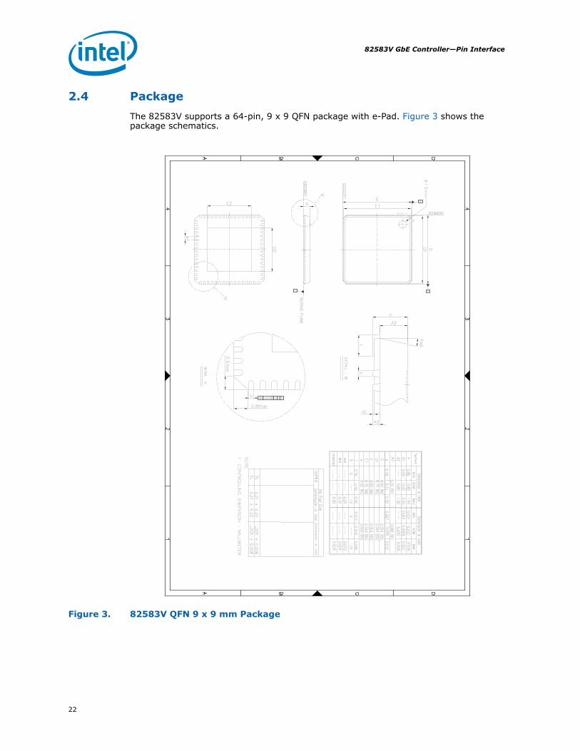
2.1 Pin AssignmentsThe 82583V supports a 64-pin, 9 x 9 QFN package with an Exposed Pad* (e-Pad*). Note that the e-Pad is ground.
Figure 2. 82583V 64-Pin, 9 x 9 QFN Package With e-Pad
CTRL19
AVD
D3p3/VD
D3p3
RSVD
2_PD
RSVD
3_PD
VD
D1p0
RSVD
5_PU
RSVD
6_PURSVD
7_PD
RSVD
8_PU
RSVD
9_PU
VD
D3p3
VD
D1p0
NVM
_SI
NVM
_SK
NVM
_SO
NVM
_CS_N
RS
ET
AVDD1p9
CTRL10
AVDD1p9
RS
VD
36_PU
NV
MT
/JTA
G_
TM
S
DIS_REG10
AU
X_P
WR
/JTA
G_T
CK
VD
D1
p0
VDD1p9
JTA
G_
TD
I
XT
AL1
AT
ES
T_N
AVD
D1p9
MDI_MINUS[0]
MDI_PLUS[0]
MDI_MINUS[1]
MDI_PLUS[1]
MDI_MINUS[2]
MDI_PLUS[2]
MDI_MINUS[3]
MDI_PLUS[3]
AVDD1p9
AVDD1p9
1 2 3 4 5 6 7 8 9 10 11 12 13 14 15 16
17
18
19
20
21
22
23
24
25
26
27
28
29
30
31
32
33343536373839404142434445464748
49
51
50
52
53
54
55
56
57
58
59
60
61
62
63
64
LED
2
AT
ES
T_P
AVD
D1p9
XT
AL2
VD
D1p0
RS
VD
34_PU
RS
VD
35_PU
PE
_WA
KE
_N/JT
AG
_TD
O
LED0
LED1
VDD3p3
PE_Tp
AVDD1p9
PE_Rn
PE_Rp
PECLKn
PECLKp
VDD1p0
DEV_OFF_N
TEST_EN
PE_RST_N
VDD1p0
PE_Tn
82583V64 Pin QFN
9 mm x 9 mm0.5 mm pin pitch
with Exposed Pad*
VDD1p0

17
Pin Interface—82583V GbE Controller
2.2 Pull-Up/Pull-Down Resistors and Strapping Options• As stated in the Name and Function table columns, the internal Pull-Up/Pull-Down
(PU/PD) resistor values are 30 KΩ ± 50%.• Only relevant (digital) pins are listed; analog or bias and power pins have specific
considerations listed in Section 3.0.• NVMT and AUX_PWR are used for a static configuration. They are sampled while
PE_RST_N is active and latched when PE_RST_N is deasserted. At other times, they revert to their standard usage.
2.3 Signal Type Definition
2.3.1 PCIe
In Input is a standard input-only signal.
Out (O) Totem pole output is a standard active driver.
T/s Tri-State is a bi-directional, tri-state input/output pin.
S/t/s
Sustained tri-state is an active low tri-state signal owned and driven by one and only one agent at a time. The agent that drives an s/t/s pin low must drive it high for at least one clock before letting it float. A new agent cannot start driving an s/t/s signal any sooner than one clock after the previous owner tri-states it.
O/d Open drain enables multiple devices to share as a wire-OR.
A-in Analog input signals.
A-out Analog output signals.
B Input bias.
Table 6. PCIe
Symbol Lead # Type Op Mode Name and Function
PECLKpPECLKn
2625 A-in Input
PCIe Differential Reference Clock InThis pin receives a 100 MHz differential clock input. This clock is used as the reference clock for the PCIe Tx/Rx circuitry and by the PCIe core PLL to generate a 125 MHz clock and 250 MHz clock for the PCIe core logic.
PE_TpPE_Tn
2120 A-out Output
PCIe Serial Data OutputSerial differential output link in the PCIe interface running at 2.5 Gb/s. This output carries both data and an embedded 2.5 GHz clock that is recovered along with data at the receiving end.

82583V GbE Controller—Pin Interface
18
2.3.2 NVM Port
2.3.3 LEDs
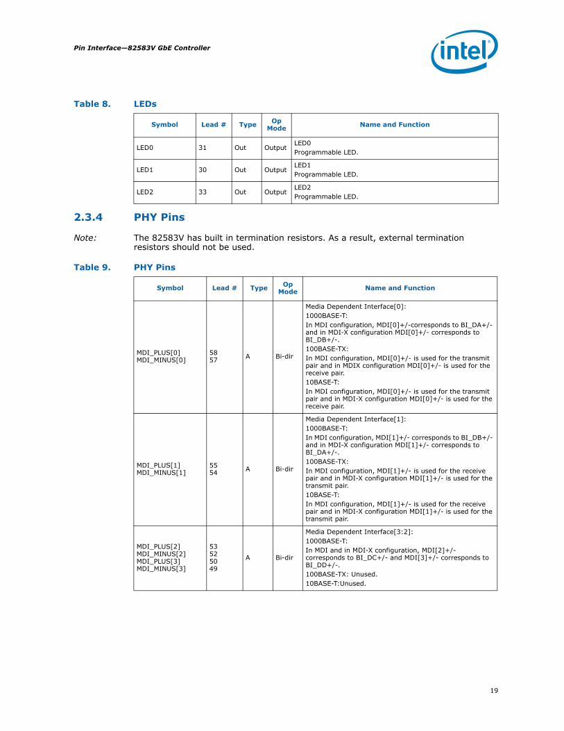
Table 8 lists the functionality of each LED output pin. The default activity of each LED can be modified in the NVM. The LED functionality is reflected and can be further modified in the configuration registers (LEDCTL).
PE_RpPE_Rn
2423 A-in Input
PCIe Serial Data InputSerial differential input link in the PCIe interface running at 2.5 Gb/s. The embedded clock present in this input is recovered along with the data.
PE_WAKE_N/JTAG_TDO 16 O/d Output
WakeThe 82583V drives this signal to zero when it detects a wake-up event and either:• The PME_en bit in PMCSR is 1b or• The APME bit of the Wake Up Control (WUC) register is
1b.JTAG TDO Output.
PE_RST_N 17 In InputPower and Clock Good Indication The PE_RST_N signal indicates that both PCIe power and clock are available.
Table 7. NVM Port
Symbol Lead # Type Op Mode Name and Function
NVM_SI 12 T/s Output
Serial Data Output Connect this lead to the input of the Non-Volatile Memory (NVM).Note: The NVM_SI port pin includes an internal pull-up resistor.
NVM_SO 14 T/s Input
Serial Data Input Connect this lead to the output of the NVM.Note: The NVM_SO port pin includes an internal pull-up resistor.
NVM_SK 13 T/s OutputNon-Volatile Memory Serial Clock Note: The NVM_SK port pin includes an internal pull-up resistor.
NVM_CS_N 15 T/s OutputNon-Volatile Memory Chip Select OutputNote: The NVM_CS port pin includes an internal pull-up resistor.
Table 6. PCIe
Symbol Lead # Type Op Mode Name and Function
19
Pin Interface—82583V GbE Controller
2.3.4 PHY Pins
Note: The 82583V has built in termination resistors. As a result, external termination resistors should not be used.
Table 8. LEDs
Symbol Lead # Type Op Mode Name and Function
LED0 31 Out OutputLED0Programmable LED.
LED1 30 Out OutputLED1Programmable LED.
LED2 33 Out OutputLED2Programmable LED.
Table 9. PHY Pins
Symbol Lead # Type Op Mode Name and Function
MDI_PLUS[0]MDI_MINUS[0]
5857 A Bi-dir
Media Dependent Interface[0]: 1000BASE-T:In MDI configuration, MDI[0]+/-corresponds to BI_DA+/- and in MDI-X configuration MDI[0]+/- corresponds to BI_DB+/-.100BASE-TX: In MDI configuration, MDI[0]+/- is used for the transmit pair and in MDIX configuration MDI[0]+/- is used for the receive pair.10BASE-T: In MDI configuration, MDI[0]+/- is used for the transmit pair and in MDI-X configuration MDI[0]+/- is used for the receive pair.
MDI_PLUS[1]MDI_MINUS[1]
5554 A Bi-dir
Media Dependent Interface[1]:1000BASE-T:In MDI configuration, MDI[1]+/- corresponds to BI_DB+/- and in MDI-X configuration MDI[1]+/- corresponds to BI_DA+/-.100BASE-TX:In MDI configuration, MDI[1]+/- is used for the receive pair and in MDI-X configuration MDI[1]+/- is used for the transmit pair.10BASE-T:In MDI configuration, MDI[1]+/- is used for the receive pair and in MDI-X configuration MDI[1]+/- is used for the transmit pair.
MDI_PLUS[2]MDI_MINUS[2]MDI_PLUS[3]MDI_MINUS[3]
53525049
A Bi-dir
Media Dependent Interface[3:2]:1000BASE-T: In MDI and in MDI-X configuration, MDI[2]+/- corresponds to BI_DC+/- and MDI[3]+/- corresponds to BI_DD+/-.100BASE-TX: Unused.10BASE-T:Unused.

82583V GbE Controller—Pin Interface
20
2.3.5 Miscellaneous and Test Pins
XTAL1XTAL2
4342
A-InA-Out
Input/Output
XTAL In/OutThese pins can be driven by an external 25 MHz crystal or driven by an external MOS level 25 MHz oscillator. Used to drive the PHY.
ATEST_PATEST_N
4546 A-out Output Positive side of the high speed differential debug port for
the PHY.
RSET 48 A BiasPHY TerminationThis pin should be connected through a 4.99 KΩ +-1% resister to ground.
Table 10. Miscellaneous and Test Pins
Symbol Lead # Type Op Mode Name and Function
DEV_OFF_N 28 In InputThis is a 3.3 V dc input signal. Asserting DEV_OFF_N puts the 82583V in device disable mode. Note that this pin is asynchronous.
TEST_EN 29 In Input
Enables Test ModeTest pins are overloaded on the functional signals as described in the pin description text of this section. The pin is active high. Note: This pin should be externally pulled down for normal operation.
AUX_PWR/JTAG_TCK 39 In Input
Auxiliary Power Indication. AUX_PWR is supported when sampled high and should be connected using a resistorJTAG Clock InputNote: The AUX_PWR/JTAG_TCK port pin includes an internal pull-down resistor.
NVMT/JTAG_TMS 38 In Input
NVM TypeThe NVM is Flash when sampled LOW and EEPROM when sampled HIGH. JTAG TMS Input.Note: The NVMT/JTAG_TMS port pin includes an internal pull-up resistor. Also note that the internal pull-up is disconnected during startup. As a result, NVMT MUST be connected externally.
JTAG_TDI 40 In InputJTAG TDI InputNote: The JTAG_TDI port pin includes an internal pull-up resistor.
Table 9. PHY Pins
Symbol Lead # Type Op Mode Name and Function

21
Pin Interface—82583V GbE Controller
2.3.6 Power Supplies and Support Pins
2.3.6.1 Power Support
2.3.6.2 Power Supply
2.3.7 Reserved Pins
Table 11. Power Support
Symbol Lead # Type / Voltage Name and Function
CTRL10 62 A-out1.05 V dc ControlVoltage control for an external 1.05 V dc PNP.
CTRL19 64 A-out1.9 V dc ControlVoltage control for an external 1.9 V dc PNP.
DIS_REG10 59 A-in
Disable 1.05 V dc RegulatorWhen high, the internal 1.05 V dc regulator is disabled and the CTRL10 signal is active. When low, the internal 1.05 V dc regulator is enabled using its internal power transistor. In this case, the CTRL10 signal is inactive.
Table 12. Power Supply
Symbol Lead # Type / Voltage Name and Function
VDD1p0 4, 11, 18, 27, 37, 41, 60
1.05 V dc 1.05 V dc power supply (7).
AVDD1p9 22, 44, 47, 51, 56, 61, 63 1.9 V dc 1.9 V dc power supply (7).
VDD3p3 10, 32 3.3 V dc 3.3 V dc power supply (2).
AVDD3p3/VDD3p3 1 3.3 V dc 3.3 V dc power supply (1).
VDD1p9 19 1.9 V dc Fuse voltage for programming on-die fuses. Connect to 1.9 V dc for normal operation.
GND e-Pad Ground The e-Pad metal connection on the bottom of the package. Should be connected to ground.
Symbol Lead # Name and Function
RSVD2_PDRSVD3_PDRSVD7_PD
237
These pins need to be pulled down using 10 KΩ resistors.
RSVD5_PURSVD6_PURSVD8_PURSVD9_PURSVD34_PURSVD35_PURSVD36_PU
5689343536
These pins need to be pulled up using 10 KΩ resistors.
82583V GbE Controller—Pin Interface
22
2.4 PackageThe 82583V supports a 64-pin, 9 x 9 QFN package with e-Pad. Figure 3 shows the package schematics.
Figure 3. 82583V QFN 9 x 9 mm Package

23
Pin Interface—82583V GbE Controller
Note: This page intentionally left blank.

82583V GbE Controller—Electrical Specifications
24
3.0 Electrical Specifications
3.1 IntroductionThis chapter describes the 82583V's electrical properties.
3.2 Voltage Regulator Power Supply Specification
3.2.1 3.3 V dc Rail
3.2.2 1.9 V dc Rail
Title Description Min Max Units
Rise Time Time from 10% to 90% mark 1 100 ms
Mononotonicity Voltage dip allowed in ramp 0 mV dc
Slope Ramp rate at any given time between 10% and 90% 2880 V dc/s
Operational Range Voltage range for normal operating conditions 3 3.6 V dc
Ripple Maximum voltage ripple @ BW = 50 MHz 70 mV
Overshoot Maximum voltage allowed 4 V dc
Capacitance Minimum capacitance 25 μF
Title Description Min Max Units
Rise Time Time from 10% to 90% mark 1 100 ms
Mononotonicity Voltage dip allowed in ramp 0 mV dc
Slope Ramp rate at any given time between 10% and 90% 1440 V dc/s
Operational Range Voltage range for normal operating conditions 1.8 2 V dc
Ripple Maximum voltage ripple @ BW = 50 MHz 50 mV dc
Overshoot Maximum voltage allowed 2.7 V dc
Output Capacitance Capacitance range when using PNP circuit 20 40 μF
Input Capacitance Capacitance range when using PNP circuit 20 μF
Capacitance ESR Equivalent series resistance of output capacitance1
1. Do not use tantalum capacitors.
5 100 mΩ
Ictrl Maximum output current rating to CTRL19 10 mA

25
Electrical Specifications—82583V GbE Controller
3.2.3 1.05 V dc Rail
3.2.4 PNP Specifications
Title Description Min Max Units
Rise Time Time from 10% to 90% mark 1 100 ms
Mononotonicity Voltage dip allowed in ramp 0 mV dc
Slope Ramp rate at any given time between 10% and 90% 800 V dc/s
Operational Range Voltage range for normal operating conditions -5 +5 %
Ripple Maximum voltage ripple @ BW = 50 MHz 50 mV dc
Overshoot Maximum voltage allowed 1.5 V dc
Output Capacitance Capacitance range when using PNP circuit 20 40 μF
Input Capacitance Capacitance range when using PNP circuit 20 μF
Capacitance ESR Equivalent series resistance of output capacitance1
1. Do not use tantalum capacitors.
10 mΩ
Ictrl Maximum output current rating to CTRL10 10 mA
Table 13. External Power Supply Specification
Title Description Min Max Units
VCBO 20 V dc
VCEO 20 V dc
IC(max) 1 A
IC(peak) 1.2 A
Ptot Minimum total dissipated power @ 25 °C ambient temperature 1.5 W
hFE DC current gain @ Vce=-10 V dc, Ic=500 mA 85
hfe AC current gain @ Ic=50mA VCE=-10 V dc, f=20 MHz 2.5
Cc collector capacitance @ VCB=-5V, f=1MHz 50 pF
fT Transition frequency @ Ic=10mA, VCE=-5 V dc, f=100 MHz 40 MHz
Recommended transistor BCP69

82583V GbE Controller—Electrical Specifications
26
3.3 Power SequencingFor proper and safe operation, the power supplies must follow the following rule:
VDD3p3 (3.3 V dc) ≥ AVDD1p9 (1.9 V dc) ≥ VDD1p0 (1.05 V dc)
This means that VDD3p3 MUST start ramping before AVDD1p8 and VDD1p0, but VDD1p0 MIGHT reach its nominal operating range before AVDD1p8 and VDD3p3.
Basically, the higher voltages must be greater than or equal to the lower voltages. This is necessary to avoid low impedance paths through clamping diodes and to eliminate back-powering.
The same requirements apply to the power-down sequence.
Internal Power On Reset must be low throughout the time that the power supplies are ramping. This guarantees that the MAC and PHY resets cleanly. While Internal Power On Reset is low, reset to the PHY is also asserted. After the power supplies are valid, Internal Power On Reset must remain low for at least tCLK125START to guarantee that the CLK125 clock from the PHY is running.
3.4 Power-On Reset• Power up sequence – 3.3 V dc -> 1.9 V dc -> 1.05 V dc• Power down sequence 1.05 V dc -> 1.9 V dc->3.3 V dc
Table 14. Power Detection Thresholds
Symbol Parameter Specifications Units
Min Typ Max
V1a High threshold for 3.3 V dc supply 1.35 1.7 2.0 V dc
V2a Low threshold for 3.3 V dc supply 1.35 1.6 1.9 V dc
V1b High threshold for 1.05 V dc supply 0.6 0.7 0.75 V dc
V2b Low threshold for 1.05 V dc supply 0.35 0.45 0.6 V dc

27
Electrical Specifications—82583V GbE Controller
3.5 Power Scheme SolutionsFigure 4 shows the intended design options for power solutions. The values for the various components in Figure 4 are listed in Table 15; Table 16 and Table 17 list the power consumption values.
Figure 4. Power Scheme Schematics
3.3 V dc
C1
CTRL10
OPTION B:External 1.05 V dc
1.9 V dc PnP Transistor Regulator
OPTION A:Fully Integrated 1.05 V dc Regulator
1.9 V dc PnP Transistor Regulator
X
C3
C4
R1
R
3.3 V dc
3.3 V dc
C1
CTRL10VDD3p3 VDD3p3
AVDD1p9 AVDD1p9
VDD1p0
3.3 V dc
1 K ohm
DIS_REG10
1 K ohm
DIS_REG10
82583V 82583V
C2
VDD1p0
X
3.3 V dc
C1
CTRL10VDD3p3
AVDD1p9
DIS_REG10
82583V
C2
1.05 V dc
VDD1p0
X
1.9 V dc
C4
OPTION C:All External Power Supplies
C3
C4
R1
R
3.3 V dc
R
3.3 V dc
C4
R2
C5
3.3 V dc
1 K ohm CTRL19
CTRL19CTRL19
OPTION D:Fully Integrated 1.05 V dc
External 1.9 V dc Regulator
X
3.3 V dc
C1
CTRL10VDD3p3
AVDD1p9
82583V
CTRL19
C4
External 1.9 V dcRegulator
3.3 V dcX
VDD1p0
C2
DIS_REG10
1 K ohm

82583V GbE Controller—Electrical Specifications
28
Table 15. Parameters For Power Scheme Options
Notes:1. All capacitors are ceramic type.2. 10 μF capacitance can be 2 x 4.7 μF.3. 22 μF can be 2 x 10 μF or 4 x 4.7 μF for 1.9 V dc bypass. 4. Place 0.1 μF capacitors near pins.5. PNP must be placed 0.5-inch (10 mm) from the 82583V.6. VDD1p0 pins are connected together by a plane.
Note: The following numbers apply to device current and power and do not include power losses on external components.
Table 16. Options B and C Power Consumption (External 1.05 V dc Regulator)
Option A Option B1 Option C Option D
C1 10 μF 10 μF 10 μF 10 μF
C2 22 μF + 0.1 μF (multiple) 10 μF 22 μF + 0.1 μF
(multiple)22 μF + 0.1 μF (multiple)
C3 10μF 10 μF
C4 10 μF +0.1 μF (multiple near pins)
22 μF + 0.1 μF (multiple near pins)
10 μF +0.1 μF (multiple near pins)
C5 10 μF +0.1 μF (multiple near pins)
R1 0 Ω 0 Ω
R2 0 Ω
R 5 KΩ 5 KΩ
1. 1.05 V dc PNP uses 1.9 V dc from PNP.
State Mode 3.3 [mA]
1.9 [mA]
1.05 [mA]
Power [mW]
S0 - Maximum 1000Base-T active, 90 °C 5 266 195 727
S0 - Typical
1000Base-T active 4 261 184 702
1000Base-T idle 4 217 108 539
100Base-T active 4 116 60 296
100Base-T idle 4 71 22 171
10Base-T active 4 162 48 372
10Base-T idle 4 70 11 157
Cable disconnect 4 14 5 45
LAN disable 4 13 2 40
SX
D3 cold with WOL 100 Mb/s 4 71 22 171
D3 cold with WOL 10 Mb/s 4 70 11 157
D3 cold without WOL 4 8 5 34

29
Electrical Specifications—82583V GbE Controller
Table 17. Options A and D Power Consumption (Fully Integrated 1.05 V dc Regulator)
State Mode 3.3 [mA]
1.9 [mA]
Power [mW]
S0 - Maximum 1000Base-T active, 90 °C 5 471 911
S0 - Typical
1000Base-T active 4 455 878
1000Base-T idle 4 331 642
100Base-T active 4 178 351
100Base-T idle 4 93 190
10Base-T active 4 212 416
10Base-T idle 4 81 167
Cable disconnect 4 18 44
LAN disable 4 12 36
SX
D3 cold with WOL 100 Mb/s 4 92 188
D3 cold with WOL 10 Mb/s 4 81 167
D3 cold without WOL 4 13 35

82583V GbE Controller—Electrical Specifications
30
3.6 Flash AC SpecificationsThe 82583V is designed to support a serial flash. Applicable over the recommended operating range from Ta = -40 °C to +85 °C, VCC3P3 = 3.3 Vdc, Cload = 1 TTL Gate and 16 pF (unless otherwise noted).
Figure 5. Flash Timing Diagram
Symbol Parameter Min Typ Max Units Note
tSCK SCK clock frequency 0 15.625 20 MHz [1]
tRI Input rise time 2.5 20 ns
tFI Input fall time 2.5 20 ns
tWH SCK high time 20 32 ns [2]
tWL SCK low time 20 32 ns [2]
tCS CS high time 25 ns
tCSS CS setup time 25 ns
tCSH CS hold time 25 ns
tSU Data-in setup time 5 ns
tH Data-in hold time 5 ns
tV Output valid 20 ns
tHO Output hold time 0 ns
tDIS Output disable time 100 ns
Notes:1. Clock is 62.5 MHz divided by 4. In bit banging mode maximum allowable frequency is 20 MHz.2. 45% to 55% duty cycle.
CS
VIH
VIL
VIH
VIL
VIH
VIL
Sck
VALID INSI
VOH
VOL
HI-ZSO
HO DIStt
WHWL
CSH
CSt
t t
tt
CSS
SU Ht t
HI-Z
valt

31
Electrical Specifications—82583V GbE Controller
3.7 EEPROM AC SpecificationsThe 82583V is designed to support a standard serial EEPROM. Applicable over recommended operating range from Ta = -40 °C to +85 °C, VCC3P3 = 3.3 Vdc, Cload = 1 TTL Gate and 16 pF (unless otherwise noted).
Figure 6. EEPROM Timing Diagram
Symbol Parameter Min Typ Max Units Note
tSCK SCK clock frequency 0 2 2.1 MHz [1]
tRI Input rise time 2 µs
tFI Input fall time 2 µs
tWH SCK high time 200 250 ns [2]
tWL SCK low time 200 250 ns
tCS CS high time 250 ns
tCSS CS setup time 250 ns
tCSH CS hold time 250 ns
tSU Data-in setup time 50 ns
tH Data-in hold time 50 ns
tV Output valid 0 200 ns
tHO Output hold time 0 ns
tDIS Output disable time 250 ns
Notes:1. Clock is 2 MHz.2. 45% to 55% duty cycle.
VALID IN
CS
VIH
VIH
VIL
VIH
VIL
Sck
SI
VOH
VOL
HI-ZSO
WHWL
CSH
CSt
t t
tt
CSS
SUtHt
HO DIStt
HI-Z
valt

82583V GbE Controller—Electrical Specifications
32
3.8 Discrete/Integrated Magnetics Specifications
Criteria Condition Values (Min/Max)
Voltage Isolation
At 50 to 60 Hertz for 60 seconds 1500 Vrms (min)
For 60 seconds 2250 V dc (min)
Open Circuit Inductance (OCL) or OCL (alternate)
With 8 mA DC bias at 25 °C 400 μH (min)
With 8 mA DC bias at 0 °C to 70 °C 350 μH (min)
Insertion Loss
100 kHz through 999 kHz1.0 MHz through 60 MHz60.1 MHz through 80 MHz80.1 MHz through 100 MHz100.1 MHz through 125 MHz
1 dB (max)0.6 dB (max)0.8 dB (max)1.0 dB (max)2.4 dB (max)
Return Loss
1.0 MHz through 40 MHz40.1 MHz through 100 MHz
When reference impedance si 85 Ω, 100 Ω, and 115 Ω.
Note that return loss values might vary with MDI trace lengths. The LAN magnetics might need to be measured in the platform where it is used.
18 dB (min)12 to 20 * LOG (frequency in MHz / 80) dB (min)
Crosstalk Isolation Discrete Modules
1.0 MHz through 29.9 MHz30 MHz through 250 MHz250.1 MHz through 375 MHz
-50.3+(8.8*(freq in MHz / 30)) dB (max)-26-(16.8*(LOG(freq in MHz / 250)))) dB (max)-26 dB (max)
Crosstalk Isolation Integrated Modules
1.0 MHz through 10 MHz10.1 MHz through 100 MHz100.1 MHz through 375 MHz
-50.8+(8.8*(freq in MHz / 10)) dB (max)-26-(16.8*(LOG(freq in MHz / 100)))) dB (max)-26 dB (max)
Diff to CMR1.0 MHz through 29.9 MHz30 MHz through 500 MHz
-40.2+(5.3*((freq in MHz / 30)) dB (max)-22-(14*(LOG((freq in MHz / 250)))) dB (max)
CM to CMR1.0 MHz through 270 MHz270.1 MHz through 300 MHz300.1 MHz through 500 MHz
-57+(38*((freq in MHz / 270)) dB (max)-17-2*((300-(freq in MHz) / 30) dB (max)-17 dB (max)
33
Electrical Specifications—82583V GbE Controller
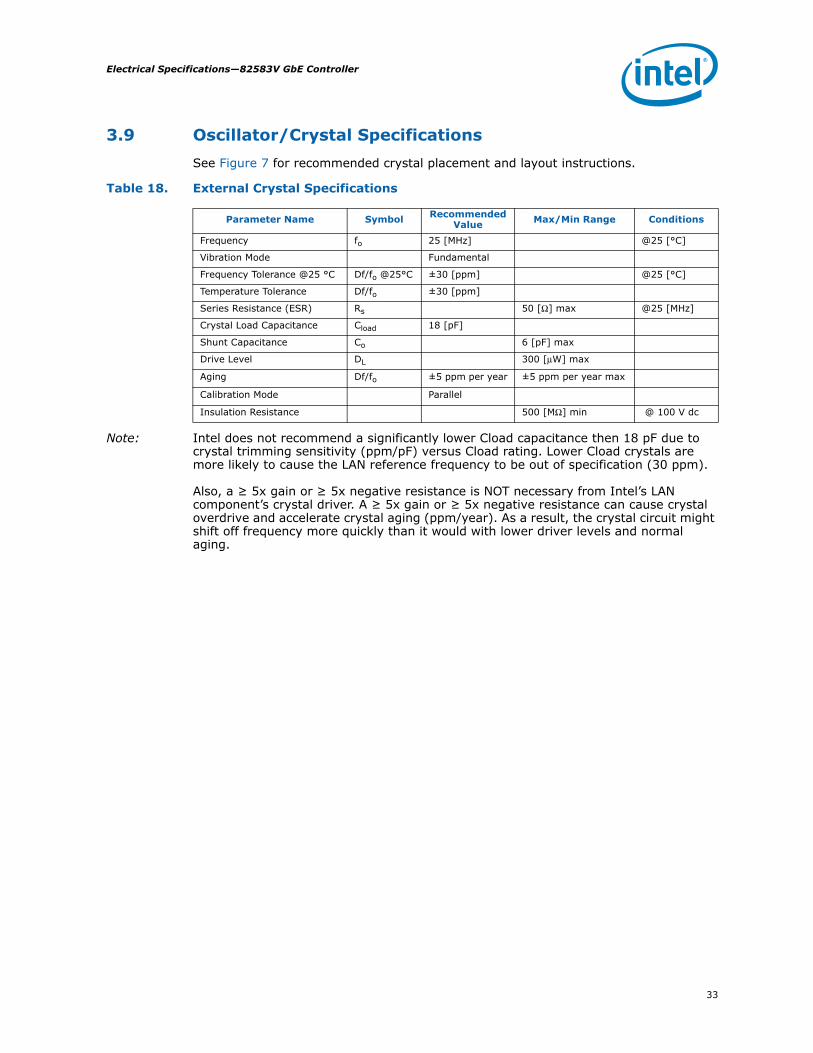
3.9 Oscillator/Crystal SpecificationsSee Figure 7 for recommended crystal placement and layout instructions.
Table 18. External Crystal Specifications
Note: Intel does not recommend a significantly lower Cload capacitance then 18 pF due to crystal trimming sensitivity (ppm/pF) versus Cload rating. Lower Cload crystals are more likely to cause the LAN reference frequency to be out of specification (30 ppm).
Also, a ≥ 5x gain or ≥ 5x negative resistance is NOT necessary from Intel’s LAN component’s crystal driver. A ≥ 5x gain or ≥ 5x negative resistance can cause crystal overdrive and accelerate crystal aging (ppm/year). As a result, the crystal circuit might shift off frequency more quickly than it would with lower driver levels and normal aging.
Parameter Name Symbol Recommended Value Max/Min Range Conditions
Frequency fo 25 [MHz] @25 [°C]
Vibration Mode Fundamental
Frequency Tolerance @25 °C Df/fo @25°C ±30 [ppm] @25 [°C]
Temperature Tolerance Df/fo ±30 [ppm]
Series Resistance (ESR) Rs 50 [Ω] max @25 [MHz]
Crystal Load Capacitance Cload 18 [pF]
Shunt Capacitance Co 6 [pF] max
Drive Level DL 300 [μW] max
Aging Df/fo ±5 ppm per year ±5 ppm per year max
Calibration Mode Parallel
Insulation Resistance 500 [MΩ] min @ 100 V dc

82583V GbE Controller—Electrical Specifications
34
Table 19. Clock Oscillator Specifications
Note: Peak-to-peak voltage presented at the XTAL1 input cannot exceed 1.9 V dc.
Figure 7. XTAL Timing Diagram
3.10 I/O DC ParametersThis section specifies the timing and electrical parameters for the various I/O interfaces.
Parameter Name Symbol/Parameter Conditions Min Typ Max Unit
Frequency fo @25 [°C] 25.0 MHz
Swing Vp-p1 3 3.3 3.6 V
Frequency Tolerance f/fo -20 to +70 ±50 [ppm]
Operating Temperature Topr -20 to +70 [°C]
Aging f/fo ±5 ppm per year [ppm]
Coupling capacitor Coupling 12 15 18 [pF]
TH_XTAL_IN XTAL_IN High Time 13 20 nS
TL_XTAL_IN XTAL_IN Low Time 13 20 nS
TJ_XTAL_IN XTAL_IN Total Jitter 2001
1. Broadband peak-to-peak = 200 pS, Broadband rms = 3 pS, 12 KHz to 20 MHz rms = 1 ps.
pS

35
Electrical Specifications—82583V GbE Controller
3.10.1 LEDs
Symbol/Parameter Conditions Min Typ Max Unit
VDD3p3 3.0 3.3 3.6 V dc
Input leakage 0<Vin<VDD3p3 10 μA
Iol @ VOL=0.4 V dc 12 mA
Ioh @ VOH=VDDO-0.4 V dc 12 mA
Cin 5 pF

82583V GbE Controller—Initialization
36
4.0 Initialization
4.1 IntroductionThis chapter discusses initialization steps. This includes:
• General hardware power-up state• Basic device configuration• Initialization of transmit and receive operation• Link configuration and software reset capability• Statistics initialization
4.2 Reset OperationThe 82583V reset sources are as follows:
• Internal Power On Reset- The 82583V has an internal mechanism for sensing the power pins. Once power is up and stable, the 82583V implements an internal reset. This reset acts as a master reset of the entire chip. It is level sensitive, and while it is 0b holds all of the registers in reset. Internal Power On Reset is an indication that device power supplies are all stable. Internal Power On Reset changes state during system power up.
• PE_RST_N - Indicates that both the power and the PCIe clock sources are stable; a value of 0b indicates reset active. This pin asserts an internal reset also after a D3cold exit. Most units are reset on the rising edge of PE_RST_N. The only exception is the PCIe unit, which is kept in reset while PE_RST_N is active.
• Device Disable/Dr Disable - The 82583V enters a device disable mode when the DEV_OFF_N pin is asserted without shutdown (see Section 8.4.4.4). The 82583V enters Dr disable mode when certain conditions are met in the Dr state (see Section 8.4.4.3).
• In-band PCIe reset - The 82583V generates an internal reset in response to a Physical Layer (PHY) message from PCIe or when the PCIe link goes down (entry to polling or detect state). This reset is equivalent to PCI reset in previous (PCI) GbE controllers.
• D3hotD0 transition - This is also known as ACPI reset. The 82583V generates an internal reset on the transition from D3hot power state to D0 (caused after configuration writes from D3 to D0 power state). Note that this reset is per function and resets only the function that transitioned from D3hot to D0.
• Software Reset - Software can reset the 82583V by writing the Device Reset bit of the Device Control (CTRL.RST) register. The 82583V re-reads the per-function NVM fields after a software reset. Bits that are normally read from the NVM are reset to their default hardware values. Note that this reset is per function and resets only the function that received the software reset. PCI configuration space (configuration and mapping) of the device is unaffected.

37
Initialization—82583V GbE Controller
• EEPROM Reset - Writing a 1b to the EEPROM Reset bit of the Extended Device Control (CTRL_EXT.EE_RST) register causes the 82583V to re-read the per-function configuration from the NVM, setting the appropriate bits in the registers loaded by the NVM.
• PHY Reset - Software can write a 1b to the PHY Reset bit of the Device Control (CTRL.PHY_RST) register to reset the internal PHY.
The resets affect the following registers and logic:
Table 20. 82583V Resets
Notes:1. If D3cold is not supported, the wake-up context is reset (PME_Status and PME_En
bits).2. Refers to bits in the Wake-Up Control (WUC) register that are not part of the wake-
up context (the PME_En and PME_Status bits).3. The Wake-Up Status (WUS) registers include the following:
— WUS register.— Wake-up packet length.— Wake-up packet memory.
Reset Name
Reset activation
Internal Power On Reset
PE_RST_N
Device/Dr Disable
In-band PCIe Reset
D3hot D0
SW Reset
EE Reset
PHY Reset Notes
PCIe Data Path √ √ √ √
Load NVM √ √ √ √ 6 √ √
PCI Config Registers RO √ √ √ √
PCI Config Registers RW √ √ √ √ √
Data path √ √ √ √ √ √ 4
Wake Up (PM) Context √ 1 √
Wake Up Control Register
√ √ 2
Wake Up Status Registers
√ √ 3
PHY √ √ √ √ √ √
Strapping Pins √ √ √ √
82583V GbE Controller—Initialization
38
4. The following register fields do not follow the previously mentioned general rules:— Packet Buffer Allocation (PBA) - reset on Internal Power On Reset only.— Packet Buffer Size (PBS) - reset on Internal Power On Reset only.— LED configuration registers.— The Aux Power Detected bit in the PCIe Device Status register is reset on
Internal Power On Reset and PCIe Power Good only.— FLA - reset on Internal Power On Reset only.
5. The NVM is loaded only when the LAN function exits D3hot state.
In situations where the device is reset using the software reset CTRL.RST, the TX data lines will be forced to all zeros. This causes a substantial number of symbol errors to be detected by the link partner.
4.3 Power Up
4.3.1 Power-Up Sequence
Figure 8 through Figure 14 shows the 82583V’s power-up sequencing.
Figure 8 shows a high-level view of the power sequence, while Figure 9 through Figure 14 provides a more detailed description of each state.

39
Initialization—82583V GbE Controller
Figure 8. 82583V Power Up - General Flow
A B
Flash EEPROM
Start
Power-On-Reset
Load EEPROMLoad Flash
C
Initialize PHY
D
Read NVM after PERST# de-assertion
E
Initialize PCIe and PHY
Bring up PCIe link

82583V GbE Controller—Initialization
40
Figure 9. 82583V Initialization - Power-On Reset
Stage
Comments
Duration (ms) Note
LegendPower ramp up
(3.3 V dc, 1.9 V dc, 1.05 V dc)
Start
Xosc stabe
From power-up
<10
Internal power-on-reset triggers
From power-up
<50
82583V samples NVMT strapping
Determine NVM type
0
A B
Flash EEPROM
Start

41
Initialization—82583V GbE Controller
Figure 10. 82583V Initialization - Flash Load
Notes:1. A 4 KB sector is read in a single burst, so the packet overhead is negligible. The
rate is 4 KB x 8 bits / 15.625 Mb/s = 2.1 ms.2. The shadow RAM is read at the rate of one word every ~3 clocks of 62.5 MHz, or
~50 ns per word. The 64 words are read in 3.2 ms.3. Clear write protection is required for an SST* Flash only. The instruction codes that
are required to initiate are hardwired in the design as defined by SST 25xxx Flash family: code 0x50 for write status enable and code 0x01 for status write. The 82583V writes a data of 0x00 to the status word which clears all protection. Software accesses to the Flash are not executed until this step completes.
Read signature at word 0x12
~0
Load sector 0 to Shadow RAM
Set EEC.SHADV & clear EEC.SEL1VAL~2.1 1
Read signature at word 2K+0x12
~0
Load base area (0x00-0x40) from Shadow
RAM
~0.0032 2
A
Good signature
Bad signature
C
Good signature
Bad signature
Load sector 1 to Shadow RAM
Set EEC.SHADV & set EEC.SEL1VAL~2.1 1
82583V set to default values
Set EEC.Auto_RD
0
Clear Write Protection
Set Flash write status enable and write status
0.008 3
82583V GbE Controller—Initialization
42
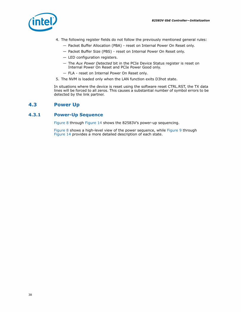
Figure 11. 82583V Initialization - EEPROM Load
Each word is read separately using a 5-byte command (1 byte instruction, 2 byte address, and 2 byte data). Total time at 2 Mb/s is 64 words x 5 bytes x 8 bits/2 Mb/s = 1.28 ms. The rate is 20 μs per word.
Detect Address length of 1B or 2B based on
signature
~0
Load base area (0x00-0x40) from EEPROM
Set EEC.Auto_RD
~1.28 3
B
Good signature
Bad signature
C
82583V set to default values
Set EEC.Auto_RD
0

43
Initialization—82583V GbE Controller
Figure 12. 82583V PHY Initialization
Each PCIe register write takes ~20 PCIe clocks (31.25 MHz) per table entry <=> 640 ns per Dword. Each PHY register write takes those 20 clocks + 64 MDC cycles on the MDIO interface (2.5 MHz) => 26.24 ms per Dword. Therefore, the total is 640 ns x 4 + 26.24 ms x 16 = 422 ms.
Each PCIe register write takes ~20 PCIe clocks (31.25 MHz) per table entry <=> 640 ns per Dword. Therefore, the bottleneck is the EEPROM at 40 ms per Dword. Each PHY register write takes those 20 clocks + 64 MDC cycles on the MDIO interface (2.5 MHz) => 26.24 ms per Dword. Therefore, the bottleneck is the EEPROM at 40 ms per Dword. The 16+4 entries take 20 Dwords x 40 ms = 0.8 s.
Enable wake up based on NVM configuration
~0
C
D
Enable the PHY if needed
PHY was inactive up to now
11

82583V GbE Controller—Initialization
44
Figure 13. 82583V Initialization - NVM Load After PE_RST_N
PERST# is de-asserted by the platform
PHY is powered down
~0
D
NVMT strapping is sampled
Determine NVM type
~0
Flash EEPROMNo NVM
Load base area (0x00-0x40) from Shadow
RAMSet EEC.Auto_RD
~0.0032 2
Load base area (0x00-0x40) from EEPROM
Set EEC.Auto_RD
~1.28 3
82583V set to default values
Set EEC.Auto_RD
0
E
Check valid Shadow and signature
~0
Detect Address length of 1B or 2B based on
signature
~0

45
Initialization—82583V GbE Controller
Figure 14. 82583V Initialization - PHY and PCIe
E
Enable the PHY
PHY was in power-down during NVM load
11
Start PCIe link training
Must start < 20 µs after PERST# de-assertion
PCIe link ready to accept configuration
requestsMust start < 100 µs
after PERST#
82583V GbE Controller—Initialization
46
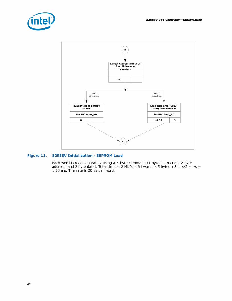
4.3.2 Timing Diagram
Figure 15. Power-Up Timing Diagram
Table 21. Notes to Power-Up Timing Diagram
D-State D0u
NVM Load
D0a
PHY State
PCIe Link up L0
Wake
4
5
7
Dr
8
9
10
3
Power
Power-On-Reset (internal)
2
PCIe reference clock
PERST#
Xosc
1
6
txog
tee tee
11 12
tpgtrn
13tpgrestpgcfg
tPWRGD-CLK
tPVPGL
tppg
AutoRead
Ext.Conf.
AutoRead
Ext.Conf.
Powered-down Active / Down
Note
1 Xosc is stable txog after power is stable
2 Internal reset is released after all power supplies are good and tppg after Xosc is stable.
3 An NVM read starts on the rising edge of the internal reset or Internal Power On Reset#.
4 After reading the NVM, PHY might exit power down mode.
5 APM wake up might be enabled based on NVM contents.
6 The PCIe reference clock is valid tPWRGD-CLK before the de-assertion of PE_RST_N (according to PCIe specification).
7 PE_RST_N is de-asserted tPVPGL after power is stable (according to PCIe specification).
8 De-assertion of PE_RST_N causes the NVM to be re-read, asserts PHY power-down, and disables Wake Up.
9 After reading the NVM, PHY exits power-down mode.
10 Link training starts after tpgtrn from PE_RST_N de-assertion.
11 A first PCIe configuration access might arrive after tpgcfg from PE_RST_N de-assertion.
12 A first PCI configuration response can be sent after tpgres from PE_RST_N de-assertion
13 Writing a 1b to the Memory Access Enable bit in the PCI Command register transitions the device from D0u to D0 state.

47
Initialization—82583V GbE Controller
4.4 Global Reset (PE_RST_N, PCIe In-Band Reset)
4.4.1 Reset Sequence
Figure 16 and Figure 17 show the 82583V's sequence following global reset (PE_RST_N de-assertion or PCIe in-band reset) and until the device is ready to accept host commands.
Figure 16. 82583V Global Reset - NVM Load
Reset (PE_RST_# de-assertion or in-band)
PHY is powered down
~0
NVMT strapping is sampled
Determine NVM type
~0
Flash EEPROMNo NVM
Load base area (0x00-0x40) from Shadow
RAMSet EEC.Auto_RD
~0.0032 2
Load base area (0x00-0x40) from EEPROM
Set EEC.Auto_RD
~1.28 3
82583V set to default values
Set EEC.Auto_RD
0
A
Check valid Shadow and signature
~0
Detect Address length of 1B or 2B based on
signature
~0

82583V GbE Controller—Initialization
48
Figure 17. 82583V Global Reset - PHY and PCIe
4.4.2 Timing Diagram
The following timing diagram shows the 82583V’s behavior through a PE_RST_N reset.
A
Enable the PHY
PHY was in power-down during NVM load
11
Start PCIe link training
Must start < 80 µs after PERST# de-assertion
PCIe link ready to accept configuration
requestsMust start < 100 µs
after PERST#

49
Initialization—82583V GbE Controller
Figure 18. Global Reset Timing Diagram
Table 22. Notes to Global Reset Timing Diagram
D-State D0u
NVM Load
D0a
PHY State
PCIe Link up L0
Wake
2
1
Dr
4
5
7
PCIe reference clock
PERST#
tee
8 9
tpgtrn
10tpgrestpgcfg
AutoRead
Ext.Conf.
Active Active / Down
tclkpg
L0
Any mode APM
D0a
3tPWRGD-CLK
6
Note
1The system must assert PE_RST_N before stopping the PCIe reference clock. It must also wait tl2clk after link transition to L2/L3 before stopping the reference clock.
2 On assertion of PE_RST_N, the 82583V transitions to Dr state and the PCIe link transition to electrical idle. The PHY state is defined by the wake configuration.
3 The system starts the PCIe reference clock tPWRGD-CLK before de-assertion PE_RST_N.
4 De-assertion of PE_RST_N causes the NVM to be re-read, asserts PHY power-down, and disables wake up.
5 After reading the NVM base area, PHY reset is de-asserted. APM wake might be enabled.
6 Link training starts after the NVM was fully read (including extended configuration if needed).
7 Link training starts after tpgtrn from PE_RST_N de-assertion.
8 A first PCIe configuration access might arrive after tpgcfg from PE_RST_N de-assertion.
9 A first PCI configuration response can be sent after tpgres from PE_RST_N de-assertion.
10 Writing a 1b to the Memory Access Enable bit in the PCI Command register transitions the device from D0u to D0 state.

82583V GbE Controller—Initialization
50
4.5 Timing Parameters
4.5.1 Timing Requirements
The 82583V requires the following start-up and power state transitions.
Table 23. Timing Requirements
4.5.2 MDIO and NVM Semaphore
The MDIO and NVM semaphore mechanism resolved possible conflicts between software and hardware access to the MDIO and NVM (the latter applies only to software accesses through the EERD register). The mechanism does not block software accesses to MDIO or the NVM, therefore programmers can enable software to use or ignore this process at will. For example, software might track the hardware state through other means (such as, a software state machine) and avoid any MDIO and NVM accesses when hardware is in configuration states. However, hardware must comply with the protocol.The EXTCNF_CTRL.MDIO/NVM SW Ownership bit, EXTCNF_CTRL.MDIO MNG Ownership bit and the EXTCNF_CTRL.MDIO/NVM HW Ownership bit provide a mechanism for software, manageability and hardware entities to arbitrate for accesses to MDIO and NVM. Software arbitration for NVM accesses is only required when done through the EERD register. A request for ownership is registered by writing a 1b into the respective bit (software writes to the MDIO/NVM SW Ownership bit, manageability writes to the MDIO MNG Ownership bit and hardware writes to the MDIO/NVM HW Ownership). The requesting agent is granted access when the same bit is read as 1b (access is not granted as long as the bit is 0b). The MDIO/NVM SW Ownership and the MDIO/NVM HW Ownership bits are cleared on reset, while the MDIO MNG Ownership bit is reset only by LAN_PWR_GOOD (or if the firmware clears it). The 82583 guarantees that at any given time at most only one bit is 1b. Access is granted when a bit is actually written with 1b and the other bits are 0b. Once the access completes, the controlling agent must write a 0b to its ownership bit to enable accesses by the other agents.
The 82583’s hardware sets the bit while loading the extended configuration area.
Parameter Description Min Max Notes
txog Xosc stable from power stable 10 ms
tPWRGD-CLK PCIe clock valid to PCIe power good 100 μs - According to PCIe specification.
tPVPGL Power rails stable to PCIe PE_RST_N inactive 100 ms - According to PCIe specification.
Tpgcfg External PE_RST_N signal to first configuration cycle. 100 ms According to PCIe specification.
td0mem Device programmed from D3h to D0 state to next device access 10 ms According to PCI power
management specification.
tl2pg L2 link transition to PE_RST_N assertion 0 ns According to PCIe specification.
tl2clk L2 link transition to removal of PCIe reference clock 100 ns According to PCIe specification.
Tclkpg PE_RST_N assertion to removal of PCIe reference clock 0 ns According to PCIe specification.
Tpgdl PE_RST_N assertion time 100 μs According to PCIe specification.

51
Initialization—82583V GbE Controller
4.6 Software Initialization SequenceThe following sequence of commands is typically issued to the device by the software device driver in order to initialize the 82583V to normal operation. The major initialization steps are:1. Disable Interrupts - see Interrupts during initialization.2. Issue Global Reset and perform General Configuration - see Global Reset and
General Configuration.3. Setup the PHY and the link - see Link Setup Mechanisms and Control/Status Bit
Summary.4. Initialize all statistical counters - see Initialization of Statistics.5. Initialize Receive - see Receive Initialization.6. Initialize Transmit - see Transmit Initialization.7. Enable Interrupts - see Interrupts during initialization.
4.6.1 Interrupts During Initialization
Most drivers disable interrupts during initialization to prevent re-entrancy. Interrupts are disabled by writing to the IMC register. Note that the interrupts need to be disabled also after issuing a global reset, so a typical driver initialization flow is:1. Disable interrupts2. Issue a global reset3. Disable interrupts (again)4. …
After the initialization completes, a typical driver enables the desired interrupts by writing to the IMS register.
4.6.2 Global Reset and General Configuration
Device initialization typically starts with a global reset that puts the device into a known state and enables the software device driver to continue the initialization sequence.
Several values in the Device Control (CTRL) register need to be set at power up or after a device reset for normal operation.
• Full duplex should be set per interface negotiation (if done in software), or is set by the hardware if the interface is auto-negotiating. This is reflected in the Device Status register in the auto-negotiating case. A default value is loaded from the NVM.
• Speed is determined via auto-negotiation by the PHY, or forced by software if the link is forced. Status information for speed is also readable in STATUS.
• ILOS should normally be set to 0b.
If using XOFF flow control, program the FCAH, FCAL, and FCT registers. If not, they should be written with 0x0.
GCR bit 22 should be set to 1b by software during initialization.

82583V GbE Controller—Initialization
52
4.6.3 Link Setup Mechanisms and Control/Status Bit Summary
4.6.3.1 PHY Initialization
Refer to the PHY documentation for the initialization and link setup steps. The device driver uses the MDIC register to initialize the PHY and setup the link.
4.6.3.2 MAC/PHY Link Setup
This section summarizes the various means of establishing proper MAC/PHY link setups, differences in MAC CTRL register settings for each mechanism, and the relevant MAC status bits. The methods are ordered in terms of preference (the first mechanism being the most preferred).• MAC settings automatically based on duplex and speed resolved by PHY.
(CTRL.FRCDPLX = 0b, CTRL.FRCSPD = 0b, CTRL.ASDE = 0b)— CTRL.FD - Don't care; duplex setting is established from PHY's internal
indication to the MAC (FDX) after PHY has auto-negotiated a successful link-up.— CTRL.SLU - Must be set to 1b by software to enable communications between
MAC and PHY.— CTRL.RFCE - Must be set by software after reading flow control resolution from
PHY registers.— CTRL.TFCE - Must be set by software after reading flow control resolution from
PHY registers.— CTRL.SPEED - Don't care; speed setting is established from PHY's internal
indication to the MAC (SPD_IND) after PHY has auto-negotiated a successful link-up.
— STATUS.FD - Reflects the actual duplex setting (FDX) negotiated by the PHY and indicated to the MAC.
— STATUS.LU - Reflects link indication (LINK) from the PHY qualified with CTRL.SLU (set to 1b).
— STATUS.SPEED - Reflects actual speed setting negotiated by the PHY and indicated to the MAC (SPD_IND).
• MAC duplex setting automatically based on resolution of PHY, software-forced MAC/PHY speed. (CTRL.FRCDPLX = 0b, CTRL.FRCSPD = 1b, CTRL.ASDE = don't care)— CTRL.FD - Don't care; duplex setting is established from PHY's internal
indication to the MAC (FDX) after PHY has auto-negotiated a successful link-up.— CTRL.SLU - Must be set to 1b by software to enable communications between
the MAC and PHY.— CTRL.RFCE - Must be set by software after reading flow control resolution from
PHY registers.— CTRL.TFCE - Must be set by software after reading flow control resolution from
the PHY registers.— CTRL.SPEED - Set by software to desired link speed (must match speed setting
of PHY).— STATUS.FD - Reflects the actual duplex setting (FDX) negotiated by the PHY
and indicated to MAC.— STATUS.LU - Reflects link indication (LINK) from the PHY qualified with
CTRL.SLU (set to 1b).— STATUS.SPEED - Reflects MAC forced speed setting written in CTRL.SPEED.

53
Initialization—82583V GbE Controller
• MAC duplex and speed settings forced by software based on resolution of PHY. (CTRL.FRCDPLX = 1b, CTRL.FRCSPD = 1b, CTRL.ASDE = don't care)— CTRL.FD - Set by software based on reading PHY status register after the PHY
has auto-negotiated a successful link-up.— CTRL.SLU. - Must be set to 1b by software to enable communications between
the MAC and PHY.— CTRL.RFCE - Must be set by software after reading flow control resolution from
the PHY registers.— CTRL.TFCE - Must be set by software after reading flow control resolution from
the PHY registers.— CTRL.SPEED - Set by software based on reading PHY status register after the
PHY has auto-negotiated a successful link-up.— STATUS.FD - Reflects the MAC forced duplex setting written to CTRL.FD.— STATUS.LU - Reflects link indication (LINK) from the PHY qualified with
CTRL.SLU (set to 1b).— STATUS.SPEED - Reflects MAC forced speed setting written in CTRL.SPEED.
• MAC/PHY duplex and speed settings both forced by software (fully-forced link setup). (CTRL.FRCDPLX = 1b, CTRL.FRCSPD = 1b, CTRL.SLU = 1b)— CTRL.FD - Set by software to desired full-/half- duplex operation (must match
duplex setting of the PHY).— CTRL.SLU - Must be set to 1b by software to enable communications between
the MAC and PHY. The PHY must also be forced/configured to indicate positive link indication (LINK) to the MAC.
— CTRL.RFCE - Must be set by software to the desired flow-control operation (must match flow-control settings of the PHY).
— CTRL.TFCE - Must be set by software to the desired flow-control operation (must match flow-control settings of the PHY).
— CTRL.SPEED - Set by software to desired link speed (must match speed setting of the PHY).
— STATUS.FD - Reflects the MAC duplex setting written by software to CTRL.FD.— STATUS.LU - Reflects 1b (positive link indication LINK from PHY qualified with
CTRL.SLU).
Note: Since both CTRL.SLU and the PHY link indication LINK are forced, this bit set does not guarantee that operation of the link has been truly established.
— STATUS.SPEED - Reflects MAC forced speed setting written in CTRL.SPEED.
4.6.4 Initialization of Statistics
Statistics registers are hardware-initialized to values as detailed in each particular register's description. The initialization of these registers begins at transition to D0 active power state (when internal registers become accessible, as enabled by setting the Memory Access Enable field of the PCIe Command register), and is guaranteed to complete within 1 ms of this transition. Access to statistics registers prior to this interval might return indeterminate values.
All of the statistical counters are cleared on read and a typical software device driver reads them (thus making them zero) as a part of the initialization sequence.

82583V GbE Controller—Initialization
54
4.6.5 Receive Initialization
Program the receive address register per the station address. This can come from the NVM or from any other means, for example, on some systems, this comes from the system EEPROM not the NVM on a Network Interface Card (NIC).
Set up the Multicast Table Array (MTA) per software. This generally means zeroing all entries initially and adding in entries as requested.
Program the interrupt mask register to pass any interrupt that the software device driver cares about. Suggested bits include RXT, RXO, RXDMT and LSC. There is no reason to enable the transmit interrupts.
Program RCTL with appropriate values. If initializing it at this stage, it is best to leave the receive logic disabled (EN = 0b) until the receive descriptor ring has been initialized. If VLANs are not used, software should clear the VFE bit. Then there is no need to initialize the VFTA array. Select the receive descriptor type. Note that if using the header split RX descriptors, tail and head registers should be incremented by two per descriptor.
4.6.5.1 Initialize the Receive Control Register
To properly receive packets requires simply that the receiver is enabled. This should be done only after all other setup is accomplished. If software uses the Receive Descriptor Minimum Threshold Interrupt, that value should be set.
Do the following for the receive queue:• Allocate a region of memory for the receive descriptor list.• Receive buffers of appropriate size should be allocated and pointers to these
buffers should be stored in the descriptor ring.• Program the descriptor base address with the address of the region.• Set the length register to the size of the descriptor ring.• If needed, program the head and tail registers. Note: the head and tail pointers are
initialized (by hardware) to zero after a power-on or a software-initiated device reset.
• The tail pointer should be set to point one descriptor beyond the end.
4.6.6 Transmit Initialization
Program the TXDCTL register with the desired TX descriptor write-back policy. Suggested values are:
• GRAN = 1b (descriptors)• WTHRESH = 1b• All other fields 0b.
Program the TCTL register. Suggested configuration:• CT = 0x0F (16d collision)• COLD: HDX = 511 (0x1FF); FDX = 63 (0x03F)• PSP = 1b• EN=1b• All other fields 0b

55
Initialization—82583V GbE Controller
Do the following for the transmit queue:• Allocate a region of memory for the transmit descriptor list.• Program the descriptor base address with the address of the region.• Set the length register to the size of the descriptor ring.• If needed, program the head and tail registers.
Note: The head and tail pointers are initialized (by hardware) to zero after a power-on or a software-initiated device reset.
Program the TIPG register with the following (decimal) values to get the minimum legal IPG:
• IPGT = 8• IPGR1 = 2• IPGR2 = 10
Note: IPGR1 and IPGR2 are not needed in full-duplex, but it is easier to always program them to the values listed.
Initialize the transmit descriptor registers (TDBAL, TDBAH, TDL, TDH, and TDT).

82583V GbE Controller—Non-Volatile Memory (NVM) Map
56
5.0 Non-Volatile Memory (NVM) Map
The NVM contains two regions located at fixed addresses and various regions located at programmable addresses throughout the physical NVM space.
The NVM base area resides at word addresses 0x00-0x3F. All defined fields are fixed, while reserved words might be used by some programmable areas. The base area is present in the NVM in all system configurations.
The programmable area is as follows:
Additional configuration for the PHY is located in the extended configuration area. The extended configuration pointer indicates the location of the extended configuration area. A value of 0x0000 means that the extended configuration area is disabled. This should be the case for the 82583V.
Note: The NVM image must fit the specific NVM part being used. Special attention should be paid to NVM words and fields that vary, like the examples of NVMTYPE or NVSIZE. For the latest 82583V NVM images, contact your Intel representative.
5.1 Basic Configuration TableTable 24 lists the NVM map for the 0x00-0x3F address range.
Table 24. NVM Map of Address Range 0x00-0x3F
Word Used By 15 8 7 0
0x000x010x02
HWHWHW
Ethernet Address Byte 2Ethernet Address Byte 4Ethernet Address Byte 6
Ethernet Address Byte 1Ethernet Address Byte 3Ethernet Address Byte 5
0x030x04
SW Compatibility High Compatibility Low
0x05 SW Image Version Information 1
0x060x07
SW Compatibility High Compatibility Low
0x080x09
SWPBA, Byte 1PBA, Byte 3
PBA, Byte 2PBA, Byte 4
0x0A HW Init Control 1
0x0B HW Subsystem ID
0x0C HW Subsystem Vendor ID
0x0D HW Device ID
0x0E HW Reserved
0x0F HW Init Control 2
0x10 HW NVM Word 0
57
Non-Volatile Memory (NVM) Map—82583V GbE Controller
0x11 HW NVM Word 1
0x12 HW NVM Word 2
0x13 HW Reserved
0x14 HW Reserved
0x15 HW Reserved
0x16 HW Reserved
0x17 HW PCIe Electrical Idle Delay
0x18 HW PCIe Init Configuration 1
0x19 HW PCIe Init Configuration 2
0x1A HW PCIe Init Configuration 3
0x1B HW PCIe Control
0x1C HW PHY Configuration LEDCTL 1
0x1D HW Reserved
0x1E HW Device REV ID
0x1F HW LEDCTL 0 2
0x20 HW Flash Parameters
0x21 HW Flash LAN Address
0x22 HW LAN Power Consumption
0x23 SW SW Flash Vendor Detection
0x24 HW Init Control 3
0x25 HW Reserved
0x26 HW Reserved
0x27 HW Reserved
0x28 HW Reserved
0x29 HW Reserved
0x2A HW Reserved
0x2B HW Least Significant Word of Firmware ID
0x2C HW Most Significant Word of Firmware ID
0x2D HW Reserved
0x2E HW Reserved
0x2F HW VPD Pointer
0x30-0x3E SW Software Section
0x3F SW Software Checksum, Words 0x00 Through 0x3F
Word Used By 15 8 7 0
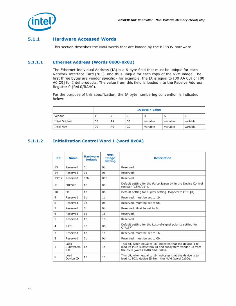
82583V GbE Controller—Non-Volatile Memory (NVM) Map
58
5.1.1 Hardware Accessed Words
This section describes the NVM words that are loaded by the 82583V hardware.
5.1.1.1 Ethernet Address (Words 0x00-0x02)
The Ethernet Individual Address (IA) is a 6-byte field that must be unique for each Network Interface Card (NIC), and thus unique for each copy of the NVM image. The first three bytes are vendor specific - for example, the IA is equal to [00 AA 00] or [00 A0 C9] for Intel products. The value from this field is loaded into the Receive Address Register 0 (RAL0/RAH0).
For the purpose of this specification, the IA byte numbering convention is indicated below:
5.1.1.2 Initialization Control Word 1 (word 0x0A)
IA Byte / Value
Vendor 1 2 3 4 5 6
Intel Original 00 AA 00 variable variable variable
Intel New 00 A0 C9 variable variable variable
Bit Name Hardware Default
NVM Image Setting
Description
15 Reserved 0b 0b Reserved.
14 Reserved 0b 0b Reserved.
13:12 Reserved 00b 00b Reserved.
11 FRCSPD 1b 0b Default setting for the Force Speed bit in the Device Control register (CTRL[11]).
10 FD 1b 0b Default setting for duplex setting. Mapped to CTRL[0].
9 Reserved 1b 1b Reserved, must be set to 1b.
8 Reserved 0b 0b Reserved, must be set to 0b.
7 Reserved 0b 0b Reserved, Must be set to 0b.
6 Reserved 1b 1b Reserved.
5 Reserved 1b 1b Reserved.
4 ILOS 0b 0b Default setting for the Loss-of-signal polarity setting for CTRL[7].
3 Reserved 1b 1b Reserved, must be set to 1b.
2 Reserved 0b 0b Reserved, must be set to 0b.
1Load Subsystem IDs
1b 1bThis bit, when equal to 1b, indicates that the device is to load its PCIe subsystem ID and subsystem vendor ID from the NVM (words 0x0B and 0x0C).
0 Load Device ID 1b 1b This bit, when equal to 1b, indicates that the device is to
load its PCIe device ID from the NVM (word 0x0D).
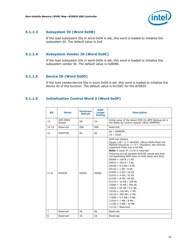
59
Non-Volatile Memory (NVM) Map—82583V GbE Controller
5.1.1.3 Subsystem ID (Word 0x0B)
If the load subsystem IDs in word 0x0A is set, this word is loaded to initialize the subsystem ID. The default value is 0x0.
5.1.1.4 Subsystem Vendor ID (Word 0x0C)
If the load subsystem IDs in word 0x0A is set, this word is loaded to initialize the subsystem vendor ID. The default value is 0x8086.
5.1.1.5 Device ID (Word 0x0D)
If the load vendor/device IDs in word 0x0A is set, this word is loaded to initialize the device ID of the function. The default value is 0x150C for the 82583V.
5.1.1.6 Initialization Control Word 2 (Word 0x0F)
Bit Name Hardware Default
NVM Image Setting
Description
15 APM PME# Enable 0b 1b Initial value of the Assert PME On APM Wakeup bit in
the Wake Up Control register (WUC.APMPME).
14:13 Reserved 00b 00b Reserved.
12 NVMTYPE 0b 0b0b = EEPROM.1b = Flash.
11:8 NVSIZE 0000b 0000b
NVM size [bytes]Equals 128 * 2 ** NVSIZE. (When NVM=Flash the NVSIZE should be >= 9 ‡. Therefore, the minimal supported Flash size is 64 KB).Note: A value of 1111b is reserved.Following are all possible NVSIZE values and their corresponding NVM sizes (in both bytes and bits):0000b = 128 B / 1 Kb.0001b = 256 B / 2 Kb.0010b = 0.5 KB / 4 Kb.0011b = 1 KB / 8 Kb.0100b = 2 KB / 16 Kb.0101b = 4 KB / 32 Kb.0110b = 8 KB / 64 Kb.0111b = 16 KB / 128 Kb.1000b = 32 KB / 256 Kb.1001b = 64 KB / 0.5 Mb.1010b = 128 KB / 1 Mb.1011b = 265 KB / 2 Mb.1100b = 0.5 MB / 4 Mb.1101b = 1 MB / 8 Mb.1110b = 2 MB / 16 Mb.1111b = Reserved.
7 Reserved 0b 0b Reserved.
6 Reserved 1b 1b Reserved.

82583V GbE Controller—Non-Volatile Memory (NVM) Map
60
5.1.1.7 NVM Protected Word 0 - NVP0 (Word 0x10)
5.1.1.8 NVM Protected Word 1 - NVP1 (Word 0x11)
Bit Name Hardware Default
NVM Image Setting
Description
5 Reserved 0b 0b Reserved.
4 Reserved 1b 1b Reserved.
3 Reserved 1b 1b Reserved.
2 Reserved 0b 0b Reserved.
1 Reserved 0b 0b Reserved.
0 Reserved 0b 0b Reserved.
Bit Name Hardware Default
NVM Image Setting
Description
15:8 Reserved 0x0 0x0 Reserved.
7:0 Reserved 0x0 0x0 Reserved.
Bit Name Hardware Default
NVM Image Setting
Description
15:8 FSECER 0x20 0x20Defines the instruction code for the block erase used by the 82583V. The erase block size is defined by the SECSIZE field in address 0x12.
7:1 Reserved 0x0 0x0 Reserved.
0 RAM_PWR_SAVE_EN 1b 1b When set to 1b, enables reducing power consumption by
clock gating the 82583V RAMs.

61
Non-Volatile Memory (NVM) Map—82583V GbE Controller
5.1.1.9 NVM Protected Word 2 - NVP2 (Word 0x12)
5.1.1.10 Extended Configuration Word 1 (Word 0x14)
5.1.1.11 Extended Configuration Word 2 (Word 0x15)
Bit Name Hardware Default
NVM Image Setting
Description
15:8 SIGN 0x7E 0x7E
SignatureThe 8-bit Signature field indicates to the device that there is a valid NVM present. If the Signature field does not equal 0x7E then the default values are used for the device configuration.
7 Reserved 0b 0b Reserved, must be set to 0b.
6 Reserved 0b 1b Reserved.
5 Reserved 0b 1b Reserved.
4 Reserved 0b 1b Reserved.
3:2 SECSIZE 01b 01b
The SECSIZE defines the Flash sector erase size as follows:00b = 256 bytes.01b = 4 KB.10b = Reserved.11b = Reserved.
1:0 Reserved 00b 00b Reserved, must be set to 00b.
Bit Name Hardware Default
NVM Image Setting
Description
15:13 Reserved 100b 100b Reserved.
12 Reserved 0b 1b Reserved.
11:0 Reserved 0x0 0x0 Reserved.
Bit Name Hardware Default
NVM Image Setting
Description
15:8 Reserved 0x0 0x0 Reserved.
7 Reserved 1b 1b Reserved.
6 Reserved 1b 1b Reserved.
5 Reserved 0b 0b Reserved.
4 Reserved 0b 0b Reserved.
3 Reserved 1b 1b Reserved.
2 Reserved 0b 0b Reserved.
1 Reserved 0b 0b Reserved.
0 Reserved 0b 0b Reserved.

82583V GbE Controller—Non-Volatile Memory (NVM) Map
62
5.1.1.12 Extended Configuration Word 3 (Word 0x16)
5.1.1.13 PCIe Electrical Idle Delay (Word 0x17)
5.1.1.14 PCIe Init Configuration 1 Word (Word 0x18)
Bit Name Hardware Default
NVM Image Setting
Description
15:8 Reserved 0x0 0x0 Reserved.
7:0 Reserved 0x0 0x0 Reserved.
Bit Name Hardware Default
NVM Image Setting
Description
15:14 Reserved 00b 00b Reserved.
13 Reserved 1b 1b Reserved.
12:8 Reserved 0x7 0x7 Reserved.
7:3 Reserved 0x0 0x0 Reserved.
2 Reserved 1b 1b Reserved.
1 Reserved 0b 0b Reserved.
0 Reserved 0b 0b Reserved.
Bit Name Hardware Default NVM Image Setting Description
15 Reserved 0b 0b Reserved, must be set to 0b.
14:12 L1_Act_Ext_Latency 110b (32μs-64 μs) 110b (32 μs-64 μs) L1 active exit latency for the configuration space.
11:9 L1_Act_Acc_Latency 110b (32 μs-64 μs) 110b (32 μs-64 μs) L1 active acceptable latency for the configuration space.
8:6 L0s_Acc_Latency 011b (512 ns) 011b (512 ns) L0s acceptable latency for the configuration space.
5:3 L0s_Se_Ext_Latency 001b 001b
L0s exit latency for active state power management (separated reference clock) – (latency between 64 ns – 128 ns).
2:0 L0s_Co_Ext_Latency 001b 001b
L0s exit latency for active state power management (common reference clock) – (latency between 64 ns – 128 ns).
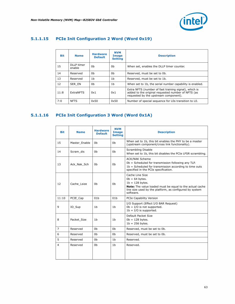
63
Non-Volatile Memory (NVM) Map—82583V GbE Controller
5.1.1.15 PCIe Init Configuration 2 Word (Word 0x19)
5.1.1.16 PCIe Init Configuration 3 Word (Word 0x1A)
Bit Name Hardware Default
NVM Image Setting
Description
15 DLLP timer enable 0b 0b When set, enables the DLLP timer counter.
14 Reserved 0b 0b Reserved, must be set to 0b.
13 Reserved 1b 1b Reserved, must be set to 1b.
12 SER_EN 0b 1b When set to 1b, the serial number capability is enabled.
11:8 ExtraNFTS 0x1 0x1Extra NFTS (number of fast training signal), which is added to the original requested number of NFTS (as requested by the upstream component).
7:0 NFTS 0x50 0x50 Number of special sequence for L0s transition to L0.
Bit Name Hardware Default
NVM Image Setting
Description
15 Master_Enable 0b 0b When set to 1b, this bit enables the PHY to be a master (upstream component/cross link functionality).
14 Scram_dis 0b 0bScrambling DisableWhen set to 1b, this bit disables the PCIe LFSR scrambling.
13 Ack_Nak_Sch 0b 0b
ACK/NAK Scheme0b = Scheduled for transmission following any TLP.1b = Scheduled for transmission according to time outs specified in the PCIe specification.
12 Cache_Lsize 0b 0b
Cache Line Size0b = 64 bytes.1b = 128 bytes.Note: The value loaded must be equal to the actual cache line size used by the platform, as configured by system software.
11:10 PCIE_Cap 01b 01b PCIe Capability Version
9 IO_Sup 1b 1bI/O Support (Effect I/O BAR Request)0b = I/O is not supported.1b = I/O is supported.
8 Packet_Size 1b 1bDefault Packet Size0b = 128 bytes.1b = 256 bytes.
7 Reserved 0b 0b Reserved, must be set to 0b.
6 Reserved 0b 0b Reserved, must be set to 0b.
5 Reserved 0b 1b Reserved.
4 Reserved 0b 1b Reserved.

82583V GbE Controller—Non-Volatile Memory (NVM) Map
64
5.1.1.17 PCIe Control (Word 0x1B)
Bit Name Hardware Default
NVM Image Setting
Description
3:2 Act_Stat_PM_Sup 0x3 0x3
Determines support for Active State Link Power Management (ASLPM). Loaded into the PCIe Active State Link PM Support register.Note: Changing the default value of this field might affect certain power savings features of the 82583V. However, in some applications, it might be necessary to change this value as explained in the Intel® 82583V Gigabit Ethernet Controller Specification Update. Please refer to Erratum #9 for more details.
1 Slot_Clock_Cfg 1b 1b When set, the 82583V uses the PCIe reference clock supplied on the connector (for add-in solutions).
0Loop back polarity inversion
0b 0b
Check Polarity Inversion in Loop-Back Master EntryDuring normal operation polarity is adjusted during link up. When this bit is set, the receiver re-checks the polarity of Rx-data and then inverts it accordingly, when entering a near-end loopback. When cleared, polarity is not re-checked after link up.
Bit Name Hardware Default
NVM Image Setting
Description
15 PCIE_RX_Valid 0b 0b Force receiver presence detection. When set, the 82583V
overrides the receiver (partner) detection status.
14 Latency_To_Enter_L1 1b 1b
MSB [2] of period in L0s state before transitioning into an L1 state (lower bits are in bits [1:0].Recommended setting: {14, 1:0} = 011b – 32 μs.
13 PCIE Down Reset Disable 0b 0b Disable a core reset when the PCIe link goes down.
12 PCIE_LTSSM 0b 0bWhen cleared, LTSSM complies with the SlimPIPE specification (power mode transition). When set, LTSSM behaves as in previous generations.
11 Good Recovery 0b 0b
When this bit is set, the LTSSM recovery states always progress towards link up (force a good recovery when a recovery occurs).
10 Leaky Bucket Disable 1b 1b
Disable leaky bucket mechanism in the PCIe PHY. Disabling this mechanism holds the link from going to recovery retrain in case of disparity errors.
9:7 Reserved 0x0 0x0 Reserved.
6 Reserved 0b 0b Reserved.
5 L2 Disable 0b 0b Disable the link from entering L2 state.
4 Skip Disable 0b 0b Disable skip symbol insertion in the elastic buffer.

65
Non-Volatile Memory (NVM) Map—82583V GbE Controller
3 Reserved 0b 1b Reserved.
2 Electrical IDLE 0b 0b
Electrical Idle MaskIf set to 1b, disables the check for illegal electrical idle sequence (such as, eidle ordered set without common mode and vise versa), and accepts any of them as the correct eidle sequence.Note: The specification can be interpreted so that idle ordered set is sufficient for transition to power management states. The use of this bit allows an acceptance of such interpretation and avoids the possibility of correct behavior to be understood as illegal sequences.
1:0 Latency_To_Enter_L1 0x3 0x3
Period in L0s state before transitioning into an L1 state bits [1:0].00b = 64 μs.01b = 256 μs.10b = 1 ms.11b = 4 ms.
Bit Name Hardware Default
NVM Image Setting
Description

82583V GbE Controller—Non-Volatile Memory (NVM) Map
66
5.1.1.18 LED 1 Configuration Defaults/PHY Configuration (Word 0x1C)
Bit Name Hardware Default
NVM Image Setting
Description
15 Reserved 0b 0b Reserved.
14 Giga Disable 0b 0b When set, 1000 Mb/s operation is disabled in all power modes.
13 Reserved 1b 1b Reserved.
12 Class AB 0b 0b
When set, the PHY operates in class A mode instead of class B mode. This mode only applies for 1000BASE-T operation. 10BASE-T and 100BASE-T operation continue to run in Class B mode by default, regardless of this signal value.
11 Disable 1000 in non-D0a 1b 1b Disables 1000 Mb/s operation in non-D0a states.
10 LPLU 1b 1bLow Power Link UpEnables decrease in link speed in non-D0a states when the power policy and power management state dictate so.
9 D0LPLU 0b 0bD0 Low Power Link UpEnables decrease in link speed in D0a state when the power policy and power management state dictate so.
8 Reserved 1b 1b Reserved.
7 LED1 Blink 1b 1bInitial Value of LED1_BLINK Field0b = Non-blinking
6 LED1 Invert 0b 0bInitial Value of LED1_IVRT Field0b = Active-low output
5 LED1 Blink Mode 0b 0b
LED1 Blink Mode0b = Blinks at 200 ms on and 200 ms off.1b = Blinks at 83 ms on and 83 ms off.
4 Reserved 0b 0b Reserved.
3:0 LED1 Mode 0x4 0x4Initial value of the LED1_MODE field specifying what event/state/pattern is displayed on the LED1 (ACTIVITY) output. A value of 0011b (0x3) indicates the ACTIVITY state.

67
Non-Volatile Memory (NVM) Map—82583V GbE Controller
5.1.1.19 Reserved Word 0x1D
5.1.1.20 Device Rev ID (Word 0x1E)
Bit Name Hardware Default
NVM Image Setting
Description
15:9 Reserved 0x0 0x0 Reserved.
8 Reserved 1b 1b Reserved.
7 Reserved 0b 0b Reserved.
6 Reserved 0b 0b Reserved.
5 Reserved 0b 0b Reserved.
4:0 Reserved 0x0 0x0 Reserved.
Bit Name Hardware Default
NVM Image Setting
Description
15 Reserved 0b 1b Reserved.
14 Reserved 1b 1b Reserved.
13 Reserved 0b 1b Reserved.
12 Reserved 0b 1b Reserved.
11 Reserved 0b 0b Reserved.
10 Reserved 0b 0b Reserved.
9 Reserved 1b 0b Reserved.
8 Reserved 1b 0b Reserved.
7:0 Reserved 0x0 0x0 Reserved.

82583V GbE Controller—Non-Volatile Memory (NVM) Map
68
5.1.1.21 LED 0, 2 Configuration Defaults (Word 0x1F)
Bit Name Hardware Default
NVM Image Setting
Description
15 LED2 Blink 0b 0bInitial Value of LED2_BLINK Field0b = Non-blinking.
14 LED2 Invert 0b 0bInitial Value of LED2_IVRT Field0b = Active-low output.
13 LED2 Blink Mode 0b1 0b1
LED2 Blink Mode0b = Blinks at 200 ms on and 200 ms off.1b = Blinks at 83 ms on and 83 ms off.
12 Reserved 0b 0b Reserved.
11:8 LED2 Mode 0x7 0x7
Initial value of the LED2_MODE field specifying what event/state/pattern is displayed on LED2 (LINK_100) output. A value of 0110b (0x6) causes this to indicate 100 Mb/s operation.
7 LED0 Blink 0b 0bInitial Value of LED0_BLINK Field0b = Non-blinking.
6 LED0 Invert 0b 0bInitial Value of LED0_IVRT Field0b = Active-low output.
5 LED0 Blink Mode 0b1
1. These bits are read from the NVM.
0b1LED0 Blink Mode0b = Blinks at 200 ms on and 200 ms off.1b = Blinks at 83 ms on and 83 ms off.
4 Reserved 0b 0b Reserved, set to 0b.
3:0 LED0 Mode 0x6 0x6Initial value of the LED0_MODE field specifying what event/state/pattern is displayed on the LED0 (LINK_UP) output. A value of 0010b (0x2) causes this to indicate LINK_UP state.

69
Non-Volatile Memory (NVM) Map—82583V GbE Controller
5.1.1.22 Flash Parameters - FLPAR (Word 0x20)
5.1.1.23 Flash LAN Address - FLANADD (Word 0x21)
Bit Name Hardware Default
NVM Image Setting
Description
15:8 FDEVER 0x60 0x60Defines the instruction code for the Flash device erase. A value of 0x00 means that the device does not support the device erase.
7:6 Reserved 0x0 0x0 Reserved.
5 FLSSTn 0b 0b
SST Flash NotWhen set to 0b, indicates an SST FLASH type: write access to the Flash is limited to 1 byte at a time and it is required to clear write protection at power up. When set to 1b, burst write access to the Flash is enabled up to 256 bytes and it is not required to clear write protection at power up.
4 LONGC 0b 0b
Very Long Cycle IndicationWhen set to 1b, the LONGC indicates to the 82583V that a Flash write instruction is considered a very long instruction. When set to '0b, the LONGC indicates that a write cycle to the Flash is not considered a very long cycle.
3:0 Reserved 0x0 0x0 Reserved.
Bit Name Hardware Default
NVM Image Setting
Description
15 DISLFB 0b 0b 1b = Disables the LAN Flash BAR.
14:12 LANSIZE 0x0 0x0 LAN boot expansion window size = 2 KB * 2 ** LANSIZE.
11:8 LBADD 0x0 0x0
LAN Flash AddressDefines the location of the LAN boot expansion ROM in the physical Flash device as defined in the following equation:Word Address = 4 KB * (LBADD + PEND).
7 DISLEXP 0b 1b 1b = Disables the LAN expansion boot ROM BAR.
6:1 Reserved 0x0 0x0 Reserved.
0 Reserved 0b 0b Reserved.
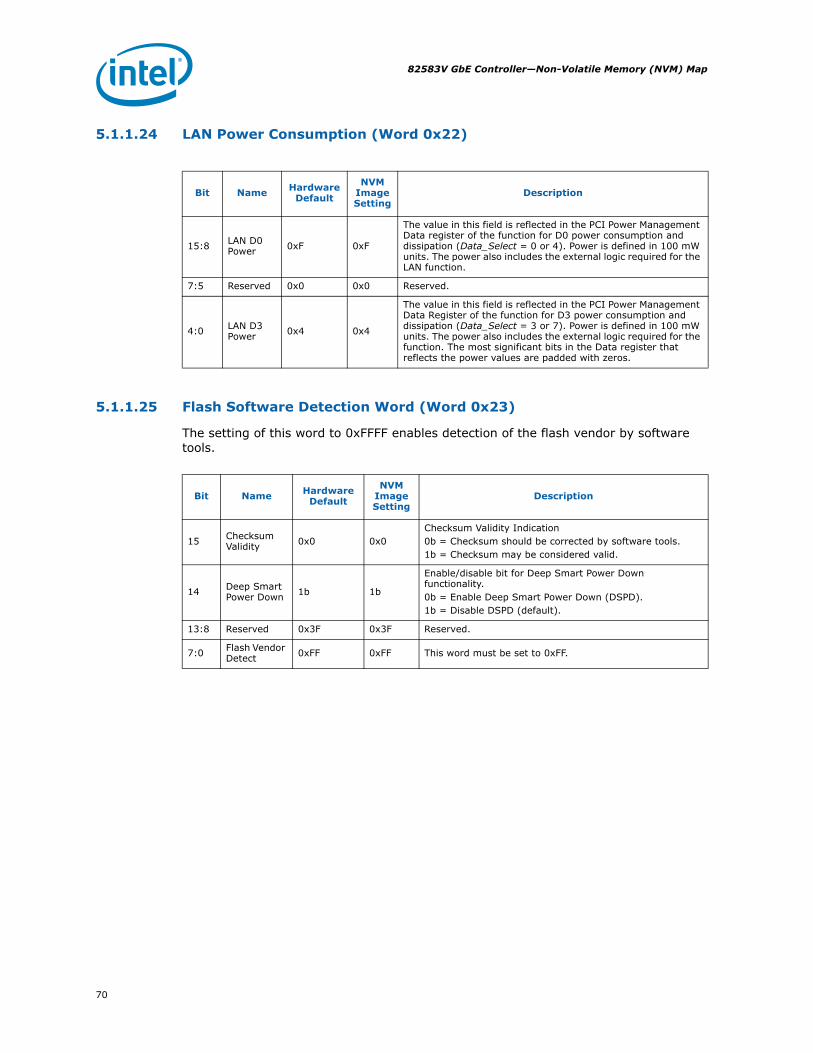
82583V GbE Controller—Non-Volatile Memory (NVM) Map
70
5.1.1.24 LAN Power Consumption (Word 0x22)
5.1.1.25 Flash Software Detection Word (Word 0x23)
The setting of this word to 0xFFFF enables detection of the flash vendor by software tools.
Bit Name Hardware Default
NVM Image Setting
Description
15:8 LAN D0 Power 0xF 0xF
The value in this field is reflected in the PCI Power Management Data register of the function for D0 power consumption and dissipation (Data_Select = 0 or 4). Power is defined in 100 mW units. The power also includes the external logic required for the LAN function.
7:5 Reserved 0x0 0x0 Reserved.
4:0 LAN D3 Power 0x4 0x4
The value in this field is reflected in the PCI Power Management Data Register of the function for D3 power consumption and dissipation (Data_Select = 3 or 7). Power is defined in 100 mW units. The power also includes the external logic required for the function. The most significant bits in the Data register that reflects the power values are padded with zeros.
Bit Name Hardware Default
NVM Image Setting
Description
15 Checksum Validity 0x0 0x0
Checksum Validity Indication0b = Checksum should be corrected by software tools.1b = Checksum may be considered valid.
14 Deep Smart Power Down 1b 1b
Enable/disable bit for Deep Smart Power Down functionality.0b = Enable Deep Smart Power Down (DSPD).1b = Disable DSPD (default).
13:8 Reserved 0x3F 0x3F Reserved.
7:0 Flash Vendor Detect 0xFF 0xFF This word must be set to 0xFF.

71
Non-Volatile Memory (NVM) Map—82583V GbE Controller
5.1.1.26 Initialization Control 3 (Word 0x24)
Bit Name Hardware Default
NVM Image Setting
Description
15 Reserved 0b 0b Reserved.
14 Reserved 1b 1b Reserved.
13 Reserved 1b 0b Reserved.
12 Reserved 0b 0b Reserved.
11 Reserved 1b 1b Reserved.
10 APM Enable 0b 1bInitial value of Advanced Power Management Wake Up Enable in the Wake Up Control (WUC.APME) register. Mapped to CTRL[6] and to WUC[0].
9 Reserved 0b 1b Reserved.
8 Reserved 0b 1b Reserved.
7:1 Reserved 0x0 0x0 Reserved.
0 No_Phy_Rst 1b 1b
No PHY ResetWhen set to 1b, this bit prevents the PHY reset signal and the power changes reflected to the PHY according to the MANC.Keep_PHY_Link_Up value.

82583V GbE Controller—Non-Volatile Memory (NVM) Map
72
5.1.2 Software Accessed Words
5.1.2.1 Compatibility Fields (Words 0x03 - 0x07)
This section describes the meaningful NVM words in the basic configuration space that are used by software at word addresses 0x03 to 0x07.
5.1.2.2 Compatibility Bytes (Word 0x03)
5.1.2.3 Compatibility Bytes (Word 0x04)
Bit Name Hardware Default
NVM Image Setting
Description
15:13 Reserved 000b 000b Reserved.
12 Reserved 0b 0b Reserved.
11 LOM 0b 0bLOM or NIC0b = NIC.1b = LOM.
10 Server NIC 1b 1bServer NIC0b = Client.1b = Server.
9 Client NIC 1b 0bClient NIC0b = Server.1b = Client.
8 Retail Card 0b 0bRetail Card0b = Retail.1b = OEM.
7:6 Reserved 00b 00b Reserved.
5 Reserved 1b 1b Reserved.
4 Reserved 0b 0b Reserved
3 Reserved 0b 0b Reserved.
2 PCI Bridge 1b 0bPCI Bridge NOT Present0b = PCI bridge NOT present.1b = PCI bridge present.
1:0 Reserved 00b 00b Reserved.
Bit Name Hardware Default
NVM Image Setting
Description
15:12 Reserved 0xF 0xF Reserved.
11:8 LED 2 Control 0x7 0x7 Control for LED 2 - LINK_1000.
7:4 LED 1Control 0x4 0x4 Control for LED 1 - LINK/ACTIVITY.
3:0 LED 0 Control 0x6 0x6 Control for LED 0 - LINK_100.
73
Non-Volatile Memory (NVM) Map—82583V GbE Controller
5.1.2.3.1 Compatibility Byte (Word 0x05)
5.1.2.3.2 Compatibility Bytes (Word 0x06 - 0x07)
5.1.2.4 PBA Number (Word 0x08 and 0x09)
The nine-digit Printed Board Assembly (PBA) number used for Intel manufactured Network Interface Cards (NICs) is stored in the EEPROM.
Note that through the course of hardware ECOs, the suffix field is incremented. The purpose of this information is to enable customer support (or any user) to identify the revision level of a product.
Network driver software should not rely on this field to identify the product or its capabilities.
Current PBA numbers have exceeded the length that can be stored as hex values in these two words. For these PBA numbers the high word is a flag (0xFAFA) indicating that the PBA is stored in a separate PBA block. The low word is a pointer to a PBA block.
The PBA block is pointed to by word 0x09.
The PBA block contains the complete PBA number including the dash and the first digit of the 3-digit suffix. For example:
Older PBA numbers starting with (A,B,C,D,E) are stored directly in words 0x08 and 0x09. The dash itself is not stored nor is the first digit of the 3-digit suffix, as it is always 0b for relevant products.
Bits Name Hardware Default
NVM Image Setting
Description
15:0 Reserved 0x10A0 0x10A0 Reserved.
Bits Name Hardware Default
NVM Image Setting
Description
15:0 Reserved 0xFFFF 0xFFFF Reserved.
PBA Number Word 0x08 Word 0x09
G23456-003 FAFA Pointer to PBA Block
Word Offset Description End UserReserved
0x0 Length in words of the PBA block (default 0x6). No
0x1 ... 0x5 PBA number stored in hexadecimal ASCII values. No
PBA Number Word Offset 0
Word Offset 1
Word Offset 2
Word Offset 3
Word Offset 4
Word Offset 5
G23456-003 0006 4732 3334 3536 2D30 3033

82583V GbE Controller—Non-Volatile Memory (NVM) Map
74
5.1.2.5 PXE Words (Words 0x30:0x3E)
Words 0x30 through 0x3E are reserved for software and are used by IBA/PXE software.
5.1.2.6 iSCSI Boot Configuration Start Address (Word 0x3D)
5.1.2.6.1 Boot Agent Main Setup Options (Word 0x30)
The boot agent software configuration is controlled by the NVM with the main setup options stored in word 0x30. These options are those that can be changed by using the Control-S setup menu or by using the IBA Intel Boot Agent utility. Note that these settings only apply to Boot Agent software.
PBA Number Byte 1 Byte 2 Byte 3 Byte 4
123456-003 12 34 56 03
Bit Name Default Description
15:0 Address 0x0 NVM word address of the iSCSI boot configuration structure starting point.

75
Non-Volatile Memory (NVM) Map—82583V GbE Controller
Table 19. Boot Agent Main Setup Options
Bit Name Hardware Default
NVM Image Setting
Description
15:13 Reserved 000b Reserved, set to 0x0.
12 FDP 0bForce Full Duplex.Set this bit to 0b for half duplex and 1b for full duplex.Note that this bit is a don’t care unless bits 10 and 11 are set.
11:10 FSP 00b
Force Speed.These bits determine speed.01b = 10 Mb/s.10b = 100 Mb/s.11b = Not allowed.All zeros indicate auto-negotiate (the current bit state).Note that bit 12 is a don’t care unless these bits are set.
9 Reserved 0bReservedSet this bit to 0b.
8 DSM 1b 1bDisplay Setup Message.If this bit is set to 1b, the "Press Control-S" message appears after the title message.
7:6 PT 00b
Prompt Time. These bits control how long the "Press Control-S" setup prompt message appears, if enabled by DIM.00b = 2 seconds (default).01b = 3 seconds.10b = 5 seconds.11b = 0 seconds.Note that the Ctrl-S message does not appear if 0 seconds prompt time is selected.
5 Reserved 0b Reserved
4:3 DBS 00b
Default Boot Selection. These bits select which device is the default boot device. These bits are only used if the agent detects that the BIOS does not support boot order selection or if the MODE field of word 0x31 is set to MODE_LEGACY.00b = Network boot, then local boot.01b = Local boot, then network boot.10b = Network boot only.11b = Local boot only.
2 Reserved 0b Reserved
1:0 PS 00b
Protocol Select. These bits select the boot protocol.00b = PXE (default value).01b = Reserved.Other values are undefined.

82583V GbE Controller—Non-Volatile Memory (NVM) Map
76
5.1.2.6.2 Boot Agent Configuration Customization Options (Word 0x31)
Word 0x31 contains settings that can be programmed by an OEM or network administrator to customize the operation of the software. These settings cannot be changed from within the Control-S setup menu or the IBA Intel Boot Agent utility. The lower byte contains settings that would typically be configured by a network administrator using the Intel Boot Agent utility; these settings generally control which setup menu options are changeable. The upper byte are generally settings that would be used by an OEM to control the operation of the agent in a LOM environment, although there is nothing in the agent to prevent their use on a NIC implementation.
Table 20. Boot Agent Configuration Customization Options (Word 0x31)
Bit Name Hardware Default
NVM Image Setting
Description
15:14 SIG 11bSignatureSet these bits to 11b to indicate valid data.
13:12 Reserved 00b Reserved, must be set to 00b.
11 0b Continuous Retry Disabled (0b default).
10:8 MODE 000b
Selects the agent's boot order setup mode. This field changes the agent's default behavior in order to make it compatible with systems that do not completely support the BBS and PnP Expansion ROM standards. Valid values and their meanings are:000b = Normal behavior. The agent attempts to detect BBS and PnP Expansion ROM support as it normally does.001b = Force Legacy mode. The agent does not attempt to detect BBS or PnP Expansion ROM supports in the BIOS and assumes the BIOS is not compliant. The BIOS boot order can be changed in the Setup Menu.010b = Force BBS mode. The agent assumes the BIOS is BBS-compliant, even though it may not be detected as such by the agent's detection code. The BIOS boot order CANNOT be changed in the Setup Menu.011b = Force PnP Int18 mode. The agent assumes the BIOS allows boot order setup for PnP Expansion ROMs and hooks interrupt 18h (to inform the BIOS that the agent is a bootable device) in addition to registering as a BBS IPL device. The BIOS boot order CANNOT be changed in the Setup Menu.100b = Force PnP Int19 mode. The agent assumes the BIOS allows boot order setup for PnP Expansion ROMs and hooks interrupt 0x19 (to inform the BIOS that the agent is a bootable device) in addition to registering as a BBS IPL device. The BIOS boot order CANNOT be changed in the Setup Menu.101b = Reserved for future use. If specified, treated as value 000b.110b = Reserved for future use. If specified, treated as value 000b.111b = Reserved for future use. If specified, treated as value 000b.
7:6 Reserved 00b Reserved, must be set to 00b.
5 DFU 0b
Disable Flash UpdateIf set to 1b, no updates to the Flash image using PROSet is allowed.The default for this bit is 0b; allow Flash image updates using PROSet.

77
Non-Volatile Memory (NVM) Map—82583V GbE Controller
5.1.2.6.3 Boot Agent Configuration Customization Options (Word 0x32)
Word 0x32 is used to store the version of the boot agent that is stored in the Flash image. When the Boot Agent loads, it can check this value to determine if any first-time configuration needs to be performed. The agent then updates this word with its version. Some diagnostic tools to report the version of the Boot Agent in the Flash also read this word. This word is only valid if the PPB is set to 0b. Otherwise the contents might be undefined.
Table 21. Boot Agent Configuration Customization Options (Word 0x32)
4 DLWS 0b
Disable Legacy Wakeup SupportIf set to 1b, no changes to the Legacy OS Wakeup Support menu option is allowed.The default for this bit is 0b; allow Legacy OS Wakeup Support menu option changes.
3 DBS 0b
Disable Boot SelectionIf set to 1b, no changes to the boot order menu option is allowed.The default for this bit is 0b; allow boot order menu option changes.
2 DPS 0b
Disable Protocol SelectIf set to 1b, no changes to the boot protocol is allowed.The default for this bit is 0b; allow changes to the boot protocol.
1 DTM 0b
Disable Title MessageIf set to 1b, the title message displaying the version of the boot agent is suppressed; the Control-S message is also suppressed. This is for OEMs who do not want the boot agent to display any messages at system boot.The default for this bit is 0b; allow the title message that displays the version of the boot agent and the Control-S message.
0 DSM 0b
Disable Setup MenuIf set to 1b, no invoking the setup menu by pressing Control-S is allowed. In this case, the EEPROM can only be changed via an external program.The default for this bit is 0b; allow invoking the setup menu by pressing Control-S.
Bit Name Hardware Default
NVM Image Setting
Description
Bit Name Hardware Default
NVM Image Setting
Description
15:12 MAJOR 0x1 0x1 PXE boot agent major version.
11:8 MINOR 0x2 0x2 PXE boot agent minor version.
7:0 BUILD 0x28 0x1C PXE boot agent build number..

82583V GbE Controller—Non-Volatile Memory (NVM) Map
78
5.1.2.6.4 IBA Capabilities (Word 0x33)
Word 0x33 is used to enumerate the boot technologies that have been programmed into the Flash. It is updated by IBA configuration tools and is not updated or read by IBA.
Table 22. IBA Capabilities
5.1.2.7 Virtual MAC Data Pointer (Word 0x37)
5.1.2.8 Vital Product Data Pointer (VDP) (Word 0x2F)
Bit Name Hardware Default
NVM Image Setting
Description
15:14 SIG 11b
SignatureThese bits must be set to 11b to indicate that this word has been programmed by the agent or other configuration software.
13:5 Reserved 0x0 Reserved, must be set to 0x0.
4 0b 0b iSCSI boot capability not present.
3 EFI 0b 0bEFI EBC capability is present in Flash.0b = The EFI code is not present.1b = The EFI code is present.
2 Reserved 1b Reserved, set to 1b.
1 UNDI 1b 1bPXE/UNDI capability is present in Flash.1b = The PXE base code is present.0b = The PXE base code is not present.
0 BC 0b 1bPXE base code is present in Flash.0b = The PXE base code is present.1b = The PXE base code is not present.
Bit Name Hardware Default
NVM Image Setting
Description
15:0 0x0 0xFFFF Virtual MAC Data Pointer.
Bit Name Hardware Default
NVM Image Size
Description
15:0 VDP 0xFFFF Reserved, set to 0xFFFF.

79
Non-Volatile Memory (NVM) Map—82583V GbE Controller
5.1.2.9 iSCSI Boot Configuration Start Address (Word 0x3D)
5.1.2.10 Checksum Word Calculation (Word 0x3F)
The checksum word (0x3F) is used to ensure that the base NVM image is a valid image. The value of this word should be calculated such that after adding all the words (0x00-0x3F), including the checksum word itself, the sum should be 0xBABA. The initial value in the 16-bit summing register should be 0x0000 and the carry bit should be ignored after each addition.
Note: Hardware does not calculate the word 0x3F checksum during an NVM write or read. It must be calculated by software independently and included in the NVM write data. This field is provided strictly for software verification of NVM validity. All hardware configuration based on word 0x00-0x3F content is based on the validity of the Signature field of the NVM.
Bit Name Hardware Default
NVM Image Setting
Description
15:0 Address 0x0 0x120 NVM word address of the iSCSI boot configuration structure starting point.

82583V GbE Controller—Interconnects
80
6.0 Interconnects
6.1 PCIePCIe is a third generation I/O architecture that enables cost competitive, next generation I/O solutions providing industry leading price/performance and feature richness. It is an industry-driven specification.
PCIe defines a basic set of requirements that comprehends the majority of the targeted application classes. High-end application requirements such as Enterprise class servers and high-end communication platforms are delivered by a set of advanced extensions that compliment the baseline requirements.
To guarantee headroom for future applications of PCIe, a software-managed mechanism for introducing new, enhanced capabilities in the platform is provided. Figure 23 shows the PCIe architecture.
Figure 23. PCIe Stack Structure
The PCIe physical layer consists of a differential transmit pair and a differential receive pair. Full-duplex data on these two point-to-point connections is self-clocked such that no dedicated clock signals are required.
Note: The bandwidth of this interface increases linearly with frequency.
2.5+ 2.5+ GbGb/s/s
PCI.sys CompliantPCI.sys Compliant
Configurable widths 1 .. 32Configurable widths 1 .. 32
Preserve Driver ModelPreserve Driver Model
Config/OS
S/W
Protocol
Link
Physical
Common Base ProtocolCommon Base Protocol
Advanced Advanced XtensionsXtensions
Physical(electrical
Mechanical)
Point to point, serial, differential,Point to point, serial, differential,hothot--plug, interplug, inter--op op formfactorsformfactors

81
Interconnects—82583V GbE Controller
A packet is the fundamental unit of information exchange and the protocol includes a message space to replace the number of side-band signals found on many of today’s buses. This movement of hard-wired signals from the physical layer to messages within the transaction layer enables easy and linear physical layer width expansion for increased bandwidth.
The common base protocol uses split transactions along with several mechanisms that are included to eliminate wait states and to optimize the reordering of transactions to further improve system performance.
6.1.1 Architecture, Transaction, and Link Layer Properties
• Split transaction, packet-based protocol• Common flat address space for load/store access (such as a PCI addressing
model):— Memory address space of 32 bits to enable compact packet header (must be
used to access addresses below 4 GB)— Memory address space of 64 bits using extended packet header
• Transaction layer mechanisms:— PCI-X style relaxed ordering— Optimizations for no-snoop transactions
• Credit-based flow control• Packet sizes/formats:
— Maximum packet size supports 128- and 256-byte data payload— Maximum read request size of 4 KB
• Reset/initialization:— Frequency/width/profile negotiation performed by hardware
• Data integrity support:— Using CRC-32 for transaction layer packets
• Link layer retry for recovery following error detection:— Using CRC-16 for link layer messages
• No retry following error detection:— 8b/10b encoding with running disparity
• Software configuration mechanism:— Uses PCI configuration and bus enumeration model— PCIe-specific configuration registers mapped via PCI extended capability
mechanism• Baseline messaging:
— In-band messaging of formerly side-band legacy signals (such as interrupts)— System-level power management supported via messages
• Power Management (PM):— Full PCI PM support— Wake capability from D3cold state— Compliant with ACPI 2.0, PCI PM software model— Active state power management (transparent to software including ACPI)

82583V GbE Controller—Interconnects
82
6.1.1.1 Physical Interface Properties
• Point to point interconnect— Full-duplex; no arbitration
• Signaling technology: — Low voltage differential— Embedded clock signaling using 8b/10b encoding scheme
• Serial frequency of operation: 2.5 GHz. • Interface width of one lane per direction• DFT and DFM support for high volume manufacturing
6.1.1.2 Advanced Extensions
PCIe defines a set of optional features to enhance platform capabilities for specific usage modes. The 82583V supports the following optional features:
• Extended error reporting – messaging support to communicate multiple types/severity of errors
• Serial number
6.1.2 General Functionality
• Native/legacy:— The PCIe capability register states the device/port type.— The 82583V is a native device by default.
• Locked transactions:— The 82583V does not support locked requests as a target or master.
• End to End CRC (ECRC):— Not supported by the 82583V
6.1.3 Transaction Layer
The upper layer of the PCIe architecture is the transaction layer. The transaction layer connects to the 82583V’s core using an implementation-specific protocol. Through this core-to-transaction-layer protocol, the application-specific parts of the 82583V interact with the PCIe subsystem and transmit and receive requests to or from the remote PCIe agent, respectively.
6.1.3.1 Transaction Types Received by the Transaction Layer
Table 25. Transaction Types at the Rx Transaction Layer
Transaction Type FC Type Tx Later Reaction
Hardware Should Keep Data From Original Packet For Client
Configuration Read Request NPH CPLH + CPLD Requester ID, TAG, Attribute Configuration space
Configuration Write Request
NPH + NPD CPLH Requester ID, TAG, Attribute Configuration space
Memory Read Request NPH CPLH + CPLD Requester ID, TAG, Attribute CSR

83
Interconnects—82583V GbE Controller
Flow control types:• PH - Posted request headers• PD - Posted request data payload• NPH - Non-posted request headers• NPD - Non-posted request data payload• CPLH - Completion headers• CPLD - Completion data payload
6.1.3.2 Transaction Types Initiated by The 82583V
Table 26. Transaction Types at the Tx Transaction Layer
6.1.3.3 Message Handling by The 82583V (as a Receiver)
Message packets are special packets that carry a message code.
The upstream device transmits special messages to the 82583V by using this mechanism.
The transaction layer decodes the message code and responds to the message accordingly.
Memory Write Request
PH + PD
- - CSR
I/O Read Request NPH CPLH + CPLD Requester ID, TAG, Attribute CSR
I/O Write Request NPH + NPD CPLH Requester ID, TAG, Attribute CSR
Read Completions CPLH + CPLD - - DMA
Message PH - - Message Unit / INT / PM / Error Unit
Transaction Type FC Type Tx Later Reaction
Hardware Should Keep Data From Original Packet For Client
Transaction Type Payload Size FC Type From Client
Configuration Read Request Completion Dword CPLH + CPLD Configuration space
Configuration Write Request Completion - CPLH Configuration space
I/O Read Request Completion Dword CPLH + CPLD CSR
I/O Write Request Completion - CPLH CSR
Read Request Completion Dword/Qword CPLH + CPLD CSR
Memory Read Request - NPH DMA
Memory Write Request <= MAX_PAYLOAD_SIZE1
1. The MAX_PAYLOAD_SIZE supported is loaded from the NVM (either 128 bytes or 256 bytes). EffectiveMAX_PAYLOAD_SIZE is according to configuration space register.
PH + PD DMA
Message - PH Message Unit / INT / PM / Error Unit

82583V GbE Controller—Interconnects
84
Table 27. Supported Message in The 82583V (As a Receiver)
6.1.3.4 Message Handling by The 82583V (As a Transmitter)
The transaction layer is also responsible for transmitting specific messages to report internal/external events (such as interrupts and PMEs).
Table 28. Supported Message in The 82583V (As a Transmitter)
Message code [7:0]
Routing r2r1r0 Message Device’s Later Response
0x14 100 PM_Active_State_NAK Internal signal set
0x19 011 PME_Turn_Off Internal signal set
0x41 100 Attention_Indicator_On Silently drop
0x43 100 Attention_Indicator_Blink Silently drop
0x40 100 Attention_Indicator_Off Silently drop
0x45 100 Power_Indicator_On Silently drop
0x47 100 Power_Indicator_Blink Silently drop
0x44 100 Power_Indicator_Off Silently drop
0x50 100 Slot power limit support (has one Dword data) Silently drop
0x7E 010,011,100 Vendor_defined Type 0 no data Unsupported request - NEC*
0x7E 010,011,100 Vendor_defined Type 0 data Unsupported request - NEC*
0x7F 010,011,100 Vendor_defined Type 1 no data Silently drop
0x7F 010,011,100 Vendor_defined Type 1 data Silently drop
0x00 011 Unlock Silently drop
Message code [7:0]
Routing r2r1r0 Message
0x20 100 Assert INT A
0x21 100 Assert INT B
0x22 100 Assert INT C
0x23 100 Assert INT D
0x24 100 DE- Assert INT A
0x25 100 DE- Assert INT B
0x26 100 DE- Assert INT C
0x27 100 DE- Assert INT D
0x30 000 ERR_COR
0x31 000 ERR_NONFATAL
0x33 000 ERR_FATAL
0x18 000 PM_PME
0x1B 101 PME_TO_Ack

85
Interconnects—82583V GbE Controller
6.1.3.5 Data Alignment
4 KB Boundary:
Requests must never specify an address/length combination that causes a memory space access to cross a 4 KB boundary. It is hardware’s responsibility to break requests into 4 KB-aligned requests (if needed). This does not pose any requirement on software. However, if software allocates a buffer across a 4 KB boundary, hardware then issues multiple requests for the buffer. Software should consider aligning buffers to a 4 KB boundary in cases where it improves performance.
The alignment to the 4 KB boundaries is done in the core. The transaction layer does not do any alignment according to these boundaries.
64 Bytes:
It is also recommended that requests are multiples of 64 bytes and aligned to make better use of memory controller resources. This is also done in the core.
6.1.3.6 Configuration Request Retry Status
The 82583V might have a delay in initialization due to an NVM read. The PCIe defined a mechanism for devices that require completion of a lengthy self-initialization sequence before being able to service configuration requests.
If the read of the PCIe section in the NVM was not completed before the 82583V received a configuration request, then the 82583V responds with a configuration request retry completion status to terminate the request, and effectively stalls the configuration request until such time that the subsystem has completed local initialization and is ready to communicate with the host.
6.1.3.7 Ordering Rules
The 82583V meets the PCIe ordering rules (PCI-X rules) by following the PCI simple device model:
• Deadlock avoidance - Master and target accesses are independent - The response to a target access does not depend on the status of a master request to the bus. If master requests are blocked (such as due to no credits), target completions can still proceed (if credits are available).
• Descriptor/data ordering - the 82583V does not proceed with some internal actions until respective data writes have ended on the PCIe link:— The 82583V does not update an internal header pointer until the descriptors
that the header pointer relates to are written to the PCIe link.— The 82583V does not issue a descriptor write until the data that the descriptor
relates to is written to the PCIe link.
The 82583V can issue the following master read request from each of the following clients:
• Rx descriptor read queue• Tx descriptor read queue
Completed separate read requests are not guaranteed to return in order. Completions for a single read request are guaranteed to return in address order.

82583V GbE Controller—Interconnects
86
6.1.3.8 Transaction Attributes
6.1.3.8.1 Traffic Class (TC) and Virtual Channels (VC)
The 82583V supports only TC = 0 and VC = 0 (default).
6.1.3.8.2 Relaxed Ordering
The 82583V takes advantage of the relaxed ordering rules in PCIe by setting the relaxed ordering bit in the packet header. The 82583V also enables the system to optimize performance in the following cases:
• Relaxed ordering for descriptor and data reads: When the 82583V is a master in a read transaction, its split completion has no relationship with the writes from the CPUs (same direction). It should be allowed to bypass the writes from the CPUs.
• Relaxed ordering for receiving data writes: When the 82583V masters receive data writes, it also enables them to bypass each other in the path to system memory because the software does not process this data until their associated descriptor writes have been completed.
• The 82583V cannot perform relax ordering for descriptor writes or an MSI write.
Relaxed ordering can be used in conjunction with the no-snoop attribute to enable the memory controller to advance non-snoop writes ahead of earlier snooped writes.
Relaxed ordering is enabled in the 82583V by setting the RO_DIS bit to 0b in the CTRL_EXT register.
6.1.3.8.3 Snoop Not Required
The 82583V sets the Snoop Not Required attribute bit for master data writes. System logic can provide a separate path into system memory for non-coherent traffic. The non-coherent path to system memory provides higher, more uniform, bandwidth for write requests.
The Snoop Not Required attribute bit does not alter transaction ordering. Therefore, to achieve maximum benefit from snoop not required transactions, it is advisable to set the relaxed ordering attribute as well (assuming that system logic supports both attributes).
Software configures no-snoop support through the 82583V’s control register and a set of NONSNOOP bits in the GCR register in the CSR space. The default value for all bits is disabled.
The 82583V supports a No-Snoop bit for each relevant DMA client:1. TXDSCR_NOSNOOP - Transmit descriptor read.2. TXDSCW_NOSNOOP - Transmit descriptor write.3. TXD_NOSNOOP - Transmit data read.4. RXDSCR_NOSNOOP - Receive descriptor read.5. RXDSCW_NOSNOOP - Receive descriptor write.6. RXD_NOSNOOP - Receive data write.
All PCIe functions in the 82583V are controlled by this register.
87
Interconnects—82583V GbE Controller
6.1.3.9 Error Forwarding
If a Transaction Layer Protocol (TLP) is received with an error-forwarding trailer, the packet is dropped and not delivered to its destination. The 82583V does not initiate any additional master requests for that PCI function until it detects an internal reset or software. Software is able to access device registers after such a fault.
System logic is expected to trigger a system-level interrupt to inform the operating system of the problem. The operating system can then stop the process associated with the transaction, re-allocate memory instead of the faulty area, etc.
6.1.3.10 Master Disable
System software can disable master accesses on the PCIe link by either clearing the PCI Bus Master bit or by bringing the function into a D3 state. From that time on, the 82583V must not issue master accesses for this function. Due to the full-duplex nature of PCIe, and the pipelined design in the 82583V, it might happen that multiple requests from several functions are pending when the master disable request arrives. The protocol described in this section insures that a function does not issue master requests to the PCIe link after its master enable bit is cleared (or after entry to D3 state).
Two configuration bits are provided for the handshake between the device function and its driver:
• PCIe Master Disable bit in the Device Control (CTRL) register - When the PCIe Master Disable bit is set, the 82583V blocks new master requests. The 82583V then proceeds to issue any pending requests by this function. This bit is cleared on master reset (Internal Power On Reset all the way to a software reset) to enable master accesses.
• PCIe Master Enable Status bits in the Device Status register - Cleared by the 82583V when the PCIe Master Disable bit is set and no master requests are pending by the relevant function, set otherwise.
Software Note:— The software device driver sets the PCIe Master Disable bit when notified of a
pending master disable (or D3 entry). The 82583V then blocks new requests and proceeds to issue any pending requests by this function. The software device driver then polls the PCIe Master Enable Status bit. Once the bit is cleared, it is guaranteed that no requests are pending from this function. The software device driver might time out if the PCIe Master Enable Status bit is not cleared within a given time.
— The PCIe Master Disable bit must be cleared to enable a master request to the PCIe link. This can be done either through reset or by the software device driver.
6.1.4 Flow Control
6.1.4.1 Flow Control Rules
The 82583V only implements the default Virtual Channel (VC0). A single set of credits is maintained for VC0.

82583V GbE Controller—Interconnects
88
Table 29. Allocation of FC Credits
Rules for FC updates:• The 82583V maintains two credits for NPD at any given time. It increments the
credit by one after the credit is consumed and sends an UpdateFC packet as soon as possible. UpdateFC packets are scheduled immediately after a resource is available.
• The 82583V provides two credits for PH (such as for two concurrent target writes) and two credits for NPH (such as for two concurrent target reads). UpdateFC packets are scheduled immediately after a resource becomes available.
• The 82583V follows the PCIe recommendations for frequency of UpdateFC FCPs.
6.1.4.2 Upstream Flow Control Tracking
The 82583V issues a master transaction only when the required FC credits are available. Credits are tracked for posted, non-posted, and completions (the later to operate against a switch).
6.1.4.3 Flow Control Update Frequency
In any case, UpdateFC packets are scheduled immediately after a resource becomes available.
When the link is in the L0 or L0s link state, update FCPs for each enabled type of non-infinite FC credit must be scheduled for transmission at least once every 30 µs (-0%/+50%), except when the Extended Sync bit of the Control Link register is set, in which case the limit is 120 µs (-0%/+50%).
6.1.4.4 Flow Control Timeout Mechanism
The 82583V implements the optional FC update timeout mechanism. The mechanism is activated when the link is in L0 or L0s link state. It uses a timer with a limit of 200 µs (-0%/+50%), where the timer is reset by the receipt of any init or update FCP. Alternately, the timer can be reset by the receipt of any DLLP.
After timer expiration, the mechanism instructs the PHY to retrain the link (via the LTSSM recovery state).
Credit Type Operations Number Of Credits
Posted Request Header (PH)Target write (1 unit)Message (1 unit)
2 units
Posted Request Data (PD)Target write (Length/16B=1)Message (1 unit)
16 credits (for 256 bytes)
Non-Posted Request Header (NPH)Target read (1 unit)Configuration read (1 unit)Configuration write (1 unit)
2 units
Non-Posted Request Data (NPD) Configuration write (1 unit) 2 units
Completion Header (CPLH) Read completion (N/A) Infinite (accepted immediately)
Completion Data (CPLD) Read completion (N/A) Infinite (accepted immediately)

89
Interconnects—82583V GbE Controller
6.1.5 Host I/F
6.1.5.1 Tag IDs
PCIe device numbers identify logical devices within the physical device (the 82583V is a physical device). The 82583V implements a single logical device with one PCI function - LAN. The device number is captured from each type 0 configuration write transaction.
Each of the PCIe functions interface with the PCIe unit through one or more clients. A client ID identifies the client and is included in the Tag field of the PCIe packet header. Completions always carry the tag value included in the request to enable routing of the completion to the appropriate client.
Client IDs are assigned as follows:
Table 30. Assignment of Client IDs
TAG Code in Hex Flow: TLP TYPE – Usage
00 RX: WR REQ (data from Ethernet to main memory)
01 RX: RD REQ to read descriptor to core
02 RX: WR REQ to write back descriptor from core to memory
04 TX: RD REQ to read descriptor to core
05 TX: WR REQ to write back descriptor from core to memory
07:06 Reserved
08 TX: RD REQ data 0 from main memory to Ethernet
09 TX: RD REQ data 1 from main memory to Ethernet
0A TX: RD REQ data 2 from main memory to Ethernet
0B TX: RD REQ data 3 from main memory to Ethernet
0C Reserved
0E Reserved
11:10 Reserved
1E MSI
1F Message unit
Others Reserved

82583V GbE Controller—Interconnects
90
6.1.5.1.1 Completion Timeout Mechanism
In any split transaction protocol, there is a risk associated with the failure of a requester to receive an expected completion. To enable requesters to attempt recovery from this situation in a standard manner, the completion timeout mechanism is defined.
• The completion timeout mechanism is activated for each request that requires one or more completions when the request is transmitted.
• The completion timeout timer should not expire in less than 10 ms.• The completion timeout timer must expire if a request is not completed in 50 ms.• A completion timeout is a reported error associated with the requestor device/
function.
A Memory Read Request for which there are multiple completions are considered completed only when all completions are received by the requester. If some, but not all, requested data is returned before the completion timeout timer expires, the requestor is permitted to keep or discard the data that was returned prior to timer expiration.
6.1.5.1.2 Out of Order Completion Handling
In a split transaction protocol, when using multiple read requests in a multi processor environment, there is a risk that the completions might arrive from the host memory out of order and interleave. In this case the host interface role is to sort the request completions and transfer them to the Ethernet core in the correct order.
6.1.6 Error Events and Error Reporting
6.1.6.1 Mechanism in General
PCIe defines two error reporting paradigms: the baseline capability and the Advanced Error Reporting (AER) capability. The baseline error reporting capabilities are required of all PCIe devices and define the minimum error reporting requirements. The AER capability is defined for more robust error reporting and is implemented with a specific PCIe capability structure.
Both mechanisms are supported by the 82583V.
Also the SERR# Enable and the Parity Error bits from the legacy command register take part in the error reporting and logging mechanism.
Figure 24 shows, in detail, the flow of error reporting in the 82583V.
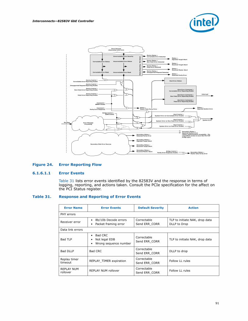
91
Interconnects—82583V GbE Controller
Figure 24. Error Reporting Flow
6.1.6.1.1 Error Events
Table 31 lists error events identified by the 82583V and the response in terms of logging, reporting, and actions taken. Consult the PCIe specification for the affect on the PCI Status register.
Table 31. Response and Reporting of Error Events
Command :: SERR# Enable
Command :: Parity Error Response
Status :: Signaled Target Abort
Status :: Received Target Abort
Status :: Received Master Abort
Status :: Detected Parity Error
Device Control :: Correctable Error Reporting Enable
Device Control :: Non-Fatal Error Reporting Enable
Device Control :: Fatal Error Reporting Enable
Device Control :: Unsupported Request Reporting Enable
Device Status :: Correctable Error Detected
Device Status :: Non-Fatal Error Detected
Device Status :: Fatal Error Detected
Device Status :: Unsupported Request Detected
Uncorrectable Error Severity
Uncorrectable Error Mask Correctable Error Mask
Uncorrectable Error StatusCorrectable Error Status
Sta
tus
Rep
orti
ng
-N
ot
Gat
ed
Secondary Status :: Detected Parity Error
Secondary Status :: Signaled Target Abort
Secondary Status :: Received System Error (Either implementation acceptable - the unqualified version is more like PCI P2P bridge spec)
Secondary Status :: Received Target Abort
Secondary Status :: Received Master Abort Secondary Status ::
Master Data Parity Error
Bridge Control :: SERR Enable
Bridge Control :: Parity Error Response Enable
Root Control :: System Error on Correctable Error Enable
Root Control :: System Error on Non-Fatal Error Enable
Root Control :: System Error on Fatal Error Enable
Root Error Command :: Correctable Error Reporting Enable
Root Error Command :: Non-Fatal Error Reporting Enable
Root Error Command :: Fatal Error Reporting Enable
Root Error Status
Rcv Msg
System Error
Interrupt
Status :: Signaled System Error
Secondary Side Error Sources
Error Sources(Associated with Port)
Error MessageProcessing
Status :: Master Data Parity Error
Error Name Error Events Default Severity Action
PHY errors
Receiver error• 8b/10b Decode errors• Packet framing error
CorrectableSend ERR_CORR
TLP to initiate NAK, drop dataDLLP to Drop
Data link errors
Bad TLP • Bad CRC• Not legal EDB• Wrong sequence number
CorrectableSend ERR_CORR
TLP to initiate NAK, drop data
Bad DLLP Bad CRCCorrectableSend ERR_CORR
DLLP to drop
Replay timer timeout REPLAY_TIMER expiration
CorrectableSend ERR_CORR
Follow LL rules
REPLAY NUM rollover REPLAY NUM rollover
CorrectableSend ERR_CORR
Follow LL rules
82583V GbE Controller—Interconnects
92
Data link layer protocol error
Violations of Flow Control initialization protocol
UncorrectableSend ERR_FATAL
TLP errors
Poisoned TLPreceived
TLP with Error ForwardingUncorrectableERR_NONFATALLog header
In case of poisoned completion, no more requests from this client.
UnsupportedRequest (UR)
• Wrong config access • MRdLk• Config Request Type1• Unsupported vendor
defined type 0 message• Not valid MSG code• Not supported TLP type• Wrong function number• Wrong TC/VC• Received target access
with data size > 64-bit• Received TLP outside
address range
UncorrectableERR_NONFATALLog header
Send completion with UR
Completion Timeout
Completion timeout timer expired
UncorrectableERR_NONFATAL
Send the read request again
Completer abortAttempts to write to the Flash device when writes are disabled (FWE=10b)
UncorrectableERR_NONFATALLog header
Send completion with CA
Unexpected completion
Received completion without a request for it (tag, ID, etc.)
UncorrectableERR_NONFATALLog header
Discard TLP
Receiver Overflow
Received TLP beyond allocated credits
UncorrectableERR_FATAL
Receiver behavior is undefined
Flow control protocol error
• Minimum Initial Flow Control Advertisements
• Flow control update for Infinite Credit advertisement
UncorrectableERR_FATAL
Receiver behavior is undefined
Malformed TLP (MP)
• Data payload exceed Max_Payload_Size
• Received TLP data size does not match length field
• TD field value does not correspond with the observed size
• Byte enables violations.• PM messages that don’t
use TC0.• Usage of unsupported VC
UncorrectableERR_FATALLog header
Drop the packet, free FC credits
Completion with unsuccessful completion status
No action (already done by originator of completion)
Free FC credits
Error Name Error Events Default Severity Action
93
Interconnects—82583V GbE Controller
6.1.6.1.2 Error Pollution
Error pollution can occur if error conditions for a given transaction are not isolated to the error's first occurrence. If the PHY detects and reports a receiver error, to avoid having this error propagate and cause subsequent errors at upper layers, the same packet is not signaled at the data link or transaction layers.
Similarly, when the data link layer detects an error, subsequent errors that occur for the same packet is not signaled at the transaction layer.
6.1.6.1.3 Completion With Unsuccessful Completion Status
A completion with unsuccessful completion status is dropped and not delivered to its destination. The request that corresponds to the unsuccessful completion is retried by sending a new request for the undeliverable data.
6.1.7 Link Layer
6.1.7.1 ACK/NAK Scheme
The 82583V supports two alternative schemes for ACK/NAK rate:1. ACK/NAK is scheduled for transmission following any TLP.2. ACK/NAK is scheduled for transmission according to timeouts specified in the PCIe
specification.
The PCIe Error Recovery bit, loaded from NVM, determines which of the two schemes is used.
6.1.7.2 Supported DLLPs
The following DLLPs are supported by the 82583V as a receiver:
Table 32. DLLPs Received by The 82583V
The following DLLPs are supported by the 82583V as a transmitter:
Remarks Remarks
ACK
NAK
PM_Request_Ack
InitFC1-P v2v1v0 = 000
InitFC1-NP v2v1v0 = 000
InitFC1-Cpl v2v1v0 = 000
InitFC2-P v2v1v0 = 000
InitFC2-NP v2v1v0 = 000
InitFC2-Cpl v2v1v0 = 000
UpdateFC-P v2v1v0 = 000
UpdateFC-NP v2v1v0 = 000
UpdateFC-Cpl v2v1v0 = 000

82583V GbE Controller—Interconnects
94
Table 33. DLLPs initiated by The 82583V
6.1.7.3 Transmit EDB Nullifying
In case of a retrain necessity, there is a need to guarantee that no abrupt termination of the Tx packet happens. For this reason, early termination of the transmitted packet is possible. This is done by appending the EDB to the packet.
6.1.8 PHY
6.1.8.1 Link Width
The 82583V supports a link width of x1 only.
6.1.8.2 Polarity Inversion
If polarity inversion is detected, the receiver must invert the received data.
During the training sequence, the receiver looks at Symbols 6-15 of TS1 and TS2 as the indicator of lane polarity inversion (D+ and D- are swapped). If lane polarity inversion occurs, the TS1 Symbols 6-15 received are D21.5 as opposed to the expected D10.2. Similarly, if lane polarity inversion occurs, Symbols 6-15 of the TS2 ordered set are D26.5 as opposed to the expected 5D5.2. This provides the clear indication of lane polarity inversion.
6.1.8.3 L0s Exit Latency
The number of FTS sequences (N_FTS), sent during L1 exit, is loaded from the NVM into an 8-bit read-only register.
Remarks1
1. UpdateFC-Cpl is not sent because of the infinite FC-Cpl allocation.
Remarks
ACK
NAK
PM_Enter_L1
PM_Enter_L23
PM_Active_State_Request_L1
InitFC1-P v2v1v0 = 000
InitFC1-NP v2v1v0 = 000
InitFC1-Cpl v2v1v0 = 000
InitFC2-P v2v1v0 = 000
InitFC2-NP v2v1v0 = 000
InitFC2-Cpl v2v1v0 = 000
UpdateFC-P v2v1v0 = 000
UpdateFC-NP v2v1v0 = 000

95
Interconnects—82583V GbE Controller
6.1.8.4 Reset
The PCIe PHY can initiate core reset to the 82583V. The reset can be caused by three sources:
• Upstream move to hot reset - Inband Mechanism (LTSSM).• Recovery failure (LTSSM returns to detect).• Upstream component move to disable.
6.1.8.5 Scrambler Disable
The Scrambler/de-scrambler functionality in the 82583V can be eliminated by two mechanisms:
• Upstream according to the PCIe specification.• NVM bit.
6.1.9 Performance Monitoring
The 82583V incorporates PCIe performance monitoring counters to provide common capabilities to evaluate performance. The 82583V implements four 32-bit counters to correlate between concurrent measurements of events as well as the sample delay and interval timers. The four 32-bit counters can also operate in a two 64-bit mode to count long intervals or payloads.
The list of events supported by the 82583V and the counters control bits are described in the memory register map.
6.2 Ethernet InterfaceThe 82583V MAC provides a complete CSMA/CD function, supporting IEEE 802.3 (10 Mb/s), 802.3u (100 Mb/s), 802.3z, and 802.3ab (1000 Mb/s) implementations. The 82583V performs all of the functions required for transmission, reception, and collision handling called out in the standards.
The GMII/MII mode used to communicate between the MAC and the PHY supports 10/100/1000 Mb/s operation, with both half- and full-duplex operation at 10/100 Mb/s, and only full-duplex operation at 1000 Mb/s.
Note: The 82583V MAC is optimized for full-duplex operation in 1000 Mb/s mode. Half-duplex 1000 Mb/s operation is not supported.
The PHY features 10/100/1000-BaseT signaling and is capable of performing intelligent power-management based on both the system power-state and LAN energy-detection (detection of unplugged cables). Power management includes the ability to shutdown to an extremely low (powered-down) state when not needed as well as ability to auto-negotiate to a lower-speed 10/100 Mb/s operation when the system is in low power-states.
6.2.1 MAC/PHY GMII/MII Interface
The 82583V MAC and PHY communicate through an internal GMII/MII interface that can be configured for either 1000 Mb/s operation (GMII) or 10/100 Mb/s (MII) mode of operation. For proper network operation, both the MAC and PHY must be properly configured (either explicitly via software or via hardware auto-negotiation) to identical speed and duplex settings. All MAC configuration is performed using device control registers mapped into system memory or I/O space; an internal MDIO/MDC interface, accessible via software, is used to configure the PHY operation.

82583V GbE Controller—Interconnects
96
The internal Gigabit Media Independent Interface (GMII) mode of operation is similar to MII mode of operation. GMII mode uses the same MDIO/MDC management interface and registers for PHY configuration as MII mode. These common elements of operation enable the 82583V MAC and PHY to cooperatively determine a link partner's operational capability and configure the hardware based on those capabilities.
6.2.1.1 MDIO/MDC
The 82583V implements an internal IEEE 802.3 MII Management Interface (also known as the Management Data Input/Output or MDIO Interface) between the MAC and PHY. This interface provides the MAC and software the ability to monitor and control the state of the PHY. The internal MDIO interface defines a physical connection, a special protocol that runs across the connection, and an internal set of addressable registers. The internal interface consists of a data line (MDIO) and clock line (MDC), which are accessible by software via the MAC register space.
Software can use MDIO accesses to read or write registers in either GMII or MII mode by accessing the 82583V's MDIC register (see section 9.2.2.7).
6.2.1.2 Other MAC/PHY Control and Status
In addition to the internal GMII/MII communication and MDIO interface between the MAC and the PHY, the 82583V implements a handful of additional internal signals between MAC and PHY, which provide richer control and features.
• PHY reset - The MAC provides an internal reset to the PHY. This signal combines the PCI_RST_N input from the PCI bus and the PHY Reset bit of the Device Control register (CTRL.PHY_RST).
• PHY link status indication - The PHY provides a direct internal indication of link status (LINK) to the MAC to indicate whether it has sensed a valid link partner. Unless the PHY has been configured via its MII management registers to assert this indication unconditionally, this signal is a valid indication of whether a link is present. The MAC relies on this internal indication to reflect the STATUS.LU status as well as to initiate actions such as generating interrupts on link status changes, re-initiating link speed sense, etc.
• PHY duplex indication - The PHY provides a direct internal indication to the MAC of its resolved duplex mode (FDX). Normally, auto-negotiation by the PHY enables the PHY to resolve full/duplex communications with the link partner (except when the PHY is forced through MII register settings). The MAC normally uses this signal after a link loss/restore to ensure that the MAC is configured consistently with the re-linked PHY settings. This indication is effectively visible through the MAC register bit STATUS.FD, each time MAC speed has not been forced.
• PHY speed indication(s) - The PHY provides direct internal indications (SPD_IND) to the MAC of its negotiated speed (10/100/1000 Mb/s). The result of this indication is effectively visible through the MAC register bits STATUS.SPEED each time MAC speed has not been forced.
• MAC Dx power state indication - The MAC indicates its ACPI power state (PWR_STATE) to the PHY to enable it to perform intelligent power-management (provided that the PHY power-management is enabled in the MAC CTRL register).
6.2.2 Duplex Operation for Copper PHY/GMII/MII Operation
The 82583V supports half-duplex and full-duplex 10/100 Mb/s MII mode or 1000 Mb/s GMII mode.
Configuring the duplex operation of the 82583V can either be forced or determined via the auto-negotiation process. See section 6.2.3 for details on link configuration setup and resolution.

97
Interconnects—82583V GbE Controller
6.2.2.1 Full Duplex
All aspects of the IEEE 802.3, 802.3u, 802.3z, and 802.3ab specifications are supported in full duplex operation. Full duplex operation is enabled by several mechanisms, depending on the speed configuration of the 82583V and the specific capabilities of the link partner used in the application. During full duplex operation, the 82583V might transmit and receive packets simultaneously across the link interface.
In full-duplex GMII/MII mode, transmission and reception are delineated independently by the GMII/MII control signals. Transmission starts at the assertion of TX_EN, which indicates there is valid data on the TX_DATA bus driven from the MAC to the PHY. Reception is signaled by the PHY by the assertion of the RX_DV signal, which indicates valid receive data on the RX_DATA lines to the MAC.
6.2.2.2 Half Duplex
The 82583V MAC can operate in half duplex.
In half duplex operation, the MAC attempts to avoid contention with other traffic on the link by monitoring the CRS signal provided by the PHY and deferring to passing traffic. When the CRS signal is de-asserted or after a sufficient Inter-Packet Gap (IPG) has elapsed after a transmission, frame transmission begins. The MAC signals the PHY with TX_EN at the start of transmission.
If a collision occurs, the PHY detects the collision and asserts the COL signal to the MAC. Transmitting the frame stops within four link clock times and the 82583V sends a JAM sequence onto the link. After the end of a collided transmission, the 82583V backs off and attempts to re-transmit per the standard CSMA/CD method.
Note: The re-transmissions are done from the data stored internally in the 82583V MAC transmit packet buffer (no re-access to the data in host memory is performed).
After a successful transmission, the 82583V is ready to transmit any other frame(s) queued in the MAC's transmit FIFO, after the minimum Inter-Frame Spacing (IFS) of the link has elapsed.
During transmit, the PHY is expected to signal a carrier-sense (assert the CRS signal) back to the MAC before one slot time has elapsed. The transmission completes successfully even if the PHY fails to indicate CRS within the slot time window; if this situation occurs, the PHY can either be configured incorrectly or be in a link down situation. Such an event is counted in the Transmit Without CRS statistic register (see section 9.2.7.11).
6.2.3 Auto-Negotiation & Link Setup Features
The method for configuring the link between two link partners is highly dependent on the mode of operation.
Configuration of the link can be accomplished by several methods ranging from:• software's forcing link settings • software-controlled negotiation • MAC-controlled auto-negotiation • auto-negotiation initiated by a PHY.
The following sections describe processes of bringing the link up including configuration of the 82583V and the transceiver, as well as the various methods of determining duplex and speed configuration.

82583V GbE Controller—Interconnects
98
The PHY performs auto-negotiation per 802.3ab clause 40 and extensions to clause 28. Link resolution is obtained by the MAC from the PHY after the link has been established. The MAC accomplishes this via the MDIO interface, via specific signals from the PHY to the MAC, or by MAC auto-detection functions.
6.2.3.1 Link Configuration
Link configuration is generally determined by PHY auto-negotiation. The software device driver must intervene in cases where a successful link is not negotiated or a user desires to manually configure the link. The following sections discuss the methods of link configuration for copper PHY operation.
6.2.3.1.1 PHY Auto-Negotiation (Speed, Duplex, Flow-Control)
The PHY performs the auto-negotiation function. The details of this operation are described in the IEEE P802.3ab draft standard and are not included here.
Auto-negotiation provides a method for two link partners to exchange information in a systematic manner in order to establish a link configuration providing the highest common level of functionality supported by both partners. Once configured, the link partners exchange configuration information to resolve link settings such as:
• Speed: 10/100/1000 Mb/s• Duplex: full or half• Flow control operation
PHY specific information required for establishing the link is also exchanged.
Note: If flow control is enabled in the 82583V, the settings for the desired flow control behavior must be set by software in the PHY registers and auto-negotiation restarted. After auto-negotiation completes, the software device driver must read the PHY registers to determine the resolved flow control behavior of the link and reflect these in the MAC register settings (CTRL.TFCE and CTRL.RFCE). If no software device driver is loaded and auto-negotiation is enabled, then hardware sets these bits in accordance with the auto-negotiation results.
Note: By default, the PHY advertises flow control support.
Note: Once PHY auto-negotiation completes, the PHY asserts a link indication (LINK) to the MAC. Software must set the Set Link Up bit in the Device Control register (CTRL.SLU) before the MAC recognizes the link indication from the PHY and can consider the link to be up.

99
Interconnects—82583V GbE Controller
6.2.3.1.2 MAC Speed Resolution
For proper link operation, both the MAC and PHY must be configured for the same speed of link operation. The speed of the link can be determined and set by several methods with the 82583V. These include:
• Software-forced configuration of the MAC speed setting based on PHY indications, which can be determined as follows:— Software reads of PHY registers directly to determine the PHY's auto-negotiated
speed— Software reads the PHY's internal PHY-to-MAC speed indication (SPD_IND)
using the MAC STATUS.SPEED register— Software signals the MAC to attempt to auto-detect the PHY speed from the
PHY-to-MAC RX_CLK, then programs the MAC speed accordingly• The MAC automatically detecting and setting the link speed of the MAC based on
PHY indications by:— Using the PHY's internal PHY-to-MAC speed indication (SPD_IND), setting the
MAC speed automatically— Attempting to auto-detect the PHY speed from the PHY-to-MAC RX_CLK and
setting the MAC speed automatically
Aspects of these methods are discussed in the sections that follow.
6.2.3.1.2.1 Forcing MAC Speed
There might be circumstances when the software device driver must forcibly set the link speed of the MAC. This can occur when the link is manually configured. To force the MAC speed, the software device driver must set the CTRL.FRCSPD (force-speed) bit to 1b and then write the speed bits in the Device Control register (CTRL.SPEED) to the desired speed setting. See section 9.2.2.1 for details.
Note: Forcing the MAC speed using CTRL.FRCSPD overrides all other mechanisms for configuring the MAC speed and can yield non-functional links if the MAC and PHY are not operating at the same speed/configuration.
When forcing the 82583V to a specific speed configuration, the software device driver must also ensure the PHY is configured to a speed setting consistent with MAC speed settings. This implies that software must access the PHY registers to either force the PHY speed or to read the PHY status register bits that indicate link speed of the PHY.
Note: Forcing speed settings by CTRL.SPEED can also be accomplished by setting the CTRL_EXT.SPD_BYPS bit. This bit bypasses the MAC's internal clock switching logic and enables the software device driver complete control of when the speed setting takes place. The CTRL.FRCSPD bit uses the MAC's internal clock switching logic, which does delay the affect of the speed change.
6.2.3.1.2.2 Using PHY Direct Link-Speed Indication
The 82583V PHY provides a direct internal indication of its speed to the MAC (SPD_IND). The most direct method for determining the PHY link speed and either manually or automatically configuring the MAC speed is based on these direct speed indications.
For MAC speed to be set/determined from these direct internal indications from the PHY, the MAC must be configured such that CTRL.ASDE and CTRL.FRCSPD are both 0b (both auto-speed detection and forced-speed override are disabled). As a result, the MAC speed is reconfigured automatically each time the PHY indicates a new link-up event to the MAC.

82583V GbE Controller—Interconnects
100
When MAC speed is neither forced nor auto-sensed by the MAC, the current MAC speed setting and the speed indicated by the PHY is reflected in the Device Status register bits STATUS.SPEED.
6.2.3.1.3 MAC Full/Half Duplex Resolution
The duplex configuration of the link is also resolved by the PHY during the auto-negotiation process. The 82583V PHY provides an internal indication to the MAC of the resolved duplex configuration using an internal full-duplex indication (FDX).
This internal duplex indication is normally sampled by the MAC each time the PHY indicates the establishment of a good link (LINK indication). The PHY's indicated duplex configuration is applied in the MAC and reflected in the MAC Device Status register (STATUS.FD).
Software can override the duplex setting of the MAC via the CTRL.FD bit when the CTRL.FRCDPLX (force duplex) bit is set. If CTRL.FRCDPLX is 0b, the CTRL.FD bit is ignored and the PHY's internal duplex indication applied.
6.2.3.1.4 Using PHY Registers
The software device driver might be required under some circumstances to read from or write to the MII management registers in the PHY. These accesses are performed via the MDIC registers (see section 9.2.2.7). The MII registers enable the software device driver to have direct control over the PHY's operation, which might include:
• Resetting the PHY• Setting preferred link configuration for advertisement during the auto-negotiation
process• Restarting the auto-negotiation process• Reading auto-negotiation status from the PHY• Forcing the PHY to a specific link configuration
The set of PHY management registers required for all PHY devices can be found in the IEEE P802.3ab draft standard. The registers for the 82583V PHY are described in section 9.2.
6.2.3.1.5 Comments Regarding Forcing Link
Forcing link requires the software device driver to configure both the MAC and PHY in a consistent manner with respect to each other. After initialization, the software device driver configures the desired modes in the MAC, then accesses the PHY registers to set the PHY to the same configuration.
Before enabling the link, the speed and duplex settings of the MAC can be forced by software using the CTRL.FRCSPD, CTRL.FRCDPX, CTRL.SPEED, and CTRL.FD bits. After the PHY and MAC have both been configured, the software device driver should write a 1b to the CTRL.SLU bit.
6.2.4 Loss of Signal/Link Status Indication
PHY LOS/LINK signal provides an indication of physical link status to the MAC. This signal from the PHY indicates whether the link is up or down; typically indicated after successful auto-negotiation. Assuming that the MAC is configured with CTRL.SLU = 1b, the MAC status bit STATUS.LU when read, generally reflects whether the PHY has link (except under forced-link setup where even the PHY link indication might have been forced).
101
Interconnects—82583V GbE Controller
When the link indication from the PHY is de-asserted, the MAC considers this to be a transition to a link-down situation (such as, cable unplugged, loss of link partner, etc.). If the LSC (Link Status Change) interrupt is enabled, the MAC generates an interrupt to be serviced by the software device driver. See section 7.4 and section 9.2.4 for more details.
6.2.5 10/100 Mb/s Specific Performance Enhancements
6.2.5.1 Adaptive IFS
The 82583V supports back-to-back transmit Inter-Frame-Spacing (IFS) of 960 ns in 100 Mb/s operation and 9.6 μs in 10 Mb/s operation. Although back-to-back transmission is normally desirable, sometimes it can actually hurt performance in half-duplex environments due to excessive collisions. Excessive collisions are likely to occur in environments where one station is attempting to send large frames back-to-back, while another station is attempting to send acknowledge (ACK) packets.
The 82583V contains an Adaptive IFS register (see section 9.2.6.3) that enables the implementation of a driver-based adaptive IFS algorithm for collision reduction, which is similar to Intel's other Ethernet products (such as PRO/100 adapters). Adaptive IFS throttles back-to-back transmissions in the transmit MAC and delays their transfer to the CSMA/CD transmit function and then can be used to delay the transmission of back-to-back packets on the wire. Normally, this register should be set to zero. However, if additional delay is desired between back-to-back transmits, then this register can be set with a value greater than zero. This can be helpful in high-collision half-duplex environments.
The AIFS field provides a similar function to the IGPT field in the TIPG register (see section 9.2.6.3). However, this Adaptive IFS throttle register counts in units of GTX/MTX_CLK clocks, which are 800 ns, 80 ns, 8 ns for 10/100/1000 Mb/s mode respectively, and is 16 bits wide, thus providing a greater maximum delay value.
Using values lower than a certain minimum (determined by the ratio of GTX/MTX_CLK clock to link speed), has no effect on back-to-back transmission. This is because the 82583V does not start transmission until the minimum IEEE IFS (9.6 μs at 10 Mb/s, 960 ns at 100 Mb/s, and 96 ns at 1000 Mb/s) has been met regardless of the value of Adaptive IFS. For example, if the 82583V is configured for 100 Mb/s operation, the minimum IEEE IFS at 100 Mb/s is 960 ns. Setting AIFS to a value of 10 (decimal) would not effect back-to-back transmission time on the wire because the 800 ns delay introduced (10 * 80 ns = 800 ns) is less than the minimum IEEE IFS delay of 960 ns. However, setting this register with a value of 20 (decimal), which corresponds to 1600 ns for the above example, would delay back-to-back transmits because the ensuing 1600 ns delay is greater than the minimum IFS time of 960 ns.
It is important to note that this register has no effect on transmissions that occur immediately after receives or on transmissions that are not back-to-back (unlike the IPGR1 and IPGR2 values in the TIPG register (see section 9.2.6.2). In addition, Adaptive IFS also has no effect on re-transmission timing (re-transmissions occur after collisions). Therefore, AIFS is only enabled in back-to-back transmission.
Note: The AIFS value is not additive to the TIPG.IPGT value; instead, the actual IPG equals the larger of the two, AIFS and TIPG.IPGT.

82583V GbE Controller—Interconnects
102
6.2.6 Flow Control
Flow control as defined in 802.3x, as well as the specific operation of asymmetrical flow control defined by 802.3z, are supported in the MAC. The following seven registers are defined for the implementation of flow control:
• Flow Control Address Low (FCAL) - 6-byte flow control multicast address• Flow Control Address High (FCAH) - 6-byte flow control multicast address• Flow Control Type (FCT) - 16-bit field that indicates flow control type• Flow Control Receive Thresh Hi (FCRTH) - 13-bit high-water mark indicating receive
buffer fullness• Flow Control Receive Thresh Lo (FCRTL) - 13-bit low-water mark indicating receive
buffer emptiness• Flow Control Transmit Timer Value (FCTTV) - 16-bit timer value to include in
transmitted pause frames• Flow Control Refresh Threshold Value (FCRTV) - 16-bit pause refresh threshold
value
Flow control allows for local controlling of network congestion levels. Flow control is implemented as a means of reducing the possibility of receive buffer overflows. Receive buffer overflows result in the dropping of received packets. Flow control is accomplished by notifying the transmitting station that the receiving station receive buffer is nearly full.
Implementing asymmetric flow control allows for one link partner to send flow control packets while being allowed to ignore their reception. For example, not required to respond to pause frames.
6.2.6.1 MAC Control Frames and Reception of Flow Control Packets
Three comparisons are used to determine the validity of a flow control frame. All three must be true for a positive result.1. A match on the six-byte multicast address for MAC control frames or to the station
address of the device (Receive Address Register 0).2. A match on the Type field.3. A comparison of the MAC Control Opcode field.
The 802.3x standard defines the MAC control frame multicast address as 01-80-C2-00-00-01. This address must be loaded into the Flow Control Address Low/High registers (FCAL/FCAH).
The Flow Control Type (FCT) register contains a 16-bit field that is compared against the flow control packet's Type field to determine if it is a valid flow control packet: XON or XOFF. 802.3x reserves this as 0x8808. This value must be loaded into the Flow Control Type register.
The final check for a valid pause frame is the MAC control opcode. At this time, only the pause control frame opcode is defined. It has a value of 0x0001.
Frame-based flow control differentiates XOFF from XON based on the value of the Pause Timer field. Non-zero values constitute XOFF frames while a value of zero constitutes an XON frame. Values in the timer field are in units of slot time. A slot time is hard wired to 64-byte times or 512 ns.
Note: An XON frame signals the cancellation of the pause from being initiated by an XOFF frame (pause for zero slot times).

103
Interconnects—82583V GbE Controller
Figure 25. 802.3x MAC Control Frame Format
Where S is the start-of-packet delimiter and T is the first part of the end-of-packet delimiters for 802.3z encapsulation.
The receiver is enabled to receive flow control frames if flow control is enabled via the RFCE bit in the Device Control (CTRL) register.
Note: Flow control capability must be negotiated between link partners via the auto-negotiation process. The auto-negotiation process might modify the value of these bits based on the resolved capability between the local device and the link partner.
Once the receiver validates receiving an XOFF or pause frame, the 82583V performs the following:
• Increments the appropriate statistics register(s).• Sets the TXOFF bit in the Device Status (STATUS) register.• Initializes the pause timer based on the packet's Pause Timer field.• Disables packet transmission or schedules the disabling of transmissions after the
current packet completes.
Resuming transmission can occur under the following conditions:• An expired pause timer• Receiving an XON frame (a frame with its pause timer set to zero)
Either condition clears the TXOFF status bit in the Device Status register and transmission can resume. Note that hardware records the number of received XON frames.
(min_FrameSize -160)/8Bytes
Preamble...
SFD
S
FCS
T
Up to 6 Bytes
1 Byte
1 Byte
DestinationAddress
6 Bytes
SourceAddress
6 Bytes
Type/Length2 Bytes
MAC ControlOpcode
2 Bytes
MAC ControlParameters
1 Byte
4 Bytes

82583V GbE Controller—Interconnects
104
6.2.6.2 Discard Pause Frames and Pass MAC Control Frames
Two bits in the Receive Control register are implemented specifically for control over receipt of pause and MAC control frames. These bits are Discard PAUSE Frames (DPF) and Pass MAC Control Frames (PMCF). See section 9.2.6.2 for DPF and PMCF bit definitions.
The DPF bit forces the discarding of any valid pause frame addressed to the 82583V's station address. If the packet is a valid pause frame and is addressed to the station address (receive address [0]), the 82583V does not pass the packet to host memory if the DPF bit is set to logic high. However, if a flow control packet is sent to the station address and is a valid flow control frame, it is then be transferred when DPF is set to 0b. This bit has no affect on pause operation, only the DMA function.
The PMCF bit enables for the passing of any valid MAC control frames to the system, which does not have a valid pause opcode. In other words, the frame must have the correct MAC control frame multicast address (or the MAC station address) as well as the correct Type field match with the FCT register, but does not have the defined pause opcode of 0x0001. Frames of this type are transferred to host memory when PMCF is a logic high.
6.2.6.3 Transmitting PAUSE Frames
Transmitting pause frames is enabled by software by writing a 1b to the TFCE bit in the Device Control register.
Note: Similar to receiving flow control packets, XOFF packets can be transmitted only if this configuration has been negotiated between the link partners via the auto-negotiation process. In other words, setting this bit indicates the desired configuration. Resolving the auto-negotiation process is described in section 6.2.3.
The content of the Flow Control Receive Threshold High register determines at what point hardware transmits a pause frame. Hardware monitors the fullness of the receive FIFO and compares it with the contents of FCRTH. When the threshold is reached, hardware sends a pause frame with its pause time field equal to FCTTV.
At the time threshold is reached, the hardware starts counting an internal shadow counter FCRTV (reflecting the pause time-out counter at the partner end) from zero. When the counter reaches the value indicated in the FCRTV register, then, if the pause condition is still valid (meaning that the buffer fullness is still above the low watermark), an XOFF message is sent again and the shadow counter starts counting again.
Once the receive buffer fullness reaches the low water mark, hardware sends an XON message (a pause frame with a timer value of zero). Software enables this capability with the XONE field of the FCRTL.
Hardware sends one more pause frame if it has previously sent one and the FIFO overflows (so the threshold must not be set greater than the FIFO size). This is intended to minimize the amount of packets dropped if the first pause frame does not reach its target. Since the secure receive packets use the same data path, the behavior is identical when secure packets are received.
Note: Transmitting flow control frames should only be enabled in full-duplex mode per the IEEE 802.3 standard. Software should ensure that transmitting flow control packets is disabled when the 82583V is operating in half-duplex mode.
Note: Regardless of the mechanism above, each time a receive packet is dropped due to lack of space in the internal receive buffer, a pause frame is transmitted as well (if TFCE bit in the Device Control register is enabled).

105
Interconnects—82583V GbE Controller
6.2.6.4 Software Initiated Pause Frame Transmission
The 82583V has the added capability to transmit an XOFF frame via software. This is accomplished by software writing a 1b to the SWXOFF bit of the Transmit Control register. Once this bit is set, hardware initiates transmitting a pause frame in a manner similar to that automatically generated by hardware.
The SWXOFF bit is self-clearing after the pause frame has been transmitted.
The state of the CTRL.TFCE bit or the negotiated flow control configuration does not affect software generated pause frame transmission.
Note: Software sends an XON frame by programming a zero in the Pause Timer field of the FCTTV register.
Note: XOFF transmission is not supported in 802.3x for half-duplex links. Software should not initiate an XOFF or XON transmission if the 82583V is configured for half-duplex operation.
6.3 SPI Non-Volatile Memory Interface
6.3.1 General Overview
The 82583V requires non-volatile content for the 82583V configuration. The Non-Volatile Memory (NVM) might contain the following main regions:
• LAN configuration space accessed by hardware - loaded by the 82583V after power up, PCI reset de-assertion, D3->D0 transition, or a software commanded EEPROM read (CTRL_EXT.EE_RST).
• LAN configuration space accessed by software - used by software only. The meaning of these registers as listed here as a convention for the software only and is ignored by the 82583V.
6.3.2 Supported NVM Devices
Some Intel LAN controllers require both an EEPROM and Flash device for storing LAN data. However, the 82583 reduces the Bill of Material (BOM) cost by consolidating the EEPROM and Flash into a single non-volatile memory device. The NVM is connected to a single Serial Peripheral Interface (SPI).
The 82583 is compatible with many sizes of 4-wire SPI NVM devices. The required NVM size is dependent upon system requirements.

82583V GbE Controller—Interconnects
106
6.3.3 NVM Device Detection
The 82583V detects the device connected on the SPI interface in two phases. 1. It first detects the device type by the state of the NVMT strapping pin. 2. It then looks at the NVM content depending on a valid signature in word 0x12 in the
NVM.
In reference to the EEPROM, the 82583V detects the length of the address bytes by sensing the signature at word 0x12. It then sets the NVADDS field in the EEC register. The exact size of the NVM is fetched by the 82583V from word 0x0F and is stored in the NVSize field in the EEC register. When operating with an EEPROM that has an invalid signature, software can force the address length via the NVADDS field in the EEC register. Controlling the address length enables software to access the EEPROM via the parallel EERD and EEWR registers in all cases including invalid signature.
6.3.3.1 CRC Field
CRC calculation is done by software.
Table 34. NVM Configuration Size
Configuration Minimum NVM Size Memory Family
No iSCSI boot1 1 Kb SPI EEPROM
PXE only 512 Kb SPI Flash
iSCSI boot only 2 Mb SPI Flash
Both iSCSI boot and PXE 4 Mb SPI Flash
Table 35. Compatible EEPROM Parts
Vendor 1 Kb 2 Kb 32 Kb
Atmel* AT25010N AT25020N AT25010N-10SI-2.7
STM* 95010W6 95020W6 AT25320N
Catalyst* CAT25010S CAT25020S CAT25C320S
Table 36. Compatible Flash Parts
Vendor 512 Kb 1 Mb 2 Mb 4 Mb 8 Mb
Winbond* N/A W25X10BV W25X20BV W25X40BV N/A
Atmel AT25F512B N/A AT25DF021 AT25DF041A AT25DF081A
PMC* 25LV512A 25LV010A 25LV020 N/A N/A
SST* SST25VF512 SST25VF010A SST25VF020B SST25VF040B SST25VF080B

107
Interconnects—82583V GbE Controller
6.3.4 Device Operation with an External EEPROM
When the 82583V is connected to an external EEPROM, it provides similar functionality to its predecessors with the following enhancements:
• Enables a complete parallel interface for read/write to the EEPROM.• Enables software to specify explicitly the address length, thus eliminating the need
for bit banging access even on an empty EEPROM.
6.3.5 Device Operation with Flash
As previously stated, the 82583V merges the legacy EEPROM and Flash content in a single Flash device. The 82583V copies the lower section in the Flash device to an internal shadow RAM. The interface to the shadow RAM is the same as the interface for an external EEPROM device. This mechanism provides a seamless backward compatible interface for software to the legacy EEPROM space as if an external EEPROM device is connected.
The 82583V supports Flash devices with a block erase size of 4 KB. Note that many Flash vendors are using the term sector differently. This document uses the term Flash sector for a logic section of 4 KB.
6.3.5.1 LAN Configuration Sectors
Flash devices require a block erase instruction in case a cell is modified from 0b to 1b. As a result, in order to update a single byte (or block of data) it is required to erase it first. The first addresses of the Flash contain the device configuration and must always be valid. The 82583V maintains two sectors of 4 KB: S0 and S1 for the configuration content. At least one of these two sectors is valid at any given time or else the 82583V is set by the hardware default. section 6.3.6 provides more details on the shadow RAM and the first two sectors.
6.3.6 Shadow RAM
The 82583V includes an internal 4 KB shadow RAM of the first 4 KB Flash sector(s). When the 82583V is connected to a Flash device the legacy configuration parameters might reside in any of the first two 4 KB sectors (S0 or S1) in the Flash. The 82583V copies that data to an internal shadow memory. The shadow RAM emulates a seamless EEPROM interface to the rest of the 82583V and host CPU. This way the legacy configuration content is accessible to software and firmware on the same EEPROM registers as on previous GbE controllers.
Figure 26 shows the shadow RAM mapping and interface relative to the Flash and the EEPROM. The external EEPROM and the shadow RAM share the same interface. The 82583V might access the EEPROM or shadow RAM according to the setting of the SELSHAD bit in the EEC register. By hardware default, the SELSHAD bit is set by the NVMT strapping pin so that the EEPROM is selected in case of external EEPROM and the shadow RAM is selected in the case of external Flash.
Note: Access to the shadow RAM uses the same interface as the external EEPROM with the exception that bit banging is not supported for the shadow RAM.

82583V GbE Controller—Interconnects
108
Figure 26. NVM Shadow RAM
6.3.6.1 Flash Mode
The 82583V is initialized from the NVM. As part of the initialization sequence, the 82583V copies the 4 KB content of S0 or S1 from the Flash to the shadow RAM. Any access to the EEPROM interface is directed to the shadow RAM. Following any write access to the shadow RAM by software or firmware, the data should also be updated in the Flash. The 82583V maintains a watchdog timer defined by the FLASHT register to minimize Flash updates. The timer is triggered by any write access to the shadow RAM. The 82583V updates the Flash from the shadow RAM when the FLASHT timer expires or when firmware or software request explicitly to update the Flash by setting the FLUPD bit in the FLA register. The 82583V copies the content of the shadow RAM to the inactive configuration sector and then makes it the active one. The Flash update sequence is listed in the steps that follow:1. Initiates block erase instruction(s) to the inactive sector (the inactive sector is
defined by the inverse value of the SEC1VAL bit in the EEC register).2. Copy the shadow RAM to the inactive sector while the signature word is copied last.3. Clear the signature word in the active sector to make it invalid.4. Toggle the state of the SEC1VAL bit in the EEC register to indicate that the inactive
sector became the active one and visa versa.
Note: Software should be aware of the fact that actual programming to the Flash might require a long latency following the write access to the shadow RAM. Software might poll the FLUDONE bit in the FLCTL register to complete the Flash programming, when required.
6.3.6.2 EEPROM Mode
When the 82583V is attached to an external EEPROM, any access to the EEPROM interface is directed to the external EEPROM.
Shadow RAM
Address 00
Address 4K
Address 8K
EEPROM Interface
Sector 0
Sector 1
EEPROM …
EEC.SELSHAD
LAN Flash …
109
Interconnects—82583V GbE Controller
6.3.7 NVM Clients and Interfaces
There are several clients that might access the NVM or shadow RAM listed in the following table. Listed are the various clients and their access type to the NVM: software device driver, BIOS, firmware and hardware.
Table 37. Clients and Access Type to the NVM
6.3.7.1 Memory Mapped Host Interface via LAN Flash BAR
Software might read and write to the Flash via the LAN Flash BAR. The Flash BAR is mapped to the physical Flash at offset 0x0. The 82583V supports read byte, word or Dword and write byte through this interface. The host CPU waits (stalled) until the read access to the Flash completes.
Note: One of the first two sectors of 4 KB in the Flash are also reflected in the shadow RAM. During normal operation, when software requires access to these sectors it should access the shadow RAM. Direct write accesses to the Flash in this space via the Flash BAR might cause non-coherency between the Flash and the shadow RAM.
Note: Flash BAR access while FLA.FL_REQ is asserted (and granted) is forbidden.
6.3.7.2 CSR Mapped Host Interface
Software has bit banging and parallel accesses to the NVM or shadow RAM via the registers in the CSR space. The 82583V supports the following cycles on the parallel interface: posted write, posted read, block erase and device erase. Access to the configuration space in the first two sectors is directed via the EEPROM registers regardless of the external physical device. Access to the rest of the NVM space is done according to the type of the physical device: Flash registers in reference to Flash and EEPROM registers in reference to EEPROM. EEPROM CSR registers are as follows:
• EEC register for bit banging and device control• EERD and EEWR registers for parallel read and write access
The Flash CSR registers are as follows:• FLA register and EEC register for bit banging and device control
Client + Interface NVM port NVM instructions
Host CPU on EEC CSR EEPROM Legacy bit banging
Host CPU on EERD and EEWR EEPROM Parallel word read and write to EEPROM or shadow RAM
(controlled by the EEC.SELSHAD bit)
EE CSR EEPROM Parallel word read and write to EEPROM or shadow RAM
Host CPU on FLA CSR Flash Legacy bit banging and Flash erase instructions
Host CPU via BAR Flash Read byte word and Dword and byte programming1
1. Following a write instruction or erase instructions to the Flash, the 82583V initiates seamless write enablebefore the write or erase instructions and polls the status at the end to check its completion.
Host CPU via FLSWxxx CSR registers Flash Host write access to the Flash no support for burst (multiple
byte) writes
Direct HW accesses Both Read EEPROM/shadow RAM at device initialization

82583V GbE Controller—Interconnects
110
Note: When software accesses the EEPROM or Flash spaces via the bit banging interface, it should follow these steps:1. Write a 1b to the Request bit in the FLA or EEC registers.2. Poll the Grant bit in the FLA or EEC registers until its ready.3. Access the NVM using the direct interface to its signaling via the EEC or FLA
registers.4. When access completes, software should clear the Request bit.
Note: Following a write or erase instruction, software should clear the Request bit only after it checked that the cycles were completed by the NVM.
6.3.7.3 CSR Mapped Firmware Interface
Firmware might access the NVM or shadow RAM via the NVM Control registers in the CSR space with the following capabilities:
• Word read and write accesses to the EEPROM or shadow RAM via the EECTL and EEDATA registers.
• Read and write DMA and block erase to the Flash interface via the FLCTL and FLDATA registers. Flash accesses are mapped to the physical NVM at offset 0x0. Note that nominal accesses to the first two 4 KB sectors should be addressed to the shadow RAM via the EEPROM interface.
6.3.8 NVM Write and Erase Sequence
6.3.8.1 Software Flow to the Bit Banging Interface
When software accesses the EEPROM or Flash CSR registers to the bit banging interface it should follow these steps:1. Write a 1b to the Request bit in the FLA or EEC registers.2. Poll the Grant bit in the FLA or EEC registers until its ready.3. Access the NVM using the direct interface to its signaling via the EEC or FLA
registers.4. When access is achieved, software should clear the Request bit. Note that following
a write or erase instruction, software should clear the Request bit only after it checked that the cycles were completed by the NVM.
6.3.8.2 Software Byte Program Flow to the EEPROM Interface
Software initiates a write cycle to the NVM on the parallel EEPROM as follows:1. Poll the Done bit in the EEWR register until its set.2. Write the data word, its address, and the Start bit to the EEWR register.
As a response, hardware executes the following steps:
Case 1 - The 82583V is connected to a physical EEPROM device:1. Initiate an autonomous write enable instruction.2. Initiate the program instruction right after the enable instruction.3. Poll the EEPROM status until programming completes.4. Set the Done bit in the EEWR register.

111
Interconnects—82583V GbE Controller
Case 2 - The 82583V is connected to a physical Flash device:1. The 82583V writes the data to the shadow RAM and sets the Done bit in the EEWR
register.2. Update of the shadow RAM to the Flash device as described in section 6.3.6.
6.3.8.3 Flash Byte Program Flow
Software initiates a byte write cycle via the Flash BAR as follows:1. Write access to the Flash must be first enabled in the FLEW field in the EEC register.2. Poll the FLBUSY flag in the FLA register until cleared.3. Write the data byte to the Flash through the Flash BAR.4. Repeat the steps 2 and 3 if multiple bytes should be programmed.5. Clear the write enable in the FLEW field in the EEC register to protect the Flash
device.
As a response, hardware executes the following steps for each write access:1. Initiate autonomous write enable instruction.2. Initiate the program instruction right after the enable instruction.3. Poll the Flash status until programming completes.4. Clear the FLBUSY bit in the FLA register.
Note: This section explains only the actual programming of a single byte or multiple bytes.
6.3.8.4 Flash Erase Flow
Device Erase Flow:
Erase instructions flow by software is almost identical to the program flow:1. Erase access to the Flash must be first enabled in the FLEW field in the EEC
register.2. Poll the FLBUSY flag in the FLA register until cleared.3. Set the Flash Erase bit (FL_ER) in the FLA register.4. Clear the Erase enable in the FLEW field in the EEC register to protect the Flash
device.
6.3.8.5 Flash Burst Program Flow
The 82583V provides a burst engine that can be useful for initial programming of the entire Flash image according to the following flow:1. Set the ADDR field with the byte resolution address in the FLSWCTL register.2. Set the CMD field to 01b, which is the DMA write setting in the FLSWCTL register.3. Write the first 32 bits of data to the FLSWGDATA register.4. Set the RDCNT field to the byte count number in the FLSWCNT register.5. Set the CMDV field in the FLSWCTL register to start a DMA write.6. Hardware starts accessing the SPI bus and begins writing the first 32 bits from the
FLSWDATA register.7. Once hardware writes the 32-bit data to the Flash, the DONE bit in the FLSWCTL
register is set indicating the next 32 bits are required.

82583V GbE Controller—Interconnects
112
8. Until new data is written to the FLSWDATA register, the Flash clock is paused.9. Once data is written to the FLSWDATA by the software, the DONE bit in the
FLSWCTL register is cleared and is set after hardware writes it to the Flash.10. After all bytes are written to the Flash, hardware completes the cycle on the SPI
bus and sets the WRDONE bit in the FLSWCTL register indicating that the entire burst has completed.
6.3.8.6 Flash Programming Flow of S0 and S1
Other than initial programming of the Flash device, software and firmware should not access the configuration sectors: S0 and S1. Any access to the configuration flow should go to the Shadow RAM via the EEPROM interface registers.

113
Interconnects—82583V GbE Controller
Note: This page intentionally left blank.

82583V GbE Controller—Inline Functions
114
7.0 Inline Functions
7.1 Packet ReceptionPacket reception consists of recognizing the presence of a packet on the wire, performing address filtering, storing the packet in the receive data FIFO, transferring the data to the receive queue in host memory, and updating the state of a receive descriptor.
7.1.1 Packet Address Filtering
Hardware stores incoming packets in host memory subject to the following filter modes. If there is insufficient space in the receive FIFO, hardware drops them and indicates the missed packet in the appropriate statistics registers.
The following filter modes are supported:
• Exact unicast/multicast— The destination address must exactly match one of 16 stored addresses. These
addresses can be unicast or multicast.
Note: The software device driver can only use 15 entries (entries 0-14).• Promiscuous unicast
— Receive all unicasts• Multicast
The upper bits of the incoming packet's destination address index is a bit vector that indicates whether to accept the packet; if the bit in the vector is one, accept the packet, otherwise, reject it. The 82583V provides a 4096-bit vector. Software provides four choices of which bits are used for indexing. These are [47:36], [46:35], [45:34], or [43:32] of the internally stored representation of the destination address (see Figure 43)
• Promiscuous multicast— Receive all multicast packets
• VLAN
Receive all VLAN packets that are for this station and have the appropriate bit set in the VLAN filter table. A detailed discussion and explanation of VLAN packet filtering is contained in section 7.5.3.
Normally, only good packets are received.

115
Inline Functions—82583V GbE Controller
Good packets are defined as those packets with no:
• CRC error• Symbol error• Sequence error• Length error• Alignment error• Where carrier extension or RX_ERR errors are detected.
However, if the Store-Bad-Packet bit is set in the Device Control register (RCTL.SBP), then bad packets that pass the filter function are stored in host memory. Packet errors are indicated by error bits in the receive descriptor (RDESC.ERRORS). It is possible to receive all packets, regardless of whether they are bad, by setting the promiscuous enables and the Store-Bad-Packet bit.
Note: CRC errors before the SFD are ignored. Every packet must have a valid SFD (RX_DV with no RX_ER in the GMII/MII interface) in order to be recognized by the device (even bad packets).
7.1.2 Receive Data Storage
Memory buffers pointed to by descriptors store packet data. Hardware supports the following receive buffer sizes:
• 256B 512B 1024B 2048B 4096B 8192B 16384B• FLXBUF x 1024B while FLXBUF=1,2,3,…15
Buffer size is selected by bit settings in the Receive Control register (RCTL.BSIZE, RCTL.BSEX, RCTL.DTYP and RCTL. FLXBUF).
The 82583V (in legacy mode) places no alignment restrictions on receive memory buffer addresses. This is desirable in situations where the receive buffer was allocated by higher layers in the networking software stack, as these higher layers might have no knowledge of a specific device's buffer alignment requirements.
Note: Although alignment is completely unrestricted, it is highly recommended that software allocate receive buffers on at least cache-line boundaries whenever possible.
Note: The larger buffer sizes are only offered to provide compatibility with other silicon types. Jumbo frames are not supported with the 82583V.
7.1.3 Legacy Receive Descriptor Format
A receive descriptor is a data structure that contains the receive data buffer address and fields for hardware to store packet information. If the RFCTL.EXSTEN bit is clear and the RCTL.DTYP equals 00b, the 82583V uses the Legacy Rx Descriptor as shown in the following figure.
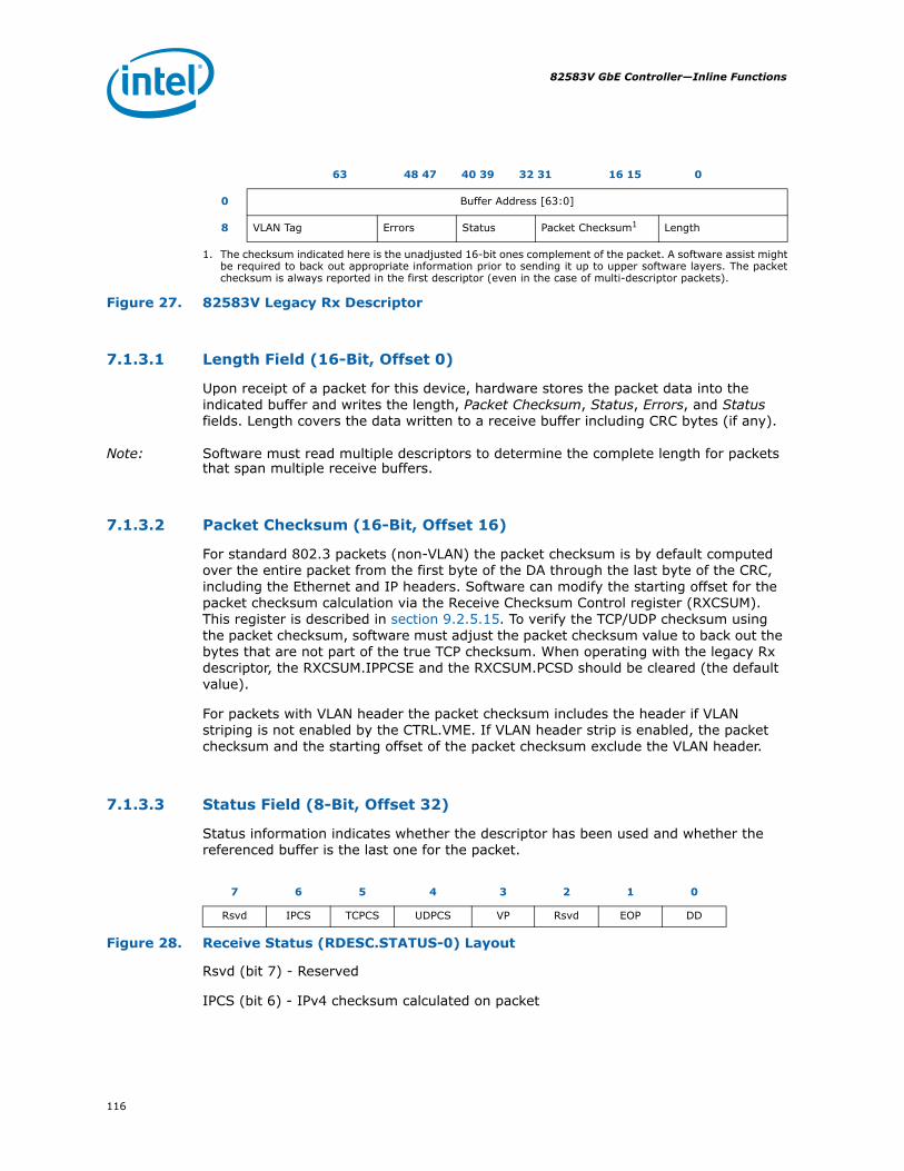
82583V GbE Controller—Inline Functions
116
Figure 27. 82583V Legacy Rx Descriptor
7.1.3.1 Length Field (16-Bit, Offset 0)
Upon receipt of a packet for this device, hardware stores the packet data into the indicated buffer and writes the length, Packet Checksum, Status, Errors, and Status fields. Length covers the data written to a receive buffer including CRC bytes (if any).
Note: Software must read multiple descriptors to determine the complete length for packets that span multiple receive buffers.
7.1.3.2 Packet Checksum (16-Bit, Offset 16)
For standard 802.3 packets (non-VLAN) the packet checksum is by default computed over the entire packet from the first byte of the DA through the last byte of the CRC, including the Ethernet and IP headers. Software can modify the starting offset for the packet checksum calculation via the Receive Checksum Control register (RXCSUM). This register is described in section 9.2.5.15. To verify the TCP/UDP checksum using the packet checksum, software must adjust the packet checksum value to back out the bytes that are not part of the true TCP checksum. When operating with the legacy Rx descriptor, the RXCSUM.IPPCSE and the RXCSUM.PCSD should be cleared (the default value).
For packets with VLAN header the packet checksum includes the header if VLAN striping is not enabled by the CTRL.VME. If VLAN header strip is enabled, the packet checksum and the starting offset of the packet checksum exclude the VLAN header.
7.1.3.3 Status Field (8-Bit, Offset 32)
Status information indicates whether the descriptor has been used and whether the referenced buffer is the last one for the packet.
Figure 28. Receive Status (RDESC.STATUS-0) Layout
Rsvd (bit 7) - Reserved
IPCS (bit 6) - IPv4 checksum calculated on packet
63 48 47 40 39 32 31 16 15 0
0 Buffer Address [63:0]
8 VLAN Tag Errors Status Packet Checksum1
1. The checksum indicated here is the unadjusted 16-bit ones complement of the packet. A software assist mightbe required to back out appropriate information prior to sending it up to upper software layers. The packetchecksum is always reported in the first descriptor (even in the case of multi-descriptor packets).
Length
7 6 5 4 3 2 1 0
Rsvd IPCS TCPCS UDPCS VP Rsvd EOP DD

117
Inline Functions—82583V GbE Controller
TCPCS (bit 5) - TCP checksum calculated on packet
UDPCS (bit 4) - UDP checksum calculated on packet
VP (bit 3) - Packet is 802.1q (matched VET)
Reserved (bit 2) - Reserved
EOP (bit 1) - End of packet
DD (bit 0) - Descriptor done
EOP: Packets that exceed the receive buffer size spans multiple receive buffers. EOP indicates whether this is the last buffer for an incoming packet. DD indicates whether hardware is done with the descriptor. When the DD bit is set along with EOP, the received packet is completely in main memory. Software can determine buffer usage by setting the status byte to zero before making the descriptor available to hardware, and checking it for non-zero content at a later time. For multi-descriptor packets, packet status is provided in the final descriptor of the packet (EOP set). If EOP is not set for a descriptor, only the Address, Length, and DD bits are valid.
VP: The VP field indicates whether the incoming packet's type matches VET (for example, if the packet is a VLAN (802.1q) type). It is set if the packet type matches VET and CTRL.VME is set. For a further description of 802.1q VLANs, see section 7.5.
IPCS TCPCS UDPCS: These bit descriptions are listed in the following table:
IPv6 packets do not have the IPCS bit set, but might have the TCPCS bit set if the 82583V recognized the TCP or UDP packet.
7.1.3.4 Error Field (8-Bit, Offset 40)
Most error information appears only when the Store-Bad-Packet bit (RCTL.SBP) is set and a bad packet is received. Figure 29 shows the definition of the possible errors and their bit positions.
Figure 29. Receive Errors (RDESC.ERRORS) Layout
RXE (bit 7) - Rx data error
IPE (bit 6) - IPv4 checksum error
TCPCS UDPCS IPCS Functionality
0b 0b 0b Hardware does not provide checksum offload.
1b 0b 1b/0bHardware provides IPv4 checksum offload if IPCS active and TCP checksum offload. Pass/fail indication is provided in the Error field – IPE and TCPE.
1b 1b 1b/0bHardware provides IPv4 checksum offload if IPCS active and UDP checksum offload. Pass/Fail indication is provided in the Error field – IPE and TCPE.
7 6 5 4 3 2 1 0
RXE IPE TCPE CXE Rsv SEQ SE CE

82583V GbE Controller—Inline Functions
118
TCPE (bit 5) - TCP/UDP checksum error
CXE (bit 4) - Carrier extension error
Rsv (bit 3) - Reserved
SEQ (bit 2) - Sequence error
SE (bit 1) - Symbol error
CE (bit 0) - CRC error or alignment error
The IP and TCP checksum error bits are valid only when the IPv4 or TCP/UDP checksum(s) is performed on the received packet as indicated via IPCS and TCPCS previously mentioned. These, along with the other error bits, are valid only when the EOP and DD bits are set in the descriptor.
Note: Receive checksum errors have no effect on packet filtering.
If receive checksum offloading is disabled (RXCSUM.IPOFL and RXCSUM.TUOFL), the IPE and TCPE bits are 0b.
The RXE bit indicates that a data error occurred during the packet reception that has been detected by the PHY. This generally corresponds to signal errors occurring during the packet reception. This bit is valid only when the EOP and DD bits are set and are not set in descriptors unless RCTL.SBP (Store-Bad-Packets) is set.
CRC errors and alignment errors are both indicated via the CE bit. Software can distinguish between these errors by monitoring the respective statistics registers.
7.1.3.5 VLAN Tag Field (16-Bit, Offset 48)
Hardware stores additional information in the receive descriptor for 802.1q packets. If the packet type is 802.1q (determined when a packet matches VET and RCTL.VME = 1b), then the VLAN Tag field records the VLAN information and the four-byte VLAN information is stripped from the packet data storage. Otherwise, the VLAN Tag field contains 0x0000.
7.1.4 Extended Rx Descriptor
If the RFCTL.EXSTEN bit is set and RCTL.DTYP equals 00b, the 82583V uses the extended Rx descriptor as follows:
Descriptor Read Format:
15 13 12 11 0
PRI CFI VLAN
63 0
0 Buffer Address [63:0]
8 Reserved 0

119
Inline Functions—82583V GbE Controller
7.1.4.1 Buffer Address (64-Bit, Offset 0.0)
The field contains the physical address of the receive data buffer. The size of the buffer is defined by the RCTL register (RCTL.BSIZE, RCTL.BSEX, RCTL.DTYP and RCTL. FLXBUF fields).
7.1.4.2 DD (1-Bit, Offset 8.0)
This is the location of the DD bit in the Status field. The software device driver must clear this bit before it handles the receive descriptor to the 82583V. The software device driver can use this bit field later on as a completion indication of the hardware.
Descriptor Write-Back Format:
Note: Light-blue fields are mutually exclusive by RXCSUM.PCSD
7.1.4.3 MRQ Field (32-Bit, Offset 0.0)
7.1.4.4 Packet Checksum (16-Bit, Offset 0.48)
For standard 802.3 packets (non-VLAN) the packet checksum is by default computed over the entire packet from the first byte of the DA through the last byte of the CRC, including the Ethernet and IP headers. Software can modify the starting offset for the packet checksum calculation via the Receive Checksum Control register (RXCSUM). This register is described in section 9.2.5.15. To verify the TCP/UDP checksum using the packet checksum, software must adjust the packet checksum value to back out the bytes that are not part of the true TCP checksum. Likewise, for fragmented UDP packets, the Packet Checksum field can be used to accelerate UDP checksum verification by the host processor. This operation is enabled by the RXCSUM.IPPCSE bit as described in section 9.2.5.15.
For packets with VLAN header the packet checksum includes the header if VLAN striping is not enabled by the CTRL.VME bit. If VLAN header strip is enabled, the packet checksum and the starting offset of the packet checksum exclude the VLAN header.
63 48 47 32 31 20 19 0
0 Reserved MRQ
Packet Checksum IP Identification
8 VLAN Tag Length Extended Error Extended Status
Field Bit(s) Description
Reserved 3:0 Reserved
Reserved 7:4 Reserved
Reserved 12:8 Reserved
Reserved 31:13 Reserved

82583V GbE Controller—Inline Functions
120
7.1.4.5 IP Identification (16-Bit, Offset 0.32)
This field stores the IP Identification field in the IP header of the incoming packet. The software device driver should ignore this field when IPIDV is not set.
7.1.4.6 Extended Status (20-Bit, Offset 8.0)
PKTTYPE (bits 19:16) - Packet type
ACK (bit 15) - ACK packet indication
Reserved (bits 14:11) - Reserved
UDPV (bit 10) - Valid UDP XSUM
IPIDV (bit 9) - IP identification valid
TST (bit 8) - Time stamp taken
Rsvd (bit 7) - Reserved
IPCS (bit 6) IPv4 checksum calculated on packet - same as legacy descriptor.
TCPCS (bit 5) - TCP checksum calculated on packet - same as legacy descriptor.
UDPCS (bit 4) - UDP checksum calculated on packet.
VP (bit 3) - Packet is 802.1q (matched VET) - same as legacy descriptor.
Rsv (bit 2) - Reserved
EOP (bit 1) - End of packet - same as legacy descriptor.
DD (bit 0) - Descriptor done - same as legacy descriptor.
DD EOP IXSM VP UDPCS TCPCS IPCS: Same meaning as in the legacy receive descriptor.
9 8 7 6 5 4 3 2 1 0
IPIDV TST Rsvd IPCS TCPCS UDPCS VP Rsvd EOP DD
19 18 17 16 15 14 13 12 11 10
PKTTYPE ACK Reserved UDPV

121
Inline Functions—82583V GbE Controller
IPCS TCPCS UDPCS: The meaning of these bits is shown in the following table:
Unsupported packet types do not have the IPCS or TCPCS bits set. IPv6 packets do not have the IPCS bit set, but might have the TCPCS bit set if the 82583V recognized the TCP or UDP packet.
IPIDV (bit 9): The IPIDV bit indicates that the incoming packet was identified as a fragmented IPv4 packet. The IPID field contains a valid IP identification value if the RXCSUM.PCSD is cleared.
UDPV (bit 10): The UDPV bit indicates that the incoming packet contains a valid (non-zero value) checksum field in an incoming fragmented UDP IPv4 packet. It means that the Packet Checksum field contains the UDP checksum as described in this section. When this field is cleared in the first fragment that contains the UDP header, it means that the packet does not contain a valid UDP checksum and the checksum field in the Rx descriptor should be ignored. This field is always cleared in incoming fragments that do not contain the UDP header.
ACK (bit 15): The ACK bit indicates that the received packet was an ACK packet with or without TCP payload depending on the RFCTL.ACKD_DIS bit.
PKTTYPE (bit 19:16): The PKTTYPE field defines the type of the packet that was detected by the 82583V. The 82583V tries to find the most complex match until the most common one as shown in the following packet type table:
TCPCS UDPCS IPCS Functionality
0b 0b 1b/0b Hardware provides IPv4 checksum offload if IPCS active.
1b 0b 1b/0bHardware provides IPv4 checksum offload if IPCS active and TCP checksum offload. Pass/fail indication is provided in the Error field – IPE and TCPE.
0b 1b 1b/0b
For IPv4 packets, hardware provides IP checksum offload if IPCS active and fragmented UDP checksum offload. IP Pass/fail indication is provided in the IPE field. Fragmented UDP checksum is provided in the packet checksum field if the RXCSUM.PCSD bit is cleared.
1b 1b 1b/0bHardware provides IPv4 checksum offload if IPCS active and UDP checksum offload. Pass/fail indication is provided in the Error field – IPE and TCPE.
Packet Type Description
0x0 MAC, (VLAN/SNAP) payload
0x1 MAC, (VLAN/SNAP) IPv4, payload
0x2 MAC, (VLAN/SNAP) IPv4, TCP/UDP, payload
0x3 MAC (VLAN/SNAP), IPv4, IPv6, payload
0x4 MAC (VLAN/SNAP), IPv4, IPv6, TCP/UDP, payload
0x5 MAC (VLAN/SNAP), IPv6, payload
0x6 MAC (VLAN/SNAP), IPv6,TCP/UDP, payload
0x7 MAC, (VLAN/SNAP), IPv4, TCP, ISCSI, payload
0x8 MAC, (VLAN/SNAP), IPv4, TCP/UDP, NFS, payload
0x9 MAC (VLAN/SNAP), IPv4, IPv6,TCP, ISCSI, payload
0xA MAC (VLAN/SNAP), IPv4, IPv6,TCP/UDP,NFS, payload
0xB MAC (VLAN/SNAP), IPv6,TCP, ISCSI, payload

82583V GbE Controller—Inline Functions
122
— Payload does not mean raw data but can also be unsupported header.— If there is an NFS/iSCSI header in the packets it can be seen in the packet type
field.
Note: If the device is not configured to provide any offload that requires packet parsing, the packet type field is set to 0b regardless of the actual packet type.
7.1.4.7 Extended Errors (12-Bit, Offset 8.20)
RXE (bit 11) - Rx data error - Same as legacy descriptor.
IPE (bit 10) - IPv4 checksum error - Same as legacy descriptor.
TCPE (bit 9) - TCP/UDP checksum error - Same as legacy descriptor.
CXE (bit 8) - Carrier extension error - Same as legacy descriptor.
SEQ (bit 6) - Sequence error - Same as legacy descriptor.
SE (bit 5) - Symbol error - Same as legacy descriptor.
CE (bit 4) - CRC error or alignment error - Same as legacy descriptor.
Reserved (bits 7, 3:0) - Reserved
RXE IPE TCPE CXE SEQ SE CE: Same as legacy descriptor.
Length (16-bit, offset 8.32): Same as the length field at offset 8.0 in the legacy descriptor.
VLAN Tag (16-bit, offset 8.48): Same as legacy descriptor.
7.1.4.7.1 Receive UDP Fragmentation Checksum
The 82583V might provide receive fragmented UDP checksum offload. The following setup should be made to enable this mode:
RXCSUM.PCSD bit should be cleared. When the PCSD bit is cleared, Packet Checksum and IP Identification are active.
RXCSUM.IPPCSE bit should be set. This field enables the IP payload checksum enable that is designed for the fragmented UDP checksum.
Packet Type Description
0xC MAC (VLAN/SNAP), IPv6,TCP/UDP, NFS, payload
0xD Reserved
0xE Reserved
11 10 9 8 7 6 5 4 3 2 1 0
RXE IPE TCPE CXE Rsvd SEQ SE CE Rsvd Rsvd

123
Inline Functions—82583V GbE Controller
RXCSUM.PCSS field must be zero. The packet checksum start should be zero to enable auto start of the checksum calculation. See the following table for an exact description of the checksum calculation.
The following table lists the outcome descriptor fields for the following incoming packets types:
Note: When the software device driver computes the 16-bit ones complement sum on the incoming packets of the UDP fragments, it should expect a value of 0xFFFF. See section 7.1.10 for supported packet formats.
7.1.5 Packet Split Receive Descriptor
The 82583V uses the packet split feature when the RFCTL.EXSTEN bit is set and RCTL.DTYP=01b. The software device driver must also program the buffer sizes in the PSRCTL register.
Descriptor Read Format:
Incoming Packet Type Packet Checksum IP
Identification UDPV/IPIDV UDPCS/TCPCS
None IPv4 Packet
Unadjusted 16-bit ones complement checksum of the entire packet (excluding VLAN header)
Reserved 0b/0b 0b/0b
Fragment IPv4 with TCP header
Same as above Incoming IP Identification 0b/1b 0b/0b
Non- fragmented IPv4 packet
Same as above Reserved 0b/0bDepend on transport header and TUOFL field
Fragmented IPv4 without transport header
The unadjusted 1’s complement checksum of the IP payload
Incoming IP Identification 0b/1b 1b/0b
Fragmented IPv4 with UDP header
Same as above Incoming IP Identification
1b if the UDP header checksum is valid/1b
1b/0b
63 0
0 Buffer Address 0
8 Buffer Address 1 0
16 Buffer Address 2
24 Buffer Address 3

82583V GbE Controller—Inline Functions
124
7.1.5.1 Buffer Addresses [3:0] (4 x 64 bit)
The physical address of each buffer is written in the Buffer Addresses fields. The sizes of these buffers are statically defined by BSIZE0-BSIZE3 in the PSRCTL register.
Note: Software Notes:• All buffers' addresses in a packet split descriptor must be word aligned.• Packet header can't span across buffers, therefore, the size of the first buffer must
be larger than any expected header size. Otherwise the packet will not be split.• If software sets a buffer size to zero, all buffers following that one should be set to
zero as well. Pointers in the packet split receive descriptors to buffers with a zero size should be set to any address, but not to NULL pointers. Hardware does not write to this address.
• When configured to packet split and a given packet spans across two or more packet split descriptors, the first buffer of any descriptor (other than the first one) is not used.
7.1.5.2 DD (1-Bit, Offset 8.0)
The software device driver might use the DD bit from the Status field to determine when a descriptor has been used. Therefore, the software device driver must ensure that the Least Significant B (LSB) of Buffer Address 1 is zero. This should not be an issue, since the buffers should be page aligned for the packet split feature to be useful.
Note: Any software device driver that cannot align buffers should not be using this descriptor format.

125
Inline Functions—82583V GbE Controller
Descriptor Write-Back Format:
Note: Light-blue fields are mutually exclusive by RXCSUM.PCSD
MRQ - Same as extended Rx descriptor.
Packet Checksum, IP Identification - Same as extended Rx descriptor.
Extended Status, Extended Errors, VLAN Tag - Same as extended Rx descriptor.
7.1.5.3 Length 0 (16-Bit, Offset 8.32), Length [3:1] (3- x 16-Bit, Offset 16.16)
Upon a packet reception, hardware stores the packet data in one or more of the indicated buffers. Hardware writes in the Length field of each buffer the number of bytes that were posted in the corresponding buffer. If no packet data is stored in a given buffer, hardware writes 0b in the corresponding Length field. Length covers the data written to receive buffer including CRC bytes (if any).
Software is responsible for checking the Length fields of all buffers for data that hardware might have written to the corresponding buffers.
Note: The larger buffer sizes are only offered to provide compatibility with other silicon types. Jumbo frames are not supported with the 82583V.
7.1.5.4 Header Status (16-Bit, Offset 16.0):
HDRSP (bit 15) - Headers were split
Reserved (bits 14:10) - Reserved
Header Length (bits 9:0) - Packet header length
63 48 47 32 31 20 19 16 15 0
0 Reserved MRQ
Packet Checksum IP Identification
8 VLAN Tag Length 0 Extended Error Extended Status
16 Length 3 Length 2 Length 1 Header Status
24 Reserved
15 14 10 9 0
HDRSP Reserved HLEN (Header Length)

82583V GbE Controller—Inline Functions
126
HDRSP (bit 15): The HDRSP bit (when active) indicates that hardware split the headers from the packet data for the packet contained in this descriptor. The following table identifies the packets that are supported by header/data split functionality. In addition, packets with a data portion smaller than 16 bytes are not guaranteed to be split. If the device is not configured to provide any offload that requires packet parsing, the HDRSP bit is set to 0b' even if packet split was enabled. Non-split packets are stored linearly in the buffers of the receive descriptor.
HLEN (bit 9:0): The HLEN field indicates the header length in byte count that was analyzed by the 82583V. The 82583V posts the first HLEN bytes of the incoming packet to buffer zero of the Rx descriptor.
Packet types supported by the packet split: The 82583V provides header split for the packet types listed in the following table. Other packet types are posted sequentially in the buffers of the packet split receive buffers.
Note: A header of a fragmented IPv6 packet is defined until the fragmented extension header.
Packet Type Description Header Split
0x0 MAC, (VLAN/SNAP), payload No.
0x1 MAC, (VLAN/SNAP), IPv4, payload Split header after L3 if fragmented packets.
0x2 MAC, (VLAN/SNAP), IPv4, TCP/UDP, payload Split header after L4 if not fragmented, otherwise treat as packet type 1.
0x3 MAC (VLAN/SNAP), IPv4, IPv6, payload Split header after L3 if either IPv4 or IPv6 indicates a fragmented packet.
0x4 MAC (VLAN/SNAP), IPv4, IPv6,TCP/UDP, payload
Split header after L4 if IPv4 not fragmented and if IPv6 does not include fragment extension header, otherwise treat as packet type 3.
0x5 MAC (VLAN/SNAP), IPv6, payload Split header after L3 if fragmented packets.
0x6 MAC (VLAN/SNAP), IPv6,TCP/UDP, payloadSplit header after L4 if IPv6 does not include fragment extension header, otherwise treat as packet type 5.
0x7 MAC, (VLAN/SNAP) IPv4, TCP, ISCSI, payload Split header after L5 if not fragmented, otherwise treat as packet type 1.
0x8 MAC, (VLAN/SNAP) IPv4, TCP/UDP, NFS, payload Split header after L5 if not fragmented, otherwise treat as packet type 1.
0x9 MAC (VLAN/SNAP), IPv4, IPv6, TCP, ISCSI, payload
Split header after L5 if IPv4 not fragmented and if IPv6 does not include fragment extension header, otherwise treat as packet type 3.
0xA MAC (VLAN/SNAP), IPv4, IPv6, TCP/UDP,NFS, payload
Split header after L5 if IPv4 not fragmented and if IPv6 does not include fragment extension header, otherwise treat as packet type 3.
0xB MAC (VLAN/SNAP), IPv6, TCP, ISCSI, payloadSplit header after L5 if IPv6 does not include fragment extension header, otherwise treat as packet type 5.
0xC MAC (VLAN/SNAP), IPv6, TCP/UDP, NFS, payloadSplit header after L5 if IPv6 does not include fragment extension header, otherwise treat as packet type 5.
0xD Reserved
0xE Reserved
127
Inline Functions—82583V GbE Controller
Note: If the device is not configured to provide any offload that requires packet parsing, the packet type field is set to 0b regardless of the actual packet type. When packet split is enabled, the packet type field is always valid.
7.1.6 Receive Descriptor Fetching
The fetching algorithm attempts to make the best use of PCIe bandwidth by fetching a cache-line (or more) descriptor with each burst. The following paragraphs briefly describe the descriptor fetch algorithm and the software control provided.
When the on-chip buffer is empty, a fetch happens as soon as any descriptors are made available (host writes to the tail pointer). When the on-chip buffer is nearly empty (RXDCTL.PTHRESH), a prefetch is performed each time enough valid descriptors (RXDCTL.HTHRESH) are available in host memory and no other PCIe activity of greater priority is pending (descriptor fetches and write backs or packet data transfers).
When the number of descriptors in host memory is greater than the available on-chip descriptor storage, the chip might elect to perform a fetch that is not a multiple of cache line size. The hardware performs this non-aligned fetch if doing so results in the next descriptor fetch being aligned on a cache line boundary. This enables the descriptor fetch mechanism to be most efficient in the cases where it has fallen behind software.
Note: The 82583V NEVER fetches descriptors beyond the descriptor tail pointer.
7.1.7 Receive Descriptor Write Back
Processors have cache line sizes that are larger than the receive descriptor size (16 bytes). Consequently, writing back descriptor information for each received packet can cause expensive partial cache line updates. Two mechanisms minimize the occurrence of partial line write backs:
• Receive descriptor packing• Null descriptor padding
The following sections explain these mechanisms.
7.1.7.1 Receive Descriptor Packing
To maximize memory efficiency, receive descriptors are packed together and written as a cache line whenever possible. Descriptors accumulate and are opportunistically written out in cache line-oriented chunks. Used descriptors are also explicitly written out under the following scenarios:
• RXDCTL.WTHRESH descriptors have been used (the specified maximum threshold of unwritten used descriptors has been reached)
• The last descriptors of the allocated descriptor ring have been used (to enable hardware to re-align to the descriptor ring start)
• A receive timer expires (RADV or RDTR) • Explicit software flush (RDTR.FPD)

82583V GbE Controller—Inline Functions
128
When the number of descriptors specified by RXDCTL.WTHRESH have been used, they are written back, regardless of cache line alignment. It is therefore recommended that WTHRESH be a multiple of cache line size. When a receive timer (RADV or RDTR) expires, all used descriptors are forced to be written back prior to initiating the interrupt, for consistency. Software might explicitly flush accumulated descriptors by writing the RDTR register with the high order bit (FPD) set.
7.1.7.2 Null Descriptor Padding
Hardware stores no data in descriptors with a null data address. Software can make use of this property to cause the first condition under receive descriptor packing to occur early. Hardware writes back null descriptors with the DD bit set in the status byte and all other bits unchanged.
Note: Null descriptor padding is not supported for packet split descriptors.
7.1.8 Receive Descriptor Queue Structure
Figure 30 shows the structure of the receive descriptor ring. Hardware maintains a circular queue of descriptors and writes back used descriptors just prior to advancing the head pointer. Head and tail pointers wrap back to base when size descriptors have been processed.
Figure 30. Receive Descriptor Ring Structure
Circular Buffer Queues
Head
Base + Size
Base
Receive Queue
Tail

129
Inline Functions—82583V GbE Controller
Software adds receive descriptors by advancing the tail pointer to refer to the address of the entry just beyond the last valid descriptor. This is accomplished by writing the descriptor tail register with the offset of the entry beyond the last valid descriptor. The hardware adjusts its internal tail pointer accordingly. As packets arrive, they are stored in memory and the head pointer is incremented by hardware. When the head pointer is equal to the tail pointer, the queue is empty. Hardware stops storing packets in system memory until software advances the tail pointer, making more receive buffers available.
The receive descriptor head and tail pointers reference 16-byte blocks of memory. Shaded boxes in the figure represent descriptors that have stored incoming packets but have not yet been recognized by software. Software can determine if a receive buffer is valid by reading descriptors in memory rather than by I/O reads. Any descriptor with a non-zero status byte has been processed by the hardware, and is ready to be handled by the software.
Note: When configured to work as a packet split feature, the descriptor tail needs to be increment by software by two for every descriptor ready in memory (as the packet split descriptors are 32 bytes while regular descriptors are 16 bytes).
Note: The head pointer points to the next descriptor that will be written back. At the completion of the descriptor write-back operation, this pointer is incremented by the number of descriptors written back. Hardware OWNS all descriptors between [head... tail]. Any descriptor not in this range is owned by software.
The receive descriptor ring is described by the following registers:
• Receive Descriptor Base Address registers (RDBA0)— This register indicates the start of the descriptor ring buffer; this 64-bit address
is aligned on a 16-byte boundary and is stored in two consecutive 32-bit registers. Hardware ignores the lower 4 bits.
• Receive Descriptor Length registers (RDLEN0)— This register determines the number of bytes allocated to the circular buffer.
This value must be a multiple of 128 (the maximum cache line size). Since each descriptor is 16 bytes in length, the total number of receive descriptors is always a multiple of 8.
• Receive Descriptor Head register (RDH0)— This register holds a value that is an offset from the base, and indicates the in-
progress descriptor. There can be up to 64 KB descriptors in the circular buffer. Hardware maintains a shadow copy that includes those descriptors completed but not yet stored in memory.
• Receive Descriptor Tail register (RDT0)— This register holds a value that is an offset from the base, and identifies the
location beyond the last descriptor hardware can process. This is the location where software writes the first new descriptor.
If software statically allocates buffers, and uses memory read to check for completed descriptors, it simply has to zero the status byte in the descriptor to make it ready for reuse by hardware. This is not a hardware requirement (moving the hardware tail pointer is), but is necessary for performing an in-memory scan.

82583V GbE Controller—Inline Functions
130
7.1.9 Receive Interrupts
The following indicates the presence of new packets:
• Receive Timer (ICR.RXT0) due to packet delay timer (RDTR)
A predetermined amount of time has elapsed since the last packet was received and transferred to host memory. Every time a new packet is received and transferred to the host memory, the timer is re-initialized to the predetermined value. The timer then counts down and triggers an interrupt if no new packet is received and transferred to host memory completely before the timer expires. Software can set the timer value to zero if it needs to be notified immediately (no interval delay) whenever a new packet has been stored in memory.
Writing the absolute timer with its high order bit set to 1b forces an explicit flush of any partial cache lines worth of consumed descriptors. Hardware writes all used descriptors to memory and updates the globally visible value of the RXDH head pointer.
This timer is re-initialized when an interrupt is generated and restarts when a new packet is observed. It stays disabled until a new packet is received and transferred to the host memory. The packet delay timer is also re-initialized when an interrupt occurs due to an absolute timer expiration or small packet-detection interrupt.
• Receive Timer (ICR.RXT0) due to absolute timer (RADV)
A predetermined amount of time has elapsed since the first packet received after the hardware timer was written (specifically, after the last packet data byte was written to memory).
This timer is re-initialized when an interrupt is generated and restarts when a new packet is observed. It stays disabled until a new packet is received and transferred to the host memory. The absolute delay timer is also re-initialized when an interrupt occurs due to a packet timer expiration or small packet-detection interrupt.
The absolute timer and the packet delay timer can be used together. The following table lists the conditions when the absolute timer and the packet delay timer are initialized, disabled and when they start counting. The timer is always disabled if the value of the RDTR = 0b.
Figure 31 further clarifies the packet timer operation.
Interrupt Timers
When Starts Counting When Re-initialized When Disabled
Absolute delay timer
Timer inactive and receive packet transferred to host memory.
At startOn expirationDue to other receive interrupt.
Packet delay timer
Timer inactive and receive packet transferred to host memory.
At startNew packet received and transferred to host memory
On expirationDue to other receive interrupt.

131
Inline Functions—82583V GbE Controller
Figure 31. Packet Delay Timer Operation (With State Diagram)
Figure 32 shows how the packet timer and absolute timer can be used together:
DISABLED
RUNNING
packet received & xferred to host mem
Action: Re-initialized
packet received & xfer to host memory
Action - Re-initialize
INT GENERATED
Timer expires
other receive interrupts
Initial State

82583V GbE Controller—Inline Functions
132
Figure 32. Packet and Absolute Timers• Small Receive Packet Detect (ICR.SRPD)
— A receive interrupt is asserted when small-packet detection is enabled (RSRPD is set with a non-zero value) and a packet of (size < RSRPD.SIZE) has been transferred into the host memory. When comparing the size the headers and CRC are included (if CRC stripping is not enabled). CRC and VLAN headers are not included if they have been stripped. A receive timer interrupt cause (ICR.RXT0) will also be noted when the small packet-detect interrupt occurs.
• Receive ACK frame interrupt is asserted when a frame is detected to be an ACK frame. Detection of ACK frames are masked through the IMS register. When a frame is detected as an ACK frame an interrupt is asserted after the RAID.ACK_DELAY timer had expired and the ACK frames interrupts were not masked in the IMS register.
Note: The ACK frame detect feature is only active when configured to packet split (RCTL.DTYP=01b) or the extended status feature is enabled (RFCTL.EXSTEN is set).
A bsolute Timer Value
PKT #1 PKT #2 PKT #3 PKT #4Interrupt generated due to PKT #1
A bsolute Timer Value
PKT #1 PKT #2 PKT #3 PKT #4
Interrupt generalted (due to PKT #4) as absolute timer expires.Packet delay timer disabled untill next packet is received and transferred to host memory.
PKT #5 PKT #6 ... ... ...
A bsolute Timer Value
1) Packet timer expires2) Interrupt generated3) Absolute timer reset
A bsolute Timer Value
PKT #1 PKT #2 PKT #3 PKT #4
Interrupt generalted (due to PKT #4) as absolute timer expires.Packet delay timer disabled untill next packet is received and transferred to host memory.
PKT #5 PKT #6 ... ... ...
A bsolute Timer Value
1) Packet timer expires2) Interrupt generated3) Absolute timer reset
Case A: Using only an absolute timer
Case B: Using an absolute time in conjunction with the Packet timer
Case C: Packet timer expiring while a packet is transferred to host memory.Illustrates that packet timer is re-started only after a packet is transferred to host memory.

133
Inline Functions—82583V GbE Controller
Receive interrupts can also be generated for the following events:
• Receive Descriptor Minimum Threshold (ICR.RXDMT)— The minimum descriptor threshold helps avoid descriptor under-run by
generating an interrupt when the number of free descriptors becomes equal to the minimum. It is measured as a fraction of the receive descriptor ring size. This interrupt would stop and re-initialize the entire active delayed receives interrupt timers until a new packet is observed.
• Receiver FIFO Overrun (ICR.RXO)— FIFO overrun occurs when hardware attempts to write a byte to a full FIFO. An
overrun could indicate that software has not updated the tail pointer to provide enough descriptors/buffers, or that the PCIe bus is too slow draining the receive FIFO. Incoming packets that overrun the FIFO are dropped and do not affect future packet reception. This interrupt would stop and re-initialize the entire active delayed receives interrupts.
7.1.10 Receive Packet Checksum Offloading
The 82583V supports the offloading of three receive checksum calculations: the packet checksum, the IPv4 header checksum, and the TCP/UDP checksum.
The packet checksum is the one's complement over the receive packet, starting from the byte indicated by RXCSUM.PCSS (zero corresponds to the first byte of the packet), after stripping. For packets with VLAN header the packet checksum includes the header if VLAN striping is not enabled by the CTRL.VME. If VLAN header strip is enabled, the packet checksum and the starting offset of the packet checksum exclude the VLAN header due to masking of VLAN header. For example, for an Ethernet II frame encapsulated as an 802.3ac VLAN packet and CTRL.VME is set and with RXCSUM.PCSS set to 14, the packet checksum would include the entire encapsulated frame, excluding the 14-byte Ethernet header (DA, SA, Type/Length) and the 4-byte q-tag. The packet checksum does not include the Ethernet CRC if the RCTL.SECRC bit is set.
Software must make the required offsetting computation (to back out the bytes that should not have been included and to include the pseudo-header) prior to comparing the packet checksum against the TCP checksum stored in the packet.
For supported packet/frame types, the entire checksum calculation can be offloaded to the 82583V. If RXCSUM.IPOFLD is set to 1b, the 82583V calculates the IPv4 checksum and indicates a pass/fail indication to software via the IPv4 Checksum Error bit (RDESC.IPE) in the Error field of the receive descriptor. Similarly, if RXCSUM.TUOFLD is set to 1b, the 82583V calculates the TCP or UDP checksum and indicates a pass/fail condition to software via the TCP/UDP Checksum Error bit (RDESC.TCPE). These error bits are valid when the respective status bits indicate the checksum was calculated for the packet (RDESC.IPCS and RDESC.TCPCS respectively). Similarly, if RFCTL.Ipv6_DIS and RFCTL.IP6Xsum_DIS are cleared to 0b and RXCSUM.TUOFLD is set to 1b, the 82583V calculates the TCP or UDP checksum for IPv6 packets. It then indicates a pass/fail condition in the TCP/UDP Checksum Error bit (RDESC.TCPE).
If neither RXCSUM.IPOFLD nor RXCSUM.TUOFLD are set, the Checksum Error bits (IPE and TCPE) are 0b for all packets.
82583V GbE Controller—Inline Functions
134
Supported frame types:
• Ethernet II• Ethernet SNAP
Table 38. Supported Receive Checksum Capabilities
The previous table lists the general details about what packets are processed. In more detail, the packets are passed through a series of filters to determine if a receive checksum is calculated:
7.1.10.1 MAC Address Filter
This filter checks the MAC destination address to be sure it is valid (such as, IA match, broadcast, multicast, etc.). The receive configuration settings determine which MAC addresses are accepted. See the various receive control configuration registers such as RCTL (RTCL.UPE, RCTL.MPE, RCTL.BAM), MTA, RAL, and RAH.
7.1.10.2 SNAP/VLAN Filter
This filter checks the next headers looking for an IP header. It is capable of decoding Ethernet II, Ethernet SNAP, and IEEE 802.3ac headers. It skips past any of these intermediate headers and looks for the IP header. The receive configuration settings determine which next headers are accepted. See the various receive control configuration registers such as RCTL (RCTL.VFE), VET, and VFTA.
Packet Type HW IP Checksum Calculation
HW TCP/UDP Checksum Calculation
IPv4 packets Yes Yes
IPv6 packets No (n/a) Yes
IPv6 packet with next header options:Hop-by-Hop optionsDestinations optionsRouting (with len 0)Routing (with len >0)FragmentHome option
No (n/a)No (n/a)No (n/a)No (n/a)No (n/a)No (n/a)
YesYesYesNoNoNo
IPv4 tunnels: IPv4 packet in an IPv4 tunnel IPv6 packet in an IPv4 tunnel
NoYes (IPv4)
NoYes1
1. The IPv6 header portion can include supported extension headers as described in the IPv6 filter section.
IPv6 tunnels: IPv4 packet in an IPv6 tunnel IPv6 packet in an IPv6 tunnel
NoNo
NoNo
Packet is an IPv4 fragment Yes No
Packet has 802.3ac tag Yes Yes
IPv4 Packet has IP options(IP header is longer than 20 bytes)
Yes Yes
Packet has TCP or UDP options Yes Yes
IP header’s protocol field contains a protocol # other than TCP or UDP. Yes No
135
Inline Functions—82583V GbE Controller
7.1.10.3 IPv4 Filter
This filter checks for valid IPv4 headers. The version field is checked for a correct value (4).
IPv4 headers are accepted if they are any size greater than or equal to 5 (Dwords). If the IPv4 header is properly decoded, the IP checksum is checked for validity. The RXCSUM.IPOFL bit must be set for this filter to pass.
7.1.10.4 IPv6 Filter
This filter checks for valid IPv6 headers, which are a fixed size and have no checksum. The IPv6 extension headers accepted are: hop-by-hop, destination options, and routing. The maximum size next header accepted is 16 Dwords (64 bytes).
All of the IPv6 extension headers supported by the 82583V have the same header structure:
NEXT HEADER is a value that identifies the header type. The supported IPv6 next headers values are:
• Hop-by-hop = 0x00• Destination options = 0x3C• Routing = 0x2B
HDR EXT LEN is the 8-byte count of the header length, not including the first 8 bytes. For example, a value of three means that the total header size including the NEXT HEADER and HDR EXT LEN fields is 32 bytes (8 + 3*8).
The RFCTL.Ipv6_DIS bit must be cleared for this filter to pass.
7.1.10.5 UDP/TCP Filter
This filter checks for a valid UDP or TCP header. The prototype next header values are 0x11 and 0x06, respectively. The RXCSUM.TUOFL bit must be set for this filter to pass.
7.2 Packet Transmission
7.2.1 Transmit Functionality
The 82583V transmit flow is a descriptor-based transmit where the hardware gets the per-packet details for the transmit tasks through descriptors created by software.
This section outlines the transmit structures and process along with features and offloads supported by the 82583V.
Byte0 Byte1 Byte2 Byte3
NEXT HEADER HDR EXT LEN

82583V GbE Controller—Inline Functions
136
7.2.2 Transmission Flow Using Simplified Legacy Descriptors
7.2.3 Transmission Process Flow Using Extended Descriptors
The 82583V supports extended Tx descriptors that provide more offload capabilities. The extended offload capabilities are indicated to the hardware by two types of descriptors: context descriptors and data descriptors. The context descriptors define a set of offload capabilities applicable for multiple packets while the data descriptors define the data buffers and specific off load capabilities per packet.
The software/hardware flow while using the extended descriptors is as follows:
• Software prepares the context descriptor that defines the offload capabilities for the incoming packets.
• Software prepares the data packets in host memory within one or more data buffers and their descriptors.
• All steps are the same as the legacy Tx descriptors as previously described (starting at step number 4) while the data buffers belong to a single packet.
The software/hardware flow for TCP segmentation using the extended descriptors is as follows:
• Software prepares the context descriptor that defines the upcoming TCP segmentation, In this case, the data buffers belong to multiple packets.
• Software places a prototype header in host memory and indicates it to the hardware by a data descriptor.
1Software defines a descriptor ring and configures the 82583V's transmit queue with the address location, length, head, and tail pointers of the ring. See section 7.2.4 for more details on the descriptor ring structure.
2 Software prepares the packet headers and data for the transmit within one or more data buffers.
3
Software prepares Tx descriptors according to the number of data buffers that are used. Each descriptor points to a different data buffer and holds the required hardware processing. See section 7.2.9 for more details on the descriptor format. The software places the descriptors in the correct location in the Tx descriptor ring.
4 Software updates the transmit descriptor tail pointer (TDT) to indicate the hardware that Tx descriptors are ready.
5 Hardware senses a change of the TDT and initiates a PCIe request to fetch the descriptors from host memory.
6 The descriptors’ content is received in a PCIe read completion and is written to the appropriate location in the descriptor queue.
7
According to the descriptors content the corresponding memory data buffers are then fetched from the host to the hardware on-chip transmit FIFO.While the packet is passing through the DMA and MAC units, relevant off load functions are incorporated according to the commands in the descriptors.
10 After the entire packet is fetched by the hardware it is transmitted to the Ethernet link.
11After a DMA of each buffer is complete, if the RS bit in the command byte is set, the DMA updates the Status field of the appropriate descriptor and writes back the descriptor to the descriptor ring in host memory.
12 The hardware moves the transmit descriptor head pointer (TDH) in the direction of the tail to point to the next descriptor in the ring.
13 After the entire packet is fetched by the hardware an interrupt might be generated by the hardware to notify the software device driver that it can release the relevant buffers to the operating system.

137
Inline Functions—82583V GbE Controller
• Software places the rest of the data to be transmitted in the host memory indicated to the hardware by additional data descriptors.
• Hardware splits the data into multiple packets according to the Maximum Segment Size (MSS) defined in the context descriptor. Hardware uses the prototype header for each packet while it auto-updates some of the fields in the IP and TCP headers. See more details in section 7.3.6.2.
• For each packet, the proceeding steps are the same as the legacy Tx descriptors as previously described (starting at step number 4).
7.2.4 Transmit Descriptor Ring Structure
The transmit descriptor ring is described by the following registers:
• Transmit Descriptor Base Address register (TDBA)— This register indicates the start address of the descriptor ring buffer in the host
memory; this 64-bit address is aligned on a 16-byte boundary and is stored in two consecutive 32-bit registers. Hardware ignores the lower four bits.
• Transmit Descriptor Length register (TDLEN)— This register determines the number of bytes allocated to the circular ring. This
value must be aligned to 128 bytes.• Transmit Descriptor Head register (TDH)
— This register holds an index value that indicates the in-progress descriptor. There can be up to 64 KB descriptors in the circular buffer. Reading this register returns the value of head corresponding to descriptors already loaded in the transmit FIFO.
• Transmit Descriptor Tail register (TDT)— This register holds a value, which is an offset from the base (TDBA), and
indicates the location beyond the last descriptor hardware can process. This is the location where software writes the next new descriptor.
Figure 33. Transmit Descriptor Ring Structure
BaseTDBA
Base+1
Base + TDLEN
HeadTDH
TailTDT

82583V GbE Controller—Inline Functions
138
Descriptors between the head and the tail pointers are descriptors that have been prepared by software and are owned by hardware.
7.2.4.1 Transmit Descriptor Fetching
The descriptor processing strategy for transmit descriptors is essentially the same as for receive descriptors.
When the on-chip descriptor queue is empty, a fetch occurs as soon as any descriptors are made available (host writes to the tail pointer). Hardware might elect to perform a fetch which is not a multiple of cache line size. The hardware performs this non-aligned fetch if doing so results in the next descriptor fetch being aligned on a cache line boundary. This enables the descriptor fetch mechanism to be most efficient in the cases where it has fallen behind software.
After the initial fetch of descriptors, as the on-chip buffer empties, the hardware can decide to pre-fetch more transmit descriptors if the number of on-chip descriptors drop below TXDCTL.PTHRESH and enough valid descriptors TXDCT is performed.
Note: The 82583V NEVER fetches descriptors beyond the descriptor tail pointer.
7.2.4.2 Transmit Descriptor Write Back
The descriptor write-back policy for transmit descriptors is similar to that for receive descriptors with a few additional factors.
There are three factors: the Report Status (RS) bit in the transmit descriptor, the write back threshold (TXDCTL.WTHRESH) and the Interrupt Delay Enable (IDE) bit in the transmit descriptor.
Descriptors are written back in one of three cases:
• TXDCTL.WTHRESH = zero, IDE = zero and a descriptor with RS set to 1b is ready to be written back, for this condition write backs are immediate. The device writes back only the status byte of the descriptor (TDESCR.STA) and all other bytes of the descriptor are left unchanged.
• IDE = 1b and the Transmit Interrupt Delay (TIDV) register timer expires, this timer is used to force a timely write back of descriptors. Timer expiration flushes any accumulated descriptors and sets an interrupt event.
• TXDCTL.WTHRESH > zero and the write back of the full descriptors are performed only when TXDCTL.WTHRESH number of descriptors are ready for a write back.
139
Inline Functions—82583V GbE Controller
7.2.4.3 Determining Completed Frames as Done
Software can determine if a packet has been sent by the following method:
• Setting the RS bit in the transmit descriptor command field and checking the DD bit of the relevant descriptors in host memory.
The process of checking for completed descriptors consists of the following:
• The software device driver scans the host memory for the value of the DD status bit. When the DD bit =1b, indicates a completed packet, and also indicates that all packets preceding that packet have been put in the output FIFO.
7.2.5 Overview of On-Chip Transmit Modes
Transmit mode is used to refer to a set of configurations that support some of the transmit path offloads. These modes are updated and controlled with the transmit descriptors.
There are three types of transmit modes:
• Legacy mode• Extended mode• Segmentation mode
The first mode (legacy) is an implied mode as it is not explicitly specified with a context descriptor. This mode is constructed by the device from the first and last descriptors of a legacy transmit and from some internal constants. The legacy mode enables insertion of one checksum.
The other two modes are indicated explicitly by a transmit context descriptor. The extended mode is used to control the checksum offloading feature for packet transmission. The segmentation mode is used to control the packet segmentation capabilities of the device. The TSE bit, in the context descriptor, selects which mode is updated, that is, extended mode or segmentation mode. The extended and segmentation modes enable insertion of two checksums. In addition, the segmentation mode adds information specific to the segmentation capability.

82583V GbE Controller—Inline Functions
140
The device automatically selects the appropriate mode to use based on the current packet transmission: legacy, extended, or segmentation.
Note: While the architecture supports arbitrary ordering rules for the various descriptors, there are restrictions including:
— Context descriptors should not occur in the middle of a packet or of a segmentation.
— Data descriptors of different packet types (legacy, extended, or segmentation) should not be intermingled except at the packet (or segmentation) level.
There are dedicated resources on-chip for both the extended and segmentation modes. These modes remain constant until they are modified by another context descriptor. This means that a set of configurations relevant to one mode can (and will) be used for multiple packets unless a new mode is loaded prior to sending a new packet.
7.2.6 Pipelined Tx Data Read Requests
Transmit data request pipelining is the process by which a request for transmit data is sent to the host memory before the read DMA request of the previously requested data completes. Transmit pipeline requests is enabled using the MULR bit in the Transmit Control (TCTL) register, Its initial value is loaded from the NVM.
The 82583V supports four pipelined requests from the Tx data DMA. In general, the four requests can belong to the same packet or to consecutive packets. However, the following restrictions apply:
• All requests for a packet are issued before a request is issued for a following packet.
• If a request (for the following packet) requires context change, the request for the following packet is not issued until the previous request is completed (such as, no pipeline across contexts).
The PCIe specification does not ensure that completions for separate requests return in order. The 82583V can handle completions that arrive in any order.
The 82583V incorporates a 2 KB buffer to support re-ordering of completions for the four requests. Each request/completion can be up to 512 bytes long. The maximum size of a read request is defined as follows:
• When the MULR bit is cleared, maximum request size in bytes is the min{2K, Max_Read_Request_Size}
• When the MULR bit is set, maximum request size in bytes is the min{512, Max_Read_Request_Size}
Note: In addition to the four pipeline requests from the Tx data DMA, the 82583V can issue a single read request from each of the 2 Tx descriptor and 2 Rx descriptor DMA engines. The requests from the three sources (Tx data, Tx descriptor and Rx descriptor) are independently issued. Each descriptor read request can fetch up to 16 descriptors (equal to 256 bytes of data).

141
Inline Functions—82583V GbE Controller
7.2.7 Transmit Interrupts
Hardware supplies the transmit interrupts described below. These interrupts are initiated via the following conditions:
• Transmit Descriptor Ring Empty (ICR.TXQE) - All descriptors have been processed. The head pointer is equal to the tail pointer.
• Any write backs are performed; either with the RS bit set or when accumulated descriptors are written back when TXDCTL.WTHRESH descriptors have been completed and accumulated; Transmit Descriptor Write Back (ICR.TXDW).
• Transmit Delayed Interrupt (ICR.TXDW) - in conjunction with Interrupt Delay Enable (IDE), the TXDW indication is delayed per the TIDV and/or TADV registers. The interrupt is set when one of the transmit interrupt countdown timers expire. A transmit delayed interrupt is scheduled for a transmit descriptor with its RS bit set and the IDE bit set. When a transmit delayed interrupt occurs, the TXDW interrupt bit is set (just as when a transmit descriptor write-back interrupt occurs). This interrupt can be masked in the same manner as the TXDW interrupt. This interrupt is used frequently by software that performs dynamic transmit chaining by adding packets one at a time to the transmit chain.
Note: The transmit delay interrupt is indicated with the same interrupt bit as the transmit write-back interrupt, TXDW. The transmit delay interrupt is only delayed in time as previously discussed.
• Transmit Descriptor Ring Low Threshold Hit (ICR.TXD_LOW) - Set when the total number of transmit descriptors available hits the low threshold specified in the TXDCTL.LWTHRESH field in the Transmit Descriptor Control register. For the purposes of this interrupt, number of transmit descriptors available is the difference between the transmit descriptor tail and transmit descriptor head values, minus the number of transmit descriptors that have been pre-fetched. Up to eight descriptors can be pre-fetched.
7.2.7.1 Delayed Transmit Interrupts
This mechanism allows software the flexibility of delaying transmit interrupts in order to allow more time for new descriptors to be written to the memory ring and potentially prevent an interrupt when the device's head pointer catches the tail pointer.
This feature is desirable, because a software device driver usually has no knowledge of when it is going to be asked to send another frame. For performance reasons, it is best to generate only one transmit interrupt after a burst of packets have been sent.
7.2.8 Transmit Data Storage
Data is stored in buffers pointed to by the descriptors. Alignment of data is on an arbitrary byte boundary with the maximum size per descriptor limited only to the maximum allowed length size. A packet typically consists of two (or more) descriptors, one (or more) for the header and one (or more) for the actual data. Some software implementations copy the header and packet data into one buffer and use only one descriptor per transmitted packet.

82583V GbE Controller—Inline Functions
142
7.2.9 Transmit Descriptor Formats
The original descriptor is referred to as the legacy descriptor and is described in section 7.2.9.1. The two new descriptor types are collectively referred to as extended descriptors. One of the new descriptor types is quite similar to the legacy descriptor in that it points to a block of packet data. This descriptor type is called the extended data descriptor. The other new descriptor type is fundamentally different as it does not point to packet data. This descriptor type is called the context descriptor. It only contains control information, which is loaded into registers of the 82583V, and affects the processing of future packets. The following paragraphs describe the three descriptor formats.
The new descriptor types are specified by setting the TDESC.DEXT bit to 1b. If this bit is set, the TDESC.DTYP field is examined to determine the descriptor type (extended data or context). Figure 35 shows the context descriptor generic layout. Figure 37 shows the data descriptor generic layout.
7.2.9.1 Legacy Transmit Descriptor Format
Figure 34. Legacy Transmit Descriptor Format
The legacy Tx descriptor is defined by setting the DEXT bit in the command field to 0b. The legacy Tx descriptor format is shown in Figure 34.
7.2.9.1.1 Buffer Address
The buffer address (TDESC.Buffer Address) specifies the location (address) in main memory of the data to be fetched.
015162324313235363940474863
LengthCSOCMDSTAExtCMDCSSVLAN
Buffer Address [63:0]
Checksum Start
Checksum Offset
7 6 5 4 3 2 1 0
IDE VLE DEXT RSV RS IC IFCS EOP
8
Status Command
3 2 1 0
0
VLAN
13 12 1115
CFIPRI
VLAN
CSS
080
CSO
08
LENGTH
15
ExtCMD
03
Length
Rsv DDResRes
1
TS

143
Inline Functions—82583V GbE Controller
7.2.9.1.2 Length
Length (TDESC.LENGTH) specifies the length in bytes to be fetched from the buffer address. The maximum length associated with any single legacy descriptor is 16288 bytes.
Note: The maximum allowable packet size for transmits might change based on the value configured for the transmit FIFO size written to the Packet Buffer Allocation (PBA) register. For any individual packet, the sum of the individual descriptors' lengths must be at least 80 bytes less than the allocated size of the transmit FIFO.
7.2.9.1.3 Checksum Offset and Checksum Start - CSO and CSS
The checksum start (TDESC.CSS) field indicates where to begin computing the checksum. CSS must be set in the first descriptor of a packet. The checksum offset (TDESC.CSO) field indicates where to insert the TCP checksum, relative to the start of the packet. Both CSO and CSS are in units of bytes while they must be within the range of data provided to the device in the descriptor. This means, for short packets that are padded by software, CSS and CSO must be in the range of the unpadded data length, not the eventual padded length (64 bytes).
Note: CSO must be set in the last descriptor of the packet. Only when EOP is set does the hardware interpret Insert Checksum (IC), and CSO bits.
In the case of 802.1Q header, the offset values depend on the VLAN insertion enable bit - CTRL.VME and the VLE bit. When the CTRL.VME and the VLE bit are not set (VLAN tagging included in the packet buffers), the offset values should include the VLAN tagging. When these bits are set (VLAN tagging is taken from the packet descriptor), the offset values should exclude the VLAN tagging.
Note: Although the 82583V can be programmed to calculate and insert TCP checksum using the legacy descriptor format as previously described, it is recommended that software use the newer context descriptor format. This newer descriptor format enables hardware to calculate both the IP and TCP checksums for outgoing packets. See section 7.2.6 for more information about how the new descriptor format can be used to accomplish this task.
Note: UDP checksum calculation is not supported by the legacy descriptor.
Note: As the CSO field is eight bits wide, it limits the location of the checksum to 255 bytes from the beginning of the packet.
Software must compute an offsetting entry and store it in the position where the hardware computed checksum is to be inserted. This offset is needed to back out the bytes of the header that should not be included in the TCP checksum.
7.2.9.1.4 Command Byte - CMD
The CMD byte stores the applicable command and has the fields shown in Table 39.
Table 39. Command Byte Fields
7 6 5 4 3 2 1 0
IDE VLE DEXT RSV RS IC IFCS EOP

82583V GbE Controller—Inline Functions
144
IDE (bit 7) - Interrupt Delay Enable
VLE (bit 6) - VLAN Packet Enable
DEXT (bit 5) - Descriptor extension (0b for legacy mode)
RSV (bit 4) - Reserved
RS (bit 3) - Report status
IC (bit 2) - Insert checksum
IFCS (bit 1) - Insert FCS (CRC)
EOP (bit 0) - End of packet
IDE activates a transmit interrupt delay timer. Hardware loads a countdown register when it writes back a transmit descriptor that has RS and IDE set. The value loaded comes from the IDV field of the Interrupt Delay (TIDV) register. When the count reaches zero, a transmit interrupt occurs if transmit descriptor write-back interrupts (TXDW) are enabled. Hardware always loads the transmit interrupt counter whenever it processes a descriptor with IDE set even if it is already counting down due to a previous descriptor. If hardware encounters a descriptor that has RS set, but not IDE, it generates an interrupt immediately after writing back the descriptor and clears the interrupt delay timer. Setting the IDE bit has no meaning without setting the RS bit.
Note: Although the transmit interrupt might be delayed, the descriptor write-back requested by setting the RS bit is performed without delay unless descriptor write-back bursting is enabled.
VLE indicates that the packet is a VLAN packet (for example, that the hardware should add the VLAN Ether type and an 802.1q VLAN tag to the packet).
Note: If the VLE bit is set, the CTRL.VME bit should also be set to enable VLAN tag insertion.
Table 40. VLAN Tag Insertion Decision Table when VLAN Mode Enabled (CTRL.VME=1b)
The DEXT bit identifies this descriptor as either a legacy or an extended descriptor type and must be set to 0b to indicate legacy descriptor.
When the RS bit is set, hardware writes back the DD bit once the DMA fetch completes.
Note: Descriptors with the null address (0), or zero length, transfer no data. If they have the RS bit in the command byte set, then the DD field in the status word is written when hardware processes them. Hardware only sets the DD bit for descriptors with RS set.
Note: The software can set the RS bit in each descriptor or, more likely, in specific descriptors such as the last descriptor of each packet.
VLE Action
0 Send generic Ethernet packet. IFCS controls insertion of FCS in normal Ethernet packets.
1Send 802.1Q packet; the Ethernet Type field comes from the VET register and the VLAN data comes from the special field of the TX descriptor; hardware appends the FCS/CRC - command should reflect by setting IFCS to 1b.
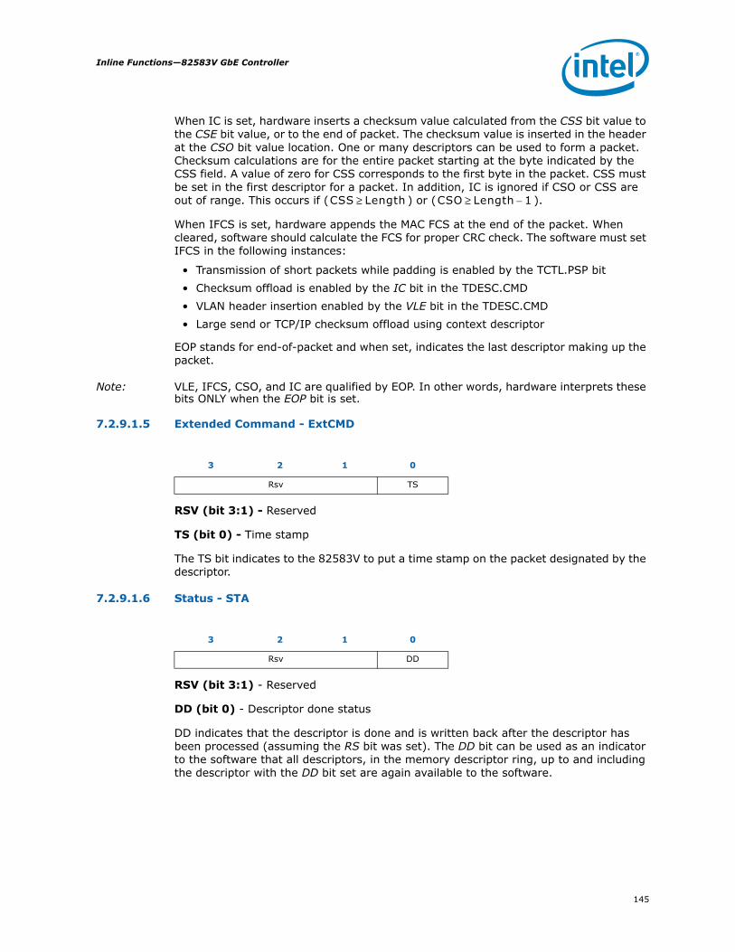
145
Inline Functions—82583V GbE Controller
When IC is set, hardware inserts a checksum value calculated from the CSS bit value to the CSE bit value, or to the end of packet. The checksum value is inserted in the header at the CSO bit value location. One or many descriptors can be used to form a packet. Checksum calculations are for the entire packet starting at the byte indicated by the CSS field. A value of zero for CSS corresponds to the first byte in the packet. CSS must be set in the first descriptor for a packet. In addition, IC is ignored if CSO or CSS are out of range. This occurs if ( ) or ( ).
When IFCS is set, hardware appends the MAC FCS at the end of the packet. When cleared, software should calculate the FCS for proper CRC check. The software must set IFCS in the following instances:
• Transmission of short packets while padding is enabled by the TCTL.PSP bit• Checksum offload is enabled by the IC bit in the TDESC.CMD• VLAN header insertion enabled by the VLE bit in the TDESC.CMD• Large send or TCP/IP checksum offload using context descriptor
EOP stands for end-of-packet and when set, indicates the last descriptor making up the packet.
Note: VLE, IFCS, CSO, and IC are qualified by EOP. In other words, hardware interprets these bits ONLY when the EOP bit is set.
7.2.9.1.5 Extended Command - ExtCMD
RSV (bit 3:1) - Reserved
TS (bit 0) - Time stamp
The TS bit indicates to the 82583V to put a time stamp on the packet designated by the descriptor.
7.2.9.1.6 Status - STA
RSV (bit 3:1) - Reserved
DD (bit 0) - Descriptor done status
DD indicates that the descriptor is done and is written back after the descriptor has been processed (assuming the RS bit was set). The DD bit can be used as an indicator to the software that all descriptors, in the memory descriptor ring, up to and including the descriptor with the DD bit set are again available to the software.
CSS Length≥ CSO Length 1–≥
3 2 1 0
Rsv TS
3 2 1 0
Rsv DD
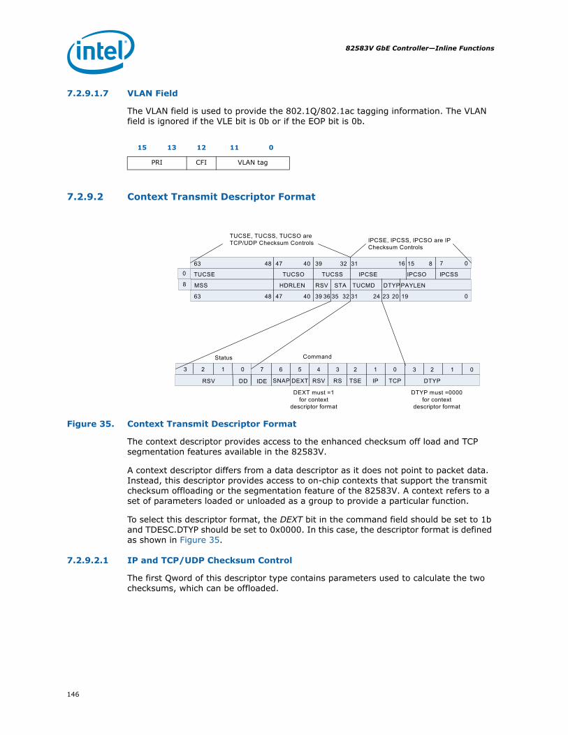
82583V GbE Controller—Inline Functions
146
7.2.9.1.7 VLAN Field
The VLAN field is used to provide the 802.1Q/802.1ac tagging information. The VLAN field is ignored if the VLE bit is 0b or if the EOP bit is 0b.
7.2.9.2 Context Transmit Descriptor Format
Figure 35. Context Transmit Descriptor Format
The context descriptor provides access to the enhanced checksum off load and TCP segmentation features available in the 82583V.
A context descriptor differs from a data descriptor as it does not point to packet data. Instead, this descriptor provides access to on-chip contexts that support the transmit checksum offloading or the segmentation feature of the 82583V. A context refers to a set of parameters loaded or unloaded as a group to provide a particular function.
To select this descriptor format, the DEXT bit in the command field should be set to 1b and TDESC.DTYP should be set to 0x0000. In this case, the descriptor format is defined as shown in Figure 35.
7.2.9.2.1 IP and TCP/UDP Checksum Control
The first Qword of this descriptor type contains parameters used to calculate the two checksums, which can be offloaded.
15 13 12 11 0
PRI CFI VLAN tag
078151631323940474863
PAYLENDTYPTUCMDSTAMSS
7 6 5 4 3 2 1 0
IDE SNAP DEXT RSV RS TSE IP TCP
8
Status
RSV DD
Command
3 2 1 0
IPCSSIPCSOIPCSETUCSSTUCSOTUCSE0
HDRLEN RSV
0192031323940474863 36 35 2324
TUCSE, TUCSS, TUCSO are TCP/UDP Checksum Controls IPCSE, IPCSS, IPCSO are IP
Checksum Controls
DEXT must =1 for context
descriptor format
3 2 1 0
DTYP
DTYP must =0000 for context
descriptor format
147
Inline Functions—82583V GbE Controller
IPCSS - IP Checksum Start - Specifies the byte offset from the start of the DMA'd data to the first byte to be included in the checksum. Setting this value to 0b means the first byte of the data would be included in the checksum. This field is limited to the first 256 bytes of the packet and must be less than or equal to the total length of a given packet. If this is not the case, the results are unpredictable.
IPCSO - IP Checksum Offset - Specifies where the resulting checksum should be placed. This field is limited to the first 256 bytes of the packet and must be less than or equal to the total length of a given packet. If this is not the case, the checksum is not inserted.
IPCSE - IP Checksum End - Specifies where the checksum should stop. A 16-bit value supports checksum off loading of packets as large as 64 KB. Setting the IPCSE field to all zeros means EOP. In this way, the length of the packet does not need to be calculated.
Note: When doing checksum or TCP segmentation with IPv6 headers IPCSE field should be set to 0x0000, IPCSS should be valid as in IPv4 packet and the IXSM bit in the data descriptor should be cleared.
Note: For proper IP checksum calculation, the IP Header Checksum field should be set to zero unless some adjustment is needed by the driver.
Similarly, TUCSS, TUCSO, TUCSE specify the same parameters for the TCP or UDP checksum.
Note: For proper TCP/UDP checksum calculation the TCP/UDP Checksum field should be set to the partial pseudo-header checksum value.
In case of 802.1Q header, the offset values depend on the VLAN insertion enable bit - CTRL.VME. When the CTRL.VME is not set (VLAN tagging included in the packet buffers), the offset values should include the VLAN tagging. When the CTRL.VME is set (VLAN tagging is taken from the packet descriptor), the offset values should exclude the VLAN tagging.
Note: When setting the TCP segmentation context, IPCSS and TUCSS are used to indicate the start of the IP and TCP headers respectively, and must be set even if checksum insertion is not desired.
In certain situations, software might need to calculate a partial checksum (the TCP pseudo-header for instance) to include bytes that are not contained within the range of start and end. If this is the case, this partial checksum should be placed in the packet data buffer, at the appropriate offset for the checksum. If no partial checksum is required, software must write a value of zero at this offset.
7.2.9.3 Max Segment Size - MSS
MSS controls the maximum segment size. This specifies the maximum TCP or UDP payload segment sent per frame, not including any header. The total length of each frame (or section) sent by the TCP segmentation mechanism (excluding 802.3ac tagging and Ethernet CRC) is MSS bytes + HRDLEN. The one exception is the last packet of a TCP segmentation that might be shorter. This field is ignored if TDESC.TSE is not set.

82583V GbE Controller—Inline Functions
148
7.2.9.3.1 Header Length - HDRLEN
HDRLEN is used to specify the length (in bytes) of the header to be used for each frame of a TCP segmentation operation. The first HDRLEN bytes fetched from data descriptor are stored internally and are used as a prototype header. The prototype header is updated for each packet and is prepended to the packet payload. For UDP packets this will normally be equal to UDP checksum offset + 2. For TCP messages it will normally be equal to TCP checksum offset + 4 + TCP header option bytes. This field is ignored if TDESC.TSE is not set.
Maximum limits for the HDRLEN and MSS fields are dictated by the lengths variables. However, there is a further restriction that for any TCP segmentation operation, the hardware must be capable of storing a complete framed fragment (completely-built frames) in the transmit FIFO prior to transmission. Therefore, the output TX FIFO (packet buffer) should at least have (MSS + HDRLEN) space available. In addition MSS must be set to a value more than 0x10 and HDRLEN must be smaller than 256 bytes.
7.2.9.4 Payload - PAYLEN
The Packet Length field (PAYLEN) is the total number of payload bytes for this TCP segmentation offload (for example, the total number of payload bytes includes those that are distributed across multiple frames after TCP segmentation is performed). Following the fetch of the prototype header, PAYLEN specifies the length of data that is fetched next from data descriptor. This field is also used to determine when last-frame processing needs to be performed. The PAYLEN specification does not include any header bytes. This field is ignored if TDESC.TSE is not set.
Note: There is no restriction on the overall PAYLEN specification with respect to the transmit FIFO size, once the MSS and HDRLEN specifications are legal.
7.2.9.5 Descriptor Type - DTYP
Setting the descriptor type (TDESC.DTYP) field to 0x0000 identifies this descriptor as a context descriptor.
7.2.9.6 Command - TUCMD
The command field (TDESC.TUCMD) provides options that control the checksum offloading and TCP segmentation features, along with some of the generic descriptor processing functions. Table 41 lists the bit definitions for the TDESC.TUCMD field. The IDE, DEXT, and RS bits are valid regardless of the state of TSE. All other bits are ignored if TSE=0b.
Table 41. Command TUCMD Fields
7 6 5 4 3 2 1 0
IDE SNAP DEXT Rsv RS TSE IP TCP

149
Inline Functions—82583V GbE Controller
IDE (bit 7) - Interrupt Delay Enable
SNAP (bit 6) - SNAP
DEXT (bit 5) - Descriptor extension (must be 1b for this descriptor type)
Rsv (bit 4) - Reserved
RS (bit 3) - Report status
TSE (bit 2) - TCP segmentation enable
IP (bit 1) - IP Packet type (IPv4=1b, IPv6=0b)
TCP (bit 0) - Packet type (TCP=1b,UDP=0b)
IDE activates a transmit interrupt delay timer. Hardware loads a countdown register when it writes back a transmit descriptor that has RS and IDE set. The value loaded comes from the IDV field of the Interrupt Delay (TIDV) register. When the count reaches zero, a transmit interrupt occurs if transmit descriptor write-back interrupts (TXDW) are enabled. Hardware always loads the transmit interrupt counter whenever it processes a descriptor with IDE set even if it is already counting down due to a previous descriptor. If hardware encounters a descriptor that has RS set, but not IDE, it generates an interrupt immediately after writing back the descriptor and clears the interrupt delay timer. Setting the IDE bit has no meaning without setting the RS bit.
Note: Although the transmit interrupt may be delayed, the descriptor write-back requested by setting the RS bit is performed without delay unless descriptor write-back bursting is enabled.
SNAP indicates that the TCP segmentation MAC header includes a SNAP header that needs to be updated by hardware.
The DEXT bit identifies this descriptor as one of the extended descriptor types and must be set to 1b.
When the RS bit is set, hardware writes back the DD bit once the DMA fetch completes.
Note: Descriptors with the null address (0), or zero length, transfer no data. If they have the RS bit in the command byte set, then the DD field in the status word is written when hardware processes them. Hardware only sets the DD bit for descriptors with RS set.
Note: Software can set the RS bit in each descriptor or, more likely, in specific descriptors such as the last descriptor of each packet.
TSE indicates that this descriptor is setting the TCP segmentation context. If this bit is zero, the descriptor defines a single packet TCP/UDP, IP checksum offload mode. When a descriptor of this type is processed, the device immediately updates the mode in question (TCP segmentation or checksum offloading) with values from the descriptor. This means that if any normal packets or TCP segmentation packets are in progress (a descriptor with EOP set has not been received for the given context) the results will likely be undesirable.
The IP bit is used to indicate what type of IP (IPv4 or IPv6) packet is used in the segmentation process. This is necessary for the 82583V to know where the IP Payload Length field is located. This does not override the checksum insertion bit, IXSM. The IP bit must only be set for IPv4 packets and cleared for IPv6 packets.
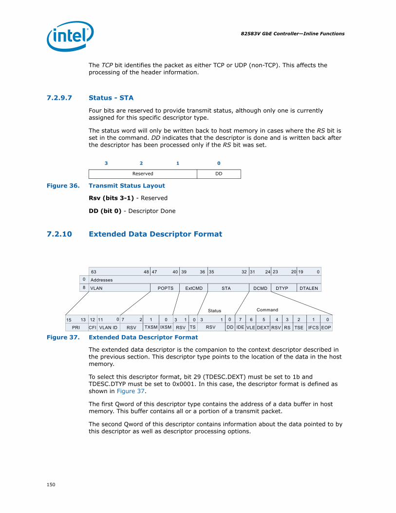
82583V GbE Controller—Inline Functions
150
The TCP bit identifies the packet as either TCP or UDP (non-TCP). This affects the processing of the header information.
7.2.9.7 Status - STA
Four bits are reserved to provide transmit status, although only one is currently assigned for this specific descriptor type.
The status word will only be written back to host memory in cases where the RS bit is set in the command. DD indicates that the descriptor is done and is written back after the descriptor has been processed only if the RS bit was set.
Figure 36. Transmit Status Layout
Rsv (bits 3-1) - Reserved
DD (bit 0) - Descriptor Done
7.2.10 Extended Data Descriptor Format
Figure 37. Extended Data Descriptor Format
The extended data descriptor is the companion to the context descriptor described in the previous section. This descriptor type points to the location of the data in the host memory.
To select this descriptor format, bit 29 (TDESC.DEXT) must be set to 1b and TDESC.DTYP must be set to 0x0001. In this case, the descriptor format is defined as shown in Figure 37.
The first Qword of this descriptor type contains the address of a data buffer in host memory. This buffer contains all or a portion of a transmit packet.
The second Qword of this descriptor contains information about the data pointed to by this descriptor as well as descriptor processing options.
3 2 1 0
Reserved DD
202331 2435 32363940474863
DTALENDTYPDCMDSTAVLAN
7 6 5 4 3 2 1 0
IDE VLE DEXT RSV RS TSE IFCS EOP
8
Status
DD
Command
3 1 003
Addresses0
POPTS ExtCMD
RSV
019
RSV
7 2 1 0
RSV TXSM IXSM
011
VLAN ID
12
CFI
1315
PRI
1
TS

151
Inline Functions—82583V GbE Controller
7.2.10.1 Data Length - DTALEN
The Data Length field (TDESC.DTALEN) is the total length of the data pointed to by this descriptor (the entire send), in bytes. For data descriptors not associated with a TCP segmentation operation (TDESC.TSE not set), the descriptor lengths are subject to the same restrictions specified for legacy descriptors (the sum of the lengths of the data descriptors comprising a single packet must be at least 80 bytes less than the allocated size of the transmit FIFO).
7.2.10.2 Descriptor Type - DTYP
Setting the descriptor type (TDESC.DTYP) field to 0x0001 identifies this descriptor as an extended data descriptor.
7.2.10.3 Command - DCMD
The command field (TDESC.DCMD) provides options that control the checksum offloading TCP segmentation features, along with some of the generic descriptor processing features. Table 42 lists the bit definitions for the DCMD field.
Table 42. Command DCMD Fields
IDE (bit 7) - Interrupt delay enable
VLE (bit 6) - VLAN enable
DEXT (bit 5) - Descriptor extension (must be 1b for this descriptor type)
RSV (bit 4) - Reserved
RS (bit 3) - Report status
TSE (bit 2) - TCP segmentation enable
IFCS (bit 1) - Insert FCS (also controls insertion of Ethernet CRC)
EOP (bit 0) - End of packet
IDE activates a transmit interrupt delay timer. Hardware loads a countdown register when it writes back a transmit descriptor that has RS and IDE set. The value loaded comes from the IDV field of the Interrupt Delay (TIDV) register. When the count reaches zero, a transmit interrupt occurs if transmit descriptor write-back interrupts (TXDW) are enabled. Hardware always loads the transmit interrupt counter whenever it processes a descriptor with IDE set even if it is already counting down due to a previous descriptor. If hardware encounters a descriptor that has RS set, but not IDE, it generates an interrupt immediately after writing back the descriptor and clears the interrupt delay timer. Setting the IDE bit has no meaning without setting the RS bit.
7 6 5 4 3 2 1 0
IDE VLE DEXT RSV RS TSE IFCS EOP

82583V GbE Controller—Inline Functions
152
Although the transmit interrupt might be delayed, the descriptor write-back requested by setting the RS bit is performed without delay unless descriptor write-back bursting is enabled.
VLE indicates that the packet is a VLAN packet (for example, that the hardware should add the VLAN Ether type and an 802.1Q VLAN tag to the TCP message).
Note: If the VLE bit is set to enable VLAN tag insertion, the CTRL.VME bit should also be set.
The DEXT bit identifies this descriptor as one of the extended descriptor types and must be set to 1b.
When the RS bit is set, the hardware writes back the DD bit once the DMA fetch completes.
Note: Descriptors with the null address (0), or zero length, transfer no data. If they have the RS bit in the command byte set, then the DD field in the status word is written when hardware processes them. Hardware only sets the DD bit for descriptors with RS set.
Software can set the RS bit in each descriptor or, more likely, in specific descriptors such as the last descriptor of each packet.
TSE indicates that this descriptor is part of the current TCP segmentation context. If this bit is not set, the descriptor is part of the normal non-segmentation context.
IFCS controls insertion of the Ethernet CRC. The packet FCS covers the TCP/IP headers. Therefore, when using the TCP segmentation offload, software must also use the FCS insertion.
Note: The VLE, IFCS, and VLAN fields are only valid in certain descriptors. If TSE is enabled, the VLE, IFCS, and VLAN fields are only valid in the first data descriptor of the TCP segmentation context. If TSE is not enabled, then these fields are only valid in the last descriptor of the given packet (qualified by the EOP bit).
EOP when set, indicates the last descriptor making up the packet.
Table 43. VLAN Tag Insertion Decision Table
VLE Action
0 Send generic Ethernet packet. IFCS controls insertion of FCS in normal Ethernet packets.
1Send 802.1Q packet; the Ethernet Type field comes from the VET register and the VLAN data comes from the special field of the TX descriptor; hardware always appends the FCS/CRC.

153
Inline Functions—82583V GbE Controller
7.2.10.4 Status - STA
The status field is written back to host memory in cases where the RS bit is set in the command field. The DD bit indicates that the descriptor is done after the descriptor has been processed.
Rsv (bit 3:1) - Reserved
DD (bit 0) - Descriptor done
7.2.10.5 Packet Options - POPTS
The POPTS field provides a number of options, which control the handling of this packet. This field is relevant only on the first data descriptor of a packet or segmentation context.
Rsv (bits 7:2) - Reserved
TXSM (bit 1) - Insert TCP/UDP checksum
IXSM (bit 0) - Insert IP checksum
IXSM and TXSM are used to control insertion of the IP and TCP/UDP checksums, respectively. If the corresponding bit is not set, whatever value software has placed into the checksum field of the packet data is placed on the wire.
Note: For proper values of the IP and TCP checksum, software must set the IXSM and TXSM when using the transmit segmentation.
Note: Software should not set this field for IPv6 packets.
7.2.10.6 VLAN
The VLAN field is used to provide the 802.1Q tagging information. The special field is ignored if the VLE bit in the DCMD command byte is 0b.
3 2 1 0
Rsv DD
7 2 1 0
Rsv TXSM IXSM
15 13 12 11 0
PRI CFI VLAN ID

82583V GbE Controller—Inline Functions
154
7.3 TCP SegmentationTCP segmentation is an offloading option of the TCP/IP stack. This is often referred to as Transmit Segmentation Offloading (TSO). This feature obligates the software device driver and hardware to carve up TCP messages, larger than the Maximum Transmission Unit (MTU) of the medium, into MSS sized frames that have appropriate layer 2, 3 (IP), and 4 (TCP) headers. These headers must have the correct sequence number, IP identification, checksum fields, options and flag values as required. This is done by breaking up the data into segments smaller than or equal to the MSS.
Note: Note that some of these values (such as the checksum values) are unique for each packet of the TCP message, and other fields such as the source IP address are constant for all frames associated with the TCP message.
The offloading of these mechanisms to the software device driver and the 82583V saves significant CPU cycles. The software device driver shares the additional tasks to support these options with the 82583V.
7.3.1 TCP Segmentation Performance Advantages
Performance advantages for a hardware implementation of TCP segmentation offload include:
• The stack does not need to partition the block to fit the MTU size, saving CPU cycles.
• The stack only computes one Ethernet, IP, and TCP header per segment (entire packet), saving CPU cycles.
• The stack interfaces with the software device driver only once per block transfer, instead of once per frame.
• Interrupts are easily reduced to once per TCP message instead of once per frame.• Fewer I/O accesses are required to command the the 82583V.
Note: TCP segmentation requires the transmit context descriptor format and the transmit data descriptor format.
7.3.2 Ethernet Packet Format
A TCP message can be fragmented across multiple pages in host memory. The 82583V partitions the data packet into standard Ethernet frames prior to transmission. The 82583V supports calculating the Ethernet, IP, TCP, and UDP headers, including checksum, on a frame-by-frame basis.
Figure 38. TCP/IP Packet Format
L2 L3 L4
Ethernet IP TCP DATA FCS

155
Inline Functions—82583V GbE Controller
Frame formats supported by the 82583V include:
• Ethernet 802.3• IEEE 802.1q VLAN (Ethernet 802.3ac) • Ethernet Type 2• Ethernet SNAP• IPv4 headers with options • IPv6 headers with IP option next headers• TCP with options• UDP with options
VLAN tag insertion is handled by hardware.
Note: IP tunneled packets are not supported for TSO operation.
Once the TCP segmentation context has been set, the next descriptor provides the initial data to transfer. This first descriptor(s must point to a packet of the type indicated. Furthermore, the data it points to might need to be modified by software as it serves as the prototype (partial pseudo-header) header for all packets within the TCP segmentation context. The following sections describe the supported packet types and the various updates which are performed by hardware. This should be used as a guide to determine what must be modified in the original packet header to make it a suitable prototype (partial pseudo-header) header.
7.3.3 TCP Segmentation Data Descriptors
The TCP segmentation data descriptor is the companion to the TCP segmentation context descriptor described in the previous section. For a complete description of the descriptor please refer to section 7.2.10.
To select this descriptor format, bit 29 (TDESC.DEXT) must be set to 1b and TDESC.DTYP must be set to 0x0001.
82583V GbE Controller—Inline Functions
156
7.3.4 TCP Segmentation Source Data
Once the TCP segmentation context has been set, the next descriptor (data descriptor) provides the initial data to transfer. This first data descriptor must point to data containing an Ethernet header of the type indicated. The 82583V fetches the prototype (partial pseudo-header) header from the host data buffer into an internal buffer and this header is prepended to every packet for this TSO operation. The prototype (partial pseudo-header) header is modified accordingly for each MSS sized segment. The following sections describe the supported packet types and the various updates that are performed by hardware. This should be used as a guide to determine what must be modified in the original packet header to make it a suitable prototype (partial pseudo-header) header.
The following summarizes the fields considered by the driver for modification in constructing the prototype (partial pseudo-header) header.
MAC Header (for SNAP)• MAC Header LEN field should be set to 0b.
IPv4 Header• Length should be set to zero.• Identification field should be set as appropriate for first packet of send (if not
already).• Header checksum should be zeroed out unless some adjustment is needed by the
software device driver.
IPv6 Header• Length should be set to zero.
TCP Header• Sequence number should be set as appropriate for first packet of send (if not
already).• PSH, and FIN flags should be set as appropriate for LAST packet of send.• TCP checksum should be set to the partial pseudo-header checksum.
UDP Header• UDP checksum should be set to the partial pseudo-header checksum.
The 82583V's DMA function fetches the IP, and TCP/UDP prototype (partial pseudo-header) header information from the initial descriptor and save them on-chip for individual packet header generation.
7.3.5 Hardware Performed Updating for Each Frame
The following sections describe the updating process performed by the hardware for each frame sent using the TCP segmentation capability.

157
Inline Functions—82583V GbE Controller
7.3.6 TCP Segmentation Use of Multiple Data Descriptors
TCP segmentation enables a series of data descriptors, each referencing a single physical address page, to reference a large packet contained in a single virtual-address buffer.
The only requirement on use of multiple data descriptors for TCP segmentation is as follows:
• If multiple data descriptors are used to describe the IP/TCP/UDP header section, each descriptor must describe one or more complete headers; descriptors referencing only parts of headers are not supported.
Note: It is recommended that the entire header section, as described by the TCP Context Descriptor HDRLEN field, be coalesced into a single buffer and described using a single data descriptor. If all the layer headers (L2-L4) are not coalesced into a single buffer, each buffer must not cross a 4 KB boundary, or be bigger than MAX_READ_REQUEST.
7.3.6.1 Transmit Checksum Offloading with TCP Segmentation
The 82583V supports checksum offloading as a component of the TCP segmentation offload feature and as a standalone capability.
The 82583V supports IP and TCP/UDP header options in the checksum computation for packets that are derived from the TCP segmentation feature.
Note: The 82583V is capable of computing one level of IP header checksum and one TCP/UDP header and payload checksum. In case of multiple IP headers, the software device driver has to compute all but one IP header checksum. The 82583V calculates checksums on the fly on a frame-by-frame basis and inserts the result in the IP/TCP/UDP headers of each frame. TCP and UDP checksum are a result of performing the checksum on all bytes of the payload and the pseudo header.
Three specific types of checksum are supported by the hardware in the context of the TCP Segmentation off load feature:
• IPv4 checksum (IPv6 does not have a checksum)• TCP checksum• UDP checksum
Each packet that is sent via the TCP segmentation offload feature optionally includes the IPv4 checksum and either the TCP or UDP checksum.
All checksum calculations use a 16-bit wide ones complement checksum. The checksum word is calculated on the outgoing data. The checksum field is written with the 16-bit ones complement sum of all 16-bit words in the range of CSS to CSE, including the checksum field itself.

82583V GbE Controller—Inline Functions
158
7.3.6.2 IP/TCP/UDP Header Updating
IP/TCP/UDP header is updated for each outgoing frame based on the IP/TCP header prototype (partial pseudo-header) which the hardware gets from the first descriptor and stores on chip. The IP/TCP/UDP headers are fetched from host memory into an on-chip 240 byte header buffer once for each TCP segmentation context (for performance reasons, this header is not fetched for each additional packet that will be derived from the TCP segmentation process). The checksum fields and other header information are updated on a frame-by-frame basis. The updating process is performed concurrently with the packet data fetch.
7.3.6.2.1 TCP/IP/UDP Header for the First Frame
The hardware makes the following changes to the headers of the first packet that is derived from each TCP segmentation context.
MAC Header (for SNAP)• Type/Len field = MSS + HDRLEN - 14
IPv4 Header• IP Total Length = MSS + HDRLEN - IPCSS• IP Checksum
IPv6 Header• Payload Length = MSS + HDRLEN - IPCSS - Ipv6Size (while Ipv6Size = 40Bytes)
TCP Header• Sequence Number: The value is the Sequence Number of the first TCP byte in this
frame.• If FIN flag = 1b, it is cleared in the first frame.• If PSH flag =1b, it is cleared in the first frame.• TCP Checksum
UDP Header• UDP length: MSS + HDRLEN - TUCSS • UDP Checksum
7.3.6.2.2 TCP/IP/UDP Header for the Subsequent Frames
The hardware makes the following changes to the headers of the subsequent packets that is derived from each TCP segmentation context.
Note: Number of bytes left for transmission = PAYLEN - (N * MSS). Where N is the number of frames that have been transmitted.
MAC Header (for SNAP Packets)• Type/Len field = MSS + HDRLEN - 14

159
Inline Functions—82583V GbE Controller
IPv4 Header• IP Identification: incremented from last value (wrap around)• IP Total Length = MSS + HDRLEN - IPCSS• IP Checksum
IPv6 Header• Payload Length = MSS + HDRLEN - IPCSS - Ipv6Size (while Ipv6Size = 40Bytes)
TCP Header• Sequence Number update: Add previous TCP payload size to the previous sequence
number value. This is equivalent to adding the MSS to the previous sequence number.
• If FIN flag = 1b, it is cleared in these frames.• If PSH flag =1b, it is cleared in these frames.• TCP Checksum
UDP Header• UDP Length: MSS + HDRLEN - TUCSS• UDP Checksum
7.3.6.2.3 TCP/IP/UDP Header for the Last Frame
The hardware makes the following changes to the headers of the last packet that is derived from each TCP segmentation context.
Note: Last frame payload bytes = PAYLEN - (N * MSS)
MAC Header (for SNAP Packets)• Type/Len field = Last frame payload bytes + HDRLEN - 14
IPv4 Header• IP Total Length = (last frame payload bytes + HDRLEN) - IPCSS• IP Identification: incremented from last value (wrap around)• IP Checksum
IPv6 Header• Payload Length = last frame payload bytes + HDRLEN - IPCSS - Ipv6Size (while
Ipv6Size = 40Bytes)
TCP Header• Sequence Number update: Add previous TCP payload size to the previous sequence
number value. This is equivalent to adding the MSS to the previous sequence number.
• If FIN flag = 1b, set it in this last frame• If PSH flag =1b, set it in this last frame• TCP Checksum

82583V GbE Controller—Inline Functions
160
UDP Header• UDP length: (last frame payload bytes + HDRLEN) - TUCSS• UDP Checksum
7.4 InterruptsThe 82583V supports the following interrupt modes:
• PCI legacy interrupts • PCI MSI - Message Signaled Interrupts
7.4.1 Legacy and MSI Interrupt Modes
In legacy and MSI modes, an interrupt cause is reflected by setting one of the bits in the ICR register, where each bit reflects one or more causes. This description of ICR register provides the mapping of interrupt causes (for example, a specific Rx queue event or a LSC event) to bits in the ICR.
Mapping of causes relating to the Tx and Rx queues as well as non-queue causes in this mode is not configurable. Each possible queue interrupt cause (such as the Rx queue, Tx queue or any other interrupt source) has an entry in the ICR.
The following configuration and parameters are involved:
• The ICR[31:0] bits are allocated to specific interrupt causes
7.4.2 Registers
The interrupt logic consists of the registers listed in the following table, plus the registers associated with MSI signaling.
Interrupt Cause Registers (ICR)
This register records the interrupts causes to provide to the software information on the interrupt source.
Register Acronym Function
Interrupt Cause ICR Records all interrupt causes - an interrupt is signaled when unmasked bits in this register are set.
Interrupt Cause Set ICS Enables software to set bits in the Interrupt Cause register.
Interrupt Mask Set/Read IMS Sets or reads bits in the interrupt mask.
Interrupt Mask Clear IMC Clears bits in the Interrupt mask.
Interrupt Auto Clear EIAC Enables bits in the ICR and IMS without a read or write of the ICR.
Interrupt Auto Mask IAM Enables bits in the IMS to be set automatically.

161
Inline Functions—82583V GbE Controller
The interrupt causes include:
• The receive and transmit related interrupts.• Other bits in this register are the legacy indication of interrupts as the MDIC
completes a link status change. There is a specific Other Cause bit that is set if one of these bits are set.
Interrupt Cause Set Register (ICS)
This registers allows triggering an immediate interrupt by software, By writing 1b to bits in ICS the corresponding bits in ICR is set Used usually to rearm interrupts the software didn't have time to handle in the current interrupt routine.
Interrupt Mask Set and Read Register (IMS) and Interrupt Mask Clear Register (IMC)
Interrupts appear on PCIe only if the interrupt cause bit is a one and the corresponding interrupt mask bit is a one. Software blocks assertion of an interrupt by clearing the corresponding bit in the mask register. The cause bit stores the interrupt event regardless of the state of the mask bit. Clear and set make this register more thread safe by avoiding a read-modify-write operation on the mask register. The mask bit is set for each bit written to a one in the set register and cleared for each bit written in the clear register. Reading the set register (IMS) returns the current mask register value.
Interrupt Auto Clear Enable Register (EIAC)
Bits 24:20 in this register enables clearing of the corresponding bit in ICR following interrupt generation. When a bit is set, the corresponding bit in ICR and in IMS is automatically cleared following an interrupt.
Bits in the ICR that are not set in EIAC need to be cleared with ICR read or ICR write-to-clear.
Interrupt Auto Mask Enable register (IAM)
Each bit in this register enables setting of the corresponding bit in IMS following write to-clear to ICR.
7.4.3 Interrupt Moderation
The 82583V implements interrupt moderation to reduce the number of interrupts software processes. The moderation scheme is based on a timer called ITR Interrupt Throttle register). In general terms, the ITR defines an interrupt rate by defining the time interval between consecutive interrupts.
The number of ITR registers is:
• A single ITR is used (ITR).
Software uses ITR to limit the rate of delivery of interrupts to the host CPU. It provides a guaranteed inter-interrupt delay between interrupts asserted by the network controller, regardless of network traffic conditions.
82583V GbE Controller—Inline Functions
162
The following algorithm converts the inter-interrupt interval value to the common 'interrupts/sec' performance metric:
Interrupts/sec = (256 * 10-9 sec x interval) -1
For example, if the interval is programmed to 500d, the 82583V guarantees the CPU is not interrupted by it for at least 128 μs from the last interrupt.
Inversely, inter-interrupt interval value can be calculated as:
Inter-interrupt interval = (256 * 10-9 sec x interrupts/sec) -1
The optimal performance setting for this register is very system and configuration specific.
ITR rules:
• The maximum observable interrupt rate from the adapter should not exceed 7813 interrupts/sec.
• The Extended Interrupt Throttle register should default to 0x0 upon initialization and reset.
Each time an interrupt event happens, the corresponding bit in the ICR is activated. The interrupt flow should follow the following diagram:

163
Inline Functions—82583V GbE Controller
Figure 39. Interrupt Throttle Flow Diagram
For cases where the 82583V is connected to a small number of clients, it is desirable to fire off the interrupt as soon as possible with minimum latency.
Start count down
vAssert Interrupt
Counter = 0?
Load counter with interval
Yes
Yes
Interrupt active
?
Yes
No
Intr ack ?
No
No
vClear Interrupt
Yes

82583V GbE Controller—Inline Functions
164
Case A: Heavy load, interrupts moderated
Case B: Light load, interrupts immediately on packet receive
7.4.4 Clearing Interrupt Causes
The 82583V has two methods available for to clear ICR bits: clear-on-write and clear-on-read.
Pkt Pkt Pkt Pkt Pkt Pkt
ITR delay ITR delay
Intr Intr Intr
Pkt Pkt
Pkt Pkt
ITR delay
Intr Intr

165
Inline Functions—82583V GbE Controller
Write to Clear
The ICR register clears specific interrupt cause bits in the register after writing 1b to those bits. Any bit that was written with a 0b remains unchanged.
Read to clear
All bits in the ICR register are cleared on a read to ICR.
7.5 802.1q VLAN SupportThe 82583V provides several specific mechanisms to support 802.1q VLANs:
• Optional adding (for transmits) and ping (for receives) of IEEE 802.1q VLAN tags.• Optional ability to filter packets belonging to certain 802.1q VLANs.
7.5.1 802.1q VLAN Packet Format
The following diagram compares an untagged 802.3 Ethernet packet with an 802.1q VLAN tagged packet:
Note: The CRC for the 802.1q tagged frame is re-computed, so that it covers the entire tagged frame including the 802.1q tag header. Also, maximum frame size for an 802.1q VLAN packet is 1522 octets as opposed to 1518 octets for a normal 802.3z Ethernet packet.
7.5.1.1 802.1q Tagged Frames
For 802.1q, the Tag Header field consists of four octets comprised of the Tag Protocol Identifier (TPID) and Tag Control Information (TCI); each taking two octets. The first 16 bits of the tag header makes up the TPID. It contains the protocol type, which identifies the packet as a valid 802.1q tagged packet.
The two octets making up the TCI contain three fields:
• User Priority (UP)• Canonical Form Indicator (CFI). Should be 0b for transmits. For receives, the
device has the capability to filter out packets that have this bit set. See the CFIEN and CFI bits in the RCTL described in section 9.2.5.1.
• VLAN Identifier (VID)
802.3 Packet #Octets 802.1q VLAN Packet #Octets
DA 6 DA 6
SA 6 SA 6
Type/Length 2 802.1q Tag 4
Data 46-1500 Type/Length 2
CRC 4 Data 46-1500
CRC* 4
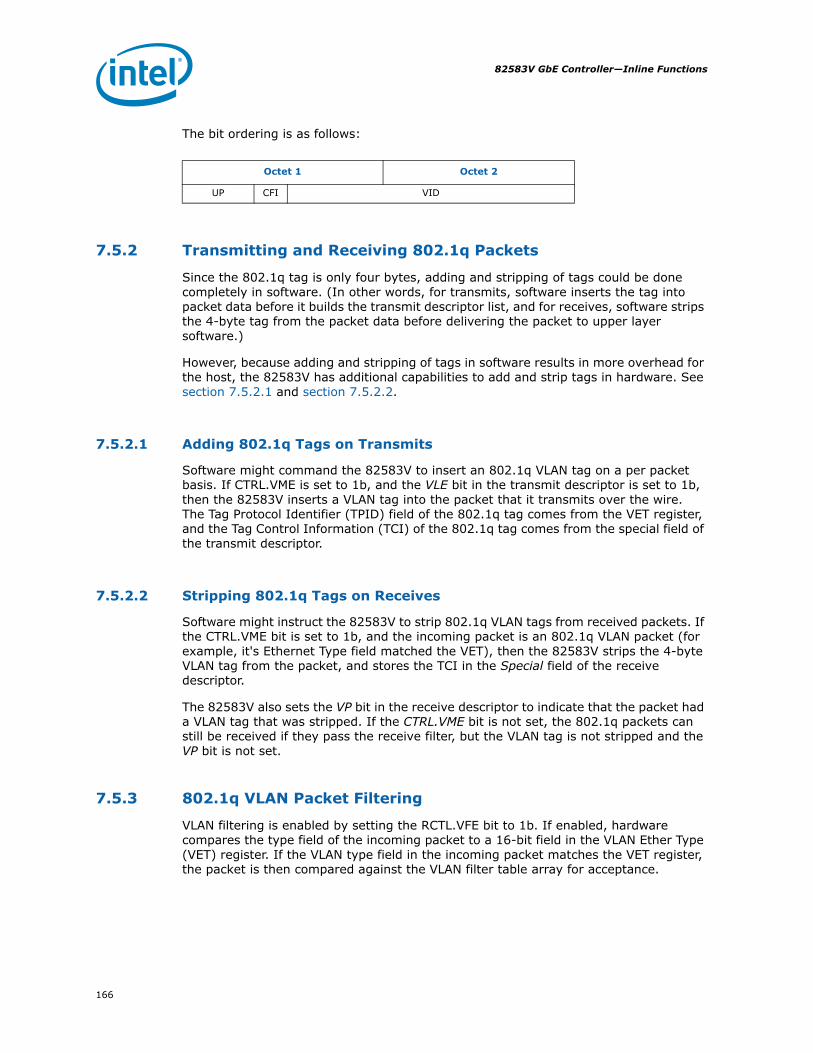
82583V GbE Controller—Inline Functions
166
The bit ordering is as follows:
7.5.2 Transmitting and Receiving 802.1q Packets
Since the 802.1q tag is only four bytes, adding and stripping of tags could be done completely in software. (In other words, for transmits, software inserts the tag into packet data before it builds the transmit descriptor list, and for receives, software strips the 4-byte tag from the packet data before delivering the packet to upper layer software.)
However, because adding and stripping of tags in software results in more overhead for the host, the 82583V has additional capabilities to add and strip tags in hardware. See section 7.5.2.1 and section 7.5.2.2.
7.5.2.1 Adding 802.1q Tags on Transmits
Software might command the 82583V to insert an 802.1q VLAN tag on a per packet basis. If CTRL.VME is set to 1b, and the VLE bit in the transmit descriptor is set to 1b, then the 82583V inserts a VLAN tag into the packet that it transmits over the wire. The Tag Protocol Identifier (TPID) field of the 802.1q tag comes from the VET register, and the Tag Control Information (TCI) of the 802.1q tag comes from the special field of the transmit descriptor.
7.5.2.2 Stripping 802.1q Tags on Receives
Software might instruct the 82583V to strip 802.1q VLAN tags from received packets. If the CTRL.VME bit is set to 1b, and the incoming packet is an 802.1q VLAN packet (for example, it's Ethernet Type field matched the VET), then the 82583V strips the 4-byte VLAN tag from the packet, and stores the TCI in the Special field of the receive descriptor.
The 82583V also sets the VP bit in the receive descriptor to indicate that the packet had a VLAN tag that was stripped. If the CTRL.VME bit is not set, the 802.1q packets can still be received if they pass the receive filter, but the VLAN tag is not stripped and the VP bit is not set.
7.5.3 802.1q VLAN Packet Filtering
VLAN filtering is enabled by setting the RCTL.VFE bit to 1b. If enabled, hardware compares the type field of the incoming packet to a 16-bit field in the VLAN Ether Type (VET) register. If the VLAN type field in the incoming packet matches the VET register, the packet is then compared against the VLAN filter table array for acceptance.
Octet 1 Octet 2
UP CFI VID

167
Inline Functions—82583V GbE Controller
The Virtual LAN ID field indexes a 4096 bit vector. If the indexed bit in the vector is one; there is a virtual LAN match. Software might set the entire bit vector to ones if the node does not implement 802.1q filtering. The register description of the VLAN filter table array is described in detail in section 9.2.5.20.
In summary, the 4096-bit vector is comprised of 128, 32-bit registers. Matching to this bit vector follows the same algorithm as indicated in section 7.1.1 for multicast address filtering. The VLAN Identifier (VID) field consists of 12 bits. The upper 7 bits of this field are decoded to determine the 32-bit register in the VLAN filter table array to address and the lower 5 bits determine which of the 32 bits in the register to evaluate for matching.
Two other bits in the Receive Control register (see section 9.2.5.1), CFIEN and CFI, are also used in conjunction with 802.1q VLAN filtering operations. CFIEN enables the comparison of the value of the CFI bit in the 802.1q packet to the Receive Control register CFI bit as acceptance criteria for the packet.
Note: The VFE bit does not effect whether the VLAN tag is stripped. It only affects whether the VLAN packet passes the receive filter.
Table 44 lists reception actions per control bit settings.
Table 44. Packet Reception Decision Table
Note: A packet is defined as a VLAN/802.1q packet if its type field matches the VET.
7.6 LEDs The 82583V implements three output drivers intended for driving external LED circuits per port. Each of the three LED outputs can be individually configured to select the particular event, state, or activity, which is indicated on that output. In addition, each LED can be individually configured for output polarity as well as for blinking versus non-blinking (steady-state) indication.
The configuration for LED outputs is specified via the LEDCTL register. Furthermore, the hardware-default configuration for all the LED outputs, can be specified via NVM fields, thereby supporting LED displays configurable to a particular OEM preference.
Is packet
802.1q?
CTRL.VME
RCTL.VFE Action
No X X Normal packet reception.
Yes 0b 0bReceive a VLAN packet if it passes the standard filters (only). Leave the packet as received in the data buffer. VP bit in receive descriptor is cleared.
Yes 0b 1b
Receive a VLAN packet if it passes the standard filters and the VLAN filter table. Leave the packet as received in the data buffer (for example, the VLAN tag would not be stripped). VP bit in receive descriptor is cleared.
Yes 1b 0bReceive a VLAN packet if it passes the standard filters (only). Strip off the VLAN information (four bytes) from the incoming packet and store in the descriptor. Sets the VP bit in receive descriptor.
Yes 1b 1b
Receive a VLAN packet if it passes the standard filters and the VLAN filter table. Strip off the VLAN information (four bytes) from the incoming packet and store in the descriptor. Sets the VP bit in receive descriptor.

82583V GbE Controller—Inline Functions
168
Each of the three LED's might be configured to use one of a variety of sources for output indication. The Mode bits control the LED source:
• LINK_100/1000 is asserted when link is established at either 100 or 1000 Mb/s.• LINK_10/1000 is asserted when link is established at either 10 or 1000 Mb/s.• LINK_UP is asserted when any speed link is established and maintained.• ACTIVITY is asserted when link is established and packets are being transmitted or
received.• LINK/ACTIVITY is asserted when link is established AND there is NO transmit or
receive activity• LINK_10 is asserted when a 10 Mb/s link is established and maintained.• LINK_100 is asserted when a 100 Mb/s link is established and maintained.• LINK_1000 is asserted when a 1000 Mb/s link is established and maintained.• FULL_DUPLEX is asserted when the link is configured for full duplex operation.• COLLISION is asserted when a collision is observed.• PAUSED is asserted when the device's transmitter is flow controlled.• LED_ON is always asserted; LED_OFF is always de-asserted.
The IVRT bits enable the LED source to be inverted before being output or observed by the blink-control logic. LED outputs are assumed to normally be connected to the negative side (cathode) of an external LED.
The BLINK bits control whether the LED should be blinked while the LED source is asserted, and the blinking frequency (either 200 ms on and 200 ms off or 83 ms on and 83 ms off)1. The blink control can be especially useful for ensuring that certain events, such as ACTIVITY indication, cause LED transitions, which are sufficiently visible to a human eye. The same blinking rate is shared by all LEDs.
Note: Note that the LINK/ACTIVITY source functions slightly different from the others when BLINK is enabled. The LED is off if there is no LINK, on if there is LINK and no ACTIVITY, and blinking if there is LINK and ACTIVITY.
1. While in Smart Power Down mode, the blinking durations are increased by 5x to 1 second and 415 ms, respectively.

169
Inline Functions—82583V GbE Controller
Note: This page intentionally left blank.

82583V GbE Controller—Power Management and Delivery
170
8.0 Power Management and Delivery
The 82583V supports the Advanced Configuration and Power Interface (ACPI 2.0) specification as well as Advanced Power Management (APM). This section describes how power management is implemented in the 82583V.
Implementation requirements were obtained from the following documents:
• PCI Bus Power Management Interface Specification .................................Rev 1.1• PCI Express Base Specification .............................................................Rev.1.1• ACPI Specification ...............................................................................Rev 2.0• PCI Express Card Electromechanical Specification ....................................Rev 1.1
8.1 AssumptionsThe following assumptions apply to the implementation of power management for the 82583V.
• The software device driver sets up the filters prior to the system transition of the 82583V to a D3 state.
• Prior to transition from D0 to the D3 state, the operating system ensures that the software device driver has been disabled. See Section 8.4.4.2.3 for the 82583V behavior on D3 entry.
• No wake up capability, except APM wake up if enabled in the NVM, is required after the system puts the 82583V in D3 state and then returns the 82583V to D0.
• If the APMPME bit in the Wake Up Control (WUC) register is 1b, it is permissible to assert PE_WAKE_N even when PME_En is 0b.
8.2 Power ConsumptionTable 16 and Table 17 list power consumption in various modes (see Section 3.5). The following sections describe the requirements in specific power states.

171
Power Management and Delivery—82583V GbE Controller
8.3 Power Delivery82583V operates from the following power rails:
• A 3.3 V dc power rail for internal power regulation and for periphery. The 3.3 V dc should be supplied by an external power source.
• A 1.9 V dc power rail.• A 1.05 V dc power rail.
8.3.1 The 1.9 V dc Rail
The 1.9 V dc rail is used for core and I/O functions. It also feeds internal regulators to a lower 1.05 V dc core voltage. The 1.9 V dc rail can be generated in one of two ways:
• An external power supply not dependent on support from the 82583V. For example, the platform designer might choose to route a platform-available 1.9 V dc supply to the 82583V.
• Internal voltage regulator solution, where the control logic for the power transistor is embedded in the 82583V, while the power transistor is placed externally. Control is done using the CTRL19 pin.
8.3.2 The 1.05 V dc Rail
The 1.05 V dc rail is used for core functions and can be generated in one of the following ways:
• An external power supply not dependent on support from the 82583V.• Internal voltage regulator solution, where the control logic for the power transistor
is embedded in the 82583V, while the power transistor is placed externally. Control is done using the CTRL10 pin.
• A complete internal voltage regulator solution. The internal voltage regulator can be disabled by the DIS_REG10 pin.
8.4 Power Management
8.4.1 82583V Power States
The 82583V supports D0 and D3 power states defined in the PCI Power Management and PCIe specifications. D0 is divided into two sub-states: D0u (D0 Un-initialized), and D0a (D0 active). In addition, the 82583V supports a Dr state that is entered when PE_RST_N is asserted (including the D3cold state).
Figure 40 shows the power states and transitions between them.

82583V GbE Controller—Power Management and Delivery
172
Figure 40. Power Management State Diagram
8.4.2 Auxiliary Power Usage
If ADVD3WUC=1b, the 82583V uses the AUX_PWR indication that auxiliary power is available to the controller, and therefore advertises D3cold wake up support. The amount of power required for the function (which includes the entire NIC) is advertised in the Power Management Data register, which is loaded from the NVM.
If D3cold is supported, the PME_En and PME_Status bits of the Power Management Control/Status Register (PMCSR), as well as their shadow bits in the Wake Up Control (WUC) register is reset only by the power up reset (detection of power rising).
The only effect of setting AUX_PWR to 1b is advertising D3cold wake up support and changing the reset function of PME_En and PME_Status. AUX_PWR is a strapping option in the 82583V.
The 82583V tracks the PME_En bit of the Power Management Control / Status Register (PMCSR) and the Auxiliary (AUX) Power PM Enable bit of the PCIe Device Control register to determine the power it might consume (and therefore its power state) in the D3cold state (internal Dr state).
Dr D0u
D0aD3
PE_RST_N de-assertion and EEPROM read
done
PE_RST_Nassertion
PE_RST_Nassertion
PE_RST_Nassertion
Write 11bto power
state
Write 00bto power
state
Enablemaster or
slave access
Internal PowerOn Reset assertion
Hot (in-band) Reset

173
Power Management and Delivery—82583V GbE Controller
The AUX Power PM Enable bit in the PCIe Device Control register determines if the 82583V complies with the auxiliary power regime defined in the PCIe specification. If set, the 82583V might consume higher power for any purpose (such as, even if PME_En is not set).
If the AUX Power PM Enable bit of the PCIe Device Control register is cleared, higher power consumption is determined by the PCI-PM legacy PME_En bit in the Power Management Control / Status Register (PMCSR).
Note: In the current implementation, the AUX Power PM Enable bit is hardwired to 0b.
8.4.3 Power Limits by Certain Form Factors
Table 45 lists the power limitations introduced by different form factors.
Table 45. Power Limits by Form Factor
1. This auxiliary current limit only applies when the primary 3.3 V dc voltage source is not available (such as, the NIC is in a low power D3 state.
2. The 82583V exceeds the allowed power consumption in GbE speed. It therefore cannot run from aux power, restricting the 82583V speed in Dr state.
The 82583V therefore implements two NVM bits to disable GbE operation in certain cases:
1. The Disable 1000 NVM bit disables 1000 Mb/s operation under all conditions.2. The Disable 1000 in non-D0a CSR bit disables 1000 Mb/s operation in non-D0a
states. If Disable 1000 in non-D0a is set, and the 82583V is at GbE speed on entry to a non-D0a state, then the device removes advertisement for 1000 Mb/s and auto-negotiates. The Disable 1000 in non-D0a bit is loaded from the NVM.
Note: The 82583V restarts link auto-negotiation each time it transitions from a state where GbE speed is enabled to a state where GbE speed is disabled, or vice versa. For example, if Disable 1000 in non-D0a is set but Disable 1000 is clear, the 82583V restarts link auto-negotiation on transition from D0 state to D3 or Dr states.
8.4.4 Power States
8.4.4.1 D0 Uninitialized State
The D0u state is a low-power state used after PE_RST_N is de-asserted following a power up (cold or warm), on hot reset (in-band reset through a PCIe physical layer message), or on D3 exit.
Form Factor
LOM PCIe NIC (x1 connector)
Main 3 A @ 3.3 V dc 3 A @ 3.3 V dc
Auxiliary (aux enabled) 375 mA @ 3.3 V dc 375 mA @ 3.3 V dc
Auxiliary (aux disabled) 20 mA @ 3.3 V dc

82583V GbE Controller—Power Management and Delivery
174
When entering the D0u state, the 82583V disables all wake ups and asserts a reset to the PHY while the NVM is being read. If the APM Mode bit in the NVM's Initialization Control Word 2 is set, then APM wake up is enabled.
8.4.4.1.1 Entry into D0u state
D0u is reached from either the Dr state (on assertion of Internal PwrGd) or the D3hot state (by configuration software writing a value of 00b to the Power State field of the PCI-PM registers).
Asserting Internal PwrGd means that the entire state of the device is cleared, other than sticky bits. The state is loaded from the NVM, followed by establishment of the PCIe link. Once this is done, configuration software can access the device.
On a transition from the D3 to D0u state, the 82583V’s PCI configuration space is not reset. Per the PCI Power Management Specification (revision 1.1, Section 5.4), software “will need to perform a full re-initialization of the function including its PCI Configuration Space.”
8.4.4.2 D0active State
Once memory space is enabled, all internal clocks are activated and the 82583V enters an active state. It can transmit and receive packets if properly configured by the software device driver. The PHY is enabled or re-enabled by the software device driver to operate / auto-negotiate to full-line speed/power if not already operating at full capability. Any APM Wakeup previously active remains active. The software device driver can deactivate APM Wakeup by writing to the WUC register, or activate other wake-up filters by writing to the Wake Up Filter Control (WUFC) register.
Note: Fields that are auto-loaded from the NVM, like WUC.APME, should be configured through an NVM setting, because D3 to D0 power state transition causes NVM auto-read to reload those bits from the NVM.
8.4.4.2.1 Entry to D0a State
D0a is entered from the D0u state by writing a 1b to the Memory Access Enable or the I/O Access Enable bit in the PCI Command register. The DMA, MAC, and PHY are enabled.
8.4.4.2.2 D3 State (=PCI-PM D3hot)
When the system writes a 11b to the Power State field in the PMCSR, the 82583V transitions to D3. Any wake-up filter settings that were enabled before entering this reset state are maintained. Upon transition to D3 state, the 82583V clears the Memory Access Enable and I/O Access Enable bits of the PCI Command register, which disables memory access decode. In D3, the 82583V only responds to PCI configuration accesses and does not generate master cycles.
A D3 state is followed by either a D0u state (in preparation for a D0a state) or by a transition to Dr state (PCI-PM D3cold state). To transition back to D0u, the system writes a 00b to the Power State field of the PMCSR. Transition to Dr state is through PE_RST_N assertion.

175
Power Management and Delivery—82583V GbE Controller
8.4.4.2.3 Entry to D3 State
Transition to the D3 state is through a configuration write to the Power State field of the PCI-PM registers.
Prior to transition from D0 to the D3 state, the software device driver disables scheduling of further tasks to the 82583V, as follows:
• It masks all interrupts• It does not write to the Transmit Descriptor Tail (TDT) register• It does not write to the Receive Descriptor Tail (RDT) register• Operates the master disable algorithm as defined in Section 6.1.3.10.
If wake-up capability is needed, the software device driver should set up the appropriate wake-up registers and the system should write a 1b to the PME_En bit in the PMCSR or to the AUX Power PM Enable bit of the PCIe Device Control register prior to the transition to D3.
As a response to being programmed into the D3 state, the 82583V brings its PCIe link into the L1 link state. As part of the transition into L1 state, the 82583V suspends scheduling of new Transaction Layer Protocols (TLPs) and waits for the completion of all previous TLPs it has sent. The 82583V clears the Memory Access Enable and I/O Access Enable bits of the PCI Command register, which disables memory access decode. Any receive packets that have not been transferred into system memory are kept in the device (and discarded later on D3 exit). Any transmit packets that were not sent, can still be transmitted (assuming the Ethernet link is up).
To reduce power consumption, if APM wake and PCI-PM PME are enabled, the PHY auto-negotiates to a lower link speed on D3 entry (see Section 8.4.4.2.3).

82583V GbE Controller—Power Management and Delivery
176
8.4.4.3 Dr State
Transition to Dr state is initiated on three occasions:
• At system power up - Dr state begins with the assertion of the internal power detection circuit (Internal Power On Reset) and ends with the assertion of the Internal Pwrgd signal (indicating that the system de-asserted its PCIe PE_RST_N signal).
• At transition from a D0a state - During operation, the system might assert PCIe PE_RST_N at any time. In an ACPI system, a system transition to the G2/S5 state causes a transition from D0a to Dr state.
• At transition from a D3 state - The system transitions the device into the Dr state by asserting PCIe PE_RST_N.
The 82583V meets the restrictions on using auxiliary power, defined in the PCI-PM specification:
1. If wake is enabled (either APM wake or ACPI wake), then the 82583V might consume up to 375 mA @ 3.3 V dc.
2. If wake is disabled, then the 82583V might consume up to 20 mA @ 3.3 V dc.
The restrictions apply to all cases of Dr state (power up, D3 entry, Dr entry from D0).
Note: When the wake configuration is unknown (for example, during power up before an NVM read), the 82583V must meet the 20 mA limit.
The system might maintain PE_RST_N asserted for an arbitrary time. The de-assertion (rising edge) of PE_RST_N causes a transition to D0u state.
Any Wake-up filter settings that were enabled before entering this reset state are maintained.
8.4.4.3.1 Entry to Dr State
Dr entry on platform power up begins by asserting the internal power detection circuit (Internal Power On Reset). The NVM is read and determines device configuration. If the APM Enable bit in the NVM's Initialization Control Word 2 is set, then APM wake up is enabled. The PHY and MAC states are determined by the state of APM wake. To reduce power consumption, if APM wake is enabled, the PHY auto-negotiates to a lower link speed on Dr entry (see Section 8.4.4.3.1). The PCIe link is not enabled in Dr state following system power up (since PERS# is asserted).
Entry to Dr state from D0a state is by asserting the PE_RST_N signal. An ACPI transition to the G2/S5 state is reflected in a device transition from D0a to Dr state. The transition might be orderly (for example, the designer selected the shut down option), in which case the software device driver might have a chance to intervene. Or, it might be an emergency transition (such as, power button override), in which case, the software device driver is not notified.
To reduce power consumption, if APM wake or PCI-PM PME is enabled, the PHY auto-negotiates to a lower link speed on D0a to Dr transition (see Section 8.4.4.3.1).
Transition from D3 state to Dr state is done by asserting the PE_RST_N signal. Prior to that, the system initiates a transition of the PCIe link from the L1 state to either the L2 or L3 state. The link enters L2 state if PCI-PM PME is enabled.

177
Power Management and Delivery—82583V GbE Controller
8.4.4.4 Device Disable
For a LOM design, it might be desirable for the system to provide BIOS-setup capability for selectively enabling or disabling LOM devices. This might allow the designers more control over system resource-management, avoid conflicts with add-in NIC solutions, etc. The 82583V provides support for selectively enabling or disabling it.
• Device Disable - the device is in a global power down state.
Device disable is initiated by asserting the asynchronous DEV_OFF_N pin. The DEV_OFF_N pin has an internal pull-up resistor, so that it can be left not connected to enable device operation.
While in device disable mode, the PCIe link is in L3 state. The PHY is in power-down mode. All internal clocks are gated. Output buffers are tri-stated.
Asserting or de-asserting PCIe PE_RST_N does not have any effect while the device is in device disable mode (for example, the device stays in the respective mode as long as DEV_OFF_N is asserted). However, the device might momentarily exit the device disable mode from the time PCIe PE_RST_N is de-asserted again and until the NVM is read.
Note: Note to system designers: The DEV_OFF_N pin should maintain its state during system reset and system sleep states. It should also insure the proper default value on system power up. For example, a system designer could use a GPIO pin that defaults to 1b (enable) and is on system suspend power (for example, it maintains state in S0-S5 ACPI states).
8.4.4.5 Link-Disconnect
In any of D0u, D0a, D3, or Dr states, the 82583V enters a link-disconnect state if it detects a link-disconnect condition on the Ethernet link. Note that the link-disconnect state is invisible to software (other than the Link Energy Detect bit state). In particular, while in D0 state, software might be able to access any of the device registers as in a link-connect state.
During link disconnect mode, the CCM PLL might be shut down. See Section 8.4.4.5.
8.4.5 Timing of Power-State Transitions
The following sections give detailed timing for the state transitions. In the diagrams the dotted connecting lines represent the 82583V requirements, while the solid connecting lines represent the 82583V guarantees.
The timing diagrams are not to scale. The clocks edges are shown to indicate running clocks only, they are not used to indicate the actual number of cycles for any operation.
8.4.5.1 Transition From D0a to D3 and Back Without PE_RST_N
Figure 41 shows the 82583V’s reaction to a D3 transition.

82583V GbE Controller—Power Management and Delivery
178
Figure 41. D3hot Transition Timing Diagram
Table 46. Notes to D3hot Timing Diagram
8.4.5.2 Transition From D0a to D3 and Back with PE_RST_N
Figure 42 shows the 82583V’s reaction to a D3 transition.
PCIe Reference Clock
PCIe PwrGd
PHY Reset
PCIe Link
Reading EEPROM Auto Read
DState D3 D0u D0
Wake Up Enabled
Memory Access Enable
L0
D3 write
APMAny mode
D0 Write
D0a
2
L1 L0
PHY Power State full fullpower-managed power-managed
tee
1
3
4
5
6
7
td0mem
Ext. Conf.
Note Description
1 Writing 11b to the Power State field of the PMCSR transitions the 82583V to D3.
2 The system keeps the 82583V in D3 state for an arbitrary amount of time.
3 To exit D3 state the system writes 00b to the Power State field of the PMCSR.
4 APM wake up mode can be enabled based on what is read in the NVM.
5 After reading the NVM, reset to the PHY is de-asserted. The PHY operates at reduced-speed if APM wake up is enabled, else powered-down.
6 The system can delay an arbitrary time before enabling memory access.
7Writing a 1b to the Memory Access Enable bit or to the I/O Access Enable bit in the PCI Command register transitions the 82583V from D0u to D0 state and returns the PHY to full-power/speed operation.

179
Power Management and Delivery—82583V GbE Controller
Figure 42. D3cold Transition Timing Diagram
Table 47. Notes to D3cold Timing Diagram
PCIe Reference Clock
PCIe PwrGd
DState
PHY Power State
D0u
Reading EEPROM Auto Read
D0a
power-managed full
Reset to PHY(active low)
PCIe Link
Wake Up Enabled
Dr
11
Any mode APM
full
D3 write
D0a D3
15
L0 L1 L2/L3 L01
2
6
13 14
3
4a
4b
12
Internal PCIe clock (2.5 GHz)
Internal PwrGd (PLL) 9
7
8
10
tee
tppg-clkint
tpgtrntpgrestpgcfg
tclkpr
tpgdl
tl2clktclkp
gtPWRGD-CLK
tl2pg
5
L0
Ext.Conf.
Note Description
1 Writing 11b to the Power State field of the PMCSR transitions the 82583V to D3. PCIe link transitions to L1 state.
2 The system can delay an arbitrary amount of time between setting D3 mode and transition the link to an L2 or L3 state.
3 Following link transition, PE_RST_N is asserted.
4 The system must assert PE_RST_N before stopping the PCIe reference clock. It must also wait tl2clk after link transition to L2/L3 before stopping the reference clock.
5 On assertion of PE_RST_N, the 82583V transitions to Dr state.
6 The system starts the PCIe reference clock tPWRGD-CLK before de-asserting PE_RST_N.
7 The Internal PCIe clock is valid and stable tppg-clkint from PE_RST_N de-assertion.
8 The PCIe Internal PWRGD signal is asserted tclkpr after the external PE_RST_N signal.
9 Asserting Internal PCIe PWRGD causes the NVM to be re-read, asserts PHY reset, and disables wake up.
10 APM wake-up mode can be enabled based on what is read from the NVM.
11 After reading the NVM, PHY reset is de-asserted.
12 Link training starts after tpgtrn from PE_RST_N de-assertion.
13 A first PCIe configuration access might arrive after tpgcfg from PE_RST_N de-assertion.
14 A first PCI configuration response can be sent after tpgres from PE_RST_N de-assertion
15 Writing a 1b to the Memory Access Enable bit in the PCI Command register transitions the device from the D0u to D0 state.

82583V GbE Controller—Power Management and Delivery
180
8.5 Wake UpThe 82583V supports two types of wake-up mechanisms:
• Advanced Power Management (APM) wake up• PCIe power management wake up
The PCIe power management wake up uses the PE_WAKE_N pin to wake the system up. The advanced power management wake up can be configured to use the PE_WAKE_N pin as well.
8.5.1 Advanced Power Management Wake Up
Advanced power management wake up, or APM wake up, was previously known as wake on LAN. It is a feature that has existed in the 10/100 Mb/s NICs for several generations. The basic premise is to receive a broadcast or unicast packet with an explicit data pattern, and then to assert a signal to wake up the system. In the earlier generations, this was accomplished by using special signal that ran across a cable to a defined connector on the motherboard. The NIC would assert the signal for approximately 50 ms to signal a wake up. The 82583V uses (if configured to) an in-band PM_PME message for this.
At power up, the 82583V reads the APM Enable bits from the NVM Initialization Control Word 2 into the APM Enable (APME) bits of the WUC. These bits control enabling of APM wake up.
When APM wake up is enabled, the 82583V checks all incoming packets for Magic Packets. See Section 8.5.3.1.4 for a definition of Magic Packets.
Once the 82583V receives a matching wake-up packet, it:
• If the Assert PME On APM Wakeup (APMPME) bit is set in the WUC:— Sets the PME_Status bit in the PMCSR and issues a PM_PME message (in some
cases, this might require asserting the PE_WAKE_N signal first to resume power and clock to the PCIe interface).
• Stores the first 128 bytes of the packet in the WUPM.• Sets the relevant <wake up packet type> received bit in the WUS.
The 82583V maintains the first wake-up packet received in the WUPM until the software device driver writes a 1b to the Magic Packet Received MAG bit in the WUS.
Note: The WUPM latches on the first wake-up packet. Subsequent wake-up packets are not saved until the programmer writes 1b to the relevant bit in the WUS. The best course of action is to write a 1b to ALL of the WUC's bits, for example, set WUC = 0xFFFFFFFF.
Note: Full power-on reset also clears the WUC.
APM wake up is supported in all power states and only disabled if a subsequent NVM read results in the APM Wake Up bit being cleared or software explicitly writes a 0b to the APM Wake Up (APM) bit of the WUC register.

181
Power Management and Delivery—82583V GbE Controller
8.5.2 PCIe Power Management Wake Up
The 82583V supports PCIe power management based wake ups. It can generate system wake-up events from three sources:
• Reception of a Magic Packet*.• Reception of a network wake-up packet.• Detection of a link change of state.
Activating PCIe power management wake up requires the following steps:
• The software device driver programs the WUFC to indicate the packets it needs to use to indicate wake up and supplies the necessary data to the Ipv4/v6 Address Table (IP4AT, IP6AT) and the Flexible Filter Mask Table (FFMT), Flexible Filter Length Table (FFLT), and the Flexible Filter Value Table (FFVT). It can also set the Link Status Change Wake Up Enable (LNKC) bit in the WUFC to cause a wake up when the link changes state.
• The operating system (at configuration time) writes a 1b to the PME_EN bit of the PMCSR (bit 8).
Normally, after enabling wake up, the operating system writes a 11b to the lower two bits of the PMCSR to put the 82583V into a low-power mode.
Once wake up is enabled, the 82583V monitors incoming packets, first filtering them according to its standard address filtering method, then filtering them with all of the enabled wake-up filters. If a packet passes both the standard address filtering and at least one of the enabled wake-up filters, the 82583V:
• Sets the PME_Status bit in the PMCSR.• If the PME_En bit in the PMCSR is set, asserts PE_WAKE_N.• Stores the first 128 bytes of the packet in the WPM.• Sets one or more of the Received bits in the WUS. (the 82583V set more than one
bit if a packet matches more than one filter.)
If enabled, a link state change wake up causes similar results, setting PME_Status, asserting PE_WAKE_N and setting the Link Status Changed (LNKC) bit in the WUS when the link goes up or down.
PE_WAKE_N remains asserted until the operating system either writes a b1 to the PME_Status bit of the PMCSR or writes a 0b to the PME_EN bit.
After receiving a wake-up packet, the 82583V ignores any subsequent wake-up packets until the software device driver clears all of the Received bits in the WUS. It also ignores link change events until the software device driver clears the Link Status Changed (LNKC) bit in the WUS.
8.5.3 Wake-Up Packets
The 82583V supports various wake-up packets using two types of filters:
• Pre-defined filters• Flexible filters
Each of these filters are enabled if the corresponding bit in the WUFC is set to 1b.

82583V GbE Controller—Power Management and Delivery
182
8.5.3.1 Pre-Defined Filters
The following packets are supported by the 82583V's pre-defined filters:
• Directed packet (including exact, multicast indexed, and broadcast)• Magic Packet*• ARP/Ipv4 request packet• Directed IPv4 packet• Directed IPv6 packet
Each of these filters are enabled if the corresponding bit in the WUFC is set to 1b.
The explanation of each filter includes a table showing which bytes at which offsets are compared to determine if the packet passes the filter. Both VLAN frames and LLC/SNAP can increase the given offsets if they are present.
8.5.3.1.1 Directed Exact Packet
The 82583V generates a wake-up event upon receipt of any packet whose destination address matches one of the 16 valid programmed receive addresses if the Directed Exact Wake Up Enable bit is set in the Wake Up Filter Control Register (WUFC.EX).
.
8.5.3.1.2 Directed Multicast Packet
For multicast packets, the upper bits of the incoming packet's destination address index a bit vector, the Multicast Table Array that indicates whether to accept the packet. If the Directed Multicast Wake Up Enable bit set in the Wake Up Filter Control Register (WUFC.MC) and the indexed bit in the vector is one then the 82583V generates a wake-up event. The exact bits used in the comparison are programmed by software in the Multicast Offset field of the Receive Control Register (RCTL.MO).
8.5.3.1.3 Broadcast
If the Broadcast Wake Up Enable bit in the Wake Up Filter Control Register (WUFC.BC) is set, the 82583V generates a wake-up event when it receives a broadcast packet.
Offset # of bytes Field Value Action Comment
0 6 Destination Address Compare Match any pre-programmed address
Offset # of bytes Field Value Action Comment
0 6 Destination Address Compare See above paragraph.
Offset # of bytes Field Value Action Comment
0 6 Destination Address 0xFF*6 Compare

183
Power Management and Delivery—82583V GbE Controller
8.5.3.1.4 Magic Packet*
Once the 82583V has been put into the Magic Packet* mode, it scans all incoming frames addressed to the node for a specific data sequence, which indicates to the controller that this is a Magic Packet* frame. A Magic Packet* frame must also meet the basic requirements for the LAN technology chosen, such as SOURCE ADDRESS, DESTINATION ADDRESS (which may be the receiving station's IEEE address or a MULTICAST address which includes the BROADCAST address), and CRC. The specific data sequence consists of 16 duplications of the IEEE address of this node, with no breaks or interruptions. This sequence can be located anywhere within the packet, but must be preceded by a synchronization stream. The synchronization stream enables the scanning state machine to be much simpler. The synchronization stream is defined as 6 bytes of 0xFF. The 82583V also accepts a broadcast frame, as long as the 16 duplications of the IEEE address match the address of the machine to be awakened.
The 82583V expects the destination address to either:
1. Be the broadcast address (0xFF.FF.FF.FF.FF.FF)2. Match the value in Receive Address Register 0 (RAH0, RAL0). This is initially loaded
from the NVM but might be changed by the software device driver.3. Match any other address filtering enabled by the software device driver.
The 82583V searches for the contents of Receive Address Register 0 (RAH0, RAL0) as the embedded IEEE address. It considers any non-0xFF byte after a series of at least 6 0xFFs to be the start of the IEEE address for comparison purposes. (that is it catches the case of 7 0xFFs followed by the IEEE address). As soon as one of the first 96 bytes after a string of 0xFFs doesn't match, it continues to search for anther set of at least 6 0xFFs followed by the 16 copies of the IEEE address later in the packet.
Note: This definition precludes the first byte of the destination address from being 0xFF.
A Magic Packet's* destination address must match the address filtering enabled in the configuration registers with the exception that broadcast packets are considered to match even if the Broadcast Accept bit of the Receive Control Register (RCTL.BAM) is 0b. If APM Wakeup is enabled in the NVM, the 82583V starts up with the Receive Address Register 0 (RAH0, RAL0) loaded from the NVM. This enables the 82583V to accept packets with the matching IEEE address before the software device driver comes up.
Offset # of Bytes Field Value Action Comment
0 6 Destination Address CompareMAC Header – processed by main address filter
6 6 Source Address Skip
12 8 Possible LLC/SNAP Header Skip
12 4 Possible VLAN Tag Skip
12 4 Type Skip
Any 6 Synchronizing Stream 0xFF*6+ Compare
any+6 96 16 copies of Node Address A*16 CompareCompared to Receive Address Register 0 (RAH0, RAL0)

82583V GbE Controller—Power Management and Delivery
184
Accepting broadcast Magic Packets* for wake up purposes when the Broadcast Accept bit of the Receive Control Register (RCTL.BAM) is 0b is a change from previous devices, which initialized RCTL.BAM to 1b if APM was enabled in the NVM, but then required that bit to be 1b to accept broadcast Magic Packets*, unless broadcast packets passed another perfect or multicast filter.
8.5.3.1.5 ARP/IPv4 Request Packet
The 82583V supports receiving ARP Request packets for wake up if the ARP bit is set in the WUFC. Four IPv4 addresses are supported, which are programmed in the IPv4 Address Table (IP4AT). A successfully matched packet must contain a broadcast MAC address, a protocol type of 0x0806, an ARP opcode of 0x01, and one of the four programmed IPv4 addresses. The 82583V also handles ARP request packets that have VLAN tagging on both Ethernet II and Ethernet SNAP types.
8.5.3.1.6 Directed IPv4 Packet
The 82583V supports receiving directed IPv4 packets for wake up if the IPV4 bit is set in the WUFC. Four IPv4 addresses are supported, which are programmed in the IPv4 Address Table (IP4AT). A successfully matched packet must contain the station's MAC address, a protocol type of 0x0800, and one of the four programmed IPv4 addresses. The 82583V also handles directed IPv4 packets that have VLAN tagging on both Ethernet II and Ethernet SNAP types.
Offset # of Bytes Field Value Action Comment
0 6 Destination Address CompareMAC Header – processed by main address filter
6 6 Source Address Skip
12 8 Possible LLC/SNAP Header Skip
12 4 Possible VLAN Tag Skip
12 2 Type 0x0806 Compare ARP
14 2 Hardware Type 0x0001 Compare
16 2 Protocol Type 0x0800 Compare
18 1 Hardware Size 0x06 Compare
19 1 Protocol Address Length 0x04 Compare
20 2 Operation 0x0001 Compare
22 6 Sender Hardware Address - Ignore
28 4 Sender IP Address - Ignore
32 6 Target Hardware Address - Ignore
38 4 Target IP Address IP4AT Compare May match any of four values in IP4AT

185
Power Management and Delivery—82583V GbE Controller
8.5.3.1.7 Directed IPv6 Packet
The 82583V supports receiving directed IPv6 packets for wake up if the IPV6 bit is set in the WUFC. One IPv6 address is supported and is programmed in the IPv6 Address Table (IP6AT). A successfully matched packet must contain the station's MAC address, a protocol type of 0x0800, and the programmed IPv6 address. The 82583V also handles directed IPv6 packets that have VLAN tagging on both Ethernet II and Ethernet SNAP types.
Offset # of Bytes Field Value Action Comment
0 6 Destination Address CompareMAC Header – processed by main address filter
6 6 Source Address Skip
12 8 Possible LLC/SNAP Header Skip
12 4 Possible VLAN Tag Skip
12 2 Type 0x0800 Compare IP
14 1 Version/ HDR Length 0x4X Compare Check IPv4
15 1 Type of Service - Ignore
16 2 Packet Length - Ignore
18 2 Identification - Ignore
20 2 Fragment Information - Ignore
22 1 Time to Live - Ignore
23 1 Protocol - Ignore
24 2 Header Checksum - Ignore
26 4 Source IP Address - Ignore
30 4 Destination IP Address IP4AT Compare May match any of four values in IP4AT
Offset # of Bytes Field Value Action Comment
0 6 Destination Address CompareMAC Header – processed by main address filter
6 6 Source Address Skip
12 8 Possible LLC/SNAP Header Skip
12 4 Possible VLAN Tag Skip
12 2 Type 0x0800 Compare IP
14 1 Version/ Priority 0x6X Compare Check IPv6
15 3 Flow Label - Ignore

82583V GbE Controller—Power Management and Delivery
186
8.5.3.2 Flexible Filter
The 82583V supports four flexible filters for host wake up and two flexible filters for TCO wake up. For more details refer to Section 9.2.8.2. Each filter can be configured to recognize any arbitrary pattern within the first 128 bytes of the packet. To configure the flexible filter, software programs:
• The mask values into the Flexible Filter Mask Table (FFMT)• The required values into the Flexible Filter Value Table (FFVT)• The minimum packet length into the Flexible Filter Length Table (FFLT).
These contain separate values for each filter. Software must also:
• Enable the filter in the WUFC.• Enable the overall wake-up functionality by setting PME_En in the PMCSR or WUC.
Once enabled, the flexible filters scan incoming packets for a match. If the filter encounters any byte in the packet where the mask bit is one and the byte doesn't match the byte programmed in FFVT, then the filter failed that packet. If the filter reaches the required length without failing the packet, it passes the packet and generates a wake-up event. It ignores any mask bits set to one beyond the required length.
The following packets are listed for reference purposes only. The flexible filter could be used to filter these packets.
8.5.3.2.1 IPX Diagnostic Responder Request Packet
An IPX Diagnostic Responder Request Packet must contain a valid MAC address, a Protocol Type of 0x8137, and an IPX Diagnostic Socket of 0x0456. It may include LLC/SNAP Headers and VLAN Tags. Since filtering this packet relies on the flexible filters, which use offsets specified by the operating system directly, the operating system must account for the extra offset LLC/SNAP Headers and VLAN tags.
18 2 Payload Length - Ignore
20 1 Next Header - Ignore
21 1 Hop Limit - Ignore
22 16 Source IP Address - Ignore
38 16 Destination IP Address IP6AT Compare Match value in IP6AT
Offset # of Bytes Field Value Action Comment
Offset # of bytes Field Value Action Comment
0 6 Destination Address Compare
6 6 Source Address Skip
12 8 Possible LLC/SNAP Header Skip
12 4 Possible VLAN Tag Skip
187
Power Management and Delivery—82583V GbE Controller
8.5.3.2.2 Directed IPX Packet
A valid directed IPX packet contains:
• The station's MAC address.• A protocol type of 0x8137.• an IPX node address that equals the station's MAC address.
It might also include LLC/SNAP Headers and VLAN Tags. Since filtering this packet relies on the flexible filters, which use offsets specified by the operating system directly, the operating system must account for the extra offset LLC/SNAP headers and VLAN tags.
8.5.3.2.3 IPv6 Neighbor Discovery Filter
In IPpv6, a neighbor discovery packet is used for address resolution. A flexible filter can be used to check for a neighborhood discovery packet.
8.5.3.3 Wake-Up Packet Storage
The 82583V saves the first 128 bytes of the wake-up packet in its internal buffer, which can be read through the WUPM after the system wakes up.
12 2 Type 0x8137 Compare IPX
14 16 Typical IPX Information - Ignore
30 2 IPX Diagnostic Socket 0x0456 Compare
Offset # of bytes Field Value Action Comment
Offset # of bytes Field Value Action Comment
0 6 Destination Address CompareMAC Header – processed by main address filter
6 6 Source Address Skip
12 8 Possible LLC/SNAP Header Skip
12 4 Possible VLAN Tag Skip
12 2 Type 0x8137 Compare IPX
14 10 Typical IPX Information - Ignore
24 6 IPX Node Address Receive Address 0 Compare Must match Receive
Address 0
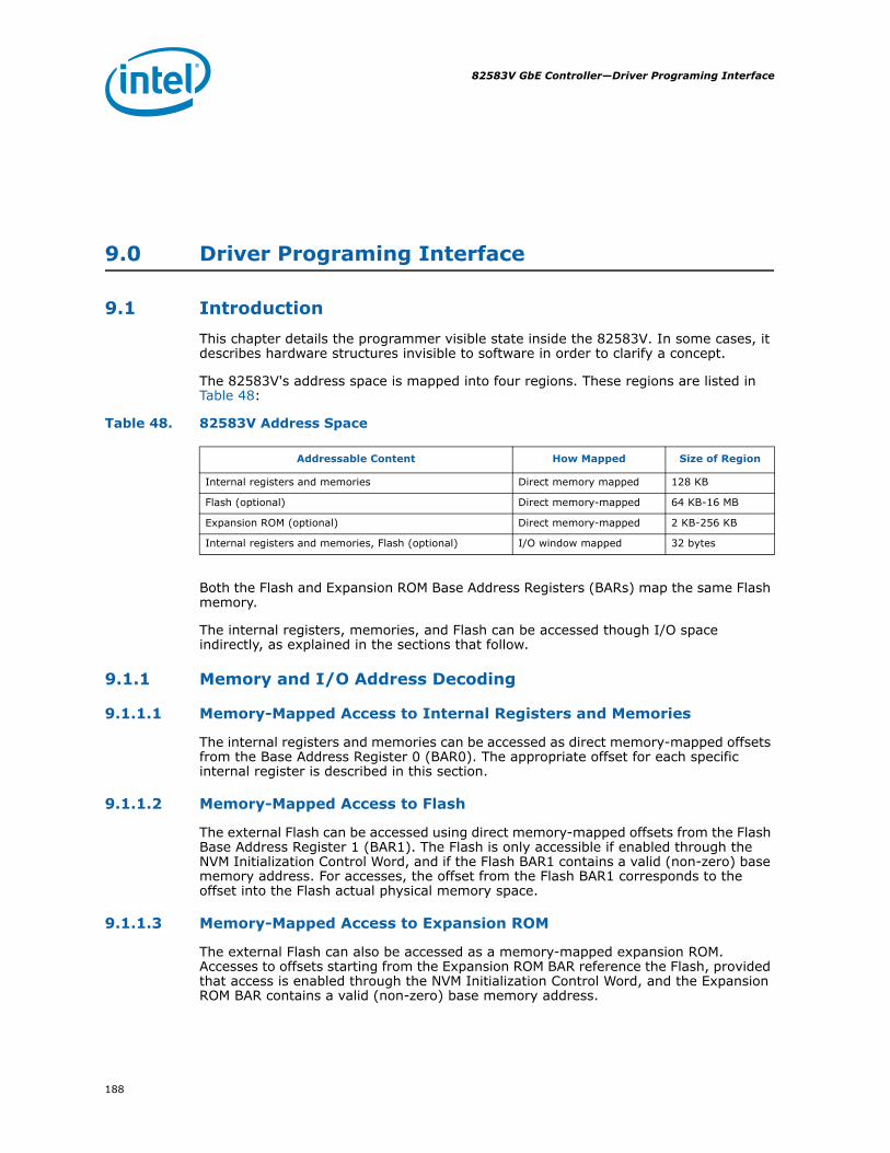
82583V GbE Controller—Driver Programing Interface
188
9.0 Driver Programing Interface
9.1 IntroductionThis chapter details the programmer visible state inside the 82583V. In some cases, it describes hardware structures invisible to software in order to clarify a concept.
The 82583V's address space is mapped into four regions. These regions are listed in Table 48:
Table 48. 82583V Address Space
Both the Flash and Expansion ROM Base Address Registers (BARs) map the same Flash memory.
The internal registers, memories, and Flash can be accessed though I/O space indirectly, as explained in the sections that follow.
9.1.1 Memory and I/O Address Decoding
9.1.1.1 Memory-Mapped Access to Internal Registers and Memories
The internal registers and memories can be accessed as direct memory-mapped offsets from the Base Address Register 0 (BAR0). The appropriate offset for each specific internal register is described in this section.
9.1.1.2 Memory-Mapped Access to Flash
The external Flash can be accessed using direct memory-mapped offsets from the Flash Base Address Register 1 (BAR1). The Flash is only accessible if enabled through the NVM Initialization Control Word, and if the Flash BAR1 contains a valid (non-zero) base memory address. For accesses, the offset from the Flash BAR1 corresponds to the offset into the Flash actual physical memory space.
9.1.1.3 Memory-Mapped Access to Expansion ROM
The external Flash can also be accessed as a memory-mapped expansion ROM. Accesses to offsets starting from the Expansion ROM BAR reference the Flash, provided that access is enabled through the NVM Initialization Control Word, and the Expansion ROM BAR contains a valid (non-zero) base memory address.
Addressable Content How Mapped Size of Region
Internal registers and memories Direct memory mapped 128 KB
Flash (optional) Direct memory-mapped 64 KB-16 MB
Expansion ROM (optional) Direct memory-mapped 2 KB-256 KB
Internal registers and memories, Flash (optional) I/O window mapped 32 bytes

189
Driver Programing Interface—82583V GbE Controller
9.1.1.4 I/O-Mapped Access to Internal Registers, Memories, and Flash
To support pre-boot operation (prior to the allocation of physical memory base addresses), all internal registers, memories, and Flash can be accessed using I/O operations. I/O accesses are supported only if:
• An I/O Base Address Register (BAR) is allocated and mapped (BAR2)• The BAR contains a valid (non-zero) value• I/O address decoding is enabled in the PCIe configuration
When an I/O BAR is mapped, the I/O address range allocated opens a 32-byte window in the system I/O address map. Within this window, two I/O addressable registers are implemented:
• IOADDR• IODATA
The IOADDR register is used to specify a reference to an internal register, memory, or Flash, and then the IODATA register is used as a window to the register, memory or Flash address specified by IOADDR:
9.1.1.4.1 IOADDR (I/O Offset 0x00)
The IOADDR register must always be written as a Dword access. Writes that are less than 32 bits are ignored. Reads of any size return a Dword of data. However, the chipset or CPU might only return a subset of that Dword.
For software programmers, the IN and OUT instructions must be used to cause I/O cycles to be used on the PCIe bus. Because writes must be to a 32-bit quantity, the source register of the OUT instruction must be EAX (the only 32-bit register supported by the OUT command). For reads, the IN instruction can have any size target register, but it is recommended that the 32-bit EAX register be used.
Because only a particular range is addressable, the upper bits of this register are hard coded to zero. Bits 31 through 20 cannot be written to and always read back as 0b.
At hardware reset (Internal Power On Reset) or PCI Reset, this register value resets to 0x00000000. Once written, the value is retained until the next write or reset.
9.1.1.4.2 IODATA (I/O Offset 0x04)
The IODATA register must always be written as a Dword access when the IOADDR register contains a value for the internal register and memories (such as, 0x00000-0x1FFFC). In this case, writes that are less than 32 bits are ignored.
Offset Abbreviation Name R/W Size
0x00 IOADDR
Internal register, internal memory, or Flash location address. 0x00000-0x1FFFF – Internal registers and memories.0x20000-0x7FFFF – Undefined.0x80000-0xFFFFF – Flash.
R/W 4 bytes
0x04 IODATA
Data field for reads or writes to the Internal Register, Internal Memory, or Flash Location as identified by the current value in IOADDR. All 32 bits of this register are read/write-able.
R/W 4 bytes
0x08 – 0x1F Reserved Reserved RO 4 bytes

82583V GbE Controller—Driver Programing Interface
190
The IODATA register may be written as a byte, word, or Dword access when the IOADDR register contains a value for the Flash (such as, 0x80000-0xFFFFF). In this case, the value in IOADDR must be properly aligned to the data value. The following table lists the supported configurations:
Note: Software might have to implement non-obvious code to access the Flash, a byte, or word at a time. Example code that reads a Flash byte is shown here to illustrate the impact of the previous table:
char *IOADDR;
char *IODATA;
IOADDR = IOBASE + 0;
IODATA = IOBASE + 4;
*(IOADDR) = Flash_Byte_Address;
Read_Data = *(IODATA + (Flash_Byte_Address % 4));
Reads to IODATA of any size return a Dword of data. However, the chipset or CPU might only return a subset of that Dword.
For software programmers, the IN and OUT instructions must be used to cause I/O cycles to be used on the PCIe bus. Where 32-bit quantities are required on writes, the source register of the OUT instruction must be EAX (the only 32-bit register supported by the OUT command).
Writes and reads to IODATA when the IOADDR register value is in an undefined range (0x20000-0x7FFFC) should not be performed. Results cannot be determined.
Note: There are no special software timing requirements on accesses to IOADDR or IODATA. All accesses are immediate except when data is not readily available or acceptable. In this case, the 82583V delays the results through normal bus methods (for example, split transaction or transaction retry).
Note: Because a register/memory/Flash read or write takes two I/O cycles to complete, software must provide a guarantee that the two I/O cycles occur as an atomic operation. Otherwise, results can be non-deterministic from the software viewpoint.
9.1.1.4.3 Undefined I/O Offsets
I/O offsets 0x08 through 0x1F are considered to be reserved offsets with the I/O window. Dword reads from these addresses return 0xFFFF; writes to these addresses are discarded.
Access Type 82583V IOADDR Register Bits [1:0]
Target IODATA Access BE[3:0]# bits in Data Phase
Byte (8 bit) 00b 1110b
01b 1101b
10b 1011b
11b 0111b
Word (16 bit) 00b 1100b
10b 0011b
Dword (32 bit) 00b 0000b

191
Driver Programing Interface—82583V GbE Controller
9.1.2 Registers Byte Ordering
This section defines the structure of registers that contain fields carried over the network. Some examples are L2, L3, L4 fields.
The following example is used to describe byte ordering over the wire (hex notation):
where each byte is sent with the Least Significant Bit (LSB) first. That is, the bit order over the wire for this example is
The general rule for register ordering is to use host ordering. Using the previous example, a 6-byte fields (such as, MAC address) is stored in a CSR in the following manner:
The following exceptions use network ordering. Using the previous example, a 16-bit field (such as, EtherType) is stored in a CSR in the following manner:
The following exception uses network ordering:• All ETherType fields
Note: The normal notation as it appears in text books, etc. is to use network ordering. Example: Suppose a MAC address of 00-A0-C9-00-00-00. The order on the network is 00, then A0, then C9, etc. However, the host ordering presentation is:
9.1.3 Register Conventions
All registers in the 82583V are defined to be 32 bits. They should be accessed as 32-bit double-words. There are some exceptions to this rule:
• Register pairs where two 32-bit registers make up a larger logical size.• Accesses to Flash memory (via expansion ROM space, secondary BAR space, or the
I/O space) can be byte, word or double word accesses.
Last First
..., 06 05 04 03 02 01 00
Last First
.... 0000 0011 0000 0010 0000 0001 0000 0000
Byte 3 Byte 2 Byte 1 Byte 0
DW address (N) 0x03 0x02 0x01 0x00
DW address (N+4) 0x05 0x04
Byte 3 Byte 2 Byte 1 Byte 0
(DW aligned) ... ... 0x01 0x00
or (WORD aligned) 0x00 0x01 ... ...
Byte 3 Byte 2 Byte 1 Byte 0
Dword address (N) 00 C9 A0 00
Dword address (N+4) ... ... 00 00

82583V GbE Controller—Driver Programing Interface
192
Reserved bit positions: Some registers contain certain bits that are marked as reserved.
Reads from registers containing reserved bits might return indeterminate values in the reserved bit-positions unless read values are explicitly stated. When read, these reserved bits should be ignored by software.
Reserved and/or undefined addresses: any register address not explicitly declared in this specification should be considered to be reserved, and should not be written to.
Note: Writing to reserved or undefined register addresses can cause indeterminate behavior.
Reads from reserved or undefined configuration register addresses might return indeterminate values unless read values are explicitly stated for specific addresses.
Initial values: most registers define the initial hardware values prior to being programmed. In some cases, hardware initial values are undefined and are listed as such via the text undefined, unknown, or X. Some of these configuration values should be set via NVM configuration or via software in order to insure proper operation. This need is dependent on the function of the bit. Other registers might cite a hardware default which is overridden by a higher-precedence operation. Operations that might supersede hardware defaults can include:
• A valid NVM load• Completion of a hardware operation (such as hardware auto-negotiation)• Writing of a different register whose value is then reflected in another bit
For registers that should be accessed as 32-bit double words, partial writes (less than a 32-bit double word) does not take effect (such as, the write is ignored). Partial reads return all 32 bits of data regardless of the byte enables.
Note: Partial reads to clear-by-read registers (such as, ICR) can have unexpected results since all 32 bits are actually read regardless of the byte enables. Partial reads should not be done.
Note: All statistics registers are implemented as 32-bit registers. Though some logical statistics registers represent counters in excess of 32-bits in width, registers must be accessed using 32-bit operations (such as, independent access to each 32-bit field).
See special notes for VLAN Filter table and multicast table arrays in their specific register definitions.
9.2 Configuration and Status Registers - CSR Space
9.2.1 Register Summary Table
All registers are listed in Section 49. These registers are ordered by grouping and are not necessarily listed in the order that they appear in the address space.

193
Driver Programing Interface—82583V GbE Controller
Table 49. 82583V Register Summary
Category Offset Alias Offset Abbreviation Name RW Link to
Page
General 0x00000 / 0x00004 N/A CTRL Device Control Register RW page 197
General 0x00008 N/A STATUS Device Status Register R page 200
General 0x00010 N/A EEC EEPROM/FLASH Control Register RW/RO page 201
General 0x00014 N/A EERD EEPROM Read Register RW page 203
General 0x00018 N/A CTRL_EXT Extended Device Control Register RW page 203
General 0x0001C N/A FLA Flash Access Register RW page 205
General 0x00020 N/A MDIC MDI Control Register RW page 206
General 0x00028 N/A FCAL Flow Control Address Low RW page 208
General 0x0002C N/A FCAH Flow Control Address High RW page 208
General 0x00030 N/A FCT Flow Control Type RW page 209
General 0x00038 N/A VET VLAN Ether Type RW page 209
General 0x00170 N/A FCTTV Flow Control Transmit Timer Value RW page 209
General 0x05F40 N/A FCRTV Flow Control Refresh Threshold Value RW page 210
General 0x00E00 N/A LEDCTL LED Control RW page 210
General 0x00F00 N/A EXTCNF_CTRL Extended Configuration Control RW page 212
General 0x00F08 N/A EXTCNF_SIZE Extended Configuration Size RW page 212
General 0x01000 N/A PBA Packet Buffer Allocation RW page 213
General 0x1010 N/A EECTL EEPROM Control Register RO page 214
General 0x1014 N/A EEDATA EEPROM Read/Write Data RO page 203
General 0x1018 N/A FLCTL Flash Control Register RO page 214
General 0x101C N/A FLDATA FLASH Read data RO page 214
General 0x1020 N/A FLCNT FLASH Read Counter RO page 214
General 0x01028 N/A FLASHT FLASH Timer Register RW page 214
General 0x0102C N/A EEWR EEPROM Write Register RW page 215
General 0x1030 N/A FLSWCTL SW FLASH Burst Control Register RW page 215
General 0x1034 N/A FLSWDATA SW FLASH Burst Data Register RW page 216
General 0x1038 N/A FLSWCNT SW FLASH Burst Access Counter RW page 216
General 0x0103C N/A FLOP FLASH Opcode Register RW page 216
General 0x1050 N/A FLOL FLEEP Auto Load RW page 216
PCIe 0x05B00 N/A GCR 3GIO Control Register RW page 216
PCIe 0x05B08 N/A FUNCTAG Function–Tag register RW page 218
PCIe 0x05B10 N/A GSCL_1 3GIO Statistic Control Register #1 RW page 218
PCIe 0x05B14 N/A GSCL_2 3GIO Statistic Control Registers #2 RW page 219
PCIe 0x05B18 N/A GSCL_3 3GIO Statistic Control Register #3 RW page 219
PCIe 0x05B1C N/A GSCL_4 3GIO Statistic Control Register #4 RW page 219
PCIe 0x05B20 N/A GSCN_0 3GIO Statistic Counter Registers #0 RW page 219
PCIe 0x05B24 N/A GSCN_1 3GIO Statistic Counter Registers #1 RW page 219

82583V GbE Controller—Driver Programing Interface
194
PCIe 0x05B28 N/A GSCN_2 3GIO Statistic Counter Registers #2 RW page 219
PCIe 0x05B2C N/A GSCN_3 3GIO Statistic Counter Registers #3 RW page 220
PCIe 0x05B50 N/A SWSM Software Semaphore Register RW page 220
PCIe 0x05B64 N/A GCR2 3GIO Control Register 2 RW page 220
Interrupt 0x000C0 N/A ICR Interrupt Cause Read Register RC/WC page 224
Interrupt 0x000C4 N/A ITR Interrupt Throttling Register R/W page 225
Interrupt 0x000C8 N/A ICS Interrupt Cause Set Register W page 227
Interrupt 0x000D0 N/A IMS Interrupt Mask Set/Read Register RW page 228
Interrupt 0x000D8 N/A IMC Interrupt Mask Clear Register W page 229
Interrupt 0x000DC N/A EIAC Interrupt Auto Clear RW page 230
Interrupt 0x000E0 N/A IAM Interrupt Acknowledge Auto–Mask RW page 230
Receive 0x00100 N/A RCTL Receive Control Register RW page 230
Receive 0x02170 N/A PSRCTL Packet Split Receive Control Register RW page 233
Receive 0x02160 0x00168 FCRTL Flow Control Receive Threshold Low RW page 234
Receive 0x02168 0x00160 FCRTH Flow Control Receive Threshold High RW page 234
Receive 0x02800 0x00110 RDBAL0 Receive Descriptor Base Address Low queue 0 RW page 235
Receive 0x02804 0x00114 RDBAH0 Receive Descriptor Base Address High queue 0 RW page 235
Receive 0x02808 0x00118 RDLEN0 Receive Descriptor Length queue 0 RW page 235
Receive 0x02810 0x00120 RDH0 Receive Descriptor Head queue 0 RW page 236
Receive 0x02818 0x00128 RDT0 Receive Descriptor Tail queue 0 RW page 236
Receive 0x02820 0x00108 RDTR Rx Interrupt Delay Timer [Packet Timer] RW page 236
Receive 0x02828 N/A RXDCTL Receive Descriptor Control RW page 237
Receive 0x0282C N/A RADV Receive Interrupt Absolute Delay Timer RW page 238
Receive 0x02C00 N/A RSRPD Receive Small Packet Detect Interrupt R/W page 239
Receive 0x02C08 N/A RAID Receive ACK Interrupt Delay Register RW page 239
Receive 0x05000 N/A RXCSUM Receive Checksum Control RW page 239
Receive 0x05008 N/A RFCTL Receive Filter Control Register RW page 241
Receive 0x05200-0x053FC MTA[127:0] Multicast Table Array RW page 241
Receive 0x05400 0x00040 RAL(0) Receive Address Low (0) RW page 242
Receive 0x05404 0x00044 RAH(0) Receive Address High (0) RW page 242
Receive 0x05408 0x00048 RAL(1) Receive Address Low (1) RW page 242
Receive 0x0540C 0x0004C RAH(1) Receive Address High (1) RW page 242
Receive 0x05600-0x057FC
0x00600-0x007FC VFTA[127:0] VLAN Filter Table Array RW page 244
Receive 0x05600-0x057FC
0x00600-0x006FC VFTA[127:0] VLAN Filter Table Array (n) RW page 244
Receive 0x05478 0x000B8 RAL(15) Receive Address Low (15) RW page 242
Category Offset Alias Offset Abbreviation Name RW Link to
Page

195
Driver Programing Interface—82583V GbE Controller
Receive 0x0547C x000BC RAH(15) Receive Address High (15) RW page 242
Transmit 0x00400 N/A TCTL Transmit Control Register RW page 245
Transmit 0x00410 N/A TIPG Transmit IPG Register RW page 246
Transmit 0x00458 N/A AIT Adaptive IFS Throttle RW page 247
Transmit 0x03800 0x00420 TDBAL Transmit Descriptor Base Address Low RW page 247
Transmit 0x03804 0x00424 TDBAH Transmit Descriptor Base Address High RW page 248
Transmit 0x03808 0x00428 TDLEN Transmit Descriptor Length RW page 248
Transmit 0x03810 0x00430 TDH Transmit Descriptor Head RW page 248
Transmit 0x03818 0x00438 TDT Transmit Descriptor Tail RW page 249
Transmit 0x03840 N/A TARC Transmit Arbitration Count RW page 249
Transmit 0x03820 0x00440 TIDV Transmit Interrupt Delay Value RW page 249
Transmit 0x03828 N/A TXDCTL Transmit Descriptor Control RW page 250
Transmit 0x0382C N/A TADV Transmit Absolute Interrupt Delay Value RW page 252
Statistic 0x04000 N/A CRCERRS CRC Error Count R page 253
Statistic 0x04004 N/A ALGNERRC Alignment Error Count R page 253
Statistic 0x0400C N/A RXERRC RX Error Count R page 253
Statistic 0x04010 N/A MPC Missed Packets Count R page 253
Statistic 0x04014 N/A SCC Single Collision Count R page 254
Statistic 0x04018 N/A ECOL Excessive Collisions Count R page 254
Statistic 0x0401C N/A MCC Multiple Collision Count R page 254
Statistic 0x04020 N/A LATECOL Late Collisions Count R page 254
Statistic 0x04028 N/A COLC Collision Count R page 255
Statistic 0x04030 N/A DC Defer Count R page 255
Statistic 0x04034 N/A TNCRS Transmit with No CRS R page 255
Statistic 0x0403C N/A CEXTERR Carrier Extension Error Count R page 256
Statistic 0x04040 N/A RLEC Receive Length Error Count R page 256
Statistic 0x04048 N/A XONRXC XON Received Count R page 256
Statistic 0x0404C N/A XONTXC XON Transmitted Count R page 256
Statistic 0x04050 N/A XOFFRXC XOFF Received Count R page 257
Statistic 0x04054 N/A XOFFTXC XOFF Transmitted Count R page 257
Statistic 0x04058 N/A FCRUC FC Received Unsupported Count RW page 257
Statistic 0x0405C N/A PRC64 Packets Received [64 Bytes] Count RW page 257
Statistic 0x04060 N/A PRC127 Packets Received [65–127 Bytes] Count RW page 258
Statistic 0x04064 N/A PRC255 Packets Received [128–255 Bytes] Count RW page 258
Statistic 0x04068 N/A PRC511 Packets Received [256–511 Bytes] Count RW page 258
Statistic 0x0406C N/A PRC1023 Packets Received [512–1023 Bytes] Count RW page 258
Category Offset Alias Offset Abbreviation Name RW Link to
Page

82583V GbE Controller—Driver Programing Interface
196
Statistic 0x04070 N/A PRC1522 Packets Received [1024 to Max Bytes] Count RW page 259
Statistic 0x04074 N/A GPRC Good Packets Received Count R page 259
Statistic 0x04078 N/A BPRC Broadcast Packets Received Count R page 259
Statistic 0x0407C N/A MPRC Multicast Packets Received Count R page 260
Statistic 0x04080 N/A GPTC Good Packets Transmitted Count R page 260
Statistic 0x04088 N/A GORCL Good Octets Received Count Low R page 260
Statistic 0x0408C N/A GORCH Good Octets Received Count High R page 260
Statistic 0x04090 N/A GOTCL Good Octets Transmitted Count Low R page 261
Statistic 0x04094 N/A GOTCH Good Octets Transmitted Count High R page 261
Statistic 0x040A0 N/A RNBC Receive No Buffers Count R page 261
Statistic 0x040A4 N/A RUC Receive Undersize Count R page 261
Statistic 0x040A8 N/A RFC Receive Fragment Count R page 262
Statistic 0x040AC N/A ROC Receive Oversize Count R page 262
Statistic 0x040B0 N/A RJC Receive Jabber Count R page 262
Statistic 0x040C0 N/A TORL Total Octets Received R page 263
Statistic 0x040C4 N/A TORH Total Octets Received R page 263
Statistic 0x040C8 N/A TOT Total Octets Transmitted RW page 263
Statistic 0x040D0 N/A TPR Total Packets Received RW page 264
Statistic 0x040D4 N/A TPT Total Packets Transmitted RW page 264
Statistic 0x040D8 N/A PTC64 Packets Transmitted [64 Bytes] Count RW page 264
Statistic 0x040DC N/A PTC127 Packets Transmitted [65–127 Bytes] Count RW page 264
Statistic 0x040E0 N/A PTC255 Packets Transmitted [128–255 Bytes] Count RW page 265
Statistic 0x040E4 N/A PTC511 Packets Transmitted [256–511 Bytes] Count RW page 265
Statistic 0x040E8 N/A PTC1023 Packets Transmitted [512–1023 Bytes] Count RW page 265
Statistic 0x040EC N/A PTC1522 Packets Transmitted [Greater than 1024 Bytes] Count RW page 265
Statistic 0x040F0 N/A MPTC Multicast Packets Transmitted Count RW page 266
Statistic 0x040F4 N/A BPTC Broadcast Packets Transmitted Count RW page 266
Statistic 0x040F8 N/A TSCTC TCP Segmentation Context Transmitted Count RW page 266
Statistic 0x040FC N/A TSCTFC TCP Segmentation Context Transmit Fail Count RW page 266
Statistic 0x04100 N/A IAC Interrupt Assertion Count R page 267
Diagnostic 0x00F10 N/A POEMB PHY OEM Bits Register RW page 296
Diagnostic 0x02410 0x08000 RDFH Receive Data FIFO Head Register RW page 296
Diagnostic 0x02418 0x08008 RDFT Receive Data FIFO Tail Register RW page 297
Diagnostic 0x02420 N/A RDFHS Receive Data FIFO Head Saved Register RW page 297
Diagnostic 0x02428 N/A RDFTS Receive Data FIFO Tail Saved Register RW page 297
Category Offset Alias Offset Abbreviation Name RW Link to
Page

197
Driver Programing Interface—82583V GbE Controller
Note: Certain registers maintain an alias address designed for backward compatibility with software written for previous devices. For these registers, the alias address is shown in Table 49. Those registers can be accessed by software at either the new offset or the alias offset. It is recommended that software written solely for the 82583V, use the new address offset.
9.2.2 General Register Descriptions
9.2.2.1 Device Control Register - CTRL (0x00000 / 0x00004; RW)
Diagnostic 0x02430 N/A RDFPC Receive Data FIFO Packet Count RW page 298
Diagnostic 0x03410 0x08010 TDFH Transmit Data FIFO Head Register RW page 298
Diagnostic 0x03418 0x08018 TDFT Transmit Data FIFO Tail Register RW page 298
Diagnostic 0x03420 N/A TDFHS Transmit Data FIFO Head Saved Register RW page 299
Diagnostic 0x03428 N/A TDFTS Transmit Data FIFO Tail Saved Register RW page 299
Diagnostic 0x03430 N/A TDFPC Transmit Data FIFO Packet Count RW page 299
Diagnostic 0x10000 - 0x17FFF N/A PBM Packet Buffer Memory RW page 299
Diagnostic 0x01008 N/A PBS Packet Buffer Size RW page 300
Field Bit(s) Initial Value Description
FD 0 1b1
Full Duplex0b = Half duplex1b = Full duplex. Controls the MAC duplex setting when explicitly set by software.
Reserved 1 0bReservedWrite as 0b for future compatibility.
GIO Master Disable 2 0b
When set, the 82583V blocks new master requests using this function. Once no master requests are pending by this function, the GIO Master Enable Status bit is set.
Reserved 3 1bReservedSet to 1b.
Reserved 4 0bReservedWrite as 0b for future compatibility.
ASDE 5 0b1
Auto-Speed Detection EnableWhen set to 1b, the MAC ignores the speed indicated by the PHY and attempts to automatically detect the resolved speed of the link and configure itself appropriately. This bit must be set to 0b in the 82583V.
SLU 6 0b1
Set Link UpThe Set Link Up bit MUST be set to 1b to permit the MAC to recognize the link signal from the PHY, which indicates the PHY has gotten the link up, and to receive and transmit data.See Section 6.2.3 for more information about auto-negotiation and link configuration in the various modes.Set link up is normally initialized to 0b. However, if the APM Enable bit is set in the NVM then it is initialized to 1b.
Reserved 7 0bReserved. Must be set to 0b.
Category Offset Alias Offset Abbreviation Name RW Link to
Page

82583V GbE Controller—Driver Programing Interface
198
SPEED 9:8 10b
Speed selectionThese bits can determine the speed configuration and are written by software after reading the PHY configuration through the MDIO interface. These signals are ignored when Auto-Speed Detection is enabled. See Section 6.2.1 for details.00b = 10 Mb/s01b = 100 Mb/s10b = 1000 Mb/s11b =not used
Reserved 10 0bReservedWrite as 0b for future compatibility.
FRCSPD 11 0b1
Force SpeedThis bit is set when software wants to manually configure the MAC speed settings according to the Speed bits. When using a PHY device, note that the PHY device must resolve to the same speed configuration, or software must manually set it to the same speed as the MAC. Note that this bit is superseded by the CTRL_EXT.SPD_BYPS bit which has a similar function.
FRCDPLX 12 0b
Force DuplexWhen set to 1b, software might override the duplex indication from the PHY that is indicated in the FDX to the MAC. Otherwise, the duplex setting is sampled from the PHY FDX indication into the MAC on the asserting edge of the PHY LINK signal. When asserted, the CTRL.FD bit sets duplex.
Reserved 19:13 0x0ReservedReads as 0b.
ADVD3WUC 20 1b
D3Cold WakeUp Capability Advertisement EnableWhen set, D3Cold wakeup capability is advertised based on whether the AUX_PWR advertises presence of auxiliary power (yes if AUX_PWR is indicated, no otherwise). When 0b, however, D3Cold wakeup capability is not advertised even if AUX_PWR presence is indicated.Note: This bit must be set to 1b.
Reserved 25:21 0x0 Reserved
RST 26 0b
Device ResetThis bit performs a reset of the MAC function of the device, as described in Section 9.2.2.2. Normally 0b; writing 1b initiates the reset. This bit is self-clearing.
RFCE 27 0b
Receive Flow Control EnableIndicates that the device responds to the reception of flow control packets. Reception of flow control packets requires the correct loading of the FCAL/H and FCT registers. If auto-negotiation is enabled, this bit is set to the negotiated duplex value. See Section 6.2.3 for more information about auto-negotiation.
TFCE 28 0b
Transmit Flow Control EnableIndicates that the device transmits flow control packets (XON and XOFF frames) based on receiver fullness. If auto-negotiation is enabled, this bit is set to the negotiated duplex value. See Section 6.2.3 for more information about auto-negotiation.
Reserved 29 0bReservedReads as 0b.
VME 30 0b
VLAN Mode EnableWhen set to 1b, all packets transmitted from the 82583V that have VLE set is sent with an 802.1Q header added to the packet. The contents of the header come from the transmit descriptor and from the VLAN type register. On receive, VLAN information is stripped from 802.1Q packets. See Section 7.5.1 for more details.
Field Bit(s) Initial Value Description

199
Driver Programing Interface—82583V GbE Controller
This register, as well as the Extended Device Control (CTRL_EXT) register, controls the major operational modes for the device. While a software write to this register to control device settings, several bits (such as FD and Speed) might be overridden depending on other bit settings and the resultant link configuration determined by the PHY's auto-negotiation resolution. See Section 6.2.3 for a detailed explanation on the link configuration process.
Note: In half-duplex mode, the 82583V transmits carrier extended packets and can receive both carrier extended packets and packets transmitted with bursting.
When using an internal PHY, the FD (duplex) and Speed configuration of the device is normally determined from the link configuration process. Software can specifically override/set these MAC settings via these bits in a forced-link scenario; if so, the values used to configure the MAC must be consistent with the PHY settings.
Manual link configuration is controlled through the PHY's MII management interface.
The ADVD3WUC bit (Advertise D3Cold Wakeup Capability Enable control) enables the AUX_PWR pin to determine whether D3Cold support is advertised. If full 1 Gb/s operation in D3 state is desired but the system's power requirements in this mode would exceed the D3Cold Wakeup-Enabled specification limit (375 mA at 3.3 V dc), this bit can be used to prevent the capability from being advertised to the system.
When using the internal PHY, by default the PHY re-negotiates the lowest functional link speed in D3 and D0u states. The PHYREG 25.2 bit enables this capability to be disabled, in case full 1 Gb/s speed is desired in these states.
Note: The 82583V internal PHY automatically detects an unplugged LAN cable and reduce operational power to the minimal amount required to maintain system operation. Controller operations are not affected, except for the inability to transmit/receive due to the lost link.
Device Reset (RST) might be used to globally reset the entire component. This register is provided primarily as a last-ditch software mechanism to recover from an indeterminate or suspected hung hardware state. Most registers (receive, transmit, interrupt, statistics, etc.), and state machines are set to their power-on reset values, approximating the state following a power-on or PCI reset. However, PCIe configuration registers are not reset, thereby leaving the device mapped into system memory space and accessible by a software device driver. One internal configuration register, the Packet Buffer Allocation (PBA) register, also retains its value through a global reset.
Note: To ensure that global device reset has fully completed and that the 82583V responds to subsequent accesses, designers must wait approximately 1 μs after resetting before attempting to check to see if the bit has cleared or attempting to access (read or write) any other device register.
Before issuing this reset, software has to insure that Tx and Rx processes are stopped by following the procedure described in Section 6.1.3.10.
PHY_RST 31 0b
PHY ResetControls a hardware-level reset to the internal PHY. 0b = Normal (operational).1b = Reset to PHY asserted.
1. These bits are read from the NVM.
Field Bit(s) Initial Value Description

82583V GbE Controller—Driver Programing Interface
200
9.2.2.2 Device Status Register - STATUS (0x00008; R)
FD reflects the actual MAC duplex configuration. This normally reflects the duplex setting for the entire link, as it normally reflects the duplex configuration negotiated between the PHY and link partner (copper link) or MAC and link partner (fiber link).
Link up provides a useful indication of whether something is attached to the port. Successful negotiation of features/link parameters results in link activity. The link start-up process (and consequently the duration for this activity after reset) can be several 100's of μs. It reflects whether the PHY's LINK indication is present. Refer to Section 6.2.3 for more details.
TXOFF indicates the state of the transmit function when symmetrical flow control has been enabled and negotiated with the link partner. This bit is set to 1b when transmission is paused due to the reception of an XOFF frame. It is cleared upon expiration of the pause timer or the receipt of an XON frame.
Field Bit(s) Initial Value Description
FD 0 XFull Duplex0b = half duplex1b = Full duplex. Reflects duplex setting of the MAC and/or link.
LU 1 X
Link Up0b = No link established1b = Link established. For this to be valid, the Set Link Up bit of the Device Control (CTRL.SU) register must be set.
Reserved 3:2 00b Reserved
TXOFF 4 XTransmission PausedIndication of pause state of the transmit function when symmetrical flow control is enabled.
Reserved 5 0b Reserved
SPEED 7:6 X
Link speed setting. Reflects speed setting of the MAC and/or link 00b = 10 Mb/s01b = 100 Mb/s10b = 1000 Mb/s11b = 1000 Mb/s
ASDV 9:8 XAuto-Speed Detection ValueSpeed result sensed by the MAC auto-detection function.
PHYRA 10 1b
PHY Reset AssertedThis bit is read/write. Hardware sets this bit following the assertion of PHY reset. The bit is cleared on writing 0b to it. This bit is used by firmware as an indication for required initialization of the PHY.
Reserved 18:11 0x0 Reserved
GIO Master Enable Status 19 1b
Cleared by the 82583V when the GIO Master Disable bit is set and no master requests are pending by this function. Set otherwise. Indicates that no master requests is issued by this function as long as the GIO Master Disable bit is set.
Reserved 30:20 0x0ReservedReads as 0b.
Reserved 31 0b Reserved

201
Driver Programing Interface—82583V GbE Controller
Speed indicates the actual MAC speed configuration. These bits normally reflect the speed of the actual link, negotiated by the PHY and link partner, and reflected internally from the PHY to the MAC (SPD_IND). These bits might represent the speed configuration of the MAC only, if the MAC speed setting has been forced via software (CTRL.SPEED) or MAC auto-speed detection used. Speed indications are mapped as follows:
00b = 10 Mb/s
01b = 100 Mb/s
10b = 1000 Mb/s
11b = 1000 Mb/s
If Auto-Speed Detection is enabled, the device's speed is configured only once after the link signal is asserted by the PHY.
The ASDV bits are provided for diagnostics purposes only. Even if the MAC speed configuration is not set using this function (ASDE=0b), the ASD calculation can be initiated by software writing a logic one to the CTRL_EXT.ASDCHK bit. The resultant speed detection is reflected in these bits.
9.2.2.3 EEPROM/FLASH Control Register - EEC (0x00010; RW/RO)
Field Bit(s) Initial Value Description
EE_SK 0 0b
Clock input to the NVMWhen EE_GNT is 1b, the EE_SK output signal is mapped to this bit and provides the serial clock input to the NVM. Software clocks the NVM via toggling this bit with successive writes.
EE_CS 1 0b
Chip select input to the NVMWhen EE_GNT is 1b, the EE_CS output signal is mapped to the chip select of the NVM device. Software enables the NVM by writing a 1b to this bit.
EE_DI 2 0bData input to the NVMWhen EE_GNT is 1b, the EE_DI output signal is mapped directly to this bit. Software provides data input to the NVM via writes to this bit.
EE_DO 3 X
Data output bit from the NVMThe EE_DO input signal is mapped directly to this bit in the register and contains the NVM data output. This bit is read-only from the software perspective – writes to this bit have no effect.
FWE 5:4 01b
Flash Write Enable ControlThese two bits control whether writes to the Flash are allowed.00b = Enable Flash erase and block erase.01b = Flash writes and Flash erase disabled.10b = Flash writes enabled.11b = Not allowed.This field enables write and erase instructions from software to the Flash via the Flash BAR and the software DMA registers (FLSW).
EE_REQ 6 0b
Request NVM AccessSoftware must write a 1b to this bit to get direct NVM access. It has access when EE_GNT is 1b. When software completes the access it must write a 0b.
EE_GNT 7 0bGrant NVM AccessWhen this bit is set to 1b, software can access the NVM using the SK, CS, DI, and DO bits.

82583V GbE Controller—Driver Programing Interface
202
This register provides software direct access to the NVM. Software can control the NVM by successive writes to this register. Data and address information is clocked into the EEPROM by software toggling the EE_SK bit of this register with EE_CS set to 1. Data
EE_PRES 8 XNVM PresentSetting this bit to 1b indicates that an NVM (either Flash or EEPROM) is present and has the correct signature field. This bit is read only.
Auto_RD 9 0b
NVM Auto Read DoneWhen set to 1b, this bit indicates that the auto read by hardware from the NVM is done. This bit is set also when the NVM is not present or when its signature is not valid.This field is read only.
Reserved 10 0b Reserved
NVSize 14:11 0010b1
NVM SizeThis field defines the size of the NVM:This field defines the size of the NVM in bytes which equal 128 * 2 ** NVSize. This field is loaded from word 0x0F in the NVM.This field is read only.
NVADDS 16:15 00b
NVM Address SizeThis field defines the address size of the NVM:00b = Reserved.01b = EEPROM with 1 address byte.10b = EEPROM with 2 address bytes.11b = Flash with 3 address bytes.This field is set at power up by the NVMT strapping pin. With the EEPROM, the address length is set following a detection of the signature bits in word 0x12. If an EEPROM is attached to the 82583V and a valid signature is not found, software can modify this field enabling parallel access to empty device. In all other cases writes to this field do not affect the device operation
Reserved 17 0b Reserved
Reserved 18 0b Reserved
Reserved 19 0b Reserved
AUPDEN 20 0b
Enable Autonomous Flash Update1b = Enables the 82583V to update the Flash autonomously. The autonomous update is triggered by write cycles and expiration of the FLASHT timer. 0b = Disables the auto-update logic.
Reserved 21 0b Reserved
SEC1VAL 22 0b
Sector 1 ValidIn case EE_PRES is set, a 0b indicates that S0 in the Flash contains valid signatures. 1b indicates that S1 contains valid signatures. In EEPROM setup or if EE_PRES is not set, the SEC1VAL is 0b.
NVMTYPE 23 0b1
This is a read-only field indicating the NVM type:0b = EEPROM.1b = Flash.This bit is loaded from NVM word 0x0F and is informational only (the design uses strapping to determine the actual NVM type).
Reserved 24 0b Reserved
Reserved 25 0b Reserved
Reserved 31:26 0x0ReservedReads as 0b.
1. These bits are read from the NVM.
Field Bit(s) Initial Value Description

203
Driver Programing Interface—82583V GbE Controller
output from the NVM is latched into bit 3 of this register via the internal 62.5 MHz clock and may be accessed by software via reads of this register. See Section 6.3.8 for details.
Note: Attempts to write to the Flash device when writes are disabled (FWE=01) should not be attempted. Behavior after such an operation is undefined, and can result in component and/or system hangs.
9.2.2.4 EEPROM Read Register - EERD (0x00014; RW)
This register is used by software to cause the 82583V to read individual words in the EEPROM. To read a word, software writes the address to the Read Address field and simultaneously writes a 1b to the Start Read field. The 82583V reads the word from the EEPROM and places it in the Read Data field, setting the Read Done field to 1b. Software can poll this register, looking for a 1b in the Read Done field, and then using the value in the Read Data field.
Note: When this register is used to read a word from the EEPROM, that word is not written to any of the 82583V's internal registers even if it is normally a hardware accessed word.
9.2.2.5 Extended Device Control Register - CTRL_EXT (0x00018; RW)
Field Bit(s) Initial Value Description
START 0 0b
Start ReadWriting a 1b to this bit causes the 82583V to read a 16-bit word at the address stored in the ADDR field from the NVM. The result is stored in the DATA field. This bit is self-clearing
DONE 1 1bRead DoneSet to 1b when the word read completes. Set to 0b when the read is in progress. Writes by software are ignored.
ADDR 15:2 0x0Read AddressThis field is written by software along with Start Read to indicate the word address of the word to read.
DATA 31:16 0x0Read DataData returned from the NVM.
Field Bit(s) Initial Value Description
Reserved 11:0 0x0 Reserved.
ASDCHK 12 0b
ASD (Auto Speed Detection) CheckInitiate an ASD sequence to sense the frequency of the RX_CLK signal from the PHY. The results are reflected in STATUS.ASDV. This bit is self-clearing.
EE_RST 13 0b
EEPROM ResetInitiates a reset-like event to the EEPROM function. This causes the EEPROM to be read as if a PCI_RST_N assertion had occurred. Note: All device functions should be disabled prior to setting this bit. This bit is self-clearing.
Reserved 14 0b1 ReservedShould be set to 0b.

82583V GbE Controller—Driver Programing Interface
204
SPD_BYPS 15 0b
Speed Select BypassWhen set to 1b, all speed detection mechanisms are bypassed and the device is immediately set to the speed indicated by CTRL.SPEED. This provides a method for software to have full control of the speed settings of the device as well as when the change takes place by overriding the hardware clock switching circuitry.
Reserved 16 0b1 ReservedShould be set to 0b.
RO_DIS 17 0b
Relaxed Ordering DisableWhen set to 1b, the device does not request any relaxed ordering transactions regardless of the state of bit 4 (Enable Relaxed Ordering) in the PCIe Device Control register. When this bit is cleared and bit 4 of the PCIe Device Control register is set, the device requests relaxed ordering transactions as described in Section 6.1.3.8.2.
Reserved 18 0b Reserved
DMA Dynamic Gating Enable 19 0b1 When set, this bit enables dynamic clock gating of the DMA and MAC
units.
PHY Power Down Enable 20 1b1 When set, this bit enables the PHY to enter a low-power state.
Reserved 21 0b1 Reserved
Tx LS Flow 22 0b1 Should be set for correct TSO functionality. Refer to Section 7.3.
Tx LS 23 0b1 Should be cleared for correct TSO functionality. Refer to Section 7.3.
EIAME 24 0bExtended Interrupt Auto Mask EnableEIAM is used only upon a read of the EICR register.
Reserved 26:25 00b Reserved
IAME 27 0b
When the IAME (interrupt acknowledge auto-mask enable) bit is set, a read or write to the ICR register has the side effect of writing the value in the IAM register to the IMC register. When this bit is 0b, the feature is disabled.
DRV_LOAD 28 0b
Driver LoadedThis bit should be set by the software device driver after it was loaded, Cleared when the software device driver unloads or PCIe soft reset.
INT_TIMERS_CLEAR_ENA 29 0b
When set, this bit enables the clearing of the interrupt timers following an IMS clear. In this state, successive interrupts occur only after the timers expire again. When cleared, successive interrupts following IMS clear might happen immediately.
Reserved 30 0bReservedReads as 0b.
PBA_Supportr 31 0bPBA SupportThe 82583V behaves in a way supporting legacy INT-x interrupts.Should be cleared when working in INT-x or MSI mode.
1. These bits are read from the NVM.
Field Bit(s) Initial Value Description
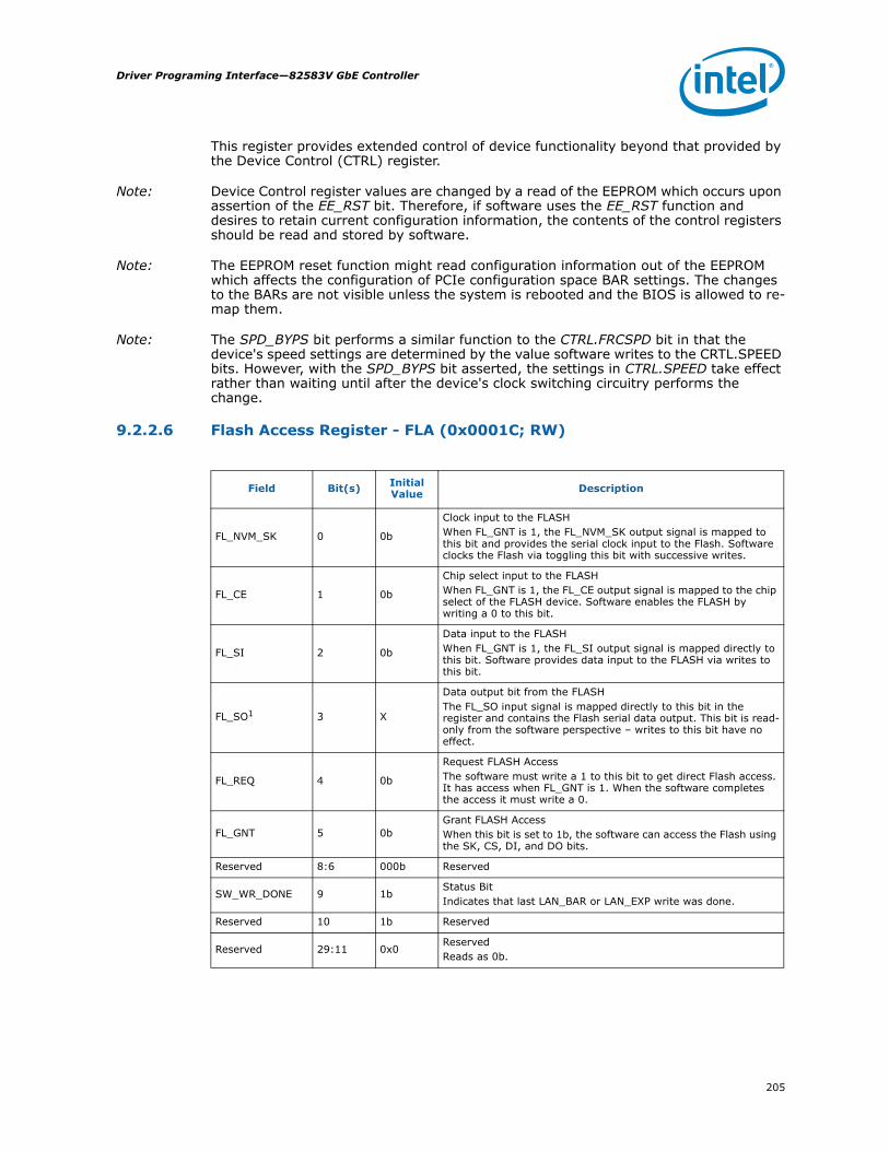
205
Driver Programing Interface—82583V GbE Controller
This register provides extended control of device functionality beyond that provided by the Device Control (CTRL) register.
Note: Device Control register values are changed by a read of the EEPROM which occurs upon assertion of the EE_RST bit. Therefore, if software uses the EE_RST function and desires to retain current configuration information, the contents of the control registers should be read and stored by software.
Note: The EEPROM reset function might read configuration information out of the EEPROM which affects the configuration of PCIe configuration space BAR settings. The changes to the BARs are not visible unless the system is rebooted and the BIOS is allowed to re-map them.
Note: The SPD_BYPS bit performs a similar function to the CTRL.FRCSPD bit in that the device's speed settings are determined by the value software writes to the CRTL.SPEED bits. However, with the SPD_BYPS bit asserted, the settings in CTRL.SPEED take effect rather than waiting until after the device's clock switching circuitry performs the change.
9.2.2.6 Flash Access Register - FLA (0x0001C; RW)
Field Bit(s) Initial Value Description
FL_NVM_SK 0 0b
Clock input to the FLASHWhen FL_GNT is 1, the FL_NVM_SK output signal is mapped to this bit and provides the serial clock input to the Flash. Software clocks the Flash via toggling this bit with successive writes.
FL_CE 1 0b
Chip select input to the FLASHWhen FL_GNT is 1, the FL_CE output signal is mapped to the chip select of the FLASH device. Software enables the FLASH by writing a 0 to this bit.
FL_SI 2 0b
Data input to the FLASHWhen FL_GNT is 1, the FL_SI output signal is mapped directly to this bit. Software provides data input to the FLASH via writes to this bit.
FL_SO1 3 X
Data output bit from the FLASHThe FL_SO input signal is mapped directly to this bit in the register and contains the Flash serial data output. This bit is read-only from the software perspective – writes to this bit have no effect.
FL_REQ 4 0b
Request FLASH AccessThe software must write a 1 to this bit to get direct Flash access. It has access when FL_GNT is 1. When the software completes the access it must write a 0.
FL_GNT 5 0bGrant FLASH AccessWhen this bit is set to 1b, the software can access the Flash using the SK, CS, DI, and DO bits.
Reserved 8:6 000b Reserved
SW_WR_DONE 9 1bStatus BitIndicates that last LAN_BAR or LAN_EXP write was done.
Reserved 10 1b Reserved
Reserved 29:11 0x0ReservedReads as 0b.

82583V GbE Controller—Driver Programing Interface
206
Note: This register provides the software with direct access to the Flash. Software can control the Flash by successive writes to this register. Data and address information is clocked into the Flash by software toggling the FL_NVM_SK bit (0) of this register with FL_CE set to 1. Data output from the Flash is latched into bit 3 of this register via the internal 125 MHz clock and may be accessed by software via reads of this register.
Note: In the 82583V, the FLA register is only reset at Internal Power On Reset and not as legacy devices at a software reset.
9.2.2.7 MDI Control Register - MDIC (0x00020; RW)
This register is used by software to read or write Management Data Interface (MDI) registers in a GMII/MII PHY.
For an MDI read cycle the sequence of events is as follows:1. The CPU performs a PCIe write cycle to the MII register with:
FL_BUSY 30 0b
Flash BusyThis bit is set to 1b while a transaction to the Flash is in progress. While this bit is clear (read as 0b), software can access the Flash.This field is read only.
FL_ER 31 0b
Flash Erase CommandThe command is sent to the Flash only if bits 5:4 in the EEC register are set to 00b. This bit is auto-cleared and read as 0b.Certain Flash vendors do not support this operation.
Field Bit(s) Initial Value Description
DATA 15:0 X
DataIn a Write command, software places the data bits and the MAC shifts them out to the PHY. In a Read command, the MAC reads these bits serially from the PHY and software can read them from this location.
REGADD 20:16 0x0 PHY register address; i.e., Reg 0, 1, 2, … 31.
PHYADD 25:21 0x0PHY Address1 = Gigabit PHY.2 = PCIe PHY.
OP 27:26 0x0
Op-Code01b = MDI write.10b = MDI read. Other values are reserved.
R 28 1b
Ready BitSet to 1b by the 82583V at the end of the MDI transaction (for example, indicates a read or write has been completed). It should be reset to 0b by software at the same time the command is written.
I 29 0bInterrupt EnableWhen set to 1b by software, it causes an Interrupt to be asserted to indicate the end of an MDI cycle.
E 30 0b
ErrorThis bit set is to 1b by hardware when it fails to complete an MDI read. Software should make sure this bit is clear (0b) before making an MDI Read or Write command.
Reserved 31 0b Reserved. Write as 0b for future compatibility.
Field Bit(s) Initial Value Description
207
Driver Programing Interface—82583V GbE Controller
a. Ready = 0b.b. Interrupt Enable bit set to 1b or 0b.c. Op-Code = 10b (read).d. PHYADD = PHY address from the MDI register.e. REGADD = Register address of the specific register to be accessed (0 through
31).2. The MAC applies the following sequence on the MDIO signal to the PHY:
<PREAMBLE><01><10><PHYADD><REGADD><Z> where the Z stands for the MAC tri-stating the MDIO signal.
3. The PHY returns the following sequence on the MDIO signal: <0><DATA><IDLE>.4. The MAC discards the leading bit and places the following 16 data bits in the MII
register.5. The 82583V asserts an interrupt indicating MDI done if the Interrupt Enable bit was
set.6. The 82583V sets the Ready bit in the MII register indicating the read is complete.7. The CPU might read the data from the MII register and issue a new MDI command.
For an MDI write cycle, the sequence of events is as follows:1. The CPU performs a PCIe write cycle to the MII register with:
a. Ready = 0b.b. Interrupt Enable bit set to 1b or 0b.c. Op-Code = 01b (write).d. PHYADD = PHY address from the MDI register.e. REGADD = Register address of the specific register to be accessed (0 through
31).f. Data = Specific data for desired control of the PHY.
2. The MAC applies the following sequence on the MDIO signal to the PHY: <PREAMBLE><01><01><PHYADD><REGADD><10><DATA><IDLE>.
3. The 82583V asserts an interrupt indicating MDI done if the Interrupt Enable bit was set.
4. The 82583V sets the Ready bit in the MII register to indicate step 2 has been completed.
5. The CPU might issue a new MDI command.
Note: An MDI read or write might take as long as 64 μs from the CPU write to the Ready bit assertion.
If an invalid op-code is written by software, the MAC does not execute any accesses to the PHY registers.
If the PHY does not generate a zero as the second bit of the turn-around cycle for reads, the MAC aborts the access, sets the E (error) bit, writes 0xFFFF to the data field to indicate an error condition, and sets the Ready bit.
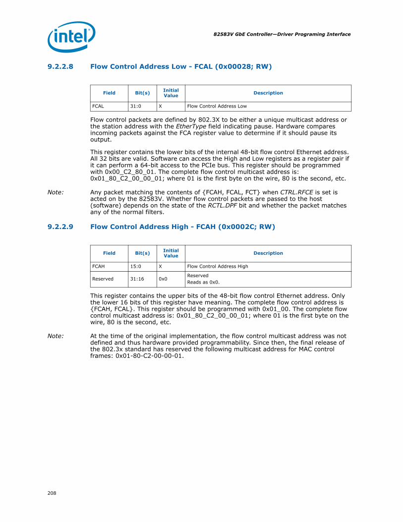
82583V GbE Controller—Driver Programing Interface
208
9.2.2.8 Flow Control Address Low - FCAL (0x00028; RW)
Flow control packets are defined by 802.3X to be either a unique multicast address or the station address with the EtherType field indicating pause. Hardware compares incoming packets against the FCA register value to determine if it should pause its output.
This register contains the lower bits of the internal 48-bit flow control Ethernet address. All 32 bits are valid. Software can access the High and Low registers as a register pair if it can perform a 64-bit access to the PCIe bus. This register should be programmed with 0x00_C2_80_01. The complete flow control multicast address is: 0x01_80_C2_00_00_01; where 01 is the first byte on the wire, 80 is the second, etc.
Note: Any packet matching the contents of {FCAH, FCAL, FCT} when CTRL.RFCE is set is acted on by the 82583V. Whether flow control packets are passed to the host (software) depends on the state of the RCTL.DPF bit and whether the packet matches any of the normal filters.
9.2.2.9 Flow Control Address High - FCAH (0x0002C; RW)
This register contains the upper bits of the 48-bit flow control Ethernet address. Only the lower 16 bits of this register have meaning. The complete flow control address is {FCAH, FCAL}. This register should be programmed with 0x01_00. The complete flow control multicast address is: 0x01_80_C2_00_00_01; where 01 is the first byte on the wire, 80 is the second, etc.
Note: At the time of the original implementation, the flow control multicast address was not defined and thus hardware provided programmability. Since then, the final release of the 802.3x standard has reserved the following multicast address for MAC control frames: 0x01-80-C2-00-00-01.
Field Bit(s) Initial Value Description
FCAL 31:0 X Flow Control Address Low
Field Bit(s) Initial Value Description
FCAH 15:0 X Flow Control Address High
Reserved 31:16 0x0ReservedReads as 0x0.

209
Driver Programing Interface—82583V GbE Controller
9.2.2.10 Flow Control Type - FCT (0x00030; RW)
This register contains the type field hardware uses to recognize a flow control packet. Only the lower 16 bits of this register have meaning. This register should be programmed with 0x88_08. The upper byte is first on the wire FCT[15:8].
Note: At the time of the original implementation, the flow control type field was not defined and thus hardware provided programmability. Since then, the final release of the 802.3x standard has specified the type/length value for MAC control frames as 88-08.
9.2.2.11 VLAN Ether Type - VET (0x00038; RW)
This register contains the type field hardware uses to recognize an 802.1Q (VLAN) Ethernet packet. To be compliant with the 802.3ac standard, this register should be programmed with the value 0x8100. For VLAN transmission the upper byte is first on the wire (VET[15:8]).
9.2.2.12 Flow Control Transmit Timer Value - FCTTV (0x00170; RW)
The 16-bit value in the TTV field is inserted into a transmitted frame (either XOFF frames or any pause frame value in any software transmitted packets). It counts in units of slot time. If software needs to send an XON frame, it must set TTV to 0b prior to initiating the pause frame.
Note: The 82583V uses a fixed slot time value of 64-byte times.
Field Bit(s) Initial Value Description
FCT 15:0 X Flow Control Type
Reserved 31:16 0x0ReservedReads as 0x0
Field Bit(s) Initial Value Description
VET 15:0 0x8100 VLAN Ether Type
Reserved 31:16 0x0ReservedReads as 0x0.
Field Bit(s) Initial Value Description
TTV 15:0 XTransmit Timer ValueIncluded in XOFF frame.
Reserved 31:16 0x0Reads as 0x0.Should be written to 0x0 for future compatibility.

82583V GbE Controller—Driver Programing Interface
210
9.2.2.13 Flow Control Refresh Threshold Value - FCRTV (0x05F40; RW)
9.2.2.14 LED Control - LEDCTL (0x00E00; RW)
Bit Type Reset Description
15:0 RW X
Flow Control Refresh Threshold (FCRT)This value indicates the threshold value of the flow control shadow counter. When the counter reaches this value, and the conditions for a pause state are still valid (buffer fullness above low threshold value), a pause (XOFF) frame is sent to the link partner.The FCRTV timer count interval is the same as other flow control timers and counts at slot times of 64-byte times.If this field contains a zero value, the Flow Control Refresh is disabled.
31:16 RO 0x0ReservedReads as 0x0.Should be written to 0x0 for future compatibility.
Field Bit(s) Initial Value Description
LED0_MODE 3:0 0010b1LED0 (LINK_UP_N) ModeThis field specifies the control source for the LED0 output. An initial value of 0010b selects LINK_UP indication.
Reserved 4 0bReservedRead-only as 0b. Write as 0b for future compatibility.
GLOBAL_BLINK_MODE 5 0b1
Global Blink ModeThis field specifies the blink mode of all LEDs. 0b = Blink at 200 ms on and 200 ms off. 1b = Blink at 83 ms on and 83 ms off.
LED0_IVRT 6 0b1
LED0 (LINK_UP_N) InvertThis field specifies the polarity/ inversion of the LED source prior to output or blink control. 0b = Do not invert LED source.1b = Invert LED source.
LED0_BLINK 7 0b1
LED0 (LINK_UP_N) BlinkThis field specifies whether to apply blink logic to the (inverted) LED control source prior to the LED output. 0b = do not blink asserted LED output.1b = blink asserted LED output.
LED1_MODE 11:8 0011b1LED1 (ACTIVITY_N) ModeThis field specifies the control source for the LED1 output. An initial value of 0011b selects ACTIVITY indication.
Reserved 12 0bReservedRead-only as 0b. Write as 0 for future compatibility.
LED1_BLINK_MODE 13 0b1
LED1 (ACTIVITY_N) Blink ModeThis field needs to be configured with the same value as GLOBAL_BLINK_MODE, it specifies the blink mode of the LED. 0b = Blink at 200 ms on and 200 ms off.1b = Blink at 83 ms on and 83 ms off.
LED1_IVRT 14 0b1 LED1 (ACTIVITY_N) Invert.
LED1_BLINK 15 1b1 LED1 (ACTIVITY_N) Blink

211
Driver Programing Interface—82583V GbE Controller
The following mapping is used to specify the LED control source (MODE) for each LED output:
LED2_MODE 19:16 0110b1LED2 (LINK_100_N) ModeThis field specifies the control source for the LED2 output. An initial value of 0110b selects LINK_100 indication.
Reserved 20 0bReservedRead-only as 0b. Write as 0b for future compatibility.
LED2_BLINK_MODE 21 0b1
LED2 (LINK_100_N) Blink ModeThis field needs to be configured with the same value as GLOBAL_BLINK_MODE, it specifies the blink mode of the LED.0b = Blink at 200 ms on and 200 ms off.1b = Blink at 83 ms on and 83 ms off.
LED2_IVRT 22 0b1 LED2 (LINK_100_N) Invert.
LED2_BLINK 23 0b1 LED2 (LINK_100_N) Blink
Reserved 31:24 0x0 Reserved
1. These bits are read from the NVM.
Field Bit(s) Initial Value Description
MODE Selected Mode Source Indication
0000 LINK_10/1000 Asserted when either 10 or 1000 Mb/s link is established and maintained.
0001 LINK_100/1000 Asserted when either 100 or 1000 Mb/s link is established and maintained.
0010 LINK_UP Asserted when any speed link is established and maintained.
0011 FILTER_ACTIVITY Asserted when link is established and packets are being transmitted or received that passed MAC filtering.
0100 LINK/ACTIVITY Asserted when link is established AND when there is NO transmit or receive activity.
0101 LINK_10 Asserted when a 10 Mb/s link is established and maintained.
0110 LINK_100 Asserted when a 100 Mb/s link is established and maintained.
0111 LINK_1000 Asserted when a 1000 Mb/s link is established and maintained.
1000 Reserved Reserved
1001 FULL_DUPLEX Asserted when the link is configured for full-duplex operation.
1010 COLLISION Asserted when a collision is observed.
1011 ACTIVITY Asserted when link is established and packets are being transmitted or received.
1100 BUS_SIZE Asserted when the device detects a 1-lane PCIe connection.
1101 PAUSED Asserted when the device’s transmitter is flow controlled.
1110 LED_ON Always asserted.
1111 LED_OFF Always de-asserted.

82583V GbE Controller—Driver Programing Interface
212
Notes:1. When LED blink mode is enabled the appropriate LED Invert bit should be set to
zero.2. The dynamic Leds modes (FILTER_ACTIVITY, LINK/ACTIVITY, COLLISION,
ACTIVITY, PAUSED) should be used with LED blink mode enabled.3. When LED blink mode is enabled and CCM PLL is shut, the blinking frequencies are
1/5 of the rates stated in the previous table.
9.2.2.15 Extended Configuration Control - EXTCNF_CTRL (0x00F00; RW)
9.2.2.16 Extended Configuration Size - EXTCNF_SIZE (0x00F08; RW)
Field Bit(s) Initial Value Description
Reserved 31:28 0b Reserved
Reserved 27:16 0x0 Reserved
Reserved 15:8 0x0 Reserved
Reserved 7 0b
MDIO MNG Ownership: Management request for access to MDIO. This is part of the semaphore scheme for MDIO access (Section 4.6.2). This is a RO bit.Note: Use of this register is optional for the 82583V.
Reserved 6 0b
MDIO/NVM HW Ownership: Hardware request fo raccess to MDIO/EEPROM. This is part of the semaphore scheme for MDIO access (Section 4.6.2). This is a RO bit.Note: Use of this register is optional for the 82583V.
Reserved 5 0b
MDIO/NVM SW Ownership: Software request fo raccess to MDIO/EEPROM. This is part of the semaphore scheme for MDIO access (Section 4.6.2). This is a RO bit.Note: Use of this register is optional for the 82583V.
Reserved 4 0b Reserved
Reserved 3 1b Reserved
Reserved 2 0b Reserved
Reserved 1 0b Reserved
Reserved 0 0b Should be set to 0b.
Field Bit(s) Initial Value Description
Reserved 31:8 0x0 Reserved
Reserved 7:0 0x0 Reserved

213
Driver Programing Interface—82583V GbE Controller
9.2.2.17 Packet Buffer Allocation - PBA (0x01000; RW)
This register sets the on-chip receive and transmit storage allocation ratio. The receive allocation value is read/write for the lower 6 bits. The transmit allocation is read only and is calculated based on RXA. The partitioning size is 1 KB.
Note: Programming this register does not automatically re-load or initialize internal packet-buffer RAM pointers. Software must reset both transmit and receive operation (using the global device reset CTRL.RST bit) after changing this register in order for it to take effect. The PBA register itself is not reset by asserting the global reset, but is only reset upon initial hardware power on.
Note: For best performance the transmit buffer allocation should be set to accept two full sized packets.
Note: Transmit packet buffer size should be configured to be more than 4 KB.
Note: The 82583V supports a maximum frame size of 1514 bytes.
9.2.2.18 EEPROM Control Register - EECTL (0x1010; RO)
Note: This register is read/write by firmware and read only by software.
Field Bit(s) Initial Value Description
RXA 15:0 0x0014 Receive packet buffer allocation in KB. Upper 10 bits are read only as 0x0. Default is 20 KB.
TXA 31:16 0x0014 Transmit packet buffer allocation in KB. These bits are read only. Default is 20 KB.
Field Bit(s) Initial Value Description
ADDR 14:0 0x0AddressThis field is written by Start Read or Start write to indicate the EEPROM word address to read or write.
START 15 0bStartWriting a 1b to this bit causes the EEPROM to start the read or write operation according to the write bit.
WRITE 16 0b
WriteThis bit tells the EEPROM if the current operation is read or write.0b = Read.1b = Write.
EEBUSY 17 0bEPROM BusyThis bit indicates that the EEPROM is busy doing an auto read.
Reserved 18 0b Reserved
EE_TRANS_E 19 0bTransactionThis bit indicates that the register is in the middle of a transaction.
Reserved 31:20 0x0 Reserved

82583V GbE Controller—Driver Programing Interface
214
9.2.2.19 EEPROM Read/Write Data - EEDATA (0x1014; RO)
Note: This register is read/write by firmware and read only by software.
9.2.2.20 Flash Control Register - FLCTL (0x1018; RO)
Note: This register is Read-Write by FW and Read-Only by SW.
9.2.2.21 Flash Read Data - FLDATA (0x101C; RO)
Note: This register is Read-Write by FW and Read-Only by SW.
9.2.2.22 Flash Read Counter - FLCNT (0x1020; RO)
Note: This register is Read-Write by FW and Read-Only by SW.
9.2.2.23 Flash Timer Register- FLASHT (0x01028; RW)
Field Bit(s) Initial Value Description
WRDATA 15:0 0x0Write DataData to be written to the EEPROM.
RDDATA 31:16 XRead DataData returned from the EEPROM read.
Field Bit(s) Default Description
FLT 15:0 0x2
Auto Flash Update TimerDefines the idle time from the last write until the 82583V autonomously updates the Flash. The time is measured in FLASHT.FLT x 1024 cycles at 62.5 MHz (or 12.5 MHz when the 125 MHz clock is gated). A value of 0x00 means that the update is not delayed.The update timer is enabled by the Aupden bit in the EEC register.
Reserve 31:16 0x00 Reserved

215
Driver Programing Interface—82583V GbE Controller
9.2.2.24 EEPROM Write Register - EEWR (0x0102C; RW)
Note: EEWR has direct access regardless of a valid signature in the NVM.
9.2.2.25 SW FLASH Burst Control Register - FLSWCTL (0x1030; RW)
Field Bit(s) Default Description
START 0 0b
Start WriteWriting a 1b to this bit causes the 82583V to write a 16-bit word at the address stored in the ADDR field in the external NVM. The data is fetched from the DATA field. This bit is self-clearing.
DONE 1 1bWrite DoneSet to 1b when the write completes. Set to 0b when the write is in progress. Writes by software are ignored.
ADDR 15:2 0x0Write AddressThis field is written by software along with Start Write to indicate the word address of the word to read.
DATA 31:16 0x0Write DataData written to the NVM.
Field Bit(s) Default Description
ADDR 23:0 0x0AddressThis field is written by software along with Start Read or Start write to indicate the Flash address to read or write.
CMD 25:24 00b
CommandIndicates which command should be executed. Valid only when the CMDV bit is set.00b = Reserved.01b = DMA Write command (write up to 256 bytes).10b = Reserved.11b = Reserved.
CMDV 26 0bCommand ValidWhen set, indicates that software issues a new command. Cleared by hardware at the end of the command.
FLBUSY 27 0bFlash BusyThis bit indicates that the Flash is busy processing a Flash transaction and should not be accessed.
Reserved 28 0b Reserved
FLUDONE 29 0bFlash Update DoneThis bit is set by the 82583V when it completes updating the Flash. Software should clear it to zero before it updates the Flash.
DONE 30 1b
Write DoneThis bit clears after CMDV is set by software and is set back again when the Flash write transaction is done.When writing a burst transaction the bit is cleared every time software writes FLSWDATA.
WRDONE 31 1b
Global DoneThis bit clears after the CMDV bit is set by software and is set back again when the all Flash read/write transactions complete. For example, the Flash unit finished to read/write all the requested read/writes.

82583V GbE Controller—Driver Programing Interface
216
9.2.2.26 Software Flash Burst Data Register - FLSWDATA (0x1034; RW)
9.2.2.27 Software Flash Burst Access Counter - FLSWCNT (0x1038; RW)
9.2.2.28 Flash Opcode Register - FLOP (0x0103C; RW)
This register is used by the 82583V to initiate the appropriate instructions to the NVM device.
9.2.2.29 FEEP Auto Load - FLOL (0x01050; RW)
9.2.3 PCIe Register Descriptions
9.2.3.1 3GIO Control Register - GCR (0x05B00; RW)
Field Bit(s) Default Description
NVDATA 31:0 0x0Write NVM DataData written to the NVM.
Field Bit(s) Default Description
Abort 31 0b
AbortWriting a 1b to this bit aborts the current burst operation. It is self-cleared by the Flash interface block when the Abort command has been executed. Abort request is not permitted after writing the last Dword.
Reserved 30:25 0x0 Reserved
NVCNT 24:0 0x0
NVM CounterThis counter holds the size of the Flash burst read or write in Dwords and is also used as the write byte count but in this case it is byte count.
Field Bit(s) Default Description
RAM_PWR_SAVE_EN 0 1b When set to 1b, enables reduced power consumption by clock gating
the 82583V RAMs.
Reserved 7:1 0x0 Auto loaded from NVM 0x11 bits 7:1.
Reserve 31:8 0x0 Reserved
Field Bit(s) Initial Value Description
Disable_timeout_mechanism
31 0b If set, the PCIe time-out mechanism is disabled.
Self_test_result 30 0b If set, a self-test result finished successfully.
Gio_good_l0s 29 0b Force good PCIe L0s training.
Gio_dis_rd_err 28 0b Disable running disparity error of PCIe 108b decoders.

217
Driver Programing Interface—82583V GbE Controller
L1_act_without_L0s_rx
27 0b If set, enables the device to enter ASPM L1 active without any correlation to L0s_rx.
L1_Entry_Latency (LSB)(Read Only)
26:25 11b
Determines the idle time of the PCIe link in L0s state before initiating a transition to L1 state. The initial value is loaded from NVM.00b = 64 μs01b = 256 μs10b = 1 ms11b = 4 ms
L0S_ENTRY_LAT 24 0b
L0s Entry LatencySet to 0b to indicate L0s entry latency is the same as L0s exit latency. Set to 1b to indicate L0s entry latency is (L0s exit latency/4).
L1_Entry_Latency (MSB)(Read Only)
23 1b
Latency000b = 2 μs.001b = 8 μs.010b = 1 6μs.011b = 32 μs.100b = 64 μs.101b = 25 6μs.110b = 1 ms.111b = 4 ms (default).
Reserved 22 0bReservedFor proper operation, must be set to 1b by software during initialization.
Header_log_order 21 0b When set, indicates a need to change the order of the header log in
the error reporting registers.
Reserved 20 0b Reserved
Reserved 19:10 0x0 Reserved
Rx_L0s_Adjustment 9 1b
When set to 1b the reply-timer always adds the required L0s adjustment. When cleared to 0b the adjustment is added only when Tx L0s is active.
Reserved 8:6 0b Reserved
TXDSCR_NOSNOOP 5 0b
Transmit Descriptor Read – No Snoop Indication.Read directly by transaction layer.
TXDSCW_NOSNOOP 4 0b
Transmit Descriptor Write – No Snoop Indication.Read directly by transaction layer.
TXD_NOSNOOP 3 0b
Transmit Data Read – No Snoop Indication.Read directly by transaction layer.
RXDSCR_NOSNOOP 2 0
Receive Descriptor Read – No snoop indication.Read directly by transaction layer.
RXDSCW_NOSNOOP 1 0b
Receive Descriptor Write – No Snoop IndicationRead directly by transaction layer.
RXD_NOSNOOP 0 0b
Receive Data Write – No Snoop IndicationRead directly by transaction layer.
Field Bit(s) Initial Value Description
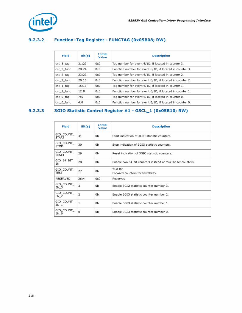
82583V GbE Controller—Driver Programing Interface
218
9.2.3.2 Function–Tag Register - FUNCTAG (0x05B08; RW)
9.2.3.3 3GIO Statistic Control Register #1 - GSCL_1 (0x05B10; RW)
Field Bit(s) Initial Value Description
cnt_3_tag 31:29 0x0 Tag number for event 6/1D, if located in counter 3.
cnt_3_func 28:24 0x0 Function number for event 6/1D, if located in counter 3.
cnt_2_tag 23:29 0x0 Tag number for event 6/1D, if located in counter 2.
cnt_2_func 20:16 0x0 Function number for event 6/1D, if located in counter 2.
cnt_1_tag 15:13 0x0 Tag number for event 6/1D, if located in counter 1.
cnt_1_func 12:8 0x0 Function number for event 6/1D, if located in counter 1.
cnt_0_tag 7:5 0x0 Tag number for event 6/1D, if located in counter 0.
cnt_0_func 4:0 0x0 Function number for event 6/1D, if located in counter 0.
Field Bit(s) Initial Value Description
GIO_COUNT_START 31 0b Start indication of 3GIO statistic counters.
GIO_COUNT_STOP 30 0b Stop indication of 3GIO statistic counters.
GIO_COUNT_RESET 29 0b Reset indication of 3GIO statistic counters.
GIO_64_BIT_EN 28 0b Enable two 64-bit counters instead of four 32-bit counters.
GIO_COUNT_TEST 27 0b
Test BitForward counters for testability.
RESERVED 26:4 0x0 Reserved
GIO_COUNT_EN_3 3 0b Enable 3GIO statistic counter number 3.
GIO_COUNT_EN_2 2 0b Enable 3GIO statistic counter number 2.
GIO_COUNT_EN_1 1 0b Enable 3GIO statistic counter number 1.
GIO_COUNT_EN_0 0 0b Enable 3GIO statistic counter number 0.

219
Driver Programing Interface—82583V GbE Controller
9.2.3.4 3GIO Statistic Control Registers #2- GSCL_2 (0x05B14; RW)
This counter contains the mapping of the event (which counter counts what event).
9.2.3.5 3GIO Statistic Control Register #3 - GSCL_3 (0x05B18; RW)
This counter holds the threshold values needed for some of the event counting. Note that the event increases only after the value passes the threshold boundary.
9.2.3.6 3GIO Statistic Control Register #4 - GSCL_4 (0x05B1C; RW)
This counter holds the threshold values needed for some of the event counting. Note that the event increases only after the value passes the threshold boundary.
9.2.3.7 3GIO Statistic Counter Registers #0 - GSCN_0 (0x05B20; RW)
9.2.3.8 3GIO Statistic Counter Registers #1- GSCN_1 (0x05B24; RW)
9.2.3.9 3GIO Statistic Counter Registers #2- GSCN_2 (0x05B28; RW)
Field Bit(s) Initial Value Description
GIO_EVENT_NUM_3 31:24 0x0 The event number that counter 3 counts
GIO_EVENT_NUM_2 23:16 0x0 The event number that counter counts
GIO_EVENT_NUM_1 15:8 0x0 The event number that counter counts
GIO_EVENT_NUM_0 7:0 0x0 The event number that counter counts
Field Bit(s) Initial Value Description
GIO_FC_TH_0 11:0 0x0Threshold of flow control credits.Optional values: 0 = (256-1).
RESERVED 15:12 0x0 Reserved
GIO_FC_TH_1 27:16 0x0Threshold of flow control credits.Optional values: 0 = (256-1).
RESERVED 31:28 0x0 Reserved
Field Bit(s) Initial Value Description
RESERVED 31:16 0x0 Reserved
GIO_RB_TH 15:10 0x0 Retry buffer threshold.
HOST_COML_TH 9:0 0x0 Completions latency threshold.

82583V GbE Controller—Driver Programing Interface
220
9.2.3.10 3GIO Statistic Counter Registers #3- GSCN_3 (0x05B2C; RW)
9.2.3.11 Software Semaphore Register - SWSM (0x05B50; RW)
9.2.3.12 3GPIO Control Register 2 - GCR2 (0x05B64; RW)
Field Bit(s) Initial Value Description
SMBI 0 1b
This bit is set by hardware when this register is read by the software device driver and cleared when the host driver writes 0b to it.The first time this register is read, the value is 0b. In the next read, the value is 1b (hardware mechanism). The value remains 1b until the software device driver clears it.Note: This bit is typically used by multiple software threads when a device has multiple LAN functions. Since the 82583V is a single port device it is typically not needed. However, if there are multiple software threads of execution accessing the 82583V it could be used as part of a software thread semaphore mechanism.
SWESMBI 1 0b
Software EEPROM Semaphore BitThis bit should be set only by the software device driver (read only to firmware).Note: This bit should not be used in the 82583V. Instead, the EXTCNF_CTRL.MDIO/NVW SW Ownership bit should be used when the software device driver needs to access the PHY or NVM (see Section 4.6.2).Hardware clears this bit on GIO soft reset.
Reserved 2 0b Reserved
Reserved 3 0b Reserved
Reserved 31:4 0x0 Reserved
Field Bit(s) Initial Value Description
Reserved 31:1 0x0 Reserved
Reserved 0 0b Reserved. Must be set to 1b by software during initialization.

221
Driver Programing Interface—82583V GbE Controller
9.2.3.13 Statistic Event Mapping
Transaction layer EventsEvent
Mapping (Hex)
Description
Dwords of Transaction Layer Packet (TLP) transmitted (transferred to the physical layer), include payload and header.
0
Each 125 MHz cycle the counter increases by 1 (1 Dword) or 2 (2 Dwords).Counted: completion, memory, message (not replied).
All types of transmitted packets. 1
Only TLP packets. Each cycle, the counter increase by 1 if TLP packet was transmitted to the link.Counted: completion, memory, message (not replied).
Transmit TLP packets of function #0 2
Each cycle, the counter increases by 1, if the packet was transmitted.Counted: memory, message of function 0 (not replied).
Transmit TLP packets of function #1 3
Each cycle, the counter increases by 1, if the packet was transmitted.Counted: memory, message of function 1 (not replied).
Non posted transmit TLP packets of function #0 4
Each cycle, the counter increases by 1, if the packet was transmitted.Counted: memory (np) of function 0 (not replied).
Non posted transmit TLP packets of function #1 5
Each cycle, the counter increases by 1, if the packet was transmitted.Counted: memory (np) of function 1 (not replied).
Transmit TLP packets of function X and tag Y, according to FUNC_TAG register 6
Each cycle, the counter increases by 1, if the packet was transmitted.Counted: memory, message for a given func# and tag# (not replied).
All types of received packets (TLP only) 1A
Each cycle, the counter increases by 1, if the packet was received.Counted: completion (only good), memory, I/O, config.
Receive TLP packets of function #0 1BEach cycle, the counter increases by 1, if the packet was received.Counted: good completions of func#0.
Reserved 1C Reserved
Receive completion packets 1D
Each cycle, the counter increases by 1, if the packet was received.Counted: good completions for a given func# and tag#.
Clock counter 20 Counts gio cycles.
Bad TLP from LL 21Each cycle, the counter increases by 1, if a bad TLP is received (bad CRC, error reported by AL, misplaced special char, reset in thI of received TLP).
Header Dwords of transaction layer packet transmitted. 25
Only TLP, each 125 MHz cycle the counter increases by 1 (1 Dword of header) or 2 (2 Dwords of the header).Counted: completion, memory, message (not replied).
Header Dwords of Transaction layer packet received. 26
Only TLP, each 125 MHz cycle the counter increases by 1 (1 Dword of header) or 2 (2 Dwords of the header).Counted: completion, memory, message.

82583V GbE Controller—Driver Programing Interface
222
Transaction layer EventsEvent
Mapping (Hex)
Description
Transaction layer stalls transmitting due to lack of flow control credits of the next part.
27
The counter counts the number of times the transaction layer stops transmitting because of this (per packet).Counted: completion, memory, message.
Retransmitted packets. 28The counter increases for each re-transmitted packet.Counted: completion, memory, message.
Stall due to retry buffer full 29
The counter counts the number of times transaction layer stops transmitting because the retry buffer is full (per packet).Counted: completion, memory, message.
Retry buffer is under threshold 2AThreshold specified by software, Retry buffer is under threshold per packet.Counted: completion, memory, message.
Posted Request Header (PRH) flow control credits (of the next part) below threshold
2B
Threshold specified by software.The counter increases each time the number of the specific flow control credits is lower than the threshold.Counted: According to credit type.
Posted Request Data (PRD) flow control credits (of the next part) below threshold
2C
Non-Posted Request Header (NPRH) flow control credits (of the next part) below threshold
2D
Completion Header (CPLH) flow control credits (of the next part) below threshold
2E
Completion Data (CPLD) flow control credits (of the next part) below threshold
2F
Posted Request Header (PRH) flow control credits (of local part) get to zero.
30
Threshold specified by software.The counter increases each time the number of the specific flow control credits reaches the value of zero. (The period that the credit is zero is not counted).Counted: According to credit type.
Non-Posted Request Header (NPRH) flow control credits (of local part) get to zero.
31
Posted Request Data (PRD) flow control credits (of local part) get to zero. 32
Non-Posted Request Data (NPRD) flow control credits (of local part) get to zero.
33
Dwords of TLP received, include payload and header. 34
Each 125 MHz cycle the counter increases by 1 (1 Dword) or 2 (2 Dwords).Counted: completion, memory, message, I/O, config.
Messages packets received 35Each 125 MHz cycle the counter increases by 1.Counted: messages (only good).
Received packets to func_logic. 36Each 125 MHz cycle the counter increases by 1.Counted: memory, I/O, config (only good).

223
Driver Programing Interface—82583V GbE Controller
Host Arbiter Events Event Mapping Description
Average latency of read request – from initialization until end of completions.Estimated latency is ~5 μs
40 + 41
Software selects the client that needs to be tested.The statistic counter counts the number of read requests of the required client.In addition, the accumulated time of all requests are saved in a time accumulator. The average time for read request is:[Accumulated time/number of read requests].(Event 41 is for the counter).
Average latency of read request RTT– from initialization until the first completion is arrived (round trip time). Estimated latency is 1 μs
42 + 43
Software selects the client that needs to be tested.The statistic counter counts the number of read requests of the required client.In addition, the accumulated time of all RTT are saved in a time accumulator. The average time for read request is:[Accumulated time/number of read requests].(Event 43 is for the counter).
Requests that reached time out. 44 Number of requests that reached time out.
Completion latency above threshold 45 + 46
Software selects the client that needs to be tested.Software programs the required threshold (in GSCL_4 – units of 96 ns).One statistic counter counts the time from the beginning of the request until end of completions.The other counter counts the number of events.If the time is above threshold – add 1 to the event counter. (Event 46 is for the counter).
Completion Latency above Threshold – for RTT 47 + 48
Software selects the client that needs to be tested.Software programs the required threshold (in GSCL_4 – units of 96 ns).One statistic counter counts the time from the beginning of the request until first completion arrival.The other counter counts the number of events.If the time is above threshold – add 1 to the event counter.(Event 48 is for the counter).
Link Layer Events Event Mapping Description
Dwords of the packet transmitted (transferred to the physical layer), include payload and header.
50
Include DLLP (Link layer packets) and TLP (transaction layer packets transmitted.Each 125 MHz cycle the counter increases by 1 (1 Dword) or 2 (2 Dwords).
Dwords of packet received (transferred to the physical layer), include payload and header.
51
Include DLLP (Link layer packets) and TLP (transaction layer packets transmitted.Each 125 MHz cycle the counter increases by 1 (1 Dword) or 2 (2 Dwords).
All types of DLLP packets transmitted from link layer. 52 Each cycle, the counter increases by 1, if DLLP packet
was transmitted.
Flow control DLLP transmitted from link layer. 53 Each cycle, the counter increases by 1, if message
was transmitted
Ack DLLP transmitted. 54 Each cycle, the counter increases by 1, if message was transmitted.
All types of DLLP packets received. 55 Each cycle, the counter increases by 1, if DLLP was received.

82583V GbE Controller—Driver Programing Interface
224
9.2.4 Interrupt Register Descriptions
9.2.4.1 Interrupt Cause Read Register - ICR (0x000C0; RC/WC)
Link Layer Events Event Mapping Description
Flow control DLLP received in link layer. 56 Each cycle, the counter increases by 1, if message was received.
Ack DLLP received. 57 Each cycle, the counter increases by 1, if message was received.
Nack DLLP received. 58 Each cycle, the counter increases by 1, if message was transmitted.
Field Bit(s) Initial Value Description
TXDW 0 0b
Transmit Descriptor Written BackSet when hardware processes a descriptor with RS set. If using delayed interrupts (IDE set), the interrupt is delayed until after one of the delayed-timers (TIDV or TADV) expires.
TXQE 1 0bTransmit Queue EmptySet when the last descriptor block for a transmit queue has been used.
LSC 2 0b
Link Status ChangeThis bit is set whenever the link status changes (either from up to down, or from down to up). This bit is affected by the link indication from the PHY.
Reserved 3 0b Reserved
RXDMT0 4 0b
Receive Descriptor Minimum Threshold Hit.This bit indicates that the number of receive descriptors has reached the minimum threshold as set in RCTL.RDMTS. This indicates to the software to load more receive descriptors.
Reserved 5 0b Reserved
RXO 6 0b
Receiver OverrunSet on receive data FIFO overrun. Could be caused either because there are no available buffers or because PCIe receive bandwidth is inadequate.
RXT0 7 0bReceiver Timer InterruptSet when the timer expires.
Reserved 8 0b Reserved
MDAC 9 0bMDIO Access CompleteSet when MDIO access completes. See Section 9.2.7.36 for details.
Reserved 14:10 0x0 Reserved
TXD_LOW 15 0b
Transmit Descriptor Low Threshold HitIndicates that the number of descriptors in the transmit descriptor ring has reached the level specified in the Transmit Descriptor Control register (TXDCTL.LWTHRESH).
SRPD 16 0b
Small Receive Packet DetectedIndicates that a packet of size < RSRPD.SIZE has been detected and transferred to host memory. The interrupt is only asserted if RSRPD.SIZE register has a non-zero value.
ACK 17 0bReceive ACK Frame DetectedIndicates that an ACK frame has been received and the timer in RAID.ACK_DELAY has expired.

225
Driver Programing Interface—82583V GbE Controller
This register contains all interrupt conditions for the 82583V. Whenever an interrupt causing event occurs, the corresponding interrupt bit is set in this register. A PCIe interrupt is generated whenever one of the bits in this register is set, and the corresponding interrupt is enabled via the Interrupt Mask Set/Read register.
Whenever an interrupt causing event occurs, all timers of delayed interrupts are cleared and their cause event is set in the ICR.
Reading from the ICR register has different effects according to the following three cases:
• Case 1 - Interrupt Mask register equals 0x0000 (mask all): ICR content is cleared.• Case 2 - Interrupt was asserted (ICR.INT_ASSERT=1) and auto mask is active: ICR
content is cleared, and the IAM register is written to the IMC register.• Case 3 - Interrupt was not asserted (ICR.INT_ASSERT=0): Read has no side affect.
Writing a 1b to any bit in the register also clears that bit. Writing a 0b to any bit has no effect on that bit.
Note: The INT_ASSERTED bit is a special case. Writing a 1b or 0b to this bit has no affect. It is cleared only when all interrupt sources are cleared.
9.2.4.2 Interrupt Throttling Register - ITR (0x000C4; R/W)
Reserved 19:18 00b Reserved
RxQ0 20 0bReceive Queue 0 InterruptIndicates Receive queue 0 write back or receive queue 0 descriptor minimum threshold hit.
Reserved 21 0b Reserved
TxQ0 22 0bTransmit Queue 0 InterruptIndicates transmit queue 0 write back.
Reserved 23 0b Reserved
Other 24 0b
Other Interrupt. Indicates one of the following interrupts was set:• Link Status Change.• Receiver Overrun.• MDIO Access Complete.• Small Receive Packet Detected.• Receive ACK Frame Detected.
Reserved 30:25 0x0ReservedReads as 0x0.
INT_ASSERTED 31 0b
Interrupt AssertedThis bit is set when the LAN port has a pending interrupt. If the interrupt is enabled in the PCI configuration space, an interrupt is asserted.
Field Bit(s) Initial Value Description
Field Bit(s) Initial Value Description
INTERVAL 15:0 0x0Minimum Inter-Interrupt IntervallThe interval is specified in 256 ns increments. Zero disables interrupt throttling logic.
Reserved 31:16 0x0ReservedShould be written with 0x0 to ensure future compatibility.

82583V GbE Controller—Driver Programing Interface
226
Software can use this register to prevent the condition of repeated, closely spaced, interrupts to the host CPU, asserted by the 82583V, by guaranteeing a minimum delay between successive interrupts.
To independently validate configuration settings, software can use the following algorithm to convert the inter-interrupt interval value to the common interrupts/sec performance metric:
interrupts/sec = (256 x 10-9sec x interval)-1
For example, if the interval is programmed to 500 (decimal), the 82583V guarantees the CPU is not interrupted by it for 128 μs from the last interrupt. The maximum observable interrupt rate from the 82583V should never exceed 7813 interrupts/sec.
Inversely, inter-interrupt interval value can be calculated as:
inter-interrupt interval = (256 x 10-9sec x interrupts/sec) -1
The optimal performance setting for this register is very system and configuration specific. An initial suggested range is 651- 5580 decimal (or 0x28B - 0x15CC).

227
Driver Programing Interface—82583V GbE Controller
9.2.4.3 Interrupt Cause Set Register - ICS (0x000C8; W)
Software uses this register to set an interrupt condition. Any bit written with a 1b sets the corresponding interrupt. This results in the corresponding bit being set in the Interrupt Cause Read register (see Section 9.2.4.1). A PCIe interrupt is also generated if one of the bits in this register is set and the corresponding interrupt is enabled via the Interrupt Mask Set/Read register (see Section 9.2.4.4).
Bits written with 0b are unchanged.
Field Bit(s) Initial Value Description
TXDW 0 X Sets Transmit Descriptor Written Back
TXQE 1 X Sets Transmit Queue Empty
LSC 2 X Sets Link Status Change.
Reserved 3 X Reserved
RXDMT0 4 X Sets Receive Descriptor Minimum Threshold Hit
Reserved 5 X Reserved
RXO 6 XSets Receiver OverrunSet on receive data FIFO overrun.
RXT0 7 X Sets Receiver Timer Interrupt
reserved 8 X Reserved
MDAC 9 X Sets MDIO Access Complete Interrupt
Reserved 10 X Reserved
Reserved 11 X Reserved
Reserved 12 X Reserved
Reserved 14:13 X Reserved
TXD_LOW 15 X Transmit Descriptor Low Threshold Hit
SRPD 16 X Small Receive Packet Detected and Transferred
ACK 17 X Sets Receive ACK Frame Detected
Reserved 19:18 X Reserved
RxQ0 20 0 Sets Receive Queue 0 Interrupt
Reserved 21 0 Reserved
TxQ0 22 0 Sets Transmit Queue 0 Interrupt
Reserved 23 0 Reserved
Other 24 0 Sets Other Interrupt
Reserved 31:25 XReservedShould be written with 0x0 to ensure future compatibility
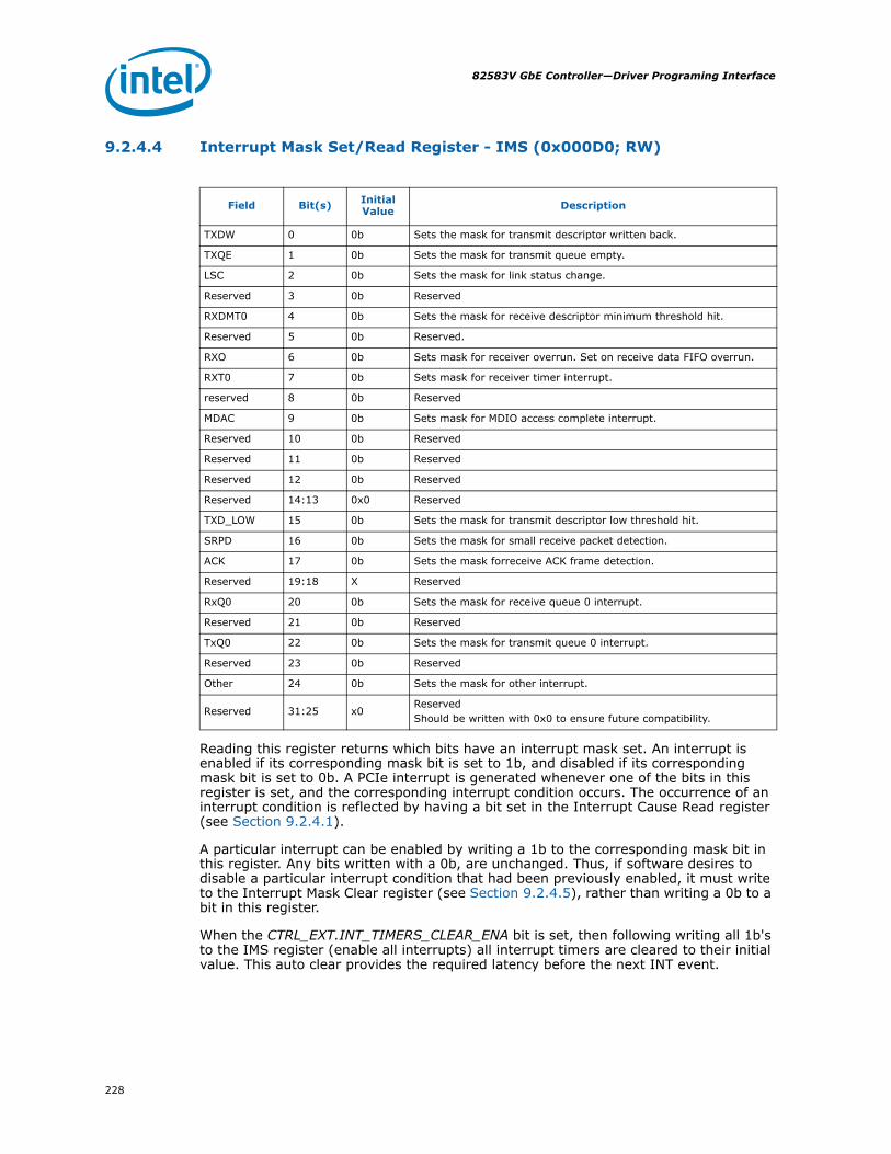
82583V GbE Controller—Driver Programing Interface
228
9.2.4.4 Interrupt Mask Set/Read Register - IMS (0x000D0; RW)
Reading this register returns which bits have an interrupt mask set. An interrupt is enabled if its corresponding mask bit is set to 1b, and disabled if its corresponding mask bit is set to 0b. A PCIe interrupt is generated whenever one of the bits in this register is set, and the corresponding interrupt condition occurs. The occurrence of an interrupt condition is reflected by having a bit set in the Interrupt Cause Read register (see Section 9.2.4.1).
A particular interrupt can be enabled by writing a 1b to the corresponding mask bit in this register. Any bits written with a 0b, are unchanged. Thus, if software desires to disable a particular interrupt condition that had been previously enabled, it must write to the Interrupt Mask Clear register (see Section 9.2.4.5), rather than writing a 0b to a bit in this register.
When the CTRL_EXT.INT_TIMERS_CLEAR_ENA bit is set, then following writing all 1b's to the IMS register (enable all interrupts) all interrupt timers are cleared to their initial value. This auto clear provides the required latency before the next INT event.
Field Bit(s) Initial Value Description
TXDW 0 0b Sets the mask for transmit descriptor written back.
TXQE 1 0b Sets the mask for transmit queue empty.
LSC 2 0b Sets the mask for link status change.
Reserved 3 0b Reserved
RXDMT0 4 0b Sets the mask for receive descriptor minimum threshold hit.
Reserved 5 0b Reserved.
RXO 6 0b Sets mask for receiver overrun. Set on receive data FIFO overrun.
RXT0 7 0b Sets mask for receiver timer interrupt.
reserved 8 0b Reserved
MDAC 9 0b Sets mask for MDIO access complete interrupt.
Reserved 10 0b Reserved
Reserved 11 0b Reserved
Reserved 12 0b Reserved
Reserved 14:13 0x0 Reserved
TXD_LOW 15 0b Sets the mask for transmit descriptor low threshold hit.
SRPD 16 0b Sets the mask for small receive packet detection.
ACK 17 0b Sets the mask forreceive ACK frame detection.
Reserved 19:18 X Reserved
RxQ0 20 0b Sets the mask for receive queue 0 interrupt.
Reserved 21 0b Reserved
TxQ0 22 0b Sets the mask for transmit queue 0 interrupt.
Reserved 23 0b Reserved
Other 24 0b Sets the mask for other interrupt.
Reserved 31:25 x0ReservedShould be written with 0x0 to ensure future compatibility.
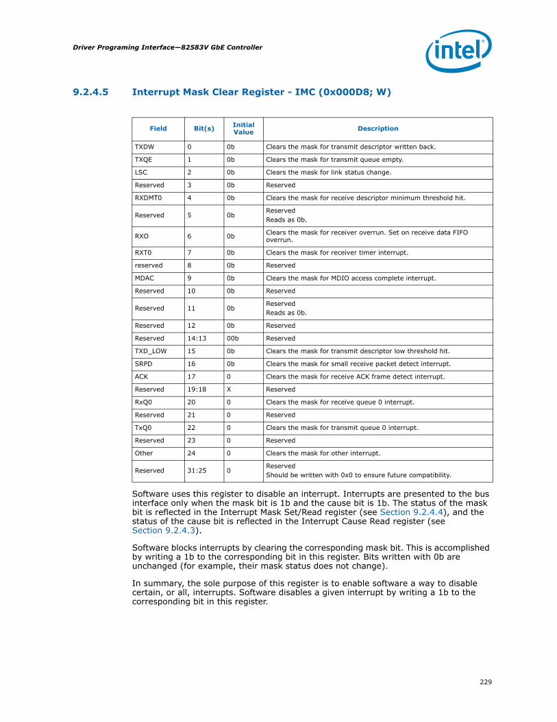
229
Driver Programing Interface—82583V GbE Controller
9.2.4.5 Interrupt Mask Clear Register - IMC (0x000D8; W)
Software uses this register to disable an interrupt. Interrupts are presented to the bus interface only when the mask bit is 1b and the cause bit is 1b. The status of the mask bit is reflected in the Interrupt Mask Set/Read register (see Section 9.2.4.4), and the status of the cause bit is reflected in the Interrupt Cause Read register (see Section 9.2.4.3).
Software blocks interrupts by clearing the corresponding mask bit. This is accomplished by writing a 1b to the corresponding bit in this register. Bits written with 0b are unchanged (for example, their mask status does not change).
In summary, the sole purpose of this register is to enable software a way to disable certain, or all, interrupts. Software disables a given interrupt by writing a 1b to the corresponding bit in this register.
Field Bit(s) Initial Value Description
TXDW 0 0b Clears the mask for transmit descriptor written back.
TXQE 1 0b Clears the mask for transmit queue empty.
LSC 2 0b Clears the mask for link status change.
Reserved 3 0b Reserved
RXDMT0 4 0b Clears the mask for receive descriptor minimum threshold hit.
Reserved 5 0bReservedReads as 0b.
RXO 6 0b Clears the mask for receiver overrun. Set on receive data FIFO overrun.
RXT0 7 0b Clears the mask for receiver timer interrupt.
reserved 8 0b Reserved
MDAC 9 0b Clears the mask for MDIO access complete interrupt.
Reserved 10 0b Reserved
Reserved 11 0bReservedReads as 0b.
Reserved 12 0b Reserved
Reserved 14:13 00b Reserved
TXD_LOW 15 0b Clears the mask for transmit descriptor low threshold hit.
SRPD 16 0b Clears the mask for small receive packet detect interrupt.
ACK 17 0 Clears the mask for receive ACK frame detect interrupt.
Reserved 19:18 X Reserved
RxQ0 20 0 Clears the mask for receive queue 0 interrupt.
Reserved 21 0 Reserved
TxQ0 22 0 Clears the mask for transmit queue 0 interrupt.
Reserved 23 0 Reserved
Other 24 0 Clears the mask for other interrupt.
Reserved 31:25 0ReservedShould be written with 0x0 to ensure future compatibility.

82583V GbE Controller—Driver Programing Interface
230
9.2.4.6 Interrupt Auto Clear- EIAC (0x000DC; RW)
9.2.4.7 Interrupt Acknowledge Auto–Mask - IAM (0x000E0; RW)
9.2.5 Receive Register Descriptions
9.2.5.1 Receive Control Register - RCTL (0x00100; RW)
Field Bit(s) Initial Value Description
Reserved 19:0 0x0 Reserved
Reserved 24:20 0x0 Reserved
Reserved 31:25 0x0 Reserved
Field Bit(s) Initial Value Description
IAM_VALUE 31:0 0x0When the CTRL_EXT.IAME bit is set and the ICR.INT_ASSERT=1b, an ICR read or write has the side effect of writing the contents of this register to the IMC register.
Field Bit(s) Initial Value Description
Reserved 0 0b
ReservedThis bit represented as a hardware reset of the receive-related portion of the device in previous controllers, but is no longer applicable. Only a full device reset CTRL.RST is supported. Write as 0b for future compatibility.
EN 1 0b
EnableThe receiver is enabled when this bit is set to 1b. Writing this bit to 0b, stops reception after receipt of any in progress packet. All subsequent packets are then immediately dropped until this bit is set to 1b.
SBP 2 0b
Store Bad Packets0b = Do not store1b = Store. Note that CRC errors before the SFD are ignored. Any packet must have a valid SFD (RX_DV with no RX_ER in the GMII/MII interface) in order to be recognized by the device (even bad packets)
UPE 3 0bUnicast Promiscuous Enable0b = Disabled.1b = Enabled.
MPE 4 0bMulticast Promiscuous Enable0b = Disabled.1b = Enabled.
LPE 5 0bLong Packet Enable.0b = Disabled (always set to 0b).1b = Enabled (not supported).

231
Driver Programing Interface—82583V GbE Controller
LBM 7:6 00b
Loopback modeShould always be set to 00b.00b = Normal operation (or PHY loopback in GMII/MII mode).01b = MAC Loopback (test mode).10b = Undefined.11b = Undefined.
RDMTS 9:8 00b
Receive Descriptor Minimum Threshold SizeThe corresponding interrupt is set whenever the fractional number of free descriptors becomes equal to RDMTS. Table 50 lists which fractional values correspond to RDMTS values. See Section 9.2.5.7 for details regarding RDLEN.
DTYP 11:10 00b
Descriptor Type00b = Legacy descriptor type.01b = Packet split descriptor type.10b = Reserved.11b = Reserved.
MO 13:12 00b
Multicast OffsetThis determines which bits of the incoming multicast address are used in looking up the bit vector.00b = [47:36].01b = [46:35].10b = [45:34].11b = [43:32].
Reserved 14 0b Reserved
BAM 15 0b
Broadcast Accept Mode0b = Ignore broadcast packets (unless they pass through exact or imperfect filters).1b = Accept broadcast packets.
BSIZE 17:16 0b
Receive Buffer SizeIf RCTL.BSEX = 0b:00b = 2048 bytes.01b = 1024 bytes.10b = 512 bytes.11b = 256 bytes.
If RCTL.BSEX = 1b:00b = reserved; software should not set to this value.01b = 16384 bytes.10b = 8192 bytes.11b = 4096 bytes.BSIZE is only used when DTYP = 00b. When DTYP = 01b, the buffer sizes for the descriptor are controlled by fields in the PSRCTL register.BSIZE is not relevant when FLXBUF is different from 0x0, in that case, FLXBUF determines the buffer size.
VFE 18 0b
VLAN Filter Enable.0b = Disabled (filter table does not decide packet acceptance).1b = Enabled (filter table decides packet acceptance for 802.1Q packets).
CFIEN 19 0b
Canonical Form Indicator Enable0b = Disabled (CFI bit not compared to decide packet acceptance).1b = Enabled (CFI from packet must match next field to accept 802.1Q packets).
CFI 20 0bCanonical Form Indicator Bit ValueIf CFI is set, then 802.1Q packets with CFI equal to this field are accepted; otherwise, the 802.1Q packet is discarded.
Field Bit(s) Initial Value Description

82583V GbE Controller—Driver Programing Interface
232
Hardware discards long packets if LPE is 0b. A long packet is one longer than 1522 bytes. Note that the 82583V does not support setting LPE to 1b.
RDMTS[1,0] determines the threshold value for free receive descriptors according to the following table:
Table 50. RDMTS Values
BSIZE controls the size of the receive buffers and permits software to trade-off descriptor performance versus required storage space. Buffers that are 2048 bytes require only one descriptor per receive packet maximizing descriptor efficiency. Buffers that are 256 bytes maximize memory efficiency at a cost of multiple descriptors for packets longer than 256 bytes.
Three bits control the VLAN filter table. The first determines whether the table participates in the packet acceptance criteria. The next two are used to decide whether the CFI bit found in the 802.1Q packet should be used as part of the acceptance criteria.
Reserved 21 0bReservedShould be written with 0b to ensure future compatibility.
DPF 22 0b
Discard Pause FramesAny valid pause frame is discarded regardless of whether it matches any of the filter registers.0b = Incoming frames subject to filter comparison.1b = Incoming pause frames ignored even if they match filter registers.
PMCF 23 0b
Pass MAC Control Frames0b = Do not (specially) pass MAC control frames.1b = Pass any MAC control frame (type field value of 0x8808) that does not contain the pause opcode of 0x0001.
Reserved 24 0bReservedShould be written with 0b to ensure future compatibility.
BSEX 25 0bBuffer Size ExtensionModifies the buffer size indication (BSIZE). When set to 1b, the original BSIZE values are multiplied by 16.
SECRC 26 0bStrip Ethernet CRC from incoming packet. Do not DMA to host memory.
FLXBUF 30:27 0x0
Determines a flexible buffer size. When this field is 0x0000, the buffer size is determined by BSIZE. If this field is different from 0x0000, the receive buffer size is the number represented in KB. For example, 0x0001 = 1 KB (1024 bytes).
Reserved 31 0bReservedShould be written with 0b to ensure future compatibility.
Field Bit(s) Initial Value Description
RDMTS Free Buffer Threshold
00b 1/2
01b 1/4
10b 1/8
11b Reserved

233
Driver Programing Interface—82583V GbE Controller
DPF controls the DMA function of flow control packets addressed to the station address (RAH/L[0]). If a packet is a valid flow control packet and is addressed to the station address it is not DMA'd to host memory if DPF=1b.
PMCF controls the DMA function of MAC control frames (other than flow control). A MAC control frame in this context must be addressed to either the MAC control frame multicast address or the station address, match the type field and NOT match the pause op-code of 0x0001. If PMCF=1b then frames meeting this criteria are DMA'd to host memory.
The SECRC bit controls whether the hardware strips the Ethernet CRC from the received packet. This stripping occurs prior to any checksum calculations. The stripped CRC is not DMA'd to host memory and is not included in the length reported in the descriptor.
9.2.5.2 Packet Split Receive Control Register - PSRCTL (0x02170; RW)
Note: If software sets a buffer size to zero, all buffers following that one must be set to zero as well. Pointers in the receive descriptors to buffers with a zero size should be set to null pointers.
Field Bit(s) Initial Value Description
BSIZE0 6:0 0x2
Receive Buffer Size for Buffer 0.The value is in 128-byte resolution. Value can be from 128 bytes to 16256 bytes (15.875 KB). Default buffer size is 256 bytes. Software should not program this field to a zero value.
Rsv 7 0bReservedShould be written with 0b to ensure future compatibility.
BSIZE1 13:8 0x4
Receive Buffer Size for Buffer 1.The value is in 1 KB resolution. Value can be from 1 KB to 63 KB. Default buffer size is 4 KB. Software should not program this field to a zero value.
Rsv 15:14 00bReservedShould be written with 00b to ensure future compatibility.
BSIZE2 21:16 0x4
Receive Buffer Size for Buffer 2.The value is in 1 KB resolution. Value can be from 1 KB to 63 KB. Default buffer size is 4 KB. Software can program this field to any value.
Rsv 23:22 00bReservedShould be written with 00b to ensure future compatibility.
BSIZE3 29:24 0x0
Receive Buffer Size for Buffer 3The value is in 1 KB resolution. Value can be from 1 KB to 63 KB. Default buffer size is 0 KB. Software can program this field to any value.
Rsv 31:30 00bReservedShould be written with 0b to ensure future compatibility.
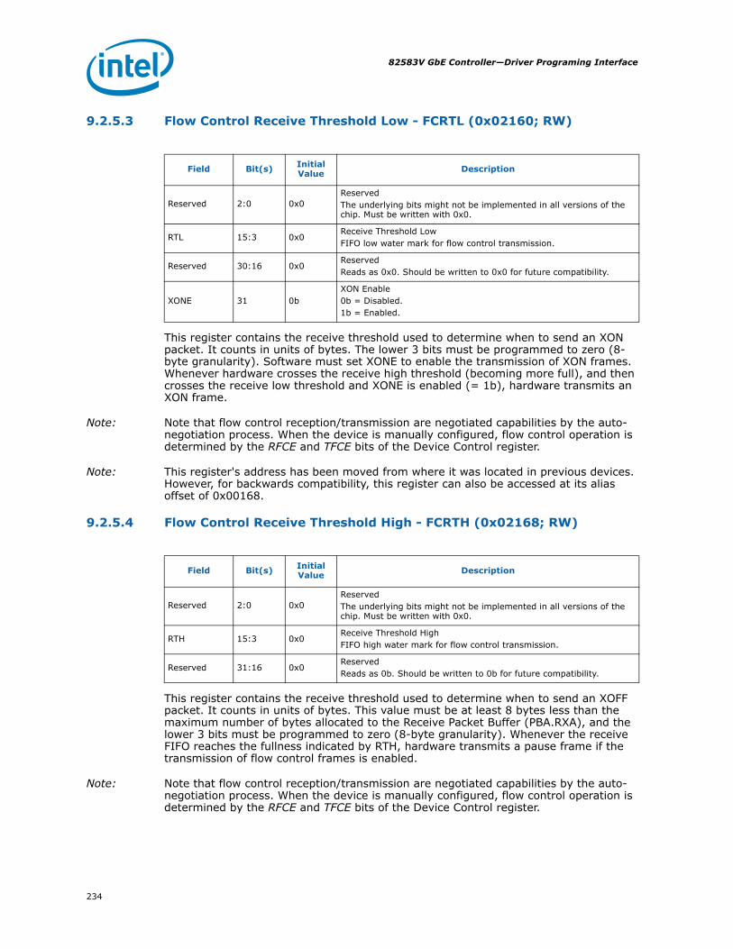
82583V GbE Controller—Driver Programing Interface
234
9.2.5.3 Flow Control Receive Threshold Low - FCRTL (0x02160; RW)
This register contains the receive threshold used to determine when to send an XON packet. It counts in units of bytes. The lower 3 bits must be programmed to zero (8-byte granularity). Software must set XONE to enable the transmission of XON frames. Whenever hardware crosses the receive high threshold (becoming more full), and then crosses the receive low threshold and XONE is enabled (= 1b), hardware transmits an XON frame.
Note: Note that flow control reception/transmission are negotiated capabilities by the auto-negotiation process. When the device is manually configured, flow control operation is determined by the RFCE and TFCE bits of the Device Control register.
Note: This register's address has been moved from where it was located in previous devices. However, for backwards compatibility, this register can also be accessed at its alias offset of 0x00168.
9.2.5.4 Flow Control Receive Threshold High - FCRTH (0x02168; RW)
This register contains the receive threshold used to determine when to send an XOFF packet. It counts in units of bytes. This value must be at least 8 bytes less than the maximum number of bytes allocated to the Receive Packet Buffer (PBA.RXA), and the lower 3 bits must be programmed to zero (8-byte granularity). Whenever the receive FIFO reaches the fullness indicated by RTH, hardware transmits a pause frame if the transmission of flow control frames is enabled.
Note: Note that flow control reception/transmission are negotiated capabilities by the auto-negotiation process. When the device is manually configured, flow control operation is determined by the RFCE and TFCE bits of the Device Control register.
Field Bit(s) Initial Value Description
Reserved 2:0 0x0ReservedThe underlying bits might not be implemented in all versions of the chip. Must be written with 0x0.
RTL 15:3 0x0Receive Threshold LowFIFO low water mark for flow control transmission.
Reserved 30:16 0x0ReservedReads as 0x0. Should be written to 0x0 for future compatibility.
XONE 31 0bXON Enable0b = Disabled.1b = Enabled.
Field Bit(s) Initial Value Description
Reserved 2:0 0x0ReservedThe underlying bits might not be implemented in all versions of the chip. Must be written with 0x0.
RTH 15:3 0x0Receive Threshold HighFIFO high water mark for flow control transmission.
Reserved 31:16 0x0ReservedReads as 0b. Should be written to 0b for future compatibility.

235
Driver Programing Interface—82583V GbE Controller
Note: This register's address has been moved from where it was located in previous devices. However, for backwards compatibility, this register can also be accessed at its alias offset of 0x00160.
9.2.5.5 Receive Descriptor Base Address Low - RDBAL (0x02800; RW)
This register contains the lower bits of the 64-bit descriptor base address. The lower 4 bits are always ignored. The Receive Descriptor Base Address must point to a 16-byte aligned block of data.
Note: This register's address has been moved from where it was located in previous devices. However, for backwards compatibility, this register can also be accessed at its alias offset of 0x00110.
9.2.5.6 Receive Descriptor Base Address High - RDBAH (0x02804; RW)
This register contains the upper 32 bits of the 64-bit descriptor base address.
Note: This register's address has been moved from where it was located in previous devices. However, for backwards compatibility, this register can also be accessed at its alias offset of 0x00114.
9.2.5.7 Receive Descriptor Length - RDLEN (0x02808; RW)
This register sets the number of bytes allocated for descriptors in the circular descriptor buffer. It must be 128-byte aligned.
Note: This register's address has been moved from where it was located in previous devices. However, for backwards compatibility, this register can also be accessed at its alias offset of 0x00118.
Field Bit(s) Initial Value Description
0 3:0 0x0 Ignored on writes. Returns 0b on reads.
RDBAL 31:4 X Receive Descriptor Base Address Low
Field Bit(s) Initial Value Description
RDBAH 31:0 X Receive Descriptor Base Address [63:32]
Field Bit(s) Initial Value Description
0 6:0 0x0 Ignore on write. Reads back as 0x0.
LEN 19:7 0x0 Descriptor Length
Reserved 31:20 0x0 Reads as 0x0. Should be written to 0x0 for future compatibility.
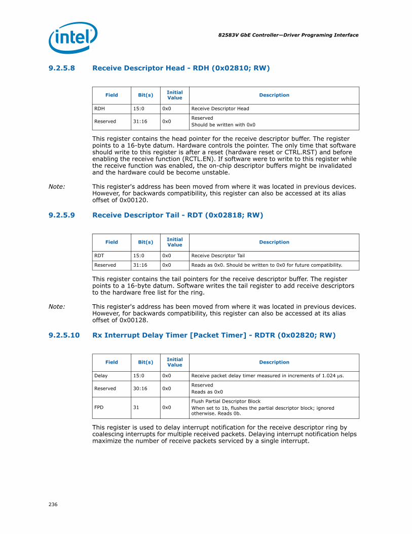
82583V GbE Controller—Driver Programing Interface
236
9.2.5.8 Receive Descriptor Head - RDH (0x02810; RW)
This register contains the head pointer for the receive descriptor buffer. The register points to a 16-byte datum. Hardware controls the pointer. The only time that software should write to this register is after a reset (hardware reset or CTRL.RST) and before enabling the receive function (RCTL.EN). If software were to write to this register while the receive function was enabled, the on-chip descriptor buffers might be invalidated and the hardware could be become unstable.
Note: This register's address has been moved from where it was located in previous devices. However, for backwards compatibility, this register can also be accessed at its alias offset of 0x00120.
9.2.5.9 Receive Descriptor Tail - RDT (0x02818; RW)
This register contains the tail pointers for the receive descriptor buffer. The register points to a 16-byte datum. Software writes the tail register to add receive descriptors to the hardware free list for the ring.
Note: This register's address has been moved from where it was located in previous devices. However, for backwards compatibility, this register can also be accessed at its alias offset of 0x00128.
9.2.5.10 Rx Interrupt Delay Timer [Packet Timer] - RDTR (0x02820; RW)
This register is used to delay interrupt notification for the receive descriptor ring by coalescing interrupts for multiple received packets. Delaying interrupt notification helps maximize the number of receive packets serviced by a single interrupt.
Field Bit(s) Initial Value Description
RDH 15:0 0x0 Receive Descriptor Head
Reserved 31:16 0x0ReservedShould be written with 0x0
Field Bit(s) Initial Value Description
RDT 15:0 0x0 Receive Descriptor Tail
Reserved 31:16 0x0 Reads as 0x0. Should be written to 0x0 for future compatibility.
Field Bit(s) Initial Value Description
Delay 15:0 0x0 Receive packet delay timer measured in increments of 1.024 μs.
Reserved 30:16 0x0ReservedReads as 0x0
FPD 31 0x0Flush Partial Descriptor BlockWhen set to 1b, flushes the partial descriptor block; ignored otherwise. Reads 0b.

237
Driver Programing Interface—82583V GbE Controller
This feature operates by initiating a countdown timer upon successfully receiving each packet to system memory. If a subsequent packet is received before the timer expires, the timer is re-initialized to the programmed value and re-starts its countdown. If the timer expires due to not having received a subsequent packet within the programmed interval, pending receive descriptor write backs are flushed and a receive timer interrupt is generated.
Setting the value to zero represents no delay from a receive packet to the interrupt notification, and results in immediate interrupt notification for each received packet.
Writing this register with FPD set initiates an immediate expiration of the timer, causing a write back of any consumed receive descriptors pending write back, and results in a receive timer interrupt in the ICR.
Receive interrupts due to a Receive Absolute Timer (RADV) expiration cancels a pending RDTR interrupt. The RDTR countdown timer is reloaded but halted, so as to avoid generation of a spurious second interrupt after the RADV has been noted, but can be restarted by a subsequent received packet.
Note: FPD is self clearing.
Note: This register's address has been moved from where it was located in previous devices. However, for backwards compatibility, this register can also be accessed at its alias offset of 0x00108.
9.2.5.11 Receive Descriptor Control - RXDCTL (0x02828; RW)
Note: Any value written to RXDCTL0 is automatically written to RXDCTL1. Writes to RXDCTL1 affects RXDCTL1 only.
This register controls the fetching and write back of receive descriptors. The three threshold values are used to determine when descriptors are read from and written to host memory. The values can be in units of cache lines or descriptors (each descriptor is 16 bytes) based on the GRAN flag. If GRAN=0b (specifications are in cache-line granularity), the thresholds specified (based on the cache line size specified in the PCIe header CLS field) must not represent greater than 31 descriptors.
Field Bit(s) Initial Value Description
PTHRESH 5:0 0x00 Prefetch Threshold
Rsv 7:6 0x00 Reserved
HTHRESH 13:8 0x00 Host Threshold
Reserved 14 0b Reserved
Rsv 15 0b Reserved
WTHRESH 21:16 0x01 Write-Back Threshold
Rsv 23:22 00b Reserved
GRAN 24 0b
GranularityUnits for the thresholds in this register.0b = Cache lines.1b = Descriptors.
Rsv 31:25 0x0 Reserved

82583V GbE Controller—Driver Programing Interface
238
PTHRESH is used to control when a prefetch of descriptors are considered. This threshold refers to the number of valid, unprocessed receive descriptors the chip has in its on-chip buffer. If this number drops below PTHRESH, the algorithm considers pre-fetching descriptors from host memory. This fetch does not happen however, unless there are at least HTHRESH valid descriptors in host memory to fetch.
Note: HTHRESH should be given a non-zero value whenever PTHRESH is used.
WTHRESH controls the write back of processed receive descriptors. This threshold refers to the number of receive descriptors in the on-chip buffer which are ready to be written back to host memory. In the absence of external events (explicit flushes), the write back occurs only after at least WTHRESH descriptors are available for write back.
Note: Possible values:
GRAN = 1b (descriptor granularity):
PTHRESH = 0..47
WTHRESH = 0..63
HTHRESH = 0..63
GRAN = 0 (cacheline granularity):
PTHRESH = 0..3 (for 16 descriptors cacheline - 256 bytes)
WTHRESH = 0..3
HTHRESH = 0..4
Note: For any WTHRESH value other than zero - packet and absolute timers must get a non-zero value for WTHRESH feature to take affect.
Note: Since the default value for write-back threshold is one, the descriptors are normally written back as soon as one cache line is available. WTHRESH must contain a non-zero value to take advantage of the write-back bursting capabilities of the 82583V.
9.2.5.12 Receive Interrupt Absolute Delay Timer- RADV (0x0282C; RW)
If the packet delay timer is used to coalesce receive interrupts, it ensures that when receive traffic abates, an interrupt is generated within a specified interval of no receives. During times when receive traffic is continuous, it might be necessary to ensure that no receive remains unnoticed for too long an interval. This register can be used to ensure that a receive interrupt occurs at some predefined interval after the first packet is received.
When this timer is enabled, a separate absolute count-down timer is initiated upon successfully receiving each packet to system memory. When this absolute timer expires, pending receive descriptor write backs are flushed and a receive timer interrupt is generated.
Field Bit(s) Initial Value Description
Delay 15:0 0x0 Receive absolute delay timer measured in increments of 1.024 μs (0= disabled).
Reserved 31:16 0x0ReservedReads as 0x0.

239
Driver Programing Interface—82583V GbE Controller
Setting this register to 0x0 disables the absolute timer mechanism (the RDTR register should be used with a value of 0x0 to cause immediate interrupts for all receive packets).
Receive interrupts due to a Receive Packet Timer (RDTR) expiration cancels a pending RADV interrupt. If enabled, the RADV count-down timer is reloaded but halted, so as to avoid generation of a serious second interrupt after the RDTR has been noted.
9.2.5.13 Receive Small Packet Detect Interrupt- RSRPD (0x02C00; R/W)
9.2.5.14 Receive ACK Interrupt Delay Register - RAID (0x02C08; RW)
If an immediate (non-scheduled) interrupt is desired for any received ACK frame, the ACK_DELAY should be set to x00.
9.2.5.15 Receive Checksum Control - RXCSUM (0x05000; RW)
The Receive Checksum Control register controls the receive checksum offloading features of the 82583V. The 82583V supports the offloading of three receive checksum calculations: the packet checksum, the IP header checksum, and the TCP/UDP checksum.
Field Bit(s) Initial Value Description
SIZE 11:0 0x0
If the interrupt is enabled any received packet of size <= SIZE asserts an interrupt. SIZE is specified in bytes and includes the headers and the CRC. It does not include the VLAN header in size calculation if it is stripped.
Reserved 31:12 X Reserved.
Field Bit(s) Initial Value Description
RSV 16:31 0x0 Reserved
ACK_DELAY 15:0 0x0
ACK delay timer measured in increments of 1.024 μs. When the receive ACK frame detect interrupt is enabled in the IMS register, ACK packets being received uses a unique delay timer to generate an interrupt. When an ACK is received, an absolute timer loads to the value of ACK_DELAY. The interrupt signal is set only when the timer expires. If another ACK packet is received while the timer is counting down, the timer is not reloaded to ACK_DELAY.
Field Bit(s) Initial Value Description
PCSS 7:0 0x0 Packet Checksum Start
IPOFLD 8 1b IP Checksum Offload Enable
TUOFLD 9 1b TCP/UDP Checksum Offload Enable
Reserved 10 0b Reserved
CRCOFL 11 0b CRC32 Offload Enable
IPPCSE 12 0b IP Payload Checksum Enable
PCSD 13 0b Packet Checksum Disable
Reserved 31:14 0x0 Reserved
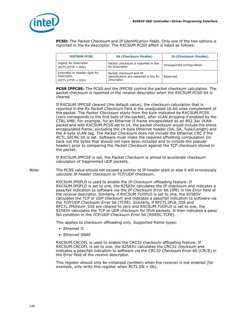
82583V GbE Controller—Driver Programing Interface
240
PCSD: The Packet Checksum and IP Identification fields. Only one of the two options is reported in the Rx descriptor. The RXCSUM.PCSD affect is listed as follows:
PCSS IPPCSE: The PCSS and the IPPCSE control the packet checksum calculation. The packet checksum is reported in the receive descriptor when the RXCSUM.PCSD bit is cleared.
If RXCSUM.IPPCSE cleared (the default value), the checksum calculation that is reported in the Rx Packet Checksum field is the unadjusted 16-bit ones complement of the packet. The Packet Checksum starts from the byte indicated by RXCSUM.PCSS (zero corresponds to the first byte of the packet), after VLAN stripping if enabled by the CTRL.VME. For example, for an Ethernet II frame encapsulated as an 802.3ac VLAN packet and with RXCSUM.PCSS set to 14, the packet checksum would include the entire encapsulated frame, excluding the 14-byte Ethernet header (DA, SA, Type/Length) and the 4-byte VLAN tag. The Packet Checksum does not include the Ethernet CRC if the RCTL.SECRC bit is set. Software must make the required offsetting computation (to back out the bytes that should not have been included and to include the pseudo-header) prior to comparing the Packet Checksum against the TCP checksum stored in the packet.
If RXCSUM.IPPCSE is set, the Packet Checksum is aimed to accelerate checksum calculation of fragmented UDP packets.
Note: The PCSS value should not exceed a pointer to IP header start or else it will erroneously calculate IP header checksum or TCP/UDP checksum.
RXCSUM.IPOFLD is used to enable the IP Checksum offloading feature. If RXCSUM.IPOFLD is set to one, the 82583V calculates the IP checksum and indicates a pass/fail indication to software via the IP Checksum Error bit (IPE) in the Error field of the receive descriptor. Similarly, if RXCSUM.TUOFLD is set to one, the 82583V calculates the TCP or UDP checksum and indicates a pass/fail indication to software via the TCP/UDP Checksum Error bit (TCPE). Similarly, if RFCTL.IPv6_DIS and RFCTL.IP6Xsum_DIS are cleared to zero and RXCSUM.TUOFLD is set to one, the 82583V calculates the TCP or UDP checksum for IPv6 packets. It then indicates a pass/fail condition in the TCP/UDP Checksum Error bit (RDESC.TCPE).
This applies to checksum offloading only. Supported frame types:• Ethernet II• Ethernet SNAP
RXCSUM.CRCOFL is used to enable the CRC32 checksum offloading feature. If RXCSUM.CRCOFL is set to one, the 82583V calculates the CRC32 checksum and indicates a pass/fail indication to software via the CRC32 Checksum Error bit (CRCE) in the Error field of the receive descriptor.
This register should only be initialized (written) when the receiver is not enabled (for example, only write this register when RCTL.EN = 0b).
RXCSUM.PCSD 0b (Checksum Enable) 1b (Checksum Disable)
Legacy Rx Descriptor(RCTL.DTYP = 00b)
Packet checksum is reported in the Rx Descriptor Unsupported configuration.
Extended or Header Split Rx Descriptor(RCTL.DTYP = 01b)
Packet checksum and IP identification are reported in the Rx Descriptor
Reserved.

241
Driver Programing Interface—82583V GbE Controller
9.2.5.16 Receive Filter Control Register - RFCTL (0x05008; RW)
9.2.5.17 Multicast Table Array - MTA[127:0] (0x05200-0x053FC; RW)
Field Bit(s) Initial Value Description
ISCSI_DIS 0 0biSCSI Disable Disable the iSCSI filtering.
ISCSI_DWC 5:1 0x0iSCSI Dword Count This field indicates the Dword count of the iSCSI header, which is used for packet split mechanism.
NFSW_DIS 6 0bNFS Write Disable Disable filtering of NFS write request headers.
NFSR_DIS 7 0bNFS Read Disable Disable filtering of NFS read reply headers.
NFS_VER 9:8 00b
NFS Version00b = NFS version 2.01b = NFS version 3.10b = NFS version 4.11b = Reserved for future use.
IPv6_dis 10 0 bIPv6 Disable.Disable IPv6 packet filtering.
IP6Xsum_dis 11 0bIPv6 Xsum Disable Disable XSUM on IPv6 packets.
ACKDIS 12 0 bACK Accelerate DisableWhen this bit is set, the 82583V does not accelerate interrupt on TCP ACK packets.
ACKD_DIS 13 0b
ACK data Disable1b = The 82583V recognizes ACK packets according to the ACK bit in the TCP header + No –CP data 0b = The 82583V recognizes ACK packets according to the ACK bit only.This bit is relevant only if the ACKDIS bit is not set.
IPFRSP_DIS 14 0bIP Fragment Split DisableWhen this bit is set, the header of IP fragmented packets are not set.
EXSTEN 15 0b
Extended status EnableWhen the EXSTEN bit is set or when the packet split receive descriptor is used, the 82583V writes the extended status to the Rx descriptor.
Reserved 16 0b Reserved.
Reserved 17 0b Reserved.
Reserved 31:18 0x0ReservedShould be written with 0x0 to ensure future compatibility.
Field Bit(s) Initial Value Description
Bit Vector 31:0 XWord-wide bit vector specifying 32 bits in the multicast addressfilter table.

82583V GbE Controller—Driver Programing Interface
242
There is one register per 32 bits of the multicast address table for a total of 128 registers (thus the MTA[127:0] designation). The size of the word array depends on the number of bits implemented in the multicast address table. Software must mask to the desired bit on reads and supply a 32-bit word on writes.
Note: All accesses to this table must be 32-bit.
Note: These registers' addresses have been moved from where they were located in previous devices. However, for backwards compatibility, these registers can also be accessed at their alias offsets of 0x00200-0x003FC.
Figure 43 shows the multicast lookup algorithm. The destination address shown represents the internally stored ordering of the received DA. Note that bit 0 indicated in this diagram is the first on the wire.
Figure 43. Multicast Table Array Algorithm
9.2.5.18 Receive Address Low - RAL (0x05400 + 8*n; RW)
While "n" is the exact unicast/multicast address entry and it is equals to 0,1,…15.
47:40 39:32 31:24 23:16 15:8 7:0
bank[1:0]
pointer[11:5]
Multicast Table Array32 x 128
(4096 bit vector)
...
...
pointer[4:0]
word
bit
?
Destination Address
Field Bit(s) Initial Value Description
RAL 31:0 XReceive Address LowThe lower 32 bits of the 48-bit Ethernet address.

243
Driver Programing Interface—82583V GbE Controller
These registers contain the lower bits of the 48-bit Ethernet address. All 32 bits are valid.
If the NVM is present the first register (RAL0) is loaded from the NVM.
Note: These registers' addresses have been moved from where they were located in previous devices. However, for backwards compatibility, these registers can also be accessed at their alias offsets of 0x0040-0x000BC.
9.2.5.19 Receive Address High - RAH (0x05404 + 8*n; RW)
While "n" is the exact unicast/Multicast address entry and it is equals to 0,1,…15
These registers contain the upper bits of the 48-bit Ethernet address. The complete address is {RAH, RAL}. AV determines whether this address is compared against the incoming packet. AV is cleared by a master reset in entries 0-14, and on Internal Power On Reset in entry 15.
ASEL enables the device to perform special filtering on receive packets.
Note: The first receive address register (RAR0) is also used for exact match pause frame checking (DA matches the first register). Therefore RAR0 should always be used to store the individual Ethernet MAC address of the 82583V.
Note: These registers' addresses have been moved from where they were located in previous devices. However, for backwards compatibility, these registers can also be accessed at their alias offsets of 0x0040-0x000BC.
After reset, if the NVM is present, the first register (Receive Address Register 0) is loaded from the IA field in the NVM, its Address Select field will be 00b, and its Address Valid field will be 1b. If no NVM is present the Address Valid field for n=0b will be 0b. The Address Valid field for all of the other registers is 0b.
Note: The software device driver can use only entries 0-14.
Field Bit(s) Initial Value Description
RAH 15:0 XReceive Address HighThe upper 16 bits of the 48-bit Ethernet address.
ASEL 17:16 X
Address SelectSelects how the address is to be used. Decoded as follows:00b = Destination address (must be set to this in normal mode).01b = Source address.10b = Reserved.11b = Reserved.
Reserved 30:18 0x0ReservedReads as 0x0. Ignored on write.
AV 31 X
Address ValidCleared after master reset. If the NVM is present, the Address Valid field of Receive Address Register 0 are set to 1b after a software or PCI reset or NVM read.In entries 0-14 this bit is cleared by master reset. The AV bit of entry 15 is cleared by Internal Power On Reset.

82583V GbE Controller—Driver Programing Interface
244
9.2.5.20 VLAN Filter Table Array - VFTA[127:0] (0x05600-0x057FC; RW)
There is one register per 32 bits of the VLAN Filter table. The size of the word array depends on the number of bits implemented in the VLAN filter table. Software must mask to the desired bit on reads and supply a 32-bit word on writes.
Note: All accesses to this table must be 32-bit.
The algorithm for VLAN filtering via the VFTA is identical to that used for the multicast table array.
Note: These registers' addresses have been moved from where they were located in previous devices. However, for backwards compatibility, these registers can also be accessed at their alias offsets of 0x00600-0x006FC
Field Bit(s) Initial Value Description
Bit Vector 31:0 X Double word-wide bit vector specifying 32 bits in the VLAN filter table.

245
Driver Programing Interface—82583V GbE Controller
9.2.6 Transmit Register Descriptions
9.2.6.1 Transmit Control Register - TCTL (0x00400; RW)
Field Bit(s) Initial Value Description
Reserved 0 0bReservedWrite as 0b for future compatibility.
EN 1 0b
EnableThe transmitter is enabled when this bit is set to 1b. Writing this bit to 0b stops transmission after any in progress packets are sent. Data remains in the transmit FIFO until the device is re-enabled. Software should combine this with a reset if the packets in the FIFO need to be flushed.
Reserved 2 0bReservedReads as 0b. Should be written to 0b for future compatibility.
PSP 3 1b
Pad short packets (with valid data, NOT padding symbols).0b = do not pad1b = pad. Padding makes the packet 64 bytes. This is not the same as the minimum collision distance.If padding of short packet is allowed, the value in TX descriptor length field should be not less than 17 bytes.
CT 11:4 0x0
Collision ThresholdThis determines the number of attempts at re-transmission prior to giving up on the packet (not including the first transmission attempt). While this can be varied, it should be set to a value of 15 in order to comply with the IEEE specification requiring a total of 16 attempts. The Ethernet back-off algorithm is implemented and clamps to the maximum number of slot times after 10 retries. This field only has meaning while in half-duplex operation.
COLD 21:12 0b
Collision DistanceSpecifies the minimum number of byte times that must elapse for proper CSMA/CD operation. Packets are padded with special symbols, not valid data bytes. Hardware checks and pads to this value plus one byte even in full-duplex operation.
SWXOFF 22 0b
Software XOFF TransmissionWhen set to 1b, the device schedules the transmission of an XOFF (PAUSE) frame using the current value of the pause timer. This bit self clears upon transmission of the XOFF frame.
PBE 23 0bPacket Burst EnableThe 82583V does not support packet bursting for 1 Gb/s half-duplex transmit operation. This bit must be set to 0b.
RTLC 24 0bRe-Transmit on Late CollisionEnables the device to re-transmit on a late collision event. This bit is ignored in full-duplex mode.
UNORTX 25 Under run No Re-Transmit
TXDSCMT 27:26 Tx Descriptor Minimum Threshold
MULR 28 1b
Multiple Request SupportThis bit defines the number of read requests the 82583V issues for transmit data. When set to 0b, the 82583V submits only one request at a time, When set to 1b, the 82583V might submit up to four concurrent requests. The software device driver must not modify this register when the Tx head register is not equal to the tail register.This bit is loaded from the NVM word 0x24/0x14.

82583V GbE Controller—Driver Programing Interface
246
Two fields deserve special mention: CT and COLD. Software might choose to abort packet transmission in less than the Ethernet mandated 16 collisions. For this reason, hardware provides CT.
Wire speeds of 1000 Mb/s result in a very short collision radius with traditional minimum packet sizes. COLD specifies the minimum number of bytes in the packet to satisfy the desired collision distance. It is important to note that the resulting packet has special characters appended to the end. These are NOT regular data characters. Hardware strips special characters for packets that go from 1000 Mb/s environments to 100 Mb/s environments. Note that the hardware evaluates this field against the packet size in full duplex as well.
Note: While 802.3x flow control is only defined during full duplex operation, the sending of pause frames via the SWXOFF bit is not gated by the duplex settings within the device. Software should not write a 1b to this bit while the device is configured for half-duplex operation.
RTLC configures the 82583V to perform retransmission of packets when a late collision is detected. Note that the collision window is speed dependent: 64 bytes for 10/100 Mb/s and 512 bytes for 1000 Mb/s operation. If a late collision is detected when this bit is disabled, the transmit function assumes the packet is successfully transmitted. This bit is ignored in full-duplex mode.
9.2.6.2 Transmit IPG Register - TIPG (0x00410; RW)
RRTHRESH 30:29 01b
Read Request ThresholdThese bits define the threshold size for the intermediate buffer to determine when to send the read command to the packet buffer. Threshold is defined as follows:RRTHRESH = 00b threshold = 2 lines of 16 bytesRRTHRESH = 01b threshold = 4 lines of 16 bytesRRTHRESH = 10b threshold = 8 lines of 16 bytesRRTHRESH = 11b threshold = No threshold (transfer data after all of the request is in the RFIFO)
Reserved 31 0bReservedReads as 0b. Should be written to 0b for future compatibility.
Field Bit(s) Initial Value Description
Field Bit(s) Initial Value Description
IPGT 9:0 0x8
IPG Transmit TimeMeasured in increments of the MAC clock:8 ns @ 1 Gb/s80 ns @ 100 Mb/s800 ns @ 10 Mb/s.
IPGR1 19:10 0x8
IPG Receive Time 1Measured in increments of the MAC clock:8 ns @ 1 Gb/s80 ns @ 100Mb/s800 ns @ 10 Mb/s.
IPGR2 29:20 0x6
IPG Receive Time 2Measured in increments of the MAC clock:8 ns @ 1 Gb/s80 ns @ 100 Mb/s800 ns @ 10 Mb/s.

247
Driver Programing Interface—82583V GbE Controller
This register controls the Inter Packet Gap (IPG) timer. IPGT specifies the IPG length for back-to-back transmissions. IPGR1 contains the length of the first part of the IPG time for non back-to-back transmissions. During this time, the IPG counter restarts if any carrier sense event occurs. Once the time specified by IPGR1 has elapsed, carrier sense does not affect the IPG counter. IPGR2 specifies the total IPG time for non back-to-back transmissions. According to the IEEE 802.3 spec, IPGR1 should be 2/3 of IPGR2. IPGR1 and IPGR2 are significant only for half-duplex operation.
Note: The actual time waited for IPGT and IPGR2 is 6 MAC clocks (48 ns @ 1 Gb/s) longer than the value programmed in the register. This is due to the implementation of the asynchronous interface between the internal DMA and MAC engines. Therefore, the suggested value that software should program into this register is 0x00602006. This corresponds to: IPGT = 6 (6+6 = total delay of 12); IPGR1 = 8; and IPGR2 = 6 (6+6 = total delay of 12). Also, it should be noted that this six MAC clock delay is longer than implementations. For previous implementations, the actual time waited for any of the IPG timers was two MAC clocks (16 ns) longer than the value programmed in the register. Thus, for previous implementations, the suggested value for software to program this register was 0x00A00200A.
9.2.6.3 Adaptive IFS Throttle - AIT (0x00458; RW)
Adaptive IFS throttles back-to-back transmissions in the transmit packet buffer and delays their transfer to the CSMA/CD transmit function, and thus can be used to delay the transmission of back-to-back packets on the wire. Normally, this register should be set to zero. However, if additional delay is desired between back-to-back transmits, then this register can be set with a value greater than zero.
The Adaptive IFS field provides a similar function to the IPGT field in the TIPG register (see Section 9.2.6.2). However, it only affects the initial transmission timing, not re-transmission timing.
Note: If the value of the Adaptive IFS field is less than the IPG Transmit Time field in the Transmit IPG registers then it has no effect, as the chip selects the maximum of the two values.
9.2.6.4 Transmit Descriptor Base Address Low - TDBAL (0x03800; RW)
Reserved 31:30 0x0ReservedReads as 0b. Should be written to 0b for future compatibility.
Field Bit(s) Initial Value Description
Field Bit(s) Initial Value Description
AIFS 15:0 0x0000Adaptive IFS ValueThis value is in units of 8 ns.
Reserved 31:16 0x0000 This field should be written with 0x0.
Field Bit(s) Initial Value Description
0 3:0 0x0 Ignored on writes. Returns 0x0 on reads.
TDBAL 31:4 X Transmit Descriptor Base Address Low

82583V GbE Controller—Driver Programing Interface
248
This register contains the lower bits of the 64-bit descriptor base address. The lower four bits are ignored. The transmit descriptor base address must point to a 16-byte aligned block of data.
Note: This register’s address has been moved from where it was located in previous devices. However, for backwards compatibility, this register can also be accessed at its alias offset of 0x00420.
9.2.6.5 Transmit Descriptor Base Address High - TDBAH (0x03804; RW)
This register contains the upper 32 bits of the 64-bit descriptor base address.
Note: This register’s address has been moved from where it was located in previous devices. However, for backwards compatibility, this register can also be accessed at its alias offset of 0x00424.
9.2.6.6 Transmit Descriptor Length - TDLEN (0x03808; RW)
This register contains the descriptor length and must be 128-byte aligned.
Note: This register’s address has been moved from where it was located in previous devices. However, for backwards compatibility, this register can also be accessed at its alias offset of 0x00428.
9.2.6.7 Transmit Descriptor Head - TDH (0x03810; RW)
This register contains the head pointer for the transmit descriptor ring. It points to a 16-byte datum. Hardware controls this pointer. The only time that software should write to this register is after a reset (hardware reset or CTRL.RST) and before enabling the transmit function (TCTL.EN).
Note: If software were to write to this register while the transmit function was enabled, the on-chip descriptor buffers might be invalidated and the hardware could be become unstable.
Field Bit(s) Initial Value Description
TDBAH 31:0 X Transmit Descriptor Base Address [63:32]
Field Bit(s) Initial Value Description
0 6:0 0x0 Ignore on write. Reads back as 0x0.
LEN 19:7 0x0 Descriptor Length
Reserved 31:20 0x0 Reads as 0x0. Should be written to 0x0.
Field Bit(s) Initial Value Description
TDH 15:0 0x0 Transmit Descriptor Head
Reserved 31:16 0x0ReservedShould be written with 0x0.

249
Driver Programing Interface—82583V GbE Controller
Note: This register’s address has been moved from where it was located in previous devices. However, for backwards compatibility, this register can also be accessed at its alias offset of 0x00430.
9.2.6.8 Transmit Descriptor Tail - TDT (0x03818; RW)
This register contains the tail pointer for the transmit descriptor ring. It points to a 16-byte datum. Software writes the tail pointer to add more descriptors to the transmit ready queue. Hardware attempts to transmit all packets referenced by descriptors between head and tail.
Note: This register’s address has been moved from where it was located in previous devices. However, for backwards compatibility, this register can also be accessed at its alias offset of 0x00438.
9.2.6.9 Transmit Arbitration Count - TARC (0x03840; RW)
9.2.6.10 Transmit Interrupt Delay Value - TIDV (0x03820; RW)
This register is used to delay interrupt notification for transmit operations by coalescing interrupts for multiple transmitted buffers. Delaying interrupt notification helps maximize the amount of transmit buffers reclaimed by a single interrupt. This feature ONLY applies to transmit descriptor operations where:1. Interrupt-based reporting is requested (RS set).2. The use of the timer function is requested (IDE is set).
Field Bit(s) Initial Value Description
TDT 15:0 0x0 Transmit Descriptor Tail
Reserved 31:16 0x0 Reads as 0. Should be written to 0 for future compatibility.
Field Bit(s) Initial Value Description
Reserved 6:0 0x3ReservedWriting 0x0 to this register is not allowed.
Reserved 9:7 0b Reserved
ENABLE 10 1bDescriptor EnableThe Enable bit of transmit queue 0 should always be set.
Reserved 26:11 0x0 Reserved, reads as 0. Should be written to 0 for future compatibility.
Reserved 30:27 0000b Reserved
Reserved 31 0b Reads as 0b. Should be written to 0b for future compatibility.
Field Bit(s) Initial Value Description
IDV 15:0 0x0Interrupt Delay ValueCounts in units of 1.024 microseconds. A value of 0 is not allowed.
Reserved 30:16 0x0 Reads as 0x0. Should be written to 0x0 for future compatibility.
FPD 31 0bFlush Partial Descriptor BlockWhen set to 1b, ignored. Reads as 0b.

82583V GbE Controller—Driver Programing Interface
250
This feature operates by initiating a count-down timer upon successfully transmitting the buffer. If a subsequent transmit delayed-interrupt is scheduled BEFORE the timer expires, the timer is re-initialized to the programmed value and re-starts its count down. When the timer expires, a transmit-complete interrupt (ICR.TXDW) is generated.
Setting the value to 0b is not allowed. If an immediate (non-scheduled) interrupt is desired for any transmit descriptor, the descriptor IDE should be set to 0b.
The occurrence of either an immediate (non-scheduled) or absolute transmit timer interrupt halts the TIDV timer and eliminate any spurious second interrupts.
Transmit interrupts due to a Transmit Absolute Timer (TADV) expiration or an immediate interrupt (RS=1b, IDE=0b) cancels a pending TIDV interrupt. The TIDV countdown timer is re-loaded but halted, though it can be re-started by processing a subsequent transmit descriptor.
Note: This register’s address has been moved from where it was located in previous devices. However, for backwards compatibility, this register can also be accessed at its alias offset of 0x00440.
Writing this register with FPD set initiates an immediate expiration of the timer, causing a write back of any consumed transmit descriptors pending write back, and results in a transmit timer interrupt in the ICR.
Note: FPD is self clearing.
9.2.6.11 Transmit Descriptor Control - TXDCTL (0x03828; RW)
This register controls the fetching and write back of transmit descriptors. The three threshold values are used to determine when descriptors are read from and written to host memory. The values can be in units of cache lines or descriptors (each descriptor is 16 bytes) based on the GRAN flag.
Note: When GRAN=1b all descriptors are written back (even if not requested).
Field Bit(s) Initial Value Description
PTHRESH 5:0 0x0 Prefetch Threshold
Rsv 7:6 0x0 Reserved
HTHRESH 13:8 0x0 Host Threshold
Rsv 15:14 0x0 Reserved
WTHRESH 21:16 0x0 Write-Back Threshold
Rsv 23:22 0x0 Reserved
GRAN 24 0b
GranularityUnits for the thresholds in this register.0b = Cache lines1b = Descriptors
LWTHRESH 31:25 0x0
Transmit Descriptor Low ThresholdInterrupt asserted when the number of descriptors pending service in the transmit descriptor queue (processing distance from the TDT) drops below this threshold.

251
Driver Programing Interface—82583V GbE Controller
PTHRESH is used to control when a prefetch of descriptors are considered. This threshold refers to the number of valid, unprocessed transmit descriptors the chip has in its on-chip buffer. If this number drops below PTHRESH, the algorithm considers pre-fetching descriptors from host memory. However, this fetch does not happen unless there are at least HTHRESH valid descriptors in host memory to fetch.
Note: HTHRESH should be given a non-zero value when ever PTHRESH is used.
WTHRESH controls the write-back of processed transmit descriptors. This threshold refers to the number of transmit descriptors in the on-chip buffer that are ready to be written back to host memory. In the absence of external events (explicit flushes), the write back occurs only after at least WTHRESH descriptors are available for write back.
• Possible values:— GRAN = 1b (descriptor granularity):— PTHRESH = 0..47— WTHRESH = 0..63— HTHRESH = 0..63— GRAN = 0 (cacheline granularity):— PTHRESH = 0..3 (for 16 descriptors cacheline - 256 bytes)— WTHRESH = 0..3— HTHRESH = 0..4
Note: For any WTHRESH value other than zero - packet and absolute timers must get a non-zero value for the WTHRESH feature to take affect.
Note: Since the default value for write-back threshold is zero, descriptors are normally written back as soon as they are processed. WTHRESH must be a non-zero value to take advantage of the write-back bursting capabilities of the 82583V.
Since write-back of transmit descriptors is optional (under the control of RS bit in the descriptor), not all processed descriptors are counted with respect to WTHRESH. Descriptors start accumulating after a descriptor with RS is set. Furthermore, with transmit descriptor bursting enabled, some descriptors are written back that did not have RS set in their respective descriptors.
Note: Leaving this value at its default causes descriptor processing to be similar to previous devices.
As descriptors are transmitted the number of descriptors waiting in the transmit descriptor queue decreases as noted by the transmit descriptor head and tail positions in the circular queue. When the number of waiting descriptors drops to LWTHRESH (the head and tail positions are sufficiently close to one another) an interrupt is asserted.
LWTHRESH controls the number of descriptors in transmit ring, at which a transmit descriptor-low interrupt (ICR.TXD_LOW) is reported. This might enable software to operate more efficiently by maintaining a continuous addition of transmit work, interrupting only when the hardware nears completion of all submitted work. LWTHRESH specifies a multiple of eight descriptors. An interrupt is asserted when the number of descriptors available transitions from (threshold level=8*LWTHRESH)+1 ‡ (threshold level=8*LWTHRESH). Setting this value to zero disables this feature.

82583V GbE Controller—Driver Programing Interface
252
9.2.6.12 Transmit Absolute Interrupt Delay Value-TADV (0x0382C; RW)
The transmit interrupt delay timer (TIDV) can be used to coalesce transmit interrupts. However, it might be necessary to ensure that no completed transmit remains unnoticed for too long an interval in order to ensure timely release of transmit buffers. This register can be used to ENSURE that a transmit interrupt occurs at some pre-defined interval after a transmit completes. Like the delayed-transmit timer, the absolute transmit timer ONLY applies to transmit descriptor operations where 1. Interrupt-based reporting is requested (RS set).2. The use of the timer function is requested (IDE is set).
This feature operates by initiating a count-down timer upon successfully transmitting the buffer. When the timer expires, a transmit-complete interrupt (ICR.TXDW) is generated. The occurrence of either an immediate (non-scheduled) or delayed transmit timer (TIDV) expiration interrupt halts the TADV timer and eliminates any spurious second interrupts.
Setting the value to zero, disables the transmit absolute delay function. If an immediate (non-scheduled) interrupt is desired for any transmit descriptor, the descriptor IDE should be set to 0b.
9.2.7 Statistic Register DescriptionsNote: All statistics registers reset when read. In addition, they stick at 0xFFFF_FFFF when the
maximum value is reached.
Note: For the receive statistics it should be noted that a packet is indicated as received if it passes the device’s filters and is placed into the packet buffer memory. A packet does not have to be DMA’d to host memory in order to be counted as received.
Note: Due to divergent paths between interrupt-generation and logging of relevant statistics counts, it might be possible to generate an interrupt to the system for a noteworthy event prior to the associated statistics count actually being incremented. This is extremely unlikely due to expected delays associated with the system interrupt-collection and ISR delay, but might be observed as an interrupt for which statistics values do not quite make sense. Hardware guarantees that any event noteworthy of inclusion in a statistics count is reflected in the appropriate count within 1 μs; a small time-delay prior to read of statistics might be necessary to avoid the potential for receiving an interrupt and observing an inconsistent statistics count as part of the ISR.
Field Bit(s) Initial Value Description
IDV 15:0 0x0Interrupt Delay ValueCounts in units of 1.024 μs. (0b = disabled).
Reserved 31:16 0x0 Reads as 0x0. Should be written to 0x0 for future compatibility.

253
Driver Programing Interface—82583V GbE Controller
9.2.7.1 CRC Error Count - CRCERRS (0x04000; R)
Counts the number of receive packets with CRC errors. In order for a packet to be counted in this register, it must pass address filtering and must be 64 bytes or greater (from <Destination Address> through <CRC>, inclusively) in length. If receives are not enabled, then this register does not increment.
9.2.7.2 Alignment Error Count - ALGNERRC (0x04004; R)
Counts the number of receive packets with alignment errors (such as the packet is not an integer number of bytes in length). In order for a packet to be counted in this register, it must pass address filtering and must be 64 bytes or greater (from <Destination Address> through <CRC>, inclusively) in length. If receives are not enabled, then this register does not increment. This register is valid only in MII mode during 10/100 Mb/s operation.
9.2.7.3 RX Error Count - RXERRC (0x0400C; R)
Counts the number of packets received in which RX_ER was asserted by the PHY. In order for a packet to be counted in this register, it must pass address filtering and must be 64 bytes or greater (from <Destination Address> through <CRC>, inclusively) in length. If receives are not enabled, then this register does not increment.
9.2.7.4 Missed Packets Count - MPC (0x04010; R)
Counts the number of missed packets. Packets are missed when the receive FIFO has insufficient space to store the incoming packet. This could be caused because of too few buffers allocated, or because there is insufficient bandwidth on the IO bus. Events setting this counter cause RXO, the receiver overrun interrupt, to be set. This register does not increment if receives are not enabled.
Note: Note that these packets are also counted in the Total Packets Received register as well as in the Total Octets Received register.
Field Bit(s) Initial Value Description
CEC 31:0 0x0 CRC Error Count
Field Bit(s) Initial Value Description
AEC 31:0 0x0 Alignment Error Count
Field Bit(s) Initial Value Description
RXEC 31:0 0x0 RX Error Count
Field Bit(s) Initial Value Description
MPC 31:0 0x0 Missed Packets Count
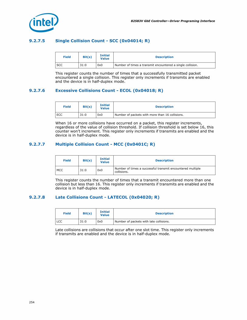
82583V GbE Controller—Driver Programing Interface
254
9.2.7.5 Single Collision Count - SCC (0x04014; R)
This register counts the number of times that a successfully transmitted packet encountered a single collision. This register only increments if transmits are enabled and the device is in half-duplex mode.
9.2.7.6 Excessive Collisions Count - ECOL (0x04018; R)
When 16 or more collisions have occurred on a packet, this register increments, regardless of the value of collision threshold. If collision threshold is set below 16, this counter won’t increment. This register only increments if transmits are enabled and the device is in half-duplex mode.
9.2.7.7 Multiple Collision Count - MCC (0x0401C; R)
This register counts the number of times that a transmit encountered more than one collision but less than 16. This register only increments if transmits are enabled and the device is in half-duplex mode.
9.2.7.8 Late Collisions Count - LATECOL (0x04020; R)
Late collisions are collisions that occur after one slot time. This register only increments if transmits are enabled and the device is in half-duplex mode.
Field Bit(s) Initial Value Description
SCC 31:0 0x0 Number of times a transmit encountered a single collision.
Field Bit(s) Initial Value Description
ECC 31:0 0x0 Number of packets with more than 16 collisions.
Field Bit(s) Initial Value Description
MCC 31:0 0x0 Number of times a successful transmit encountered multiple collisions.
Field Bit(s) Initial Value Description
LCC 31:0 0x0 Number of packets with late collisions.

255
Driver Programing Interface—82583V GbE Controller
9.2.7.9 Collision Count - COLC (0x04028; R)
This register counts the total number of collisions seen by the transmitter. This register only increments if transmits are enabled and the device is in half-duplex mode. This register applies to clear as well as secure traffic.
9.2.7.10 Defer Count - DC (0x04030; R)
This register counts defer events. A defer event occurs when the transmitter cannot immediately send a packet due to the medium being busy either because:
• Another device is transmitting• The IPG timer has not expired• Hhalf-duplex deferral events• Reception of XOFF frames• The link is not up
This register only increments if transmits are enabled. The behavior of this counter is slightly different in the 82583V relative to previous devices. For the 82583V, this counter does not increment for streaming transmits that are deferred due to TX IPG.
9.2.7.11 Transmit with No CRS - TNCRS (0x04034; R)
This register counts the number of successful packet transmissions in which the CRS input from the PHY was not asserted within one slot time of start of transmission from the MAC. Start of transmission is defined as the assertion of TX_EN to the PHY.
The PHY should assert CRS during every transmission. Failure to do so might indicate that the link has failed, or the PHY has an incorrect link configuration. This register only increments if transmits are enabled. This register is only valid when the 82583V is operating at half duplex.
Field Bit(s) Initial Value Description
COLC 31:0 0x0 Total number of collisions experienced by the transmitter.
Field Bit(s) Initial Value Description
CDC 31:0 0x0 Number of defer events.
Field Bit(s) Initial Value Description
TNCRS 31:0 0x0 Number of transmissions without a CRS assertion from the PHY.

82583V GbE Controller—Driver Programing Interface
256
9.2.7.12 Carrier Extension Error Count - CEXTERR (0x0403C; R)
This register counts the number of packets received in which the carrier extension error was signaled across the GMII interface. The PHY propagates carrier extension errors to the MAC when an error is detected during the carrier extended time of a packet reception. An extension error is signaled by the PHY by the encoding of 0x1F on the receive data inputs while RX_ER is asserted to the MAC. This register only increments if receives are enabled and the device is operating at 1000 Mb/s.
9.2.7.13 Receive Length Error Count - RLEC (0x04040; R)
This register counts receive length error events. A length error occurs if an incoming packet passes the filter criteria but is undersized or oversized. Packets less than 64 bytes are undersized. Packets over 1522 bytes are oversized if LongPacketEnable is 0b.
Note: The 82583V does not support setting LPE to 1b.
If receives are not enabled, this register does not increment. These lengths are based on bytes in the received packet from <Destination Address> through <CRC>, inclusively.
9.2.7.14 XON Received Count - XONRXC (0x04048; R)
This register counts the number of XON packets received. XON packets can use the global address, or the station address. This register only increments if receives are enabled.
9.2.7.15 XON Transmitted Count - XONTXC (0x0404C; R)
This register counts the number of XON packets transmitted. These can be either due to queue fullness, or due to software initiated action (using SWXOFF). This register only increments if transmits are enabled.
Field Bit(s) Initial Value Description
CEXTERR 31:0 0x0 Number of packets received with a carrier extension error.
Field Bit(s) Initial Value Description
RLEC 31:0 0x0 Number of packets with receive length errors.
Field Bit(s) Initial Value Description
XONRXC 31:0 0x0 Number of XON packets received.
Field Bit(s) Initial Value Description
XONTXC 31:0 0x0 Number of XON packets transmitted.

257
Driver Programing Interface—82583V GbE Controller
9.2.7.16 XOFF Received Count - XOFFRXC (0x04050; R)
This register counts the number of XOFF packets received. XOFF packets can use the global address, or the station address. This register only increments if receives are enabled.
9.2.7.17 XOFF Transmitted Count - XOFFTXC (0x04054; R)
This register counts the number of XOFF packets transmitted. These can be either due to queue fullness, or due to software initiated action (using SWXOFF). This register only increments if transmits are enabled.
9.2.7.18 FC Received Unsupported Count - FCRUC (0x04058; RW)
This register counts the number of unsupported flow control frames that are received.
The FCRUC counter is incremented when a flow control packet is received that matches either the reserved flow control multicast address (in FCAH/L) or the MAC station address, and has a matching flow control type field match (to the value in FCT), but has an incorrect op-code field. This register only increments if receives are enabled.
9.2.7.19 Packets Received [64 Bytes] Count - PRC64 (0x0405C; RW)
This register counts the number of good packets received that are exactly 64 bytes (from <Destination Address> through <CRC>, inclusively) in length. Packets that are counted in the Missed Packet Count register are not counted in this register. This register does not include received flow control packets and increments only if receives are enabled.
Field Bit(s) Initial Value Description
XOFFRXC 31:0 0x0 Number of XOFF packets received.
Field Bit(s) Initial Value Description
XOFFTXC 31:0 0x0 Number of XOFF packets transmitted.
Field Bit(s) Initial Value Description
FCRUC 31:0 0x0 Number of unsupported flow control frames received.
Field Bit(s) Initial Value Description
PRC64 31:0 0 Number of packets received that are 64 bytes in length.

82583V GbE Controller—Driver Programing Interface
258
9.2.7.20 Packets Received [65–127 Bytes] Count - PRC127 (0x04060; RW)
This register counts the number of good packets received that are 65-127 bytes (from <Destination Address> through <CRC>, inclusively) in length. Packets that are counted in the Missed Packet Count register are not counted in this register. This register does not include received flow control packets and increments only if receives are enabled.
9.2.7.21 Packets Received [128–255 Bytes] Count - PRC255 (0x04064; RW)
This register counts the number of good packets received that are 128-255 bytes (from <Destination Address> through <CRC>, inclusively) in length. Packets that are counted in the Missed Packet Count register are not counted in this register. This register does not include received flow control packets and increments only if receives are enabled.
9.2.7.22 Packets Received [256–511 Bytes] Count - PRC511 (0x04068; RW)
This register counts the number of good packets received that are 256-511 bytes (from <Destination Address> through <CRC>, inclusively) in length. Packets that are counted in the Missed Packet Count register are not counted in this register. This register does not include received flow control packets and increments only if receives are enabled.
9.2.7.23 Packets Received [512–1023 Bytes] Count - PRC1023 (0x0406C; RW)
This register counts the number of good packets received that are 512-1023 bytes (from <Destination Address> through <CRC>, inclusively) in length. Packets that are counted in the Missed Packet Count register are not counted in this register. This register does not include received flow control packets and increments only if receives are enabled.
Field Bit(s) Initial Value Description
PRC127 31:0 0x0 Number of packets received that are 65-127 bytes in length.
Field Bit(s) Initial Value Description
PRC255 31:0 0x0 Number of packets received that are 128-255 bytes in length.
Field Bit(s) Initial Value Description
PRC511 31:0 0x0 Number of packets received that are 256-511 bytes in length.
Field Bit(s) Initial Value Description
PRC1023 31:0 0x0 Number of packets received that are 512-1023 bytes in length.

259
Driver Programing Interface—82583V GbE Controller
9.2.7.24 Packets Received [1024 to Max Bytes] Count - PRC1522 (0x04070; RW)
This register counts the number of good packets received that are from 1024 bytes to the maximum (from <Destination Address> through <CRC>, inclusively) in length. The maximum is dependent on the current receiver configuration and the type of packet being received. If a packet is counted in the Receive Oversized Count register, it is not counted in this register (see Section 9.2.7.36). This register does not include received flow control packets and only increments if the packet has passed address filtering and receives are enabled.
Due to changes in the standard for maximum frame size for VLAN tagged frames in 802.3, this device accepts packets which have a maximum length of 1522 bytes. The RMON statistics associated with this range has been extended to count 1522 byte long packets.
9.2.7.25 Good Packets Received Count - GPRC (0x04074; R)
This register counts the number of good (non-erred) packets received of any legal length. The legal length for the received packet is defined by the value of LPE (see Section 9.2.7.13). This register does not include received flow control packets and only counts packets that pass filtering. This register only increments if receives are enabled. This register does not count packets counted by the Missed Packet Count (MPC) register.
9.2.7.26 Broadcast Packets Received Count - BPRC (0x04078; R)
This register counts the number of good (non-erred) broadcast packets received. This register does not count broadcast packets received when the broadcast address filter is disabled. This register only increments if receives are enabled.
Field Bit(s) Initial Value Description
PRC1522 31:0 0x0 Number of packets received that are 1024-maximum bytes in length.
Field Bit(s) Initial Value Description
GPRC 31:0 0x0 Number of good packets received (of any length).
Field Bit(s) Initial Value Description
BPRC 31:0 0x0 Number of broadcast packets received.

82583V GbE Controller—Driver Programing Interface
260
9.2.7.27 Multicast Packets Received Count - MPRC (0x0407C; R)
This register counts the number of good (non-erred) multicast packets received. This register does not count multicast packets received that fail to pass address filtering nor does it count received flow control packets. This register only increments if receives are enabled. This register does not count packets counted by the Missed Packet Count (MPC) register.
9.2.7.28 Good Packets Transmitted Count - GPTC (0x04080; R)
This register counts the number of good (non-erred) packets transmitted. A good transmit packet is considered one that is 64 or more bytes in length (from <Destination Address> through <CRC>, inclusively) in length. This does not include transmitted flow control packets. This register only increments if transmits are enabled. This register does not count packets counted by the Missed Packet Count (MPC) register. The register counts clear as well as secure packets.
9.2.7.29 Good Octets Received Count - GORCL (0x04088; R)
9.2.7.30 Good Octets Received Count - GORCH (0x0408C; R)
These registers make up a logical 64-bit register that counts the number of good (non-erred) octets received. This register includes bytes received in a packet from the <Destination Address> field through the <CRC> field, inclusively. This register must be accessed using two independent 32-bit accesses. This register resets whenever the upper 32 bits are read (GORCH).
In addition, it sticks at 0xFFFF_FFFF_FFFF_FFFF when the maximum value is reached. Only packets that pass address filtering are counted in this register. This register only increments if receives are enabled.
These octets do not include octets in received flow control packets.
Field Bit(s) Initial Value Description
MPRC 31:0 0x0 Number of multicast packets received.
Field Bit(s) Initial Value Description
GPTC 31:0 0x0 Number of good packets transmitted.
Field Bit(s) Initial Value Description
GORCL 31:0 0x0 Number of good octets received – lower 4 bytes.
GORCH 31:0 0x0 Number of good octets received – upper 4 bytes.
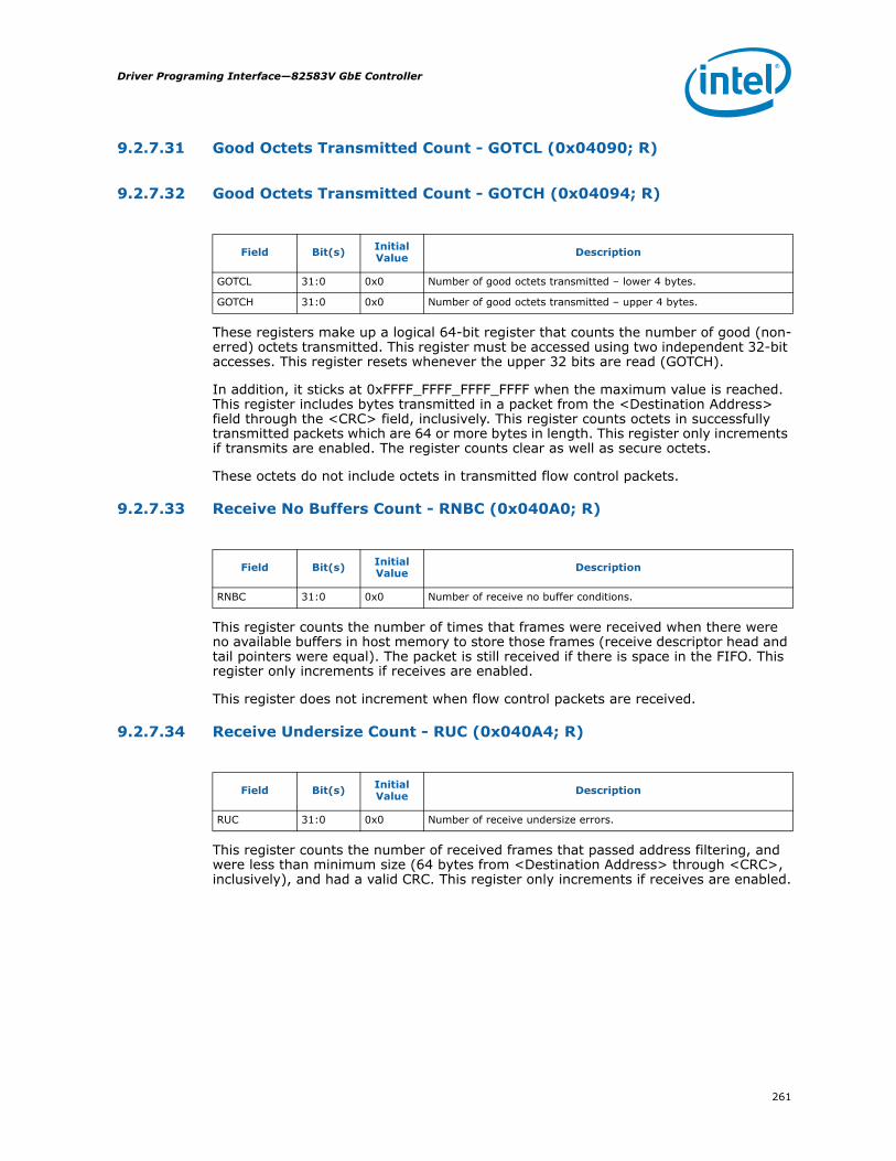
261
Driver Programing Interface—82583V GbE Controller
9.2.7.31 Good Octets Transmitted Count - GOTCL (0x04090; R)
9.2.7.32 Good Octets Transmitted Count - GOTCH (0x04094; R)
These registers make up a logical 64-bit register that counts the number of good (non-erred) octets transmitted. This register must be accessed using two independent 32-bit accesses. This register resets whenever the upper 32 bits are read (GOTCH).
In addition, it sticks at 0xFFFF_FFFF_FFFF_FFFF when the maximum value is reached. This register includes bytes transmitted in a packet from the <Destination Address> field through the <CRC> field, inclusively. This register counts octets in successfully transmitted packets which are 64 or more bytes in length. This register only increments if transmits are enabled. The register counts clear as well as secure octets.
These octets do not include octets in transmitted flow control packets.
9.2.7.33 Receive No Buffers Count - RNBC (0x040A0; R)
This register counts the number of times that frames were received when there were no available buffers in host memory to store those frames (receive descriptor head and tail pointers were equal). The packet is still received if there is space in the FIFO. This register only increments if receives are enabled.
This register does not increment when flow control packets are received.
9.2.7.34 Receive Undersize Count - RUC (0x040A4; R)
This register counts the number of received frames that passed address filtering, and were less than minimum size (64 bytes from <Destination Address> through <CRC>, inclusively), and had a valid CRC. This register only increments if receives are enabled.
Field Bit(s) Initial Value Description
GOTCL 31:0 0x0 Number of good octets transmitted – lower 4 bytes.
GOTCH 31:0 0x0 Number of good octets transmitted – upper 4 bytes.
Field Bit(s) Initial Value Description
RNBC 31:0 0x0 Number of receive no buffer conditions.
Field Bit(s) Initial Value Description
RUC 31:0 0x0 Number of receive undersize errors.

82583V GbE Controller—Driver Programing Interface
262
9.2.7.35 Receive Fragment Count - RFC (0x040A8; R)
This register counts the number of received frames that passed address filtering, and were less than minimum size (64 bytes from <Destination Address> through <CRC>, inclusively), but had a bad CRC (this is slightly different from the Receive Undersize Count register). This register only increments if receives are enabled.
9.2.7.36 Receive Oversize Count - ROC (0x040AC; R)
This register counts the number of received frames that passed address filtering, and were greater than maximum size. Packets over 1522 bytes are oversized if LPE is 0b.
Note: The 82583V does not support setting LPE to 1b.
If receives are not enabled, this register does not increment. These lengths are based on bytes in the received packet from <Destination Address> through <CRC>, inclusively.
9.2.7.37 Receive Jabber Count - RJC (0x040B0; R)
This register counts the number of received frames that passed address filtering, and were greater than maximum size and had a bad CRC (this is slightly different from the Receive Oversize Count register).
Packets over 1522 bytes are oversized if LPE is 0b.
Note: The 82583V does not support setting LPE to 1b.
If receives are not enabled, this register does not increment. These lengths are based on bytes in the received packet from <Destination Address> through <CRC>, inclusively.
Field Bit(s) Initial Value Description
RFC 31:0 0x0 Number of receive fragment errors.
Field Bit(s) Initial Value Description
ROC 31:0 0x0 Number of receive oversize errors.
Field Bit(s) Initial Value Description
RJC 31:0 0x0 Number of receive jabber errors.

263
Driver Programing Interface—82583V GbE Controller
9.2.7.38 Total Octets Received - TORL (0x040C0; R)
9.2.7.39 Total Octets Received - TORH (0x040C4; R)
These registers make up a logical 64-bit register that counts the total number of octets received. This register must be accessed using two independent 32-bit accesses. This register resets whenever the upper 32 bits are read (TORH). In addition, it sticks at 0xFFFF_FFFF_FFFF_FFFF when the maximum value is reached.
All packets received have their octets summed into this register, regardless of their length, whether they are erred, or whether they are flow control packets. This register includes bytes received in a packet from the <Destination Address> field through the <CRC> field, inclusively. This register only increments if receives are enabled.
Note: Broadcast rejected packets are counted in this counter (in contradiction to all other rejected packets that are not counted).
9.2.7.40 Total Octets Transmitted - TOT (0x040C8; RW)
These registers make up a logical 64-bit register that counts the total number of octets transmitted. This register must be accessed using two independent 32-bit accesses. This register resets whenever the upper 32 bits are read (TOTH). In addition, it sticks at 0xFFFF_FFFF_FFFF_FFFF when the maximum value is reached.
All transmitted packets have their octets summed into this register, regardless of their length or whether they are flow control packets. This register includes bytes transmitted in a packet from the <Destination Address> field through the <CRC> field, inclusively.
Octets transmitted as part of partial packet transmissions (for example, collisions in half-duplex mode) are not included in this register. This register only increments if transmits are enabled.
Field Bit(s) Initial Value Description
TORL 31:0 0x0 Number of total octets received – lower 4 bytes.
TORH 31:0 0x0 Number of total octets received – upper 4 bytes.
Field Bit(s) Initial Value Description
TOTL 31:0 0x0 Number of total octets transmitted – lower 4 bytes.
TOTH 31:0 0x0 Number of total octets transmitted – upper 4 bytes.

82583V GbE Controller—Driver Programing Interface
264
9.2.7.41 Total Packets Received - TPR (0x040D0; RW)
This register counts the total number of all packets received. All packets received are counted in this register, regardless of their length, whether they are erred, or whether they are flow control packets. This register only increments if receives are enabled.
Note: Broadcast rejected packets are counted in this counter (in contradiction to all other rejected packets that are not counted).
9.2.7.42 Total Packets Transmitted - TPT (0x040D4; RW)
This register counts the total number of all packets transmitted. All packets transmitted will be counted in this register, regardless of their length, or whether they are flow control packets.
Partial packet transmissions (for example, collisions in half-duplex mode) are not included in this register. This register only increments if transmits are enabled. This register counts all packets, including standard packets and secure packets.
9.2.7.43 Packets Transmitted [64 Bytes] Count - PTC64 (0x040D8; RW)
This register counts the number of packets transmitted that are exactly 64 bytes (from <Destination Address> through <CRC>, inclusively) in length. Partial packet transmissions (for example, collisions in half-duplex mode) are not included in this register. This register does not include transmitted flow control packets (which are 64 bytes in length). This register only increments if transmits are enabled. This register counts all packets, including standard packets and secure packets.
9.2.7.44 Packets Transmitted [65–127 Bytes] Count- PTC127 (0x040DC; RW)
This register counts the number of packets transmitted that are 65-127 bytes (from <Destination Address> through <CRC>, inclusively) in length. Partial packet transmissions (for example, collisions in half-duplex mode) are not included in this register. This register only increments if transmits are enabled. This register counts all packets, including standard packets and secure packets.
Field Bit(s) Initial Value Description
TPR 31:0 0x0 Number of all packets received.
Field Bit(s) Initial Value Description
TPT 31:0 0x0 Number of all packets transmitted.
Field Bit(s) Initial Value Description
PTC64 31:0 0x0 Number of packets transmitted that are 64 bytes in length.
Field Bit(s) Initial Value Description
PTC127 31:0 0x0 Number of packets transmitted that are 65-127 bytes in length.

265
Driver Programing Interface—82583V GbE Controller
9.2.7.45 Packets Transmitted [128–255 Bytes] Count - PTC255 (0x040E0; RW)
This register counts the number of packets transmitted that are 128-255 bytes (from <Destination Address> through <CRC>, inclusively) in length. Partial packet transmissions (for example, collisions in half-duplex mode) are not included in this register. This register only increments if transmits are enabled. This register counts all packets, including standard packets and secure packets.
9.2.7.46 Packets Transmitted [256–511 Bytes] Count - PTC511 (0x040E4; RW)
This register counts the number of packets transmitted that are 256-511 bytes (from <Destination Address> through <CRC>, inclusively) in length. Partial packet transmissions (for example, collisions in half-duplex mode) are not included in this register. This register only increments if transmits are enabled. This register counts all packets, including standard and secure packets.
9.2.7.47 Packets Transmitted [512–1023 Bytes] Count - PTC1023 (0x040E8; RW)
This register counts the number of packets transmitted that are 512-1023 bytes (from <Destination Address> through <CRC>, inclusively) in length. Partial packet transmissions (for example, collisions in half-duplex mode) are not included in this register. This register only increments if transmits are enabled. This register counts all packets, including standard and secure packets.
9.2.7.48 Packets Transmitted [Greater than 1024 Bytes] Count - PTC1522 (0x040EC; RW)
This register counts the number of packets transmitted that are 1024 or more bytes (from <Destination Address> through <CRC>, inclusively) in length. Partial packet transmissions (for example, collisions in half-duplex mode) are not included in this register. This register only increments if transmits are enabled.
Field Bit(s) Initial Value Description
PTC255 31:0 0x0 Number of packets transmitted that are 128-255 bytes in length.
Field Bit(s) Initial Value Description
PTC511 31:0 0x0 Number of packets transmitted that are 256-511 bytes in length.
Field Bit(s) Initial Value Description
PTC1023 31:0 0x0 Number of packets transmitted that are 512-1023 bytes in length.
Field Bit(s) Initial Value Description
PTC1522 31:0 0x0 Number of packets transmitted that are 1024 or more bytes in length.

82583V GbE Controller—Driver Programing Interface
266
Due to changes in the standard for maximum frame size for VLAN tagged frames in 802.3, this device transmits packets that have a maximum length of 1522 bytes. The RMON statistics associated with this range has been extended to count 1522 byte long packets. This register counts all packets, including standard and secure packets.
9.2.7.49 Multicast Packets Transmitted Count - MPTC (0x040F0; RW)
This register counts the number of multicast packets transmitted. This register does not include flow control packets and increments only if transmits are enabled. Counts clear as well as secure traffic.
9.2.7.50 Broadcast Packets Transmitted Count - BPTC (0x040F4; RW)
This register counts the number of broadcast packets transmitted. This register only increments if transmits are enabled. This register counts all packets, including standard and secure packets.
9.2.7.51 TCP Segmentation Context Transmitted Count - TSCTC (0x040F8; RW)
This register counts the number of TCP segmentation offload transmissions and increments once the last portion of the TCP segmentation context payload is segmented and loaded as a packet into the on-chip transmit buffer. Note that it is not a measurement of the number of packets sent out (covered by other registers). This register only increments if transmits and TCP segmentation offload are enabled.
9.2.7.52 TCP Segmentation Context Transmit Fail Count - TSCTFC (0x040FC; RW)
This register counts the number of TCP segmentation offload requests to the hardware that failed to transmit all data in the TCP segmentation context payload. There is no indication by hardware of how much data was successfully transmitted. Only one failure event is logged per TCP segmentation context. Failures could be due to Paylen errors. This register will only increment if transmits are enabled.
Field Bit(s) Initial Value Description
MPTC 31:0 0x0 Number of multicast packets transmitted.
Field Bit(s) Initial Value Description
BPTC 31:0 0x0 Number of broadcast packets transmitted count.
Field Bit(s) Initial Value Description
TSCTC 31:0 0x0 Number of TCP Segmentation contexts transmitted count.
Field Bit(s) Initial Value Description
TSCTFC 31:0 0x0 Number of TCP segmentation contexts where the device failed to transmit the entire data payload.
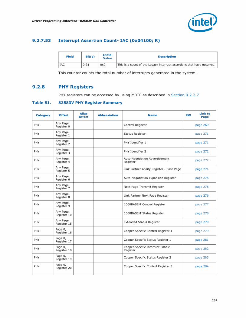
267
Driver Programing Interface—82583V GbE Controller
9.2.7.53 Interrupt Assertion Count- IAC (0x04100; R)
This counter counts the total number of interrupts generated in the system.
9.2.8 PHY Registers
PHY registers can be accessed by using MDIC as described in Section 9.2.2.7
Table 51. 82583V PHY Register Summary
Field Bit(s) Initial Value Description
IAC 0-31 0x0 This is a count of the Legacy interrupt assertions that have occurred.
Category Offset Alias Offset Abbreviation Name RW Link to
Page
PHY Any Page, Register 0 Control Register page 269
PHY Any Page, Register 1 Status Register page 271
PHY Any Page, Register 2 PHY Identifier 1 page 271
PHY Any Page, Register 3 PHY Identifier 2 page 272
PHY Any Page, Register 4
Auto-Negotiation Advertisement Register page 272
PHY Any Page, Register 5 Link Partner Ability Register - Base Page page 274
PHY Any Page, Register 6 Auto-Negotiation Expansion Register page 275
PHY Any Page, Register 7 Next Page Transmit Register page 276
PHY Any Page, Register 8 Link Partner Next Page Register page 276
PHY Any Page, Register 9 1000BASE-T Control Register page 277
PHY Any Page, Register 10 1000BASE-T Status Register page 278
PHY Any Page, Register 15 Extended Status Register page 279
PHY Page 0, Register 16 Copper Specific Control Register 1 page 279
PHY Page 0, Register 17 Copper Specific Status Register 1 page 281
PHY Page 0, Register 18
Copper Specific Interrupt Enable Register page 282
PHY Page 0, Register 19 Copper Specific Status Register 2 page 283
PHY Page 0, Register 20 Copper Specific Control Register 3 page 284

82583V GbE Controller—Driver Programing Interface
268
Category Offset Alias Offset Abbreviation Name RW Link to
Page
PHY Page 0, Register 21 Receive Error Counter Register page 284
PHY Any Page, Register 22 Page Address page 285
PHY Page 0, Register 25 OEM Bits page 285
PHY Page 0, Register 26 Copper Specific Control Register 2 page 286
PHY Page 0, Register 29 Bias Setting Register 1 page 287
PHY Page 0, Register 30 Bias Setting Register 2 page 287
PHY Page 2, Register 16 MAC Specific Control Register 1 page 287
PHY Page 2, Register 18 MAC Specific Interrupt Enable Register page 288
PHY Page 2, Register 19 MAC Specific Status Register page 288
PHY Page 2, Register 21 MAC Specific Control Register 2 page 289
PHY Page 3, Register 16 LED[3:0] Function Control Register page 289
PHY Page 3, Register 17 LED[3:0] Polarity Control Register page 292
PHY Page 3, Register 18 LED Timer Control Register page 293
PHY Page 3, Register 19
LED[5:4] Function Control and Polarity Register page 294
PHY Page 5, Register 20 1000 BASE-T Pair Skew Register page 295
PHY Page 5, Register 21 1000 BASE-T Pair Swap and Polarity page 295
PHY Page 6, Register 17 CRC Counters page 295

269
Driver Programing Interface—82583V GbE Controller
9.2.8.1 Control Register (Any Page), PHY Address 01; Register 0
Bits Field Mode HW Rst SW Rst Description
15 Reset R/W, SC 0x0 SC
PHY Software Reset. Writing a 1b to this bit causes the PHY state machines to be reset. When the reset operation completes, this bit is automatically cleared to 0b. The reset occurs immediately.1b = PHY reset.0b = Normal operation.
14 Loopback R/W 0x0 0x0
When loopback is activated, the transmitter data presented on TXD is looped back to RXD internally. The link is broken when loopback is enabled. Loopback speed is determined by registers 21_2.2:0. 1b = Enable loopback.0b = Disable loopback.
13 Speed Select (LSB) R/W 0x0 Update
Changes to this bit are disruptive to the normal operation; therefore, any changes to these registers must be followed by a software reset to take effect. A write to this register bit does not take effect until any one of the following also occurs: • Software reset is asserted (register 0.15).• Restart auto-negotiation is asserted (register
0.9).• Power down (register 0.11, 16_0.2) transitions
from power down to normal operation (bit 6, 13).
11b = Reserved.10b = 1000 Mb/s.01b = 100 Mb/s.00b = 10 Mb/s.
12Auto-Negotiation Enable
R/W 0x1 Update
Changes to this bit are disruptive to the normal operation. A write to this register bit does not take effect until any one of the following occurs: • Software reset is asserted (register 0.15).• Restart auto-negotiation is asserted (register
0.9).• Power down (register 0.11, 16_0.2) transitions
from power down to normal operation.If register 0.12 is set to 0b and speed is manually forced to 1000 Mb/s in registers 0.13 and 0.6, then auto- negotiation is still enabled and only 1000BASE-T full-duplex is advertised if register 0.8 is set to 1b, and 1000BASE-T half-duplex is advertised if register 0.8 is set to 0b. Registers 4.8:5 and 9.9:8 are ignored. Auto-negotiation is mandatory per IEEE for proper operation in 1000BASE-T. 1b = Enable auto-negotiation process.0b = Disable auto-negotiation process.

82583V GbE Controller—Driver Programing Interface
270
11 Power Down R/W See Description Retain
Power down is controlled via register 0.11 and 16_0.2. Both bits must be set to 0b before the PHY transitions from power down to normal operation. When the port is switched from power down to normal operation, a software reset and restart auto-negotiation are performed even when bits Reset (0_15) and Restart Auto-Negotiation (0.9) are not set by the user. IEEE power down shuts down the 82583V except for the GMII interface if 16_2.3 is set to 1b. If 16_2.3 is set to 0b, then the GMII interface also shuts down. After a hardware reset, this bit takes on the value of pd_pwrdn_a.1b = Power down.0b = Normal operation.When pd_pwrdn_a transitions from 1b to 0b this bit is set to 0b. When pd_pwrdn_a transitions from 0b to 1b this bit is set to 1b.
10 Isolate RO 0x0 0x0 This bit has no effect.
9
Restart Copper Auto-Negotiation
R/W,SC 0x0 SC
When pd_aneg_now_a transitions from 0b to 1b this bit is set to 1b. Auto-negotiation automatically restarts after hardware or software reset regardless of whether or not the Restart bit (0.9) is set. 1b = Restart auto-negotiation process.0b = Normal operation.
8Copper Duplex Mode
R/W 0x1 Update
Changes to this bit are disruptive to the normal operation; therefore, any changes to these registers must be followed by a software reset to take effect. A write to this register bit does not take effect until any one of the following also occurs: • Software reset is asserted (register 0.15).• Restart auto-negotiation is asserted (register
0.9).• Power down (register 0.11, 16_0.2) transitions
from power down to normal operation.1b = Full-duplex.0b = Half-duplex.
7 Collision Test RO 0x0 0x0 This bit has no effect.
6Speed Selection (MSB)
R/W 0x1 Update
Changes to this bit are disruptive to the normal operation; therefore, any changes to these registers must be followed by a software reset to take effect. A write to this register bit does not take effect until any one of the following occurs: • Software reset is asserted (register 0.15).• Restart auto-negotiation is asserted (register
0.9).• Power down (register 0.11, 16_0.2) transitions
from power down to normal operation (bit 6, 13).
11b = Reserved.10b = 1000 Mb/s.01b = 100 Mb/s.00b = 10 Mb/s.
5:0 Reserved RO Always 0x0 Always 0x0 Reserved, always 0x0.
Bits Field Mode HW Rst SW Rst Description

271
Driver Programing Interface—82583V GbE Controller
9.2.8.2 Status Register (Any Page), PHY Address 01; Register 1
9.2.8.3 PHY Identifier 1 (Any Page), PHY Address 01; Register 2
Bits Field Mode HW Rst SW Rst Description
15 100BASE-T4 RO Always 0b
Always 0b
100BASE-T4. This protocol is not available.0b = PHY not able to perform 100BASE-T4.
14 100BASE-X Full-Duplex RO Always
1bAlways 1b 1b = PHY able to perform full-duplex 100BASE-X.
13 100BASE-X Half-Duplex RO Always
1bAlways 1b 1b = PHY able to perform half-duplex 100BASE-X.
12 10 Mbps Full- Duplex RO Always
1bAlways 1b 1b = PHY able to perform full-duplex 10BASE-T.
11 10 Mbps Half-Duplex RO Always
1bAlways 1b 1b = PHY able to perform half-duplex 10BASE-T.
10 100BASE-T2 Full-Duplex RO Always
0bAlways 0b
This protocol is not available.0b = PHY not able to perform full-duplex.
9 100BASE-T2 Half-Duplex RO Always
0bAlways 0b
This protocol is not available.0b = PHY not able to perform half-duplex.
8 Extended Status RO Always 1b
Always 1b 1b = Extended status information in register 15.
7 Reserved RO Always 0b
Always 0b Reserved, always 0b.
6 MF Preamble Suppression RO Always
1bAlways 1b
1b = PHY accepts management frames with preamble suppressed.
5Copper Auto- Negotiation Complete
RO 0x0 0x01b = Auto-negotiation process complete.0b = Auto-negotiation process not complete.
4 Copper Remote Fault
RO, LH 0x0 0x0
1b = Remote fault condition detected.0b = Remote fault condition not detected.
3Auto-Negotiation Ability
RO Always 1b
Always 1b 1b = PHY able to perform auto-negotiation.
2 Copper Link Status
RO, LL 0x0 0x0
This register bit indicates when link was LED[3] since the last read. For the current link status, either read this register back-to-back or read register 17_0.10 Link Real Time. 1b = Link is up.0b = Link is down.
1 Jabber Detect RO, LH 0x0 0x0
1b = Jabber condition detected.0b = Jabber condition not detected.
0 Extended Capability RO Always
1bAlways 1b 1b = Extended register capabilities.
Bits Field Mode HW Rst SW Rst Description
15:0Organizationally Unique Identifier Bit 3:18
RO 0x0141 0x0141
0x005043 0000 0000 0101 0000 0100 0011^ ^ bit 1....................................bit 24 register 2. [15:0] show bits 3 to 18 of the OUI. 0000000101000001 ^ ^ bit 3...................bit18

82583V GbE Controller—Driver Programing Interface
272
9.2.8.4 PHY Identifier 2 (Any Page), PHY Address 01; Register 3
9.2.8.5 Auto-Negotiation Advertisement Register (Any Page), PHY Address 01; Register 4
Bits Field Mode HW Rst SW Rst Description
15:10 OUI LSB RO Always 000011b 0x00 Organizationally Unique Identifier bits 19:24 00 0011 ^.........^ bit 19...bit 24
9:4 Model Number RO Always 001011b 0x00 Model Number 001011b.
3:0 Revision Number RO See Description See
Description
Rev Number.Contact FAEs for information on the device revision number.
Bits Field Mode HW Rst SW Rst Description
15 Next Page R/W 0x0 Update
A write to this register bit does not take effect until any one of the following occurs: • Software reset is asserted (register 0.15).• Restart auto-negotiation is asserted (register
0.9).• Power down (register 0.11, 16_0.2) transitions
from power down to normal operation.• Copper link goes down.
If 1000BASE-T is advertised then the required next pages are automatically transmitted. Register 4.15 should be set to 0b if no additional next pages are needed.1b = Advertise.0b = Not advertised.
14 Ack RO Always 0b Always 0b Reserved, must be 0b.
13 Remote Fault R/W 0x0 Update
A write to this register bit does not take effect until any one of the following occurs: • Software reset is asserted (register 0.15).• Restart auto-negotiation is asserted (register
0.9).• Power down (register 0.11, 16_0.2) transitions
from power down to normal operation.• Copper link goes down.
1b = Set Remote Fault bit.0b = Do not set Remote Fault bit.
12 Reserved R/W 0x0 Update
A write to this register bit does not take effect until any one of the following occurs: • Software reset is asserted (register 0.15).• Restart auto-negotiation is asserted (register
0.9).• Power down (register 0.11, 16_0.2) transitions
from power down to normal operation.• Copper link goes down.
Reserved bit is R/W to allow for forward compatibility with future IEEE standards.

273
Driver Programing Interface—82583V GbE Controller
11 Asymmetric Pause R/W See
Description Update
A write to this register bit does not take effect until any one of the following occurs: • Software reset is asserted (register 0.15).• Restart auto-negotiation is asserted (register
0.9).• Power down (register 0.11, 16_0.2) transitions
from power down to normal operation.• Copper link goes down.
After a hardware reset, this bit takes on the value of pd_config_asm_pause_a.1b = Asymmetric pause.0b = No asymmetric pause.
10 Pause R/W See Description Update
A write to this register bit does not take effect until any one of the following occurs: • Software reset is asserted (register 0.15).• Restart auto-negotiation is asserted (register
0.9).• Power down (register 0.11, 16_0.2) transitions
from power down to normal operation.• Copper link goes down.
After a hardware reset, this bit takes on the value of pd_config_pause_a.1b = MAC pause implemented.0b = MAC pause not implemented.
9 100BASE-T4 R/W 0x0 Retain 0b = Not capable of 100BASE-T4.
8 100BASE-TX Full-Duplex R/W 0x1 Update
A write to this register bit does not take effect until any one of the following occurs: • Software reset is asserted (register 0.15).• Restart auto-negotiation is asserted (register
0.9).• Power down (register 0.11, 16_0.2) transitions
from power down to normal operation.• Copper link goes down.
If register 0.12 is set to 0b and speed is manually forced to 1000 Mb/s in registers 0.13 and 0.6, then auto-negotiation is still enabled and only 1000BASE-T full-duplex is advertised if register 0.8 is set to 1b; 1000BASE-T half-duplex is advertised if 0.8 is set to 0b. Registers 4.8:5 and 9.9:8 are ignored. Auto-negotiation is mandatory per IEEE for proper operation in 1000BASE-T. 1b = Advertise.0b = Not advertised.
7 100BASE-TX Half-Duplex R/W 0x1 Update
A write to this register bit does not take effect until any one of the following occurs: • Software reset is asserted (register 0.15)• Restart auto-negotiation is asserted (register
0.9)• Power down (register 0.11, 16_0.2) transitions
from power down to normal operation• Copper link goes down.
If register 0.12 is set to 0b and speed is manually forced to 1000 Mb/s in registers 0.13 and 0.6, then auto-negotiation is still enabled and only 1000BASE-T full-duplex is advertised if register 0.8 is set to 1b; 1000BASE-T half-duplex is advertised if 0.8 is set to 0b. Registers 4.8:5 and 9.9:8 are ignored. Auto-negotiation is mandatory per IEEE for proper operation in 1000BASE-T.1b = Advertise.0b = Not advertised.
Bits Field Mode HW Rst SW Rst Description
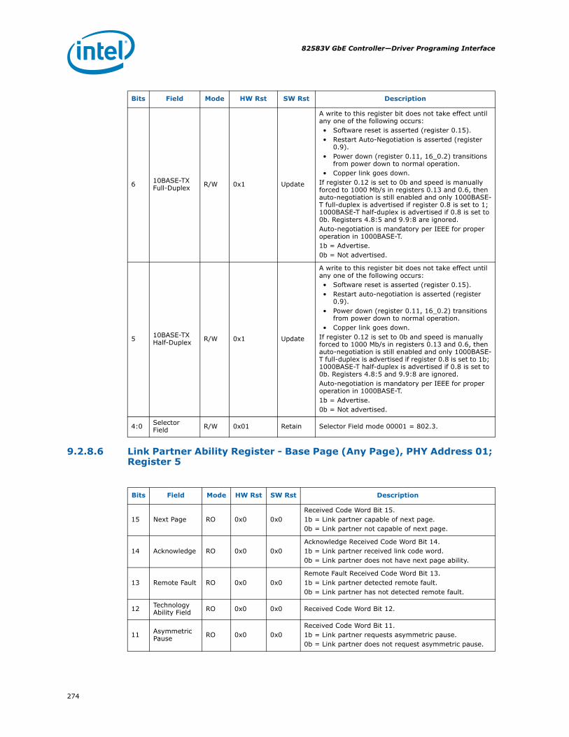
82583V GbE Controller—Driver Programing Interface
274
9.2.8.6 Link Partner Ability Register - Base Page (Any Page), PHY Address 01; Register 5
6 10BASE-TX Full-Duplex R/W 0x1 Update
A write to this register bit does not take effect until any one of the following occurs: • Software reset is asserted (register 0.15).• Restart Auto-Negotiation is asserted (register
0.9).• Power down (register 0.11, 16_0.2) transitions
from power down to normal operation.• Copper link goes down.
If register 0.12 is set to 0b and speed is manually forced to 1000 Mb/s in registers 0.13 and 0.6, then auto-negotiation is still enabled and only 1000BASE-T full-duplex is advertised if register 0.8 is set to 1; 1000BASE-T half-duplex is advertised if 0.8 is set to 0b. Registers 4.8:5 and 9.9:8 are ignored. Auto-negotiation is mandatory per IEEE for proper operation in 1000BASE-T. 1b = Advertise.0b = Not advertised.
5 10BASE-TX Half-Duplex R/W 0x1 Update
A write to this register bit does not take effect until any one of the following occurs: • Software reset is asserted (register 0.15).• Restart auto-negotiation is asserted (register
0.9).• Power down (register 0.11, 16_0.2) transitions
from power down to normal operation.• Copper link goes down.
If register 0.12 is set to 0b and speed is manually forced to 1000 Mb/s in registers 0.13 and 0.6, then auto-negotiation is still enabled and only 1000BASE-T full-duplex is advertised if register 0.8 is set to 1b; 1000BASE-T half-duplex is advertised if 0.8 is set to 0b. Registers 4.8:5 and 9.9:8 are ignored. Auto-negotiation is mandatory per IEEE for proper operation in 1000BASE-T. 1b = Advertise.0b = Not advertised.
4:0 Selector Field R/W 0x01 Retain Selector Field mode 00001 = 802.3.
Bits Field Mode HW Rst SW Rst Description
15 Next Page RO 0x0 0x0Received Code Word Bit 15.1b = Link partner capable of next page.0b = Link partner not capable of next page.
14 Acknowledge RO 0x0 0x0Acknowledge Received Code Word Bit 14.1b = Link partner received link code word.0b = Link partner does not have next page ability.
13 Remote Fault RO 0x0 0x0Remote Fault Received Code Word Bit 13.1b = Link partner detected remote fault.0b = Link partner has not detected remote fault.
12 Technology Ability Field RO 0x0 0x0 Received Code Word Bit 12.
11 Asymmetric Pause RO 0x0 0x0
Received Code Word Bit 11.1b = Link partner requests asymmetric pause.0b = Link partner does not request asymmetric pause.
Bits Field Mode HW Rst SW Rst Description

275
Driver Programing Interface—82583V GbE Controller
9.2.8.7 Auto-Negotiation Expansion Register (Any Page), PHY Address 01; Register 6
10 Pause Capable RO 0x0 0x0
Received Code Word Bit 10.1b = Link partner is capable of pause operation.0b = Link partner is not capable of pause operation.
9 100BASE-T4 Capability RO 0x0 0x0
Received Code Word Bit 9.1b = Link partner is 100BASE-T4 capable.0b = Link partner is not 100BASE-T4 capable.
8100BASE-TX Full-Duplex Capability
RO 0x0 0x0Received Code Word Bit 8.1b = Link partner is 100BASE-TX full-duplex capable.0b = Link partner is not 100BASE-TX full-duplex capable.
7100BASE-TX Half-Duplex Capability
RO 0x0 0x0
Received Code Word Bit 7.1b = Link partner is 100BASE-TX half-duplex capable.0b = Link partner is not 100BASE-TX half-duplex capable.
610BASE-T Full-Duplex Capability
RO 0x0 0x0Received Code Word Bit 6.1b = Link partner is 10BASE-T full-duplex capable.0b = Link partner is not 10BASE-T full-duplex capable.
510BASE-T Half-Duplex Capability
RO 0x0 0x0Received Code Word Bit 5.1b = Link partner is 10BASE-T half-duplex capable.0b = Link partner is not 10BASE-T half-duplex capable.
4:0 Selector Field RO 0x00 0x00 Selector Field Received Code Word Bit 4:0.
Bits Field Mode HW Rst SW Rst Description
15:5 Reserved RO 0x000 0x000 Reserved. Must be 00000000000.
4 Parallel Detection Fault RO,LH 0x0 0x0
Register 6.4 is not valid until the auto-negotiation complete bit (Reg 1.5) indicates completed.1b = A fault has been detected via the parallel detection function.0b = A fault has not been detected via the parallel detection function.
3 Link Partner Next page Able RO 0x0 0x0
Register 6.3 is not valid until the auto-negotiation complete bit (Reg 1.5) indicates completed.1b = Link partner is next page able.0b = Link partner is not next page able.
2 Local Next Page Able RO 0x1 0x1
Register 6.2 is not valid until the auto-negotiation complete bit (Reg 1.5) indicates completed.1b = Local device is next page able.0b = Local device is not next page able.
1 Page Received RO, LH 0x0 0x0
Register 6.1 is not valid until the auto-negotiation complete bit (Reg 1.5) indicates completed.1b = A new page has been received.0b = A new page has not been received.
0
Link Partner Auto- Negotiation Able
RO 0x0 0x0
Register 6.0 is not valid until the auto-negotiation complete bit (Reg 1.5) indicates completed.1b = Link partner is auto-negotiation able.0b = Link partner is not auto-negotiation able.
Bits Field Mode HW Rst SW Rst Description

82583V GbE Controller—Driver Programing Interface
276
9.2.8.8 Next Page Transmit Register (Any Page), PHY Address 01; Register 7
9.2.8.9 Link Partner Next Page Register (Any Page), PHY Address 01; Register 8
Bits Field Mode HW Rst SW Rst Description
15 Next Page R/W 0x0 0x0
Transmit Code Word Bit 15.A write to register 7 implicitly sets a variable in the auto-negotiation state machine indicating that the next page has been loaded. A link failure clears register 7.
14 Reserved RO 0x0 0x0 Transmit Code Word Bit 14.
13 Message Page Mode R/W 0x1 0x1 Transmit Code Word Bit 13.
12 Acknowledge2 R/W 0x0 0x0 Transmit Code Word Bit 12.
11 Toggle RO 0x0 0x0 Transmit Code Word Bit 11.
10:0Message/ Unformatted Field
R/W 0x001 0x001 Transmit Code Word Bit 10:0.
Bits Field Mode HW Rst SW Rst Description
15 Next Page RO 0x0 0x0 Received Code Word Bit 15.
14 Acknowledge RO 0x0 0x0 Received Code Word Bit 14.
13 Message Page RO 0x0 0x0 Received Code Word Bit 13.
12 Acknowledge2 RO 0x0 0x0 Received Code Word Bit 12.
11 Toggle RO 0x0 0x0 Received Code Word Bit 11.
10:0 Message Unformatted Field RO 0x000 0x000 Received Code Word Bit 10:0.
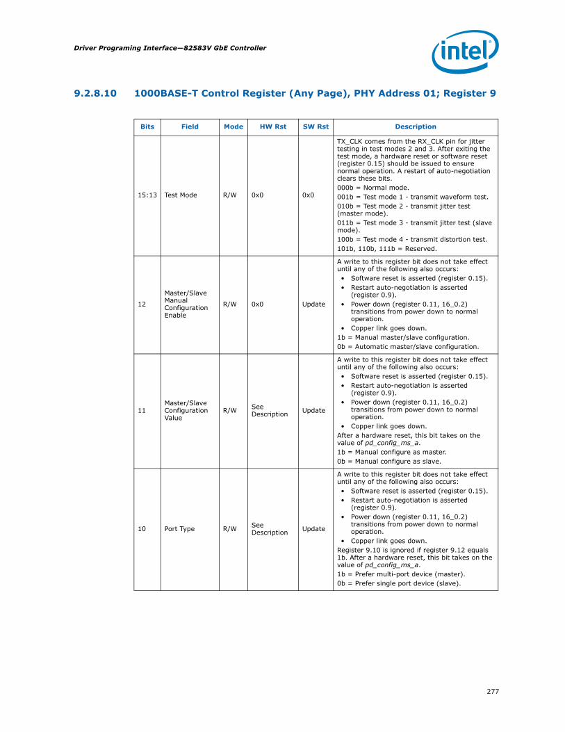
277
Driver Programing Interface—82583V GbE Controller
9.2.8.10 1000BASE-T Control Register (Any Page), PHY Address 01; Register 9
Bits Field Mode HW Rst SW Rst Description
15:13 Test Mode R/W 0x0 0x0
TX_CLK comes from the RX_CLK pin for jitter testing in test modes 2 and 3. After exiting the test mode, a hardware reset or software reset (register 0.15) should be issued to ensure normal operation. A restart of auto-negotiation clears these bits.000b = Normal mode.001b = Test mode 1 - transmit waveform test.010b = Test mode 2 - transmit jitter test (master mode).011b = Test mode 3 - transmit jitter test (slave mode).100b = Test mode 4 - transmit distortion test.101b, 110b, 111b = Reserved.
12
Master/Slave Manual Configuration Enable
R/W 0x0 Update
A write to this register bit does not take effect until any of the following also occurs: • Software reset is asserted (register 0.15).• Restart auto-negotiation is asserted
(register 0.9).• Power down (register 0.11, 16_0.2)
transitions from power down to normal operation.
• Copper link goes down. 1b = Manual master/slave configuration.0b = Automatic master/slave configuration.
11Master/Slave Configuration Value
R/W See Description Update
A write to this register bit does not take effect until any of the following also occurs: • Software reset is asserted (register 0.15).• Restart auto-negotiation is asserted
(register 0.9).• Power down (register 0.11, 16_0.2)
transitions from power down to normal operation.
• Copper link goes down. After a hardware reset, this bit takes on the value of pd_config_ms_a.1b = Manual configure as master.0b = Manual configure as slave.
10 Port Type R/W See Description Update
A write to this register bit does not take effect until any of the following also occurs: • Software reset is asserted (register 0.15).• Restart auto-negotiation is asserted
(register 0.9).• Power down (register 0.11, 16_0.2)
transitions from power down to normal operation.
• Copper link goes down. Register 9.10 is ignored if register 9.12 equals 1b. After a hardware reset, this bit takes on the value of pd_config_ms_a.1b = Prefer multi-port device (master).0b = Prefer single port device (slave).

82583V GbE Controller—Driver Programing Interface
278
9.2.8.11 1000BASE-T Status Register (Any Page), PHY Address 01; Register 10
9 1000BASE-T Full-Duplex R/W 0x1 Update
A write to this register bit does not take effect until any of the following also occurs: • Software reset is asserted (register 0.15).• Restart auto-negotiation is asserted
(register 0.9).• Power down (register 0.11, 16_0.2)
transitions from power down to normal operation.
• Copper link goes down. 1b = Advertise.0b = Not advertised.
8 1000BASE-T Half-Duplex R/W See
Description Update
A write to this register bit does not take effect until any of the following also occurs: • Software reset is asserted (register 0.15).• Restart auto-negotiation is asserted
(register 0.9).• Power down (register 0.11, 16_0.2)
transitions from power down to normal operation.
• Copper link goes down. After a hardware reset, this bit takes on the value of pd_config_1000hd_a.1 = Advertise.0 = Not advertised.
7:0 Reserved R/W 0x00 Retain Reserved, set to 0x00.
Bits Field Mode HW Rst SW Rst Description
15Master/Slave Configuration Fault
RO, LH 0x0 0x0
This register bit clears on reads.1b = master/slave configuration fault detected.0 = No master/slave configuration fault detected.
14Master/Slave Configuration Resolution
RO 0x0 0x01b = Local PHY configuration resolved to master.0b = Local PHY configuration resolved to slave.
13 Local Receiver Status RO 0x0 0x0
1b = Local receiver operational.0b = Local receiver is not operational.
12Remote Receiver Status
RO 0x0 0x01b = Remote receiver operational.0b = Remote receiver not operational.
11
Link Partner 1000BASE-T Full-Duplex Capability
RO 0x0 0x0
1b = Link partner is capable of 1000BASE-T full-duplex.0b = Link partner is not capable of 1000BASE-T full duplex.
10
Link Partner 1000BASE-T Half-Duplex Capability
RO 0x0 0x0
1b = Link partner is capable of 1000BASE-T half-duplex.0b = Link partner is not capable of 1000BASE-T half duplex.
9:8 Reserved RO 0x0 0x0 Reserved.
7:0 Idle Error Count
RO, SC 0x00 0x00
MSB of Idle Error Counter.These register bits report the idle error count since the last time this register was read. The counter reaches its maximum at 11111111b and does not roll over.
Bits Field Mode HW Rst SW Rst Description

279
Driver Programing Interface—82583V GbE Controller
9.2.8.12 Extended Status Register (Any Page), PHY Address 01; Register 15
9.2.8.13 Copper Specific Control Register 1 (Page 0), PHY Address 01; Register 16
Bits Field Mode HW Rst SW Rst Description
15 1000BASE-X Full-Duplex RO Always 0b Always 0b 0b = Not 1000BASE-X full-duplex capable.
14 1000BASE-X Half-Duplex RO Always 0b Always 0b 0b = Not 1000BASE-X half-duplex capable.
13 1000BASE-T Full-Duplex RO Always 1b Always 1b 1b =1000BASE-T full-duplex capable.
12 1000BASE-T Half-Duplex RO Always 1b Always 1b 1b =1000BASE-T half-duplex capable.
11:0 Reserved RO 0x000 0x000 Reserved, set to 0x000.
Bits Field Mode HW Rst SW Rst Description
15 Disable Link Pulses R/W 0x0 0x0
1b = Disable link pulse.0b = Enable link pulse.
14:12 Downshift Counter R/W 0x3 Update
Changes to these bits are disruptive to the normal operation; therefore, any changes to these registers must be followed by software reset to take effect. 1x, 2x,...8x is the number of times the PHY attempts to establish GbE link before the PHY downshifts to the next highest speed.000b = 1x.100b = 5x.001b = 2x.101b = 6x.010b = 3x.110b = 7x.011b = 4x.111b = 8x.
11 Downshift Enable R/W 0x0 Update
Changes to these bits are disruptive to the normal operation; therefore, any changes to these registers must be followed by software reset to take effect.1b = Enable downshift.0 = Disable downshift.
10Force Copper Link Good
R/W 0x0 Retain
If link is forced to be good, the link state machine is bypassed and the link is always up. In 1000BASE-T mode this has no effect.1b = Force link good.0b = Normal operation.
9:8 Energy Detect R/W See
Description Update
After a hardware reset, both bits take on the value of pd_config_edet_a.0xb = Off.10b = Sense only on Receive (energy detect).11b = Sense and periodically transmit NLP (energy detect+TM).
7Enable Extended Distance
R/W 0x0 Retain
When using a cable exceeding 100 meters, the 10BASE-T receive threshold must be lowered in order to detect incoming signals.1b = Lower 10BASE-T receive threshold.0b = Normal 10BASE-T receive threshold.

82583V GbE Controller—Driver Programing Interface
280
6:5MDI Crossover Mode
R/W 0x3 Update
Changes to these bits are disruptive to the normal operation; therefore, any changes to these registers must be followed by a software reset to take effect.00b = Manual MDI configuration.01b = Manual MDIX configuration.10b = Reserved.11b = Enable automatic crossover for all modes.
4 Reserved R/W 0x0 Retain Reserved, write as 0x0.
3Copper Transmitter Disable
R/W 0x0 Retain1b = Transmitter disable.0b = Transmitter enable.
2 Power Down R/W 0x0 Retain
Power down is controlled via register 0.11 and 16_0.2.Both bits must be set to 0b before the PHY transitions from power down to normal operation. When the port is switched from power down to normal operation, a software reset and restart auto-negotiation are done even when bits Reset (0_15) and Restart Auto-Negotiation (0.9) are not set by the user. IEEE power down shuts down the 82583V except for the GMII interface if 16_2.3 is set to 1b. If 16_2.3 is set to 0b, then the GMII interface also shuts down.1b = Power down.0b = Normal operation.
1Polarity Reversal Disable
R/W 0x0 Retain
If polarity is disabled, then the polarity is forced to be normal in 10BASE-T.1b = Polarity reversal disabled.0b = Polarity reversal enabled.The detected polarity status is shown in Register 17_0.1 or in 1000BASE-T mode, 21_5.3:0.
0 Disable Jabber R/W 0x0 Retain
Jabber has affect only in 10BASE-T half-duplex mode.1b = Disable jabber function.0b = Enable jabber function.
Bits Field Mode HW Rst SW Rst Description

281
Driver Programing Interface—82583V GbE Controller
9.2.8.14 Copper Specific Status Register 1 (Page 0), PHY Address 01; Register 17
Bits Field Mode HW Rst SW Rst Description
15:14 Speed RO 0x2 Retain
These status bits are valid only after resolved bit 17_0.11 equals 1b. The resolved bit is set when auto-negotiation completes or is disabled.11b = Reserved.10b = 1000 Mb/s.01b = 100 Mb/s.00b = 10 Mb/s.
13 Duplex RO 0x0 Retain
This status bit is valid only after resolved bit 17_0.11 equals 1b. The resolved bit is set when auto-negotiation completes or is disabled.1b = Full-duplex.0b = Half-duplex.
12 Page Received RO, LH 0x0 0x01b = Page received.0b = Page not received.
11Speed and Duplex Resolved
RO 0x0 0x0When Auto-Negotiation is not enabled 17_0.11 equals 1b. 1b = Resolved.0b = Not resolved.
10 Copper Link (real time) RO 0x0 0x0
1b = Link up.0b = Link down.
9 Transmit Pause Enabled RO 0x0 0x0
This is a reflection of the MAC pause resolution. This bit is for information purposes and is not used by the 82583V. This status bit is valid only after resolved bit 17_0.11 = 1b. The resolved bit is set when auto-negotiation completes or is disabled.1b = Transmit pause enabled.0b = Transmit pause disable.
8 Receive Pause Enabled RO 0x0 0x0
This is a reflection of the MAC pause resolution. This bit is for information purposes and is not used by the 82583V. This status bit is valid only after resolved bit 17_0.11 equals 1b. The resolved bit is set when auto-negotiation completes or is disabled.1b = Receive pause enabled.0b = Receive pause disabled.
7 Reserved RO 0x0 0x0 Reserved, set to 0x0.
6 MDI Crossover Status RO 0x1 Retain
This status bit is valid only after resolved bit 17_0.11 equals 1b. The resolved bit is set when auto-negotiation completes or is disabled. This bit is 0b or 1b depending on what is written to 16.6:5 in manual configuration mode. Register 16.6:5 are updated with a software reset.1b = MDI-X.0b = MDI.
5 Downshift Status RO 0x0 0x0
1b = Downshift.0b = No downshift.
4 Copper Energy Detect Status RO 0x0 0x0
1b = Sleep.0b = Active.
3 Global Link Status RO 0x0 0x0
1b = Copper link is up.0b = Copper link is down.

82583V GbE Controller—Driver Programing Interface
282
9.2.8.15 Copper Specific Interrupt Enable Register (Page 0), PHY Address 01; Register 18
2 Reserved RO 0x0 0x0 Reserved, set to 0x0.
1 Polarity (real time) RO 0x0 0x0
Polarity reversal can be disabled by writing to Register 16_0.1. In 1000BASE-T mode, polarity of all pairs are shown in Register 21_5.3:0.1b = Reversed.0b = Normal.
0 Jabber (real time) RO 0x0 0x0
1b = Jabber.0b = No jabber.
Bits Field Mode HW Rst SW Rst Description
15 Auto-Negotiation Error Interrupt Enable R/W 0x0 Retain
1b = Interrupt enable.0b = Interrupt disable.
14 Speed Changed Interrupt Enable R/W 0x0 Retain1b = Interrupt enable.0b = Interrupt disable.
13 Duplex Changed Interrupt Enable R/W 0x0 Retain1b = Interrupt enable.0b = Interrupt disable.
12 Page Received Interrupt Enable R/W 0x0 Retain1b = Interrupt enable.0b = Interrupt disable.
11 Auto-Negotiation Completed Interrupt Enable R/W 0x0 Retain
1b = Interrupt enable.0b = Interrupt disable.
10 Link Status Changed Interrupt Enable R/W 0x0 Retain
1b = Interrupt enable.0b = Interrupt disable.
9 Symbol Error Interrupt Enable R/W 0x0 Retain1b = Interrupt enable.0b = Interrupt disable.
8 False Carrier Interrupt Enable R/W 0x0 Retain1b = Interrupt enable.0b = Interrupt disable.
7 Reserved R/W 0x0 Retain Reserved, set to 0x0.
6 MDI Crossover Changed Interrupt Enable R/W 0x0 Retain
1b = Interrupt enable.0b = Interrupt disable.
5 Downshift Interrupt Enable R/W 0x0 Retain1b = Interrupt enable.0b = Interrupt disable.
4 Energy Detect Interrupt Enable R/W 0x0 Retain1b = Interrupt enable.0b = Interrupt disable.
3 FLP Exchange Complete But No Link Interrupt Enable R/W 0x0 Retain
1b = Interrupt enable.0b = Interrupt disable.
2 Reserved R/W 0x0 Retain Reserved, set to 0x0.
1 Polarity Changed Interrupt Enable R/W 0x0 Retain
1b = Interrupt enable.0b = Interrupt disable.
0 Jabber Interrupt Enable R/W 0x0 Retain1b = Interrupt enable.0b = Interrupt disable.
Bits Field Mode HW Rst SW Rst Description

283
Driver Programing Interface—82583V GbE Controller
9.2.8.16 Copper Specific Status Register 2 (Page 0), PHY Address 01; Register 19
Bits Field Mode HW Rst SW Rst Description
15 Copper Auto-Negotiation Error RO,LH 0x0 0x0
An error occurs if the master/slave is not resolved, parallel detect fault, no common HCD, or the link does not come up after negotiation completes.1b = Auto-negotiation error.0b = No auto-negotiation error.
14 Copper Speed Changed RO,LH 0x0 0x01b = Speed changed.0b = Speed not changed.
13 Copper Duplex Changed RO,LH 0x0 0x01b = Duplex changed.0b = Duplex not changed.
12 Copper Page Received RO,LH 0x0 0x01b = Page received.0b = Page not received.
11 Copper Auto-Negotiation Completed RO,LH 0x0 0x0
1b = Auto-negotiation completed.0b = Auto-negotiation not completed.
10 Copper Link Status Changed RO,LH 0x0 0x01b = Link status changed.0b = Link status not changed.
9 Copper Symbol Error RO,LH 0x0 0x01b = Symbol error.0b = No symbol error.
8 Copper False Carrier RO,LH 0x0 0x01b = False carrier.0b = No false carrier.
7 Reserved RO Always 0b
Always 0b Reserved, always set to 0b.
6 MDI Crossover Changed RO,LH 0x0 0x01b = Crossover changed.0b = Crossover not changed.
5 Downshift Interrupt RO,LH 0x0 0x01b = Downshift detected.0b = No downshift.
4 Energy Detect Changed RO,LH 0x0 0x01b = Energy detect state changed.0b = No energy detect state change detected.
3 FLP Exchange Complete But No Link RO,LH 0x0 0x0
1b = FLP exchange completed but link not established.0b = No event detected.
2 Reserved RO 0x0 0x0 Reserved, set to 0x0.
1 Polarity Changed RO,LH 0x0 0x01b = Polarity changed.0b = Polarity not changed.
0 Jabber RO,LH 0x0 0x01b = Jabber.0b = No jabber.
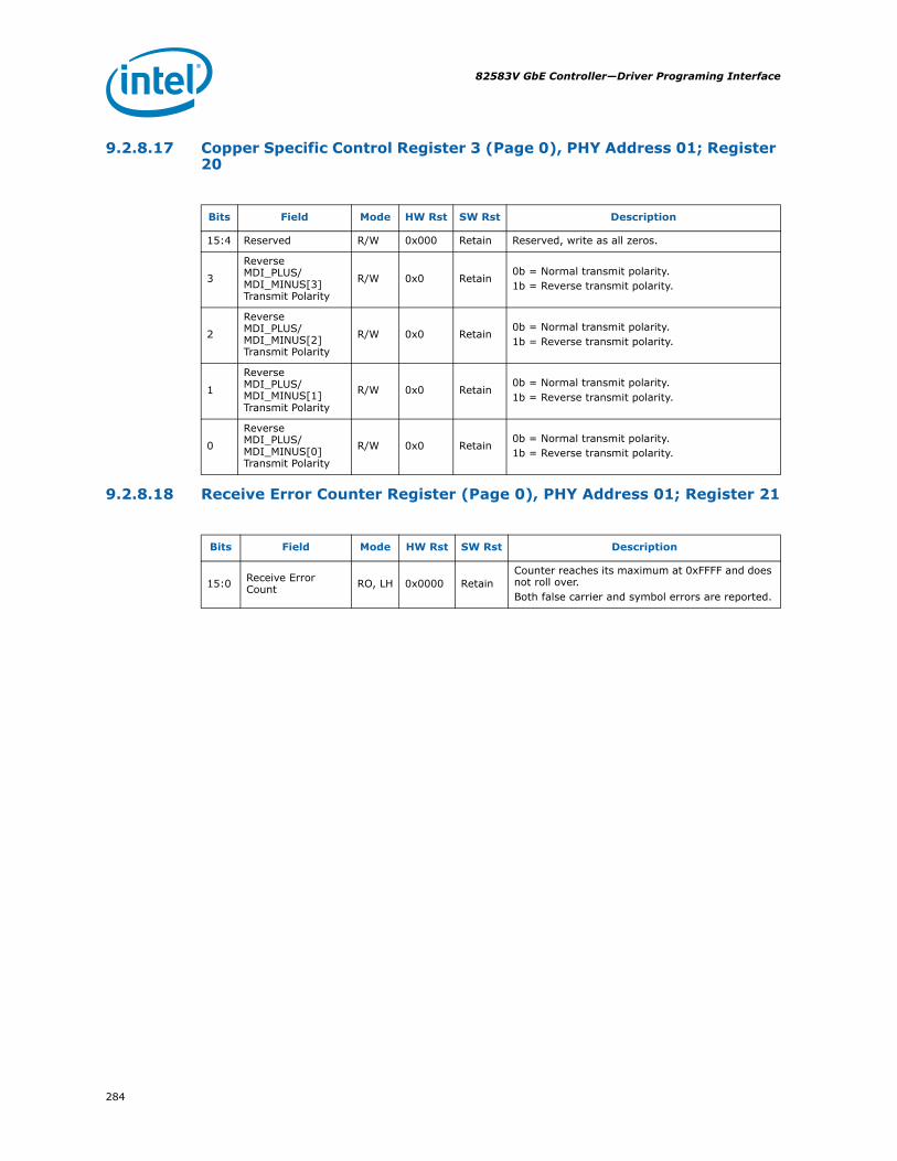
82583V GbE Controller—Driver Programing Interface
284
9.2.8.17 Copper Specific Control Register 3 (Page 0), PHY Address 01; Register 20
9.2.8.18 Receive Error Counter Register (Page 0), PHY Address 01; Register 21
Bits Field Mode HW Rst SW Rst Description
15:4 Reserved R/W 0x000 Retain Reserved, write as all zeros.
3
Reverse MDI_PLUS/ MDI_MINUS[3] Transmit Polarity
R/W 0x0 Retain0b = Normal transmit polarity.1b = Reverse transmit polarity.
2
Reverse MDI_PLUS/ MDI_MINUS[2] Transmit Polarity
R/W 0x0 Retain0b = Normal transmit polarity.1b = Reverse transmit polarity.
1
Reverse MDI_PLUS/ MDI_MINUS[1] Transmit Polarity
R/W 0x0 Retain0b = Normal transmit polarity.1b = Reverse transmit polarity.
0
Reverse MDI_PLUS/ MDI_MINUS[0] Transmit Polarity
R/W 0x0 Retain0b = Normal transmit polarity.1b = Reverse transmit polarity.
Bits Field Mode HW Rst SW Rst Description
15:0 Receive Error Count RO, LH 0x0000 Retain
Counter reaches its maximum at 0xFFFF and does not roll over. Both false carrier and symbol errors are reported.

285
Driver Programing Interface—82583V GbE Controller
9.2.8.19 Page Address (Any Page), PHY Address 01; Register 22
9.2.8.20 OEM Bits (Page 0), PHY Address 01; Register 25
Bits Field Mode HW Rst SW Rst Description
15:8 Reserved RO Always 0x00
Always 0x00 Reserved, always set to 0x00.
7:0 Page Select for Registers 0 to 28 R/W 0x00 Retain Page number.
Bits Field Mode HW Rst SW Rst Description
15:11 Reserved R/W 0x0 0x0 Reserved, set to 0x0.
10 Aneg_now R/W 0b 0b Restart auto-negotiation. Note that this bit is self clearing.
9:7 Reserved R/W 0x0 0x0 Reserved, set to 0x0.
6 a1000_dis R/W 0b Retain GbE disable.
5:3 Reserved R/W 0x0 0x0 Reserved, set to 0x0.
2 rev_aneg R/W 0b Retain LPLU.
1:0 Reserved R/W 0x0 0x0 Reserved, set to 0x0.

82583V GbE Controller—Driver Programing Interface
286
9.2.8.21 Copper Specific Control Register 2 (Page 0), PHY Address 01; Register 26
Bits Field Mode HW Rst SW Rst Description
15 1000 BASE-T Transmitter Type R/W 0x0 Retain
0b = Class B.1b = Class A.
14 Disable 1000BASE-T R/W See
Description Retain
When set to disabled, 1000BASE-T is not advertised even if registers 9.9 or 9.8 are set to 1b. A write to this register bit does not take effect until any one of the following occurs:• Software reset is asserted (register 0.15).• Restart auto-negotiation is asserted
(register 0.9).• Power down (register 0.11, 16_0.2)
transitions from power down to normal operation.
• Copper link goes down. After a hardware reset, this bit defaults as follows: • ps_a1000_dis_s - bit 26_0.14 - 0, 0, 1, 1.• When ps_a1000_dis_s transitions from
one to zero, this bit is set to 0b. • When ps_a1000_dis_s transitions from
zero to one, this bit is set to 1b.1b = Disable 1000BASE-T advertisement.0b = Enable 1000BASE-T advertisement.
13 Reverse Autoneg R/W See Description Retain
A write to this register bit does not take effect until any one of the following occurs:• Software reset is asserted (register 0.15).• Restart auto-negotiation is asserted
(register 0.9).• Power down (register 0.11, 16_0.2)
transitions from power down to normal operation.
• Copper link goes down. After a hardware reset, this bit defaults as follows: • pd_rev_aneg_a - bit 26_0.13 - 0, 0, 1, 1.• When pd_rev_aneg_a transitions from
one to zero this bit will be set to 0b.• When pd_rev_aneg_a transitions from
zero to one this bit will be set to 1b.1b = Reverse auto-negotiation.0b = Normal auto-negotiation.
12 100 BASE-T Transmitter Type R/W 0x0 Retain
0b = Class B.1b = Class A.
11:4 Reserved R/W 0x00 Retain Reserved, write as 0x00.
3:2 100 MB Test Select R/W 0x0 Retain
0xb = Normal operation.10b = Select 112 ns sequence.11b = Select 16 ns sequence.
1 10 BT Polarity Force R/W 0x0 Retain
1b = Force negative polarity for receive only.0b = Normal operation.
0 Reserved R/W 0x0 Retain Reserved, write as 0x0.

287
Driver Programing Interface—82583V GbE Controller
9.2.8.22 Bias Setting Register 1 (Page 0), PHY Address 01; Register 29
9.2.8.23 Bias Setting Register 2 (Page 0), PHY Address 01; Register 30
9.2.8.24 MAC Specific Control Register 1 (Page 2), PHY Address 01; Register 16
Bits Field Mode HW Rst SW Rst Description
15:0 Bias setting1 R/W Retain
Used to optimize PHY performance in 1000Base-T mode. Set to 0x0003 when initializing the 82583V to improve BER performance.
Bits Field Mode HW Rst SW Rst Description
15:0 Bias setting2 R/W Retain
Used to optimize PHY performance in 1000Base-T mode. Set to 0x0000 when initializing the 82583V to improve BER performance.
Bits Field Mode HW Rst SW Rst Description
15:14 Transmit FIFO Depth R/W 0x0 Retain
1000BASE-T:00b = ± 16 bits.01b = ± 24 bits.10b = ± 32 bits.11b = ± 40 bits.
13:10 Reserved R/W 0x00 Retain Reserved, set to 0x00.
9 Disable fi_125_clk R/W See
Description Retain
Changes to this bit are disruptive to the normal operation; therefore, any changes to these registers must be followed by a software reset to take effect.After a hardware reset, this bit takes on the value of pd_pwrdn_clk125_a. When pd_pwrdn_clk125_a transitions from one to zero this bit is set to 0b. When pd_pwrdn_clk125_a transitions from zero to one this bit is set to 1b.1b = fi_125_clk low.0b = fi_125_clk toggle
8 Disable fi_50_clk R/W See
Description Retain
After a hardware reset, this bit takes on the value of pd_pwrdn_clk50_a. When pd_pwrdn_clk50_a transitions from one to zero this bit is set to 0b. When pd_pwrdn_clk50_a transitions from zero to one this bit is set to 1b.1b = fi_50_clk low.0b = fi_50_clk toggle.
7 Reserved R/W 0x1 Update Reserved, write as 0x1.
6:4 Reserved R/W 0x0 Retain Reserved, write as 0x00.
3
GMII Interface Power Down
R/W 0x1 Update
Changes to this bit are disruptive to the normal operation; therefore, any changes to these registers must be followed by a software reset to take effect.This bit determines whether the GMII RX_CLK powers down when register 0.11, 16_0.2 are used to power down the 82583V or when the PHY enters the energy detect state.1b = Always power up.0b = Can power down.
2:0 Reserved R/W 0x0 Retain Reserved, write as 0x00.
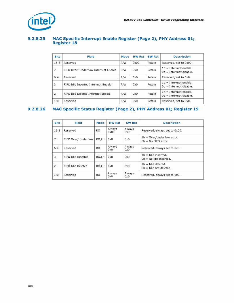
82583V GbE Controller—Driver Programing Interface
288
9.2.8.25 MAC Specific Interrupt Enable Register (Page 2), PHY Address 01; Register 18
9.2.8.26 MAC Specific Status Register (Page 2), PHY Address 01; Register 19
Bits Field Mode HW Rst SW Rst Description
15:8 Reserved R/W 0x00 Retain Reserved, set to 0x00.
7 FIFO Over/ Underflow Interrupt Enable R/W 0x0 Retain1b = Interrupt enable.0b = Interrupt disable.
6:4 Reserved R/W 0x0 Retain Reserved, set to 0x0.
3 FIFO Idle Inserted Interrupt Enable R/W 0x0 Retain1b = Interrupt enable.0b = Interrupt disable.
2 FIFO Idle Deleted Interrupt Enable R/W 0x0 Retain1b = Interrupt enable.0b = Interrupt disable.
1:0 Reserved R/W 0x0 Retain Reserved, set to 0x0.
Bits Field Mode HW Rst SW Rst Description
15:8 Reserved RO Always 0x00
Always 0x00 Reserved, always set to 0x00.
7 FIFO Over/ Underflow RO,LH 0x0 0x01b = Over/underflow error.0b = No FIFO error.
6:4 Reserved RO Always 0x0
Always 0x0 Reserved, always set to 0x0.
3 FIFO Idle Inserted RO,LH 0x0 0x01b = Idle inserted.0b = No idle inserted.
2 FIFO Idle Deleted RO,LH 0x0 0x01b = Idle deleted.0b = Idle not deleted.
1:0 Reserved RO Always 0x0
Always 0x0 Reserved, always set to 0x0.

289
Driver Programing Interface—82583V GbE Controller
9.2.8.27 MAC Specific Control Register 2 (Page 2), PHY Address 01; Register 21
9.2.8.28 LED[3:0] Function Control Register (Page 3), PHY Address 01; Register 16
Bits Field Mode HW Rst SW Rst Description
15:14 Reserved R/W 0x0 0x0 Reserved, set to 0x0.
13:12 Reserved R/W 0x1 Update Reserved, set to 0x1.
11:7 Reserved R/W 0x00 0x00 Reserved, set to 0x00.
6 Reserved R/W 0x1 Update Reserved, set to 0x1.
5:4 Reserved R/W 0x0 Retain Reserved, set to 0x0.
3 Block Carrier Extension Bit R/W 0x0 Retain
1b = Enable block carrier extension.0b = Disable block carrier extension.
2:0Default MAC Interface Speed
R/W 0x6 Update
Changes to these bits are disruptive to the normal operation; therefore, any changes to these registers must be followed by software reset to take effect.MAC interface speed during link down while auto- negotiation is enabled and TX_CLK speed bit speed link down 1000BASE-T.000b = 10 Mb/s 2.5 MHz 0 MHz.001b = 100 Mb/s 25 MHz 0 MHz.01xb = 1000 Mb/s 0 MHz 0 MHz.100b = 10 Mb/s 2.5 MHz 2.5 MHz.101b = 100 Mb/s 25 MHz 25 MHz.110b = 1000 Mb/s 2.5 MHz 2.5 MHz.111b = 1000 Mb/s 25 MHz 25 MHz.
Bits Field Mode HW Rst SW Rst Description
15:12 LED[3] Control R/W See
Description Retain
If 16_3.11:10 is set to 11b, then 16_3.15:12 has no effect.0000b = Reserved.0001b = On - link, blink - activity, off - no link.0010b = On - link, blink - receive, off - no link.0011b = On - activity, off - no activity0100b = Blink - activity, off - no activity.0101b = On - transmit, off - no transmit.0110b = On - 10 Mb/s or 1000 Mb/s master, off.
Else
0111b = On - full duplex, off - half-duplex.1000b = Force off.1001b = Force on.1010b = Force hi-Z.1011b = Force blink.11xxb = Reserved.After a hardware reset, this bit is a function of pd_config_led_a[1:0].00b = 0001b.01b = 0001b.10b = 0111b.11b = 0001b.

82583V GbE Controller—Driver Programing Interface
290
Bits Field Mode HW Rst SW Rst Description
11:8 LED[2] Control R/W See
Description Retain
0000b = On - link, off - no link.0001b = On - link, blink - activity, off - no link.0010b = Reserved.0011b = On - activity, off - no activity.0100b = Blink - activity, off - no activity.0101b = On - transmit, off - no transmit.0110b = On - 10/1000 Mb/s link, off.
Else
0111b = On - 10 Mb/s link, off.
Else
1000b = Force off.1001b = Force on.1010b = Force hi-Z.1011b = Force blink.1100b = Mode 1 (dual LED mode).1101b = Mode 2 (dual LED mode).1110b = Mode 3 (dual LED mode).1111b = Mode 4 (dual LED mode).After a hardware reset, this bit is a function of pd_config_led_a[1:0].00b = 0000b.01b = 0111b.10b = 0001b.11b = 0111b.
7:4 LED[1] Control R/W See
Description Retain
If 16_3.3:2 is set to 11b, then 16_3.7:4 has no effect.0000b = Reserved.0001b = On - link, blink - activity, off - no link.0010b = On - link, blink - receive, off - no link.0011b = On - activity, off - no activity.0100b = Blink - activity, off - no activity.0101b = Reserved.0110b = On - 100/1000 Mb/s link, off.
Else
0111b = On - 100 Mb/s link, off.
Else
1000b = Force off.1001b = Force on.1010b = Force hi-Z.1011b = Force blink.11xxb = Reserved.After a hardware reset, this bit is a function of pd_config_led_a[1:0].00b = 0001b.01b = 0111b.10b = 0111b.11b = 0111b.

291
Driver Programing Interface—82583V GbE Controller
Bits Field Mode HW Rst SW Rst Description
3:0 LED[0] Control R/W See
Description Retain
0000b = On - link, off - no link.0001b = On - link, blink - activity, off - no link.0010b = 3 blinks - 1000 Mb/s 2 blinks - 100 Mb/s 1 blink - 10 Mb/s 0 blink - no link.0011b = On - activity, off - no activity.0100b = Blink - activity, off - no activity.0101b = On - transmit, off - no transmit.0110b = On - copper link, off.
Else
0111b = On - 1000 Mb/s link, off.
Else
1000b = Force off.1001b = Force on.1010b = Force hi-Z.1011b = Force blink.1100b = Mode 1 (dual LED mode).1101b = Mode 2 (dual LED mode).1110b = Mode 3 (dual LED mode).1111b = Mode 4 (dual LED mode).After a hardware reset this bit is a function of pd_config_led_a[1:0].00b = 1110b.01b = 0111b.10b = 0111b.11b = 0111b.
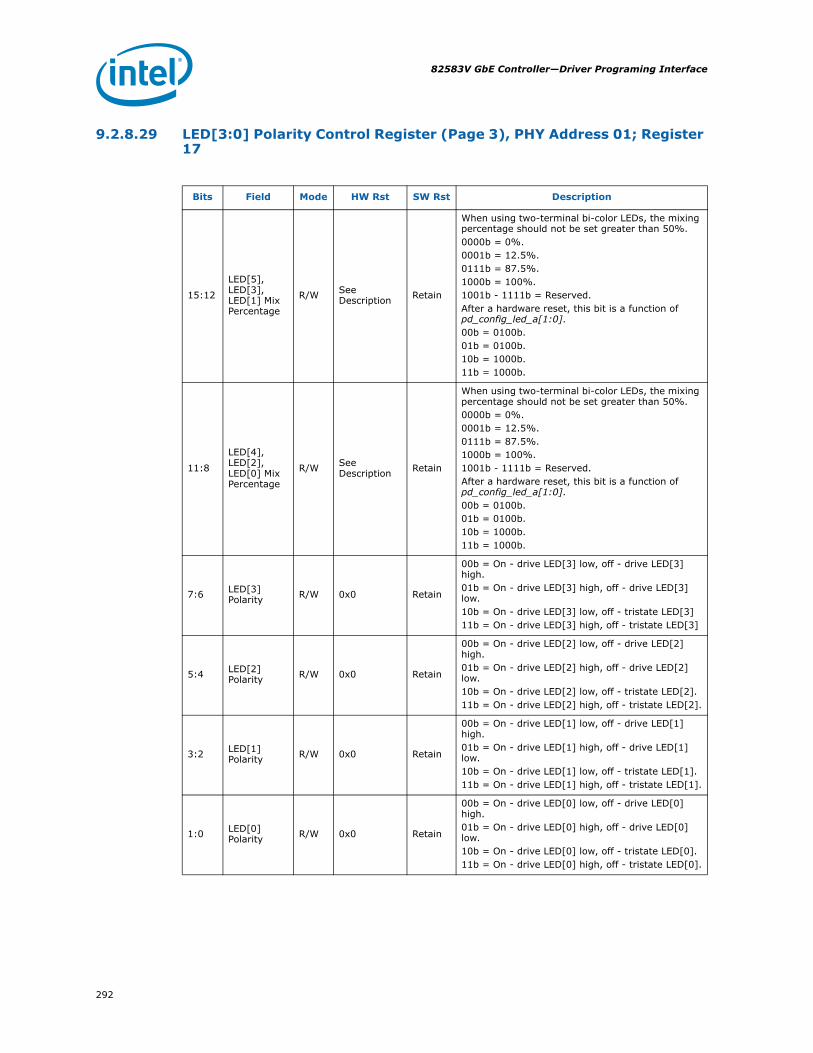
82583V GbE Controller—Driver Programing Interface
292
9.2.8.29 LED[3:0] Polarity Control Register (Page 3), PHY Address 01; Register 17
Bits Field Mode HW Rst SW Rst Description
15:12
LED[5], LED[3], LED[1] Mix Percentage
R/W See Description Retain
When using two-terminal bi-color LEDs, the mixing percentage should not be set greater than 50%.0000b = 0%.0001b = 12.5%.0111b = 87.5%.1000b = 100%.1001b - 1111b = Reserved.After a hardware reset, this bit is a function of pd_config_led_a[1:0].00b = 0100b.01b = 0100b.10b = 1000b.11b = 1000b.
11:8
LED[4], LED[2], LED[0] Mix Percentage
R/W See Description Retain
When using two-terminal bi-color LEDs, the mixing percentage should not be set greater than 50%.0000b = 0%.0001b = 12.5%.0111b = 87.5%.1000b = 100%.1001b - 1111b = Reserved.After a hardware reset, this bit is a function of pd_config_led_a[1:0].00b = 0100b.01b = 0100b.10b = 1000b.11b = 1000b.
7:6 LED[3] Polarity R/W 0x0 Retain
00b = On - drive LED[3] low, off - drive LED[3] high.01b = On - drive LED[3] high, off - drive LED[3] low.10b = On - drive LED[3] low, off - tristate LED[3]11b = On - drive LED[3] high, off - tristate LED[3]
5:4 LED[2] Polarity R/W 0x0 Retain
00b = On - drive LED[2] low, off - drive LED[2] high.01b = On - drive LED[2] high, off - drive LED[2] low.10b = On - drive LED[2] low, off - tristate LED[2].11b = On - drive LED[2] high, off - tristate LED[2].
3:2 LED[1] Polarity R/W 0x0 Retain
00b = On - drive LED[1] low, off - drive LED[1] high.01b = On - drive LED[1] high, off - drive LED[1] low.10b = On - drive LED[1] low, off - tristate LED[1].11b = On - drive LED[1] high, off - tristate LED[1].
1:0 LED[0] Polarity R/W 0x0 Retain
00b = On - drive LED[0] low, off - drive LED[0] high.01b = On - drive LED[0] high, off - drive LED[0] low.10b = On - drive LED[0] low, off - tristate LED[0].11b = On - drive LED[0] high, off - tristate LED[0].

293
Driver Programing Interface—82583V GbE Controller
9.2.8.30 LED Timer Control Register (Page 3), PHY Address 01; Register 18
Bits Field Mode HW Rst SW Rst Description
15 Force INT R/W 0x0 Retain1b = Interrupt pin asserted is forced.0b = Normal operation.
14:12Pulse Stretch Duration
R/W 0x4 Retain
000b = No pulse stretching.001b = 21 ms to 42 ms.010b = 42 ms to 84 ms.011b = 84 ms to 170 ms.100b = 170 ms to 340 ms.101b = 340 ms to 670 ms.110b = 670 ms to 1.3 s.111b = 1.3 s to 2.7 s
11 Interrupt Polarity R/W See
Description Retain
After a hardware reset, this bit takes on the value of pd_config_intpol_a.0b = jt_int_s active high.1b = jt_int_a active low
10:8 Blink Rate R/W See Description Retain
000b = 42 ms.001b = 84 ms.010b = 170 ms.011b = 340 ms.100b = 670 ms.101b to 111b = Reserved.After a hardware reset, this bit is a function of pd_config_led_a[1:0].00b = 001b.01b = 000b.10b = 001b.11b = 001b.
7:4 Reserved R/W 0x0 Retain Reserved, set to 0x0.
3:2 Speed Off Pulse Period R/W 0x1 Retain
00b = 84 ms.01b = 170 ms.10b = 340 ms.11b = 670 ms.
1:0 Speed On Pulse Period R/W 0x1 Retain
00b = 84 ms.01b = 170 ms.10b = 340 ms.11b = 670 ms.

82583V GbE Controller—Driver Programing Interface
294
9.2.8.31 LED[5:4] Function Control and Polarity Register (Page 3), PHY Address 01; Register 19
Bits Field Mode HW Rst SW Rst Description
15:12 Reserved R/W 0x0 Retain Reserved, set to 0x0.
11:10 LED[5] Polarity R/W 0x0 Retain
00b = On - drive LED[5] low, off - drive LED[5] high.01b = On - drive LED[5] high, off - drive LED[5] low.10b = On - drive LED[5] low, off - tristate LED[5].11b = On - drive LED[5] high, off - tristate LED[5].
9:8 LED[4] Polarity R/W 0x0 Retain
00b = On - drive LED[4] low, off - drive LED[4] high.01b = On - drive LED[4] high, off - drive LED[4] low.10b = On - drive LED[4] low, off - tristate LED[4].11b = On - drive LED[4] high, off - tristate LED[4].
7:4 LED[5] Control R/W See
Description Retain
If 19_3.3:2 is set to 11b, then 19_3.7:4 has no effect.0000b = On - receive, off - no receive.0001b = On - link, blink - activity, off - no link.0010b = On - link, blink - receive, off - no link.0011b = On - activity, off - no activity.0100b = Blink - activity, off - no activity.0101b = On - transmit, off - no transmit.0110b = On - full-duplex, off - half-duplex.0111b = On - full-duplex, blink - collision off - half duplex.1000b = Force off.1001b = Force on.1010b = Force hi-Z.1011b = Force blink.11xxb = Reserved.After a hardware reset, this bit is a function of pd_config_led_a[1:0].00b = 0111b.01b = 0100b.10b = 0111b.11b = 0111b.
3:0 LED[4] Control R/W See
Description Retain
0000b = On - receive, off - no receive.0001b = On - link, blink - activity, off - no link.0010b = On - link, blink - receive, off - no link.0011b = On - activity, off - no activity.0100b = Blink - activity, off - no activity.0101b = On - transmit, off - no transmit.0110b = On - full-duplex, off - half-duplex.0111b = On - full-duplex, blink - collision off - half duplex.1000b = Force off.1001b = Force on.1010b = Force hi-Z.1011b = Force blink.1100b = Mode 1 (dual LED mode).1101b = Mode 2 (dual LED mode).1110b = Mode 3 (dual LED mode).1111b = Mode 4 (dual LED mode).After a hardware reset, this bit is a function of pd_config_led_a[1:0].00b = 0011b.01b = 0110b.10b = 0011b.11b = 0011b.

295
Driver Programing Interface—82583V GbE Controller
9.2.8.32 1000 BASE-T Pair Skew Register (Page 5), PHY Address 01; Register 20
9.2.8.33 1000 BASE-T Pair Swap and Polarity (Page 5), PHY Address 01; Register 21
9.2.8.34 CRC Counters (Page 6), PHY Address 01; Register 17
Bits Field Mode HW Rst SW Rst Description
15:12 Pair 7,8 (MDI[3]±) RO 0x0 0x0
Skew = bit value times 8 ns. The value is correct to within ± 8 ns. The contents of 20_5.15:0 are valid only if register 21_5.6 = 1b.
11:8 Pair 4,5 (MDI[2]±) RO 0x0 0x0 Skew = bit value times 8 ns. The value is correct to
within ± 8 ns.
7:4 Pair 3,6 (MDI[1]±) RO 0x0 0x0 Skew = bit value times 8 ns. The value is correct to
within ± 8 ns.
3:0 Pair 1,2 (MDI[0]±) RO 0x0 0x0 Skew = bit value times 8 ns. The value is correct to
within ± 8 ns.
Bits Field Mode HW Rst SW Rst Description
15:7 Reserved RO 0x000 0x000
6 Register 20_5 And 21_5 Valid RO 0x0 0x0
The contents of 21_5.5:0 and 20_5.15:0 are valid only if register 21_5.6 = 1b.1b = Valid.0b = Invalid.
5 C, D Crossover RO 0x0 0x0
1b = Channel C received on MDI[2]± Channel D received on MDI[3]±.0b = Channel D received on MDI[2]± Channel C received on MDI[3]±.
4 A, B Crossover RO 0x0 0x0
1b = Channel A received on MDI[0]± Channel B received on MDI[1]±.0b = Channel B received on MDI[0]± Channel A received on MDI[1]±.
3 Pair 7,8 (MDI[3]±) Polarity RO 0x0 0x0
1b = Negative.0b = Positive.
2 Pair 4,5 (MDI[2]±) Polarity 0x0 0x0
1b = Negative.0b = Positive.
1 Pair 3,6 (MDI[1]±) Polarity RO 0x0 0x0
1b = Negative.0b = Positive.
0 Pair 1,2 (MDI[0]±) Polarity RO 0x0 0x0
1b = Negative.0b = Positive.
Bits Field Mode HW Rst SW Rst Description
15:8 CRC Packet Count RO 0x00 Retain
0x00 = No packets received.0xFF = 256 packets received (maximum count). Bit 16_6.4 must be set to 1b in order for the register to be valid.
7:0 CRC Error Count RO 0x00 Retain
0x00 = no CRC errors detected in the packets received.0xFF = 256 CRC errors detected in the packets received (maximum count). Bit 16_6.4 must be set to 1b in order for the register to be valid.

82583V GbE Controller—Driver Programing Interface
296
9.2.9 Diagnostic Register Descriptions
The 82583V contains several diagnostic registers. These registers enable software to directly access the contents of the 82583V’s internal Packet Buffer Memory (PBM), also referred to as FIFO space. These registers also give software visibility into what locations in the PBM the hardware currently considers to be the head and tail for both transmit and receive operations.
9.2.9.1 PHY OEM Bits Register - POEMB (0x00F10; RW)
The bits in this register are connected to the PHY interface. They affect the auto-negotiation speed resolution and enable GbE mode. Additionally, PHY class A or B drivers are also controlled.
Note: When software changes LPLU, D0LPLU or an1000_dis_nd0a it must wait at least 80 ns and then force the link to auto-negotiate in order to commit the changes to the PHY.
9.2.9.2 Receive Data FIFO Head Register - RDFH (0x02410; RW)
Field Bit(s) Initial Value Description
Reserved 0 1b1
1. Bits 7:0 of this register are loaded from NVM word 0x1C[15:8].
Reserved
d0lplu 1 0b1 PHY auto negotiation for slowest possible link (reverse auto-negotiation) in all power states. This bit overrides the LPLU bit.
lplu 2 1b1 Enables PHY auto-negotiation for slowest possible link (reverse auto-negotiation) in all power states except D0a (DR, D0u and D3).
an1000_dis_nd0a 3 1b1 Prevents PHY from auto negotiating 1000 Mb/s link in all power states
except D0a (DR, D0u and D3).
class_ab 4 0b1 Class AB driver.
reautoneg_now 5 0b1 This bit can be written by software to force link auto re-negotiation.
1000_dis 6 0b1 Prevents PHY auto-negotiating 1000 Mb/s link in all power states.
Auto_update 7 0b1Auto-update CBDisable auto update of the Flash from the shadow RAM when the ER_RD register is written.
Pause 8 1bControls the pause advertisements by the PHY.1b = MAC pause implemented.0b = MAC pause not implemented.
Asymmetric Pause 9 1b
Controls the metric pause advertisement by the PHY.1b = Asymmetric pause supported.0b = Semantics pause not supported.
Reserved 31:10 0x0 Reserved
Field Bit(s) Initial Value Description
FIFO Head 12:0 0x0 Receive FIFO Head Pointer
Reserved 31:13 0x0 Reads as 0x0. Should be written to 0x0 for future compatibility.

297
Driver Programing Interface—82583V GbE Controller
This register stores the head pointer of the on–chip receive data FIFO. Since the internal FIFO is organized in units of 64-bit words, this field contains the 64-bit offset of the current receive FIFO head. So a value of 0x8 in this register corresponds to an offset of eight Qwords or 64 bytes into the receive FIFO space. This register is available for diagnostic purposes only, and should not be written during normal operation.
Note: This register’s address has been moved from where it was located in previous devices. However, for backwards compatibility, this register can also be accessed at its alias offset of 0x08000. In addition, with the 82583V, the value in this register contains the offset of the receive FIFO head relative to the beginning of the entire PBM space. Alternatively, with previous devices, the value in this register contains the relative offset to the beginning of the receive FIFO space (within the PBM space).
9.2.9.3 Receive Data FIFO Tail Register - RDFT (0x02418; RW)
This register stores the tail pointer of the on–chip receive data FIFO. Since the internal FIFO is organized in units of 64 bit words, this field contains the 64 bit offset of the current Receive FIFO Tail. So a value of “0x8” in this register corresponds to an offset of 8 QWORDS or 64 bytes into the Receive FIFO space. This register is available for diagnostic purposes only, and should not be written during normal operation.
Note: This register’s address has been moved from where it was located in previous devices. However, for backwards compatibility, this register can also be accessed at its alias offset of 0x08008. In addition, with the 82583V, the value in this register contains the offset of the receive FIFO tail relative to the beginning of the entire PBM space. Alternatively, with previous devices, the value in this register contains the relative offset to the beginning of the Receive FIFO space (within the PBM space).
9.2.9.4 Receive Data FIFO Head Saved Register - RDFHS (0x02420; RW)
This register stores a copy of the Receive Data FIFO Head register if the internal register needs to be restored. This register is available for diagnostic purposes only, and should not be written during normal operation.
9.2.9.5 Receive Data FIFO Tail Saved Register - RDFTS (0x02428; RW)
Field Bit(s) Initial Value Description
FIFO Tail 12:0 0x0 Receive FIFO Tail pointer.
Reserved 31:13 0x0 Reads as 0x0. Should be written to 0x0 for future compatibility.
Field Bit(s) Initial Value Description
FIFO Head 12:0 0x0 A saved value of the receive FIFO head pointer.
Reserved 31:13 0x0 Reads as 0x0. Should be written to 0x0 for future compatibility.
Field Bit(s) Initial Value Description
FIFO Tail 12:0 0x0 A saved value of the receive FIFO tail pointer.
Reserved 31:13 0x0 Reads as 0x0. Should be written to 0x0 for future compatibility.

82583V GbE Controller—Driver Programing Interface
298
This register stores a copy of the Receive Data FIFO Tail register if the internal register needs to be restored. This register is available for diagnostic purposes only, and should not be written during normal operation.
9.2.9.6 Receive Data FIFO Packet Count - RDFPC (0x02430; RW)
This register reflects the number of receive packets that are currently in the receive FIFO. This register is available for diagnostic purposes only, and should not be written during normal operation.
9.2.9.7 Transmit Data FIFO Head Register - TDFH (0x03410; RW)
This register stores the head pointer of the on–chip transmit data FIFO. Since the internal FIFO is organized in units of 64-bit words, this field contains the 64-bit offset of the current Transmit FIFO Head. So a value of 0x8 in this register corresponds to an offset of eight Qwords or 64 bytes into the transmit FIFO space. This register is available for diagnostic purposes only, and should not be written during normal operation.
Note: This register’s address has been moved from where it was located in the previous devices. However, for backwards compatibility, this register can also be accessed at its alias offset of 0x08010. In addition, with the 82583V, the value in this register contains the offset of the transmit FIFO head relative to the beginning of the entire PBM space. Alternatively, with the previous devices, the value in this register contains the relative offset to the beginning of the transmit FIFO space (within the PBM space).
9.2.9.8 Transmit Data FIFO Tail Register - TDFT (0x03418; RW)
This register stores the head pointer of the on–chip transmit data FIFO. Since the internal FIFO is organized in units of 64 bit words, this field contains the 64 bit offset of the current Transmit FIFO Tail. So a value of “0x8” in this register corresponds to an offset of 8 QWORDS or 64 bytes into the Transmit FIFO space. This register is available for diagnostic purposes only, and should not be written during normal operation.
Field Bit(s) Initial Value Description
RX FIFO Packet Count 12:0 0x0 The number of received packets currently in the RX FIFO.
Reserved 31:13 0x0 Reads as 0x0. Should be written to 0x0 for future compatibility.
Field Bit(s) Initial Value Description
FIFO Tail 12:0 0x6001
1. The initial value equals PBA.RXA times 128.
Transmit FIFO Head Pointer
Reserved 31:13 0x0 Reads as 0x0. Should be written to 0x0 for future compatibility.
Field Bit(s) Initial Value Description
FIFO Tail 12:0 0x6001
1. The initial value equals PBA.RXA times 128.
Transmit FIFO Tail Pointer
Reserved 31:13 0x0 Reads as 0x0. Should be written to 0x0 for future compatibility.

299
Driver Programing Interface—82583V GbE Controller
This register’s address has been moved from where it was located in the previous devices. However, for backwards compatibility, this register can also be accessed at its alias offset of 0x08018. In addition, with the 82583V, the value in this register contains the offset of the transmit FIFO head relative to the beginning of the entire PBM space. Alternatively, with the previous devices, the value in this register contains the relative offset to the beginning of the transmit FIFO space (within the PBM space).
9.2.9.9 Transmit Data FIFO Head Saved Register - TDFHS (0x03420; RW)
This register stores a copy of the Transmit Data FIFO Head register if the internal register needs to be restored. This register is available for diagnostic purposes only, and should not be written during normal operation.
9.2.9.10 Transmit Data FIFO Tail Saved Register - TDFTS (0x03428; RW)
This register stores a copy of the Receive Data FIFO Tail register if the internal register needs to be restored. This register is available for diagnostic purposes only, and should not be written during normal operation.
9.2.9.11 Transmit Data FIFO Packet Count - TDFPC (0x03430; RW)
This register reflects the number of packets to be transmitted that are currently in the transmit FIFO. This register is available for diagnostic purposes only, and should not be written during normal operation.
9.2.9.12 Packet Buffer Memory - PBM (0x10000 - 0x17FFF; RW)
Field Bit(s) Initial Value Description
FIFO Head 12:0 0x6001
1. The initial value equals PBA.RXA times 128.
A saved value of the Transmit FIFO Head Pointer.
Reserved 31:13 0x0 Reads as 0x0. Should be written to 0x0 for future compatibility.
Field Bit(s) Initial Value Description
FIFO Tail 12:0 0x6001
1. The initial value equals PBA.RXA times 128.
A saved value of the Transmit FIFO Tail Pointer.
Reserved 31:13 0x0 Reads as 0x0. Should be written to 0x0 for future compatibility.
Field Bit(s) Initial Value Description
TX FIFO Packet Count 12:0 0x0 The number of packets to be transmitted that are currently in the TX
FIFO.
Reserved 31:13 0x0 Reads as 0x0. Should be written to 0x0 for future compatibility.
Field Bit(s) Initial Value Description
FIFO Data 31:0 X Packet Buffer Data

82583V GbE Controller—Driver Programing Interface
300
All PBM (FIFO) data is available to diagnostics. Locations can be accessed as 32-bit or 64-bit words. The internal PBM is 40 KB in size. As mentioned in Section 9.2.7.36, software can configure the amount of PBM space that is used as the transmit FIFO versus the receive FIFO. The default is 16 KB of transmit FIFO space and 16 KB of receive FIFO space. Regardless of the individual FIFO sizes that software configures, the RX FIFO is located first in the memory mapped PBM space. So for the default FIFO configuration, the RX FIFO occupies offsets 0x10000-0x13FFF of the memory mapped space, while the TX FIFO occupies offsets 0x14000-0x17FFF of the memory mapped space.
9.2.9.13 Packet Buffer Size -PBS (0x01008; RW)
This register sets the on-chip receive and transmit storage allocation size, The allocation value is read/write for the lower six bits. The division between transmit and receive is done according to the PBA register.
Note: Programming this register does not automatically re-load or initialize internal packet-buffer RAM pointers. The software must reset both transmit and receive operation (using the global device reset CTRL.RST bit) after changing this register in order for it to take effect. The PBS register itself is not reset by asserting the global reset, but only is reset at initial hardware power on.
Note: Programming this register should be aligned with programming the PBA register. If PBA and PBS are not coordinated, hardware operation is not determined.
Field Bit(s) Initial Value Description
PBS 15:0 0x0028
Packet Buffer SizeLower six bits declare the packet buffer size both for transmit and receive in 1 KB granularity. The upper 10 bits are read as zero. The default is 40 KB.
Rsvd 31:16 0x0000 Reserved read as zero.

301
Driver Programing Interface—82583V GbE Controller
Note: This page intentionally left blank.

82583V GbE Controller—Programing Interface
302
10.0 Programing Interface
10.1 PCIe Configuration Space
10.1.1 PCIe Compatibility
PCIe is completely compatible with existing deployed PCI software. To achieve this, PCIe hardware implementations conform to the following requirements:
• All devices required to be supported by the deployed PCI software must be enumerable as part of a tree through PCI device enumeration mechanisms.
• Devices must not require any resources (such as address decode ranges and interrupts) beyond those claimed by PCI resources for operation of software compatible and software transparent features with respect to existing deployed PCI software.
• Devices in their default operating state must conform to PCI ordering and cache coherency rules from a software viewpoint.
• PCIe devices must conform to PCI power management specification. PCIe devices must not require any register programming for PCI-compatible power management, beyond those available through PCI power management capability registers. Power management is expected to conform to standard PCI power management using existing PCI bus drivers.
PCIe devices implement all registers required by the PCI specification as well as the power management registers and capability pointers specified by the PCI power management specification. In addition, PCIe defines a PCIe capability pointer to indicate support for PCIe extensions and associated capabilities.
Note: The 82583V is a single function device - the LAN function.
The 82583V contains the following regions of the PCI configuration space:• Mandatory PCI configuration registers• Power management capabilities• MSI capabilities• PCIe extended capabilities

303
Programing Interface—82583V GbE Controller
10.1.2 Mandatory PCI Configuration Registers
The PCI configuration registers map is depicted below. See a detailed description for registers loaded from the NVM at initialization time. Initialization values of the configuration registers are marked in parenthesis. Color Notation in Figure 44:
Light Blue Read-only fields
Dark Grey Not used. Hardwired to zero.
Configuration registers are assigned one of the attributes described in Table 52.
Table 52. R/W Attribute Table
R/W Attribute Description
RO Read-only register: Register bits are read-only and cannot be altered by software.
RW Read-write register: Register bits are read-write and can be either set or reset.
R/W1C Read-only status, Write-1-to-clear status register, Writing a 0b to R/W1C bits has no effect.
ROS
Read-only register with sticky bits: Register bits are read-only and cannot be altered by software. Bits are not cleared by reset and can only be reset with the PWRGOOD signal. Devices that consume AUX power are not allowed to reset sticky bits when AUX power consumption (either via AUX power or PME Enable) is enabled.
RWS
Read-write register with sticky bits: Register bits are read-write and can be either set or reset by software to the desired state. Bits are not cleared by reset and can only be reset with the PWRGOOD signal. Devices that consume AUX power are not allowed to reset sticky bits when AUX power consumption (either via AUX power or PME Enable) is enabled.
R/W1CS
Read-only status, Write-1-to-clear status register with sticky bits: Register bits indicate status when read, a set bit indicating a status event can be cleared by writing a 1b. Writing a 0b to R/W1C bits has no effect. Bits are not cleared by reset and can only be reset with the PWRGOOD signal. Devices that consume AUX power are not allowed to reset sticky bits when AUX power consumption (either via AUX power or PME Enable) is enabled.
HwInitHardware Initialized: Register bits are initialized by firmware or hardware mechanisms such as pin strapping or serial NVM. Bits are read-only after initialization and can only be reset (for write-once by firmware) with PWRGOOD signal.
RsvdP Reserved and Preserved: Reserved for future R/W implementations; software must preserve value read for writes to bits.
RsvdZ Reserved and Zero: Reserved for future R/W1C implementations; software must use 0b for writes to bits.
Byte Offset Byte 3 Byte 2 Byte 1 Byte 0
0x0 Device ID Vendor ID (0x8086)
0x4 Status Register (0x0010) Command Register (0x0000)
0x8 Class Code (0x020000) Revision ID (0x00)
0xC BIST (0x00) Header Type (0x00 | 0x80) Latency Timer (0x00) Cache Line Size
(0x10)
0x10 Base Address 0
0x14 Base Address 1
0x18 Base Address 2
0x1C Base Address 3
0x20 Base Address 4
0x24 Base Address 5

82583V GbE Controller—Programing Interface
304
Figure 44. PCI-Compatible Configuration Registers
Explanation of the various registers in the 82583V is as follows.
10.1.2.1 Vendor ID (Offset 0x0)
This is a read-only register that has the same value for all PCI functions. It uniquely identifies Intel products. The field default value is 0x8086.
10.1.2.2 Device ID (Offset 0x2)
This is a read-only register. The value is loaded from NVM. Default value is 0x150C for the 82583V.
10.1.2.3 Command Reg (Offset 0x4)
Read-write register. Layout is as follows. Shaded bits are not used by this implementation and are hardwired to 0b.
0x28 Cardbus CIS Pointer (0x00000000)
0x2C Subsystem ID (0x0000) Subsystem Vendor ID (0x8086)
0x30 Expansion ROM Base Address
0x34 Reserved (0x000000) Cap_Ptr (0xC8)
0x38 Reserved (0x00000000)
0x3C Max_Latency (0x00) Min_Grant (0x00)
Interrupt Pin(0x01)
Interrupt Line(0x00)
Byte Offset Byte 3 Byte 2 Byte 1 Byte 0
PCI Function
Default Value NVM Address Meaning
LAN 0x150C 0x0D 10/100/1000 Mb/s Ethernet controller, x1 PCIe, copper
Bit(s) Init Value Description
0 0b I/O Access Enable.
1 0b Memory Access Enable.
2 0b Enable Mastering LAN R/W field.
3 0b Special Cycle Monitoring – Hardwired to 0b.
4 0b MWI Enable – Hardwired to 0b.
5 0b Palette Snoop Enable – Hardwired to 0b.
6 0b Parity Error Response.
7 0b Wait Cycle Enable – Hardwired to 0b.
8 0b SERR# Enable.
9 0b Fast Back-to-Back Enable – Hardwired to 0b.
10 0b
Interrupt DisableControls the ability of a PCIe device to generate a legacy interrupt message. When set, the device can’t generate legacy interrupt messages.
15:11 0b Reserved

305
Programing Interface—82583V GbE Controller
10.1.2.4 Status Register (Offset 0x6)
Shaded fields are not used by this implementation and are hardwired to 0b.
10.1.2.5 Revision ID (Offset 0x8)
The default revision ID of this device is 0x0. The value of the rev ID is a logic XOR between the default value and the value in the NVM word 0x1E.
10.1.2.6 Class Code (Offset 0x9)
The class code is a read-only, hard-coded value that identifies the device functionality.
LAN - 0x020000 - Ethernet Adapter
10.1.2.7 Cache Line Size (Offset 0xC)
This field is implemented by PCIe devices as a read-write field for legacy compatibility purposes but has no impact on any PCIe device functionality. Loaded from NVM words 0x1A.
10.1.2.8 Latency Timer (Offset 0xD)
Not used. Hardwired to 0b.
10.1.2.9 Header Type (Offset 0xE)
This indicates if a device is single function or multifunction. For the 82583V this field has a value of 0x00 to indicate a single function device.
Bits Initial Value R/W Description
2:0 000b Reserved
3 0b RO Interrupt Status1
4 1b RO
New CapabilitiesIndicates that a device implements extended capabilities. The 82583V sets this bit, and implements a capabilities list, to indicate that it supports PCI power management, message signaled interrupts, and the PCIe extensions.
5 0b 66MHz Capable – Hardwired to 0b.
6 0b Reserved.
7 0b Fast Back-to-Back Capable – Hardwired to 0b.
8 0b R/W1C Data Parity Reported.
10:9 00b DEVSEL Timing – Hardwired to 0b.
11 0 R/W1C Signaled Target Abort.
12 0bb R/W1C Received Target Abort.
13 0b R/W1C Received Master Abort.
14 0b R/W1C Signaled System Error.
15 0b R/W1C Detected Parity Error.
1. The Interrupt Status field is a read-only field that indicates that an interrupt message ispending internally to the device.
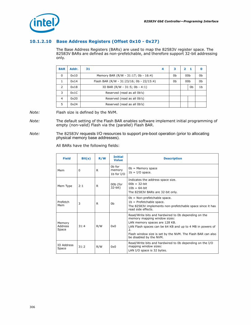
82583V GbE Controller—Programing Interface
306
10.1.2.10 Base Address Registers (Offset 0x10 - 0x27)
The Base Address Registers (BARs) are used to map the 82583V register space. The 82583V BARs are defined as non-prefetchable, and therefore support 32-bit addressing only.
Note: Flash size is defined by the NVM.
Note: The default setting of the Flash BAR enables software implement initial programming of empty (non-valid) Flash via the (parallel) Flash BAR.
Note: The 82583V requests I/O resources to support pre-boot operation (prior to allocating physical memory base addresses).
All BARs have the following fields:
BAR Addr. 31 4 3 2 1 0
0 0x10 Memory BAR (R/W - 31:17; 0b - 16:4) 0b 00b 0b
1 0x14 Flash BAR (R/W - 31:23/16; 0b - 22/15:4) 0b 00b 0b
2 0x18 IO BAR (R/W - 31:5; 0b - 4:1) 0b 1b
3 0x1C Reserved (read as all 0b’s)
4 0x20 Reserved (read as all 0b’s)
5 0x24 Reserved (read as all 0b’s)
Field Bit(s) R/W Initial Value Description
Mem 0 R0b for memory1b for I/O
0b = Memory space1b = I/O space.
Mem Type 2:1 R 00b (for 32-bit)
Indicates the address space size.00b = 32-bit10b = 64-bitThe 82583V BARs are 32-bit only.
Prefetch Mem 3 R 0b
0b = Non-prefetchable space.1b = Prefetchable space.The 82583V implements non-prefetchable space since it has read side effects.
Memory Address Space
31:4 R/W 0x0
Read/Write bits and hardwired to 0b depending on the memory mapping window sizes:LAN memory spaces are 128 KB.LAN Flash spaces can be 64 KB and up to 4 MB in powers of 2.Flash window size is set by the NVM. The Flash BAR can also be disabled by the NVM.
IO Address Space 31:2 R/W 0x0
Read/Write bits and hardwired to 0b depending on the I/O mapping window sizes:LAN I/O space is 32 bytes.

307
Programing Interface—82583V GbE Controller
Memory and I/O mapping:
10.1.2.11 CardBus CIS (Offset 0x28)
Not used. Hardwired to 0b.
10.1.2.12 Subsystem ID (Offset 0x2E)
This value can be loaded automatically from the NVM at power up with a default value of 0x0000.
10.1.2.13 Subsystem Vendor ID (Offset 0x2C)
This value can be loaded automatically from the NVM address 0x0C at power up or reset. The default value is 0x8086 at power up.
10.1.2.14 Expansion ROM Base Address (Offset 0x30)
This register is used to define the address and size information for boot-time access to the optional Flash memory. The BAR size and enablement are set by the NVM.
Mapping Window Mapping Description
MemoryBAR 0
The internal registers and memories are accessed as direct memory mapped offsets from the base address register. Software can access byte, word or Dword.
FlashBAR 1
The external Flash can be accessed using direct memory mapped offsets from the Flash base address register. Software can access byte, word or Dword.The Flash BAR is enabled by the DISLFB field in NVM word 0x21.
I/OBAR 2
All internal registers, memories, and Flash can be accessed using I/O operations. There are two 4-byte registers in the I/O mapping window: Addr Reg and Data Reg. Software can access byte, word or Dword.
Reserved Reserved
Field Bit(s) Read/Write
Initial Value Description
En 0 R/W 0b1b = Enables expansion ROM access.0b = Disables expansion ROM access.
Reserved 10:1 R 0x0 Always read as 0b. Writes are ignored.
Address 31:11 R/W 0x0Read/Write bits and hardwired to 0b depending on the memory mapping window size as defined in word 0x21 in the NVM.

82583V GbE Controller—Programing Interface
308
10.1.2.15 Cap_Ptr (Offset 0x34)
The Capabilities Pointer field (Cap_Ptr) is an 8-bit field that provides an offset in the device's PCI configuration space for the location of the first item in the capabilities linked list. The 82583V sets this bit, and implements a capabilities list, to indicate that it supports:
• PCI power management• MSI• PCIe extended capabilities
Its value, 0xC8, is the address of the first entry: PCI power management.
10.1.2.16 Interrupt Line (Offset 0x3C)
Read/write register programmed by software to indicate which of the system interrupt request lines this device's interrupt pin is bound to. See the PCI definition for more details.
10.1.2.17 Interrupt Pin (Offset 0x3D)
Read-only register. The LAN implements legacy interrupt on INTA.
10.1.2.18 Max_Lat/Min_Gnt (Offset 0x3E)
Not used. Hardwired to 0b.
10.1.3 PCI Power Management Registers
All fields are reset on full power up. All of the fields except PME_En and PME_Status are reset on exit from D3cold state.
See the detailed description for registers loaded from the NVM at initialization time. Initialization values of the configuration registers are marked in parenthesis.
Some fields in this section depend on the Power Management Ena bits in the NVM word 0x0A.
Table 53 lists the organization of the PCI Power Management register block. Light-blue fields are read only fields.
Table 53. Power Management Register Block
Address Item Next Pointer
0xC8-CF PCI power management 0xD0
0xD0-DF MSI 0xE0
0xA0-AB Reserved 0x00
0xE0-F3 PCIe Capabilities 0xA0
Byte Offset Byte 3 Byte 2 Byte 1 Byte 0
0xC8 Power Management Capabilities (PMC) Next Pointer (0xD0)
Capability ID (0x01)
0xCC Data PMCSR_BSE Bridge Support Extensions
Power Management Control / Status Register (PMCSR)

309
Programing Interface—82583V GbE Controller
The following section describes the register definitions, whether they are required or optional for compliance, and how they are implemented in the 82583V.
10.1.3.1 Capability ID, Offset 0xC8, (RO)
This field equals 0x01 indicating the linked list item is the PCI Power Management registers.
10.1.3.2 Next Pointer, Offset 0xC9, (RO)
This field provides an offset to the next capability item in the capability list. Its value of 0xD0 points to the MSI capability.
10.1.3.3 Power Management Capabilities (PMC), Offset 0xCA, (RO)
This field describes the device functionality at the power management states as described in the following table.
Figure 45. Power Management Capabilities (PMC)
Bits Default R/W Description
15:11See value in description column
RO
PME_SupportThis five-bit field indicates the power states in which the function might assert PME# depending on NVM settings:00000b = If PM is disabled in NVM (word 0x0A) than No PME support at all states. 01001b = If PM is enabled in NVM and no Aux_Pwr than PME is supported at D0 and D3hot. 11001b = If PM is Enabled in NVM and Aux_Pwr, then PME is supported at D0, D3hot and D3cold.
10 0b ROD2_SupportThe 82583V does not support D2 state
9 0b ROD1_SupportThe 82583V does not support D1 state
8:6 000b ROAUX CurrentRequired current defined in the Data register
5 1b RODSIThe 82583V requires its software device driver to be executed following transition to the D0 un-initialized state.
4 0b RO Reserved
3 0b ROPME_ClockDisabled. Hardwired to 0b.
2:0 010b ROVersionThe 82583V complies with PCI PM spec revision 1.1.

82583V GbE Controller—Programing Interface
310
10.1.3.4 Power Management Control/Status Register - (PMCSR), Offset 0xCC, (RW)
This register is used to control and monitor power management events in the 82583V.
Figure 46. Power Management Control/Status - PMCSR
10.1.3.5 PMCSR_BSE Bridge Support Extensions, Offset 0xCE, (RO)
This register is not implemented in the 82583V, values set to 0x00.
Bits Default Rd/Wr Description
15 0b at power up R/W1CPME_StatusThis bit is set to 1b when the function detects a wake-up event independent of the state of the PME_En bit. Writing a 1b clears this bit.
14:13 see value in Data register RO
Data_ScaleThis field indicates the scaling factor to be used when interpreting the value of the Data register.If the PM is enabled in the NVM, and the Data_Select field is set to 0, 3, 4 or7, than this field equals 01b (indicating 0.1 watt units). Else it equals 00b.
12:9 0000b R/W
Data_SelectThis four-bit field is used to select which data is to be reported through the Data register and Data_Scale field. These bits are writeable only when power management is enabled via the NVM.
8 0b at power up R/W
PME_EnIf power management is enabled in the NVM, writing a 1b to this register enables wake up.If power management is disabled in the NVM, writing a 1b to this bit has no affect, and does not set the bit to 1b.
7:4 000000b ROReserved The 82583V returns a value of 000000b for this field.
3 0b RO
No_Soft_ResetThis bit is always set to 0b to indicate that the 82583V performs an internal reset upon transitioning from D3hot to D0 via software control of the PowerState bits. Configuration context is lost when performing the soft reset. Upon transition from the D3hot to the D0 state, a full re-initialization sequence is needed to return the 82583V to the D0 Initialized state.
2 0b RO Reserved
1:0 00b R/W
Power State This field is used to set and report the power state of the 82583V as follows:00b = D0.01b = D1 (cycle ignored if written with this value).10b = D2 (cycle ignored if written with this value).11b = D3 (cycle ignored if PM is not enabled in the NVM).

311
Programing Interface—82583V GbE Controller
10.1.3.6 Data Register, Offset 0xCF, (RO)
This optional register is used to report power consumption and heat dissipation. Reported register is controlled by the Data_Select field in the PMCSR and the power scale is reported in the Data_Scale field in the PMCSR. The data of this field is loaded from the NVM if power management is enabled in the NVM. Otherwise, it has a default value of 0x00. The values for the 82583V are as follows:
For other Data_Select values the Data register output is reserved (0b).
10.1.4 Message Signaled Interrupt (MSI) Configuration Registers
This structure is required for PCIe devices. Initialization values of the configuration registers are marked in parenthesis. Light-blue fields represent read-only fields.
Note: There are no changes to this structure from the PCI 2.2 specification.
Figure 47. MSI Configuration Registers
10.1.4.1 Capability ID, Offset 0xD0, (RO)
This field equals 0x05 indicating the linked list item as being the MS registers.
10.1.4.2 Next Pointer, Offset 0xD1, (RO)
This field provides an offset to the next capability item in the capability list. Its value of 0xE0 points to the PCIe capability.
Function D0 (Consume/Dissipate) D3 (Consume/Dissipate)
Data Select (0x0/0x4) (0x3/0x7)
Function 0 EEPROM address 0x22 EEPROM address 0x22
Byte Offset Byte 3 Byte 2 Byte 1 Byte 0
0xD0 Message Control (0x0080) Next Pointer (0xE0) Capability ID (0x05)
0xD4 Message Address
0xD8 Message Upper Address
0xDC Reserved Message Data
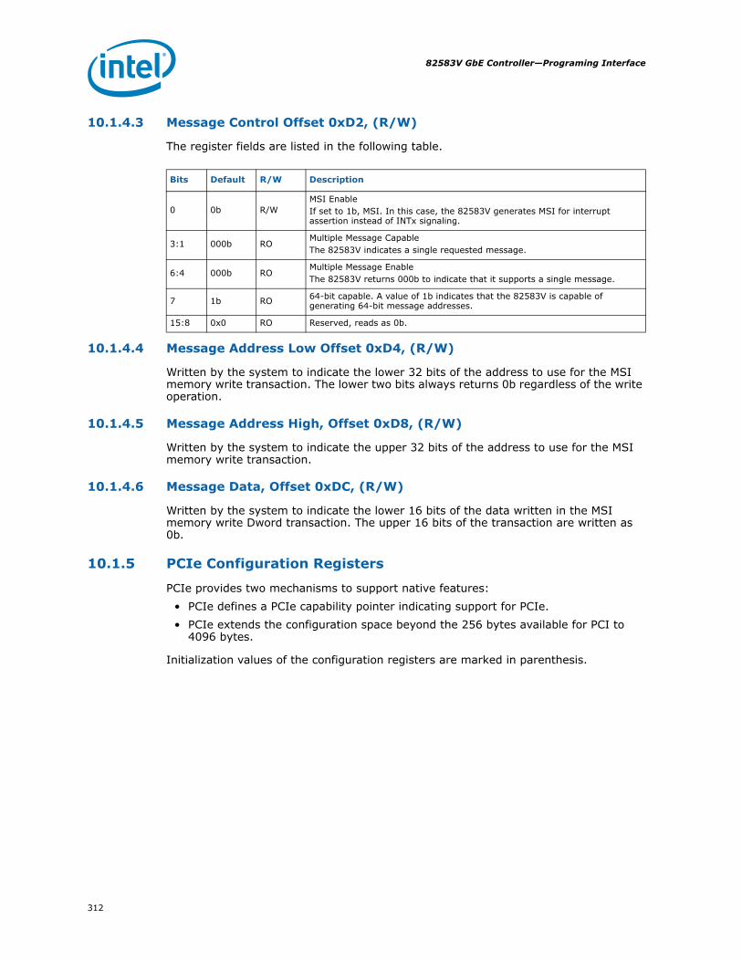
82583V GbE Controller—Programing Interface
312
10.1.4.3 Message Control Offset 0xD2, (R/W)
The register fields are listed in the following table.
10.1.4.4 Message Address Low Offset 0xD4, (R/W)
Written by the system to indicate the lower 32 bits of the address to use for the MSI memory write transaction. The lower two bits always returns 0b regardless of the write operation.
10.1.4.5 Message Address High, Offset 0xD8, (R/W)
Written by the system to indicate the upper 32 bits of the address to use for the MSI memory write transaction.
10.1.4.6 Message Data, Offset 0xDC, (R/W)
Written by the system to indicate the lower 16 bits of the data written in the MSI memory write Dword transaction. The upper 16 bits of the transaction are written as 0b.
10.1.5 PCIe Configuration Registers
PCIe provides two mechanisms to support native features:• PCIe defines a PCIe capability pointer indicating support for PCIe.• PCIe extends the configuration space beyond the 256 bytes available for PCI to
4096 bytes.
Initialization values of the configuration registers are marked in parenthesis.
Bits Default R/W Description
0 0b R/WMSI EnableIf set to 1b, MSI. In this case, the 82583V generates MSI for interrupt assertion instead of INTx signaling.
3:1 000b ROMultiple Message CapableThe 82583V indicates a single requested message.
6:4 000b ROMultiple Message EnableThe 82583V returns 000b to indicate that it supports a single message.
7 1b RO 64-bit capable. A value of 1b indicates that the 82583V is capable of generating 64-bit message addresses.
15:8 0x0 RO Reserved, reads as 0b.

313
Programing Interface—82583V GbE Controller
10.1.5.1 PCIe Capability Structure
The 82583V implements the PCIe capability structure for end-point devices as listed in Table 54.
Table 54. PCIe Configuration Registers
10.1.5.1.1 Capability ID, Offset 0xE0, (RO)
This field equals 0x10 indicating the linked list item as being the PCIe Capabilities registers.
10.1.5.1.2 Next Pointer, Offset 0xE1, (RO)
Offset to the next capability item in the capability list.
10.1.5.1.3 PCI Express CAP, Offset 0xE2, (RO)
The PCIe capabilities register identifies PCIe device type and associated capabilities. This is a read-only register.
10.1.5.1.4 Device CAP, Offset 0xE4, (RO)
This register identifies the PCIe device specific capabilities. It is a read-only register.
Byte Offset Byte 3 Byte 2 Byte 1 Byte 0
0xE0 PCIe Capability Register Next Pointer Capability ID
0xE4 Device Capability
0xE8 Device Status Device Control
0xEC Link Capability
0xF0 Link Status Link Control
Bits Default R/W Description
3:0 0001b ROCapability VersionIndicates the PCIe capability structure version number 1.
7:4 0000b RODevice/Port TypeIndicates the type of PCIe functions. LAN function in the 82583V is a native PCIe functions with a value of 0000b.
8 0b ROSlot ImplementedThe 82583V does not implement slot options therefore this field is hardwired to 0b.
13:9 00000b ROInterrupt Message NumberThe 82583V does not implement multiple MSI per function, therefore this field is hardwired to 0x0.
15:14 00b RO Reserved
Bits R/W Default Description
2:0 RO 001b
Max Payload Size SupportedThis field indicates the maximum payload that the device can support for TLPs. It is loaded from the NVM PCIe Init Configuration 3 word 0x1A (bit 8) with a default value of 256 bytes.

82583V GbE Controller—Programing Interface
314
10.1.5.1.5 Device Control, Offset 0xE8, (RW)
This register controls PCIe specific parameters.
4:3 RO 00bPhantom Function SupportedNot supported by the 82583V.
5 RO 0bExtended Tag Field SupportedMax supported size of the Tag field. The 82583V supports a 5-bit Tag field.
8:6 RO 011b
End-Point L0s Acceptable LatencyThis field indicates the acceptable latency that the 82583V can withstand due to the transition from L0s state to the L0 state. The value is loaded from the NVM PCIe Init Configuration 1 word 0x18.
11:9 RO 110b
End-Point L1 Acceptable LatencyThis field indicates the acceptable latency that the 82583V can withstand due to the transition from L1 state to the L0 state. The value is loaded from the NVM PCIe Init Configuration 1 word 0x18.
12 RO 0bAttention Button PresentHardwired in the 82583V to 0b.
13 RO 0bAttention Indicator PresentHardwired in the 82583V to 0b.
14 RO 0bPower Indicator PresentHardwired in the 82583V to 0b.
15 RO 1bRole Based Error ReportingHardwired in the 82583V to 1b.
17:16 RO 00b Reserved, set to 00b
25:18 RO 0x0Slot Power Limit ValueUsed in upstream ports only. Hardwired in the 82583V to 0x00.
27:26 RO 00bSlot Power Limit ScaleUsed in upstream ports only. Hardwired in the 82583V to 0b.
31:28 RO 0000b Reserved
Bits R/W Default Description
Bits R/W Default Description
0 RW 0bCorrectable Error Reporting EnableEnable error report.
1 RW 0bNon-Fatal Error Reporting EnableEnable error report.
2 RW 0bFatal Error Reporting Enable Enable error report.
3 RW 0bUnsupported Request Reporting EnableEnable error report.
4 RW 1b
Enable Relaxed OrderingIf this bit is set, the device is permitted to set the Relaxed Ordering bit in the attribute field of write transactions that do not need strong ordering. For more details, also see register CTRL_EXT bit RO_DIS.
7:5 RW 000b (128 Bytes)
Max Payload SizeThis field sets maximum TLP payload size for the device functions. As a receiver, the device must handle TLPs as large as the set value. As a transmitter, the device must not generate TLPs exceeding the set value.The Maximum Payload Size supported in the Device Capabilities register indicates permissible values that can be programmed.
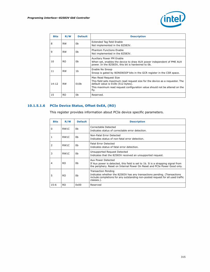
315
Programing Interface—82583V GbE Controller
10.1.5.1.6 PCIe Device Status, Offset 0xEA, (RO)
This register provides information about PCIe device specific parameters..
8 RW 0bExtended Tag field EnableNot implemented in the 82583V.
9 RW 0bPhantom Functions EnableNot implemented in the 82583V.
10 RO 0bAuxiliary Power PM EnableWhen set, enables the device to draw AUX power independent of PME AUX power. In the 82583V, this bit is hardwired to 0b.
11 RW 1bEnable No SnoopSnoop is gated by NONSNOOP bits in the GCR register in the CSR space.
14:12 RW 010b
Max Read Request SizeThis field sets maximum read request size for the device as a requester. The default value is 010b (512 bytes). This maximum read request configuration value should not be altered on the fly.
15 RO 0b Reserved.
Bits R/W Default Description
Bits R/W Default Description
0 RW1C 0bCorrectable DetectedIndicates status of correctable error detection.
1 RW1C 0bNon-Fatal Error DetectedIndicates status of non-fatal error detection.
2 RW1C 0bFatal Error DetectedIndicates status of fatal error detection.
3 RW1C 0bUnsupported Request DetectedIndicates that the 82583V received an unsupported request.
4 RO 0bAux Power DetectedIf Aux power is detected, this field is set to 1b. It is a strapping signal from the periphery. Reset on Internal Power On Reset and PCIe Power Good only.
5 RO 0b
Transaction PendingIndicates whether the 82583V has any transactions pending. (Transactions include completions for any outstanding non-posted request for all used traffic classes.).
15:6 RO 0x00 Reserved

82583V GbE Controller—Programing Interface
316
10.1.5.1.7 Link CAP, Offset 0xEC, (RO)
This register identifies PCIe link-specific capabilities. This is a read-only register.
Bits R/W Default Description
3:0 RO 0001bMax Link SpeedThe 82583V indicates a maximum link speed of 2.5 Gb/s.
9:4 RO 0x01
Max Link WidthIndicates the maximum link width. The 82583V supports x1 lane link.Defined encoding:000001b x1.All other values - Reserved.
11:10 RO 11b
Active State Link PM SupportIndicates the level of active state power management supported in the 82583V. Defined encodings are:00b = No ASPM support.01b = L0s supported.10b = L1 supported.11b = L0s and L1 supported.This field is loaded from the NVM PCIe Init Configuration 3 word 0x1A.
14:12 RO001b(64-128 ns)
L0s Exit LatencyIndicates the exit latency from L0s to L0 state. This field is loaded from the NVM PCIe Init Configuration 1 word 0x18 (two values for common PCIe clock or separate PCIe clock.000b = Less than 64 ns.001b = 64 ns – 128 ns.010b = 128 ns – 256 ns.011b = 256 ns - 512 ns.100b = 512 ns - 1 μs.101b = 1 μs – 2 μs.110b = 2 μs – 4 μs.111b = Reserved.If the 82583V uses a common clock - PCIe Init Config 1 bits [2:0], if the 82583V uses a separate clock - PCIe Init Config 1 bits [5:3].
17:15 RO110b(32-64 μs)
L1 Exit LatencyIndicates the exit latency from L1 to L0 state. This field is loaded from the NVM PCIe Init Configuration 1 word 0x18.000b = Less than 1 μs.001b = 1 μs - 2 μs.010b = 2 μs - 4 μs.011b = 4 μs - 8 μs.100b = 8 μs - 16 μs.101b = 16 μs - 32 μs.110b = 32 μs - 64 μs.111b = L1 transition not supported.
18 RO 0b Reserved.
19 RO 0b Surprise Down Error Reporting Capable.
20 RO 0b Data Link Layer Link Active Reporting Capable.
23:21 RO 000b Reserved.
31:24 HwInit 0x0Port NumberThe PCIe port number for the given PCIe link. Field is set in the link training phase.
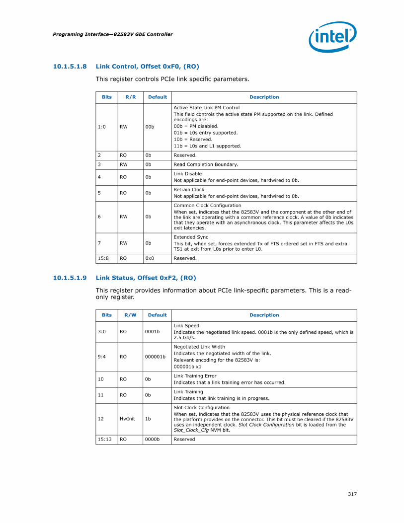
317
Programing Interface—82583V GbE Controller
10.1.5.1.8 Link Control, Offset 0xF0, (RO)
This register controls PCIe link specific parameters.
10.1.5.1.9 Link Status, Offset 0xF2, (RO)
This register provides information about PCIe link-specific parameters. This is a read-only register.
Bits R/R Default Description
1:0 RW 00b
Active State Link PM ControlThis field controls the active state PM supported on the link. Defined encodings are:00b = PM disabled.01b = L0s entry supported.10b = Reserved.11b = L0s and L1 supported.
2 RO 0b Reserved.
3 RW 0b Read Completion Boundary.
4 RO 0b Link DisableNot applicable for end-point devices, hardwired to 0b.
5 RO 0bRetrain ClockNot applicable for end-point devices, hardwired to 0b.
6 RW 0b
Common Clock ConfigurationWhen set, indicates that the 82583V and the component at the other end of the link are operating with a common reference clock. A value of 0b indicates that they operate with an asynchronous clock. This parameter affects the L0s exit latencies.
7 RW 0bExtended SyncThis bit, when set, forces extended Tx of FTS ordered set in FTS and extra TS1 at exit from L0s prior to enter L0.
15:8 RO 0x0 Reserved.
Bits R/W Default Description
3:0 RO 0001bLink SpeedIndicates the negotiated link speed. 0001b is the only defined speed, which is 2.5 Gb/s.
9:4 RO 000001b
Negotiated Link WidthIndicates the negotiated width of the link.Relevant encoding for the 82583V is:000001b x1
10 RO 0bLink Training ErrorIndicates that a link training error has occurred.
11 RO 0bLink TrainingIndicates that link training is in progress.
12 HwInit 1b
Slot Clock ConfigurationWhen set, indicates that the 82583V uses the physical reference clock that the platform provides on the connector. This bit must be cleared if the 82583V uses an independent clock. Slot Clock Configuration bit is loaded from the Slot_Clock_Cfg NVM bit.
15:13 RO 0000b Reserved

82583V GbE Controller—Programing Interface
318
10.1.5.2 PCIe Extended Configuration Space
PCIe configuration space is located in a flat memory-mapped address space. PCIe extends the configuration space beyond the 256 bytes available for PCI to 4096 bytes. The 82583V decodes additional 4-bits (bits 27:24) to provide the additional configuration space as shown. PCIe reserves the remaining 4 bits (bits 31:28) for future expansion of the configuration space beyond 4096 bytes.
The configuration address for a PCIe device is computed using PCI-compatible bus, device and function numbers as follows:
PCIe extended configuration space is allocated using a linked list of optional or required PCIe extended capabilities following a format resembling PCI capability structures. The first PCIe extended capability is located at offset 0x100 in the device configuration space. The first Dword of the capability structure identifies the capability/version and points to the next capability.
The 82583V supports the following PCIe extended capabilities:• Advanced error reporting capability - offset 0x100• Device serial number capability - offset 0x140
10.1.5.2.1 Advanced Error Reporting Capability
The PCIe advanced error reporting capability is an optional extended capability to support advanced error reporting. The following table lists the PCIe advanced error reporting extended capability structure for PCIe devices.
31 28 27 20 19 15 14 12 11 2 1 0
0000b Bus # Device # Fun # Register Address (offset) 00b
Register Offset Field Description
0x00 PCIe CAP ID PCIe Extended Capability ID.
0x04 Uncorrectable Error Status
Reports error status of individual uncorrectable error sources on a PCIe device.
0x08 Uncorrectable Error Mask
Controls reporting of individual uncorrectable errors by device to the host bridge via a PCIe error message.
0x0C Uncorrectable Error Severity
Controls whether an individual uncorrectable error is reported as a fatal error.
0x10 Correctable Error Status
Reports error status of individual correctable error sources on a PCIe device.
0x14 Correctable Error Mask
Controls reporting of individual correctable errors by device to the host bridge via a PCIe error message.
0x18 First Error Pointer Identifies the bit position of the first uncorrectable error reported in the Uncorrectable Error Status register.
0x1C:0x28 Header Log Captures the header for the transaction that generated an error.

319
Programing Interface—82583V GbE Controller
10.1.5.2.1.1 PCI Express CAP ID, Offset 0x00
10.1.5.2.1.2 Uncorrectable Error Status, Offset 0x04
The Uncorrectable Error Status register reports error status of individual uncorrectable error sources on a PCIe device. A value of 1b at a specific bit location indicates the source of the error according to the following table. Software might clear an error status by writing a 1b to the respective bit.
.
Bit Location Attribute Default Value Description
15;0 RO 0x0001Extended Capability IDPCIe extended capability ID indicating advanced error reporting capability.
19:16 RO 0x1Version NumberPCIe advanced error reporting extended capability version number.
31:20 RO 0x000/0x140
Next Capability Pointer - Next PCIe extended capability pointer. If serial number capability is enabled in NVM (PCIe init configuration 2 word), the default value is 0x140. Otherwise, it’s 0x000 indicating the end of capabilities list.
Bit Location Attribute Default Value Description
3:0 RO 0b Reserved.
4 R/W1CS 0b Data Link Protocol Error Status.
11:5 RO 0b Reserved.
12 R/W1CS 0b Poisoned TLP Status.
13 R/W1CS 0b Flow Control Protocol Error Status.
14 R/W1CS 0b Completion Timeout Status.
15 R/W1CS 0b Completion Abort Status.
16 R/W1CS 0b Unexpected Completion Status.
17 R/W1CS 0b Receiver Overflow Status.
18 R/W1CS 0b Malformed TLP Status.
19 RO 0b Reserved.
20 R/W1CS 0b Unsupported Request Error Status.
31:21 RO 0b Reserved.
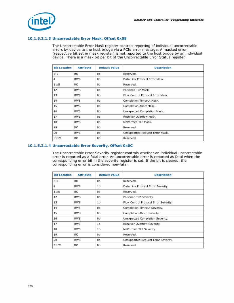
82583V GbE Controller—Programing Interface
320
10.1.5.2.1.3 Uncorrectable Error Mask, Offset 0x08
The Uncorrectable Error Mask register controls reporting of individual uncorrectable errors by device to the host bridge via a PCIe error message. A masked error (respective bit set in mask register) is not reported to the host bridge by an individual device. There is a mask bit per bit of the Uncorrectable Error Status register.
10.1.5.2.1.4 Uncorrectable Error Severity, Offset 0x0C
The Uncorrectable Error Severity register controls whether an individual uncorrectable error is reported as a fatal error. An uncorrectable error is reported as fatal when the corresponding error bit in the severity register is set. If the bit is cleared, the corresponding error is considered non-fatal.
Bit Location Attribute Default Value Description
3:0 RO 0b Reserved.
4 RWS 0b Data Link Protocol Error Mask.
11:5 RO 0b Reserved.
12 RWS 0b Poisoned TLP Mask.
13 RWS 0b Flow Control Protocol Error Mask.
14 RWS 0b Completion Timeout Mask.
15 RWS 0b Completion Abort Mask.
16 RWS 0b Unexpected Completion Mask.
17 RWS 0b Receiver Overflow Mask.
18 RWS 0b Malformed TLP Mask.
19 RO 0b Reserved.
20 RWS 0b Unsupported Request Error Mask.
31:21 RO 0b Reserved.
Bit Location Attribute Default Value Description
3:0 RO 0b Reserved.
4 RWS 1b Data Link Protocol Error Severity.
11:5 RO 0b Reserved.
12 RWS 0b Poisoned TLP Severity.
13 RWS 1b Flow Control Protocol Error Severity.
14 RWS 0b Completion Timeout Severity.
15 RWS 0b Completion Abort Severity.
16 RWS 0b Unexpected Completion Severity.
17 RWS 1b Receiver Overflow Severity.
18 RWS 1b Malformed TLP Severity.
19 RO 0b Reserved.
20 RWS 0b Unsupported Request Error Severity.
31:21 RO 0b Reserved.

321
Programing Interface—82583V GbE Controller
10.1.5.2.1.5 Correctable Error Status, Offset 0x10
The Correctable Error Status register reports error status of individual correctable error sources on a PCIe device. When an individual error status bit is set to 1b it indicates that a particular error occurred. Software might clear an error status by writing a 1b to the respective bit.
10.1.5.2.1.6 Correctable Error Mask, Offset 0x14
The Correctable Error Mask register controls reporting of individual correctable errors by device to the host bridge via a PCIe error message. A masked error (respective bit set in mask register) is not reported to the host bridge by an individual device. There is a mask bit per bit in the Correctable Error Status register.
10.1.5.2.1.7 First Error Pointer, Offset 0x18
The First Error Pointer is a read-only register that identifies the bit position of the first uncorrectable error reported in the Uncorrectable Error Status register.
Bit Location Attribute Default Value Description
0 R/W1CS 0b Receiver Error Status.
5:1 RO 0b Reserved.
6 R/W1CS 0b Bad TLP Status.
7 R/W1CS 0b Bad DLLP Status.
8 R/W1CS 0b REPLAY_NUM Rollover Status.
11:9 RO 0b Reserved.
12 R/W1CS 0b Replay Timer Timeout Status.
13 R/W1CS 0b Advisory Non Fatal Error Status.
15:14 RO 0b Reserved.
Bit Location Attribute Default Value Description
0 RWS 0b Receiver Error Mask.
5:1 RO 0b Reserved.
6 RWS 0b Bad TLP Mask.
7 RWS 0b Bad DLLP Mask.
8 RWS 0b REPLAY_NUM Rollover Mask.
11:9 RO 0b Reserved.
12 RWS 0b Replay Timer Timeout Mask.
13 RWS 1b Advisory Non Fatal Error Mask.
15:14 RO 0b Reserved.
Bit Location Attribute Default Value Description
3:0 RO 0b Vector pointing to the first recorded error in the Uncorrectable Error Status register.
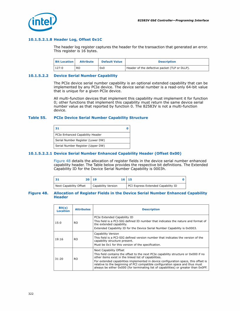
82583V GbE Controller—Programing Interface
322
10.1.5.2.1.8 Header Log, Offset 0x1C
The header log register captures the header for the transaction that generated an error. This register is 16 bytes.
10.1.5.2.2 Device Serial Number Capability
The PCIe device serial number capability is an optional extended capability that can be implemented by any PCIe device. The device serial number is a read-only 64-bit value that is unique for a given PCIe device.
All multi-function devices that implement this capability must implement it for function 0; other functions that implement this capability must return the same device serial number value as that reported by function 0. The 82583V is not a multi-function device.
Table 55. PCIe Device Serial Number Capability Structure
10.1.5.2.2.1 Device Serial Number Enhanced Capability Header (Offset 0x00)
Figure 48 details the allocation of register fields in the device serial number enhanced capability header. The Table below provides the respective bit definitions. The Extended Capability ID for the Device Serial Number Capability is 0003h.
Figure 48. Allocation of Register Fields in the Device Serial Number Enhanced Capability Header
Bit Location Attribute Default Value Description
127:0 RO 0x0 Header of the defective packet (TLP or DLLP).
31 0
PCIe Enhanced Capability Header
Serial Number Register (Lower DW)
Serial Number Register (Upper DW)
31 20 19 16 15 0
Next Capability Offset Capability Version PCI Express Extended Capability ID
Bit(s)Location Attributes Description
15:0 RO
PCIe Extended Capability IDThis field is a PCI-SIG defined ID number that indicates the nature and format of the extended capability.Extended Capability ID for the Device Serial Number Capability is 0x0003.
19:16 RO
Capability VersionThis field is a PCI-SIG defined version number that indicates the version of the capability structure present.Must be 0x1 for this version of the specification.
31:20 RO
Next Capability OffsetThis field contains the offset to the next PCIe capability structure or 0x000 if no other items exist in the linked list of capabilities.For extended capabilities implemented in device configuration space, this offset is relative to the beginning of PCI compatible configuration space and thus must always be either 0x000 (for terminating list of capabilities) or greater than 0x0FF.
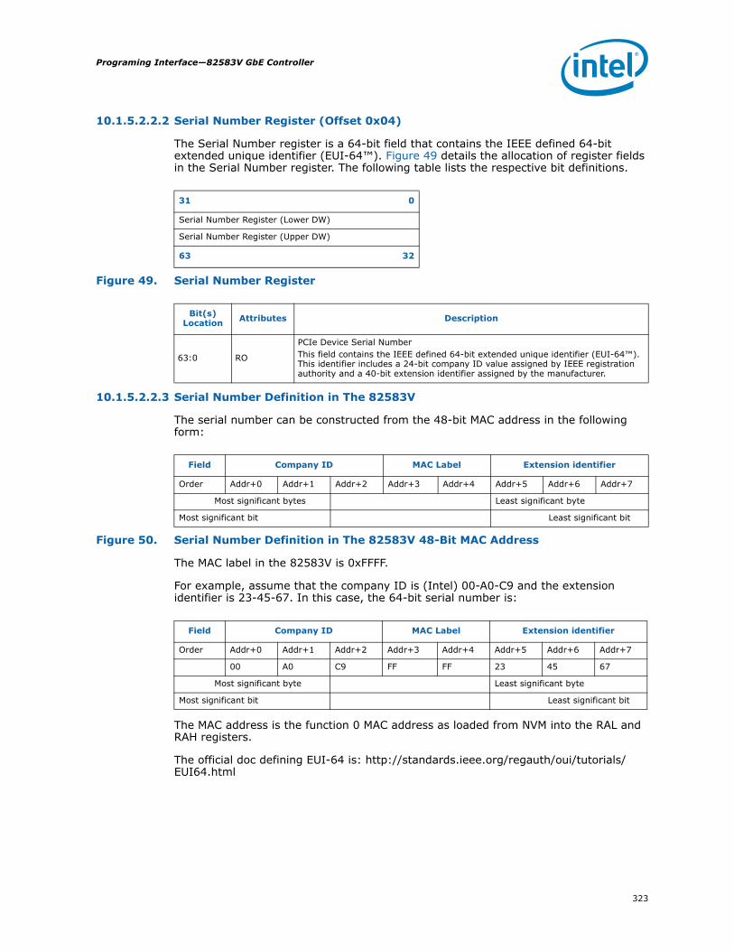
323
Programing Interface—82583V GbE Controller
10.1.5.2.2.2 Serial Number Register (Offset 0x04)
The Serial Number register is a 64-bit field that contains the IEEE defined 64-bit extended unique identifier (EUI-64™). Figure 49 details the allocation of register fields in the Serial Number register. The following table lists the respective bit definitions.
Figure 49. Serial Number Register
10.1.5.2.2.3 Serial Number Definition in The 82583V
The serial number can be constructed from the 48-bit MAC address in the following form:
Figure 50. Serial Number Definition in The 82583V 48-Bit MAC Address
The MAC label in the 82583V is 0xFFFF.
For example, assume that the company ID is (Intel) 00-A0-C9 and the extension identifier is 23-45-67. In this case, the 64-bit serial number is:
The MAC address is the function 0 MAC address as loaded from NVM into the RAL and RAH registers.
The official doc defining EUI-64 is: http://standards.ieee.org/regauth/oui/tutorials/EUI64.html
31 0
Serial Number Register (Lower DW)
Serial Number Register (Upper DW)
63 32
Bit(s)Location Attributes Description
63:0 RO
PCIe Device Serial NumberThis field contains the IEEE defined 64-bit extended unique identifier (EUI-64™). This identifier includes a 24-bit company ID value assigned by IEEE registration authority and a 40-bit extension identifier assigned by the manufacturer.
Field Company ID MAC Label Extension identifier
Order Addr+0 Addr+1 Addr+2 Addr+3 Addr+4 Addr+5 Addr+6 Addr+7
Most significant bytes Least significant byte
Most significant bit Least significant bit
Field Company ID MAC Label Extension identifier
Order Addr+0 Addr+1 Addr+2 Addr+3 Addr+4 Addr+5 Addr+6 Addr+7
00 A0 C9 FF FF 23 45 67
Most significant byte Least significant byte
Most significant bit Least significant bit

82583V GbE Controller—Design Considerations
324
11.0 Design Considerations
This section provides general design considerations and recommendations when selecting components and connecting special pins to the 82583V.
11.1 PCIe
11.1.1 Port Connection to the 82583V
PCIe is a dual simplex point-to-point serial differential low-voltage interconnect with a signaling bit rate of 2.5 Gb/s per direction. The 82583V’s PCIe port consists of an integral group of transmitters and receivers. The link between the PCIe ports of two devices is a x1 lane that also consists of a transmitter and a receiver pair. Note that each signal is 8b/10b encoded with an embedded clock.
The PCIe topology consists of a transmitter (Tx) located on one device connected through a differential pair connected to the receiver (Rx) on a second device. The 82583V can be located on a motherboard or on an add-in card using a connector specified by PCIe.
The lane is AC-coupled between its corresponding transmitter and receiver. The AC-coupling capacitor is located on the board close to transmitter side. Each end of the link is terminated on the die into nominal 100 Ω differential DC impedance. Board termination is not required.
For more information on PCIe, refer to the PCI Express* Base Specification, Revision 1.1 and PCI Express* Card Electromechanical Specification, Revision 1.1RD.
For information about the 82583V’s PCIe power management capabilities, see section 8.0.
11.1.2 PCIe Reference Clock
The 82583V uses a 100 MHz differential reference clock, denoted PECLKp and PECLKn. This signal is typically generated on the system board and routed to the PCIe port. For add-in cards, the clock is furnished at the PCIe connector.
The frequency tolerance for the PCIe reference clock is +/- 300 ppm.
11.1.3 Other PCIe Signals
The 82583V also implements other signals required by the PCIe specification. The 82583V signals power management events to the system using the PE_WAKE_N signal, which operates very similarly to the familiar PCI PME# signal. Finally, there is a PE_RST_N signal, which serves as the familiar reset function for the 82583V.

325
Design Considerations—82583V GbE Controller
11.1.4 PCIe Routing
Contact your Intel representative for information regarding the PCIe signal routing.
11.2 Clock SourceAll designs require a 25 MHz clock source. The 82583V uses the 25 MHz source to generate clocks up to 125 MHz and 1.25 GHz for the PHY circuits. For optimum results with lowest cost, connect a 25 MHz parallel resonant crystal and appropriate load capacitors at the XTAL1 and XTAL2 leads. The frequency tolerance of the timing device should be 30 ppm or better. Refer to the Intel® Ethernet Controllers Timing Device Selection Guide for more information on choosing crystals.
For further information regarding the clock for the 82583V, refer to the sections about frequency control, crystals, and oscillators that follow.
11.2.1 Frequency Control Device Design Considerations
This section provides information regarding frequency control devices, including crystals and oscillators, for use with all Intel Ethernet controllers. Several suitable frequency control devices are available; none of which present any unusual challenges in selection. The concepts documented herein are applicable to other data communication circuits, including Platform LAN Connect devices (PHYs).
The Intel Ethernet controllers contain amplifiers, which when used with the specific external components, form the basis for feedback oscillators. These oscillator circuits, which are both economical and reliable, are described in more detail in section 11.3.1.
The Intel Ethernet controllers also have bus clock input functionality, however a discussion of this feature is beyond the scope of this document, and will not be addressed.
The chosen frequency control device vendor should be consulted early in the design cycle. Crystal and oscillator manufacturers familiar with networking equipment clock requirements may provide assistance in selecting an optimum, low-cost solution.
11.2.2 Frequency Control Component Types
Several types of third-party frequency reference components are currently marketed. A discussion of each follows, listed in preferred order.
11.2.2.1 Quartz Crystal
Quartz crystals are generally considered to be the mainstay of frequency control components due to their low cost and ease of implementation. They are available from numerous vendors in many package types and with various specification options.
11.2.2.2 Fixed Crystal Oscillator
A packaged fixed crystal oscillator comprises an inverter, a quartz crystal, and passive components conveniently packaged together. The device renders a strong, consistent square wave output. Oscillators used with microprocessors are supplied in many configurations and tolerances.
Crystal oscillators should be restricted to use in special situations, such as shared clocking among devices or multiple controllers. As clock routing can be difficult to accomplish, it is preferable to provide a separate crystal for each device.

82583V GbE Controller—Design Considerations
326
11.2.2.3 Programmable Crystal Oscillators
A programmable oscillator can be configured to operate at many frequencies. The device contains a crystal frequency reference and a phase lock loop (PLL) clock generator. The frequency multipliers and divisors are controlled by programmable fuses.
A programmable oscillator’s accuracy depends heavily on the Ethernet device’s differential transmit lines. The Physical Layer (PHY) uses the clock input from the device to drive a differential Manchester (for 10 Mb/s operation), an MLT-3 (for 100 Mbps operation) or a PAM-5 (for 1000 Mbps operation) encoded analog signal across the twisted pair cable. These signals are referred to as self-clocking, which means the clock must be recovered at the receiving link partner. Clock recovery is performed with another PLL that locks onto the signal at the other end.
PLLs are prone to exhibit frequency jitter. The transmitted signal can also have considerable jitter even with the programmable oscillator working within its specified frequency tolerance. PLLs must be designed carefully to lock onto signals over a reasonable frequency range. If the transmitted signal has high jitter and the receiver’s PLL loses its lock, then bit errors or link loss can occur.
PHY devices are deployed for many different communication applications. Some PHYs contain PLLs with marginal lock range and cannot tolerate the jitter inherent in data transmission clocked with a programmable oscillator. The American National Standards Institute (ANSI) X3.263-1995 standard test method for transmit jitter is not stringent enough to predict PLL-to-PLL lock failures, therefore, the use of programmable oscillators is not recommended.
11.2.2.4 Ceramic Resonator
Similar to a quartz crystal, a ceramic resonator is a piezoelectric device. A ceramic resonator typically carries a frequency tolerance of ±0.5%, – inadequate for use with Intel Ethernet controllers, and therefore, should not be utilized.

327
Design Considerations—82583V GbE Controller
11.3 Crystal Support
11.3.1 Crystal Selection Parameters
All crystals used with Intel Ethernet controllers are described as AT-cut, which refers to the angle at which the unit is sliced with respect to the long axis of the quartz stone. Table 56 lists crystals which have been used successfully in other designs (however, no particular product is recommended):
For information about crystal selection parameters, see section 11.7 and Table 18.
11.3.1.1 Vibrational Mode
Crystals in the above-referenced frequency range are available in both fundamental and third overtone. Unless there is a special need for third overtone, use fundamental mode crystals.
At any given operating frequency, third overtone crystals are thicker and more rugged than fundamental mode crystals. Third overtone crystals are more suitable for use in military or harsh industrial environments. Third overtone crystals require a trap circuit (extra capacitor and inductor) in the load circuitry to suppress fundamental mode oscillation as the circuit powers up. Selecting values for these components is beyond the scope of this document.
11.3.1.2 Nominal Frequency
Intel Ethernet controllers use a crystal frequency of 25.000 MHz. The 25 MHz input is used to generate a 125 MHz transmit clock for 100BASE-TX and 1000BASE-TX operation – 10 MHz and 20 MHz transmit clocks, for 10BASE-T operation.
11.3.1.3 Frequency Tolerance
The frequency tolerance for an Ethernet Platform LAN Connect is dictated by the IEEE 802.3 specification as ±50 parts per million (ppm). This measurement is referenced to a standard temperature of 25° C. Intel recommends a frequency tolerance of ±30 ppm.
11.3.1.4 Temperature Stability and Environmental Requirements
Temperature stability is a standard measure of how the oscillation frequency varies over the full operational temperature range (and beyond). Some vendors separate operating temperatures from temperature stability. Manufacturers may also list temperature stability as 50 ppm in their data sheets.
Note: Crystals also carry other specifications for storage temperature, shock resistance, and reflow solder conditions. Crystal vendors should be consulted early in the design cycle to discuss the application and its environmental requirements.
Table 56. Crystal Manufacturers and Part Numbers
Manufacturer Part No.
KDS America DSX321G
NDK America Inc. 41CD25.0F1303018
TXC Corporation - USA7A250001659C25000008

82583V GbE Controller—Design Considerations
328
11.3.1.5 Crystal Oscillation Mode
The terms series-resonant and parallel-resonant are often used to describe crystal oscillator circuits. Specifying parallel mode is critical to determining how the crystal frequency is calibrated at the factory.
A crystal specified and tested as series resonant oscillates without problem in a parallel-resonant circuit, but the frequency is higher than nominal by several hundred parts per million. The purpose of adding load capacitors to a crystal oscillator circuit is to establish resonance at a frequency higher than the crystal’s inherent series resonant frequency.
Figure 51 shows the recommended placement and layout of an internal oscillator circuit. Note that pin X1 and X2 refers to XTAL1 and XTAL2 in the Ethernet device, respectively. The crystal and the capacitors form a feedback element for the internal inverting amplifier. This combination is called parallel-resonant, because it has positive reactance at the selected frequency. In other words, the crystal behaves like an inductor in a parallel LC circuit. Oscillators with piezoelectric feedback elements are also known as “Pierce” oscillators.
11.3.1.6 Load Capacitance and Discrete Capacitors
The formula for crystal load capacitance is as follows:
where:
CL is the rated Cload of the crystal component and C1 and C2 are discrete crystal circuit capacitors.Cstray allows for additional capacitance from solder pads, traces and the 82583V package. Individual stray capacitance components can be estimated and added as parallel capacitances. Note that total Cstray is typically 3 pF to 7 pF.
Solve for the discrete capacitor values as follows:C1 = C2 = 2 * [Cload - Cstray]
For example:
If total Cstray = 4.0 pF and if the Cload rating is 18 pF, then the calculated C1 and C2 = 2 * [18 pF - 4.0 pF] = 28 pF.
Note: Because 28 pF is not a standard value, use 27 pF capacitors for C1 and C2, which is the closest standard value.
The oscillator frequency should be measured with a precision frequency counter where possible. The values of C1 and C2 should be fine tuned for the design. As the actual capacitive load increases, the oscillator frequency decreases.
Note: Intel recommends COG or NPO capacitors with a tolerance of ±5% (approximately ±1 pF) or smaller.
CLC1 C2⋅( )C1 C2+( )
------------------- Cstray+=
329
Design Considerations—82583V GbE Controller
11.3.1.7 Shunt Capacitance
The shunt capacitance parameter is relatively unimportant compared to load capacitance. Shunt capacitance represents the effect of the crystal’s mechanical holder and contacts. The shunt capacitance should equal a maximum of 6 pF.
11.3.1.8 Equivalent Series Resistance
Equivalent Series Resistance (ESR) is the real component of the crystal’s impedance at the calibration frequency, which the inverting amplifier’s loop gain must overcome. ESR varies inversely with frequency for a given crystal family. The lower the ESR, the faster the crystal starts up. Use crystals with an ESR value of 50 Ω or better.
11.3.1.9 Drive Level
Drive level refers to power dissipation in use. The allowable drive level for a Surface Mounted Technology (SMT) crystal is less than its through-hole counterpart, because surface mount crystals are typically made from narrow, rectangular AT strips, rather than circular AT quartz blanks.
Some crystal data sheets list crystals with a maximum drive level of 1 mW. However, Intel Ethernet controllers drive crystals to a level less than the suggested 0.3 mW value. This parameter does not have much value for on-chip oscillator use.
11.3.1.10 Aging
Aging is a permanent change in frequency (and resistance) occurring over time. This parameter is most important in its first year because new crystals age faster than old crystals. Use crystals with a maximum of ±5 ppm per year aging.
11.3.1.11 Reference Crystal
The normal tolerances of the discrete crystal components can contribute to small frequency offsets with respect to the target center frequency. To minimize the risk of tolerance-caused frequency offsets causing a small percentage of production line units to be outside of the acceptable frequency range, it is important to account for those shifts while empirically determining the proper values for the discrete loading capacitors, C1 and C2.
Even with a perfect support circuit, most crystals will oscillate slightly higher or slightly lower than the exact center of the target frequency. Therefore, frequency measurements (which determine the correct value for C1 and C2) should be performed with an ideal reference crystal. When the capacitive load is exactly equal to the crystal’s load rating, an ideal reference crystal will be perfectly centered at the desired target frequency.
11.3.1.11.1 Reference Crystal Selection
There are several methods available for choosing the appropriate reference crystal:• If a Saunders and Associates (S&A) crystal network analyzer is available, then
discrete crystal components can be tested until one is found with zero or nearly zero ppm deviation (with the appropriate capacitive load). A crystal with zero or near zero ppm deviation will be a good reference crystal to use in subsequent frequency tests to determine the best values for C1 and C2.

82583V GbE Controller—Design Considerations
330
• If a crystal analyzer is not available, then the selection of a reference crystal can be done by measuring a statistically valid sample population of crystals, which has units from multiple lots and approved vendors. The crystal, which has an oscillation frequency closest to the center of the distribution, should be the reference crystal used during testing to determine the best values for C1 and C2.
• It may also be possible to ask the approved crystal vendors or manufacturers to provide a reference crystal with zero or nearly zero deviation from the specified frequency when it has the specified CLoad capacitance.
When choosing a crystal, customers must keep in mind that to comply with IEEE specifications for 10/100 and 10/100/1000Base-T Ethernet LAN, the transmitter reference frequency must be precise within ±50 ppm. Intel® recommends customers to use a transmitter reference frequency that is accurate to within ±30 ppm to account for variations in crystal accuracy due to crystal manufacturing tolerance.
11.3.1.11.2 Circuit Board
Since the dielectric layers of the circuit board are allowed some reasonable variation in thickness, the stray capacitance from the printed board (to the crystal circuit) will also vary. If the thickness tolerance for the outer layers of dielectric are controlled within ±17 percent of nominal, then the circuit board should not cause more than ±2 pF variation to the stray capacitance at the crystal. When tuning crystal frequency, it is recommended that at least three circuit boards are tested for frequency. These boards should be from different production lots of bare circuit boards.
Alternatively, a larger sample population of circuit boards can be used. A larger population will increase the probability of obtaining the full range of possible variations in dielectric thickness and the full range of variation in stray capacitance.
Next, the exact same crystal and discrete load capacitors (C1 and C2) must be soldered onto each board, and the LAN reference frequency should be measured on each circuit board.
The circuit board, which has a LAN reference frequency closest to the center of the frequency distribution, should be used while performing the frequency measurements to select the appropriate value for C1 and C2.
11.3.1.11.3 Temperature Changes
Temperature changes can cause the crystal frequency to shift. Therefore, frequency measurements should be done in the final system chassis across the system’s rated operating temperature range.
11.3.2 Crystal Placement and Layout Recommendations
Crystal clock sources should not be placed near I/O ports or board edges. Radiation from these devices can be coupled into the I/O ports and radiate beyond the system chassis. Crystals should also be kept away from the Ethernet magnetics module to prevent interference.
Note: Failure to follow these guidelines could result in the 25 MHz clock failing to start.
When designing the layout for the crystal circuit, the following rules must be used:• Place load capacitors as close as possible (within design-for-manufacturability
rules) to the crystal solder pads. They should be no more than 90 mils away from crystal pads.
• The two load capacitors, crystal component, the Ethernet controller device, and the crystal circuit traces must all be located on the same side of the circuit board (maximum of one via-to-ground load capacitor on each XTAL trace).

331
Design Considerations—82583V GbE Controller
• Use 27 pF (5% tolerance) 0402 load capacitors. • Place load capacitor solder pad directly in line with circuit trace (see Figure 51,
point A).• Use 50 Ω impedance single-ended microstrip traces for the crystal circuit. • Route traces so that electro-magnetic fields from XTAL2 do not couple onto XTAL1.
No differential traces.• Route XTAL1 and XTAL2 traces to nearest inside corners of crystal pad (see
Figure 51, point B).• Ensure that the traces from XTAL1 and XTAL2 are symmetrically routed and that
their lengths are matched. • The total trace length of XTAL1 or XTAL2 should be less than 750 mils.
Figure 51. Recommended Crystal Placement and Layout
11.4 Oscillator SupportThe 82583V clock input circuit is optimized for use with an external crystal. However, an oscillator can also be used in place of the crystal with the proper design considerations (see Table 19 for detailed clock oscillator specifications):
• The clock oscillator has an internal voltage regulator of 1.9 V dc to isolate it from the external noise of other circuits to minimize jitter. If an external clock is used, this imposes a maximum input clock amplitude of 1.9 V dc. For example, if a 3.3 V dc oscillator is used, it's signal should be attenuated to a maximum of 1.9 V dc with a resistive divider circuit.
Crystal Pad Crystal Pad
Ethernet Controller
Xtal1Xtal2
27pF0402
27pF0402
Crystal
“B” “B”
“A”
90
mils
90 m
ils
Capacitor Capacitor
Less than 660 mils

82583V GbE Controller—Design Considerations
332
• The input capacitance introduced by the 82583V (approximately 20 pF) is greater than the capacitance specified by a typical oscillator (approximately 15 pF).
• The input clock jitter from the oscillator can impact the 82583V clock and its performance.
Note: The power consumption of additional circuitry equals about 1.5 mW.
Table 57 lists oscillators that can be used with the 82583V. Please note that no particular oscillator is recommended):
Figure 52. Oscillator Solution
11.4.1 Oscillator Placement and Layout Recommendations
Oscillator clock sources should not be placed near I/O ports or board edges. Radiation from these devices can be coupled into the I/O ports and radiate beyond the system chassis. Oscillators should also be kept away from the Ethernet magnetics module to prevent interference.
Table 57. Oscillator Manufacturers and Part Numbers
Manufacturer Part No.
NDK AMERICA INC 2560TKA-25M
TXC CORPORATION - USA 6N25000160 or 7W25000025
CITIZEN AMERICA CORP CSX750FJB25.000M-UT
Raltron Electronics Corp CO4305-25.000-T-TR
MtronPTI M214TCN
Kyocera Corporation KC5032C-C3
3.3 V dc
C1
VDD3p3
1 K ohm
Out1 K ohm 1000 pF
CLKOscillator 82583V
XTAL1

333
Design Considerations—82583V GbE Controller
11.5 Ethernet Interface
11.5.1 Magnetics for 1000 BASE-T
Magnetics for the 82583V can be either integrated or discrete.
The magnetics module has a critical effect on overall IEEE and emissions conformance. The device should meet the performance required for a design with reasonable margin to allow for manufacturing variation. Occasionally, components that meet basic specifications can cause the system to fail IEEE testing because of interactions with other components or the printed circuit board itself. Carefully qualifying new magnetics modules prevents this problem.
When using discrete magnetics it is necessary to use Bob Smith termination: Use four 75 Ω resistors for cable-side center taps and unused pins. This method terminates pair-to-pair common mode impedance of the CAT5 cable.
Use an EFT capacitor attached to the termination plane. Suggested values are 1500 pF/2 KV or 1000 pF/3 KV. A minimum of 50-mil spacing from capacitor to traces and components should be maintained.
11.5.2 Magnetics Module Qualification Steps
The steps involved in magnetics module qualification are similar to those for crystal qualification:1. Verify that the vendor’s published specifications in the component datasheet meet
or exceed the specifications in section 11.6.2. Independently measure the component’s electrical parameters on the test bench,
checking samples from multiple lots. Check that the measured behavior is consistent from sample to sample and that measurements meet the published specifications.
3. Perform physical layer conformance testing and EMC (FCC and EN) testing in real systems. Vary temperature and voltage while performing system level tests.
11.5.3 Third-Party Magnetics Manufacturers
The following magnetics modules have been used successfully in previous designs.
Manufacturer Part Number
Low Profile Discrete:Midcom Inc. 000-7412-35R-LF1
Standard Discrete:BelFusePulse Eng.
S558-5999-P3 (12-core)H5007NL (12-core)
Integrated:FOXCONNPulse Eng.AmphenolBelFuseTyco
JFM38U1C-L1U1WJW0-0013NLRJMG2310 22830ER C03-0020862-1J1T-Z4-F6368472-1

82583V GbE Controller—Design Considerations
334
11.5.4 Designing the 82583V as a 10/100 Mb/s Only Device
To connect the 82583V as a 10/100 Mb/s only device:1. Set bit 14 of the LED 1 Configuration Defaults/PHY Configuration (Word 0x1C) to
1b. Setting bit 14 to 1b disables 1000 Mb/s operation in all power modes (see section 6.1.1.18).
2. Connect MDI pair 0 (pins 57 and 58) and MDI pair 1 (pins 54 and 55) to your magnetics. MDI pair 2 (pins 52 and 53) and MDI pair 3 (pins 49 and 50) can each be pulled up to 1.9 V dc through a 50 Ω resistor or connected to the magnetics as a gigabit device if it is desired at a later time to enable gigabit by altering bit 14 of the LED 1 Configuration Defaults/PHY Configuration; word 0x1C (Giga Disable). See Figure 53 and Figure 54 for details.
3. Use one of the approved discrete gigabit magnetics that were tested with the 82583V (refer to section 11.5.3). Note that Intel has not tested any 10/100 magnetics with the 82583V.
Note: If you must use 10/100 magnetics in your design with the 82583V, the magnetics must have a Common Mode Choke (CMC) in the receive path.
The 82583V supports auto-MDIX; this feature CANNOT be disabled. If there is no CMC in the receive path, the system most likely will not pass regulatory radiated emission tests when MDI-X mode is used.
Figure 53. 82583V Gigabit Magnetics Module Connections
82583V
M DI_PLUS (0 )
M D I_M INU S (0)
M DI_PLUS (1 )
M D I_M INU S (1)
57
58
54
55
M DI_PLUS (2 )
M D I_M INU S (2)
M DI_PLUS (3 )
M D I_M INU S (3)
52
53
49
50
G igabit M agneticsM odule

335
Design Considerations—82583V GbE Controller
Figure 54. 82583V 10/100 Mb/s Magnetics Module Connections (With CMC)
11.5.5 Layout Considerations for the Ethernet Interface
These sections provide recommendations for performing printed circuit board layouts. Good layout practices are essential to meet IEEE PHY conformance specifications and EMI regulatory requirements.
Critical signal traces should be kept as short as possible to decrease the likelihood of being affected by high frequency noise from other signals, including noise carried on power and ground planes. Keeping the traces as short as possible can also reduce capacitive loading.
Since the transmission line medium extends onto the printed circuit board, special attention must be paid to layout and routing of the differential signal pairs.
Designing for 1000 BASE-T Gigabit operation is very similar to designing for 10 and 100 Mb/s. For the 82583V, system level tests should be performed at all three speeds.
11.5.5.1 Guidelines for Component Placement
Component placement can affect signal quality, emissions, and component operating temperature This section provides guidelines for component placement.
Careful component placement can:• Decrease potential problems directly related to electromagnetic interference (EMI),
which could cause failure to meet applicable government test specifications.• Simplify the task of routing traces. To some extent, component orientation will
affect the complexity of trace routing. The overall objective is to minimize turns and crossovers between traces.
82583V
M D I_PLU S (0)
M DI_M IN US (0 )
M D I_PLU S (1)
M DI_M IN US (1 )
57
58
54
55
M D I_PLU S (2)
M DI_M IN US (2 )
M D I_PLU S (3)
M DI_M IN US (3 )
52
53
49
50
LAN_1.9V
10 /100 M agneticsM odule w ith Com m on M ode
Choke in Both R x and Tx Paths 50 O hm
R esistors

82583V GbE Controller—Design Considerations
336
Minimizing the amount of space needed for the Ethernet LAN interface is important because other interfaces compete for physical space on a motherboard near the connector. The Ethernet LAN circuits need to be as close as possible to the connector.
Figure 55. General Placement Distances for 1000 BASE-T Designs
Figure 55 shows some basic placement distance guidelines. Figure 55 shows two differential pairs, but can be generalized for a Gigabit system with four analog pairs. The ideal placement for the Ethernet silicon would be approximately one inch behind the magnetics module.
While it is generally a good idea to minimize lengths and distances, Figure 55 also illustrates the need to keep the LAN silicon away from the edge of the board and the magnetics module for best EMI performance.
11.5.5.2 Layout Guidelines for Use with Integrated and Discrete Magnetics
Layout requirements are slightly different when using discrete magnetics.
These include:• Ground cut for HV installation (not required for integrated magnetics)• A maximum of two (2) vias• Turns less than 45°• Discrete terminators
Figure 56 shows a reference layout for discrete magnetics.
LANSilicon
IntegratedRJ-45w/LAN
MagneticsKeep LAN silicon 1" - 4" from LAN connector.
Keep silicon traces at least 1" from edge ofPB (2" is preferred).
Keep minimum distance between differential pairs more than seven times the dielectric thickness away from each other and other traces, including NVM traces and parallel digital traces.
Note: Figure 55 represents a 10/100 diagram. Use the same design considerations for the twodifferential pairs not shown for gigabit implementations.

337
Design Considerations—82583V GbE Controller
Figure 56. Layout for Discrete Magnetics
11.5.5.3 Board Stack-Up Recommendations
Printed circuit boards for these designs typically have four, six, eight, or more layers. Although, the 82583V does not dictate the stack up, here is an example of a typical six-layer board stack up:
• Layer 1 is a signal layer. It can contain the differential analog pairs from the Ethernet device to the magnetics module.
• Layer 2 is a signal ground layer. Chassis ground may also be fabricated in Layer 2 under the connector side of the magnetics module.
• Layer 3 is used for power planes.• Layer 4 is a signal layer. • Layer 5 is an additional ground layer.• Layer 6 is a signal layer. For 1000 BASE-T (copper) Gigabit designs, it is common to
route two of the differential pairs (per port) on this layer.
This board stack up configuration can be adjusted to conform to specific OEM design rules.
RJ-45
82583V
Magnetics Module

82583V GbE Controller—Design Considerations
338
11.5.5.4 Differential Pair Trace Routing for 10/100/1000 Designs
Trace routing considerations are important to minimize the effects of crosstalk and propagation delays on sections of the board where high-speed signals exist. Signal traces should be kept as short as possible to decrease interference from other signals, including those propagated through power and ground planes. Observe the following suggestions to help optimize board performance:
• Maintain constant symmetry and spacing between the traces within a differential pair.
• Minimize the difference in signal trace lengths of a differential pair.• Keep the total length of each differential pair under 4 inches. Although possible,
designs with differential traces longer than 5 inches are much more likely to have degraded receive BER (Bit Error Rate) performance, IEEE PHY conformance failures, and/or excessive EMI (Electromagnetic Interference) radiation.
• Keep differential pairs more than seven times the dielectric thickness away from each other and other traces, including NVM traces and parallel digital traces.
• Keep maximum separation within differential pairs to 7 mils. • For high-speed signals, the number of corners and vias should be kept to a
minimum. If a 90° bend is required, it is recommended to use two 45° bends instead. Refer to Figure 57.
Note: In manufacturing, vias are required for testing and troubleshooting purposes. The via size should be a 17-mil (±2 mils for manufacturing variance) finished hole size (FHS).
• Traces should be routed away from board edges by a distance greater than the trace height above the reference plane. This allows the field around the trace to couple more easily to the ground plane rather than to adjacent wires or boards.
• Do not route traces and vias under crystals or oscillators. This will prevent coupling to or from the clock. And as a general rule, place traces from clocks and drives at a minimum distance from apertures by a distance that is greater than the largest aperture dimension
.
Figure 57. Trace Routing• The reference plane for the differential pairs should be continuous and low
impedance. It is recommended that the reference plane be either ground or 1.9 V dc (the voltage used by the PHY). This provides an adequate return path for and high frequency noise currents.
• Do not route differential pairs over splits in the associated reference plane as it may cause discontinuity in impedances.
45°
45°
339
Design Considerations—82583V GbE Controller
11.5.5.5 Signal Termination and Coupling
The 82547L has internal termination on the MDI signals. External resistors are not needed. Adding pads for external resistors can degrade signal integrity.
11.5.5.6 Signal Trace Geometry for 1000 BASE-T Designs
The key factors in controlling trace EMI radiation are the trace length and the ratio of trace-width to trace-height above the reference plane. To minimize trace inductance, high-speed signals and signal layers that are close to a reference or power plane should be as short and wide as practical. Ideally, this trace width to height above the ground plane ratio is between 1:1 and 3:1. To maintain trace impedance, the width of the trace should be modified when changing from one board layer to another if the two layers are not equidistant from the neighboring planes.
Each pair of signal should have a differential impedance of 100 Ω. +/- 15%. If a particular tool cannot design differential traces, it is permissible to specify 55-65 Ω single-ended traces as long as the spacing between the two traces is minimized. As an example, consider a differential trace pair on Layer 1 that is 8 mils (0.2 mm) wide and 2 mils (0.05 mm) thick, with a spacing of 8 mils (0.2 mm). If the fiberglass layer is 8 mils (0.2 mm) thick with a dielectric constant, ER, of 4.7, the calculated single-ended impedance would be approximately 61 Ω and the calculated differential impedance would be approximately 100 Ω.
When performing a board layout, do not allow the CAD tool auto-router to route the differential pairs without intervention. In most cases, the differential pairs will have to be routed manually.
Note: Measuring trace impedance for layout designs targeting 100 Ω often results in lower actual impedance. Designers should verify actual trace impedance and adjust the layout accordingly. If the actual impedance is consistently low, a target of 105 – 110 Ω should compensate for second order effects.
It is necessary to compensate for trace-to-trace edge coupling, which can lower the differential impedance by up to 10 Ω, when the traces within a pair are closer than 30 mils (edge to edge).
11.5.5.7 Trace Length and Symmetry for 1000 BASE-T Designs
As indicated earlier, the overall length of differential pairs should be less than four inches measured from the Ethernet device to the magnetics.
The differential traces (within each pair) should be equal in total length to within 50 mils (1.25 mm) and as symmetrical as possible. Asymmetrical and unequal length traces in the differential pairs contribute to common mode noise. If a choice has to be made between matching lengths and fixing symmetry, more emphasis should be placed on fixing symmetry. Common mode noise can degrade the receive circuit’s performance and contribute to radiated emissions.
11.5.5.8 Routing 1.9 V dc to the Magnetics Center Tap
The central-tap 1.9 V dc should be delivered as a solid supply plane (1.9 V dc) directly to the magnetic module or, if this is not possible, by a short and thick trace (lower than 0.2 Ω DC resistance). The decoupling capacitors for the central tap pins should be placed as close as possible to the magnetic component. This improves both EMI and IEEE compliance.

82583V GbE Controller—Design Considerations
340
11.5.5.9 Impedance Discontinuities
Impedance discontinuities cause unwanted signal reflections. Minimize vias (signal through holes) and other transmission line irregularities. If vias must be used, a reasonable budget is two per differential trace. Unused pads and stub traces should also be avoided.
11.5.5.10 Reducing Circuit Inductance
Traces should be routed over a continuous reference plane with no interruptions. If there are vacant areas on a reference or power plane, the signal conductors should not cross the vacant area. This causes impedance mismatches and associated radiated noise levels. Noisy logic grounds should be separated from analog signal grounds to reduce coupling. Noisy logic grounds can sometimes affect sensitive DC subsystems such as analog to digital conversion, operational amplifiers, etc. All ground vias should be connected to every ground plane; and similarly, every power via, to all power planes at equal potential. This helps reduce circuit inductance. Another recommendation is to physically locate grounds to minimize the loop area between a signal path and its return path. Rise and fall times should be as slow as possible. Because signals with fast rise and fall times contain many high frequency harmonics, which can radiate significantly. The most sensitive signal returns closest to the chassis ground should be connected together. This will result in a smaller loop area and reduce the likelihood of crosstalk. The effect of different configurations on the amount of crosstalk can be studied using electronics modeling software.
11.5.5.11 Signal Isolation
To maintain best signal integrity, keep digital signals far away from the analog traces. A good rule of thumb is no digital signal should be within 300 mils (7.5 mm) of the differential pairs. If digital signals on other board layers cannot be separated by a ground plane, they should be routed perpendicular to the differential pairs. If there is another LAN controller on the board, take care to keep the differential pairs from that circuit away.
Some rules to follow for signal isolation:• Separate and group signals by function on separate layers if possible. Keep a
minimum distance between differential pairs more than seven times the dielectric thickness away from each other and other traces, including NVM traces and parallel digital traces.
• Physically group together all components associated with one clock trace to reduce trace length and radiation.
• Isolate I/O signals from high-speed signals to minimize crosstalk, which can increase EMI emission and susceptibility to EMI from other signals.
• Avoid routing high-speed LAN traces near other high-frequency signals associated with a video controller, cache controller, processor, or other similar devices.
11.5.5.12 Traces for Decoupling Capacitors
Traces between decoupling and I/O filter capacitors should be as short and wide as practical. Long and thin traces are more inductive and would reduce the intended effect of decoupling capacitors. Also for similar reasons, traces to I/O signals and signal terminations should be as short as possible. Vias to the decoupling capacitors should be sufficiently large in diameter to decrease series inductance.

341
Design Considerations—82583V GbE Controller
11.5.5.13 Light Emitting Diodes for Designs Based on the 82583V
The 82583V provides three programmable high-current push-pull (active high) outputs to directly drive LEDs for link activity and speed indication. Each LAN device provides an independent set of LED outputs; these pins and their function are bound to a specific LAN device. Each of the four LED outputs can be individually configured to select the particular event, state, or activity, which is indicated on that output. In addition, each LED can be individually configured for output polarity, as well as for blinking versus non-blinking (steady-state) indication.
Since the LEDs are likely to be integral to a magnetics module, take care to route the LED traces away from potential sources of EMI noise. In some cases, it may be desirable to attach filter capacitors.
The LED ports are fully programmable through the NVM interface.
11.5.6 Physical Layer Conformance Testing
Physical layer conformance testing (also known as IEEE testing) is a fundamental capability for all companies with Ethernet LAN products. PHY testing is the final determination that a layout has been performed successfully. If your company does not have the resources and equipment to perform these tests, consider contracting the tests to an outside facility.
11.5.6.1 Conformance Tests for 10/100/1000 Mb/s Designs
Crucial tests are as follows, listed in priority order: • Bit Error Rate (BER). Good indicator of real world network performance. Perform bit
error rate testing with long and short cables and many link partners. The test limit is 10-11 errors.
• Output Amplitude, Rise and Fall Time (10/100 Mb/s), Symmetry and Droop (1000Mbps). For the 82575 controller, use the appropriate PHY test waveform.
• Return Loss. Indicator of proper impedance matching, measured through the RJ-45 connector back toward the magnetics module.
• Jitter Test (10/100 Mb/s) or Unfiltered Jitter Test (1000 Mb/s). Indicator of clock recovery ability (master and slave for Gigabit controller).
11.5.7 Troubleshooting Common Physical Layout Issues
The following is a list of common physical layer design and layout mistakes in LAN On Motherboard Designs.1. Lack of symmetry between the two traces within a differential pair. Asymmetry can
create common-mode noise and distort the waveforms. For each component and/or via that one trace encounters, the other trace should encounter the same component or a via at the same distance from the Ethernet silicon.
2. Unequal length of the two traces within a differential pair. Inequalities create common-mode noise and will distort the transmit or receive waveforms.
3. Excessive distance between the Ethernet silicon and the magnetics. Long traces on FR4 fiberglass epoxy substrate will attenuate the analog signals. In addition, any impedance mismatch in the traces will be aggravated if they are longer than the four inch guideline.

82583V GbE Controller—Design Considerations
342
4. Routing any other trace parallel to and close to one of the differential traces. Crosstalk getting onto the receive channel will cause degraded long cable BER. Crosstalk getting onto the transmit channel can cause excessive EMI emissions and can cause poor transmit BER on long cables. At a minimum, other signals should be kept 0.3 inches from the differential traces.
5. Routing one pair of differential traces too close to another pair of differential traces. After exiting the Ethernet silicon, the trace pairs should be kept 0.3 inches or more away from the other trace pairs. The only possible exceptions are in the vicinities where the traces enter or exit the magnetics, the RJ-45 connector, and the Ethernet silicon.
6. Use of a low-quality magnetics module. 7. Re-use of an out-of-date physical layer schematic in a Ethernet silicon design. The
terminations and decoupling can be different from one PHY to another.8. Incorrect differential trace impedances. It is important to have ~100 Ω impedance
between the two traces within a differential pair. This becomes even more important as the differential traces become longer. To calculate differential impedance, many impedance calculators only multiply the single-ended impedance by two. This does not take into account edge-to-edge capacitive coupling between the two traces. When the two traces within a differential pair are kept close to each other, the edge coupling can lower the effective differential impedance by 5 Ω to 20 Ω. Short traces have fewer problems if the differential impedance is slightly off target.
11.6 82583V Power SuppliesThe 82583V requires three power rails: 3.3 V dc, 1.9 V dc, and 1.05 V dc (see section 8.4). A central power supply can provide all the required voltage sources or the power can be derived from the 3.3 V dc supply and regulated locally using external regulators. If the LAN wake capability is used, all voltages must remain present during system power down. Local regulation of the LAN voltages from system 3.3 Vmain and 3.3 Vaux voltages is recommended. Refer to section 11.3 and section 11.5 for detailed information about power supply sequencing rules and intended design options for power solutions.
External voltage regulators need to generate the proper voltage, supply current requirements (with adequate margin), and provide the proper power sequencing.
11.6.1 82583V GbE Controller Power Sequencing
Designs must comply with power sequencing requirements to avoid latch-up and forward-biased internal diodes (see Figure 58).
The general guideline for sequencing is: 1. Power up the 3.3 V dc rail.2. Power up the 1.9 V dc next.3. Power up the 1.05 V dc rail last.
For power down, there is no requirement (only charge that remains is stored in the decoupling capacitors).

343
Design Considerations—82583V GbE Controller
Figure 58. Power Sequencing Guideline
11.6.1.1 Power Up Sequence (External LVR)
The board designer controls the power up sequence with the following stipulations (see Figure 59):
• 1.9 V dc must not exceed 3.3 V dc by more than 0.3 V dc.• 1.05 V dc must not exceed 1.9 V dc by more than 0.3 V dc.• 1.05 V dc must not exceed 3.3 V dc by more than 0.3 V dc.
Figure 59. External LVR Power-up Sequence
VDD3p3
AVDD1p9
VDD1p0
VDD3p3
AVDD1p9
VDD1p0

82583V GbE Controller—Design Considerations
344
11.6.1.2 Power Up-Sequence (Internal LVR)
The 82583V controls the power-up sequence internally and automatically with the following conditions (see Figure 60):
• 3.3 V dc must be the source for the internal LVR.• 1.9 V dc never exceeds 3.3 V dc.• 1.05 V dc never exceeds 3.3 V dc or 1.9 V dc.
The ramp is delayed internally, with Tdelay depending on the rising slope of the 3.3 V dc ramp.
Figure 60. Internal LVR Power-Up Sequence
11.6.2 Power and Ground Planes
Good grounding requires minimizing inductance levels in the interconnections and keeping ground returns short, signal loop areas small, and power inputs bypassed to signal return, will significantly reduce EMI radiation.
The following guidelines help reduce circuit inductance in both backplanes and motherboards:
• Route traces over a continuous plane with no interruptions. Do not route over a split power or ground plane. If there are vacant areas on a ground or power plane, avoid routing signals over the vacant area. This will increase inductance and EMI radiation levels.
• Separate noisy digital grounds from analog grounds to reduce coupling. Noisy digital grounds may affect sensitive DC subsystems.
• All ground vias should be connected to every ground plane; and every power via should be connected to all power planes at equal potential. This helps reduce circuit inductance.
• Physically locate grounds between a signal path and its return. This will minimize the loop area.
• Avoid fast rise/fall times as much as possible. Signals with fast rise and fall times contain many high frequency harmonics, which can radiate EMI.
AVDD1p9
VDD1p0
VDD3p3

345
Design Considerations—82583V GbE Controller
• The ground plane beneath a magnetics module should be split. The RJ45 connector side of the transformer module should have chassis ground beneath it.
• Power delivery traces should be a minimum of 100 mils wide at all places from the source to the destination. As power flows through pass transistors or regulators, the traces must be kept wide as well. The distribution of power is better done with a copper-pore under the PHY. This provides low inductance connectivity to decoupling capacitors. Decoupling capacitors should be placed as close as possible to the point of use and should avoid sharing vias with other decoupling capacitors. Decoupling capacitor placement control should be done for the PHY as well as pass transistors or regulators.
11.7 Device DisableFor a LOM design, it might be desirable for the system to provide BIOS-setup capability for selectively enabling or disabling LOM devices. This enables designers more control over system resource-management, avoid conflicts with add-in NIC solutions, etc. The 82583V provides support for selectively enabling or disabling it.
Device disable is initiated by asserting the asynchronous DEV_OFF_N pin. The DEV_OFF_N pin has an internal pull-up resistor, so that it can be left not connected to enable device operation.
The NVM’s Device Disable Power Down En bit enables device disable mode (hardware default is that the mode is disabled).
While in device disable mode, the PCIe link is in L3 state. The PHY is in power down mode. Output buffers are tri-stated.
Assertion or deassertion of PCIe PE_RST_N does not have any effect while the 82583V is in device disable mode (that is, the 82583V stays in the respective mode as long as DEV_OFF_N is asserted). However, the 82583V might momentarily exit the device disable mode from the time PCIe PE_RST_N is de-asserted again and until the NVM is read.
During power-up, the DEV_OFF_N pin is ignored until the NVM is read. From that point, the 82583V might enter device disable if DEV_OFF_N is asserted.
Note: The DEV_OFF_N pin should maintain its state during system reset and system sleep states. It should also insure the proper default value on system power up. For example, a designer could use a GPIO pin that defaults to 1b (enable) and is on system suspend power. For example, it maintains the state in S0-S5 ACPI states).
11.7.1 BIOS Handling of Device Disable
Assume that in the following power-up sequence the DEV_OFF_N signal is driven high (or it is already disabled)1. The PCIe is established following the GIO_PWR_GOOD.2. BIOS recognizes that the entire 82583V should be disabled.3. The BIOS drives the DEV_OFF_N signal to the low level.4. As a result, the 82583V samples the DEV_OFF_N signals and enters either the
device disable mode.5. The BIOS could put the link in the Electrical IDLE state (at the other end of the PCIe
link) by clearing the Link Disable bit in the Link Control register.6. BIOS might start with the device enumeration procedure (the entire 82583V
functions are invisible).
82583V GbE Controller—Design Considerations
346
7. Proceed with normal operation8. Re-enable could be done by driving high the DEV_OFF_N signal, followed later by
bus enumeration.
11.8 82583V Exposed Pad*
11.8.1 Introduction
The 82583V is a 64-pin, 9 x 9 QFN package with an Exposed-Pad*. The Exposed-Pad* is a central pad on the bottom of the package that provides the primary heat removal path as well as electrical grounding for a Printed Circuit Board (PCB).
In order to maximize both the removal of heat from the package and the electrical performance, a landing pattern must be incorporated on the PCB within the footprint of the package corresponding to the exposed metal pad or exposed heat slug on the package. The size of the landing pattern can be larger, smaller, or even take on a different shape than the Exposed-Pad* on the package. However, the solderable area, as defined by the solder mask, should be at least the same size/shape as the Exposed-Pad* on the package to maximize the thermal/electrical performance.
While the landing pattern on the PCB provides a means of heat transfer/electrical grounding from the package to the board through a solder joint, thermal vias are necessary to effectively conduct from the surface of the PCB to the ground plane(s). The number of vias are application specific and dependent upon the package power dissipation as well as electrical conductivity requirements. As a result, thermal and electrical analysis and/or testing are recommended to determine the minimum number needed.
Warning: Make sure that the 82583V has a good connection to ground. Check for solder voids on the Exposed Pad,* solder wicking, or a complete lack of solder. Failure to ensure a good connection to ground can result in functional failure.
The remainder of this section describes the silkscreen/component pads, solder mask, solder paste, and two potential landing patterns that can be used for the 82583V package. Note that these potential landing patterns have been used successfully in past designs, however no particular landing pattern is recommended. Please work with your manufacturer and assembler to ensure a process that is reliable.
11.8.2 Component Pad, Solder Mask and Solder Paste
Figure 61, Figure 62, and Figure 63 show the silkscreen/components pad, solder mask and solder paste area for the 82583V package.

347
Design Considerations—82583V GbE Controller
Figure 61. 82583V Silkscreen and Components Pad (Top View)
Figure 62. 82583V Solder Mask

82583V GbE Controller—Design Considerations
348
Figure 63. 82583V Solder Paste
The stencil for the solder paste should be 5 mils thick. Also, use a solder paste alloy consisting of 96.5Sn/3Ag/0.5Cu for a lead free process.
11.8.3 Landing Pattern A (No Via In Pad)
This landing pattern (vias outside Exposed Pad*) provides an extended ground connection, adequate solder coverage and less solder voiding; however, it does not provide thermal relief. This landing pattern also meets Intel’s recommendation for coverage >= 80%.
Figure 64. 82583V Landing Pattern A (Top View - Vias on the Outside of the Exposed Pad*)
Use 12 vias distributed on four sides (three per side, as shown in Figure 64) or three sides (four per side). Additional vias can be added to improve conductivity. If larger vias can be used (14 to 20 mil finished hole size), then a minimum of 9 vias can be evenly placed around the extended ground connection.
0.12 in.0.30 mm
0.12 in.0.30 mm
0.054 in. (1.38 mm) Square x 9
Metal Pattern Solder Mask Opening
Extended Ground Connection Without Thermal Relief

349
Design Considerations—82583V GbE Controller
11.8.4 Landing Pattern B (Thermal Relief; No Via In Pad)
This landing pattern (vias outside Exposed Pad*) provides thermal relief, adequate solder coverage, and less solder voiding; however, it does not provide an extended ground connection. This landing pattern also meets Intel’s recommendation for coverage >= 80%.
Figure 65. 82583V Landing Pattern B (Top View - Vias on the Outside of the Exposed Pad*)
Intel recommends using 16 vias evenly placed (as shown in Figure 65) around the extended ground connection. Additional vias can be added to improve conductivity. A minimum of 12 larger vias (14 to 20 mil finished hole size) can also be used.
32 mil via pad
10 mil finished hole (small via)14 to 20 mil finished hole (large thermal via)
44 mil anti-pad
thermal relief 8-spoke pattern40 mil mimimum

82583V GbE Controller—Design Considerations
350
11.9 Assembly Process FlowFigure 66 shows the typical process flow for mounting packages to the PCB.
Figure 66. Assembly Flow
11.10 Reflow GuidelinesThe typical reflow profile consists of four sections. In the preheat section, the PCB assembly should be preheated at the rate of 1 to 2 °C/sec to start the solvent evaporation and to avoid thermal shock. The assembly should then be thermally soaked for 60 to 120 seconds to remove solder paste volatiles and for activation of flux. The reflow section of the profile, the time above liquidus should be between 45 to 60 seconds with a peak temperature in the range of 245 to 250 °C, and the duration at the peak should not exceed 30 seconds. Finally, the assembly should undergo cool down in the fourth section of the profile. A typical profile band is provided in Figure 67, in which 220 °C is referred to as an approximation of the liquidus point. The actual profile parameters depend upon the solder paste used and specific recommendations from the solder paste manufacturers should be followed.

351
Design Considerations—82583V GbE Controller
Figure 67. Typical Profile Band
Note:
1. Preheat: 125 °C -220 °C, 150 - 210 s at 0.4 k/s to 1.0 k/s
2. Time at T > 220 °C: 60 - 90 s
3. Peak Temperature: 245-250 °C
4. Peak time: 10 - 30 s
5. Cooling rate: <= 6 k/s
6. Time from 25 °C to Peak: 240 – 360 s

82583V GbE Controller—Design Considerations
352
11.11 XOR Testing
Note: BSDL files are not available for the 82583V.
A common board or system-level manufacturing test for proper electrical continuity between the 82583V and the board is some type of cascaded-XOR or NAND tree test. The 82583V implements an XOR tree spanning most I/O signals. The component XOR tree consists of a series of cascaded XOR logic gates, each stage feeding in the electrical value from a unique pin. The output of the final stage of the tree is visible on an output pin from the component.
Figure 68. XOR Tree Concept
By connecting to a set of test-points or bed-of-nails fixture, a manufacturing test fixture can test connectivity to each of the component pins included in the tree by sequentially testing each pin, testing each pin when driven both high and low, and observing the output of the tree for the expected signal value and/or change.
Note: Some of the pins that are inputs for the XOR test are listed as “may be left disconnected” in the pin descriptions. If XOR test is used, all inputs to the XOR tree must be connected.
When the XOR tree test is selected, the following behaviors occur:• Output drivers for the pins listed as “tested” are all placed in high-impedance (tri-
state) state to ensure that board/system test fixture can drive the tested inputs without contention.
• Internal pull-up and pull-down devices for pins listed as “tested” are also disabled to further ensure no contention with the board/system test fixture.
• The XOR tree is output on the LED1 pin.
To enter the XOR tree mode, a specific JTAG pattern must be sent to the test interface. This pattern is described by the following TDF pattern: (dh = Drive High, dl = Drive Low)
dh (TEST_EN, JTAG_TDI) dl(JTAG_TCK,JTAG_TMS);
dh(JTAG_TCK);dl(JTAG_TCK);
dh(JTAG_TMS);
loop 2dh(JTAG_TCK);dl(JTAG_TCK);end loop
dl(JTAG_TMS);
loop 2dh(JTAG_TCK);dl(JTAG_TCK);end loop

353
Design Considerations—82583V GbE Controller
dl(JTAG_TDI);dh(JTAG_TCK);dl(JTAG_TCK);
dh(JTAG_TDI);dh(JTAG_TCK);dl(JTAG_TCK);
dl(JTAG_TDI);dh(JTAG_TCK);dl(JTAG_TCK);
dh(JTAG_TDI);dh(JTAG_TCK);dl(JTAG_TCK);
dl(JTAG_TDI);dh(JTAG_TCK);dl(JTAG_TCK);
dh(JTAG_TDI)dh(JTAG_TMS);dh(JTAG_TCK);dl(JTAG_TCK);
dl(JTAG_TMS);dh(JTAG_TCK);dl(JTAG_TCK);
dh(JTAG_TMS);dh(JTAG_TCK);dl(JTAG_TCK);dh(JTAG_TCK);dl(JTAG_TCK);
dl(JTAG_TMS);dh(JTAG_TCK);dl(JTAG_TCK);
hold(JTAG_TMS,TEST_EN,JTAG_TCK,JTAG_TDI);
Note: XOR tree reads left-to-right top-to-bottom.
Table 58. Tested Pins Included in XOR Tree (7 pins)
Pin Name Pin Name Pin Name
LED2 NVM_SK LED0
NVM_SI NVM_SO NVM_CS_N
LED1 (output of the XOR tree)

82583V GbE Controller—Thermal Design Considerations
354
12.0 Thermal Design Considerations
12.1 IntroductionThis section describes the 82583V thermal characteristics and suggested thermal solutions. Use this section to properly design a thermal solution for systems implementing the 82583V.
Properly designed solutions provide adequate cooling to maintain the 82583V case temperature (Tcase) at or below those listed in Table 60. Ideally, this is accomplished by providing a low, local ambient temperature and creating a minimal thermal resistance to that local ambient temperature. By maintaining the 82583V case temperature at or below those recommended in this section, the 82583V will function properly and reliably.
12.2 Intended AudienceThe intended audience for this section is system design engineers using the 82583V. System designers are required to address component and system-level thermal challenges as the market continues to adopt products with higher-speeds and port densities. New designs might be required to provide better cooling solutions for silicon devices depending on the type of system and target operating environment.
12.3 Measuring the Thermal ConditionsThis section provides a method for determining the operating temperature of the 82583V in a specific system based on case temperature. Case temperature is a function of the local ambient and internal temperatures of the component. This section specifies a maximum allowable Tcase for the 82583V.
Note: Removal of the shield lid is required to measure the case temperature.
12.4 Thermal ConsiderationsComponent temperature in a system environment is a function of the component, board, and system thermal characteristics. The board/system-level thermal constraints consist of the following:
• Local ambient temperature near the component• Airflow over the component and surrounding board• Physical constraints at, above, and surrounding the component that might limit the
size of a thermal enhancement

355
Thermal Design Considerations—82583V GbE Controller
• The component die temperature depends on the following:— Component power dissipation— Size— Packaging materials (effective thermal conductivity)— Type of interconnection to the substrate and motherboard— Presence of a thermal cooling solution— Thermal conductivity— Power density of the substrate/package, nearby components, and circuit board
that is attached to it
Technology trends continue to push these parameters toward increased performance levels (higher operating speeds), I/O density (smaller packages), and silicon density (more transistors). Power density increases and thermal cooling solution space and airflow become more constrained as operating frequencies increase and packaging sizes decrease. These issues result in an increased emphasis on the following:
• Package and thermal enhancement technology to remove heat from the device.• System design to reduce local ambient temperatures and ensure that thermal
design requirements are met for each component in the system.
12.5 Packaging TerminologyThe following is a list of packaging terminology used in this section:
• Quad Flat No Leads - Plastic encapsulated package with a copper leadframe substrate. Package uses perimeter lands on the bottom of the package to provide electrical contact to the PCB. This package is also known as QFN.
• Junction - Refers to a P-N junction on the silicon. In this section, it is used as a temperature reference point (for example, Theta JA refers to the junction to ambient temperature).
• Ambient - Refers to local ambient temperature of the bulk air approaching the component. It can be measured by placing a thermocouple approximately one inch upstream from the component edge.
• Lands - The pads on the PCB that the BGA balls are soldered to.• PCB - Printed Circuit Board.• Printed Circuit Assembly (PCA) - An assembled PCB.• Thermal Design Power (TDP) - The estimated maximum possible/expected power
generated in a component by a realistic application. Use the maximum power requirement numbers from Table 59.
• LFM - Linear Feet per Minute (airflow)
12.6 Product Package Thermal SpecificationTable 59. Package Thermal Characteristics in Standard JEDEC Environment
Package Type Est. Power(TDP) ΘJA ΨJT TJ Max
9 mm-64 QFN 473 mW 39.5 °C/W 0.7 °C/W 120 °C

82583V GbE Controller—Thermal Design Considerations
356
Note: ΘJC and ΘJB are not included as a part of the thermal parameters for the 82583. ΘJC and ΘJB each assume that all heat flows to either the case or board. However, since the heat actually flows in multiple directions, ΨJT is more applicable to making thermal calculations with the 82583.
The thermal parameters listed in Table 59 are based on simulated results of packages assembled on a 4-layer 30 x 56 mm mini PCIe board connected to a system board in a natural convection environment. The maximum case temperature is based on the maximum junction temperature and defined by the relationship, Tcase-max = Tjmax - (ΨJT x Power) where ΨJT is the junction-to-package top thermal characterization parameter. ΘJA is the package junction-to-air thermal resistance.
12.7 Thermal SpecificationsTo ensure proper operation and reliability of the 82583V, the thermal solution must maintain a case temperature at or below the values specified in Table 60. System-level or component-level thermal enhancements are required to dissipate the generated heat if the case temperature exceeds the maximum temperatures listed in Table 60.
Good system airflow is critical to dissipate the highest possible thermal power. The size and number of fans, vents, and/or ducts, and, their placement in relation to components and airflow channels within the system determine airflow. Acoustic noise constraints might limit the size and types of fans, vents and ducts that can be used in a particular design.
To develop a reliable, cost-effective thermal solution, all of the system variables must be considered. Use system-level thermal characteristics and simulations to account for individual component thermal requirements.
Table 60. 82583V Preliminary Thermal Absolute Maximum Rating
12.7.1 Case Temperature
The 82583V is designed to operate properly as long as the Tcase is not exceeded. Section 12.12 describes the proper guidelines for measuring case temperature.
12.7.2 Designing for Thermal Performance
Section 12.14 describes the PCB and system design recommendations required to achieve the required 82583V thermal performance.
Parameter Maximum
Tcase1 109 °C
1. Tcase is defined as the maximum case temperature without any thermal enhancement to the package.

357
Thermal Design Considerations—82583V GbE Controller
12.8 Thermal Attributes
12.8.1 Typical System Definitions
The following system example is used to generate thermal characteristics data. Note that the evaluation board is a four-layer 30 x 56 mm mPCIe board.
• All data is preliminary and is not validated against physical samples. Specific system designs might be significantly different.
• A larger board size with more than four copper layers might increase the 82583V thermal performance.
Figure 69. 82583V Test Setup
Note: The mPCIe board is connected to the bottom side of the system board.

82583V GbE Controller—Thermal Design Considerations
358
12.9 82583V Package Thermal CharacteristicsTable 61. Expected Tcase (°C) at TDP
Figure 70. Maximum Allowable Ambient Temperature vs. Air Flow
12.10 ReliabilityEach PCAand system combination varies in attach strength and long-term adhesive performance. Carefully evaluate the reliability of the completed assembly prior to high-volume use. Some reliability recommendations are listed in Table 62.
Airflow (LFM)
Ambient Temperature (°C)
0 100 200 300 400
85 103 101 99 98 97
75 93 91 89 88 87
70 88 86 84 83 82
65 83 81 79 78 77
55 73 71 69 68 67
45 63 61 59 58 57
35 53 51 49 48 47
0 18 16 14 13 12

359
Thermal Design Considerations—82583V GbE Controller
Table 62. Reliability Validation
12.11 Measurements for Thermal SpecificationsDetermining the thermal properties of the system requires careful case temperature measurements. Guidelines for measuring 82583V case temperature are provided in Section 12.12.
12.12 Case Temperature MeasurementsMaintain 82583V Tcase at or below the maximum case temperatures listed in Table 60 to ensure functionality and reliability. Special care is required when measuring the case temperature to ensure an accurate temperature measurement. Use the following guidelines when making case measurements:
• Measure the surface temperature of the case in the geometric center of the case top.
• Calibrate the thermocouples used to measure Tcase before making temperature measurements.
• Use 36-gauge (maximum) K-type thermocouples.
Care must be taken to avoid introducing errors into the measurements when measuring a surface temperature that is a different temperature from the surrounding local ambient air. Measurement errors might be due to a poor thermal contact between the thermocouple junction and the surface of the package, heat loss by radiation, convection, conduction through thermocouple leads, and/or contact between the thermocouple cement and the heat-sink base (if used).
Test1
1. Performed the above tests on a sample size of at least 12 assemblies from three lots ofmaterial (total = 36 assemblies).
Requirement Pass/Fail Criteria2
2. Additional pass/fail criteria can be added as necessary.
Mechanical shock 50 G, board level 11 ms, 2 shocks/axis Visual and electrical check
Random Vibration 7.3 G, board level 45 minutes/axis, 50 to 2000 Hz Visual and electrical check
High-temperature life
+85 °C 2000 hours totalCheckpoints occur at 168, 500, 1000, and 2000 hours
Visual and mechanical check
Thermal cycling Per-target environment (for example, 0 °C to +85 °C) 500 cycles Visual and mechanical check
Humidity 85% relative humidity 85 °C, 1000 hours Visual and mechanical check

82583V GbE Controller—Thermal Design Considerations
360
12.12.1 Attaching the Thermocouple
The following approach is recommended to minimize measurement errors for attaching the thermocouple to the case.
• Use 36 gauge or smaller diameter K type thermocouples.• Ensure that the thermocouple has been properly calibrated.• Attach the thermocouple bead or junction to the top surface of the package (case)
in the center of the package using high thermal conductivity cements.
Note: It is critical that the entire thermocouple lead be butted tightly to the top of the package.
• Attach the thermocouple at a 0° angle if there is no interference with the thermocouple attach location or leads (Figure 71). This is the preferred method and is recommended for use with non-enhanced packages.
Figure 71. Technique for Measuring Tcase with a 0° Angle Attachment
12.13 ConclusionIncreasingly complex systems require better power dissipation. Care must be taken to ensure that the additional power is properly dissipated. Heat can be dissipated using improved system cooling, selective use of ducting or any combination.
The simplest and most cost effective method is to improve the inherent system cooling characteristics through careful design and placement of fans, vents, and ducts. When additional cooling is required, thermal enhancements may be implemented in conjunction with enhanced system cooling. The size of the fan can be varied to balance size and space constraints with acoustic noise.
This section has presented the conditions and requirements to properly design a cooling solution for systems implementing the 82583V. Properly designed solutions provide adequate cooling to maintain the 82583V case temperature at or below those listed in Table 60. Ideally, this is accomplished by providing a low local ambient temperature and creating a minimal thermal resistance to that local ambient temperature.
By maintaining the 82583V case temperature at or below those recommended in this section, the 82583V will function properly and reliably.
Use this section to understand the 82583V thermal characteristics and compare them to your system environment. Measure the 82583V case temperatures to determine the best thermal solution for your design.

361
Thermal Design Considerations—82583V GbE Controller
12.14 PCB GuidelinesThe following general PCB design guidelines are recommended to maximize the thermal performance of QFN packages:
1. When connecting ground (thermal) vias-to the ground planes, do not use thermal-relief patterns.
2. Thermal-relief patterns are designed to limit heat transfer between the vias and the copper planes, thus constricting the heat flow path from the component to the ground planes in the PCB.
3. As board temperature also has an effect on the thermal performance of the package, avoid placing 82583V adjacent to high power dissipation devices.
4. If airflow exists, locate the components in the mainstream of the airflow path for maximum thermal performance. Avoid placing the components downstream, behind larger devices or devices that obstruct the air flow or supply excessively heated air.
Note: The previously mentioned guidelines are not all inclusive and are defined to give known, good design practices to maximize the thermal performance of the components.

82583V GbE Controller—Diagnostics
362
13.0 Diagnostics
To assist in test and debug of the software device driver, a set of software-usable features have been provided in the component. These features include controls for specific test-mode usage, as well as some registers for verifying the 82583V’s internal state against what the software device driver is expecting.
13.1 IntroductionThe 82583V provides software visibility (and controllability) into certain major internal data structures, including all of the transmit and receive FIFO space. However, interlocks are not provided for any operations, so diagnostic accesses can only be performed under very controlled circumstances.
The 82583V also provides software-controllable support for certain loopback modes, to enable a software device driver to test transmit and receive flows to itself. Loopback modes can also be used to diagnose communication problems and attempt to isolate the location of a break in the communications path.
13.2 FIFO Pointer AccessibilityThe 82583V’s internal pointers into its transmit and receive data FIFOs are visible through the head and tail diagnostic data FIFO registers. See section 9.2.9. Diagnostics software can read these FIFO pointers to confirm an expected hardware state following a sequence of operation(s). Diagnostic software can further write to these pointers as a partial-step to verify expected FIFO contents following a specific operation, or to subsequently write data directly to the data FIFOs.
13.3 FIFO Data AccessibilityThe 82583V’s internal transmit and receive data FIFOs contents are directly readable and writeable through the PBM register. The specific locations read or written are determined by the values of the FIFO pointers, which can be read and written. When accessing the actual FIFO data structures, locations must be accessed as 32-bit words. See section 9.2.9.

363
Diagnostics—82583V GbE Controller
13.4 Loopback OperationsLoopback operations are supported by the 82583V to assist with system and device debug. Loopback operation can be used to test transmit and receive aspects of software device drivers, as well as to verify electrical integrity of the connections between the 82583V and the system (such as, PCIe bus connections, etc.). Loopback operation is supported as follows:
Note: Configuration for loopback operation varies depending on the link configuration being used.
• MAC Loopback while operating with the internal PHY• Loopback – To configure for loopback operation, the RCTL.LBM should remain
configured as for normal operation (set=00b). The PHY must be programmed, using MDIO accesses to its MII management registers, to perform loopback within the PHY.
Note: All loopback modes are only allowed when the 82583V is configured for full-duplex operation.
Note: MAC loopback is not functional when the MAC is configured to work at 10 Mb/s.

82583V GbE Controller—Board Layout and Schematic Checklists
364
14.0 Board Layout and Schematic Checklists
Table 63. Board Layout Checklist
Section Check Item Remarks
General
Obtain the most recent documentation and specification updates. Documents are subject to frequent change.
Route the transmit and receive differential traces before routing the digital traces. Layout of differential traces is critical.
Placement of the 82583V
Place the 82583V at least one inch from the edge of the board.
With closer spacing, fields can follow the surface of the magnetics module or wrap past edge of the board. As a result, EMI might increase. The optimum location is approximately one inch behind the magnetics module.
Place the 82583V at least one inch from the integrated magnetics module but less than four inches.
Keep trace length under four inches from the 82583V through the magnetics to the RJ-45 connector. Signal attenuation can cause problems for traces longer than four inches. However, due to near field EMI, the 82583V should be placed at least one inch away from the magnetics module.
PCIe Interface
Place the AC coupling capacitors on the PCI Express* (PCIe*) Tx traces as close as possible to the 82583V but not further than 250 mils.
Size 0402, X7R is recommended. The AC coupling capacitors should be placed near the transmitter for PCIe.
Place the AC coupling capacitors on the PCIe Rx traces as close as possible to the upstream PCIe device but not further than 250 mils.
Size 0402, X7R is recommended. The AC coupling capacitors should be placed near the transmitter for PCIe.
Make sure the trace impedance for the PCIe differential pairs is 100 Ω +/- 20%. These traces should be routed differentially.
Match trace lengths within each PCIe pair on a segment-by-segment basis. Match trace lengths within a pair to five mils.
Clock Source(Crystal Option)
Place crystal within 0.75 inches of the 82583V. This reduces EMI.
Place the crystal load capacitors within 0.09 inches of the crystal.
Keep clock lines away from other digital traces (especially reset signals), I/O ports, board edge, transformers and differential pairs.
This reduces EMI.

365
Board Layout and Schematic Checklists—82583V GbE Controller
Section Check Item Remarks
Clock Source(Oscillator Option)
Ensure the oscillator has a it's own local power supply decoupling capacitor.
If the oscillator is shared or is more than two inches away from the 82583V, a back-termination resistor should be placed near the oscillator for each 82583V.
This enables tuning to ensure that reflections do not distort the clock waveform.
Keep clock lines away from other digital traces (especially reset signals), I/O ports, board edge, transformers and differential pairs.
This reduces EMI.
EEPROM or Flash Memory
The NVM can be placed a few inches away from the 82583V to provide better spacing of critical components.
10/100/1000Base-T InterfaceTraces
Design traces for 100 Ω differential impedance (± 20%).
Primary requirement for 10/100/1000 Mb/s Ethernet. Paired 50 Ω traces do not make 100 Ω differential. An impedance calculator can be used to verify this.
Avoid highly resistive traces (for example, avoid four mil traces longer than four inches).
If trace length is a problem, use thicker board dielectrics to allow wider traces. Thicker copper is even better than wider traces.
If a LAN switch is used or the trace length from the 82583V is greater than four inches. It might be necessary to boost the voltage at the center tap with a separate power supply to optimize MDI performance.
Consider using a second 82583V instead of a LAN switch and long MDI traces. It is difficult to achieve excellent performance with long traces and analog LAN switches. Additional optimization effort is required to tune the system, the center tap voltage, and magnetics modules.
Make traces symmetrical. Pairs should be matched at pads, vias and turns. Asymmetry contributes to impedance mismatch.
Do not make 90° bends. Bevel corners with turns based on 45° angles
Avoid through holes (vias). If vias are used, the budget is two per trace.
Keep traces close together inside a differential pair.
Traces should be kept within 10 mils regardless of trace geometry.
Keep trace-to-trace length difference within each pair to less than 50 mils.
This minimizes signal skew and common mode noise. Improves long cable performance.
Pair-to-pair trace length does not have to be matched as differences are not critical.
The difference between the length of longest pair and the length of the shortest pair should be kept below two inches.
Keep differential pairs more than seven times the dielectric thickness away from each other and other traces, including NVM traces and parallel digital traces.
This minimizes crosstalk and noise injection. Tighter spacing is allowed for the first 200 mils of trace near of the components.
Ensure that line side MDI traces and line side termination are at least 80 mils from all other traces.
This is to ensure the system can survive a high voltage on the MDI cable. (Hi-POT)
Keep traces at least 0.1 inches away from the board edge. This reduces EMI.
Do not have stubs along the traces. Stubs cause discontinuities that impact return loss.
Digital signals on adjacent layers must cross at 90° angles. Splits in power and ground planes must not cross.
Differential pairs should be run on different layers as needed to improve routing.

82583V GbE Controller—Board Layout and Schematic Checklists
366
Section Check Item Remarks
10/100/1000Base-T InterfaceMagnetics Module
Capacitors connected to center taps should be placed very close (less than 0.1 inch recommended) to the integrated magnetics module.
This improves Bit Error Rate (BER).
The system side center tap on the transformer should be connected to the 1.9 V dc power supply through a plane.
The center tap voltage is critical to performance of MDI interface. Any voltage drop can cause violations to the specification. Some designs that have a resistive path to the MDI transformer may require addition regulators to boost the voltage to above 1.9 V dc at the transformer center tap.
10/100/1000Base-T InterfaceChassis Ground
Provide a separate chassis ground “island” to ground the shroud of the RJ-45 connector and if needed to terminate the line side of the magnetics module. This design improves EMI behavior.
The split in ground plane should be at least 50 mils. For discrete magnetics modules, the split should run under center of magnetics module. Differential pairs never cross the split.
Ensure there is a gap to provide high voltage isolation to line side of the MDI traces and the Bob Smith termination.
The Bob Smith termination and the MDI traces should be >= 80 mils away from all components and traces on the same layer. Ensure there is at least 10 mils of single ply woven epoxy (FR-4) between the chassis ground and any other nodes. Since there can be small air pockets between woven fibers, it better to use thicker, two ply, or three ply epoxy (FR-4) to provide high voltage isolation.
Place 4-6 pairs of pads for stitching capacitors to bridge the gap from chassis ground to signal ground.
Determine exact number and values empirically based on EMI performance.
Power Supply and Signal Ground
When using the internal regulator control circuits of the 82583V with external PNP transistors, keep the trace length from the CTRL10 and CTRL19 output balls to the transistors very short (less one inch) and use 50 mil (minimum) wide traces.
A low inductive loop should be kept from the regulator control pin, through the PNP transistor, and back to the chip from the transistor's collector output. The power pins should connect to the collector of the transistor through a power plane to reduce the inductive path. This reduces oscillation and ripple in the power supply.
Use planes if possible. Narrow finger-like planes and very wide traces are allowed. If traces are used, 100 mils is the minimum.
The 1.05 V dc and 1.9 V dc regulating circuits require 1/2 inch x 1/2 inch thermal relief pads for each PNP.
The pads should be placed on the top layer, under the PNP.
The 3.3 V dc rail should have at least 25 μF of capacitance.The 1.05 V dc and 1.9 V dc rails should have 20-40 μF of capacitance.Place these to minimize the inductance from each power pin to the nearest decoupling capacitor.
Place decoupling and bulk capacitors close to 82583V, with some along every side, using short, wide traces and large vias. If power is distributed on traces, bulk capacitors should be used at both ends. If power is distributed on cards, bulk capacitors should be used at the connector.
If using decoupling capacitors on LED lines, place them carefully. Capacitors on LED lines should be placed near the LEDs.
LED CircuitsKeep LED traces away from sources of noise, for example, high speed digital traces running in parallel.
LED traces can carry noise into integrated magnetics modules, RJ-45 connectors, or out to the edge of the board, increasing EMI.
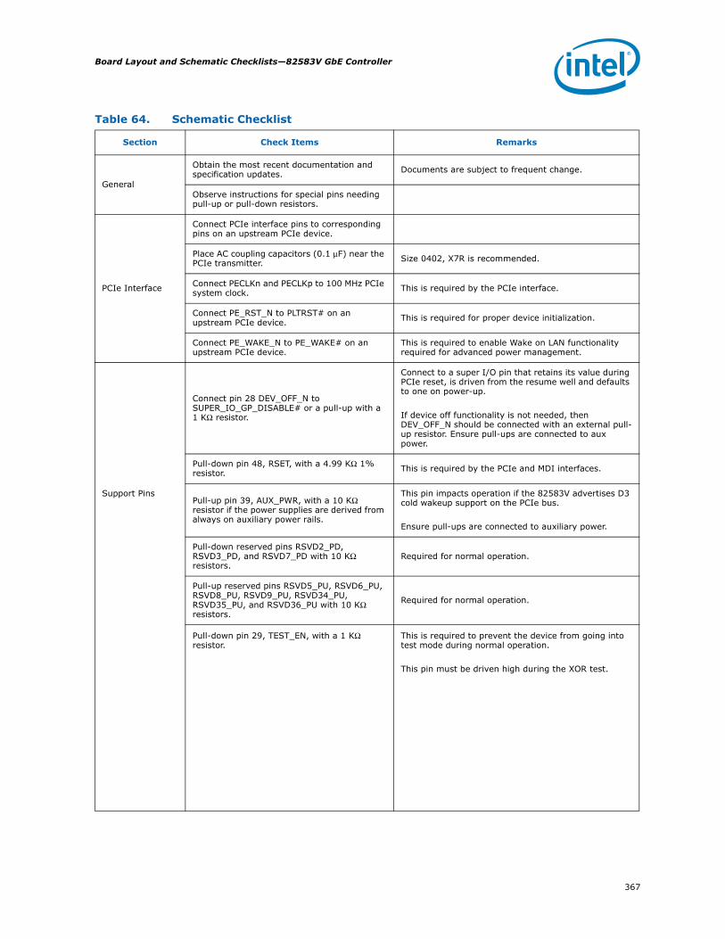
367
Board Layout and Schematic Checklists—82583V GbE Controller
Table 64. Schematic Checklist
Section Check Items Remarks
General
Obtain the most recent documentation and specification updates. Documents are subject to frequent change.
Observe instructions for special pins needing pull-up or pull-down resistors.
PCIe Interface
Connect PCIe interface pins to corresponding pins on an upstream PCIe device.
Place AC coupling capacitors (0.1 μF) near the PCIe transmitter. Size 0402, X7R is recommended.
Connect PECLKn and PECLKp to 100 MHz PCIe system clock. This is required by the PCIe interface.
Connect PE_RST_N to PLTRST# on an upstream PCIe device. This is required for proper device initialization.
Connect PE_WAKE_N to PE_WAKE# on an upstream PCIe device.
This is required to enable Wake on LAN functionality required for advanced power management.
Support Pins
Connect pin 28 DEV_OFF_N to SUPER_IO_GP_DISABLE# or a pull-up with a 1 KΩ resistor.
Connect to a super I/O pin that retains its value during PCIe reset, is driven from the resume well and defaults to one on power-up.
If device off functionality is not needed, then DEV_OFF_N should be connected with an external pull-up resistor. Ensure pull-ups are connected to aux power.
Pull-down pin 48, RSET, with a 4.99 KΩ 1% resistor. This is required by the PCIe and MDI interfaces.
Pull-up pin 39, AUX_PWR, with a 10 KΩ resistor if the power supplies are derived from always on auxiliary power rails.
This pin impacts operation if the 82583V advertises D3 cold wakeup support on the PCIe bus.
Ensure pull-ups are connected to auxiliary power.
Pull-down reserved pins RSVD2_PD, RSVD3_PD, and RSVD7_PD with 10 KΩ resistors.
Required for normal operation.
Pull-up reserved pins RSVD5_PU, RSVD6_PU, RSVD8_PU, RSVD9_PU, RSVD34_PU, RSVD35_PU, and RSVD36_PU with 10 KΩ resistors.
Required for normal operation.
Pull-down pin 29, TEST_EN, with a 1 KΩ resistor.
This is required to prevent the device from going into test mode during normal operation.
This pin must be driven high during the XOR test.
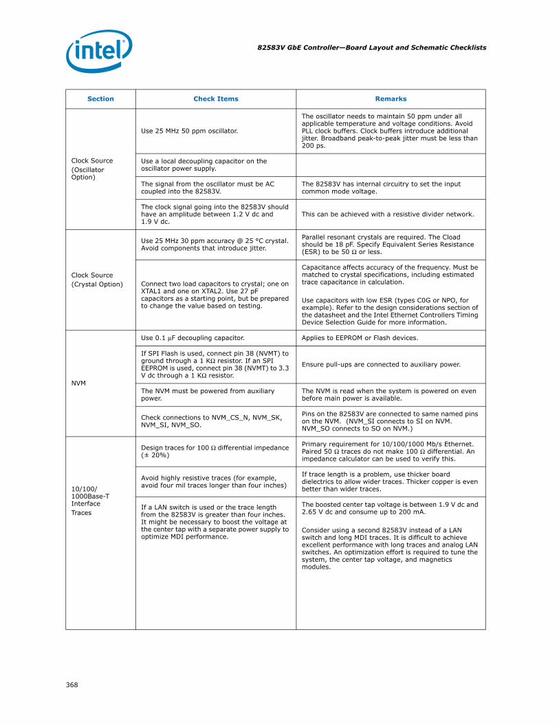
82583V GbE Controller—Board Layout and Schematic Checklists
368
Section Check Items Remarks
Clock Source(Oscillator Option)
Use 25 MHz 50 ppm oscillator.
The oscillator needs to maintain 50 ppm under all applicable temperature and voltage conditions. Avoid PLL clock buffers. Clock buffers introduce additional jitter. Broadband peak-to-peak jitter must be less than 200 ps.
Use a local decoupling capacitor on the oscillator power supply.
The signal from the oscillator must be AC coupled into the 82583V.
The 82583V has internal circuitry to set the input common mode voltage.
The clock signal going into the 82583V should have an amplitude between 1.2 V dc and 1.9 V dc.
This can be achieved with a resistive divider network.
Clock Source(Crystal Option)
Use 25 MHz 30 ppm accuracy @ 25 °C crystal. Avoid components that introduce jitter.
Parallel resonant crystals are required. The Cload should be 18 pF. Specify Equivalent Series Resistance (ESR) to be 50 Ω or less.
Connect two load capacitors to crystal; one on XTAL1 and one on XTAL2. Use 27 pF capacitors as a starting point, but be prepared to change the value based on testing.
Capacitance affects accuracy of the frequency. Must be matched to crystal specifications, including estimated trace capacitance in calculation.
Use capacitors with low ESR (types C0G or NPO, for example). Refer to the design considerations section of the datasheet and the Intel Ethernet Controllers Timing Device Selection Guide for more information.
NVM
Use 0.1 μF decoupling capacitor. Applies to EEPROM or Flash devices.
If SPI Flash is used, connect pin 38 (NVMT) to ground through a 1 KΩ resistor. If an SPI EEPROM is used, connect pin 38 (NVMT) to 3.3 V dc through a 1 KΩ resistor.
Ensure pull-ups are connected to auxiliary power.
The NVM must be powered from auxiliary power.
The NVM is read when the system is powered on even before main power is available.
Check connections to NVM_CS_N, NVM_SK, NVM_SI, NVM_SO.
Pins on the 82583V are connected to same named pins on the NVM. (NVM_SI connects to SI on NVM. NVM_SO connects to SO on NVM.)
10/100/1000Base-T InterfaceTraces
Design traces for 100 Ω differential impedance (± 20%)
Primary requirement for 10/100/1000 Mb/s Ethernet. Paired 50 Ω traces do not make 100 Ω differential. An impedance calculator can be used to verify this.
Avoid highly resistive traces (for example, avoid four mil traces longer than four inches)
If trace length is a problem, use thicker board dielectrics to allow wider traces. Thicker copper is even better than wider traces.
If a LAN switch is used or the trace length from the 82583V is greater than four inches. It might be necessary to boost the voltage at the center tap with a separate power supply to optimize MDI performance.
The boosted center tap voltage is between 1.9 V dc and 2.65 V dc and consume up to 200 mA.
Consider using a second 82583V instead of a LAN switch and long MDI traces. It is difficult to achieve excellent performance with long traces and analog LAN switches. An optimization effort is required to tune the system, the center tap voltage, and magnetics modules.

369
Board Layout and Schematic Checklists—82583V GbE Controller
Section Check Items Remarks
10/100/1000 Base-T InterfaceMagnetic Module(Integrated Option)
Qualify magnetic modules carefully for return loss, insertion loss, open circuit inductance, common mode rejection, and crosstalk isolation.
A magnetics module is critical to passing IEEE PHY conformance tests and EMI test.
Supply 1.9 V dc to the transformer center taps and use 0.01 μF bypass capacitors. If a LAN switch is used or the trace length from the 82583V is greater than four inches, it might be necessary to boost the voltage at the center tap with a separate external power supply to optimize MDI performance.
1.9 V dc at the center tap biases the 82583V's output buffers. Capacitors with low ESR should be used.
Ensure there are no termination resistors in the path between the 82583V and the magnetic module.
The 82583V has an internal termination network.
10/100/1000Base-T InterfaceMagnetics Module(Discrete Option withRJ-45 Connector)
Bob Smith termination: use 4 x 75 Ω resistors connected to each cable-side center tap.
Terminate pair-to-pair common mode impedance of the CAT5 cable.
Bob Smith termination: use an EFT capacitor attached to the chassis ground. Suggested values are 1500 pF/2 KV or 1000 pF/3 KV.
These capacitors provide high voltage isolation.
Supply 1.9 V dc to the system side transformer center taps and use 0.01 μF bypass capacitors. If a LAN switch is used or the trace length from the 82583V is greater than four inches. It might be necessary to boost the voltage at the center tap with a separate power supply to optimize MDI performance.
1.9 V dc at the center tap biases the 82583V's output buffers. Capacitors with low ESR should be used.
Ensure there is high voltage isolation to line side of the MDI traces and the Bob Smith termination.
The Bob Smith termination and the MDI traces should be >= 80 mils away from all components and traces on the same layer.
Do not use less than 10 mils of single ply woven epoxy (FR-4). There can be small air pockets between woven fibers. Use thicker, two ply, or three ply epoxy (FR-4).
Ensure there are no termination resistors in the path between the 82583V and the magnetics.
The 82583V has an internal termination network.
10/100/1000Base-T InterfaceChassis Ground
Provide a separate chassis ground to connect the shroud of the RJ-45 connector and to terminate the line side of the magnetic module.
This design improves EMI behavior.
Place pads for approximately 4-6 stitching capacitors to bridge the gap from chassis ground to signal ground.
Typical values range from 0.1 μF to 4.7 μF. The correct value should be determined experimentally to improve EMI. Past experiments have shown they are not required in some designs.

82583V GbE Controller—Board Layout and Schematic Checklists
370
Section Check Items Remarks
Integrated Power Supply(Option A and B)
Provide a 3.3 V dc supply. Use an auxiliary power supply.
Auxiliary power is necessary to support wake up from power down states.
Connect external PNP transistor's base to CTRL19 and the emitter to the 3.3 V dc supply. The collector supplies 1.9 V dc. The connections and transistor parameters are critical.
Connect external PNP transistor's base to CTRL10 and the emitter to the 3.3 V dc supply. The collector supplies 1.05 V dc. The connections and transistor parameters are critical. For option B only.
Connect a 5 KΩ resistor from CTRL19 to the 3.3 V dc supply.
Connect a 5 KΩ resistor from CTRL10 to the 3.3 V dc supply. For option B only.
For option A: Connect DIS_REG10 to ground.For option B: Connect DIS_REG10 to the 3.3 V dc supply.
Enable internal 1.05 V dc regulator if it is used.
Ensure that there is at least 10 μF of capacitance at the emitters of the PNPs.
The 3.3 V dc rail should have at least 25 μF of capacitance.
The 1.05 V dc and 1.9 V dc rails should have 20-40 μF of capacitance.
Place these to minimize the inductance from each power pin to the nearest decoupling capacitor.
Place decoupling and bulk capacitors close to 82583V, with some along every side, using short, wide traces and large vias. If power is distributed on traces, bulk capacitors should be used at both ends. If power is distributed on cards, bulk capacitors should be used at the connector.

371
Board Layout and Schematic Checklists—82583V GbE Controller
Section Check Items Remarks
External Power supply(Option C)
Derive all three power supplies from auxiliary power supplies.
Auxiliary power is necessary to support wake up from power down states.
If the 1.05 V dc and 1.9 V dc rails are externally supplied, ensure that CTRL10 and CTRL19 are tied to ground through a 3.3 KΩ resistor. Alternatively, they could be left floating.
Pull-down resistors do not need to be exactly 3.3 KΩ; however, they must be greater than 1 KΩ.
Connect DIS_REG10 to the 3.3 V dc supply with a 1 KΩ resister. Disable internal 1.05 V dc regulator.
It is recommended that the 1.9 V dc supply be tunable with a resistor option.
Tuning the 1.9 V dc supply might be required to optimize MDI performance.
The 3.3 V dc rail should have at least 25 μF of capacitance.
The 1.05 V dc and 1.9 V dc rails should have at least 20 μF of capacitance.
Place these to minimize the inductance from each power pin to the nearest decoupling capacitor.
Place decoupling and bulk capacitors close to 82583V, with some along every side, using short, wide traces and large vias. If power is distributed on traces, bulk capacitors should be used at both ends. If power is distributed on cards, bulk capacitors should be used at the connector.
All voltages should ramp to within their control bands in 100 ms or less. Voltages must ramp in sequence (3.3 V dc ramps first, 1.9 V dc ramps second, 1.05 V dc ramps last). The voltage rise must be monotonic. The minimum rise time on the 3.3 V dc power is 1 ms.
The 82583V has a power on reset circuit that requires a 1-100 ms ramp time. The rise must be montonic to so the power on reset triggers only once.
The sequence is required protect the ESD diodes connected to the power supplies from being forward biased
Integrated Power Supply(Option D)
Provide a 3.3 V dc and 1.9 V dc supply. Derive power supplies from auxiliary power supplies.
Auxiliary power is necessary to support wake up from power down states.
Ensure that CTRL10 and CTRL19 are tied to ground through a 3.3 KΩ resistor. Alternatively, they could be left floating.
Pull-down resistors do not need to be exactly 3.3 KΩ; however, they must be greater than 1 KΩ.
Connect DIS_REG10 to ground. Enable internal 1.05 V dc regulator.
The 3.3 V dc rail should have at least 25 μF of capacitance.
The 1.05 V dc and 1.9 V dc rails should have 20- 40 μF of capacitance.
Place these to minimize the inductance from each power pin to the nearest decoupling capacitor.
Place decoupling and bulk capacitors close to 82583V, with some along every side, using short, wide traces and large vias. If power is distributed on traces, bulk capacitors should be used at both ends. If power is distributed on cards, bulk capacitors should be used at the connector.

82583V GbE Controller—Board Layout and Schematic Checklists
372
Section Check Items Remarks
LED Circuits
Basic recommendation is a single green LED for activity and a dual (bi-color) LED for speed. Many other configurations are possible. LEDs are configurable through the NVM.
Two LED configurations are compatible with integrated magnetic modules. For the Link/Activity LED, connect the cathode to the LED1 pin and the anode to VCC. For the bi-color speed LED pair, have the LED2 signal drive one end. The other end should be connected to LED0. When LED2 is low, the orange LED is lit. When LED0 is low, the green LED is lit.
Connect LEDs to 3.3 V dc as indicated in reference schematics.
Use 3.3 V dc AUX for designs supporting wake-up. Consider adding one or two filtering capacitors per LED for extremely noisy situations. Suggested starting value is 470 pF.
Add current limiting resistors to LED paths.
Typical current limiting resistors are 250 Ω to 330 Ω when using a 3.3 V dc supply. Current limiting resistors are sometimes included with integrated magnetic modules.
Mfg Test The 82583V allows a JTAG Test Access Port to enable an XOR tree test.
Because of pin sharing the 82583V cannot be used in a JTAG chain. The JTAG pins must be individually driven and sampled.

373
Board Layout and Schematic Checklists—82583V GbE Controller
Note: This page intentionally left blank.

82583V GbE Controller—Models
374
15.0 Models
Contact your Intel Representative for access to the 82583V IBIS and HSPICE models.