intel 7 series family- intel management engine firmware 8 fw bring up guide 8.1.0.1248 pv.pdf2...
TRANSCRIPT

Intel® 7 Series Family- Intel® ME - 1.5MB FW Bring Up Guide
Intel® 7 Series Family- Intel® Management Engine Firmware 8.1
1.5MB Firmware Bring Up Guide
July 2012
Revision 8.1.0.1248 - PV Release
Intel Confidential

2 Intel® 7 Series Family - Intel® ME - 1.5MB FW Bring Up Guide
Intel Confidential
INFORMATION IN THIS DOCUMENT IS PROVIDED IN CONNECTION WITH INTEL PRODUCTS. NO LICENSE, EXPRESS OR IMPLIED, BY ESTOPPEL OR OTHERWISE, TO ANY INTELLECTUAL PROPERTY RIGHTS IS GRANTED BY THIS DOCUMENT. EXCEPT AS PROVIDED IN INTEL'S TERMS AND CONDITIONS OF SALE FOR SUCH PRODUCTS, INTEL ASSUMES NO LIABILITY WHATSOEVER AND INTEL DISCLAIMS ANY EXPRESS OR IMPLIED WARRANTY, RELATING TO SALE AND/OR USE OF INTEL PRODUCTS INCLUDING LIABILITY OR WARRANTIES RELATING TO FITNESS FOR A PARTICULAR PURPOSE, MERCHANTABILITY, OR INFRINGEMENT OF ANY PATENT, COPYRIGHT OR OTHER INTELLECTUAL PROPERTY RIGHT.
UNLESS OTHERWISE AGREED IN WRITING BY INTEL, THE INTEL PRODUCTS ARE NOT DESIGNED NOR INTENDED FOR ANY APPLICATION IN WHICH THE FAILURE OF THE INTEL PRODUCT COULD CREATE A SITUATION WHERE PERSONAL INJURY OR DEATH MAY OCCUR.
Intel may make changes to specifications and product descriptions at any time, without notice. Designers must not rely on the absence or characteristics of any features or instructions marked "reserved" or "undefined." Intel reserves these for future definition and shall have no responsibility whatsoever for conflicts or incompatibilities arising from future changes to them. The information here is subject to change without notice. Do not finalize a design with this information.
The products described in this document may contain design defects or errors known as errata which may cause the product to deviate from published specifications. Current characterized errata are available on request.
Contact your local Intel sales office or your distributor to obtain the latest specifications and before placing your product order.
All products, platforms, dates, and figures specified are preliminary based on current expectations, and are subject to change without notice. All dates specified are target dates, are provided for planning purposes only and are subject to change.
This document contains information on products in the design phase of development. Do not finalize a design with this information. Revised information will be published when the product is available. Verify with your local sales office that you have the latest datasheet before finalizing a design.
Intel® Active Management Technology requires activation and a system with a corporate network connection, an Intel® AMT-enabled chipset, network hardware and software. For notebooks, Intel® AMT may be unavailable or limited over a host OS-based VPN, when connecting wirelessly, on battery power, sleeping, hibernating or powered off. Results dependent upon hardware, setup & configuration. For more information, visit http://www.intel.com/technology/platform-technology/intel-amt.
No system can provide absolute security under all conditions. Requires an enabled chipset, BIOS, firmware and software, and a subscription with a capable Service Provider. Consult your system manufacturer and Service Provider for availability and functionality. Intel assumes no liability for lost or stolen data and/or systems or any other damages resulting thereof. For more information, visit http://www.intel.com/go/anti-theft.
KVM Remote Control (Keyboard, Video, Mouse) is only available with Intel®l Core™ i5 vPro and Core™ i7 vPro processors with Intel® Active Management technology activated and configured and with integrated graphics active. Discrete graphics are not supported.
Systems using Client Initiated Remote Access require wired LAN connectivity and may not be available in public hot spots or "click to accept" locations.
Warning: Altering clock frequency and/or voltage may (i) reduce system stability and useful life of the system and processor; (ii) cause the processor and other system components to fail; (iii) cause reductions in system performance; (iv) cause additional heat or other damage; and (v) affect system data integrity. Intel has not tested, and does not warranty, the operation of the processor beyond its specifications.
Code names featured are used internally within Intel to identify products that are in development and not yet publicly announced for release. Customers, licensees and other third parties are not authorized by Intel to use code names in advertising, promotion or marketing of any product or services and any such use of Intel's internal code names is at the sole risk of the user.
Intel, Intel® vPro™, and the Intel logo are trademarks of Intel Corporation in the U.S. and other countries.
*Other names and brands may be claimed as the property of others.
Copyright © 2012, Intel Corporation. All rights reserved.
Intel® 7 Series Family- Intel® ME - 1.5MB FW Bring Up Guide 3
Intel Confidential
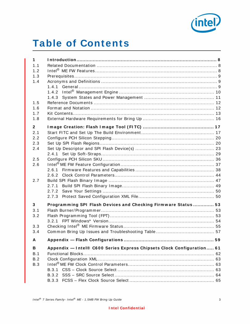
Table of Contents1 Introduction............................................................................................... 81.1 Related Documentation ................................................................................. 81.2 Intel® ME FW Features .................................................................................. 81.3 Prerequisites................................................................................................ 91.4 Acronyms and Definitions .............................................................................. 9
1.4.1 General ............................................................................................. 91.4.2 Intel® Management Engine ................................................................ 101.4.3 System States and Power Management ............................................... 11
1.5 Reference Documents ................................................................................. 121.6 Format and Notation ................................................................................... 121.7 Kit Contents............................................................................................... 131.8 External Hardware Requirements for Bring Up ................................................ 16
2 Image Creation: Flash Image Tool (FITC) ................................................ 172.1 Start FITC and Set Up The Build Environment................................................. 172.2 Configure PCH Silicon Stepping..................................................................... 202.3 Set Up SPI Flash Regions............................................................................. 202.4 Set Up Descriptor and SPI Flash Device(s) ..................................................... 23
2.4.1 Set Up Soft-Straps............................................................................ 292.5 Configure PCH Silicon SKU ........................................................................... 362.6 Intel®ME FW Feature Configuration............................................................... 37
2.6.1 Firmware Features and Capabilities ..................................................... 382.6.2 Clock Control Parameters................................................................... 44
2.7 Build SPI Flash Binary Image ....................................................................... 472.7.1 Build SPI Flash Binary Image.............................................................. 492.7.2 Save Your Settings ........................................................................... 502.7.3 Protect Saved Configuration XML File................................................... 50
3 Programming SPI Flash Devices and Checking Firmware Status .............. 533.1 Flash Burner/Programmer............................................................................ 533.2 Flash Programming Tool (FPT)...................................................................... 53
3.2.1 FPT Windows* Version....................................................................... 543.3 Checking Intel® ME Firmware Status............................................................. 553.4 Common Bring Up Issues and Troubleshooting Table ....................................... 57
A Appendix — Flash Configurations ............................................................. 59
B Appendix — Intel® C600 Series Express Chipsets Clock Configuration..... 61B.1 Functional Blocks........................................................................................ 62B.2 Clock Configuration XML .............................................................................. 63B.3 Intel®ME FW Clock Control Parameters.......................................................... 63
B.3.1 CSS – Clock Source Select ................................................................. 63B.3.2 SSS – SRC Source Select................................................................... 64B.3.3 FCSS – Flex Clock Source Select ......................................................... 65

Intel® 7 Series Family- Intel® ME - 1.5MB FW Bring Up Guide 4
Intel Confidential
B.3.4 PLLRCS – PLL Reference Clock Select .................................................. 69B.3.5 DPLLAC – Display PLL “A” Configuration............................................... 70B.3.6 DPLLBC – Display PLL “B” Configuration............................................... 70B.3.7 PLLEN – PLL Enable........................................................................... 70B.3.8 OCKEN – Output Clock Enable ............................................................ 70B.3.9 IBEN – Input Buffer Enable ................................................................ 72B.3.10 DIVEN – Divider Enable ..................................................................... 73B.3.11 PM1 – Power Management ................................................................. 74B.3.12 PM2 – Power Management ................................................................. 74B.3.13 SEBP1 – Single Ended Buffer Parameters ............................................. 75B.3.14 SEBP2 – Single Ended Buffer Parameters ............................................. 76B.3.15 SSCCTL – SSC Control....................................................................... 78B.3.16 PMSRCCLK1 – SRC Power Management ............................................... 79B.3.17 PMSRCCLK2 – SRC Power Management ............................................... 81B.3.18 PI12BiasParms – Phase Interpolators 1 & 2 Biasing Parameters .............. 83B.3.19 SSC2OCPARMS – SSC2 Overclock Parameters ...................................... 83B.3.20 PCH Clock output / ICC registers mapping - part A ................................ 83B.3.21 PCH Clock output / ICC registers mapping - part B ................................ 86

Intel® 7 Series Family- Intel® ME - 1.5MB FW Bring Up Guide 5
Intel Confidential
Figures2-1 Build | Environment Variables ...................................................................... 182-2 Build | Build Settings… ................................................................................ 192-3 PCH Silicon Stepping Combo Box .................................................................. 202-4 SKU Manager Combo Box ............................................................................ 372-5 Manageability Application Warning ................................................................ 412-6 Build | Build Image ..................................................................................... 502-7 Protecting FITC Configuration XML File .......................................................... 51A-1 Configuration “A” — Desktop/Server/Workstation or Mobile .............................. 59A-2 Configuration “B” — Mobile Only ................................................................... 59A-3 Configuration “C” — Desktop/Server/Workstation Only .................................... 60A-4 Configuration “D” — Mobile Only................................................................... 60B-1 Intel® 7 Series/C216 Chipset Family Full Clock Integration Mode Architecture..... 61
Tables1-1 Number Format Notation ............................................................................. 121-2 Data Format Notation.................................................................................. 121-3 Kit Contents............................................................................................... 132-1 Flash Image | PDR Region ........................................................................... 202-2 Flash Image | GbE Region............................................................................ 212-3 Flash Image | ME Region ............................................................................. 222-4 Flash Image | BIOS Region .......................................................................... 232-5 Flash Image | Descriptor Region ................................................................... 232-6 Flash Image | Descriptor Region | Descriptor Map ........................................... 242-7 Flash Image | Descriptor Region | Component Section..................................... 252-8 Flash Image | Descriptor Region | Master Access Section | CPU/BIOS ................ 262-9 Flash Image | Descriptor Region | Master Access Section | Manageability Engine (ME)
262-10 Flash Image | Descriptor Region | Master Access Section | GbE LAN.................. 272-11 Flash Image | Descriptor Region | VSCC Table | Add Table Entry....................... 272-12 Flash Image | Descriptor Region | VSCC Table | W25Q64BV (example).............. 282-13 Flash Image | Descriptor Region | OEM Section .............................................. 282-14 Flash Image | Descriptor Region | PCH Straps | PCH Strap 0 ............................ 292-15 Flash Image | Descriptor Region | PCH Straps | PCH Strap 2 ............................ 302-16 Flash Image | Descriptor Region | PCH Straps | PCH Strap 4 ............................ 302-17 Flash Image | Descriptor Region | PCH Straps | PCH Strap 7 ............................ 312-18 Flash Image | Descriptor Region | PCH Straps | PCH Strap 9 ............................ 322-19 Flash Image | Descriptor Region | PCH Straps | PCH Strap 10 .......................... 332-20 Flash Image | Descriptor Region | PCH Straps | PCH Strap 11 .......................... 342-21 Flash Image | Descriptor Region | PCH Straps | PCH Strap 15 .......................... 352-22 Flash Image | Descriptor Region | PCH Straps | PCH Strap 16 .......................... 362-23 Flash Image | Descriptor Region | PCH Straps | PCH Strap 17 .......................... 362-24 Flash Image | ME Region | Configuration | ME ................................................ 38

Intel® 7 Series Family- Intel® ME - 1.5MB FW Bring Up Guide 6
Intel Confidential
2-25 Flash Image | ME Region | Configuration | Power Packages .............................. 402-26 Flash Image | ME Region | Configuration | Features Supported ......................... 402-27 Flash Image | ME Region | Configuration | Intel® Anti-Theft Technology ............ 412-28 Flash Image | ME Region | Configuration | ME Debug Event Service .................. 422-29 ................................................................................................................ 432-30 Flash Image | ME Region | Configuration | ICC Data | ICC Profile 0 | FCIM/BTM Spe-
cific Registers............................................................................................. 442-31 Flash Image | ME Region | Configuration | ICC Data | ICC Profile 0 | ICC Registers .
452-32 Flash Image | ME Region | Configuration | ICC Data | ICC Profile 0 | Clock Range Def-
inition Record 0 .......................................................................................... 473-1 Common Bring Up Issues and Troubleshooting Table ....................................... 57B-1 SSC Blocks ................................................................................................ 62B-2 Clock Dividers ............................................................................................ 62B-3 Clock Source Select Parameters.................................................................... 64B-4 SRC Source Select Parameters ..................................................................... 65B-5 Flex Clock Source Select Parameters ............................................................. 66B-6 PLL Reference Clock Select Parameters.......................................................... 69B-7 PLL Enable Parameters ................................................................................ 70B-8 Output Clock Enable Parameters................................................................... 71B-9 Input Buffer Enable Parameters .................................................................... 72B-10 Divider Enable Parameters ........................................................................... 73B-11 Power Management Parameters.................................................................... 74B-12 Power Management Parameters.................................................................... 75B-13 Single Ended Buffer Parameters.................................................................... 75B-14 Single Ended Buffer Parameters.................................................................... 77B-15 SSC Control Parameters .............................................................................. 78B-16 SRC Power Management.............................................................................. 80B-17 SRC Power Management.............................................................................. 82B-18 Phase Interpolators 1 & 2 Biasing Parameters................................................. 83B-19 SSC2 Overclock Parameters ......................................................................... 83B-20 PCH Clock output / ICC registers mapping - part A .......................................... 84B-21 PCH Clock output / ICC registers mapping - part B .......................................... 87

Intel® 7 Series Family- Intel® ME - 1.5MB FW Bring Up Guide 7
Intel Confidential
Revision History
§ §
Revision Description Date
8.1.0.1237 Beta Release: See change bars on the left side of the page March 2012
8.1.0.1248 PC Release: See change bars on the left side of the page June 2012
8.1.0.1248 PV Release: See change bars on the left side of the page July 2012

Intel® 7 Series Family - Intel® ME - 1.5MB FW Bring Up Guide 8
Intel Confidential
Introduction
1 Introduction
This document covers the Intel® Management Engine Firmware (Intel® ME) 8.1 - 1.5MB SKU Firmware bring up procedure. Intel® ME is tied to essential platform functionality — this dependency cannot be avoided for engineering reasons.
The bring up procedure primarily involves building a Serial Peripheral Interface (SPI) Flash image that will contain:
• [required] Descriptor region — Contains sizing information for all other SPI Flash image regions, SPI settings (including Vendor Specific Configuration - or VSCC - tables, SPI device parameters), and region access permissions.
• [required] BIOS region — Contains firmware for the processor (or host) and/or Embedded Controller (EC).
• [required] Intel® ME FW region — Contains firmware for the Intel® Management Engine.
• [optional] GbE region — Contains firmware for Intel® LAN solution.
For more details on SPI Flash layout, see the document Intel® 7 Series/C216 Chipset Family SPI Flash Programming Guide and Appendix A. Once the SPI Flash image is built, it will be programmed to the target Intel® 7 Series/C216 Chipset Family based platform and the platform will be booted. This document also covers any tests and checks required to ensure that this boot process is successful and that Intel® ME 1.5MB FW is operating as expected.
1.1 Related DocumentationVIP: Kit# 474804 - Intel® Ethernet Network Connections (16.3 PC OEM Gen) - LAN Software Drivers -- 05-May-2011 LAN Acess Division (LAD) - V16.3C00061 TIC = 239717 .Release 16.3 Production Candidate with selected bug fixes for E1K, E1C and IXE silicon products.
1.2 Intel® ME FW FeaturesThis firmware release includes the following applications:
• Platform Clocks – Tune Intel® 7 Series/C216 Chipset Family clock silicon to the parameters of a specific board, configure clocks at run time, and power management clocks. Benefit: Allows extensive customizability and soft control of “Third generation” clock solution and makes clocks available before CPU powers up.
• Silicon Workaround Capability – Intel® ME FW will have limited capabilities to perform targeted workarounds for silicon issues. Benefit: Allows Intel® ME FW to address some issues that otherwise would require a new silicon stepping.
• Thermal Reporting – Intel® ME FW has the ability to collect platform thermal data and provide that data to embedded controllers and super I/O devices over SMLINK1 as well as in memory map I/O space.

Intel® 7 Series Family - Intel® ME - 1.5MB FW Bring Up Guide 9
Intel Confidential
Introduction
1.3 PrerequisitesBefore this document is read and utilized, it is essential that the reader first review the 1.5MB FW Release Notes (included with this Intel® ME 1.5MB FW kit).
This document is constructed so that the reader can complete the bring up steps as given for the Intel Customer Reference Board (CRB). However, in the case that bring up is being performed on a different Intel® 7 Series Family based platform, this document will highlight any changes that must be imposed onto the bring up steps accordingly.
This document makes only the following limited assumptions regarding hardware:
• The platform is Intel® 7 Series Family based
• The platform is equipped with one or more SPI Flash devices with a total capacity sufficient for storing all relevant firmware images.
1.4 Acronyms and Definitions
1.4.1 General
Acronym or Term Definition
API Application Programming Interface
ASCII American Standard Code for Information Interchange
BIOS Basic Input Output System
CPU Central Processing Unit
DIMM Dual In-line Memory Module
DLL Dynamic Link Library
DMI Direct Media Interface
EC Embedded Controller
EEPROM Electrically Erasable Programmable Read Only Memory
FDI Flexible Display Interface
FW Firmware
GbE Gigabit Ethernet
HECI Host Embedded Controller Interface (aka Intel® MEI)
IBV Independent BIOS Vendor
ID Identification
Intel® ME Intel® Management Engine (Intel®ME)
Intel® MEI Intel® Management Engine Interface (Intel® MEI) (renamed from HECI)
Intel® IPT Intel® Identity Protection Technology (Intel® IPT)
IMSS Intel® Management and Security Status Application
ISV Independent Software Vendor
JTAG Joint Test Action Group
KVM Keyboard, Video, Mouse
LAN Local Area Network
LED Light Emitting Diode
NVM Non-Volatile Memory
Intel® 7 Series Family - Intel® ME - 1.5MB FW Bring Up Guide 10
Intel Confidential
Introduction
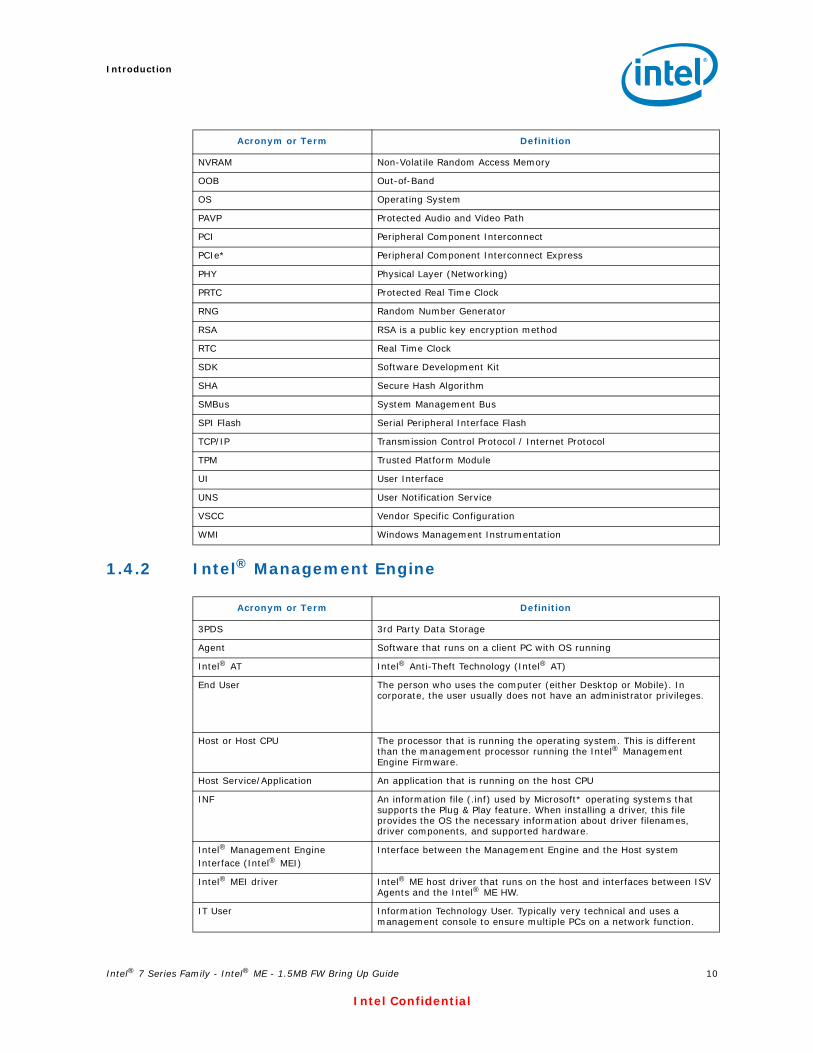
1.4.2 Intel® Management Engine
NVRAM Non-Volatile Random Access Memory
OOB Out-of-Band
OS Operating System
PAVP Protected Audio and Video Path
PCI Peripheral Component Interconnect
PCIe* Peripheral Component Interconnect Express
PHY Physical Layer (Networking)
PRTC Protected Real Time Clock
RNG Random Number Generator
RSA RSA is a public key encryption method
RTC Real Time Clock
SDK Software Development Kit
SHA Secure Hash Algorithm
SMBus System Management Bus
SPI Flash Serial Peripheral Interface Flash
TCP/IP Transmission Control Protocol / Internet Protocol
TPM Trusted Platform Module
UI User Interface
UNS User Notification Service
VSCC Vendor Specific Configuration
WMI Windows Management Instrumentation
Acronym or Term Definition
3PDS 3rd Party Data Storage
Agent Software that runs on a client PC with OS running
Intel® AT Intel® Anti-Theft Technology (Intel® AT)
End User The person who uses the computer (either Desktop or Mobile). In corporate, the user usually does not have an administrator privileges.
Host or Host CPU The processor that is running the operating system. This is different than the management processor running the Intel® Management Engine Firmware.
Host Service/Application An application that is running on the host CPU
INF An information file (.inf) used by Microsoft* operating systems that supports the Plug & Play feature. When installing a driver, this file provides the OS the necessary information about driver filenames, driver components, and supported hardware.
Intel® Management EngineInterface (Intel® MEI)
Interface between the Management Engine and the Host system
Intel® MEI driver Intel® ME host driver that runs on the host and interfaces between ISV Agents and the Intel® ME HW.
IT User Information Technology User. Typically very technical and uses a management console to ensure multiple PCs on a network function.
Acronym or Term Definition

Intel® 7 Series Family - Intel® ME - 1.5MB FW Bring Up Guide 11
Intel Confidential
Introduction
1.4.3 System States and Power Management
LMS Local Management Service: A SW application which runs on the host machine and provide a secured communication between the ISV agent and the Intel® Management Engine Firmware.
Intel® ME Intel® Management Engine: The embedded processor residing in the chipset PCH
MECI ME-VE Communication Interface
NVM Non-Volatile Memory: A type of memory that will retain its contents even if power is removed.
OOB Interface Out Of Band interface: This is SOAP/XML interface over secure or non-secure TCP protocol.
OS not Functional The Host OS is considered non-functional in Sx power state and any one of the following cases when system is in S0 power state:• OS is hung• After PCI reset• OS watch dog expires• OS is not present
System States Operating System power states such as S0. See detailed definitions in System States and Power Management section.
UIM User Identifiable Mark
Acronym or Term Definition
G3 A system state of Mechanical Off where all power is disconnected from the system. G3 power state does not necessarily indicate that RTC power is removed.
M0 Intel® Management Engine power state where all HW power planes are activated. The host power state is S0.
M3 Intel® Management Engine power state where all HW power planes are activated however the host power state is different than S0 (Some host power planes are not activated). Host PCIe* interface are unavailable to the host software. Main memory is not available for Intel® Management Engine use.
M-Off No power is applied to the management processor subsystem. Intel® Management Engine is not operating.
OS Hibernate System state where the OS state is saved on the hard drive.
S0 A system state where power is applied to all HW devices and the system is running normally.
S1, S2, S3 A system state where the host CPU is halted but power remains available to the memory system (memory is in self-refresh mode).
S4 A system state where the host CPU and memory are not active.
S5 A system state where all power to the host system is off, however the power cord (and/or battery in mobile designs) is still connected.
Shut Down Equivalent to the S5 state.
Snooze Mode Intel® Management Engine activities are mostly suspended to save power. The Intel® Management Engine monitors HW activities and can restore its activities depending on the HW event.
Standby System state where the OS state is saved in memory and resumed from the memory when mouse/keyboard is clicked.
Sx All S states which are different than S0.
Acronym or Term Definition

Intel® 7 Series Family - Intel® ME - 1.5MB FW Bring Up Guide 12
Intel Confidential
Introduction
1.5 Reference Documents
Note: * Unless specified otherwise, a document can be ordered by providing its reference number to your Intel Field Applications Engineer.
1.6 Format and NotationThe formats and notations used within this document model are those typically used by BIOS vendors. This section describes the formatting and the notations that will be followed in this document.
Document Doc Number/Location*
Maho Bay and Carlow-WS – Platform Design Guide 473718 / IBL
Chief River Mobile CRB– Platform Design Guide 29635 / IBL
Intel® Management Engine (Intel® ME) and Embedded Controller Interaction for Chief River Platform
471984 / IBL
RS – Intel® Management Engine BIOS Writers Guide 31007 / *
[Maho Bay / Chief River / Carlow] Platforms - Intel® Management Engine (Intel® ME) 8.0 - 1.5 MB SKU Firmware for Intel® 7 Series Family - Compliancy and Testing Guide -Rev. 0.8
464265 / IBL
Intel® 82576 and 82579 Gigabit Ethernet Controllers – Intel Software Support for Cisco’s MACsec Protocol Supplicant – 10-Dec-2010
461067 / IBL
Table 1-1. Number Format Notation
Number Format Notation Example
Decimal (default) d 14d. Note that any number without an explicit suffix can be assumed to be decimal.
Binary b 1110b
Hex h 0Eh
Hex 0x 0x0E
Table 1-2. Data Format Notation
Data Type Notation Size
Bit b Smallest unit, 0 or 1
Byte B 8 bits
Word W 16 bits or 2 bytes
Double-word DW 32 bits or 4 bytes
Quad-word QW 8 bytes or 4 words
Kilobyte KB 1024 bytes
Megabit Mb 1,048,576 bits or 128 KB
Megabyte MB 1,048,576 bytes or 1024 KB
Gigabit Gb 1,073,741,824 bits
Gigabyte GB 1024 MB

Intel® 7 Series Family - Intel® ME - 1.5MB FW Bring Up Guide 13
Intel Confidential
Introduction
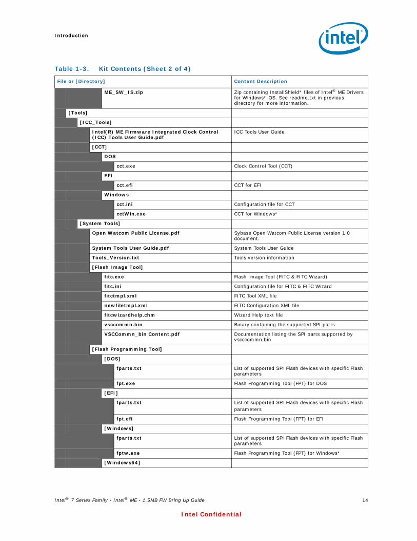
1.7 Kit ContentsThe Intel® ME 1.5MB FW kit can be downloaded from VIP (https://platformsw.intel.com/). The contents of this kit are detailed below (Note that only key files are listed).
Table 1-3. Kit Contents (Sheet 1 of 4)
File or [Directory] Content Description
[root] Root directory
1.5MB FW Bring Up Guide.pdf This document
1.5MB FW Getting Started Guide.pdf 1.5MB FW Getting started guide.
SPI programming guide.pdf How to program SPI device parameters, VSCC tables, descriptor region details. Also contains a complete SPI Flash softstrap reference.
[Image Components]
[BIOS]
IVB091.rom BIOS image only for Intel® CRB. This BIOS image works for both desktop and mobile CRBs.For other Intel® 7 Series Family based platforms, a custom BIOS image will be required.
[GbE]
82579_NVM_4_DESKTOP.bin Intel® LAN PHY firmware image, supports PHY A2 and B0 only. This image is recommended for testing power flows with connectivity. This image is for desktop platforms only.
82579_NVM_3_MOBILE.bin Intel® LAN PHY firmware image, supports PHY A2 and B0 only. This image is recommended for testing power flows with connectivity. This image is for mobile platforms only.
[ME]
ME8_1.5M_PreProduction.BIN Intel® ME firmware image (Non Production FW) - supports unfused Intel® 7 Series Family PCH steppings:• Unfused PPT ES0 (B0 Super SKU)
Note: For PAVP Testing, you must match Production FW with Production Part and Non Production FW with Non Production Parts.
ME8_1.5M_Production.BIN Intel® ME firmware image (Production FW) - supports fused and unfused Intel® 7 Series Family PCH steppings:• Unfused PPT ES0 (B0 Super SKU)• Fused PPT Pre-QS and QS
Note: For PAVP Testing, you must match Production FW with Production Part and Non Production FW with Non Production Parts.
[Installers]
Intel® ME SW Installation Guide.pdf Intel®ME SW Installation Guide
[ME_SW]
Setup.exe Install executable (non-InstallShield) of Intel® ME Drivers for Windows* OS. See readme.txt for more information.
[ME_SW_IS]
Intel® 7 Series Family - Intel® ME - 1.5MB FW Bring Up Guide 14
Intel Confidential
Introduction
ME_SW_IS.zip Zip containing InstallShield* files of Intel® ME Drivers for Windows* OS. See readme.txt in previous directory for more information.
[Tools]
[ICC_Tools]
Intel(R) ME Firmware Integrated Clock Control (ICC) Tools User Guide.pdf
ICC Tools User Guide
[CCT]
DOS
cct.exe Clock Control Tool (CCT)
EFI
cct.efi CCT for EFI
Windows
cct.ini Configuration file for CCT
cctWin.exe CCT for Windows*
[System Tools]
Open Watcom Public License.pdf Sybase Open Watcom Public License version 1.0 document.
System Tools User Guide.pdf System Tools User Guide
Tools_Version.txt Tools version information
[Flash Image Tool]
fitc.exe Flash Image Tool (FITC & FITC Wizard)
fitc.ini Configuration file for FITC & FITC Wizard
fitctmpl.xml FITC Tool XML file
newfiletmpl.xml FITC Configuration XML file
fitcwizardhelp.chm Wizard Help text file
vsccommn.bin Binary containing the supported SPI parts
VSCCommn_bin Content.pdf Documentation listing the SPI parts supported by vscccommn.bin
[Flash Programming Tool]
[DOS]
fparts.txt List of supported SPI Flash devices with specific Flash parameters
fpt.exe Flash Programming Tool (FPT) for DOS
[EFI]
fparts.txt List of supported SPI Flash devices with specific Flashparameters
fpt.efi Flash Programming Tool (FPT) for EFI
[Windows]
fparts.txt List of supported SPI Flash devices with specific Flash parameters
fptw.exe Flash Programming Tool (FPT) for Windows*
[Windows64]
Table 1-3. Kit Contents (Sheet 2 of 4)
File or [Directory] Content Description

Intel® 7 Series Family - Intel® ME - 1.5MB FW Bring Up Guide 15
Intel Confidential
Introduction
fparts.txt List of supported SPI Flash devices with specific Flash parameters
fptw64.exe Flash Programming Tool (FPT) for Windows* (64-bit) OS
[FWUpdate]
[EFI]
FWUpdLcl.efi FW Update Tool (EFI version)
[Local-DOS]
FWUpdLcl.exe FW Update Tool (DOS version)
[Local-Win]
FWUpdLcl.exe FW Update Tool (Windows* version 32bit)
[Local-Win64]
FWUpdLcl64.exe FW Update Tool (Windows* version 64bit)
[MEInfo]
[DOS]
MEInfo.exe Intel®ME Information Tool (DOS version)
[EFI]
MEInfo.efi Intel®ME Information Tool (EFI version)
[Windows]
MEInfoWin.exe Intel®ME Information Tool (Windows* version 32bit)
[Windows64]
MEInfoWin64.exe Intel®ME Information Tool (Windows* version 64bit)
[MEManuf]
[DOS]
MEManuf.cfg Intel®ME Manufacturing Tool config file
MEManuf.exe Intel®ME Manufacturing Tool (DOS version)
vsccommn.bin Binary containing the supported SPI parts
VSCCommn_bin Content.pdf Documentation listing the SPI parts supported by vscccommn.bin
[EFI]
MEManuf.cfg Intel®ME Manufacturing Tool config file
MEManuf.efi Intel®ME Manufacturing Tool (EFI version)
vsccommn.bin Binary containing the supported SPI parts
[Windows]
MEManuf.cfg Intel®ME Manufacturing Tool config file
MEManufWin.exe Intel®ME Manufacturing Tool (Windows* version 32bit)
vsccommn.bin Binary containing the supported SPI parts
VSCCommn_bin Content.pdf Documentation listing the SPI parts supported by vscccommn.bin
[Windows64]
Table 1-3. Kit Contents (Sheet 3 of 4)
File or [Directory] Content Description
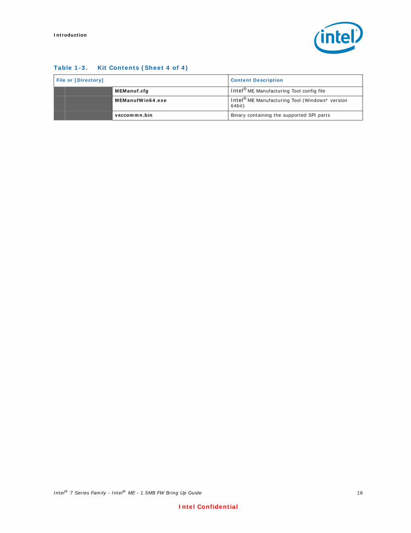
Intel® 7 Series Family - Intel® ME - 1.5MB FW Bring Up Guide 16
Intel Confidential
Introduction
MEManuf.cfg Intel®ME Manufacturing Tool config file
MEManufWin64.exe Intel®ME Manufacturing Tool (Windows* version 64bit)
vsccommn.bin Binary containing the supported SPI parts
Table 1-3. Kit Contents (Sheet 4 of 4)
File or [Directory] Content Description
Intel® 7 Series Family - Intel® ME - 1.5MB FW Bring Up Guide 17
Intel Confidential
Introduction
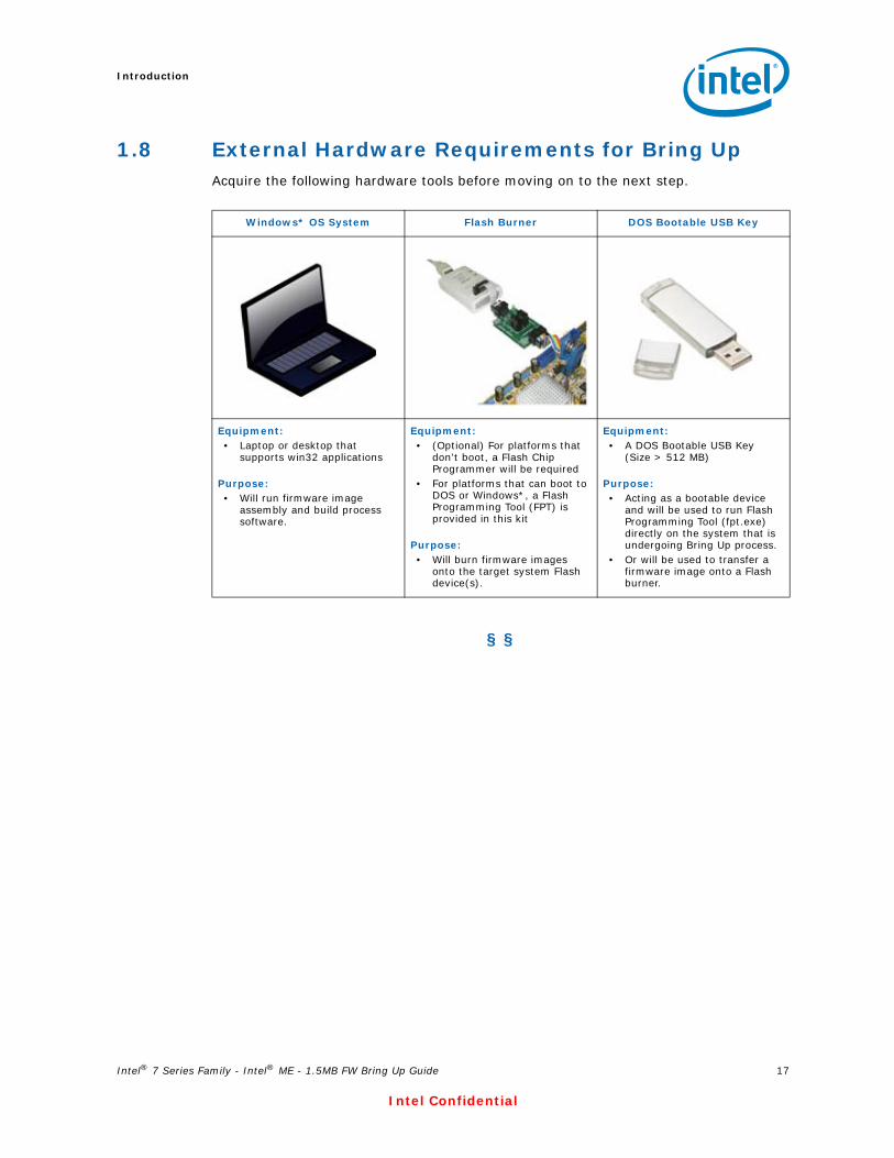
1.8 External Hardware Requirements for Bring UpAcquire the following hardware tools before moving on to the next step.
§ §
Windows* OS System Flash Burner DOS Bootable USB Key
Equipment:• Laptop or desktop that
supports win32 applications
Purpose: • Will run firmware image
assembly and build process software.
Equipment:• (Optional) For platforms that
don’t boot, a Flash Chip Programmer will be required
• For platforms that can boot to DOS or Windows*, a Flash Programming Tool (FPT) is provided in this kit
Purpose: • Will burn firmware images
onto the target system Flash device(s).
Equipment:• A DOS Bootable USB Key
(Size > 512 MB)
Purpose: • Acting as a bootable device
and will be used to run Flash Programming Tool (fpt.exe) directly on the system that is undergoing Bring Up process.
• Or will be used to transfer a firmware image onto a Flash burner.

Intel® 7 Series Family- Intel® ME - 1.5MB FW Bring Up Guide 17
Intel Confidential
Image Creation: Flash Image Tool (FITC)
2 Image Creation: Flash Image Tool (FITC)
Flash Image Tool (FITC) will be used to generate a full SPI Flash binary image with Descriptor, GbE, BIOS, and Intel® ME Regions. Use the steps shown in following sections.
Note: The FITC Tool may be updated throughout the release cycles. As a general rule, please ensure you use the tools, images and other content from the same kit and refrain from using different version tools.
After this SPI Flash image is created, it will need to be burned onto the target platform’s SPI Flash device(s). Section 3, “Programming SPI Flash Devices and Checking Firmware Status” later in this document provides steps to do this.
2.1 Start FITC and Set Up The Build Environment1. Invoke Flash Image Tool. Using Explorer*, navigate to [root]\Tools\System
Tools\Flash Image Tool. Ensure that FITC's directory contents are intact (see Section 1.7). Double-click fitc.exe.
2. In the main menu select Build | Environment Variables…. Edit your configuration as shown below. Note that in the example, [root]\Tools\System Tools\Flash Image Tool is “.”.
— Keep the Working Directory $WorkingDir as “.”— Source Directory $SourceDir is where FITC will look to find binary images
during the image creation process, change $SourceDir to “.\..\..\..\Image Components”
— Destination Directory $DestDir is where FITC will save the SPI Flash binary image, keep $DestDir as “.”

Intel® 7 Series Family- Intel® ME - 1.5MB FW Bring Up Guide 18
Intel Confidential
Image Creation: Flash Image Tool (FITC)
3. Click OK to apply your changes.
Figure 2-1. Build | Environment Variables

Intel® 7 Series Family- Intel® ME - 1.5MB FW Bring Up Guide 19
Intel Confidential
Image Creation: Flash Image Tool (FITC)
4. In the main menu select Build | Build Settings…. Leave the defaults for Output path, Generate intermediate build files, and Build compact image as shown. Change the Flash Block/Sector Erase Size as appropriate for your SPI flash part(s). Click OK to apply your changes.
5. In the main menu select File | Open…. In the Open dialog that appears navigate to [root]\Tools\System Tools\Flash Image Tool. Click on newfiletmpl.xml and click OK.
Figure 2-2. Build | Build Settings…

Intel® 7 Series Family- Intel® ME - 1.5MB FW Bring Up Guide 20
Intel Confidential
Image Creation: Flash Image Tool (FITC)
2.2 Configure PCH Silicon SteppingLeave the PCH Silicon Stepping Combo Box at its default value of Intel® 7 Series Chipset.
2.3 Set Up SPI Flash Regions
Figure 2-3. PCH Silicon Stepping Combo Box
Table 2-1. Flash Image | PDR Region
Location Parameter CRB Set To Settings for Any Platform
Follow navigation tree below:• Select the Flash Image• Select Flash Image | PDR
Region• Set the parameters in the
PDR Region section as shown
PDR Region Length PDR Region is enabled
Displays Region size information when Binary input file is specified.
Binary Input File PDR Region is enabled
Load a Platform Data Region binary if required and available.
...or if NOT using Platform Data Region (PDR)
A red “X” will indicate whether this Region is disabled. If this Region is not disabled, disable it by right-clicking on Flash Image | PDR Region and selecting Disable Region.

Intel® 7 Series Family- Intel® ME - 1.5MB FW Bring Up Guide 21
Intel Confidential
Image Creation: Flash Image Tool (FITC)
Table 2-2. Flash Image | GbE Region
Location Parameter CRB Set To Settings for Any Platform
Follow navigation tree below:• Select the Flash Image• Select Flash Image | GbE
Region• Set the parameters in the
GbE Region section as shown
Yellow means custom settings may be required.
GbE LAN region length
0x00000000
Binary input file Navigate to your Source Directory (as specified inSection 2.1) and switch to the GbE subdirectory. Choose the appropriate Intel®GbE LAN Firmware binary image.
If not using Intel®LAN then leave this parameter blank.
Intel® Integrated LAN Enable
true This field only is editable after an Intel® integrated LAN image is loaded. If not planning to validate Intel® LAN on target platform, or for debug reasons, set to false.
Major Version 0 Displays major revision value for Intel® LAN GbE FW version when Binary input file is specified.
Minor Version 0 Displays minor revision value for Intel® LAN GbE FW version when Binary input file is specified.
Image ID 0 Displays image ID value for Intel® LAN GbE FW version when Binary input file is specified.
...or if not using Intel®wired LAN device
A red “X” will indicate whether this Region is disabled. If this Region is not disabled, disable it by right-clicking on Flash Image | GbE Region and selecting Disable Region.
Intel® 7 Series Family- Intel® ME - 1.5MB FW Bring Up Guide 22
Intel Confidential
Image Creation: Flash Image Tool (FITC)
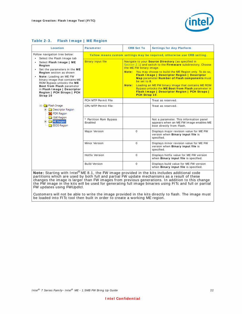
Table 2-3. Flash Image | ME Region
Location Parameter CRB Set To Settings for Any Platform
Follow navigation tree below:• Select the Flash Image tab• Select Flash Image | ME
Region• Set the parameters in the ME
Region section as shown • Note: Loading an ME FW
binary image that contains ME ROM Bypass unlocks the ME Boot from Flash parameter in Flash Image | Descriptor Region | PCH Straps | PCH Strap 10
Yellow means custom settings may be required, otherwise use CRB setting.
Binary input file Navigate to your Source Directory (as specified in Section 2.1) and switch to the Firmware subdirectory. Choose the ME FW binary image.Note: You may choose to build the ME Region only. To do so,
Flash Image | Descriptor Region | Descriptor Map parameter Number of Flash components must be set to 0.
Note: Loading an ME FW binary image that contains ME ROM Bypass unlocks the ME Boot from Flash parameter in Flash Image | Descriptor Region | PCH Straps | PCH Strap 10.
PCH MTP Permit File Treat as reserved.
CPU MTP Permit File Treat as reserved.
* Partition Rom Bypass Enabled
Not a parameter. This information panel appears when an ME FW image enables ME boot directly from Flash.
Major Version 0 Displays major revision value for ME FW version when Binary input file is specified.
Minor Version 0 Displays minor revision value for ME FW version when Binary input file is specified.
Hotfix Version 0 Displays hotfix value for ME FW version when Binary input file is specified.
Build Version 0 Displays build value for ME FW version when Binary input file is specified.
Note: Starting with Intel®ME 8.1, the FW image provided in the kits includes additional code partitions which are used by both full and partial FW update mechanisms as a result of these changes the image is larger than FW images from previous generations. In addition to this change the FW image in the kits will be used for generating full image binaries using FITc and full or partial FW updates using FWUpdlcl.
Customers will not be able to write the image provided in the kits directly to flash. The image must be loaded into FITc tool then built in order to create a working ME region.

Intel® 7 Series Family- Intel® ME - 1.5MB FW Bring Up Guide 23
Intel Confidential
Image Creation: Flash Image Tool (FITC)
2.4 Set Up Descriptor and SPI Flash Device(s)
Table 2-4. Flash Image | BIOS Region
Location Parameter CRB Set To Settings for Any Platform
Follow navigation tree below:• Select the Flash Image tab• Select Flash Image | BIOS
Region• Set the parameters in the
BIOS Region section as shown
Yellow means custom settings may be required, otherwise use CRB setting.
BIOS region length 0x00000000 This field allows user to allocate a specific size in the SPI Flash for the BIOS image. If set to 0, FITC will automatically set the size based on the BIOS image.
Binary input file For the Intel® CRB navigate to your
Source Directory (as specified in
Section 2.1) and switch to the BIOS
subdirectory. Choose the BIOS binary image.
For all other platforms point this parameter to the appropriate BIOS image.If BIOS is stored in a separate SPI Flash device or in FWH (see Configurations “B”, “C”, and “D” in Appendix A) then leave this parameter blank.
Table 2-5. Flash Image | Descriptor Region
Location Parameter CRB Set To Settings for Any Platform
Follow navigation tree below:• Select the Flash Image tab.
Select Flash Image | Descriptor Region
• Set the parameters in the Descriptor Region section as shown
Yellow means custom settings may be required, otherwise use CRB setting.
Descriptor region length 0x00000000 Leave this at zero. Allows FITC to auto-size the descriptor region length.

Intel® 7 Series Family- Intel® ME - 1.5MB FW Bring Up Guide 24
Intel Confidential
Image Creation: Flash Image Tool (FITC)
Table 2-6. Flash Image | Descriptor Region | Descriptor Map
Location Parameter CRB Set To Settings for Any Platform
Follow navigation tree below:• Select the Flash Image tab• Select Flash Image |
Descriptor Region | Descriptor Map
• Set the parameters in the Descriptor Map section as shown
Yellow means custom settings may be required, otherwise use CRB setting.
Region base address 0x04 Read Only, See SPI programming Guide for details.
Number of Flash components
2 Number of SPI Flash devices on the platform 1 or 2 = Total SPI Flash devices 0 = Build ME region only
Component base address 0x03 Read Only, See SPI programming Guide for details.
Number of PCH straps 18 Read Only, See SPI programming Guide for details.
PCH straps base address 0x10 Read Only, See SPI programming Guide for details.
Number of Masters 2 Read Only, See SPI programming Guide for details.
Master base address 0x06 Read Only, See SPI programming Guide for details.
Number of PROC straps 1 Read Only, See SPI programming Guide for details.
PROC straps base address 0x20 Read Only, See SPI programming Guide for details.

Intel® 7 Series Family- Intel® ME - 1.5MB FW Bring Up Guide 25
Intel Confidential
Image Creation: Flash Image Tool (FITC)
Table 2-7. Flash Image | Descriptor Region | Component Section
Location Parameter CRB Set To Settings for Any Platform
Follow navigation tree below:• Select the Flash Image tab.
Select Flash Image | Descriptor Region | Component Section
• Set the parameters in the Component Section section as shown
Yellow means custom settings may be required, otherwise use CRB setting.
Read ID and Read Status clock frequency
33MHz Lowest common frequency of all SPI Flash parts on the platform.
Write and erase clock frequency
33MHz Lowest common frequency of all SPI Flash parts on the platform.
Fast read clock frequency 33MHz In order for PCH HW to override its own internal default value (20 MHz), Fast read support must be set To true.
Fast read support true true = Enables opcode 0Bh opcode on a read. This allows for faster read frequencies on serial flash by having a single dummy byte before valid data is output from the flash.
Read clock frequency 20MHz
Flash component 2 density
8MB Size of second SPI Flash part on the platform.Note: This value will be grayed out if the number of SPI Flash components is set to 1 in the Descriptor Map options.
Flash component 1 density
8MB Size of first SPI Flash part on the platform.
Dual Output Fast Read Support
false This field enables the opcode 3Bh to use Single Input Dual Output Fast Read. This speeds up the fast read throughput of the serial flash part.
Note: This should only be set to ‘true’ if all Serial Flash parts support the 3Bh command. See Intel® 7 Series Chipset SPI programming Guide for more details.
Invalid instruction 3 0 Opcode entered here will not be allowed by the PCH’s SPI controller for HW sequencing. See Intel® 7 Series Chipset SPI programming Guide for more details.0 = no instruction is specified
Invalid instruction 2 0 Opcode entered here will not be allowed by the PCH’s SPI controller for HW sequencing. See Intel® 7 Series Chipset SPI programming Guide for more details.0 = no instruction is specified
Invalid instruction 1 0 Opcode entered here will not be allowed by the PCH’s SPI controller. See Intel® 7 Series Chipset SPI programming Guide for more details.0 = no instruction is specified
Invalid instruction 0 0 Opcode entered here will not be allowed by the PCH’s See Intel® 7 Series Chipset SPI programming Guide for more details.0 = no instruction is specified
Flash Partition Boundary 0x00000000 FPBA. Defines the boundary line between two Flash parts if they have different VSCC values. Configured in main menu option Build | Build Settings (see Section 2.1).

Intel® 7 Series Family- Intel® ME - 1.5MB FW Bring Up Guide 26
Intel Confidential
Image Creation: Flash Image Tool (FITC)
Table 2-8. Flash Image | Descriptor Region | Master Access Section | CPU/BIOS
Location Parameter CRB Set To Settings for Any Platform
Follow navigation tree below:• Select the Flash Image tab• Select Flash Image |
Descriptor Region | Master Access Section | CPU/BIOS
• Set the parameters in the CPU/BIOS section as shown
Yellow means custom settings may be required.
PCI Bus ID 0
PCI Device ID 0
PCI Function ID 0
Read Access 0xFF Controls read access by BIOS to:• Bit 0: Descriptor (region 0)• Bit 1: BIOS region (region 1)• Bit 2: ME FW region (region 2)• Bit 3: GbE FW region (region 3)• Bit 4: PDR Region (region 4) • Bits 5-7: Regions 5 through 7
0x0B = Production platform 0xFF (default) = Non-production/debug platform
Write Access 0xFF Controls write access by BIOS. Structure is identical to Read access parameter.0x0A = Production platform 0xFF (default) = Non-production/debug platform
Table 2-9. Flash Image | Descriptor Region | Master Access Section | Manageability Engine (ME)
Location Parameter CRB Set To Settings for target platform
Follow navigation tree below:• Select the Flash Image tab• Select Flash Image |
Descriptor Region | Master Access Section | Manageability Engine (ME)
• Set the parameters in the Manageability Engine (ME) section as shown
Yellow means custom settings may be required.
PCI Bus ID 0
PCI Device ID 0
PCI Function ID 0
Read access 0xFF Controls read access by ME to:• Bit 0: Descriptor (region 0)• Bit 1: BIOS region (region 1)• Bit 2: ME FW region (region 2)• Bit 3: GbE FW region (region 3)• Bit 4: PDR Region (region 4) • Bits 5-7: Regions 5 through 7
0x0D = Production platform 0xFF (default) = Non-production/debug platform
Write access 0xFF Controls write access by ME FW. Structure is identical to Read access parameter.0x0C = Production platform 0xFF (default) = Non-production/debug platform

Intel® 7 Series Family- Intel® ME - 1.5MB FW Bring Up Guide 27
Intel Confidential
Image Creation: Flash Image Tool (FITC)
Table 2-10. Flash Image | Descriptor Region | Master Access Section | GbE LAN
Location Parameter CRB Set To Settings for Any Platform
Follow navigation tree below:• Select the Flash Image tab • Select Flash Image |
Descriptor Region | Master Access Section | GbE LAN
• Set the parameters in the GbE LAN section as shown
Yellow means custom settings may be required.
PCI Bus ID 1 1
PCI Device ID 3 3
PCI Function ID 0 0
Read access 0xFF Controls read access by GbE FW to:• Bit 0: Descriptor (region 0)• Bit 1: BIOS region (region 1)• Bit 2: ME FW region (region 2)• Bit 3: GbE FW region (region 3)• Bit 4: PDR Region (region 4) • Bits 5-7: Regions 5 through 7
0x08 = Production platform 0xFF (default) = Non-production/debug platform
Write access 0xFF Controls write access by GbE FW. Structure is identical to Read access parameter.0x08 = Production platform 0xFF (default) = Non-production/debug platform
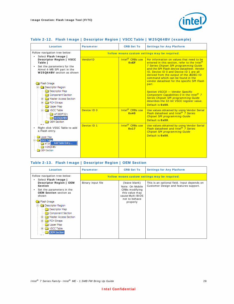
Table 2-11. Flash Image | Descriptor Region | VSCC Table | Add Table Entry
Location Parameter CRB Set To Settings for Any Platform
Follow navigation tree below:• Select the Flash Image tab• Select Flash Image |
Descriptor Region | VSCC Table
• Right click on VSCC Table to add entry name
ADD Table Entry Value Intel® CRB use W25Q64BV
orAT26DF321
Set this to the name of the SPI Flash device on the target platform.
Note: The AT26DF321 and W25Q64BV entries are created as part of the default FITC template.
Intel® 7 Series Family- Intel® ME - 1.5MB FW Bring Up Guide 28
Intel Confidential
Image Creation: Flash Image Tool (FITC)
Table 2-12. Flash Image | Descriptor Region | VSCC Table | W25Q64BV (example)
Location Parameter CRB Set To Settings for Any Platform
Follow navigation tree below: • Select Flash Image |
Descriptor Region | VSCC Table |
• Set the parameters for the Atmel 4-MB SPI part in the W25Q64BV section as shown
• Right click VSSC Table to add a Flash entry.
Yellow means custom settings may be required.
VendorID Intel® CRBs use 0xEF
For information on values that need to be entered in this section, refer to the Intel® 7 Series Chipset SPI programming Guide and the SPI Flash device datasheet. Vendor ID, Device ID 0 and Device ID 1 are all derived from the output of the JEDEC ID command which can be found in the vendor datasheet for the specific SPI Flash part.
Section VSCC0 — Vendor Specific Component Capabilities 0 in the Intel® 7 Series Chipset SPI programming Guide describes the 32-bit VSCC register value.Default is 0x00.
Device ID 0 Intel® CRBs use 0x40
Use values obtained by using Vendor Serial Flash datasheet and Intel® 7 Series Chipset SPI programming Guide Default is 0x00.
Device ID 1 Intel® CRBs use 0x17
Use values obtained by using Vendor Serial Flash datasheet and Intel® 7 Series Chipset SPI programming GuideDefault is 0x00.
Table 2-13. Flash Image | Descriptor Region | OEM Section
Location Parameter CRB Set To Settings for Any Platform
Follow navigation tree below:• Select Flash Image |
Descriptor Region | OEM Section
• Set the parameters in the OEM Section section as shown
Yellow means custom settings may be required.
Binary input file (leave blank)Note: On Mobile CRBs modifying this value may
cause Multi-BIOS not to behave
properly
This is an optional field. Input depends on Customer Design and features support.

Intel® 7 Series Family- Intel® ME - 1.5MB FW Bring Up Guide 29
Intel Confidential
Image Creation: Flash Image Tool (FITC)
2.4.1 Set Up Soft-Straps
Table 2-14. Flash Image | Descriptor Region | PCH Straps | PCH Strap 0
Location Parameter CRB Set To Settings for Any Platform
Follow navigation tree below:• Select the Flash Image tab• Select Flash Image |
Descriptor Region | PCH Straps | PCH Strap 0
• Set the parameters in the PCH Strap 0 section as shown
Yellow means custom settings may be required.
BIOS Boot Block Size 64KB BIOS Boot Block (BBB) is bare minimum BIOS code required to boot a platform. This soft-strap allows for proper address bit to be inverted as required by BBB Size. 64KB (default) = Invert A16 if Top Swap is set 128KB = Invert A17 if Top Swap is set 256KB = Invert A18 if Top Swap is setIf BIOS is stored in a separate SPI Flash device or in FWH (see Configurations “B”, “C”, and “D” in Appendix A then leave this parameter at 64KB.Note: This must be determined by the target platform BIOS developer.
DMI RequesterID Check Disable false
Indicates if RequesterID checking during DMI accesses is disabled. This parameter should only for server platforms that contain multiple Processors.false (default) = Single Processor Platform true = Multiple Processor PlatformNote: A quad/dual core processor counts as a single processor for this parameter.
MACsec Disable false This setting should be set to ‘false’ to enable MACsec. The “MACsec ready” bit in the ME descriptor region should be enabled for support.• This bit must be set in the manufacturing plant and cannot be changed aftershipment. Note: If MACsec is enabled in IT infrastructure will not function properly. See ‘CDI #461067’ for further details.Note: This field is read only if Intel® integrated LAN is disabled. See Table 2-2
LANPHYPC_GP12_SEL 1 1 (default) = Only required if target platform has Intel® wired LAN and PCH GP12 is used as LAN_PHYPC for Intel® LAN.0 = PCH GP12 is used as General Purpose Input/Output (GPIO) pin. Must be 0 if Third-party LAN and no Intel® wired LAN is present.Note: Please consult with the target hardware designer to determine this setting.
Intel® ME SMBus Enable true true = Set for all platformsIntel® ME SMBus Frequency
100kHz Treat as reserved.
SMLink0 Enable true true (default) = Intel® LAN is present false = Third-party LAN is present
SMLink0 Frequency Fast Mode Treat as reserved.SMLink1 Enable Mobile and
Desktop CRBuses true
true (default) = SMLink1 is being used by EC/SIO/BMC for Thermal Reporting.false = Set for all other platforms
SMLink1 Frequency 100kHz Treat as reserved.Chipset Config true Treat as reserved.

Intel® 7 Series Family- Intel® ME - 1.5MB FW Bring Up Guide 30
Intel Confidential
Image Creation: Flash Image Tool (FITC)
Table 2-15. Flash Image | Descriptor Region | PCH Straps | PCH Strap 2
Location Parameter CRB Set To Settings for Any Platform
Follow navigation tree below:• Select the Flash Image tab• Select Flash Image |
Descriptor Region | PCH Straps | PCH Strap 2
• Set the parameters in the PCH Strap 2 section as shown
Yellow means custom settings may be required.
SMBus I2C Address Enable (SMBI2CEN)
false Treat as reserved.
SMBus I2C Address (SMBI2CA)
0x00 Treat as reserved.
Intel® ME SMBus MCTP Address Enable
false true = Using Intel® Anti-Theft Technology with a 3G NICfalse = Not using Intel®Anti-Theft Technology with a 3G NIC
Intel® ME SMBus MCTP Address
0x2B This field must be set to an address value if using Intel® Anti-Theft Technology with a 3G NIC0x00 = Not using Intel®Anti-Theft Technology with a 3G NICNote: Please consult the target hardware designer to determine this setting.
Intel® ME SMBus ASD Address Enable (MESMASDEN)
false Treat as reserved.
Intel® ME SMBus ASD Address (MESMASDA)
0x00 Treat as reserved.
Table 2-16. Flash Image | Descriptor Region | PCH Straps | PCH Strap 4
Location Parameter CRB Set To Settings for Any Platform
Follow navigation tree below:• Select the Flash Image tab• Select Flash Image |
Descriptor Region | PCH Straps | PCH Strap 4
• Set the parameters in the PCH Strap 4
Yellow means custom settings may be required.
GbE PHY SMBus Address 0x64 Intel® wired LAN PHY SMBus address. No change required for this soft-strap value.
GbE MAC SMBus Address 0x70 Intel® wired LAN MAC SMBus address. No change required for this soft-strap value.
GbE MAC SMBus Address Enable
true true (default) = Intel® integrated LAN is enabled false = Third-party LAN is presentNote: This field is read only if Intel® integrated LAN is disabled. See Table 2-2
PHY Connectivity 10: PHY on SMLink0
10: PHY Connectivity = Intel® LAN is present 00: No PHY Connected (default) = Third-party LAN is present only Note: This field is read only if Intel® integrated LAN is disabled. See Table 2-2

Intel® 7 Series Family- Intel® ME - 1.5MB FW Bring Up Guide 31
Intel Confidential
Image Creation: Flash Image Tool (FITC)
Table 2-17. Flash Image | Descriptor Region | PCH Straps | PCH Strap 7
Location Parameter CRB Set To Settings for Any Platform
Follow navigation tree below:• Select the Flash Image tab.• Select Flash Image |
Descriptor Region | PCH Straps | PCH Strap 7
• Set the parameters in the PCH Strap 7
Intel® ME SMBus Subsystem Vendor & Device ID for ASF2
0x00000000 Treat as reserved.

Intel® 7 Series Family- Intel® ME - 1.5MB FW Bring Up Guide 32
Intel Confidential
Image Creation: Flash Image Tool (FITC)
Table 2-18. Flash Image | Descriptor Region | PCH Straps | PCH Strap 9
Location Parameter CRB Set To Settings for Any Platform
Follow navigation tree below:• Select the Flash Image tab• Select Flash Image |
Descriptor Region | PCH Straps | PCH Strap 9
• Set the parameters in the PCH Strap 9
Yellow means custom settings may be required.
PCHHOT# or SML1ALERT# Select
SML1ALERT# This strap determines the native mode operation of GPIO74.PCHHOT#is used to indicate the PCH temperature out of bounds condition to an external agent such as BMC or EC, when PCH temperature is greater than value programmed by BIOS.SML1ALERT# allows the ME SMBus controller to alert an external controller connected to the SMLink interface when it wants to talk to the external controller.
Subtractive Decode Agent Enable
true true = A PCI Bridge chip is connected to the PCHfalse (default) = A PCI Bridge chip is not connected to the PCHNote: Please consult the target hardware designer to determine this setting
Intel® PHY Over PCI Express Enable (PHY_ PCIE_EN)
true true (default) = Intel® LAN is present false = Third-party LAN is present
Intel® PHY PCIe Port Select (PHY_PCIEPORTSEL)
101:Port 6 Only necessary if Intel® LAN is present.101 = Third-party LAN is present (don’t care setting)Note: This field is read only if Intel® integrated LAN is disabled. See Table 2-2
000 = Port 1 001 = Port 2 010 = Port 3 011 = Port 4
100 = Port 5 101 = Port 6 110 = Port 7 111 = Port 8Default is 101.
Chipset Config true Must be set to true (1b).
DMI Lane Reversal false Note: Please consult the target hardware designer to determine this setting
When using Small Form Factor CRB platforms (SKU QS77 and UM77), Set this value to ‘true’.
PCIe Lane Reversal 2 false This parameter must reflect platform topology.Note: This parameter can only be set to true if PCIe Port configuration 2 is set to 1x4.
PCIe Lane Reversal 1 false This parameter must reflect platform topology.Note: This parameter can only be set to true if PCIe Port configuration 1 is set to 1x4.
PCIe Port Configuration 2 00: 4x1 Ports 5-8 (x1)
Note: Please consult the target hardware designer to determine this setting
PCIe Port Configuration 1 00: 4x1 Ports 1-4 (x1)
Note: Please consult the target hardware designer to determine this setting

Intel® 7 Series Family- Intel® ME - 1.5MB FW Bring Up Guide 33
Intel Confidential
Image Creation: Flash Image Tool (FITC)
Table 2-19. Flash Image | Descriptor Region | PCH Straps | PCH Strap 10
Location Parameter CRB Set To Settings for Any Platform
Follow navigation tree below: • Select the Flash Image tab• Select Flash Image |
Descriptor Region | PCH Straps | PCH Strap 10
• Set the parameters in the PCH Strap 10 section as shown
Yellow means custom settings may be required.
ME boot from Flash false(grayed out)
false (default) = No ME Region binary loaded, or ME Region binary does not contain ME ROM bypass imageNote: On B0 and later PCH stepping parts this setting should be set to ‘false’
Reserved false This value must be set to ‘false’
ME Debug SMBus Emergency Mode Enable
false Note: This option should not be enabled. Treat as Reserved.
ME Debug SMBus Emergency Mode Address
0x00 0x38 = Recommended SMBus address for ME Debug Set for non-production/debug platforms.0x00 = Set for production platforms.
ICC Boot Profile 0 Specifies which clock control parameter set is to be used by the final generated SPI Flash binary image by the target platform at boot time.SPI Flash binary images across multiple board designs are expected to contain the same block of clock control parameters, up to 8 sets total.The ‘Record #’ refers to records created under the Configuration Tab, Flash Image | ME Region | Configuration | ICC Data.Default is 0.
ME Reset Capture on CL_RST1#
false Determines if ME reset assert/de-assert can be observed on PCH pin CL_RST1#.true = ME reset assert/de-assert can be observed on PCH pin CL_RST1#false = CL_RST1# usage is available as per Intel® 7 Series / 216 Chipset Family EDS
ICC Boot Profile Selected By Soft Strap
true Specifies if the ICC Boot Profile is selected by Soft Strap or controlled by BIOS.
Deep Sx Enable false true (default) = Platform HWconfiguration supports DSW rail and entryinto Deep S3, S4 / S5.false = For platform that do not supportDSW rail or Deep S3, S4 / S5.Note: Please consult with the target hardware designer to determine this setting.Note: See Section 5.3 – for details on configuring this option.
ME Debug LAN Emergency Mode
false true = Enables ME Debug LAN Emergency Mode logging. Set for non-production/debug platforms.false (default) = Set for production platforms

Intel® 7 Series Family- Intel® ME - 1.5MB FW Bring Up Guide 34
Intel Confidential
Image Creation: Flash Image Tool (FITC)
Table 2-20. Flash Image | Descriptor Region | PCH Straps | PCH Strap 11
Location Parameter CRB Set To Settings for Any Platform
Follow navigation tree below:• Select the Flash Image tab• Select Flash Image |
Descriptor Region | PCH Straps | PCH Strap 11
• Set the parameters in the PCH Strap 11 section as shown
Yellow means custom settings may be required.
SMLink1 I2C Target Address Enable
CRB uses true true (default) = Enable EC/SIO/BMC to interact Thermal Reporting feature over SMLink1false = Platform has no EC/SIO/BMC on SMLink1
SMLink1 I2C Target Address
CRB uses 0x4C This parameter defines a write address for PCH over SMLink1. Set this to an address supported by EC/SIO/BMC hardware. Note that PCH/Intel® ME acts as slave on SMLink and EC/SIO/BMC acts as master.0x4C (default) = PCH SMBus write address for EC on mobile CRB0x00 = Platform has no EC/SIO/BMC on SMLink1
SMLink1 GP Target Address Enable
CRB uses true true (default) = Enable EC/SIO/BMC to interact Thermal Reporting feature over SMLink1false = Platform has no EC/SIO/BMC on SMLink1
SMLink1 GP Target Address
CRB uses 0x4B This parameter defines a read address for PCH over SMLink1. Set this to an address supported by EC/SIO/BMC hardware. Note that PCH/Intel® ME acts as slave on SMLink and EC/SIO/BMC acts as master.0x4B (default) = PCH SMBus read address for EC on mobile CRB0x00 = Platform has no EC/SIO/BMC on SMLink1

Intel® 7 Series Family- Intel® ME - 1.5MB FW Bring Up Guide 35
Intel Confidential
Image Creation: Flash Image Tool (FITC)
Table 2-21. Flash Image | Descriptor Region | PCH Straps | PCH Strap 15
Location Parameter CRB Set To Settings for Any Platform
Follow navigation tree below:• Select Flash Image |
Descriptor Region | PCH Straps | PCH Strap 15
• Set the parameters in the PCH Strap 15 section as shown
Yellow means custom settings may be required.
SLP_LAN#/GPIO29 Select false true = Enables GPIO29 and disables SLP_LAN# functionality.false =Set to false to use have GPIO behave as SLP_LAN#. Note: This field is read only if Intel® integrated LAN is disabled. See Table 2-2.
SMLink1 Thermal Reporting Select
Desktopfalse
Mobiletruefalse
false = Intel® ME FW will collect temperature from the processor, PCH and DIMMs. It will be available for polling on SMLink1.
Note: ME Thermal Reporting: Advantage = Does not require PECI capability in EC. Disadvantage = no real time temperature alert level control, and no dynamic Sandy Bridge / Ivy Bridge CPU Turbo controls.
— SMLink Thermal Reporting Select = false (default)
— PECI from Sandy Bridge / Ivy Bridge processor is connected to PCH
— BIOS sets Thermal Reporting Control (TRC) MMIO register at TBARB+1Ah to enable ME reporting of processor, PCH, and DIMM temperatures (as appropriate)
— ME thermal reporting PCI device should be enabled for proper interaction with EC, SIO, BMC, or equivalent fan control logic
true = PCH temperature ONLY(1 byte of data) will be available for polling out on SMLink1. Processor and DIMMs temperature monitoring will require an external device.
Note: Platform based Thermal Reporting: Advantage = allows full dynamic Sandy Bridge / Ivy Bridge Turbo control. Disadvantage = Requires EC/BMC with PECI capability.
— SMLink Thermal Reporting Select = true— PECI from Sandy Bridge / Ivy Bridge
processor is connected direct to EC, SIO, BMC, or equivalent fan control logic
— BIOS sets Thermal Reporting Control (TRC) MMIO register at TBARB+1Ah = 0x0, disabling ME reporting of processor, PCH, and DIMM temperatures
— ME thermal reporting PCI device should be disabled
Intel®Integrated LAN Enable
true true = Intel® LAN is enabled false = Intel® LAN is disabledNote: This field is read only if Intel® integrated LAN is disabled. See Table 2-2.
Reserved0 false Treat as reserved.

Intel® 7 Series Family- Intel® ME - 1.5MB FW Bring Up Guide 36
Intel Confidential
Image Creation: Flash Image Tool (FITC)
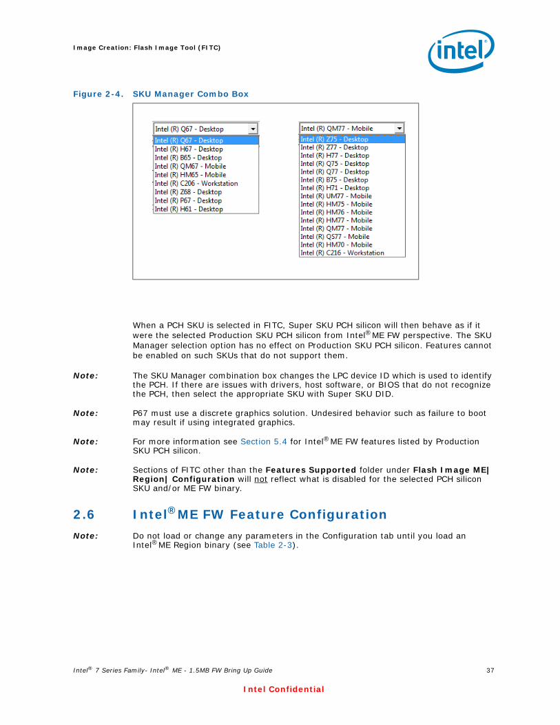
2.5 Configure PCH Silicon SKUUse the SKU Manager Combo Box to select the appropriate platform type for your specific chipset.
For Intel®ME 1.5MB FW, the only valid choices are:
• 7 Series Chipset
— Intel® Z77 Express Chipset— Intel® Z75 Express Chipset — Intel® H77 Express Chipset — Mobile Intel® QS77 Express Chipset— Mobile Intel® HM70 Express Chipset— Mobile Intel® HM77 Express Chipset— Mobile Intel® HM76 Express Chipset— Mobile Intel® HM75 Express Chipset— Mobile Intel® UM77 Express Chipset
• Intel® 6 Series Chipset
— Intel® P67 Express Chipset — Intel® H67 Express Chipset — Intel® H61 Express Chipset — Intel® Z68 Express Chipset — Mobile Intel® HM65 Express Chipset
Table 2-22. Flash Image | Descriptor Region | PCH Straps | PCH Strap 17
Location Parameter CRB Set To Settings for Any Platform
Follow navigation tree below:• Select Flash Image |
Descriptor Region | PCH Straps | PCH Strap 17
• Set the parameters in the PCH Strap 17 section as shown
Yellow means custom settings may be required.
BTM/FCIM Select Full Clock Integrated Mode
If PCH clock boot mode is specified by soft strap then this parameter specifies whether the PCH clocks boot in Full Clock Integrated Mode (FCIM) or Buffer Through Mode (BTM).
NOTE: Buffer Through Mode (BTM) is NOT POR mode supported by Intel® 7 Series/C216 Chipset Family and it will not be validated by Intel®.
Intel® 7 Series Family- Intel® ME - 1.5MB FW Bring Up Guide 37
Intel Confidential
Image Creation: Flash Image Tool (FITC)
When a PCH SKU is selected in FITC, Super SKU PCH silicon will then behave as if it were the selected Production SKU PCH silicon from Intel®ME FW perspective. The SKU Manager selection option has no effect on Production SKU PCH silicon. Features cannot be enabled on such SKUs that do not support them.
Note: The SKU Manager combination box changes the LPC device ID which is used to identify the PCH. If there are issues with drivers, host software, or BIOS that do not recognize the PCH, then select the appropriate SKU with Super SKU DID.
Note: P67 must use a discrete graphics solution. Undesired behavior such as failure to boot may result if using integrated graphics.
Note: For more information see Section 5.4 for Intel®ME FW features listed by Production SKU PCH silicon.
Note: Sections of FITC other than the Features Supported folder under Flash Image ME| Region| Configuration will not reflect what is disabled for the selected PCH silicon SKU and/or ME FW binary.
2.6 Intel®ME FW Feature ConfigurationNote: Do not load or change any parameters in the Configuration tab until you load an
Intel®ME Region binary (see Table 2-3).
Figure 2-4. SKU Manager Combo Box
Intel® 7 Series Family- Intel® ME - 1.5MB FW Bring Up Guide 38
Intel Confidential
Image Creation: Flash Image Tool (FITC)
2.6.1 Firmware Features and Capabilities
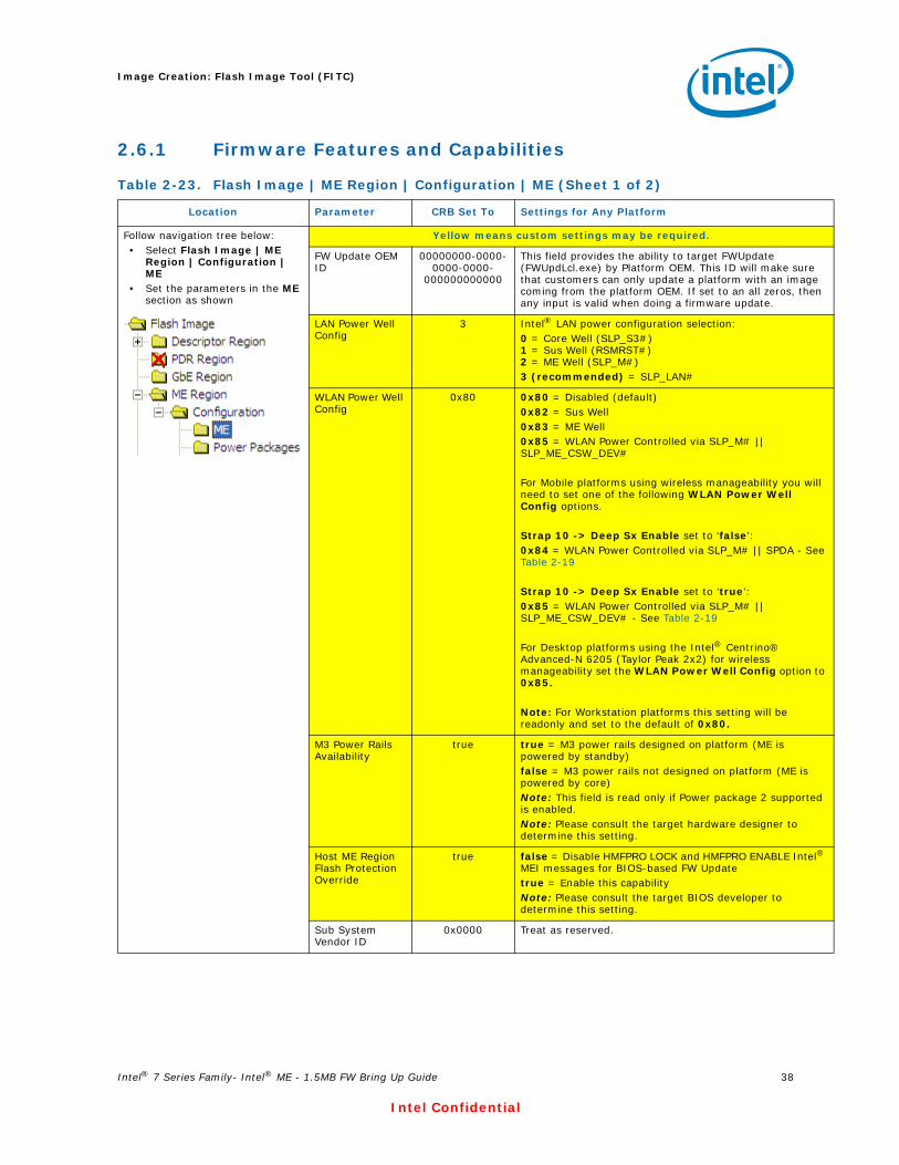
Table 2-23. Flash Image | ME Region | Configuration | ME (Sheet 1 of 2)
Location Parameter CRB Set To Settings for Any Platform
Follow navigation tree below:• Select Flash Image | ME
Region | Configuration | ME
• Set the parameters in the ME section as shown
Yellow means custom settings may be required.
FW Update OEM ID
00000000-0000-0000-0000-
000000000000
This field provides the ability to target FWUpdate (FWUpdLcl.exe) by Platform OEM. This ID will make sure that customers can only update a platform with an image coming from the platform OEM. If set to an all zeros, then any input is valid when doing a firmware update.
LAN Power Well Config
3 Intel® LAN power configuration selection:0 = Core Well (SLP_S3#) 1 = Sus Well (RSMRST#) 2 = ME Well (SLP_M#)3 (recommended) = SLP_LAN#
WLAN Power Well Config
0x80 0x80 = Disabled (default)0x82 = Sus Well0x83 = ME Well0x85 = WLAN Power Controlled via SLP_M# || SLP_ME_CSW_DEV#
For Mobile platforms using wireless manageability you will need to set one of the following WLAN Power Well Config options.
Strap 10 -> Deep Sx Enable set to ‘false’:0x84 = WLAN Power Controlled via SLP_M# || SPDA - See Table 2-19
Strap 10 -> Deep Sx Enable set to ‘true’:0x85 = WLAN Power Controlled via SLP_M# || SLP_ME_CSW_DEV# - See Table 2-19
For Desktop platforms using the Intel® Centrino® Advanced-N 6205 (Taylor Peak 2x2) for wireless manageability set the WLAN Power Well Config option to 0x85.
Note: For Workstation platforms this setting will be readonly and set to the default of 0x80.
M3 Power Rails Availability
true true = M3 power rails designed on platform (ME is powered by standby)false = M3 power rails not designed on platform (ME is powered by core)Note: This field is read only if Power package 2 supported is enabled. Note: Please consult the target hardware designer to determine this setting.
Host ME Region Flash Protection Override
true false = Disable HMFPRO LOCK and HMFPRO ENABLE Intel® MEI messages for BIOS-based FW Updatetrue = Enable this capabilityNote: Please consult the target BIOS developer to determine this setting.
Sub System Vendor ID
0x0000 Treat as reserved.

Intel® 7 Series Family- Intel® ME - 1.5MB FW Bring Up Guide 39
Intel Confidential
Image Creation: Flash Image Tool (FITC)
PROC_MISSING No onboard glue logic
Only set if there is glue logic present on the board to enable if the processor is missing. Note: This field is read only if a Mobile SKU is selected in the SKU Manager pull down box.Note: Please consult the target hardware designer to determine this setting.
Processor Emulation
No EmulationNo Emulation
Set this parameter to the type of processor that the target system will use during production. This field will emulate that processor class for pre-production silicon.
OEM Tag 0x00000000 This value allows OEMs to set a unique number value in their firmware images to allow for easier identification.
Hide FW Update Control
false This option determines if the MEBx FW Update is visible or hidden from end users.
‘false’ - The MEBx FW update option will be visible to end users.‘true’ - The MEBx FW update option will not be visible to the end user.
Debug Si Features
0x00000000 Allows OEM Control to enable FW features to assist with the debug of the platform. This control has no effect if used on production silicon.
Bit 0: Disable time-out on BIOS HECI messagingBit 1: Disable FW watchdog timer
Prod Si Features 0x00000000 Allow OEM Control to enable FW features to assist with the production platform.
Bit 1: Disable FW watchdog timer
M3 Autotest Enabled
false This enables Intel®ME FW M3 auto test during platform early boot.
‘false’ - The Intel®ME FW will not run M3 tests during first boot afterplattorm image flash.‘true’ - The Intel®ME FW will run M3 tests during first boot afterplatform image flash.
IndependentFirmwareRecovery Enable
true This option determines if Independent Firmware Recoveryis enabled.
‘false’ - Independent Firmware Recovery is disabled in thefirmware.‘true’ - Independent Firmware Recovery is enabled in thefirmware.
Table 2-23. Flash Image | ME Region | Configuration | ME (Sheet 2 of 2)
Location Parameter CRB Set To Settings for Any Platform

Intel® 7 Series Family- Intel® ME - 1.5MB FW Bring Up Guide 40
Intel Confidential
Image Creation: Flash Image Tool (FITC)
Since 1.5MB FW does not support “Manageability Application” when users select Flash Image | ME Region | Configuration | Manageability Application, the following Warning message will be displayed.
Table 2-24. Flash Image | ME Region | Configuration | Power Packages
Location Parameter CRB Set To Settings for Any Platform
Follow navigation tree below:• Select Flash Image | ME
Region | Configuration | Power Packages
• Set the parameters in the Power Packages section as shown
Yellow means custom settings may be required.
Power Pkg 2 Supported (Desktop: ON in S0, ME Wake in S3, S4-5)
false Intel®false = Set for all platforms (not supported on 1.5MB FW)
Default Power Package 1 Select the default Power Package from the available packages. Set to 1 for all platforms.
Note: The ON in S0 package is automatically selected as default in the base firmware binary.
Table 2-25. Flash Image | ME Region | Configuration | Features Supported
Location Parameter CRB Set To Settings for Any Platform
Follow navigation tree below:• Select Flash Image | ME
Region | Configuration | Features Supported
• Set the parameters in the Features Supported section as shown
Yellow means custom settings may be required.
Enable Intel® Standard Manageability; Disable Intel® AMT
Yes
Note: Setting any of these options to ‘Yes’ will permanently disable that specific feature.Once the feature is disabled in this manner only re-Flashing the ME region can re-enable the feature.Fields are read only if the feature is not supported by respective PCH SKU selected by PCH SKU pull down (see Section 2.5).
Intel® Manageability Application Permanently Disabled?
Yes
PAVP Permanently Disabled
No
KVM Permanently Disabled?
Yes
TLS Permanently Disabled?
No
Intel® Anti-Theft Technology Permanently disabled
No
Intel® ME Network Service Permanently disabled
No
Service Advertisement and Discovery Permanently Disabled
Yes
Intel® Manageability Application Enable/Disable
Disabled Disabled (not supported on 1.5MB FW)
Note: The Feature supported settings shown above are an example.

Intel® 7 Series Family- Intel® ME - 1.5MB FW Bring Up Guide 41
Intel Confidential
Image Creation: Flash Image Tool (FITC)
Figure 2-5. Manageability Application Warning
Table 2-26. Flash Image | ME Region | Configuration | Intel® Anti-Theft Technology
Location Parameter CRB Set To Settings for Any Platform
Follow navigation tree below:• Select Flash Image | ME
Region | Configuration | Intel® Anti-Theft Technology
• Set the parameters in the Intel® Anti-Theft Technology section as shown
Yellow means custom settings may be required.
Allow Unsigned Assert Stolen
false Treat as reserved.
Intel(R) Anti-Theft BIOS Recovery Timer
Disabled This timer will enable a 30 minute window to allow a firmware/BIOS reflash before the system is powered down.

Intel® 7 Series Family- Intel® ME - 1.5MB FW Bring Up Guide 42
Intel Confidential
Image Creation: Flash Image Tool (FITC)
Flash Protection Override Policy Hard
Allowed When AT Not
Provisioned
This option determines if the ME will enter a disabled state to allow full SPI device re-flashing when the manufacturing override jumper (HMFPRO) is set.
Always Allowed - Full SPI re-flash will always be allowed regardless of Intel®AT enrollment state.
Allowed When AT Not Provisioned - Full SPI re-flash allowed if Intel®AT has not been enrolled.
Flash Protection Override Policy Soft
Allowed When AT Not
Provisioned
This option determines if the ME will enter a disabled state via BIOS based MEI messages and allow ME only region re-flash.
Always Allowed - Intel®ME region re-flash will always be allowed regardless of Intel®AT enrollment state.
Allowed When AT Not Provisioned - Intel®ME region re-flash allowed if Intel®AT has not been enrolled.
Table 2-26. Flash Image | ME Region | Configuration | Intel® Anti-Theft Technology
Location Parameter CRB Set To Settings for Any Platform

Intel® 7 Series Family- Intel® ME - 1.5MB FW Bring Up Guide 43
Intel Confidential
Image Creation: Flash Image Tool (FITC)
Table 2-27. Flash Image | ME Region | Configuration | ME Debug Event Service
Location Parameter
ME Debug Enabled SPI
Critical Logging* (FITC
Default)
Full ME Debug Enabled Settings for Any Platform
Follow navigation tree below:• Select Flash Image | ME Region |
Configuration | ME Debug Event Service
• Set the parameters in the ME Debug Event Service section as shown
Basic Filter configuration:
Advanced Filter configuration (LAN):
Advanced Filter configuration (SMBus):
Green means custom settings may be required (for enabling ME Debug only)Error Filter Critical AllLogging Interface - Network
false true Set to true only for platforms with Intel® LAN.
Logging Interface - SMBus
false false Can be set to true for platforms with no Intel® LAN. May also be set to true if ME Debug logging through SMBus is desired.
Logging Interface - Flash
true false Note: This should only be used with the Critcal filter setting options from the first column (ME Debug Enabled SPI Logging).
Logging Interface - PRAM
false false
Buffer Size 0 24 Default is 0.Buffer Mode Blocking Buffered Note: Delayed Flush is not
supported.
Note: Buffered mode should never be used when using SPI logging.
Source IP Address
10.2.0.2 10.2.0.2
Destination IP Address
10.2.0.255 10.2.0.255
Destination MAC Address
0C FF 17 22 FF 2D
0C FF 17 22 FF 2D
This is the MAC address of the SUT.
Slave Address Enable
false true
Slave Address 0x00 0x56 Default is 0x56.Event Filters Filter Group 1:
0x00000001Filter Group 76: 0x000000FE
All other values set to:
0x00000000
BasicFilter Group 1: 0x00000001Filter Group 5: 0x00000003Filter Group 6: 0x000F0000
Filter Group 70: 0x00000001
Advanced (Intel® LAN)Filter Group 1: 0x00000001Filter Group 4: 0x000003F6Filter Group 5: 0x00000003Filter Group 6: 0x000F0000
Filter Group 70: 0x00000001
Advanced (SMBus)
Filter Group 1: 0x00000001Filter Group 4: 0x000003F6Filter Group 5: 0x00000003Filter Group 6: 0x000F0000
Filter Group 70: 0x00000001
Note: To enable Filter groups 74 and 75 add a 1 value.

Intel® 7 Series Family- Intel® ME - 1.5MB FW Bring Up Guide 44
Intel Confidential
Image Creation: Flash Image Tool (FITC)
Table 2-28. Flash Image | ME Region | Configuration | Setup and Configuration
Location Parameter CRB Set To Settings for Any Platform
Follow navigation tree below:• Select Flash Image | ME
Region | Configuration | Setup and Configuration
• Set the parameters in the Setup and Configuration section as shown
Yellow means custom settings may be required.ODM ID used by Intel(R) Services
0x00000000 These fields are used by Intel® Services. Intel® Identity Protection Technology (Intel® IPT) use ODM ID field only (for platform identification between the OEM and the ISBV).
System Integrator ID used by Intel(R) Services
0x00000000
Reserved ID used by Intel(R) Services
0x00000000
MCTP static EIDs 0x920030 Defines the ME 8 bit MCTP endpoint IDs for Each SMBus segment. Only bits 0-7 are supported to be modified. Bits 8-23 must be left to 0x9200
MCTP Info 3G 0x02 This field must be set to the 7-bit SMBus address of the 3G NIC. Only supported if using Intel® Anti-Theft Technology with a 3G NIC
Permit Period Timer Resolution
Days Treat as reserved.
PKI DNS Suffix Leave Blank Treat as reserved.OEM Default Certificate Active
false Treat as reserved.
OEM Default Certificate Friendly Name
Leave Blank Treat as reserved.
OEM Default Certificate Stream
Leave Blank Treat as reserved.
OEM Default Certificate 2-5 Active
false Treat as reserved.
OEM Default Certificate 2-5 Friendly Name
Leave Blank Treat as reserved.
OEM Default Certificate 2-5 Stream
Leave Blank Treat as reserved.
OEM Customizable Certificate 1-3 Active
false Treat as reserved.
OEM Customizable Certificate 1-3 Friendly Name
Leave Blank Treat as reserved.
OEM Customizable Certificate 1-3 Stream
Leave Blank Treat as reserved.
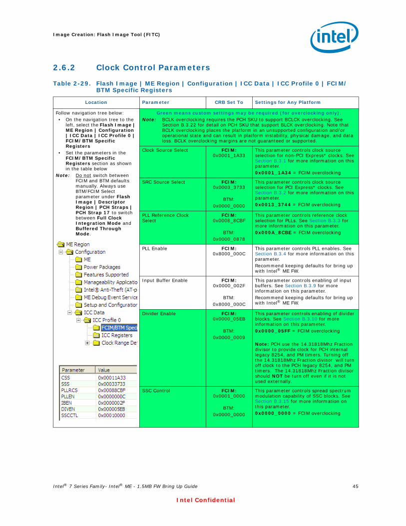
Intel® 7 Series Family- Intel® ME - 1.5MB FW Bring Up Guide 45
Intel Confidential
Image Creation: Flash Image Tool (FITC)
2.6.2 Clock Control Parameters
Table 2-29. Flash Image | ME Region | Configuration | ICC Data | ICC Profile 0 | FCIM/BTM Specific Registers
Location Parameter CRB Set To Settings for Any Platform
Follow navigation tree below:• On the navigation tree to the
left, select the Flash Image | ME Region | Configuration | ICC Data | ICC Profile 0 | FCIM/BTM Specific Registers
• Set the parameters in the FCIM/BTM Specific Registers section as shown in the table below
Note: Do not switch between FCIM and BTM defaults manually. Always use BTM/FCIM Select parameter under Flash Image | Descriptor Region | PCH Straps | PCH Strap 17 to switch between Full Clock Integration Mode and Buffered Through Mode.
Green means custom settings may be required (for overclocking only).Note: BCLK overclocking requires the PCH SKU to support BCLCK overclocking. See
Section B.3.22 for detail on PCH SKU that support BLCK overclocking. Note that BCLK overclocking places the platform in an unsupported configuration and/or operational state and can result in platform instability, physical damage, and data loss. BCLK overclocking margins are not guaranteed or supported.
Clock Source Select FCIM: 0x0001_1A33
This parameter controls clock source selection for non-PCI Express* clocks. See Section B.3.1 for more information on this parameter.0x0001_1A34 = FCIM overclocking
SRC Source Select FCIM: 0x0003_3733
BTM:0x0000_0000
This parameter controls clock source selection for PCI Express* clocks. See Section B.3.2 for more information on this parameter.0x0013_3744 = FCIM overclocking
PLL Reference Clock Select
FCIM: 0x0008_8CBF
BTM:0x0000_0878
This parameter controls reference clock selection for PLLs. See Section B.3.3 for more information on this parameter.0x000A_8CBE = FCIM overclocking
PLL Enable FCIM: 0x8000_000C
This parameter controls PLL enables. See Section B.3.4 for more information on this parameter.Recommend keeping defaults for bring up with Intel® ME FW.
Input Buffer Enable FCIM: 0x0000_002F
BTM:0x8000_000C
This parameter controls enabling of input buffers. See Section B.3.9 for more information on this parameter.Recommend keeping defaults for bring up with Intel® ME FW.
Divider Enable FCIM: 0x0000_05EB
BTM:0x0000_0009
This parameter controls enabling of divider blocks. See Section B.3.10 for more information on this parameter.0x0000_05FF = FCIM overclocking
Note: PCH use the 14.31818Mhz Fraction divisor to provide clock for PCH internal legacy 8254, and PM timers. Turning off the 14.31818Mhz Fraction divisor will turn off clock to the PCH legacy 8254, and PM timers. The 14.31818Mhz Fraction divisor should NOT be turn off even if it is not used externally.
SSC Control FCIM: 0x0001_0000
BTM:0x0000_0000
This parameter controls spread spectrum modulation capability of SSC blocks. See Section B.3.15 for more information on this parameter.0x0000_0000 = FCIM overclocking
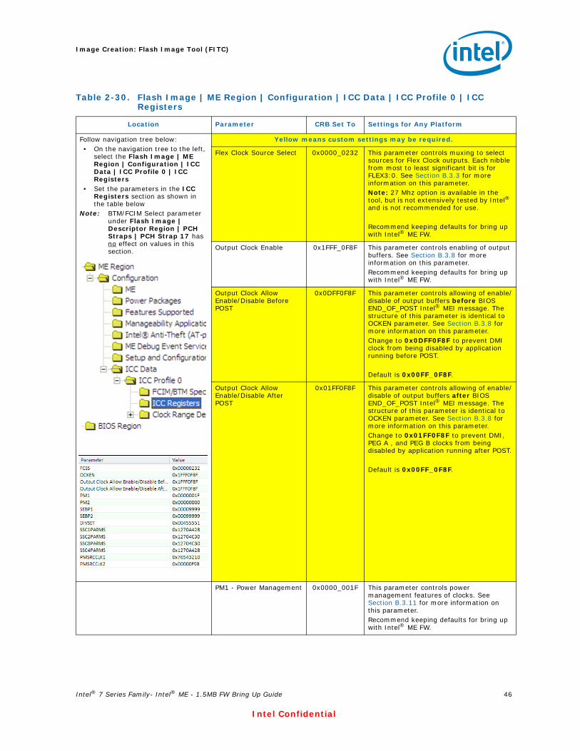
Intel® 7 Series Family- Intel® ME - 1.5MB FW Bring Up Guide 46
Intel Confidential
Image Creation: Flash Image Tool (FITC)
Table 2-30. Flash Image | ME Region | Configuration | ICC Data | ICC Profile 0 | ICC Registers
Location Parameter CRB Set To Settings for Any Platform
Follow navigation tree below:• On the navigation tree to the left,
select the Flash Image | ME Region | Configuration | ICC Data | ICC Profile 0 | ICC Registers
• Set the parameters in the ICC Registers section as shown in the table below
Note: BTM/FCIM Select parameter under Flash Image | Descriptor Region | PCH Straps | PCH Strap 17 has no effect on values in this section.
Yellow means custom settings may be required.
Flex Clock Source Select 0x0000_0232 This parameter controls muxing to select sources for Flex Clock outputs. Each nibble from most to least significant bit is for FLEX3:0. See Section B.3.3 for more information on this parameter.Note: 27 Mhz option is available in the tool, but is not extensively tested by Intel® and is not recommended for use.
Recommend keeping defaults for bring up with Intel® ME FW.
Output Clock Enable 0x1FFF_0F8F This parameter controls enabling of output buffers. See Section B.3.8 for more information on this parameter.Recommend keeping defaults for bring up with Intel® ME FW.
Output Clock Allow Enable/Disable Before POST
0x0DFF0F8F This parameter controls allowing of enable/disable of output buffers before BIOS END_OF_POST Intel® MEI message. The structure of this parameter is identical to OCKEN parameter. See Section B.3.8 for more information on this parameter.Change to 0x0DFF0F8F to prevent DMI clock from being disabled by application running before POST.
Default is 0x00FF_0F8F.
Output Clock Allow Enable/Disable After POST
0x01FF0F8F This parameter controls allowing of enable/disable of output buffers after BIOS END_OF_POST Intel® MEI message. The structure of this parameter is identical to OCKEN parameter. See Section B.3.8 for more information on this parameter.Change to 0x01FF0F8F to prevent DMI, PEG A , and PEG B clocks from being disabled by application running after POST.
Default is 0x00FF_0F8F.
PM1 - Power Management 0x0000_001F This parameter controls power management features of clocks. See Section B.3.11 for more information on this parameter.Recommend keeping defaults for bring up with Intel® ME FW.

Intel® 7 Series Family- Intel® ME - 1.5MB FW Bring Up Guide 47
Intel Confidential
Image Creation: Flash Image Tool (FITC)
PM2 - Power Management 0x0000_0000 This parameter controls power management CLKRUN for PCI clocks. See Section B.3.12 for more information on this parameter.
Yellow means custom settings may be required.
SEBP1 0x0000_9999 This parameter controls double/single load series resistance and slew rate for FLEX clocks. See Section B.3.13 for more information on this parameter.Recommend keeping defaults for bring up with Intel® ME FW.
SEBP2 0x0009_9999 This parameter controls double/single load series resistance and slew rate for PCI clocks. See Section B.3.14 for more information on this parameter.Recommend keeping defaults for bring up with Intel® ME FW.
DIVSET 0x0045_5551 Treat as reserved.
PI12BiasParms 0x0888_0888 This is a Chipset Configuration (PCHCFG) parameter.0x0000_0888 = FCIM overclocking
SSC1PARMS 0x1270_A428 Treat as reserved.
SSC2PARMS 0x1270_4C30 Note: For platform that support Wimax Friendly Clocking- change this registers setting to 0x1270_F418otherwise treat this registers as reserved and use default valueFor more information on PCH SKU that support Wimax Friendly Clocking, see appendix B.3.22
SSC3PARMS 0x1270_4C30 Treat as reserved.
SSC4PARMS 0x1270_A428 Treat as reserved.
SSC2OCPARMS 0x0000_0000 Note: or platform that support Wimax Friendly Clocking - change this registers setting to 0x0000_0300otherwise treat this registers as reserved and use default valueFor more information on PCH SKU that support Wimax Friendly Clocking, see appendix B.3.22
PMSRCCLK1 0x7654_3210 This parameter as signs dynamic CLKRQ# control of SRC clocks. See Section B.3.16 for more information on this parameter.Recommend keeping defaults for bring up with Intel® ME FW.
PMSRCCLK2 0x0000_0F98 This parameter as signs dynamic CLKRQ# control of SRC clocks. See Section B.3.17 for more information on this parameter.Recommend keeping defaults for bring up with Intel® ME FW.
Table 2-30. Flash Image | ME Region | Configuration | ICC Data | ICC Profile 0 | ICC Registers
Location Parameter CRB Set To Settings for Any Platform

Intel® 7 Series Family- Intel® ME - 1.5MB FW Bring Up Guide 48
Intel Confidential
Image Creation: Flash Image Tool (FITC)
Table 2-31. Flash Image | ME Region | Configuration | ICC Data | ICC Profile 0 | Clock Range Definition Record 0 (Sheet 1 of 3)
Location Section Settings for Any Platform
Follow navigation tree below:• On the navigation tree to the
left, select the Flash Image | ME Region | Configuration | ICC Data | ICC Profile 0 | Clock Range Definition Record 0
• Set the parameters in the Clock Range Definition Record 0 section as shown in the table below
Note: ClockDivMin refers to minimum divider value which corresponds to maximum frequency output value. ClockDivMax refers to maximum divider value which corresponds to minimum frequency output value.
Note: Changes are required only if overclocking, otherwise defaults may be used.
Yellow means custom settings may be required.
Green means custom settings may be required (for BCLK overclocking only).Note: BCLK overclocking requires the PCH SKU to support BCLCK overclocking. See
Section B.3.22 for detail on PCH SKU that support BLCK overclocking. Note that BCLK overclocking places the platform in an unsupported configuration and/or operational state and can result in platform instability, physical damage, and data loss. BCLK overclocking margins are not guaranteed or supported.
120/27 MHz Graphics Clock (DIV1-S) Treat as reserved.
Processor or Platform DMICLK (DIV2-S)
Parameters not shown may be treated as reserved.
Parameter CRB Set To
CRB OC Set To Comments
Clock Div Min 0x0C00 0x0400 Recommended maximum clock divider frequency is 100.0 MHz (clock divider minimum = 0xC00).
Change to 0x180 (800 MHz) if BCLK overclocking is being utilized. If the limit for BCLK overclocking is desired to be lower, use one of the following values:0x180 = 800 MHz 0x200 = 600 MHz 0x300 = 400 MHz 0x400 = 300 MHz 0x4CC = 250.1629 MHz 0x554 = 225.2199MHz 0x600 = 200 MHz 0x6DA = 175.1425 MHz 0x800 = 150 MHz 0x892 = 140.0182 MHz 0x93A = 130.0593 MHz 0xA00 = 120 MHz 0xAE8 = 110.0287 MHz 0xB6C = 105.0616 MHz
Clock Div Max 0x0C00 0x0C0E For Basic platform configuration, recommended minimum clock divider frequency is 100MHz clock divider maximum = 0xC00)
For platform that support Wimax friendly clocking or overclocking, the recommended minimum clock divider frequency is 99.5463 MHz (clock divider maximum = 0xC0E).
For more information on PCH SKU that support Wimax Friendly Clocking or overclocking, see appendix B.3.22

Intel® 7 Series Family- Intel® ME - 1.5MB FW Bring Up Guide 49
Intel Confidential
Image Creation: Flash Image Tool (FITC)
SSC Change Allowed Mask
true This determines if the SSC parameters of this clock resource can be controlled by the handled request record.
SSC Spread Mode Control Up
false
SSC Spread Mode Control Center
false
SSC Spread Mode Control Down
true
SSC Spread Percent Max 50
Clock Usage 0x0DF 0x007 Change to indicate processor/DMI (0x007) if overclocking is being utilized.Default is 0x0DF.
Section Settings for Any Platform
Table 2-31. Flash Image | ME Region | Configuration | ICC Data | ICC Profile 0 | Clock Range Definition Record 0 (Sheet 2 of 3)
Location Section Settings for Any Platform

Intel® 7 Series Family- Intel® ME - 1.5MB FW Bring Up Guide 50
Intel Confidential
Image Creation: Flash Image Tool (FITC)
2.7 Build SPI Flash Binary Image
2.7.1 Build SPI Flash Binary ImageIn the main menu select Build | Build Image. The image will be saved in the directory specified by $DestDir parameter and will be named outimage.bin, unless the default Output Directory in Build | Build Settings was changed (see Section 2.1).
PCH DMICLK (DIV3) Make changes below only if overclocking.Parameters not shown may be treated as reserved.
Parameter CRB Default Comments
Clock Div Min 0x0C00 0x0C00 Recommended maximum clock divider frequency is 100.0 MHz (clock divider minimum = 0xC00).
Clock Div Max 0x0C00 0x0C0E For Basic platform configuration, recommended minimum clock divider frequency is 100MHz clock divider maximum = 0xC00)
For platform that support Wimax friendly clocking or overclocking, the recommended minimum clock divider frequency is 99.5463 MHz (clock divider maximum = 0xC0E).
• For more information on PCH SKU that support Wimax Friendly Clocking or overclocking, see appendix B.3.22
SSC Change Allowed Mask
true This determines if the SSC parameters of this clock resource can be controlled by the handled request record.
SSC Spread Mode Control Up
false
SSC Spread Mode Control Center
false
SSC Spread Mode Control Down
true
SSC Spread Percent Max 50
Clock Usage 0x000 0x0D8 Change to indicate PCH PCI Express* and PCI (0x0D8) if overclocking is being utilized.Default is 0x000.
Section Settings for Any Platform
120 MHz SSSC Graphics Clock (DIV4) Treat as reserved.
Table 2-31. Flash Image | ME Region | Configuration | ICC Data | ICC Profile 0 | Clock Range Definition Record 0 (Sheet 3 of 3)
Location Section Settings for Any Platform

Intel® 7 Series Family- Intel® ME - 1.5MB FW Bring Up Guide 51
Intel Confidential
Image Creation: Flash Image Tool (FITC)
2.7.2 Save Your SettingsIn the main menu select File | Save As…. Select a name and location for the XML file that contains all the settings configured thus far. It is recommended that you save this file in your [root)]\Tools\System Tools\Flash Image Tool directory for easy access.
Assuming that the custom settings file was saved as customfile.xml to the FITC directory ([root)]\Tools\System Tools\Flash Image Tool), then these settings could be loaded in the FITC GUI itself using the main menu option File | Load….
Note: Previous platform (ie. Ibex Peak) generations of the FITC tool required multiple configuration files to be edited and saved. For this generation, only one configuration file (customfile.xml) is required.
This custom settings file could also be used to generate an SPI Flash binary image using the command line, with a command of the form:
Example usage: > fitc.exe newfiletmpl.xml /o .\temp.bin /b
where:
• <xml_file> — The XML configuration file saved when configuring FITC.
• /o <file> — The path and filename where the image will be saved. This command overrides the 'Output path' in the XML file.
• /b — Automatically builds the Flash image. The FIT GUI will not be displayed when this flag is set, since FIT will run in auto-build mode. Error messages will be displayed by FITC, if necessary.
2.7.3 Protect Saved Configuration XML FileTo avoid custom-configured values from ever overwritten when loading new binaries files (ie: when loading binaries into BIOS, GbE and ME regions in FITC) do the following (see Figure 2-7):
• After building the SPI Flash binary image and saving your configuration, close Flash Image Tool
Figure 2-6. Build | Build Image
fitc.exe [xml_file] [/o <file>] /b

Intel® 7 Series Family- Intel® ME - 1.5MB FW Bring Up Guide 52
Intel Confidential
Image Creation: Flash Image Tool (FITC)
• Right-click on the saved FITC configuration XML file (customfile.xml) and select Properties
• Check the Read-Only checkbox and click OK
§ §
Figure 2-7. Protecting FITC Configuration XML File

Intel® 7 Series Family - Intel® ME - 1.5MB FW Bring Up Guide 52
Intel Confidential
Image Creation: Flash Image Tool Wizard
3 Image Creation: Flash Image Tool Wizard
Flash Image Tool (FITC) can be used to generate either a full SPI Flash binary image with Descriptor, GbE, BIOS, and Intel® ME Regions. Additionally, it can be used to create a simple image containing only the Intel® ME Region only for use with custom SPI Flash binary image assembly solutions. Use the steps shown in following sections.
After this image has been created, it will need to be burned onto the target platform’s SPI Flash device(s). Section 4, “Programming SPI Flash Devices and Checking Firmware Status” later in this document provides steps to do this.
There are two different interfaces for this tool. A wizard mode and an advanced mode:
• For the wizard mode “FITC Wizard”, please continue with this section. FITC Wizard is intended to streamline the Flash image creation process and is designed for ease of use. Most users should use this mode.
• For the advanced mode “FITC”, please see Section 2.
Note: The Flash Image Tool may be updated throughout the release cycles. As a general rule, please ensure you use the tools, images and other content from the same kit and refrain from using different version tools.
3.1 Start FITC and Load the Default Settings XML File1. Invoke Flash Image Tool. Using Explorer*, navigate to [root]\Tools\System
Tools\Flash Image Tool. Verify that the directory contents are correct (see Section 1.7). Double-click fitc.exe.
2. In the main menu select File | Open…. In the Open dialog that appears navigate to [root]\Tools\System Tools\Flash Image Tool. Click on newfiletmpl.xml and click OK.
3.2 Step-by-Step Guide to Build SPI Flash Image with FITC Wizard InterfaceStart the wizard mode by either pressing the F9 key or by using the menu option Help | Wizard. Next follow the steps in this section to create a 1.5MB5MB SPI Flash image.
Note: For platform intended to support WiMAX friendly clocking, set SSC2PARMS = 0x1270_F418 and SSC2OCPARMS = 0x0000_0300. The SSC2PARMS and SSC2OCPARMS can only be accessed by using FITC advance mode. These registers can be found under ME Region | Configuration Data | ICC Profile X | ICC Registers.
For more information on PCH SKU that support WiMAX friendly clocking, see Appendix B.3.22.

Intel® 7 Series Family - Intel® ME - 1.5MB FW Bring Up Guide 53
Intel Confidential
Image Creation: Flash Image Tool Wizard
Table 3-1. FITC Wizard - Serial Flash Configuration (Sheet 1 of 2)
# CRB Setting Settings for All Platforms
2 Set this to match the Number of Serial Flash devices on target platform
8MB for both SPI Flash devices
Set size to match Serial Flash devices on the platform.Note: Please consult with the platform hardware design to determine the appropriate setting.
Reports the total Serial Flash component size, updated in realtime
1
2
3
4

Intel® 7 Series Family - Intel® ME - 1.5MB FW Bring Up Guide 54
Intel Confidential
Image Creation: Flash Image Tool Wizard
33MHz
Set to the lowest common frequency of all SPI Flash devices on the platform. Sets the following:• Read ID and Read Status clock frequency• Write and erase clock frequency• Fast read clock frequency
Unchecked This setting determines if all SPI flash attached to the PCH will support the Single Input Dual Output Fast Read using Opcode 3Bh.
Set “Opcodes 0-3” to 0
The opcode specified here will not be permitted by the PCH’s SPI controller for hardware sequencing. See Intel® 7 Series Chipset SPI programming Guide for more details.
0 = no instruction is specified
FITC Wizard Jump Menu
Click the drop-down menu button to jump to another screen in the FITC Wizard. Accessible jump screens are highlighted in a bold font. Grayed out selections become bold and selectable during progression through the wizard. This allows for easy return to previous screens to change parameters.
Click the “Help” button on any page to get more information on the parameters and settings.
Click Next to advance to the next screen.
Table 3-1. FITC Wizard - Serial Flash Configuration (Sheet 2 of 2)
# CRB Setting Settings for All Platforms
5
6
7
8
9

Intel® 7 Series Family - Intel® ME - 1.5MB FW Bring Up Guide 55
Intel Confidential
Image Creation: Flash Image Tool Wizard
Table 3-2. FITC Wizard - Image Source Files (Sheet 1 of 2)
# CRB Setting Settings for All Platforms
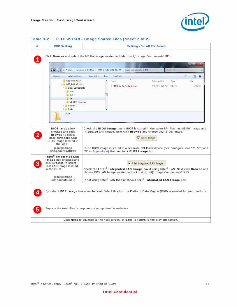
Intel® 7 Series Family - Intel® ME - 1.5MB FW Bring Up Guide 56
Intel Confidential
Image Creation: Flash Image Tool Wizard
Click Browse and select the ME FW image located in folder [root]\Image Components\ME \
BIOS Image box checked and click Browse to select
desktop/mobile CRB BIOS Image located in
the kit at:[root]\Image
Components\BIOS\
Check the BIOS Image box if BIOS is stored in the same SPI Flash as ME FW Image and Integrated LAN Image. Next click Browse and choose your BIOS image.
If the BIOS image is stored in a separate SPI Flash device (see Configurations “B”, “C”, and “D” in Appendix A) then uncheck BIOS Image box.
Intel® Integrated LAN Image box checked and click Browse to select CRB LAN Image located in the kit at:
[root]\Image Components\GbE\
Check the Intel® Integrated LAN Image box if using Intel® LAN. Next click Browse and choose CRB LAN Image located in the kit at: [root]\Image Components\GbE\
If not using Intel® LAN then uncheck Intel® Integrated LAN Image box.
By default PDR Image box is unchecked. Select this box if a Platform Data Region (PDR) is needed for your platform.
Reports the total Flash component size, updated in real-time
Click Next to advance to the next screen, or Back to return to the previous screen.
Table 3-2. FITC Wizard - Image Source Files (Sheet 2 of 2)
# CRB Setting Settings for All Platforms
1
2
3
4
5

Intel® 7 Series Family - Intel® ME - 1.5MB FW Bring Up Guide 57
Intel Confidential
Image Creation: Flash Image Tool Wizard
Table 3-3. FITC Wizard - VSCC Configuration
# CRB Setting Settings for All Platforms
Intel® CRBs use Flash devices W25Q64BV or AT26DF321. If the Flash device used on your platform is listed here, then click Next at the bottom of the screen to proceed. Otherwise, continue onto Step 2 to add your Flash device information.
Entry Name: W25Q64BVVendor ID: 0xEFDevice ID 0: 0x40Device ID 1: 0x17ME VSCC Value: 0x20052005
Using your SPI Flash device datasheet and Intel® 7 Series/C216 Chipset Family SPI Flash Programming Guide, enter the values for each field.
Click Add Entry button to add this Flash device to the list.
Flash device information can be updated by first selecting the Flash device from the list and then clicking the Edit Entry button.
Click Next to advance to the next screen, or Back to return to the previous screen.
1
2
3
4
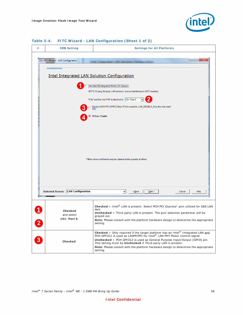
Intel® 7 Series Family - Intel® ME - 1.5MB FW Bring Up Guide 58
Intel Confidential
Image Creation: Flash Image Tool Wizard
Table 3-4. FITC Wizard - LAN Configuration (Sheet 1 of 2)
# CRB Setting Settings for All Platforms
Checked and select
101: Port 6
Checked = Intel® LAN is present. Select PCH PCI Express* port utilized for GbE LAN PHY. Unchecked = Third-party LAN is present. The port selection parameter will be grayed out.Note: Please consult with the platform hardware design to determine the appropriate setting.
Checked
Checked = Only required if the target platform has an Intel® Integrated LAN and PCH GPIO12 is used as LANPHYPC for Intel® LAN PHY Power Control signal.Unchecked = PCH GPIO12 is used as General Purpose Input/Output (GPIO) pin. This setting must be Unchecked if Third-party LAN is present.Note: Please consult with the platform hardware design to determine the appropriate setting.
1
2
3
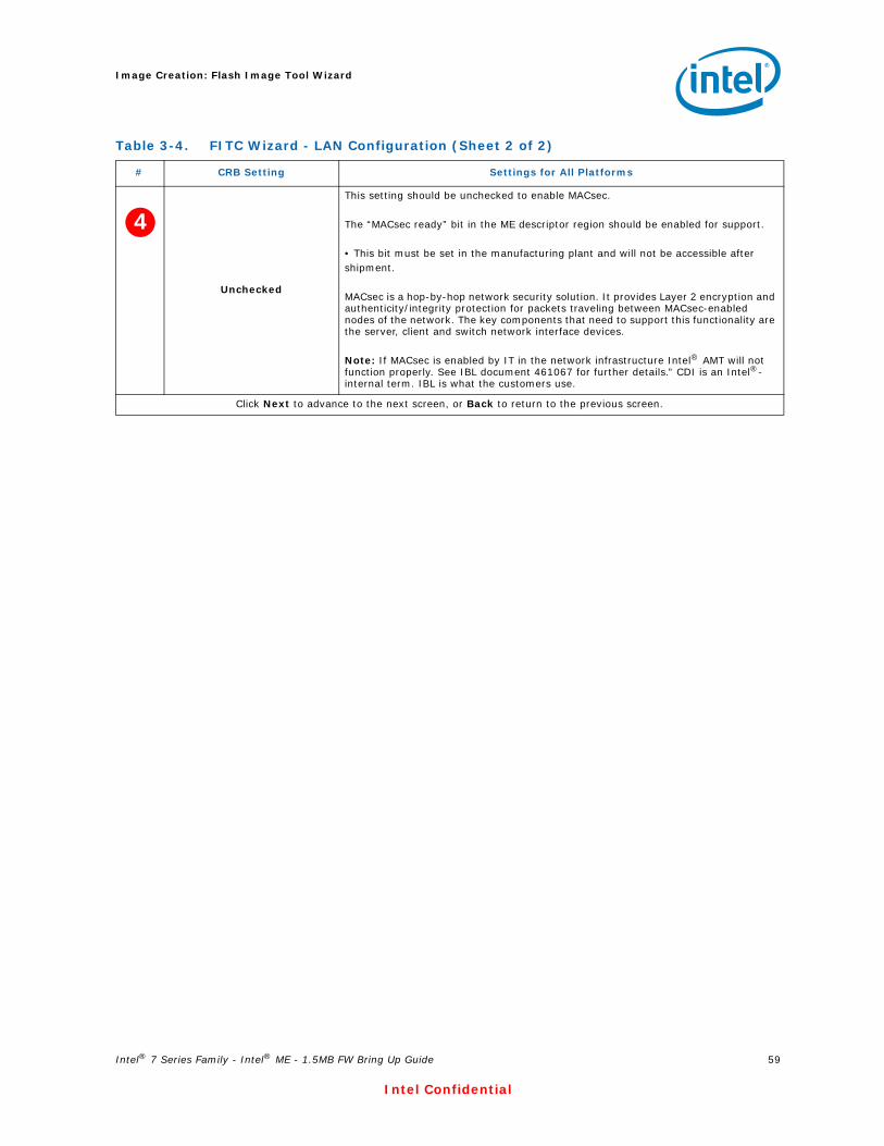
Intel® 7 Series Family - Intel® ME - 1.5MB FW Bring Up Guide 59
Intel Confidential
Image Creation: Flash Image Tool Wizard
Unchecked
This setting should be unchecked to enable MACsec.
The “MACsec ready” bit in the ME descriptor region should be enabled for support.
• This bit must be set in the manufacturing plant and will not be accessible aftershipment.
MACsec is a hop-by-hop network security solution. It provides Layer 2 encryption and authenticity/integrity protection for packets traveling between MACsec-enabled nodes of the network. The key components that need to support this functionality are the server, client and switch network interface devices.
Note: If MACsec is enabled by IT in the network infrastructure Intel® AMT will not function properly. See IBL document 461067 for further details.” CDI is an Intel®-internal term. IBL is what the customers use.
Click Next to advance to the next screen, or Back to return to the previous screen.
Table 3-4. FITC Wizard - LAN Configuration (Sheet 2 of 2)
# CRB Setting Settings for All Platforms
4

Intel® 7 Series Family - Intel® ME - 1.5MB FW Bring Up Guide 60
Intel Confidential
Image Creation: Flash Image Tool Wizard
Table 3-5. FITC Wizard - Intel® ME Application Permanent Disable (Sheet 1 of 2)
# CRB Setting Settings for All Platforms
Select the Platform Type that you wish to emulate on pre-production silicon. Valid Choices are:
• Intel® 7 Series Chipset• Intel® 6 Series Chipset
Select the Platform TypeSKU type that you wish to emulate on pre-production silicon. Valid Choices for Intel® 7 Series Chipset Platform are:
• Intel® Z77 Express Chipset• Intel® Z75 Express Chipset• Intel® H77 Express Chipset• Intel® H71 Express Chipset• Mobile Intel® HM70Express Chipset• Mobile Intel® HM76 Express Chipset• Mobile Intel® HM75 Express Chipset• Mobile Intel® UM77 Express Chipset• Mobile Intel® QS77 Express Chipset• Mobile Intel® HM77 Express Chipset
1
2

Intel® 7 Series Family - Intel® ME - 1.5MB FW Bring Up Guide 61
Intel Confidential
Image Creation: Flash Image Tool Wizard
Select the Platform Type SKU from the drop-down on pre-production silicon. Valid Choices for Intel® 6 Series Chipset Platform are:
•• Intel® H67 Express Chipset• Intel® P67 Express Chipset• Intel® H61 Express Chipset• Intel® Z68 Express Chipset• Mobile Intel® HM65 Express Chipset
Grayed out
The Manageability Application feature is not supported on 1.5MB FW SKUs and is grayed out
The 'KVM Permanently Disable' checkbox will disable the KVM system when selected.
Unchecked Intel® ME Network Services. If Permanently Disable is checked this will disable all ME Network Services communication except ARP offload and RMCP ping response.
Unchecked
If using Intel® integrated graphics solution and the target platform supports HD playback support from the Intel® Graphics driver, then PAVP must NOT be Disabled. Availability of PAVP feature is dependent on the SKU Type selected in Step 1. If this feature is not grayed out, then you have the option to permanently disable it by checking this box.
Unchecked
Checked = disables the Intel® Anti-Theft Technology (Intel® AT) feature.Unchecked = enables the Intel® Anti-Theft Technology (Intel® AT) feature. Note: Availability of Intel® AT feature is dependent on the SKU type selected in Step 2.
Click Next to advance to the next screen, or Back to return to the previous screen.
Table 3-5. FITC Wizard - Intel® ME Application Permanent Disable (Sheet 2 of 2)
# CRB Setting Settings for All Platforms
2
3
4
5
6

Intel® 7 Series Family - Intel® ME - 1.5MB FW Bring Up Guide 62
Intel Confidential
Image Creation: Flash Image Tool Wizard
Table 3-6. FITC Wizard - Intel® ME Kernel Configuration Parameters (Sheet 1 of 2)
# CRB Setting Settings for All Platforms
No Emulation
Set this parameter to the type of processor that the target system will use during production. This field will emulate that processor class for pre-production silicon. It is necessary to set this to 'EMULATE Intel® vPro (TM) capable Processor' in order to enable Intel® AMT feature support on pre-production CPUs
No onboard glue logic
This value will determine if glue logic is present on a Desktop platform to detect a missing processor. Choices are:• No onboard glue logic• Glue logic tied to GPIO24
Note: Please consult with the platform hardware design to determine the appropriate setting.
Checked
This option is to allow host access to the ME region during manufacturing/debug environments. See HMRFPO Intel® MEI Message Support in Intel® 7 Series/C216 Chipset Family ME BIOS Writers Guide for more details. Note: This setting is dependent on BIOS implementation. Please consult with the target platform’s BIOS vendor to determine the appropriate setting.
UncheckedThis enables Intel®ME M3 auto test during platform early boot.
1
2
3
4

Intel® 7 Series Family - Intel® ME - 1.5MB FW Bring Up Guide 63
Intel Confidential
Image Creation: Flash Image Tool Wizard
Grayed out Intel®Intel®Please consult with the platform hardware design to determine the appropriate settingPower Package 2: not supported for 1.5MB SKU
Checked
This value will determine if M3 power rail is present on the platform for proper firmware behaviorChecked = Platform hardware supports M3 power railUnchecked = Platform hardware has no separate M3 power railNote: Please consult with the platform hardware design to determine the appropriate setting.Note: This value is automatically checked and greyed out if Power Package 2 Supported is checked.
Unchecked
Checked = Platform HW configuration supports DSW rail and entry into Deep Sx.Unchecked = For mobile platforms, platform EC supports SUSPWRDNACK capability. For desktop platforms, platform does not support DSW rail or Deep Sx.Note: Please consult with the platform hardware design to determine the appropriate setting.
SLP_LAN# (MGPIO3)
This informs the Intel®ME how the Intel®LAN well is powered. If the target platform is NOT using Intel® LAN then set this to Core Well. Choices for LAN Power Well Config are:• Core Well• Sus Well• ME Well• SLP_LAN#
Note: Please consult with the platform hardware design to determine the appropriate setting.
Disabled
This informs Intel® ME how the Intel® WLAN is powered. If the target platform is NOT using WLAN for Manageability (Intel® AMT) then set this to Disabled. Choices for WLAN Power Well Config are:• Disabled (Default)• Sus Well• ME Well• Controlled via SLP_M# || SLP_ME_CSW_DEV#
Note: Please consult with the platform hardware design to determine the appropriatesetting.
FW Update OEM ID 00000000-0000-0000-0000-
000000000000FW Update OEM ID This field provides the ability to target FWUpdate (FWUpdLcl.exe) by Platform OEM. This ID will make sure that customers can only update a platform with an image coming from the platform OEM. If set to all zeros, then any input is valid when doing a firmware update.
Click Next to advance to the next screen, or Back to return to the previous screen.
Table 3-6. FITC Wizard - Intel® ME Kernel Configuration Parameters (Sheet 2 of 2)
# CRB Setting Settings for All Platforms
5
6
7
8
9
10

Intel® 7 Series Family - Intel® ME - 1.5MB FW Bring Up Guide 64
Intel Confidential
Image Creation: Flash Image Tool Wizard
Table 3-7.
# CRB Setting Settings for All Platforms
Default
Configures the Manageability Engine Redirection ports:Default - Enables all ports with no User Consent required for Redirection . (Security Level Low)Enhanced - Requires User Consent for Redirection . (Security Level Medium)Extreme - Disables Redirection (Security Level High)
Checked
Checked = Enables KVM to use keyboard and mouse input on USB ports connectedto EHCI 1Unchecked = Disables KVM to use keyboard and mouse input on USB portsconnected to EHCI 1
Unchecked
Checked = Enables KVM to use keyboard and mouse input on USB ports connected to EHCI 2Unchecked = Disables KVM to use keyboard and mouse input on USB ports connected to EHCI 2
Click Next to advance to the next screen, or Back to return to the previous screen.
1
2
3
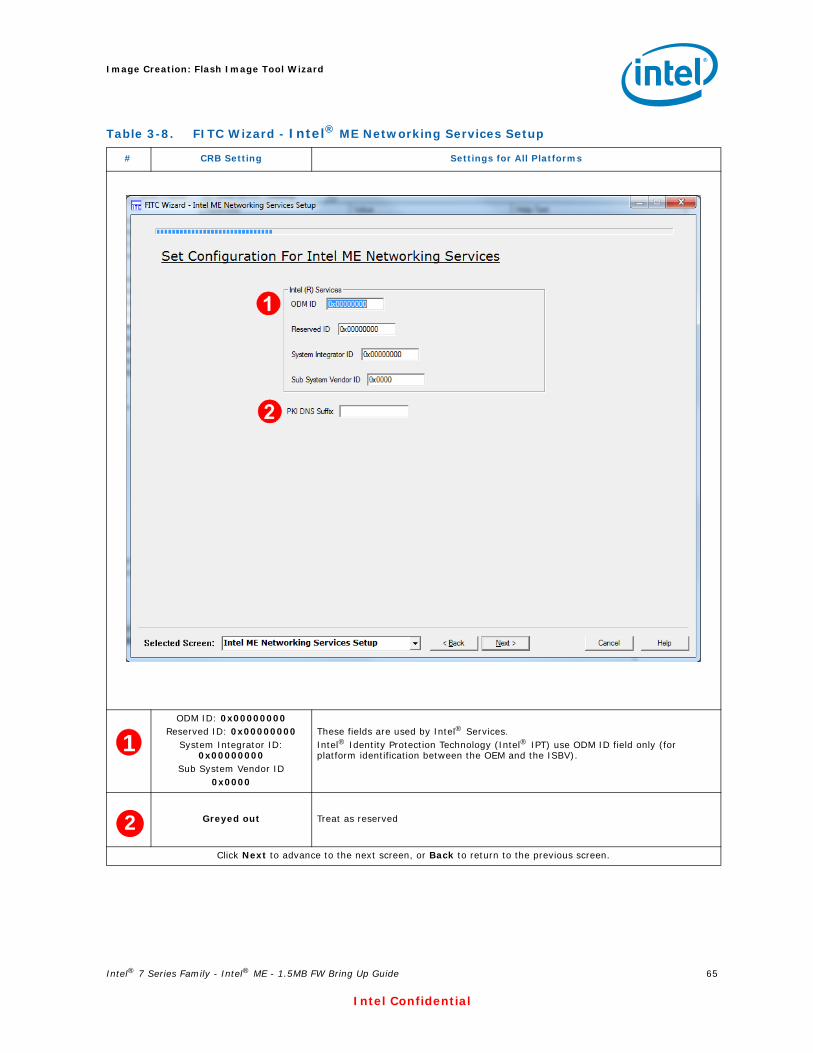
Intel® 7 Series Family - Intel® ME - 1.5MB FW Bring Up Guide 65
Intel Confidential
Image Creation: Flash Image Tool Wizard
Table 3-8. FITC Wizard - Intel® ME Networking Services Setup
# CRB Setting Settings for All Platforms
ODM ID: 0x00000000Reserved ID: 0x00000000
System Integrator ID: 0x00000000
Sub System Vendor ID0x0000
These fields are used by Intel® Services. Intel® Identity Protection Technology (Intel® IPT) use ODM ID field only (for platform identification between the OEM and the ISBV).
Greyed out Treat as reserved
Click Next to advance to the next screen, or Back to return to the previous screen.
1
2
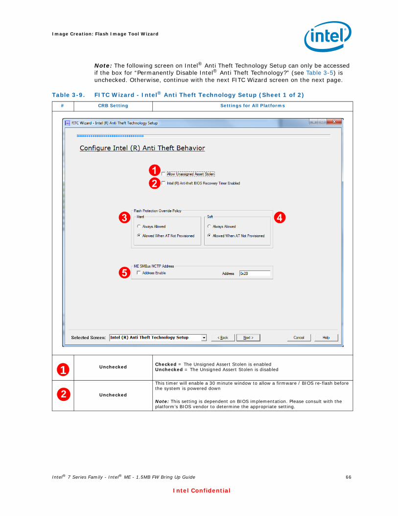
Intel® 7 Series Family - Intel® ME - 1.5MB FW Bring Up Guide 66
Intel Confidential
Image Creation: Flash Image Tool Wizard
Note: The following screen on Intel® Anti Theft Technology Setup can only be accessed if the box for “Permanently Disable Intel® Anti Theft Technology?” (see Table 3-5) is unchecked. Otherwise, continue with the next FITC Wizard screen on the next page.
Table 3-9. FITC Wizard - Intel® Anti Theft Technology Setup (Sheet 1 of 2)
# CRB Setting Settings for All Platforms
Unchecked Checked = The Unsigned Assert Stolen is enabled Unchecked = The Unsigned Assert Stolen is disabled
Unchecked
This timer will enable a 30 minute window to allow a firmware / BIOS re-flash before the system is powered down
Note: This setting is dependent on BIOS implementation. Please consult with the platform’s BIOS vendor to determine the appropriate setting.
1
2
Intel® 7 Series Family - Intel® ME - 1.5MB FW Bring Up Guide 67
Intel Confidential
Image Creation: Flash Image Tool Wizard
Allowed When AT Not Provisioned
This option determines if the Intel®ME will enter a disabled state to allow full SPI device re-flashing when the manufacturing override jumper (HMFPRO) is set.
Always Allowed - Full SPI re-flash will always be allowed regardless of AT enrollment state.
Allowed When AT Not Provisioned - Full SPI re-flash allowed if AT has not been enrolled.
Allowed When AT Not Provisioned
This option determines if the Intel®ME will enter a disabled state via BIOS based MEI messages and allow Intel®ME only region re-flash.
Always Allowed - Intel®ME region re-flash will always be allowed regardless of AT enrollment state.
Allowed When AT Not Provisioned - Intel®ME region re-flash allowed if AT has not been enrolled.
Address Enable unchecked
Address 0x2B
This setting is for 3G NIC support for Intel® AT. If this card is supported by the target platform, then select Address enable and set the SMBus address for the card.
Note: Please consult with the platform hardware design to determine the appropriate setting.
Click Next to advance to the next screen, or Back to return to the previous screen.
Table 3-9. FITC Wizard - Intel® Anti Theft Technology Setup (Sheet 2 of 2)
# CRB Setting Settings for All Platforms
3
4
5
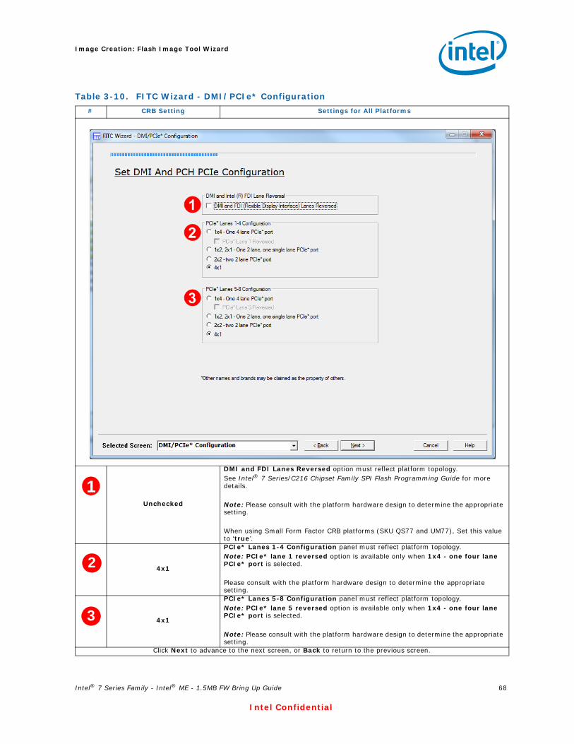
Intel® 7 Series Family - Intel® ME - 1.5MB FW Bring Up Guide 68
Intel Confidential
Image Creation: Flash Image Tool Wizard
Table 3-10. FITC Wizard - DMI/PCIe* Configuration # CRB Setting Settings for All Platforms
Unchecked
DMI and FDI Lanes Reversed option must reflect platform topology.See Intel® 7 Series/C216 Chipset Family SPI Flash Programming Guide for more details.
Note: Please consult with the platform hardware design to determine the appropriate setting.
When using Small Form Factor CRB platforms (SKU QS77 and UM77), Set this value to ‘true’.
4x1
PCIe* Lanes 1-4 Configuration panel must reflect platform topology.Note: PCIe* lane 1 reversed option is available only when 1x4 - one four lane PCIe* port is selected.
Please consult with the platform hardware design to determine the appropriate setting.
4x1
PCIe* Lanes 5-8 Configuration panel must reflect platform topology.Note: PCIe* lane 5 reversed option is available only when 1x4 - one four lane PCIe* port is selected.
Note: Please consult with the platform hardware design to determine the appropriate setting.
Click Next to advance to the next screen, or Back to return to the previous screen.
1
2
3

Intel® 7 Series Family - Intel® ME - 1.5MB FW Bring Up Guide 69
Intel Confidential
Image Creation: Flash Image Tool Wizard
Table 3-11. FITC Wizard - Thermal Reporting (Sheet 1 of 2)
# CRB Setting Settings for All Platforms
Checked for CRB
Checked =Check this for EC/SIO/BMC to interact Thermal Reporting feature over SMLink1Unchecked = Platform has no EC/SIO/BMC on SMLink1
Note: Please consult with the target hardware designer to determine this setting.
CRB uses 0x4C
Denotes EC/SIO/BMC SMBus write address over SMLink1.
For mobile platforms, this field cannot be blank, otherwise the Next button will be disabled.
Note: Please consult with the platform hardware design to determine the appropriate setting.
CRB uses 0x4B
Denotes EC/SIO/BMC SMBus read address over SMLink1.
For mobile platforms, this field cannot be blank, otherwise the Next button will be disabled.
Note: Please consult with the target hardware designer to determine this setting.
1
2
3

Intel® 7 Series Family - Intel® ME - 1.5MB FW Bring Up Guide 70
Intel Confidential
Image Creation: Flash Image Tool Wizard
Desktop - CPU, PCH, & DIMMS
Mobile - PCH Only
Select between thermal reporting using:• CPU, PCH, & DIMMS: Legacy Intel®ME FW SMBus based thermal reporting that
reports Processor, PCH and DIMMs
Note: ME Thermal Reporting: Advantage = Does not require PECI capability in EC. Disadvantage = no real time temperature alert level control, and no dynamic Sandy Bridge or Ivy Bridge CPU Turbo controls.
— PECI from Sandy Bridge processor is connected to PCH— BIOS sets Thermal Reporting Control (TRC) MMIO register at TBARB+1Ah
to enable ME reporting of processor, PCH, and DIMM temperatures (as appropriate)
— Intel®ME thermal reporting PCI device should be enabled for proper interaction with EC, SIO, BMC, or equivalent fan control logic
• PCH Only: HW based PCH only thermal reporting. This would require PECI to be hooked up directly to EC/SIO in order to get processor temperature
Note: Platform based Thermal Reporting: Advantage = allows full dynamic Sandy Bridge / Ivy Bridge Turbo control. Disadvantage = Requires EC/BMC with PECI capability.
— PECI from Sandy Bridge processor is connected direct to EC, SIO, BMC, or equivalent fan control logic
— BIOS sets Thermal Reporting Control (TRC) MMIO register at TBARB+1Ah = 0x0, disabling Intel®ME reporting of processor, PCH, and DIMM temperatures
— Intel®ME thermal reporting PCI device should be disabled
Click Next to advance to the next screen, or Back to return to the previous screen.
Table 3-11. FITC Wizard - Thermal Reporting (Sheet 2 of 2)
# CRB Setting Settings for All Platforms
4

Intel® 7 Series Family - Intel® ME - 1.5MB FW Bring Up Guide 71
Intel Confidential
Image Creation: Flash Image Tool Wizard
Table 3-12. FITC Wizard - Boot Configuration Options (Sheet 1 of 2)
# CRB Setting Settings for All Platforms
64 KB
BIOS Boot Block Size is the bare minimum BIOS code required to boot a platform. This setting allows for proper address bit to be inverted as required by BIOS Boot Block Size.
64KB = Invert A16 if Top Swap is enabled128KB = Invert A17 if Top Swap is enabled256KB = Invert A18 if Top Swap is enabled
If BIOS is stored in a separate SPI Flash device (see Appendix A for details about Configurations “B”, “C”, and “D”) then leave this parameter at 64KB.
Note: This field will be disabled when BIOS Image (see Table 3-2) is not checked.
Note: This must be determined by the target platform BIOS developer.
1

Intel® 7 Series Family - Intel® ME - 1.5MB FW Bring Up Guide 72
Intel Confidential
Image Creation: Flash Image Tool Wizard
Unchecked
Indicates if RequesterID checking during DMI accesses is disabled. This parameter is only applicable for server platforms that contain multiple Processors.
Unchecked = single Processor in the same platform
Checked = multiple Processors in the same platform
Note: Please consult with the platform hardware design to determine the appropriate setting.
Click Next to advance to the next screen, or Back to return to the previous screen.
Table 3-12. FITC Wizard - Boot Configuration Options (Sheet 2 of 2)
# CRB Setting Settings for All Platforms
2

Intel® 7 Series Family - Intel® ME - 1.5MB FW Bring Up Guide 73
Intel Confidential
Image Creation: Flash Image Tool Wizard
Table 3-13. FITC Wizard - Integrated Clock Configuration
# CRB Setting Settings for All Platforms
# CRB Setting Settings for All Platforms
1
SPI flash binary images across multiple board designs can contain the same block of Clock Control Parameters (OEM Request Records), up to 7 sets total.This parameter selects how many total OEM Request Records will be built into the image.Note: The next 2 screens will be repeated for as many OEM Request Records that will be present.
Soft Strap
If more than one OEM Request Record is present in SPI, then this parameter specifies whether Soft Strap or BIOS determines the ICC Boot Profile. Note that the BIOS option has additional BIOS requirements, see BIOS Writers Guide for more details. These requirements include:• Details on the Intel® MEI message BIOS can use to read or specify ICC Boot Profile• Details on reset requirements after BIOS has specified an ICC Boot Profile
0
Specifies which clock control parameter set is to be used by the final generated SPI flash binary image by the target platform at boot time. This parameter is only used if ICC Boot Profile is specified by Soft Strap. If BIOS is specifying ICC Boot Profile, then this parameter is unused.
Click Next to advance to the next screen, or Back to return to the previous screen.
1
2
3

Intel® 7 Series Family - Intel® ME - 1.5MB FW Bring Up Guide 74
Intel Confidential
Image Creation: Flash Image Tool Wizard
Table 3-14. FITC Wizard - ICC Profile 0 Single-Ended Clocks (Sheet 1 of 2)
# CRB Setting Settings for All Platforms
Checked for all PCI and FLEX clocks
Unchecked = Output clock is gated to low state Checked = Output buffer is enabled to toggle once its clock source has been initialized
33.3 MHz for FLEX0, FLEX214.31818 MHz for FLEX1
24/48MHz for FLEX3
Controls muxing to select sources for FLEX clock outputs.Note: PCI clock outputs are fixed at 33 MHz, but FLEX clock outputs may be configured to act as PCI outputs.
Note: These clock select settings only take effect when this muxed FLEXCLK/GPIO pin is configured for FLEXCLK native usage. Refer to the Panther Peak EDS for configuration of GPIO vs. native usage.
Note: 27 Mhz option is available in the tool, but is not extensively tested by Intel®and is not recommended for use.
4-Default Slew Rate for all PCI and Flex clocks
Controls slew rate for PCI and FLEX clocks. PCI Specifications 2.4 and 3.0 allow for an acceptable slew rate range of 1 to 4 V/ns. ME FW programmability allows for slew rate to be specified between 0.6 to 2 V/ns for two reasons:• Slew rates exceeding 2 V/ns can have adverse effects on platform EMI• Slew rates lower than 1 V/ns can be specified for EMI benefits, at the risk of
violating PCI specification
1
2
3

Intel® 7 Series Family - Intel® ME - 1.5MB FW Bring Up Guide 75
Intel Confidential
Image Creation: Flash Image Tool Wizard
Double-loaded for all PCI and FLEX clocks
Sets programmable series resistance for PCI and FLEX clocks.
Unchecked for all PCI and FLEX clocks
Enables support for CLKRUN protocol for PCI 33 MHz clocks muxed out to CLKOUTFLEX[3:0] and CLKOUT_PCI[4:0].Unchecked = Corresponding CLKOUTFLEX PCI clock is free-running, unaffected by CLKRUN protocol Checked = Corresponding CLKOUTFLEX PCI clock is shut off when CLKRUN protocol turns off PCI clocksNote: When the corresponding CLKOUTFLEX pins are not configured for PCI 33Mhz clock, this option is disabled and unchecked.
Reports the dword values of FCSS, OCKEN, SEBP1, SEBP2, and PM2 Clock Control Parameters, as they are affected by the settings on this screen.See Appendix B for more information on Clock Control Parameters.
Click Next to advance to the next screen, or Back to return to the previous screen.
Table 3-14. FITC Wizard - ICC Profile 0 Single-Ended Clocks (Sheet 2 of 2)
# CRB Setting Settings for All Platforms
4
5
6

Intel® 7 Series Family - Intel® ME - 1.5MB FW Bring Up Guide 76
Intel Confidential
Image Creation: Flash Image Tool Wizard
Table 3-15. FITC Wizard - ICC Profile 0 Platform & Differential Clocks (Sheet 1 of 2)
# CRB Setting Settings for All Platforms
Checked for all differential clock outputs (PEG[B:A],
SRCITPXDP, SRC[7:0], DP120)
Unchecked = Output clock is gated to low state Checked = Output buffer is enabled to toggle once its clock source has been initialized
Disable dynamic control for all PCI Express* clocks (PEG[B:A], SRCITPXDP,
SRC[7:0])
Assigns dynamic CLKRQ# control of SRC clocks. Each PCI Express* clock may be assigned to a muxed CLKRQ#/GPIO PCH pin.Note: These CLKRQ# settings only take effect when this muxed CLKRQ#/GPIO pin is configured for CLKRQ# native usage. Refer to the Intel® 7 Series/C216 Chipset Family EDS for configuration of GPIO vs. native usage.
Full Clock Integration Mode - NO Overclocking
Full Clock Integration Mode - NO Overclocking = PCH natively generates all platform clocks. Platform will not utilize BCLK overclocking.Full Clock Integration Mode - YES Overclocking = PCH natively generates all platform clocks. Platform WILL utilize BCLK overclocking.Display Clock Integration= This is NOT an ICC mode that is supported by the Intel® 7 Series/C216 Chipset Family. This mode will not be validated by Intel® and should not be used in Intel® 7 Series/C216 Chipset Family.
1
2
3
Intel® 7 Series Family - Intel® ME - 1.5MB FW Bring Up Guide 77
Intel Confidential
Image Creation: Flash Image Tool Wizard
Integrated Only or Integrated & 27MHz
Discrete Graphics Down Device
External Graphics only = Use this setting if platform supports external graphics onlyIntegrated Only or Integrated & 27MHz Discrete Graphics Down Device = Display clock will be controlled by Intel® Integrated Graphics Device Driver and the Display Clock will only be supplied to the Intel® Integrated Graphics Device. Any Graphics Down Devices with 27-MHz clock requirement is required to utilize an external 27-MHz crystal since:• PCH cannot simultaneously supply 120 MHz Integrated Graphics clock and 27-
MHz Down Device clock simultaneously• Simultaneous clocking is required for both switchable and mixed graphics
configurationsDiscrete Graphics Down Device Only = This option is NOT supported in Intel® 7 Series/C216 Chipset Family
External Graphics only = Use this setting if platform supports external graphics only
Reports the dword values of OCKEN, CSS, PLLRCS, DIVEN, PMSRCCLK1, PMSRCCLK2, IBEN, SSS, SSCCTL, PI12BIASPARAMS, and PLLEN Clock Control Parameters, as they are affected by the settings on this screen.See Appendix B for more information on Clock Control Parameters.
Click Next to advance to the next screen, or Back to return to the previous screen.
Table 3-15. FITC Wizard - ICC Profile 0 Platform & Differential Clocks (Sheet 2 of 2)
# CRB Setting Settings for All Platforms
4
5

Intel® 7 Series Family - Intel® ME - 1.5MB FW Bring Up Guide 78
Intel Confidential
Image Creation: Flash Image Tool Wizard
Table 3-16. FITC Wizard - Production/Nonproduction Configuration (Sheet 1 of 2)
# CRB Setting Settings for All Platforms
Non-production mode
Selecting Production Mode sets the following:• BIOS Region Master Access Permissions set to 0x0B for read access and 0x0A for write
access• Intel®ME FW Region Master Access Permissions set to 0x0D for read access and 0x0C
for write access• GbE FW Region Master Access Permissions set to 0x08 for both read and write access• ME SMBus Diagnostic Console capability is disabled• MDDD capability is disabled
Selecting Non-production Mode sets the following:• Master Access Permissions for all SPI Flash Regions set to 0xFF for both read and write
access• Intel®ME SMBus Diagnostic Console capability is disabled• MDDD capability is disabled
Production Mode is for a system as it would be shipped. Non-production Mode is for debug and simplifies flashing new images onto SPI Flash.
Production Mode With BIOS Read/Write Access to PDR - This option functions the same as Production Mode with the addition of allowing BIOS Read and Write access to the Platform Data Region for the SPI flash.
1

Intel® 7 Series Family - Intel® ME - 1.5MB FW Bring Up Guide 79
Intel Confidential
Image Creation: Flash Image Tool Wizard
UncheckedFor mobile platforms only. When this field is checked, Intel®Management Engine will assert CL_RST1# when it resets. When set to unchecked, Intel®ME does not reflect this reset.
Unchecked Enabled Intel®ME Debug to operate in emergency mode. See Intel®ME Debug documentation for more detail.
Enabled: UncheckedAddress: 0x00
Note: This option should not be enabled. Treat as Reserved.
Click Next to advance to the next screen, or Back to return to the previous screen.
Table 3-16. FITC Wizard - Production/Nonproduction Configuration (Sheet 2 of 2)
# CRB Setting Settings for All Platforms
2
3
4

Intel® 7 Series Family - Intel® ME - 1.5MB FW Bring Up Guide 80
Intel Confidential
Image Creation: Flash Image Tool Wizard
Table 3-17. FITC Wizard - Build (Sheet 1 of 2)
# CRB Setting Settings for All Platforms
Specify filename and directory location of output image. By default, the filename used is outimage.bin and the location will be in the same directory as fitc.exe.1

Intel® 7 Series Family - Intel® ME - 1.5MB FW Bring Up Guide 81
Intel Confidential
Image Creation: Flash Image Tool Wizard
After clicking Build, the Flash image will be created and all setting will be present in FITC. If you want to save the setting, use File -> Save as, to save the settings in the xml specified.
Now that the 1.5MB5MB SPI Flash image has been created, you may jump to Section 4, “Programming SPI Flash Devices and Checking Firmware Status” .
Section 2, “Image Creation: Flash Image Tool (FITC)” is only intended
for advanced Flash image creation and most users will not need to follow it.
Click Build to create the SPI Flash image.
Note: In addition to the outimage.bin file created, there may be two extra output images created as well,• outimage(1).bin• outimage(2).bin
These two images are used for programming the SPI Flash devices separately (for example, using an external Flash programmer).
Note - Full Clock Integration Mode - NO Overclocking: You may experience a test fail result for Intel® Management Engine Test Suite (Intel® ME Test Suite) test ICC_TST_10, unless you set an additional value in FITC after finishing with Wizard. This means you will not Build an image after finishing the Wizard. Instructions:• In FITC (not Wizard mode) navigate to Flash Image | ME Region | Configuration | ICC Data | ICC Profile 0 |
Clock Range Definition Record 0 (or appropriate record #0-7)• Navigate to subfolder Clock Range Definition Record | Processor or Platform DMICLK (DIV2-S). You will be
changing a setting for the main PCI Express* clock divider• Change parameter Clock Div Min to 0xC00• Change parameter Clock Div Max to 0xC00 for basic configuration. If platform support Wimax friendly clocking,
set the value to 0xC0ENot taking the above steps has no risk or issue for production configuration and is meant to help platform successfully meet METS requirements for ICC_TST_11 only.
Click Finish to preserve all Wizard build settings and parameters and return to FITC advanced mode.
Click Next to advance to the next screen, or Back to return to the previous screen.
Table 3-17. FITC Wizard - Build (Sheet 2 of 2)
# CRB Setting Settings for All Platforms
2
3

Intel® 7 Series Family - Intel® ME - 1.5MB FW Bring Up Guide 53
Intel Confidential
Programming SPI Flash Devices and Checking Firmware Status
3 Programming SPI Flash Devices and Checking Firmware Status
Now that the Flash image file has been created, it can be programmed into the SPI Flash device(s) of the target machine. For platforms that don’t boot, a Flash Chip Programmer will be required. For platforms that can boot to DOS or Windows*, the Flash Programming Tool (FPT) can be used.
3.1 Flash Burner/ProgrammerThe specific use of a Flash burner/programmer is beyond the scope of this document. However, the following general steps may be followed:
1. Navigate to your Output Directory (as specified in Section 3.2 or Section 2.6.2) where your generated SPI Flash image(s) are saved. It is assumed that this image file is named outimage.bin. If two total SPI Flash devices were specified during the build process, then additional image files will be saved, one for each SPI Flash device. These files are assumed to be named outimage(1).bin and outimage(2).bin.
2. Utilize a Flash burner/programmer to program the image(s). For multiple SPI Flash devices, the images are numbered sequentially to correspond to the first and second SPI Flash device accordingly.
3.1.1 In-Circuit SPI Flash Programming for Mobile CRBMobile CRBs have the SPI Flash devices soldered down. As a result, to program the SPI Flash for mobile CRBs, follow these steps:
1. Leave mobile CRB powered off.2. Connect Flash Programmer (such as DediProg SF100) header to connector J8E1
which is labelled “SPI PROG”. Make sure to line up pin 1 on the header.
3. Change the jumpers to the “Programming SPI-0” mode as shown in Table 4-1 below.
4. Program the first image [outimage(1).bin] to the CRB.
5. Following Table 4-1, change the jumpers to the “Programming SPI-1” mode.
6. Program the second image [outimage(2).bin] to the CRB.
7. Once programming is complete, disconnect the Flash Programmer header. The CRB is now ready for power on.
Table 3-1. Jumper Settings for Mobile CRB SPI Flash Programming
Mode J8C4 J8C5 J8D1
Programming SPI-0 1-2 1-2 1-2
Programming SPI-1 1-2 1-2 2-3
Normal Operation 1-X 1-X 1-X

Intel® 7 Series Family - Intel® ME - 1.5MB FW Bring Up Guide 54
Intel Confidential
Programming SPI Flash Devices and Checking Firmware Status
3.2 Flash Programming Tool (FPT)FPT can be used to substitute for a Flash burner/programmer, provided the system is capable of booting to a DOS or Windows OS.
Note: FPT will automatically disable the Intel® ME prior to flashing the image to the platform.
FPT DOS Version
The DOS versions supported by FPT are: DOS, Free DOS, and DRMK DOS. Use the following steps to program the SPI Flash devices,
1. Copy all the files in the “(root)\Tools\System Tools\Flash Programming Tool\DOS” directory to the root directory of a bootable USB key.
2. Navigate to your Output Directory (as specified in Section 3.2 or Section 2.6.2) where your generated SPI Flash image(s) are saved. It is assumed that this image file is named outimage.bin. Copy this image file to the root directory of the USB key.
3. Boot the target system to DOS and change to the root directory of the bootable USB key. At the DOS prompt type:
The system should respond with the number of SPI Flash devices available. For example:
Note: If the SPI Flash device does not currently contain a descriptor it may report only a single device.
4. Program the SPI Flash image to the Flash device(s) by issuing the following command at the prompt:
If the programming was successful, then the following message will be shown.
If the programming was NOT successful, then repeat this step to try again. If programming problems persist, then check the SPI Flash devices and platform hardware.
5. Execute a platform global reset using FPT -greset. Next go to Section 3.3 to check the Intel® ME Firmware status.
fpt.exe /i
--- Flash Devices Found --- W25Q64BV ID:0xEF4017 Size: 8192KB (65536Kb) W25Q64BV ID:0xEF4017 Size: 8192KB (65536Kb)
fpt.exe /f outimage.bin
FPT Operation Passed

Intel® 7 Series Family - Intel® ME - 1.5MB FW Bring Up Guide 55
Intel Confidential
Programming SPI Flash Devices and Checking Firmware Status
3.2.1 FPT Windows* VersionThe Windows* OS versions supported by FPT are: Windows* PE, Windows* XP SP2, Windows* Vista and Windows* 7. There are two versions of FPT for Windows*: a 32-bit version and a 64-bit version. Most Windows* OS, Windows* XP, Vista, Windows* 7 (32-bit or 64-bit) and Windows* 8 (32-bit or 64-bit) can use Windows* version of FPT. However, Windows* OS which do not support 32 bit compatible mode (Win PE 64-bit) must use FPT Windows* 64-bit version due to compatibility issues.
Use the following steps to program the SPI Flash devices,
1. Navigate to your Output Directory (as specified in Section 3.2 or Section 2.6.2) where your generated SPI Flash image(s) are saved. It is assumed that this image file is named outimage.bin. Copy this image file to FPT directory located at “(root) \Tools\System Tools\Flash Programming Tool\Windows”.
2. Boot the target system to Windows* and open a Command Prompt window. In this window, change to the FPT directory and at the prompt type:
The system should respond with the number of SPI Flash devices available. For example:
Note: If the SPI Flash device does not currently contain a descriptor it may report only a single device.
3. Program the SPI Flash image to the Flash device(s) by issuing the following command at the prompt:
If the programming was successful, then the following message will be shown.
If the programming was NOT successful, then repeat this step to try again. If programming problems persist, then check the SPI Flash devices and platform hardware.
4. Power down the platform with a G3 power cycle (ensure all power is disconnected from the system). Next go to Section 3.3 to check the Intel® ME Firmware status.
3.3 Checking Intel® ME Firmware StatusUse the following steps to check the platform health and Intel® ME FW status,
1. Copy the file MEInfo.exe in the “(root)\Tools\System Tools\MEInfo\DOS” directory to the root directory of a bootable USB key.
fptw.exe /i
--- Flash Devices Found --- W25Q64BV ID:0xEF4017 Size: 8192KB (65536Kb) W25Q64BV ID:0xEF4017 Size: 8192KB (65536Kb)
fptw.exe /f outimage.bin
FPT Operation Passed

Intel® 7 Series Family - Intel® ME - 1.5MB FW Bring Up Guide 56
Intel Confidential
Programming SPI Flash Devices and Checking Firmware Status
2. Boot the target system and stop at the BIOS setup menu. Load default values for BIOS (on Intel® CRBs press F3 to load default values). Save and reboot (on Intel® CRBs press F4 and select Yes).
3. Boot the target system to DOS and change to the root directory of the bootable USB key. At the DOS prompt type:
The system should respond with a message similar to below.
As in the above example if there are NO errors shown, then• your platform’s health is good• Intel® ME FW has successfully initialized• Intel® ME FW is operating normally
Note: This section is only intended to show how to use the MEInfo.exe tool for checking firmware status. For full usage and capabilities of the MEInfo.exe tool, please see the System Tools User Guide.
MEInfo.exe
Intel(R) MEInfo Version: 8.1.0.xxxxCopyright(C) 2005 - 2011, Intel Corporation. All rights reserved.
Intel(R) Manageability and Security Application code versions:
BIOS Version: ACRVMBY1.86C.0035.B00.1103131018MEBx Version: 8.1.0.xxGbe Version: 1.3VendorID: 8086PCH Version: 600000FW Version: 8.1.0.xxxx
FW Capabilities: 0x0DFE5C67
Intel(R) Active Management Technology - PRESENT/ENABLED Intel(R) Anti-Theft Technology - PRESENT/ENABLED Intel(R) Capability Licensing Service - PRESENT/ENABLED Protect Audio Video Path - PRESENT/ENABLED Intel(R) ME Dynamic Application Loader - PRESENT/ENABLED
Intel(R) AMT State: EnabledCPU Upgrade State: Upgrade CapableCryptography Support: EnabledLast ME reset reason: Power upLocal FWUpdate: EnabledBIOS and GbE Config Lock: EnabledHost Read Access to ME: EnabledHost Write Access to ME: EnabledSPI Flash ID #1: EF4017SPI Flash ID VSCC #1: 20052005BIOS boot State: Post BootOEM Id: 00000000-0000-0000-0000-000000000000

Intel® 7 Series Family - Intel® ME - 1.5MB FW Bring Up Guide 57
Intel Confidential
Programming SPI Flash Devices and Checking Firmware Status
3.4 Common Bring Up Issues and Troubleshooting Table
§ §
Table 3-2. Common Bring Up Issues and Troubleshooting Table
Problem / Issue Solution / Workaround
System does not boot to DOS
By default, the system will boot to EFI Shell. To boot to DOS,1. Enter BIOS menu, then go to the ‘Boot’ screen2. Change ‘Boot Option #1’ to be your USB key (ensure USB key is
formatted to be DOS bootable)3. Press ‘F4’ to save settings and reboot
Hear 3 beeps when platform powers on
Possible device is disconnected or device not found, check• platform power and CPU fan power connectors• DIMM memory modules• USB devices (keyboard, mouse, USB key) may be plugged into
inactive USB port• missing/incorrect jumpers• missing CPU or PCH
No display on monitor Ensure 1.5MB FW SKU supports integrated graphics. Try external graphics card.
USB device not detected or does not work
USB device may be plugged into inactive USB port
System does not boot (Post Code 00)
Incorrect Flash image – possible reasons: • wrong FW selected during Flash image build process• wrong Flash size selected
Re-build image with correct settings and re-flash using Flash burner.

Intel® 7 Series Family- Intel® ME - 1.5MB FW Bring Up Guide 58
Intel Confidential
Intel® ME Firmware Features - Details and Settings
4 Intel® ME Firmware Features - Details and Settings
All parameters in this section are color-coded as per the key below.
The parameter can be changed
The parameter is read only and cannot be changed
Table 4-1. Feature Default Settings by 7 Series SKU (Desktop) (Sheet 1 of 2)
7 Series Feature Default Value
Intel® H77 - Desktop Enable Intel® Standard Manageability; Disable Intel® AMT Yes
Managability Application Permanently Disabled? No
PAVP Permanently Disabled? No
TLS Permanently Disabled? No
Intel® Anti-Theft Technology Permanently Disabled? No
Intel® ME Network Services Permanently Disabled? No
mDNS Proxy Permanently Disabled? Yes
Intel® Manageability Application Enable / Disable Enabled
Intel® Z77 - Desktop Enable Intel® Standard Manageability; Disable Intel® AMT Yes
Managability Application Permanently Disabled? Yes
PAVP Permanently Disabled? No
TLS Permanently Disabled? Yes
Intel® Anti-Theft Technology Permanently Disabled? No
Intel® ME Network Services Permanently Disabled? No
mDNS Proxy Permanently Disabled? Yes
Intel® Manageability Application Enable / Disable Disabled
Intel® Z75 - Desktop Enable Intel® Standard Manageability; Disable Intel® AMT Yes
Managability Application Permanently Disabled? Yes
PAVP Permanently Disabled? No
TLS Permanently Disabled? Yes
Intel® Anti-Theft Technology Permanently Disabled? No
Intel® ME Network Services Permanently Disabled? No
mDNS Proxy Permanently Disabled? Yes
Intel® Manageability Application Enable / Disable Disabled

Intel® 7 Series Family- Intel® ME - 1.5MB FW Bring Up Guide 59
Intel Confidential
Intel® ME Firmware Features - Details and Settings
Intel® H71 - Desktop Enable Intel® Standard Manageability; Disable Intel® AMT Yes
Managability Application Permanently Disabled? Yes
PAVP Permanently Disabled? No
TLS Permanently Disabled? Yes
Intel® Anti-Theft Technology Permanently Disabled? No
Intel® ME Network Services Permanently Disabled? No
mDNS Proxy Permanently Disabled? Yes
Intel® Manageability Application Enable / Disable Disabled
Table 4-1. Feature Default Settings by 7 Series SKU (Desktop) (Sheet 2 of 2)
7 Series Feature Default Value

Intel® 7 Series Family- Intel® ME - 1.5MB FW Bring Up Guide 60
Intel Confidential
Intel® ME Firmware Features - Details and Settings
All parameters in this section are color-coded as per the key below.
The parameter can be changed
The parameter is read only and cannot be changed
Table 4-2. Feature Default Settings by 6 Series SKU (Desktop)
6 Series Feature Default Value
Intel® H67 - Desktop Enable Intel® Standard Manageability; Disable Intel® AMT Yes
Managability Application Permanently Disabled? No
PAVP Permanently Disabled? No
TLS Permanently Disabled? No
Intel® Anti-Theft Technology Permanently Disabled? Yes
Intel® ME Network Services Permanently Disabled? No
mDNS Proxy Permanently Disabled? Yes
Intel® Manageability Application Enable / Disable Enabled
Intel® Z68 - Desktop Enable Intel® Standard Manageability; Disable Intel® AMT Yes
Managability Application Permanently Disabled? Yes
PAVP Permanently Disabled? No
TLS Permanently Disabled? Yes
Intel® Anti-Theft Technology Permanently Disabled? Yes
Intel® ME Network Services Permanently Disabled? No
mDNS Proxy Permanently Disabled? Yes
Intel® Manageability Application Enable / Disable Disabled
Intel® P67 - Desktop Enable Intel® Standard Manageability; Disable Intel® AMT Yes
Managability Application Permanently Disabled? Yes
PAVP Permanently Disabled? Yes
TLS Permanently Disabled? Yes
Intel® Anti-Theft Technology Permanently Disabled? Yes
Intel® ME Network Services Permanently Disabled? No
mDNS Proxy Permanently Disabled? Yes
Intel® Manageability Application Enable / Disable Disabled
Intel® H61 - Desktop Enable Intel® Standard Manageability; Disable Intel® AMT Yes
Managability Application Permanently Disabled? Yes
PAVP Permanently Disabled? No
TLS Permanently Disabled? Yes
Intel® Anti-Theft Technology Permanently Disabled? Yes
Intel® ME Network Services Permanently Disabled? No
mDNS Proxy Permanently Disabled? Yes
Intel® Manageability Application Enable / Disable Disabled

Intel® 7 Series Family- Intel® ME - 1.5MB FW Bring Up Guide 61
Intel Confidential
Intel® ME Firmware Features - Details and Settings
All parameters in this section are color-coded as per the key below.
The parameter can be changed
The parameter is read only and cannot be changed
Table 4-3. Feature Default Settings by 7 Series SKU (Mobile) (Sheet 1 of 2)
7 Series Feature Default Value
Intel® UM77 - Mobile Enable Intel® Standard Manageability; Disable Intel® AMT Yes
Managability Application Permanently Disabled? Yes
PAVP Permanently Disabled? No
TLS Permanently Disabled? Yes
Intel® Anti-Theft Technology Permanently Disabled? No
Intel® ME Network Services Permanently Disabled? No
mDNS Proxy Permanently Disabled? Yes
Intel® Manageability Application Enable / Disable Disabled
Intel® HM77 - Mobile Enable Intel® Standard Manageability; Disable Intel® AMT Yes
Managability Application Permanently Disabled? No
PAVP Permanently Disabled? No
TLS Permanently Disabled? No
Intel® Anti-Theft Technology Permanently Disabled? No
Intel® ME Network Services Permanently Disabled? No
mDNS Proxy Permanently Disabled? Yes
Intel® Manageability Application Enable / Disable Enabled
Mobile Intel® UM77 Express Chipset
Enable Intel® Standard Manageability; Disable Intel® AMT Yes
Manageability Application Permanently Disabled? No
PAVP Permanently Disabled? No
KVM Permanently Disabled? No
TLS Permanently Disabled? No
Intel® Anti-Theft Technology Permanently Disabled? No
Intel® ME Network Services Permanently Disabled? No
mDNS Proxy Permanently Disabled? Yes
Intel® Manageability Application Enable / Disable Enabled
Intel® HM77 - Mobile Enable Intel® Standard Manageability; Disable Intel® AMT Yes
Managability Application Permanently Disabled? No
PAVP Permanently Disabled? No
KVM Permanently Disabled? No
TLS Permanently Disabled? No
Intel® Anti-Theft Technology Permanently Disabled? No
Intel® ME Network Services Permanently Disabled? No
mDNS Proxy Permanently Disabled? Yes
Intel® Manageability Application Enable / Disable Enabled
Intel® 7 Series Family- Intel® ME - 1.5MB FW Bring Up Guide 62
Intel Confidential
Intel® ME Firmware Features - Details and Settings
Intel® HM76 - Mobile Enable Intel® Standard Manageability; Disable Intel® AMT Yes
Managability Application Permanently Disabled? No
PAVP Permanently Disabled? No
TLS Permanently Disabled? No
Intel® Anti-Theft Technology Permanently Disabled? No
Intel® ME Network Services Permanently Disabled? No
mDNS Proxy Permanently Disabled? Yes
Intel® Manageability Application Enable / Disable Enabled
Intel® HM75 - Mobile Enable Intel® Standard Manageability; Disable Intel® AMT Yes
Managability Application Permanently Disabled? No
PAVP Permanently Disabled? No
TLS Permanently Disabled? No
Intel® Anti-Theft Technology Permanently Disabled? No
Intel® ME Network Services Permanently Disabled? No
mDNS Proxy Permanently Disabled? Yes
Intel® Manageability Application Enable / Disable Enabled
Intel® QS77 - Mobile Enable Intel® Standard Manageability; Disable Intel® AMT No
Managability Application Permanently Disabled? No
PAVP Permanently Disabled? No
KVM Permanently Disabled? No
TLS Permanently Disabled? No
Intel® Anti-Theft Technology Permanently Disabled? No
Intel® ME Network Services Permanently Disabled? No
mDNS Proxy Permanently Disabled? Yes
Intel® Manageability Application Enable / Disable Enabled
Intel® HM70 - Mobile Enable Intel® Standard Manageability; Disable Intel® AMT Yes
Managability Application Permanently Disabled? No
PAVP Permanently Disabled? No
TLS Permanently Disabled? No
Intel® Anti-Theft Technology Permanently Disabled? No
Intel® ME Network Services Permanently Disabled? No
mDNS Proxy Permanently Disabled? Yes
Intel® Manageability Application Enable / Disable Enabled
Table 4-3. Feature Default Settings by 7 Series SKU (Mobile) (Sheet 2 of 2)
7 Series Feature Default Value

Intel® 7 Series Family- Intel® ME - 1.5MB FW Bring Up Guide 63
Intel Confidential
Intel® ME Firmware Features - Details and Settings
All parameters in this section are color-coded as per the key below.
The parameter can be changed
The parameter is read only and cannot be changed
Table 4-4. Feature Default Settings by 6 Series SKU (Mobile)
6 Series Feature Default Value
Intel® HM67 - Mobile Enable Intel® Standard Manageability; Disable Intel® AMT Yes
Managability Application Permanently Disabled? No
PAVP Permanently Disabled? No
TLS Permanently Disabled? No
Intel® Anti-Theft Technology Permanently Disabled? No
Intel® ME Network Services Permanently Disabled? No
mDNS Proxy Permanently Disabled? Yes
Intel® Manageability Application Enable / Disable Enabled
Intel® HM65 - Mobile Enable Intel® Standard Manageability; Disable Intel® AMT Yes
Managability Application Permanently Disabled? No
PAVP Permanently Disabled? No
TLS Permanently Disabled? No
Intel® Anti-Theft Technology Permanently Disabled? No
Intel® ME Network Services Permanently Disabled? No
mDNS Proxy Permanently Disabled? Yes
Intel® Manageability Application Enable / Disable Enabled
Intel® QS67 - Mobile Enable Intel® Standard Manageability; Disable Intel® AMT No
Managability Application Permanently Disabled? No
PAVP Permanently Disabled? No
TLS Permanently Disabled? No
Intel® Anti-Theft Technology Permanently Disabled? No
Intel® ME Network Services Permanently Disabled? No
mDNS Proxy Permanently Disabled? Yes
Intel® Manageability Application Enable / Disable Enabled
Intel® UM67 - Mobile Enable Intel® Standard Manageability; Disable Intel® AMT No
Managability Application Permanently Disabled? No
PAVP Permanently Disabled? No
TLS Permanently Disabled? No
Intel® Anti-Theft Technology Permanently Disabled? No
Intel® ME Network Services Permanently Disabled? No
mDNS Proxy Permanently Disabled? Yes
Intel® Manageability Application Enable / Disable Enabled

Intel® 7 Series Family- Intel® ME - 1.5MB FW Bring Up Guide 64
Intel Confidential
Intel® ME Firmware Features - Details and Settings
4.1 Deep Sx SettingsThis chapter covers configuration settings for the Intel® 7 Series/C216 Chipset Family based Desktop and Mobile CRB platforms Deep Sx operation.
Mobile Notes:
1. The EC will default to legacy SUS_PWR_DN_ACK mode when you disable DeepSx in BIOS.
2. DeepSx will not work with ATX power supply so you must disable DeepSx in both the strap and BIOS if you want to use ATX.
Table 4-5. Deep Sx Settings for Desktop CRB
Desktop boards without F18 rework Option Settings
DeepSx Disabled
FITC Strap 10 DeepSx False
BIOS Advanced -> PCH-IO Configuration-> DeepSx Power Policies
Disabled
Desktop boards with F18 rework Option Settings
DeepSx Enabled
FITC Strap 10 DeepSx True
BIOS Advanced -> PCH-IO Configuration-> DeepSx Power Policies
Enabled in S5 or Enabled in S4-S5
DeepSx Disabled
FITC Strap 10 DeepSx True
BIOS Advanced -> PCH-IO Configuration-> DeepSx Power Policies
Disabled
Table 4-6. Deep Sx Settings for Mobile CRB
Mobile boards without DSW rework Option Settings
DeepSx Disabled
FITC Strap 10 DeepSx False
BIOS Advanced -> PCH-IO Configuration-> DeepSx Power
Policies
Disabled
Mobile boards with DSW rework and KSC >= 1.02 Option Settings
DeepSx Enabled
FITC Strap 10 DeepSx True
BIOS Advanced -> PCH-IO Configuration-> DeepSx Power
Policies
Enabled in S5/BatteryorEnabled in S4-S5/Battery
DeepSx Disabled
FITC Strap 10 DeepSx True
BIOS Advanced -> PCH-IO Configuration-> DeepSx Power
Policies
Disabled

Intel® 7 Series Family- Intel® ME - 1.5MB FW Bring Up Guide 65
Intel Confidential
Intel® ME Firmware Features - Details and Settings
Behavior on Mobile CRB Boards
1. DSW LED will turn on when SLP_SUS# is asserted
a. When entering DeepSx
b. When EC powers down SUS due to SUS_PWR_DN_ACK
c. SLP_SUS# goes low due to RSMRST# assertion, even if SLP_SUS# is not connected
2. The LED is labeled as “DSW”, located next to the ATX power socket.
Behavior on Desktop CRB Boards
1. If DeepSx is enabled, SLP_SUS_N LED will turn off.2. The LED is located right next to the PostCode Display, with Orange light, labeled as
“SLP_SUS_N” CR47EV.

Intel® 7 Series Family- Intel® ME - 1.5MB FW Bring Up Guide 66
Intel Confidential
Intel® ME Firmware Features - Details and Settings
4.2 Wireless LAN ConfigurationThe following table outlines the correct Intel® Mobile CRB - Emerald Lake 2 jumper settings for Wireless LAN functionality.
Note: To ensure proper Intel®ME functionality with the Wireless LAN adapter make sure that the correct Wireless LAN micro code for that adapter is selected in the Intel®ME Region options.
Table 4-7. WLAN Jumper settings
CRB Jumpers
J7B2 J7D1
Correct Correct
Incorrect Incorrect
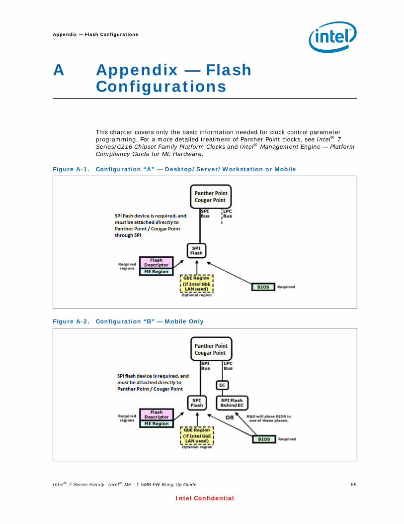
Intel® 7 Series Family- Intel® ME - 1.5MB FW Bring Up Guide 59
Intel Confidential
Appendix — Flash Configurations
A Appendix — Flash Configurations
This chapter covers only the basic information needed for clock control parameter programming. For a more detailed treatment of Panther Point clocks, see Intel® 7 Series/C216 Chipset Family Platform Clocks and Intel® Management Engine — Platform Compliancy Guide for ME Hardware.
Figure A-1. Configuration “A” — Desktop/Server/Workstation or Mobile
Figure A-2. Configuration “B” — Mobile Only

Intel® 7 Series Family- Intel® ME - 1.5MB FW Bring Up Guide 60
Intel Confidential
Appendix — Flash Configurations
§ §
Figure A-3. Configuration “C” — Desktop/Server/Workstation Only
Figure A-4. Configuration “D” — Mobile Only

Intel® 7 Series Family- Intel® ME - 1.5MB FW Bring Up Guide 61
Intel Confidential
Appendix — Intel® 7 Series/C216 Chipset Family Clock Configuration
B Appendix — Intel® 7 Series/C216 Chipset Family Clock Configuration
This chapter covers only the basic information needed for clock control parameter programming. For more information on validating and checking compliancy for PCH clocks, see Intel® 7 Series/C216 Chipset Family Intel® Management Engine — Compliancy Guide.
Note: 14.31818, 24, 25, 27 with SSC, 27 without SSC, and 48 MHz outputs are guaranteed from CLKOUTFLEX[3:0]. 25-MHz output cannot be used to supply Intel® LAN. 27 with SSC, 27 without SSC clocks are available in PCH hardware, but are not extensively tested or recommended for use.
Figure B-1. Intel® 7 Series/C216 Chipset Family Full Clock Integration Mode Architecture

Intel® 7 Series Family- Intel® ME - 1.5MB FW Bring Up Guide 62
Intel Confidential
Appendix — Intel® 7 Series/C216 Chipset Family Clock Configuration
B.1 Functional BlocksThere are 4 spread modulator in PCH, labeled as follows:
Note: By default, all the SSC blocks are configured to generate a spread spectrum of 0.5% down spread mode.
There are various clock dividers in PCH, labeled as follows:
Table B-1. SSC Blocks
Modulator Description
SSC1 Generates single phase 2.4-GHz output with spread for 120-MHz clock with spread generation by DIV1-S. Uses 2.4-GHz output of XCK PLL. Supplies CLKOUT_DP.
SSC2 Generates single phase 2.4-GHz output with spread for 100-MHz clock with spread and overclocking option generation by DIV2-S. Uses 2.4-GHz output of XCK PLL.Non-Overclocking: Supplies CLKOUT_DMI, CLKOUT_PEG[B:A], CLKOUT_ITPXDP, CLKOUT_SRC[7:0], and SATA. Indirectly supplies CLKOUT_PCI[4:0] and CLKOUTFLEX[3:0].Overclocking: Supplies CLKOUT_DMI, CLKOUT_PEG[B:A], and CLKOUT_ITPXDP only.
SSC3 Generates single phase 2.4-GHz output with spread for 100-MHz clock with spread and overclocking option generation by DIV3. Uses 2.4-GHz output of XCK PLL.Non-Overclocking: DisabledOverclocking: Supplies CLKOUT_SRC[7:0] and SATA. Indirectly supplies CLKOUT_PCI[4:0] and CLKOUTFLEX[3:0].
SSC4 Generates single phase 2.4-GHz output with spread for 120-MHz clock with spread and no overclocking option generation by DIV4. Uses 2.4-GHz output of XCK PLL.Non-Overclocking: Supplies SSSC clock for LVDS.Overclocking (some configurations): Supplies SATA.
Table B-2. Clock Dividers (Sheet 1 of 2)
Modulator Description
DIV1-NS Generates 120-MHz clock with no spread. Uses direct 2.4-GHz output of XCK PLL (not passed through SSC1). Supplies CLKOUT_DP.
DIV1-S Generates 120-MHz clock with spread. Uses output of SSC1. Can be no spread if SSC1 is disabled. Supplies CLKOUT_DP.
DIV2-NS Generates 100-MHz with no spread and overclocking option. Uses direct 2.4-GHz output of XCK PLL (not passed through SSC2).Disabled in all ME FW configurations.
DIV2-S Generates 100-MHz with spread and overclocking option. Uses output of SSC2. Can be no spread if SSC2 is disabled.Non-Overclocking: Supplies CLKOUT_DMI, CLKOUT_PEG[B:A], CLKOUT_ITPXDP, CLKOUT_SRC[7:0]. Indirectly supplies CLKOUT_PCI[4:0], SATA, and CLKOUTFLEX[3:0].Overclocking: Supplies CLKOUT_DMI, CLKOUT_PEG[B:A], CLKOUT_ITPXDP only.
DIV3 Generates 100-MHz with spread. Generally not expected to be overclocked. Uses output of SSC3. Can be no spread if SSC3 is disabled.Non-Overclocking: DisabledOverclocking: Supplies CLKOUT_SRC[7:0] only. Indirectly supplies CLKOUT_PCI[4:0], SATA, and CLKOUTFLEX[3:0].
DIV4 Generates 120-MHz clock with spread. Uses output of SSC4. Can be no spread if SSC4 is disabled. Supplies SATA. May also supply SSSC option for LVDS and utilized for Display Clock Bending.
DIV5A Generates 480-MHz clock which is then converted to 96-MHz clock by USBDIV1 (not shown). Uses 2.4-GHz output of XCK PLL. Supplies USBDIV1.
DIV5B Generates 96-MHz clock. Uses output of DIV5A. Supplies USB PLL.

Intel® 7 Series Family- Intel® ME - 1.5MB FW Bring Up Guide 63
Intel Confidential
Appendix — Intel® 7 Series/C216 Chipset Family Clock Configuration
B.2 Clock Configuration XMLNote: The use of ICC Configuration XML has been deprecated. Configuration of ICC
parameters are no longer available via separate XML file. The Flash Image Tool GUI can be used to edit ICC parameters.
B.3 Intel®ME FW Clock Control ParametersThe following parameters can be specified for Intel®ME FW programming. For more details on how to configure an SPI Flash image with these clock control parameters see the Bring Up Process chapter in the Firmware Bring Up Guide included in the Intel®ME FW kit.
B.3.1 CSS – Clock Source SelectAddress Offset: 0x00h
Flash Image Tool/ME FW Default for FCIM: 0001_1A33h Recommended Overclocking Default for FCIM: 0001_1A34h FCIM HW Default: 0001_1A12h
Description: This parameter controls clock source selection for non-PCI Express* clocks. Flash Image Tool Configuration: Available in ME Region | Configuration | ICC Data | ICC Profile 0 | FCIM/BTM Specific Registers
DIV6 Generates 48-Mhz or 24-MHz clock with no spread. Uses output of DIV5B. Supplies CLKOUTFLEX3.
DIV7 Generates 120-MHz clock with no spread. Uses output of USBDIV2B. Supplies CLKOUT_DP.
USBDIV1 Generates 96-MHz clock with no spread. Uses output of DIV5A. Supplies USB PLL.
USBDIV2A Generates 24- or 48-MHz clock with no spread. Uses 96-MHz output of DIV5B or USBDIV1 (not shown). Supplies CLKOUTFLEX3.
USBDIV2B Generates 240-MHz clock with no spread. Uses USB PLL’s 1.92 GHz clock output. Supplies DIV7.
DIVPCI Generates 33-MHz clock with spread. Uses output of either DIV2-S, DIV2-NS, or DIV4. Can be no spread if DIV2-NS is used or SSC4 is disabled. Supplies CLKOUT_PCI[4:0] and CLKOUTFLEX[3:0].
DIV14-REF Generates 14.318 MHz clock with no spread. Uses 2.4-GHz output of XCK PLL. Supplies CLKOUTFLEX[3:0].
Table B-2. Clock Dividers (Sheet 2 of 2)
Modulator Description

Intel® 7 Series Family- Intel® ME - 1.5MB FW Bring Up Guide 64
Intel Confidential
Appendix — Intel® 7 Series/C216 Chipset Family Clock Configuration
B.3.2 SSS – SRC Source SelectAddress Offset: 0x01h
Flash Image Tool/ME FW Default for FCIM: No changes from HW defaults Recommended Overclocking Default for FCIM: 0013_3744h FCIM HW Default: 0003_3733h
Description: This parameter controls clock source selection for PCI Express* clocks. Flash Image Tool Configuration: Available in ME Region | Configuration | ICC Data | ICC Profile 0 | FCIM/BTM Specific Registers
Table B-3. Clock Source Select Parameters
Bits Default Description
31:17 0h Reserved (RSVD)
16:12 10001b Chipset Configuration (PCHCFG): As specified by clock mode.
11:10 10b 24MHz/48MHz clock source select (24x48CSS): This field selects the source of 24/48 MHz clock used as a possible source for CLKOUTFLEX outputs. See “FLEXCLK[3:0] Source Select” parameters at FCSS (see Section B.3.3).
0xb = Reserved 10b = 48 MHz generated from XCK_PLL output divide 11b = 24 MHz generated from XCK_PLL output divide
9:3 HW: 42hME FW: 46hFITC: 46h
Chipset Configuration (PCHCFG): As specified by clock mode.
2:0 FCIMHW: 010b
ME FW: 011bFITC: 011b
FCIM OverclockingFITC: 100b
PCI Clock Source Select (PCSS): This field selects the source of 33-MHz clock used as a source for CLKOUT_PCI and CLKOUTFLEX outputs.
FCIM011b = SSC2 spread (non-overclocking option)
FCIM Overclocking100b = SSC3 (overclocking option)all other values = Reserved
Note: FCIM overclocking requires a parameter value different from FCIM ME FW defaults.Note: Spread spectrum can be turned on and off for SSC[3:2] using “SSC[3:2] Enable,
Active Low” parameters at SSCCTL[16,8] (see Section B.3.15).

Intel® 7 Series Family- Intel® ME - 1.5MB FW Bring Up Guide 65
Intel Confidential
Appendix — Intel® 7 Series/C216 Chipset Family Clock Configuration
B.3.3 FCSS – Flex Clock Source SelectAddress Offset: 0x02h
Flash Image Tool/ME FW Default: 0000_0232h HW Default: 0000_0304h
Table B-4. SRC Source Select Parameters
Bits Default Description
31:21 0h Reserved (RSVD)
20 FCIM0b
FCIM Overclocking1b
DMI Port Clock Select (DMIPORTCS): Selects PLL source for of 100-MHz clock used as a source for CLKOUT_DMI, CLKOUT_PEG_[B:A], and CLKOUT_ITPXDP outputs.
FCIM0b = Non-overclockable PXP PLLall other values = Reserved FCIM Overclocking1b = Overclockable DMI PLLall other values = Reserved
Note: FCIM overclocking requires a parameter value different from FCIM ME FW defaults.Note: 100-MHz clock used as a source for CLKOUT_SRC[7:0], and 33-MHz clock used as a
source for CLKOUT_PCI[4:0] and CLKOUTFLEX[3:0] are always sourced from non-overclockable PXP PLL.
19 0b Reserved (RSVD)
18:7 66Eh Chipset Configuration (PCHCFG): As specified by clock mode.
6:4 FCIM011b
FCIM Overclocking100b
SRC[7:4] Clock Source Select (SRC74CSS): This field selects the source of 100-MHz clock used as a source for CLKOUT_SRC[7:4] outputs.
FCIM011b = SSC2 spread (non-overclocking option)
FCIM Overclocking100b = SSC3 (overclocking option)all other values = Reserved
Note: FCIM overclocking requires a parameter value different from FCIM ME FW defaults.Note: Spread spectrum can be turned on and off for SSC[3:2] using “SSC[3:2] Enable,
Active Low” parameters at SSCCTL[16,8] (see Section B.3.15).
3 0b Reserved (RSVD)
2:0 FCIM011b
FCIM OverclockingFITC: 100b
SRC[3:0] Clock Source Select (SRC30CSS): This field selects the source of 100-MHz clock used as a source for CLKOUT_SRC[3:0] outputs.
FCIM011b = SSC2 spread (non-overclocking option)
FCIM Overclocking100b = SSC3 (overclocking option)all other values = Reserved
Note: FCIM overclocking requires a parameter value different from FCIM ME FW defaults.Note: Spread spectrum can be turned on and off for SSC[3:2] using “SSC[3:2] Enable,
Active Low” parameters at SSCCTL[16,8] (see Section B.3.15).

Intel® 7 Series Family- Intel® ME - 1.5MB FW Bring Up Guide 66
Intel Confidential
Appendix — Intel® 7 Series/C216 Chipset Family Clock Configuration
Description: This parameter controls muxing to select sources for Flex Clock outputs. Flash Image Tool Configuration: Available in ME Region | Configuration | ICC Data | ICC Profile 0 | ICC Registers
Note: For clock signal integrity reasons related to PCH power-related jitter, it is extremely important to follow the Flex Clock configuration guidelines:
• Prioritize 27/14/24/48/25-MHz FLEX on FLEX1 and FLEX3
• Do not configure 27/14/24/48/25-MHz FLEX clock on FLEX0 and FLEX2 if more than 2 PCI clocks + PCI loopback are routed.
• With 2 PCI clocks routed (or less), prioritize the FLEX clocks to FLEX1 and FLEX3 in this order (ie: first in the list = first to go to FLEX1 or FLEX3):
— 27 MHz Non-SSC and 27 MHz SSC— 14.31818 MHz— 48 MHz or 24 MHz or 25 MHz
Note: 27 with SSC, and 27 without SSC clocks are available in PCH hardware, but are not extensively tested by Intel® and are not recommended for use.
Table B-5. Flex Clock Source Select Parameters (Sheet 1 of 3)
Bits Default Description
31:15 0h Reserved (RSVD)
14:12 000b FLEXCLK3 Source Select (F3SS): Selects the source of clock to be driven out on CLKOUTFLEX3.000b = 24/48 MHz (24 or 48 determined by “24-MHz/48-MHz clock source” parameter at CSS[11:10], see Section B.3.1) 001b = 27 MHz Non-SSC, from DPLLB
— Requires “DPLLA/DPLLB/SSC1 Ownership” parameter at PLLEN[9] = 1b (see Section B.3.5)
— Requires “DPLLB VCO Enable” parameter at DPLLBC[30] = 1b010b = Reserved 011b = 14.31818 MHz 100b = Disabled (DC logic ‘0’) 101b = 27 MHz SSC, from DPLLA
— Requires “DPLLA/DPLLB/SSC1 Ownership” parameter at PLLEN[9] = 1b (see Section B.3.5)
— Requires “DPLLA VCO Enable” parameter at DPLLAC[30] = 1b— Requires “DPLLA Reference Select” parameter at DPLLAC[26:24] = 011b
110b = Disabled (DC logic ‘0’) 111b = Reserved
Note: 27 with SSC, and 27 without SSC clocks are available in PCH hardware, but are not extensively tested Intel® and are not recommended for use.
Note: This parameter field also controls the gating of 27-MHz clock source from DPLLB. When this clock is not being used, it is automatically gated off for power savings. When either “FLEXCLK3 or 2 Source Select” parameter field is set to 001b, 27-MHz clock from DPLLB is enabled and not gated.
Note: These clock select settings only take effect when this muxed FLEXCLK/GPIO pin is configured for FLEXCLK native usage. Refer to the Intel® 7 Series / 216 Chipset Family EDS for configuration of GPIO vs. native usage.
11 0b Reserved (RSVD)

Intel® 7 Series Family- Intel® ME - 1.5MB FW Bring Up Guide 67
Intel Confidential
Appendix — Intel® 7 Series/C216 Chipset Family Clock Configuration
10:8 011b FLEXCLK2 Source Select (F2SS): Selects the source of clock to be driven out on CLKOUTFLEX2.000b = 25 MHz from XCK PLL feedback path 001b = 27 MHz Non-SSC, from DPLLB
— Requires “DPLLA/DPLLB/SSC1 Ownership” parameter at PLLEN[9] = 1b (see Section B.3.5)
— Requires “DPLLB VCO Enable” parameter at DPLLBC[30] = 1b010b = 33.3 MHz 011b = 14.31818 MHz 100b = 24/48 MHz (24 or 48 determined by “24-MHz/48-MHz clock source” parameter at CSS[11:10], see Section B.3.1) 101b = 27 MHz SSC, from DPLLA
— Requires “DPLLA/DPLLB/SSC1 Ownership” parameter at PLLEN[9] = 1b (see Section B.3.5)
— Requires “DPLLA VCO Enable” parameter at DPLLAC[30] = 1b— Requires “DPLLA Reference Select” parameter at DPLLAC[26:24] = 011b
110b = Disabled (DC logic ‘0’) 111b = Reserved
Note: 27 with SSC, and 27 without SSC clocks are available in PCH hardware, but are not extensively tested Intel® and are not recommended for use.
Note: These clock select settings only take effect when this muxed FLEXCLK/GPIO pin is configured for FLEXCLK native usage. Refer to the Intel® 7 Series / 216 Chipset Family EDS for configuration of GPIO vs. native usage.
7 0b Reserved (RSVD)
Table B-5. Flex Clock Source Select Parameters (Sheet 2 of 3)
Bits Default Description

Intel® 7 Series Family- Intel® ME - 1.5MB FW Bring Up Guide 68
Intel Confidential
Appendix — Intel® 7 Series/C216 Chipset Family Clock Configuration
6:4 000b FLEXCLK1 Source Select (F1SS): Selects the source of clock to be driven out on CLKOUTFLEX1.000b = 001b = Reserved 010b = 011b = 14.31818 MHz 100b = 24/48 MHz (24 or 48 determined by “24-MHz/48-MHz clock source” parameter at CSS[11:10], see Section B.3.1) 101b = 27 MHz SSC, from DPLLA
— Requires “DPLLA/DPLLB/SSC1 Ownership” parameter at PLLEN[9] = 1b (see Section B.3.5)
— Requires “DPLLA VCO Enable” parameter at DPLLAC[30] = 1b— Requires “DPLLA Reference Select” parameter at DPLLAC[26:24] = 011b
110b = 27 MHz Non-SSC, from DPLLB— Requires “DPLLA/DPLLB/SSC1 Ownership” parameter at PLLEN[9] = 1b (see
Section B.3.5)— Requires “DPLLB VCO Enable” parameter at DPLLBC[30] = 1b
111b = Reserved
Note: 27 with SSC, and 27 without SSC clocks are available in PCH hardware, but are not extensively tested Intel® and are not recommended for use.
Note: These clock select settings only take effect when this muxed FLEXCLK/GPIO pin is configured for FLEXCLK native usage. Refer to the Intel® 7 Series / 216 Chipset FamilyEDS for configuration of GPIO vs. native usage.
3 0b Reserved (RSVD)
2:0 100b FLEXCLK0 Source Select (F0SS): Selects the source of clock to be driven out on CLKOUTFLEX0. 000b = 27 MHz SSC, from DPLLA
— Requires “DPLLA/DPLLB/SSC1 Ownership” parameter at PLLEN[9] = 1b (see Section B.3.5)
— Requires “DPLLA VCO Enable” parameter at DPLLAC[30] = 1b— Requires “DPLLA Reference Select” parameter at DPLLAC[26:24] = 011b
001b = Reserved 010b = 33.3 MHz 011b = 14.31818 MHz 100b = 24/48 MHz (24 or 48 determined by “24-MHz/48-MHz clock source” parameter at CSS[11:10], see Section B.3.1) 101b = Disabled (DC logic ‘0’) 110b = 27 MHz Non-SSC, from DPLLB
— Requires “DPLLA/DPLLB/SSC1 Ownership” parameter at PLLEN[9] = 1b (see Section B.3.5)
— Requires “DPLLB VCO Enable” parameter at DPLLBC[30] = 1b111b = Reserved
Note: 27 with SSC, and 27 without SSC clocks are available in PCH hardware, but are not extensively tested Intel® and are not recommended for use.
Note: This parameter field also controls the gating of 27-MHz clock source from DPLLA. When this clock is not being used, it is automatically gated off for power savings. When this parameter field is set to 000b, 27-MHz clock from DPLLA is enabled and not gated.
Note: These clock select settings only take effect when this muxed FLEXCLK/GPIO pin is configured for FLEXCLK native usage. Refer to the Intel® 7 Series / 216 Chipset Family EDS for configuration of GPIO vs. native usage.
Table B-5. Flex Clock Source Select Parameters (Sheet 3 of 3)
Bits Default Description

Intel® 7 Series Family- Intel® ME - 1.5MB FW Bring Up Guide 69
Intel Confidential
Appendix — Intel® 7 Series/C216 Chipset Family Clock Configuration
B.3.4 PLLRCS – PLL Reference Clock SelectAddress Offset: 0x03h
Flash Image Tool/ME FW Default for FCIM: 0008_8CBFh Recommended Overclocking Default for FCIM: 000A_8CBEh FCIM HW Default: 0008_8CBDh
Description: This parameter controls clock source selection for PCI Express* clocks. Flash Image Tool Configuration: Available in ME Region | Configuration | ICC Data | ICC Profile 0 | FCIM/BTM Specific Registers
Table B-6. PLL Reference Clock Select Parameters
Bits Default Description
31:20 0h Reserved (RSVD)
19 1b Chipset Configuration (PCHCFG): As specified by clock mode.
18:17 FCIM00b
FCIM Overclocking01b
SSCn Source Select for PXP PLL (SSCnSSPXPPLL): Selects the SSC source for use by PXP PLL.• In non-overclocking configurations, PXP PLL is expected to directly supply CLKOUT_DMI,
CLKOUT_PEG[B:A], CLKOUT_ITPXDP, CLKOUT_SRC[7:0], and SATA, and indirectly supply CLKOUT_PCI[4:0] and CLKOUTFLEX[3:0]
• In overclocking configurations, PXP PLL is expected to directly supply CLKOUT_SRC[7:0], and SATA, and indirectly supply CLKOUT_PCI[4:0] and CLKOUTFLEX[3:0]. DMI PLL is expected to supply CLKOUT_DMI, CLKOUT_PEG[B:A], CLKOUT_ITPXDP.
FCIM00b = SSC2all other values = Reserved FCIM Overclocking01b = SSC3all other values = Reserved
Note: FCIM overclocking requires a parameter value different from FCIM ME FW defaults.Note: Spread spectrum can be turned on and off for SSC[3:2] using “SSC[3:2] Enable,
Active Low” parameters at SSCCTL[16,8] (see Section B.3.15)
16:2 232Fh Chipset Configuration (PCHCFG): As specified by clock mode.
1:0 FCIM11b
FCIM Overclocking10b
SATA PLL Reference Select (SATARS): Selects the SSC/input pin source for use by SATA PLL.
FCIM11b = SSC2all other values = Reserved FCIM Overclocking10b = SSC3all other values = Reserved
Note: FCIM overclocking requires a parameter value different from FCIM ME FW defaults.Note: Spread spectrum can be turned on and off for SSC[3:2] using “SSC[3:2] Enable,
Active Low” parameters at SSCCTL[16,8] (see Section B.3.15).
Intel® 7 Series Family- Intel® ME - 1.5MB FW Bring Up Guide 70
Intel Confidential
Appendix — Intel® 7 Series/C216 Chipset Family Clock Configuration
B.3.5 DPLLAC – Display PLL “A” Configuration
Note: This parameter is not available in the Flash Image Tool GUI. If editing access to this parameter is required, consult Release Notes released with this Intel® ME FW kit for instructions.
B.3.6 DPLLBC – Display PLL “B” Configuration
Note: This parameter is not available in the Flash Image Tool GUI. If editing access to this parameter is required, consult Release Notes released with this Intel® ME FW kit for instructions.
B.3.7 PLLEN – PLL EnableAddress Offset: 0x0Ch
Flash Image Tool/ME FW Default for FCIM: 8000 000Ch FCIM Default: 80000404h (before PCH_PWROK), 8000040Ch (after PCH_PWROK)
Description: This parameter controls PLL enables. Flash Image Tool Configuration: Available in ME Region | Configuration | ICC Data | ICC Profile 0 | FCIM/BTM Specific Registers
B.3.8 OCKEN – Output Clock EnableAddress Offset: 0x0Eh
Flash Image Tool/ME FW Default: No changes from HW defaults HW Default: 1FFF_0F8Fh
Description: This parameter controls enabling of output buffers. Flash Image Tool Configuration: Available in ME Region | Configuration | ICC Data | ICC Profile 0 | ICC Registers
Table B-7. PLL Enable Parameters
Bits Default Description
31 0b Chipset Strap (PCHHWSTRP): Always reported as 1b.
30:11 0h Reserved (RSVD)
10 HW: 1bFITC: 0b
MEFW: 0b
SSC4 Ownership (SSC4OWN): Controls the owner of SSC4 and DIV4 (see Figure B-1).0b = Display Driver controls SSC4-associated resources.1b = ME controls SSC4-associated resources
9 0b DPLLA/DPLLB/SSC1 Ownership (DPLLSSC1OWN): Controls the owner of DPLLA, DPLLB, and SSC1.0b = Display Driver register set controls DPLLA, DPLLB, and SSC1 1b = ME FW controls DPLLA, DPLLB, and SSC1. This option must be selected if 27-MHz output is required from CLKOUTFLEX[3:0].
8:4 0h Reserved (RSVD)
3:0 Ch Chipset Configuration (PCHCFG): Must be set to Ch.

Intel® 7 Series Family- Intel® ME - 1.5MB FW Bring Up Guide 71
Intel Confidential
Appendix — Intel® 7 Series/C216 Chipset Family Clock Configuration
Table B-8. Output Clock Enable Parameters
Bits Default Description
31:29 0h Reserved (RSVD)
28 1b Chipset Configuration (PCHCFG): Must be set to 1b.
27 1b PEG_B Output Clock Enable (PBOCKEN): Controls the enabling of PEG_B clock toggling. When this clock output is not used, it should be gated to low state to save power.0b = Output clock is gated to low state 1b = Output buffer is enabled to toggle once its clock source has been initialized
26 1b PEG_A Output Clock Enable (PAOCKEN): Controls the enabling of PEG_A clock toggling. When this clock output is not used, it should be gated to low state to save power.0b = Output clock is gated to low state 1b = Output buffer is enabled to toggle once its clock source has been initialized
25 1b DP120 Output Clock Enable (DPOCKEN): Controls the enabling of CLKOUT_DP clock toggling. When this clock output is not used, it should be gated to low state to save power.0b = Output clock is gated to low state 1b = Output buffer is enabled to toggle once its clock source has been initializedNote: By default, the ownership of this bit is under display control. The display logic side (not ME FW) determines whether the output clock pin CLKOUT_DP toggles or gated to low state. Use the default value ‘1’ for this bit.
24 1b ITPXDP Output Clock Enable (ITPXDPOCKEN): Controls the enabling of CLKOUT_ITPXDP clock toggling. When this clock output is not used, it should be gated to low state to save power.0b = Output clock is gated to low state 1b = Output clock is enabled to toggle once its clock source has been initialized
23:16 FFh SRC 7:0 Output Clock Enable (SRC70OCKEN): Controls the enabling of SRC clock toggling. Each bit position controls the corresponding SRC output clock, e.g. bit 0 controls SRC0. When any clock output is not used, it should be gated to low state to save power.0b = Corresponding output clock is gated to low state 1b = Corresponding output clock is enabled to toggle once its clock source has been initialized (hot plug capable)
15:12 0h Reserved (RSVD)
11:7 1Fh PCICLK 4:0 Output Clock Enable (PCI40OCKEN): Controls the enabling of PCI clock toggling. Each bit position controls the corresponding PCI output clock, e.g. bit 7 controls CLKOUT_PCI0. When any clock output is not used, it should be gated to low state to save power.0b = Corresponding output clock is gated to low state 1b = Corresponding output clock is enabled to toggle once its clock source has been initializedA-stepping Note: This parameter has no effect and clock output is always enabled.B-stepping Note: Parameter behaves normally.
6:4 0h Reserved (RSVD)
3:0 Fh FLEXCLK 3:0 Output Clock Enable (FLEX30OCKEN): Controls the enabling of FLEXCLK toggling.Each bit position controls the corresponding FLEXCLK output clock, e.g. LSB (bit 0) controls CLKOUTFLEX0. When any clock output is not used, it should be gated to low state to save power.0b = Corresponding output clock is gated to low state 1b = Corresponding output clock is enabled to toggle once its clock source has been initialized

Intel® 7 Series Family- Intel® ME - 1.5MB FW Bring Up Guide 72
Intel Confidential
Appendix — Intel® 7 Series/C216 Chipset Family Clock Configuration
B.3.9 IBEN – Input Buffer EnableAddress Offset: 0x0Fh
Flash Image Tool/ME FW Default for FCIM: No changes from HW defaults FCIM Default: 0000_002Fh
Description: This parameter controls enabling of input buffers. Flash Image Tool Configuration: Available in ME Region | Configuration | ICC Data | ICC Profile 0 | FCIM/BTM Specific Registers
Table B-9. Input Buffer Enable Parameters
Bits Default Description
31:6 0h Reserved (RSVD)
5:4 10b CLKIN_SATA Input Buffer Disable (CKINSATAInBufDis): Controls the differential input buffer for CLKIN_SATA. When CLKIN_SATA is not used, its input buffer should be turned off for power saving.00b = CLKIN_SATA Differential Input Buffer is subjected to dynamic power management control by the SATA logic as part of the SATACLKREQ# protocol to the external clock generator. This setting is only applicable when CLKIN_SATA is configured to only source PCH SATA PLL but not source any other clock consumers. 01b = Input buffer is enabled 1xb = Input buffer is disabled for power saving
3 1b Chipset Configuration (PCHCFG): Must be set to 1b.
2 1b CLKIN_DMI Input Buffer Disable (CKINDMIInBufDis): Controls the differential input buffer for CLKIN_DMI. When CLKIN_DMI is not used, its input buffer should be turned off for power saving.0b = Input buffer is enabled 1b = Input buffer is disabled for power saving
1 1b CLKIN_DOT96 Input Buffer Disable (CKIN96InBufDis): Controls the differential input buffer for CLKIN_DOT96. When CLKIN_DOT96 is not used, its input buffer should be turned off for power saving.0b = Input buffer is enabled 1b = Input buffer is disabled for power saving
0 1b Chipset Configuration (PCHCFG): Set to 0b by hardware default (in BTM only), but required to be 1b.

Intel® 7 Series Family- Intel® ME - 1.5MB FW Bring Up Guide 73
Intel Confidential
Appendix — Intel® 7 Series/C216 Chipset Family Clock Configuration
B.3.10 DIVEN – Divider EnableAddress Offset: 0x10h
Flash Image Tool/ME FW Default for FCIM: 0000_05EBh FCIM Default: 00000DFFh
Description: This parameter controls enabling of divider blocks. Flash Image Tool Configuration: Available in ME Region | Configuration | ICC Data | ICC Profile 0 | FCIM/BTM Specific Registers
Table B-10. Divider Enable Parameters
Bits Default Description
31:12 0h Reserved (RSVD)
11 HW: 1bME FW: 0bFITC: 0b
Chipset Configuration (PCHCFG): Set to 1b by hardware default, but required to be 0b (in FCIM only).
10 1b 14.31818Mhz Fractional Divisor Enable (14FDEN): Enables fractional divisor for 14.31818Mhz clock generation (see Figure B-1). When not used, the fractional divisor can be disabledfor power saving.0b = Divider is disabled1b = Divider is enabled
Note: PCH use the 14.31818Mhz Fraction divisor to provide clock for PCH internal legacy 8254, and PM timers. Turning off the 14.31818Mhz Fraction divisor will turn off clock to the PCH legacy 8254, and PM timers. The 14.31818Mhz Fraction divisor should NOT be turn off even if it is not used externally .
9 0b Reserved (RSVD)
8 1b DIV7 Enable (DIV7EN): Enables DIV7 clock divider (see Figure B-1).0b = Divider is enabled (120 Mhz generated from USB PLL) 1b = Divider is disabled (120Mhz generated by XCK PLL)
7 1b DIV5 Stage 2 Enable (DIV5BEN): Enables DIV5B clock divider (see Figure B-1).0b = Divider is disabled 1b = Divider is enabled
6 1b DIV5 Stage 1 Enable (DIV5AEN): Enables DIV5A clock divider (see Figure B-1).0b = Divider is disabled 1b = Divider is enabled
5 1b DIV4 Enable (DIV4EN): Enables DIV4 clock divider (see Figure B-1).0b = Divider is disabled 1b = Divider is enabled
4 HW: 1bME FW: 0bFITC: 0b
DIV3 Enable (DIV3EN): Enables DIV3 clock divider (see Figure B-1).0b = Divider is disabled 1b = Divider is enabled
3 1b DIV2-S Enable (DIV2SEN): Enables DIV2-S clock divider (see Figure B-1).0b = Divider is disabled 1b = Divider is enabled
2 HW: 1bME FW: 0bFITC: 0b
DIV2-NS Enable (DIV2NSEN): Enables DIV2-NS clock divider (see Figure B-1).0b = Divider is disabled 1b = Divider is enabled
1 1b DIV1-S Enable (DIV1SEN): Enables DIV1-S clock divider (see Figure B-1).0b = Divider is disabled 1b = Divider is enabled
0 1b DIV1-NS Enable (DIV1NSEN): Enables DIV1-NS clock divider (see Figure B-1).0b = Divider is disabled 1b = Divider is enabled

Intel® 7 Series Family- Intel® ME - 1.5MB FW Bring Up Guide 74
Intel Confidential
Appendix — Intel® 7 Series/C216 Chipset Family Clock Configuration
B.3.11 PM1 – Power ManagementAddress Offset: 0x12h
Flash Image Tool/ME FW Default: 0000_001Fh HW Default: 0000_0000h
Description: This parameter controls power management features of clocks. Flash Image Tool Configuration: Available in ME Region | Configuration | ICC Data | ICC Profile 0 | ICC Registers
B.3.12 PM2 – Power ManagementAddress Offset: 0x13h
Table B-11. Power Management Parameters
Bits Default Description
31:5 0h Reserved (RSVD)
4 HW: 0bME FW: 1bFITC: 1b
Dynamic SSC1 Shutdown Enable (SSC1DSEN): Enables dynamic power management of DIV1-S (see Figure B-1, page 61).• Integrated Graphics Device Display Driver may dynamically power manage SSC1 when:
— Integrated Graphics Device Display Driver is assigned ownership of SSC1 (“DPLLA/DPLLB/SSC1 Ownership” parameter field at PLLEN[9] = 0b, see Section B.3.5)
— SSC1 is globally enabled (“SSC1 Enable, Active Low” parameter field at SSCCTL[0] = 0b)
• This bit has no effect, (dynamic power management of DIV4 can only be performed through Intel® MEI message SET_ICC_REGISTER from BIOS during POST and S3 resume, not by Integrated Graphics Device Display Driver), when:
— ME is assigned ownership (PLLEN[9] = 1b, see Section B.3.5).The following are logical combinations of this parameter field (MSB) and “Dynamic DIV1S Shutdown Enable” parameter at PM1[0] (LSB).00b = Disable dynamic management of DIV1-S and SSC1 01b = Dynamic management of DIV1-S only. SSC1 stays up and maintains current state for lower clock recovery latency at the expense of power. 10b = Reserved 11b = Dynamic management of both DIV1-S and SSC1. Longer clock recovery latency but more power savings.
3:2 HW: 00bME FW: 11bFITC: 11b
Dynamic SSC4 and DIV4 Shutdown Enable (SSC4DIV4DSEN): Enables dynamic power management of SSC4 and DIV4 (see Figure B-1, page 61).• Integrated Graphics Device Display Driver may dynamically power manage SSC4 when:
— Integrated Graphics Device Display Driver is assigned ownership of SSC4 (“SSC4 Ownership” parameter at PLLEN[10] = 0b, see Section B.3.5)
— SSC4 is globally enabled (“SSC4 Enable, Active Low” parameter field at SSCCTL[24] = 0b, see Section B.3.5)
• This bit has no effect, (dynamic power management of DIV4 can only be performed through Intel® MEI message SET_ICC_REGISTER from BIOS during POST and S3 resume, not by Integrated Graphics Device Display Driver), when:
— ME is assigned ownership (PLLEN[10] = 1b, see Section B.3.5)00b = Disable dynamic management of DIV4 and SSC4 01b = Dynamic management of DIV4 only. SSC4 stays up and maintains current state for lower clock recovery latency at the expense of power. 10b = Reserved 11b = Dynamic management of both DIV4 and SSC4. Longer clock recovery latency but more power savings.
1 HW: 0bME FW: 1bFITC: 1b
Dynamic DIV1-NS Shutdown Enable (DIV1NSDSEN): Enables dynamic power management of DIV1-NS (see Figure B-1).0b = Disable dynamic power management of DIV1-S 1b = Enable dynamic power management of DIV1-S
0 HW: 0bME FW: 1bFITC: 1b
Dynamic DIV1-S Shutdown Enable (DIV1SDSEN): Enables dynamic power management of DIV1-S (see Figure B-1).Note: Do not configure this parameter field on its own. See “DIV1 Shutdown Enable”
parameter at PM1[4].

Intel® 7 Series Family- Intel® ME - 1.5MB FW Bring Up Guide 75
Intel Confidential
Appendix — Intel® 7 Series/C216 Chipset Family Clock Configuration
Flash Image Tool/ME FW Default: No changes from HW defaults HW Default: 0000_0000h
Description: This parameter controls power management features of clocks. Flash Image Tool Configuration: Available in ME Region | Configuration | ICC Data | ICC Profile 0 | ICC Registers
B.3.13 SEBP1 – Single Ended Buffer ParametersAddress Offset: 0x1Ch
Flash Image Tool/ME FW Default: No changes from HW defaults HW Default: 0000_9999h
Description: This parameter controls double/single load series resistance and slew rate for FLEX clocks. Flash Image Tool Configuration: Not present in Flash Image Tool
Table B-12. Power Management Parameters
Bits Default Description
31:9 0h Reserved (RSVD)
8:5 0000b CLKRUN Control Enable for PCI 33 Mhz on CLKOUTFLEX (CLKRUNCEN_FLEX): Enables support for CLKRUN protocol for PCI 33 MHz clocks muxed out to CLKOUTFLEX[3:0].0b = Corresponding CLKOUTFLEX PCI clock is free-running, unaffected by CLKRUN protocol 1b = Corresponding CLKOUTFLEX PCI clock is shut off when CLKRUN protocol turns off PCI clocksNote: These bits must be clear (0b) when the corresponding CLKOUTFLEX pins are not configured for PCI 33Mhz clock.
4:0 0 0000b CLKRUN Control Enable (CLKRUNCEN): Enables support for CLKRUN protocol for CLKOUT_PCI[4:0].0b = Corresponding CLKOUT_PCI is free-running, unaffected by CLKRUN protocol 1b = Corresponding CLKOUT_PCI is shut off when CLKRUN protocol turns off PCI clocksNote: This parameter does not enable CLKRUN protocol support for CLKOUTFLEX[3:0].
Table B-13. Single Ended Buffer Parameters (Sheet 1 of 2)
Bits Default Description
31:16 0h Reserved (RSVD)
15:13 100b FLEXCLK3 Slew Rate Control (F3SLC): Controls slew rate for CLKOUTFLEX3.000b = Weakest slew rate setting (~0.6 V/ns for a TBD inch trace at double load) 001b 010b 011b 100b = Default Slew rate setting (~1.4V/ns for a TBD inch trace at double load) 101b 110b 111b = Strongest slew rate setting (~2 V/ns for a TBD inch trace at double load)
12 1b FLEXCLK3 Single/Double Load Series Resistance (F3SDLSR): Sets programmable series resistance for CLKOUTFLEX3.0b = 25 Ohms for single load usage 1b = 17 Ohms for double load usage

Intel® 7 Series Family- Intel® ME - 1.5MB FW Bring Up Guide 76
Intel Confidential
Appendix — Intel® 7 Series/C216 Chipset Family Clock Configuration
B.3.14 SEBP2 – Single Ended Buffer ParametersAddress Offset: 0x1Dh
Flash Image Tool/ME FW Default: No changes from HW defaults HW Default: 0009_9999h
Description: This parameter controls double/single load series resistance and slew rate for PCI clocks. PCI Specifications 2.4 and 3.0 allow for an acceptable slew rate range of 1 to 4 V/ns. ME FW programmability allows for slew rate to be specified between 0.6 to 2 V/ns for two reasons:
1. Slew rates exceeding 2 V/ns can have adverse effects on platform EMI2. Slew rates lower than 1 V/ns can be specified for EMI benefits, at the risk of
violating PCI specification
Flash Image Tool Configuration: Available in ME Region | Configuration | ICC Data | ICC Profile 0 | ICC Registers
11:9 100b FLEXCLK2 Slew Rate Control (F2SLC): Controls slew rate for CLKOUTFLEX2.000b = Weakest slew rate setting (~0.6 V/ns for a TBD inch trace at double load) 001b 010b 011b 100b = Default Slew rate setting (~1.4V/ns for a TBD inch trace at double load) 101b 110b 111b = Strongest slew rate setting (~2 V/ns for a TBD inch trace at double load)
8 1b FLEXCLK2 Single/Double Load Series Resistance (F2SDLSR): Sets programmable series resistance for CLKOUTFLEX2.0b = 25 Ohms for single load usage 1b = 17 Ohms for double load usage
7:5 100b FLEXCLK1 Slew Rate Control (F1SLC): Controls slew rate for CLKOUTFLEX1.000b = Weakest slew rate setting (~0.6 V/ns for a TBD inch trace at double load) 001b 010b 011b 100b = Default Slew rate setting (~1.4V/ns for a TBD inch trace at double load) 101b 110b 111b = Strongest slew rate setting (~2 V/ns for a TBD inch trace at double load)
4 1b FLEXCLK1 Single/Double Load Series Resistance (F1SDLSR): Sets programmable series resistance for CLKOUTFLEX1.0b = 25 Ohms for single load usage 1b = 17 Ohms for double load usage
3:1 100b FLEXCLK0 Slew Rate Control (F2SLC): Controls slew rate for CLKOUTFLEX2.000b = Weakest slew rate setting (~0.6 V/ns for a TBD inch trace at double load) 001b 010b 011b 100b = Default Slew rate setting (~1.4V/ns for a TBD inch trace at double load) 101b 110b 111b = Strongest slew rate setting (~2 V/ns for a TBD inch trace at double load)
0 1b FLEXCLK0 Single/Double Load Series Resistance (F0SDLSR): Sets programmable series resistance for CLKOUTFLEX0.0b = 25 Ohms for single load usage 1b = 17 Ohms for double load usage
Table B-13. Single Ended Buffer Parameters (Sheet 2 of 2)
Bits Default Description

Intel® 7 Series Family- Intel® ME - 1.5MB FW Bring Up Guide 77
Intel Confidential
Appendix — Intel® 7 Series/C216 Chipset Family Clock Configuration
Table B-14. Single Ended Buffer Parameters (Sheet 1 of 2)
Bits Default Description
31:20 0h Reserved (RSVD)
19:17 100b PCI4 Slew Rate Control (PCI4SLC): Controls slew rate for CLKOUTPCI4.000b = Weakest slew rate setting (~0.6 V/ns for a TBD inch trace at double load) 001b 010b 011b 100b = Default Slew rate setting (~1.4V/ns for a TBD inch trace at double load) 101b 110b 111b = Strongest slew rate setting (~2 V/ns for a TBD inch trace at double load)
16 1b PCI4 Single/Double Load Series Resistance (PCI4SDLSR): Sets programmable series resistance for CLKOUT_PCI4.0b = 25 Ohms for single load usage 1b = 17 Ohms for double load usage
15:13 100b PCI3 Slew Rate Control (PCI3SLC): Controls slew rate for CLKOUT_PCI3.000b = Weakest slew rate setting (~0.6 V/ns for a TBD inch trace at double load) 001b 010b 011b 100b = Default Slew rate setting (~1.4V/ns for a TBD inch trace at double load) 101b 110b 111b = Strongest slew rate setting (~2 V/ns for a TBD inch trace at double load)
12 1b PCI3 Single/Double Load Series Resistance (PCI3SDLSR): Sets programmable series resistance for CLKOUT_PCI3.0b = 25 Ohms for single load usage 1b = 17 Ohms for double load usage
11:9 100b PCI2 Slew Rate Control (PCI2SLC): Controls slew rate for CLKOUT_PCI2.000b = Weakest slew rate setting (~0.6 V/ns for a TBD inch trace at double load) 001b 010b 011b 100b = Default Slew rate setting (~1.4V/ns for a TBD inch trace at double load) 101b 110b 111b = Strongest slew rate setting (~2 V/ns for a TBD inch trace at double load)
8 1b PCI2 Single/Double Load Series Resistance (PCI2SDLSR): Sets programmable series resistance for CLKOUT_PCI2.0b = 25 Ohms for single load usage 1b = 17 Ohms for double load usage
7:5 100b PCI1 Slew Rate Control (PCI1SLC): Controls slew rate for CLKOUT_PCI1.000b = Weakest slew rate setting (~0.6 V/ns for a TBD inch trace at double load) 001b 010b 011b 100b = Default Slew rate setting (~1.4V/ns for a TBD inch trace at double load) 101b 110b 111b = Strongest slew rate setting (~2 V/ns for a TBD inch trace at double load)

Intel® 7 Series Family- Intel® ME - 1.5MB FW Bring Up Guide 78
Intel Confidential
Appendix — Intel® 7 Series/C216 Chipset Family Clock Configuration
B.3.15 SSCCTL – SSC ControlAddress Offset: 0x24h
Flash Image Tool/ME FW Default for FCIM: 0001_0000h FCIM Default: 0000_0000h
Description: This parameter controls spread spectrum modulation capability of SSC blocks. Flash Image Tool Configuration: Available in ME Region | Configuration | ICC Data | ICC Profile 0 | FCIM/BTM Specific Registers
4 1b PCI1 Single/Double Load Series Resistance (PCI1SDLSR): Sets programmable series resistance for CLKOUT_PCI1.0b = 25 Ohms for single load usage 1b = 17 Ohms for double load usage
3:1 100b PCI0 Slew Rate Control (PCI0SLC): Controls slew rate for CLKOUT_PCI0.000b = Weakest slew rate setting (~0.6 V/ns for a TBD inch trace at double load) 001b 010b 011b 100b = Default Slew rate setting (~1.4V/ns for a TBD inch trace at double load) 101b 110b 111b = Strongest slew rate setting (~2 V/ns for a TBD inch trace at double load)
0 1b PCI0 Single/Double Load Series Resistance (PCI0SDLSR): Sets programmable series resistance for CLKOUT_PCI0.0b = 25 Ohms for single load usage 1b = 17 Ohms for double load usage
Table B-14. Single Ended Buffer Parameters (Sheet 2 of 2)
Bits Default Description
Table B-15. SSC Control Parameters (Sheet 1 of 2)
Bits Default Description
31:27 0h Reserved (RSVD)
26:25 00b SSC4 Spread Mode (SSC4_SprdMd): Select the spread mode for SSC4.00b = Down spread 01b = Center spread 10b = Reserved 11b = Reserved
24 0b SSC4 Enable, Active Low (SSC4_EnB): Determines whether SSC4 (see Figure B-1, page 61) is enabled.0b = Enable SSC4 1b = Power off SSC4 and select bypass path to SSC4 output. SSC4 output will thus be non-spread.
23:19 0h Reserved (RSVD)
18:17 00b SSC3 Spread Mode (SSC3_SprdMd): Select the spread mode for SSC3.00b = Down spread 01b = Center spread 10b = Reserved 11b = Reserved
16 0b SSC3 Enable, Active Low (SSC3_EnB): Determines whether SSC3 (see Figure B-1, page 61) is enabled.0b = Enable SSC3 1b = Power off SSC3 and select bypass path to SSC3 output. SSC3 output will thus be non-spread.
15:11 0h Reserved (RSVD)

Intel® 7 Series Family- Intel® ME - 1.5MB FW Bring Up Guide 79
Intel Confidential
Appendix — Intel® 7 Series/C216 Chipset Family Clock Configuration
B.3.16 PMSRCCLK1 – SRC Power ManagementAddress Offset: 0x48h
Flash Image Tool/ME FW Default: No changes from HW defaults HW Default: 7654_3210h
Description: This parameter as signs dynamic CLKRQ# control of SRC clocks. Flash Image Tool Configuration: Available in ME Region | Configuration | ICC Data | ICC Profile 0 | ICC Registers
10:9 00b SSC2 Spread Mode (SSC2_SprdMd): Select the spread mode for SSC2.00b = Down spread 01b = Center spread 10b = Reserved 11b = Reserved
8 0b SSC2 Enable, Active Low (SSC2_EnB): Determines whether SSC2 (see Figure B-1, page 61) is enabled.0b = Enable SSC2 1b = Power off SSC2 and select bypass path to SSC2 output. SSC2 output will thus be non-spread.
7:3 0h Reserved (RSVD)
2:1 00b SSC1 Spread Mode (SSC1_SprdMd): Select the spread mode for SSC1.00b = Down spread 01b = Center spread 10b = Reserved 11b = Reserved
0 0b SSC1 Enable, Active Low (SSC1_EnB): Determines whether SSC1 (see Figure B-1, page 61) is enabled.0b = Enable SSC1 1b = Power off SSC1 and select bypass path to SSC1 output. SSC1 output will thus be non-spread.
Table B-15. SSC Control Parameters (Sheet 2 of 2)
Bits Default Description

Intel® 7 Series Family- Intel® ME - 1.5MB FW Bring Up Guide 80
Intel Confidential
Appendix — Intel® 7 Series/C216 Chipset Family Clock Configuration
Table B-16. SRC Power Management (Sheet 1 of 2)
Bits Default Description
31:28 0111b CLKRQ# Select for CLKOUT_SRC7 (CRQSELSRC7): Select external input CLKRQ# pin for dynamic control of CLKOUT_SRC7 output.0000b = SRC0CLKRQ#/GPIO73 controls CLKOUT_SRC7 0001b = SRC1CLKRQ#/GPIO18 controls CLKOUT_SRC7 0010b = SRC2CLKRQ#/GPIO20 controls CLKOUT_SRC7 0011b = SRC3CLKRQ#/GPIO25 controls CLKOUT_SRC7 0100b = SRC4CLKRQ#/GPIO26 controls CLKOUT_SRC7 0101b = SRC5CLKRQ#/GPIO44 controls CLKOUT_SRC7 0110b = SRC6CLKRQ#/GPIO45 controls CLKOUT_SRC7 0111b = SRC7CLKRQ#/GPIO46 controls CLKOUT_SRC7 1000b = SRC8CLKRQ#/PEG_A_CLKRQ#/GPIO47 controls CLKOUT_SRC7 1001b = SRC9CLKRQ#/PEG_B_CLKRQ#/GPIO56 controls CLKOUT_SRC7 1x1xb = Reserved
27:24 0110b CLKRQ# Select for CLKOUT_SRC6 (CRQSELSRC6): Select external input CLKRQ# pin for dynamic control of CLKOUT_SRC6 output.0000b = SRC0CLKRQ#/GPIO73 controls CLKOUT_SRC6 0001b = SRC1CLKRQ#/GPIO18 controls CLKOUT_SRC6 0010b = SRC2CLKRQ#/GPIO20 controls CLKOUT_SRC6 0011b = SRC3CLKRQ#/GPIO25 controls CLKOUT_SRC6 0100b = SRC4CLKRQ#/GPIO26 controls CLKOUT_SRC6 0101b = SRC5CLKRQ#/GPIO44 controls CLKOUT_SRC6 0110b = SRC6CLKRQ#/GPIO45 controls CLKOUT_SRC6 0111b = SRC7CLKRQ#/GPIO46 controls CLKOUT_SRC6 1000b = SRC8CLKRQ#/PEG_A_CLKRQ#/GPIO47 controls CLKOUT_SRC6 1001b = SRC9CLKRQ#/PEG_B_CLKRQ#/GPIO56 controls CLKOUT_SRC6 1x1xb = Reserved
23:20 0101b CLKRQ# Select for CLKOUT_SRC5 (CRQSELSRC5): Select external input CLKRQ# pin for dynamic control of CLKOUT_SRC5 output.0000b = SRC0CLKRQ#/GPIO73 controls CLKOUT_SRC5 0001b = SRC1CLKRQ#/GPIO18 controls CLKOUT_SRC5 0010b = SRC2CLKRQ#/GPIO20 controls CLKOUT_SRC5 0011b = SRC3CLKRQ#/GPIO25 controls CLKOUT_SRC5 0100b = SRC4CLKRQ#/GPIO26 controls CLKOUT_SRC5 0101b = SRC5CLKRQ#/GPIO44 controls CLKOUT_SRC5 0110b = SRC6CLKRQ#/GPIO45 controls CLKOUT_SRC5 0111b = SRC7CLKRQ#/GPIO46 controls CLKOUT_SRC5 1000b = SRC8CLKRQ#/PEG_A_CLKRQ#/GPIO47 controls CLKOUT_SRC5 1001b = SRC9CLKRQ#/PEG_B_CLKRQ#/GPIO56 controls CLKOUT_SRC5 1x1xb = Reserved
19:16 0100b CLKRQ# Select for CLKOUT_SRC4 (CRQSELSRC4): Select external input CLKRQ# pin for dynamic control of CLKOUT_SRC4 output.0000b = SRC0CLKRQ#/GPIO73 controls CLKOUT_SRC4 0001b = SRC1CLKRQ#/GPIO18 controls CLKOUT_SRC4 0010b = SRC2CLKRQ#/GPIO20 controls CLKOUT_SRC4 0011b = SRC3CLKRQ#/GPIO25 controls CLKOUT_SRC4 0100b = SRC4CLKRQ#/GPIO26 controls CLKOUT_SRC4 0101b = SRC5CLKRQ#/GPIO44 controls CLKOUT_SRC4 0110b = SRC6CLKRQ#/GPIO45 controls CLKOUT_SRC4 0111b = SRC7CLKRQ#/GPIO46 controls CLKOUT_SRC4 1000b = SRC8CLKRQ#/PEG_A_CLKRQ#/GPIO47 controls CLKOUT_SRC4 1001b = SRC9CLKRQ#/PEG_B_CLKRQ#/GPIO56 controls CLKOUT_SRC4 1x1xb = Reserved
15:12 0011b CLKRQ# Select for CLKOUT_SRC3 (CRQSELSRC3): Select external input CLKRQ# pin for dynamic control of CLKOUT_SRC3 output.0000b = SRC0CLKRQ#/GPIO73 controls CLKOUT_SRC3 0001b = SRC1CLKRQ#/GPIO18 controls CLKOUT_SRC3 0010b = SRC2CLKRQ#/GPIO20 controls CLKOUT_SRC3 0011b = SRC3CLKRQ#/GPIO25 controls CLKOUT_SRC3 0100b = SRC4CLKRQ#/GPIO26 controls CLKOUT_SRC3 0101b = SRC5CLKRQ#/GPIO44 controls CLKOUT_SRC3 0110b = SRC6CLKRQ#/GPIO45 controls CLKOUT_SRC3 0111b = SRC7CLKRQ#/GPIO46 controls CLKOUT_SRC3 1000b = SRC8CLKRQ#/PEG_A_CLKRQ#/GPIO47 controls CLKOUT_SRC3 1001b = SRC9CLKRQ#/PEG_B_CLKRQ#/GPIO56 controls CLKOUT_SRC3 1x1xb = Reserved
Intel® 7 Series Family- Intel® ME - 1.5MB FW Bring Up Guide 81
Intel Confidential
Appendix — Intel® 7 Series/C216 Chipset Family Clock Configuration
B.3.17 PMSRCCLK2 – SRC Power ManagementAddress Offset: 0x49h
Flash Image Tool/ME FW Default: No changes from HW defaults HW Default: 0000_0F98h
Description: This parameter assigns dynamic CLKRQ# control of SRC clocks. Flash Image Tool Configuration: Available in ME Region | Configuration | ICC Data | ICC Profile 0 | ICC Registers
11:8 0010b CLKRQ# Select for CLKOUT_SRC2 (CRQSELSRC2): Select external input CLKRQ# pin for dynamic control of CLKOUT_SRC2 output.0000b = SRC0CLKRQ#/GPIO73 controls CLKOUT_SRC2 0001b = SRC1CLKRQ#/GPIO18 controls CLKOUT_SRC2 0010b = SRC2CLKRQ#/GPIO20 controls CLKOUT_SRC2 0011b = SRC3CLKRQ#/GPIO25 controls CLKOUT_SRC2 0100b = SRC4CLKRQ#/GPIO26 controls CLKOUT_SRC2 0101b = SRC5CLKRQ#/GPIO44 controls CLKOUT_SRC2 0110b = SRC6CLKRQ#/GPIO45 controls CLKOUT_SRC2 0111b = SRC7CLKRQ#/GPIO46 controls CLKOUT_SRC2 1000b = SRC8CLKRQ#/PEG_A_CLKRQ#/GPIO47 controls CLKOUT_SRC2 1001b = SRC9CLKRQ#/PEG_B_CLKRQ#/GPIO56 controls CLKOUT_SRC2 1x1xb = Reserved
7:4 0001b CLKRQ# Select for CLKOUT_SRC1 (CRQSELSRC1): Select external input CLKRQ# pin for dynamic control of CLKOUT_SRC1 output.0000b = SRC0CLKRQ#/GPIO73 controls CLKOUT_SRC1 0001b = SRC1CLKRQ#/GPIO18 controls CLKOUT_SRC1 0010b = SRC2CLKRQ#/GPIO20 controls CLKOUT_SRC1 0011b = SRC3CLKRQ#/GPIO25 controls CLKOUT_SRC1 0100b = SRC4CLKRQ#/GPIO26 controls CLKOUT_SRC1 0101b = SRC5CLKRQ#/GPIO44 controls CLKOUT_SRC1 0110b = SRC6CLKRQ#/GPIO45 controls CLKOUT_SRC1 0111b = SRC7CLKRQ#/GPIO46 controls CLKOUT_SRC1 1000b = SRC8CLKRQ#/PEG_A_CLKRQ#/GPIO47 controls CLKOUT_SRC1 1001b = SRC9CLKRQ#/PEG_B_CLKRQ#/GPIO56 controls CLKOUT_SRC1 1x1xb = Reserved
3:0 0000b CLKRQ# Select for CLKOUT_SRC0 (CRQSELSRC0): Select external input CLKRQ# pin for dynamic control of CLKOUT_SRC0 output.0000b = SRC0CLKRQ#/GPIO73 controls CLKOUT_SRC0 0001b = SRC1CLKRQ#/GPIO18 controls CLKOUT_SRC0 0010b = SRC2CLKRQ#/GPIO20 controls CLKOUT_SRC0 0011b = SRC3CLKRQ#/GPIO25 controls CLKOUT_SRC0 0100b = SRC4CLKRQ#/GPIO26 controls CLKOUT_SRC0 0101b = SRC5CLKRQ#/GPIO44 controls CLKOUT_SRC0 0110b = SRC6CLKRQ#/GPIO45 controls CLKOUT_SRC0 0111b = SRC7CLKRQ#/GPIO46 controls CLKOUT_SRC0 1000b = SRC8CLKRQ#/PEG_A_CLKRQ#/GPIO47 controls CLKOUT_SRC0 1001b = SRC9CLKRQ#/PEG_B_CLKRQ#/GPIO56 controls CLKOUT_SRC0 1x1xb = Reserved
Table B-16. SRC Power Management (Sheet 2 of 2)
Bits Default Description

Intel® 7 Series Family- Intel® ME - 1.5MB FW Bring Up Guide 82
Intel Confidential
Appendix — Intel® 7 Series/C216 Chipset Family Clock Configuration
Table B-17. SRC Power Management
Bits Default Description
31:27 0h Reserved (RSVD)
26 0b CLKRQ# Control Enable for CLKOUT_ITPXDP: Enables support for CLKRQ# power management control for PCI Express* clock output to CLKOUT_ITPXDP.0b = Disable dynamic control of CLKOUT_ITPXDP clock 1b = CLKOUT_ITPXDP clock is dynamically controlled by assigned CLKRQ# pin
25 0b CLKRQ# Control Enable for CLKOUT_PEG_B: Enables support for CLKRQ# power management control for PCI Express* clock output to CLKOUT_PEG_B.0b = Disable dynamic control of corresponding CLKOUT_SRC clock 1b = CLKOUT_PEG_B clock is dynamically controlled by assigned CLKRQ# pin
24 0b CLKRQ# Control Enable for CLKOUT_PEG_A: Enables support for CLKRQ# power management control for PCI Express* clock output to CLKOUT_PEG_A.0b = Disable dynamic control of corresponding CLKOUT_SRC clock 1b = CLKOUT_PEG_A clock is dynamically controlled by assigned CLKRQ# pin
23:16 0000 0000b CLKRQ# Control Enable for CLKOUT_SRC[7:0]: Enables support for CLKRQ# power management control for PCI Express* clock outputs to CLKOUT_SRC[7:0].0b = Disable dynamic control of corresponding CLKOUT_SRC clock 1b = Corresponding CLKOUT_SRC clock is dynamically controlled by assigned CLKRQ# pin
15:12 0h Reserved (RSVD)
11:8 1111b CLKRQ# Select for CLKOUT_ITPXDP (CRQSELITPXDP): Select external input CLKRQ# pin for dynamic control of CLKOUT_SRC7 output.0000b = SRC0CLKRQ#/GPIO73 controls CLKOUT_ITPXDP 0001b = SRC1CLKRQ#/GPIO18 controls CLKOUT_ITPXDP 0010b = SRC2CLKRQ#/GPIO20 controls CLKOUT_ITPXDP 0011b = SRC3CLKRQ#/GPIO25 controls CLKOUT_ITPXDP 0100b = SRC4CLKRQ#/GPIO26 controls CLKOUT_ITPXDP 0101b = SRC5CLKRQ#/GPIO44 controls CLKOUT_ITPXDP 0110b = SRC6CLKRQ#/GPIO45 controls CLKOUT_ITPXDP 0111b = SRC7CLKRQ#/GPIO46 controls CLKOUT_ITPXDP 1000b = SRC8CLKRQ#/PEG_A_CLKRQ#/GPIO47 controls CLKOUT_ITPXDP 1001b = SRC9CLKRQ#/PEG_B_CLKRQ#/GPIO56 controls CLKOUT_ITPXDP 1x1xb = ReservedNote: The default value for this register is a reserved value. Change to assign CLKOUT_ITPXDP to
a CLKRQ# pin, if CLKRQ# functionality is enabled (see “CLKRQ# Control Enable for CLKOUT_ITPXDP” parameter at PMSRCCLK2[26]).
7:4 1001b CLKRQ# Select for CLKOUT_PEG_B (CRQSELPEGB): Select external input CLKRQ# pin for dynamic control of CLKOUT_PEG_B output.0000b = SRC0CLKRQ#/GPIO73 controls CLKOUT_PEG_B 0001b = SRC1CLKRQ#/GPIO18 controls CLKOUT_PEG_B 0010b = SRC2CLKRQ#/GPIO20 controls CLKOUT_PEG_B 0011b = SRC3CLKRQ#/GPIO25 controls CLKOUT_PEG_B 0100b = SRC4CLKRQ#/GPIO26 controls CLKOUT_PEG_B 0101b = SRC5CLKRQ#/GPIO44 controls CLKOUT_PEG_B 0110b = SRC6CLKRQ#/GPIO45 controls CLKOUT_PEG_B 0111b = SRC7CLKRQ#/GPIO46 controls CLKOUT_PEG_B 1000b = SRC8CLKRQ#/PEG_A_CLKRQ#/GPIO47 controls CLKOUT_PEG_B 1001b = SRC9CLKRQ#/PEG_B_CLKRQ#/GPIO56 controls CLKOUT_PEG_B 1x1xb = Reserved
3:0 1000b CLKRQ# Select for CLKOUT_PEG_A (CRQSELPEGA): Select external input CLKRQ# pin for dynamic control of CLKOUT_PEG_A output.0000b = SRC0CLKRQ#/GPIO73 controls CLKOUT_PEG_A 0001b = SRC1CLKRQ#/GPIO18 controls CLKOUT_PEG_A 0010b = SRC2CLKRQ#/GPIO20 controls CLKOUT_PEG_A 0011b = SRC3CLKRQ#/GPIO25 controls CLKOUT_PEG_A 0100b = SRC4CLKRQ#/GPIO26 controls CLKOUT_PEG_A 0101b = SRC5CLKRQ#/GPIO44 controls CLKOUT_PEG_A 0110b = SRC6CLKRQ#/GPIO45 controls CLKOUT_PEG_A 0111b = SRC7CLKRQ#/GPIO46 controls CLKOUT_PEG_A 1000b = SRC8CLKRQ#/PEG_A_CLKRQ#/GPIO47 controls CLKOUT_PEG_A 1001b = SRC9CLKRQ#/PEG_B_CLKRQ#/GPIO56 controls CLKOUT_PEG_A 1x1xb = Reserved

Intel® 7 Series Family- Intel® ME - 1.5MB FW Bring Up Guide 83
Intel Confidential
Appendix — Intel® 7 Series/C216 Chipset Family Clock Configuration
B.3.18 PI12BiasParms – Phase Interpolators 1 & 2 Biasing ParametersAddress Offset: 0x29h
Flash Image Tool/ME FW Default: No changes from HW defaults HW Default: 0888_0888h Recommended Overclocking Default for FCIM: 0000_0888h
Description: This parameter control Phase Interpolators 1 & 2 Biasing. Flash Image Tool Configuration: Available in ME Region | Configuration | ICC Data | ICC Profile 0 | ICC Registers
B.3.19 SSC2OCPARMS – SSC2 Overclock ParametersAddress Offset: 0x39h
Flash Image Tool/ME FW Default: No changes from HW defaults HW Default: 0000_0000h
Description: This parameter control SSC2 Overclock Parameters. Flash Image Tool Configuration: Available in ME Region | Configuration | ICC Data | ICC Profile 0 | ICC Registers
B.3.20 PCH Clock output / ICC registers mapping - part AThe following table map each one of the PCH outputs with the ICC registers bit that is configurable in the FITc tool (ICC profile).
Table B-18. Phase Interpolators 1 & 2 Biasing Parameters
Bits Default Description
31:0 0888_0888h Chipset Configuration (PCHCFG): FCIM0888_0888h
FCIM Overclocking0000_0888h
Table B-19. SSC2 Overclock Parameters
Bits Default Description
31:0 0000_0000h Chipset Configuration (PCHCFG): Wimax Friendly clcoking0000_0300h
Other0000_0000h

Intel® 7 Series Family- Intel® ME - 1.5MB FW Bring Up Guide 84
Intel Confidential
Appendix — Intel® 7 Series/C216 Chipset Family Clock Configuration
Table B-20. PCH Clock output / ICC registers mapping - part A (Sheet 1 of 3)
ICC Registers CLCKOUT_DMI CLCKOUT_PEG
(A)CLCKOUT_PEG(B) CLCKOUT_ITPXDP CLCKOUT_SRC
[7:0]
CSS
CSS[16:12]Chipset Configuration (PCHCFG)
CSS[16:12]Chipset Configuration (PCHCFG)
CSS[16:12]Chipset Configuration (PCHCFG)
CSS[16:12]Chipset Configuration (PCHCFG)
CSS[16:12]Chipset Configuration (PCHCFG)
CSS[9:3]Chipset Configuration (PCHCFG)
SSS
SSS[20]DMI Port Clock Select (DMIPORTCS)
SSS[20]DMI Port Clock Select (DMIPORTCS)
SSS[20]DMI Port Clock Select (DMIPORTCS)
SSS[20]DMI Port Clock Select (DMIPORTCS)
SSS[20]DMI Port Clock Select (DMIPORTCS)
SSS[6:4]SRC[7:4] Clock Source Select (SRC30CSS) (SSC2 or SSC3)
SSS[2:0]SRC[3:0] Clock Source Select (SRC30CSS) (SSC2 or SSC3)
FCSS N/A N/A N/A N/A N/A
DPLLAC/B N/A N/A N/A N/A N/A
PLLRCS
PLLRCS[18:17]SSCn Source Select for PXP PLL
PLLRCS[18:17]SSCn Source Select for PXP PLL
PLLRCS[18:17]SSCn Source Select for PXP PLL
PLLRCS[18:17]SSCn Source Select for PXP PLL
PLLRCS[19]Chipset Configuration (PCHCFG)
PLLRCS[18:17]SSCn Source Select for PXP PLL
PLLRCS[16:2]Chipset Configuration (PCHCFG)
PLLRCS[16:2]Chipset Configuration (PCHCFG)
PLLRCS[16:2]Chipset Configuration (PCHCFG)
PLLRCS[16:2]Chipset Configuration (PCHCFG)
PLLRCS[16:2]Chipset Configuration (PCHCFG)
PLLEN
PLLEN[31]Chipset Strap (PCHHWSTRP)Note: this is a read only reg and cannot be set
PLLEN[31]Chipset Strap (PCHHWSTRP)Note: this is a read only reg and cannot be set
PLLEN[31]Chipset Strap (PCHHWSTRP)Note: this is a read only reg and cannot be set
PLLEN[31]Chipset Strap (PCHHWSTRP)Note: this is a read only reg and cannot be set
PLLEN[31]Chipset Strap (PCHHWSTRP)Note: this is a read only reg and cannot be set
PLLEN[3:0]Chipset Configuration (PCHCFG)
PLLEN[3:0]Chipset Configuration (PCHCFG)
PLLEN[3:0]Chipset Configuration (PCHCFG)
PLLEN[3:0]Chipset Configuration (PCHCFG)
PLLEN[3:0]Chipset Configuration (PCHCFG)
OCKEN
OCKEN[28]Chipset Configuration (PCHCFG)
OCKEN[26]PEG_A Output Clock Enable (PAOCKEN)
OCKEN[27]PEG_B Output Clock Enable (PBOCKEN)
OCKEN[24]ITPXDP Output Clock Enable (ITPXDPOCKEN)
OCKEN[23:16]SRC 7:0 Output Clock Enable (SRC70OCKEN)
IBEN For FCIM configuration, use default values

Intel® 7 Series Family- Intel® ME - 1.5MB FW Bring Up Guide 85
Intel Confidential
Appendix — Intel® 7 Series/C216 Chipset Family Clock Configuration
DIVEN
DIVEN[4]DIV3 Enable (DIV3EN)
DIVEN[4]DIV3 Enable (DIV3EN)
DIVEN[4]DIV3 Enable (DIV3EN)
DIVEN[4]DIV3 Enable (DIV3EN)
DIVEN[4]DIV3 Enable (DIV3EN)
DIVEN[3]DIV2-S Enable (DIV2SEN)
DIVEN[3]DIV2-S Enable (DIV2SEN)
DIVEN[3]DIV2-S Enable (DIV2SEN)
DIVEN[3]DIV2-S Enable (DIV2SEN)
DIVEN[3]DIV2-S Enable (DIV2SEN)
PM1 N/A N/A N/A N/A N/A
PM2 N/A N/A N/A N/A N/A
SEBP1 N/A N/A N/A N/A N/A
SEBP2 N/A N/A N/A N/A N/A
SSCCTL
SSCCTL[10:9]SSC2 Spread Mode (SSC2_SprdMd)
SSCCTL[10:9]SSC2 Spread Mode (SSC2_SprdMd)
SSCCTL[10:9]SSC2 Spread Mode (SSC2_SprdMd)
SSCCTL[10:9]SSC2 Spread Mode (SSC2_SprdMd)
SSCCTL[10:9]SSC2 Spread Mode (SSC2_SprdMd)
SSCCTL[8]SSC2 Enable, Active Low (SSC2_EnB)
SSCCTL[8]SSC2 Enable, Active Low (SSC2_EnB)
SSCCTL[8]SSC2 Enable, Active Low (SSC2_EnB)
SSCCTL[8]SSC2 Enable, Active Low (SSC2_EnB)
SSCCTL[8]SSC2 Enable, Active Low (SSC2_EnB)
PMSRCCLK1 N/A N/A N/A N/A
PMSRCCLK1[31:28]CLKRQ# Select for CLKOUT_SRC7 (CRQSELSRC7)
PMSRCCLK1[27:24]CLKRQ# Select for CLKOUT_SRC6 (CRQSELSRC6)
PMSRCCLK1[23:20]CLKRQ# Select for CLKOUT_SRC5 (CRQSELSRC5)
PMSRCCLK1[19:16]CLKRQ# Select for CLKOUT_SRC4 (CRQSELSRC4)
PMSRCCLK1[15:12]CLKRQ# Select for CLKOUT_SRC3 (CRQSELSRC3)
PMSRCCLK1[11:8]CLKRQ# Select for CLKOUT_SRC2 (CRQSELSRC2)
PMSRCCLK1[7:4]CLKRQ# Select for CLKOUT_SRC1 (CRQSELSRC1)
PMSRCCLK1[3:0]CLKRQ# Select for CLKOUT_SRC0 (CRQSELSRC0)
Table B-20. PCH Clock output / ICC registers mapping - part A (Sheet 2 of 3)
ICC Registers CLCKOUT_DMI CLCKOUT_PEG
(A)CLCKOUT_PEG(B) CLCKOUT_ITPXDP CLCKOUT_SRC
[7:0]

Intel® 7 Series Family- Intel® ME - 1.5MB FW Bring Up Guide 86
Intel Confidential
Appendix — Intel® 7 Series/C216 Chipset Family Clock Configuration
B.3.21 PCH Clock output / ICC registers mapping - part BThe following table map each one of the PCH outputs with the ICC registers bit that is configurable in the FITc tool (ICC profile).
PMSRCCLK2 N/A
PMSRCCLK2[24]CLKRQ# Control Enable for CLKOUT_PEG_A:
PMSRCCLK2[25]CLKRQ# Control Enable for CLKOUT_PEG_B:
PMSRCCLK2[26]CLKRQ# Control Enable for CLKOUT_ITPXDP:
N/APMSRCCLK2[3:0]CLKRQ# Select for CLKOUT_PEG_A(CRQSELPGEA):
PMSRCCLK2[7:4]CLKRQ# Select for CLKOUT_PEG_B(CRQSELPGEB):
PMSRCCLK2[11:8]CLKRQ# Select for CLKOUT_ITPXDP(CRQSELITPXDP)
PI12BIASPARMS
PI12BIASPARMS[31:0] Chipset Configuration (PCHCFG)
PI12BIASPARMS[31:0] Chipset Configuration (PCHCFG)
PI12BIASPARMS[31:0] Chipset Configuration (PCHCFG)
PI12BIASPARMS[31:0] Chipset Configuration (PCHCFG)
N/A
No- OC Platform
DIV2-S (DIV2-S)Clock Div Min[]Clock Div Max[] Clock Usage []
(DIV2-S)Clock Div Min[]Clock Div Max[] Clock Usage []
(DIV2-S)Clock Div Min[]Clock Div Max[] Clock Usage []
(DIV2-S)Clock Div Min[]Clock Div Max[] Clock Usage []
(DIV2-S)Clock Div Min[]Clock Div Max[] Clock Usage []
SSC2PARMS SSC2PARMS [31:0]Chipset Configuration (PCHCFG)
SSC2PARMS [31:0]Chipset Configuration (PCHCFG)
SSC2PARMS [31:0]Chipset Configuration (PCHCFG)
SSC2PARMS [31:0]Chipset Configuration (PCHCFG)
SSC2PARMS [31:0]Chipset Configuration (PCHCFG)
SSC2OCPARMS
SSC2OCPARMS [31:0]Chipset Configuration (PCHCFG)
SSC2OCPARMS [31:0]Chipset Configuration (PCHCFG)
SSC2OCPARMS [31:0]Chipset Configuration (PCHCFG)
SSC2OCPARMS [31:0]Chipset Configuration (PCHCFG)
SSC2OCPARMS [31:0]Chipset Configuration (PCHCFG)
OC Platform
DIV2-S (DIV2-S)Clock Div Min[]Clock Div Max[] Clock Usage []
(DIV2-S)Clock Div Min[]Clock Div Max[] Clock Usage []
(DIV2-S)Clock Div Min[]Clock Div Max[] Clock Usage []
(DIV2-S)Clock Div Min[]Clock Div Max[] Clock Usage []
N/A
DIV3
N/A N/A N/A N/A
(DIV3)Clock Div Min[]Clock Div Max[] Clock Usage []
SSC2PARMS SSC2PARMS [31:0]Chipset Configuration (PCHCFG)
SSC2PARMS [31:0]Chipset Configuration (PCHCFG)
SSC2PARMS [31:0]Chipset Configuration (PCHCFG)
SSC2PARMS [31:0]Chipset Configuration (PCHCFG)
N/A
SSC2OCPARMS
SSC2OCPARMS [31:0]Chipset Configuration (PCHCFG)
SSC2OCPARMS [31:0]Chipset Configuration (PCHCFG)
SSC2OCPARMS [31:0]Chipset Configuration (PCHCFG)
SSC2OCPARMS [31:0]Chipset Configuration (PCHCFG)
N/A
Table B-20. PCH Clock output / ICC registers mapping - part A (Sheet 3 of 3)
ICC Registers CLCKOUT_DMI CLCKOUT_PEG
(A)CLCKOUT_PEG(B) CLCKOUT_ITPXDP CLCKOUT_SRC
[7:0]

Intel® 7 Series Family- Intel® ME - 1.5MB FW Bring Up Guide 87
Intel Confidential
Appendix — Intel® 7 Series/C216 Chipset Family Clock Configuration
Table B-21. PCH Clock output / ICC registers mapping - part B (Sheet 1 of 5)
ICC Registers CLCKOUT_PCI[4:0] CLCKOUT_DP_BCLK1 CLCKOUT_FLEX[3:0] SATA
CSS
CSS[16:12]Chipset Configuration (PCHCFG)
CSS[9:3]Chipset Configuration (PCHCFG)
CSS[16:12]Chipset Configuration (PCHCFG)
CSS[16:12]Chipset Configuration (PCHCFG)
CSS[11:10]24MHz/48MHz clock source select (24x48CSS)
CSS[2:0]PCI Clock Source Select (PCSS) (SSC2 or SSC3)
CSS[2:0]PCI Clock Source Select (PCSS) (SSC2 or SSC3)NOTE: Only when configured to PCI
SSS
SSS[20]DMI Port Clock Select (DMIPORTCS) N/A
SSS[20]DMI Port Clock Select (DMIPORTCS)NOTE: Only when configured to PCI
SSS[20]DMI Port Clock Select (DMIPORTCS)
FCSS N/A N/A
FCSS[14:12]FLEXCLK3 Source Select (F3SS)
N/A
FCSS[10:8]FLEXCLK2 Source Select (F2SS)
FCSS[6:4]FLEXCLK1 Source Select (F1SS)
FCSS[2:0]FLEXCLK0 Source Select (F0SS)
DPLLAC/B N/A N/A DPLLAC[30] DPLLAC[26:24]DPLLBC[30]NOTE: DPLLAC and DPLLBC are accessible only through XML file
N/A
PLLRCS
PLLRCS[19]Chipset Configuration (PCHCFG)
PLLRCS[16:2]Chipset Configuration (PCHCFG)
PLLRCS[19]Chipset Configuration (PCHCFG)
PLLRCS[19]Chipset Configuration (PCHCFG)
PLLRCS[18:17]SSCn Source Select for PXP PLL
PLLRCS[18:17]SSCn Source Select for PXP PLLNOTE: Only when configured to PCI
PLLRCS[18:17]SSCn Source Select for PXP PLL (SATA)
PLLRCS[16:2]Chipset Configuration (PCHCFG)
PLLRCS[16:2]Chipset Configuration (PCHCFG)
PLLRCS[16:2]Chipset Configuration (PCHCFG)
PLLRCS[1:0]SATA PLL Reference Select (SATARS)

Intel® 7 Series Family- Intel® ME - 1.5MB FW Bring Up Guide 88
Intel Confidential
Appendix — Intel® 7 Series/C216 Chipset Family Clock Configuration
PLLEN
PLLEN[31]Chipset Strap (PCHHWSTRP)Note: this is a read only reg and cannot be set
PLLEN[31]Chipset Strap (PCHHWSTRP)Note: this is a read only reg and cannot be set
PLLEN[31]Chipset Strap (PCHHWSTRP)Note: this is a read only reg and cannot be set
PLLEN[31]Chipset Strap (PCHHWSTRP)Note: this is a read only reg and cannot be set
PLLEN[10]SSC4 Ownership (SSC4OWN)
PLLEN[9]DPLLA/DPLLB/SSC1 Ownership (DPLLSSC1OWN)
PLLEN[9]DPLLA/DPLLB/SSC1 Ownership (DPLLSSC1OWN)Note: only if 27-MHz output is required
PLLEN[3:0]Chipset Configuration (PCHCFG)
PLLEN[3:0]Chipset Configuration (PCHCFG)
PLLEN[3:0]Chipset Configuration (PCHCFG)
PLLEN[3:0]Chipset Configuration (PCHCFG)
OCKEN
OCKEN[11:7]PCICLK 4:0 Output Clock Enable (PCI40OCKEN)
OCKEN[24]DP120 Output Clock Enable (DPOCKEN)
OCKEN[3:0]FLEXCLK 3:0 Output Clock Enable (FLEX30OCKEN)
N/A
IBEN For FCIM configuration, use default values
DIVEN
DIVEN[4]DIV3 Enable (DIV3EN)
DIVEN[8]DIV7 Enable (DIV7EN)
DIVEN[10]14.31818Mhz Fractional Divisor Enable (14FDEN)
DIVEN[4]DIV3 Enable (DIV3EN)
DIVEN[8]DIV7 Enable (DIV7EN)
DIVEN[7]DIV5 Stage 2 Enable (DIV5BEN)
DIVEN[5]DIV4 Enable (DIV4EN)
DIVEN[6]DIV5 Stage 1 Enable (DIV5AEN)
DIVEN[4]DIV3 Enable (DIV3EN)NOTE: Only when configured to PCI
DIVEN[3]DIV2-S Enable (DIV2SEN)
DIVEN[3]DIV2-S Enable (DIV2SEN)NOTE: Only when configured to PCI
DIVEN[3]DIV2-S Enable (DIV2SEN)
DIVEN[1]DIV1-S Enable (DIV1SEN)
DIVEN[1]DIV1-S Enable (DIV1SEN)
DIVEN[0]DIV1-NS Enable (DIV1NSEN)
DIVEN[0]DIV1-NS Enable (DIV1NSEN)
Table B-21. PCH Clock output / ICC registers mapping - part B (Sheet 2 of 5)
ICC Registers CLCKOUT_PCI[4:0] CLCKOUT_DP_BCLK1 CLCKOUT_FLEX[3:0] SATA

Intel® 7 Series Family- Intel® ME - 1.5MB FW Bring Up Guide 89
Intel Confidential
Appendix — Intel® 7 Series/C216 Chipset Family Clock Configuration
PM1 N/A
PM1[4] Dynamic SSC1 Shutdown Enable (SSC1DSEN)
PM1[4] Dynamic SSC1 Shutdown Enable (SSC1DSEN)
N/A
PM1[3:2]Dynamic SSC4 and DIV4 Shutdown Enable (SSC4DIV4DSEN)
PM1[1]Dynamic DIV1-NS Shutdown Enable (DIV1NSDSEN)
PM1[0]Dynamic DIV1-S Shutdown Enable (DIV1SDSEN)
PM1[0]Dynamic DIV1-S Shutdown Enable (DIV1SDSEN)
PM2 PM2[4:0]CLKRUN Control Enable (CLKRUNCEN)
N/A PM2[8:5]CLKRUN Control Enable for PCI 33 Mhz on CLKOUTFLEX (CLKRUNCEN_FLEX)
N/A
SEBP1 N/A N/A
SEBP1[15:13]FLEXCLK3 Slew Rate Control (F3SLC)
N/A
SEBP[12]FLEXCLK3 Single/Double Load Series Resistance (F3SDLSR)
SEBP1[11:9]FLEXCLK2 Slew Rate Control (F2SLC)
SEBP1[8]FLEXCLK2 Single/Double Load Series Resistance (F2SDLSR)
SEBP1[7:5]FLEXCLK1 Slew Rate Control (F1SLC
SEBP1[4]FLEXCLK1 Single/Double Load Series Resistance (F1SDLSR)
SEBP1[3:1]FLEXCLK0 Slew Rate Control (F2SLC)
SEBP1[0]FLEXCLK0 Single/Double Load Series Resistance (F0SDLSR)
Table B-21. PCH Clock output / ICC registers mapping - part B (Sheet 3 of 5)
ICC Registers CLCKOUT_PCI[4:0] CLCKOUT_DP_BCLK1 CLCKOUT_FLEX[3:0] SATA

Intel® 7 Series Family- Intel® ME - 1.5MB FW Bring Up Guide 90
Intel Confidential
Appendix — Intel® 7 Series/C216 Chipset Family Clock Configuration
SEBP2
SEBP2[19:17]PCI4 Slew Rate Control (PCI3SLC)
N/A N/A N/A
SEBP2[16]PCI4 Single/Double Load Series Resistance (PCI4SDLSR)
SEBP2[15:13]PCI3 Slew Rate Control (PCI3SLC)
SEBP2[12]PCI3 Single/Double Load Series Resistance (PCI3SDLSR)
SEBP2[11:9]PCI2 Slew Rate Control (PCI2SLC)
SEBP2[8]PCI2 Single/Double Load Series Resistance (PCI2SDLSR)
SEBP2[7:5]PCI1 Slew Rate Control (PCI1SLC)
SEBP2[4]PCI1 Single/Double Load Series Resistance (PCI1SDLSR)
SEBP2[3:1]PCI0 Slew Rate Control (PCI0SLC)
SEBP2[0]PCI0 Single/Double Load Series Resistance (PCI0SDLSR)
SSCCTL
SSCCTL[18:17]SSC3 Spread Mode SSC3_SprdMd)
SSCCTL[26:25]SSC4 Spread Mode SSC4_SprdMd
SSCCTL[2:1]SSC1 Spread Mode SSC1_SprdMd)
N/A
SSCCTL[16]SSC3 Enable, Active Low (SSC3_EnB)
SSCCTL[24]SSC4 Enable, Active Low (SSC4_EnB)
SSCCTL[10:9]SSC2 Spread Mode (SSC2_SprdMd)
SSCCTL[2:1]SSC1 Spread Mode SSC1_SprdMd)
SSCCTL[0]SSC1 Enable, Active Low (SSC1_EnB)
SSCCTL[8]SSC2 Enable, Active Low (SSC2_EnB)
SSCCTL[0]SSC1 Enable, Active Low (SSC1_EnB)
PMSRCCLK1 N/A N/A N/A N/A
PMSRCCLK2 N/A N/A N/A N/A
PI12BIASPARMS N/A N/A N/A N/A
No- OC Platform
Table B-21. PCH Clock output / ICC registers mapping - part B (Sheet 4 of 5)
ICC Registers CLCKOUT_PCI[4:0] CLCKOUT_DP_BCLK1 CLCKOUT_FLEX[3:0] SATA
Intel® 7 Series Family- Intel® ME - 1.5MB FW Bring Up Guide 91
Intel Confidential
Appendix — Intel® 7 Series/C216 Chipset Family Clock Configuration
B.3.22 ICC SKU Support MatrixThe following table describes features, clock range (maximum and minimum), spread mode supported by Intel® 7 Series/C216 Chipset Family PCH SKU. The ICC SKU is divided into 3 categories; Basic, enhanced, and Extreme.
DIV2-S (DIV2-S)Clock Div Min[]Clock Div Max[] Clock Usage []
N/A
(DIV2-S)Clock Div Min[]Clock Div Max[] Clock Usage []NOTE: Only when configured to PC
(DIV2-S)Clock Div Min[]Clock Div Max[] Clock Usage []
SSC2PARMS SSC2PARMS [31:0]Chipset Configuration (PCHCFG) N/A
SSC2PARMS [31:0]Chipset Configuration (PCHCFG)NOTE: Only when configured to PC
SSC2PARMS [31:0]Chipset Configuration (PCHCFG)
SSC2OCPARMS
SSC2OCPARMS [31:0]Chipset Configuration (PCHCFG) N/A
SSC2OCPARMS [31:0]Chipset Configuration (PCHCFG)NOTE: Only when configured to PC
SSC2OCPARMS [31:0]Chipset Configuration (PCHCFG)
OC Platform
DIV2-S N/A N/A N/A N/A
DIV3 (DIV3)Clock Div Min[]Clock Div Max[] Clock Usage []
N/A
(DIV3)Clock Div Min[]Clock Div Max[] Clock Usage []NOTE: Only when configured to PC
(DIV3)Clock Div Min[]Clock Div Max[] Clock Usage []
SSC2PARMS N/A N/A N/A N/A
SSC2OCPARMS N/A N/A N/A N/A
Table B-21. PCH Clock output / ICC registers mapping - part B (Sheet 5 of 5)
ICC Registers CLCKOUT_PCI[4:0] CLCKOUT_DP_BCLK1 CLCKOUT_FLEX[3:0] SATA
Table B-22. ICC SKU Matrix
PCH SKU Basic Enhanced Extreme
Q77 X
Q75 X
B75 X
H77 X
Z77 X
Z75 X
H71 X
QM77 X
QS77 X
UM77 X
HM77 X

Intel® 7 Series Family- Intel® ME - 1.5MB FW Bring Up Guide 92
Intel Confidential
Appendix — Intel® 7 Series/C216 Chipset Family Clock Configuration
Min = Clock Div Max (minimum allowed frequency)
Max = Clock Div Min (maximum allowed frequency)
* Center spread is only allow when platform is configured for overclocking configuration, where all non-overclockable clocks (PCI, PCIe, etc..) are routed to SSC3 source.
Note that enabling center spread will add a small overclocking to the nominal frequency. This places the platform in an unsupported configuration and/or operational state and can result in platform instability, physical damage, and data loss. These margins are not guaranteed or supported.
** Intel®ME firmware ensure that if ME clock is on SSC2, then SSC2 frequency cannot be exceed 100MHz and it will also disable center spread support.
Note: By default, all the SSC blocks are configured to generate a spread spectrum of 0.5% down spread mode.
§ §
HM76 X
HM75 X
HM70 X
C216 X
Features Supported
Display Clock Bending Display Clock BendingAdaptive Clocking (Wimax Friendly Clocking)
Display Clock BendingAdaptive Clocking (Wimax Friendly Clocking)CPU BCLK Overclocking
Clock Range Supported
1. SSC2 (DIV2-S) [ Min - Max ] = 100 MHz (0xC00)2. SSC3 (DIV3) = Locked
1. SSC2 (DIV2-S)[ Min - Max ] = 99.5463-100 MHz (0xC0E - 0xC00)2. SSC3 (DIV3) [ Min - Max ] = 99.5463-100 MHz (0xC0E - 0xC00)
1. SSC2 (DIV2-S) [ Min - Max ] = 99.5463-800 ** MHz ( 0xC0E - 0x180) 2. SSC3 (DIV3) [ Min - Max ] = 99.5463-100 MHz (0xC0E - 0xC00)
Spread Mode Supported
SSC1-3 = DownSSC4 = Down , Center
SSC1-3 = DownSSC4 = Down , Center
SSC2 = Down, Center *SSC1, SSC3 = DownSSC4 = Down , Center
Max Spread % supported
Intel® 7 Series/C216 Chipset Family PCH HW support Max Spread % for SSC1-3 = 0.5% and SSC4 = 2.5%
Table B-22. ICC SKU Matrix
PCH SKU Basic Enhanced Extreme