integration of silicon photonics into electronic processes · integration of silicon photonics into...
TRANSCRIPT
Integration of Silicon Photonics into Electronic Processes
Jason Orcutt, Rajeev J. Ram, Vladimir Stojanovic Massachusetts Institute of Technology
Photonics West (Silicon Photonics VIII)
4 February 2013
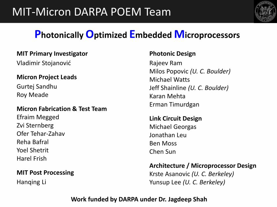
MIT-Micron DARPA POEM Team
MIT Primary Investigator
Vladimir Stojanović
Micron Project Leads
Gurtej Sandhu Roy Meade
Micron Fabrication & Test Team Efraim Megged Zvi Sternberg Ofer Tehar-Zahav Reha Bafral Yoel Shetrit Harel Frish
MIT Post Processing
Hanqing Li
Work funded by DARPA under Dr. Jagdeep Shah
Photonic Design
Rajeev Ram Milos Popovic (U. C. Boulder) Michael Watts Jeff Shainline (U. C. Boulder) Karan Mehta Erman Timurdgan
Link Circuit Design Michael Georgas Jonathan Leu Ben Moss Chen Sun
Architecture / Microprocessor Design Krste Asanovic (U. C. Berkeley) Yunsup Lee (U. C. Berkeley)
Photonically Optimized Embedded Microprocessors
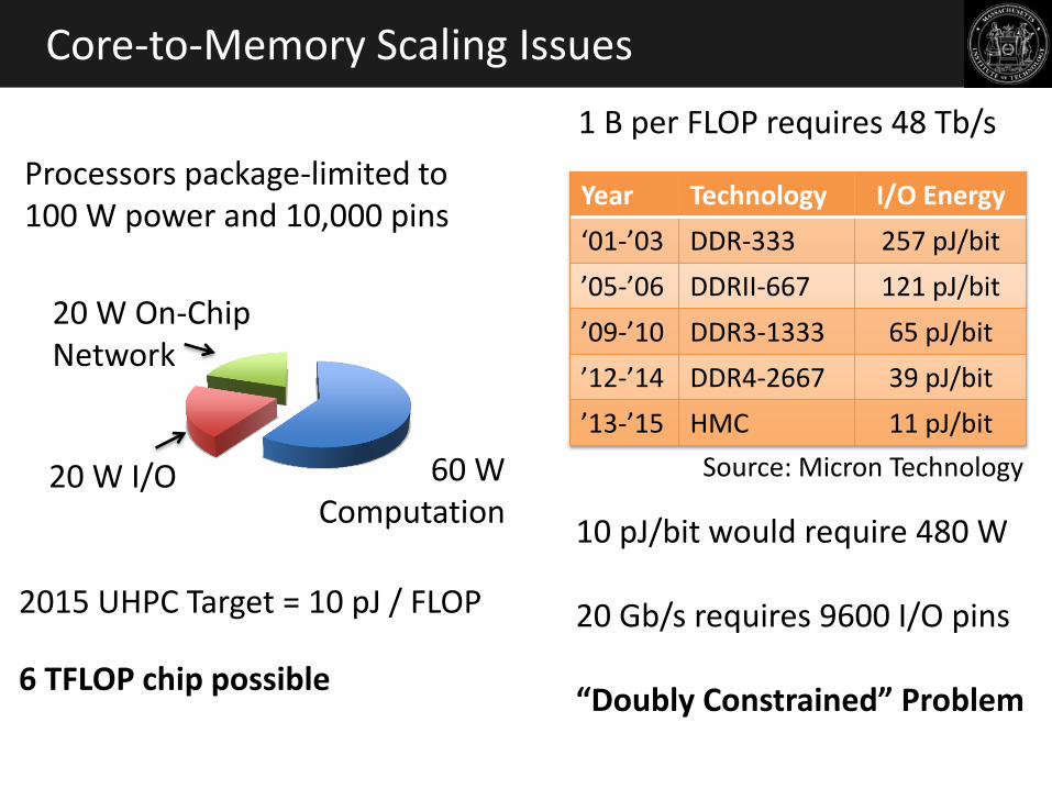
Core-to-Memory Scaling Issues
10 pJ/bit would require 480 W 20 Gb/s requires 9600 I/O pins “Doubly Constrained” Problem
Year Technology I/O Energy
‘01-’03 DDR-333 257 pJ/bit
’05-’06 DDRII-667 121 pJ/bit
’09-’10 DDR3-1333 65 pJ/bit
’12-’14 DDR4-2667 39 pJ/bit
’13-’15 HMC 11 pJ/bit
Processors package-limited to 100 W power and 10,000 pins
60 W Computation
20 W On-Chip Network
20 W I/O
2015 UHPC Target = 10 pJ / FLOP
6 TFLOP chip possible
1 B per FLOP requires 48 Tb/s
Source: Micron Technology
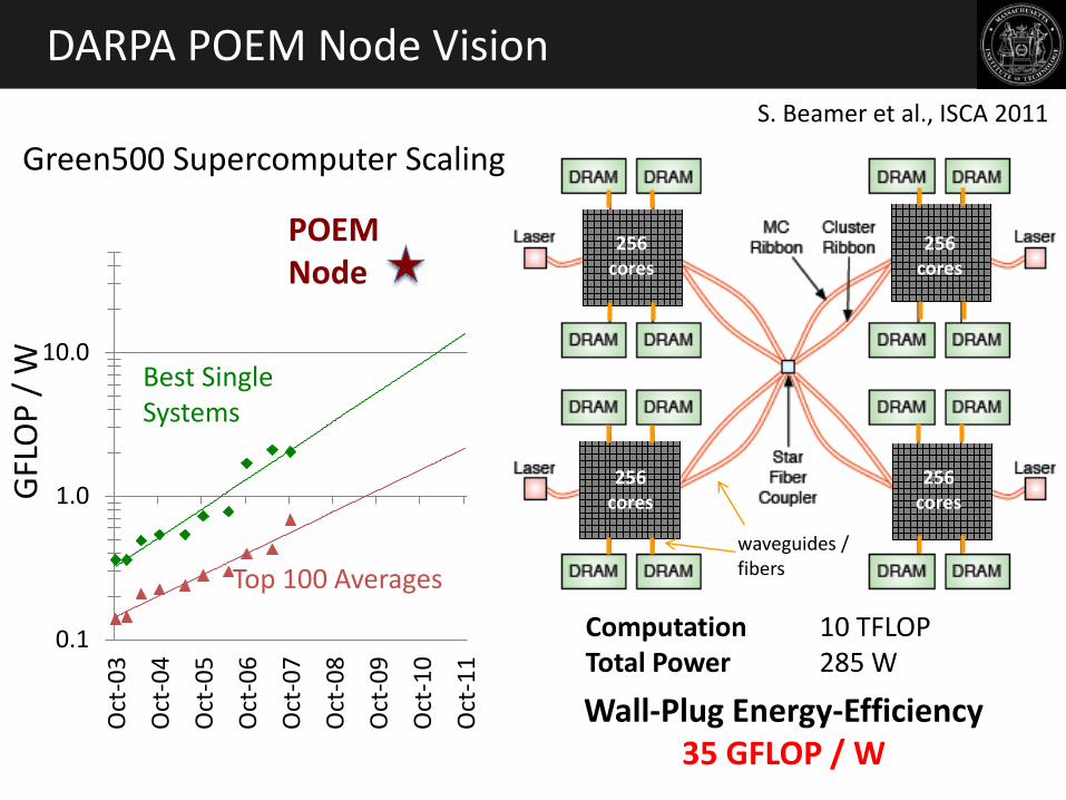
DARPA POEM Node Vision
Computation 10 TFLOP Total Power 285 W
256 cores
256 cores
waveguides / fibers
256 cores
256 cores
Wall-Plug Energy-Efficiency 35 GFLOP / W
0.1
1.0
10.0
Oct
-03
Oct
-04
Oct
-05
Oct
-06
Oct
-07
Oct
-08
Oct
-09
Oct
-10
Oct
-11
GFL
OP
/ W
POEM Node
Green500 Supercomputer Scaling
Best Single Systems
Top 100 Averages
S. Beamer et al., ISCA 2011
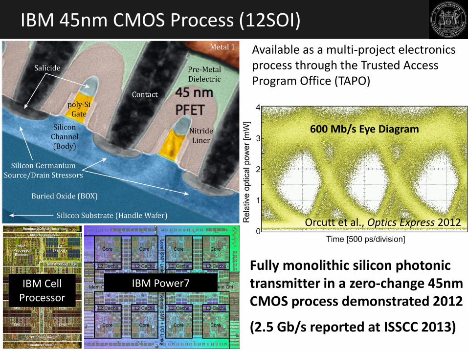
600 Mb/s Eye Diagram
Orcutt et al., Optics Express 2012
Fully monolithic silicon photonic transmitter in a zero-change 45nm CMOS process demonstrated 2012
(2.5 Gb/s reported at ISSCC 2013)
IBM 45nm CMOS Process (12SOI)
IBM Cell Processor
IBM Power7
Available as a multi-project electronics process through the Trusted Access Program Office (TAPO)
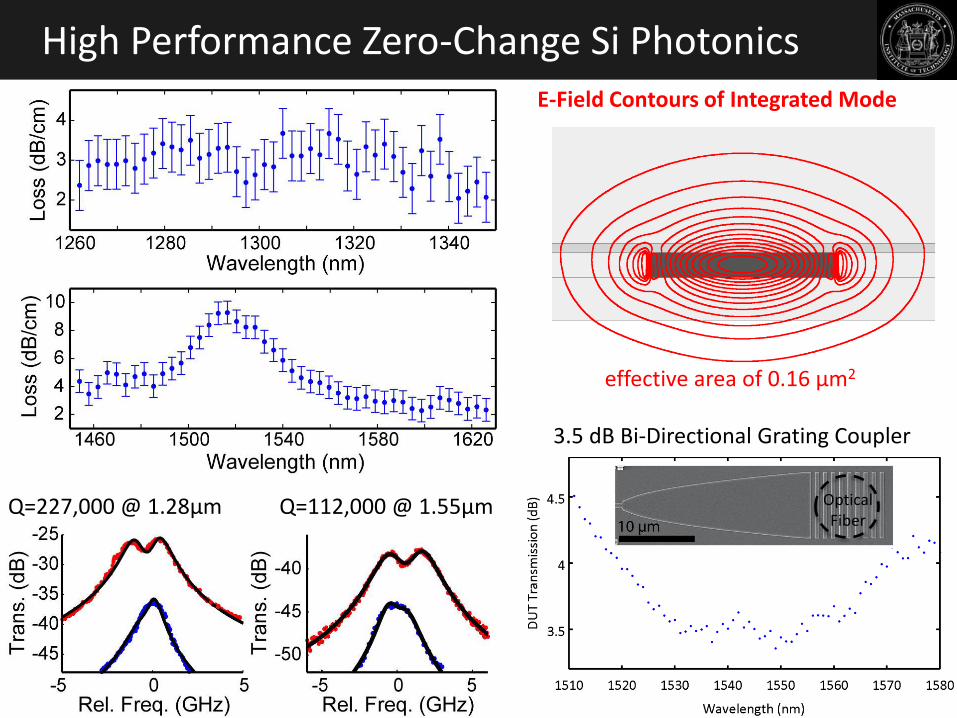
Q=227,000 @ 1.28μm Q=112,000 @ 1.55μm
E-Field Contours of Integrated Mode
effective area of 0.16 μm2
Optical Fiber
3.5 dB Bi-Directional Grating Coupler
High Performance Zero-Change Si Photonics
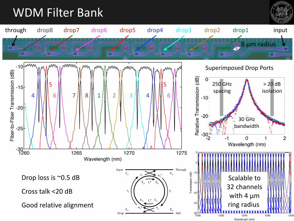
WDM Filter Bank 22
8 7 6
5
4 1 2 3 4
5
6
through input drop8 drop7 drop6 drop5 drop4 drop3 drop2 drop1
> 20 dB isolation
30 GHz bandwidth
250 GHz spacing
Superimposed Drop Ports
Drop loss is ~0.5 dB
Cross talk <20 dB
Good relative alignment
Scalable to 32 channels with 4 μm ring radius
8 μm radius
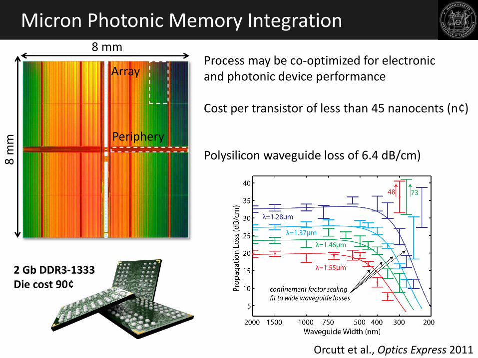
Micron Photonic Memory Integration
2 Gb DDR3-1333 Die cost 90¢
Array
Periphery
8 mm
8 m
m
Process may be co-optimized for electronic and photonic device performance
Cost per transistor of less than 45 nanocents (n¢)
Polysilicon waveguide loss of 6.4 dB/cm)
Orcutt et al., Optics Express 2011
1. Process Integration
2. Area
3. Energy Efficiency
4. Alternative Schemes
Monolithic Front-End Photonics
CMOS
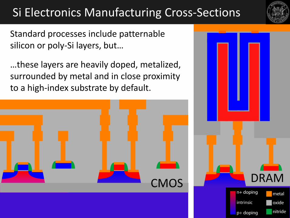
Si Electronics Manufacturing Cross-Sections
DRAM Cross-Section
DRAM
Standard processes include patternable silicon or poly-Si layers, but…
…these layers are heavily doped, metalized, surrounded by metal and in close proximity to a high-index substrate by default.
<150 nm SiO2
Silicon Substrate
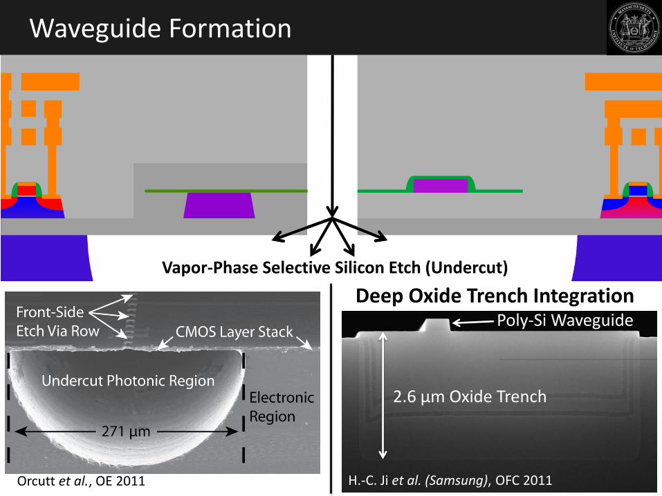
Waveguide Formation
Deep Oxide Trench Integration
H.-C. Ji et al. (Samsung), OFC 2011
2.6 μm Oxide Trench
Poly-Si Waveguide
Orcutt et al., OE 2011
Vapor-Phase Selective Silicon Etch (Undercut)
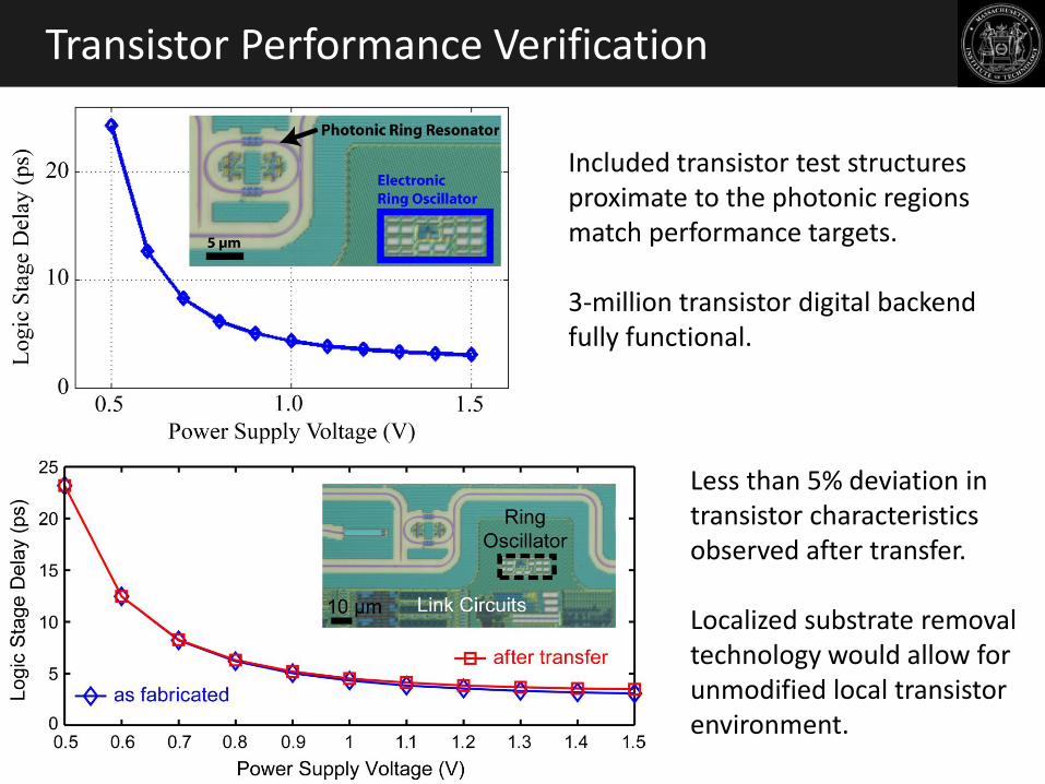
Transistor Performance Verification 14
Included transistor test structures proximate to the photonic regions match performance targets. 3-million transistor digital backend fully functional.
Less than 5% deviation in transistor characteristics observed after transfer. Localized substrate removal technology would allow for unmodified local transistor environment.
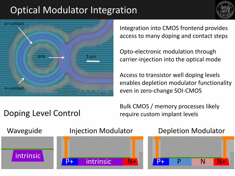
Optical Modulator Integration 24
Integration into CMOS frontend provides access to many doping and contact steps Opto-electronic modulation through carrier-injection into the optical mode Access to transistor well doping levels enables depletion modulator functionality even in zero-change SOI-CMOS Bulk CMOS / memory processes likely require custom implant levels
5 μm poly
p+ contact
n+ contact
intrinsic intrinsic N+ P+ P+ P N+ N
Waveguide Injection Modulator Depletion Modulator
Doping Level Control
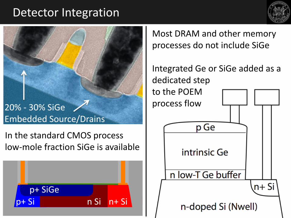
Detector Integration
p+ Si n Si n+ Si
p+ SiGe
Most DRAM and other memory processes do not include SiGe Integrated Ge or SiGe added as a dedicated step to the POEM process flow 20% - 30% SiGe
Embedded Source/Drains
In the standard CMOS process low-mole fraction SiGe is available
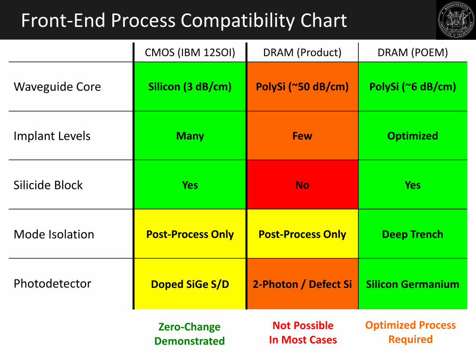
Front-End Process Compatibility Chart
CMOS (IBM 12SOI) DRAM (Product) DRAM (POEM)
Waveguide Core
Silicon (3 dB/cm) PolySi (~50 dB/cm) PolySi (~6 dB/cm)
Implant Levels
Many Few Optimized
Silicide Block
Yes No Yes
Mode Isolation
Post-Process Only Post-Process Only Deep Trench
Photodetector
Doped SiGe S/D 2-Photon / Defect Si Silicon Germanium
Zero-Change Demonstrated
Not Possible In Most Cases
Optimized Process Required
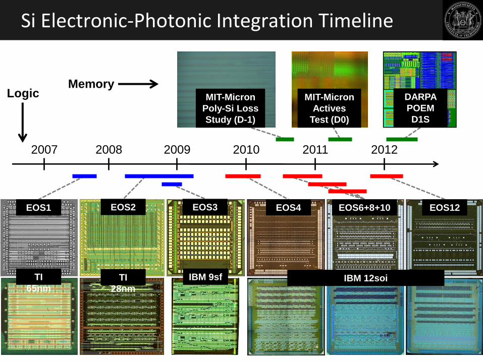
Si Electronic-Photonic Integration Timeline 14
IBM 9sf TI
28nm
TI
65nm
EOS1 EOS2 EOS3 EOS4 EOS6+8+10
2007 2008 2009 2010 2011 2012
IBM 12soi
EOS12
MIT-Micron
Poly-Si Loss
Study (D-1)
MIT-Micron
Actives
Test (D0)
DARPA
POEM
D1S
Memory Logic
1. Process Integration
2. Area
3. Energy Efficiency
4. Alternative Schemes
Monolithic Front-End Photonics
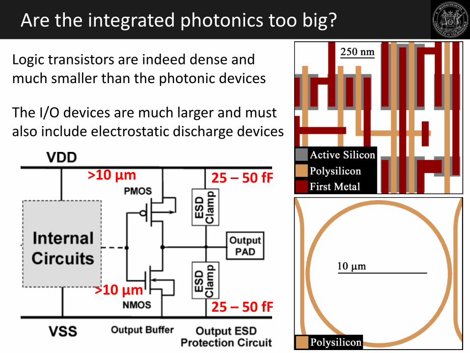
Are the integrated photonics too big?
Logic transistors are indeed dense and much smaller than the photonic devices
The I/O devices are much larger and must also include electrostatic discharge devices
25 – 50 fF
25 – 50 fF
>10 μm
>10 μm
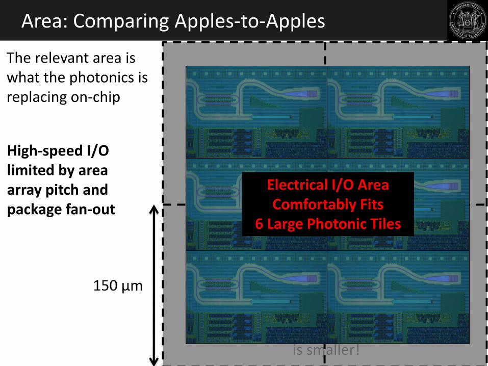
Area: Comparing Apples-to-Apples
100 μm
120 μm
Photonic I/O tile with injection driver and R=10μm modulator
is smaller!
Driver
I/O Mod.
The relevant area is what the photonics is replacing on-chip Low speed digital I/O
tile from our chips (ARM provided IP)
High-speed I/O limited by area array pitch and package fan-out
150 μm
Vdd
Gnd
High Speed I/O +
High Speed I/O –
Electrical I/O Area Comfortably Fits
6 Large Photonic Tiles
1. Process Integration
2. Area
3. Energy Efficiency
4. Alternative Schemes
Monolithic Front-End Photonics
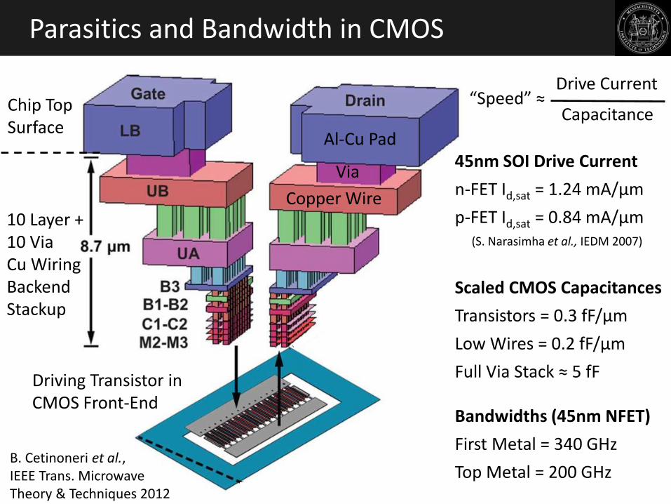
Parasitics and Bandwidth in CMOS
B. Cetinoneri et al., IEEE Trans. Microwave Theory & Techniques 2012
Driving Transistor in CMOS Front-End
10 Layer + 10 Via Cu Wiring Backend Stackup
Chip Top Surface
Al-Cu Pad
Copper Wire
Via
“Speed” ≈ Drive Current
Capacitance
45nm SOI Drive Current
n-FET Id,sat = 1.24 mA/μm
p-FET Id,sat = 0.84 mA/μm (S. Narasimha et al., IEDM 2007)
Scaled CMOS Capacitances
Transistors = 0.3 fF/μm
Low Wires = 0.2 fF/μm
Full Via Stack ≈ 5 fF
Bandwidths (45nm NFET)
First Metal = 340 GHz
Top Metal = 200 GHz
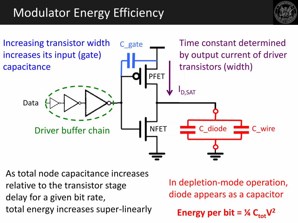
Modulator Energy Efficiency
Data
NFET
PFET
Driver buffer chain
As total node capacitance increases relative to the transistor stage delay for a given bit rate, total energy increases super-linearly
In depletion-mode operation, diode appears as a capacitor
C_wire C_diode
Energy per bit = ¼ CtotV2
C_gate Increasing transistor width increases its input (gate) capacitance
Time constant determined by output current of driver transistors (width)
ID,SAT
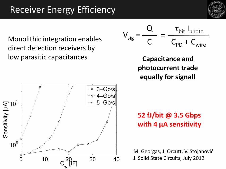
Receiver Energy Efficiency
Monolithic integration enables direct detection receivers by low parasitic capacitances
M. Georgas, J. Orcutt, V. Stojanović J. Solid State Circuits, July 2012
52 fJ/bit @ 3.5 Gbps with 4 μA sensitivity
Vsig = Q
C
τbit Iphoto
CPD + Cwire
=
Capacitance and photocurrent trade equally for signal!
1. Process Integration
2. Area
3. Energy Efficiency
4. Alternative Schemes
Monolithic Front-End Photonics
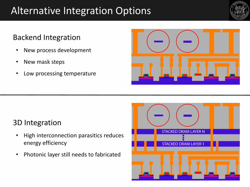
Alternative Integration Options
3D Integration
• High interconnection parasitics reduces energy efficiency
• Photonic layer still needs to fabricated
Backend Integration
• New process development
• New mask steps
• Low processing temperature
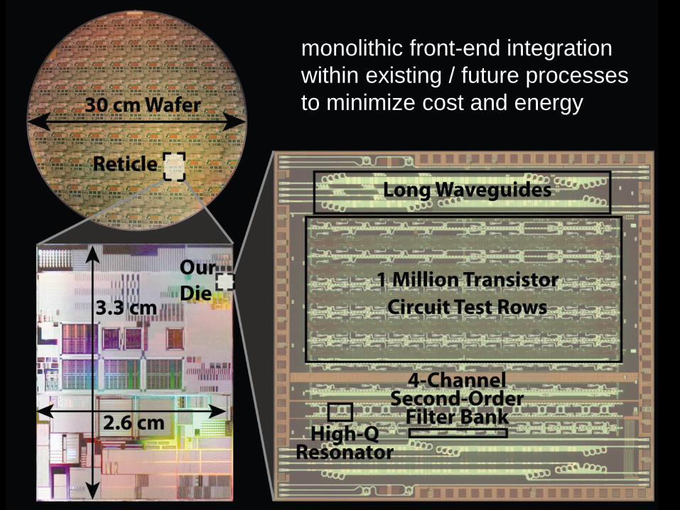
monolithic front-end integration
within existing / future processes
to minimize cost and energy
Process compliant integration enables monolithic photonics in scaled CMOS / DRAM products
Monolithic photonics can provide an area advantage for microprocessors
Energy efficiency may be optimized by front-end photonic integration
Conclusions

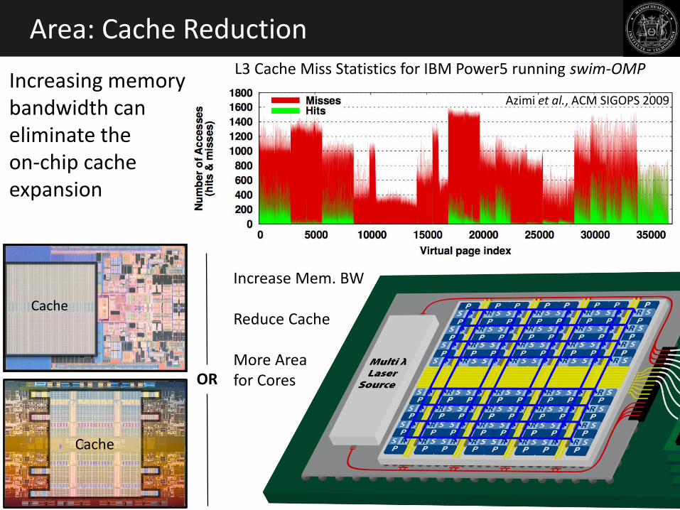
Azimi et al., ACM SIGOPS 2009
Area: Cache Reduction
Cache
L3 Cache Miss Statistics for IBM Power5 running swim-OMP Increasing memory bandwidth can eliminate the on-chip cache expansion
OR
Increase Mem. BW Reduce Cache More Area for Cores
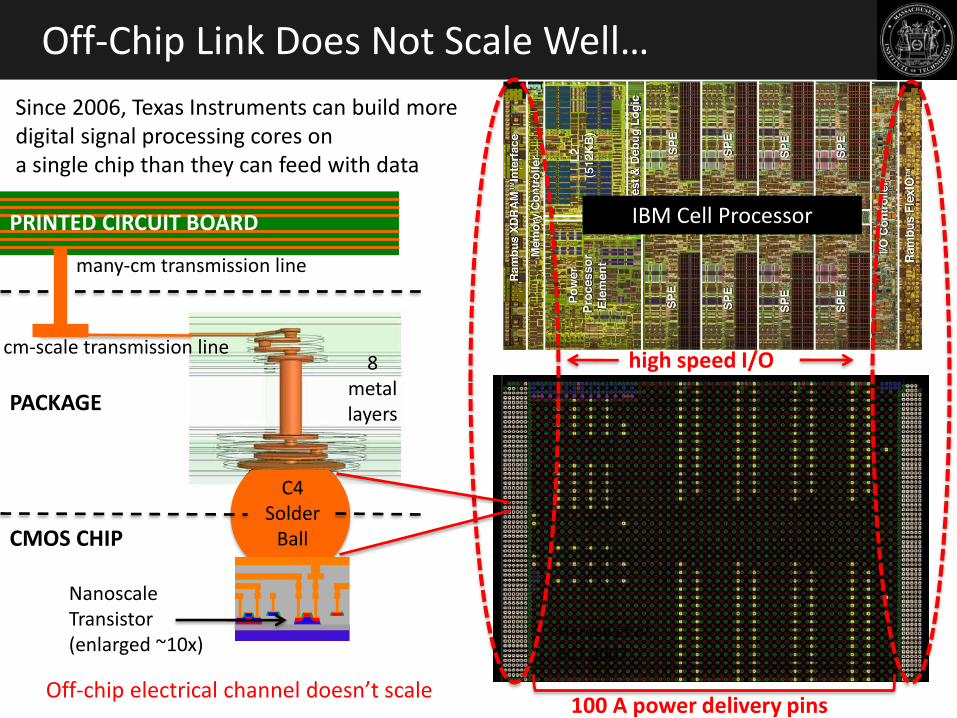
IBM Cell Processor
Harvey et al., ECT 2007
Off-Chip Link Does Not Scale Well…
Since 2006, Texas Instruments can build more digital signal processing cores on a single chip than they can feed with data
high speed I/O
100 A power delivery pins Off-chip electrical channel doesn’t scale
Nanoscale Transistor (enlarged ~10x)
C4 Solder
Ball CMOS CHIP
PRINTED CIRCUIT BOARD
PACKAGE
8 metal layers
many-cm transmission line
cm-scale transmission line