integrating asynchronous digital design into the ... the increasing difficulty of clock...
TRANSCRIPT

Proceedings of the 2006 Midwest Section Conference of the American Society for Engineering Education
Integrating Asynchronous Digital Design into the Undergraduate Computer Engineering Curriculum
Scott C. Smith
University of Missouri – Rolla Department of Electrical and Computer Engineering
133 Emerson Electric Co. Hall, 1870 Miner Circle, Rolla, MO 65409 Phone: (573) 341-4232, Fax: (573) 341-4532, E-mail: [email protected]
Website: www.ece.umr.edu/~smithsco Abstract The development of synchronous circuits currently dominates the semiconductor design industry. However, there are major limiting factors to the synchronous, clocked approach, including the increasing difficulty of clock distribution, increasing clock rates, decreasing feature size, increasing power consumption, timing closure effort, and difficulty with design reuse. Asynchronous (clockless) circuits require less power, generate less noise, produce less electro-magnetic interference (EMI), and allow for easier reuse of components, compared to their synchronous counterparts, without compromising performance. As the demand continues for designs with higher performance, higher complexity, and decreased feature size, asynchronous paradigms will become more widely used in the industry, as evidenced by the International Technology Roadmap for Semiconductors’ (ITRS) prediction of a likely shift from synchronous to asynchronous design styles in order to increase circuit robustness, decrease power, and alleviate many clock-related issues. ITRS predicts that asynchronous circuits will account for 19% of chip area within the next 5 years, and 30% of chip area within the next 10 years. 1. Introduction To meet this growing industry need, students in Computer Engineering should be introduced to asynchronous design to make them more marketable and more prepared for the challenges faced by the digital design community for years to come. In most Computer Engineering curriculums students are only taught the synchronous, clocked paradigm and never even touch on asynchronous digital design. Those curriculums that do mention asynchronous design do so only in passing; the students are not taught how to design asynchronous circuits. The widespread introduction of asynchronous digital design in the classroom is largely constrained by the lack of introductory educational material. This paper will present one approach for integrating asynchronous circuit design into the undergraduate Computer Engineering curriculum, focusing on inclusion in a course on Hardware Design Languages (HDLs), such as VHDL. The proposed method utilizes a VHDL library of asynchronous gates, components, and functions, which can be used to design asynchronous circuits of various complexities. The asynchronous topics fit nicely into the discussion of VHDL generate statements.
The author gratefully acknowledges the support from the National Science Foundation under CCLI grant DUE-0536343.

Proceedings of the 2006 Midwest Section Conference of the American Society for Engineering Education
2
This paper is organized into 5 sections. Section 2 presents an overview of asynchronous logic; Section 3 describes the asynchronous materials developed for use in undergraduate Computer Engineering courses; Section 4 depicts the original VHDL course outline and how it has been augmented to include the asynchronous materials; and Section 5 presents the outcomes of the first offering of the VHDL course with the asynchronous materials included and provides conclusions and directions for future work. 2. Overview of Asynchronous Logic Asynchronous circuits can be grouped into two main categories: bounded-delay and delay-insensitive models. Bounded-delay models such as micropipelines 1 assume that delays in both gates and wires are bounded. Delays are added based on worse-case scenarios to avoid hazard conditions. This leads to extensive timing analysis of worse-case behavior to ensure correct circuit operation. On the other hand, delay-insensitive (DI) circuits assume delays in both logic elements and interconnects to be unbounded, although they assume that wire forks within basic components, such as a full adder, are isochronic 2, 3, meaning that the wire delays within a component are much less than the logic element delays within the component, which is a valid assumption even in future nanometer technologies. Wires connecting components do not need to adhere to the isochronic fork assumption. This implies the ability to operate in the presence of indefinite arrival times for the reception of inputs. Completion detection of the output signals allows for handshaking to control input wavefronts. DI design styles therefore require very little, if any, timing analysis to ensure correct operation (i.e. they are correct-by-construction), and they also yield average-case performance rather than the worse-case performance of bounded-delay and synchronous paradigms 4.
2.1 Delay-Insensitive Circuits Most DI methods combine C-elements 5 with Boolean gates for circuit construction. A C-element behaves as follows: when all inputs assume the same value then the output assumes this value, otherwise the output does not change. Seitz’s 6, DIMS 7, Anantharaman’s 8, Singh’s 9, and David’s 10 methods are examples of DI paradigms that only use C-elements to achieve delay-insensitivity. On the other hand, both Phased Logic 11 and NULL Convention Logic (NCL) 12 target a library of multiple gates with hysteresis state-holding functionality. Phased Logic converts a traditional synchronous gate-level circuit into a delay-insensitive circuit by replacing each conventional synchronous gate with its corresponding Phased Logic gate, and then augmenting the new network with additional signals 11. NCL functions are realized using 27 fundamental gates implementing the set of all functions of four or fewer variables, each with hysteresis state-holding functionality 13. Seitz’s method, Anantharaman’s approach, and DIMS require the generation of all minterms to implement a function, where a minterm is defined as the logical AND, or product, containing all input signals in either complemented or non-complemented form. While Singh’s and David’s methods do not require full minterm generation, they rely solely on C-elements for speed-independence. NCL also does not require full minterm generation and furthermore includes 27 fundamental state-holding gates for circuit design, rather than only C-elements, thus yielding a greater potential for optimization than other delay-insensitive paradigms 14. Phased Logic does not require full minterm generation and does not rely solely on C-elements for speed-

Proceedings of the 2006 Midwest Section Conference of the American Society for Engineering Education
3
independence; however Phased Logic circuitry is derived directly from its equivalent synchronous design, and not created independently; thus it does not have the same potential for optimization as does NCL. Furthermore, the Phased Logic paradigm has been developed mainly for easing the timing constraints of synchronous designs, not for obtaining speed and power benefits 11, whereas these are main concerns of other asynchronous paradigms. Self-timed circuits can also be designed at the transistor level as demonstrated by Martin 15. However, automation of this method would be vastly different than that of the standard synchronous approach, since it optimizes designs at the transistor level instead of targeting a predefined set of gates, as do the previously mentioned DI methods. Overall, NULL Convention Logic offers the best opportunity for integrating asynchronous digital design into the predominantly synchronous semiconductor design industry for the following reasons: 1) The framework for NCL systems consist of DI combinational logic sandwiched between DI
registers, as shown in Figure 1. This framework is very similar to synchronous systems, such that the automated design of NCL circuits can follow the same fundamental steps as synchronous circuit design automation. This will enable the developed DI design flow to be more easily incorporated into the chip design industry, since the tools and design process will already be familiar to designers, such that the learning curve is relatively flat;
2) NCL systems are delay-insensitive, making the design process much easier to automate than other non-DI asynchronous paradigms, since minimal delay analysis is necessary to ensure correct circuit operation; and
3) NCL systems have power, noise, and EMI advantages compared to synchronous circuits, performance and design reuse advantages compared to synchronous and non-DI asynchronous paradigms, area and performance advantages compared to other DI paradigms, and have a number of advantages for designing complex systems, like SoCs, including substantially reduced crosstalk between analog and digital circuits, ease of integrating multi-rate circuits, and ease of component reuse and technology migration.
DI Register
KiKo
DICombinational
Logic
DI Register
KiKo
CompletionDetection
DICombinational
Logic
DI Register
KiKo
CompletionDetection
DI Register
KiKo
Figure 1. NCL system framework: input wavefronts are controlled by local handshaking signals and Completion Detection instead of by a global clock signal. Feedback requires at least three DI registers in the feedback loop to prevent deadlock 16.
2.2 NCL Circuits NCL circuits utilize dual-rail or quad-rail logic to achieve delay-insensitivity. A dual-rail signal, D, consists of two wires, D0 and D1, which may assume any value from the set {DATA0, DATA1, NULL}. The DATA0 state (D0 = 1, D1 = 0) corresponds to a Boolean logic 0, the DATA1 state (D0 = 0, D1 = 1) corresponds to a Boolean logic 1, and the NULL state (D0 = 0, D1 = 0) corresponds to the empty set meaning that the value of D is not yet available. The two rails are mutually exclusive, such that both rails can never be asserted simultaneously; this state

Proceedings of the 2006 Midwest Section Conference of the American Society for Engineering Education
4
is defined as an illegal state. A quad-rail signal, Q, consists of four wires, Q0, Q1, Q2, and Q3, which may assume any value from the set {DATA0, DATA1, DATA2, DATA3, NULL}. The DATA0 state (Q0 = 1, Q1 = 0, Q2 = 0, Q3 = 0) corresponds to two Boolean logic signals, X and Y, where X = 0 and Y = 0. The DATA1 state (Q0 = 0, Q1 = 1, Q2 = 0, Q3 = 0) corresponds to X = 0 and Y = 1. The DATA2 state (Q0 = 0, Q1 = 0, Q2 = 1, Q3 = 0) corresponds to X = 1 and Y = 0. The DATA3 state (Q0 = 0, Q1 = 0, Q2 = 0, Q3 = 1) corresponds to X = 1 and Y = 1, and the NULL state (Q0 = 0, Q1 = 0, Q2 = 0, Q3 = 0) corresponds to the empty set meaning that the result is not yet available. The four rails of a quad-rail NCL signal are mutually exclusive, such that no two rails can ever be asserted simultaneously; these states are defined as illegal states. Both dual-rail and quad-rail signals are space optimal 1-hot delay-insensitive codes, requiring two wires per bit. NCL circuits are comprised of 27 fundamental gates 14. These 27 gates constitute the set of all functions consisting of four or fewer variables. Since each rail of an NCL signal is considered a separate variable, a four variable function is not the same as a function of four literals, which would normally consist of eight variables. The primary type of threshold gate, shown in Figure 2, is the THmn gate, where 1 ≤ m ≤ n. THmn gates have n inputs. At least m of the n inputs must be asserted before the output will become asserted. In a THmn gate, each of the n inputs is connected to the rounded portion of the gate; the output emanates from the pointed end of the gate; and the gate’s threshold value, m, is written inside of the gate. Another type of threshold gate is referred to as a weighted threshold gate, denoted as THmnWw1w2…wR. Weighted threshold gates have an integer value, m ≥ wR > 1, applied to inputR. Here 1 ≤ R < n; where n is the number of inputs; m is the gate’s threshold; and w1, w2, …wR, each > 1, are the integer weights of input1, input2, … inputR, respectively. For example, consider the TH34W2 gate, whose n = 4 inputs are labeled A, B, C, and D, shown in Figure 3. The weight of input A, W(A), is therefore 2. Since the gate’s threshold, m, is 3, this implies that in order for the output to be asserted, either inputs B, C, and D must all be asserted, or input A must be asserted along with any other input, B, C, or D. NCL threshold gates are designed with hysteresis state-holding capability, such that all asserted inputs must be de-asserted before the output will be de-asserted. Hysteresis ensures a complete transition of inputs back to NULL before asserting the output associated with the next wavefront of input data. Therefore, a THnn gate is equivalent to an n-input C-element and a TH1n gate is equivalent to an n-input OR gate. NCL threshold gates may also include a reset input to initialize the output. Circuit diagrams designate resettable gates by either a d or an n appearing inside the gate, along with the gate’s threshold. d denotes the gate as being reset to logic 1; n, to logic 0. These resettable gates are used in the design of DI registers 16.
m
input 1input 2
input n
output
Figure 2. THmn threshold gate. Figure 3. TH34w2 threshold gate: Z = AB + AC + AD + BCD

Proceedings of the 2006 Midwest Section Conference of the American Society for Engineering Education
5
Figure 4 shows a static CMOS implementation of a TH23 gate, with inputs A, B, and C, and output Z. 13 details various design implementations (static, semi-static, and dynamic) of NCL threshold gates. Table I lists the 27 fundamental NCL gates used to construct NCL circuits, along with their corresponding Boolean equations and number of transistors for static CMOS implementation. These 27 macros constitute the set of all functions consisting of four or fewer variables. Twenty four of these macros can be realized using complex threshold gates, identical to the standard threshold gate forms for functions of four or fewer variables 17, 18, 19. The remaining three macros could be constructed from threshold gate networks, but have been implemented as transistor networks to reduce area and delay.
NCL systems contain at least two DI registers, one at both the input and at the output. Two adjacent register stages interact through their request and acknowledge signals, Ki and Ko, respectively, to prevent the current DATA wavefront from overwriting the previous DATA wavefront, by ensuring that the two DATA wavefronts are always separated by a NULL wavefront. The acknowledge signals are combined in the Completion Detection circuitry to produce the request signal(s) to the previous register stage, utilizing either the full-word or bit-wise completion strategy 16. To ensure delay-insensitivity, NCL circuits must adhere to the following criteria: Input-Completeness 14 and Observability 14. Furthermore, when circuits utilize the bit-wise completion strategy with selective input-incomplete components, they must also adhere to the completion-completeness criterion 20, which requires that completion signals only be generated such that no two adjacent DATA wavefronts can interact within any combinational component.
Figure 4. Static CMOS implementation of a TH23 gate: Z = AB + AC + BC.
C
B
A
Z
A
B C
C
B
AA B
C

Proceedings of the 2006 Midwest Section Conference of the American Society for Engineering Education
6
Table 1. 27 fundamental NCL gates.
NCL Macro Boolean Function Transistor Count TH12 A + B 6 TH22 AB 12 TH13 A + B + C 8 TH23 AB + AC + BC 18 TH33 ABC 16 TH23w2 A + BC 14 TH33w2 AB + AC 14 TH14 A + B + C + D 10 TH24 AB + AC + AD + BC + BD + CD 26 TH34 ABC + ABD + ACD + BCD 24 TH44 ABCD 20 TH24w2 A + BC + BD + CD 20 TH34w2 AB + AC + AD + BCD 22 TH44w2 ABC + ABD + ACD 23 TH34w3 A + BCD 18 TH44w3 AB + AC + AD 16 TH24w22 A + B + CD 16 TH34w22 AB + AC + AD + BC + BD 22 TH44w22 AB + ACD + BCD 22 TH54w22 ABC + ABD 18 TH34w32 A + BC + BD 17 TH54w32 AB + ACD 20 TH44w322 AB + AC + AD + BC 20 TH54w322 AB + AC + BCD 21 THxor0 AB + CD 20 THand0 AB + BC + AD 19 TH24comp AC + BC + AD + BD 18
2.3 Asynchronous Circuit Synthesis Several approaches have been proposed for synthesizing asynchronous circuits from high-level specification languages 2, 21, 22, 23, 24, 25; however all of these require the user to learn a new language to describe the asynchronous circuit, such as Balsa 24 or Tangram 22. High-level descriptions cannot be specified with standard HDLs (i.e. VHDL, Verilog, etc.) commonly used for synchronous circuits. The conversion of a synchronous circuit to its Phased-Logic equivalent has been automated 26; however, as mentioned before, Phased-Logic does not provide the same benefits as other DI approaches, since the Phased-Logic implementation is translated directly from the synchronous circuit and not designed independently. DI circuits can also be designed and simulated at the structural/gate level using commercial design tools, such as Mentor Graphics, Synopsys, and Cadence. However, DI circuits cannot currently be specified as dataflow or behavioral descriptions since DI synthesis tools do not exist. The author is currently developing a comprehensive methodology for automated synthesis, optimization, and testing of DI digital circuits, starting from an RTL HDL description and ending with an FPGA configuration or ASIC layout, which is being incorporated into the industry-

Proceedings of the 2006 Midwest Section Conference of the American Society for Engineering Education
7
standard Mentor Graphics, Synopsys, and Cadence toolsets. With this approach, designing DI circuits will follow a very similar process and utilize the same tools as synchronous circuit design, which will expedite the integration of widespread asynchronous circuit usage in the semiconductor industry, thus alleviating many of today’s clock and power related problems. The basic flow, from left to right, of the proposed NCL design automation methodology is shown in Figure 5. It starts with a VHDL description of the system, which is input to the NCL synthesis tool to be converted to an NCL gate-level netlist. The NCL optimization tool is then used to increase performance of the NCL system, which outputs a modified gate-level netlist. The next step is to decide if the circuit is to be implemented as an ASIC, or on the DI FPGA also being developed by the author. If FPGA implementation is chosen, registration is embedded within the combinational logic to reduce area and increase throughput, the gate-level netlist is placed and routed, and an FPGA configuration file is produced, to be downloaded into the DI FPGA. If ASIC implementation is chosen, the NCL DFT tool is used to augment the gate-level netlist in order to make the DI ASIC testable, which outputs another modified gate-level netlist. The rest of the steps to convert the gate-level netlist to a GDSII file for fabrication are exactly the same as for synchronous design, and can use the existing tools without any necessary modifications. However, these steps are much easier than for synchronous design, since a global clock doesn’t need to be distributed across the entire chip, while ensuring minimal clock skew, which requires extensive delay analysis that requires up to 40% of the design effort for large systems. Note that the proposed NCL design flow is fully compatible with other HDL languages, such as Verilog and System C, since these can be converted to VHDL, using existing design tools, prior to initiating the NCL design process.
Figure 5. NCL automated design methodology flowchart.
The two differences between this design flow and the synchronous one are that synthesis and optimization are performed in two steps and are independent of implementation. In the synchronous flow, implementation decision, synthesis, and optimization, are done using one tool (i.e. Leonardo Spectrum for the Mentor Graphics suite). The NCL flow will also use the same single tool for these steps, but they will be executed using three separate Tcl (tool command language) scripts (i.e. one for synthesis, one for optimization, and one for FPGA placement and routing only if FPGA implementation is chosen). This will allow for the synthesis and optimization methods to be developed concurrently, will give the user more control over the synthesis and optimization process, and will allow for hand-designed circuits to use the optimization tool without the synthesis tool and to be implemented directly on the DI FPGA. These three scripts could be combined into one script in the final implementation, if desired.

Proceedings of the 2006 Midwest Section Conference of the American Society for Engineering Education
8
The NCL design methodology is currently being incorporated into the Mentor Graphics toolset using Tcl scripts that call C-programs, which are executed from within existing Mentor tools to run NCL specific synthesis, optimization, and DFT algorithms, using pull-down menus. The Tcl scripts will provide the interface between the industrial toolset and the developed NCL tool, while the C-programs perform the majority of the actual computation. While this approach will have a slightly longer run-time than direct integration within the core design tool algorithms, it has overriding advantages. First, Tcl scripts can be executed from within all three toolsets, allowing the methodology to be easily ported to the Synopsys and Cadence toolsets, requiring only slight modifications on the front and back ends of the Mentor Graphics Tcl scripts. Second, the core design tool algorithms are proprietary and subject to change. Thus, development of the algorithms as C-programs called by Tcl scripts, and making them publicly available, will allow other researchers to use and modify the tools for continuing enhancement of research in this area. Finally, the developed tools can be readily merged into the core design tool algorithms at a later date for increased run-time performance, if desired. 3. Developed Materials To effectively introduce asynchronous digital design into the computer engineering curriculum, lecture notes, example problems, a group project, and a VHDL library of asynchronous gates, components, and functions were developed for incorporation into a senior-level elective / graduate-level course on Digital System Modeling with VHDL. The lecture notes included discussion of both bounded-delay and delay-insensitive asynchronous paradigms, highlighting the differences between the two and comparing each to the synchronous, clocked paradigm, as overviewed in Section 2.1. Following this general discussion, one specific asynchronous paradigm, NULL Convention Logic (NCL), was studied in detail. This included a general introduction to NCL, as overviewed in Section 2.2, as well as specific presentations and assignments on the fundamental NCL components (i.e. registration, combinational logic, and completion detection), input-completeness and observability, dual-rail combinational circuit design, and pipelining optimization, as detailed below. 3.1 NCL Components NCL systems consist of registration, combinational logic, and completion detection, connected together as shown in Figure 1. NCL registration is realized through cascaded arrangements of single-bit dual-rail registers or single-signal quad-rail registers, depicted in Figures 6 and 7, respectively. These registers consist of TH22 gates that pass a DATA value at the input only when Ki is request for data (rfd) (i.e. logic 1) and likewise pass NULL only when Ki is request for null (rfn) (i.e. logic 0). They also contain a NOR gate to generate Ko, which is rfn when the register output is DATA and rfd when the register output is NULL. The registers shown below are reset to NULL, since all TH22 gates are reset to logic 0. However, either register could be instead reset to a DATA value by replacing exactly one of the TH22n gates with a TH22d gate. An N-bit register stage, comprised of N single-bit dual-rail NCL registers, requires N completion signals, one for each bit. The NCL completion component, shown in Figure 8, uses these N Ko lines to detect complete DATA and NULL sets at the output of every register stage and request the next NULL and DATA set, respectively. In full-word completion, the single-bit output of the

Proceedings of the 2006 Midwest Section Conference of the American Society for Engineering Education
9
completion component is connected to all Ki lines of the previous register stage. Since the maximum input threshold gate is the TH44 gate, the number of logic levels in the completion component for an N-bit register is given by log4 N. Likewise, the completion component for an N-bit quad-rail registration stage requires 2
N inputs, and can be realized in a similar fashion using TH44 gates.
2n
2n
I0
I1
2nI2
I3
O0
O1
O2
O32n
1Ko
Ki
Reset
2n
2n
I0
I1
O0
O1
1Ko
KiReset
Figure 6. Single-bit dual-rail register.
Figure 7. Single-signal quad-rail register.
Ko(1)Ko(2)Ko(3)Ko(4)
Ko(N-3)Ko(N-2)Ko(N-1)
Ko(N)
4
4
4 4Ko(N-7)Ko(N-6)Ko(N-5)Ko(N-4)
4
4
Ko(5)Ko(6)Ko(7)Ko(8)
4 Ko
Figure 8. N-bit completion component.
Proceedings of the 2006 Midwest Section Conference of the American Society for Engineering Education
10
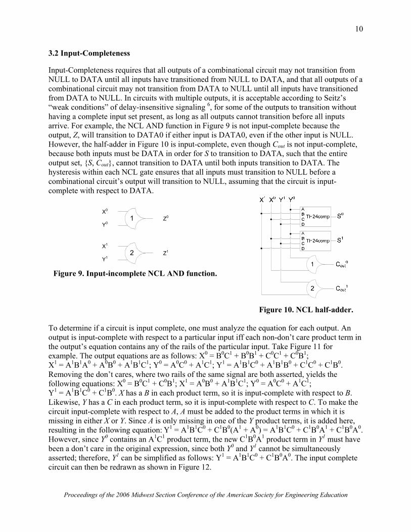
3.2 Input-Completeness Input-Completeness requires that all outputs of a combinational circuit may not transition from NULL to DATA until all inputs have transitioned from NULL to DATA, and that all outputs of a combinational circuit may not transition from DATA to NULL until all inputs have transitioned from DATA to NULL. In circuits with multiple outputs, it is acceptable according to Seitz’s “weak conditions” of delay-insensitive signaling 6, for some of the outputs to transition without having a complete input set present, as long as all outputs cannot transition before all inputs arrive. For example, the NCL AND function in Figure 9 is not input-complete because the output, Z, will transition to DATA0 if either input is DATA0, even if the other input is NULL. However, the half-adder in Figure 10 is input-complete, even though Cout is not input-complete, because both inputs must be DATA in order for S to transition to DATA, such that the entire output set, {S, Cout}, cannot transition to DATA until both inputs transition to DATA. The hysteresis within each NCL gate ensures that all inputs must transition to NULL before a combinational circuit’s output will transition to NULL, assuming that the circuit is input-complete with respect to DATA.
To determine if a circuit is input complete, one must analyze the equation for each output. An output is input-complete with respect to a particular input iff each non-don’t care product term in the output’s equation contains any of the rails of the particular input. Take Figure 11 for example. The output equations are as follows: X0 = B0C1 + B0B1 + C0C1 + C0B1; X1 = A1B1A0 + A0B0 + A1B1C1; Y0 = A0C0 + A1C1; Y1 = A1B1C0 + A1B1B0 + C1C0 + C1B0. Removing the don’t cares, where two rails of the same signal are both asserted, yields the following equations: X0 = B0C1 + C0B1; X1 = A0B0 + A1B1C1; Y0 = A0C0 + A1C1; Y1 = A1B1C0 + C1B0. X has a B in each product term, so it is input-complete with respect to B. Likewise, Y has a C in each product term, so it is input-complete with respect to C. To make the circuit input-complete with respect to A, A must be added to the product terms in which it is missing in either X or Y. Since A is only missing in one of the Y product terms, it is added here, resulting in the following equation: Y1 = A1B1C0 + C1B0(A1 + A0) = A1B1C0 + C1B0A1 + C1B0A0. However, since Y0 contains an A1C1 product term, the new C1B0A1 product term in Y1 must have been a don’t care in the original expression, since both Y0 and Y1 cannot be simultaneously asserted; therefore, Y1 can be simplified as follows: Y1 = A1B1C0 + C1B0A0. The input complete circuit can then be redrawn as shown in Figure 12.
2
1X0
Z1
Z0
Y1
X1
Y0
Figure 10. NCL half-adder.
Figure 9. Input-incomplete NCL AND function.

Proceedings of the 2006 Midwest Section Conference of the American Society for Engineering Education
11
A1 A0 B1 B0 C1 C0
2
X0
Y1
Y0
X1AND0AB
DC
XOR0AB
DC
24compAB
DC
24compAB
DC
3
A1 A0 B1 B0 C1 C0
2
X0
Y0
X1AND0AB
DC
XOR0AB
DC
24compAB
DC
2 Y1
Figure 11. NCL circuit that’s input- Figure 12. Input-complete NCL circuit. incomplete with respect to A. 3.3 Observability Observability requires that no orphans may propagate through a gate 27. An orphan is defined as a wire that transitions during the current DATA wavefront, but is not used in the determination of the output. Orphans are caused by wire forks and can be neglected through the isochronic fork assumption 2, 3, as long as they are not allowed to cross a gate boundary. This observability condition, also referred to as indicatability or stability, ensures that every gate transition is observable at the output; which means that every gate that transitions is necessary to transition at least one of the outputs. Consider an unobservable version of an XOR function, shown in Figure 13, where an orphan is allowed to pass through the TH12 gate. For instance, when X = DATA0 and Y = DATA0, the TH12 gate is asserted, but does not take part in the determination of the output, Z = DATA0. This orphan path is shown in boldface in Figure 13. The equation for Z1 can be repartitioned to obtain a fully observable version of the XOR function, as shown in Figure 14. Here, the two internal TH22 gates are connected to a TH23W2 output gate with a weight of 2, which is the same as the threshold, such that if either internal gate is asserted, it’s corresponding output gate will always become asserted. Note that this circuit is for example only, since the XOR function can be simplified to two TH24comp gates.
2
X0
X1
Y0
Y1
1 3 Z1
2 Z0
2
X0
X1
Y0
Y1
2 2 Z1
2 Z0
Figure 13. Unobservable NCL XOR function. Figure 14. Observable NCL XOR function.

Proceedings of the 2006 Midwest Section Conference of the American Society for Engineering Education
12
The best way to ensure that a circuit is observable is to not divide product terms when mapping equations to their corresponding gate-level circuits. This however is not required for a circuit to be observable, and is not always possible, for example when a product term contains more than four variables. The circuit in Figure 12 is observable even though a product term has been divided. The TH33 gate is observable because its output has the same weight as the output gate’s threshold, similar to the previous example. This is not the case for the TH22 gate, so it must be analyzed more closely. The equation for the TH22 gate is A1B1; and its output is used in the X1 and Y1 product terms: A1B1C1 and A1B1C0, respectively. Therefore, if the TH22 gate is asserted, it will always cause either X1 or Y1 to become asserted because C must either be 0 or 1; hence the TH22 gate is observable. 3.4 Dual-Rail Combinational Circuit Design The design process for NCL combinational circuits is similar to Boolean circuits, where a Karnaugh map, or other simplification technique, can be utilized to determine the simplified sum-of-product (SOP) expressions for each output. However, SOP expressions for both the function’s 1 and 0 outputs are needed. The 0s refer to a signal’s rail0 and the 1s refer to a signal’s rail1. After the expressions for the outputs have been obtained, an assessment must be made to ensure that the circuit is input-complete, as discussed in Section 3.2. If not, the missing input(s) must be added to the appropriate product term(s). The output equations must then be partitioned into groups of four or fewer variables to be mapped to the 27 NCL gates, while ensuring the observability of the circuit, as discussed in the previous section.
000
10
11
01
00 101101
MR2 MR1
MR0 MDi-1
0
0 0 0
000
1
1 1 1
1111
Take for example the design of a partial product (PP) generating component for the most significant bit of a Booth2 multiplier, which is only required to be input-complete with respect to input, MR1. Figure 15 shows the Karnaugh map for this component, along with the optimal coverings. Since this design must be input-complete with respect to MR1, the coverings should not eliminate MR1 from the corresponding product term; hence some of the coverings are 2-coverings instead of 4-coverings. The SOP equations are derived directly form the K-map
Figure 15. K-map for Booth2 PP generation component.
Figure 16. NCL Booth2 PP generation circuit.

Proceedings of the 2006 Midwest Section Conference of the American Society for Engineering Education
13
coverings as follows: PP1 = MR2
1MR11 + MR1
1MR01MDi-1
1 + MR21MR1
0MR01 + MR2
1MR10MDi-1
0; PP0 = MR2
0MR10 + MR1
0MR00MDi-1
1 + MR20MR1
1MR00 + MR2
0MR11MDi-1
0. Since each product term contains MR1, the circuit is input-complete with respect to MR1. The equations can be partitioned into four groups of 4 variables as highlighted above, resulting in the optimized circuit shown in Figure 16. Since no product terms were divided, the circuit is observable. 3.5 NCL Pipelining Optimization NCL systems can be optimized for speed by partitioning the combinational circuitry and inserting additional NCL registers and corresponding completion components. However, NCL circuits cannot be partitioned arbitrarily; they can only be divided at component boundaries in order to preserve delay-insensitivity. The cycle time for an NCL system, TDD, can be estimated as the worse-case stage delay of any stage in the pipeline, where the delay of one stage is equal to twice the sum of the stage’s worse-case combinational delay and its completion delay, to account for both the DATA and NULL wavefronts 16. Algorithm 1 depicts this calculation for an N-stage pipeline, where Dcombi and Dcompi are stagei’s combinational and completion delays, respectively. max_delay = 2 × (Dcomb1 + Dcomp1)
for (i = 2 to N) loop temp_delay = 2 × (Dcombi + Dcompi) if (temp_delay > max_delay) then max_delay = temp_delay end if end loop worst_case_throughput = 1 / max_delay
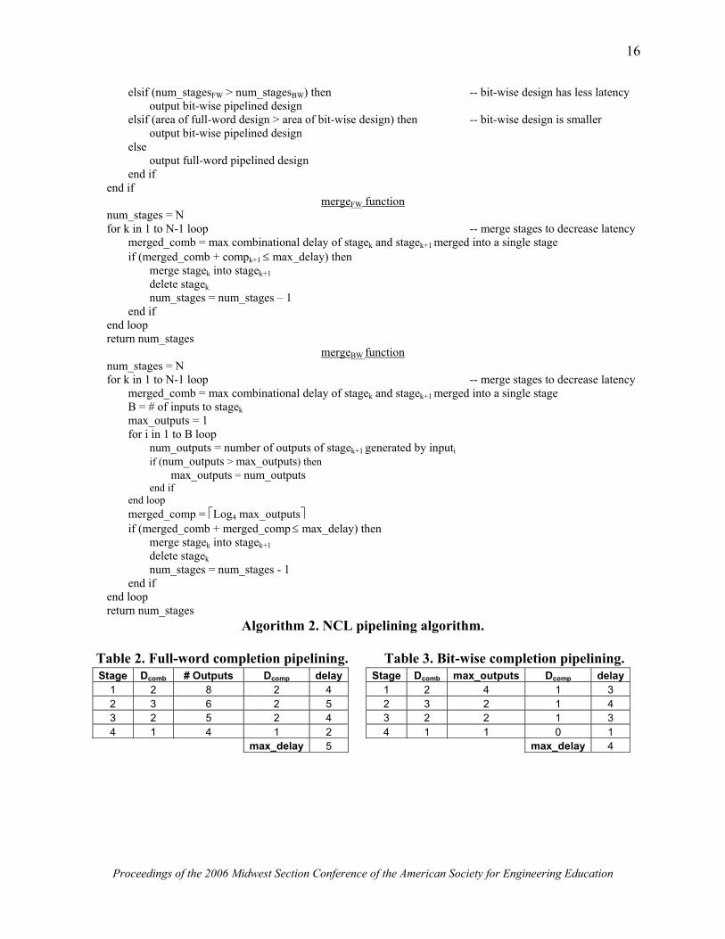
Algorithm 1. NCL throughput calculation. NCL pipelining can utilize either of two completion strategies: full-word or bit-wise completion. Full-word completion, as shown in Figure 17, requires that the acknowledge signals from each bit in registeri be conjoined together by the completion component, whose single-bit output is connected to all request lines of registeri-1. On the other hand, bit-wise completion, as shown in Figure 18, only sends the completion signal from bit b in registeri back to the bits in registeri-1 that took part in the calculation of bit b. This method may therefore require fewer logic levels than that of full-word completion, thus increasing throughput 16. In this example, bit-wise completion is faster, but it requires more area.

Proceedings of the 2006 Midwest Section Conference of the American Society for Engineering Education
14
NCL Completion
X(3) X(2) X(1) X(0)
NCLRegister
A(5) A(0)A(1)A(2)A(3)A(4)
Ki
NCLRegister
NCLRegister
NCLRegister
Ko
Ki
Ko
Ki
Ko
Ki
Ko
NCLRegisterKi
NCLRegister
NCLRegister
NCLRegister
Ko
Ki
Ko
Ki
Ko
Ki
KoNCLRegisterKi
KoNCLRegisterKi
Ko
Ki
NCL Completion
Ko Reset
4
43
Figure 17. Full-word completion.
Figure 18. Bit-wise completion.
NCL Completion
X(3) X(2) X(1) X(0)
NCLRegister
A(5) A(0)A(1)A(2)A(3)A(4)
Ki
NCLRegister
NCLRegister
NCLRegister
Ko
Ki
Ko
Ki
Ko
Ki
Ko
NCLRegisterKi
NCLRegister
NCLRegister
NCLRegister
Ko
Ki
Ko
Ki
Ko
Ki
KoNCLRegisterKi
KoNCLRegisterKi
Ko
Ki(5)
Ko(3) Reset
3
NCL Completion NCL CompletionNCL Completion
Ki(4) Ki(3) Ki(2) Ki(1) Ki(0)
Ko(2) Ko(1) Ko(0)

Proceedings of the 2006 Midwest Section Conference of the American Society for Engineering Education
15
To maximize throughput while minimizing latency and area, the following algorithm should be used to optimally partition an NCL circuit. The non-pipelined quad-rail multiplier in Figure 19 has a worse-case combinational delay of 8 and a completion delay of 1, such that TDD = 18. Applying Steps 1-4 of the pipelining algorithm to the quad-rail multiplier yields the results shown in Tables 2 and 3 for full-word and bit-wise completion, respectively. These tables show that the full-word pipelined design has a maximum cycle time (i.e. 2 × max_delay, to account for both the DATA and NULL wavefronts) of 10 gate delays, while the bit-wise pipelined design has a maximum cycle time of 8 gate delays; hence the bit-wise pipelined design is preferred, since it maximizes throughput. Applying Step 5 of the algorithm to merge stages results in both the full-word and bit-wise pipelined designs merging Stages 3 and 4, such that both designs only require 3 stages. The new Dcomb is 3 and the new stage delay for both designs is 4. Note that max_outputs for the bit-wise design changes to 2 for the merged stage, such that Dcomp becomes 1. 1) i = 1 2) loop until all components are part of a stage -- initially partition into stages add all primary components to stagei i = i + 1 end loop 3) N = i −1 max_delayFW = 0 max_delayBW = 0 4) for j in 1 to N loop -- calculate worse-case cycle times Dcomb = max delay of stagei’s components -- for both full-word and bit-wise B = # of outputs from stagej -- completion Dcompj = Log4 B if ((Dcomb + Dcompj) > max_delayFW) then max_delayFW = Dcomb + Dcompj end if B = # of inputs to stagej max_outputs = 1 for i in 1 to B loop num_outputs = number of outputs of stagej generated by inputi if (num_outputs > max_outputs) then max_outputs = num_outputs end if end loop Dcomp = Log4 max_outputs if ((Dcomb + Dcomp) > max_delayBW) then max_delayBW = Dcomb + Dcomp end if end loop 5) if (max_delayFW > max_delayBW) then -- bit-wise design is faster num_stages = call mergeBW function output bit-wise pipelined design elsif (max_delayBW > max_delayFW) then -- full-word design is faster num_stages = call mergeFW function output full-word pipelined design else num_stagesBW = call mergeBW function num_stagesFW = call mergeFW function if (num_stagesBW > num_stagesFW) then -- full-word design has less latency output full-word pipelined design
Proceedings of the 2006 Midwest Section Conference of the American Society for Engineering Education
16
elsif (num_stagesFW > num_stagesBW) then -- bit-wise design has less latency output bit-wise pipelined design elsif (area of full-word design > area of bit-wise design) then -- bit-wise design is smaller output bit-wise pipelined design else output full-word pipelined design end if end if
mergeFW function num_stages = N for k in 1 to N-1 loop -- merge stages to decrease latency merged_comb = max combinational delay of stagek and stagek+1 merged into a single stage if (merged_comb + compk+1 ≤ max_delay) then merge stagek into stagek+1 delete stagek num_stages = num_stages – 1 end if end loop return num_stages
mergeBW function num_stages = N for k in 1 to N-1 loop -- merge stages to decrease latency merged_comb = max combinational delay of stagek and stagek+1 merged into a single stage B = # of inputs to stagek max_outputs = 1 for i in 1 to B loop num_outputs = number of outputs of stagek+1 generated by inputi if (num_outputs > max_outputs) then max_outputs = num_outputs end if end loop merged_comp = Log4 max_outputs if (merged_comb + merged_comp ≤ max_delay) then merge stagek into stagek+1 delete stagek num_stages = num_stages - 1 end if end loop return num_stages
Algorithm 2. NCL pipelining algorithm. Table 2. Full-word completion pipelining. Table 3. Bit-wise completion pipelining.
Stage Dcomb # Outputs Dcomp delay1 2 8 2 4 2 3 6 2 5 3 2 5 2 4 4 1 4 1 2
max_delay 5
Stage Dcomb max_outputs Dcomp delay1 2 4 1 3 2 3 2 1 4 3 2 2 1 3 4 1 1 0 1
max_delay 4

Proceedings of the 2006 Midwest Section Conference of the American Society for Engineering Education
17
koki
Quad-RailRegister (N)
koki
Quad-RailRegister (N)
koki
Quad-RailRegister (N)
koki
Quad-RailRegister (N)
Q33mulQ33mulQ33mulQ33mul
Q322add
PPLPPHPPLPPHPPLPPHPPLPPH
MD1 MD0MR1 MR0
BA BA BB A A
Q332add
Q32addQ2Dadd
Q3Dadd
koki
Quad-RailRegister (N)
koki
Quad-RailRegister (N)
koki
Quad-RailRegister (N)
koki
Quad-RailRegister (N)
4
Ko
Ki P1P2P3P4
Cd
Reset
4
Sq Cq Sq
Sq Cd Sq
Sq
Xq Yd Xq Yq
YdXq
Xq Yq Zq Xq Yq Zq
Figure 19. 4-bit × 4-bit unsigned quad-rail multiplier.
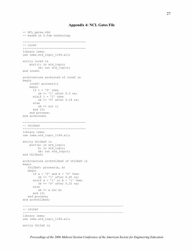
3.6 Asynchronous Logic Assignments and NCL VHDL Library To test the students’ understanding of asynchronous logic design, they were given one homework assignment over the concepts presented above (see Appendix 1), and one VHDL-based group project (see Appendix 2). In order to assist the students with designing and testing NCL circuits in VHDL, an NCL VHDL library was created. The library consists of a package that defines the fundamental NCL data types, as shown in Appendix 3, a file containing the fundamental NCL gates, based on a 0.5µm AMI process, as shown in Appendix 4, a file
Component Output Gate Delays
Type Carry / PPH Sum / PPLQ33mul 1 2 Q332add 3 3 Q322add 2 3 Q32add 2 2 Q2Dadd N/A 1 Q3Dadd N/A 1

Proceedings of the 2006 Midwest Section Conference of the American Society for Engineering Education
18
containing generic versions of standard NCL registration and completion components, as shown in Appendix 5, and a package consisting of various functions to be used in testbenches, as shown in Appendix 6. 4. Course Outline In this project, asynchronous logic design was incorporated into UMR’s Digital System Modeling (CpE 318) course, which focuses on digital circuit design using VHDL. The original course schedule is shown in Figure 20. This provides the students with approximately 13 weeks of topic lectures, leaving around 3 weeks for discussion of homework and project assignments and their solutions, the midterm exam (i.e. the final exam is given the week after the 16-week semester concludes), and holidays. This schedule has been vetted by the author over the past five years and has been shown to work well. It does require the students to do a sizable amount of work; however, after successful completion of the course, students are well versed in VHDL. 1) Introduction to Modeling with VHDL ½ week 2) Entity and Architecture Statements ½ week 3) Test Benches ½ week 4) Basic UNIX commands and Mentor Graphics VHDL compiler and simulator 1/3 week HW#1: design simple behavioral, dataflow, and structural models and testbench 5) Packages, function, and procedures 1 week HW#2: write a package including functions and procedures 6) Mealy and Moore machines 2 weeks HW#3: Mealy and Moore machines, including design, VHDL behavioral and
dataflow implementation, state minimization, and state assignment 7) Algorithmic State Machines (ASMs) 2 weeks 8) Mentor Graphics VHDL synthesis tool 1/3 week HW#4: ASM throughput capability (TPC) calculation, TPC optimization, and VHDL
dataflow implementation and synthesis Design Project #1: design complex chip, such as Run-Length Encoder, Huffman Decoder, etc. Midterm Exam 9) Generic Constants and Generate Statements 1 week HW#5: design a generic Multiply and Accumulate unit (MAC) 10) File I/O 1 week 11) Floating-Point Arithmetic 1 week HW#6: design an IEEE single precision floating-point co-processor 12) Simple RISC Microcontroller Architecture 2 weeks Design Project #2: augment RISC architecture discussed in class to include additional
instructions, such as various branches, a NOP, and a compare, and implement in VHDL, including Text I/O in testbench
13) Overview of Verilog Modeling Language ½ week Final Exam
Figure 20. Original VHDL course schedule. To integrate the asynchronous logic material into the course, the last quarter of the original schedule was revised, as shown in Figure 21. The floating-point arithmetic and microprocessor architecture topics were replaced with the asynchronous topics; HW#5 on generic constants and

Proceedings of the 2006 Midwest Section Conference of the American Society for Engineering Education
19
generate statements was changed to instead cover Text I/O; HW#6 on the design of an IEEE single precision floating-point co-processor was switched with an assignment on NCL; and Design Project #2 on implementing a microcontroller in VHDL and Text I/O was replaced with the design of a complex generic NCL arithmetic circuit. These changes replace 3 weeks of topics with 2 2/3 weeks of asynchronous logic topics, providing an extra 1/3 week for additional explanation of the NCL assignments and solutions. Furthermore, the changes do not eliminate any key VHDL course modules; both floating-point arithmetic and RISC microcontroller architecture are covered in various other Computer Engineering courses, and were only discussed in the VHDL course so that they could be used as sample circuits to be designed in VHDL. Furthermore, since asynchronous circuits must be designed as structural models and cannot be described as behavioral or dataflow models and synthesized using the industry standard tools, the topic fits seamlessly into the discussion of generate statements, which are mostly used in structural models. 1) Introduction to Modeling with VHDL ½ week 2) Entity and Architecture Statements ½ week 3) Test Benches ½ week 4) Basic UNIX commands and Mentor Graphics VHDL compiler and simulator 1/3 week HW#1: design simple behavioral, dataflow, and structural models and testbench 5) Packages, function, and procedures 1 week HW#2: write a package including functions and procedures 6) Mealy and Moore machines 2 weeks HW#3: Mealy and Moore machines, including design and VHDL behavioral and
dataflow implementation, state minimization, and state assignment 7) Algorithmic State Machines (ASMs) 2 weeks 8) Mentor Graphics VHDL synthesis tool 1/3 week HW#4: ASM throughput capability (TPC) calculation, TPC optimization, and VHDL
dataflow implementation and synthesis Design Project #1: design complex chip, such as Run-Length Encoder, Huffman Decoder, etc. Midterm Exam 9) Generic Constants and Generate Statements 1 week 10) File I/O 1 week HW#5: augment the Design Project #1 testbench to read the inputs from a text file
and store the outputs to a text file 11) Overview of Asynchronous Logic 1/3 week 12) Overview of NCL ½ week 13) Input-Completeness and Observability ½ week 14) NCL Dual-Rail Combinational Logic Design ½ week 15) NCL Pipelining Optimization ½ week HW#6: NCL assignment (see Appendix 1) 16) Asynchronous Circuit Synthesis 1/3 week Design Project #2: design NCL generic arithmetic circuit, such as a MAC, iterative
divider, greatest common divisor (GCD), etc. (see Appendix 2) 17) Overview of Verilog Modeling Language ½ week Final Exam
Figure 21. Revised VHDL course schedule.

Proceedings of the 2006 Midwest Section Conference of the American Society for Engineering Education
20
5. Conclusions and Future Work Overall, the students found the asynchronous logic topics very interesting, and performed quite well on the related assignments. The class average on the asynchronous logic homework assignment was the second highest of the six homeworks (i.e. 83% verses 86%, 76%, 73%, 64%, and 44%). The asynchronous project’s average was approximately the same as the first project (i.e. 85% verses 87%); however, this includes one group of two students whom decided not to complete the project, and therefore received a 31% on the partial submission. Excluding this outlier boosts the asynchronous project’s average to 91%. The knowledge gained in this course will better prepare students for the challenges faced by the digital design community for years to come. This work will be continued next semester, as asynchronous logic topics are also incorporated into UMR’s Introduction to VLSI course, so that students will have a better chance of being exposed to asynchronous logic design. The VLSI course will cover some of the same fundamental topics discussed in the VHDL course, but will focus on lower level design issues, such as transistor-level NCL gate design, how the internal feedback (i.e. hysteresis) within NCL gates affects a circuit’s testability, and various NCL gate implementations (i.e. static, semi-static, and dynamic 13).The VLSI course will culminate with the design of a large NCL circuit, using the Mentor Graphics design tools. NCL transistor-level, physical-level, and Design-For-Test (DFT) libraries are currently being developed for the Mentor Graphics toolset for use in this course, using a 0.18µm TSMC process. Furthermore, the VHDL library is also being updated. Specifically, the NCL gates file will be updated with revised propagation delays based on the new 0.18µm TSMC physical-level library being developed; and functions for converting between std_logic, dual_rail_logic, and quad_rail_logic will be added to the NCL functions package. These libraries are available for download at: www.ece.umr.edu/~smithsco/CCLI_async. *** comment: website currently under development *** Bibliography 1) I. E. Sutherland, “Micropipelines,” Communications of the ACM, Vol. 32/6, pp. 720-738, 1989. 2) A.J. Martin, “Programming in VLSI: From Communicating Processes to Delay-Insensitive Circuits,” in
Developments in Concurrency and Communication, UT Year of Programming Institute on Concurrent Programming, Addison-Wesley, 1990, pp. 1-64.
3) K. Van Berkel, “Beware the Isochronic Fork,” Integration, the VLSI Journal, Vol. 13/2, pp. 103-128, 1992. 4) Y. Kim and F. Lombardi, “Guest Editors’ Introduction: Clockless VLSI Systems,” IEEE Design and Test of
Computers: Special Issue on Clockless VLSI Design, Vol. 30/6, pp. 26-36, November-December 2003. 5) D. E. Muller, “Asynchronous Logics and Application to Information Processing,” in Switching Theory in Space
Technology, Stanford University Press, pp. 289-297, 1963. 6) C. L. Seitz, “System Timing,” in Introduction to VLSI Systems, Addison-Wesley, pp. 218-262, 1980. 7) J. Sparso, J. Staunstrup, M. Dantzer-Sorensen, “Design of Delay Insensitive Circuits using Multi-Ring
Structures,” Proceedings of the European Design Automation Conference, pp. 15-20, 1992. 8) T. S. Anantharaman, “A Delay Insensitive Regular Expression Recognizer,” IEEE VLSI Technical Bulletin,
Sept. 1986.
Proceedings of the 2006 Midwest Section Conference of the American Society for Engineering Education
21
9) N. P. Singh, A Design Methodology for Self-Timed Systems, Master’s Thesis, MIT/LCS/TR-258, Laboratory for Computer Science, MIT, 1981.
10) I. David, R. Ginosar, and M. Yoeli, “An Efficient Implementation of Boolean Functions as Self-Timed Circuits,” IEEE Transactions on Computers, Vol. 41/1, pp. 2-10, 1992.
11) D. H. Linder and J. H. Harden, “Phased logic: supporting the synchronous design paradigm with delay-insensitive circuitry,” IEEE Transactions on Computers, Vol. 45/9, pp. 1031-1044, 1996.
12) K. M. Fant and S. A. Brandt, “NULL Convention Logic: A Complete and Consistent Logic for Asynchronous Digital Circuit Synthesis,” International Conference on Application Specific Systems, Architectures, and Processors, pp. 261-273, 1996.
13) Gerald E. Sobelman and Karl M. Fant, “CMOS Circuit Design of Threshold Gates with Hysteresis,” IEEE International Symposium on Circuits and Systems (II), pp. 61-65, 1998.
14) S. C. Smith, R. F. DeMara, J. S. Yuan, D. Ferguson, and D. Lamb, “Optimization of NULL Convention Self-Timed Circuits,” Integration, the VLSI Journal, Vol. 37/3, pp. 135-165, August 2004.
15) A. J. Martin, “Compiling Communicating Processes into Delay-Insensitive VLSI Circuits,” Distributed Computing, Vol. 1/4, pp. 226-234, 1986.
16) S. C. Smith, R. F. DeMara, J. S. Yuan, M. Hagedorn, and D. Ferguson, “Delay-Insensitive Gate-Level Pipelining,” Integration, the VLSI Journal, Vol. 30/2, pp. 103-131, October 2001.
17) M. L. Dertouzos, Threshold Logic: A Synthesis Approach, Cambridge, M. I. T. Press, 1965. 18) Lewis & Coates, Threshold Logic, New York: John Wiley & Sons, Inc., 1967. 19) C. Sheng, Threshold Logic, New York: Ryerson Press, 1969. 20) S. C. Smith, “Completion-Completeness for NULL Convention Digital Circuits Utilizing the Bit-wise
Completion Strategy,” The 2003 International Conference on VLSI, pp. 143-149, June 2003. 21) J. Ebergen, “Arbiters: An Exercise in Specifying and Decomposing Asynchronously Communicating
Components,” Science of Computer Programming, 18(3), pp. 223-245, 1992. 22) K. van Berkel, “Handshake Circuits: an Asynchronous Architecture for VLSI Programming,” International
Series on Parallel Computation, Vol. 5, Cambridge University Press, 1993. 23) A.M.G. Peeters, Single-Rail Handshake Circuits, Ph.D. Thesis, Eindhoven University of Technology, 1996. 24) A. Bardsley and D. Edwards, “Compiling the Language Balsa to Delay-Insensitive Hardware,” Hardware
Description Languages and their Applications (CHDL), April 1997, pp. 89-91. 25) T. Chelcea, A. Bardsley, D. Edwards, and S. M. Nowick, “A Burst-Mode Oriented Back-End for the Balsa
Synthesis System,” Design, Automation and Test in Europe Conference and Exhibition, pp. 330-337, March 2002.
26) R. B. Reese, M. A. Thornton, and C. Traver, “A coarse-grain phased logic CPU,” IEEE Transactions on Computers, Vol. 54, No. 7, pp. 788-799, 2005.
27) A. Kondratyev, L. Neukom, O. Roig, A. Taubin, and K. Fant, “Checking Delay-Insensitivity: 104 Gates and Beyond,” Eighth International Symposium on Asynchronous Circuits and Systems, pp. 149-157, April 2002.
SCOTT C. SMITH is an assistant professor of Computer Engineering at UMR. He received BSEE and BSCpE degrees from the University of Missouri – Columbia (UMC) in 1996. He then received an MSEE degree from UMC in 1998, and a PhD in CpE from the University of Central Florida in 2001. Dr. Smith is very interested in integrating industrial design tools and real-world design problems into his courses. He is a member of ASEE, Sigma Xi, Eta Kappa Nu, Tau Beta Pi, and a senior member of IEEE.

Proceedings of the 2006 Midwest Section Conference of the American Society for Engineering Education
22
Appendix 1: Homework Assignment on Asynchronous Logic Design
CpE 318 HW#6 (due Tuesday, May 2) (5 points each for a total of 20 points)
1) Design a fully observable and input-complete dual-rail 2:1 multiplexer having a worse-case
delay of no more than two gates. The inputs are D0, D1, and S, which are all dual-rail signals. The output is F, which is also a dual-rail signal.
2) In order to maximize throughput for a dual-rail pipelined unsigned Booth2 multiplier, the
partial product generation is partitioned into two parts. The first part recodes each group of three dual-rail multiplier signals (MR2 MR1 MR0) into a dual-rail signal, S, and a quad-rail select signal, sel. S = 0 if the partial product is positive; and S = 1 if the partial product is negative. sel = 0 if the partial product is +0; sel = 1 if the partial product is ±MD; sel = 2 if the partial product is ±2MD; and sel = 3 if the partial product is -0. These two signals, S and sel, are then used as inputs to the second part, along with the dual-rail multiplicand signals, MDi and MDi-1, to generate the corresponding partial product bit, PPi.
a) Below is the circuitry to generate PPi.
3
S1
3
S0 sel3 sel2 sel1 sel0
2 PP i0
MDi1 MDi
0 MDi-11 MDi-1
0
AND0AB
DC
3
3
2 PP i1
AND0AB
DC
i) Is this circuit input-complete with respect to any of its inputs? Explain. ii) Is this circuit observable? Explain. If not, make it observable, but do not change its input-
completeness or increase its worse-case delay.

Proceedings of the 2006 Midwest Section Conference of the American Society for Engineering Education
23
3) For the following quad-rail multiplier: i) Put an “X” through each component in the critical path(s). What is TDD for this non-pipelined
design? ii) If you were to maximize the throughput using full-word completion, what is the optimal TDD
and what is the minimal number of stages required? Show your work. iii) If you were to maximize the throughput using bit-wise completion, what is the optimal TDD
and what is the minimal number of stages required? Show your work.
Q33mulQ33mulQ33mulQ33mul
PPLPPHPPLPPHPPLPPHPPLPPH
MD1 MD0MR1 MR0
BA BA BB A A
P0P1P2P3
Q32add
Sq
Xq Yq
Cd
Q33add
Sq
Xq Yq
Cd
Q32add
Sq
Xq Yq
Cd
Q32add
Sq
Xq Yq
Cd
Q3DDadd
Cd Sq
Xq Yd Zd
Q2DDadd
Sq
Xq Yd Zd
Q3Dadd
Sq
Xq Yd
Component Output Gate Delays Type Carry / PPH Sum / PPL
Q33mul 1 2 Q33add 2 2 Q32add 2 2 Q3DDadd 2 2 Q2DDadd N/A 2 Q3Dadd N/A 1

Proceedings of the 2006 Midwest Section Conference of the American Society for Engineering Education
4) Redraw the following circuit using both full-word and bit-wise completion. Which completion strategy is better in terms of area? Which is better in terms of speed? Explain.

Proceedings of the 2006 Midwest Section Conference of the American Society for Engineering Education
25
Appendix 2: Group Project on Asynchronous Logic Design
CpE 318, Section A: Design Project #2 (due Tuesday, May 9)
* This project can be done in groups of up to three. Groups must be approved by me no later
than Tuesday, April 18. No collaboration between groups is permitted. Identical or nearly identical solutions will result in both groups receiving NO CREDIT (at my discretion).
Problem: Design a Generic NCL 2s Complement MAC * entity name: MAC * generic constants: X_len, Y_len: positive, default to 4 (X_len ≤ Y_len);
A_len: positive, default to 8 * inputs: X, Y: arbitrary length dual_rail_logic_vector (assume ≥ 4); reset, Ki: std_logic * outputs: A: arbitrary length dual_rail_logic_vector (assume ≥ X_len+Y_len);
OV: dual_rail_logic; Ko: std_logic * name your file: MAC_group#.vhd * include as comments: name and student number of group members * use the array structured multiplication algorithm * email your main design, components, and testbench(es) as attachments from the PC
(ftp to PC) to: [email protected] * your design will then be run on my testbenches * make sure that all names and input/output order match those on this sheet, otherwise your
design will not run on my testbenches and points will be deducted * Turn in a report including the following - project description - Block Diagram of MAC Chip - gate-level design of MAC components (i.e. FA, HA, AND2, NAND2, FA1, HA1,
OVcomp, etc.) - component level diagram of the following sized MACs > 8+4×4 > 12+5×4
- MAC VHDL code - VHDL testbench(es), testing 8+4×4 and 12+5×4 MACs
- simulation macro(s) Hints: - register the overflow and take both OV and A from the register output - remember that at least 3 registers are required in a feedback loop to avoid deadlock - the following example constructs may be helpful: type twoD_array is array(3 downto 0, 3 downto 0) of dual_rail_logic; signal intermediate: twoD_array; intermediate(3, 0) <= D; -- D is defined as dual_rail_logic

Proceedings of the 2006 Midwest Section Conference of the American Society for Engineering Education
26
Appendix 3: NCL Data Types Package
-- NCL_signals.vhd Library IEEE; use IEEE.std_logic_1164.all; package ncl_signals is type quad_rail_logic is record RAIL3 : std_logic; RAIL2 : std_logic; RAIL1 : std_logic; RAIL0 : std_logic; end record; type quad_rail_logic_vector is array (NATURAL range <>) of quad_rail_logic; type dual_rail_logic is record RAIL1 : std_logic; RAIL0 : std_logic; end record; type dual_rail_logic_vector is array (NATURAL range <>) of dual_rail_logic; end ncl_signals;
Proceedings of the 2006 Midwest Section Conference of the American Society for Engineering Education
27
Appendix 4: NCL Gates File
-- NCL_gates.vhd -- based on 0.5um technology ------------------------------------- -- invx0 ------------------------------------- library ieee; use ieee.std_logic_1164.all; entity invx0 is port(i: in std_logic; zb: out std_logic); end invx0; architecture archinvx0 of invx0 is begin invx0: process(i) begin if i = '0' then zb <= '1' after 0.3 ns; elsif i = '1' then zb <= '0' after 0.18 ns; else zb <= not i; end if; end process; end archinvx0; ------------------------------------- -- th12bx0 ------------------------------------- library ieee; use ieee.std_logic_1164.all; entity th12bx0 is port(a: in std_logic; b: in std_logic; zb: out std_logic); end th12bx0; architecture archth12bx0 of th12bx0 is begin th12bx0: process(a, b) begin if a = '0' and b = '0' then zb <= '1' after 0.45 ns; elsif a = '1' or b = '1' then zb <= '0' after 0.22 ns; else zb <= a nor b; end if; end process; end archth12bx0; ----------------------------------------------------------- -- th12x0 ----------------------------------------------------------- library ieee; use ieee.std_logic_1164.all; entity th12x0 is

Proceedings of the 2006 Midwest Section Conference of the American Society for Engineering Education
28
port(a: in std_logic; b: in std_logic; z: out std_logic); end th12x0; architecture archth12x0 of th12x0 is begin th12x0: process(a, b) begin if a = '0' and b = '0' then z <= '0' after 0.65 ns; elsif a = '1' or b = '1' then z <= '1' after 0.45 ns; else z <= a or b; end if; end process; end archth12x0; ------------------------------------- -- th13bx0 ------------------------------------- library ieee; use ieee.std_logic_1164.all; entity th13bx0 is port(a: in std_logic; b: in std_logic; c: in std_logic; zb: out std_logic); end th13bx0; architecture archth13bx0 of th13bx0 is begin th13bx0: process(a,b,c) begin if a = '0' and b = '0' and c= '0' then zb <= '1' after 0.65 ns; elsif a = '1' or b = '1' or c= '1' then zb <= '0' after 0.32 ns; else zb <= not(a or b or c); end if; end process; end archth13bx0; ----------------------------------------------------------- -- th13x0 ----------------------------------------------------------- library ieee; use ieee.std_logic_1164.all; entity th13x0 is port(a: in std_logic; b: in std_logic; c: in std_logic; z: out std_logic); end th13x0; architecture archth13x0 of th13x0 is begin th13x0: process(a, b, c) begin

Proceedings of the 2006 Midwest Section Conference of the American Society for Engineering Education
29
if a = '0' and b = '0' and c = '0' then z <= '0' after 0.75 ns; elsif a = '1' or b = '1' or c = '1' then z <= '1' after 0.55 ns; else z <= a or b or c; end if; end process; end archth13x0; ----------------------------------------------------------- -- th14bx0 ----------------------------------------------------------- library ieee; use ieee.std_logic_1164.all; entity th14bx0 is port(a: in std_logic; b: in std_logic; c: in std_logic; d: in std_logic; zb: out std_logic); end th14bx0; architecture archth14bx0 of th14bx0 is begin th14bx0: process(a, b, c, d) begin if a = '0' and b = '0' and c = '0' and d = '0' then zb <= '1' after 0.32 ns; elsif a = '1' or b = '1' or c = '1' or d = '1' then zb <= '0' after 0.65 ns; else zb <= not(a or b or c or d); end if; end process; end archth14bx0; ----------------------------------------------------------- -- th14x0 ----------------------------------------------------------- library ieee; use ieee.std_logic_1164.all; entity th14x0 is port(a: in std_logic; b: in std_logic; c: in std_logic; d: in std_logic; z: out std_logic); end th14x0; architecture archth14x0 of th14x0 is begin th14x0: process(a, b, c, d) begin if a = '0' and b = '0' and c = '0' and d = '0' then z <= '0' after 0.75 ns; elsif a = '1' or b = '1' or c = '1' or d = '1' then z <= '1' after 0.55 ns; else z <= a or b or c or d; end if;

Proceedings of the 2006 Midwest Section Conference of the American Society for Engineering Education
30
end process; end archth14x0; ----------------------------------------------------------- -- th22dx0 ----------------------------------------------------------- library ieee; use ieee.std_logic_1164.all; entity th22dx0 is port(a: in std_logic; b: in std_logic; rst: in std_logic; z: out std_logic ); end th22dx0; architecture archth22dx0 of th22dx0 is begin th22dx0: process(a, b, rst) begin if rst = '1' then -- reset z <= '1' after 0.23 ns; elsif (a= '1' and b= '1') then z <= '1' after 0.23 ns; elsif (a= '0' and b= '0') then z <= '0' after 0.19 ns; end if; end process; end archth22dx0; ----------------------------------------------------------- -- th22nx0 ----------------------------------------------------------- library ieee; use ieee.std_logic_1164.all; entity th22nx0 is port(a: in std_logic; b: in std_logic; rst: in std_logic; z: out std_logic ); end th22nx0; architecture archth22nx0 of th22nx0 is begin th22nx0: process(a, b, rst) begin if rst = '1' then -- reset z <= '0' after 0.16 ns; elsif (a= '1' and b= '1') then z <= '1' after 0.29 ns; elsif (a= '0' and b= '0') then z <= '0' after 0.16 ns; end if; end process; end archth22nx0; ----------------------------------------------------------- -- th22x0 ----------------------------------------------------------- library ieee; use ieee.std_logic_1164.all;

Proceedings of the 2006 Midwest Section Conference of the American Society for Engineering Education
31
entity th22x0 is port(a: in std_logic; b: in std_logic; z: out std_logic ); end th22x0; architecture archth22x0 of th22x0 is begin th22x0: process(a, b) begin if (a= '1' and b= '1') then z <= '1' after 0.4 ns; elsif (a= '0' and b= '0') then z <= '0' after 0.2 ns; end if; end process; end archth22x0; ----------------------------------------------------------- -- th23w2x0 ----------------------------------------------------------- library ieee; use ieee.std_logic_1164.all; entity th23w2x0 is port(a: in std_logic; -- weight 2 b: in std_logic; c: in std_logic; z: out std_logic ); end th23w2x0; architecture archth23w2x0 of th23w2x0 is begin th23w2x0: process(a, b, c) begin if (a= '0' and b= '0' and c= '0') then z <= '0' after 0.28 ns; elsif (a= '1' or (b= '1' and c= '1')) then z <= '1' after 0.47 ns; end if; -- else NULL end process; end archth23w2x0; ----------------------------------------------------------- -- th23x0 ----------------------------------------------------------- library ieee; use ieee.std_logic_1164.all; entity th23x0 is port(a: in std_logic; b: in std_logic; c: in std_logic; z: out std_logic ); end th23x0; architecture archth23x0 of th23x0 is begin th23x0: process(a, b, c) begin if (a= '0' and b= '0' and c= '0') then z <= '0' after 0.28 ns;

Proceedings of the 2006 Midwest Section Conference of the American Society for Engineering Education
32
elsif (a= '1' and b= '1') or (b= '1' and c= '1') or (c= '1' and a= '1') then z <= '1' after 0.47 ns; end if; end process; end archth23x0; ----------------------------------------------------------- -- th24x0 ----------------------------------------------------------- library ieee; use ieee.std_logic_1164.all; entity th24x0 is port(a: in std_logic; b: in std_logic; c: in std_logic; d: in std_logic; z: out std_logic ); end th24x0; architecture archth24x0 of th24x0 is begin th24x0: process(a, b, c, d) begin if (a= '0' and b= '0' and c= '0' and d = '0') then z <= '0' after 0.28 ns; elsif ((a= '1' and b= '1') or (a= '1' and c= '1') or (a= '1' and d= '1') or (b= '1' and c= '1') or (b= '1' and d= '1') or (c= '1' and d = '1')) then z <= '1' after 0.4 ns; end if; -- else NULL end process; end archth24x0; ----------------------------------------------------------- -- th24w22x0 ----------------------------------------------------------- library ieee; use ieee.std_logic_1164.all; entity th24w22x0 is port(a: in std_logic; -- weight 2 b: in std_logic; -- weight 2 c: in std_logic; d: in std_logic; z: out std_logic ); end th24w22x0; architecture archth24w22x0 of th24w22x0 is begin th24w22x0: process(a, b, c, d) begin if (a= '0' and b= '0' and c= '0' and d = '0') then z <= '0' after 0.28 ns; elsif (a= '1' or b= '1' or (c= '1' and d = '1')) then z <= '1' after 0.47 ns; end if; -- else NULL end process; end archth24w22x0;

Proceedings of the 2006 Midwest Section Conference of the American Society for Engineering Education
33
----------------------------------------------------------- -- th24w2x0 ----------------------------------------------------------- library ieee; use ieee.std_logic_1164.all; entity th24w2x0 is port(a: in std_logic; -- weight 2 b: in std_logic; c: in std_logic; d: in std_logic; z: out std_logic ); end th24w2x0; architecture archth24w2x0 of th24w2x0 is begin th24w2x0: process(a, b, c, d) begin if (a= '0' and b= '0' and c= '0' and d = '0') then z <= '0' after 0.28 ns; elsif (a= '1' or (b= '1' and c= '1') or (b= '1' and d = '1') or (c= '1' and d= '1')) then z <= '1' after 0.47 ns; end if; -- else NULL end process; end archth24w2x0; ----------------------------------------------------------- -- th33dx0 ----------------------------------------------------------- library ieee; use ieee.std_logic_1164.all; entity th33dx0 is port(a: in std_logic; b: in std_logic; c: in std_logic; rst: in std_logic; z: out std_logic ); end th33dx0; architecture archth33dx0 of th33dx0 is begin th33dx0: process(a, b, c, rst) begin if rst = '1' then z <= '1' after 0.23 ns; elsif (a= '1' and b= '1' and c= '1') then z <= '1' after 0.57 ns; elsif (a= '0' and b= '0' and c= '0') then z <= '0' after 0.25 ns; end if; -- else NULL end process; end archth33dx0; ----------------------------------------------------------- -- th33nx0 ----------------------------------------------------------- library ieee; use ieee.std_logic_1164.all; entity th33nx0 is port(a: in std_logic;

Proceedings of the 2006 Midwest Section Conference of the American Society for Engineering Education
34
b: in std_logic; c: in std_logic; rst: in std_logic; z: out std_logic ); end th33nx0; architecture archth33nx0 of th33nx0 is begin th33nx0: process(a, b, c, rst) begin if rst = '1' then z <= '0' after 0.16 ns; elsif (a= '1' and b= '1' and c= '1') then z <= '1' after 0.57 ns; elsif (a= '0' and b= '0' and c= '0') then z <= '0' after 0.25 ns; end if; -- else NULL end process; end archth33nx0; ----------------------------------------------------------- -- th33x0 ----------------------------------------------------------- library ieee; use ieee.std_logic_1164.all; entity th33x0 is port(a: in std_logic; b: in std_logic; c: in std_logic; z: out std_logic ); end th33x0; architecture archth33x0 of th33x0 is begin th33x0: process(a, b, c) begin if (a= '1' and b= '1' and c= '1') then z <= '1' after 0.57 ns; elsif (a= '0' and b= '0' and c= '0') then z <= '0' after 0.28 ns; end if; -- else NULL end process; end archth33x0; ----------------------------------------------------------- -- th33w2x0 ----------------------------------------------------------- library ieee; use ieee.std_logic_1164.all; entity th33w2x0 is port(a: in std_logic; -- weight 2 b: in std_logic; c: in std_logic; z: out std_logic ); end th33w2x0; architecture archth33w2x0 of th33w2x0 is begin th33w2x0: process(a, b, c) begin if (a= '0' and b= '0' and c= '0') then

Proceedings of the 2006 Midwest Section Conference of the American Society for Engineering Education
35
z <= '0' after 0.28 ns; elsif (a= '1' and (b= '1' or c= '1')) then z <= '1' after 0.47 ns; end if; -- else NULL end process; end archth33w2x0; ----------------------------------------------------------- --th34w22x0 ----------------------------------------------------------- library ieee; use ieee.std_logic_1164.all; entity th34w22x0 is port(a: in std_logic; -- weight 2 b: in std_logic; -- weight 2 c: in std_logic; d: in std_logic; z: out std_logic ); end th34w22x0; architecture archth34w22x0 of th34w22x0 is begin th34w22x0: process(a, b, c, d) begin if (a= '0' and b= '0' and c= '0' and d = '0') then z <= '0' after 0.28 ns; elsif (a = '1' and b = '1') or (a = '1' and c = '1') or (a = '1' and d = '1') or (b = '1' and c = '1') or (b = '1' and d = '1') then z <= '1' after 0.47 ns; end if; -- else NULL end process; end archth34w22x0; ----------------------------------------------------------- --th34w2x0 ----------------------------------------------------------- library ieee; use ieee.std_logic_1164.all; entity th34w2x0 is port(a: in std_logic; -- weight 2 b: in std_logic; c: in std_logic; d: in std_logic; z: out std_logic ); end th34w2x0; architecture archth34w2x0 of th34w2x0 is begin th34w2x0: process(a, b, c, d) begin if (a= '0' and b= '0' and c= '0' and d = '0') then z <= '0' after 0.28 ns; elsif (a = '1' and b = '1') or (a = '1' and c = '1') or (a = '1' and d = '1') or (b = '1' and c = '1' and d = '1') then z <= '1' after 0.47 ns; end if; -- else NULL end process; end archth34w2x0;

Proceedings of the 2006 Midwest Section Conference of the American Society for Engineering Education
36
----------------------------------------------------------- -- th34w32x0 ----------------------------------------------------------- library ieee; use ieee.std_logic_1164.all; entity th34w32x0 is port(a: in std_logic; -- weight 3 b: in std_logic; -- weight 2 c: in std_logic; d: in std_logic; z: out std_logic ); end th34w32x0; architecture archth34w32x0 of th34w32x0 is begin th34w32x0: process(a, b, c, d) begin if (a= '0' and b= '0' and c= '0' and d = '0') then z <= '0' after 0.28 ns; elsif (a= '1' or (b= '1' and (c= '1' or d = '1') ) ) then z <= '1' after 0.47 ns; end if; -- else NULL end process; end archth34w32x0; ----------------------------------------------------------- -- th34w3x0 ----------------------------------------------------------- library ieee; use ieee.std_logic_1164.all; entity th34w3x0 is port(a: in std_logic; -- weight 3 b: in std_logic; c: in std_logic; d: in std_logic; z: out std_logic ); end th34w3x0; architecture archth34w3x0 of th34w3x0 is begin th34w3x0: process(a, b, c, d) begin if (a= '0' and b= '0' and c= '0' and d = '0') then z <= '0' after 0.28 ns; elsif (a= '1' or (b= '1' and c= '1' and d = '1')) then z <= '1' after 0.47 ns; end if; -- else NULL end process; end archth34w3x0; ----------------------------------------------------------- -- th34x0 ----------------------------------------------------------- library ieee; use ieee.std_logic_1164.all; entity th34x0 is port(a: in std_logic; b: in std_logic; c: in std_logic; d: in std_logic;

Proceedings of the 2006 Midwest Section Conference of the American Society for Engineering Education
37
z: out std_logic ); end th34x0; architecture archth34x0 of th34x0 is begin th34w3x0: process(a, b, c, d) begin if (a= '0' and b= '0' and c= '0' and d = '0') then z <= '0' after 0.28 ns; elsif ((a= '1' and b= '1' and c= '1') or (a= '1' and c= '1' and d= '1') or (a= '1' and b= '1' and d= '1') or (b= '1' and c= '1' and d= '1')) then z <= '1' after 0.47 ns; end if; -- else NULL end process; end archth34x0; ----------------------------------------------------------- -- th44x0 ----------------------------------------------------------- library ieee; use ieee.std_logic_1164.all; entity th44x0 is port(a: in std_logic; b: in std_logic; c: in std_logic; d: in std_logic; z: out std_logic ); end th44x0; architecture archth44x0 of th44x0 is begin th44x0: process(a, b, c, d) begin if (a= '1' and b= '1' and c= '1' and d= '1') then z <= '1' after 0.57 ns; elsif (a= '0' and b= '0' and c= '0' and d= '0') then z <= '0' after 0.25 ns; end if; -- else NULL end process; end archth44x0; ----------------------------------------------------------- -- th44w22x0 ----------------------------------------------------------- library ieee; use ieee.std_logic_1164.all; entity th44w22x0 is port(a: in std_logic; -- weight 2 b: in std_logic; -- weight 2 c: in std_logic; d: in std_logic; z: out std_logic ); end th44w22x0; architecture archth44w22x0 of th44w22x0 is begin th44w22x0: process(a, b, c, d) begin if ((a= '1' and b= '1') or

Proceedings of the 2006 Midwest Section Conference of the American Society for Engineering Education
38
(a= '1' and c= '1' and d= '1') or (b= '1' and c= '1' and d= '1')) then z <= '1' after 0.57 ns; elsif (a= '0' and b= '0' and c= '0' and d= '0') then z <= '0' after 0.25 ns; end if; -- else NULL end process; end archth44w22x0; ----------------------------------------------------------- -- th44w2x0 ----------------------------------------------------------- library ieee; use ieee.std_logic_1164.all; entity th44w2x0 is port(a: in std_logic; -- weight 2 b: in std_logic; c: in std_logic; d: in std_logic; z: out std_logic ); end th44w2x0; architecture archth44w2x0 of th44w2x0 is begin th44w2x0: process(a, b, c, d) begin if ((a= '1' and b= '1' and c= '1') or (a= '1' and b= '1' and d= '1') or (a= '1' and c= '1' and d= '1')) then z <= '1' after 0.57 ns; elsif (a= '0' and b= '0'and c= '0' and d= '0') then z <= '0' after 0.25 ns; end if; -- else NULL end process; end archth44w2x0; ----------------------------------------------------------- -- th44w322x0 ----------------------------------------------------------- library ieee; use ieee.std_logic_1164.all; entity th44w322x0 is port(a: in std_logic; -- weight 3 b: in std_logic; -- weight 2 c: in std_logic; -- weight 2 d: in std_logic; z: out std_logic ); end th44w322x0 ; architecture archth44w322x0 of th44w322x0 is begin th44w322x0: process(a, b, c, d) begin if (a= '0' and b= '0' and c= '0' and d = '0') then z <= '0' after 0.28 ns; elsif ( a = '1' and ( b = '1' or c = '1' or d = '1')) or ( b = '1' and c = '1' ) then z <= '1' after 0.47 ns; end if; -- else NULL end process; end archth44w322x0;

Proceedings of the 2006 Midwest Section Conference of the American Society for Engineering Education
39
----------------------------------------------------------- -- th44w3x0 ----------------------------------------------------------- library ieee; use ieee.std_logic_1164.all; entity th44w3x0 is port(a: in std_logic; -- weight 3 b: in std_logic; c: in std_logic; d: in std_logic; z: out std_logic ); end th44w3x0; architecture archth44w3x0 of th44w3x0 is begin th44w3x0: process(a, b, c, d) begin if (a= '0' and b= '0' and c= '0' and d = '0') then z <= '0' after 0.28 ns; elsif a = '1' and ( b = '1' or c = '1' or d = '1' ) then z <= '1' after 0.47 ns; end if; -- else NULL end process; end archth44w3x0 ; ----------------------------------------------------------- -- th54w22x0 ----------------------------------------------------------- library ieee; use ieee.std_logic_1164.all; entity th54w22x0 is port(a: in std_logic; -- weight 2 b: in std_logic; -- weight 2 c: in std_logic; d: in std_logic; z: out std_logic ); end th54w22x0; architecture archth54w22x0 of th54w22x0 is begin th54w22x0: process(a, b, c, d) begin if (a= '0' and b= '0' and c= '0' and d = '0') then z <= '0' after 0.28 ns; elsif (a= '1' and b= '1' and (c= '1' or d = '1')) then z <= '1' after 0.47 ns; end if; -- else NULL end process; end archth54w22x0; ----------------------------------------------------------- -- th54w322x0 ----------------------------------------------------------- library ieee; use ieee.std_logic_1164.all; entity th54w322x0 is port(a: in std_logic; -- weight 3 b: in std_logic; -- weight 2 c: in std_logic; -- weight 2 d: in std_logic;

Proceedings of the 2006 Midwest Section Conference of the American Society for Engineering Education
40
z: out std_logic ); end th54w322x0; architecture archth54w322x0 of th54w322x0 is begin th54w322x0: process(a, b, c, d) begin if (a= '0' and b= '0'and c= '0' and d = '0') then z <= '0' after 0.28 ns; elsif (a= '1' and b= '1') or (a = '1' and c= '1') or (b= '1' and c='1' and d= '1') then z <= '1' after 0.47 ns; end if; -- else NULL end process; end archth54w322x0; ----------------------------------------------------------- -- th54w32x0 ----------------------------------------------------------- library ieee; use ieee.std_logic_1164.all; entity th54w32x0 is port(a: in std_logic; -- weight 3 b: in std_logic; -- weight 2 c: in std_logic; d: in std_logic; z: out std_logic ); end th54w32x0; architecture archth54w32x0 of th54w32x0 is begin th54w32x0: process(a, b, c, d) begin if (a= '0' and b= '0' and c= '0' and d = '0') then z <= '0' after 0.28 ns; elsif (a= '1' and b= '1') or (a = '1' and c= '1' and d = '1') then z <= '1' after 0.47 ns; end if; -- else NULL end process; end archth54w32x0; ----------------------------------------------------------- -- thand0x0 ----------------------------------------------------------- library ieee; use ieee.std_logic_1164.all; entity thand0x0 is port(a: in std_logic; b: in std_logic; c: in std_logic; d: in std_logic; z: out std_logic ); end thand0x0; architecture archthand0x0 of thand0x0 is begin thand0x0: process(a, b, c, d) begin if (a= '0' and b= '0' and c= '0' and d = '0') then z <= '0' after 0.28 ns;

Proceedings of the 2006 Midwest Section Conference of the American Society for Engineering Education
41
elsif ((a = '1' and b = '1') or (b = '1' and c = '1') or (a = '1' and d = '1')) then z <= '1' after 0.47 ns; end if; -- else NULL end process; end archthand0x0; ----------------------------------------------------------- -- th24compx0 ----------------------------------------------------------- library ieee; use ieee.std_logic_1164.all; entity th24compx0 is port(a: in std_logic; b: in std_logic; c: in std_logic; d: in std_logic; z: out std_logic ); end th24compx0; architecture archth24compx0 of th24compx0 is begin th24compx0: process(a, b, c, d) begin if (a= '0' and b= '0' and c= '0' and d = '0') then z <= '0' after 0.28 ns; elsif (a = '1' or b = '1') and (c = '1' or d = '1') then z <= '1' after 0.47 ns; end if; -- else NULL end process; end archth24compx0; ----------------------------------------------------------- -- thxor0x0 ----------------------------------------------------------- library ieee; use ieee.std_logic_1164.all; entity thxor0x0 is port(a: in std_logic; b: in std_logic; c: in std_logic; d: in std_logic; z: out std_logic ); end thxor0x0; architecture archthxor0x0 of thxor0x0 is begin thxor0x0: process(a, b, c, d) begin if (a= '0' and b= '0' and c= '0' and d = '0') then z <= '0' after 0.28 ns; elsif (a = '1' and b = '1') or (c = '1' and d = '1') then z <= '1' after 0.47 ns; end if; -- else NULL end process; end archthxor0x0;

Proceedings of the 2006 Midwest Section Conference of the American Society for Engineering Education
42
Appendix 5: NCL Components File
-- NCL_components.vhd -- Package used for Completion Component Library IEEE; use IEEE.std_logic_1164.all; package tree_funcs is function log_u(L: integer; R: integer) return integer; -- ceiling of Log base R of L function level_number(width, level, base: integer) return integer; -- bits to be combined on level of tree of width using base input gates end tree_funcs; package body tree_funcs is function log_u(L: integer; R: integer) return integer is variable temp: integer := 1; variable level: integer := 0; begin if L = 1 then return 0; end if; while temp < L loop temp := temp * R; level := level + 1; end loop; return level; end; function level_number(width, level, base: integer) return integer is variable num: integer := width; begin if level /= 0 then for i in 1 to level loop if (log_u((num / base) + (num rem base), base) + i) = log_u(width, base) then num := (num / base) + (num rem base); else num := (num / base) + 1; end if; end loop; end if; return num; end; end tree_funcs; -- Generic Completion Component library ieee; use ieee.std_logic_1164.all; use work.tree_funcs.all; entity comp is generic(width: in integer := 4); port(a: IN std_logic_vector(width-1 downto 0); ko: OUT std_logic);

Proceedings of the 2006 Midwest Section Conference of the American Society for Engineering Education
43
end comp; architecture arch of comp is type completion is array(log_u(width, 4) downto 0, width-1 downto 0) of std_logic; signal comp_array: completion; component th22x0 port(a: in std_logic; b: in std_logic; z: out std_logic); end component; component th33x0 port(a: in std_logic; b: in std_logic; c: in std_logic; z: out std_logic); end component; component th44x0 port(a: in std_logic; b: in std_logic; c: in std_logic; d: in std_logic; z: out std_logic); end component; begin RENAME: for i in 0 to width-1 generate comp_array(0, i) <= a(i); end generate; STRUCTURE: for k in 0 to log_u(width, 4)-1 generate begin NOT_LAST: if level_number(width, k, 4) > 4 generate begin PRINCIPLE: for j in 0 to (level_number(width, k, 4) / 4)-1 generate G4: th44x0 port map(comp_array(k, j*4), comp_array(k, j*4+1), comp_array(k, j*4+2), comp_array(k, j*4+3), comp_array(k+1, j)); end generate; LEFT_OVER_GATE: if log_u((level_number(width, k, 4) / 4) + (level_number(width, k, 4) rem 4), 4) + k + 1 /= log_u(width, 4) generate begin NEED22: if (level_number(width, k, 4) rem 4) = 2 generate G2: th22x0 port map(comp_array(k, level_number(width, k, 4)-2), comp_array(k, level_number(width, k, 4)-1), comp_array(k+1, (level_number(width, k, 4) / 4))); end generate; NEED33: if (level_number(width, k, 4) rem 4) = 3 generate G3: th33x0 port map(comp_array(k, level_number(width, k, 4)-3), comp_array(k, level_number(width, k, 4)-2), comp_array(k, level_number(width, k, 4)-1), comp_array(k+1, (level_number(width, k, 4) / 4)));

Proceedings of the 2006 Midwest Section Conference of the American Society for Engineering Education
44
end generate; end generate; LEFT_OVER_SIGNALS: if (log_u((level_number(width, k, 4) / 4) + (level_number(width, k, 4) rem 4), 4) + k + 1 = log_u(width, 4)) and ((level_number(width, k, 4) rem 4) /= 0) generate begin RENAME_SIGNALS: for h in 0 to (level_number(width, k, 4) rem 4)-1 generate comp_array(k+1, (level_number(width, k, 4) / 4)+h) <= comp_array(k, level_number(width, k, 4)-1-h); end generate; end generate; end generate; LAST22: if level_number(width, k, 4) = 2 generate G2F: th22x0 port map(comp_array(k, 0), comp_array(k, 1), ko); end generate; LAST33: if level_number(width, k, 4) = 3 generate G3F: th33x0 port map(comp_array(k, 0), comp_array(k, 1), comp_array(k, 2), ko); end generate; LAST44: if level_number(width, k, 4) = 4 generate G4F: th44x0 port map(comp_array(k, 0), comp_array(k, 1), comp_array(k, 2), comp_array(k, 3), ko); end generate; end generate; end arch; -- 1-bit Dual-Rail Register use work.ncl_signals.all; library ieee; use ieee.std_logic_1164.all; entity ncl_register_D1 is generic(initial_value: integer := -1); -- 1=DATA1, 0=DATA0, -1=NULL port(D: in dual_rail_logic; ki: in std_logic; rst: in std_logic; Q: out dual_rail_logic; ko: out std_logic); end ncl_register_D1; architecture arch of ncl_register_d1 is signal Qbuf: dual_rail_logic; component th22nx0 port (a, b, rst: IN std_logic; z: OUT std_logic); end component; component th22dx0 port (a, b, rst: IN std_logic; z: OUT std_logic);

Proceedings of the 2006 Midwest Section Conference of the American Society for Engineering Education
45
end component; component th12bx0 port (a, b: IN std_logic; zb: OUT std_logic); end component; begin RstN: if initial_value = -1 generate R0: th22nx0 port map(D.rail0, ki, rst, Qbuf.rail0); R1: th22nx0 port map(D.rail1, ki, rst, Qbuf.rail1); end generate; Rst1: if initial_value = 1 generate R0: th22nx0 port map(D.rail0, ki, rst, Qbuf.rail0); R1: th22dx0 port map(D.rail1, ki, rst, Qbuf.rail1); end generate; Rst0: if initial_value = 0 generate R0: th22dx0 port map(D.rail0, ki, rst, Qbuf.rail0); R1: th22nx0 port map(D.rail1, ki, rst, Qbuf.rail1); end generate; Q <= Qbuf; COMP: th12bx0 port map(Qbuf.rail0, Qbuf.rail1, ko); end; -- Generic Length Dual-Rail Register use work.ncl_signals.all; library ieee; use ieee.std_logic_1164.all; entity ncl_register_D is generic(width: positive := 2 ; initial_value: integer := -1); -- 1=DATA1, 0=DATA0, -1=NULL port(D: in dual_rail_logic_vector(width-1 downto 0); ki: in std_logic_vector(width-1 downto 0); rst: in std_logic; Q: out dual_rail_logic_vector(width-1 downto 0); ko: out std_logic_vector(width-1 downto 0)); end ncl_register_D; architecture gen of ncl_register_D is component ncl_register_D1 generic(initial_value: integer := -1); -- 1=DATA1, 0=DATA0, -1=NULL port(D: in dual_rail_logic; ki: in std_logic; rst: in std_logic; Q: out dual_rail_logic; ko: out std_logic);

Proceedings of the 2006 Midwest Section Conference of the American Society for Engineering Education
46
end component; begin gen_reg: for i in 0 to D'length-1 generate REGi: ncl_register_D1 generic map(initial_value) port map(D(i), ki(i), rst, Q(i), ko(i)); end generate; end; -- 1-bit Quad-Rail Register use work.ncl_signals.all; library ieee; use ieee.std_logic_1164.all; entity ncl_register_Q1 is generic(initial_value: integer := -1); -- 3=DATA3, 2=DATA2, 1=DATA1, 0=DATA0, -1=NULL port(D: in quad_rail_logic; ki: in std_logic; rst: in std_logic; Q: out quad_rail_logic; ko: out std_logic); end ncl_register_Q1; architecture arch of ncl_register_Q1 is signal Qbuf: quad_rail_logic; component th22nx0 port (a, b, rst: IN std_logic; z: OUT std_logic); end component; component th22dx0 port (a, b, rst: IN std_logic; z: OUT std_logic); end component; component th14bx0 port (a, b, c, d: IN std_logic; zb: OUT std_logic); end component; begin RstN: if initial_value = -1 generate R0: th22nx0 port map(D.rail0, ki, rst, Qbuf.rail0); R1: th22nx0 port map(D.rail1, ki, rst, Qbuf.rail1); R2: th22nx0 port map(D.rail2, ki, rst, Qbuf.rail2); R3: th22nx0 port map(D.rail3, ki, rst, Qbuf.rail3); end generate; Rst3: if initial_value = 3 generate R0: th22nx0 port map(D.rail0, ki, rst, Qbuf.rail0);

Proceedings of the 2006 Midwest Section Conference of the American Society for Engineering Education
47
R1: th22nx0 port map(D.rail1, ki, rst, Qbuf.rail1); R2: th22nx0 port map(D.rail2, ki, rst, Qbuf.rail2); R3: th22dx0 port map(D.rail3, ki, rst, Qbuf.rail3); end generate; Rst2: if initial_value = 2 generate R0: th22nx0 port map(D.rail0, ki, rst, Qbuf.rail0); R1: th22nx0 port map(D.rail1, ki, rst, Qbuf.rail1); R2: th22dx0 port map(D.rail2, ki, rst, Qbuf.rail2); R3: th22nx0 port map(D.rail3, ki, rst, Qbuf.rail3); end generate; Rst1: if initial_value = 1 generate R0: th22nx0 port map(D.rail0, ki, rst, Qbuf.rail0); R1: th22dx0 port map(D.rail1, ki, rst, Qbuf.rail1); R2: th22nx0 port map(D.rail2, ki, rst, Qbuf.rail2); R3: th22nx0 port map(D.rail3, ki, rst, Qbuf.rail3); end generate; Rst0: if initial_value = 0 generate R0: th22dx0 port map(D.rail0, ki, rst, Qbuf.rail0); R1: th22nx0 port map(D.rail1, ki, rst, Qbuf.rail1); R2: th22nx0 port map(D.rail2, ki, rst, Qbuf.rail2); R3: th22nx0 port map(D.rail3, ki, rst, Qbuf.rail3); end generate; Q <= Qbuf; COMP: th14bx0 port map(Qbuf.rail0, Qbuf.rail1, Qbuf.rail2, Qbuf.rail3, ko); end;

Proceedings of the 2006 Midwest Section Conference of the American Society for Engineering Education
48
-- Generic Length Quad-Rail Register use work.ncl_signals.all; library ieee; use ieee.std_logic_1164.all; entity ncl_register_Q is generic(width: positive := 2 ; initial_value: integer := -1); -- 3=DATA3, 2=DATA2, 1=DATA1, 0=DATA0, -1=NULL port(D: in quad_rail_logic_vector(width-1 downto 0); ki: in std_logic_vector(width-1 downto 0); rst: in std_logic; Q: out quad_rail_logic_vector(width-1 downto 0); ko: out std_logic_vector(width-1 downto 0)); end ncl_register_Q; architecture gen of ncl_register_Q is component ncl_register_Q1 generic(initial_value: integer := -1); -- 3=DATA3, 2=DATA2, 1=DATA1, 0=DATA0, -1=NULL port(D: in quad_rail_logic; ki: in std_logic; rst: in std_logic; Q: out quad_rail_logic; ko: out std_logic); end component; begin gen_reg: for i in 0 to D'length-1 generate REGi: ncl_register_Q1 generic map(initial_value) port map(D(i), ki(i), rst, Q(i), ko(i)); end generate; end;

Proceedings of the 2006 Midwest Section Conference of the American Society for Engineering Education
49
Appendix 6: NCL Functions Package
-- NCL_functions.vhd -- to be used in testbenches -- not to be synthesized Library IEEE; use IEEE.std_logic_1164.all; use work.ncl_signals.all; package functions is function is_null(s: DUAL_RAIL_LOGIC_VECTOR) return BOOLEAN; function is_data(s: DUAL_RAIL_LOGIC_VECTOR) return BOOLEAN; function is_null(s: DUAL_RAIL_LOGIC) return BOOLEAN; function is_data(s: DUAL_RAIL_LOGIC) return BOOLEAN; function is_null(s: QUAD_RAIL_LOGIC_VECTOR) return BOOLEAN; function is_data(s: QUAD_RAIL_LOGIC_VECTOR) return BOOLEAN; function is_null(s: QUAD_RAIL_LOGIC) return BOOLEAN; function is_data(s: QUAD_RAIL_LOGIC) return BOOLEAN; end functions; package body functions is function is_null(s: DUAL_RAIL_LOGIC_VECTOR) return BOOLEAN is begin for i in 0 to s'length - 1 loop if s(i).rail0 = '0' and s(i).rail1 = '0' then null; else return FALSE; end if; end loop; return TRUE; end is_null; function is_data(s: DUAL_RAIL_LOGIC_VECTOR) return BOOLEAN is begin for i in 0 to s'length - 1 loop if s(i).rail0 = '1' or s(i).rail1 = '1' then null; else return FALSE; end if; end loop; return TRUE; end is_data; function is_null(s: DUAL_RAIL_LOGIC) return BOOLEAN is begin if s.rail0 = '0' and s.rail1 = '0' then return TRUE; else return FALSE; end if; end is_null; function is_data(s: DUAL_RAIL_LOGIC) return BOOLEAN is begin if s.rail0 = '1' or s.rail1 = '1' then return TRUE; else

Proceedings of the 2006 Midwest Section Conference of the American Society for Engineering Education
50
return FALSE; end if; end is_data; function is_null(s: QUAD_RAIL_LOGIC_VECTOR) return BOOLEAN is begin for i in 0 to s'length - 1 loop if s(i).rail0 = '0' and s(i).rail1 = '0' and s(i).rail2 = '0' and s(i).rail3 = '0' then null; else return FALSE; end if; end loop; return TRUE; end is_null; function is_data(s: QUAD_RAIL_LOGIC_VECTOR) return BOOLEAN is begin for i in 0 to s'length - 1 loop if s(i).rail0 = '1' or s(i).rail1 = '1' or s(i).rail2 = '1' or s(i).rail3 = '1' then null; else return FALSE; end if; end loop; return TRUE; end is_data; function is_null(s: QUAD_RAIL_LOGIC) return BOOLEAN is begin if s.rail0 = '0' and s.rail1 = '0' and s.rail2 = '0' and s.rail3 = '0' then return TRUE; else return FALSE; end if; end is_null; function is_data(s: QUAD_RAIL_LOGIC) return BOOLEAN is begin if s.rail0 = '1' or s.rail1 = '1' or s.rail2 = '1' or s.rail3 = '1' then return TRUE; else return FALSE; end if; end is_data; end functions;