integrated parylene-cabled silicon probes for neural prosthetics · 2012-06-22 · recent advances...
TRANSCRIPT

INTEGRATED PARYLENE-CABLED SILICON PROBES FOR NEURAL PROSTHETICS
R. Huang1, C. Pang1, Y.C. Tai1, J. Emken2, C. Ustun2, R. Andersen2 and J. Burdick3
1Caltech Micromachining Group, California Institute of Technology, Pasadena, CA 2Division of Biology, California Institute of Technology, Pasadena, CA
3Department of Mechanical Engineering, California Institute of Technology, Pasadena, CA
ABSTRACT Recent advances in the field of neural prosthetics have demonstrated the thought control of a computer cursor. This capability relies primarily on electrode array surgically implanted into the brain as an acquisition source of neural activity. Various technologies have been developed for signal extraction; however most suffer from either fragile electrode shanks and bulky cables or inefficient use of surgical site areas. Here we present a design and initial testing results from high electrode density, silicon based arrays system with an integrated parylene cable. The greatly reduced flexible rigidity of the parylene cable is believed to relief possible mechanical damages due to relative motion between a brain and its skull. 1. INTRODUCTION Regardless of the particular technology used to accomplish neural prosthesis, an ideal wired multi-electrode array would consist of: (1) biocompatible materials, (2) high density electrodes with high signal-to-noise ratio (3) reliable, high density cables and a percutaneous interconnect to communicate with peripherals and (4) ability to accommodate integrated circuitries for on-probe signal amplification. Current state technologies have yet to balance the trade-offs between these criteria. A few have well controlled metal electrode fabrication and circuitry integration techniques but have designs that are brittle and difficult to handle. On the other hand, some have reliable interconnect cables but are weak on IC expansion capability [1 - 3] In this work, we present a parylene coated silicon probe that has the potential to overcome these difficulties. A major improvement of the current device over its predecessor [4] is the complete encapsulation of the array with parylene. We recall that the previous generation consisted of a silicon substrate that was exposed on all sides except the front side, significantly reducing the biocompatibility of the device. As before, we have chosen to use parylene C (poly-para-xylylene C) due to its insulative capability, flexibility, biocompatibility, and its prior use in medical applications. Furthermore, our flexible parylene-based cable has a cross section that is 500 µm wide and 15 µm thick and is designed to route the signals acquired with a 32 channel array. It is a major feature of our device that the cabling is not a component that is later attached to the array but that it is simply an integrated extension of the top parylene structure of the array itself. The resulting manufacturing simplification is expected to significantly improve the reliability of our device. Finally, this monolithically micromachined cable – probe system is able to accommodate future chip integrations through the addition
or modification of the silicon pieces on the silicon probe. As a result, we are able to fabricate silicon probe devices that are highly customizable, fully biocompatible, and easy to mass fabricate which will facilitate future research in developing a neural prosthetic system. 2. DESIGN A flexible parylene lift-off technology [5] allows us to fabricate 2-D 32 channel flexible cabled electrode array devices (Figure 1). These devices can be expanded to 3-D 32N channel structures by probe stacking of N number of 2D probes. Platinum electrodes on each of the eight silicon shanks can be spaced at configurable intervals and two reference electrodes are located on two of the longer shanks. The shank lengths range from 3 mm to 12 mm and are 150 µm thick and 60 µm wide towards the tip of the shank. The tip of the shank forms a 10° angle to facilitate the insertion into the brain.
Figure 1. SEM picture of the electrodes on the silicon shanks Figure 2 - 4 show the unpackaged cabled silicon probes and their bonding interface. The circular platinum rings arranged in a 60° Y shape pattern on the end of device are used to electrically bond to commercial available connectors with conductive epoxy on a circular PC board. The parylene cables (7 cm long) are 15 µm thick and have 34 traces lines of 10 µm wide and spaced 10 µm apart connect the distal electrodes directly to external connectors [6] (Figure 5).
Figure 2. Released silicon probe with parylene flexible cable.
978-1-4244-1793-3/08/$25.00 ©2008 IEEE MEMS 2008, Tucson, AZ, USA, January 13-17, 2008240
Authorized licensed use limited to: CALIFORNIA INSTITUTE OF TECHNOLOGY. Downloaded on April 16,2010 at 23:16:10 UTC from IEEE Xplore. Restrictions apply.
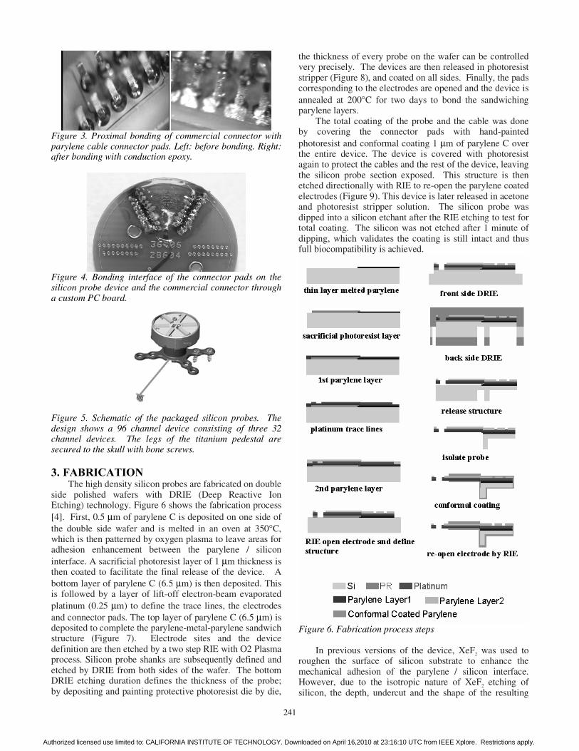
Figure 3. Proximal bonding of commercial connector with parylene cable connector pads. Left: before bonding. Right: after bonding with conduction epoxy.
Figure 4. Bonding interface of the connector pads on the silicon probe device and the commercial connector through a custom PC board.
Figure 5. Schematic of the packaged silicon probes. The design shows a 96 channel device consisting of three 32 channel devices. The legs of the titanium pedestal are secured to the skull with bone screws. 3. FABRICATION The high density silicon probes are fabricated on double side polished wafers with DRIE (Deep Reactive Ion Etching) technology. Figure 6 shows the fabrication process [4]. First, 0.5 µm of parylene C is deposited on one side of the double side wafer and is melted in an oven at 350°C, which is then patterned by oxygen plasma to leave areas for adhesion enhancement between the parylene / silicon interface. A sacrificial photoresist layer of 1 µm thickness is then coated to facilitate the final release of the device. A bottom layer of parylene C (6.5 µm) is then deposited. This is followed by a layer of lift-off electron-beam evaporated platinum (0.25 µm) to define the trace lines, the electrodes and connector pads. The top layer of parylene C (6.5 µm) is deposited to complete the parylene-metal-parylene sandwich structure (Figure 7). Electrode sites and the device definition are then etched by a two step RIE with O2 Plasma process. Silicon probe shanks are subsequently defined and etched by DRIE from both sides of the wafer. The bottom DRIE etching duration defines the thickness of the probe; by depositing and painting protective photoresist die by die,
the thickness of every probe on the wafer can be controlled very precisely. The devices are then released in photoresist stripper (Figure 8), and coated on all sides. Finally, the pads corresponding to the electrodes are opened and the device is annealed at 200°C for two days to bond the sandwiching parylene layers. The total coating of the probe and the cable was done by covering the connector pads with hand-painted photoresist and conformal coating 1 µm of parylene C over the entire device. The device is covered with photoresist again to protect the cables and the rest of the device, leaving the silicon probe section exposed. This structure is then etched directionally with RIE to re-open the parylene coated electrodes (Figure 9). This device is later released in acetone and photoresist stripper solution. The silicon probe was dipped into a silicon etchant after the RIE etching to test for total coating. The silicon was not etched after 1 minute of dipping, which validates the coating is still intact and thus full biocompatibility is achieved.
Figure 6. Fabrication process steps In previous versions of the device, XeF2 was used to roughen the surface of silicon substrate to enhance the mechanical adhesion of the parylene / silicon interface. However, due to the isotropic nature of XeF2 etching of silicon, the depth, undercut and the shape of the resulting
241
Authorized licensed use limited to: CALIFORNIA INSTITUTE OF TECHNOLOGY. Downloaded on April 16,2010 at 23:16:10 UTC from IEEE Xplore. Restrictions apply.

surface becomes hard to control. This may result in broken metal lines as well as thermal stress cracks on the border lines during the high temperature electron beam evaporation of platinum. Thus, the melted parylene alternative was used to enhance the adhesion of the desired area.
Figure 7. Process wafer after top layer parylene deposition
Figure 8. a) Tapered 5 mm length silicon array after releasing from the wafer. b) Platinum electrode pads under microscope
Figure 9. a) SEM picture of electrode. b) Sidewall etching after the final opening of the electrodes after total coating. 4. EXPERIMENTS AND RESULT Device testing was performed in three phases: in-vitro measurements in saline solution, in-vivo probe penetration testing and accelerated life testing. In the first phase, we used the setup shown in Figure 10 to conduct in-vitro impedance tests with channel electrodes having mean dimensions 22 µm x 22 µm. The measured distribution of areas of these electrodes was determined to lie within ±9.1 µm2 of the nominal value under SEM measurements. Impedance measurements of channel electrodes resulted in values of 670 kΩ ±33 kΩ at 1 kHz whereas the reference electrodes with areas approximately 25,000 µm2 resulted in impedances in the range of 20 kΩ. To test the electrode’s ability to pick up signal different signal types, sine waves and pre-recorded action potentials were applied across a saline solution and were successfully recorded with the fabricated electrodes (Figures 11). Impedance tests were also performed on the parylene flexible cable to determine the stray capacitances. Results
show a clear linear relationship on a log-log scale in Figure 12, which allows us to derive the impedance of the cross-talk and the leakage to be approximately 27.4 MΩ and 11.7 MΩ respectively at 1 kΩ.
Figure 10. In vitro testing setup. The metal box on the left hand side is a pre-amplifier. The x-y stage in the Faraday cage maneuvers the probe into the saline solution.
Figure 11. a) Sine wave applied across a saline solution recorded with the silicon probe. b) Threshold aligned waveforms. The horizontal axis is the number of samples taken at the rate of 20,000 samples per second for a duration of 1.2 ms. The vertical axis represents the signal strength corresponding to a sinusoid with amplitude (above baseline) of 400 µV. Secondly, the devices were inserted through the pia and into the cortex of live rats to test penetration ability. Results show a full insertion of the probe was successful without any bending, buckling or breakage by observing the shanks under a surgical microscope during insertion. Finally, the devices underwent accelerated life testing in saline to determine the mean time to failure. Failure modes include the failure of the silicon to parylene adhesion as well as the delamination between the parylene layers. Soaking test results show that the parylene-silicon adhesion is able to withstand more than five weeks in 90°C saline (Figure 13) before delamination occurs. Furthermore, the parylene cable quality is uncompromised for the four weeks of soaking in the same environment with a cable only device (Figure 14).
5mm
300 mm a) b)
a) b)
a) b)
242
Authorized licensed use limited to: CALIFORNIA INSTITUTE OF TECHNOLOGY. Downloaded on April 16,2010 at 23:16:10 UTC from IEEE Xplore. Restrictions apply.

Figure 12. Stray Capacitance with cross talk (relative to neighboring traces) and leakage capacitance (relative to saline). Only the cable was immersed into the solution
Figure 13. Delamination occurrence after five weeks of soaking in 90°C saline solution. Probe was still attached on the parylene cable after eight weeks of soaking.
Figure 14. Parylene cable has same line resistance after four week of soaking in 90°C saline.
5. CONCLUSIONS We have developed and performance tested a fully parylene C encapsulated, high electrode density silicon based array with an integrated flexible cable. A 3-D packaging scheme with commercial connectors and a percutaneous pedestal is also presented. Electrode impedances were characterized and pre-recorded action potentials were recorded through these devices. In vivo insertion capability of the silicon probes have also been verified. High temperature accelerated life time testing in saline indicates the stability of both the cable and the probe-cable interface for more than four weeks in 90°C saline. From the testing results, this high density silicon probe shows promise as a neural probe to be incorporated into a future chronic cortical prosthetic. Future work is underway to optimize the electrode placement and probe shank geometry to accommodate rat anatomy for in-vivo chronic experiments. ACKNOWLEDGEMENTS This work is supported by Defense Advanced Research Projects Agency (DARPA) (Award # 908165) and by National Institute of Health (NIH) moveable probe project (Award # R01EY015545). The authors also would like to thank Mr. Trevor Roper, Agnes Tong, other members of the Caltech Micromachining Laboratory and members of the Andersen lab at Caltech for their advice and help. REFERENCES [1] K. Jones, P. Campbell, R. Normann, “A Glass / Silicon
Composite Intracortical Electrode Array”, Ann Biomed Eng. 1992;20(4):423-37
[2] K.D. Wise, D.J. Anderson, J.F. Hetke, D.R. Kipke, K. Najafi “Wireless Implantable Microsystems: High-Density Electronic Interfaces to the Nervous System”, Proceedings of the IEEE, Vol. 92, No. 1, 2004.
[3] S. Musallam, M.J. Bak, P.R. Troyk, R.A. Andersen, "A floating metal microelectrode array for chronic implantation." Journal of Neuroscience Methods, 160 (2007) 122–127
[4] C. Pang, S. Musallam, Y.C. Tai, J. W. Burdick, and R. A. Andersen, "Novel Monolithic Silicon Probes with Flexible Parylene Cables for Neural Prostheses," IEEE-EMBS MMB, Okinawa, Japan, May 9-12, 2006.
[5] W. Li, D.C. Rodger, J.D. Weiland, M.S. Humayun, Y.C. Tai, “Integrated Flexible Ocular Coil for Power and Data Transfer in Retinal Prostheses”, Proc. 27th Eng. in Med. and Biol. Soc.,2005
[6] D. Rizzuto, S. Musallam, C. Ustun, J. Emken, C. Pang, R. Huang, Y.C. Tai, R. Andersen, The Caltech Neural Prosthetic: Restoring function to paralyzed patients. Society for Neuroscience, 2006
Delamination
Delamination
243
Authorized licensed use limited to: CALIFORNIA INSTITUTE OF TECHNOLOGY. Downloaded on April 16,2010 at 23:16:10 UTC from IEEE Xplore. Restrictions apply.