integrated front-end electronics for sipm detectors in
TRANSCRIPT
Integrated Front-End Electronics for SiPM
Detectors in Medical Imaging Applications
F. Corsi, M. Foresta, F. Licciulli, C. Marzocca, G. Matarrese
DEE - Politecnico di Bari and INFN - Sezione di Bari, Italy
October 26, 2012

Silicon Photo-Multipliers: a short introduction
SiPM model and characterization
Front-end architecture: different approaches
Structure and design of the analog channel
Architecture and design of multichannel ASICs: some examples and results
Alternative architecture
Temperature compensation of SiPM gain
Future work
Outline
October 26, 2012 2
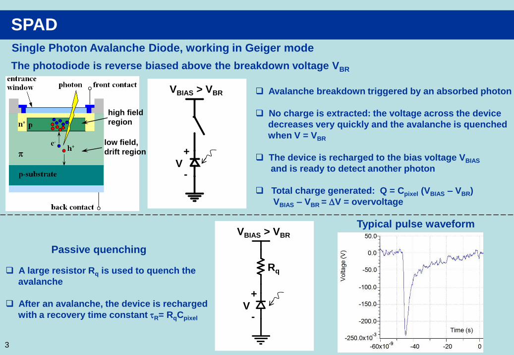
SPAD
Single Photon Avalanche Diode, working in Geiger mode
The photodiode is reverse biased above the breakdown voltage VBR
Avalanche breakdown triggered by an absorbed photon
No charge is extracted: the voltage across the device
decreases very quickly and the avalanche is quenched
when V = VBR
The device is recharged to the bias voltage VBIAS
and is ready to detect another photon
Total charge generated: Q = Cpixel (VBIAS – VBR)
VBIAS – VBR = DV = overvoltage
photon
VBIAS > VBR
V +
-
Passive quenching
VBIAS > VBR
V +
-
Rq A large resistor Rq is used to quench the
avalanche
After an avalanche, the device is recharged
with a recovery time constant tR= RqCpixel
Typical pulse waveform
low field,
drift region
high field
region
3
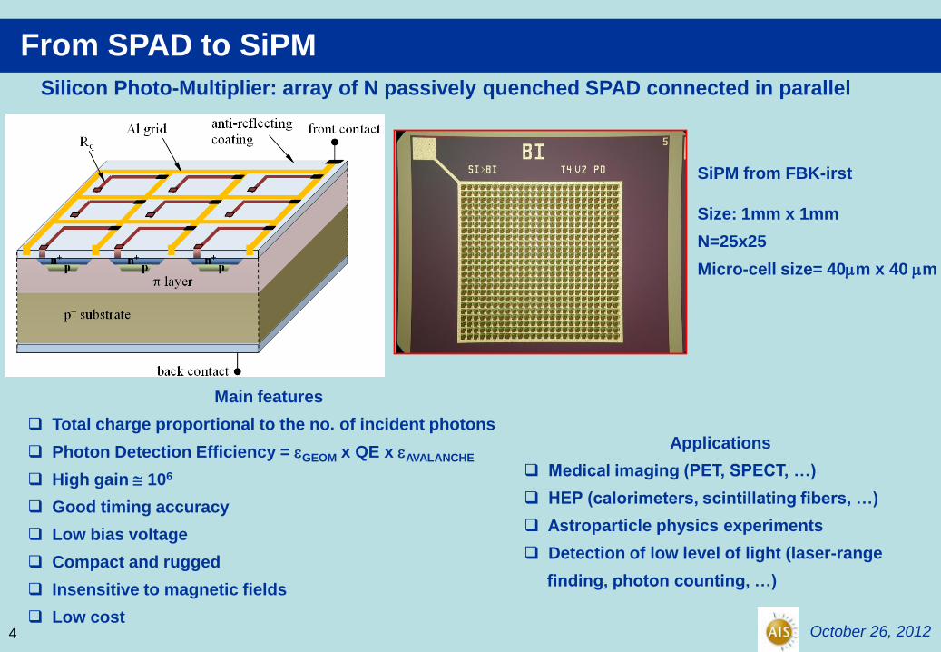
From SPAD to SiPM
Silicon Photo-Multiplier: array of N passively quenched SPAD connected in parallel
SiPM from FBK-irst
Size: 1mm x 1mm
N=25x25
Micro-cell size= 40mm x 40 mm
Main features
Total charge proportional to the no. of incident photons
Photon Detection Efficiency = eGEOM x QE x eAVALANCHE
High gain 106
Good timing accuracy
Low bias voltage
Compact and rugged
Insensitive to magnetic fields
Low cost
Applications
Medical imaging (PET, SPECT, …)
HEP (calorimeters, scintillating fibers, …)
Astroparticle physics experiments
Detection of low level of light (laser-range
finding, photon counting, …)
October 26, 2012 4

SiPM: main limitations
Dark count : an avalanche can be triggered by thermally generated electrons
Optical cross-talk: a photon can be emitted by a micro-cell undergoing avalanche breakdown and can
trigger another avalanche in an adjacent micro-cell
Afterpulsing: the avalanche can be retriggered in a micro-cell during the recovery phase, due to the
release of carriers trapped in deep energy levels
Gain drift with the temperature
Saturation: the probability that one micro-cell is hit by more than one photon becomes significant
October 26, 2012
Afterpulsing Saturation (V. Andreev et al., NIMA 540, pp. 368-380 (2005)
5
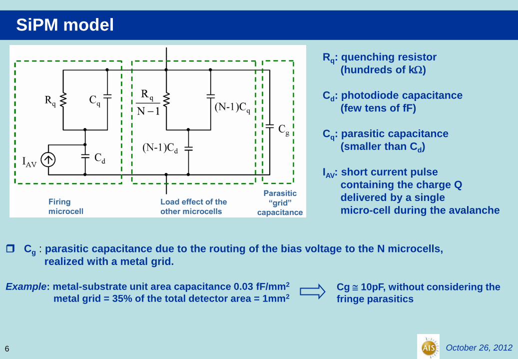
SiPM model
Rq: quenching resistor
(hundreds of kW)
Cd: photodiode capacitance
(few tens of fF)
Cq: parasitic capacitance
(smaller than Cd)
IAV: short current pulse
containing the charge Q
delivered by a single
micro-cell during the avalanche
Cg : parasitic capacitance due to the routing of the bias voltage to the N microcells,
realized with a metal grid.
Example: metal-substrate unit area capacitance 0.03 fF/mm2
metal grid = 35% of the total detector area = 1mm2
Cg 10pF, without considering the
fringe parasitics
October 26, 2012 6
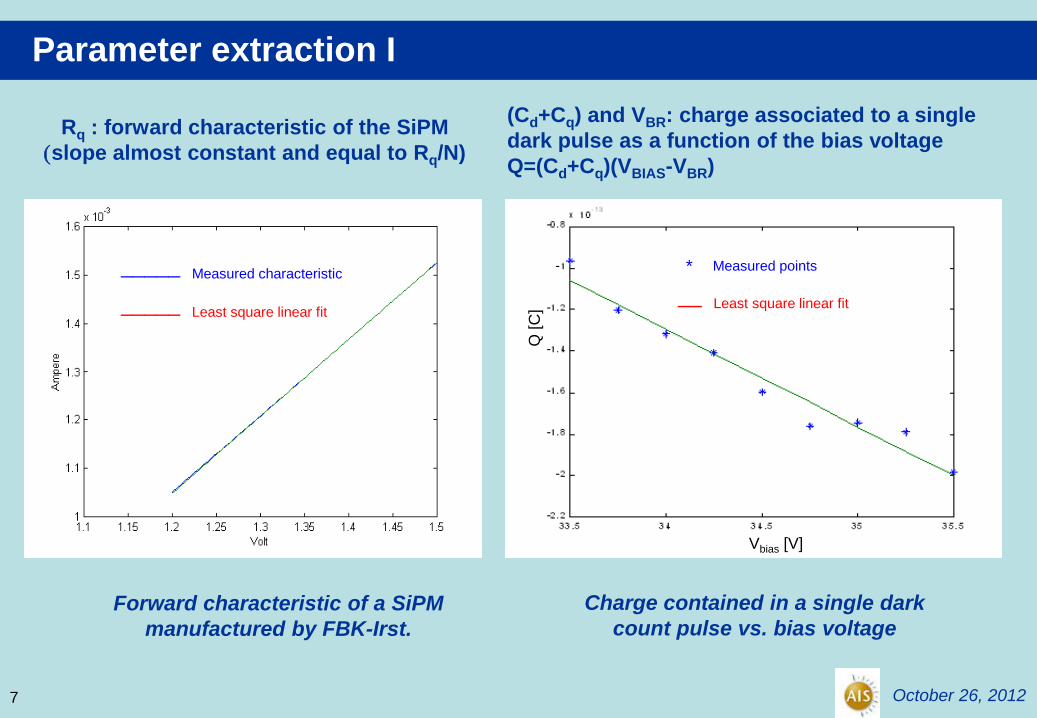
Parameter extraction I
Rq : forward characteristic of the SiPM
(slope almost constant and equal to Rq/N)
_____ Measured characteristic
_____ Least square linear fit
Forward characteristic of a SiPM
manufactured by FBK-Irst.
Vbias [V] Q
[C
]
* Measured points
__ Least square linear fit
Charge contained in a single dark
count pulse vs. bias voltage
(Cd+Cq) and VBR: charge associated to a single
dark pulse as a function of the bias voltage
Q=(Cd+Cq)(VBIAS-VBR)
October 26, 2012 7

Parameter extraction II
CV plotter measurements of the SiPM near the breakdown voltage: YM and CM
According to the SiPM model, YM and CM are expressed in terms of Cdtot=NCd, Cqtot=NCq,
Rqtot=Rq/N and the frequency w of the signal used by the CV plotter.
YM CM
Cqtot
Cg
Cdtot
Rqtot
YM [
mS
]
CM [
pF
]
Vbias [V] Vbias [V]
CV plotter measurement results for a
SiPM manufactured from FBK-Irst.
( qtotdtott2dtotqtot
2
2t
2qtot
2
2dtotqtot
2
M CCC CR CR1
CRY w
w
w
gdtot2t
2qtot
2
dtotqtottgt2qtot
2gdtot
M CCCR1
)CCCC(CRCCC
w
w
Cd,Cq
Cg

Front-end electronics: different approaches I
Charge Sensitive Amplifier
The charge delivered by the detector is collected on Cf
Example:
Maximum DVOUT : 3V
SiPM gain: 106
No of hit microcells: 300
Total charge QTOT : 48pC
Large integration capacitance needed: Cf =16pF
Dynamic range problems
Large silicon area required
Large capacitive loads: power consumption issues or bandwidth limitations
October 26, 2012 9
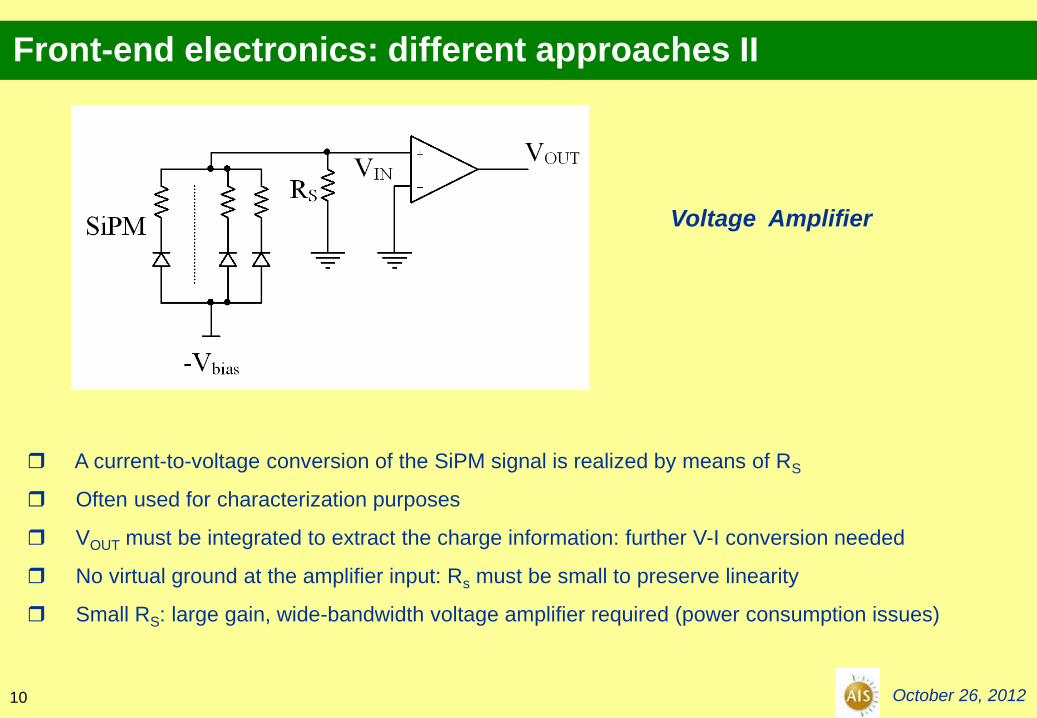
Front-end electronics: different approaches II
A current-to-voltage conversion of the SiPM signal is realized by means of RS
Often used for characterization purposes
VOUT must be integrated to extract the charge information: further V-I conversion needed
No virtual ground at the amplifier input: Rs must be small to preserve linearity
Small RS: large gain, wide-bandwidth voltage amplifier required (power consumption issues)
Voltage Amplifier
October 26, 2012 10

Front-end electronics: different approaches III
Current Amplifier
RS is the very small input impedance of the current amplifier
The output current can be easily replicated (e.g. by means of current mirrors) and further processed
(e.g. integrated)
The circuit is inherently fast (low impedance nodes)
Less problems of dynamic range, also for decreasing supply voltages
October 26, 2012 11

SiPM coupled to the front-end
Cq
A) SiPM coupled to an amplifier with
input impedance Rs
IAV
Rq
Cd (N-1)Cd
(N-1)Cq Rq/(N-1) Cg RS
-
VIN
IIN +
IAV Rq Cd Cq
Iq
Iq
Cg Ceq
-
VIN
+ IIN
RS
B) Simplified circuit (RS << Rq/N)
qdeq C)1N(
1
C)1N(
1
C
1
October 26, 2012
Ceq+Cg = Ctot
12

SiPM + front-end behaviour
Time
0s 20ns 40ns 60ns 80ns 100ns
V(Rin:2) V(C1:2,Vbias)
0V
0.5mV
1.0mV
Time
VIN
Response of the circuits A) and B) to a single dark pulse (160fC) for
three different values of Rs and typical parameter values
Simplified circuit: two time constants
• tIN= Rs (Ceq+Cg) = Rs Ctot
• tr=Rq(Cd+Cq)
The peak of VIN is almost independent of Rs
A fraction QIN of the charge Q delivered
during the avalanche is almost instantly
collected on Ctot
Rs=75W
Rs=50W
Rs=20W
_____ Circuit A)
_____ Circuit B)
qd
q
INCC
CQQ
tot
ININMAX
C
QV
t
t
tt
t
t
tt
tt )
texp()
texp(
QR)t(V
rr
qr
ININ
INq
INr
SIN
( qqq CRt
October 26, 2012 13

Bandwidth of the amplifier
Amplifier output voltage for a single dark pulse: same gain and different bandwidth
Time
0s 10ns 20ns 30ns 40ns 50ns 60ns
V(R2:2)
0V
20.0mV
40.0mV
55.3mV
_____ BW=500MHz
_____ BW=100MHz
Time
VO
UT
Rs=20W
Time
0s 10ns 20ns 30ns 40ns 50ns 60ns
V(R2:2)
0V
50mV
100mV
_____ BW=500MHz
_____ BW=100MHz
Time
VO
UT
Rs=75W
• The bandwidth of the amplifier directly affects the rise time of the waveform
• The peak of the waveform is strongly dependent on the amplifier bandwidth, especially for low values of RS
• The time needed to collect the charge is also slightly influenced by the amplifier bandwidth
• The same conclusions are valid also for the waveform of the output current obtained with a current amplifier
October 26, 2012 14
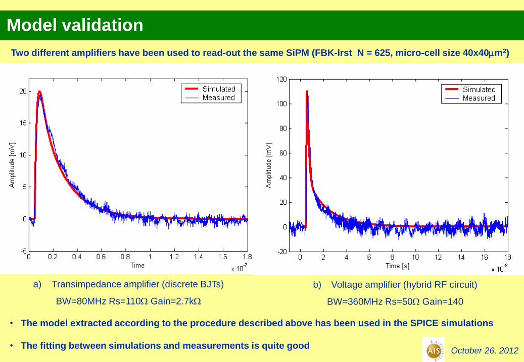
Model validation
Two different amplifiers have been used to read-out the same SiPM (FBK-Irst N = 625, micro-cell size 40x40mm2)
a) Transimpedance amplifier (discrete BJTs)
BW=80MHz Rs=110W Gain=2.7kW
b) Voltage amplifier (hybrid RF circuit)
BW=360MHz Rs=50W Gain=140
• The model extracted according to the procedure described above has been used in the SPICE simulations
• The fitting between simulations and measurements is quite good October 26, 2012
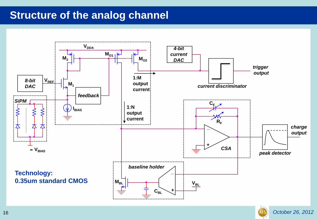
Structure of the analog channel
8-bit
DAC
4-bit
current
DAC
SiPM
VREF
VBIAS
M1
M2
MO1 MO2
feedback
current discriminator
CSA
VDDA
IBIAS 1:N
output
current
1:M
output
current
baseline holder
peak detector
CF
RF
MBL VBL
CBL
+
_
+
_
trigger
output
charge
output
Technology:
0.35um standard CMOS
October 26, 2012 16

Main features and parameters of the analog channel
Current buffer
Small signal bandwidth: 250MHz
(with a 30pF detector)
Low input resistance: 17W
Scaling factors: N=10, M=20
VREF variable in the range 1V÷2V
Total current consumption: 800mA
Fast Current Discriminator
Leading edge
Trise ≈ 300ps
Threshold programmable :
4-bit current DAC from 0 to 40mA
CSA
Continuous passive reset
Variable gain: CF=1pF, 2pF, 3pF
Damping time constant: 200ns
Output voltage range: 0.3V ÷ 2.7V
Baseline holder
Very slow feedback loop
“Ad hoc” techniques to reproduce
large time constants
Small baseline shifts at high event
rates (-1mV @ 100kHz, full dynamic range)
October 26, 2012 17

The current discriminator
Principle of operation
If Iout is less than Ith, then M1 is on and
M2 is off. When Iout becomes greater
than Iref, the MOSFETs switch and the
amplifier output goes low, thus the
inverter output goes high
VDD
VDD
M1
M2
M3
-Av
VDD
Iout
Ith
trigger signal
October 26, 2012 18
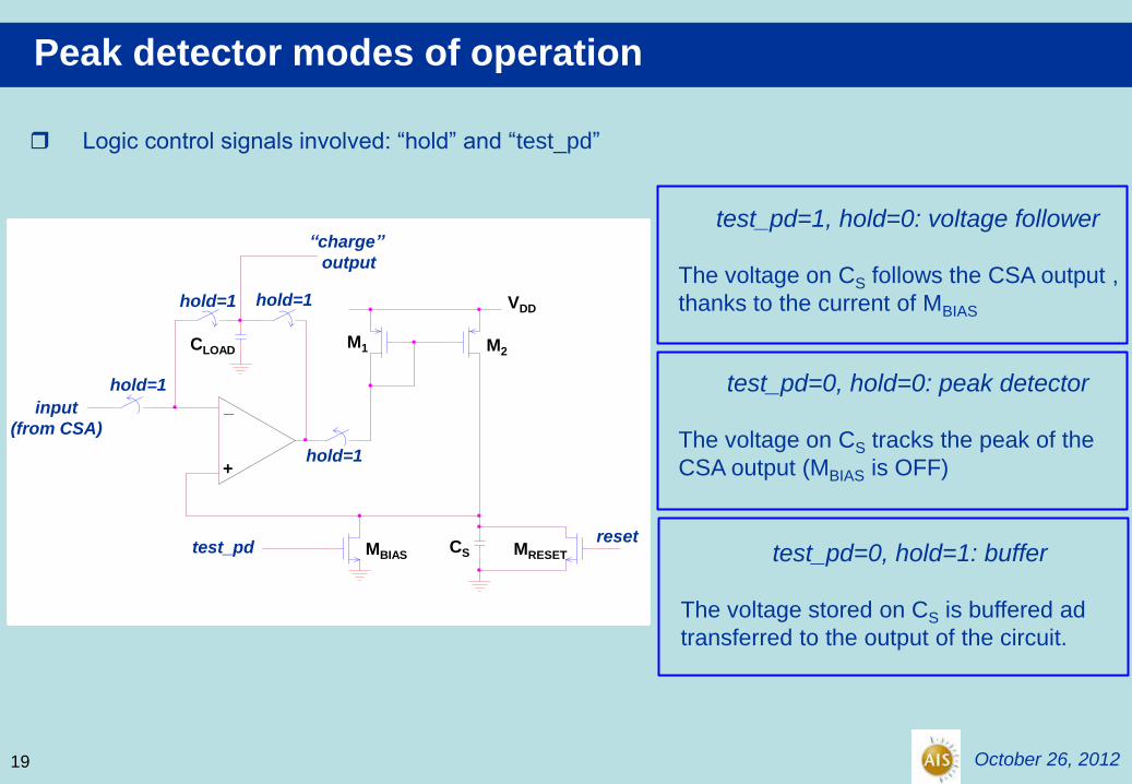
Peak detector modes of operation
Logic control signals involved: “hold” and “test_pd”
+
_
M1
input
(from CSA)
“charge”
output
M2
MBIAS MRESET CS
CLOAD
test_pd reset
hold=1
hold=1
hold=1 hold=1
test_pd=1, hold=0: voltage follower
The voltage on CS follows the CSA output ,
thanks to the current of MBIAS
test_pd=0, hold=0: peak detector
The voltage on CS tracks the peak of the
CSA output (MBIAS is OFF)
test_pd=0, hold=1: buffer
The voltage stored on CS is buffered ad
transferred to the output of the circuit.
October 26, 2012
+
_
VDD
19
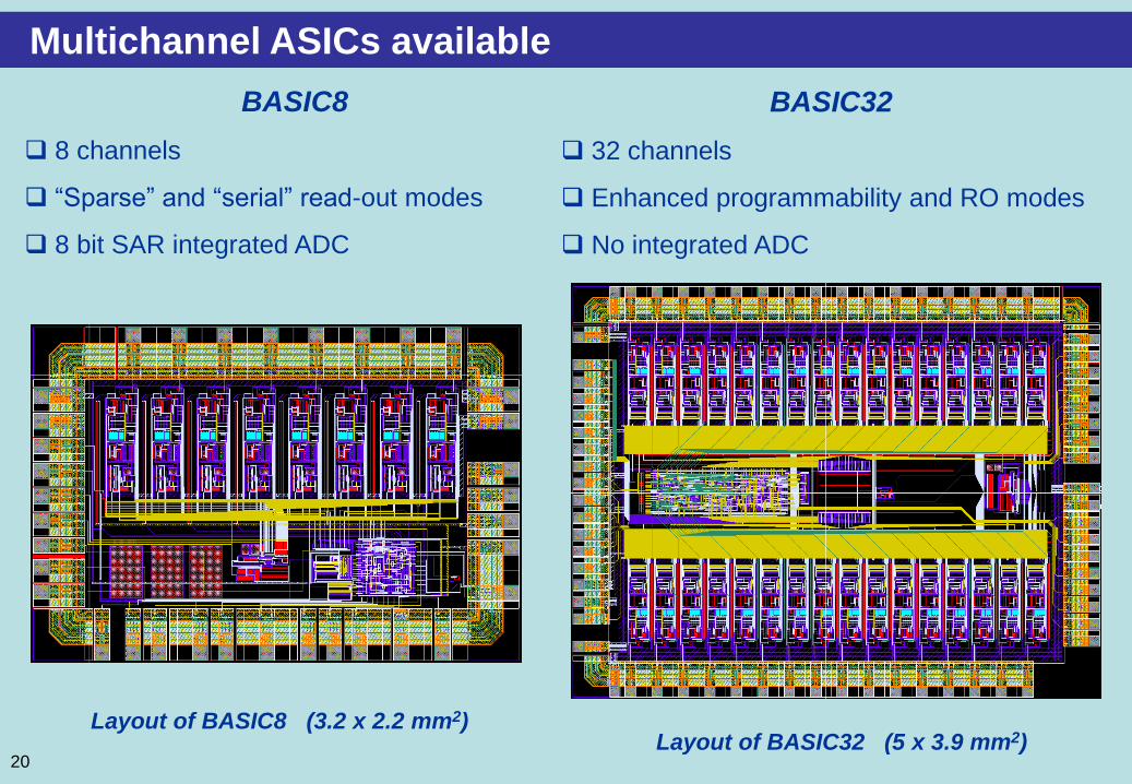
Multichannel ASICs available
Layout of BASIC32 (5 x 3.9 mm2) Layout of BASIC8 (3.2 x 2.2 mm2)
BASIC8
8 channels
“Sparse” and “serial” read-out modes
8 bit SAR integrated ADC
BASIC32
32 channels
Enhanced programmability and RO modes
No integrated ADC
20

BASIC32: block diagram
R
E
A
D
-
O
U
T
D
A
T
A
R
E
G
CONVERSION LOGIC
Channel
address
October 26, 2012 21

BASIC32: main features
Acquisition modes
Multiplexing, PD control and reset of the channels managed by the read-out logic
External read-out
External control of the PD’s
External channel addressing
Internal trigger (“fast-OR”)
External trigger }
Serial
Internal read-out
Sparse
Read-out logic
Multiplexer management
Fast-or management
Masking and reset of the channels
Conversion logic
ADC management
Data flow management
Coincidence management
External “coincidence” signal:
In internal read-out mode, the
acquisition is conditioned by this signal
Configuration logic
SPI interface
56-bit configuration word
Verification features
22
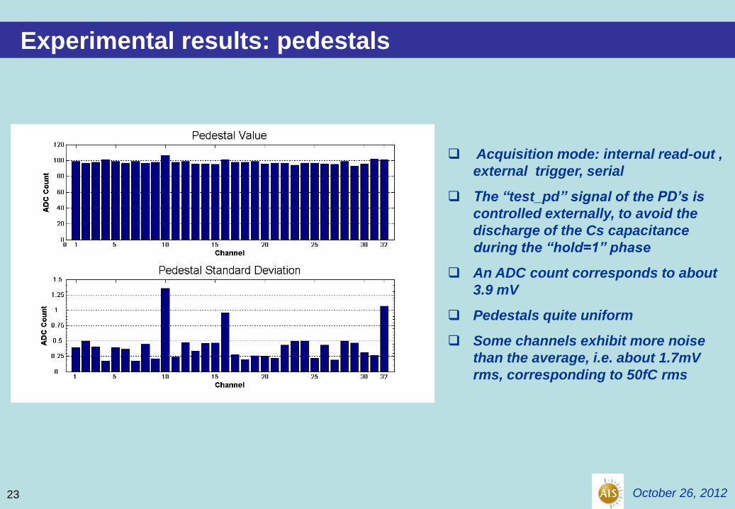
Experimental results: pedestals
Acquisition mode: internal read-out ,
external trigger, serial
The “test_pd” signal of the PD’s is
controlled externally, to avoid the
discharge of the Cs capacitance
during the “hold=1” phase
An ADC count corresponds to about
3.9 mV
Pedestals quite uniform
Some channels exhibit more noise
than the average, i.e. about 1.7mV
rms, corresponding to 50fC rms
October 26, 2012 23

Experimental results: injection capacitance, gain
CF 1PF 2PF 3PF
EXPECTED GAIN 100 50 33
MEASURED GAIN 94 47 33
Expected and measured values of the gain
DVOUT/Qin [mV/pC]
Fin
OUT
NCQ
V 1
DCharge to voltage gain
of the analog channel
Overall charge to voltage gain very close to the expected one (max. deviation 6%)
Max dynamic range 70pC @ CF=3pF (1% linearity error)
October 26, 2012 24

Experimental results: injection capacitance, timing
Measured standard deviation
smeas 130 ps
Intrinsic error of the measurement
setup
ssetup 60 ps
Resulting intrinsic timing accuracy
of the fast-OR signal
sint 115 ps
Timing accuracy of the fast-OR response vs the input pulse
October 26, 2012 25

Experimental results: coupling to SiPM+scintillator (I)
SiPMs from Hamamatsu a) 3600 micro-cells, 3x3mm2 , (gain = 7.5x10⁵ @ VBIAS=71.3V)
b) 782 micro-cells, 3.22x1.19mm2, (gain = 1.3x10⁵ @ VBIAS=71.2V)
SiPMs coupled to a small LYSO scintillator 3x3x10mm3
The SiPM+LYSO detector has been coupled to a channel of the ASIC and exposed to different
radiation sources:
176Lu (203keV and 307keV), 22Na (511keV), 137Cs (662keV), 57Co (122keV)
Hamamatsu SiPM coupled to the LYSO crystal Example of 137Cs spectrum ( 12% FWHM)
3x3mm2 SiPM
VBIAS = 70.2V
Gain = 33mV/pC
October 26, 2012 26
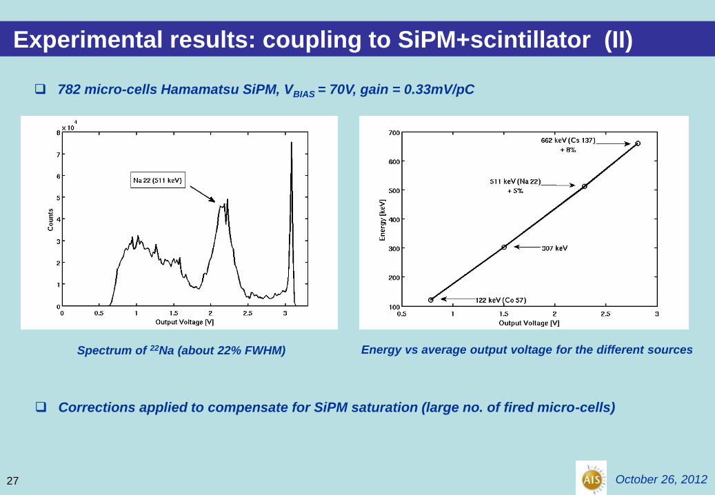
Experimental results: coupling to SiPM+scintillator (II)
782 micro-cells Hamamatsu SiPM, VBIAS = 70V, gain = 0.33mV/pC
Energy vs average output voltage for the different sources Spectrum of 22Na (about 22% FWHM)
Corrections applied to compensate for SiPM saturation (large no. of fired micro-cells)
October 26, 2012 27

Measurements of SiPM in coincidence with a PMT (I)
Measurement setup at CERN (courtesy of E. Chesi, A. Rudge and J. Seguinot)
Measurements taken in coincidence with a PMT
Very low event rate ( 1.9 Hz)
Signals acquired with an oscilloscope
Spectrum of 22Na spectrum very similar to the
one shown in the previous slide
(low threshold)
28
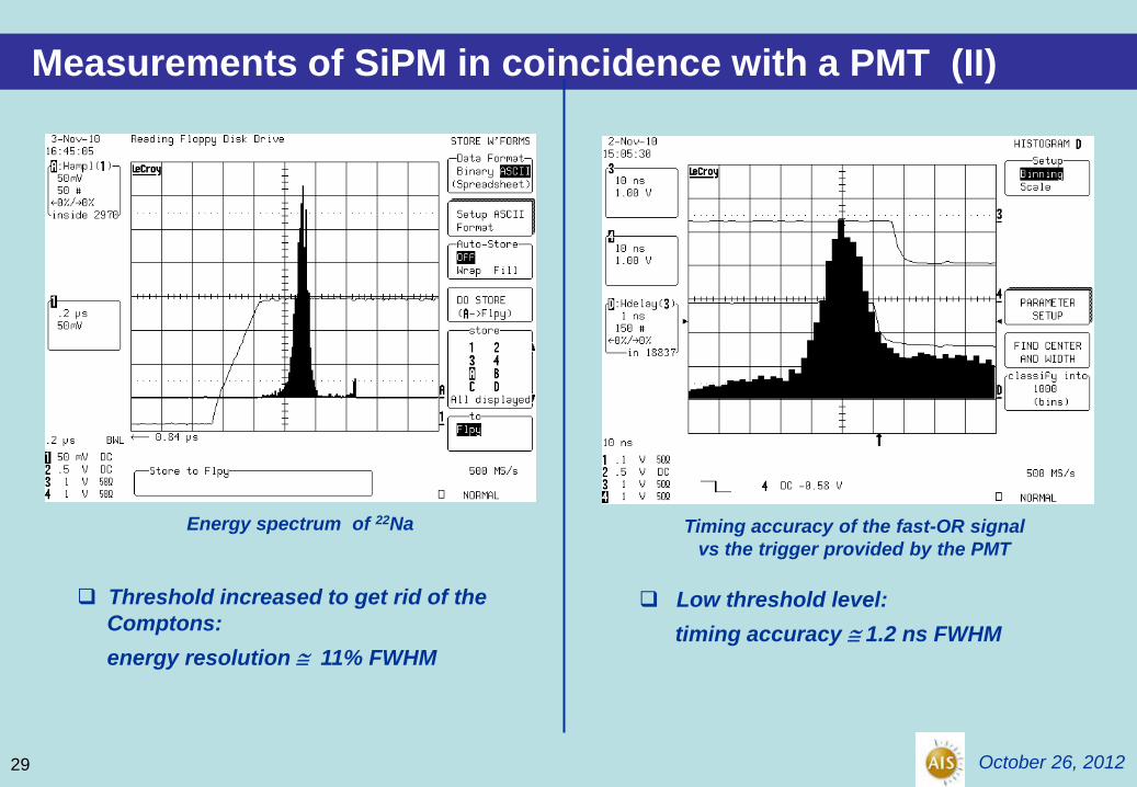
Measurements of SiPM in coincidence with a PMT (II)
Timing accuracy of the fast-OR signal
vs the trigger provided by the PMT
Low threshold level:
timing accuracy 1.2 ns FWHM
Energy spectrum of 22Na
Threshold increased to get rid of the
Comptons:
energy resolution 11% FWHM
October 26, 2012 29
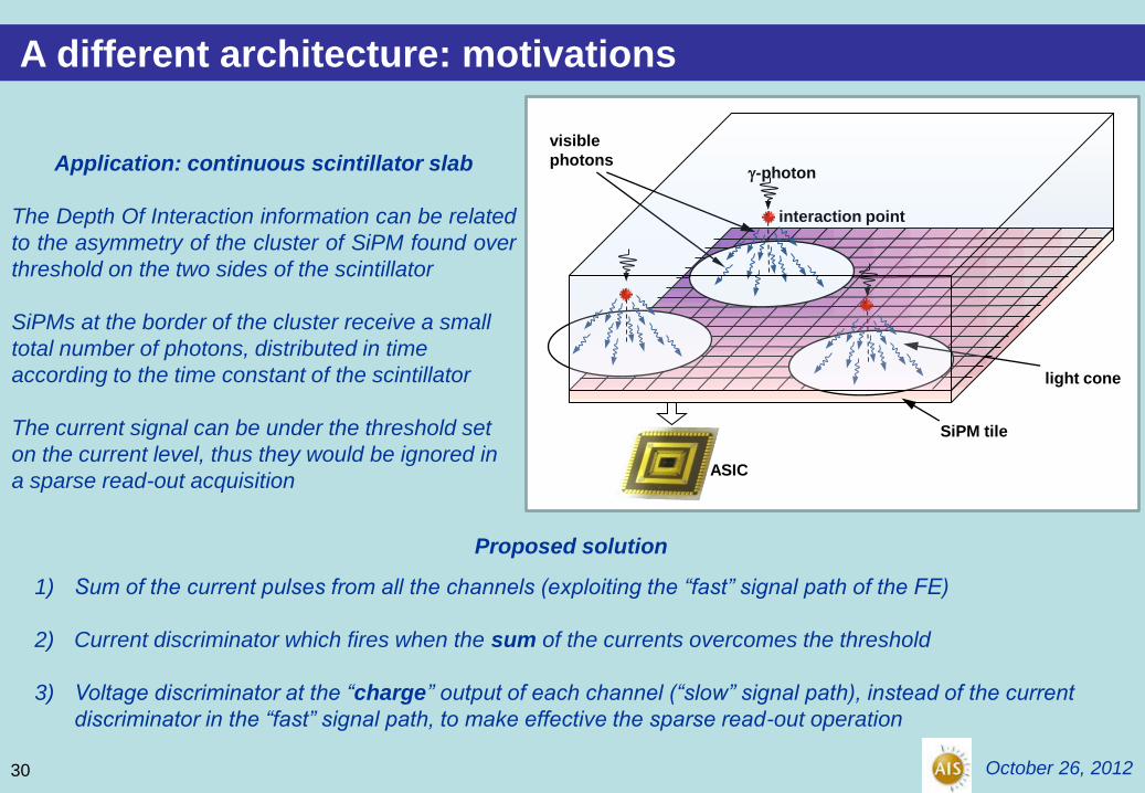
A different architecture: motivations
Application: continuous scintillator slab
The Depth Of Interaction information can be related
to the asymmetry of the cluster of SiPM found over
threshold on the two sides of the scintillator
SiPMs at the border of the cluster receive a small
total number of photons, distributed in time
according to the time constant of the scintillator
The current signal can be under the threshold set
on the current level, thus they would be ignored in
a sparse read-out acquisition
Proposed solution
1) Sum of the current pulses from all the channels (exploiting the “fast” signal path of the FE)
2) Current discriminator which fires when the sum of the currents overcomes the threshold
3) Voltage discriminator at the “charge” output of each channel (“slow” signal path), instead of the current
discriminator in the “fast” signal path, to make effective the sparse read-out operation
SiPM tile
ASIC
g-photon
interaction point
visible
photons
light cone
October 26, 2012 30

New proposed architecture
+
-
+
-
Vdd
+
-Ext.
bias
Ext.
bias
Ext.
bias
Cur_buf CSA PD
Cur_buf CSA PD
Cur_buf CSA PD
ch_0
ch_1
ch_31
Cur_disc
I_th V_th
V_th
V_th
To sparse
read-out
To sparse
read-out
To sparse
read-out
MUX Out_mux
(to ADC or external pad)
Summing circuit
Current sum
Fast trigger signal
from current sum
Slow trigger signal
from fast-OR
fast_OR
October 26, 2012 31
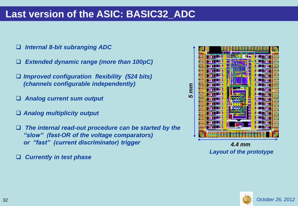
Last version of the ASIC: BASIC32_ADC
4.4 mm
5 m
m
Layout of the prototype
Internal 8-bit subranging ADC
Extended dynamic range (more than 100pC)
Improved configuration flexibility (524 bits)
(channels configurable independently)
Analog current sum output
Analog multiplicity output
The internal read-out procedure can be started by the
“slow” (fast-OR of the voltage comparators)
or “fast” (current discriminator) trigger
Currently in test phase
October 26, 2012 32
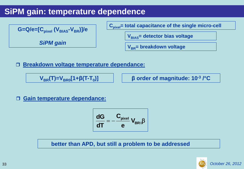
SiPM gain: temperature dependence
Cpixel= total capacitance of the single micro-cell G=Q/e=[Cpixel (VBIAS-VBR)]/e
SiPM gain
VBIAS= detector bias voltage
VBR= breakdown voltage
Breakdown voltage temperature dependance:
better than APD, but still a problem to be addressed
VBR(T)=VBR0[1+β(T-T0)] β order of magnitude: 10-3 /°C
Gain temperature dependance:
0BR
pixelV
e
C
dT
dG
October 26, 2012 33

Solutions proposed in the literature
Based on open loop techniques:
a. Measurement of parameter β
b. Measurement of the temperature (using a sensor)
c. SiPM bias voltage adjustment DVBIAS=DVBR(T)
Parameters , a and g must be known and/or controlled with good accuracy
VS(T)=V0[1+a(T-T0)]
October 26, 2012 34

New proposed solution
Closed loop technique:
a. A SiPM not exposed to incident photons (“blind” SiPM) is used as a temperature
sensor
b. Measurement of the average dark pulse amplitude VPEAK of the blind SiPM
(proportional to the gain)
c. Blind SiPM bias voltage automatically adjusted by a feedback loop to make VPEAK
(thus the gain) constant and equal to a reference value VREF
Main requirement: same for the blind SiPM and the active detectors
October 26, 2012 35

Experimental proof of principle
a. Single measurement cycle: VBIAS increased linearly on the bind SiPM until the
desired VPEAK (i.e. the required gain) is reached (VBIAS =VBIAS*)
b. Measurement cycles continuously applied : VBIAS* tracks the temperature variations and is
applied to the active SiPMs
October 26, 2012 36
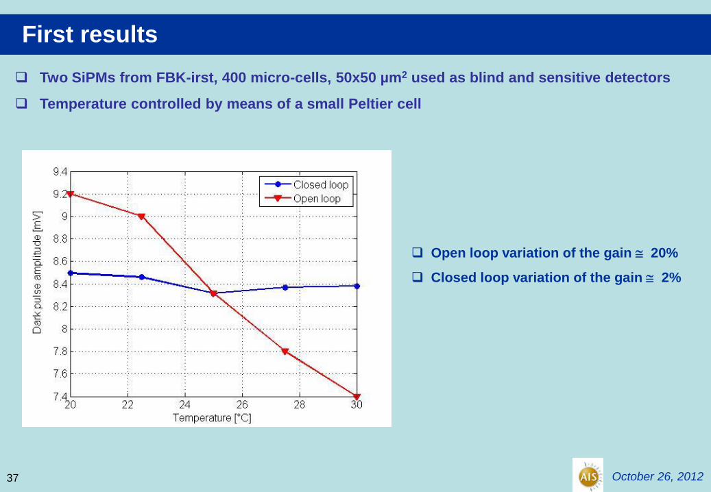
First results Two SiPMs from FBK-irst, 400 micro-cells, 50x50 µm2 used as blind and sensitive detectors
Temperature controlled by means of a small Peltier cell
Open loop variation of the gain 20%
Closed loop variation of the gain 2%
October 26, 2012 37

Application of BASIC in a PET prototype: small animal PET (Pisa)
Characterization of the last version of BASIC with modified architecture
Effective circuit implementation of the temperature compensation technique
Statistical modelling of the current pulse waveform produced by the system
scintillator + SiPM + FE electronics for timing accuracy evaluation
Design of a new SiGe ASIC with enhanced timing capabilities
Work in progress
October 26, 2012 38