integrated design for integrated photonics: from the...
TRANSCRIPT
Integrated design for integrated photonics:from the physical to the circuit level and back
Wim Bogaerts, Yanlu Li, Shibnath Pathak, Alfonso Ruocco, Martin Fiers,Antonio Ribeiro, Emmanuel Lambert, Pieter Dumon
Ghent University - imec, Photonics Research Group, Department of Information Technology,Center for Nano and Biophotonics, Sint-Pietersnieuwstraat 41, 9000 Gent, Belgium
ABSTRACT
Silicon photonics is maturing rapidly on a technology basis, but design challenges are still prevalent. We discussthese challenges and explain how design of photonic integrated circuits needs to be handled on both the circuitas on the physical level. We also present a number of tools based on the IPKISS design framework.
Keywords: Photonic Integrated Circuits, Design, Simulation
1. INTRODUCTION
Silicon Photonics is rapidly gaining industrial traction, the fabrication technology becomes more mature anddevice demonstrations start to meet functional specs for real-life applications. The scaling of silicon opticalwaveguides to submicron dimensions also opens the opportunity for very compact chips that can accommodateunprecedented levels of complexity in a photonic circuit. But at the same time, the submicron dimensions andhigh index contrast introduce low tolerances to fabrication variations. This combination of high complexity withlow tolerances sounds like a recipe for a low yield. And this is difficult to counter on the design side, because thedesign process for integrated photonics has not evolved as rapidly as the technology base for silicon photonics.
Photonic design is still very much a physical design activity, especially in silicon photonics, where the highrefractive index contrast makes most common approximations for optical simulations useless. Full-vectorialbrute-force electromagnetic number crunching of physical geometries is still the most applied design method forindividual building blocks,1–5 or alternatives based on mode expansion6,7 and propagation.8 These methodscannot scale up to large, complex circuits, which need to be designed at circuit level. But at this level, suitablesimulation tools are only just emerging.9–12 Such circuit simulators are based on behavioral models to efficientlysimulate many circuit elements.
As circuit simulators and physical simulators are generally based on very different principles, they are oftenused separately. However, for silicon photonics design, where there is still a very strong need for physicalsimulation while at the same time larger circuits need to be simulated, these two levels of simulation shouldbe more tightly integrated. For example, a circuit simulation might require a detailed physical simulation of acertain building block to establish the validity of a model or calculate the transmission. In an integrated designand simulation flow, such a simulation could be triggered automatically. At this moment, only a few tools offerthis capability in a limited way.11,13,14
Photonic design tools have historically evolved apart from the electronic design automation (EDA) ecosystem,but with the advent of silicon photonics this is also about to change. Silicon photonic circuits will, for mostapplications, require complex control circuitry, and at that point electronic-photonic codesign becomes a necessity,whether the photonic and electronic circuits are collocated on the same die or on separate chips. Electronic designframeworks rely very strongly on parametric building blocks (PCells), a concept which has also been introducedin photonic design environments13,15
We present IPKISS,16,17 a parametric design framework for photonic integrated circuits.16 It is a component-centric framework which allows the designer to perform several design and simulation activities from within the
Further author information: (Send correspondence to W.B.)W.B.: E-mail: [email protected], Telephone: +32 9 264 3324
Invited Paper
Integrated Optics: Physics and Simulations, edited by Pavel Cheben, Jirí Ctyroký, Iñigo Molina-Fernandez, Proc. of SPIE Vol. 8781, 878102 · © 2013 SPIE · CCC code: 0277-786X/13/$18
doi: 10.1117/12.2017761
Proc. of SPIE Vol. 8781 878102-1
Downloaded From: http://proceedings.spiedigitallibrary.org/ on 05/15/2013 Terms of Use: http://spiedl.org/terms
Physical designphysical simulationcomponent layoutcomponent models
/ $IIIMMINMUNIME
design flow
Circuit designnetlist, schematiccircuit simulation
Layoutplace- and -routecustom layouts
Verificationdesign rule checklayout -vs. schematic
tothefa b
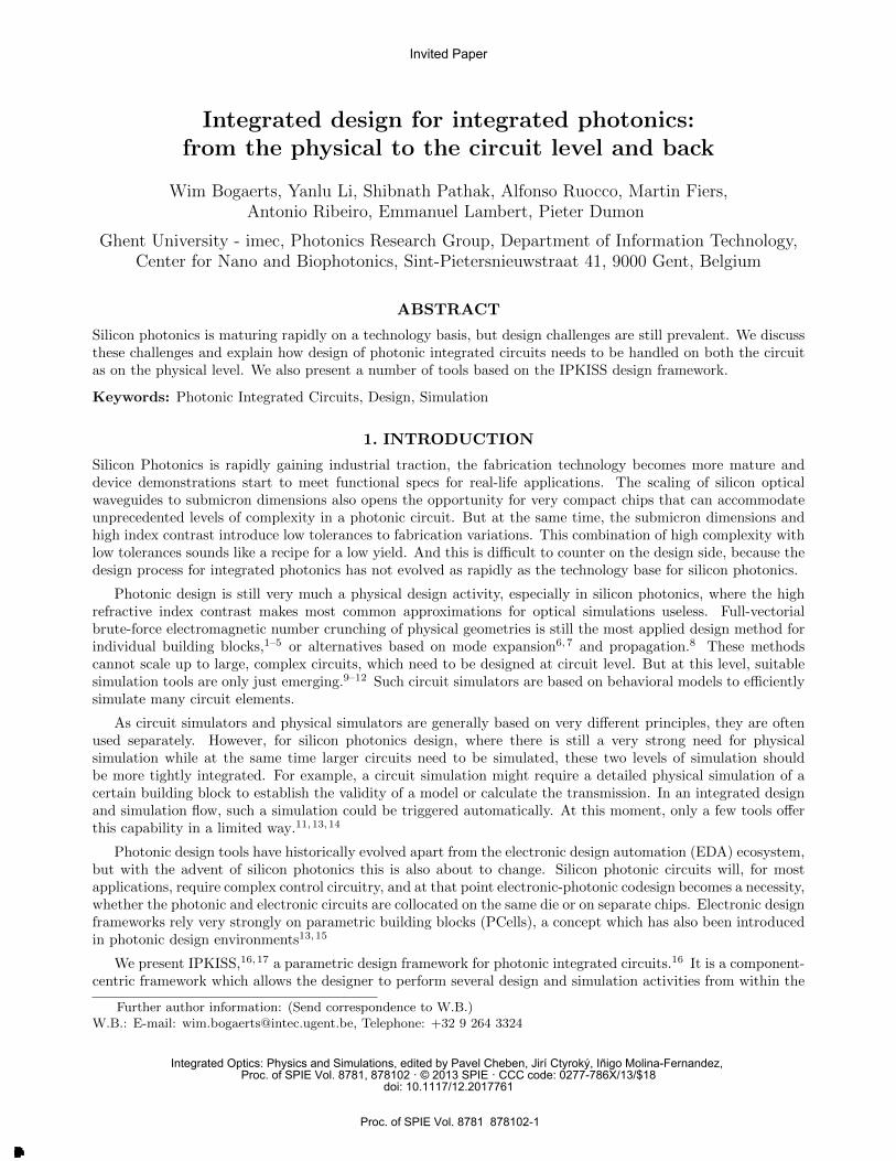
Figure 1. Design flow for photonic integrated circuits.
same component library, and generate different output based on the same component definition. As we willdiscuss further, we can define a component once in IPKISS, and from that definition launch an 2D or 3D FDTDsimulation, an eigenmode expansion simulation, a circuit simulation, but also generate a mask layout for thecomponent and the circuit. Also, integration with custom simulation tools and models is relatively easy, as theframework interface is open. This way, a bridge is laid between the physical design and the circuit design, andthe designer can combine the strengths of different methods.
In this paper, we will discuss how IPKISS can facilitate the design flow of silicon photonics. First, we willtake a closer look at the different steps taken in this design flow, from the physical design to the circuit leveland finally back to the physical layout and its verification. Then, we will discuss the IPKISS framework in moredetail and how it is used in each step of this process. Finally, we will illustrate the strength of this method witha number of challenging design examples.
2. SILICON PHOTONIC DESIGN FLOW
To design a photonic integrated circuit, most designers will have to go through at least 4 phases before the designcan be sent out for fabrication. This is illustrated in Fig. 1.
Component design First of all, individual building blocks need to be designed according to initial specifica-tions. This is typically a physical design step involving mask layout and electromagnetic modeling. Today,component design is still very much a part of actual photonic circuit design. It is expected however, that inthe future this part of the design flow will be largely done by the fab, which will use it to define standardcomponent for its design kit. Still, full-custom component design for circuits will still be an importantactivity in the foreseeable future.
Circuit design The designed components are linked together in a schematic, and the response of the resultingcircuit is simulated. Depending on the type of photonic components in the circuit and the targetedapplication, this simulation can become very complex. This is because photonic behavior has a richnessthat surpasses that of electronics, requiring the modeling of phase-coherent signals over a wide wavelengthrange.
Circuit layout The high-level description of the circuit is translated into a mask layout for fabrication. Photoniccomponents have a more complex layout that electronic building blocks. Photonic waveguides followcurvilinear shapes with smooth bends, and impose different requirements on alignment and pattern fidelitythan electronic designs.
Verification The layout is checked for violations of design rules, and whether it matches the functional de-scription of the circuit. For this design rule checking (DRC), verification tools from the electronics designworld are used,18 although some tools support DRC specifically for photonics.19 But these are not (yet)well equipped to handle the smooth curves of photonics. Also, extracting functional information and in-terconnectivity from a photonic layout (layout-vs-schematic or LVS) is very different than for an electroniclayout.
Proc. of SPIE Vol. 8781 878102-2
Downloaded From: http://proceedings.spiedigitallibrary.org/ on 05/15/2013 Terms of Use: http://spiedl.org/terms
As already explained in the introduction, these steps are usually not very well integrated for a photonic designflow, and often the designer will need to redo a significant part of the work to redefine components in differenttools. This makes such a design flow prone to casual errors due to wrongly copying design parameters betweendifferent steps in the flow. Still, some design tools do integrate some steps in the flow, such as a link betweenphysical and circuit simulation11,14 or between circuit simulation and layout.3,20
3. IPKISS: A PARAMETRIC DESIGN FRAMEWORK
IPKISS is a photonic design framework developed at Ghent University and imec. Its origins date back to 2001when research in silicon photonics exposed the needs for tools to generate complex waveguide circuit layouts ina parametric way (e.g. to generate designs with parameter sweeps on some circuit elements). At that point,the decision was made to implement this tool as a scripting framework in Python, because of the flexibility andreadability of the language and the availability of many high-performance scientific libraries.21 With IPKISS, thephotonics research group has generated hundreds of designs of silicon photonic integrated circuits, and a largelibrary of parametric building blocks was constructed, together with the layer settings to generate complex GDIIfiles. Since then, IPKISS has evolved from a flexible GDSII generator to a broader component-oriented designframework. At the core is a library manager that allows users to define parametric building blocks. Buildingblocks can be hierarchical, which means they can contain other ’child’ building blocks and connect them togetherinto a (sub)circuit. In fact, complete circuits are treated in much the same way as atomic building blocks whichdo not have children. To these building blocks, different representations (views) can be added. Mask layoutis only one of those. Other such views include an input-output ports, interconnectivity matrix (or netlist), 3Dgeometry, and interfaces to simulation tools for physical and circuit simulation.
IPKISS itself does not perform simulations, but the python scripting framework makes it easy to interfaceIPKISS to other simulators. The framework contains a set of generic interface layers to simulators, that canbe extended to match a specific tool. For example, there is a generic FDTD layer, which is then implementedfor MIT’s open-source MEEP simulator,1 but it could just as well be used for another FDTD simulator, eithercommercial or open source. Similarly, IPKISS interfaces with an in-house developed mode solver, but also withCAMFR, an eigenmode expansion tool.7 For circuit simulators IPKISS has a link to Caphe,9,22 a powerfultime and frequency domain optical circuit simulator, but the openness of the framework allows the use of othersimulators as well.
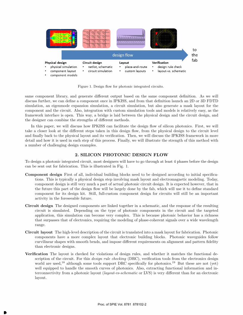
IPKISS itself manages the interaction between the views and the associated tools. This, way, views canbe made to depend on one another. One workflow which is predefined in IPKISS is illustrated in Fig. 2. Acomponent (here, a 3dB splitter based on a multi-mode interferometer) is defined with a number of parameters.This can be a predefined component, or a user-defined component. In this example, we need to define a masklayout for this component, consisting of a set of polygons on the correct layers, such that the component canbe fabricated with lithography. The definition of these layers is stored in a Technology File, which containsthe specifics of the fabrication technology. Base on this mask layout, IPKISS can now generate other views. Ifthe Technology file specifies a fabrication process, IPKISS can apply the fabrication flow to the mask layout,which results in a 3D distribution of materials. This built-in virtual fabrication engine generates an approximategeometry of material stacks, which cannot capture the full physics of the actual fabrication, but interfacingIPKISS to alternative (commercial) TCAD simulators is definitely possible (but not implemented at this time).The 3-D geometry can be used directly to define the simulation volume for a physical simulation. If the userhas also specified input and output ports, the simulation volume could be supplied with the necessary excitationsources and monitors at the inputs and outputs.
Based on this information, IPKISS can launch a physical simulation to extract the transmission from oneinput port to all outputs, and this simulation can be repeated (if needed) to extract a complete scatter matrix(S-matrix) of the component. the choice of physical simulation engine can depend on the component and couldinvolve mode-expansion based techniques or FDTD. Such simulations could be controlled by an optimizationalgorithm to tailor the response of a component.23 This is illustrated further in one of the examples. Theresulting S-matrix can also be used in a circuit model of the component and invoked when the component isused in a circuit simulator such as Caphe. These heavy physical simulations can be done in advance to extractand store such a circuit model, or they can be executed on demand when they are needed. The former can be
Proc. of SPIE Vol. 8781 878102-3
Downloaded From: http://proceedings.spiedigitallibrary.org/ on 05/15/2013 Terms of Use: http://spiedl.org/terms
(a) Mask layout
(b) 2D /3D geometry
Si 150nm
SiO2 2µm
i......unuuuuumnllnnnllll,l I i'
I I 1.1,11IIIIIII.Ii'.'.'........
LUrl.l.l.l rnln,rinntnn....n...
(d) FDTD simulation (Meep)
Figure 2. Views in IPKISS can be derived from one another. Example based on an multi-mode interferometer (MMI)for 3dB-splitting. (a) We can start from a mask layout (a) to generate a 2D of 3D material distribution (b) basedon fabrication information. This geometry can be exported to a refractive index distribution (c) for simulation in anelectromagnetic solver such as MEEP (d). From the output (e) a scatter matrix can be extracted.
desirable when many heavy simulations are needed, while the latter method is fine for occasional simulationsor when the component parameters exceed the limits of the available circuit model. In general, the physicalsimulation will significantly slow down the circuit simulation, especially when many components need to besimulated.
IPKISS does not provide a solution for verification of design rules. Technology settings allow the user tospecify design rules and use the preset values in the design to preempt design rule violations, but no hardchecking is performed by IPKISS. However, IPKISS supplies export routines to generate design rule check decksfor Calibre, the most widely used DRC engine for the verification of electronic IC designs.18
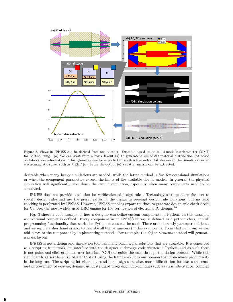
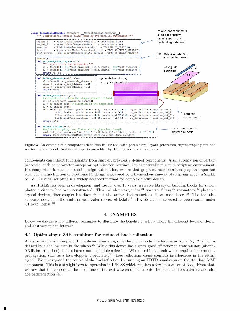
Fig. 3 shows a code example of how a designer can define custom components in Python. In this example,a directional coupler is defined. Every component in an IPKISS library is defined as a python class, and allprogramming functionality that works for Python classes can be used. These are inherently parametric objects,and we supply a shorthand syntax to describe all the parameters (in this example 5). From that point on, we canadd views to the component by implementing methods. For example, the define elements method will generatea mask layout.
IPKISS is not a design and simulation tool like many commercial solutions that are available. It is conceivedas a scripting framework: its interface with the designer is through code written in Python, and as such thereis not point-and-click graphical user interface (GUI) to guide the user through the design process. While thissignificantly raises the entry barrier to start using the framework, it is our opinion that it increases productivityin the long run. The scripting interface makes ad-hoc design somewhat more difficult, but facilitates the reuseand improvement of existing designs, using standard programming techniques such as class inheritance: complex
Proc. of SPIE Vol. 8781 878102-4
Downloaded From: http://proceedings.spiedigitallibrary.org/ on 05/15/2013 Terms of Use: http://spiedl.org/terms
saa0 S_}Smmm 8 dAn20Vara _Am a-3p _ _ldiva mRm
óIl o . -`ivT-C-' -- VvsWJU' o e6uroirP"eP9a:aa B o . egöa:ene.fP.opeiE Q:YdtA`6Lg o cAit12e` o e?'9aa4)Si o °ßi - ' _-^ ' °'.- ($'73#a!81t; o UMEerSa gggiggSM
DADM o a:im=- 1 - -Nç=- °,.q($:'Tar.81g o U2a2oUE,é'LL7:C5 EalZMILED
b-"-gaim, o an(§fl o 920:0o"'g,éy.Ll.k5 g32MEILEi1
BIS©@lag ç7 #iLrgt422D
mmmdhq;@pc0 p-{-zpwEsergraysimmmEfil a ((CA 0,00sLqZ0e9gEMEgdlo WE°noVI0 0e0qAV°EL:EgALUME@ a ECEZPQC(l®0-@o33Ms1,oPS CmIga -0e5ggaY,°QX=rza31D0:31= PS, PN
r.rst 'cm-eofismatiSallcao oiggE0gESo E0171 EG2geort. EfxgaeigqoSal"ìi £a EoZgorazr:Tffi' EQEMs; o E-120(Amp CaPEZEow:Lab°3 00EfgEgo10 Ea8:3011353 oaccao
generate layout usingwaveguide -4
component parameters1 line per propertydefaults from TECH(technology database)
intermediate calculations(can be cached for reuse)
waveguidedefinition®
ijft .- - -( 'o ^ - ore
1
PaulgamiS grgegtg2ormidtrad'ettx% sLSx100AEfiSa E@aE3i,eç7ag S get ..ue49ggeIl©E-Gl°Fc=-TÇ=¡(ÇD 0 d cgïdaaE-tc-=-eß o Eld°FaayVSiC=-+j®gm@ fa hInopei .1Por= togdtgEagi o 0470Do m:Y1r, o eIl1iD6pB0o tl7r'sk> o EiS,o6VY o
iSJ'-Eìt o EfiSCi] o `:+tiY. o OZ.1111 o (:t$ïfi3JS1 o E{ßlgoejfaY-.ó 21 osk_rS tagatiEm^ a WM -'t o o E-'ßWEOASWo fmTd7rsltlß] o ELigoarYlo4Jo,, =(ÇA°-4ií a EßQ41 o Fa::1r-a eßCC o r4=.a -s . oMur7i79Dariaggia ta)
onë6pfi-.1POr
rox2 ffi s , ase-= alga n gl,a4m LoE(. F4.v,3ratan 1=1 oapü Gd o 2,1 ° 04.0eZallECaMe©:?Ef ZoKga- c MistArßgD020maa Y1Q^3:ìï 4i.g o .5,=a 1 0,=.,
input andoutput ports
matrix modeetween all port
Figure 3. An example of a component definition in IPKISS, with parameters, layout generation, input/output ports andscatter matrix model. Additional aspects are added by defining additional functions.
components can inherit functionality from simpler, previously defined components. Also, automation of certainprocesses, such as parameter sweeps or optimization routines, comes naturally in a pure scripting environment.If a comparison is made electronic design automation, we see that graphical user interfaces play an importantrole, but a large fraction of electronic IC design is powered by a tremendous amount of scripting ’glue’ in SKILLor Tcl. As such, scripting is a widely accepted method for complex circuit design.
As IPKISS has been in development and use for over 10 years, a sizable library of building blocks for siliconphotonic circuits has been constructed. This includes waveguides,24 spectral filters,25 resonators,26 photoniccrystal devices, fiber coupler interfaces,27 but also active devices such as silicon modulators.28 The tool alsosupports design for the multi-project-wafer service ePIXfab.29 IPKISS can be accessed as open source underGPL-v2 license.16
4. EXAMPLES
Below we discuss a few different examples to illustrate the benefits of a flow where the different levels of designand abstraction can interact.
4.1 Optimizing a 3dB combiner for reduced back-reflection
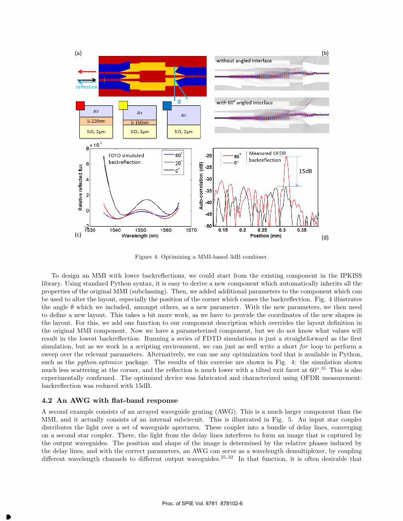
A first example is a simple 3dB combiner, consisting of a the multi-mode interferometer from Fig. 2, which isdefined by a shallow etch in the silicon.25 While this device has a quite good efficiency in transmission (about -0.3dB insertion loss), it does have a non-negligible reflection. When used in a circuit which requires bidirectionalpropagation, such as a laser-doppler vibrometer,30 these reflections cause spurious interferences in the returnsignal. We investigated the source of the backreflection by running an FDTD simulation on the standard MMIcomponent. This is a straightforward operation in IPKISS which requires a few lines of script code. From that,we saw that the corners at the beginning of the exit waveguide contribute the most to the scattering and alsothe backreflection (4).
Proc. of SPIE Vol. 8781 878102-5
Downloaded From: http://proceedings.spiedigitallibrary.org/ on 05/15/2013 Terms of Use: http://spiedl.org/terms
without angled interface
1 11111111111111111111(ill'"""""nnnuuuumnnnnippplllllllllilildd \
(a)
.11C-
Si 150nm
SiOi 2µm
FDTD simulatedbackreflection
1Air
SiOz 2µm
(b)
with 60° angled interface
No IIIIIIIIIIIII
PI
-50
60'0°
0.15 02
Measured OFDRbackreflection 4
l
I,025 0.3
Position (mm)
15dB
Figure 4. Optimizing a MMI-based 3dB combiner.
To design an MMI with lower backreflections, we could start from the existing component in the IPKISSlibrary. Using standard Python syntax, it is easy to derive a new component which automatically inherits all theproperties of the original MMI (subclassing). Then, we added additional parameters to the component which canbe used to alter the layout, especially the position of the corner which causes the backreflection. Fig. 4 illustratesthe angle θ which we included, amongst others, as a new parameter. With the new parameters, we then needto define a new layout. This takes a bit more work, as we have to provide the coordinates of the new shapes inthe layout. For this, we add one function to our component description which overrides the layout definition inthe original MMI component. Now we have a parameterized component, but we do not know what values willresult in the lowest backreflection. Running a series of FDTD simulations is just a straightforward as the firstsimulation, but as we work in a scripting environment, we can just as well write a short for loop to perform asweep over the relevant parameters. Alternatively, we can use any optimization tool that is available in Python,such as the python.optimize package. The results of this exercise are shown in Fig. 4: the simulation shownmuch less scattering at the corner, and the reflection is much lower with a tilted exit facet at 60◦.31 This is alsoexperimentally confirmed. The optimized device was fabricated and characterized using OFDR measurement:backreflection was reduced with 15dB.
4.2 An AWG with flat-band response
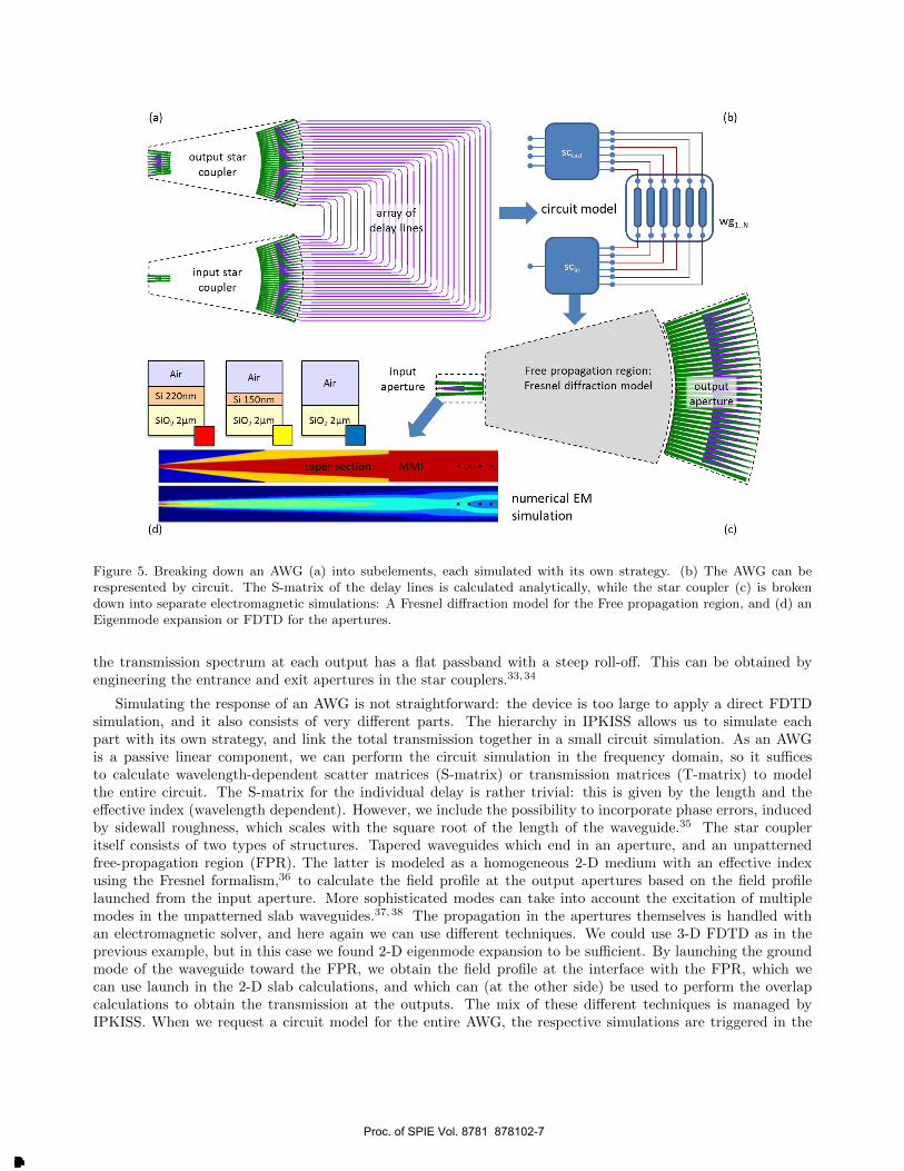
A second example consists of an arrayed waveguide grating (AWG). This is a much larger component than theMMI, and it actually consists of an internal subcircuit. This is illustrated in Fig. 5. An input star couplerdistributes the light over a set of waveguide apertures. These coupler into a bundle of delay lines, convergingon a second star coupler. There, the light from the delay lines interferes to form an image that is captured bythe output waveguides. The position and shape of the image is determined by the relative phases induced bythe delay lines, and with the correct parameters, an AWG can serve as a wavelength demultiplexer, by couplingdifferent wavelength channels to different output waveguides.25,32 In that function, it is often desirable that
Proc. of SPIE Vol. 8781 878102-6
Downloaded From: http://proceedings.spiedigitallibrary.org/ on 05/15/2013 Terms of Use: http://spiedl.org/terms
(a)
output starcoupler
-
I___ input starcoupler
circuit model
Air
SiO, 2µm
inputaperture
a(d)
FIFIF
Free propagation region:Fresnel diffraction model
(b)
Wg1..N
output raperture
numerical EMsimulation
(c)
Figure 5. Breaking down an AWG (a) into subelements, each simulated with its own strategy. (b) The AWG can berespresented by circuit. The S-matrix of the delay lines is calculated analytically, while the star coupler (c) is brokendown into separate electromagnetic simulations: A Fresnel diffraction model for the Free propagation region, and (d) anEigenmode expansion or FDTD for the apertures.
the transmission spectrum at each output has a flat passband with a steep roll-off. This can be obtained byengineering the entrance and exit apertures in the star couplers.33,34
Simulating the response of an AWG is not straightforward: the device is too large to apply a direct FDTDsimulation, and it also consists of very different parts. The hierarchy in IPKISS allows us to simulate eachpart with its own strategy, and link the total transmission together in a small circuit simulation. As an AWGis a passive linear component, we can perform the circuit simulation in the frequency domain, so it sufficesto calculate wavelength-dependent scatter matrices (S-matrix) or transmission matrices (T-matrix) to modelthe entire circuit. The S-matrix for the individual delay is rather trivial: this is given by the length and theeffective index (wavelength dependent). However, we include the possibility to incorporate phase errors, inducedby sidewall roughness, which scales with the square root of the length of the waveguide.35 The star coupleritself consists of two types of structures. Tapered waveguides which end in an aperture, and an unpatternedfree-propagation region (FPR). The latter is modeled as a homogeneous 2-D medium with an effective indexusing the Fresnel formalism,36 to calculate the field profile at the output apertures based on the field profilelaunched from the input aperture. More sophisticated modes can take into account the excitation of multiplemodes in the unpatterned slab waveguides.37,38 The propagation in the apertures themselves is handled withan electromagnetic solver, and here again we can use different techniques. We could use 3-D FDTD as in theprevious example, but in this case we found 2-D eigenmode expansion to be sufficient. By launching the groundmode of the waveguide toward the FPR, we obtain the field profile at the interface with the FPR, which wecan use launch in the 2-D slab calculations, and which can (at the other side) be used to perform the overlapcalculations to obtain the transmission at the outputs. The mix of these different techniques is managed byIPKISS. When we request a circuit model for the entire AWG, the respective simulations are triggered in the
Proc. of SPIE Vol. 8781 878102-7
Downloaded From: http://proceedings.spiedigitallibrary.org/ on 05/15/2013 Terms of Use: http://spiedl.org/terms
m
e
-20
1.5 1.51 1.52 1.53
Wavelength in pm1.54 (b
1.5 1.51 1.52
Wavelength in pm
1.43 1.
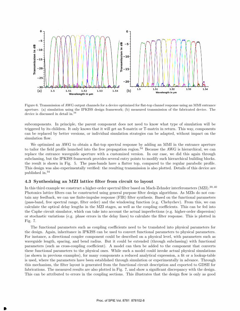
Figure 6. Transmission of AWG output channels for a device optimized for flat-top clannel response using an MMI entranceaperture. (a) simulation using the IPKISS design framework; (b) measured transmission of the fabricated device. Thedevice is discussed in detail in.34
subcomponents. In principle, the parent component does not need to know what type of simulation will betriggered by its children. It only knows that it will get an S-matrix or T-matrix in return. This way, componentscan be replaced by better versions, or individual simulation strategies can be adapted, without impact on thesimulation flow.
We optimized an AWG to obtain a flat-top spectral response by adding an MMI in the entrance apertureto tailor the field profile launched into the free propagation region.34 Because the AWG is hierarchical, we canreplace the entrance waveguide aperture with a customized version. In our case, we did this again throughsubclassing, but the IPKISS framework provides several entry points to modify such hierarchical building blocks.the result is shown in Fig. 5. The pass-bands have a flatter top, compared to the regular parabolic profile.This design was also experimentally verified: the resulting transmission is also plotted. Details of this device arepublished in.34
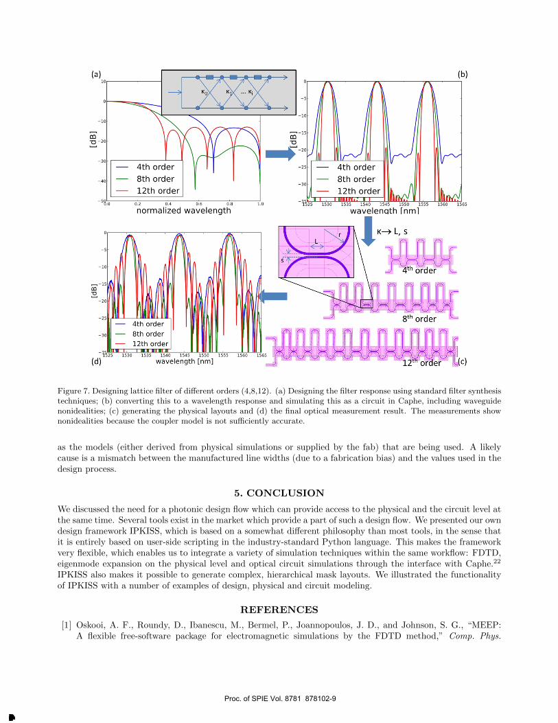
4.3 Synthesizing an MZI lattice filter from circuit to layout
In this third example we construct a higher-order spectral filter based on Mach-Zehnder interferometers (MZI).39,40
Photonics lattice filters can be constructed using general purpose filter design algorithms. As MZIs do not con-tain any feedback, we can use finite-impulse response (FIR) filter synthesis. Based on the functional parameters(pass-band, free spectral range, filter order) and the windowing function (e.g. Chebychev). From this, we cancalculate the optical delay lengths in the MZI stages, as well as the coupling coefficients. This can be fed intothe Caphe circuit simulator, which can take into account the actual imperfections (e.g. higher-order dispersion)or stochastic variations (e.g. phase errors in the delay lines) to calculate the filter response. This is plotted inFig. 7.
The functional parameters such as coupling coefficients need to be translated into physical parameters forthe design. Again, inheritance in IPKISS can be used to convert functional parameters to physical parameters.For instance, a directional coupler component could be described on a physical level, with parameters such aswaveguide length, spacing, and bend radius. But it could be extended (through subclassing) with functionalparameters (such as cross-coupling coefficient). A model can then be added to the component that convertsthese functional parameters to the physical ones. While such a model could invoke actual physical simulations(as shown in previous examples), for many components a reduced analytical expression, a fit or a lookup-tableis used, where the parameters have been established through simulation or experimentally in advance. Throughthis mechanism, the filter layout is generated from the functional circuit description and exported to GDSII forfabrications. The measured results are also plotted in Fig. 7, and show a significant discrepancy with the design.This can be attributed to errors in the coupling sections. This illustrates that the design flow is only as good
Proc. of SPIE Vol. 8781 878102-8
Downloaded From: http://proceedings.spiedigitallibrary.org/ on 05/15/2013 Terms of Use: http://spiedl.org/terms
(a)or
-->
(b)
4th order8th order
- 12th order30
02 o4 00 asnormalized wavelength
o
i1
11
I4th order8th order
5
order.5251 11530 ' 1535 1543 45 II 1550 1555
wavelength [nm]60
xtt4kxr I 'ec
;sI1'I I1. Ifl f1 f1 111 111 I
smxi arvrMmrc-; cig9,:di
Figure 7. Designing lattice filter of different orders (4,8,12). (a) Designing the filter response using standard filter synthesistechniques; (b) converting this to a wavelength response and simulating this as a circuit in Caphe, including waveguidenonidealities; (c) generating the physical layouts and (d) the final optical measurement result. The measurements shownonidealities because the coupler model is not sufficiently accurate.
as the models (either derived from physical simulations or supplied by the fab) that are being used. A likelycause is a mismatch between the manufactured line widths (due to a fabrication bias) and the values used in thedesign process.
5. CONCLUSION
We discussed the need for a photonic design flow which can provide access to the physical and the circuit level atthe same time. Several tools exist in the market which provide a part of such a design flow. We presented our owndesign framework IPKISS, which is based on a somewhat different philosophy than most tools, in the sense thatit is entirely based on user-side scripting in the industry-standard Python language. This makes the frameworkvery flexible, which enables us to integrate a variety of simulation techniques within the same workflow: FDTD,eigenmode expansion on the physical level and optical circuit simulations through the interface with Caphe.22
IPKISS also makes it possible to generate complex, hierarchical mask layouts. We illustrated the functionalityof IPKISS with a number of examples of design, physical and circuit modeling.
REFERENCES
[1] Oskooi, A. F., Roundy, D., Ibanescu, M., Bermel, P., Joannopoulos, J. D., and Johnson, S. G., “MEEP:A flexible free-software package for electromagnetic simulations by the FDTD method,” Comp. Phys.
Proc. of SPIE Vol. 8781 878102-9
Downloaded From: http://proceedings.spiedigitallibrary.org/ on 05/15/2013 Terms of Use: http://spiedl.org/terms

Comm. 181, 687–702 (January 2010).
[2] Lumerical Solutions, Inc., “Fdtd solutions.” http://www.lumerical.com/tcad-products/fdtd/.
[3] Phoenix BV, “Photonic design automation.” http://www.phoenixbv.com/.
[4] RSoft, “Photonics and network design software.” http://www.rsoftdesign.com/.
[5] Optiwave, “Design software for photonics.” http://www.optiwave.com.
[6] Photon Design, “FIMMProp-3D, a bidirectional optical propagation tool.”http://www.photond.com/products/fimmprop.htm.
[7] Bienstman, P. and Baets, R., “Optical modelling of photonic crystals and vcsels using eigenmode expansionand perfectly matched layers,” Opt. Quantum Electron. 33(4/5), 327 (2001).
[8] Scarmozzino, R., Gopinath, A., Pregla, R., and Helfert, S., “Numerical techniques for modeling guided-wavephotonic devices,” J. Sel. Top. Quantum Electron. 6(1), 150–162 (2000).
[9] Fiers, M., Van Vaerenbergh, T., Caluwaerts, K., Vande Ginste, D., Schrauwen, B., Dambre, J., and Bienst-man, P., “Time-domain and frequency-domain modeling of nonlinear optical components at the circuit-levelusing a node-based approach,” JOSA B 29(5), 896–900 (2012).
[10] Arellano, C., Mingaleev, S., Sokolov, E., Koltchanov, I., and Richter, A., “Time-and-frequency-domainmodeling (tfdm) of hybrid photonic integrated circuits,” in [SPIE OPTO ], 82650K–82650K, InternationalSociety for Optics and Photonics (2012).
[11] Lumerical Solutions, Inc., “Interconnect.” http://www.lumerical.com/tcad-products/interconnect/.
[12] Melati, D., Morichetti, F., Soares, F. M., and Melloni, A., “Building block based design of photonic in-tegrated circuits for generic photonic foundries,” in [Transparent Optical Networks (ICTON) 2012 ], 1–4,IEEE (2012).
[13] Bogaerts, W., Dumon, P., Fiers, M., Ribeiro, A., and Vanslembrouck, M., “Silicon photonics integrateddesign,” in [International Conference on Fibre Optics and Photonics ], Optical Society of America (2012).
[14] Arellano, C., Mingaleev, S., Koltchanov, I., Richter, A., Pomplun, J., Burger, S., and Schmidt, F., “Efficientdesign of photonic integrated circuits (pics) by combining device-and circuit-level simulation tools,” in [SPIEOPTO ], 862711–862711, International Society for Optics and Photonics (2013).
[15] Melati, D., Morichetti, F., Canciamilla, A., Roncelli, D., Soares, F., Bakker, A., and Melloni, A., “Vali-dation of the building-block-based approach for the design of photonic integrated circuits,” J. LightwaveTechnol. 30(23), 3610–3616 (2012).
[16] Ghent University - imec, “IPKISS parametric design framework.” http://www.ipkiss.org.
[17] Fiers, M., Lambert, E., Pathak, S., Dumon, P., Maes, B., Bienstman, P., and Bogaerts, W., “Improving thedesign cycle for nanophotonic components,” J. Comp. Sci. to be published (2013).
[18] Mentor Graphics, “Calibre - IC verification.” http://www.mentor.com.
[19] Design Workshop, “Dw2000 - photonic physical layout and verification software.”http://www.designw.com/PDA-Overview.php.
[20] Filarete, “ASPIC photonic circuit simulator.” http://www.aspicdesign.com/.
[21] Bienstman, P., Vanholme, L., Bogaerts, W., Dumon, P., and Vandersteegen, P., “Python in nanophotonicsresearch,” Comp. Sci. Eng. 9(3), 2801–2803 (2007).
[22] Ghent University - imec, “Caphe circuit simulator.” http://www.caphesim.eu.
[23] Bogaerts, W., Bradt, P., Vanholme, L., Bienstman, P., and Baets, R., “Closed-loop modeling of siliconnanophotonics from design to fabrication and back again,” Opt. Quantum Electron. 40, 801–811 (Sep.2008).
[24] Selvaraja, S., Jaenen, P., Bogaerts, W., Van Thourhout, D., Dumon, P., and Baets, R., “Fabrication ofphotonic wire and crystal circuits in silicon-on-insulator using 193nm optical lithography,” J. LightwaveTechnol. 27(18), 4076–4083 (2009).
[25] Bogaerts, W., Selvaraja, S., Dumon, P., Brouckaert, J., De Vos, K., Van Thourhout, D., and Baets, R.,“Silicon-on-insulator spectral filters fabricated with cmos technology,” J. Sel. Top. Quantum Electron. 16(1),33 –44 (2010).
[26] Bogaerts, W., De Heyn, P., Van Vaerenbergh, T., De Vos, K., Kumar Selvaraja, S., Claes, T., Dumon, P.,Bienstman, P., Van Thourhout, D., and Baets, R., “Silicon microring resonators,” Laser Photon. Rev. 6(1),47–73 (2012).
Proc. of SPIE Vol. 8781 878102-10
Downloaded From: http://proceedings.spiedigitallibrary.org/ on 05/15/2013 Terms of Use: http://spiedl.org/terms

[27] Taillaert, D., Bienstman, P., and Baets, R., “Compact efficient broadband grating coupler for silicon-on-insulator waveguides,” Opt. Lett. 29, 2749–2751 (December 2004).
[28] Hui, Y., Pantouvaki, M., Van Campenhout, J., Korn, D., Komorowska, K., Dumon, P., Li, Y., Verheyen,P., Absil, P., Alloatti, L., Hillerkuss, D., Leuthold, J., Baets, R., and Bogaerts, W., “Performance tradeoffbetween lateral and interdigitated doping patterns for high speed carrier-depletion based silicon modulators,”Opt. Express 20, 12926–12938 (Jun 2012).
[29] Dumon, P., Bogaerts, W., Baets, R., Fedeli, J.-M., and Fulbert, L., “Towards foundry approach for siliconphotonics: silicon photonics platform epixfab,” Electron. Lett. 45(12), 581–582 (2009).
[30] Li, Y., Verstuyft, S., Yurtsever, G., Keyvaninia, S., Roelkens, G., Van Thourhout, D., and Baets, R.,“Heterodyne laser doppler vibrometers integrated on silicon-on-insulator based on serrodyne thermo-opticfrequency shifters,” Appl. Opt. 52(10), 2145–2152 (2013).
[31] Li, Y. and Baets, R., “Improved multi-mode interferometers (mmis) on silicon-on-insulator with the opti-mized return loss and isolation,” in [16th Annual Symposium of the IEEE Photononics Benelux Chapter,Belgium ], (2011).
[32] Dragone, C., “An NxN optical multiplexer using a planar arrangement of two star couplers,” IEEE Photon.Technol. Lett. 3, 812–814 (Sept. 1991).
[33] Soole, J. B. D., Amersfoort, M., Leblanc, H., Andreadakis, N. C., Rajhel, A., Caneau, C., Bhat, R., Koza,M., Youtsey, C., and Adesida, I., “Use of multimode interference couplers to broaden the passband ofwavelength-dispersive integrated wdm filters,” Photon. Technol. Lett., 8(10), 1340–1342 (1996).
[34] Pathak, S., Vanslembrouck, M., Dumon, P., Van Thourhout, D., and Bogaerts, W., “Optimized silicon awgwith flattened spectral response using an mmi aperture,” J. Lightwave Technol. 31(1), 87–93 (2013).
[35] Goh, T., Suzuki, S., and Sugita, A., “Estimation of waveguide phase error in silica-based waveguides,” J.Lightwave Technol. 15(11), 2107–2113 (1997).
[36] Doerr, C. R., “Planar lightwave devices for wdm,” in [Optical Fiber Telecommunications ], Kaminow, I. P.and Li, T., eds., IV A, ch. 9, 405 – 476, Academic Press, ISBN 0-12-395172-0 (2002).
[37] Lycett, R. J., Gallagher, D., and Brulis, V., “Perfect chirped echelle grating wavelength multiplexor: Designand optimization,” IEEE Photon. J. 5(2), 2400123–2400123 (2013).
[38] Photon Design, “Epipprop, an echelle grating model.” http://www.photond.com/products/epipprop.htm.
[39] Bogaerts, W., Dumon, P., Van Thourhout, D., Taillaert, D., Jaenen, P., Wouters, J., Beckx, S., Wiaux, V.,and Baets, R., “Compact wavelength-selective functions in silicon-on-insulator photonic wires,” J. Sel. Top.Quantum Electron. 12, 1394–1401 (December 2006).
[40] Yamada, K., Shoji, T., Tsuchizawa, T., Watanabe, T., Takahashi, J., and Itabashi, S., “Silicon-wire-basedultrasmall lattice filters with wide free spectral ranges,” J. Sel. Topics Quantum Electron 11, 232–240 (2005).
Proc. of SPIE Vol. 8781 878102-11
Downloaded From: http://proceedings.spiedigitallibrary.org/ on 05/15/2013 Terms of Use: http://spiedl.org/terms