integrated dc-dc converter with ultra-low quiescent current
TRANSCRIPT

Integrated DC-DC Converter with Ultra-Low
Quiescent Currentby
Christine ChenS.B. EE, M.I.T, 2012
Submitted to the Department of Electrical Engineering and Computer
Sciencein partial fulfillment of the requirements for the degree of
Master of Engineering in Electrical Engineering
at the
MASSACHUSETTS INSTITUTE OF TECHNOLOGYJune 2013
@2013 Massachusetts Institute of Technology.
Author..................................... .... ..............Department of Electrical Engineering and Computer Science
May 2013
Certified by....................' Mark Vitunic
Design Section Leader, Linear TechnologyVI-A Thesis upervisor
Certified by..............Michael P. Whitaker
Design Engineer, Linear TechnologyVI-A Thesis Supervisor
Certified vy...................... . - --7..... .-David J. Perreault
Professor of Electrical Engineeringr4 fTS, s Supervisor
Accepted by............. .................Prof. Dennis M. Freeman
Chairman, Masters of Engineering Thesis Committee

2

Integrated DC-DC Converter with Ultra-Low Quiescent
Current
by
Christine Chen
Submitted to the Department of Electrical Engineering and Computer Scienceon May 21, 2013, in partial fulfillment of the
requirements for the degree ofMaster of Engineering in Electrical Engineering
Abstract
Based on the LTC3588, the design of a bandgap reference and a comparator for usein the control circuitry of DC-DC converter with an ultra-low quiescent current of150nA is presented here. Not only will this thesis discuss the challenges encounteredover the course of designing circuits to operate at such low current levels, but itwill also provide proof of concept silicon evaluation data of modified LTC3588 chipsdemonstrating that such low current operation is viable.
VI-A Thesis Supervisor: Mark VitunicTitle: Design Section Leader, Linear Technology
VI-A Thesis Supervisor: Michael P. WhitakerTitle: Design Engineer, Linear Technology
Thesis Supervisor: David J. PerreaultTitle: Professor of Electrical Engineering
3

4

Acknowledgments
I am grateful to Linear Technology Corporation for having the opportunity to work
on this project for my thesis research. In particular, I would like to especially thank
Sam Nork for his endless support and advice throughout my entire VI-A experience
with the LTC at the Boston Design Center. I would also like to thank Mark Vitunic
and Mike Whitaker for being such wonderful thesis supervisors. There was never a
dull moment working with them, and I always came away with some new piece of
information after every pow-wow. I would like to thank Professor David Perreault
for his help and guidance over the course of this thesis research.
I would also like to recognize Victor Fluere for all his infinite wisdom about
bandgap circuits, Ron Swinnich for always being able to fix my evaluation boards
even when I did not think it was possible, and Aspiyan Gazder for his brainstorming
help and advice over the course of this project. Special thanks to my Linear family,
including but not limited to Wendi Rieb, Eko Lisuwandi, and John Fiorenza, for
making my experience working at the Boston Design Center such a wonderful one. I
would especially like to thank Thilani Bogoda for being such an awesome roommate
and source of advice and support when I needed it.
My heart goes out to the amazing people I met here at MIT, who have seen
me at my best and my worst and never judged me for any of it: Alicia Erwin,
Hilary Monaco, Bridget Wall, Isabella Lubin, Vamsi Aribindi, Alejandro Arambula,
and William Chow. Likewise, many thanks go out to Ted Shinta, Mauri Laitinen,
and Bruce Kawanami for being such great teachers and sources of inspiration and
encouragement on my way to MIT.
Lastly, I would like to thank my family without whom I would not be where I am
today. I am forever grateful for my parents for their support and encouragement on
the path that I have taken and for always believing in me even when I did not. Their
infinite patience with me is not something I have always appreciated, but recognize
now with sincere gratitude. Thank you so much for letting me find my own way and
make my own mistakes so that I could learn from them.
5

6

Contents
1 Introduction
1.1 Prior Work . . . . .
1.2 Proposed Work .
2 System Overview
2.1 System Operation and Analysis . . . .
2.1.1 The Sleep State . . . . . . . . .
2.1.2 The Active State . . . . . . . .
2.2 Figures of Merit . . . . . . . . . . . . .
2.2.1 Line and Load Regulation . . .
2.2.2 Efficiency . . . . . . . . . . . .
2.2.3 Output Voltage Ripple . . . . .
2.3 Proof of Concept . . . . . . . . . . . .
2.3.1 Quiescent Current Modifications
2.3.2 Other Modifications . . . . . .
2.3.3 Weak Bias Blocks . . . . . . . .
2.3.4 Figure of Merit Evaluation . . .
2.3.5 Summary . . . . . . . . . . . .
3 Bandgap Reference
3.1 Theory of Operation . . . . . . . . . . . . . . . . . . . . . . . . . . .
3.1.1 Widlar Cell . . . . . . . . . . . . . . . . . . . . . . . . . . . .
3.1.2 Feedback and AC Stability . . . . . . . . . . . . . . . . . . . .
7
17
17
. . . . . . . . . . . . . . . . . . . . . 18
19
.... ....... 19
. . . . . . . . . . . 20
. . . . . . . . . . . 20
. . . . . . . . . . . 21
. . . . . . . . . . . 21
. . . . . . . . . . . 22
. . . . . . . . . . . 22
. . . . . . . . . . . 23
. . . . . . . . . . . 23
. . . . . . . . . . . 24
. . . . . . . . . . . 26
. . . . . . . . . . . 26
. . . . . . 28
29
29
31
32

3.2 Design Variations and Non-Idealities . . . . . . . . . . . . .
3.2.1 Bipolar 3 Variation . . . . . . . . . . . . . . . . . . .
3.2.2 Emitter Area Ratio . . . . . . . . . . . . . . . . . . .
3.2.3 Collector-Substrate Leakage at High Temperatures
3.2.4 Layout and Matching Techniques . . . . . . . . . . .
3.3 Start-up Circuit . . . . . . . . . . . . . . . . . . . . . . . . .
3.3.1 Supply Voltage Dependence . . . . . . . . . . . . . .
3.3.2 Final Design . . . . . . . . . . . . . . . . . . . . . . .
3.4 Trim Range and the ZTC Voltage . . . . . . . . . . . . . . .
3.5 Bandgap Ready and Undervoltage Lockout Signals . . . . .
3.5.1 Bandgap Ready Circuitry . . . . . . . . . . . . . . .
3.5.2 UVLO Signal Circuitry . . . . . . . . . . . . . . . . .
3.5.3 Combining the Bandgap Ready and UVLO Signals .
3.5.4 Final Design Integration . . . . . . . . . . . . . . . .
3.6 Proof of Concept . . . . . . . . . . . . . . . . . . . . . . . .
3.6.1 Measurement Setup . . . . . . . . . . . . . . . . . . .
3.6.2 Measurement Data and Analysis . . . . . . . . . . . .
3.7 Final Design . . . . . . . . . . . . . . . . . . . . . . . . . . .
3.7.1 Schematics . . . . . . . . . . . . . . . . . . . . . . . .
3.7.2 Simulation Results . . . . . . . . . . . . . . . . . . .
4 Sleep Comparator
4.1 Design Considerations . . . . . . . . .
4.2 BJT and MOS Device Characteristics .
4.2.1 MOS in Subthreshold . . . . . .
4.2.2 Differential Pairs . . . . . . . .
4.3 Hysteresis . . . . . . . . . . . . . . . .
4.3.1 DC Hysteresis . . . . . . . . . .
4.3.2 AC Hysteresis . . . . . . . . . .
4.4 Adaptive Biasing . . . . . . . . . . . .
8
33
33
38
39
41
42
43
45
46
47
47
50
51
56
59
59
60
63
63
64
67
. . . . . . . . . . . . . . . . . 6 7
. . . . . . . . . . . . . . . . . 6 8
. . . . . . . . . . . . . . . . . 6 8
. . . . . . . . . . . . . . . . . 6 9
. . . . . . . . . . . . . . . . . 7 2
. . . . . . . . . . . . . . . . . 7 3
. . . . . . . . . . . . . . . . . 7 4
. . . . . . . . . . . . . . . . . 7 4
4.5 Gain per Stage . . . . . . . .
4.6 Topology Comparison.....
4.6.1 Topology I . . . . . . .
4.6.2 Topology II . . . . . .
4.6.3 Topology III . . . . . .
4.6.4 Topology IV ......
4.6.5 Topology V . . . . . .
4.6.6 Simulation Results . .
4.7 Proof of Concept . . . . . . .
4.7.1 Measurement Setup . .
4.7.2 Measurement Data and
4.8 Final Design . . . . . . . . . .
4.8.1 Schematic . . . . . . .
4.8.2 Current Bias Leg . . .
4.8.3 Simulated Results . . .
5 Conclusion
5.1 Combined Simulated Results
5.2 Recap and Future Work . . .
Analysis
75
76
76
77
78
79
79
81
81
81
83
87
87
87
88
89
89
89
9
. . . . . . . . . . . . . . . . . . . . . .
. . . . . . . . . . . . . . . . . . . . . .

10

List of Figures
2-1 LTC3588 Block Diagram [5] . . . . . . . . . . . . . . . . . . . . . . . 19
2-2 Buck Converter Topology . . . . . . . . . . . . . . . . . . . . . . . . 20
2-3 Disabled Blocks in LTC3588 Modifications [5] . . . . . . . . . . . . . 24
2-4 Pin Re-purposing in LTC3588 Modifications . . . . . . . . . . . . . . 25
2-5 Line Regulation with Ct=100pF . . . . . . . . . . . . . . . . . . . . 26
2-6 Load Regulation Ct=100pF . . . . . . . . . . . . . . . . . . . . . . 27
2-7 Efficiency Curve for V,.=1.8V . . . . . . . . . . . . . . . . . . . . . . 28
3-1 Summation of CTAT and PTAT Voltages [8] . . . . . . . . . . . . . . 29
3-2 Producing AVBE with two Bipolar Transistors . . . . . . . . . . . . . 30
3-3 Graphical Analysis of the Intersection of Eq. 3-2 and Eq. 3-3 . . . . . 31
3-4 Widlar Bandgap Cell where m>0 . . . . . . . . . . . . . . . . . . . . 32
3-5 Modified Feedback Circuit . . . . . . . . . . . . . . . . . . . . . . . . 33
3-6 8 as a function of the Collector Current [9] . . . . . . . . . . . . . . . 34
3-7 Gummel Plot for the Base and Collector Currents [10] . . . . . . . . 35
3-8 Addition of R, . . . . . . . . . . . . . . . . . . . . . . . . . . . . . . 36
3-9 Splitting of RE such that RE=RE1+RE2 . . . . . . . . - -. . . . 37
3-10 Gain Analysis . . . . . . . . . . . . . . . . . . . . . . . . . . . . . . . 38
3-11 3-D Representation of Base-Emitter Junction [9] . . . . . . . . . . . . 39
3-12 Temperature Dependence of Collector-Substrate Leakage . . . . . . . 40
3-13 Equalizing Collector-Substrate Current Leakage . . . . . . . . . . . . 41
3-14 Sample Start-up Circuit . . . . . . . . . . . . . . . . . . . . . . . . . 42
3-15 PMOS Cross Sections [13] . . . . . . . . . . . . . . . . . . . . . . . . 43
11

3-16 I-V Characteristics of Depletion Mode PMOS . . . . . . . . . . . . . 44
3-17 Start-up Leg with Self-Regulating Depletion Mode PMOS Current Source 44
3-18 Start-up Leg Current as a function of Supply Voltage for RST = 320MQ 45
3-19 Trim Resistors . . . . . . . . . . . . . . . . . . . . . . . . . . . . . . . 46
3-20 Bandgap Ready Comparator Topology #1 . . . . . . . . . . . . . . . 48
3-21 Supply Voltage DC Sweep Simulation Results for Topology #1 . . . . 48
3-22 Bandgap Ready Comparator Topology #2 . . . . . . . . . . . . . . . 49
3-23 Supply Voltage DC Sweep Simulation Results for Topology #2 . . . . 49
3-24 Bandgap Circuit Dependent UVLO Signal Circuit . . . . . . . . . . . 50
3-25 Bandgap Inspired UVLO Signal Circuit where 'VSUPPLYMIN = VREF 51
3-26 Bandgap Ready Circuit Supply Voltage DC Sweep Simulation for Var-
ious RBGR -.. . ................................... .... 52
3-27 Bandgap Ready Topology Variation #1 . . . . . . . . . . . . . . . . . 53
3-28 Bandgap Ready Topology Variation #1 Supply Voltage DC Sweep Sim-
ulation . . . . . . . . . . . . . . . . . . . . . . . . . . . . . . . . . . . 53
3-29 Bandgap Ready Topology Variation #2 . . . . . . . . . . . . . . . . . 54
3-30 Bandgap Ready Topology Variation #2 Supply Voltage DC Sweep Sim-
ulation . . . . . . . . . . . . . . . . . . . . . . . . . . . . . . . . . . . 54
3-31 UVLO Signal Circuit with Modified Bandgap Start-up Leg . . . . . . 55
3-32 VGS and VBE Temperature Coefficients for 5nA of Drain and Collector
Bias Currents . . . . . . . . . . . . . . . . . . . . . . . . . . . . . . . 56
3-33 UVLO Signal Circuit . . . . . . . . . . . . . . . . . . . . . . . . . . . 57
3-34 Evaluation Board . . . . . . . . . . . . . . . . . . . . . . . . . . . . . 60
3-35 Measured Untrimmed Reference Voltage with VSUPPLY=3.5V . . . . 60
3-36 Measured Trimmed Reference Voltage with VSUPPLY=3.5V . . . . . . 61
3-37 Simulated Reference Voltage . . . . . . . . . . . . . . . . . . . . . . . 62
3-38 Untrimmed Reference Voltage with Varying Supply Voltage . . . . . . 63
3-39 Bandgap Circuit . . . . . . . . . . . . . . . . . . . . . . . . . . . . . 63
3-40 Bandgap Trim Network . . . . . . . . . . . . . . . . . . . . . . . . . . 64
3-41 UVLO Signal Circuit . . . . . . . . . . . . . . . . . . . . . . . . . . . 64
12

3-42 Simulated Bandgap Reference Voltage over Temperature at VSUPPLY =
5V ....... .....................................
3-43 Simulated UVLO Signal over Supply Voltage . . . . . . . . . . . . . .
4-1 Base Current Cancellation Technique . . . . . . . . . . . . . . . . . .
4-2 Bipolar Device Cross Section [14] . . . . . . . . . . . . . . . . . . . .
4-3 MOS Device Cross Section[14] . . . . . . . . . . . . . . . . . . . . . .
4-4 Two Stage Comparator with AC and DC Hysteresis Circuitry . . . .
4-5 Two Stage Comparator with Adaptive Biasing . . . . . . . . . . . . .
4-6 Topology I . . . . . . . . . . . . . . . . . . . . . . . . . . . . . . . . .
4-7 Topology II . . . . . . . . . . . . . . . . . . . . . . . . . . . . . . . .
4-8 Topology III where I, = 9I . . . . . . . . . . . . . . . . . . . . . . .
4-9 Topology IV . . . . . . . . . . . . . . . . . . . . . . . . . . . . . . . .
4-10 Topology V . . . . . . . . . . . . . . . . . . . . . . . . . . . . . . . .
4-11 Measurement Definitions . . . . . . . . . . . . . . . . . . . . . . . . .
4-12 QFN Evaluation Board for Single Part . . . . . . . . . . . . . . . . .
4-13 Large QFN Evaluation Board . . . . . . . . . . . . . . . . . . . . . .
4-14 Output Ripple as a Function of Load Current . . . . . . . . . . . . .
4-15 Comparison of Output Ripple for Various Capacitors for EXP13 . . .
4-16 Comparison of Output Ripple with C, = 22pF . . . . . . . . . . . .
4-17 Comparison of Output Ripple for Various Quiescent Current Levels
and Output Capacitors . . . . . . . . . . . . . . . . . . . . . . . . . .
4-18 Sleep Comparator . . . . . . . . . . . . . . . . . . . . . . . . . . . . .
13
65
65
70
71
72
73
75
76
77
78
79
80
81
82
82
83
84
85
86
87

14

List of Tables
1.1 Specifications for several current Linear Technology Switching Con-
verters and the Proposed Converter [2][3][4][5][6] . . . . . . . . . . . . 18
2.1 LTC3588 Experiment Variations . . . . . . . . . . . . . . . . . . . . . 23
3.1 Key Bandgap and UVLO Simulation Data . . . . . . . . . . . . . . . 65
4.1 npn and pnp Junction Capacitances at Zero Bias . . . . . . . . . . . 71
4.2 NMOS and PMOS Parasitic Capacitances at Zero Bias . . . . . . . . 72
4.3 Comparison of Propagation Delay and Output Ripple for Various Sleep
Comparator Topologies with VSUPPLY=3.5V, Cot=100pF, ILOAD=5OmA 81
4.4 Labeled vs. Actual Capacitance Values . . . . . . . . . . . . . . . . . 85
4.5 Sleep Comparator Simulation Data with VSUPPLY=5V, Cot=100pF,
ILOAD=5OmA . . . . . . . . . . . . . . . . . . . . . . . . . . . . . . . 88
5.1 Sleep Comparator Measurements with Bandgap Circuit with VSUPPLY=3.5V,
Cot=100ptF, and ILOAD=5OmA . . . . . . . . . . . . . . . . . . . . . 89
15

16

Chapter 1
Introduction
In a world increasingly concerned with maximization of device lifetimes, demand for
highly efficient DC-DC converters with ultra-low nominal operating current exists
across a variety of industries. In particular, such converters find specific applicability
in both remote battery-based systems where changing the battery can be especially
troublesome and in portable battery-based systems where constantly changing the
battery can become costly and inconvenient.
Applications for such converters predominately include sensors and biomedical
devices. For example, with the advent of new low power communication protocols,
wireless sensors simply do not need to consume very much power at all. If such
sensors were monitoring a factory production line, replacing the batteries powering
such sensors necessitates a costly partial or complete shutdown in production.
In biomedical applications, implanted medical devices such as pacemakers and
cochlear implants already operate at very low energy levels [1]. With a highly efficient
switching converter with low operating current, these devices can extend their battery
lives or increase the on-board computational power for the same battery life.
1.1 Prior Work
The demand for and benefits of highly efficient DC-DC converters that have a low
quiescent current are reflected in the rise in popularity of micropower converters.
17

Related research has also been conducted in previous theses on lowering quiescent
current in switching converters (Gardner, MIT, 2008) as well as conference papers
on designing converters and regulators for portable applications (Xiao, UC Berkeley,
2003). Commercially, many switching converters operate with a quiescent current in
the single digit pA range and are available for a range of input and output voltages
and load currents.
Part VIN Range (V) VOUT Range (V) IOUT,MAx (A) ISUPPLY (yA)LT3975 4 - 42 3.2 - 16 2.5 2.7LT3971 4.3-38 1.19-30 1.2 2.1
LTC3103 2.5 - 15 0.6 - 13.8 0.3 1.8LTC3588 2.7 - 20 1.8 - 3.6 0.1 0.95LTC3388 2.7 - 20 1.2 - 5 0.05 0.82
Proposed 1.8 - 5 1.8 - 3.6 0.1 < 0.150
Table 1.1: Specifications for several current Linear Technology Switching Convertersand the Proposed Converter [2] [3] [4] [5] [6]
1.2 Proposed Work
The focus of the work presented here is to push the quiescent current even lower and
design a low voltage, high efficiency switching converter with an ultra-low quiescent
current of less than 150nA, as seen in Table 1-1. Based on the LTC3588, a piezoelectric
energy harvesting buck converter with a no-load quiescent current of 950nA, the
proposed converter will operate with a similar hysteretic control scheme to maintain
high efficiency.
Reaching the substantially lower quiescent current levels proposed here requires
the re-design of two of the main operating blocks in the LTC3588 system, the bandgap
and sleep comparator circuits. To do this effectively, the effects of low current oper-
ation were first evaluated in modified versions of the LTC3588 fabricated with lower
operating currents. The evaluation results then informed the strategies used in the
low current design of the bandgap and sleep comparator blocks.
18

Chapter 2
System Overview
Although the stated low quiescent current objective is achieved through the re-design
of various blocks, the primary functionality of the blocks and the connections between
the blocks remain largely unchanged. As a result, the converter system presented here
will still possess the same overall control scheme as that in the LTC3588.
2.1 System Operation and Analysis
V5 FM
20VW
COM
G
REF~t VowT
01,00COWPR 1M PO
Figure 2-1: LTC3588 Block Diagram [5]
19

The relevant control blocks that determine the system operational state are marked
in the block diagram of Figure 2-1. First, the undervoltage (UVLO) block determines
the on-off state of the entire system based on a minimum input supply voltage. If this
minimum is met, then the result of a comparison between the bandgap voltage and a
preselected fraction of the output voltage decides whether or not the buck converter
is active. Internal to the converter itself is a boundary mode control scheme (not
shown in detail) that generates the switching function and thus sets the frequency of
operation based on the output inductance.
When the converter is on, called the active state, the sleep comparator checks to
see if the output voltage has reached regulation yet, whereas in the sleep state when
the converter is off, the sleep comparator checks to see if the output voltage has fallen
out of regulation. Regardless of the converter state, the UVLO continues to track
the supply voltage to ensure that the minimum voltage for proper operation has been
met.
2.1.1 The Sleep State
In the sleep state, the main current consuming blocks are the UVLO, bandgap, sleep
comparator blocks, although a number of blocks still remain weakly biased for fast
wake up from sleep. When the output is in regulation, the overall quiescent current
is equal to the proposed no-load quiescent current listed in Table 1-1. The target
supply current total of 150 nA is then allocated evenly among the sleep comparator
block, the combined bandgap-UVLO block, and the weakly biased blocks.
2.1.2 The Active State
L ++s _ (t) td cev,
Figure 2-2: Buck Converter Topology
20

In the active state, the converter dominates the total current consumption. For a
generic buck converter, such as that pictured in Figure 2-2, the input-output voltage
relationship is determined by the duty cycle D of the switching function q(t), and the
average supply current is a function of D and the average inductor current. In this
case, the switching function q(t) is controlled by a peak current comparator block,
which limits the maximum inductor current to the same value each cycle. However,
with the converter running at the boundary of continuous and discontinuous modes
of operation, the output inductance and output voltage set the time it takes for the
inductor current to ramp up to and down from its peak value.
2.2 Figures of Merit
Though the functionality of the re-designed blocks for low quiescent current operation
does not affect the control flow, the system should still be evaluated for the following
system level figures of merit to assess its effects, if any, on the overall performance:
line regulation, load regulation, efficiency, and output voltage ripple.
2.2.1 Line and Load Regulation
Line and load regulation measure the accuracy of the DC output voltage versus
changes in the input supply voltage and load current, respectively. For a robust
system, the output voltage should vary as little as possible across the entire range for
both parameters.
Line Regulation AVOUT = VOUTIVSUPPLY=V1 - VOUTI VSUPPLY=V2 [mV/V] (2.1)V 1 - V2
Load Regulation AVOUT = VOUTIILOAD=Il - VOUTIILOAD=I2 [mV/mA] (2.2)I - 12
21

2.2.2 Efficiency
The efficiency of the system is a measure of how well the system is able to transfer
power from the input to the output.
Efficiency r = PO - V (2.3)PIN VINIIN
The input power PIN can further be re-written as the sum of the output power
and the power dissipation resulting from the control blocks and various resistive,
capacitive and inductive losses [1].
Pin = Paut + Pconduction + Pswitching + Parasitics + Pcontroi + Pleakage (2.4)
From this breakdown of the components contributing to PIN, as long as the output
power is the dominating term, the efficiency will remain high as the load current
decreases. However, once the load current is small enough, the efficiency will begin to
drop as the unwanted power dissipation terms begin to dominate in the input power
expression. If the dominant power dissipation term is due to the control blocks, then
the lower the sleep state quiescent current, the lower the load current at which the
efficiency will begin to decrease significantly.
2.2.3 Output Voltage Ripple
Due to the propagation delay and built-in DC hysteresis of the comparator compris-
ing the converter control loop, the output capacitor will see some voltage variation,
determined as a function of the output capacitor size and load current.
12 aut = Vhysteresis + 1o[tPHLILOAD + tPLH(ICHARGE - ILOAD) (2.5)
where tPHL = sleep comparator propagation delay to turn the converter on,
tPLH = sleep comparator propagation delay to turn the converter off,
SIL,PEAKCHARGE - 2
22

As such, to keep the output voltage ripple as close as possible to just the built-in
DC hysteresis, either the comparator needs to be very fast or the output capacitor
must be very large. In any case, the lower the output ripple, the better the system's
ability to maintain the output voltage as close as possible to the desired value.
2.3 Proof of Concept
2.3.1 Quiescent Current Modifications
To test the performance and functionality at low current operation, modified ver-
sions of the LTC3588 possessing lower current consumption in the bandgap, sleep
comparator, and weak bias current generation blocks were fabricated and evaluated.
The various versions of the fabricated parts listed in Table 2.1 can be broken down
into three distinct groups: one set where only the bandgap current is varied, one set
where only the sleep comparator current is varied, and one set where the quiescent
currents in the two blocks are varied together. To identify the chip variation since
all variations were fabricated on the same wafer, an identification resistor RID was
added as well.
Experiment % of IBANDGAP % of ISLEEPCOMP % of IWEAKBIAS RID
EXP01 100 100 100 10kQ, GNDEXP02 50 100 100 20kQ, GNDEXP03 33 100 100 40kQ, GNDEXPO4 25 100 100 80kQ, GNDEXP05 16.7 100 100 160kQ, GNDEXP06 50 50 25 320kQ, GNDEXP07 33 33 25 640kQ, GNDEXP08 25 25 25 10kQ, VDDEXPO9 16.7* 16.7 25 20kQ, VDDEXP10 16.7 50 25 40kQ, VDDEXP11 16.7 33 25 80Q, VDDEXP12 16.7 25 25 160Q, VDDEXP13 16.7 16.7 25 320Q, VDD* the EXP09 bandgap has a non-essential core resistor short
experiment
Table 2.1: LTC3588 Experiment Variations
ed out as a side
23

Because the fabrication of the modified parts was limited to changes in the mask
for the resistive and metal layers, the values of resistors in the bandgap, the sleep
comparator and the weak bias current generation blocks were increased by scaling
down their widths in order to change the quiescent current. While pushing the quies-
cent current even lower would have been desirable, the minimum resistor width design
rule limited the lower bound of possible quiescent current reduction to 16.7% with-
out making major layout changes. The maximum number of versions that could be
fabricated on a single wafer also influenced the chosen quiescent current percentages.
2.3.2 Other Modifications
N1ERML RAL
"3 CAP
S SW
7VWP22 2
CWMAR PUM0
Figure 2-3: Disabled Blocks in LTC3588 Modifications [5]
Aside from the quiescent current modifications, other circuitry changes were made
both to isolate the low current effects and to allow for the evaluation of such effects.
In the LTC3588 block diagram reproduced again in Figure 2-3, the marked non-
relevant blocks, such as the piezoelectric energy harvesting diode bridge and high
voltage shunt, were disabled. While the internal rail generation block was originally
necessary for the gate drives of the converter switches, the change in the specified
24

input supply voltage range from up to 20V to between 1.8V and 5V rendered the
block unnecessary. By doing so, the supply current measured in the sleep state will
solely represent the sum of the quiescent currents of the bandgap, sleep comparator
and weak biased blocks. At the output, the resistors and capacitors forming the
output divider for the feedback node input of the sleep comparator were connected
differently to produce the correct feedback voltage.
To evaluate the performance of the bandgap block, three pins were re-purposed
to bring out the reference voltage, the bandgap ready signal, and the bandgap supply
voltage, as shown in Figure 2-4. To identify the different variations since all of them
were fabricated on the same wafer, a resistor of varying value was connected to ground
or the supply voltage at one end and a bond pad for a new identification pin at the
other. While the disabling of the diode bridge freed two pins, the multiple output
voltage option had to be eliminated as well to release the remaining two pins needed,
resulting in the permanent selection of the 1.8V output voltage.
RDN
BG5UPPLY N
BGREADY
VREF
COFgeOR PM icto
Figure 2-4: Pin Re-purposing in LTC3588 Modifications
25

2.3.3 Weak Bias Blocks
Not active during the sleep state,the weak bias blocks are those that benefit from a
small "keep alive" bias for faster power up when the system returns to the active state.
While lowering the amount of weak bias to the bare minimum necessary falls under
the quiescent current minimization objective, the solution and process by which to do
so will not be addressed here. The effect of the lowered weak bias current in the fab-
ricated variations was not fully characterized during the evaluation process although
the change did not appear to significantly affect the expected system operation.
2.3.4 Figure of Merit Evaluation
Line and Load Regulation
1.78
1.767
1.76
1.72 1
1.71 1
2.5 3.0 3.5 4.0 4 5.0Supply Voltage (V
-+-EXP05_25mA -e-EXP0S_7SmA -a-EXP05_125mA
-)- EXP13_25mA -*- EXP13_7smA -- EXP13_125mA
Figure 2-5: Line Regulation with Cat=100pF
To determine the line regulation, the DC output voltage was measured at fixed
load currents across the supply voltage range of 2.5V to 5.OV in 0.5V increments.
Conversely, for the load regulation, the DC output voltage was measured at fixed
supply voltages across the load current range of 25mA to 125mA in 25mA incre-
ments. Based on the evaluation data graphed above, the output voltage varied by
less than one percent in the worst case scenario of VSUPPLY = 5V and ILOAD =
125mA, respectively, between EXPO5 and EXP13.
26

1.78
1.77
1.76
1.7S
1.74
1.73
1.72
1.7121 0 75 100 125
Load Current (mA)
-+-EXPO5_2.5V--EXPOS_3.V--EXP5_5.OV
-U- EXP13_2.SV-u- EXP13_3.5V-.- EXP13_5.OV
Figure 2-6: Load Regulation Ce=100pF
Efficiency
To calculate the efficiency, four different measurements must be taken: the DC supply
voltage, the average supply current, the DC output voltage and the DC output cur-
rent. While the DC supply voltage, DC output voltage, and DC output current can
be easily measured with multimeters, the measurement of the average supply current
is taken by placing a large multipole low pass filter in series with the ammeter and
allowing the measurement to settle over a very long time to the proper DC value.
Since the supply current varies depending on whether the system is active or sleep-
ing, the series filter performs an averaging function to determine the average overall
quiescent current. Once the measurements are taken, the efficiency r7 can simply be
calculated as presented in Section 2.2.2.
From the efficiency data presented in Figure 2-7 for the LTC3588 and EXP13, the
load current at which the efficiency begins to drop off significantly is higher for the
LTC3588 due to its higher sleep quiescent current. In addition, the efficiency over the
load current range is slightly higher for EXP13 at a supply voltage of 2.5V compared
to 5V, which can be attributed to the slight decrease in the components contributing
to power loss that scale with the supply voltage.
27

100
90
70 'e
60
2 P
30
10
10
0.00001 0.001 0.01 0.01 0.1 1 10 100
Load Current (mA)
-4- EXP13_5V -- EXP13_2.5V -a-3588_5V
Figure 2-7: Efficiency Curve for Vo,,=1.8V
2.3.5 Summary
Based on the silicon evaluation data for the system level figures of merit presented
here, the reduction of the quiescent current in the sleep comparator and bandgap
reference circuit by up to 16.7% had no apparent adverse effects on chip operation.
Moreover, lowering the quiescent current of the chip in the sleep state extended the
load current range over which the efficiency stayed at its maximum value.
28

Chapter 3
Bandgap Reference
A bandgap circuit is often employed when a stable reference voltage is needed across
a wide range of temperatures for comparison purposes. Often, the reference voltage
produced by this circuit is the extrapolated bandgap voltage of the transistor material
at OK (EGE). For instance, the bandgap voltage associated with silicon transistors
is 1.206V while that associated with Gallium Arsenide (GaAs) transistors is 1.52V
[10]. In addition, bandgap circuits can be stacked or otherwise configured to generate
integer or fractional multiples of the bandgap voltage.
3.1 Theory of Operation
VarVp?VB1'V/ VTVOf IO. 2B
. -- V..V. +V",
vi P A* sLops WJSTc
- - INCREASE with l
F r -
Figure 3-1: Summation of CTAT and PTAT Voltages [8]
29

The fundamental premise of a bandgap circuit is that a temperature indepen-
dent voltage can be produced through the summation of voltages with negative and
positive temperature coefficients. To employ this idea, the circuit utilizes the nat-
ural negative temperature dependence of the base-emitter junction voltage, VBE, Of
the bipolar transistor as the complementary to absolute temperature (CTAT) com-
ponent. Conversely, the difference in the VBE of two bipolar transistors Qi and Q2
operating with different collector current densities acts as the proportional to absolute
temperature (PTAT) component.
IC '1C2
1 n
AVb, R
Figure 3-2: Producing AVBE with two Bipolar Transistors
kT Jc1 kT AE2IC1AVBE = -In-- = -- In
q Jc2 q AE1IC2kT
= ln nm where n=- and m= - (3.1)q AE1 IC2
The dependence of the collector current density on the emitter area and collector
current indicates that multiple combinations of the two variables produce the same
AVBE value. As a result, the ratios of the two emitter areas and collector currents can
be chosen as needed to fit design objectives. The amount of PTAT needed to balance
out the CTAT component is generally achieved through a resistor ratio coefficient on
the AVBE term.
The application of Kirchoff's Voltage Law to derive the expression for AVBE COm-
bined with the selected current ratio m produces the following system of equations
relating Ic, and IC2 that must hold true in order for Eq. 3-1 to be valid.
30

'C2 JCRIc = Icec2 (3.2)
IM = mIc2 (3.3)
Graphical analysis of the equation pair for m = 1 in Figure 3-3 reveals both de-
generate and particular solution sets. To avoid the degenerate case, a start-up circuit
is employed to force the bias currents into the non-zero state in combination with
a feedback loop to maintain the desired operating point indicated by the particular
solution set.
9
8
7 Ici = e "$
7 n
6-particular solution
5 Ci = IC2S 4
3
2degenerate
1 solution
0 o
0 1 2 3 4 5 6c2 (nA)
Figure 3-3: Graphical Analysis of the Intersection of Eq. 3-2 and Eq. 3-3
3.1.1 Widlar Cell
While many different bandgap circuit topologies exist, the bandgap core circuit im-
plemented here is based on the Widlar cell, seen in Figure 3-4. Based on the previous
discussion, the CTAT component is the result of the diode connected transistor Q,
or Q3, and the PTAT voltage is the result of the configuration of Q, and Q2.
The addition of Q3 biases the collector voltage of Q2 to match that of Q, as closely
as possible to equalize the voltage drops across R1 and mR 1. Since the currents
through the resistors are approximately equal to the transistor collector currents,
the feedback action of Q3 works to maintain the desired DC bias collector currents
31

o VREF
R, mR, Q
Q, Q2
1 n
RE
Figure 3-4: Widlar Bandgap Cell where m>O
through Q, and Q2. For instance, if the output node, VREF, increases slightly, the
VBE of Qi (and thus Q2) will increase, thereby increasing the collector currents as
well. This, in turn, will decrease the VBE Of Q3, pulling VREF back down.
Although the AVBE expression exhibits two degrees of freedom, the current min-
imization objective constrains that down to just one by setting the two collector
currents to be equal. For such a case, m equals 1 in Figure 3-4, and the reference
voltage can be found by inspection by summing the voltage drops in the left leg.
1 kTIC1 = IC2 = -- Inn (3.4)
RE q2 RTR + R1 kT
VREF VBE1 + + R - nn (3.5)RE q
3.1.2 Feedback and AC Stability
In the modified cell variation in Figure 3-5, an additional device Q4 is placed at the
collector of Q, such that the current mirror comparison of the collector current of Q3and Q4 drives the collector voltages of Q, and Q2 to be equal. The result of the Ic3
and Ic4 comparison, which is an indirect comparison of Ici and IC2, then regulates
the feedback node at the gate of the voltage follower NMOS, thereby controlling the
32

sum of Ici and IC2-
®RTR 0
Q4 R, mR1
,1 2 O
1 n
RE
Figure 3-5: Modified Feedback Circuit
Here, any disturbance at the base of Q, experiences positive gain at the feedback
node through Q4, whereas the loop through Q3 provides negative gain as marked in
the figure. For AC stability, the net gain of the two feedback loops must be negative.
In addition, the compensation capacitor at the feedback node helps to ensure good
phase margin for AC stability by reinforcing a low frequency dominant pole.
3.2 Design Variations and Non-Idealities
Although the derived reference voltage equations from previous sections demonstrate
a first-order temperature independence, certain idealized approximations were made
to reach the simplified form. This section will introduce non-idealities associated
with various approximations as well as design techniques for mitigating the resulting
errors.
3.2.1 Bipolar 3 Variation
Since the AVBE expression is derived from 1E and not IC, an error arises in the PTAT
component of the voltage reference equation, which assumes that the # of the bipolar
device is very large such that the emitter and collector currents of Q, and Q2 are
33

equal. While this approximation results in an error of less than 1% in the assumed
collector current when 8 is greater than 100, the # of a bipolar device can drop much
lower when it is running at very low or very high collector currents (Figure 3-6). The
reduction in / at both ends can be explained by studying the components that make
up the base current of an npn operating in the forward active region.
In the forward active operating regime, the base current of a npn transistor is
the sum of the base-to-emitter hole injection current and the space charge region
recombination current at the base-emitter junction.
IB = Ipbe + Iscrbeis __ qqflF
= -- (e kT - 1) + IBo,scR(e nkT - 1) where n>1 (3.6)
The flat portion of the graph of 8 v. Ic in Figure 3-6 indicates the collector current
range where the space-charge region recombination current is small enough to have a
negligible effect on #. However, as seen in Figure 3-7, as VBE decreases, the collector
100
0.01 1.0 1001C, mA
Figure 3-6: / as a function of the Collector Current [9]
current Ic still decreases linearly towards Is on a log scale as predicted with a slope
of , but the base current does not follow suit in a parallel manner towards -I.
Rather, once the base to emitter hole injection portion of the base current becomes
small enough, the space charge region recombination current is no longer negligible.
As a result, the base current decreases with a slope less than A towards IBO,SCR
34

log IC, IBIC
1B
n=1is
'BoSCR / A
IS VBC<O_F
0 VBE
Figure 3-7: Gummel Plot for the Base and Collector Currents [10]
as VBE decreases. The - factor difference in the exponential terms of the base and
collector currents when recombination current dominates is demonstrated in the non-
zero slope of 3 of A (1 - ) on a logarithmic scale at low currents in Figure 3-6.
On the other end, for high collector currents, the Kirk effect dominates as a result
of high level injection, increasing the effective base width due to the formation of a
current-induced base in the space-charge region of the collector.
Although bipolar transistors are usually operated in the flat region of the 3 plot
to maximize forward gain, the target quiescent current level here sets the current
through each transistor to be 5nA. At this particular operating point, the forward
gain 3 can be as low as 75 at typical conditions depending on the process, which
produces a 1.3% error. Across process corners and temperature variation, 8 can drop
even lower, resulting in even greater error.
The exact substitution of the relationship between IE and Ic and the inclusion of
base currents as non-negligible reveals the 8 dependence of the PTAT component of
the reference component.
VPTAT,Widlar = [R1(1 + -) + 2RTR(1 + )] In n (3.7)/3+ 1RE 0 q
35

Technique #1: Adding R,3
One technique to reduce variation in AVBE across 3 is to introduce another resistor
R6 between the bases of Qi and Q2 as shown in Figure 3-8. Now AVBE is the sum
of the voltage drop across RE and R6, both of which are dependent upon /.
AVBE = IB2R6 + IE2RE
1 8+ 1= IC2( R 3 + RE) (3-8)
"I
RTR
R , m R,CR 0 3
Q, R
1 n
RE
Figure 3-8: Addition of R,3
Due to the inverse 3 relationship, the additional factor j is generally negligible
for high 3. On the other hand, for low 3, the base current required by Q, and Q2
to sustain the same amount of collector current increases, leading to a decrease in
the collector current of Q1. To compensate for the increased base current loss at the
collector of Qi, the j term is used to decrease the effective VBE Of Q2 to better
match the collector currents of Q, and Q2. To determine the optimal value of R4,
the bandgap circuit can be simulated using a parameter sweep on R8 for a specified
range of /. Then, an appropriate value for R,6 can be selected based on the smallest
amount of reference voltage variation across 8.
36
Nonetheless, one drawback to the implementation of Ra in the bandgap circuit is
its location from a noise perspective. The magnitude of the thermal noise is not only
directly proportional to the size of R3, but also multiplied by a gain factor to the
output. Therefore, the resulting improvement in reference voltage variation must be
balanced with the increase in noise.
Simulations of the bandgap core with and without the addition of RO show only
very slight differences in the reference voltage curves, and as such, the R technique
was not implemented due to its undesirable noise effect.
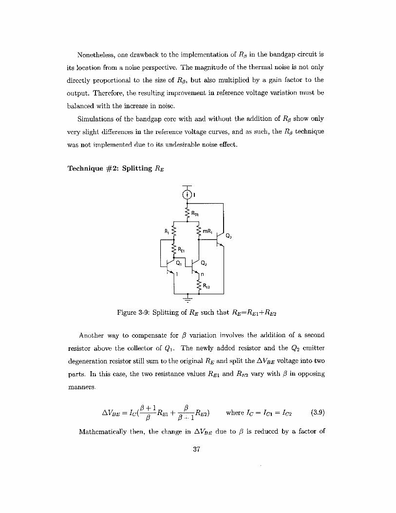
Technique #2: Splitting RE
RTR
R, mR,
REI
_, Q12
1 n
RE2
Figure 3-9: Splitting of RE such that RE=RE1+RE2
Another way to compensate for 3 variation involves the addition of a second
resistor above the collector of Q1. The newly added resistor and the Q2 emitter
degeneration resistor still sum to the original RE and split the AVBE voltage into two
parts. In this case, the two resistance values RE1 and RE2 vary with # in opposing
manners.
VBE=IC( RE1 + RE2) where Ic = Ici = C2 (3.9)aly t t+1 = isb
Mathematically then, the change in AVBE due to 3 is reduced by a factor of
37

# if RE1=RE2 from .±1 t3(,+1). However, as with Rp, the noise effect must be
considered as well as part of a holistic evaluation of the addition of RE1. Through
Vin
RR
Vout Vin + OVout+ I
vn r. } M g ro
(a) Test Circuit (b) Small Signal Model
Figure 3-10: Gain Analysis
analysis of the small signal model of Figure 3-10(b), the gain '"'(") is found to bevi"(5)
Vot r. (I - gmR) (3.10)Vin R + r.
From the equation above, zero gain can be achieved if gmR = 1 which occurs
when the voltage drop across the resistor R equals the thermal voltage k. Selectingq
the value of RE1 then based on the bias collector current through Q, could allow for
some # compensation while minimizing the resulting undesirable noise effect. One
important aspect to note is that the desired AVBE generated must be at least as large
as the thermal voltage in order to use this technique. Nevertheless, algebraic analysis
reveals that for unequal values of RE1 and RE2, the variation due to 6 is actually
worse than the original . difference, limiting the utility of the technique.
3.2.2 Emitter Area Ratio
One important degree of freedom embedded in the design of the bandgap core is
the emitter area ratio between Qi and Q2 that determines the magnitude of the
generated AVBE. While the chosen area ratio will impact the necessary layout area
of the bandgap core, its effect on the current density of Q2 is even more critical as
the larger the ratio, the smaller the current density.
38

From the low P discussion in the previous section, the magnitude of the space
charge region recombination current becomes increasingly important as the opera-
tional collector current decreases. Although both the hole injection and recombina-
tion current densities are generally scaled by just the emitter area AE to produce
the corresponding currents, the recombination current at the sidewall regions of the
base-emitter junctions cannot be ignored at low bias currents [9]. The inclusion of
sidewall recombination results in an increase in the effective recombination scaling
area, further decreasing the low current 3.
Aeff = BL + rXjeb(B + L) (3.11)1
/3 scaling factor = B+L (3.12)1 +7rje X L
A'f'
Figure 3-11: 3-D Representation of Base-Emitter Junction [9]
This analysis indicates then that the larger the area ratio, the greater the effect
of the recombination current on /. For the final bandgap design here, an area ratio
of four was chosen.
3.2.3 Collector-Substrate Leakage at High Temperatures
With the substrate connected to the lowest voltage and the bipolar device operating in
the forward active region, the only current flowing through the substrate should be the
leakage current from the reverse biased collector-substrate junction diode. At room
39

temperature, this current is normally negligible; however, as temperature increases,
the leakage current likewise increases rapidly with the following proportionality [11].
ileakage oc oc T3e (3.13)
120
100
U 8 0
60
40 -
20
0-50 0 50 100 150
Temperature (*C
Figure 3-12: Temperature Dependence of Collector-Substrate Leakage
Not only does the leakage current exhibit a strong temperature dependence, but
it is also proportional to the collector n-well size of the bipolar device. Although
the collector n-well size does not always scale with the emitter area of the bipolar
device depending on the fabrication process, devices with larger emitter area AE
generally have larger collector n-well sizes. As a result, the leakage current of the two
devices generating AVBE will be unequal at high temperatures. To compensate for
this difference, the extra leakage current can be taken away at the collector of Q, via
a dummy device that mimics the area size of Q2. Another method returns the extra
leakage current to the collector of Q2 through a current mirror in conjunction with
a dummy device. In both methods seen in Figure 3-13, the dummy device works to
maintain equal collector currents across temperature to keep the reference voltage as
stable as possible. When simulating the circuit that includes the equalizing dummy
device, the emitter area of the device is labeled as n-1 in order to simulate the collector
n-well size correctly.
40

,f I
fRTR
R1 mR1 Q3
Q, Q2
n-1 I n
RE
I I L
TR3
R mR1 3
1 Q
R2R
(a) Dummy Circuit #1 (b) Dummy Circuit #2
Figure 3-13: Equalizing Collector-Substrate Current Leakage
3.2.4 Layout and Matching Techniques
While some of the design options presented here can be used to compensate for process
variations, all of the previous mathematical analysis of the bandgap reference circuit
assumes that all devices of the same type are identical, when in fact this can never
be true. The mismatch between devices can be mitigated by employing good layout
techniques.
For instance, when placing bipolar devices for the core, the common centroid
technique is generally used, in which the devices comprising the transistor with the
larger emitter area are centered around the smaller device. Similarly, MOSFET
devices utilize common centroid layout while also employing interdigitization arrays
for best matching [12].
Well-matched resistors also play a large role in the accuracy of the simplified
reference voltage equations in Section 3.1.1. When matching different resistor values,
resistors of the same width are laid out, often in arrays of unit cells to ensure that
any value inaccuracies are consistent across all resistors being matched. In addition,
resistors with larger widths tend to match better than those with smaller widths to
a point.
41
n-1
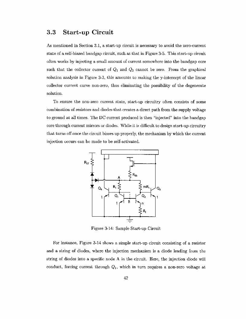
3.3 Start-up Circuit
As mentioned in Section 3.1, a start-up circuit is necessary to avoid the zero-current
state of a self-biased bandgap circuit, such as that in Figure 3-5. This start-up circuit
often works by injecting a small amount of current somewhere into the bandgap core
such that the collector current of Qi and Q2 cannot be zero. From the graphical
solution analysis in Figure 3-3, this amounts to making the y-intercept of the linear
collector current curve non-zero, thus eliminating the possibility of the degenerate
solution.
To ensure the non-zero current state, start-up circuitry often consists of some
combination of resistors and diodes that creates a direct path from the supply voltage
to ground at all times. The DC current produced is then "injected" into the bandgap
core through current mirrors or diodes. While it is difficult to design start-up circuitry
that turns off once the circuit biases up properly, the mechanism by which the current
injection occurs can be made to be self-activated.
1 B
RE
Figure 3-14: Sample Start-up Circuit
For instance, Figure 3-14 shows a simple start-up circuit consisting of a resistor
and a string of diodes, where the injection mechanism is a diode leading from the
string of diodes into a specific node A in the circuit. Here, the injection diode will
conduct, forcing current through Q1, which in turn requires a non-zero voltage at
42

node B. Once the voltage at Node A rises high enough such that the voltage drop
across the diode is too small for appreciable current to flow, the injection diode turns
off.
With a goal of minimizing the total quiescent current, the bias current of the
start-up circuit would ideally be very small since it will burn DC current at all times.
However, even though the bandgap circuit may only require a small amount of current
to ensure a non-degenerate state, caution must be exercised when lowering the bias
current of the start-up circuit so as not to render the start-up circuit ineffective.
3.3.1 Supply Voltage Dependence
Another consideration to be made is the variability of the bias current in the start-
up leg across supply voltage: for example, the bias current for the start-up circuit
in Figure 3-14 above scales directly with the supply voltage based on the value of
RST. In this case, although the current levels in the rest of the bandgap hardly vary
with supply voltage, the total quiescent current of the bandgap circuit can increase
significantly simply due to the start-up leg.
Depletion Mode PMOS
1VSG
11S0
-S G D
PD
(a) Enhancement Mode PMOS (b) Depletion Mode PMOS Cross SectionCross Section
Figure 3-15: PMOS Cross Sections [13]
To mitigate the direct proportionality of the current to the supply voltage, a
depletion mode PMOS is added in series with the start-up resistor RsT as shown in
Figure 3-17. Unlike enhancement mode PMOS devices used in the rest of the circuitry
43

here, the depletion mode PMOS device is fabricated with additional p-type dopant
implants in the channel of the device, requiring a positive threshold voltage to turn
off the device, as seen in the I-V characteristics graphed in Figure 3-16.
3.0
2.5
Z 2.0 -
91.5-
01.0-
0.5
0.0-2 -1 0 1 2 3 4 5
Gate to Source Voltage (V)
Figure 3-16: I-V Characteristics of Depletion Mode PMOS
By employing the voltage drop across RST as its gate to source voltage, the PMOS
device acts as a self-controlled current source once the supply voltage reaches a certain
value. Below that value, as the supply voltage rises, the current through the resistor
increases, likewise increasing the VGS of the PMOS. The increasingly positive VGS
reduces the current carrying capability of the PMOS by depleting away the majority
carriers in the channel. Finally, the current in the start-up leg stops increasing when
the resistor current and resulting VGS drop satisfy the following set of equations.
Rs -
Mxto BG
Figure 3-17: Start-up Leg with Self-Regulating Depletion Mode PMOS CurrentSource
44

VGS = -IDRST (3.14)
-ID = -2G _T2 (3.15)
Solving the equation set or running a test simulation reveals the value of VGS to
which the PMOS self-regulates. The value of RST can then be calculated based on
the maximum allowable current in the start-up leg.
4.5
4.0
3.5
3.0
2.5
.52.0
1.0
0.5
0.00.0 1.0 2.0 3.0 4.0 5.0
Supply Voltage (V)
Figure 3-18: Start-up Leg Current as a function of Supply Voltage for RST = 320MQ
3.3.2 Final Design
For the final start-up circuit leg using the topology of Figure 3-17, keeping with the
maximum current of 5nA per leg results in a RST value of 320MO. As the supply
voltage increases past a diode drop, the current flow will generate a non-zero voltage
at the gate of the current mirror injection device Mx. Once this NMOS has been
turned on, a direct path from the supply to ground will be created in the bandgap
core, initiating the flow of current and thus avoiding the degenerate operational state
of the bandgap circuit. As soon as the injection point in the circuit rises above a VBE,
Mx will begin to turn off, with full shut off once the injection node reaches the gate
voltage of Mx, that is VBE ± VGS-
45

3.4 Trim Range and the ZTC Voltage
As discussed in Section 3.1, the PTAT voltage is generated by scaling AVBE with a
resistor ratio. While hand calculations reveal the exact resistor values necessary for a
ZTC reference voltage for a given bias current, they can vary due to process variation
and device mismatch for any given fabricated part. To compensate for this variation,
the resistor RTR in Figure 3-4 is broken up into a string of resistors that make up
the trim range of the bandgap circuit. The purpose of this trim range is to fine-tune
the reference voltage, and thus the temperature coefficient once the part has been
fabricated by leaving in or shorting out various resistors that make up RTR.
Vb, Od RTR1Vbl I R1R
Vb2*-1 R2
RT 4 Vb3*- R3
V Ru4-
RTs
Figure 3-19: Trim Resistors
Good design practice dictates that the trim range designed into the circuit should
be made larger than the minimum range determined through simulation across process
combinations to account for any device inaccuracies and unknown sources of error.
Once the desired trim range is known, the remaining degree of freedom is the number
of bits the trim range should contain, thereby setting the number of trim resistors
and the size of the least significant bit (LSB). The size of the LSB determines how
well the trim range compensates for process variation in order to produce a reference
voltage with a temperature coefficient as close to zero as possible. Put another way,
a smaller LSB size allows for greater granularity when dialing in the desired PTAT
voltage component.
46

For the final bandgap core, the minimum trim range necessary simulated out to be
just over 40mV. Conservatively doubling this variation brings the total voltage drop
in the trim range to about 100mV with 5 selectable bits chosen for an LSB step size
of 3.23mV. This doubling is done to account for device mismatch in process variation
and model inaccuracies as the bias currents are lowered away from the well-defined
SPICE model operating points.
3.5 Bandgap Ready and Undervoltage Lockout Sig-
nals
The speed with which the bandgap reference voltage reaches its final value is de-
pendent on a number of variables such as temperature and the input supply ramp
rate. Depending on how the circuitry downstream relies on the reference voltage,
a bandgap ready circuit can be useful to shut down downstream circuitry to avoid
incorrect operation while the bandgap is still powering up. Similarly, an undervoltage
lockout (UVLO) circuit can be employed to shut down circuitry if the supply voltage
is too low for proper operation.
3.5.1 Bandgap Ready Circuitry
The bandgap ready signal is generally created by comparing two different voltage
nodes: one that reaches its final value very quickly and one that reaches a similar
value more slowly. Two examples of bandgap ready circuit topologies are discussed
below.
Topology #1: Comparing Collector Voltages
One way to generate the bandgap ready signal is to compare the voltages at the
collectors of Q3 and Q4 in the bandgap core. Due to the diode connection of Q1, the
VBE of Qi and Q4 will quickly approach its final value at start-up. On the other hand,
while VBE1 also immediately fixes the voltage at the base of Q2, the degeneration of
47

RTRi 21
R, BGREADY
Q4 Q3
1 H10 1
RE
Figure 3-20: Bandgap Ready Comparator Topology #1
Q2 as well as the difference in emitter area results in the collector current of Q2
reaching its final value at a slower pace. In addition, any compensation capacitance
placed at the collector of Q3 to ensure AC stability will slow the rise of the collector
voltage due to the increased capacitance charging time. Thus, the bandgap ready
signal trips once the collector voltage of Q3 is close to that of Q4, indicating that the
bandgap circuit is close to its final DC operating point, as seen in the results of a DC
sweep simulation on the supply voltage in Figure 3-21.
2.00
1.75
1.50
1.25
1.00
-0.75-
0.50
0.25
0.001.00 1.25 1.50 1.75 2.00
supply V~eCw i t
Figure 3-21: Supply Voltage DC Sweep Simulation Results for Topology #1
48

RTR
BGREADY
Q4 R, R, Q3 Q
1Q5 2 RBGR
RE
Figure 3-22: Bandgap Ready Comparator Topology #2
Topology #2: Comparing Currents
Rather than using a differential pair, another method is to use a current mirror as
a form of current-difference comparison to generate the desired signal. Part of the
simplicity and variability of this topology is that the trip point is the point at which
the current in the two legs of the mirror balance perfectly. The diode connection
of the left half of the current mirror sets up quickly as the collector voltage of Q2
reaches its final value; on the right half of the current mirror, the output node rises
as current flows through the resistor as the current mirror works to reach its balance
point. Once the balance point is reached, the bandgap ready signal trips.
2.00
1.75
1.50
1.25
11.00
0.75-
0.50
0.25
1.00 15 1.50 1.75 2.00Supply Voltage (V)
Figure 3-23: Supply Voltage DC Sweep Simulation Results for Topology #2
49

3.5.2 UVLO Signal Circuitry
The utility of the UVLO signal comes in detecting whether or not the minimum
supply voltage specification has been met, which can be critical for proper operation
of certain blocks. Like the bandgap ready signal, the state of the UVLO signal is
determined through a comparison of two values: the supply voltage and some kind
of a reference term.
Topology #1: Using the Bandgap Reference
BGREADY -F>H
R
cR V UVLO
VREF +-
Figure 3-24: Bandgap Circuit Dependent UVLO Signal Circuit
One topology for producing the UVLO signal follows directly from the bandgap
circuit, whereby a pre-determined fraction of the supply voltage is compared to the
reference voltage produced in the bandgap circuit. In this case, the bandgap ready
signal would be used to keep the UVLO circuitry off until the desired comparison can
be made.
Topology #2: Bandgap-Inspired Circuitry
A different UVLO topology presented in Figure 3-25 is independent of the bandgap
circuit although still largely based in bandgap principles. Mimicking the core of a
different type of basic bandgap cell, the Brokaw cell, the circuit implements a current
difference comparison between the two legs based on the supply voltage dependent
bias applied to the bases of Q, and Q2. Since the combination of Q1, Q2, R 1, and R 2
is designed using single cell bandgap equations, the trip point of the current difference
50

comparator occurs when the voltage applied to the bases of the bipolars is equal to
the bandgap voltage.
R
1 0 1 Q2 UVLOcR
R2
R,
Figure 3-25: Bandgap Inspired UVLO Signal Circuit where 7VSUPPLYMIN VREF
When the supply voltage is too low, the collector current of Q2 wants to be greater
than that of Q1, pulling down the current mirror output node. Conversely, when the
supply voltage is greater than the minimum value, the opposite is true, pulling up
the current mirror output node and switching the state of the UVLO signal.
Similar to the start-up circuit, the resistor divider leg in the two above topologies
suffers from the same current scaling effects with the supply voltage, which can also
be alleviated through the implementation of the self-regulated current source with a
depletion mode PMOS device.
3.5.3 Combining the Bandgap Ready and UVLO Signals
As described in the last two sections, the bandgap ready and UVLO signals both serve
to avoid incorrect operation but switch state with different triggers. Comparing the
bandgap minimum supply voltage and the specified system minimum supply voltage
reveals that the two values differ by only 300mV. Thus, the overall quiescent current
in the system could be decreased if the two signals were combined into one as this
would allow for the elimination of one entire circuit block.
51

Bandgap Ready Signal Base
Knowing when the bandgap reference can be used reliably is critical to regulating
the output voltage to the desired level since it is used in the sleep comparator. This
section will explore the possibility of modifying the existing bandgap ready circuitry
to fit UVLO specifications.
Since the lower-bound supply voltage specification is higher than the minimum
supply voltage required for the bandgap circuit, the limiting case is when the supply
voltage comes up slowly. In this case, the bandgap ready signal could be triggered
before the supply voltage has reached the minimum specified system supply voltage.
Transient simulations with varying ramp rates for the supply voltage can be run to
determine the difference in the thresholds.
2.0
1.8
1.6
1.4
21.2
t 1.0
0.8
0.6
0.4
0.2 m0.0 , a
0.0 0.5 1.0 1.5 2.0
Supply Voltage M
-12M - - 24M - - -48M
Figure 3-26: Bandgap Ready Circuit Supply Voltage DC Sweep Simulation for VariousRBGR
Based on the data above, the minimum supply voltage at which the bandgap
ready signal triggers is in the range of approximately 1.1V to 1.3V depending on
the value used for the resistor RBGR in the current difference comparator. Since the
supply voltage at the trip point is about one forward diode drop below the minimum
supply voltage, the bandgap ready signal could also serve as the UVLO signal with
the addition of a forward diode drop somewhere in the comparison, such as in the
two topology variations introduced below.
52

Variation #1: Output Node
BGREADY
Va RBGR
Figure 3-27: Bandgap Ready Topology Variation #1
In the first variation, the diode drop recovery is attempted just above the output
node of the bandgap ready signal comparator. Here, the hope is that the rise of
the output node will be slowed by the additional voltage drop incurred by the diode
connected device. Nonetheless, based on the simulation results, the additional diode
drop in the output leg does little to affect the supply voltage at which the bandgap
ready signal trips.
2.00
1.75
1.50
1.25
1.00
0.50
0.25
1.00 1.25 1.50 1.75 2.00
Figure 3-28: Bandgap Ready Topology Variation #1 Supply Voltage DC Sweep Sim-ulation
53

BGREADY
VQ RBGR
Figure 3-29: Bandgap Ready Topology Variation #2
Variation #2: Supply Voltage
When the diode drop is instead placed in series with the supply voltage, it lowers
the effective supply voltage seen by the comparator. In this case, the addition of the
diode connected device does increase the supply voltage at which the bandgap ready
signal trips by slowing the rise of all nodes in the bandgap circuit. However, the
variability in the diode drop of the MOS device across process makes the technique
rather inexact.
2.00
1.75
1.50
1.25
41.00
0.75
0.50
0.25
0.001.00 1.25 1.50 1.75 2.00
Supply Voltage (V)
Figure 3-30: Bandgap Ready Topology Variation #2 Supply Voltage DC Sweep Sim-ulation
54
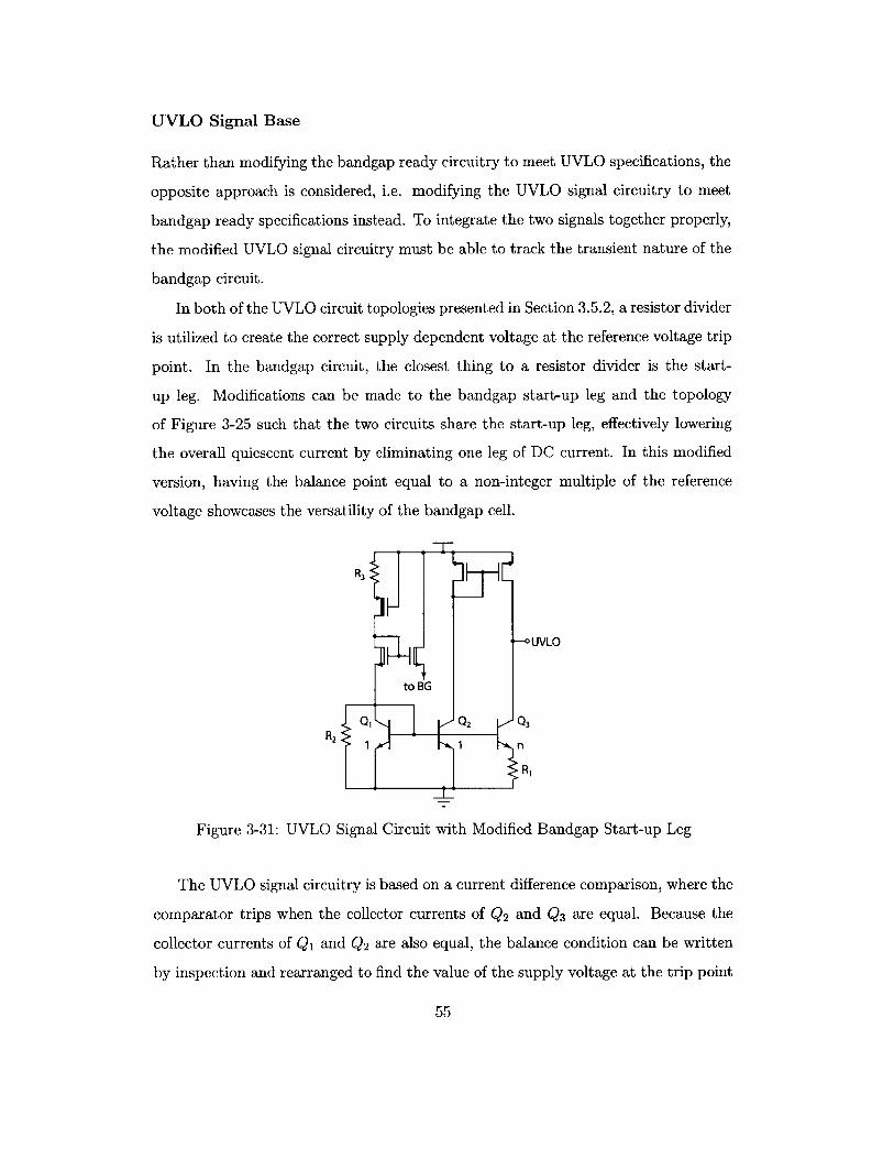
UVLO Signal Base
Rather than modifying the bandgap ready circuitry to meet UVLO specifications, the
opposite approach is considered, i.e. modifying the UVLO signal circuitry to meet
bandgap ready specifications instead. To integrate the two signals together properly,
the modified UVLO signal circuitry must be able to track the transient nature of the
bandgap circuit.
In both of the UVLO circuit topologies presented in Section 3.5.2, a resistor divider
is utilized to create the correct supply dependent voltage at the reference voltage trip
point. In the bandgap circuit, the closest thing to a resistor divider is the start-
up leg. Modifications can be made to the bandgap start-up leg and the topology
of Figure 3-25 such that the two circuits share the start-up leg, effectively lowering
the overall quiescent current by eliminating one leg of DC current. In this modified
version, having the balance point equal to a non-integer multiple of the reference
voltage showcases the versatility of the bandgap cell.
~T_
R3
-- 0UVLO
to BG
F, Q2 Q3
R2 1 n
R1
Figure 3-31: UVLO Signal Circuit with Modified Bandgap Start-up Leg
The UVLO signal circuitry is based on a current difference comparison, where the
comparator trips when the collector currents of Q2 and Q3 are equal. Because the
collector currents of Q, and Q2 are also equal, the balance condition can be written
by inspection and rearranged to find the value of the supply voltage at the trip point
55

as follows.
VSUPPLY - VBE - VGS VBE 1 kI______-_- -__=_- --- in n (3.16)
R3 R2 R1 qR3 R3 kT
VSUPPLY = (1 + )VBE VGS + - In n (3.17)R2 R1 q
Both the VGS and VBE of MOS and bipolar devices respectively have negative
temperature coefficients, so the same bandgap principles can be applied to the sizing
of the resistors such that the supply voltage trip point is independent of temperature.
However, when determining the amount of PTAT compensation necessary, the VGS
of the MOS device must be weighted by 1.5 so as to take into account the difference
in the negative temperature coefficients as shown in Figure 3-32.
0.8
0.7
0.6
0.5 slope = -2.4mV/*C
20.4
.-- slope =-1.5mV/*C
0.2 -
0.1 -
0.0-50 0 50 100 150
Temperature (*C)
- - VGS -VBE
Figure 3-32: VGS and VBE Temperature Coefficients for 5nA of Drain and CollectorBias Currents
3.5.4 Final Design Integration
Since the UVLO signal circuitry was found to be more amenable to modifications to
meet bandgap ready conditions, the bandgap ready signal circuitry was eliminated
from the final bandgap design. In implementing the UVLO signal circuitry, its mini-
mum temperature stable supply voltage trip point can be calculated from the known
56

npn VBE and NMOS VGS at the current trip point.
VSUPPLY =VBE + 1.5VGSVBE
Unfortunately, at the desired current trip point of 5nA, the calculated minimum
supply voltage is about 1.9V, which is slightly higher than the specified minimum
system supply voltage. The necessary elimination of the diode connected NMOS
from the start-up leg in order to achieve the desired supply voltage trip point thus
requires separating the UVLO signal circuitry from the bandgap circuitry. Although
this separation means that the additional leg of DC current must be added back
into the circuit, the combined consumed current of the bandgap and UVLO blocks
together still just meets the target current goal of 50nA.
RST
-> -UVLO
Q1 Q2 Q3R2
R,
Figure 3-33: UVLO Signal Circuit
As the core of the UVLO block is very similar to the bandgap circuit, a similar
design procedure can be used to determine the parameter values for the UVLO cir-
cuitry. First, the balance condition of Eq 3-16 is re-written to reflect the elimination
of the diode-connected NMOS in the start-up leg.
VSUPPLY - VBE VBE 1 kTRST R2 R 1 q
57

RST RST kTVSUPPLY = (1 + RS-)VBE + In n (3.20)
R2 R 1 q
In continued imitation of the bandgap circuit, the emitter area ratio in the UVLO
circuit was selected to be four with the current trip point set at 5nA, making the
value of the degeneration resistor R1 of Q2 equal to 7.2MQ as well. Calculating the
necessary PTAT voltage using the specified minimum supply voltage then determines
the values of the the remaining resistors.
VSUPPLYVPTAT = VSUPPLY - VREF VBEI I=5nA (3.21)
VREF
RST = R1 VTnn= 189.6MQ (3.22)- In nq
R2 = RST 433.2Mg (3.23)VREF
Simulating the UVLO block across temperature and process corners with the re-
sistor values calculated above revealed that the UVLO signal did not switch states for
certain process corner and temperature combinations since the npn collector currents
never reached the trip point of 5nA. To restore the intended UVLO block function-
ality, the start-up resistor RST was split into two separate resistances to ease the
current limiting effects of the depletion mode PMOS. One of the two resistors contin-
ued to set the VGS of the depletion mode PMOS, and the other resistor was used to
connect the drain of the depletion mode PMOS to the collector of Qi. To minimize
the resulting increase in current consumption, simulations sweeping the value of the
start-up resistor bounded by the depletion mode PMOS were run to determine the
minimum split needed to restore proper operation.
To be able to fully use the UVLO signal as a replacement for the bandgap ready
signal, the UVLO comparator must trip after the reference voltage is close to its
final pre-trim value. To ensure this condition, the UVLO and bandgap blocks were
simulated together at a specified supply voltage, and the reference voltage and UVLO
signal curves plotted together. From the simulations, the UVLO signal appeared to
58

switch states before the reference voltage had reached within 1OOmV of its final value
for certain process corners. To slow down the UVLO signal block to match the
transient nature of the bandgap block, a load capacitor was added to the output of
the current difference comparator. To keep the additional layout area needed as low
as possible, simulations sweeping the load capacitance value were run to determine
the minimum load capacitance needed, which was 5pF.
3.6 Proof of Concept
As presented in Section 2.3, thirteen different quiescent current level versions of the
LTC3588 were fabricated to explore the effects of lower current levels on chip opera-
tion particularly in the bandgap and sleep comparator blocks. The bandgap circuit
was evaluated over temperature for each of the five different bandgap current levels,
ranging from the original 250nA down to 50nA. The operation of the bandgap cir-
cuit with the lowest current level is valid proof of concept for the bandgap design
presented in the next section because the current per leg of the two circuits is very
similar (6.67nA/leg fabricated to 5nA/leg designed), and the total quiescent current
level is the same for both.
3.6.1 Measurement Setup
To evaluate the chips, a part was placed on an evaluation boad with posts for each
pin connection. Since the objective specifications laid out in Table 1-1 are based on
operation during the sleep state, the output node was connected to the supply voltage
externally to keep the converter off at all times. An adjustable power supply was
connected to the input supply voltage pin, and Agilent multimeters and a Keithley
picoammeter were used to monitor the supply and reference voltages and current
levels.
59

Figure 3-34: Evaluation Board
Across the supply voltage range of 1.8V to 5V, room temperature measurements
of the total supply current, the bandgap block current, the reference voltage, and
the supply and reference voltages at the bandgap ready signal trip point were taken.
Reference voltage measurements were then taken for a supply voltage of 3.5V across
the temperature range of -50 C to 130*C in 20 C increments.
3.6.2 Measurement Data and Analysis
Temperature Variability
1.205 -
1.195 1
51.185 -
.1.175 -
1.145
1.135 -1.125 -
- -- -
-50 -30 -10 10 30 50 70 90 110 130 150Temperature (*C)
-EXPOl - - EXPO2 - - -EXP03 - -EXPO4 - -EXPOS
Figure 3-35: Measured Untrimmed Reference Voltage with VSUPPLY=3.5V
The untrimmed reference voltage data shown in Figure 3-35 displays a wide spread
60

of over 50mV at room temperature across the different current levels, while also ex-
hibiting a greater negative temperature coefficient for lower current levels. However
the increasingly negative temperature coefficient can be explained by revisiting the
reference voltage equation. The original LTC3588 bandgap circuit was designed for
operation at 40nA/leg, which fixes the VBE component of the reference voltage equa-
tion at a particular value. Therefore, the amount of PTAT voltage designed into that
particular bandgap circuit is the ideal reference voltage of 1.2V minus the VBE needed
by the npn at 40nA of collector current at room temperature. Any npn bipolar then
running at a collector current less than 40nA would exhibit a lower VBE, requiring a
larger PTAT voltage to be added to it to sum to the ideal reference voltage.
1.205 -
1.195 -
~1.185
... . .
-1.175 -
S1. 165
1.155 -
1.145 -
1.135
1.125-50 -30 -10 10 30 50 70 90 110 130 150
Temperature (*C)
-EXPO1 - - EXP02 - --EXPQ3 - -EXPO4 - -EXP05
Figure 3-36: Measured Trimmed Reference Voltage with VSUPPLY=3.5V
After parts of each type were trimmed, not only did the magnitude of the tem-
perature coefficients of the reference voltage drop dramatically as expected, but the
spread in reference voltage across the different current levels also decreased signifi-
cantly as seen in Figure 3-36. However, the flattest reference voltage could not be
reached for some of the lower current levels because the calculated number of bits to
trim was between two different combinations or greater than the maximum number
of possible trim bits.
To construct the theoretical flattest reference voltage curve for each part graphed
61

in Figure 3-37, the actual LSB size at each temperature point was calculated based
on the pre-trim and post-trim reference voltage data and then combined with the
pre-trim reference voltage data to simulate trimming a non-integer number of bits.
1.205 -
1.195 -
1.185 - - -- -- - -- ----- --
to1.175 -
C1.165 -
! 1.155 -
1.145 -
1.135 -
1.125-50 -30 -10 10 30 50 70 90 110 130 150
Temperature (*C)
-EXPO1 -- EXP02 -.- EXP03 -- EXPO4 -- EXP05
Figure 3-37: Simulated Reference Voltage
LSB size VREFUT - VREFT (3.24)# of bits trimmed
Although the reference voltage curves constructed with the ideal trimming are
very similar to the measured post-trimmed part data, the constructed curves further
demonstrate the potential of low current bandgap circuits to produce stable reference
voltages across temperature if the PTAT component is adjusted properly.
Supply Voltage Variation
Aside from temperature, another variable that could affect the bandgap circuit op-
eration is the supply voltage. To check for supply voltage dependence, measured
reference voltage data was taken at room temperature (T=22 C) through the speci-
fied supply voltage range of 1.8V to 5V in 1OOmV increments. As seen in Figure 3-38,
the reference voltage is does not vary across supply voltage.
62

1.21
1.20
51.19
bo1.18
. 51.17ba
C
ca 1.16
1.15
1.14
2.5 3.0 3.5 4.0 4.5Supply Voltage (V)
-EXP01 - - EXPO2 - - -EXP03 - -EXPO4 - -EXPOS
Figure 3-38: Untrimmed Reference Voltage with Varying
5.0
Supply Voltage
3.7 Final Design
3.7.1 Schematics
RSTM4 M5 M,,l5/320 5/320 4/40
320MO2 2
M, M M6 M1220/5 5/8 5/8 4/40
2 2
M134/2
M2 M3
M,42
10/8 10/1 100/0.8 1
1 4 VREF
3pF
Q/ 9 VTR RT M1,10/0.8 1VTR s
1 4 R, R2 8
Q3 120MO 120Mf Q4
C, 1 Q, Q2 2
3pFr 9 4
R37.2MO)
Figure 3-39: Bandgap Circuit
63
M144/40
Mis4/40
M164/2
M170.10/0.8
Q5
2
-. . . . . .. . . . . . .. . ..-.. . . . . .

VREF
M, XM2
Vb4 1.4/0.6 RT45.16Mn
M, X2 M4Vb3 1.4/0.6 R6
2.58MO
M5 X3 M,
R 4 - Vb2
1.4/0.6
(from M" X aFig 3-39) V645k
M, X, MIOVbO 1.4/0.6 Rro
322.5kn
Figure 3-40: Bandgap Trim Network
M3 Ms
RaS 4/256 4/256160MO 2 2 M8
M, 1.4/6
4/12.8 4/12.8
2 2 M,1/0.6
29.6MO7
M,01/0.6
R2 Q, Q2 Q3I
43.2E 5p Ml-4M
43.M1 1 '4 1./6
1/0.6 84MD 7.2MD
-UVLO
Figure 3-41: UVLO Signal Circuit
3.7.2 Simulation Results
As can be seen in the bandgap simulation data over temperature in Figure 3-42, the
bandgap reference voltage is nearly constant across temperature as expected at about
1.18V. For the UVLO circuit, M2 and R3 (in Figure 3-41) create a DC hysteresis of
approximately 40mV in the supply votlage UVLO trip threshold. For the two blocks
64

IBG,SUPPLY 30nAVREF (T=25 C) 1.1769V
AVREF across T= [-50 0C,130 'C] 3.3mVIUVLO,SUPPLY 21.5nA
VSUPPLY (UVLO Rising Threshold) 1.749VVSUPPLY (UVLO Falling Threshold) 1.712V
Table 3.1: Key Bandgap and UVLO Simulation Data
combined, the total supply current is 51.5nA, as
above the total allocated current of 50nA.
1.25 -
1.24 -
1.23
1.22-
1.21 -
1.20
1 1.19 -
1.17 -
1.16 -
1.15-50 -30 -10 10 30 50 70
Temperar (C)
Figure 3-42: Simulated Bandgap Reference Voltage5V
listed in Table 3-1, which is just
90 110 130
over Temperature at VSUPPLY =
2.0
1.6
51.2-
0.8-
0.4
0.0
*
0.0 0.5 1.0 1.5 2.0 2.5
Supply Vo1ta. (V)
Figure 3-43: Simulated UVLO Signal over Supply Voltage
65

66

Chapter 4
Sleep Comparator
In order to determine whether or not the buck converter should be on, the system em-
ploys a comparator that continuously checks a pre-determined fraction of the output
voltage against the bandgap reference. If the output voltage drops below the desired
value, the comparator outputs a digital low signal that turns on the buck converter.
Conversely, if the comparator senses that the output voltage is back in regulation, its
output is a digital high signal that turns off the converter.
4.1 Design Considerations
Ideally, the comparator will trip near instantaneously such that the output voltage
remains as close as possible to the desired value. However, finite propagation delay
in the comparator creates higher voltage ripple at the output node than the DC
trip points would suggest because the output will continue to slew during the delay.
While the amount the output slews is dependent on the size of the output capacitor,
a smaller delay time results in a lower minimum output capacitor needed to achieve
a specified output voltage ripple.
For a very small propagation delay, each stage of the comparator should have a
large slew rate at its output while achieving high gain. Both characteristics can be
reached with a high bias current and large device transconductance. However, the
attainable bias current in the comparator is constrained by the target 50nA quiescent
67

current for the whole block as defined in Chapter 2. As such, the difficulty lies in
how to best minimize the delay time given a total available quiescent current. For
comparison purposes, the target maximum allowable propagation delay is the delay
time achieved by the sleep comparator in the LTC3588 running at the same total
quiescent current level.
4.2 BJT and MOS Device Characteristics
4.2.1 MOS in Subthreshold
MOS devices are generally operated in the triode or saturation regimes, in which
excess carriers in the inversion layer move from the drain to source via drift. However,
when the gate-to-source voltage VGS is less than VT, the device is not off entirely but
rather still conducting a small amount of current. This is known as the weak inversion
or subthreshold regime, wherein the free carriers in the space charge region move by
diffusion similar to in a bipolar device.
Like the bipolar, the current through a MOS device in subthreshold is exponen-
tially proportional to the gate to source voltage [10].
qVG15 W qVZID = oe nkT (1 + AVDS) where I, = WpCthe-nkT and n>1 (4.1)
L
The expression for the transconductance of a MOS device in subthreshold is then
found to be that of the bipolar expression multiplied by an additional - factor. The
intrinsic gain expression gmr0 for the two device types can then be written as follows.
MOSFET: g.ro = -ID _ _ _ ___2nkT IDA kT n(
BJT: gro = V = - VA (4.3)kT Ic kT
With typical values for VA of at least 30V and A of at around 0.1V 1 , the gain
of bipolar devices will typically be higher than that of MOS devices operating at the
68

same bias current.
4.2.2 Differential Pairs
Since MOS devices in subthreshold behave similarly to BJTs in addition to maximiz-
ing their transconductances per unit of bias current, MOS and bipolar devices can
be considered analytically interchangeable for the input devices of each differential
stage of the comparator. Thus, the other differing characteristics between the two
influence the type of device selected in each stage.
Input Current
Minimization of input current into the first stage of the sleep comparator is critical
in order to maintain an accurate reading of the output voltage because the input
current is stolen from the feedback resistor divider at the output, creating an error
in the output divider. Using MOS devices as the input pair of the sleep comparator
offers the benefit of zero input current due to infinite gate resistance whereas bipolar
devices require a small amount of input current into the base node for operation. To
mitigate the effects of the non-zero base current, the values of the resistors in the
output feedback divider can be reduced so that any input current taken away is a
smaller fraction of the total current through the divider. However, this technique
increases the total current consumption of the divider.
Another technique for diminishing input current in the bipolar case is base current
cancellation. The premise of this approach is to inject the necessary base current into
the two base nodes of the input pair from elsewhere, thus eliminating the need for
either the reference or feedback node to provide the base current. With this technique,
even if the exact amount of base current is not fully injected, the amount of current
taken from either input node is still greatly decreased, increasing the effective # of
the input bipolars as seen by either input node. Therefore, the effect of any mismatch
between the / of the input bipolars is likewise reduced due to the boosted effective
03.
69

8 1B R R 1B
REF FB
1 ~214
Figure 4-1: Base Current Cancellation Technique
Input Offset
For any differential pair, its input offset voltage influences the accuracy of its input
voltage trip point. When the pairs are cascaded in multiple stages, only the minimiza-
tion of the input offset of the first stage is key as the input offset of the subsequent
stages referred back to the input will be divided down by their respective cumulative
gains.
For typically well-matched npn's, the input offset at 3o is of the order of 1-2mV.
On the other hand, for MOS devices, the 3a input offset is approximately 3mV. ForVWLa smaller offset, the input MOS devices must be large, generally with a very large W
compared to L. However, the larger the MOS device, the slower it is due to increased
parasitic capacitances, which increase the loading on the preceding stage and result
in a slower slew rate as will be discussed below. For both device types, the variation
of the input offset in the differential pair over temperature is not well characterized.
Capacitive Loading
An indication of the speed of the response of the stage to differential changes at the
input, the slew rate at the output node of the stage is effectively the charge rate of
70

the parasitic capacitances by the bias currents. For the system here, the bias current
of the stage is limited by the total block target quiescent current.
For the bipolar device, the dominant parasitic capacitances are those from the
base-to-emitter, base-to-collector, and collector-to-substrate. In the forward active
regime, while all three junctions will possess a component corresponding to their
respective pn junction depletion capacitances, the base-to-emitter junction will see
an additional diffusion capacitance CB in parallel with its depletion capacitance Ce.
The depletion capacitances of the three pn junctions decrease from their zero-bias
values with a 1 factor, where VD is the applied bias and Ob is the built-in
potential of the associated pn junction. A function of the bias current, the diffusion
capacitance CB is the product of the transconductance g, and the forward transit
delay F.
Coer Emtter Ban Base Emitter Collector
1Wo P Epi n IOP Epi nIS
BL n+BL+
Figure 4-2: Bipolar Device Cross Section [14]
npn pnp
Cie 15.3 fF 5.5 fFCjc 16.7 fF 6.5 fFCjs 35.6 fF 103 fF
Table 4.1: npn and pnp Junction Capacitances at Zero Bias
In the MOSFET device, the parasitic capacitances are those from the gate-to-
source Cg, gate-to-drain Cgd, source-to-body Cb, and drain-to-body Cdb. Included
in both the gate-to-source and gate-to-drain capacitances are components resulting
from the channel charge and the gate overlap with the source and drain diffusion
wells. The source-to-body and drain-to-body capacitances are made up of the vertical
depletion junction capacitance and the sidewall capacitance of the source and drain
diffusion wells created by the pn junction from the source or drain to the body.
71

GJAe G&WeBody Source rain Body SoreDrain
bso P PwllP o P Nw&l nIS2 . Bpi a Epi n
BL n+ BL n+
Figure 4-3: MOS Device Cross Section[14]
NMOS PMOSCo 2.4" 2.4mCj 0.52m-' 0. 72 "n
Ci,, 0.34 0.30
Cgdo 0.19 0.25 n
Table 4.2: NMOS and PMOS Parasitic Capacitances at Zero Bias
From the process data in Tables 4-1 and 4-2, the parasitic capacitances of a
minimum-sized MOSFET are much smaller than those of the bipolar, which would
favor using MOSFETs as the differential pair input devices. However, if the MOS-
FETs are sized such that their input offset is comparable to the bipolar input offset,
the MOSFET parasitic capacitances become much larger than those of the bipolar.
The larger load capacitances indicate that the speed of the stage will be slower as
the larger capacitances take longer to charge and discharge while also decreasing the
bandwidth of the stage by lowering the frequency of the pole at the output node.
The main tradeoff between using MOSFETs or bipolars then is between having
increased input offset or a non-zero input current.
4.3 Hysteresis
To avoid false tripping or chatter at the comparator output due to noise or other
disturbances, AC and/or DC hysteresis is often incorporated into the comparator
itself. If the comparison being made is clocked rather than continuous, a latch can
be used to ensure that the output changes only at the correct time.
72

DC Hysteresis 21 1
1 Schmitt Trigger
!AC Hysteresis
vI F ) s- v OUT
Figure 4-4: Two Stage Comparator with AC and DC Hysteresis Circuitry
4.3.1 DC Hysteresis
When implementing DC hysteresis, the rising and falling trip points of the comparator
differ and are symmetric with respect to the desired trip point: the rising trip point is
higher than the desired value, and the falling trip point is lower than the desired value.
With this method, chattering due to noise can be mitigated since the differing trip
points work like positive feedback thereby reinforcing the transition in both directions.
To generate the DC hysteresis, resistors can be placed in series with the input
devices, with the resistors on the two sides alternately shorted out based on the
comparator output, as marked on the left side of Figure 4-4. Moreover, the series re-
sistance slows down the comparator, and using MOS devices to short out the resistors
can cause false tripping.
However, since the current in the output inductor cannot change instantaneously,
some inertial hysteresis exists as well, which can eliminate the need for explicit DC
hysteresis. Rather than directly changing the comparator trip points, the time it
takes for the current acting on the load to change directions can be considered "dead
time" during which the comparator decision is reinforced.
Unlike explicit DC hysteresis, the amount of inertial hysteresis in the comparator
is not precisely defined, due to its dependence on the size of the inductor as well as
the output voltage being generated and the load. These parameters define how long
73

it takes for the output voltage to stop changing. Furthermore, the deviation at the
output from the desired value at the end of this time period is contingent upon either
the average charging current or the load current in addition to the size of the output
capacitor.
Aside from generating hysteresis at the comparator inputs, a Schmitt trigger can
be utilized at the output as well to further protect the system against noise, such as
at the output in Figure 4-4. In this case, the Schmitt trigger operates as an inverter
with varying rising and falling thresholds created using positive feedback with greater
than unity gain. Similar to the input hysteresis, the Schmitt trigger works to ensure
that the comparator transition is reinforced.
4.3.2 AC Hysteresis
Chatter at the comparator output feeding into the Schmitt trigger can be avoided
by employing AC hysteresis at the comparator output node using one shot circuitry.
The one shot circuitry not only increases the slew rate of the output stage of the
comparator right at the transition point of the inverter at the output, but also works
to reinforce the comparator decision at the trip point by holding the output node of
the last stage in the desired state during the transition. The AC hysteresis can be
accomplished using logic gates and a RC delay to set how long the output node is
held at the transition point as seen in the center marked subcircuit of Figure 4-4.
4.4 Adaptive Biasing
With the objective of lowering the quiescent current consumed while the buck con-
verter is sleeping without compromising speed, one solution is to simply lower the
operating current of the comparator during the sleep state, while providing extra
bias current during the active state.
Increasing the bias current during the active state can create switching noise due
to turning on and off the devices that provide the extra current as well as change
the gain of the associated stage(s) of the comparator. Caution must be exercised
74

21I 2I I2 1 1
OUT
Figure 4-5: Two Stage Comparator with Adaptive Biasing
so that the bias current increase or decrease does not cause false tripping during
the transition. Another option that fulfills the same goal is to have two different
comparators, one optimized for the sleep state at the target current level and one
optimized for the active state at a higher current level.
4.5 Gain per Stage
When designing the comparator, another consideration is the number of stages. In
considering current consumption, fewer stages means fewer legs of current, allowing
each stage to have a higher proportion of the total block quiescent current. Based on
the device behavior described above, the increase in bias current should decrease the
propagation delay of the stage due to to a larger slew rate at the output node. At
the same time, for a given overall gain, the gain per stage must be higher for fewer
stages.
From this qualitative analysis, increasing the total number of stages initially can
decrease the propagation delay. For a given total current level, the propagation delay
will begin to increase once the benefits of lower single stage gain are over-shadowed
by the delay from lower bias currents.
In distributing the gain and bias current in a multistage comparator, the propaga-
tion delay of the first stage proves to be the dominant factor in the total propagation
75

delay. The disparity in the delay of the first stage to that of the other stages is the
result of the size and rate of change of the differential input being detected. To min-
imize the disparity, the first stage carries more bias current than any other stage in
the comparator.
4.6 Topology Comparison
In designing the new sleep comparator, many different topologies were simulated to
capture the benefits of both MOS and bipolar devices. Topologies that were under
consideration but not listed below were eliminated due to headroom constraints at
the minimum supply voltage.
4.6.1 Topology I
91 4.51
Re, R,
SLEEPVREF
"VFB
R2 R2 R2
Figure 4-6: Topology I
In the LTC3588, a two stage topology couples an input MOS differential pair with
explicit DC hysteresis to a common source output stage for a wide output swing and
additional gain. In this topology, not only are MOS devices used as the input devices
to eliminate input current, but they are also near minimum sized for the best speed
performance. To alleviate inaccuracies due to mismatch in the MOS devices, source
degeneration is implemented in the current mirror of the first stage even though
76

doing so decreases the gain of the stage. A one-shot circuit is also employed to reduce
possible chatter at the output.
Since this project is based on the LTC3588, the performance of the following
different comparator topologies are compared against that of the original LTC3588
comparator with and without explicit DC hysteresis running at the same target qui-
escent current in the sleep state.
4.6.2 Topology II
21 21
SLEEP
VREF HVFB
Figure 4-7: Topology II
For Topology II, the inputs feed into a PMOS-based source follower (SF) stage
that is followed by an npn-based differential pair stage and a common source amplifier
output stage. Although the SF stage increases the number of total stages and con-
sumes current, its buffering action for the reference and feedback nodes are not the
limiting factor in decreasing the total propagation delay due to its unity gain. An npn
differential pair is used for the comparison computation rather than MOS devices to
minimize both the input offset and self-capacitive loading while maximizing intrinsic
gain.
Since the single-ended output of the differential pair is taken such that the output
stage is at zero bias in the sleep state, the bias current can be distributed between
the SF and npn differential stages. Based on the delay time contribution of each
77

stage determined through simulation, most of the current is allocated towards the
npn differential stage to maximize comparator speed.
Due to the headroom constraints imposed by the 1.8V minimum input supply
voltage, the reference input voltage selected for this topology is 0.6V rather than 1.2V.
The decrease in the common mode voltage ensures that the PMOS input devices in
the SF stages have enough overdrive in the balance state.
4.6.3 Topology III
~T~
, 41, 41, 1,
SLEEP
VREF VFB
r ei2.51, 141,
Figure 4-8: Topology III where I1 = I
Similar to the previous topology, the inputs again are initially buffered by a
PMOS-based SF stage that requires a 0.6V common mode input voltage and sub-
sequently feeds into an npn differential pair. In this topology, the common source
output stage is replaced by a folded cascode made of MOS devices attached to the
outputs of the differential pair. The comparator output is then taken directly off of
the output of the folded cascode.
Again, most of the bias current is allocated towards the combined npn differential
pair and folded cascode stage. In splitting the bias current between the two parts,
the most important aspect is that the current through the NMOS cascode devices
never falls to zero due to the increased delay time resulting from the reformation of
the inversion layer and charging of the parasitic device capacitances.
78

4.6.4 Topology IV
1 3 3
VREF 4/r VFB SLEEP
I8 41
Figure 4-9: Topology IV
In another two stage topology variation, the MOS-based first stage of the LTC3588
sleep comparator is replaced with an npn differential pair with a current mirror active
load. The use of npn input devices requires the input common mode voltage to be
1.2V to ensure that the input devices are operating in the forward active regime at
the balance point and to allow the tail current source sufficient headroom.
Compared to Topology II, although the base current cancellation component re-
quires an additional leg of current, slightly more of the total bias current can be
allocated towards the npn differential pair due to the loss of the SF stage. Again,
the single-ended output of the differential pair can be chosen such that the common
source output stage is at zero bias in the sleep state.
4.6.5 Topology V
In a fifth topology variation, two resistively loaded npn differential pair stages are
cascaded and followed by a MOS differential pair with a current mirror active load
and a common source output stage. Base current cancellation has been added to the
bipolar input stage to minimize the effect of non-zero input current on the reference
and feedback nodes. An additional series resistor has been placed at the reference
79

2 2
R, R, R2 R2
VREF VFB
1 1 41 212
>- SLEEP
Figure 4-10: Topology V
input node as well to match the small signal input resistance seen at the feedback
node due to the output resistor divider.
For the first two npn stages, the gain of each stage is equal to the voltage drop
across the resistor load at balance divided by the thermal voltage. The maximum
gain possible in each stage is limited by the maximum resistor voltage drop such
that the bipolar devices remain in the forward active region. Once the gain has been
chosen, the value of the load resistances can be determined based on the bias current
through the stage.
To maximize the comparator speed, the MOS devices in the third stage are chosen
to be minimum sized. Although this sizing results in a large input offset for this stage,
its contribution to the overall input offset is actually quite small as it is divided down
by the product of the gains of the first two stages.
To reduce the dominance of the propagation delay of the first stage with respect
to the others, the bias current running through each of the npn devices in the first
stage is twice that of the other legs in the circuit. Even with the doubling of the bias
current, the simulated propagation delay of the first stage is still at least twice that
of any other stage in the comparator.
80
I

VFB
VREF AOUT
t H
(a) Propagation Delay Definition (b) Output Ripple Definition
Figure 4-11: Measurement Definitions
Topology tPHL (Ps) tPLH (As) AVt (mV)Topology I 23.64 15.47 25.4
Topology I w/o DC hysteresis 8.03 5.8 9.13Topology II 14.11 9.97 17.0Topology IV 23.4 23.08 31.4Topology V 5.63 13.93 14.6
Table 4.3: Comparison of Propagation Delay and Output Ripple for Various SleepComparator Topologies with VSUPPLY=3.5V, Cot=100MF, ILOAD=5OmA
4.6.6 Simulation Results
4.7 Proof of Concept
Of the variations listed in Table 2-1, those evaluated for the performance of the sleep
comparator at low currents were EXP05, EXP10, EXP11, and EXP13. For these four
types, the sleep comparator quiescent current ranges from the original 160nA down
to 27nA, where the current level of EXP11 most closely matches the target 50nA
current level.
4.7.1 Measurement Setup
Unlike the bandgap block, the sleep comparator block was evaluated with the part
in plastic QFN packaging rather than in ceramic sizebraze prototype packaging. The
VIN, VIN2, and VBGSUPPLY pins were all tied together and connected to an ad-
justable power supply. Agilent multimeters were used to measure the DC output
81

Figure 4-12: QFN Evaluation Board for Single Part
voltage and bandgap reference as the load was varied. An adjustable current source
load box was connected in series with an ammeter to measure the load current to the
VOUT pin. Connecting the SW and VOUT pins was a 1OpH inductor, manufactured
by Sumida.
Figure 4-13: Large QFN Evaluation Board
Using an oscilloscope, the output voltage ripple and the sleep and awake time
periods were measured at room temperature for a nominal supply voltage of 3.5V,
load currents varying from zero to 125mA, and surface mount output capacitors
ranging from 10pF to 100pF.
82

80
70
60
30
20
10
00 10 20 30 40 50 60 70 80 90 100 110 120
Load Current (mA)
-10uF - -22uF - - -47uF --- 100uF
Figure 4-14: Output Ripple as a Function of Load Current
4.7.2 Measurement Data and Analysis
Load Current Variability
As seen in Figure 4-14 above, the measured output ripple is displayed for EXP05 as
a function of the load current for varying output capacitances. A characteristic of
the measured data seen in all the evaluated parts is the variation in the output ripple
with load current.
While the load current can affect the propagation delay of the first stage via the
slope of the input voltage on the feedback node side, the overall propagation delay of
the sleep comparator still remains mostly uniform across load current. A more likely
explanation for the output ripple variation deals with the states of the switches when
the comparator output signals to turn off the converter.
In the LTC3588, when the sleep signal goes high, the NMOS in the switching
pair turns on to allow the inductor current to ramp back down to zero if it is not on
already. The "excess" ripple generated then is is dependent on the magnitude of the
inductor current when the signal switches: in the best case scenario, the signal switch
matches perfectly with the point at which the inductor current is at zero whereas the
worst case scenario corresponds to when the inductor current is at its peak value.
83

This dependence is due to the asynchronous nature of the sleep transition and the
inductor current waveform.
1 LA~ince, -(IL ~ILOAD)IL (4.4)A CVoutexcess 0 out () VDC,OUT
Output Capacitor Variability
225 -
200
175
150 -
5125 -
100 - ----- ------------ - -
75 - ----- - ------ - ---------------
50 -
25 -
00 10 20 30 40 50 60 70 80 90 100 110 120
Load Current (mA)
-10uF - -22uF - - -47uF --- 100uF
Figure 4-15: Comparison of Output Ripple for Various Capacitors for EXP13
When analyzed as a function of the size of the output capacitor, the overall output
ripple demonstrates a decreasing trend as the capacitor increases due to the inverse
relationship between the change in voltage across the capacitor and the capacitance
value.
1AVt= (ICHARGE - ILOAD)tawake (4.5)
__1
= ILOADtsleep (4.6)C.t
To more accurately represent the relationship between the output ripple and the
size of the output capacitor, the "actual" capacitances, listed in Table 4.4, were
calculated based on measurements taken for EXP05.
84
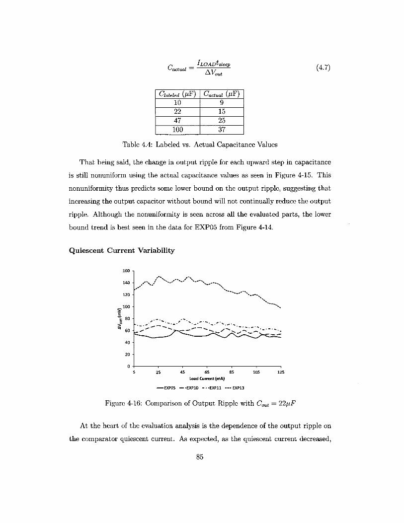
Cactuat = ILOADtsleepAV., (4.7)
Clabeled (pF) Cactual (pF)10 922 1547 25100 37
Table 4.4: Labeled vs. Actual Capacitance Values
That being said, the change in output ripple for each upward step in capacitance
is still nonuniform using the actual capacitance values as seen in Figure 4-15. This
nonuniformity thus predicts some lower bound on the output ripple, suggesting that
increasing the output capacitor without bound will not continually reduce the output
ripple. Although the nonuniformity is seen across all the evaluated parts, the lower
bound trend is best seen in the data for EXP05 from Figure 4-14.
Quiescent Current Variability
160
140
120
100
E8 80
a 60
40
20
0
I -*-
-. .-.-.
- .- . .
5 25 45 65 85Load Current (mA)
-EXP05 - -EXP10 - -- EXP1i --- EXP13
105 125
Figure 4-16: Comparison of Output Ripple with C., = 22pF
At the heart of the evaluation analysis is the dependence of the output ripple on
the comparator quiescent current. As expected, as the quiescent current decreased,
85

the output ripple increases, as seen in Figure 4-16. Since the built-in explicit DC
hysteresis is the same for all four parts, the increase in output ripple is predominately
the result of the increase in the sleep comparator propagation delay. Based on the
data, the increase in the propagation delay does not appear to scale at the same rate
as the decrease in the quiescent current.
80 -
60 - 00
550
40
030 -
20
10
00 10 20 30 40 50 60 70 80 90 100 110 120
Load Current (mA)
-10uF_EXP05 - - -1O0uF_EXP13 - -22uF_EXP10 -- 22uFEXPlI
Figure 4-17: Comparison of Output Ripple for Various Quiescent Current Levels andOutput Capacitors
Nevertheless, as seen in Figure 4-17, the effect of the increase in propagation delay
on output ripple can be mitigated by increasing the size of the output capacitor. From
the graph, the same average output ripple of EXP05 with an actual output capaci-
tance of 9pF can be achieved by EXP13, which operates at one-sixth of the original
by quadrupling the actual capacitance. For EXP11, which is operating at a quiescent
current level closest to the target value at one-third of the original value, the same
average output ripple can be achieved by doubling the actual output capacitance.
Based on the evaluation data, the output ripple generated by the propagation
delay appears to dominate over any built-in explicit DC hysteresis at the lower current
levels. Because of this, the final design does not contain any explicit DC hysteresis
and relies only on the intrinsic inertial hysteresis. This implementation thus decreases
the amount of switching noise in the first stage as well.
86
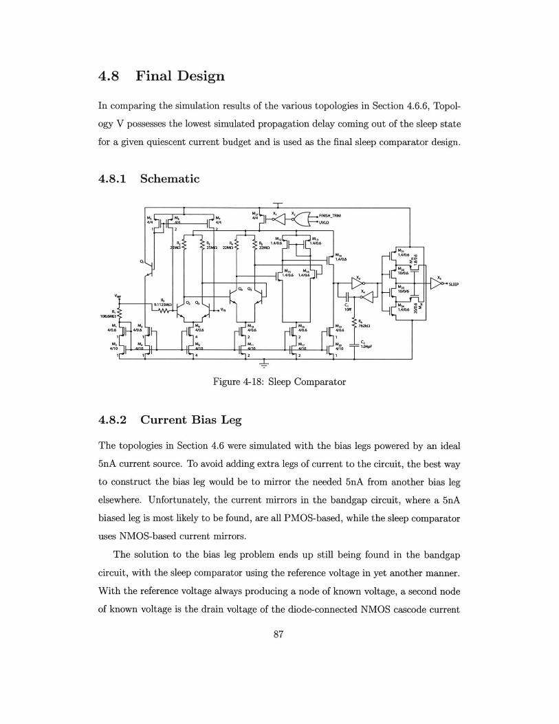
4.8 Final Design
In comparing the simulation results of the various topologies in Section 4.6.6, Topol-
ogy V possesses the lowest simulated propagation delay coming out of the sleep state
for a given quiescent current budget and is used as the final sleep comparator design.
4.8.1 Schematic
I -M, X X F1NtLTr4M
M7, 4/4414 UVLO
P. R, 1.4/Q6 T '.M49.625N n 22AAn A 22Mn
MIS 1.4/0.661.4/&6 c,
T
MI. M" A06210/0.6
1.4/&6 IA*6 10/0,6-- X5
Q. as Mn 5LEEP
4
Q3 C, M, 'R X)lX o 1 GA)/6
VFS I OfF 1.4/&6
C;W
1.416
we MIS MIS MIS 762knM 7624/0A QUA 4/0.6 410A
4 ? 2 2 1
M9 M71 M17 M20 C2
A/I& 4110 law
4 2 2 1
Figure 4-18: Sleep Comparator
4.8.2 Current Bias Leg
The topologies in Section 4.6 were simulated with the bias legs powered by an ideal
5nA current source. To avoid adding extra legs of current to the circuit, the best way
to construct the bias leg would be to mirror the needed 5nA from another bias leg
elsewhere. Unfortunately, the current mirrors in the bandgap circuit, where a 5nA
biased leg is most likely to be found, are all PMOS-based, while the sleep comparator
uses NMOS-based current mirrors.
The solution to the bias leg problem ends up still being found in the bandgap
circuit, with the sleep comparator using the reference voltage in yet another manner.
With the reference voltage always producing a node of known voltage, a second node
of known voltage is the drain voltage of the diode-connected NMOS cascode current
87
1 2
RZ
10U.Mn
1 1 -
M1 M4

source running at 5nA. Now, a resistor sized for a bias current of 5nA can be placed
between the to two to create the bias leg of the sleep comparator.
4.8.3 Simulated Results
tPHL 5.63pstPLH 13-93psAVou 14.6mV
ISLEEP,SUPPLY 50nA
Table 4.5: Sleep Comparator Simulation Data with VSUPPLY=5V, Cot=100pF,ILOAD=5OmA
Compared to the original LTC3588 biased at a total of 160nA, the new sleep com-
parator possesses a wake-up propagation delay that is not quite three times as large
while running at slightly less than one-third the original current level. In addition, it
meets the target total supply current allocation of 50nA from Chapter 2.
88

Chapter 5
Conclusion
5.1 Combined Simulated Results
In the two previous chapters, the new bandgap and sleep comparator blocks were
simulated as stand-alone blocks for the simulation results listed. Here, the bandgap
and sleep comparator blocks are simulated together to ensure that the connections
between the sleep comparator and the bandgap block do not significantly disrupt the
reference voltage node.
The bandgap reference voltage settles to 1.1814V as its final value.
VREF 1.1814VtPHL 5.84ps
tPLH 9.09psAV, 10.3mV
Table 5.1: Sleep Comparator Measurements with Bandgap Circuit with
VSUPPLY=3.5V, Cou=100pF, and ILOAD=5OmA
5.2 Recap and Future Work
In Chapters 3 and 4, new designs for the bandgap and sleep comparator blocks were
presented to fit the proposed work laid out in Chapter 1 of a converter system with
a no-load quiescent current level of 150nA. Because of the large difference between
89

the target current level and the lowest quiescent current level currently commercially
available, modified versions of the LTC3588 were fabricated with varying quiescent
current levels to evaluate the effect of low current operation, driven largely by the lack
of precise device modeling at the desired current levels. Nonetheless, even the current
device models show that the 5nA/leg implementation presented here is approaching
the limit of adequate device operation in the current technology, as evidenced by
the discussion on the impact of low 8 on the accuracy of the bandgap reference
voltage. Due to this lower limit, the quiescent current level certainly cannot continue
to decrease ad infinitum to zero.
Furthermore, over the course of the silicon evaluation of the modified LTC3588
chips, both benefits and disadvantages of low current operation were discovered. For
instance, although the efficiency at the lower current levels stayed at its maximum
value for a wider range of load currents (Figure 2-7), the output capacitor had to be
increased proportional to the first order with the quiescent current level reduction in
order to maintain the same output voltage ripple (Figure 4-17). Such performance
tradeoffs ultimately determine the breadth and types of applications for a converter
with ultra-low quiescent current.
In the future, until the lower limit has been reached, certain aspects of the system
presented here merit further study to push the quiescent current level even lower.
Currently, the weak bias blocks consume small amounts of "keep alive" current during
the sleep state in order to wake-up faster during the transition from the sleep to the
active state. These blocks can be examined to determine both the effectiveness of
such currents as well as the optimal combination, if any, of the weak bias current
and the response time. Similarly, while the intrinsic load current is not directly
counted towards the supply current, the output divider can be explored to find ways
of reducing this current without significantly sacrificing the response time of the
feedback node to perhaps increase the load current range with maximum converter
efficiency.
Even with simply the quiescent current reduction presented here, the converter
system discussed here already has the potential to further maximize the lifetime of
90

batteries in portable and remote battery-based applications beyond what is commer-
cially available today. Moreover, these applications range across a wide spread of
industries from manufacturing to biomedical devices to sensors.
91

92

Bibliography
[1] Chandrakasan, Anantha, Naveen Verma, and Denis C. Daly. "Ultralow-Power
Electronics for Biomedical Applications." Annual Review of Biomedical Engineer-
ing. 10. (2008): 247-275. Print.
[2] Linear Technology Corporation, Milpitas, CA. 42V, 2.5A, 2MHz Step-Down
Switching Regulator with 2.7pttA Quiescent Current, 2012. LT3975 Datasheet.
[3] Linear Technology Corporation, Milpitas, CA. 38V, 1.2A, 2MHz Step-Down Reg-
ulator with 2.8pA Quiescent Current, 2009. LT3971 Datasheet.
[4] Linear Technology Corporation, Milpitas, CA. 1.8pA Quiescent Current, 15V,
300mA Synchronous Step-Down DC/DC Converter, 2011. LTC3103 Datasheet.
[5] Linear Technology Corporation, Milpitas, CA. Piezoelectric Energy Harvesting
Power Supply, 2010. LTC3588-1 Datasheet.
[6] Linear Technology Corporation, Milpitas, CA. 20V High Efficiency Nanopower
Step Down Regulator, 2010. LTC3388-1 Datasheet.
[7] Kassakian, John G; Schelcht, Martin F; Verghese, George C. Principles of Power
Electronics. Addison Wesley, 1992.
[8] Gilbert, Barrie. Accurate Design of Low- Voltage, Low-Power Monolithic Refer-
ences. 1996. Print.
[9] Roulston, David J. Bipolar Semiconductor Devices. McGraw-Hill Companies,
1989. Print.
93

[10] del Alamo, Jesus A. Integrated Microelectronic Devices: Physics and Modeling,
Prentice Hall. 2011. Print.
[11] Liang, Yung C, and Samudra, Ganesh S. Power Microelectronics: Device and
Process Technologies. World Scientific Publishing Co, 2009.
[12] Hastings, Alan. Art of Analog Layout. Prentice Hall, 2nd edition, 2005.
[13] Neaman, Donald. Semiconductor Physics and Devices. Mc-Graw Hill Publishing,
2002. Print.
[14] Gardner, John U. Designing an Ultra Low Quiescent Current Buck Switching
Regulator, MIT, 2008.
94