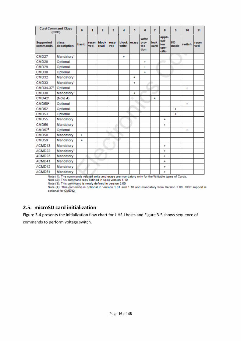
integral microsd card specification · sd bus allows dynamic configuration of the number of data...
TRANSCRIPT
Integral microSD Card
Specification MLC
Version 1.6
All rights are strictly reserved. Any portion of this paper shall not be reproduced, copied, or
translated to any other forms without permission from Integral Memory plc. Integral Memory plc
reserves the right to revise this documentation and to make changes to the content without
obligation of Integral Memory to provide notification of such change or revision. The Information
contained in this document is believed to be accurate; however it is preliminary information and
should not be relied upon for accuracy or completeness. Integral is a trademark of Integral Memory
plc. Other companies’ product or services that may be mentioned within this document may be
trademarks of their respective owners.
Integral Memory plc, Unit 6 Iron Bridge Close, Iron Bridge Business Park, London, NW10 0UF
Document Number: S-18306
Overview
Flash Type
Toshiba 15nm
Toshiba BiCS3
Toshiba BiCS4
WD-SanDisk BiCS3
Micron/SpecTek B05
Micron B16
Micron B17
Hynix 3D-V4
Bus Speed Mode
UHS-I
Speed Class
Class 10
A1
UHS-I, U1/U3
Up to V30
Power Consumption Note
Power Up Current < 250uA
Standby Current < 1000uA
Read Current < 400mA
Write Current < 400mA
Advanced Flash Management
ECC Correction
Static and Dynamic Wear Leveling
Bad Block Management
Write Protect with mechanical switch
Supply Voltage 2.7 ~ 3.6V
Temperature Range
Operation: -25°C ~ 85°C
Storage: -40°C ~ 85°C
RoHS compliant
EMI compliant
NOTE: Please see Chapter 5.1 Power Consumption for details.
Performance Overview
Capacity Class UHS-I VSC
APP
PERF
Class
Controller
Flash TestMetrix
A1 test
TestMetrix
Performance
Density Process Bit-per-
cell
Read
(IOPs)
Write
(IOPs)
Read
(MB/s)
Write
(MB/s)
2GB N/A N/A N/A PS8210 32Gbx1 15nm MLC N/A N/A 23.82 14.90
2GB N/A N/A N/A PS8039 32Gbx1 15nm MLC N/A N/A 23.98 14.59
4GB CL10 UHS-I
(Grade1) V10 N/A PS8039 32Gbx1 15nm MLC N/A N/A 84.59 15.73
8GB CL10 UHS-I
(Grade 1) V10 N/A PS8039 64Gbx1 15nm MLC N/A N/A 91.60 29.92
16GB CL10 UHS-I
(Grade 3) V30 N/A PS8039 64Gbx2 15nm MLC N/A N/A 90.37 54.78
32GB CL10 UHS-I
(Grade 3) V30 N/A PS8039 64Gbx4 15nm MLC N/A N/A 92.63 53.73

Table of Contents
1. Product Specifications................................................................................. 7
2. ELectrical Interface outlines ....................................................................... 9
2.1. microSD Card Pins........................................................................................................... 9
2.2. microSD Card Bus Topology ........................................................................................... 9
2.3. microSD Bus Mode Protocol ......................................................................................... 10
2.4. SPI Bus Mode Protocol .................................................................................................. 14
2.5. microSD card initialization ............................................................................................ 16
3. Environmental Specifications ................................................................... 19
3.1. Environmental Conditions ............................................................................................. 19
4. SD Card Comparison ................................................................................. 22
5. Electrical Specifications ............................................................................ 23
5.1. Power Consumption ....................................................................................................... 23
5.2. Working Rating .............................................................................................................. 24
5.3. DC Characteristic ........................................................................................................... 24
5.3.1. Bus Operation Conditions for 3.3V Signaling ................................................... 24
5.3.2. Bus Signal Line Load ......................................................................................... 25
5.3.3. Power Up Time of Host ..................................................................................... 26
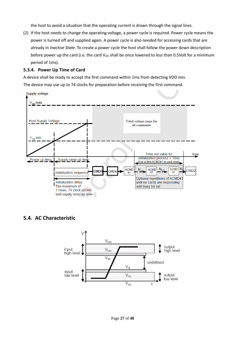
5.3.4. Power Up Time of Card ..................................................................................... 27
5.4. AC Characteristic ........................................................................................................... 27
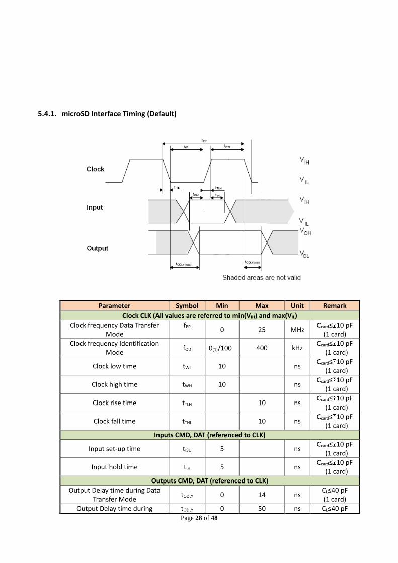
5.4.1. microSD Interface Timing (Default) .................................................................. 28
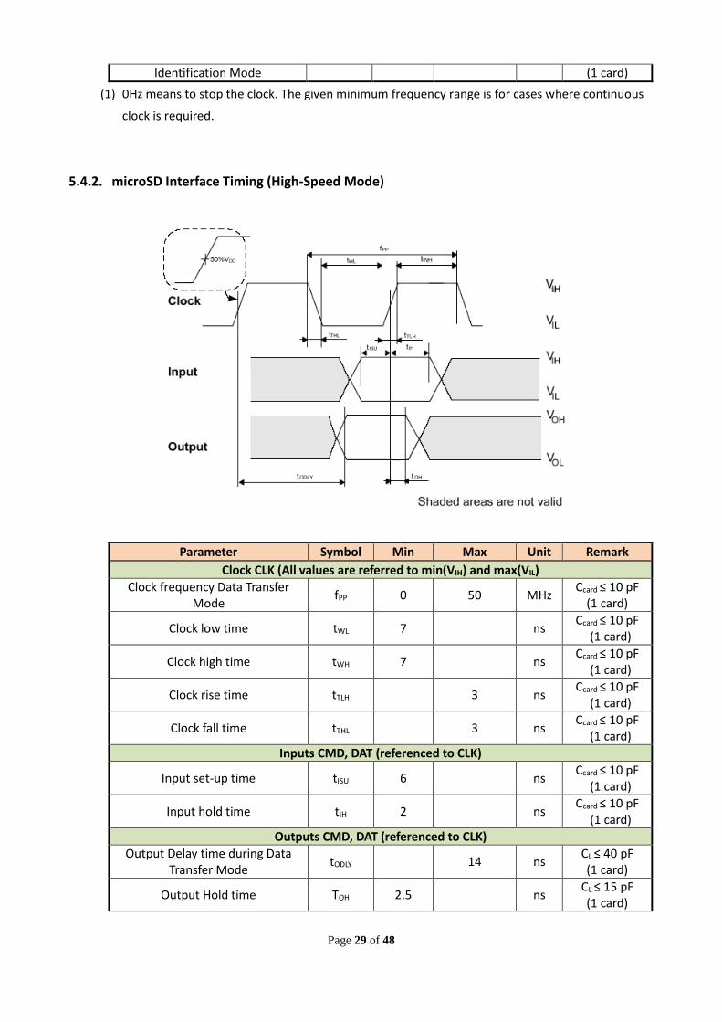
5.4.2. microSD Interface Timing (High-Speed Mode) ................................................ 29
5.4.3. microSD Interface Timing (SDR12, SDR25, SDR50 and SDR104 Modes) ..... 30
5.4.4. microSD Interface Timing (DDR50 Mode) ....................................................... 32
6. Host System Design Guildelines ............................................................... 33
6.1. Efficient Data Writing to microSD Memory Card ......................................................... 33
6.1.1. Write_Single_Block and Write_Multiple_Block ............................................... 33
6.2. Basic Process of Error Handling .................................................................................... 34
6.2.1. Retry Process...................................................................................................... 34
6.2.2. Recovery Process ............................................................................................... 34
6.2.3. Tuning Write Command Process ....................................................................... 34
6.2.4. Tuning Read Command Process ........................................................................ 34
6.2.5. Exception Handling Process .............................................................................. 34
6.3. Common Error Handling in SPI and SD mode .............................................................. 35

6.3.1. Time-out ............................................................................................................. 35
6.3.2. Error Detect (CMD CRC Error) ......................................................................... 35
6.3.3. Error Detect (Other Error) in SPI and SD mode ................................................ 35
6.3.4. Others ................................................................................................................. 35
6.4. Data Error Handling in SPI and SD mode ..................................................................... 35
6.4.1. Time-out ............................................................................................................. 35
6.4.2. Read CRC16 Error ............................................................................................. 35
6.4.3. Write CRC Status Error ..................................................................................... 35
6.4.4. Others ................................................................................................................. 35
6.5. Multiple Block Write (CMD25) Process ....................................................................... 36
6.6. Retry Error handling ...................................................................................................... 38
6.7. Recovery Error Handling ............................................................................................... 39
6.8. Tuning Write Command Error Handling ....................................................................... 40
6.9. Exception Error Handling .............................................................................................. 41
6.10. Multiple Blocks Read (CMD18) Error Handling Process ............................................. 42
6.11. Tuning Read Data Error Handling ................................................................................. 43
7. Registers ................................................................................................... 45
7.1. Card Registers ................................................................................................................ 45
8. Physical Dimension ................................................................................... 46
List of Tables
Table 3-1 microSD Memory Card Pad Assignment ........................................................ 9
Table 4-1 High-Temperature Test Condition ................................................................. 19
Table 4-2 Low-Temperature Test Condition .................................................................. 19
Table 4-3 High Humidity Test Condition ....................................................................... 19
Table 4-4 Shock Specification ......................................................................................... 20
Table 4-5 Vibration Specification ................................................................................... 20
Table 4-6 Drop Specification ........................................................................................... 20
Table 4-7 Bending Specification ...................................................................................... 20
Table 4-8 Torque Specification ........................................................................................ 20
Table 4-9 Mating Cycle Test Specification ..................................................................... 20
Table 4-10 ESD Specification .......................................................................................... 21
Table 5-1 Comparing microSDSC, microSDHC, and microSDXC ............................. 22
Table 5-2 Comparing UHS Speed Grade Symbols........................................................ 22
Table 6-1 Power Consumption of microSD card ........................................................... 23
Table 6-2 Threshold Level for High Voltage Range ...................................................... 24
Table 6-3 Peak Voltage and Leakage Current ............................................................... 24
Table 6-4 Threshold Level for 1.8V Signaling ............................................................... 25
Table 6-5 Input Leakage Current for 1.8V Signaling ................................................... 25
Table 5-6 Clock Signal Timing ........................................................................................ 30
Table 6-7 Output Timing of Fixed Data Window (SDR12, SDR25, SDR50) .............. 31
Table 6-8 Output Timing of Variable Window (SDR104) ............................................ 31
Table 6-9 Bus Timings – Parameters Values (DDR50 Mode) ....................................... 32

Page 7 of 48
1. PRODUCT SPECIFICATIONS
Compliant Specifications - SD Memory Card Specifications:
Compliant with Part 1 Physical Layer Specification Ver. 6.10
Compliant with Part 2 File System Specification Ver. 3.00
Compliant with Part 3 Security Specification Ver. 7.00
microSD Card Addendum Ver4.20
Support SD SPI mode
Bus Speed Mode (use 4 parallel data lines)
Non-UHS Mode
Default speed mode: 3.3V signaling, frequency up to 25MHz, up to 12.5 MB/sec
High speed mode: 3.3V signaling, frequency up to 50MHz, up to 25 MB/sec
UHS Mode
SDR12: SDR up to 25MHz, 1.8V signaling
SDR25: SDR up to 50MHz, 1.8V signaling
SDR50: 1.8V signaling, frequency up to 100MHz, up to 50 MB/sec
SDR104: 1.8V signaling, frequency up to 208MHz, up to 104MB/sec
DDR50: 1.8V signaling, frequency up to 50MHz, sampled on both clock edges, up to 50
MB/sec
NOTES: 1. Timing in 1.8V signaling is different from that of 3.3V signaling.
2. To properly run the UHS mode, please ensure the device supports UHS-I mode.
The command list supports [Part 1 Physical Layer Specification Ver. 6.10 ] definitions
Command list are described in “Table 3-2 SD mode Command Set ” and “Table 3-3 SPI
mode Command Set” in this document
Copyrights Protection Mechanism
Compliant with Part 1 Physical Layer Specification ver. 6.10, CPRM is Optional in
microSDHC/microSDXC.
Support Hot Plug
Card removal during read operation will never harm the content
Password Protection of cards (optional)
Designed for read intensive and write intensive cards
Built-in write protection features (permanent and temporary)
Write Protect feature using mechanical switch (Full SD Card only)
Page 8 of 48
Electrostatic Discharge(ESD)
ESD protection in pads (contact discharge).
ESD protection in non-contact pad area (air discharge).
Operation voltage range: 2.7V ~ 3.6V
Temperature Range
Operation Temp. Range: -25~85
Storage Temp. Range: -40~85
Page 9 of 48
2. ELECTRICAL INTERFACE OUTLINES
2.1. microSD Card Pins
Figure 3-1 microSD Card Pin assignment (Back View of the card)
Table 3-1 microSD Memory Card Pad Assignment
pin SD Mode SPI Mode
Name Type1 Description Name Type Description
1 DAT2 I/O/PP Data Line [bit2] RSV
2 CD/DAT3 2 I/O/PP 3 Card Detect/
Data Line [bit3] CS I 3 Chip Select (neg. true)
3 CMD PP Command/Response DI I Data In
4 VDD S Supply voltage VDD S Supply voltage
5 CLK I Clock SCLK I Clock
6 VSS S Supply voltage ground VSS S Supply voltage ground
7 DAT0 I/O/PP Data Line [bit0] DO O/PP Data Out
8 DAT1 I/O/PP Data Line [bit1] RSV
(1) S: power supply, I: input; O: output using push-pull drivers; PP: I/O using push-pull drivers.
(2) The extended DAT lines (DAT1-DAT3) are input on power up. They start to operate as DAT lines after
SET_BUS_WIDTH command. The Host shall keep its own DAT1-DAT3 lines in input mode as well while
they are not used. It is defined so in order to keep compatibility to MultiMedia Cards.
(3) At power up, this line has a 50KOhm pull up enabled in the card. This resistor serves two functions: Card
detection and Mode Selection. For Mode Selection, the host can drive the line high or let it be pulled
high to select SD mode. If the host wants to select SPI mode, it should drive the line low. For Card
detection, the host detects that the line is pulled high. This pull-up should be disconnected by the user
during regular data transfer with SET_CLR_CARD_DETECT (ACMD42) command.
2.2. microSD Card Bus Topology The microSD card supports 2 alternative communication protocols, SD and SPI BUS mode.
Page 10 of 48
Host can choose either one of both bus mode, same data can be read or written by both modes.
SD mode allows 4-bits data transfer way, it provides high performance. SPI mode supports 1-bit data
transfer and of course the performance is lower compared to SD mode.
2.3. microSD Bus Mode Protocol In default speed, the microSD Memory Card bus has a single master (application); multiple slaves (Cards),
synchronous star topology (refer to Figure 3-2). In high speed and UHS-I, the microSD Memory Card bus has
a single master (application) and single slave (card), synchronous point to point topology. Clock, power and
ground signals are common to all cards. Command (CMD) and data (DAT0-DAT3) signals are dedicated to
each card providing continues point to point connection to all the cards.
During initialization process commands are sent to each card individually, allowing the application to detect
the cards and assign logical addresses to the physical slots. Data is always sent (received) to (from) each
card individually. However, in order to simply the handling of the card stack, after the initialization process,
all commands may be sent concurrently to all cards. Addressing information is provided in the command
packet.
SD bus allows dynamic configuration of the number of data lines. After power up, by default, the microSD
Memory Card will use only DAT0 for data transfer. After initialization the host can change the bus width
(number of data active lines). This feature allows easy tradeoff between HW cost and system performance.
Note that while DAT1 to DAT3 are not in use, the related Host’s DAT lines should be in tri-state (input
mode). For SDIO cards DAT1 and DAT2 are used for signaling.
Figure 3-2 SD Memory Card System Bus Topology
The microSD bus includes the following signals:
CLK: Host to card clock signal
CMD: Bidirectional Command/Response signal
DAT0-DAT3: 4 Bidirectional data signals

Page 11 of 48
VDD, Vss1, Vss2: Power and ground signals
Table 3-2 SD Mode Command Set

Page 12 of 48

Page 13 of 48

Page 14 of 48
2.4. SPI Bus Mode Protocol While the SD Memory Card channel is based on command and data bit streams that are initiated by a start
bit and terminated by a stop bit, the SPI channel by byte oriented. Every command or data block is built for
8-bit bytes and is byte aligned with the CS signal (i.e. the length is a multiple of 8 clock cycles). The card
starts to count SPI bus clock cycle at the assertion of the CS signal. Every command or data token shall be
aligned with 8-clock cycle boundary.
Similar to the SD Memory Card Protocol, the SPI messages consist of command, response and data-block
tokens.
The advantage of SPI mode is reducing the host design effort, especially for MMC host side, it just be
modified by little change. Note: please use SD card specification to implement SPI mode function, not use
MMC specification. For example, SPI mode is initialized by ACMD41, and the registers are different from
MMC card, especially CSD register.
Figure 3-3 SD Memory Card State Diagram (SPI mode)
Page 15 of 48
Table 3-3 SPI Mode Command Set
Page 16 of 48
2.5. microSD card initialization Figure 3-4 presents the initialization flow chart for UHS-I hosts and Figure 3-5 shows sequence of
commands to perform voltage switch.
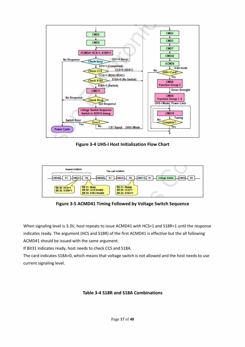
Page 17 of 48
Figure 3-4 UHS-I Host Initialization Flow Chart
Figure 3-5 ACMD41 Timing Followed by Voltage Switch Sequence
When signaling level is 3.3V, host repeats to issue ACMD41 with HCS=1 and S18R=1 until the response
indicates ready. The argument (HCS and S18R) of the first ACMD41 is effective but the all following
ACMD41 should be issued with the same argument.
If Bit31 indicates ready, host needs to check CCS and S18A.
The card indicates S18A=0, which means that voltage switch is not allowed and the host needs to use
current signaling level.
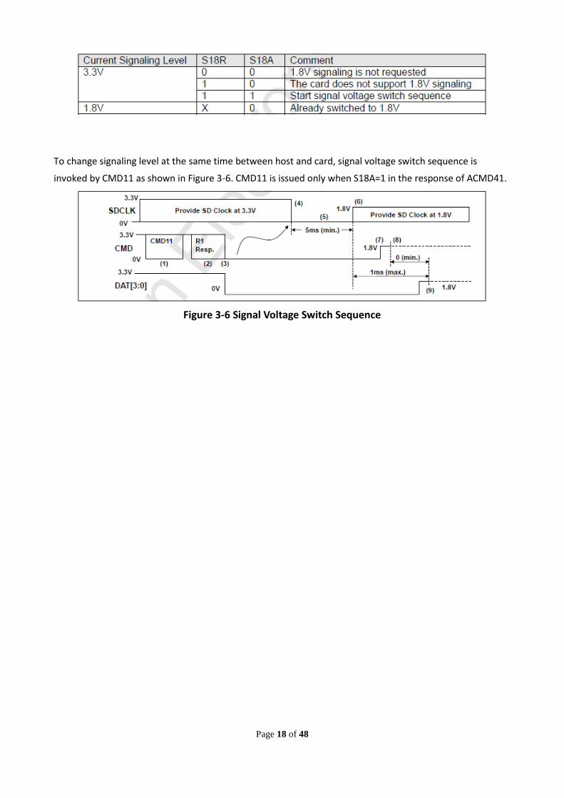
Table 3-4 S18R and S18A Combinations
Page 18 of 48
To change signaling level at the same time between host and card, signal voltage switch sequence is
invoked by CMD11 as shown in Figure 3-6. CMD11 is issued only when S18A=1 in the response of ACMD41.
Figure 3-6 Signal Voltage Switch Sequence
Page 19 of 48
3. ENVIRONMENTAL SPECIFICATIONS
3.1. Environmental Conditions
Temperature and Humidity
Temperature Range
Operational: -25°C ~ 85°C
Storage: -40°C ~ 85°C
Humidity
Operational: RH = 95% under 25°C
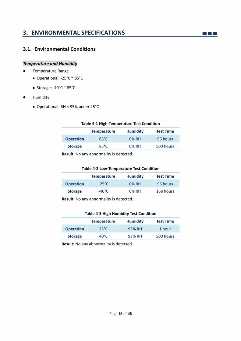
Table 4-1 High-Temperature Test Condition
Temperature Humidity Test Time
Operation 85°C 0% RH 96 hours
Storage 85°C 0% RH 500 hours
Result: No any abnormality is detected.
Table 4-2 Low-Temperature Test Condition
Temperature Humidity Test Time
Operation -25°C 0% RH 96 hours
Storage -40°C 0% RH 168 hours
Result: No any abnormality is detected.
Table 4-3 High Humidity Test Condition
Temperature Humidity Test Time
Operation 25°C 95% RH 1 hour
Storage 40°C 93% RH 500 hours
Result: No any abnormality is detected.

Page 20 of 48
Shock
Table 4-4 Shock Specification
Acceleration Force Half Sin Pulse Duration
microSD card 500G 0.5ms
Result: No any abnormality is detected when power on.
Vibration
Table 4-5 Vibration Specification
Condition Vibration Orientation
Frequency/Displacement Frequency/Acceleration
microSD card 20Hz~80Hz/1.52mm 80Hz~2000Hz/20G Direction: X, Y, Z axis
Duration: 30 min/direction
Result: No any abnormality is detected when power on.
Drop
Table 4-6 Drop Specification
Height of Drop Number of Drops
microSD card 150cm free fall Direction: 6 face; 1 time/face
Result: No any abnormality is detected when power on.
Bending
Table 4-7 Bending Specification
Force Action
microSD card ≥ 10N Hold for 1min; total 5 times.
Result: No any abnormality is detected when power on.
Torque
Table 4-8 Torque Specification
Force Action
microSD card 0.1N-m or ±2.5 deg Hold 30 second/direction
Total 5 cycles
Result: No any abnormality is detected when power on.
Durability Mating Cycle Test
Table 4-9 Mating Cycle Test Specification
Number of Mating Cycle
microSD card 10,000 cycles
Page 21 of 48
Result: No any abnormality is detected when power on.
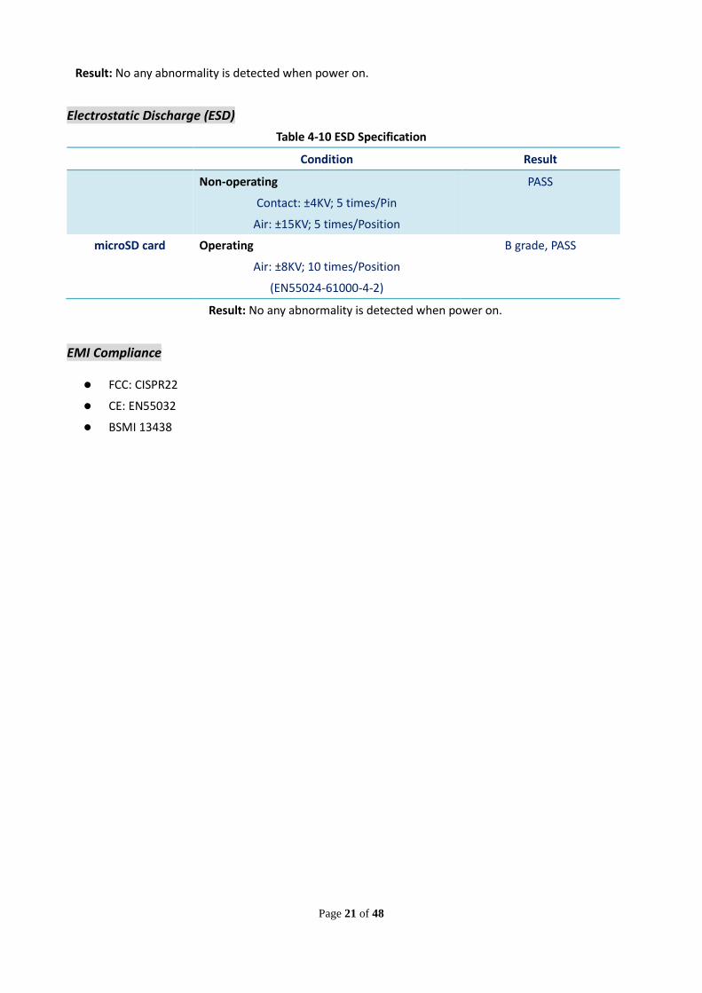
Electrostatic Discharge (ESD)
Table 4-10 ESD Specification
Condition Result
Non-operating
Contact: ±4KV; 5 times/Pin
Air: ±15KV; 5 times/Position
PASS
microSD card Operating
Air: ±8KV; 10 times/Position
(EN55024-61000-4-2)
B grade, PASS
Result: No any abnormality is detected when power on.
EMI Compliance
FCC: CISPR22
CE: EN55032
BSMI 13438
Page 22 of 48
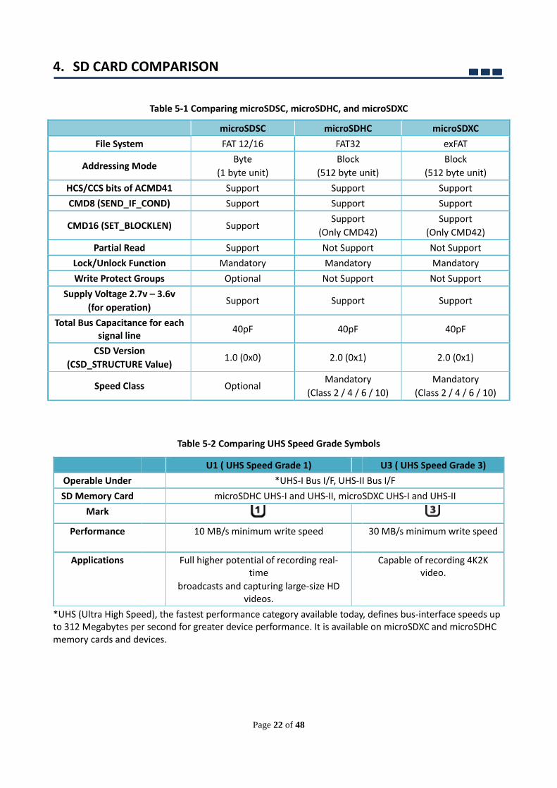
4. SD CARD COMPARISON
Table 5-1 Comparing microSDSC, microSDHC, and microSDXC
Table 5-2 Comparing UHS Speed Grade Symbols
*UHS (Ultra High Speed), the fastest performance category available today, defines bus-interface speeds up to 312 Megabytes per second for greater device performance. It is available on microSDXC and microSDHC memory cards and devices.
microSDSC microSDHC microSDXC
File System FAT 12/16 FAT32 exFAT
Addressing Mode Byte
(1 byte unit)
Block
(512 byte unit)
Block
(512 byte unit)
HCS/CCS bits of ACMD41 Support Support Support
CMD8 (SEND_IF_COND) Support Support Support
CMD16 (SET_BLOCKLEN) Support Support
(Only CMD42)
Support
(Only CMD42)
Partial Read Support Not Support Not Support
Lock/Unlock Function Mandatory Mandatory Mandatory
Write Protect Groups Optional Not Support Not Support
Supply Voltage 2.7v – 3.6v
(for operation) Support Support Support
Total Bus Capacitance for each signal line
40pF 40pF 40pF
CSD Version
(CSD_STRUCTURE Value) 1.0 (0x0) 2.0 (0x1) 2.0 (0x1)
Speed Class Optional Mandatory
(Class 2 / 4 / 6 / 10)
Mandatory
(Class 2 / 4 / 6 / 10)
U1 ( UHS Speed Grade 1) U3 ( UHS Speed Grade 3)
Operable Under *UHS-I Bus I/F, UHS-II Bus I/F
SD Memory Card microSDHC UHS-I and UHS-II, microSDXC UHS-I and UHS-II
Mark
Performance
10 MB/s minimum write speed 30 MB/s minimum write speed
Applications
Full higher potential of recording real-time
broadcasts and capturing large-size HD videos.
Capable of recording 4K2K video.

Page 23 of 48
5. ELECTRICAL SPECIFICATIONS
5.1. Power Consumption
The table below is the power consumption of microSD card with different flash memory types.
Table 6-1 Power Consumption of microSD card
Flash Mode
Max. Power
Up Current
(uA)
Max. Standby
Current (uA)
Max. Read
Current (mA)
Max. Write
Current (mA)
Default Speed Mode 250 1000 150 @ 3.6V 150 @ 3.6V
High Speed Mode 250 1000 200 @ 3.6V 200 @ 3.6V
UHS-I
Mode
UHS50/DDR50 250 1000 400 @ 3.6V 400 @ 3.6V
UHS104/ DDR50 250 1000 400 @ 3.6V 400 @ 3.6V
NOTES:
1. Power consumptions are measured at room temperature.
Page 24 of 48
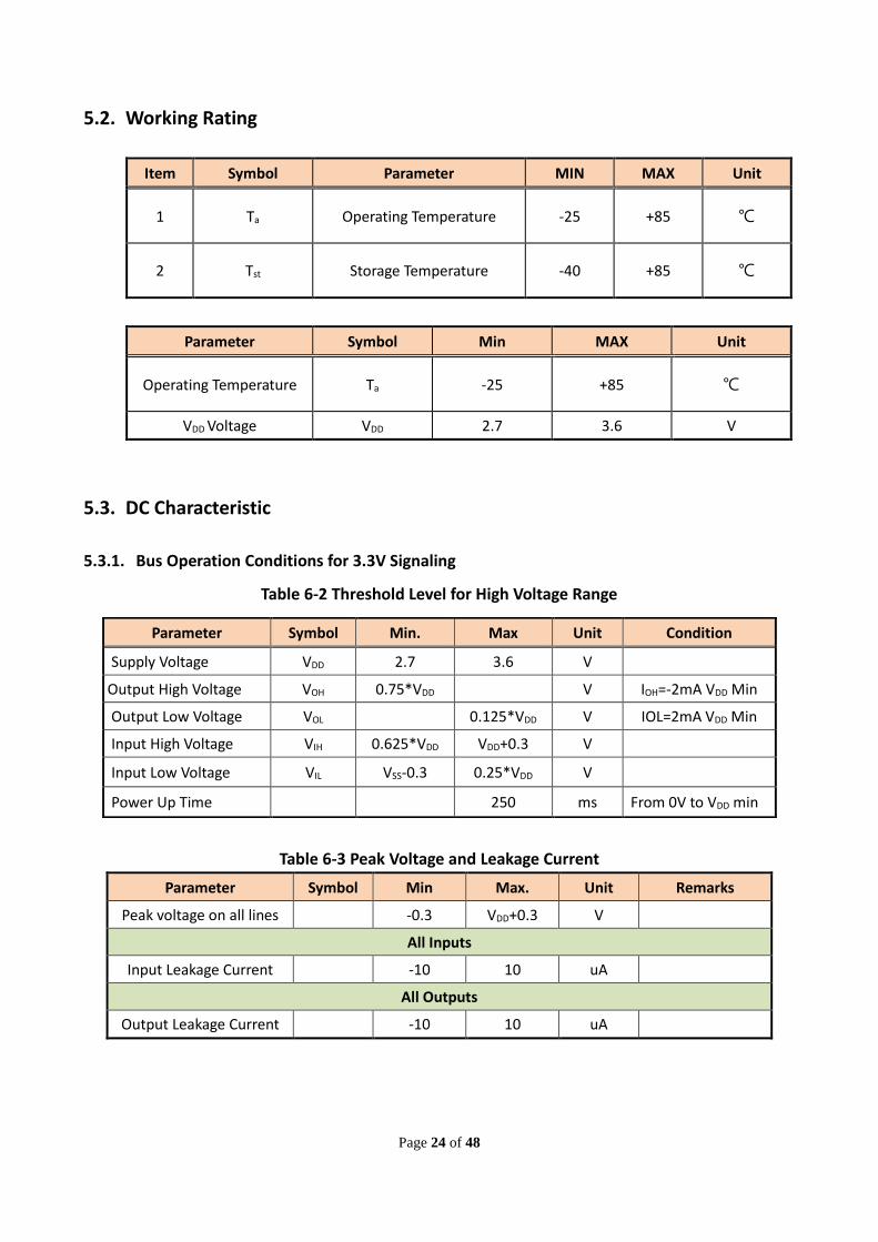
5.2. Working Rating
Item Symbol Parameter MIN MAX Unit
1 Ta Operating Temperature -25 +85
2 Tst Storage Temperature -40 +85
Parameter Symbol Min MAX Unit
Operating Temperature Ta -25 +85
VDD Voltage VDD 2.7 3.6 V
5.3. DC Characteristic
5.3.1. Bus Operation Conditions for 3.3V Signaling
Table 6-2 Threshold Level for High Voltage Range
Table 6-3 Peak Voltage and Leakage Current
Parameter Symbol Min Max. Unit Remarks
Peak voltage on all lines -0.3 VDD+0.3 V
All Inputs
Input Leakage Current -10 10 uA
All Outputs
Output Leakage Current -10 10 uA
Parameter Symbol Min. Max Unit Condition
Supply Voltage VDD 2.7 3.6 V
Output High Voltage VOH 0.75*VDD V IOH=-2mA VDD Min
Output Low Voltage VOL 0.125*VDD V IOL=2mA VDD Min
Input High Voltage VIH 0.625*VDD VDD+0.3 V
Input Low Voltage VIL VSS-0.3 0.25*VDD V
Power Up Time 250 ms From 0V to VDD min
Page 25 of 48
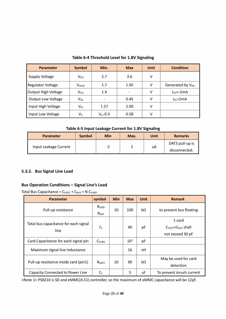
Table 6-4 Threshold Level for 1.8V Signaling
Table 6-5 Input Leakage Current for 1.8V Signaling
Parameter Symbol Min Max. Unit Remarks
Input Leakage Current -2 2 uA DAT3 pull-up is
disconnected.
5.3.2. Bus Signal Line Load
Bus Operation Conditions – Signal Line’s Load
Total Bus Capacitance = CHOST + CBUS + N CCARD
Parameter symbol Min Max Unit Remark
Pull-up resistance RCMD
RDAT 10 100 kΩ to prevent bus floating
Total bus capacitance for each signal
line CL 40 pF
1 card
CHOST+CBUS shall
not exceed 30 pF
Card Capacitance for each signal pin CCARD 101 pF
Maximum signal line inductance 16 nH
Pull-up resistance inside card (pin1) RDAT3 10 90 kΩ May be used for card
detection
Capacity Connected to Power Line CC 5 uF To prevent inrush current
<Note 1> PS8210 is SD and eMMC(4.51) controller, so the maximum of eMMC capacitance will be 12pF.
Parameter Symbol Min. Max Unit Condition
Supply Voltage VDD 2.7 3.6 V
Regulator Voltage VDDIO 1.7 1.95 V Generated by VDD
Output High Voltage VOH 1.4 - V IOH=-2mA
Output Low Voltage VOL - 0.45 V IOL=2mA
Input High Voltage VIH 1.27 2.00 V
Input Low Voltage VIL Vss-0.3 0.58 V

Page 26 of 48
5.3.3. Power Up Time of Host
The host needs to keep power line level less than 0.5V and more than 1ms before power ramp up.
Power On or Power Cycle
Followings are requirements for Power on and Power cycle to assure a reliable microSD Card hard reset.
(1) Voltage level shall be below 0.5V.
(2) Duration shall be at least 1ms.
Power Supply Ramp Up
The power ramp up time is defined from 0.5V threshold level up to the operating supply voltage which is
stable between VDD (min.) and VDD (max.) and host can supply SDCLK.
Followings are recommendations of Power ramp up:
(1) The voltage of power ramp up should be monotonic as much as possible.
(2) The minimum ramp up time should be 0.1ms.
(3) The maximum ramp up time should be 35ms for 2.7-3.6V power supply. (4) Host shall wait until VDD is stable. (5) After 1ms VDD stable time, the host provides at least 74 clocks before issuing the first command.
Power Down and Power Cycle
(1) When the host shuts down the power, the card VDD shall be lowered to less than 0.5Volt for a minimum
period of 1ms. During power down, DAT, CMD, and CLK should be disconnected or driven to logical 0 by
Page 27 of 48
the host to avoid a situation that the operating current is drawn through the signal lines.
(2) If the host needs to change the operating voltage, a power cycle is required. Power cycle means the
power is turned off and supplied again. A power cycle is also needed for accessing cards that are
already in Inactive State. To create a power cycle the host shall follow the power down description
before power up the card (i.e. the card VDD shall be once lowered to less than 0.5Volt for a minimum
period of 1ms).
5.3.4. Power Up Time of Card
A device shall be ready to accept the first command within 1ms from detecting VDD min.
The device may use up to 74 clocks for preparation before receiving the first command.
5.4. AC Characteristic
Page 28 of 48
5.4.1. microSD Interface Timing (Default)
Parameter Symbol Min Max Unit Remark
Clock CLK (All values are referred to min(VIH) and max(VIL)
Clock frequency Data Transfer Mode
fPP
0 25 MHz Ccard≤ 10 pF
(1 card)
Clock frequency Identification Mode
fOD 0(1)/100 400 kHz Ccard≤ 10 pF
(1 card)
Clock low time tWL 10 ns Ccard≤ 10 pF
(1 card)
Clock high time tWH 10 ns Ccard≤ 10 pF
(1 card)
Clock rise time tTLH 10 ns Ccard≤ 10 pF
(1 card)
Clock fall time tTHL 10 ns Ccard≤ 10 pF
(1 card)
Inputs CMD, DAT (referenced to CLK)
Input set-up time tISU 5 ns Ccard≤ 10 pF
(1 card)
Input hold time tIH 5 ns Ccard≤ 10 pF
(1 card)
Outputs CMD, DAT (referenced to CLK)
Output Delay time during Data Transfer Mode
tODLY 0 14 ns CL≤40 pF (1 card)
Output Delay time during tODLY 0 50 ns CL≤40 pF
Page 29 of 48
Identification Mode (1 card)
(1) 0Hz means to stop the clock. The given minimum frequency range is for cases where continuous
clock is required.
5.4.2. microSD Interface Timing (High-Speed Mode)
Parameter Symbol Min Max Unit Remark
Clock CLK (All values are referred to min(VIH) and max(VIL)
Clock frequency Data Transfer Mode
fPP 0 50 MHz Ccard ≤ 10 pF
(1 card)
Clock low time tWL 7 ns Ccard ≤ 10 pF
(1 card)
Clock high time tWH 7 ns Ccard ≤ 10 pF
(1 card)
Clock rise time tTLH 3 ns Ccard ≤ 10 pF
(1 card)
Clock fall time tTHL 3 ns Ccard ≤ 10 pF
(1 card)
Inputs CMD, DAT (referenced to CLK)
Input set-up time tISU 6 ns Ccard ≤ 10 pF
(1 card)
Input hold time tIH 2 ns Ccard ≤ 10 pF
(1 card)
Outputs CMD, DAT (referenced to CLK)
Output Delay time during Data Transfer Mode
tODLY 14 ns CL ≤ 40 pF (1 card)
Output Hold time TOH 2.5 ns CL ≤ 15 pF (1 card)

Page 30 of 48
Total System capacitance of each line¹
CL 40 pF CL ≤ 15 pF
(1 card)
(1) In order to satisfy severe timing, the host shall drive only one card.
5.4.3. microSD Interface Timing (SDR12, SDR25, SDR50 and SDR104 Modes)
Input
Table 5-6 Clock Signal Timing
Symbol Min Max Unit Remark
tCLK 4.80 - ns 208MHz (Max.), Between rising edge, VCT= 0.975V
tCR, tCF - 0.2* tCLK ns
tCR, tCF < 0.96ns (max.) at 208MHz, CCARD=10pF tCR, tCF < 2.00ns (max.) at 100MHz, CCARD=10pF
The maximum value of tCR, tCF is 10ns regardless of clock frequency
Clock Duty 30 70 %
SDR50 and SDR104 Input Timing
Symbol Min Max Unit SDR104 Mode
tIS 1.40 - ns CCARD =10pF, VCT= 0.975V
tIH 0.801 - ns CCARD = 5pF, VCT= 0.975V
Symbol Min Max Unit SDR50 Mode
tIS 3.00 - ns CCARD =10pF, VCT= 0.975V
tIH 0.801 - ns CCARD = 5pF, VCT= 0.975V
<Note 1> PS8210 is SD and eMMC(4.51) controller, so the maximum CCARD becomes 12pF and minimum of tIH will be 1.10 ns.
Page 31 of 48
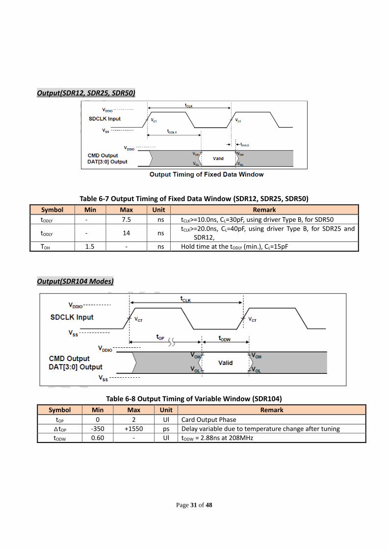
Output(SDR12, SDR25, SDR50)
Table 6-7 Output Timing of Fixed Data Window (SDR12, SDR25, SDR50)
Symbol Min Max Unit Remark
tODLY - 7.5 ns tCLK>=10.0ns, CL=30pF, using driver Type B, for SDR50
tODLY - 14 ns tCLK>=20.0ns, CL=40pF, using driver Type B, for SDR25 and
SDR12,
TOH 1.5 - ns Hold time at the tODLY (min.), CL=15pF
Output(SDR104 Modes)
Table 6-8 Output Timing of Variable Window (SDR104)
Symbol Min Max Unit Remark
tOP 0 2 Ul Card Output Phase
tOP -350 +1550 ps Delay variable due to temperature change after tuning
tODW 0.60 - Ul tODW = 2.88ns at 208MHz

Page 32 of 48
5.4.4. microSD Interface Timing (DDR50 Mode)
Symbol Min Max Unit Remark
tCLK 20 - ns 50MHz (Max.), Between rising edge
tCR, tCF - 0.2* tCLK ns tCR, tCF < 4.00ns (max.) at 50MHz, CCARD=10pF
Clock Duty 45 55 %
Table 6-9 Bus Timings – Parameters Values (DDR50 Mode)
Parameter Symbol Min Max Unit Remark
Input CMD (referenced to CLK rising edge)
Input set-up time tISU 3 - ns Ccard≤ 10 pF
(1 card)
Input hold time tIH 0.8 - ns Ccard≤ 10 pF
(1 card)
Output CMD (referenced to CLK rising edge)
Output Delay time during Data Transfer Mode
tODLY 13.7 ns CL≤30 pF (1 card)
Output Hold time TOH 1.5 - ns CL≥15 pF
Page 33 of 48
(1 card)
Inputs DAT (referenced to CLK rising and falling edges)
Input set-up time tISU2x 3 - ns Ccard≤ 10 pF
(1 card)
Input hold time tIH2x 0.8 - ns Ccard≤ 10 pF
(1 card)
Outputs DAT (referenced to CLK rising and falling edges)
Output Delay time during Data Transfer Mode
tODLY2x - 7.0 ns CL≤25 pF (1 card)
Output Hold time TOH2x 1.5 - ns CL≥15 pF (1 card)
6. HOST SYSTEM DESIGN GUILDELINES
6.1. Efficient Data Writing to microSD Memory Card
In order to optimize sequential writing performance and WAF (Write Amplification Factor), it is
recommended to use allocation unit (AU) writing.
It is recommended that Multiple_Block_Write shall be used as a command for writing data, and the size of
data written by each command should be the FAT cluster x n (n: integer)
6.1.1. Write_Single_Block and Write_Multiple_Block
Write single block (CMD24) was written by one sector (512Bytes), which is suitable to write small area such
like updating file system area (FAT). Besides, Write multiple blocks (CMD25) is a command for writing data
to blocks that have sequential address per command, which is suitable to write large area such as user data.
Write multiple blocks with a cluster unit (512Byte x 128 Sectors = 64KByte) in the file system is an efficient
access to the flash memory, it is obviously to provide higher speed to compared to single write block.
And it could be estimated that microSD card internal process would be reduced to save power consumption
and flash write amplification factor, that is why the efficient data writing was recommended. To avoid the
command issued by 512Bytes with single write block, software processes in the host device become faster.
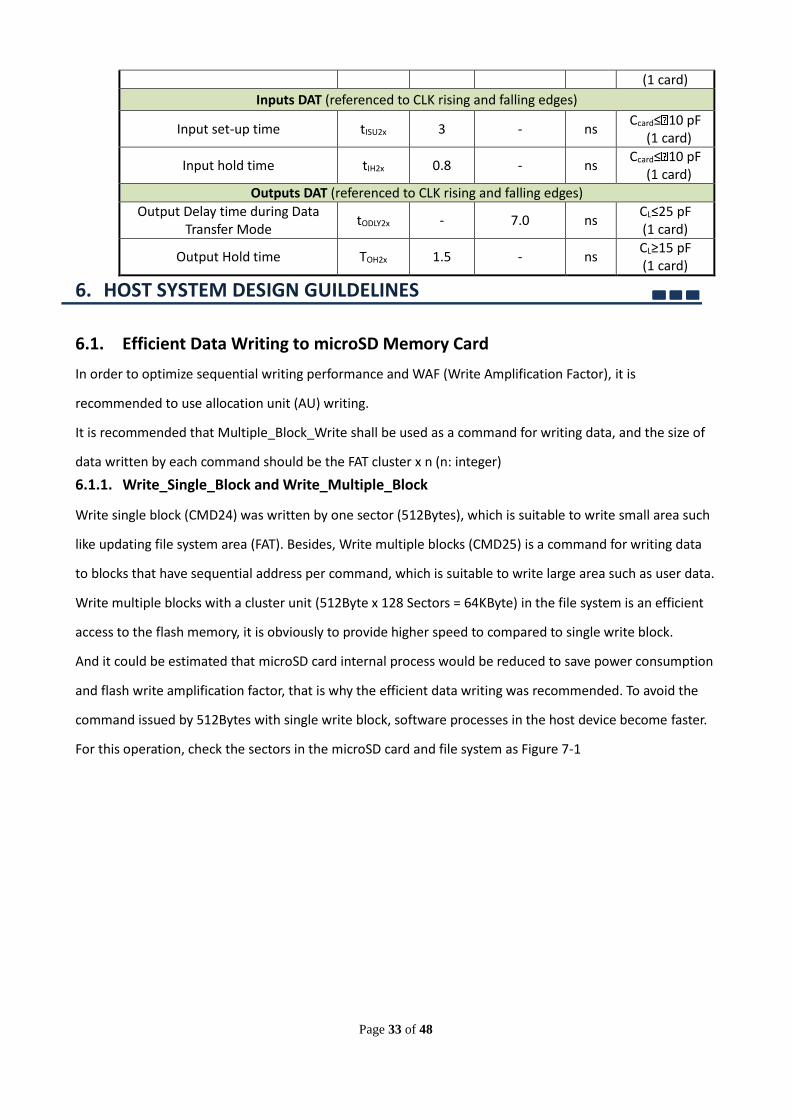
For this operation, check the sectors in the microSD card and file system as Figure 7-1
Page 34 of 48
Figure 7-1 Matching between logical address and file system
Note: Large Cluster unit is better for performance and WAF, for example, 128KB, 256KB or 512KB. Large
cluster unit also can save write command numbers and few transfer time.
6.2. Basic Process of Error Handling
6.2.1. Retry Process
Execute the process by sending commands again, especially for signal issue between card and host.
6.2.2. Recovery Process
Confirm card status is in Transfer State, if card status is not in Transfer State, please issue Stop command to
recover it and execute or continue flow. If there was UECC during read/write status, we could use recovery
process to recover it.
6.2.3. Tuning Write Command Process
In order to adjust Host CMD and CLK timing, the way is issue tuning command to confirm what the device
response and data was received by host. Based on the response, host was adjusting the timing step by step
and recording the pass range. Through this flow host could adjust the appropriate timing settings to avoid
unexpected handshaking issue.
6.2.4. Tuning Read Command Process
In order to adjust Host CLK and DAT timing, the way is issue tuning command to confirm what the device
response and data was received by host. Based on the response, host was adjusting the timing step by step
and recording the pass range. Through this flow host could adjust the appropriate timing settings to avoid
unexpected handshaking issue.
6.2.5. Exception Handling Process
No doubt that sometimes we would face all error handling above could not recover it successfully, and we

Page 35 of 48
could react based on the situation.
- If there was error in response, we could re-initialize the card.
- If it was signal issue, we could set up signal status by reading data and tuning command.
6.3. Common Error Handling in SPI and SD mode
6.3.1. Time-out
Run the Retry Process. No response from CMD, it might be signal or status got problem. To avoid the infinite
loop, implement a retry counter in the host so that, if the retry counter expires, the exception handling
starts in the host.
6.3.2. Error Detect (CMD CRC Error)
Run the Recovery Process. If it got second time failure with CRC, the setting might be too margin to receive
response stably. Suggestion is use tuning write command to fix timing and then retry it.
6.3.3. Error Detect (Other Error) in SPI and SD mode
Run the Recovery Process.
6.3.4. Others
Most errors could be recovered by running the Recovery Process, let card come into Transfer State and then
executing the flow we planned. If it does not work, please use exception method to come back initial state.
6.4. Data Error Handling in SPI and SD mode
6.4.1. Time-out
Run the Recovery Process. While the state was recovered, run the flow again.
6.4.2. Read CRC16 Error
Run the Recovery Process. If it got second time failure with CRC, the setting might be too margin to receive
data stably. Suggestion is use tuning read date to fix timing and then retry it.
6.4.3. Write CRC Status Error
Run the Recovery Process. If it got second time failure with CRC, the setting might be too margin to receive
CRC status stably. Suggestion is use tuning read date to fix timing and then retry it.
6.4.4. Others
Most errors could be recovered by running the Recovery Process, let card come into Transfer State and then
executing the flow we planned.

Page 36 of 48
6.5. Multiple Block Write (CMD25) Process - If Response is ADDRESS_OUT_OF_RANGE, please confirm writing address.
- If Response is DEVICE_IS_LOCKED, please stop writing data.
- If Response is COM_CRC_ERROR, run retry or tuning.
CMD25
CommandResponse
ResponseCRC7
Recovery
Retry
Send Data
CRC status
TransferEnd
CMD12
CMD13
CommandResponse
CommandResponse
Finish
Pass
TimeoutError
Not match
Pass
No
Yes
Pass
Pass
ErrorTimeout
Recovery Tunning Write
Command
Fail
ErrorTimeout
Programstate Over SPEC
timeout
No
Recovery Yes
Figure 7-2 Multiple Write (CMD25) Error Handling

Page 37 of 48
Page 38 of 48
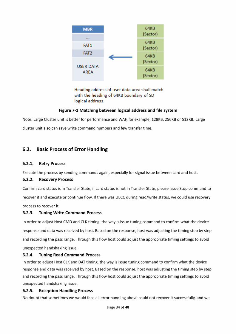
6.6. Retry Error handling In order to avoid signal issue caused unexpected response from device, we could use Retry Process to fix it.
- Please make sure card state is in transfer state before issuing following commands.
- To avoid the infinite loop, implement a retry counter in the host.
- If the device could not respond to CMD13 normally, please run exception handling to recover card
status.
CMD13
CommandResponse
Decrease retry count
Exception handle
CheckState
Pass
TimeoutError
Other state
Transfer state
More than 0
Equal to 0
Re-send command before retry process
Figure 7-3 Retry Error Handling Process

Page 39 of 48
6.7. Recovery Error Handling Sometimes the device failure could not be recovered by Retry Process, it suggests to execute STOP
Command (CMD12) to stop whole commands and response and then run following flow.
- Please confirm card status is in Transfer state
- In order to avoid infinite loops, host has to set up a retry counter number.
CMD13
CommandResponse
Decrease recovery retry
count
Exception handle
CheckState
TimeoutError
TimeoutError
PassOther state
Finish
Transfer state
More than 0
Equal to 0
CMD12CommandResponse
Figure 7-4 Recovery Error Handling Process

Page 40 of 48
6.8. Tuning Write Command Error Handling Reconfirm the card’s pass range, to make sure card could receive host commands.
- If there was no any pass window, it might be connect issue or signal issue
- Pass Range depends on frequency level, higher frequency makes fewer pass range
CMD13
CommandResponse
Is the maxinum delay
TimeoutError
Yes
Adjust delay to minimum
Record the delay is Pass
Record the delay is Fail
Increase the delay
No
Finish
Find the maximum pass range
Use the half of maximum range
Ex: Pass range (10-70)
Ex: Set delay (40)
Ex: Delay = 255
Ex: Delay = 0
Figure 7-5 Tuning Write Command Error Handling Process
Page 41 of 48
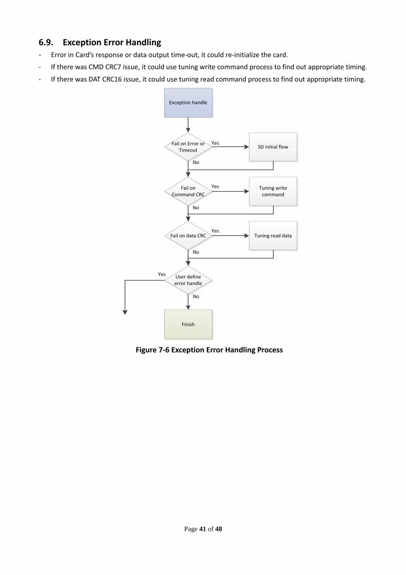
6.9. Exception Error Handling - Error in Card’s response or data output time-out, it could re-initialize the card.
- If there was CMD CRC7 issue, it could use tuning write command process to find out appropriate timing.
- If there was DAT CRC16 issue, it could use tuning read command process to find out appropriate timing.
Exception handle
Fail on Error orTimeout
Fail on Command CRC
SD initial flow
No
Yes
Tuning write command
Yes
No
Finish
User define error handle
Yes
No
Fail on data CRC Tuning read dataYes
No
Figure 7-6 Exception Error Handling Process

Page 42 of 48
6.10. Multiple Blocks Read (CMD18) Error Handling Process - If card responded ADDRESS_OUT_OF_Range, please check writing address
- If card responded DEVICE_IS_LOCKED, please stop writing data
- If card responded COM_CRC_ERROR, run Retry or Tuning Process
CMD18
CommandResponse
ResponseCRC7
Recovery
Retry
Read Data
Data CRC16
ReceivedEnd
CMD12
CMD13
CommandResponse
CommandResponse
Finish
Pass
Timeout
Not match
Pass
Yes
Pass
Transfer
ErrorTimeout
Recovery Tunning Write
Command
ErrorTimeout
Other state
Timeout
No
Yes
Recovery Tunning Read
Command
Not Match
No
Over SPEC timeout
No
Recovery Yes
Figure 7-7 Multiple Blocks Read (CMD18) Error Handling Process
Page 43 of 48
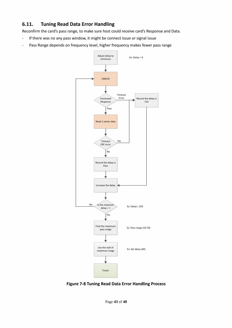
6.11. Tuning Read Data Error Handling Reconfirm the card’s pass range, to make sure host could receive card’s Response and Data.
- If there was no any pass window, it might be connect issue or signal issue
- Pass Range depends on frequency level, higher frequency makes fewer pass range
CMD19
CommandResponse
TimeoutError
Adjust delay to minimum
Record the delay is Fail
No Is the maxinum delay + 1
Yes
Record the delay is Pass
Increase the delay
Finish
Find the maximum pass range
Use the half of maximum range
Read 1 sector data
TimeoutCRC error
Yes
Pass
No
Ex: Pass range (10-70)
Ex: Set delay (40)
Ex: Delay = 0
Ex: Delay = 255
Figure 7-8 Tuning Read Data Error Handling Process

Page 44 of 48
Page 45 of 48
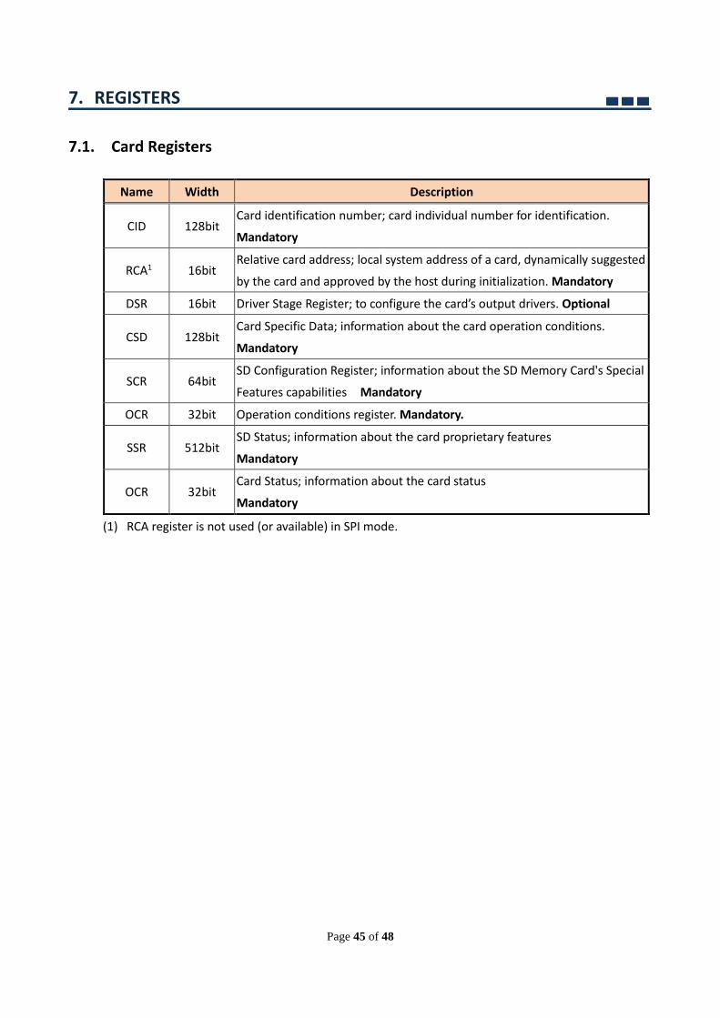
7. REGISTERS
7.1. Card Registers
Name Width Description
CID 128bit Card identification number; card individual number for identification.
Mandatory
RCA1 16bit Relative card address; local system address of a card, dynamically suggested
by the card and approved by the host during initialization. Mandatory
DSR 16bit Driver Stage Register; to configure the card’s output drivers. Optional
CSD 128bit Card Specific Data; information about the card operation conditions.
Mandatory
SCR 64bit SD Configuration Register; information about the SD Memory Card's Special
Features capabilities Mandatory
OCR 32bit Operation conditions register. Mandatory.
SSR 512bit SD Status; information about the card proprietary features
Mandatory
OCR 32bit Card Status; information about the card status
Mandatory
(1) RCA register is not used (or available) in SPI mode.

Page 46 of 48
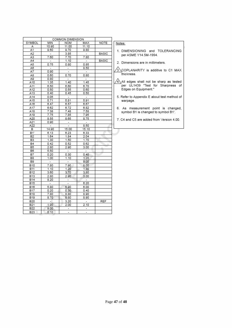
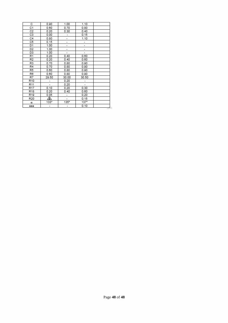
8. PHYSICAL DIMENSION
Dimension: 15mm(L) x 11mm(W) x 1mm(H)
Page 47 of 48
Page 48 of 48