instructions reference manual - assets.omron.com · cp1e cpu unit instructions reference...
TRANSCRIPT

INSTRUCTIONS
REFERENCE MANUAL
Cat. No. W483-E1-06
SYSMAC CP Series
CP1E-E@@SD@-@
CP1E-N@@S@D@-@
CP1E-E@@D@-@
CP1E-N@@D@-@
CP1E-NA@@D@-@
CP1E CPU Unit

© OMRON, 2009All rights reserved. No part of this publication may be reproduced, stored in a retrieval system, or transmitted, in any form, orby any means, mechanical, electronic, photocopying, recording, or otherwise, without the prior written permission ofOMRON.
No patent liability is assumed with respect to the use of the information contained herein. Moreover, because OMRON is con-stantly striving to improve its high-quality products, the information contained in this manual is subject to change withoutnotice. Every precaution has been taken in the preparation of this manual. Nevertheless, OMRON assumes no responsibilityfor errors or omissions. Neither is any liability assumed for damages resulting from the use of the information contained inthis publication.


SYSMAC CP SeriesCP1E-E@@SD@-@CP1E-N@@S@D@-@CP1E-E@@D@-@CP1E-N@@D@-@CP1E-NA@@D@-@CP1E CPU UnitInstructions Reference ManualRevised November 2014

Introduction
Thank you for purchasing a SYSMAC CP-series CP1E Programmable Controller.
This manual contains information required to use the CP1E. Read this manual completely and be sureyou understand the contents before attempting to use the CP1E.
This manual is intended for the following personnel, who must also have knowledge of electrical sys-tems (an electrical engineer or the equivalent).
• Personnel in charge of installing FA systems
• Personnel in charge of designing FA systems
• Personnel in charge of managing FA systems and facilities
CP-series CP1E CPU Units• Basic Models CP1E-E(S)D-
A basic model of CPU Unit that support basic control applications using instructions such asbasic, movement, arithmetic, and comparison instructions.
• Application Models CP1E-N/NA(S)D-An application model of CPU Unit that supports connections to Programmable Terminals, invert-ers, and servo drives.
The CP Series is centered around the CP1H, CP1L, and CP1E CPU Units and is designed with thesame basic architecture as the CS and CJ Series.
Always use CP-series Expansion Units and CP-series Expansion I/O Units when expanding I/Ocapacity. I/O words are allocated in the same way as for the CPM1A/CPM2A PLCs, i.e., using fixedareas for inputs and outputs.
Intended Audience
Applicable Products
1CP1E CPU Unit Instructions Reference Manual(W483)

CP1E CPU Unit Manuals
Information on the CP1E CPU Units is provided in the following manuals.
Refer to the appropriate manual for the information that is required.
This Manual
Mounting and Setting Hardware1
2
3
4
5
6
7
Wiring
Connecting Online to the PLC
Software Setup
Creating the Program
Checking and Debugging Operation
Maintenance and Troubleshooting
CP1E CPU Unit Hardware User’s Manual(Cat. No. W479)
CP1E CPU Unit Software User’s Manual(Cat. No. W480)
· Wiring methods for the power supply· Wiring methods between external I/O devices and Expansion I/O Units or Expansion Units
Connecting Cables for CX-Programmer Support Software
Error codes and remedies if a problem occurs
Procedures for connecting the CX-Programmer Support Software
Software setting methods for the CPU Units (PLC Setup)
· Checking I/O wiring, setting the Auxiliary Area settings, and performing trial operation
· Monitoring and debugging with the CX-Programmer
· Program types and basic information· CPU Unit operation· Internal memory· Built-in CPU functions· Settings
· Names and specifications of the parts of all Units· Basic system configuration for each CPU Unit· Connection methods for Expansion I/O Units and Expansion Units
CP1E CPU Unit Instructions Reference Manual(Cat. No. W483)
Detailed information on programming instructions
2 CP1E CPU Unit Instructions Reference Manual(W483)

The CP1E CPU manuals are organized in the sections listed in the following tables. Refer to the appro-priate section in the manuals as required.
Manual Configuration
CP1E CPU Unit Instructions Reference Manual (Cat. No. W483)(This Manual)
Section Contents
Section 1 Summary of Instructions This section provides a summary of instructions used with a CP1E CPU Unit.
Section 2 Instruction This section describes the functions, operands and sample programs of the instructions that are supported by a CP1E CPU Unit.
Section 3 Instruction Execution Times and Number of Steps
This section provides the execution times for all instructions used with a CP1E CPU Unit.
Section 4 Monitoring and Computing the Cycle Time
This section describes how to monitor and calculate the cycle time of a CP1E CPU Unit that can be used in the programs.
Appendices The appendices provide a list of instructions by Mnemonic and ASCII code table for the CP1E CPU Unit.
CP1E CPU Unit Software User’s Manual (Cat. No. W480)
Section Contents
Section 1 Overview This section gives an overview of the CP1E, describes its application procedures.
Section 2 CPU Unit Memory This section describes the types of internal memory in a CP1E CPU Unit and the data that is stored.
Section 3 CPU Unit Operation This section describes the operation of a CP1E CPU Unit.
Section 4 Programming Concepts This section provides basic information on designing ladder programs for a CP1E CPU Unit.
Section 5 I/O Memory This section describes the types of I/O memory areas in a CP1E CPU Unit and the details.
Section 6 I/O Allocation This section describes I/O allocation used to exchange data between the CP1E CPU Unit and other units.
Section 7 PLC Setup This section describes the PLC Setup, which are used to perform basic settings for a CP1E CPU Unit.
Section 8 Overview and Allocation of Built-in Functions
This section lists the built-in functions and describes the overall applica-tion flow and the allocation of the functions.
Section 9 Quick-response Inputs This section describes the quick-response inputs that can be used to read signals that are shorter than the cycle time.
Section 10 Interrupts This section describes the interrupts that can be used with CP1E PLCs, including input interrupts and scheduled interrupts.
Section 11 High-speed Counters This section describes the high-speed counter inputs, high-speed counter interrupts, and the frequency measurement function.
Section 12 Pulse Outputs This section describes positioning functions such as trapezoidal control, jogging, and origin searches.
Section 13 PWM Outputs This section describes the variable-duty-factor pulse (PWM) outputs.
Section 14 Serial Communications This section describes communications with Programmable Terminals (PTs) without using communications programming, no-protocol commu-nications with general components, and connections with a Modbus-RTU Easy Master, Serial PLC Link, and host computer.
3CP1E CPU Unit Instructions Reference Manual(W483)

Section 15 Analog I/O Function This section describes the built-in analog function for NA-type CPU Units.
Section 16 Built-in Functions This section describes PID temperature control, clock functions, DM backup functions, security functions.
Section 17 Ethernet Option Board This section gives an overview of the Ethernet Option Board, describes its setting methods, I/O memory allocations, troubleshooting, how to connect the CX-Programmer, and how to install an Ethernet network.
Section 18 Operating the Program-ming Device
This section describes basic functions of the CX-Programmer, such as using the CX-Programmer to write ladder programs to control the CP1E CPU Unit, to transfer the programs to the CP1E CPU Unit, and to debug the programs.
Appendices The appendices provide lists of programming instructions, the Auxiliary Area, cycle time response performance, PLC performance at power interruptions.
CP1E CPU Unit Hardware User’s Manual (Cat. No. W479)
Section Contents
Section 1 Overview and Specifica-tions
This section gives an overview of the CP1E, describes its features, and provides its specifications.
Section 2 Basic System Configura-tion and Devices
This section describes the basic system configuration and unit models of the CP1E.
Section 3 Part Names and Functions This section describes the part names and functions of the CPU Unit, Expansion I/O Units, and Expansion Units in a CP1E PLC .
Section 4 Programming Device This section describes the features of the CX-Programmer used for pro-gramming and debugging PLCs, as well as how to connect the PLC with the Programming Device by USB.
Section 5 Installation and Wiring This section describes how to install and wire CP1E Units.
Section 6 Troubleshooting This section describes how to troubleshoot problems that may occur with a CP1E PLC, including the error indications provided by the CP1E Units.
Section 7 Maintenance and Inspec-tion
This section describes periodic inspections, the service life of the Bat-tery, and how to replace the Battery.
Section 8 Using Expansion Units and Expansion I/O Units
This section describes application methods for Expansion Units.
Appendices The appendices provide information on dimensions, wiring diagrams, and wiring serial communications for the CP1E.
Section Contents
4 CP1E CPU Unit Instructions Reference Manual(W483)
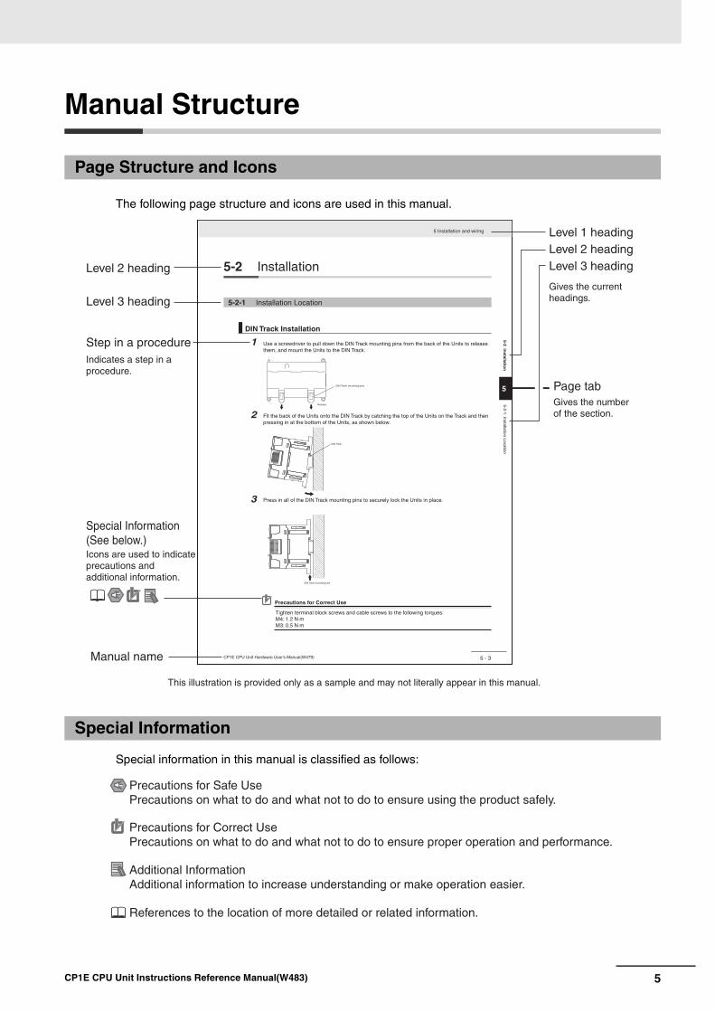
Manual Structure
The following page structure and icons are used in this manual.
Special information in this manual is classified as follows:
Page Structure and Icons
Special Information
5 - 3
5 Installation and wiring
CP1E CPU Unit Hardware User’s Manual(W479)
5
5-2 Installation
5-2-1 Installation Location
DIN Track Installation
1
2Release
DIN Track mounting pins
3
DIN Track
DIN Track mounting pins
Precautions for Correct Use
Tighten terminal block screws and cable screws to the following torques.M4: 1.2 N·mM3: 0.5 N·m
Use a screwdriver to pull down the DIN Track mounting pins from the back of the Units to release them, and mount the Units to the DIN Track.
Fit the back of the Units onto the DIN Track by catching the top of the Units on the Track and then pressing in at the bottom of the Units, as shown below.
Press in all of the DIN Track mounting pins to securely lock the Units in place.
5-2 Installatio
n5-2-1 Installation Location
Level 1 headingLevel 2 headingLevel 3 headingLevel 2 heading
Step in a procedure
Manual name
Special Information (See below.)
Level 3 heading
Page tab
Gives the current headings.
Indicates a step in a procedure.
Gives the number of the section.
This illustration is provided only as a sample and may not literally appear in this manual.
Icons are used to indicate precautions and additional information.
Precautions for Safe UsePrecautions on what to do and what not to do to ensure using the product safely.
Precautions for Correct UsePrecautions on what to do and what not to do to ensure proper operation and performance.
Additional InformationAdditional information to increase understanding or make operation easier.
References to the location of more detailed or related information.
5CP1E CPU Unit Instructions Reference Manual(W483)

Terminology and Notation
Term Description
E-type CPU Unit A basic model of CPU Unit that support basic control applications using instructions such as basic, movement, arithmetic, and comparison instructions.
Basic models of CPU Units are called “E(S)-type CPU Units” in this manual.
The models of E(S)-type CPU Units are shown below.
CP1E-ED-
CP1E-ESD-
N-type CPU Unit An application model of CPU Unit that supports connections to Programmable Terminals, inverters, and servo drives.
Application models of CPU Units are called “N(S)-type CPU Units” in this manual.
The models of N(S)-type CPU Units are shown below.
CP1E-ND-
CP1E-NSD-
CP1E-NS1D-
NA-type CPU Unit An application model of CPU Unit that supports built-in analog and connections to Pro-grammable Terminals, inverters, and servo drives.
Application models of CPU Units with built-in analog are called “NA-type CPU Units” in this manual.
CX-Programmer A programming device that applies for programming and debugging PLCs.
The CX-Programmer includes the Micro PLC Edition CX-Programmer (CX-One Lite), the CX-Programmer (CX-One) and the CX-Programmer for CP1E.
This manual describes the unique applications and functions of the Micro PLC Edition CX-Programmer version 9.03 or higher CX-Programmer for CP1E.
“CX-Programmer” refers to the Micro PLC Edition CX-Programmer version 9.03 or higher CX-Programmer for CP1E in this manual.
Note E20/30/40(S) and N20/30/40(S) CPU Units are supported by CX-Programmer ver-sion 8.2 or higher. E10/14(S), N14/60(S) and NA20 CPU Units are supported by CX-Programmer version 9.03 or higher.E60S CPU Units are supported by CX-Pro-grammer version 9.42 or higher.
6 CP1E CPU Unit Instructions Reference Manual(W483)

1
2
3
4
A
Sections in this Manual
1
2
3
4
Summary of Instructions
A Appendices
Instructions
Instruction Execution Times and Number of Steps
Monitoring and Computing the Cycle Time
7CP1E CPU Unit Instructions Reference Manual(W483)
CONTENTS
Introduction ...............................................................................................................1
CP1E CPU Unit Manuals ...........................................................................................2
Manual Structure .......................................................................................................5
Terms and Conditions Agreement.........................................................................12
Safety Precautions..................................................................................................14
Precautions for Safe Use........................................................................................17
Regulations and Standards ...............................................................................18
Related Manuals ......................................................................................................19
Section 1 Summary of Instructions .............................................. 1-1
1-1 Summary of Instructions ........................................................................................................ 1-2
Section 2 Instructions .................................................................... 2-1
Notation and Layout of Instruction Descriptions ......................................................................... 2-2
Sequence Input Instructions .......................................................................................................... 2-5LD/LD NOT ................................................................................................................................................ 2-7AND/AND NOT .......................................................................................................................................... 2-9OR/OR NOT ............................................................................................................................................. 2-11AND LD/OR LD ........................................................................................................................................ 2-13NOT .......................................................................................................................................................... 2-16UP/DOWN ................................................................................................................................................ 2-17
Sequence Output Instructions ..................................................................................................... 2-18OUT/OUT NOT ........................................................................................................................................ 2-18TR ............................................................................................................................................................ 2-20KEEP ....................................................................................................................................................... 2-21DIFU ......................................................................................................................................................... 2-25DIFD ......................................................................................................................................................... 2-27SET/RSET ............................................................................................................................................... 2-29SETA/RSTA .............................................................................................................................................. 2-31SETB/RSTB ............................................................................................................................................. 2-33
Sequence Control Instructions..................................................................................................... 2-35END ......................................................................................................................................................... 2-38NOP ......................................................................................................................................................... 2-39IL/ILC ....................................................................................................................................................... 2-40MILH/MILR/MILC ..................................................................................................................................... 2-44JMP/CJP/JME .......................................................................................................................................... 2-53FOR/NEXT ............................................................................................................................................... 2-56BREAK ..................................................................................................................................................... 2-59
Timer and Counter Instructions ................................................................................................... 2-60TIM/TIMX ................................................................................................................................................. 2-66TIMH/TIMHX ............................................................................................................................................ 2-69TMHH/TMHHX ......................................................................................................................................... 2-72TTIM/TTIMX ............................................................................................................................................. 2-74TIML/TIMLX ............................................................................................................................................. 2-77
8 CP1E CPU Unit Instructions Reference Manual(W483)

CNT/CNTX .............................................................................................................................................. 2-80CNTR/CNTRX ......................................................................................................................................... 2-83CNR/CNRX .............................................................................................................................................. 2-86
Comparison Instructions .............................................................................................................. 2-88=, <>, <, <=, >, >= .................................................................................................................................... 2-88=DT, <>DT, <DT, <=DT, >DT, >=DT ......................................................................................................... 2-91CMP/CMPL .............................................................................................................................................. 2-95CPS/CPSL ............................................................................................................................................... 2-98TCMP .................................................................................................................................................... 2-101BCMP .................................................................................................................................................... 2-103ZCP/ZCPL ............................................................................................................................................. 2-105
Data Movement Instructions....................................................................................................... 2-108MOV/MOVL/MVN ................................................................................................................................... 2-108MOVB .................................................................................................................................................... 2-111MOVD .................................................................................................................................................... 2-113XFRB ..................................................................................................................................................... 2-115XFER ..................................................................................................................................................... 2-117BSET ..................................................................................................................................................... 2-119XCHG .................................................................................................................................................... 2-121DIST ...................................................................................................................................................... 2-123COLL ..................................................................................................................................................... 2-125
Data Shift Instructions ................................................................................................................ 2-127SFT ........................................................................................................................................................ 2-127SFTR ..................................................................................................................................................... 2-129WSFT .................................................................................................................................................... 2-131ASL ........................................................................................................................................................ 2-133ASR ....................................................................................................................................................... 2-134ROL ....................................................................................................................................................... 2-135ROR ....................................................................................................................................................... 2-137SLD/SRD ............................................................................................................................................... 2-139NASL/NSLL ........................................................................................................................................... 2-141NASR/NSRL .......................................................................................................................................... 2-144
Increment/Decrement Instructions ............................................................................................ 2-147++/++L ................................................................................................................................................... 2-147--/--L ...................................................................................................................................................... 2-150++B/++BL .............................................................................................................................................. 2-153--B/--BL ................................................................................................................................................. 2-156
Symbol Math Instructions........................................................................................................... 2-158+/+L ....................................................................................................................................................... 2-158+C/+CL .................................................................................................................................................. 2-160+B/+BL ................................................................................................................................................... 2-162+BC/+BCL ............................................................................................................................................. 2-164–/–L ........................................................................................................................................................ 2-166–C/–CL .................................................................................................................................................. 2-170–B/–BL ................................................................................................................................................... 2-172–BC/–BCL .............................................................................................................................................. 2-175*/*L ......................................................................................................................................................... 2-177*B/*BL .................................................................................................................................................... 2-179/, /L ......................................................................................................................................................... 2-181/B, /BL .................................................................................................................................................... 2-183
Conversion Instructions.............................................................................................................. 2-185BIN/BINL ................................................................................................................................................ 2-185BCD/BCDL ............................................................................................................................................ 2-187NEG ....................................................................................................................................................... 2-189MLPX ..................................................................................................................................................... 2-191DMPX .................................................................................................................................................... 2-196ASC ....................................................................................................................................................... 2-201HEX ....................................................................................................................................................... 2-205
Logic Instructions........................................................................................................................ 2-210ANDW/ANDL ......................................................................................................................................... 2-210ORW/ORWL .......................................................................................................................................... 2-212
9CP1E CPU Unit Instructions Reference Manual(W483)

XORW/XORL ......................................................................................................................................... 2-214COM/COML ........................................................................................................................................... 2-216
Special Math Instructions ........................................................................................................... 2-218APR ........................................................................................................................................................ 2-218BCNT ..................................................................................................................................................... 2-227
Floating-point Math Instructions................................................................................................ 2-229FIX/FIXL ................................................................................................................................................. 2-233FLT/FLTL ................................................................................................................................................ 2-235+F, –F, *F, /F ........................................................................................................................................... 2-237=F, <>F, <F, <=F, >F, >=F ........................................................................................................................ 2-241FSTR ...................................................................................................................................................... 2-244FVAL ...................................................................................................................................................... 2-249
Table Data Processing Instructions ........................................................................................... 2-253SWAP ..................................................................................................................................................... 2-253FCS ........................................................................................................................................................ 2-255
Data Control Instructions............................................................................................................ 2-257PIDAT ..................................................................................................................................................... 2-257TPO ........................................................................................................................................................ 2-269SCL ........................................................................................................................................................ 2-276SCL2 ...................................................................................................................................................... 2-280SCL3 ...................................................................................................................................................... 2-284AVG ........................................................................................................................................................ 2-287
Subroutines Instructions ............................................................................................................ 2-290SBS ........................................................................................................................................................ 2-290SBN/RET ............................................................................................................................................... 2-295
Interrupt Control Instructions..................................................................................................... 2-298MSKS ..................................................................................................................................................... 2-300CLI ......................................................................................................................................................... 2-303DI ........................................................................................................................................................... 2-306EI ............................................................................................................................................................ 2-307
High-speed Counter/Pulse Output Instructions........................................................................ 2-308INI .......................................................................................................................................................... 2-308PRV ........................................................................................................................................................ 2-311CTBL ...................................................................................................................................................... 2-315SPED ..................................................................................................................................................... 2-319PULS ...................................................................................................................................................... 2-323PLS2 ...................................................................................................................................................... 2-325ACC ....................................................................................................................................................... 2-331ORG ....................................................................................................................................................... 2-336PWM ...................................................................................................................................................... 2-339
Step Instructions ......................................................................................................................... 2-341SNXT/STEP ........................................................................................................................................... 2-342
Basic I/O Unit Instructions.......................................................................................................... 2-352IORF ...................................................................................................................................................... 2-352SDEC ..................................................................................................................................................... 2-354DSW ....................................................................................................................................................... 2-357MTR ....................................................................................................................................................... 2-3617SEG ..................................................................................................................................................... 2-365
Serial Communication Instructions ........................................................................................... 2-369TXD ........................................................................................................................................................ 2-369RXD ....................................................................................................................................................... 2-374
Clock Instructions........................................................................................................................ 2-380CADD/CSUB .......................................................................................................................................... 2-380DATE ...................................................................................................................................................... 2-385
Failure Diagnosis Instructions ................................................................................................... 2-387FAL ......................................................................................................................................................... 2-387FALS ...................................................................................................................................................... 2-393
10 CP1E CPU Unit Instructions Reference Manual(W483)
Other Instructions........................................................................................................................ 2-398STC/CLC ............................................................................................................................................... 2-398WDT ...................................................................................................................................................... 2-399
Section 3 Instruction Execution Times and Number of Steps ... 3-1
3-1 CP1E CPU Unit Instruction Execution Times and Number of Steps .................................. 3-2
Section 4 Monitoring and Computing the Cycle Time................. 4-1
4-1 Monitoring the Cycle Time...................................................................................................... 4-24-1-1 Monitoring the Cycle Time.......................................................................................................... 4-2
4-2 Computing the Cycle Time ..................................................................................................... 4-34-2-1 CPU Unit Operation Flowchart ................................................................................................... 4-34-2-2 Cycle Time Overview.................................................................................................................. 4-44-2-3 I/O Refresh Times for PLC Units ................................................................................................ 4-54-2-4 Cycle Time Calculation Example ................................................................................................ 4-64-2-5 Increase in Cycle Time for Online Editing................................................................................... 4-6
Section A Appendices ....................................................................A-1
Alphabetical List of Instructions by Mnemonic ....................................................................A-2
Revision History................................................................................ Revision-1
11CP1E CPU Unit Instructions Reference Manual(W483)
Terms and Conditions Agreement
Exclusive WarrantyOmron’s exclusive warranty is that the Products will be free from defects in materials and workman-ship for a period of twelve months from the date of sale by Omron (or such other period expressed in writing by Omron). Omron disclaims all other warranties, express or implied.
LimitationsOMRON MAKES NO WARRANTY OR REPRESENTATION, EXPRESS OR IMPLIED, ABOUT NON-INFRINGEMENT, MERCHANTABILITY OR FITNESS FOR A PARTICULAR PURPOSE OF THE PRODUCTS. BUYER ACKNOWLEDGES THAT IT ALONE HAS DETERMINED THAT THE PRODUCTS WILL SUITABLY MEET THE REQUIREMENTS OF THEIR INTENDED USE.
Omron further disclaims all warranties and responsibility of any type for claims or expenses based on infringement by the Products or otherwise of any intellectual property right.
Buyer RemedyOmron’s sole obligation hereunder shall be, at Omron’s election, to (i) replace (in the form originally shipped with Buyer responsible for labor charges for removal or replacement thereof) the non-com-plying Product, (ii) repair the non-complying Product, or (iii) repay or credit Buyer an amount equal to the purchase price of the non-complying Product; provided that in no event shall Omron be responsible for warranty, repair, indemnity or any other claims or expenses regarding the Products unless Omron’s analysis confirms that the Products were properly handled, stored, installed and maintained and not subject to contamination, abuse, misuse or inappropriate modification. Return of any Products by Buyer must be approved in writing by Omron before shipment. Omron Companies shall not be liable for the suitability or unsuitability or the results from the use of Products in combi-nation with any electrical or electronic components, circuits, system assemblies or any other materi-als or substances or environments. Any advice, recommendations or information given orally or in writing, are not to be construed as an amendment or addition to the above warranty.
See http://www.omron.com/global/ or contact your Omron representative for published information.
OMRON COMPANIES SHALL NOT BE LIABLE FOR SPECIAL, INDIRECT, INCIDENTAL, OR CON-SEQUENTIAL DAMAGES, LOSS OF PROFITS OR PRODUCTION OR COMMERCIAL LOSS IN ANY WAY CONNECTED WITH THE PRODUCTS, WHETHER SUCH CLAIM IS BASED IN CONTRACT, WARRANTY, NEGLIGENCE OR STRICT LIABILITY.
Further, in no event shall liability of Omron Companies exceed the individual price of the Product on which liability is asserted.
Warranty, Limitations of Liability
Warranties
Limitation on Liability; Etc
12 CP1E CPU Unit Instructions Reference Manual(W483)
Omron Companies shall not be responsible for conformity with any standards, codes or regulations which apply to the combination of the Product in the Buyer’s application or use of the Product. At Buyer’s request, Omron will provide applicable third party certification documents identifying ratings and limitations of use which apply to the Product. This information by itself is not sufficient for a com-plete determination of the suitability of the Product in combination with the end product, machine, sys-tem, or other application or use. Buyer shall be solely responsible for determining appropriateness of the particular Product with respect to Buyer’s application, product or system. Buyer shall take applica-tion responsibility in all cases.
NEVER USE THE PRODUCT FOR AN APPLICATION INVOLVING SERIOUS RISK TO LIFE OR PROPERTY WITHOUT ENSURING THAT THE SYSTEM AS A WHOLE HAS BEEN DESIGNED TO ADDRESS THE RISKS, AND THAT THE OMRON PRODUCT(S) IS PROPERLY RATED AND INSTALLED FOR THE INTENDED USE WITHIN THE OVERALL EQUIPMENT OR SYSTEM.
Omron Companies shall not be responsible for the user’s programming of a programmable Product, or any consequence thereof.
Data presented in Omron Company websites, catalogs and other materials is provided as a guide for the user in determining suitability and does not constitute a warranty. It may represent the result of Omron’s test conditions, and the user must correlate it to actual application requirements. Actual perfor-mance is subject to the Omron’s Warranty and Limitations of Liability.
Product specifications and accessories may be changed at any time based on improvements and other reasons. It is our practice to change part numbers when published ratings or features are changed, or when significant construction changes are made. However, some specifications of the Product may be changed without any notice. When in doubt, special part numbers may be assigned to fix or establish key specifications for your application. Please consult with your Omron’s representative at any time to confirm actual specifications of purchased Product.
Information presented by Omron Companies has been checked and is believed to be accurate; how-ever, no responsibility is assumed for clerical, typographical or proofreading errors or omissions.
Application Considerations
Suitability of Use
Programmable Products
Disclaimers
Performance Data
Change in Specifications
Errors and Omissions
13CP1E CPU Unit Instructions Reference Manual(W483)
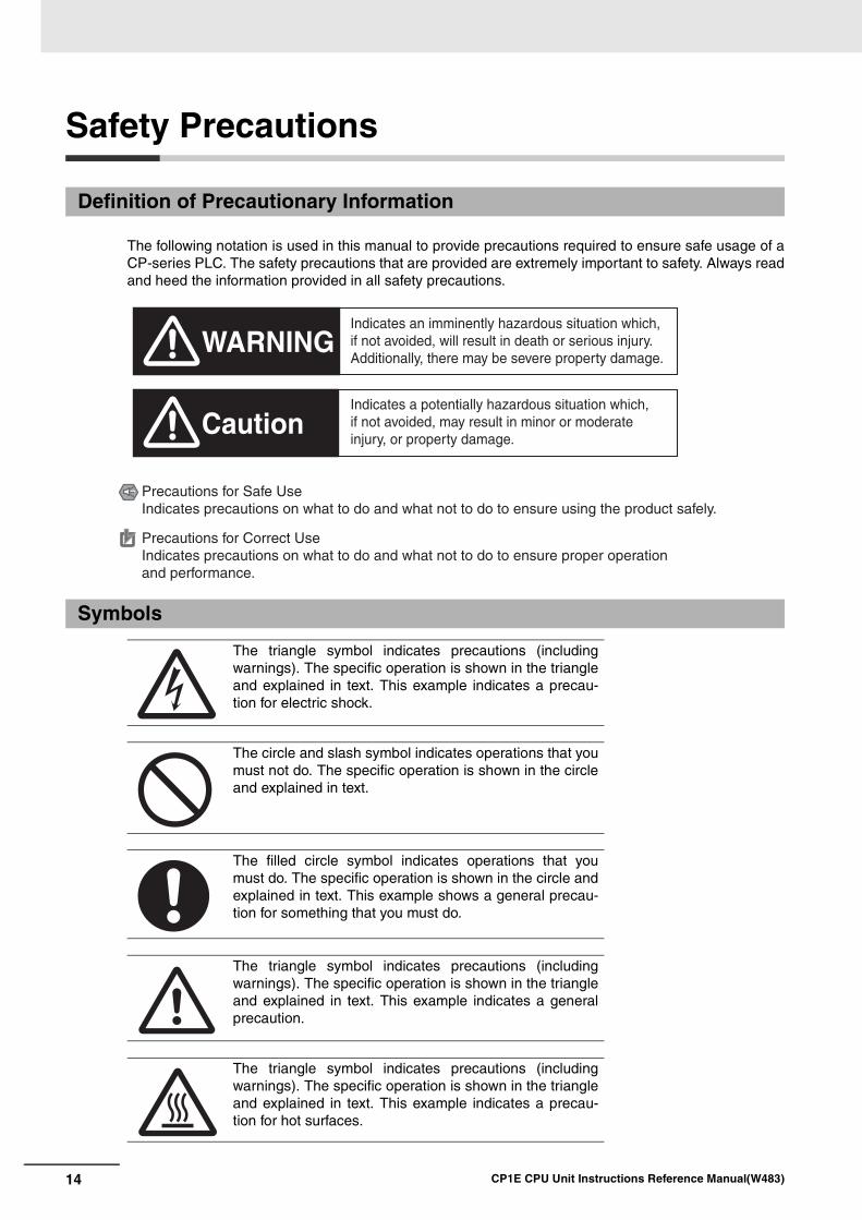
Safety Precautions
The following notation is used in this manual to provide precautions required to ensure safe usage of aCP-series PLC. The safety precautions that are provided are extremely important to safety. Always readand heed the information provided in all safety precautions.
Definition of Precautionary Information
Symbols
The triangle symbol indicates precautions (includingwarnings). The specific operation is shown in the triangleand explained in text. This example indicates a precau-tion for electric shock.
The circle and slash symbol indicates operations that youmust not do. The specific operation is shown in the circleand explained in text.
The filled circle symbol indicates operations that youmust do. The specific operation is shown in the circle andexplained in text. This example shows a general precau-tion for something that you must do.
The triangle symbol indicates precautions (includingwarnings). The specific operation is shown in the triangleand explained in text. This example indicates a generalprecaution.
The triangle symbol indicates precautions (includingwarnings). The specific operation is shown in the triangleand explained in text. This example indicates a precau-tion for hot surfaces.
WARNING
Caution
Indicates an imminently hazardous situation which, if not avoided, will result in death or serious injury. Additionally, there may be severe property damage.
Indicates a potentially hazardous situation which, if not avoided, may result in minor or moderate injury, or property damage.
Precautions for Safe UseIndicates precautions on what to do and what not to do to ensure using the product safely.
Precautions for Correct UseIndicates precautions on what to do and what not to do to ensure proper operation and performance.
14 CP1E CPU Unit Instructions Reference Manual(W483)

Be sure to sufficiently confirm the safety at the destination when you transfer the program or I/O memory or perform procedures to change the I/O memory.
Devices connected to PLC outputs may incorrectly operate regardless of the operat-ing mode of the CPU Unit.
With an E(S)-type CPU Unit or with an N/NA(S)-type CPU Unit without a Bat-tery, the contents of the DM Area (D) *, Holding Area (H), the Counter Present Values (C), the status of Counter Completion Flags (C), and the status of bits in the Auxiliary Area (A) related to clock functions may be unstable when the power supply is turned ON.
*This does not apply to areas backed up to EEPROM using the DM backup function.
If the DM backup function is being used, be sure to use one of the following methods for initialization.
1. Clearing All Areas to All Zeros
Select the Clear Held Memory (HR/DM/CNT) to Zero Check Box in the Startup Data Read Area in the PLC Setup.
2. Clearing Specific Areas to All Zeros or Initializing to Specific Values Make the settings from a ladder program.
If the data is not initialized, the unit or device may operate unexpectedly because of unstable data.
Execute online edit only after confirming that no adverse effects will be caused by extending the cycle time.
Otherwise, the input signals may not be readable.
The DM Area (D), Holding Area (H), Counter Completion Flags (C), and Counter Present Values (C) will be held by the Battery if a Battery is mounted in a CP1E-N/NA(S)D- CPU Unit. When the battery voltage is low, however, I/O mem-ory areas that are held (including the DM, Holding, and Counter Areas) will be unsta-ble. The unit or device may operate unexpectedly because of unstable data.
Use the Battery Error Flag or other measures to stop outputs if external out-puts are performed from a ladder program based on the contents of the DM Area or other I/O memory areas.
Sufficiently check safety if I/O bit status or present values are monitored in the Ladder Section Pane or present values are monitored in the Watch Pane.
If bits are set, reset, force-set, or force-reset by inadvertently pressing a shortcut key, devices connected to PLC outputs may operate incorrectly regardless of the operat-ing mode.
CautionCaution
15CP1E CPU Unit Instructions Reference Manual(W483)

Program so that the memory area of the start address is not exceeded when using a word address or symbol for the offset.
For example, write the program so that processing is executed only when the indirect specification does not cause the final address to exceed the memory area by using an input comparison instruction or other instruction.
If an indirect specification causes the address to exceed the area of the start address, the system will access data in other area, and unexpected operation may occur.
Set the temperature range according to the type of temperature sensor con-nected to the Unit.
Temperature data will not be converted correctly if the temperature range does not match the sensor.
Do not set the temperature range to any values other than those for which tem-perature ranges are given in the following table.
An incorrect setting may cause operating errors.
Caution
16 CP1E CPU Unit Instructions Reference Manual(W483)
Precautions for Safe Use
Observe the following precautions when using a CP-series PLC.
Handling• To initialize the DM Area, back up the initial contents for the DM Area to backup memory using
one of the following methods.• Set the number of words of the DM Area to be backed up starting with D0 in the Number of
CH of DM for backup Box in the Startup Data Read Area. • Include programming to back up specified words in the DM Area to built-in EEPROM by turn-
ing ON A751.15 (DM Backup Save Start Bit).• Check the ladder program for proper execution before actually running it on the Unit. Not checking
the program may result in an unexpected operation.• The ladder program and parameter area data in the CP1E CPU Units are backed up in the built-in
EEPROM backup memory. The BKUP indicator will light on the front of the CPU Unit when thebackup operation is in progress. Do not turn OFF the power supply to the CPU Unit when theBKUP indicator is lit. The data will not be backed up if power is turned OFF and a memory errorwill occur the next time the power supply is turned ON.
• With a CP1E CPU Unit, data memory can be backed up to the built-in EEPROM backup memory.The BKUP indicator will light on the front of the CPU Unit when backup is in progress. Do not turnOFF the power supply to the CPU Unit when the BKUP indicator is lit. If the power is turned OFFduring a backup, the data will not be backed up and will not be transferred to the DM Area in RAMthe next time the power supply is turned ON.
• Before replacing the battery, supply power to the CPU Unit for at least 30 minutes and then com-plete battery replacement within 5 minutes. Memory data may be corrupted if this precaution isnot observed.
• The equipment may operate unexpectedly if inappropriate parameters are set. Even if the appro-priate parameters are set, confirm that equipment will not be adversely affected before transfer-ring the parameters to the CPU Unit.
• Before starting operation, confirm that the contents of the DM Area is correct.• After replacing the CPU Unit, make sure that the required data for the DM Area, Holding Area, and
other memory areas has been transferred to the new CPU Unit before restarting operation.• Do not attempt to disassemble, repair, or modify any Units. Any attempt to do so may result in mal-
function, fire, or electric shock.• Confirm that no adverse effect will occur in the system before attempting any of the following. Not
doing so may result in an unexpected operation.• Changing the operating mode of the PLC (including the setting of the startup operating mode).• Force-setting/force-resetting any bit in memory.• Changing the present value of any word or any set value in memory.
External Circuits• Always configure the external circuits to turn ON power to the PLC before turning ON power to the
control system. If the PLC power supply is turned ON after the control power supply, temporaryerrors may result in control system signals because the output terminals on DC Output Units andother Units will momentarily turn ON when power is turned ON to the PLC.
• Fail-safe measures must be taken by the customer to ensure safety in the event that outputs fromoutput terminals remain ON as a result of internal circuit failures, which can occur in relays, tran-sistors, and other elements.
• If the I/O Hold Bit is turned ON, the outputs from the PLC will not be turned OFF and will maintaintheir previous status when the PLC is switched from RUN or MONITOR mode to PROGRAM mode.Make sure that the external loads will not produce dangerous conditions when this occurs. (Whenoperation stops for a fatal error, including those produced with the FALS instruction, all outputs fromPLC will be turned OFF and only the internal output status in the CPU Unit will be maintained.)
17CP1E CPU Unit Instructions Reference Manual(W483)

Regulations and Standards
SYSMAC is a registered trademark for Programmable Controllers made by OMRON Corporation.
CX-One is a registered trademark for Programming Software made by OMRON Corporation.
Windows is a registered trademark of Microsoft Corporation.
Other system names and product names in this document are the trademarks or registered trademarksof their respective companies.
Trademarks
18 CP1E CPU Unit Instructions Reference Manual(W483)

Related Manuals
The following manuals are related to the CP1E. Use them together with this manual.
Manual name Cat. No. Model numbers Application Contents
SYSMAC CP Series CP1E CPU Unit Instruc-tions Reference Manual (this manual)
W483 CP1E-ESD-
CP1E-NSD-
CP1E-ED-
CP1E-ND-
CP1E-NAD-
To learn program-ming instructions in detail
Describes each programming instruction in detail.
When programming, use this manual together with the CP1E CPU Unit Software User’s Man-ual (Cat. No. W480).
SYSMAC CP Series CP1E CPU Unit Soft-ware User’s Manual
W480 CP1E-ESD-
CP1E-NSD-
CP1E-ED-
CP1E-ND-
CP1E-NAD-
To learn the software specifications of the CP1E PLCs
Describes the following information for CP1E PLCs.
• CPU Unit operation
• Internal memory
• Programming
• Settings
• CPU Unit built-in functions
• Interrupts
• High-speed counter inputs
• Pulse outputs
• Serial communications
• Other functions
Use this manual together with the CP1E CPU Unit Hardware User’s Manual (Cat. No. W479) and Instructions Reference Manual (Cat. No. W483).
SYSMAC CP Series CP1E CPU Unit Hard-ware User’s Manual
W479 CP1E-ESD-
CP1E-NSD-
CP1E-ED-
CP1E-ND-
CP1E-NAD-
To learn the hard-ware specifications of the CP1E PLCs
Describes the following information for CP1E PLCs.
• Overview and features
• Basic system configuration
• Part names and functions
• Installation and settings
• Troubleshooting
Use this manual together with the CP1E CPU Unit Software User’s Manual (Cat. No. W480) and Instructions Reference Manual (Cat. No. W483).
CS/CJ/CP/NSJ Series Communications Com-mands Reference Man-ual
W342 CS1G/H-CPUH
CS1G/H-CPU-V1
CS1D-CPUH
CS1D-CPUS
CS1W-SCU-V1
CS1W-SCB-V1
CJ1G/H-CPUH
CJ1G-CPUP
CJ1M-CPU
CJ1G-CPU
CJ1W-SCU-V1
To learn communica-tions commands for CS/CJ/CP/NSJ-series Controllers in detail
Describes
1) C-mode commands and2) FINS commands in detail.
Read this manual for details on C-mode and FINS commands addressed to CPU Units.
Note This manual describes commands addressed to CPU Units. Itdoes not cover commands addressed to other Units or ports (e.g.,serial communications ports on CPU Units, communications portson Serial Communications Units/Boards, and other Communica-tions Units).
SYSMAC CP Series
CP1L/CP1E CPU Unit
Introduction Manual
W461 CP1L-L10D-
CP1L-L14D-
CP1L-L20D-
CP1L-M30D-
CP1L-M40D-
CP1L-M60D-
CP1E-ED-
CP1E-ND-
CP1E-NAD-
To learn the basic setup methods of the CP1L/CP1E PLCs
Describes the following information for CP1L/CP1E PLCs.
• Basic configuration and component names
• Mounting and wiring
• Programming, data transfer, and debugging using the CX-Programmer
• Application program examples
CX-Simulator Operation
Manual
W366 CXONE-ALC-V4/ALD-V4
Operating procedures for CX-Simulator Simulation Support Software for Windows computersUsing simulation in the CX-Programmer with CX-Programmer
Describes the operating procedures for the
CX-Simulator.
19CP1E CPU Unit Instructions Reference Manual(W483)

20 CP1E CPU Unit Instructions Reference Manual(W483)
11
This section provides a summary of instructions used with a CP1E CPU Unit.
1-1 Summary of Instructions . . . . . . . . . . . . . . . . . . . . . . . . . . . . . . . . . . . . . . . . 1-2
Summary of Instructions
1-1CP1E CPU Unit Instructions Reference Manual(W483)

1 Summary of Instructions
1-1 Summary of Instructions
There are 200 types of instructions can be used by CP1E.The following table lists the instructions by function. Refer to the reference pages for the
detail of each instruction.
Instrucion Type
Instruction MnemonicFUNNo.
Function Page
Sequence Input Instruc-tions
LOAD LD - Indicates a logical start and creates an ON/OFF execution condition based on the ON/OFF status of the specified operand bit.
2-7
@LD -
%LD -
!LD -
!@LD -
!%LD -
LOAD NOT LD NOT - Indicates a logical start and creates an ON/OFF execution condition based on the reverse of the ON/OFF status of the specified operand bit.
2-7
@LD NOT -
%LD NOT -
!LD NOT -
!@LD NOT -
!%LD NOT -
AND AND - Takes a logical AND of the status of the specified operand bit and the current execution condition.
2-9
@AND -
%AND -
!AND -
!@AND -
!%AND -
AND NOT AND NOT - Reverses the status of the specified operand bit and takes a logical AND with the current execution condition.
2-9
@AND NOT -
%AND NOT -
!AND NOT -
!@AND NOT -
!%AND NOT -
OR OR - Takes a logical OR of the ON/OFF status of the specified operand bit and the current execution condition.
2-11
@OR -
%OR -
!OR -
!@OR -
!%OR -
OR NOT OR NOT - Reverses the status of the specified bit and takes a logical OR with the current execution condition.
2-11
@OR NOT -
%OR NOT -
!OR NOT -
!@OR NOT -
!%OR NOT -
AND LOAD AND LD - Takes a logical AND between logic blocks. 2-13
OR LOAD OR LD - Takes a logical OR between logic blocks. 2-13
NOT NOT 520 Reverses the execution condition. 2-16
CONDITION ON UP 521 UP(521) turns ON the execution condition for one cycle when the execution condition goes from OFF to ON.
2-17
CONDITION OFF DOWN 522 DOWN(522) turns ON the execution condition for one cycle when the execution condition goes from ON to OFF.
2-17
1-2 CP1E CPU Unit Instructions Reference Manual(W483)

1 Summary of Instructions1-1 S
um
mary o
f Instru
ction
s
1
Sequence Output Instructions
OUTPUT OUT - Outputs the result (execution condition) of the logical processing to the speci-fied bit.
2-18
!OUT -
OUTPUT NOT OUT NOT - Reverses the result (execution condition) of the logical processing, and outputs it to the specified bit.
2-18
!OUT NOT -
TR Bits TR - TR bits are used to temporarily retain the ON/OFF status of execution condi-tions in a program when programming in mnemonic code.
2-20
KEEP KEEP 011 Operates as a latching relay. 2-21
!KEEP
DIFFERENTIATEUP
DIFU 013 DIFU(013) turns the designated bit ON for one cycle when the execution condi-tion goes from OFF to ON (rising edge).
2-25
!DIFU
DIFFERENTIATEDOWN
DIFD 014 DIFD(014) turns the designated bit ON for one cycle when the execution condi-tion goes from ON to OFF (falling edge).
2-27
!DIFD
SET SET - SET turns the operand bit ON when the execution condition is ON. 2-29
@SET -
%SET -
!SET -
!@SET -
!%SET -
RESET RSET - RSET turns the operand bit OFF when the execution condition is ON. 2-29
@RSET -
%RSET -
!RSET -
!@RSET -
!%RSET -
MULTIPLE BIT SET SETA 530 SETA(530) turns ON the specified number of consecutive bits. 2-31
@SETA
MULTIPLE BIT RESET
RSTA 531 RSTA(531) turns OFF the specified number of consecutive bits. 2-31
@RSTA
SINGLE BIT SET SETB 532 SETB(532) turns ON the specified bit in the specified word when the execution condition is ON.
Unlike the SET instruction, SETB(532) can be used to set a bit in a DM word.
2-33
@SETB
!SETB
!@SETB
SINGLE BIT RESET RSTB 533 RSTB(533) turns OFF the specified bit in the specified word when the execu-tion condition is ON.
Unlike the RSET instruction, RSTB(533) can be used to reset a bit in a DM word.
2-33
@RSTB
!RSTB
!@RSTB
Instrucion Type
Instruction MnemonicFUNNo.
Function Page
1-3CP1E CPU Unit Instructions Reference Manual(W483)

1 Summary of Instructions
Sequence Control Instructions
END END 001 Indicates the end of a program. 2-38
NO OPERATION NOP 000 This instruction has no function. (No processing is performed for NOP(000).) 2-39
INTERLOCK IL 002 Interlocks all outputs between IL(002) and ILC(003) when the execution condi-tion for IL(002) is OFF.
2-40
INTERLOCK CLEAR
ILC 003 All outputs between IL(002) and ILC(003) are interlocked when the execution condition for IL(002) is OFF.
2-40
MULTI-INTERLOCKDIFFERENTIATIONHOLD
MILH 517 When the execution condition for MILH(517) is OFF, the outputs for all instruc-tions between that MILH(517) instruction and the next MILC(519) instruction are interlocked.
2-44
MULTI-INTERLOCKDIFFERENTIATIONRELEASE
MILR 518 When the execution condition for MILR(518) is OFF, the outputs for all instruc-tions between that MILR(518) instruction and the next MILC(519) instruction are interlocked.
2-44
MULTI-INTERLOCKCLEAR
MILC 519 Clears an interlock started by an MILH(517) or MILR(518) with the same inter-lock number.
2-44
JUMP JMP 004 When the execution condition for JMP(004) is OFF, program execution jumps directly to the first JME(005) in the program with the same jump number.
2-53
JUMP END JME 005 Indicates the end of a jump initiated by JMP(004) or CJP(510). 2-53
CONDITIONAL JUMP
CJP 510 The operation of CJP(510) is the basically the opposite of JMP(004). When the execution condition for CJP(510) is ON, program execution jumps directly to the first JME(005) in the program with the same jump number.
2-53
FOR LOOP FOR 512 The instructions between FOR(512) and NEXT(513) are repeated a specified number of times.
2-56
NEXT LOOP NEXT 513 The instructions between FOR(512) and NEXT(513) are repeated a specified number of times.
2-56
BREAK LOOP BREAK 514 Programmed in a FOR-NEXT loop to cancel the execution of the loop for a given execution condition. The remaining instructions in the loop are processed as NOP(000) instructions.
2-59
Timer and Counter Instructions
HUNDRED-MS TIMER
TIM - TIM/TIMX(550) operates a decrementing timer with units of 0.1-s. 2-66
TIMX 550
TEN-MS TIMER TIMH 015 TIMH(015)/TIMHX(551) operates a decrementing timer with units of 10-ms. 2-69
TIMHX 551
ONE-MS TIMER TMHH 540 TMHH(540)/TMHHX(552) operates a decrementing timer with units of 1-ms. 2-72
TMHHX 552
ACCUMULATIVE TIMER
TTIM 087 TTIM(087)/TTIMX(555) operates an incrementing timer with units of 0.1-s. 2-74
TTIMX 555
LONG TIMER TIML 542 TIML(542)/TIMLX(553) operates a decrementing timer with units of 0.1-s. 2-77
TIMLX 553
COUNTER CNT - CNT/CNTX(546) operates a decrementing counter. 2-80
CNTX 546
REVERSIBLE COUNTER
CNTR 012 CNTR(012)/CNTRX(548) operates a reversible counter. 2-83
CNTRX 548
RESET TIMER/ COUNTER
CNR/@CNR
545 CNR(545)/CNRX(547) resets the timers or counters within the specified range of timer or counter numbers.
2-86
CNRX/@CNRX
547
Instrucion Type
Instruction MnemonicFUNNo.
Function Page
1-4 CP1E CPU Unit Instructions Reference Manual(W483)
1 Summary of Instructions1-1 S
um
mary o
f Instru
ction
s
1
Comparison Instructions
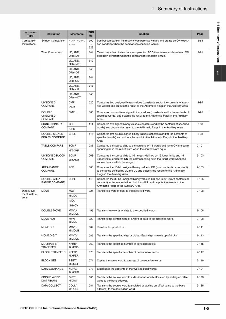
Symbol Comparison = , <> , < , <= , > , >=
300∼
328
Symbol comparison instructions compare two values and create an ON execu-tion condition when the comparison condition is true.
2-88
Time Comparison LD, AND, OR+=DT
341 Time comparison instructions compare two BCD time values and create an ON execution condition when the comparison condition is true.
2-91
LD, AND, OR+<>DT
342
LD, AND, OR+<DT
343
LD, AND, OR+<=DT
344
LD, AND, OR+>DT
345
LD, AND, OR+>=DT
346
UNSIGNED COMPARE
CMP 020 Compares two unsigned binary values (constants and/or the contents of speci-fied words) and outputs the result to the Arithmetic Flags in the Auxiliary Area.
2-95
!CMP
DOUBLE UNSIGNED COMPARE
CMPL 060 Compares two double unsigned binary values (constants and/or the contents of specified words) and outputs the result to the Arithmetic Flags in the Auxiliary Area.
2-95
SIGNED BINARY COMPARE
CPS 114 Compares two signed binary values (constants and/or the contents of specified words) and outputs the result to the Arithmetic Flags in the Auxiliary Area.
2-98
!CPS
DOUBLE SIGNED BINARY COMPARE
CPSL 115 Compares two double signed binary values (constants and/or the contents of specified words) and outputs the result to the Arithmetic Flags in the Auxiliary Area.
2-98
TABLE COMPARE TCMP 085 Compares the source data to the contents of 16 words and turns ON the corre-sponding bit in the result word when the contents are equal.
2-101
@TCMP
UNSIGNED BLOCK COMPARE
BCMP 068 Compares the source data to 16 ranges (defined by 16 lower limits and 16 upper limits) and turns ON the corresponding bit in the result word when the source data is within the range.
2-103
@BCMP
AREA RANGE COMPARE
ZCP 088 Compares the 16-bit unsigned binary value in CD (word contents or constant) to the range defined by LL and UL and outputs the results to the Arithmetic Flags in the Auxiliary Area.
2-105
DOUBLE AREA RANGE COMPARE
ZCPL 116 Compares the 32-bit unsigned binary value in CD and CD+1 (word contents or constant) to the range defined by LL and UL and outputs the results to the Arithmetic Flags in the Auxiliary Area.
2-105
Data Move-ment Instruc-tions
MOVE MOV 021 Transfers a word of data to the specified word. 2-108
@MOV
!MOV
!@MOV
DOUBLE MOVE MOVL/@MOVL
498 Transfers two words of data to the specified words. 2-108
MOVE NOT MVN/@MVN
022 Transfers the complement of a word of data to the specified word. 2-108
MOVE BIT MOVB/@MOVB
082 Transfers the specified bit. 2-111
MOVE DIGIT MOVD/@MOVD
083 Transfers the specified digit or digits. (Each digit is made up of 4 bits.) 2-113
MULTIPLE BIT TRANSFER
XFRB/@XFRB
062 Transfers the specified number of consecutive bits. 2-115
BLOCK TRANSFER XFER/@XFER
070 Transfers the specified number of consecutive words. 2-117
BLOCK SET BSET/@BSET
071 Copies the same word to a range of consecutive words. 2-119
DATA EXCHANGE XCHG/@XCHG
073 Exchanges the contents of the two specified words. 2-121
SINGLE WORD DISTRIBUTE
DIST/@DIST
080 Transfers the source word to a destination word calculated by adding an offset value to the base address.
2-123
DATA COLLECT COLL/@COLL
081 Transfers the source word (calculated by adding an offset value to the base address) to the destination word.
2-125
Instrucion Type
Instruction MnemonicFUNNo.
Function Page
1-5CP1E CPU Unit Instructions Reference Manual(W483)

1 Summary of Instructions
Data Shift Instructions
SHIFT REGISTER SFT 010 Operates a shift register. 2-127
REVERSIBLESHIFT REGISTER
SFTR/@SFTR
084 Creates a shift register that shifts data to either the right or the left. 2-129
WORD SHIFT WSFT/@WSFT
016 Shifts data between St and E in word units. 2-131
ARITHMETIC SHIFT LEFT
ASL/@ASL
025
Shifts the contents of Wd one bit to the left.2-133
ARITHMETIC SHIFT RIGHT
ASR/@ASR
026 Shifts the contents of Wd one bit to the right. 2-134
ROTATE LEFT ROL/@ROL
027 Shifts all Wd bits one bit to the left including the Carry Flag (CY). 2-135
ROTATE RIGHT ROR/@ROR
028 Shifts all Wd bits one bit to the right including the Carry Flag (CY). 2-137
ONE DIGIT SHIFT LEFT
SLD/@SLD
074 Shifts data by one digit (4 bits) to the left. 2-139
ONE DIGIT SHIFT RIGHT
SRD/@SRD
075 Shifts data by one digit (4 bits) to the right. 2-139
SHIFT N-BITS LEFT NASL/@NASL
580 Shifts the specified 16 bits of word data to the left by the specified number of bits.
2-141
DOUBLE SHIFT N-BITS LEFT
NSLL/@NSLL
582 Shifts the specified 32 bits of word data to the left by the specified number of bits.
2-141
SHIFT N-BITS RIGHT
NASR/@NASR
581 Shifts the specified 16 bits of word data to the right by the specified number of bits.
2-144
DOUBLE SHIFT N-BITS RIGHT
NSRL/@NSRL
583 Shifts the specified 32 bits of word data to the right by the specified number of bits.
2-144
Increment/Decrement Instructions
INCREMENT BINARY
++/@++
590 Increments the 4-digit hexadecimal content of the specified word by 1. 2-147
DOUBLE INCRE-MENT BINARY
++L/@++L
591 Increments the 8-digit hexadecimal content of the specified words by 1. 2-147
DECREMENT BINARY
--/@--
592 Decrements the 4-digit hexadecimal content of the specified word by 1. 2-150
DOUBLE DECRE-MENT BINARY
--L/@--L
593 Decrements the 8-digit hexadecimal content of the specified words by 1. 2-150
INCREMENT BCD ++B/@++B
594 Increments the 4-digit BCD content of the specified word by 1. 2-153
DOUBLE INCRE-MENT BCD
++BL/@++BL
595 Increments the 8-digit BCD content of the specified words by 1. 2-153
DECREMENT BCD --B/@--B
596 Decrements the 4-digit BCD content of the specified word by 1. 2-156
DOUBLE DECRE-MENT BCD
--BL/@--BL
597 Decrements the 8-digit BCD content of the specified words by 1. 2-156
Instrucion Type
Instruction MnemonicFUNNo.
Function Page
1-6 CP1E CPU Unit Instructions Reference Manual(W483)
1 Summary of Instructions1-1 S
um
mary o
f Instru
ction
s
1
Symbol Math Instructions
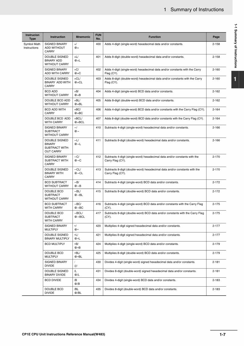
SIGNED BINARY ADD WITHOUT CARRY
+/@+
400 Adds 4-digit (single-word) hexadecimal data and/or constants. 2-158
DOUBLE SIGNED BINARY ADD WITHOUT CARRY
+L/@+L
401 Adds 8-digit (double-word) hexadecimal data and/or constants. 2-158
SIGNED BINARY ADD WITH CARRY
+C/@+C
402 Adds 4-digit (single-word) hexadecimal data and/or constants with the Carry Flag (CY).
2-160
DOUBLE SIGNED BINARY ADD WITH CARRY
+CL/@+CL
403 Adds 8-digit (double-word) hexadecimal data and/or constants with the Carry Flag (CY).
2-160
BCD ADD WITHOUT CARRY
+B/@+B
404 Adds 4-digit (single-word) BCD data and/or constants. 2-162
DOUBLE BCD ADD WITHOUT CARRY
+BL/@+BL
405 Adds 8-digit (double-word) BCD data and/or constants. 2-162
BCD ADD WITH CARRY
+BC/@+BC
406 Adds 4-digit (single-word) BCD data and/or constants with the Carry Flag (CY). 2-164
DOUBLE BCD ADD WITH CARRY
+BCL/@+BCL
407 Adds 8-digit (double-word) BCD data and/or constants with the Carry Flag (CY). 2-164
SIGNED BINARY SUBTRACT WITHOUT CARRY
-/@-
410 Subtracts 4-digit (single-word) hexadecimal data and/or constants. 2-166
DOUBLE SIGNED BINARY SUBTRACT WITH-OUT CARRY
-L/@-L
411 Subtracts 8-digit (double-word) hexadecimal data and/or constants. 2-166
SIGNED BINARY SUBTRACT WITH CARRY
-C/@-C
412 Subtracts 4-digit (single-word) hexadecimal data and/or constants with the Carry Flag (CY).
2-170
DOUBLE SIGNED BINARY WITH CARRY
-CL/@-CL
413 Subtracts 8-digit (double-word) hexadecimal data and/or constants with the Carry Flag (CY).
2-170
BCD SUBTRACT WITHOUT CARRY
-B/@-B
414 Subtracts 4-digit (single-word) BCD data and/or constants. 2-172
DOUBLE BCD SUBTRACT WITHOUT CARRY
-BL/@-BL
415 Subtracts 8-digit (double-word) BCD data and/or constants. 2-172
BCD SUBTRACT WITH CARRY
-BC/@-BC
416 Subtracts 4-digit (single-word) BCD data and/or constants with the Carry Flag (CY).
2-175
DOUBLE BCD SUBTRACT WITH CARRY
-BCL/@-BCL
417 Subtracts 8-digit (double-word) BCD data and/or constants with the Carry Flag (CY).
2-175
SIGNED BINARY MULTIPLY
∗/@∗
420 Multiplies 4-digit signed hexadecimal data and/or constants. 2-177
DOUBLE SIGNED BINARY MULTIPLY
∗L/@∗L
421 Multiplies 8-digit signed hexadecimal data and/or constants. 2-177
BCD MULTIPLY ∗B/@∗B
424 Multiplies 4-digit (single-word) BCD data and/or constants. 2-179
DOUBLE BCD MULTIPLY
∗BL/@∗BL
425 Multiplies 8-digit (double-word) BCD data and/or constants. 2-179
SIGNED BINARY DIVIDE
/
@/
430 Divides 4-digit (single-word) signed hexadecimal data and/or constants. 2-181
DOUBLE SIGNED BINARY DIVIDE
/L @/L
431 Divides 8-digit (double-word) signed hexadecimal data and/or constants. 2-181
BCD DIVIDE /B @/B
434 Divides 4-digit (single-word) BCD data and/or constants. 2-183
DOUBLE BCD DIVIDE
/BL @/BL
435 Divides 8-digit (double-word) BCD data and/or constants. 2-183
Instrucion Type
Instruction MnemonicFUNNo.
Function Page
1-7CP1E CPU Unit Instructions Reference Manual(W483)

1 Summary of Instructions
Conversion Instructions
BCD TO BINARY BIN/@BIN
023 Converts BCD data to binary data. 2-185
DOUBLE BCD TO DOUBLE BINARY
BINL/@BINL
058 Converts 8-digit BCD data to 8-digit hexadecimal (32-bit binary) data. 2-185
BINARY TO BCD BCD/@BCD
024 Converts a word of binary data to a word of BCD data. 2-187
DOUBLE BINARY TO DOUBLE BCD
BCDL/@BCDL
059 Converts 8-digit hexadecimal (32-bit binary) data to 8-digit BCD data. 2-187
2’S COMPLEMENT NEG/@NEG
160 Calculates the 2' complement of a word of hexadecimal data. 2-189
DATA DECODER MLPX/@MLPX
076 Reads the numerical value in the specified digit (or byte) in the source word, turns ON the corresponding bit in the result word (or 16-word range), and turns OFF all other bits in the result word (or 16-word range).
2-191
DATA ENCODER DMPX/@DMPX
077 FInds the location of the first or last ON bit within the source word (or 16-word range), and writes that value to the specified digit (or byte) in the result word.
2-196
ASCII CONVERT ASC/@ASC
086 Converts 4-bit hexadecimal digits in the source word into their 8-bit ASCII equivalents.
2-201
ASCII TO HEX HEX/@HEX
162 Converts up to 4 bytes of ASCII data in the source word to their hexadecimal equivalents and writes these digits in the specified destination word.
2-205
Logic Instruc-tions
LOGICAL AND ANDW/@ANDW
034 Takes the logical AND of corresponding bits in single words of word data and/or constants.
2-210
DOUBLE LOGICAL AND
ANDL/@ANDL
610 Takes the logical AND of corresponding bits in double words of word data and/or constants.
2-210
LOGICAL OR ORW/@ORW
035 Takes the logical OR of corresponding bits in single words of word data and/or constants.
2-212
DOUBLE LOGICAL OR
ORWL/@ORWL
611 Takes the logical OR of corresponding bits in double words of word data and/or constants.
2-212
EXCLUSIVE OR XORW/@XORW
036 Takes the logical exclusive OR of corresponding bits in single words of word data and/or constants.
2-214
DOUBLE EXCLU-SIVE OR
XORL/@XORL
612 Takes the logical exclusive OR of corresponding bits in double words of word data and/or constants.
2-214
COMPLEMENT COM/@COM
029 Turns OFF all ON bits and turns ON all OFF bits in Wd. 2-216
DOUBLE COMPLEMENT
COML/@COML
614 Turns OFF all ON bits and turns ON all OFF bits in Wd and Wd+1. 2-216
Special Math Instructions
ARITHMETIC PRO-CESS
APR/@APR
069 Calculates the sine, cosine, or a linear extrapolation of the source data. 2-218
BIT COUNTER BCNT/@BCNT
067 Counts the total number of ON bits in the specified word(s). 2-227
Instrucion Type
Instruction MnemonicFUNNo.
Function Page
1-8 CP1E CPU Unit Instructions Reference Manual(W483)
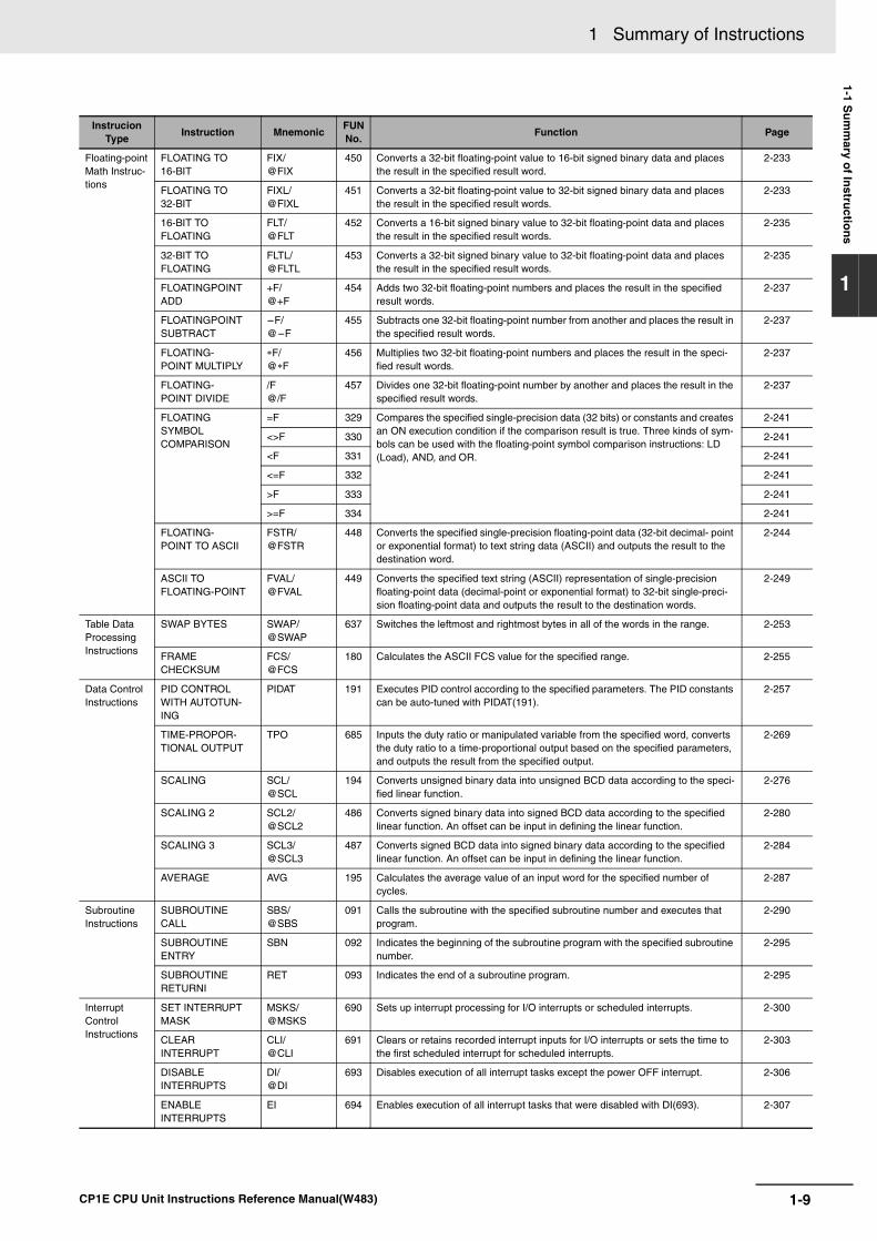
1 Summary of Instructions1-1 S
um
mary o
f Instru
ction
s
1
Floating-point Math Instruc-tions
FLOATING TO 16-BIT
FIX/@FIX
450 Converts a 32-bit floating-point value to 16-bit signed binary data and places the result in the specified result word.
2-233
FLOATING TO32-BIT
FIXL/@FIXL
451 Converts a 32-bit floating-point value to 32-bit signed binary data and places the result in the specified result words.
2-233
16-BIT TO FLOATING
FLT/@FLT
452 Converts a 16-bit signed binary value to 32-bit floating-point data and places the result in the specified result words.
2-235
32-BIT TOFLOATING
FLTL/@FLTL
453 Converts a 32-bit signed binary value to 32-bit floating-point data and places the result in the specified result words.
2-235
FLOATINGPOINTADD
+F/@+F
454 Adds two 32-bit floating-point numbers and places the result in the specified result words.
2-237
FLOATINGPOINTSUBTRACT
-F/@-F
455 Subtracts one 32-bit floating-point number from another and places the result in the specified result words.
2-237
FLOATING-POINT MULTIPLY
∗F/@∗F
456 Multiplies two 32-bit floating-point numbers and places the result in the speci-fied result words.
2-237
FLOATING-POINT DIVIDE
/F @/F
457 Divides one 32-bit floating-point number by another and places the result in the specified result words.
2-237
FLOATING SYMBOLCOMPARISON
=F 329 Compares the specified single-precision data (32 bits) or constants and creates an ON execution condition if the comparison result is true. Three kinds of sym-bols can be used with the floating-point symbol comparison instructions: LD (Load), AND, and OR.
2-241
<>F 330 2-241
<F 331 2-241
<=F 332 2-241
>F 333 2-241
>=F 334 2-241
FLOATING-POINT TO ASCII
FSTR/@FSTR
448 Converts the specified single-precision floating-point data (32-bit decimal- point or exponential format) to text string data (ASCII) and outputs the result to the destination word.
2-244
ASCII TO FLOATING-POINT
FVAL/@FVAL
449 Converts the specified text string (ASCII) representation of single-precision floating-point data (decimal-point or exponential format) to 32-bit single-preci-sion floating-point data and outputs the result to the destination words.
2-249
Table Data Processing Instructions
SWAP BYTES SWAP/@SWAP
637 Switches the leftmost and rightmost bytes in all of the words in the range. 2-253
FRAME CHECKSUM
FCS/@FCS
180 Calculates the ASCII FCS value for the specified range. 2-255
Data Control Instructions
PID CONTROLWITH AUTOTUN-ING
PIDAT 191 Executes PID control according to the specified parameters. The PID constants can be auto-tuned with PIDAT(191).
2-257
TIME-PROPOR-TIONAL OUTPUT
TPO 685 Inputs the duty ratio or manipulated variable from the specified word, converts the duty ratio to a time-proportional output based on the specified parameters, and outputs the result from the specified output.
2-269
SCALING SCL/@SCL
194 Converts unsigned binary data into unsigned BCD data according to the speci-fied linear function.
2-276
SCALING 2 SCL2/@SCL2
486 Converts signed binary data into signed BCD data according to the specified linear function. An offset can be input in defining the linear function.
2-280
SCALING 3 SCL3/@SCL3
487 Converts signed BCD data into signed binary data according to the specified linear function. An offset can be input in defining the linear function.
2-284
AVERAGE AVG 195 Calculates the average value of an input word for the specified number of cycles.
2-287
Subroutine Instructions
SUBROUTINECALL
SBS/@SBS
091 Calls the subroutine with the specified subroutine number and executes that program.
2-290
SUBROUTINEENTRY
SBN 092 Indicates the beginning of the subroutine program with the specified subroutine number.
2-295
SUBROUTINERETURNI
RET 093 Indicates the end of a subroutine program. 2-295
Interrupt Control Instructions
SET INTERRUPTMASK
MSKS/@MSKS
690 Sets up interrupt processing for I/O interrupts or scheduled interrupts. 2-300
CLEARINTERRUPT
CLI/@CLI
691 Clears or retains recorded interrupt inputs for I/O interrupts or sets the time to the first scheduled interrupt for scheduled interrupts.
2-303
DISABLE INTERRUPTS
DI/@DI
693 Disables execution of all interrupt tasks except the power OFF interrupt. 2-306
ENABLE INTERRUPTS
EI 694 Enables execution of all interrupt tasks that were disabled with DI(693). 2-307
Instrucion Type
Instruction MnemonicFUNNo.
Function Page
1-9CP1E CPU Unit Instructions Reference Manual(W483)
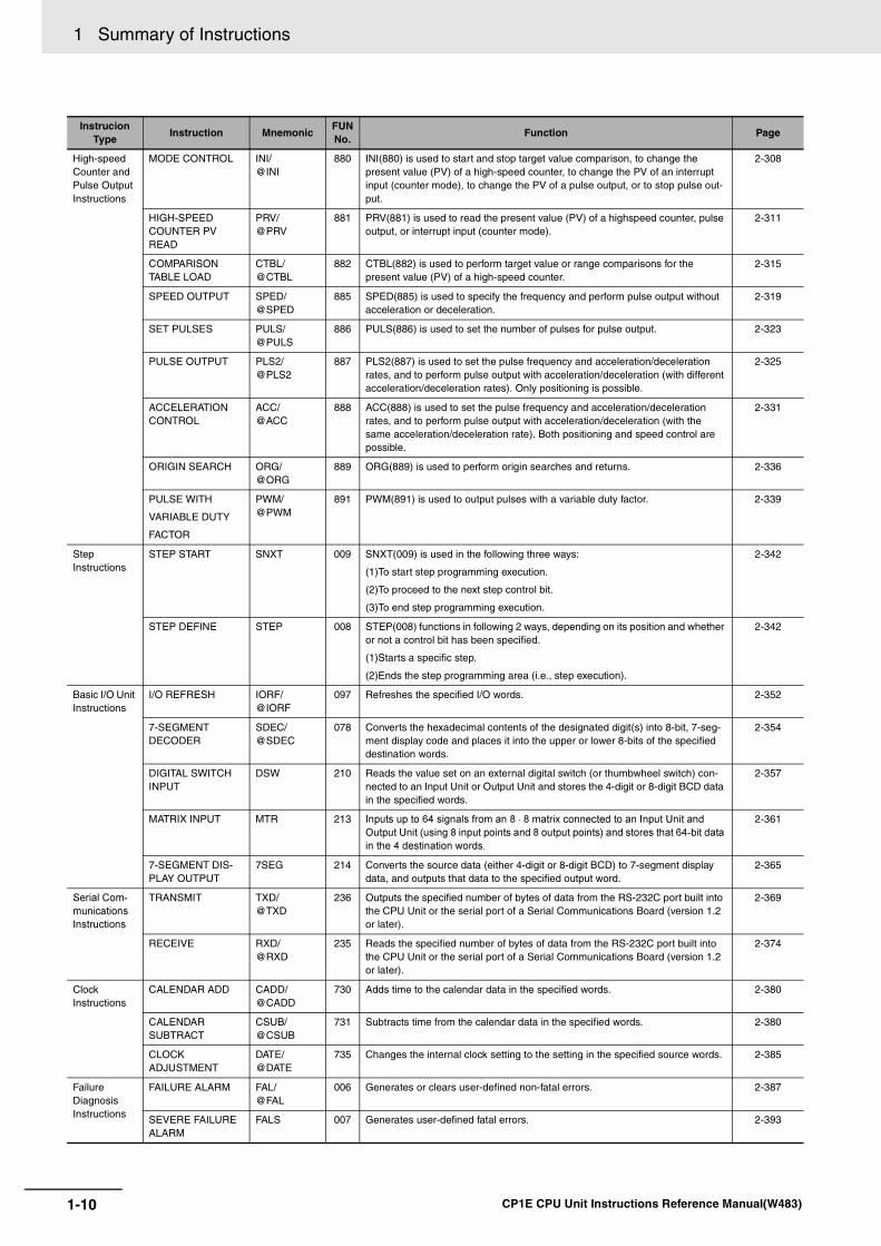
1 Summary of Instructions
High-speed Counter and Pulse Output Instructions
MODE CONTROL INI/@INI
880 INI(880) is used to start and stop target value comparison, to change the present value (PV) of a high-speed counter, to change the PV of an interrupt input (counter mode), to change the PV of a pulse output, or to stop pulse out-put.
2-308
HIGH-SPEEDCOUNTER PVREAD
PRV/@PRV
881 PRV(881) is used to read the present value (PV) of a highspeed counter, pulse output, or interrupt input (counter mode).
2-311
COMPARISONTABLE LOAD
CTBL/@CTBL
882 CTBL(882) is used to perform target value or range comparisons for the present value (PV) of a high-speed counter.
2-315
SPEED OUTPUT SPED/@SPED
885 SPED(885) is used to specify the frequency and perform pulse output without acceleration or deceleration.
2-319
SET PULSES PULS/@PULS
886 PULS(886) is used to set the number of pulses for pulse output. 2-323
PULSE OUTPUT PLS2/@PLS2
887 PLS2(887) is used to set the pulse frequency and acceleration/deceleration rates, and to perform pulse output with acceleration/deceleration (with different acceleration/deceleration rates). Only positioning is possible.
2-325
ACCELERATIONCONTROL
ACC/@ACC
888 ACC(888) is used to set the pulse frequency and acceleration/deceleration rates, and to perform pulse output with acceleration/deceleration (with the same acceleration/deceleration rate). Both positioning and speed control are possible.
2-331
ORIGIN SEARCH ORG/@ORG
889 ORG(889) is used to perform origin searches and returns. 2-336
PULSE WITH
VARIABLE DUTY
FACTOR
PWM/@PWM
891 PWM(891) is used to output pulses with a variable duty factor. 2-339
Step Instructions
STEP START SNXT 009 SNXT(009) is used in the following three ways:
(1)To start step programming execution.
(2)To proceed to the next step control bit.
(3)To end step programming execution.
2-342
STEP DEFINE STEP 008 STEP(008) functions in following 2 ways, depending on its position and whether or not a control bit has been specified.
(1)Starts a specific step.
(2)Ends the step programming area (i.e., step execution).
2-342
Basic I/O Unit Instructions
I/O REFRESH IORF/@IORF
097 Refreshes the specified I/O words. 2-352
7-SEGMENTDECODER
SDEC/@SDEC
078 Converts the hexadecimal contents of the designated digit(s) into 8-bit, 7-seg-ment display code and places it into the upper or lower 8-bits of the specified destination words.
2-354
DIGITAL SWITCHINPUT
DSW 210 Reads the value set on an external digital switch (or thumbwheel switch) con-nected to an Input Unit or Output Unit and stores the 4-digit or 8-digit BCD data in the specified words.
2-357
MATRIX INPUT MTR 213 Inputs up to 64 signals from an 8 ⋅ 8 matrix connected to an Input Unit and
Output Unit (using 8 input points and 8 output points) and stores that 64-bit data
in the 4 destination words.
2-361
7-SEGMENT DIS-PLAY OUTPUT
7SEG 214 Converts the source data (either 4-digit or 8-digit BCD) to 7-segment display data, and outputs that data to the specified output word.
2-365
Serial Com-
munications
Instructions
TRANSMIT TXD/@TXD
236 Outputs the specified number of bytes of data from the RS-232C port built into the CPU Unit or the serial port of a Serial Communications Board (version 1.2 or later).
2-369
RECEIVE RXD/@RXD
235 Reads the specified number of bytes of data from the RS-232C port built into the CPU Unit or the serial port of a Serial Communications Board (version 1.2 or later).
2-374
Clock Instructions
CALENDAR ADD CADD/@CADD
730 Adds time to the calendar data in the specified words. 2-380
CALENDARSUBTRACT
CSUB/@CSUB
731 Subtracts time from the calendar data in the specified words. 2-380
CLOCKADJUSTMENT
DATE/@DATE
735 Changes the internal clock setting to the setting in the specified source words. 2-385
Failure Diagnosis Instructions
FAILURE ALARM FAL/@FAL
006 Generates or clears user-defined non-fatal errors. 2-387
SEVERE FAILURE ALARM
FALS 007 Generates user-defined fatal errors. 2-393
Instrucion Type
Instruction MnemonicFUNNo.
Function Page
1-10 CP1E CPU Unit Instructions Reference Manual(W483)

1 Summary of Instructions1-1 S
um
mary o
f Instru
ction
s
1
Other Instructions
SET CARRY STC/@STC
040 Sets the Carry Flag (CY). 2-398
CLEAR CARRY CLC/@CLC
041 Turns OFF the Carry Flag (CY). 2-398
EXTEND MAXIMUMCYCLE TIME
WDT/@WDT
094 Extends the maximum cycle time, but only for the cycle in which this instruction is executed.
2-399
Instrucion Type
Instruction MnemonicFUNNo.
Function Page
1-11CP1E CPU Unit Instructions Reference Manual(W483)

1 Summary of Instructions
1-12 CP1E CPU Unit Instructions Reference Manual(W483)
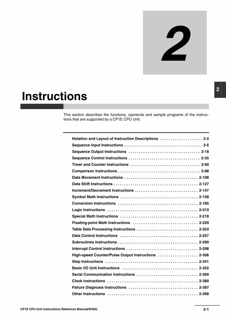
22
This section describes the functions, operands and sample programs of the instruc-tions that are supported by a CP1E CPU Unit.
Notation and Layout of Instruction Descriptions . . . . . . . . . . . . . . . . . . . . 2-2
Sequence Input Instructions . . . . . . . . . . . . . . . . . . . . . . . . . . . . . . . . . . . . . 2-5
Sequence Output Instructions . . . . . . . . . . . . . . . . . . . . . . . . . . . . . . . . . . 2-18
Sequence Control Instructions . . . . . . . . . . . . . . . . . . . . . . . . . . . . . . . . . . 2-35
Timer and Counter Instructions . . . . . . . . . . . . . . . . . . . . . . . . . . . . . . . . . 2-60
Comparison Instructions . . . . . . . . . . . . . . . . . . . . . . . . . . . . . . . . . . . . . . . 2-88
Data Movement Instructions . . . . . . . . . . . . . . . . . . . . . . . . . . . . . . . . . . . 2-108
Data Shift Instructions . . . . . . . . . . . . . . . . . . . . . . . . . . . . . . . . . . . . . . . . 2-127
Increment/Decrement Instructions . . . . . . . . . . . . . . . . . . . . . . . . . . . . . . 2-147
Symbol Math Instructions . . . . . . . . . . . . . . . . . . . . . . . . . . . . . . . . . . . . . 2-158
Conversion Instructions . . . . . . . . . . . . . . . . . . . . . . . . . . . . . . . . . . . . . . 2-185
Logic Instructions . . . . . . . . . . . . . . . . . . . . . . . . . . . . . . . . . . . . . . . . . . . 2-210
Special Math Instructions . . . . . . . . . . . . . . . . . . . . . . . . . . . . . . . . . . . . . 2-218
Floating-point Math Instructions . . . . . . . . . . . . . . . . . . . . . . . . . . . . . . . 2-229
Table Data Processing Instructions . . . . . . . . . . . . . . . . . . . . . . . . . . . . . 2-253
Data Control Instructions . . . . . . . . . . . . . . . . . . . . . . . . . . . . . . . . . . . . . 2-257
Subroutines Instructions . . . . . . . . . . . . . . . . . . . . . . . . . . . . . . . . . . . . . . 2-290
Interrupt Control Instructions . . . . . . . . . . . . . . . . . . . . . . . . . . . . . . . . . . 2-298
High-speed Counter/Pulse Output Instructions . . . . . . . . . . . . . . . . . . . 2-308
Step Instructions . . . . . . . . . . . . . . . . . . . . . . . . . . . . . . . . . . . . . . . . . . . . 2-341
Basic I/O Unit Instructions . . . . . . . . . . . . . . . . . . . . . . . . . . . . . . . . . . . . 2-352
Serial Communication Instructions . . . . . . . . . . . . . . . . . . . . . . . . . . . . . 2-369
Clock Instructions . . . . . . . . . . . . . . . . . . . . . . . . . . . . . . . . . . . . . . . . . . . 2-380
Failure Diagnosis Instructions . . . . . . . . . . . . . . . . . . . . . . . . . . . . . . . . . 2-387
Other Instructions . . . . . . . . . . . . . . . . . . . . . . . . . . . . . . . . . . . . . . . . . . . 2-398
Instructions
2-1CP1E CPU Unit Instructions Reference Manual(W483)

2 Instructions
Notation and Layout of Instruction Descriptions
Instructions are described in groups by function. Refer to Appendix A List of Instructions by FunctionCode for a list of instructions by mnemonic that lists the page number in this section for each instruc-tion.
The description of each instruction is organized as described in the following table.
Item Contents
Instruction Indicates the name of the instruction. Example: MOVE BIT
Mnemonic Indicates the mnemonic.
Example: MOVB(082)
Variations Differentiation
@ Instruction that differentiates when the execution condition turns ON.
% Instruction that differentiates when the execution condition turns OFF.
Immediate refreshing
! Refreshes data in the I/O area specified by the operands or the Special I/O Unit words when the instruction is executed.
Function code Indicates the function code.
Function The basic purpose of the instruction is described after the section heading.
Symbol The ladder symbol used to represent the instruction on the CX-Programmer is shown, as in the exam-ple for the MOVE BIT instruction given below. The name of each operand is also provided with the lad-der symbol.
Applicable Program Areas The program areas in which the instruction can be used are specified. “OK” indicates the areas in which the instruction can be used.
Operands Indicates a description of the operand, the data type, and the size.
Where necessary, the meaning of words and bits used in specific operands, such as control words, is given.
Operand Specifications The memory areas addresses that can be used each operand are listed in a table like the following one. The letters used in the column headings on the above are the same as those used in the ladder symbol. “---” is used to indicate when an area cannot be specific for an operand.
repeatedly as long aexecution condition
a
A
JMP
N
MOVB
S
C
D
S: Source word or data
C: Control word
D: Destination word
Area Step program areas Subroutines Interrupt tasks
Usage OK OK OK
15 8 07C m n
Source bit: 00 to 0F(0 to 15 decimal)
Destination bit: 00 to 0F (0 to 15 decimal)
Word addresses Indirect DMaddresses
CIO WR HR AR T C DM @DM *DMS
OK OK OK OK OK OK OK OK OKOK
--- ---CD ---
---
Area Con-stants CF TR
bitsPulsebits
2-2 CP1E CPU Unit Instructions Reference Manual(W483)

2 Instructions N
otatio
n an
d L
ayou
t of
Instru
ction
Descrip
tion
s
2
ConstantsConstants input for operands are given as listed below.
Operand Descriptions and Operand Specifications
• Operands Specifying Bit Strings (Normally Input as Hexadecimal):Only the hexadecimal form is given for operands specifying bit strings, e.g., only “#0000 to #FFFF” isspecified as the S operand for the MOV(021) instruction. On the CX-Programmer, however, bit stringscan be input in decimal form by using the & prefix.
• Operands Specifying Numeric Values (Normally Input as Decimal, Including Jump Numbers):Both the decimal and hexadecimal forms are given for operands specifying numeric values, e.g.,“#0000 to #FFFF” and “&0 to &65535” are given for the N operand for the XFER(070) instruction.
• Operands Indicating Control Numbers (Except for Jump Numbers):The decimal form is given for control numbers, e.g., “0 to 1023” is given for the N operand for theSBS(091) instruction.
ExamplesIn the examples, constants are given using the CX-Programmer notation, e.g., operands specifyingnumeric values are given in decimal for with an & prefix, as shown in the following example.
The input methods for constants for the Programming Devices are given in the following table.
Note When operands are input on the CX-Programmer, the input ranges will be displayed along with the appropri-ate prefixes.
Flags The flags table indicates the status of the condition flags immediately after execution of the instruction. Any flags that are not listed are not affected by the instruction. “OFF” indicates that a flag is turned OFF immediately after execution of the instruction regardless of the results of executing the instruc-tion.
Function Indicates the function of the instruction.
Hint Indicates a supplemental explanation of other than the main function.
Precautions Indicates important points when using an instruction.
Sample program An example of using the instruction with specific operands is provided to further explain the function of the instruction.
Operand CX-Programmer
Operands specifying bit strings (normally input as hexadeci-mal)
Input as decimal with an & prefix or input as hexadecimal with an # prefix. (See note.)
Operands specifying numeric values (normally input as deci-mal)
Operands specifying control numbers (except for jump num-bers)
Input as decimal with an # prefix. (See note.)
Item Contents
Name Label Operation
Error Flag ER OFF
Equal Flag = • ON if the data being transferred (D) is 0. • OFF in all other cases.
Negative Flag N • ON if the leftmost bit of the data being transferred (D) is 1.• OFF in all other cases.
XFER
&10
D100
D200
2-3CP1E CPU Unit Instructions Reference Manual(W483)

2 Instructions
Condition FlagsWith the CX-Programmer, the condition flags are registered in advance as global symbols with “P_” infront of the symbol name.
Symbol InstructionsSome of the C/CV-series PLC instructions have been changed to different instructions with the samefunctionality for the CP1E-series PLCs.
Flag CX-Programmer label
Error Flag P_ER
Access Error Flag P_AER
Carry Flag P_CY
Greater Than Flag P_GT
Equals Flag P_EQ
Less Than Flag P_LT
Negative Flag P_N
Overflow Flag P_OF
Underflow Flag P_UF
Greater Than or Equals Flag P_GE
Not Equal Flag P_NE
Less Than or Equals Flag P_LE
Always ON Flag P_On
Always OFF Flag P_Off
Instruction group C/CV Series CP1E Series
Comparison EQU AND=
Data Movement MOVQ MOV
Increment/Decrement INC ++B
INCL ++BL
INCB ++
INBL ++L
DEC --B
DECL --BL
DECB --
DCBL --L
Symbol Math ADB +C
ADBL +CL
ADD +BC
ADDL +BCL
SBB -C
SBBL -CL
SUB -BC
SUBL -BCL
MBS *
MBSL *L
MUL *B
MULL *BL
DBS /
DBSL /L
DIV /B
DIVL /BL
Interrupt Control INT MSKS / CLIDI / EI
2-4 CP1E CPU Unit Instructions Reference Manual(W483)
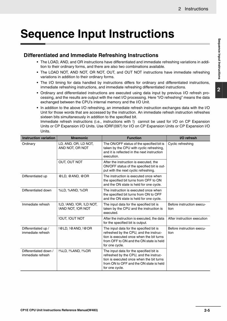
2 Instructions S
equ
ence In
pu
t Instru
ction
s
2
Sequence Input Instructions
Differentiated and Immediate Refreshing Instructions• The LOAD, AND, and OR instructions have differentiated and immediate refreshing variations in addi-
tion to their ordinary forms, and there are also two combinations available.
• The LOAD NOT, AND NOT, OR NOT, OUT, and OUT NOT instructions have immediate refreshingvariations in addition to their ordinary forms.
• The I/O timing for data handled by instructions differs for ordinary and differentiated instructions,immediate refreshing instructions, and immediate refreshing differentiated instructions.
• Ordinary and differentiated instructions are executed using data input by previous I/O refresh pro-cessing, and the results are output with the next I/O processing. Here “I/O refreshing” means the dataexchanged between the CPU’s internal memory and the I/O Unit.
• In addition to the above I/O refreshing, an immediate refresh instruction exchanges data with the I/OUnit for those words that are accessed by the instruction. An immediate refresh instruction refreshessixteen bits simultaneously in addition to the specified bit.Immediate refresh instructions (i.e., instructions with !) cannot be used for I/O on CP ExpansionUnits or CP Expansion I/O Units. Use IORF(097) for I/O on CP Expansion Units or CP Expansion I/OUnits.
Instruction variation Mnemonic Function I/O refresh
Ordinary LD, AND, OR, LD NOT, AND NOT, OR NOT
The ON/OFF status of the specified bit is taken by the CPU with cyclic refreshing, and it is reflected in the next instruction execution.
Cyclic refreshing
OUT, OUT NOT After the instruction is executed, the ON/OFF status of the specified bit is out-put with the next cyclic refreshing.
Differentiated up @LD, @AND, @OR The instruction is executed once when the specified bit turns from OFF to ON and the ON state is held for one cycle.
Differentiated down %LD, %AND, %OR The instruction is executed once when the specified bit turns from ON to OFF and the ON state is held for one cycle.
Immediate refresh !LD, !AND, !OR, !LD NOT, !AND NOT, !OR NOT
The input data for the specified bit is taken by the CPU and the instruction is executed.
Before instruction execu-tion
!OUT, !OUT NOT After the instruction is executed, the data for the specified bit is output.
After instruction execution
Differentiated up / immediate refresh
!@LD, !@AND, !@OR The input data for the specified bit is refreshed by the CPU, and the instruc-tion is executed once when the bit turns from OFF to ON and the ON state is held for one cycle.
Before instruction execu-tion
Differentiated down / immediate refresh
!%LD, !%AND, !%OR The input data for the specified bit is refreshed by the CPU, and the instruc-tion is executed once when the bit turns from ON to OFF and the ON state is held for one cycle.
2-5CP1E CPU Unit Instructions Reference Manual(W483)

2 Instructions
Operation Timing for I/O InstructionsThe following chart shows the differences in the timing of instruction operations for a program config-ured from LD and OUT.
A
A
A
A
A
A
A
A
A
A
A
A
B1
B2
B3
B4
B5
B6
B7
B8
B9
B10
B11
B12
!
!
!
!
!
A
B1
B2
B3
B4
B5
B6
B7
B8
B9
B10
B11
B12!
↓
↑
!
!
!↓
!↑
!
↓
↑
!↓
!↑
I/O refreshingInstruction execution
CPU processing
Input received
Input received
Input received
Input received
Input received
Input received
Input received
Input received
Input received
Input received
Input receivedInput received
2-6 CP1E CPU Unit Instructions Reference Manual(W483)

2 Instructions S
equ
ence In
pu
t Instru
ction
s
2
LD/LD
NO
T
LD/LD NOT
Applicable Program Areas
Operands
Operand Specifications
FlagsThere are no flags affected by this instruction.
Function
LDLD is used for the first normally open bit from the bus bar or for the first normally open bit of a logicblock. If there is no immediate refreshing specification, the specified bit in I/O memory is read. If there isan immediate refreshing specification, the status of the CPU Unit’s built-in input terminal is read andused.
LD NOTLD NOT is used for the first normally closed bit from the bus bar, or for the first normally closed bit of alogic block. If there is no immediate refreshing specification, the specified bit in I/O memory is read andreversed. If there is an immediate refreshing specification, the status of the CPU Unit’s built-in input ter-minal is read, reversed, and used.
Instruction Mnemonic VariationsFunction
codeFunction
LOAD LD@LD, %LD, !LD, !@LD, !%LD
---Indicates a logical start and creates an ON/OFF execution condition based on the ON/OFF status of the specified operand bit.
LOAD NOT LD NOT
@LD NOT, %LD NOT, ! LD NOT, !@LD NOT, !%LD NOT
---Indicates a logical start and creates an ON/OFF execution condition based on the reverse of the ON/OFF status of the specified operand bit.
Symbol
LD LD NOT
Area Step program areas Subroutines Interrupt tasks
Usage OK OK OK
Operand Description Data type Size
--- --- BOOL ---
Area Word addresses Indirect DM addresses
Constants CF Pulse bits TR bitsCIO WR HR AR T C DM @DM *DM
LDOK OK OK OK OK OK --- --- --- --- OK OK
OK
LD NOT ---
Bus bar Starting point of block Bus bar Starting point of block
2-7CP1E CPU Unit Instructions Reference Manual(W483)

2 Instructions
Hint• LD/LD NOT is used in the following circumstances as an instruction for indicating a logical start.
1. When directly connecting to the bus bar.
2. When logic blocks are connected by AND LD or OR LD, i.e., at the beginning of a logic block.The AND LOAD and OR LOAD instructions are used to connect in series or in parallel logic blocksbeginning with LD or LD NOT.
• At least one LOAD or LOAD NOT instruction is required for the execution condition when output-related instructions cannot be connected directly to the bus bar. If there is no LOAD or LOAD NOTinstruction, a programming error will occur with the program check by the Peripheral Device.
• When logic blocks are connected by AND LOAD or OR LOAD instructions, the total number of ANDLOAD/OR LOAD instructions must match the total number of LOAD/LOAD NOT instructions minus1.If they do not match, a programming error will occur. For details, refer to AND LOAD: AND LD andOR LOAD: OR LD.
Precautions• Differentiate up (@) or differentiate down (%) can be specified for LD. If differentiate up (@) is speci-
fied, the execution condition is turned ON for one cycle only after the status of the operand bit goesfrom OFF to ON. If differentiate down (%) is specified, the execution condition is turned ON for onecycle only after the status of the operand bit goes from ON to OFF.
• Immediate refreshing (!) can be specified for LD/LD NOT. An immediate refresh instruction updatesthe status of the built-in input bit just before the instruction is executed from the CPU Unit.
• For LD, it is possible to combine immediate refreshing and up or down differentiation (!@ or !%). Ifeither of these is specified, the input is refreshed from the Basic Input Unit just before the instructionis executed and the execution condition is turned ON for one cycle only after the status goes fromOFF to ON, or from ON to OFF.
Sample programi
100.00
0.05LD NOT
LD LD
LD
Instruction Operand
LD 0.00
LD 0.01
LD 0.02
AND 0.03
OR LD --
AND LD --
LD NOT 0.04
AND 0.05
OR LD --
OUT 100.00
OR LDAND LD
OR LD
0.02
0.010.00
0.04
0.03
2-8 CP1E CPU Unit Instructions Reference Manual(W483)

2 Instructions S
equ
ence In
pu
t Instru
ction
s
2
AN
D/A
ND
NO
T
AND/AND NOT
Applicable Program Areas
Operands
Operand Specifications
FlagsThere are no flags affected by this instruction.
Function
ANDAND is used for a normally open bit connected in series. AND cannot be directly connected to the busbar, and cannot be used at the beginning of a logic block. If there is no immediate refreshing specifica-tion, the specified bit in I/O memory is read. If there is an immediate refreshing specification, the statusof the CPU Unit’s built-in input terminal is read.
AND NOTAND NOT is used for a normally closed bit connected in series. AND NOT cannot be directly connectedto the bus bar, and cannot be used at the beginning of a logic block. If there is no immediate refreshingspecification, the specified bit in I/O memory is read. If there is an immediate refreshing specification,the status the CPU Unit’s built-in input terminals is read.
Instruction Mnemonic VariationsFunction
codeFunction
AND AND@AND, %AND, !AND, !@AND, !%AND
---Takes a logical AND of the status of the specified operand bit and the current execution condition.
AND NOT AND NOT
@AND NOT, %AND NOT, !AND NOT, !@AND NOT, !%AND NOT
---Reverses the status of the specified operand bit and takes a logical AND with the current execution condition.
Symbol
AND AND NOT
Area Step program areas Subroutines Interrupt tasks
Usage OK OK OK
Operand Description Data type Size
--- --- BOOL ---
Area Word addresses Indirect DM addresses
Constants CF Pulse bits TR bitsCIO WR HR AR T C DM @DM *DM
ANDOK OK OK OK OK OK --- --- --- --- OK OK ---
AND NOT
2-9CP1E CPU Unit Instructions Reference Manual(W483)

2 Instructions
Precautions• Differentiate up (@) or differentiate down (%) can be specified for AND. If differentiate up (@) is spec-
ified, the execution condition is turned ON for one cycle only after the status of the operand bit goesfrom OFF to ON. If differentiate down (%) is specified, the execution condition is turned ON for onecycle only after the status of the operand bit goes from ON to OFF.
• Immediate refreshing (!) can be specified for AND/AND NOT. An immediate refresh instructionupdates the status of the built-in input bit just before the instruction is executed from the CPU Unit.
• For AND, it is possible to combine immediate refreshing and up or down differentiation (!@ or !%). Ifeither of these is specified, the input is refreshed from the Basic Input Unit just before the instructionis executed and the execution condition is turned ON for one cycle only after the status goes fromOFF to ON, or from ON to OFF.
Sample programi
0.04
0.010.00 100.00
0.05
AND
AND NOT
Instruction Operand
LD 0.00
AND 0.01
LD 0.02
AND 0.03
LD 0.04
AND NOT 0.05
OR LD --
AND LD --
OUT 100.00
0.030.02
AND
2-10 CP1E CPU Unit Instructions Reference Manual(W483)

2 Instructions S
equ
ence In
pu
t Instru
ction
s
2
OR
/OR
NO
T
OR/OR NOT
Applicable Program Areas
Operands
Operand Specifications
FlagsThere are no flags affected by this instruction.
Function
Instruction Mnemonic VariationsFunction
codeFunction
OR OR@OR, %OR, !OR, !@OR, !%OR
---Takes a logical OR of the ON/OFF status of the specified operand bit and the current execution condition.
OR NOT OR NOT
@OR NOT, %OR NOT, !OR NOT, !@OR NOT, !%OR NOT
---Reverses the status of the specified bit and takes a logical OR with the current execution condition.
Symbol
OR OR NOT
Area Step program areas Subroutines Interrupt tasks
Usage OK OK OK
Operand Description Data type Size
--- --- BOOL ---
Area Word addresses Indirect DM addresses
Constants CF Pulse bits TR bitsCIO WR HR AR T C DM @DM *DM
OROK OK OK OK OK OK --- --- --- --- OK OK ---
OR NOT
OROR is used for a normally open bit connected in parallel. A normally open bit is configured to form a log-ical OR with a logic block beginning with a LOAD or LOAD NOT instruction (connected to the bus bar orat the beginning of the logic block). If there is no immediate refreshing specification, the specified bit inI/O memory is read. If there is an immediate refreshing specification, the status of the CPU Unit’s built-in input terminal is read.
OR NOTOR NOT is used for a normally closed bit connected in parallel. A normally closed bit is configured toform a logical OR with a logic block beginning with a LOAD or LOAD NOT instruction (connected to thebus bar or at the beginning of the logic block). If there is no immediate refreshing specification, thespecified bit in I/O memory is read. If there is an immediate refreshing specification, the status of theCPU Unit’s built-in input terminal is read.
Bus bar Bus bar
2-11CP1E CPU Unit Instructions Reference Manual(W483)

2 Instructions
Precautions• Differentiate up (@) or differentiate down (%) can be specified for OR. If differentiate up (@) is speci-
fied, the execution condition is turned ON for one cycle only after the status of the operand bit goesfrom OFF to ON. If differentiate down (%) is specified, the execution condition is turned ON for onecycle only after the status of the operand bit goes from ON to OFF.
• Immediate refreshing (!) can be specified for OR/OR NOT. An immediate refresh instruction updatesthe status of the built-in input bit just before the instruction is executed from the CPU Unit.
• For OR, it is possible to combine immediate refreshing and up or down differentiation (!@ or !%). Ifeither of these is specified, the input is refreshed from the Basic Input Unit just before the instructionis executed and the execution condition is turned ON for one cycle only after the status of the oper-and bit goes from OFF to ON, or from ON to OFF.
Sample programi
0.00 100.00
OR OR NOT
Instruction Operand
LD 0.00
AND 0.01
AND 0.02
OR 0.03
AND 0.04
LD 0.05
AND 0.06
OR NOT 0.07
AND LD --
OUT 100.00
0.01 0.02 0.04 0.05
0.03 0.07
0.06
2-12 CP1E CPU Unit Instructions Reference Manual(W483)

2 Instructions S
equ
ence In
pu
t Instru
ction
s
2
AN
D LD
/OR
LD
AND LD/OR LD
Applicable Program Areas
FlagsThere are no flags affected by this instruction.
Function
Hint
Instruction Mnemonic VariationsFunction
codeFunction
AND LOAD AND LD --- --- Takes a logical AND between logic blocks.
OR LOAD OR LD --- --- Takes a logical OR between logic blocks.
Symbol
AND LD OR LD
Area Step program areas Subroutines Interrupt tasks
Usage OK OK OK
AND LDAND LD connects in series the logic block justbefore this instruction with another logic block.
The logic block consists of all the instructionsfrom a LOAD or LOAD NOT instruction untiljust before the next LOAD or LOAD NOTinstruction on the same rungs.
OR LDOR LD connects in parallel the logic block justbefore this instruction with another logic block.
The logic block consists of all the instructionsfrom a LOAD or LOAD NOT instruction untiljust before the next LOAD or LOAD NOTinstruction on the same rungs.
AND LD• Three or more logic blocks can be connected in series using this instruction to first connect two of the
logic blocks and then to connect the next and subsequent ones in order. It is also possible to continueplacing this instruction after three or more logic blocks and connect them together in series.
OR LD• Three or more logic blocks can be connected in parallel using this instruction to first connect two of
the logic blocks and then to connect the next and subsequent ones in order. It is also possible to con-tinue placing this instruction after three or more logic blocks and connect them together in parallel.
Logic block Logic block
Logic block
Logic block
LD
LD
AND LD
Logic block A
Logic block B
Serial connection between logic block A and logic block B.
to
to
LD
LD
OR LD
to
to
Logic block A
Logic block B
Parallel connection between logic block A and logic block B.
2-13CP1E CPU Unit Instructions Reference Manual(W483)

2 Instructions
PrecautionsWhen a logic block is connected by AND LOAD or OR LOAD instructions, the total number of ANDLOAD/OR LOAD instructions must match the total number of LOAD/LOAD NOT instructions minus 1. Ifthey do not match, a programming error will occur.
AND LDIn the following diagram, the two logic blocks are indicated by dotted lines. Studying this example showsthat an ON execution condition will be produced when either of the execution conditions in the left logicblock is ON (i.e., when either CIO 0.00 or CIO 0.01 is ON) and either of the execution conditions in theright logic block is ON (i.e., when either CIO 0.02 is ON or CIO 0.03 is OFF).
i
OR LDThe following diagram requires an OR LOAD instruction between the top logic block and the bottomlogic block. An ON execution condition would be produced either when CIO 0.00 is ON and CIO 0.01 isOFF or when CIO 0.02 and CIO 0.03 are both ON. The operation of and mnemonic code for the ORLOAD instruction is exactly the same as those for a AND LOAD instruction except that the current exe-cution condition is ORed with the last unused execution condition.
i
0.00 0.02
0.030.01
100.00 Coding
Second LD: Used for first bit of next block connected in series to previous block.
Instruction Operand
LD 0.00
OR 0.01
LD 0.02
OR NOT 0.03
AND LD ---
OUT 100.00
0.00 0.01
0.030.02
100.01 Coding
Second LD: Used for first bit of next block connected in series to previous block.
Instruction Operand
LD 0.00
AND NOT 0.01
LD 0.02
AND 0.03
OR LD ---
OUT 100.01
2-14 CP1E CPU Unit Instructions Reference Manual(W483)

2 Instructions S
equ
ence In
pu
t Instru
ction
s
2
AN
D LD
/OR
LD
Sample program AND LD
i
• The AND LOAD instruction can be used repeatedly. In programming method (2) above, however, thenumber of AND LOAD instructions becomes one less than the number of LOAD and LOAD NOTinstructions before that.
• In method (2), make sure that the total number of LOAD and LOAD NOT instructions before ANDLOAD is not more than eight.
• To use nine or more, program using method (1).
• If there are nine or more with method (2), then a program error will occur during the program check bythe Peripheral Device.
OR LDi
• The OR LOAD instruction can be used repeatedly. In programming method (2) above, however, thenumber of OR LOAD instructions becomes one less than the number of LOAD and LOAD NOTinstructions before that.
• In method (2), make sure that the total number of LOAD and LOAD NOT instructions before ORLOAD is not more than eight.
• To use nine or more, program using method (1).
• If there are nine or more with method (2), then a program error will occur during the program check bythe Peripheral Device.
0.00 0.02
0.03
0.04
0.050.01
100.00 Coding Example (1) Coding Example (2)
Instruction Operand
LD 0.00
OR NOT 0.01
LD NOT 0.02
OR 0.03
AND LD ---
LD 0.04
OR 0.05
AND LD ---
.
...
OUT 100.00
Instruction Operand
LD 0.00
OR NOT 0.01
LD NOT 0.02
OR 0.03
LD 0.04
OR 0.05
.
...
AND LD ---
AND LD ---
.
...
OUT 100.00
0.00 0.01
0.030.02
0.050.04
100.01 Coding Example (1) Coding Example (2)
Instruction Operand
LD 0.00
AND NOT 0.01
LD NOT 0.02
AND NOT 0.03
OR LD ---
LD 0.04
AND 0.05
OR LD ---
.
...
OUT 100.01
Instruction Operand
LD 0.00
AND NOT 0.01
LD NOT 0.02
AND NOT 0.03
LD 0.04
AND 0.05
.
...
OR LD ---
OR LD ---
.
...
OUT 100.01
2-15CP1E CPU Unit Instructions Reference Manual(W483)

2 Instructions
NOT
Applicable Program Areas
FlagsThere are no flags affected by NOT(520).
FunctionNOT(520) is placed between an execution condition and another instruction to invert the execution con-dition.
PrecautionsNOT(520) is an intermediate instruction, i.e., it cannot be used as a right-hand instruction. Be sure toprogram a right-hand instruction after NOT(520).
Sample programi
Instruction Mnemonic VariationsFunction
codeFunction
NOT NOT --- 520 Reverses the execution condition.
Symbol
NOT
Area Step program areas Subroutines Interrupt tasks
Usage OK OK OK
NOT(520)
100.00NOT(520) reverses the execution condition in the following example.
0.00 0.01
0.02
NOT(520)
0.00
1
1
1
0
1
0
0
0
0.01
1
1
0
1
0
1
0
0
0.02
1
0
1
1
0
0
1
0
100.00
0
0
1
0
1
1
1
1
2-16 CP1E CPU Unit Instructions Reference Manual(W483)
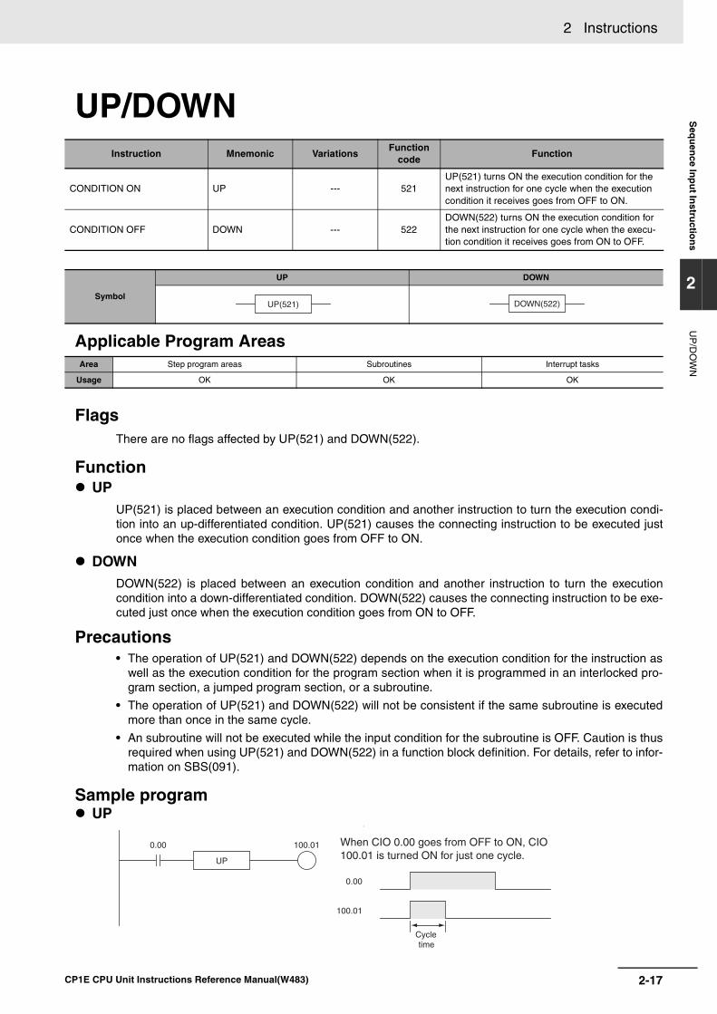
2 Instructions S
equ
ence In
pu
t Instru
ction
s
2
UP
/DO
WN
UP/DOWN
Applicable Program Areas
FlagsThere are no flags affected by UP(521) and DOWN(522).
Function
Precautions• The operation of UP(521) and DOWN(522) depends on the execution condition for the instruction as
well as the execution condition for the program section when it is programmed in an interlocked pro-gram section, a jumped program section, or a subroutine.
• The operation of UP(521) and DOWN(522) will not be consistent if the same subroutine is executedmore than once in the same cycle.
• An subroutine will not be executed while the input condition for the subroutine is OFF. Caution is thusrequired when using UP(521) and DOWN(522) in a function block definition. For details, refer to infor-mation on SBS(091).
Sample program UP
i
Instruction Mnemonic VariationsFunction
codeFunction
CONDITION ON UP --- 521UP(521) turns ON the execution condition for the next instruction for one cycle when the execution condition it receives goes from OFF to ON.
CONDITION OFF DOWN --- 522DOWN(522) turns ON the execution condition for the next instruction for one cycle when the execu-tion condition it receives goes from ON to OFF.
Symbol
UP DOWN
Area Step program areas Subroutines Interrupt tasks
Usage OK OK OK
UPUP(521) is placed between an execution condition and another instruction to turn the execution condi-tion into an up-differentiated condition. UP(521) causes the connecting instruction to be executed justonce when the execution condition goes from OFF to ON.
DOWNDOWN(522) is placed between an execution condition and another instruction to turn the executioncondition into a down-differentiated condition. DOWN(522) causes the connecting instruction to be exe-cuted just once when the execution condition goes from ON to OFF.
UP(521) DOWN(522)
UP
0.00 100.01
0.00
100.01
Cycle time
When CIO 0.00 goes from OFF to ON, CIO 100.01 is turned ON for just one cycle.
2-17CP1E CPU Unit Instructions Reference Manual(W483)
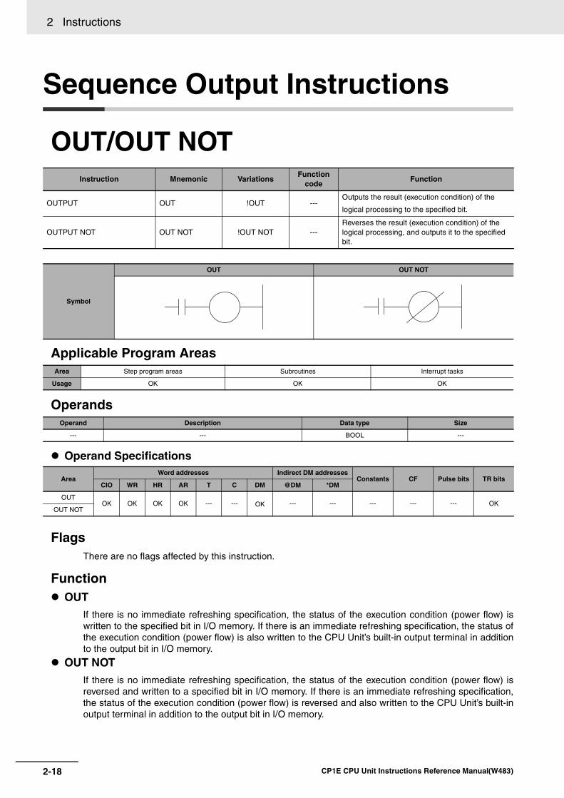
2 Instructions
Sequence Output Instructions
OUT/OUT NOT
Applicable Program Areas
Operands
Operand Specifications
FlagsThere are no flags affected by this instruction.
Function
Instruction Mnemonic VariationsFunction
codeFunction
OUTPUT OUT !OUT ---Outputs the result (execution condition) of the
logical processing to the specified bit.
OUTPUT NOT OUT NOT !OUT NOT ---Reverses the result (execution condition) of the logical processing, and outputs it to the specified bit.
Symbol
OUT OUT NOT
Area Step program areas Subroutines Interrupt tasks
Usage OK OK OK
Operand Description Data type Size
--- --- BOOL ---
Area Word addresses Indirect DM addresses
Constants CF Pulse bits TR bitsCIO WR HR AR T C DM @DM *DM
OUTOK OK OK OK --- --- OK --- --- --- --- --- OK
OUT NOT
OUTIf there is no immediate refreshing specification, the status of the execution condition (power flow) iswritten to the specified bit in I/O memory. If there is an immediate refreshing specification, the status ofthe execution condition (power flow) is also written to the CPU Unit’s built-in output terminal in additionto the output bit in I/O memory.
OUT NOTIf there is no immediate refreshing specification, the status of the execution condition (power flow) isreversed and written to a specified bit in I/O memory. If there is an immediate refreshing specification,the status of the execution condition (power flow) is reversed and also written to the CPU Unit’s built-inoutput terminal in addition to the output bit in I/O memory.
2-18 CP1E CPU Unit Instructions Reference Manual(W483)
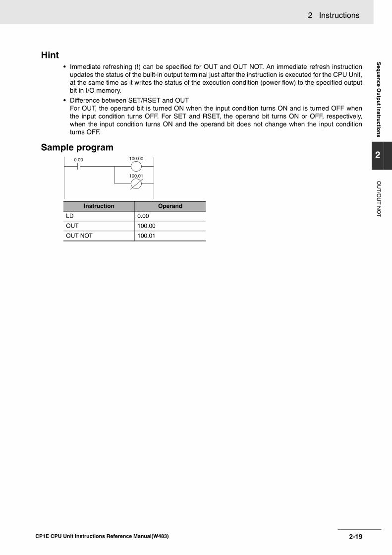
2 Instructions S
equ
ence O
utp
ut In
structio
ns
2
OU
T/O
UT
NO
T
Hint• Immediate refreshing (!) can be specified for OUT and OUT NOT. An immediate refresh instruction
updates the status of the built-in output terminal just after the instruction is executed for the CPU Unit,at the same time as it writes the status of the execution condition (power flow) to the specified outputbit in I/O memory.
• Difference between SET/RSET and OUT For OUT, the operand bit is turned ON when the input condition turns ON and is turned OFF whenthe input condition turns OFF. For SET and RSET, the operand bit turns ON or OFF, respectively,when the input condition turns ON and the operand bit does not change when the input conditionturns OFF.
Sample program
Instruction Operand
LD 0.00
OUT 100.00
OUT NOT 100.01
0.00 100.00
100.01
2-19CP1E CPU Unit Instructions Reference Manual(W483)

2 Instructions
TR
FunctionTR bits are used to temporarily retain the ON/OFF status of execution conditions in a program whenprogramming in mnemonic code. They are not used when programming directly in ladder program formbecause the processing is automatically executed by the Peripheral Device. The following diagramshows a simple application using two TR bits.
Instruction Mnemonic VariationsFunction
codeFunction
TR Bits TR --- ---TR bits are used to temporarily retain the ON/OFF status of execution conditions in a program when programming in mnemonic code.
Using TR0 to TR15• TR0 to TR15 are used only with LOAD and
OUTPUT instructions.
• There are no restrictions on the order inwhich the bit addresses are used.
• Sometimes it is possible to simplify a pro-gram by rewriting it so that TR bits are notrequired. The following diagram shows onecase in which a TR bit is unnecessary andone in which a TR bit is required.
In instruction block (1), the ON/OFF status atpoint A is the same as for output CIO 100.00,so AND 0.01 and OUT 100.01 can be codedwithout requiring a TR bit. In instruction block(2), the status of the branching point and thatof output CIO 100.02 are not necessarily thesame, so a TR bit must be used. In this case,the number of steps in the program could bereduced by using instruction block (1) in placeof instruction block (2).
LD 0.00
OUT
Coding
TR0
AND 0.01
OUT TR1
AND 0.02
OUT 100.00
LD TR1
AND 0.03
OUT 100.01
LD TR0
AND 0.04
OUT 100.02
LD TR0
AND NOT 100.00
OUT 100.03
Relay Address
TR0 to TR15Temporary Relay
Instruction Operands0.00 0.01 0.02
0.03
0.04
0.05
100.00
100.01
100.02
100.03
TR0 TR1
A0.00
0.01
0.02 0.03
(2)
100.00
100.01
100.02
100.03
TR0
(1)
2-20 CP1E CPU Unit Instructions Reference Manual(W483)

2 Instructions S
equ
ence O
utp
ut In
structio
ns
2
KE
EP
KEEP
Applicable Program Areas
Operands
Operand Specifications
FlagsNo flags are affected by KEEP(011).
Function
Instruction Mnemonic VariationsFunction
codeFunction
KEEP KEEP !KEEP 011 Operates like a latching relay.
Symbol
KEEP
Area Step program areas Subroutines Interrupt tasks
Usage OK OK OK
Operand Description Data type Size
R Bit BOOL ---
Area Word addresses Indirect DM addresses
Constants CF Pulse bits TR bitsCIO WR HR AR T C DM @DM *DM
R OK OK OK OK --- --- --- --- --- --- --- --- OK
When S turns ON, the designated bit will goON and stay ON until reset, regardless ofwhether S stays ON or goes OFF. When Rturns ON, the designated bit will go OFF. Therelationship between execution conditions andKEEP(011) bit status is shown below on theright.
KEEP(011)
R
S(SET)
R(RESET)R: Bit
ONOFF
ONOFF
ONOFF
Status of C
S execution condition
R execution condition
= CA
B
A
C
B
Set
Reset
KEEP
C
2-21CP1E CPU Unit Instructions Reference Manual(W483)

2 Instructions
Hint• KEEP(011) has an immediate refreshing variation (!KEEP(011)). When a CPU Unit built-in output bit
has been specified for R in a !KEEP(011) instruction, any changes to R will be refreshed when!KEEP(011) is executed and reflected immediately in the output bit.
• KEEP(011) operates like the self-maintaining bit, but a self-maintaining bit programmed withKEEP(011) requires one less instruction.
Self-maintaining bits programmed with KEEP(011) will maintain status even in an interlock programsection, unlike the self-maintaining bit programmed without KEEP(011).
• KEEP(011) can be used to create flip-flops as shown below.
0.02
0.03
KEEP
100.00
100.000.02
5.00
0.03
C
CA BA
B
KEEP
C
IL
ILC
IL
ILC
Output bit C will maintain its previous status in an interlock.
Output bit C will be turned OFF in an interlock.
A
A
B
B
KEEP
B
A
B
↑
↑
2-22 CP1E CPU Unit Instructions Reference Manual(W483)

2 Instructions S
equ
ence O
utp
ut In
structio
ns
2
KE
EP
• If a holding bit is used for R, the bit status will be retained even during a power interruption.KEEP(011) can thus be used to program bits that will maintain status after restarting the PLC follow-ing a power interruption. An example of this that can be used to produce a warning display followinga system shutdown for an emergency situation is shown below.
• The status of I/O Area bits can be retained in the event of a power interruption by turning ON the IOMHold Bit and setting IOM Hold Bit Hold in the PLC Setup. In this case, I/O Area bits used inKEEP(011) will maintain status after restarting the PLC following a power interruption, just like hold-ing bits. Be sure to restart the PLC after changing the PLC Setup; otherwise the new settings will notbe used.
Precautions
• If S and R are ON simultaneously, the resetinput takes precedence.
• The set input (S) cannot be received whileR is ON.
• Never use an input bit in a normally closedcondition on the reset (R) for KEEP(011)when the input device uses an AC powersupply. The delay in shutting down thePLC’s DC power supply (relative to the ACpower supply to the input device) can causethe operand bit of KEEP(011) to be reset.This situation is shown on the right.
0.02
0.03
0.04
0.05
H0.00
KEEP
H0.00
100.00
Reset input
Indicates emergency situation
Activates warning display
ONOFF
ONOFF
ONOFF
Set
Reset
Status of C
ONOFF
ONOFF
ONOFF
Set
Reset
Status of C
NEVER
S
RA
KEEPA
Input Unit
2-23CP1E CPU Unit Instructions Reference Manual(W483)
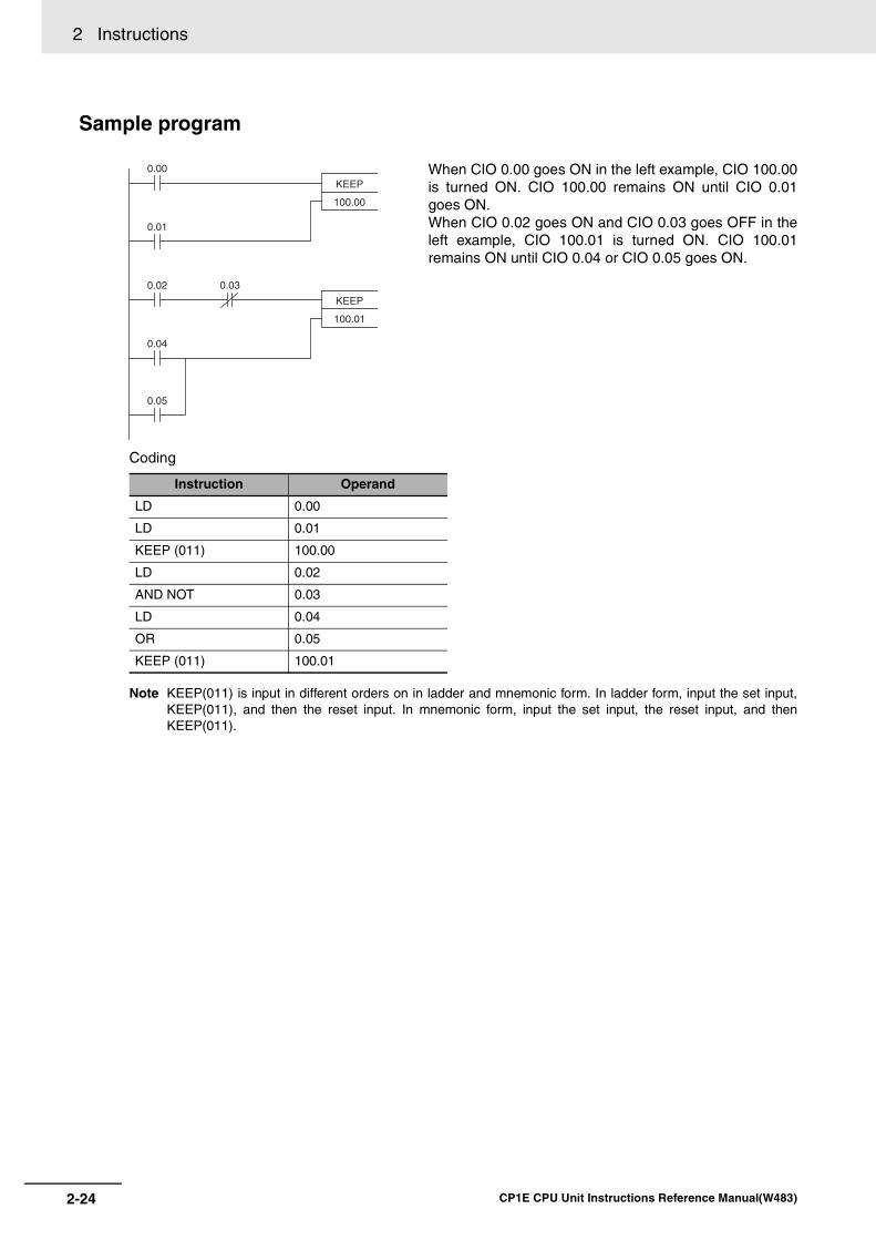
2 Instructions
Sample program
Coding
Note KEEP(011) is input in different orders on in ladder and mnemonic form. In ladder form, input the set input,KEEP(011), and then the reset input. In mnemonic form, input the set input, the reset input, and thenKEEP(011).
When CIO 0.00 goes ON in the left example, CIO 100.00is turned ON. CIO 100.00 remains ON until CIO 0.01goes ON.When CIO 0.02 goes ON and CIO 0.03 goes OFF in theleft example, CIO 100.01 is turned ON. CIO 100.01remains ON until CIO 0.04 or CIO 0.05 goes ON.
Instruction Operand
LD 0.00
LD 0.01
KEEP (011) 100.00
LD 0.02
AND NOT 0.03
LD 0.04
OR 0.05
KEEP (011) 100.01
0.00
0.01
KEEP
100.00
0.02 0.03
0.04
KEEP
100.01
0.05
2-24 CP1E CPU Unit Instructions Reference Manual(W483)

2 Instructions S
equ
ence O
utp
ut In
structio
ns
2
DIF
U
DIFU
Applicable Program Areas
Operands
Operand Specifications
FlagsNo flags are affected by DIFU(013).
Function
Hint
Instruction Mnemonic VariationsFunction
codeFunction
DIFFERENTIATE UP DIFU !DIFU 013DIFU(013) turns the designated bit ON for one cycle when the execution condition goes from OFF to ON (rising edge).
Symbol
DIFU
Area Step program areas Subroutines Interrupt tasks
Usage OK OK OK
Operand Description Data type Size
R Bit BOOL ---
Area Word addresses Indirect DM addresses
Constants CF Pulse bits TR bitsCIO WR HR AR T C DM @DM *DM
R OK OK OK OK --- --- --- --- --- --- --- --- ---
When the execution condition goes from OFFto ON, DIFU(013) turns R ON. WhenDIFU(013) is reached in the next cycle, R isturned OFF.
• UP(521) can be used to execute an instruction for just one cycle when the execution condition goesfrom OFF → ON.
• DIFU(013) has immediate refreshing variation (!DIFU(013)). When a CPU Unit built-in output bit hasbeen specified for R in this instruction, any changes to R will be refreshed when the instruction is exe-cuted and reflected immediately in the output bit.
DIFU(013)
R R: Bit
Status of R
Execution condition
1 cycle
2-25CP1E CPU Unit Instructions Reference Manual(W483)
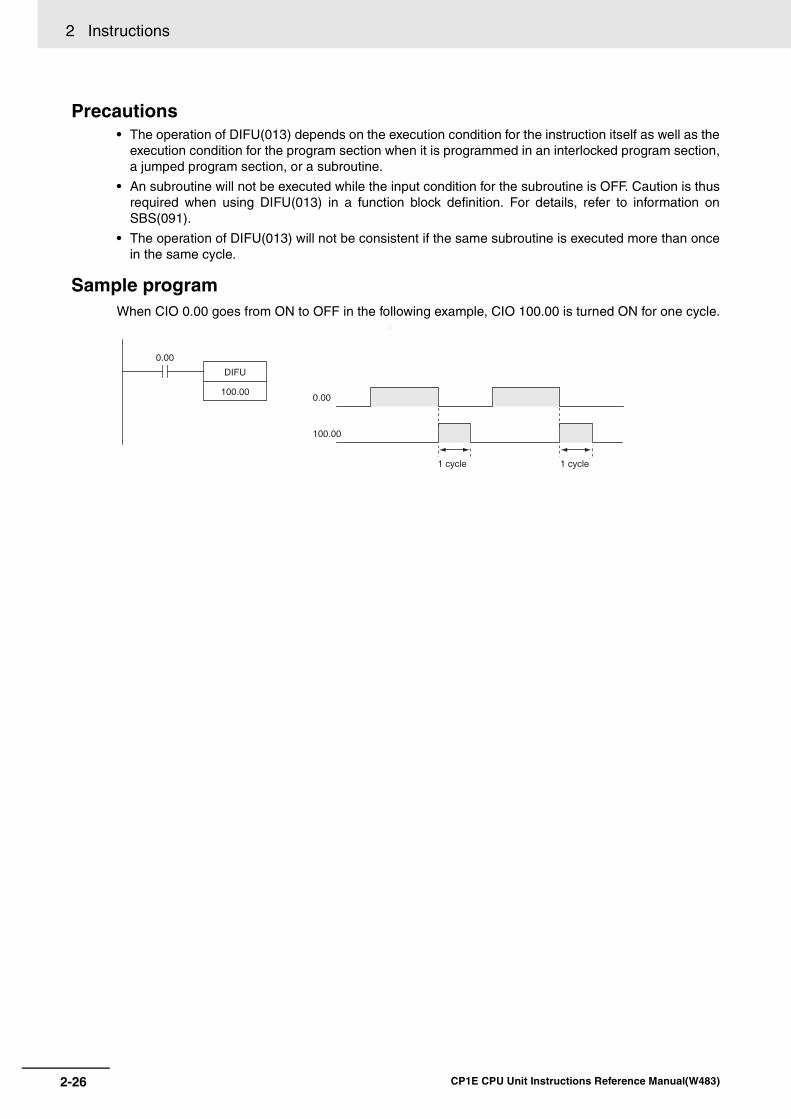
2 Instructions
Precautions• The operation of DIFU(013) depends on the execution condition for the instruction itself as well as the
execution condition for the program section when it is programmed in an interlocked program section,a jumped program section, or a subroutine.
• An subroutine will not be executed while the input condition for the subroutine is OFF. Caution is thusrequired when using DIFU(013) in a function block definition. For details, refer to information onSBS(091).
• The operation of DIFU(013) will not be consistent if the same subroutine is executed more than oncein the same cycle.
Sample programWhen CIO 0.00 goes from ON to OFF in the following example, CIO 100.00 is turned ON for one cycle.
i
DIFU
0.00
100.000.00
100.00
1 cycle 1 cycle
2-26 CP1E CPU Unit Instructions Reference Manual(W483)

2 Instructions S
equ
ence O
utp
ut In
structio
ns
2
DIF
D
DIFD
Applicable Program Areas
Operands
Operand Specifications
FlagsNo flags are affected by DIFD(014).
Function
Hint
Instruction Mnemonic VariationsFunction
codeFunction
DIFFERENTIATE DOWN DIFD !DIFD 014DIFD(014) turns the designated bit ON for one cycle when the execution condition goes from ON to OFF (falling edge).
Symbol
DIFD
Area Step program areas Subroutines Interrupt tasks
Usage OK OK OK
Operand Description Data type Size
R Bit BOOL ---
Area Word addresses Indirect DM addresses
Constants CF Pulse bits TR bitsCIO WR HR AR T C DM @DM *DM
B OK OK OK OK --- --- --- --- --- --- --- --- ---
When the execution condition goes from ONto OFF, DIFD(014) turns R ON. WhenDIFD(014) is reached in the next cycle, R isturned OFF.
• DOWN(522) can be used to execute an instruction for just one cycle when the execution condi-tion goes from ON → OFF.
• The operation of DIFD(014) depends on the execution condition for the instruction itself as wellas the execution condition for the program section when it is programmed in an interlocked pro-gram section, a jumped program section, or a subroutine.
• DIFD(014) has immediate refreshing variation (!DIFD(014)). When a CPU Unit built-in output bithas been specified for R in this instruction, any changes to R will be refreshed when the instruc-tion is executed and reflected immediately in the output bit.
DIFD(014)
R R: Bit
Status of R
1 cycle
Execution condition
2-27CP1E CPU Unit Instructions Reference Manual(W483)

2 Instructions
Precautions• The operation of DIFD(014) will not be consistent if the same function block instance is executed
more than once in the same cycle.
• An subroutine will not be executed while the input condition for the subroutine is OFF. Caution is thusrequired when using DIFD(014) in a function block definition. For details, refer to information onSBS(091).
Sample programWhen CIO 0.00 goes from ON to OFF in the following example, CIO 100.00 is turned ON for one cycle.
i
DIFD
0.00
100.00
0.00
100.00
1 cycle 1 cycle
2-28 CP1E CPU Unit Instructions Reference Manual(W483)

2 Instructions S
equ
ence O
utp
ut In
structio
ns
2
SE
T/R
SE
T
SET/RSET
Applicable Program Areas
Operands
Operand Specifications
FlagsNo flags are affected by SET and RSET.
Function
Instruction Mnemonic VariationsFunction
codeFunction
SET SET@SET, %SET, !SET, !@SET, !%SET
---
SET turns the operand bit ON when the execution condition is ON. After this, the specified contact will remain ON regardless of ON/OFF of the input condition.
RESET RSET@RSET, %RSET, !RSET, !@RSET, !%RSET
---
RSET turns the operand bit OFF when the execution condition is ON. After this, the specified contact will remain OFF regardless of ON/OFF of the input condition.
Symbol
SET RSET
Area Step program areas Subroutines Interrupt tasks
Usage OK OK OK
Operand Description Data type Size
R Bit BOOL ---
Area Word addresses Indirect DM addresses
Constants CF Pulse bits TR bitsCIO WR HR AR T C DM @DM *DM
R OK OK OK OK --- --- --- --- --- --- --- --- ---
SETSET turns the operand bit ON when the execution con-dition is ON, and does not affect the status of the oper-and bit when the execution condition is OFF. UseRSET to turn OFF a bit that has been turned ON withSET.
RSETRSET turns the operand bit OFF when the executioncondition is ON, and does not affect the status of theoperand bit when the execution condition is OFF. UseSET to turn ON a bit that has been turned OFF withRSET.
SET
R R: Bit
RSET
R R: Bit
ONOFF
ONOFF
Status of R
Execution condition of SET
ONOFF
ONOFFStatus of R
Execution condition of RSET
2-29CP1E CPU Unit Instructions Reference Manual(W483)

2 Instructions
Hint• Differences between OUT/OUT NOT and SET/RSET
The operation of SET differs from that of OUT because the OUT instruction turns the operand bitOFF when its execution condition is OFF. Likewise, RSET differs from OUT NOT because OUT NOTturns the operand bit ON when its execution condition is OFF. For OUT, the operand bit is turned ONwhen the input condition turns ON and is turned OFF when the input condition turns OFF. For SETand RSET, the operand bit turns ON or OFF, respectively, when the input condition turns ON and theoperand bit does not change when the input condition turns OFF.
• The set and reset inputs for a KEEP(011) instruction must be programmed with the instruction, butthe SET and RSET instructions can be programmed completely independently. Furthermore, thesame bit may be used as the operand in any number of SET or RSET instructions.
• SET and RSET have immediate refreshing variations (!SET and !RSET). When a CPU Unit built-inoutput bit has been specified for R in one of these instructions, any changes to R will be refreshedwhen the instruction is executed and reflected immediately in the output bit. If external output is specified for R by !SET (or !RSET), R will be OUT-refreshed as soon as it turnsON (or OFF) (when the instruction is executed). R, which turned ON (or OFF), will remain ON (orOFF) as normal until a RSET instruction (or SET instruction) is executed.
Precautions• SET and RSET cannot be used to set and reset timers and counters. When SET or RSET is pro-
grammed between IL(002) and ILC(003) or JMP(004) and JME(005), the status of the specified bitwill not be changed if the program section is interlocked or jumped.
0.01SET
100.00
0.02RSET
100.00
100.000.00CIO 100.00 is turned ON/OFF when CIO 0.00 goes ON/OFF.
CIO 100.00 is turned ON when CIO 0.01 goes ON; it remains ON until CIO 0.02 goes ON.
2-30 CP1E CPU Unit Instructions Reference Manual(W483)

2 Instructions S
equ
ence O
utp
ut In
structio
ns
2
SE
TA/R
STA
SETA/RSTA
Applicable Program Areas
Operands
Operand Specifications
Flags
Function
Instruction Mnemonic VariationsFunction
codeFunction
MULTIPLE BIT SET SETA @SETA 530SETA(530) turns ON the specified number of consecutive bits.
MULTIPLE BIT RESET RSTA @RSTA 531RSTA(531) turns OFF the specified number of consecutive bits.
Symbol
SETA RSTA
Area Step program areas Subroutines Interrupt tasks
Usage OK OK OK
Operand Description Data type Size
D Beginning Word UINT Variable
N1 Beginning Bit UINT 1
N2 Number of Bits UINT 1
Area Word addresses Indirect DM addresses
Constants CF Pulse bits TR bitsCIO WR HR AR T C DM @DM *DM
DOK OK OK OK OK OK OK OK OK
------ --- ---
N1,N2 OK
Operand Description Data type
Error Flag P_ER • ON if N1 is not within the specified range of 0000 to 000F (&0 to &15).
• OFF in all other cases.
SETASETA(530) turns ON N2 bits, beginningfrom bit N1 of D, and continuing to the left(more-significant bits). All other bits areleft unchanged. (No changes will bemade if N2 is set to 0.)
Bits turned ON by SETA(530) can beturned OFF by any other instructions, notjust RSTA(531).
SETA(530)
D
N1
N2
D: Beginning word
N1: Beginning bit
N2: Number of bits
RSTA(531)
D
N1
N2
D: Beginning word
N1: Beginning bit
N2: Number of bits
D
D+1
D+2
15 0
N1
1 1 1
1
1 1 1
N2 bits are set to 1 (ON).
2-31CP1E CPU Unit Instructions Reference Manual(W483)

2 Instructions
Hint SETA
• SETA(530) can be used to turn ON bits in data areas that are normally accessed by words only, suchas the DM areas.
RSTA• RSTA(531) can be used to turn OFF bits in data areas that are normally accessed by words only,
such as the DM areas.
Sample program SETA
When CIO 0.00 is turned ON in the following example, the 20 bits (0014 hexadecimal) beginningwith bit 5 of CIO 100 are turned ON.
RSTAWhen CIO 0.00 is turned ON in the following example, the 20 bits (0014 hexadecimal) beginningwith bit 3 of CIO 100 are turned OFF.
RSTARSTA(531) turns OFF N2 bits, beginningfrom bit N1 of D, and continuing to the left(more-significant bits). All other bits areleft unchanged. (No changes will bemade if N2 is set to 0.)
Bits turned OFF by RSTA(531) can beturned ON by any other instructions, notjust SETA(530).
D
D+1
D+2
15 0
N2 bits are reset to 0 (OFF).
N1
0 0 0
0
0 0 0
0.00
D
N1
N2
SETA
100
&5
&20
D: 100
101
15 1112 478 35 0
N2: 20 bits
N1: Bit 5
1
111111111
111111 1111
0.00
D
N1
N2
RSTA
100
&3
&20
D: 100
101
15 1112 478 3 0
0
0000000
00 000000 0000 N2: 20 bits
N1: Bit 3
2-32 CP1E CPU Unit Instructions Reference Manual(W483)
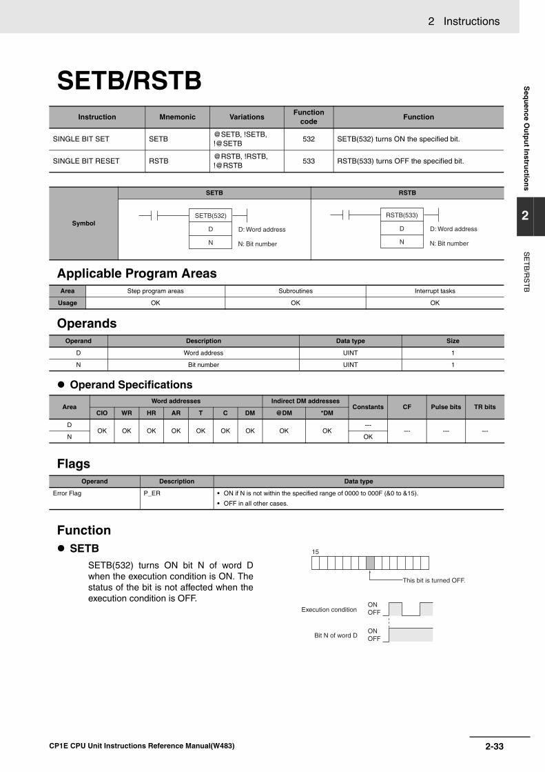
2 Instructions S
equ
ence O
utp
ut In
structio
ns
2
SE
TB
/RS
TB
SETB/RSTB
Applicable Program Areas
Operands
Operand Specifications
Flags
Function
Instruction Mnemonic VariationsFunction
codeFunction
SINGLE BIT SET SETB@SETB, !SETB, !@SETB
532 SETB(532) turns ON the specified bit.
SINGLE BIT RESET RSTB@RSTB, !RSTB, !@RSTB
533 RSTB(533) turns OFF the specified bit.
Symbol
SETB RSTB
Area Step program areas Subroutines Interrupt tasks
Usage OK OK OK
Operand Description Data type Size
D Word address UINT 1
N Bit number UINT 1
Area Word addresses Indirect DM addresses
Constants CF Pulse bits TR bitsCIO WR HR AR T C DM @DM *DM
DOK OK OK OK OK OK OK OK OK
------ --- ---
N OK
Operand Description Data type
Error Flag P_ER • ON if N is not within the specified range of 0000 to 000F (&0 to &15).
• OFF in all other cases.
SETBSETB(532) turns ON bit N of word Dwhen the execution condition is ON. Thestatus of the bit is not affected when theexecution condition is OFF.
D: Word address
SETB(532)
D
N N: Bit number
D: Word address
RSTB(533)
D
N N: Bit number
Execution conditionONOFF
Bit N of word DONOFF
15
This bit is turned OFF.
2-33CP1E CPU Unit Instructions Reference Manual(W483)

2 Instructions
Hint• Differences between SET/RSET and SETB(532)/RSTB(533)
The instructions operate in the same way when the specified bit is in the CIO, W, H, or A Area.The SETB(532) and RSTB(533) instructions can control bits in the DM Areas, unlike SET and RSET.
• The set and reset inputs for a KEEP(011) instruction must be programmed with the instruction, butthe SETB(532) and RSTB(533) instructions can be programmed completely independently. Further-more, the same bit may be used as the operand in any number of SETB(532) and RSTB(533)instructions.
Precautions• Bits turned ON by SETB(532) can be turned OFF by any other instruction, not just RSTB(533).
Bits turned OFF by RSTB(533) can be turned ON by any other instruction, not just SETB(532).
• SETB(532) and RSTB(533) cannot set/reset timers and counters.
• When SETB(532) or RSTB(533) is programmed between IL(002) and ILC(003) or JMP(004) andJME(005), the status of the specified bit will not be changed if the program section is interlocked orjumped, i.e., when the interlock condition or jump condition is OFF.
• SETB(532) and RSTB(533) have immediate refreshing variations (!SETB(532) and !RSTB(533)).When a CPU Unit built-in output bit has been specified in one of these instructions, any changes tothe specified bit will be refreshed when the instruction is executed and reflected immediately in theoutput bit.
• When a CPU Unit built-in output is specified for bit address N of word D by !SETB (or !RSTB instruc-tion), bit address N of word D which turned ON (or OFF) will be OUT-refreshed at that point (when theinstruction is executed). Bit address N of word D which was turned ON (or OFF) remains ON (orOFF) as normal until an RSTB instruction (or SETB instruction) is executed.
Sample program
RSTBRSTB(533) turns OFF bit N of word Dwhen the execution condition is ON. Thestatus of the bit is not affected when theexecution condition is OFF. (UseSETB(532) to turn ON the bit.)
Bit 02 of D0 is turned ON when CIO 0.00 is ON.
Bit 02 of D0 is turned OFF when CIO 0.01 is ON.
15
Execution conditionONOFF
Bit N of word DONOFF
This bit is turned OFF.
0.00
0.01
SETB
D0
&2
RSTB
D0
&2
2-34 CP1E CPU Unit Instructions Reference Manual(W483)

2 Instructions S
equ
ence C
on
trol In
structio
ns
2
Sequence Control Instructions
Overview of Interlock Instructions Interlock Instructions
The following instruction combinations can be used to interlock outputs in a program section.
• INTERLOCK and INTERLOCK CLEAR (IL(002) and IL(003))
• MULTI-INTERLOCK DIFFERENTIATION HOLD and MULTI-INTERLOCK CLEAR (MILH(517)and MILC(519))*
Note MILH(517) holds the status of the Differentiation Flag, so differentiated instructions that were interlocked areexecuted after the interlock is cleared.
• MULTI-INTERLOCK DIFFERENTIATION RELEASE and MULTI-INTERLOCK CLEAR (MILR(518)and MILC(519))*
Note MILR(518) does not hold the status of the Differentiation Flag, so differentiated instructions that were inter-locked are not executed after the interlock is cleared.
Differences between Interlocks and Multiple InterlocksRegular interlocks (IL(002) and IL(003)) cannot be nested, but multiple interlocks (MILH(517),MILR(518), and MILC(519)) can be nested. Ladder programming can be simplified by nesting multipleinterlocks, as shown in the following diagram.
aMILH
0
A1
bMILH
1
A2
cMILH
2
A3
MILC
2
MILC
1
MILC
0
aIL
A1
ILC
aIL
A2
b
b c
ILC
aIL
A3
ILC
Interlocks with MILH and MILC Interlocks with IL and ILC
2-35CP1E CPU Unit Instructions Reference Manual(W483)

2 Instructions
Differences between MILH(517) and MILR(518)Differentiated instructions (DIFU, DIFD, or instructions with a @ or % prefix) operate differently in inter-locks created with MILH(517) and MILR(518).
The operation of differentiated instructions in an interlock created with MILH(517) is identical to theoperation in an interlock created with IL(002).
For details, refer to MULTI-INTERLOCK DIFFERENTIATION HOLD, MULTI-INTERLOCK DIFFEREN-TIATION RELEASE, and MULTI-INTERLOCK CLEAR: MILH(517), MILR(518), and MILC(519).
PrecautionsDo not combine interlocks created with different interlock instructions (IL-ILC, MILH-MILC, and MILR-MILC). The interlocks may not operate properly if different interlock methods are used together. Fordetails on combining instructions, refer to MULTI-INTERLOCK DIFFERENTIATION HOLD, MULTI-INTERLOCK DIFFERENTIATION RELEASE, and MULTI-INTERLOCK CLEAR: MILH(517),MILR(518), and MILC(519).
For example, an MILH(517) instruction cannot be inserted between IL(002) and IL(003).
Note The different interlocks (IL-ILC, MILH-MILC, and MILR-MILC) can be used together as long as the inter-locked program sections do not overlap.
For example, all three interlock methods can be used without overlapping, as shown in the followingdiagram.
IL
MILH
ILC
MILH(517) is in an interlocked area between IL(002) and ILC.(003).
IL
MILH
MILC
ILC
MILR
MILC
Different interlock methods can be used as long as the interlocked areas do not overlap.
2-36 CP1E CPU Unit Instructions Reference Manual(W483)

2 Instructions S
equ
ence C
on
trol In
structio
ns
2
Differences between Interlocks and JumpsThe following table shows the differences between interlocks (created with IL(002)/ILC(003),MILH(517)/MILC(519), or MILR(518)/MILC(519)) and jumps created with JMP(004)/JME(005).
ItemTreatment in IL(002)/ILC(003),
MILH(517)/MILC (519), or MILR(518)/MILC (519)
Treatment inJMP(004)/JME(005)
Instruction execution Except OUT, OUT NOT, and timer instructions, all instructions are not executed.
No instructions are executed.
Output status in instructions Except for outputs in OUT, OUT NOT, and timer instructions, all outputs retain their previous status.
All outputs retain their previous status.
Bits in OUT, OUT NOT OFF All outputs retain their previous status.
Status of timer instructions(except (TTIM(087), TTIMX(555), MTIM(543), and MTIMX(554))
Reset Operating timers (TIM, TIMX(550), TIMH(015), TIMHX(551), TMHH(540), TMHHX(552) only) continue timing because the PVs are updated even when the timer instruction is not being executed.
2-37CP1E CPU Unit Instructions Reference Manual(W483)
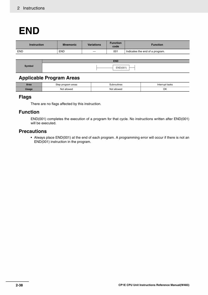
2 Instructions
END
Applicable Program Areas
FlagsThere are no flags affected by this instruction.
FunctionEND(001) completes the execution of a program for that cycle. No instructions written after END(001)will be executed.
Precautions• Always place END(001) at the end of each program. A programming error will occur if there is not an
END(001) instruction in the program.
Instruction Mnemonic VariationsFunction
codeFunction
END END --- 001 Indicates the end of a program.
Symbol
END
Area Step program areas Subroutines Interrupt tasks
Usage Not allowed Not allowed OK
END(001)
2-38 CP1E CPU Unit Instructions Reference Manual(W483)
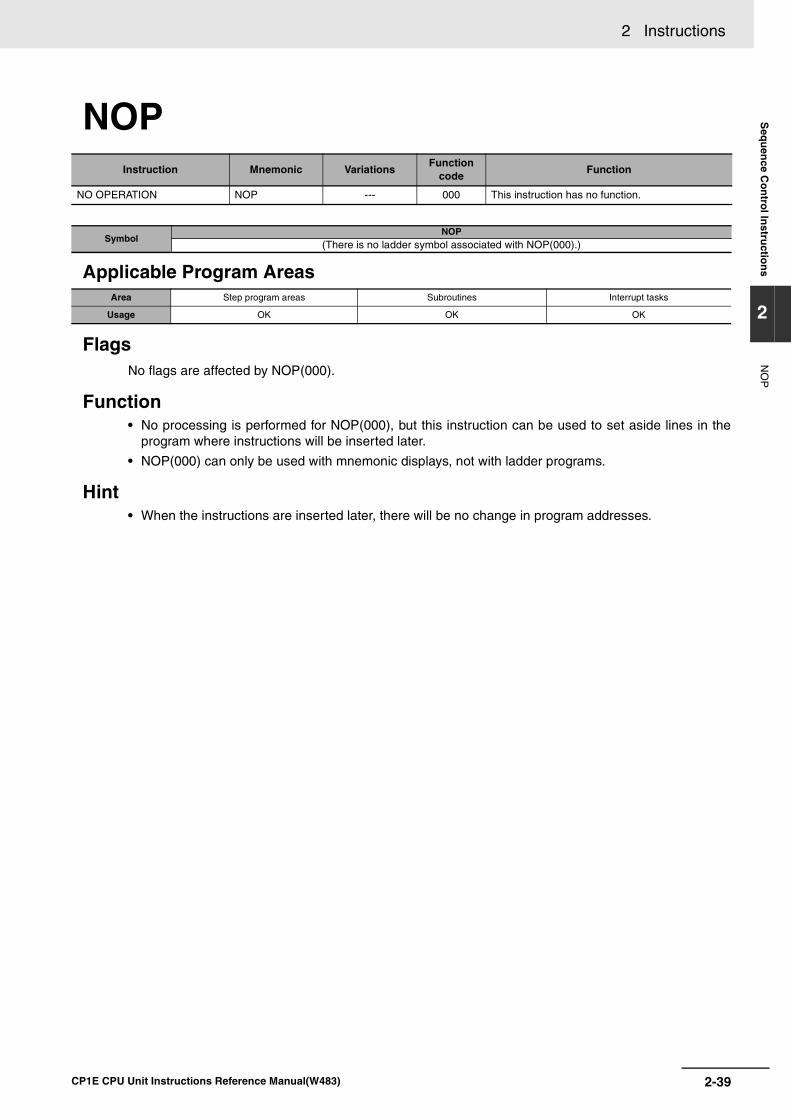
2 Instructions S
equ
ence C
on
trol In
structio
ns
2
NO
P
NOP
Applicable Program Areas
FlagsNo flags are affected by NOP(000).
Function• No processing is performed for NOP(000), but this instruction can be used to set aside lines in the
program where instructions will be inserted later.
• NOP(000) can only be used with mnemonic displays, not with ladder programs.
Hint• When the instructions are inserted later, there will be no change in program addresses.
Instruction Mnemonic VariationsFunction
codeFunction
NO OPERATION NOP --- 000 This instruction has no function.
SymbolNOP
(There is no ladder symbol associated with NOP(000).)
Area Step program areas Subroutines Interrupt tasks
Usage OK OK OK
2-39CP1E CPU Unit Instructions Reference Manual(W483)

2 Instructions
IL/ILC
Applicable Program Areas
FlagsThere are no flags affected by this instruction.
FunctionWhen the execution condition for IL(002) is OFF, the outputs for all instructions between IL(002) andILC(003) are interlocked. When the execution condition for IL(002) is ON, the instructions betweenIL(002) and ILC(003) are executed normally.
The following table shows the treatment of various outputs in an interlocked section between IL(002)and ILC(003).
Note Bits and words in all other instructions including TTIM(087), TTIMX(555), SET, RSET, CNT, CNTX(546),CNTR(012), CNTRX(548), SFT, and KEEP(011) retain their previous status.
Instruction Mnemonic VariationsFunction
codeFunction
INTERLOCK IL --- 002Interlocks all outputs between IL(002) and ILC(003) when the execution condition for IL(002) is OFF.
INTERLOCK CLEAR ILC --- 003 Indicates the end of the interlock range.
Symbol
IL ILC
Area Step program areas Subroutines Interrupt tasks
Usage Not allowed OK OK
Instruction Treatment
Bits specified in OUT, OUT NOT OFF
TIM, TIMX(550), TIMH(015), TIMHX(551), TMHH(540), TMHHX(552), TIML(542), and TIMXL(553)
Completion Flag OFF (reset)
PV Time set value (reset)
Bits/words specified in all other instructions (See note.) Retain previous status.
IL(002) ILC(003)
IL
ILC
Execution condition
Execution condition ON
Execution condition OFF
Interlocked section of the program
Normal Outputs execution interlocked.
2-40 CP1E CPU Unit Instructions Reference Manual(W483)

2 Instructions S
equ
ence C
on
trol In
structio
ns
2
IL/ILC
Hint
Precautions• The cycle time is not shortened when a section of the program is interlocked because the interlocked
instructions are executed internally.
• In general, IL(002) and ILC(003) are used in pairs, although it is possible to use more than oneIL(002) with a single ILC(003) as shown in the following diagram. If IL(002) and ILC(003) are notpaired, an error message will appear when the program check is performed but the program will beexecuted properly.
• IL(002) and ILC(003) cannot be nested, as in the following diagram. (Use MILH(517)/MILR(518) andMILC(519) when it is necessary to nest interlocks.)
• If there are bits which you want to remainON in an interlocked program section, setthese bits to ON with SET just beforeIL(002).
• It is often more efficient to switch a programsection with IL(002) and ILC(003). Whenseveral processes are controlled with thesame execution condition, it takes fewerprogram steps to put these processesbetween IL(002) and ILC(003).
IL
IL
AA
a
b
IL
IL
A
ILC
B
Executioncondition
Program section
a b A B
OFF ON Interlocked Interlocked
OFF OFF Interlocked Interlocked
ON OFF Not interlocked Interlocked
ON ON Not interlocked Not interlocked
IL
A
B
B
IL
ILC
ILC
2-41CP1E CPU Unit Instructions Reference Manual(W483)
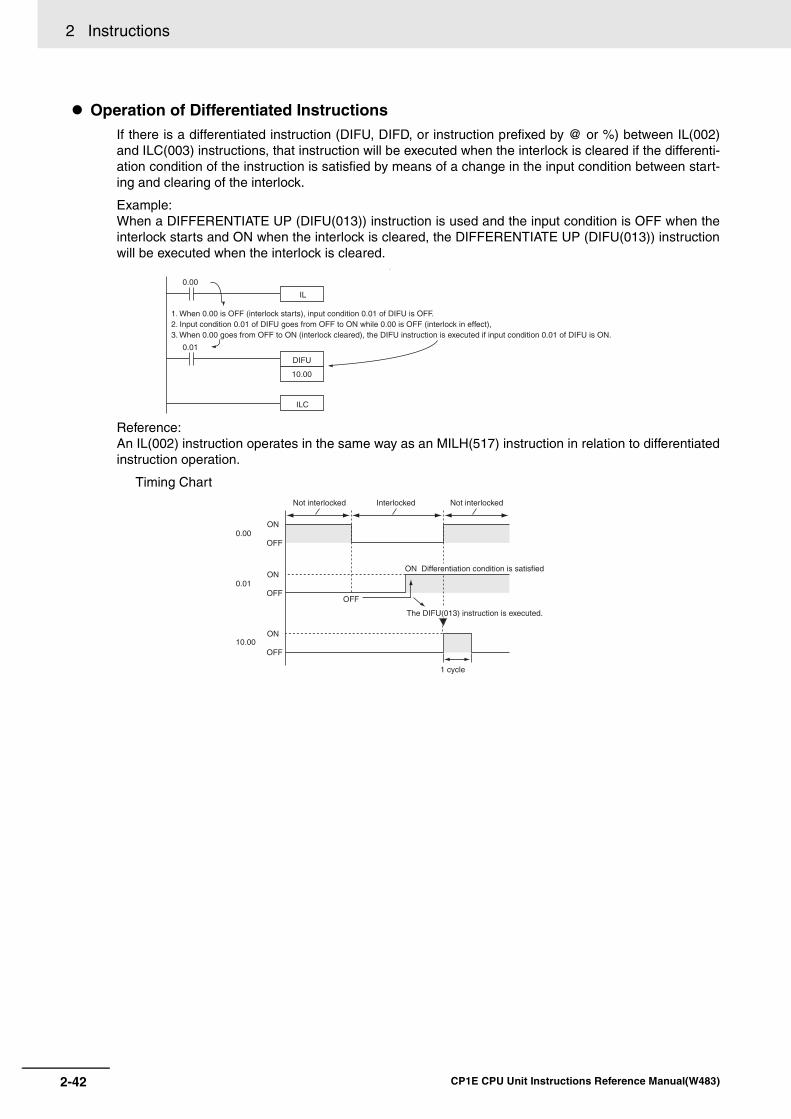
2 Instructions
Operation of Differentiated InstructionsIf there is a differentiated instruction (DIFU, DIFD, or instruction prefixed by @ or %) between IL(002)and ILC(003) instructions, that instruction will be executed when the interlock is cleared if the differenti-ation condition of the instruction is satisfied by means of a change in the input condition between start-ing and clearing of the interlock.
Example:When a DIFFERENTIATE UP (DIFU(013)) instruction is used and the input condition is OFF when theinterlock starts and ON when the interlock is cleared, the DIFFERENTIATE UP (DIFU(013)) instructionwill be executed when the interlock is cleared.
i
Reference:An IL(002) instruction operates in the same way as an MILH(517) instruction in relation to differentiatedinstruction operation.
Timing Chart
IL
ILC
DIFU
10.00
1. When 0.00 is OFF (interlock starts), input condition 0.01 of DIFU is OFF.2. Input condition 0.01 of DIFU goes from OFF to ON while 0.00 is OFF (interlock in effect),3. When 0.00 goes from OFF to ON (interlock cleared), the DIFU instruction is executed if input condition 0.01 of DIFU is ON.
0.00
0.01
1 cycle
The DIFU(013) instruction is executed.
Not interlocked Interlocked
ON0.00
0.01
10.00
OFF
OFF
ONON Differentiation condition is satisfied
OFF
ON
OFF
Not interlocked
2-42 CP1E CPU Unit Instructions Reference Manual(W483)

2 Instructions S
equ
ence C
on
trol In
structio
ns
2
IL/ILC
Sample programWhen CIO 0.00 is OFF in the rightexample, all outputs between IL(002)and ILC(003) are interlocked. WhenCIO 0.00 is ON in the right example,the instructions between IL(002) andILC(003) are executed normally.
IL
TIM
SET
0.03
CNT
ILC
0.00
0.01
0.02
2.00
H0
0.00 OFF
OFF
OFF
Reset
Retained
Retained
Normal execution
Outputs interlocked
0.00 ON
2-43CP1E CPU Unit Instructions Reference Manual(W483)

2 Instructions
MILH/MILR/MILC
Applicable Program Areas
Operands
N: Interlock NumberThe interlock number must be between 0 and 15. Match the interlock number of the MILH(517) (orMILR(518)) instruction with the same number in the corresponding MILC(519) instruction.The interlock numbers can be used in any order.
D: Interlock Status Bit• ON when the program section is not interlocked.
• OFF when the program section is interlocked.
When the interlock is engaged, the Interlock Status Bit can be force-set to release the interlock. Con-versely, when the interlock is not engaged, the Interlock Status Bit can be force-reset to engage theinterlock.
Operand Specifications
Flags
Instruction Mnemonic VariationsFunction
codeFunction
MULTI-INTERLOCK DIFFER-ENTIATION HOLD
MILH --- 517Interlocks all outputs between MILH(517) and MILC(519) when the execution condition for MILH(517) is OFF.
MULTI-INTERLOCK DIFFER-ENTIATION RELEASE
MILR --- 518Interlocks all outputs between MILR(518) and MILC(519) when the execution condition for MILR(518) is OFF.
MULTI-INTERLOCK CLEAR MILC --- 519Indicates the end of a multi-interlock range by means of an MILH or MILR instruction with the same interlock number.
Symbol
MILH MILR MILC
Area Step program areas Subroutines Interrupt tasks
Usage Not allowed OK OK
Operand Description Data type Size
N Interlock number -- 1
D Interlock status bit BOOL --
Area Word addresses Indirect DM addresses
Constants CF Pulse bits TR bitsCIO WR HR AR T C DM @DM *DM
N --- --- --- ------ --- --- --- ---
OK--- --- ---
D OK OK OK OK ---
Name Label Operation
Error Flag P_ER OFF
MILH(517)
N
D
N: Interlock Number
D: Interlock Status Bit
MILR(518)
N
D
N: Interlock Number
D: Interlock Status Bit
MILC(519)
N
N: Interlock Number
2-44 CP1E CPU Unit Instructions Reference Manual(W483)

2 Instructions S
equ
ence C
on
trol In
structio
ns
2
MILH
/MILR
/MILC
FunctionWhen the execution condition for MILH(517) (or MILR(518)) with interlock number N is OFF, the outputsfor all instructions between that MILH(517)/MILR(518) instruction and the next MILC(519) with interlocknumber N are interlocked.When the execution condition for MILH(517) (or MILR(518)) with interlock number N is ON, the instruc-tions between that MILH(517)/MILR(518) instruction and the next MILC(519) with interlock number Nare executed normally.
Interlock StatusThe following table shows the treatment of various outputs in an interlocked section betweenMILH(517)/MILR(518) instruction and the next MILC(519).
Note Bits and words in all other instructions including TTIM(087), TTIMX(555), SET, RSET, CNT, CNTX(546),CNTR(012), CNTRX(548), SFT, and KEEP(011) retain their previous status.
NestingInterlocks are nested when an interlocked program section (MILH(517)/MILR(518) and MILC(519) com-bination) is placed within another interlocked program section (MILH(517)/MILR(518) and MILC(519)combination). Interlocks can be nested up to 16 levels.Nesting can be used for the following kinds of applications.
Instruction Treatment
Bits specified in OUT, OUT NOT OFF
TIM, TIMX(550), TIMH(015), TIMHX(551), TMHH(540), TMHHX(552), TIML(542), and TIMXL(553)
Completion Flag OFF (reset)
PV Time set value (reset)
Bits/words specified in all other instructions (See note.) Retain previous status.
The MILH(517)/MILR(518) instruction turnsOFF the Interlock Status Bit (operand D)when the interlock is in engaged and turns ONthe bit when the interlock is not engaged.Consequently, the Interlock Status Bit can bemonitored to check whether or not the inter-lock for a given interlock number is engaged.
Example 1
Interlocking the entire program with one con-dition and interlocking a part of the programwith another condition (1 nesting level)
MILH
n
d
MILC
n
Input condition
Interlocked program section
Input condition ON (Normal operation) Input condition OFF
Normal operationInterlock Status Bit (d) ON
Outputs interlocked.(Outputs OFF, timers reset, etc.)Interlock Status Bit (d) OFF
Global interlock(Emergency stop)
A1 (Peripheral processing)
Partial interlock(Conveyor RUN)
A2 (Conveyor operation)
2-45CP1E CPU Unit Instructions Reference Manual(W483)

2 Instructions
• A1 and A2 are interlocked when theEmergency Stop Button is ON.
• A2 is interlocked when ConveyorRUN is OFF.
Example 2
Interlocking the entire program withone condition and interlocking twooverlapping parts of the program withother conditions (2 nesting levels)
• A1, A2, and A3 are interlockedwhen the Emergency Stop Button isON.
• A2 and A3 are interlocked whenConveyor RUN is OFF.
• A3 is interlocked when Arm RUN isOFF.
MILH
0
MILC
1
MILC
0
MILH
1
Global interlock(Emergency stop)
Partial interlock(Conveyor RUN)
A1 (Peripheral processing)
A2 (Conveyor operation)
When the Emergency Stop is ON (input condition OFF), both A1 and A2 are interlocked.When the Emergency Stop is OFF (input condition ON), A1 is executed normally and A2 is controlled by the Conveyor RUN switch as described below.
When the Conveyor RUN switch is OFF (input condition OFF), A2 is interlocked.When the Conveyor RUN switch is ON (input condition ON), A2 is executed normally.
Global interlock(Emergency stop)
A1 (Peripheral processing)
Partial interlock(Conveyor RUN)
A2 (Conveyor operation)
Partial interlock(Arm RUN)
A3 (Arm operation)
MILH
0
MILC
2
MILC
1
MILC
0
MILH
1
MILH
2
Global interlock(Emergency stop)
Partial interlock(Conveyor RUN)
A1 (Peripheral processing)
A2 (Conveyor operation)
Partial interlock(Arm RUN)
A3 (Arm operation)
When the Emergency Stop is ON (input condition OFF), A1, A2, and A3 are interlocked.When the Emergency Stop is OFF (input condition ON), A1 is executed normally and A2 and A3 are controlled by the Conveyor RUN and Arm RUN switches as described below.
When the Conveyor RUN switch is OFF (input condition OFF), both A2 and A3 are interlocked.When the Conveyor RUN switch is ON (input condition ON), A2 is executed normally and A3 is controlled by the Arm RUN switch as described below.
When the Arm RUN switch is OFF (input condition OFF), A3 is interlocked.When the Arm RUN switch is ON (input condition ON), A3 is executed normally.
2-46 CP1E CPU Unit Instructions Reference Manual(W483)

2 Instructions S
equ
ence C
on
trol In
structio
ns
2
MILH
/MILR
/MILC
Differences between MILH(517) and MILR(518)Differentiated instructions (DIFU, DIFD, or instructions with a @ or % prefix) operate differently in inter-locks created with MILH(517) and MILR(518).When a program section is interlocked with MILR(518), a differentiated instruction will not be executedwhen the interlock is cleared even if the differentiation condition was activated during the interlock(comparing the status of the execution condition when the interlock started to its status when the inter-lock was cleared).When a program section is interlocked with MILH(517), a differentiated instruction will be executedwhen the interlock is cleared if the differentiation condition was activated during the interlock (compar-ing the status of the execution condition when the interlock started to its status when the interlock wascleared).
Operation of Differentiated Instructions in an MILH(517) InterlockIf there is a differentiated instruction (DIFU, DIFD, or instruction with a @ or % prefix) betweenMILH(517) and the corresponding MILC(519), that instruction will be executed after the interlock iscleared if the differentiation condition of the instruction was established.In the same way, a differentiated instruction will be executed if its execution condition is established atthe same time that the interlock is started or cleared.Many other conditions in the program may cause the differentiation condition to be reset even if it wasestablished during the interlock. In this case, the differentiation instruction will not be executed when theinterlock is cleared.
ExampleWhen a DIFFERENTIATE UP (DIFU(013)) instruction is being used and the input condition is OFFwhen the interlock starts and ON when the interlock is cleared, DIFU(013) will be executed when theinterlock is cleared. (Differentiated instructions operate the same in the MILH(517) interlock as they
would in an IL(002) interlock.)
Instruction Operation of Differentiated Instructions
MILH(517)MULTI-INTERLOCK DIFFER-ENTIATION HOLD
A differentiated instruction (DIFU, DIFD, or instruction with a @ or % prefix) will be executed after the interlock is cleared if the differentiation condition of the instruction was established while the instruction was interlocked. (The status of the execution condition when the interlock started is compared to its status when the interlock was cleared.)
MILR(518)MULTI-INTERLOCK DIFFER-ENTIATION RELEASE
A differentiated instruction (DIFU, DIFD, or instruction with a @ or % prefix) will not be executed after the interlock is cleared even if the differentiation condition of the instruction was established while the instruction was interlocked.
Timing chart
MILH
0
MILC
0
DIFU
W0.0
0.00
0.01
1. When CIO 0.00 is OFF (interlock starts), the DIFU,s CIO 0.01 input condition is OFF.
2. The DIFU,s CIO 0.01 input condition goes from OFF to ON while CIO 0.00 is OFF (DIFU interlocked),
3. When CIO 0.00 goes from OFF to ON (interlock cleared), DIFU is executed if CIO 0.01 is still ON.
ON0.00
0.01
W0.0
OFF
OFF
ONON
OFF
ON
OFF
1 cycle
DIFU(013) is executed.MILH(517) interlock
Not interlocked Interlocked Not interlocked
Status (OFF) at start of interlock Differentiation condition established
Status (ON) when interlock is cleared
2-47CP1E CPU Unit Instructions Reference Manual(W483)

2 Instructions
Operation of Differentiated Instructions in an MILR(518) InterlockIf there is a differentiated instruction (DIFU, DIFD, or instruction with a @ or % prefix) betweenMILR(518) and the corresponding MILC(519), that instruction will not be executed after the interlock iscleared even if the differentiation condition of the instruction was established.In the same way, a differentiated instruction will not be executed if its execution condition is establishedat the same time that the interlock is started or cleared.
ExampleWhen a DIFFERENTIATE UP (DIFU(013)) instruction is being used and the input condition is OFFwhen the interlock starts and ON when the interlock is cleared, DIFU(013) will not be executed when
the interlock is cleared.
Controlling Interlock Status from a Programming DeviceAn interlock can be engaged or released manually by force-resetting or force-setting the Interlock Sta-tus Bit (specified with operand D of MILH(517) and MILR(518)) from a Programming Device. The forcedstatus of the Interlock Status Bit has priority and overrides the interlock status calculated by program
execution.
Timing chart
Force-set: Releases the interlock. Force-reset: Engages the interlock.
MILR
0
MILC
0
DIFU
W0.0
0.00
0.01
1. When CIO 0.00 is OFF (interlock starts), the DIFU,s CIO 0.01 input condition is OFF.
2. The DIFU,s CIO 0.01 input condition goes from OFF to ON while CIO 0.00 is OFF (DIFU interlocked),
3. When CIO 0.00 goes from OFF to ON (interlock cleared), DIFU is not executed even though CIO 0.01 is still ON.
ON0.00
0.01
W0.0
OFF
OFF
ONON
OFF
ON
OFF
DIFU(013) is not executed.MILR(518) interlock
Not interlocked Interlocked Not interlocked
OFF
MILC
n
MILH
n
100.00
If CIO 100.00 is force-set (ON), the interlock is released.
CIO 100.00 is OFF when the interlock is engaged.
Program section controlled by interlock
MILC
n
ONMILH
n
100.00
If CIO 100.00 is force-reset (OFF), the interlock is engaged.
CIO 100.00 is ON when the interlock is not engaged.
Program section controlled by interlock
2-48 CP1E CPU Unit Instructions Reference Manual(W483)

2 Instructions S
equ
ence C
on
trol In
structio
ns
2
MILH
/MILR
/MILC
Hint• The cycle time is not shortened when a section of the program is interlocked by MILH(517) or
MILR(518) because the interlocked instructions are executed internally.
• When nesting interlocks, assign interlock numbers so that the nested program section does not
exceed the outer program section.
• Other instructions can be input betweenthe MILC(519) instructions, as shown inthe following diagram.
• If there is an ILC(003) instruction betweenan MILH(517) and MILC(519) pair, the pro-gram section between MILH(517) andILC(003) will be interlocked.
a
b
MILH
0
MILC
0
MILC
1
A1
MILH
1
A2
A3
The nested program section must not go beyond the outer program section.
Execution condition
Program section
a b A1 A2 A3
OFF ON Interlocked Interlocked Interlocked
OFF
ON OFF Not interlocked Interlocked Interlocked
ON Not interlocked Not interlocked Not interlocked
a
b
MILH
0
100.00
MILC
1
MILC
0
A1
MILH
1
100.01
A2
A3
Other instructions can be inserted between two MILC(519) instructions. In this case, sections A1 and A3 operate together. (They are interlocked when “a” is OFF, regardless of the ON/OFF status of “b”.)
aMILH
0
MILC
0
A1
ILC
A2
The MILC(519) instruction is ignored.
When input condition “a” is OFF, only program section A1 is interlocked.
If there is an ILC(003) instruction, the interlock is cleared at that point.
2-49CP1E CPU Unit Instructions Reference Manual(W483)
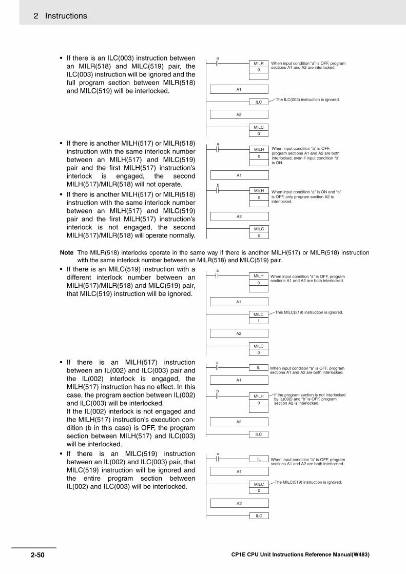
2 Instructions
• If there is an ILC(003) instruction betweenan MILR(518) and MILC(519) pair, theILC(003) instruction will be ignored and thefull program section between MILR(518)and MILC(519) will be interlocked.
• If there is another MILH(517) or MILR(518)instruction with the same interlock numberbetween an MILH(517) and MILC(519)pair and the first MILH(517) instruction’sinterlock is engaged, the secondMILH(517)/MILR(518) will not operate.
• If there is another MILH(517) or MILR(518)instruction with the same interlock numberbetween an MILH(517) and MILC(519)pair and the first MILH(517) instruction’sinterlock is not engaged, the secondMILH(517)/MILR(518) will operate normally.
Note The MILR(518) interlocks operate in the same way if there is another MILH(517) or MILR(518) instructionwith the same interlock number between an MILR(518) and MILC(519) pair.
• If there is an MILC(519) instruction with adifferent interlock number between anMILH(517)/MILR(518) and MILC(519) pair,that MILC(519) instruction will be ignored.
• If there is an MILH(517) instructionbetween an IL(002) and ILC(003) pair andthe IL(002) interlock is engaged, theMILH(517) instruction has no effect. In thiscase, the program section between IL(002)and ILC(003) will be interlocked.If the IL(002) interlock is not engaged andthe MILH(517) instruction’s execution con-dition (b in this case) is OFF, the programsection between MILH(517) and ILC(003)will be interlocked.
• If there is an MILC(519) instructionbetween an IL(002) and ILC(003) pair, thatMILC(519) instruction will be ignored andthe entire program section betweenIL(002) and ILC(003) will be interlocked.
aMILR
0
MILC
0
A1
ILC
A2
The ILC(003) instruction is ignored.
When input condition “a” is OFF, program sections A1 and A2 are interlocked.
aMILH
0
MILC
0
A1
bMILH
0
A2
When input condition “a” is OFF, program sections A1 and A2 are both interlocked, even if input condition “b” is ON.
When input condition “a” is ON and “b” is OFF, only program section A2 is interlocked.
aMILH
0
MILC
0
A1
MILC
1
A2
This MILC(519) instruction is ignored.
When input condition “a” is OFF, program sections A1 and A2 are both interlocked.
a
b
IL
ILC
A1
MILH
0
A2
When input condition “a” is OFF, program sections A1 and A2 are both interlocked.
If the program section is not interlocked by IL(002) and “b” is OFF, program section A2 is interlocked.
a
IL
ILC
A1
MILC
0
A2
The MILC(519) instruction is ignored.
When input condition “a” is OFF, program sections A1 and A2 are both interlocked.
2-50 CP1E CPU Unit Instructions Reference Manual(W483)
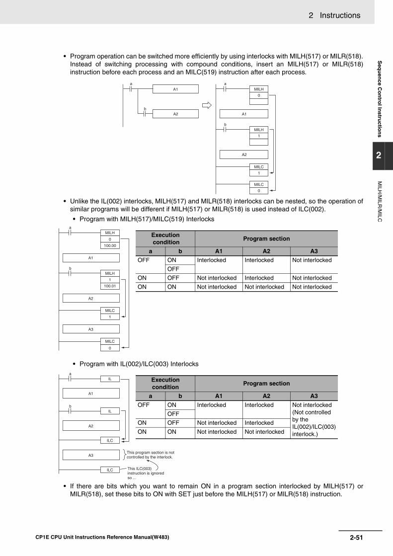
2 Instructions S
equ
ence C
on
trol In
structio
ns
2
MILH
/MILR
/MILC
• Program operation can be switched more efficiently by using interlocks with MILH(517) or MILR(518).Instead of switching processing with compound conditions, insert an MILH(517) or MILR(518)instruction before each process and an MILC(519) instruction after each process.
• Unlike the IL(002) interlocks, MILH(517) and MILR(518) interlocks can be nested, so the operation ofsimilar programs will be different if MILH(517) or MILR(518) is used instead of ILC(002).
• Program with MILH(517)/MILC(519) Interlocks
• Program with IL(002)/ILC(003) Interlocks
• If there are bits which you want to remain ON in a program section interlocked by MILH(517) orMILR(518), set these bits to ON with SET just before the MILH(517) or MILR(518) instruction.
a
b
aMILH
0
MILC
1
MILC
0
A1
A1
b
MILH
1
A2
A2
a
b
MILH
0
100.00
MILC
1
MILC
0
A1
MILH
1
100.01
A2
A3
Execution condition
Program section
a b A1 A2 A3
OFF ON Interlocked Interlocked Not interlocked
OFF
ON OFF Not interlocked Interlocked Not interlocked
ON ON Not interlocked Not interlocked Not interlocked
a
b
IL
ILC
ILC
A1
IL
A2
A3This program section is not controlled by the interlock.
This ILC(003) instruction is ignored so ...
Execution condition
Program section
a b A1 A2 A3
OFF ON Interlocked Interlocked Not interlocked(Not controlled by the IL(002)/ILC(003) interlock.)
OFF
ON OFF Not interlocked Interlocked
ON ON Not interlocked Not interlocked
2-51CP1E CPU Unit Instructions Reference Manual(W483)

2 Instructions
Sample programWhen W0.00 and W0.01 are both ON, the instructions between MILH(517) with interlock number 0 andMILC(519) with interlock number 0 are executed normally.
When W0.00 is OFF, the instructions between MILH(517) with interlock number 0 and MILC(519) withinterlock number 0 are interlocked.
When W0.00 is ON and W0.01 are OFF, the instructions between MILH(517) with interlock number 1and MILC(519) with interlock number 1 are interlocked. The other instructions are executed normally.
i
W0.00
0.01
0.02
2.00
H0
OFF
OFF
W0.00 OFF
MILH
0
100.00
W0.01MILH
1
100.01
CNT
1
#0010
SET
0.03
MILC
1
MILC
0
W0.00 and W0.01 both ON
W0.00 ON and W0.01 OFF
Executed normally.
Executed normally.
Outputs interlocked. Outputs
interlocked.Held
Held Executed normally.
2-52 CP1E CPU Unit Instructions Reference Manual(W483)
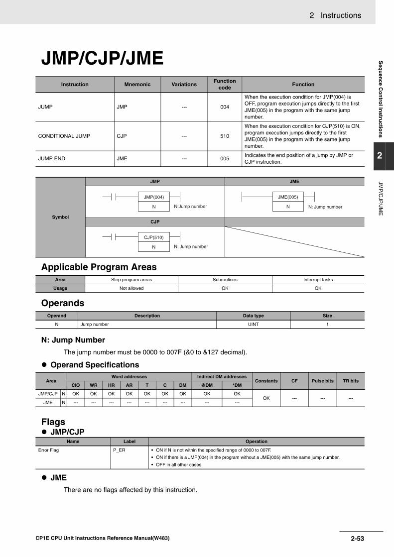
2 Instructions S
equ
ence C
on
trol In
structio
ns
2
JMP
/CJP
/JME
JMP/CJP/JME
Applicable Program Areas
Operands
N: Jump NumberThe jump number must be 0000 to 007F (&0 to &127 decimal).
Operand Specifications
Flags JMP/CJP
JMEThere are no flags affected by this instruction.
Instruction Mnemonic VariationsFunction
codeFunction
JUMP JMP --- 004
When the execution condition for JMP(004) is OFF, program execution jumps directly to the first JME(005) in the program with the same jump number.
CONDITIONAL JUMP CJP --- 510
When the execution condition for CJP(510) is ON, program execution jumps directly to the first JME(005) in the program with the same jump number.
JUMP END JME --- 005Indicates the end position of a jump by JMP or CJP instruction.
Symbol
JMP JME
CJP
Area Step program areas Subroutines Interrupt tasks
Usage Not allowed OK OK
Operand Description Data type Size
N Jump number UINT 1
Area Word addresses Indirect DM addresses
Constants CF Pulse bits TR bitsCIO WR HR AR T C DM @DM *DM
JMP/CJP N OK OK OK OK OK OK OK OK OKOK --- --- ---
JME N --- --- --- --- --- --- --- --- ---
Name Label Operation
Error Flag P_ER • ON if N is not within the specified range of 0000 to 007F.
• ON if there is a JMP(004) in the program without a JME(005) with the same jump number.
• OFF in all other cases.
JMP(004)
N N:Jump number N: Jump number
JME(005)
N
CJP(510)
N N: Jump number
2-53CP1E CPU Unit Instructions Reference Manual(W483)
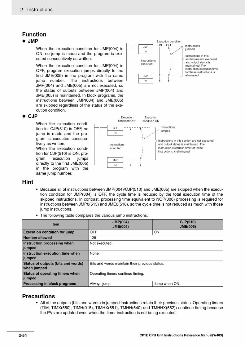
2 Instructions
Function
Hint• Because all of instructions between JMP(004)/CJP(510) and JME(005) are skipped when the execu-
tion condition for JMP(004) is OFF, the cycle time is reduced by the total execution time of theskipped instructions. In contrast, processing time equivalent to NOP(000) processing is required forinstructions between JMP0(515) and JME0(516), so the cycle time is not reduced as much with thosejump instructions.
• The following table compares the various jump instructions.
Precautions
JMPWhen the execution condition for JMP(004) isON, no jump is made and the program is exe-cuted consecutively as written.
When the execution condition for JMP(004) isOFF, program execution jumps directly to thefirst JME(005) in the program with the samejump number. The instructions betweenJMP(004) and JME(005) are not executed, sothe status of outputs between JMP(004) andJME(005) is maintained. In block programs, theinstructions between JMP(004) and JME(005)are skipped regardless of the status of the exe-cution condition.
CJPWhen the execution condi-tion for CJP(510) is OFF, nojump is made and the pro-gram is executed consecu-tively as written.When the execution condi-tion for CJP(510) is ON, pro-gram execution jumpsdirectly to the first JME(005)in the program with thesame jump number.
ItemJMP(004)JME(005)
CJP(510)JME(005)
Execution condition for jump OFF ON
Number allowed 128
Instruction processing when jumped
Not executed.
Instruction execution time when jumped
None
Status of outputs (bits and words) when jumped
Bits and words maintain their previous status.
Status of operating timers when jumped
Operating timers continue timing.
Processing in block programs Always jump. Jump when ON.
• All of the outputs (bits and words) in jumped instructions retain their previous status. Operating timers(TIM, TIMX(550), TIMH(015), TIMHX(551), TMHH(540) and TMHHX(552)) continue timing becausethe PVs are updated even when the timer instruction is not being executed.
Instructions in this section are not executed and output status is maintained. The instruction execution time for these instructions is eliminated.
Instructions jumped
Execution conditionON OFF
Instructions executed
JMP
N
JME
N
Instructions in this section are not executed and output status is maintained. The instruction execution time for these instructions is eliminated.
Instructions jumped
Execution condition ON
Execution condition OFF
Instructions executed
CJP
N
JME
N
2-54 CP1E CPU Unit Instructions Reference Manual(W483)
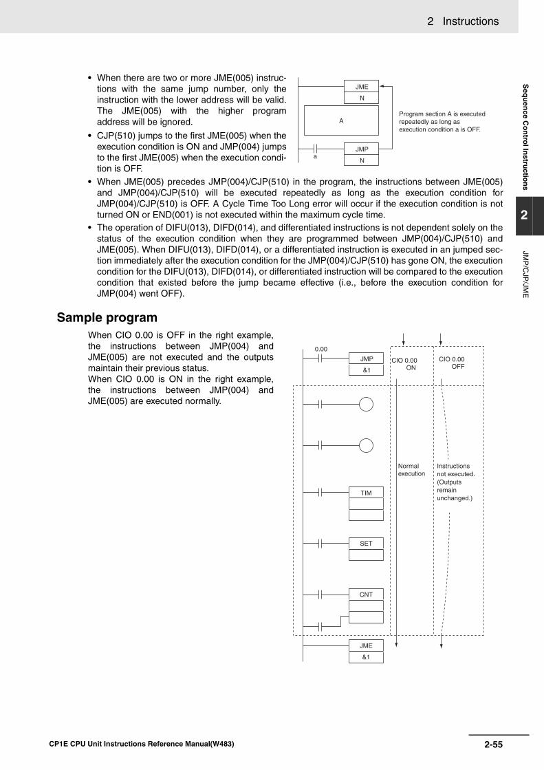
2 Instructions S
equ
ence C
on
trol In
structio
ns
2
JMP
/CJP
/JME
Sample program
• When there are two or more JME(005) instruc-tions with the same jump number, only theinstruction with the lower address will be valid.The JME(005) with the higher programaddress will be ignored.
• CJP(510) jumps to the first JME(005) when theexecution condition is ON and JMP(004) jumpsto the first JME(005) when the execution condi-tion is OFF.
• When JME(005) precedes JMP(004)/CJP(510) in the program, the instructions between JME(005)and JMP(004)/CJP(510) will be executed repeatedly as long as the execution condition forJMP(004)/CJP(510) is OFF. A Cycle Time Too Long error will occur if the execution condition is notturned ON or END(001) is not executed within the maximum cycle time.
• The operation of DIFU(013), DIFD(014), and differentiated instructions is not dependent solely on thestatus of the execution condition when they are programmed between JMP(004)/CJP(510) andJME(005). When DIFU(013), DIFD(014), or a differentiated instruction is executed in an jumped sec-tion immediately after the execution condition for the JMP(004)/CJP(510) has gone ON, the executioncondition for the DIFU(013), DIFD(014), or differentiated instruction will be compared to the executioncondition that existed before the jump became effective (i.e., before the execution condition forJMP(004) went OFF).
When CIO 0.00 is OFF in the right example,the instructions between JMP(004) andJME(005) are not executed and the outputsmaintain their previous status.When CIO 0.00 is ON in the right example,the instructions between JMP(004) andJME(005) are executed normally.
Program section A is executed repeatedly as long as execution condition a is OFF.
a
A
JMP
N
JME
N
CIO 0.00ON
CIO 0.00OFF&1
0.00
TIM
SET
CNT
JME
&1
JMP
&1
Normal execution
Instructions not executed. (Outputs remain unchanged.)
2-55CP1E CPU Unit Instructions Reference Manual(W483)

2 Instructions
FOR/NEXT
Applicable Program Areas
Operands
N: Number of loopsThe number of loops must be 0000 to FFFF (0 to 65,535 decimal).
Operand Specifications
Flags
Function
Instruction Mnemonic VariationsFunction
codeFunction
---FOR --- 512 The instructions between FOR(512) and
NEXT(513) are repeated a specified number of times.NEXT --- 513
Symbol
FOR NEXT
Area Step program areas Subroutines Interrupt tasks
Usage --- OK OK
Operand Description Data type Size
N Number of loops UINT 1
Area Word addresses Indirect DM addresses
Constants CF Pulse bits TR bitsCIO WR HR AR T C DM @DM *DM
N OK OK OK OK OK OK OK OK OK OK --- --- ---
Name Label Operation
Error Flag P_ER • ON if more than 15 loops are nested.
• OFF in all other cases.
Equals Flag P_EQ OFF
Negative Flag P_N OFF
The instructions between FOR(512) and NEXT(513)are executed N times and then program execution con-tinues with the instruction after NEXT(513). TheBREAK(514) instruction can be used to cancel theloop.If N is set to 0, the instructions between FOR(512) andNEXT(513) are processed as NOP(000) instructions.Loops can be used to process tables of data with aminimum amount of programming.
FOR(512)
N N: Number of loops
NEXT(513)
Repeated N times
Repeated program section
NEXT
FOR
N
2-56 CP1E CPU Unit Instructions Reference Manual(W483)

2 Instructions S
equ
ence C
on
trol In
structio
ns
2
FO
R/N
EX
T
HintThere are two ways to repeat a program section until a given execution condition is input.
• FOR-NEXT Loop with BREAKStart a FOR-NEXT loop with a maximum of N repetitions. Program BREAK(514) within the loop withthe desired execution condition. The loop will end before N repetitions if the execution condition isinput.
• JME(005)-JMP(004) LoopProgram a loop with JME(005) before JMP(004). The instructions between JME(005) and JMP(004)will be executed repeatedly as long as the execution condition for JMP(004) is OFF. (A Cycle TimeToo Long error will occur if the execution condition is not turned ON or END(001) is not executedwithin the maximum cycle time.)
Precautions• Program FOR(512) and NEXT(513) in the same task. Execution will not be repeated if these instruc-
tions are not in the same task.
• If a loop repeats in one cycle and a differentiated instruction is used in the FOR-NEXT loop, thatinstruction will be executed only once.It is not executed the number of loops.
• UP(521),DOWN(522)
• DIFU(013),DIFD(014)
• Differentiated up instruction(Differentiation variation:@)
• Differentiated down instruction(Differentiation variation:%)
• FOR-NEXT loops can be nested up to 15 levels.
In the example above, program sections A, B, and C are executed as follows:A → B → B → C, A → B → B → C, and A → B → B → C
• Use BREAK(514) to escape from a FOR-NEXT loop. Several BREAK(514) instructions (the numberof levels nested) are required to escape from nested loops.
• The remaining instructions in the loop after BREAK(514) are processed as NOP(000) instructions.
A
FOR
&3
B
FOR
&2
C
NEXT
NEXT
2-57CP1E CPU Unit Instructions Reference Manual(W483)
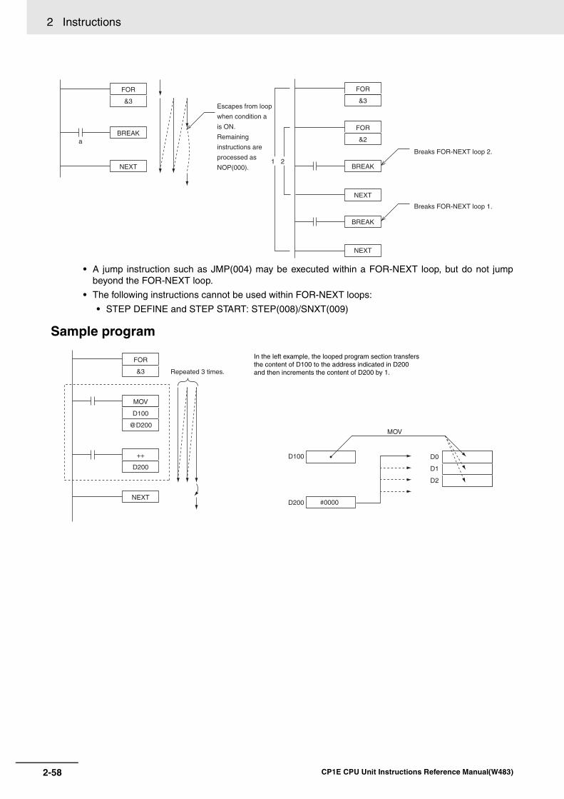
2 Instructions
• A jump instruction such as JMP(004) may be executed within a FOR-NEXT loop, but do not jumpbeyond the FOR-NEXT loop.
• The following instructions cannot be used within FOR-NEXT loops:
• STEP DEFINE and STEP START: STEP(008)/SNXT(009)
Sample program
&3
Breaks FOR-NEXT loop 2.
Breaks FOR-NEXT loop 1.
Escapes from loop
when condition a
is ON.
Remaining
instructions are
processed as
NOP(000).
FOR
&3
BREAK
NEXT
a
FOR
&2
BREAK
NEXT
FOR
&3
BREAK
NEXT
21
#0000
D100 D0
D1
D2
D200
Repeated 3 times.
In the left example, the looped program section transfers the content of D100 to the address indicated in D200 and then increments the content of D200 by 1.
FOR
&3
MOV
D100
@D200
++
D200
NEXT
MOV
#0000
2-58 CP1E CPU Unit Instructions Reference Manual(W483)

2 Instructions S
equ
ence C
on
trol In
structio
ns
2
BR
EA
K
BREAK
Applicable Program Areas
Flags
Function
Precautions• A BREAK(514) instruction cancels only one loop, so several BREAK(514) instructions (the number of
levels nested) are required to escape from nested loops.
• BREAK(514) can be used only in a FOR-NEXT loop.
Instruction Mnemonic VariationsFunction
codeFunction
BREAK LOOP BREAK --- 514
Programmed in a FOR-NEXT loop to cancel the execution of the loop for a given execution condi-tion. The remaining instructions in the loop are processed as NOP(000) instructions.
Symbol
BREAK
Area Step program areas Subroutines Interrupt tasks
Usage --- OK OK
Name Label Operation
Error Flag P_ER OFF
Equals Flag P_EQ OFF
Negative Flag P_N OFF
Program BREAK(514) between FOR(512) andNEXT(513) to cancel the FOR-NEXT loopwhen BREAK(514) is executed. WhenBREAK(514) is executed, the rest of theinstructions up to NEXT(513) are processed asNOP(000).
BREAK(514)
N repetitionsCondition a ON
Processed as NOP(000).
Repetitions forced to end.
FOR
N
BREAK
NEXT
a
2-59CP1E CPU Unit Instructions Reference Manual(W483)

2 Instructions
Timer and Counter Instructions
Refresh Methods for Timer/Counter PV Overview
There are two PV refresh methods for instructions related to timer/counters, “BCD” and “BINARY”.
The PLC Setup for all of the timer/counter-related instructions. The refresh method is valid also whensetting an SV indirectly (i.e., using the contents of memory word). (That is, the contents of theaddressed word is taken as either BCD or binary data according to the refresh method that is set.)
Applicable Instructions
Setting method for PV refreshBCD and binary PV refreshing can both be used in the same project. The setting of the PV refreshmethod in the PLC Setup will be ignored.
Basic Timer Specifications
Method Description Setting range Set value
BCD Sets the timer set value in BCD. 0~9.999 #0000~9999
Binary Sets the timer set value in BINARY. 0~65.535 &0~65535 or #0000~FFFF
Classification InstructionMnemonic
BCD Binary
Timer/counter instructions
HUNDRED-MS TIMER TIM TIMX(550)
TEN-MS TIMER TIMH(015) TIMHX(551)
ONE-MS TIMER TMHH(540) TMHHX(552)
ACCUMULATIVE TIMER TTIM(087) TTIMX(555)
LONG TIMER TIML(542) TIMLX(553)
COUNTER CNT CNTX(546)
REVERSIBLE COUNTER CNTR(012) CNTRX(548)
RESET TIMER/COUNTER CNR(545) CNRX(547)
ItemTIM/TIMX(550)
TIMH(015)/TIMHX(551)
TMHH(540)/TMHHX(552)
TTIM(087)/TTIMX(555)
TIML(542)/TIMLX(553)
Timing method Decrementing Decrementing Decrementing Incrementing Decrementing
Timing units 100 ms 10 ms 1 ms 100 ms 100 ms
Maximum SVTIM: 999.9 s
TIMX: 6,553.5 s
TIMH: 99.99 s
TIMHX: 655.35 s
TMHH: 9.999 s
TMHHX: 65.535 s
TTIM: 999.9 s
TTIMX: 6,553.5 s
TIML:115 days
TIMLX: 49,710 days
Outputs/instruction 1 1 1 1 1
Timer numbers Used Used Used Used Not used
Completion Flag refresh-ing
When the instruction is executed
When the instruction is executed
When the instruction is executed
When the instruction is executed
When the instruction is executed
Timer PV refreshing (See note)
When the instruction is executed
When the instruction is executed
When the instruction is executed
When the instruction is executed
When the instruction is executed
Value after reset
Completion Flags
OFF OFF OFF OFF OFF
PVs SV SV SV 0 SV
2-60 CP1E CPU Unit Instructions Reference Manual(W483)

2 Instructions T
imer an
d C
ou
nter In
structio
ns
2
Operating Mode
ItemTIM/TIMX(550)
TIMH(015)/TIMHX(551)
TMHH(540)/TMHHX(552)
TTIM(087)/TTIMX(555)
TIML(542)/TIMLX(553)
Operating mode changePV = 0Completion Flag = OFF
---
Power interrupt/resetPV = 0Completion Flag = OFF
---
Execution of CNR(545)/CNRX(547)Binary: PV = FFFF, Completion Flag = OFFBCD: PV = FFFF or 9999, Completion Flag = OFF
Not applicable
Operation in jumped program sec-tion (JMP(004)-JME(005))
Operating timers continue timing. Timer status is maintained.
Operation in interlocked program section (IL(002)-ILC(003))
PV = SVCompletion Flag = OFF
Timer status main-tained.
PV = SVCompletion Flag = OFF
Forced setCompletion Flag ON ---
PVs Set to 0. ---
Forced reset
Completion Flags
OFF ---
PVs Reset to SV. Set to 0. ---
2-61CP1E CPU Unit Instructions Reference Manual(W483)

2 Instructions
Example Timer and Counter Applications
Example 1: Long-term Timers
The following program examples show three ways to create long-term timers with standard TIM andCNT instructions.
1) Two TIM Instructions
In this example, two TIM instructions are combined to make a 30-minute timer.
2) TIM and CNT Instructions
In this example, a TIM instruction and a CNT instruction are combined to make a 500-second timer.TIM 0001 generates a pulse every 5 s and CNT 0002 counts these pulses. The set value for this combi-nation is the timer interval × counter SV. In this case, the timer SV would be 5 s × 100 = 500 s. With thiscombination, the long-term timer’s PV is actually the PV of a counter, which is maintained throughpower interruptions.
3) Clock Pulse and CNT Instruction
In this example, a CNT instruction counts the pulses from the 1-s clock pulse to make a 700-secondtimer.If the First Cycle Flag (A200.11) is ORed with the counter’s reset input (CIO 0.01), the counter’s PV willbe reset to the SV (0700) when program execution begins rather than resuming the count from the pre-vious PV.
TIM
0001
#9000
0.00
TIM
0002
#9000
T0001
T0002 100.00
(900 seconds)
(900 seconds)
Instruction Operands
0.00
1
#9000
T0001
2
#9000
T000
100.00
LD
TM
LD
TM
LD
OUT
CNT
0002
#0100
100.00
100.01
TIM
0001
#0050
100.00
0.01
T0001
C0002
0.00 100.00 C0002
OperandsInstruction
Count upStart
(100 times)
(5 seconds)
100.00
0.01
2
#0100
0.00
100.00
C0002
1
#0050
T0001
100.00
C0002
100.01
LD
LD
CNT
LD
AND NOT
AND NOT
TIM
LD
OUT
LD
OUT
CNT
0001
#0700
0.00
0.01
A200.11
C0001 100.02
P_1s (1-s clock) Instruction Operands
0.00
1s
0.01
1
#0700
C0001
100.02
LD
AND
LD NOT
CNT
2-62 CP1E CPU Unit Instructions Reference Manual(W483)

2 Instructions T
imer an
d C
ou
nter In
structio
ns
2
Example 2: Two-stage Counter
When an SV higher than 9999 is required, two counters can be combined as shown in the followingexample. In this case, two CNT instructions are combined to make a BCD counter with an SV of20,000.
Example 3: ON/OFF Delay
In this example two TIM timers are combined with KEEP(011) to make an ON delay and an OFF delay.CIO 5.00 will be turned ON 5.0 seconds after CIO 0.00 goes ON and it will be turned OFF 3.0 secondsafter CIO 0.00 goes OFF.
CNT
0001
#0100
0.00 0.01
0.02
C0001
C0002
C0002 100.03
CNT
0002
#0200
C0001
0.02
(100 times)
(200 times)
Operands
0.00
#0100
#0200
Instruction
LD
C0001LD
C0002LD
0.01AND
C0001OR
C0002OR
1CNT
100.03OUT
2CNT
0.02LD NOT
0.02LD NOT
TIM
0001
#0050
0.00
TIM
0002
#0030
5.00 0.00
KEEP
100.05
T0001
T0002
0.00
100.05
5.0 s 3.0 s
Instruction
TIM 2
TIM 1
#0050
LD 5.00
LD NOT 0.00
#0030
LD T0001
LD T0002
KEEP(011) 100.05
LD 0.00
Operands
2-63CP1E CPU Unit Instructions Reference Manual(W483)
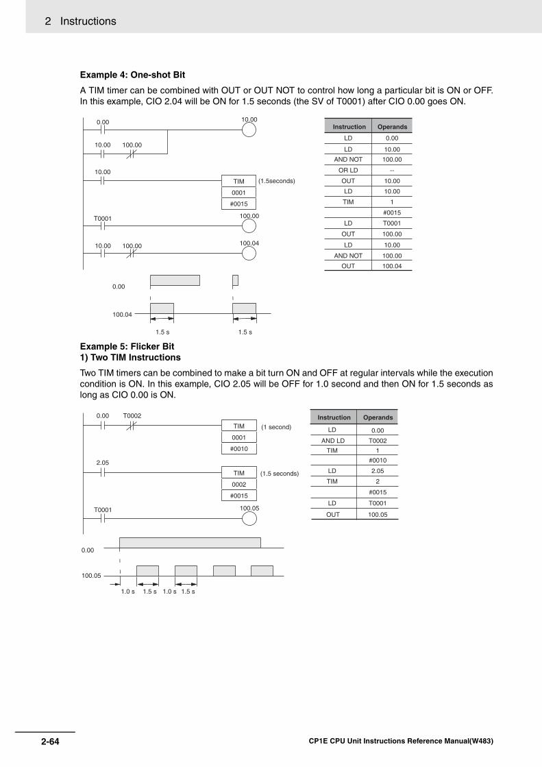
2 Instructions
Example 4: One-shot Bit
A TIM timer can be combined with OUT or OUT NOT to control how long a particular bit is ON or OFF.In this example, CIO 2.04 will be ON for 1.5 seconds (the SV of T0001) after CIO 0.00 goes ON.
Example 5: Flicker Bit1) Two TIM Instructions
Two TIM timers can be combined to make a bit turn ON and OFF at regular intervals while the executioncondition is ON. In this example, CIO 2.05 will be OFF for 1.0 second and then ON for 1.5 seconds aslong as CIO 0.00 is ON.
0.00
100.04
1.5 s 1.5 s
TIM
0001
#0015
10.00
10.00
0.00 10.00
T0001 100.00
10.00 100.04
100.00
100.00
(1.5seconds)
1
#0015
T0001
100.00
10.00
100.00
100.04
Operands
--OR LD
AND NOT
Instruction
0.00LD
TIM
LD
10.00LD
10.00OUT
10.00LD
OUT
OUT
LD
100.00AND NOT
TIM
0002
#0015
TIM
0001
#0010
100.05
2.05
0.00
T0001
T0002
0.00
100.05
1.5 s1.0 s 1.5 s1.0 s
(1 second)
(1.5 seconds)
LD
LD
LD
TIM
TIM
OUT
AND LD
Instruction
T0002
1
#0010
2.05
2
#0015
100.05
T0001
0.00
Operands
2-64 CP1E CPU Unit Instructions Reference Manual(W483)

2 Instructions T
imer an
d C
ou
nter In
structio
ns
2
2) Clock Pulse
The desired execution condition can be combined with a clock pulse to mimic the clock pulse (0.1 s, 0.2s, or 1.0 s).
Timer reset methodThere are two methods for resetting a timer instruction.
1. Turn OFF the execution condition for the timer instruction.
The timer will be reset when its execution condition turns OFF.
The timer will start timing again when its execution condition turns ON.
With this method, a timer cannot be reset and then restarted within the same cycle.
2. Use the RESET TIMER/COUNTER instruction.
The specified instruction will be reset when the RESET TIMER/COUNTER instruction (CNR/CNRX) isexecuted.
0.00
1s
A
A,B=0.5s
B
0.00 100.06
100.06
P. 1s (1-s clock pulse)
LD
OUT
AND
Instruction
1s
100.06
0.00
Operands
• The internal clock pulse (0.1 s, 0.2 s, 1 s) can beused to easily program a flicker circuit.
TIM
0010
#100
0.01
When CIO 0.01 turns ON, the timer starts timing.When CIO 0.01 turns OFF, the timer is reset.
ON
OFF
ON
OFF
Timer inputCIO 0.01
Timer PVT0010
Completion Flag
T0010
The timer cannot be reset and then restarted within the same cycle.
2-65CP1E CPU Unit Instructions Reference Manual(W483)
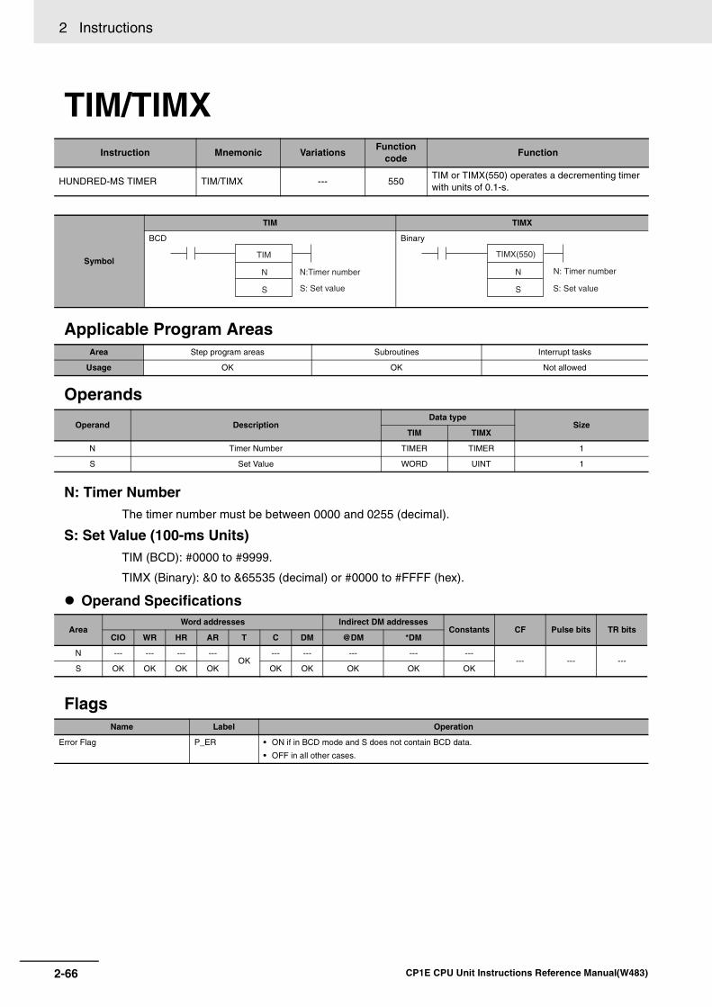
2 Instructions
TIM/TIMX
Applicable Program Areas
Operands
N: Timer NumberThe timer number must be between 0000 and 0255 (decimal).
S: Set Value (100-ms Units)TIM (BCD): #0000 to #9999.
TIMX (Binary): &0 to &65535 (decimal) or #0000 to #FFFF (hex).
Operand Specifications
Flags
Instruction Mnemonic VariationsFunction
codeFunction
HUNDRED-MS TIMER TIM/TIMX --- 550TIM or TIMX(550) operates a decrementing timer with units of 0.1-s.
Symbol
TIM TIMX
BCD Binary
Area Step program areas Subroutines Interrupt tasks
Usage OK OK Not allowed
Operand Description Data type
Size TIM TIMX
N Timer Number TIMER TIMER 1
S Set Value WORD UINT 1
Area Word addresses Indirect DM addresses
Constants CF Pulse bits TR bitsCIO WR HR AR T C DM @DM *DM
N --- --- --- ---OK
--- --- --- --- ------ --- ---
S OK OK OK OK OK OK OK OK OK
Name Label Operation
Error Flag P_ER • ON if in BCD mode and S does not contain BCD data.
• OFF in all other cases.
TIM
N
S S: Set value
N:Timer number
TIMX(550)
N
S S: Set value
N: Timer number
2-66 CP1E CPU Unit Instructions Reference Manual(W483)
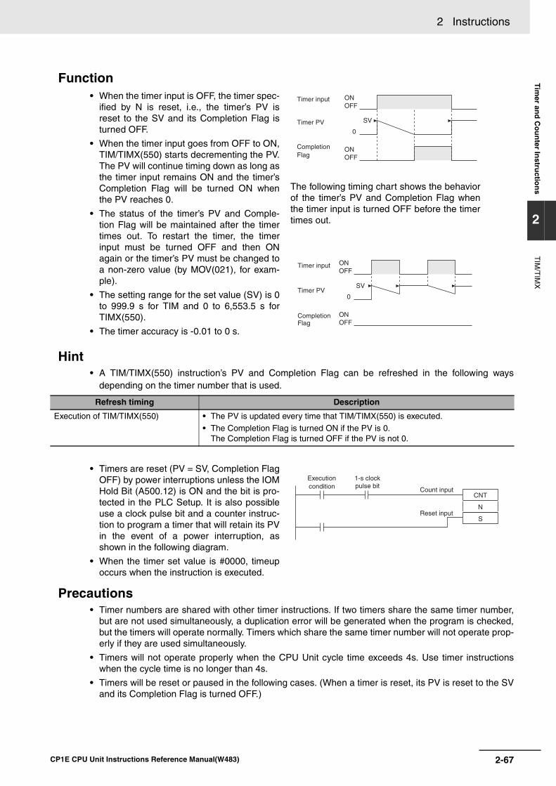
2 Instructions T
imer an
d C
ou
nter In
structio
ns
2
TIM
/TIM
X
Function
Hint• A TIM/TIMX(550) instruction’s PV and Completion Flag can be refreshed in the following ways
depending on the timer number that is used.
Precautions• Timer numbers are shared with other timer instructions. If two timers share the same timer number,
but are not used simultaneously, a duplication error will be generated when the program is checked,but the timers will operate normally. Timers which share the same timer number will not operate prop-erly if they are used simultaneously.
• Timers will not operate properly when the CPU Unit cycle time exceeds 4s. Use timer instructionswhen the cycle time is no longer than 4s.
• Timers will be reset or paused in the following cases. (When a timer is reset, its PV is reset to the SVand its Completion Flag is turned OFF.)
• When the timer input is OFF, the timer spec-ified by N is reset, i.e., the timer’s PV isreset to the SV and its Completion Flag isturned OFF.
• When the timer input goes from OFF to ON,TIM/TIMX(550) starts decrementing the PV.The PV will continue timing down as long asthe timer input remains ON and the timer’sCompletion Flag will be turned ON whenthe PV reaches 0.
• The status of the timer’s PV and Comple-tion Flag will be maintained after the timertimes out. To restart the timer, the timerinput must be turned OFF and then ONagain or the timer’s PV must be changed toa non-zero value (by MOV(021), for exam-ple).
• The setting range for the set value (SV) is 0to 999.9 s for TIM and 0 to 6,553.5 s forTIMX(550).
• The timer accuracy is -0.01 to 0 s.
Refresh timing Description
Execution of TIM/TIMX(550) • The PV is updated every time that TIM/TIMX(550) is executed.• The Completion Flag is turned ON if the PV is 0.
The Completion Flag is turned OFF if the PV is not 0.
• Timers are reset (PV = SV, Completion FlagOFF) by power interruptions unless the IOMHold Bit (A500.12) is ON and the bit is pro-tected in the PLC Setup. It is also possibleuse a clock pulse bit and a counter instruc-tion to program a timer that will retain its PVin the event of a power interruption, asshown in the following diagram.
• When the timer set value is #0000, timeupoccurs when the instruction is executed.
ONOFF
0
ONOFF
SV
Timer input
Timer PV
Completion Flag
ONOFF
0
ONOFF
SV
Timer input
Timer PV
CompletionFlag
The following timing chart shows the behaviorof the timer’s PV and Completion Flag whenthe timer input is turned OFF before the timertimes out.
CNT
N
S
Count input
Reset input
Execution condition
1-s clock pulse bit
2-67CP1E CPU Unit Instructions Reference Manual(W483)

2 Instructions
*1 If the IOM Hold Bit (A500.12) has been turned ON, the status of timer Completion Flags and PVs will be maintained whenthe operating mode is changed.
*2 The PV will be set to the SV when TIM/TIMX(550) is executed.
• When TIM/TIMX(550) is in a program section between IL(002) and ILC(003) and the program sectionis interlocked, the PV will be reset to the SV and the Completion Flag will be turned OFF.
• When an operating TIM/TIMX(550) timer is in a jumped program section (JMP(004), CJP(510),JME(005)), the timer’s PV will not be refreshed.
• When a TIM/TIMX(550) timer is forced set, its Completion Flag will be turned ON and its PV will beset to 0000. When a TIM/TIMX(550) timer is forced reset, its Completion Flag will be turned OFF andits PV will be reset to the SV.
• The timer’s Completion Flag is refreshed only when TIM/TIMX(550) is executed, so a delay of up toone cycle may be required for the Completion Flag to be turned ON after the timer times out.
• If online editing is used to overwrite a timer instruction, always reset the Completion Flag. The timerwill not operate properly unless the Completion Flag is reset.
Sample programWhen timer input CIO 0.00 goes from OFF to ON in the following example, the timer PV will begincounting down from the SV. Timer Completion Flag T0000 will be turned ON when the PV reaches 0.
When CIO 0.00 goes OFF, the timer PV will be reset to the SV and the Completion Flag will be turnedOFF.
i
Condition PV Completion Flag
Operating mode changed from RUN or MONITOR mode to PROGRAM mode or vice versa.*1
0 OFF
Power off and reset 0 OFF
Execution of CNR(545)/CNRX(547), the RESET TIMER/COUNTER instructions*2
BCD: 9999Binary: FFFF
OFF
Operation in interlocked program section (IL(002)–ILC(003))
Reset to SV. OFF
Operation in jumped program section(JMP(004)–JME(005))
Retains previous status.
Retains previous status.
0.00
100
T0000
T0000
or
0.00
TIM
0000
#0100
TIMX
0000
&0100
0.00
ONOFF
ONOFF
ONOFF
Timer input
Timer PV
Timer Completion Flag
2-68 CP1E CPU Unit Instructions Reference Manual(W483)
2 Instructions T
imer an
d C
ou
nter In
structio
ns
2
TIM
H/T
IMH
X
TIMH/TIMHX
Applicable Program Areas
Operands
N: Timer NumberThe timer number must be between 0000 and 0255 (decimal).
S: Set ValueTIMH (BCD): #0000 to #9999
TIMHX (Binary): &0 to &65535 (decimal) or #0000 to #FFFF (hex)
Operand Specifications
Flags
Instruction Mnemonic VariationsFunction
codeFunction
TEN-MS TIMERTIMH --- 015 TIMH(015)/TIMHX(551) operates a decrementing
timer with units of 10-ms.TIMHX --- 551
Symbol
TIMH TIMHX
BCD Binary
Area Step program areas Subroutines Interrupt tasks
Usage OK OK Not allowed
Operand Description Data type
Size TIMH TIMHX
N Timer Number TIMER TIMER 1
S Set Value WORD UINT 1
Area Word addresses Indirect DM addresses
Constants CF Pulse bits TR bitsCIO WR HR AR T C DM @DM *DM
N --- --- --- ---OK
--- --- --- --- ------ --- ---
S OK OK OK OK OK OK OK OK OK
Name Label Operation
Error Flag ER • ON if in BCD mode and S does not contain BCD data.
• OFF in all other cases.
TIMH(015)
N
S S: Set value
N: Timer number
TIMHX(551)
N
S S: Set value
N: Timer number
2-69CP1E CPU Unit Instructions Reference Manual(W483)
2 Instructions
Function
HintA TIMH(015)/TIMHX(551) instruction’s PV and Completion Flag can be refreshed in the following waysdepending on the timer number that is used.
Precautions• Timer numbers are shared with other timer instructions. If two timers share the same timer number,
but are not used simultaneously, a duplication error will be generated when the program is checked,but the timers will operate normally. Timers which share the same timer number will not operate prop-erly if they are used simultaneously.
• Timers will not operate properly when the CPU Unit cycle time exceeds 4s. Use timer instructionswhen the cycle time is no longer than 4s.
• Timers will be reset or paused in the following cases. (When a timer is reset, its PV is reset to the SVand its Completion Flag is turned OFF.)
• When the timer input is OFF, the timer specifiedby N is reset, i.e., the timer’s PV is reset to theSV and its Completion Flag is turned OFF.
• When the timer input goes from OFF to ON,TIMH(015)/TIMHX(551) starts decrementing thePV. The PV will continue timing down as long asthe timer input remains ON and the timer’s Com-pletion Flag will be turned ON when the PVreaches 0000.
• The status of the timer’s PV and Completion Flagwill be maintained after the timer times out. Torestart the timer, the timer input must be turnedOFF and then ON again or the timer’s PV mustbe changed to a non-zero value (by MOV(021),for example).
• The setting range for the set value (SV) is 0 to99.99 s for TIMH(015) and 0 to 655.35 s forTIMHX(551).
• The timer accuracy is 0 to 0.01 s.
Refresh timing Description
Execution of TIMH(015)/TIMHX(551) • The PV is updated every time that TIMH(015)/TIMHX(551) is executed.• The Completion Flag is turned ON if the PV is 0.
The Completion Flag is turned OFF if the PV is not 0.
ONOFF
0
ONOFF
SV
Timer input
Timer PV
Completion Flag
ONOFF
0
ONOFF
SV
Timer input
Timer PV
Completion Flag
The following timing chart shows thebehavior of the timer’s PV and CompletionFlag when the timer input is turned OFFbefore the timer times out.
2-70 CP1E CPU Unit Instructions Reference Manual(W483)

2 Instructions T
imer an
d C
ou
nter In
structio
ns
2
TIM
H/T
IMH
X
*1 If the IOM Hold Bit (A500.12) has been turned ON, the status of timer Completion Flags and PVs will be maintained whenthe operating mode is changed.
*2 The PV will be set to the SV when TIMH(015)/TIMHX(551) is executed.
• When an operating TIMH(015)/TIMHX(551) timer is in a jumped program section (JMP(004),CJP(510), JME(005)), the timer’s PV will not be refreshed in the above case.
• When TIMH(015)/TIMHX(551) is in a program section between IL(002) and ILC(003) and the pro-gram section is interlocked, the PV will be reset to the SV and the Completion Flag will be turnedOFF.
• When a TIMH(015)/TIMHX(551) timer is forced set, its Completion Flag will be turned ON and its PVwill be set to 0000. When a TIMH(015)/TIMHX(551) timer is forced reset, its Completion Flag will beturned OFF and its PV will be reset to the SV.
• The timer’s Completion Flag is refreshed only when TIMH(015)/TIMHX(551) is executed, so a delayof up to one cycle may be required for the Completion Flag to be turned ON after the timer times out.
• If online editing is used to overwrite a timer instruction, always reset the Completion Flag. The timerwill not operate properly unless the Completion Flag is reset.
Sample programWhen timer input CIO 0.00 goes from OFF to ON in the following example, the timer PV will begincounting down from the SV (#0064 = 100 = 1.00 s). The Timer Completion Flag, T0000, will be turnedON when the PV reaches 0.
When CIO 0.00 goes OFF, the timer PV will be reset to the SV and the Completion Flag will be turnedOFF.
i
Condition PV Completion Flag
Operating mode changed from RUN or MONITOR mode to PROGRAM mode or vice versa.*1
0 OFF
Power off and reset 0 OFF
Execution of CNR(545)/CNRX(547), the RESET TIMER/COUNTER instructions*2
BCD: 9999Binary: FFFF
OFF
Operation in interlocked program section (IL(002)-ILC(003))
Reset to SV. OFF
Operation in jumped program section
(JMP(004)-JME(005))
Retains previous status.
Retains previous status.
0.000.00
0.00
T0000
T0000
100(1.00 s)
or
ONOFF
ON
0
&100
TIMHX
0
100
OFF
0
#0100
TIMH
Timer input
Timer PV
Timer Completion Flag
2-71CP1E CPU Unit Instructions Reference Manual(W483)

2 Instructions
TMHH/TMHHX
Applicable Program Areas
Operands
N: Timer NumberThe timer must be between 0000 and 0015 decimal.
S: Set ValueTMHH (BCD): #0000 to #9999
TMHHX (Binary): &0 to &65535 (decimal) or #0000 to #FFFF (hex)
Operand Specifications
Flags
Function• When the timer input is OFF, the timer specified by N is reset, i.e., the timer’s PV is reset to the SV
and its Completion Flag is turned OFF.
• When the timer input goes from OFF to ON, TMHH(540)/TMHHX(552) starts decrementing the PV.The PV will continue timing down as long as the timer input remains ON and the timer’s CompletionFlag will be turned ON when the PV reaches 0000.
• The status of the timer’s PV and Completion Flag will be maintained after the timer times out. Torestart the timer, the timer input must be turned OFF and then ON again or the timer’s PV must bechanged to a non-zero value (by MOV(021), for example).
Instruction Mnemonic VariationsFunction
codeFunction
ONE-MS TIMERTMHH --- 540 TMHH(540)/TMHHX(552) operates a decrement-
ing timer with units of 1-ms.TMHHX --- 552
Symbol
TMHH TMHHX
BCD Binary
Area Step program areas Subroutines Interrupt tasks
Usage OK OK Not allowed
Operand Description Data type
Size TMHH TMHHX
N Timer Number TIMER TIMER 1
S Set Value WORD UINT 1
Area Word addresses Indirect DM addresses
Constants CF Pulse bits TR bitsCIO WR HR AR T C DM @DM *DM
N --- --- --- ---OK
--- --- --- --- ------ --- ---
S OK OK OK OK OK OK OK OK OK
Name Label Operation
Error Flag P_ER • ON if in BCD mode and S does not contain BCD data.
• OFF in all other cases.
TMHH(540)
N
S S: Set value
N: Timer number
TMHHX(552)
N
S S: Set value
N: Timer number
2-72 CP1E CPU Unit Instructions Reference Manual(W483)

2 Instructions T
imer an
d C
ou
nter In
structio
ns
2
TM
HH
/TM
HH
X
• The setting range for the set value (SV) is 0 to 9.999 s for TMHH(540) and 0 to 65.535 forTMHHX(552).
• The timer accuracy is -0.001 to 0 s.
HintThe timer PV and timeup used in TMHH/TMHHX instructions are refreshed at the timing below.
Precautions• Timer numbers are shared with other timer instructions. If two timers share the same timer number,
but are not used simultaneously, a duplication error will be generated when the program is checked,but the timers will operate normally. Timers which share the same timer number will not operate prop-erly if they are used simultaneously.
• The Completion Flag is updated only when TMHH(540)/TMHHX(552) is executed. The CompletionFlag can thus be delayed by up to one cycle time from the actual set value.
• The present value of a timer will not be refreshed even if the task is on standby.
• Timers will be reset or paused in the following cases. (When a timer is reset, its PV is reset to the SVand its Completion Flag is turned OFF.)
*1 If the IOM Hold Bit (A500.12) has been turned ON, the status of timer Completion Flags and PVs will be maintained whenthe operating mode is changed.
*2 The PV will be set to the SV when TMHH(540)/TMHHX(552) is executed.
• The present value of all operating timers will not be refreshed even if the timer is in a program sectionthat is jumped using JMP(004), CJP(510), JME(005).
• When TMHH(540)/TMHHX(552) is in a program section between IL(002) and ILC(003) and the pro-gram section is interlocked, the PV will be reset to the SV and the Completion Flag will be turnedOFF.
• When a TMHH(540)/TMHHX(552) timer is forced set, its Completion Flag will be turned ON and itsPV will be set to 0. When a TMHH(540)/TMHHX(552) timer is forced reset, its Completion Flag will beturned OFF and its PV will be reset to the SV.
• If online editing is used to overwrite a timer instruction, always reset the Completion Flag. The timerwill not operate properly unless the Completion Flag is reset.
Refresh timing Description
When each instruction is executed • The PV is updated every time that each instruction is executed.• The timeup flag is ON when the PV is 0 and OFF otherwise.
Condition PV Completion Flag
Operating mode changed from RUN or MONITOR mode to PROGRAM mode or vice versa.*1
0 OFF
Power supply interrupted and reset 0 OFF
Execution of CNR(545)/CNRX(547), the RESET TIMER/COUNTER instructions*2
BCD: 9999Binary: FFFF
OFF
Operation in interlocked program section (IL(002)-ILC(003))
Reset to SV. OFF
Operation in jumped program section
(JMP(004)-JME(005))
Retains previous status.
Retains previous status.
2-73CP1E CPU Unit Instructions Reference Manual(W483)
2 Instructions
TTIM/TTIMX
Applicable Program Areas
Operands
N: Timer NumberThe timer number must be between 0000 to 0255 (decimal).
S: Set ValueTTIM (BCD): #0000 to #9999
TTIMX (Binary): &0 to &65535 (decimal) or #0000 to #FFFF (hex)
Operand Specifications
Flags
Instruction Mnemonic VariationsFunction
codeFunction
ACCUMULATIVE TIMERTTIM --- 087 TTIM(087)/TTIMX(555) operates an incrementing
timer with units of 0.1-s.TTIMX --- 555
Symbol
TTIM TTIMX
BCD Binary
Area Step program areas Subroutines Interrupt tasks
Usage OK OK Not allowed
Operand Description Data type
Size TTIM TTIMX
N Timer Number TIMER TIMER 1
S Set Value WORD UINT 1
Area Word addresses Indirect DM addresses
Constants CF Pulse bits TR bitsCIO WR HR AR T C DM @DM *DM
N --- --- --- ---OK
--- --- --- --- ------ --- ---
S OK OK OK OK OK OK OK OK OK
Name Label Operation
Error Flag P_ER • ON if in BCD mode and S does not contain BCD data.
• OFF in all other cases.
TTIM(087)
N
S
Timer input
Reset inputS: Set value
N: Timer number
TTIMX(555)
N
S
Timer input
Reset inputS: Set value
N: Timer number
2-74 CP1E CPU Unit Instructions Reference Manual(W483)
2 Instructions T
imer an
d C
ou
nter In
structio
ns
2
TT
IM/T
TIM
X
Function
Hint• Typical timers such as TIM/TIMX(550) are decrementing counters and the PV shows the time remain-
ing until the timer times out. The PV of TTIM(087)/TTIMX(555) shows how much time has elapsed,so the PV can be used unchanged in many calculations and display outputs.
Precautions• Timer numbers are shared with other timer instructions. If two timers share the same timer number,
but are not used simultaneously, a duplication error will be generated when the program is checked,but the timers will operate normally. Timers which share the same timer number will not operate prop-erly if they are used simultaneously.
• Timers will be reset or paused in the following cases. (When a TTIM(087)/TTIMX(555) timer is reset,its PV is reset to 0 and its Completion Flag is turned OFF.)
*1 If the IOM Hold Bit (A500.12) has been turned ON, the status of timer Completion Flags and PVs will be maintained whenthe operating mode is changed.
*2 The PV will be set to the SV when TTIM(087)/TTIMX(555) is executed.
• When TTIM(087)/TTIMX(555) is in a program section between IL(002) and ILC(003) and the programsection is interlocked, the PV will retain its previous value (it will not be reset). Be sure to take this factinto account when TTIM(087)/TTIMX(555) is programmed between IL(002) and ILC(003).
• When an operating TTIM(087)/TTIMX(555) timer is in a program section between JMP(004) andJME(005) and the program section is jumped, the PV will retain its previous value. Be sure to takethis fact into account when TTIM(087)/TTIMX(555) is programmed between JMP(004) andJME(005).
• When the timer input is ON,TTIM(087)/TTIMX(555) increments the PV.When the timer input goes OFF, the timerwill stop incrementing the PV, but the PV willretain its value. The PV will resume timingwhen the timer input goes ON again. Thetimer’s Completion Flag will be turned ONwhen the PV reaches the SV.
• The status of the timer’s PV and CompletionFlag will be maintained after the timer timesout. There are three ways to restart thetimer: the timer’s PV can be changed to anon-zero value (by MOV(021), for example),the reset input can be turned ON, orCNR(545)/CNRX(547) can be executed.
• The setting range for the set value (SV) is 0to 999.9 s for TTIM(087) and 0 to 6,553.5 sfor TTIMX(555).
• The timer accuracy is 0 to 0.01 s.
Condition PV Completion Flag
Operating mode changed from RUN or MONITOR mode to PROGRAM mode or vice versa.*1
0 OFF
Power supply interrupted and reset 0 OFF
Execution of CNR(545)/CNRX(547), the RESET TIMER/COUNTER instructions*2
BCD: 9999Binary: FFFF
OFF
Operation in interlocked program section (IL(002)-ILC(003))
Retains previous status.
Retains previous status.
Operation in jumped program section
(JMP(004)-JME(005))
Retains previous status.
Retains previous status.
ONOFF
0
ONOFF
ONOFF
Timer input
Timer PV
Reset input
Completion Flag
SV
PV maintained.
Timing resumes.
2-75CP1E CPU Unit Instructions Reference Manual(W483)

2 Instructions
• When a TTIM(087)/TTIMX(555) timer is forced set, its Completion Flag will be turned ON and its PVwill be reset to 0. When a TTIM(087)/TTIMX(555) timer is forced reset, its Completion Flag will beturned OFF and its PV will be reset to 0. The forced set and forced reset operations take priority overthe status of the timer and reset inputs.
• The timer’s PV is refreshed only when TTIM(087)/TTIMX(555) is executed, so the timer will not oper-ate properly when the cycle time exceeds 100 ms because the timer increments in 100-ms units.
• The timer’s Completion Flag is refreshed only when TTIM(087)/TTIMX(555) is executed, so a delay ofup to one cycle may be required for the Completion Flag to be turned ON after the timer times out.
Sample programWhen timer input CIO 0.00 is ON in the following example, the timer PV will begin counting up from 0.Timer Completion Flag T0001 will be turned ON when the PV reaches the SV.
If the reset input is turned ON, the timer PV will be reset to 0 and the Completion Flag (T0001) will beturned OFF. (Usually the reset input is turned ON to reset the timer and then the timer input is turnedON to start timing.)
If the timer input is turned OFF before the SV is reached, the timer will stop timing but the PV will bemaintained. The timer will resume from its previous PV when the timer input is turned ON again.
0.00
T0001
T0001
Timer input
Timer PV
Timer Completion Flag
Reset input
PV maintained.
Timing resumes.
or
ONOFF
0
ONOFF
ONOFF
#0100
ONOFF
0
ONOFF
ONOFF
#0100
0.01
TTIM
0001
#0100
0.00
TTIMX
0001
&0100
0.00
0.01
2-76 CP1E CPU Unit Instructions Reference Manual(W483)

2 Instructions T
imer an
d C
ou
nter In
structio
ns
2
TIM
L/TIM
LX
TIML/TIMLX
Applicable Program Areas
Operands
Operand Specifications
Flags
Instruction Mnemonic VariationsFunction
codeFunction
LONG TIMERTIML --- 542 TIML(542)/TIMLX(553) operates a decrementing
timer with units of 0.1s.TIMLX --- 553
Symbol
TIML TIMLX
BCD Binary
Area Step program areas Subroutines Interrupt tasks
Usage OK OK Not allowed
Operand Description Data type
Size TIML TIMLX
D1 Completion Flag WORD UINT 1
D2 PV word DWORD UDINT 2
S SV word DWORD UDINT 2
D1: Completion Flag
D2: PV Word
S: SV Word
The PV and SV can range from #00000000to #99999999 for TIML(542) and &00000000to &4294967294 (decimal) or #00000000 to#FFFFFFFF (hexadecimal) for TIMLX(553).
Note S, S+1, D2 and D2+1 must be in the samedata area.
Area Word addresses Indirect DM addresses
Constants CF Pulse bits TR bitsCIO WR HR AR T C DM @DM *DM
D1,D2OK OK OK OK
--- ---OK OK OK
------ --- ---
S OK OK OK
Name Label Operation
Error Flag P_ER • ON if in BCD mode and D2 does not contained BCD data.
• ON if in BCD mode and S does not contained BCD data.
• OFF in all other cases.
TIML(542)
D1
D2
S
D1: Completion Flag
D2: PV word
S: SV word
TIMLX(553)
D1
D2
S
D1: Completion Flag
D2: PV word
S: SV word
15D1
0
Completion FlagDo not use.
D2D2+1D2D2+1 is the leftmost 4 digits, D2 is the rightmost 4 digits
SS+1SS+1 is the leftmost 4 digits, S is the rightmost 4 digits
2-77CP1E CPU Unit Instructions Reference Manual(W483)
2 Instructions
Function
• TIML(542)/TIMLX(553) can time up to 115 days for TIML(542) and 4,971 days for TIMLX(553).
• The timer accuracy is 0 to 0.01 s.
Precautions• Unlike most timers, TIML(542)/TIMLX(553) does not use a timer number. (Timer area PV refreshing
is not performed for TIML(542)/TIMLX(553).)
• Since the Completion Flag for TIML(542)/TIMLX(553) is in a data area it can be forced set or forcedreset like other bits, but the PV will not change.
• The timer’s PV is refreshed only when TIML(542)/TIMLX(553) is executed, so the timer will not oper-ate properly when the cycle time exceeds 100 ms because the timer increments in 100-ms units.
• The timer’s Completion Flag is refreshed only when TIML(542)/TIMLX(553) is executed, so a delay ofup to one cycle may be required for the Completion Flag to be turned ON after the timer times out.
• When TIML(542)/TIMLX(553) is in a program section between IL(002) and ILC(003) and the programsection is interlocked, the PV will be reset to the SV and the Completion Flag will be turned OFF.
• When an operating TIML(542)/TIMLX(553) timer is in a program section between JMP(004) andJME(005) and the program section is jumped, the PV will retain its previous value. Be sure to takethis fact into account when TIML(542)/TIMLX(553) is programmed between JMP(004) and JME(005).
• Be sure that the words specified for the Completion Flag and PV (D1, D2, and D2+1) are not used inother instructions. If these words are affected by other instructions, the timer might not time out properly.
• When the timer input is OFF, the timer isreset, i.e., the timer’s PV is reset to the SVand its Completion Flag is turned OFF.
• When the timer input goes from OFF to ON,TIML(542)/TIMLX(553) starts decrementingthe PV in D2+1 and D2. The PV will con-tinue timing down as long as the timer inputremains ON and the timer’s CompletionFlag will be turned ON when the PVreaches 0.
• The status of the timer’s PV and Comple-tion Flag will be maintained after the timertimes out. To restart the timer, the timerinput must be turned OFF and then ONagain or the timer’s PV must be changed toa non-zero value (by MOV(021), for exam-ple).
ONOFF
0
ONOFF
SV
Timer input
Timer PV
Completion Flag (Bit 00 of D1)
2-78 CP1E CPU Unit Instructions Reference Manual(W483)
2 Instructions T
imer an
d C
ou
nter In
structio
ns
2
TIM
L/TIM
LX
Sample programWhen timer input CIO 0.00 is ON in the following example, the timer PV (in D201 and D200) will be setto the SV (in D101 and D100) and the PV will begin counting down. The timer Completion Flag (CIO200.00) will be turned ON when the PV reaches 0.
When CIO 0.00 goes OFF, the timer PV will be reset to the SV and the Completion Flag will be turnedOFF.
TIML
200
D100
D200
0.00 ONOFF
0
ONOFF
D1
D2
S
D1:200
0123456789101112131415
D2:D100
D101
015
D200D201
#0010 #0000
(CIO 0200.00)
Timer SVS: D200 and upS+1: Content of D2011000.00
Timer input
Timer PV(D101 and D100)
Timer CompletionFlag(CIO 200.00)
Timer SV:(100,000 decimal= 10,000 s)
Timer’s PV (LSB)
Timer’s PV (MSB)
Timer Completion Flag
2-79CP1E CPU Unit Instructions Reference Manual(W483)

2 Instructions
CNT/CNTX
Applicable Program Areas
Operands
N: Counter NumberThe counter number must be between 0000 and 0255 (decimal).
S: Set Value CNT (BCD): #0000 to #9999 CNTX (Binary): &0 to &65535 (decimal) or #0000 to #FFFF (hex)
Operand Specifications
Flags
Instruction Mnemonic VariationsFunction
codeFunction
COUNTER CNT/CNTX --- 546CNT/CNTX(546) operates a decrementing counter.
Symbol
CNT CNTX
BCD Binary
Area Step program areas Subroutines Interrupt tasks
Usage OK OK OK
Operand Description Data type
Size CNT CNTX
N Counter Number COUNTER COUNTER 1
S Set Value WORD UINT 1
Area Word addresses Indirect DM addresses
Constants CF Pulse bits TR bitsCIO WR HR AR T C DM @DM *DM
N --- --- --- --- ---OK
--- --- --- --- --- ------
S OK OK OK OK OK OK OK OK OK OK OK
Name Label Operation
Error Flag P_ER • ON if in BCD mode and S does not contain BCD data.
• OFF in all other cases.
CNT
N
S
Count input
Reset inputN: Counter number
S: Set value
CNTX(546)
N
S
Count input
Reset inputN: Counter number
S: Set value
2-80 CP1E CPU Unit Instructions Reference Manual(W483)
2 Instructions T
imer an
d C
ou
nter In
structio
ns
2
CN
T/C
NT
X
Function
• The setting range 0 to 9,999 for CNT and 0 to 65,535 for CNTX(546).
Hint
Precautions• Counter numbers are shared by the CNT, CNTX(546), CNTR(012) and CNTRX(548) instructions. If
two counters share the same counter number but are not used simultaneously, a duplication error willbe generated when the program is checked but the counters will operate normally. Counters whichshare the same counter number will not operate properly if they are used simultaneously.
• A counter’s PV is refreshed when the count input goes from OFF to ON and the Completion Flag isrefreshed each time that CNT/CNTX(546) is executed. The Completion Flag is turned ON if the PV is0 and it is turned OFF if the PV is not 0.
• The counter PV is decremented by 1 everytime that the count input goes from OFF toON. The Completion Flag is turned ONwhen the PV reaches 0.
• Once the Completion Flag is turned ON,reset the counter by turning the reset inputON or by using the CNR(545)/CNRX(547)instruction. Otherwise, the counter cannotbe restarted.
• The counter is reset and the count input isignored when the reset input is ON. (Whena counter is reset, its PV is reset to the SVand the Completion Flag is turned OFF.)
• Counter PVs are retained even through apower interruption. If you want to restartcounting from the SV instead of resumingthe count from the retained PV, add theFirst Cycle Flag (A200.11) as a reset inputto the counter.
Note 1 In case CP1E CPU Unit is backed up in the capacitor and power remained OFF for a period in excess ofthe following, the Counters PVs and Countup Flags are unfixed.E-type CPU Unit9 hours (60°C), 50 hours (25°C)N/NA-type CPU Unit7 hours (60°C), 40 hours (25°C)
2 By setting “Zero Clear Holding Memory” for the PLC Setup, the Counters PVs and Countup Flags will becleared each time power turns ON. In this case, the DM area (D) and Holding Area (H) will be cleared atthe same time.
3 N/NA-type CP1E CPU Unit (CP1E-N/NAD-) can be equipped with a battery. With the batteryinstalled, the Counters PVs and Countup Flags can be retained during power OFF.
ON
OFF
ON
OFF
ON
OFF
0
SV
Count input
Counter PV
Reset input
Completion Flag
CNT
N
S
First Cycle Flag (A200.11)
2-81CP1E CPU Unit Instructions Reference Manual(W483)
2 Instructions
• When a CNT/CNTX(546) counter is forced set, its Completion Flag will be turned ON and its PV willbe reset to 0000. When a CNT/CNTX(546) counter is forced reset, its Completion Flag will be turnedOFF and its PV will be set to the SV.
• If online editing is used to add a counter, the counter must be reset before it will work properly. If thecounter is not reset, the previous value will be used as the counter’s present value (PV), and thecounter may not operate properly after it is written.
• Be sure to reset the counter by turning the reset input from OFF → ON → OFF before beginningcounting with the count input, as shown in the following diagram. The count input will not be receivedif the reset input is ON.
• The reset input will take precedence and the counter will be reset if the reset input and count inputare both ON at the same time. (The PV will be reset to the SV and the Completion Flag will be turnedOFF.)
ON
OFF
ON
OFF
0
ON
OFF
Reset input
Counter PV
Count input
Ready to start counting
Completion Flag
SV
ON
OFF
ON
OFF
0
ON
OFF
ON
OFF
ON
OFF
SV
Reset input
Counter PV
Count input
Completion Flag
Count input can be received.
Reset input takes precedence.
Count input can be received.
2-82 CP1E CPU Unit Instructions Reference Manual(W483)

2 Instructions T
imer an
d C
ou
nter In
structio
ns
2
CN
TR
/CN
TR
X
CNTR/CNTRX
Applicable Program Areas
Operands
N: Counter NumberThe counter number must be between 0000 and 0255(decimal).
S: Set ValueCNTR (BCD):#0000 to #9999 CNTRX (Binary): &0 to &65535 (decimal) or #0000 to #FFFF (hex)
Operand Specifications
Flags
Instruction Mnemonic VariationsFunction
codeFunction
REVERSIBLE COUNTERCNTR --- 012
---CNTRX --- 548
Symbol
CNTR CNTRX
BCD Binary
Area Step program areas Subroutines Interrupt tasks
Usage OK OK OK
Operand Description Data type
Size CNTR CNTRX
N Counter Number COUNTER COUNTER 1
S Set Value WORD UINT 1
Area Word addresses Indirect DM addresses
Constants CF Pulse bits TR bitsCIO WR HR AR T C DM @DM *DM
N --- --- --- --- ---OK
--- --- --- ------ --- ---
S OK OK OK OK OK OK OK OK OK
Name Label Operation
Error Flag P_ER • ON if in BCD mode and S does not contain BCD data.
• OFF in all other cases.
Increment input
Reset input
Decrement inputN: Counter number
S: Set value
CNTR(012)
N
S
Increment input
Reset input
Decrement inputN: Counter number
S: Set value
CNTRX(548)
N
S
2-83CP1E CPU Unit Instructions Reference Manual(W483)

2 Instructions
Function
Precautions• Counter numbers are shared by the CNT, CNTX(546), CNTR(012) and CNTRX(548) instructions. If
two counters share the same counter number but are not used simultaneously, a duplication error willbe generated when the program is checked but the counters will operate normally. Counters whichshare the same counter number will not operate properly if they are used simultaneously.
• The PV will not be changed if the increment and decrement inputs both go from OFF to ON at thesame time. When the reset input is ON, the PV will be reset to 0 and both count inputs will beignored.
• The Completion Flag will be ON only when the PV has been incremented from the SV to 0 or decre-mented from 0 to the SV; it will be OFF in all other cases.
• When inputting the CNTR(012)/CNTRX(548) instruction with mnemonics, first enter the incrementinput (II), then the decrement input (DI), the reset input (R), and finally the CNTR(012)/CNTRX(548)instruction. When entering with the ladder diagrams, first input the increment input (II), then theCNTR(012)/CNTRX(548) instruction, the decrement input (DI), and finally the reset input (R).
Sample programThe counter PV is reset to 0 by turning the reset input (CIO 0.02) ON and OFF. The PV is incrementedby 1 each time that the increment input (CIO 0.00) goes from OFF to ON. When the PV is incrementedfrom the SV (3), it is automatically reset to 0 and the Completion Flag is turned ON.
Likewise, the PV is decremented by 1 each time that the decrement input (CIO 0.01) goes from OFF toON. When the PV is decremented from 0, it is automatically set to the SV (3) and the Completion Flagis turned ON.
The counter PV is incremented by 1 everytime that the increment input goes from OFFto ON and it is decremented by 1 every timethat the decrement input goes from OFF toON. The PV can fluctuate between 0 and theSV.
When incrementing, the Completion Flag willbe turned ON when the PV is incrementedfrom the SV back to 0 and it will be turnedOFF again when the PV is incremented from0 to 1.
When decrementing, the Completion Flag willbe turned ON when the PV is decrementedfrom 0 up to the SV and it will be turned OFFagain when the PV is decremented from theSV to SV-1.
0
0
ON
OFF
0
ON
OFF
Increment input
Counter PV
Decrement input
SV
+1
Counter PV
Completion Flag
SV -1Counter PV
Completion Flag
2-84 CP1E CPU Unit Instructions Reference Manual(W483)
2 Instructions T
imer an
d C
ou
nter In
structio
ns
2
CN
TR
/CN
TR
X
The add and subtract count inputs increase/decrease the count once when the signal rises (OFF toON). When both inputs turn ON at the same time, neither increases/decreases the count. When thereset input turns ON, the PV changes to 0 and count input is not accepted.
In the following example, the SV for CNTR(012) 0007 is determined by the content of CIO 0001. Whenthe content of CIO 0001 is controlled by an external switch, the set value can be changed manuallyfrom the switch.
SV
Increment input0.00
Counter PVC0001
Completion FlagC0001
Decrement input0.01
Reset input0.02
Increment input
Reset input
Decrement input
CNTR
0001
#0003
0.00
0.01
0.02
CNTRX
0001
&3
0.00
0.01
0.02
or
ON
OFF
ON
OFF
ON
OFF
ON
OFF
3
0
Increment input
Reset input
Decrement input
CNTR
0006
#5000
CNTR
0007
1
0.00
0.01
0.02
C0006
0.03
0.04
0.05
C0007
200.07
200.08
4999 5000 0 1 2
4999500001
SV:CIO 0001
Increment input
Decrement input
Completion FlagRoll-over Roll-over
Fixed SV: 5000
0.00
0.01
0.02
#5000
200.07
0.03
0.04
0.05
0007
1
C0007
200.08
CNTR (012)
CNTR (012)
LD NOT
0006
Instruction Operands
LD
OUT
LD
LD
LD
LD
OUT
LD
LD
2-85CP1E CPU Unit Instructions Reference Manual(W483)

2 Instructions
CNR/CNRX
Applicable Program Areas
Operands
N1: First Number in RangeN1 must be a timer number between T000 and T255 or a counter number between C000 and C255.
N2: Last Number in RangeN2 must be a timer number between T000 and T255 or a counter number between C000 and C255.
Operand Specifications
Flags
FunctionCNR(545)/CNRX(547) resets the Completion Flags of all timers or counters from N1 to N2. At the sametime, the PVs will all be set to the maximum value (9999 for BCD and FFFF for binary). (The PV will beset to the SV the next time that the timer or counter instruction is executed.)
Instruction Mnemonic VariationsFunction
codeFunction
RESET TIMER/COUNTERCNR @CNR 545 Resets the timers or counters within the specified
range of timer or counter numbers.CNRX @CNRX 547
Symbol
CNR CNRX
BCD Binary
Area Step program areas Subroutines Interrupt tasks
Usage OK OK OK
Operand Description Data type
Size CNT CNTX
N1 First number in range TIMER/COUNTER*1 Variable
N2 Last number in range TIMER/COUNTER*1 Variable
Area Word addresses Indirect DM addresses
Constants CF Pulse bits TR bitsCIO WR HR AR T C DM @DM *DM
N1,N2 --- --- --- --- OK OK --- --- --- --- --- --- ---
Name Label Operation
Error Flag P_ER • ON if N1 and N2 are not in the same data area.
• OFF in all other cases.
CNR(545)
N1
N2
N1: First number in range
N2: Last number in range
CNRX(547)
N1
N2
N1: First number in range
N2: Last number in range
2-86 CP1E CPU Unit Instructions Reference Manual(W483)
2 Instructions T
imer an
d C
ou
nter In
structio
ns
2
CN
R/C
NR
X
Precautions• The timer/counter that is reset is as follows.
• The CNR(545)/CNRX(547) instructions do not reset TIML(542) and TIMLX(553), because these tim-ers do not use timer numbers.
• The CNR(545)/CNRX(547) instructions do not reset the timer/counter instructions themselves, theyreset the PVs and Completion Flags allocated to those instructions. In most cases, the effect ofCNR(545)/CNRX(547) is different from directly resetting the instructions. For example, when aTIM/TIMX(550) instruction is reset directly its PV is set to the SV, but when that timer is reset byCNR(545)/CNRX(547) its PV is set to the maximum value (9999 for BCD and FFFF for binary).
• When N1 and N2 are specified with N1>N2, only the Completion Flag for the timer/counter numberwill be reset.
Sample program
T
Instructions reset Operation of CNR(545)
BCD TIM: HUNDRED-MS TIMERTIMH(015): TEN-MS TIMERTMHH(540): ONE-MS TIMERTTIM(087): ACCUMULATIVE TIMERCNT: COUNTERCNTR(012): REVERSIBLE COUNTER
The PV is set to its maximum value (9,999 BCD) and the Completion Flag is turned OFF.
Instructions reset Operation of CNRX(547)
Binary TIMX(550): HUNDRED-MS TIMERTIMHX(551): TEN-MS TIMERTMHHX(552): ONE-MS TIMERTTIMX(555): ACCUMULATIVE TIMERCNTX(546): COUNTERCNTRX(548): REVERSIBLE COUNTER
The PV is set to its maximum value (FFFF hex) and the Completion Flag is turned OFF.
CNR
T0002
T0005
0.00
CNR
C0003
C0007
0.01
CNRX
T0002
T0005
0.00
CNRX
C0003
C0007
0.01
When CIO 0.00 is ON in the following example, the Completion Flags for timers T0002 to T0005 are turned OFF and the timers’ PVs are set to the maximum value (9999 for BCD).
When CIO 0.01 is ON, the Completion Flags for counters C0003 to C0007 are turned OFF and the counters’ PVs are set to the maximum value (9999 for BCD).
When CIO 0.00 is ON in the following example, the Completion Flags for timers T0002 to T0005 are turned OFF and the timers’ PVs are set to the maximum value (FFFF for binary).
When CIO 0.01 is ON, the Completion Flags for counters C0003 to C0007 are turned OFF and the counters’ PVs are set to the maximum value (FFFF for binary).
2-87CP1E CPU Unit Instructions Reference Manual(W483)
2 Instructions
Comparison Instructions
=, <>, <, <=, >, >=
Applicable Program Areas
Operands
Operand Specifications
Flags
Instruction Mnemonic VariationsFunction
codeFunction
Input Comparison Instructions=, <>, <, <=, >, >=
--- 300 to 328
Input comparison instructions compare two values (constants and/or the contents of specified words) and create an ON execution condition when the comparison condition is true. Input comparison instructions are available to compare signed or unsigned data of one-word or double length data.
Symbol
=, <>, <, <=, >, >=
LD connection AND connection OR connection
Area Step program areas Subroutines Interrupt tasks
Usage OK OK OK
Operand Description
Data type Size
UnsignedUnsigned
double lengthSigned
Signed double length
One-word Double length
S1 Comparison data 1 UINT UDINT INT DINT 1 2
S2 Comparison data 2 UINT UDINT INT DINT 1 2
Area Word addresses Indirect DM addresses
Constants CF Pulse bitsTR
bitsCIO WR HR AR T C DM @DM *DM
S1,S2 OK OK OK OK OK OK OK OK OK OK --- --- ---
Name Label Operation
Data length: one-word Data length: double length
Error Flag P_ER OFF or unchanged OFF or unchanged
Greater Than Flag P_GT • ON if S1 > S2 with one-word data.
• OFF in all other cases.
• ON if S1+1, S1 > S2+1, S2 with double-length data.
• OFF in all other cases.
Greater Than or Equal Flag P_GE • ON if S1 ≥ S2 with one-word data.
• OFF in all other cases.
• ON if S1+1, S1 ≥ S2+1, S2 with double-length data.
• OFF in all other cases.
Equal Flag P_EQ • ON if S1 = S2 with one-word data.
• OFF in all other cases.
• ON if S1+1, S1 = S2+1, S2 with double-length data.
• OFF in all other cases.
Not Equal Flag P_NE • ON if S1 ≠ S2 with one-word data.
• OFF in all other cases.
• ON if S1+1, S1 ≠ S2+1, S2 with double-length data.
• OFF in all other cases.
S1
S2
S1: Comparison data 1S2: Comparison data 2
Mnemonic
S1
S2
S1: Comparison data 1S2: Comparison data 2
Mnemonic
S1
S2
S1: Comparison data 1S2: Comparison data 2
Mnemonic
2-88 CP1E CPU Unit Instructions Reference Manual(W483)

2 Instructions C
om
pariso
n In
structio
ns
2
=, <
>, <, <
=, >
, >=
Functioni
OptionsThe input comparison instructions can compare signed or unsigned data and they can compare one-word or double values. If no options are specified, the comparison will be for one-word unsigned data.With the three input types and two options, there are 72 different input comparison instructions.
Less Than Flag P_LT • ON if S1 < S2 with one-word data.
• OFF in all other cases.
• ON if S1+1, S1 < S2+1, S2 with double-length data.
• OFF in all other cases.
Less Than or Equal Flag P_LE • ON if S1 ≤ S2 with one-word data.
• OFF in all other cases.
• ON if S1+1, S1 ≤ S2+1, S2 with double-length data.
• OFF in all other cases.
Negative Flag P_N OFF or unchanged OFF or unchanged
Symbol Option (data format) Option (data length)
= (Equal)
< > (Not equal)
< (Less than)
<= (Less than or equal)
> (Greater than)
>= (Greater than or equal)
None: Unsigned data
S: Signed data
None: One-word data
L: Double-length data
Function Mnemonic Name CodeTrue if C1 = C2 LD/AND/OR = EQUAL 300
LD/AND/OR =L DOUBLE EQUAL 301
LD/AND/OR =S SIGNED EQUAL 302
LD/AND/OR =SL DOUBLE SIGNED EQUAL 303
True if C1 ≠ C2 LD/AND/OR <> NOT EQUAL 305
LD/AND/OR <>L DOUBLE NOT EQUAL 306
LD/AND/OR <>S SIGNED NOT EQUAL 307
LD/AND/OR <>SL DOUBLE SIGNED NOT EQUAL 308
True if C1 < C2 LD/AND/OR < LESS THAN 310
LD/AND/OR <L DOUBLE LESS THAN 311
LD/AND/OR<S SIGNED LESS THAN 312
LD/AND/OR <SL DOUBLE SIGNED LESS THAN 313
Name Label Operation
Data length: one-word Data length: double length
<
<
S1
S2
S1
S2
S1
S2
<
LD connection
AND connection
OR connection
ON execution condition when comparison result is true.
ON execution condition whencomparison result is true.
ON execution condition when comparison result is true.
The input comparison instruction compares S1and S2 as signed or unsigned values and createsan ON execution condition when the comparisoncondition is true.
The input comparison instructions are treated justlike the LD, AND, and OR instructions to controlthe execution of subsequent instructions.
Input type Operation
LD The instruction can be connected directly to the left bus bar.
AND The instruction cannot be connected directly to the left bus bar.
OR The instruction can be connected directly to the left bus bar.
2-89CP1E CPU Unit Instructions Reference Manual(W483)

2 Instructions
Unsigned input comparison instructions (i.e., instructions without the S option) can handle unsignedbinary or BCD data. Signed input comparison instructions (i.e., instructions with the S option) handlesigned binary data.
Hint• Unlike instructions such as CMP(020) and CMPL(060), the result of an input comparison instruction
is reflected directly as an execution condition, so it is not necessary to access the result of the com-parison through an Arithmetic Flag and the program is simpler and faster.
Precautions• Input comparison instructions cannot be used as right-hand instructions, i.e., another instruction
must be used between them and the right bus bar.
Sample programAND LESS THAN: AND<(310)
When CIO 0.00 is ON in the following example, the contents of D100 and D200 are compared in asunsigned binary data. If the content of D100 is less than that of D200, CIO 100.00 is turned ON andexecution proceeds to the next line. If the content of D100 is not less than that of D200, the remainderof the instruction line is skipped and execution moves to the next instruction line.
i
AND SIGNED LESS THAN: AND<S(312)
When CIO 0.01 is ON in the following example, the contents of D110 and D210 are compared assigned binary data. If the content of D110 is less than that of D210, CIO 100.01 is turned ON and exe-cution proceeds to the next line. If the content of D110 is not less than that of D210, the remainder ofthe instruction line is skipped and execution moves to the next instruction line.
True if C1 ≤ C2 LD/AND/OR <= LESS THAN OR EQUAL 315
LD/AND/OR<=L DOUBLE LESS THAN OR EQUAL 316
LD/AND/OR <=S SIGNED LESS THAN OR EQUAL 317
LD/AND/OR <=SL DOUBLE SIGNED LESS THAN OR EQUAL 318
True if C1 > C2 LD/AND/OR > GREATER THAN 320
LD/AND/OR >L DOUBLE GREATER THAN 321
LD/AND/OR >S SIGNED GREATER THAN 322
LD/AND/OR >SL DOUBLE SIGNED GREATER THAN 323
True if C1 ≥ C2 LD/AND/OR >= GREATER THAN OR EQUAL 325
LD/AND/OR >=L DOUBLE GREATER THAN OR EQUAL 326
LD/AND/OR >=S SIGNED GREATER THAN OR EQUAL 327
LD/AND/OR>=SL DBL SIGNED GREATER THAN OR EQUAL 328
Function Mnemonic Name Code
<
D100
D200
0.00 100.00
100.01
<S
D110
D210
0.01
34,580 > 14,876
S2: D200S1: D100
8714 3A1C
UnsignedLESS THAN Comparison
Decimal: 34,580 Decimal: 14,876
(Will not proceed to next line.)
<
D100
D200
0.00 100.00
100.01
<S
D110
D210
0.01
−30,956 < 14,876
S2: D210S1: D110
8714 3A1C
Decimal: −30,956 Decimal: 14,876
(Will proceed to next line.)
Signed LESS THAN Comparison
2-90 CP1E CPU Unit Instructions Reference Manual(W483)

2 Instructions C
om
pariso
n In
structio
ns
2
=D
T, <>
DT, <
DT, <
=D
T, >D
T, >=
DT
=DT, <>DT, <DT, <=DT, >DT, >=DT
Applicable Program Areas
Operands
C: Control WordBits 00 to 05 of C specify whether or not the time data will be masked for the comparison. Bits 00 to 05mask the seconds, minutes, hours, day, month, and year, respectively. If all 6 values are masked, theinstruction will not be executed, the execution condition will be OFF, and the Error Flag will be turnedON.
i
Instruction Mnemonic VariationsFunction
codeFunction
Time Comparison Instructions
=DT<>DT<DT<=DT>DT>=DT
---
341342343344345346
Time comparison instructions compare two BCD time values and create an ON execution condition when the comparison condition is true.
Symbol
=DT, <>DT, <DT, <=DT, >DT, >=DT
LD AND OR
Area Step program areas Subroutines Interrupt tasks
Usage OK OK OK
Operand Description Data type Size
C Control word WORD 1
S1 First word of present time WORD 3
S2 First word of comparison time WORD 3
S1
C
S2
SymbolC: Control wordS1: First word of present timeS2: First word of comparison time
S1
C
S2
SymbolC: Control wordS1: First word of present timeS2: First word of comparison time S1
C
S2
SymbolC: Control wordS1: First word of present timeS2: First word of comparison time
01234567815
0000000000C
Masks seconds data when ON.Masks minutes data when ON.Masks hours data when ON.Masks day data when ON.Masks month data when ON.Masks year data when ON.
2-91CP1E CPU Unit Instructions Reference Manual(W483)

2 Instructions
i
Operand Specifications
Flags
Area Word addresses Indirect DM addresses
Constants CF Pulse bits TR bitsCIO WR HR AR T C DM @DM *DM
COK OK OK OK OK OK OK
--- --- OK--- --- ---
S1, S2 OK OK ---
Name Label Operation
Error Flag P_ER • ON if all 6 of the mask bits (C bits 00 to 05) are ON.
• OFF in all other cases.
Greater Than Flag P_GT • ON if S1 > S2.
• OFF in all other cases.
Greater Than or Equal Flag P_GE • ON if S1 ≥ S2.
• OFF in all other cases.
Equal Flag P_EQ • ON if S1 = S2.
• OFF in all other cases.
Not Equal Flag P_NE • ON if S1 ≠ S2.
• OFF in all other cases.
Less Than Flag P_LT • ON if S1 < S2.
• OFF in all other cases.
Less Than or Equal Flag P_LE • ON if S1 ≤ S2.
• OFF in all other cases.
15 8 07
S1
15 8 07
S1+1
15 8 07
S1+2
Seconds: 00 to 59 (BCD)
Minutes: 00 to 59 (BCD)
Hour: 00 to 23 (BCD)
Day: 01 to 31 (BCD)
Month: 01 to 12 (BCD)
Year: 00 to 99 (BCD)
15 8 07
S2
15 8 07
S2+1
15 8 07
S2+2
Month: 01 to 12 (BCD)
Year: 00 to 99 (BCD)
Day: 01 to 31 (BCD)
Hour: 00 to 23 (BCD)
Minutes: 00 to 59 (BCD)
Seconds: 00 to 59 (BCD)
S1 through S1+2: Present Time Data
S1 through S1+2 contain the present timedata. S1 through S1+2 must be in the samedata area.
S2 through S2+2: Comparison Time Data
S2 through S2+2 contain the comparisontime data. S2 through S2+2 must be in thesame data area.
Note When using the CPU Unit’s internal clockdata for the comparison, set S1 to A351 tospecify the CPU Unit’s internal clock data(A351 to A353).
Note The year value indicates the last two digitsof the year. Values 00 to 97 are interpretedas 2000 to 2097. Values 98 and 99 areinterpreted as 1998 and 1999.
2-92 CP1E CPU Unit Instructions Reference Manual(W483)

2 Instructions C
om
pariso
n In
structio
ns
2
=D
T, <>
DT, <
DT, <
=D
T, >D
T, >=
DT
FunctionThe time comparison instruction compares the unmasked values (corresponding bit of C set to 0) of thepresent time data in S1 to S1+2 with the comparison time data in S2 to S2+2 and creates an ON execu-tion condition when the comparison condition is true. At the same time, the result of a time comparisoninstruction is reflected in the arithmetic flags (=, <>, <, <=, >, >=).
The time comparison instructions are treated just like the LD, AND, and OR instructions to control theexecution of subsequent instructions.
There are 18 possible combinations of time comparison instructions.
Any time values that are masked in the control word (C) are not included in the comparison.
The following table shows the ON/OFF status of each flag for each comparison result.
Masking Time ValuesTime values can be masked individually and excluded from the comparison operation. To mask a timevalue, set the corresponding bit in the control word (C) to 1. Bits 00 to 05 of C mask the seconds, min-utes, hours, day, month, and year, respectively.
Example:When C = 39 hex, the rightmost 6 bits are 111001 (year=1, month=1, day=1, hours=0, minutes=0, andseconds=1) so only the hours and minutes are compared. This mask setting can be used to perform aparticular operation at a given time (hour and minute) each day.
Hint• Previous data comparison instructions compared data in 16-bit units. The time comparison instruc-
tions are limited to comparing 8-bit time values.The following table shows the structure of the CPU Unit’s internal Calendar/Clock Area.
• The Calendar/Clock Area can be set with a Programming Device (including a Programming Con-sole), DATE(735) instruction, or “CLOCK WRITE” FINS command (0702 hex).
ResultFlag status
= <> < <= > >=
S1 = S2 ON OFF OFF ON OFF ON
S1 > S2 OFF ON OFF OFF ON ON
S1 < S2 OFF ON ON ON OFF OFF
Addresses Contents
A351.00 to A351.07 Second (00 to 59, BCD)
A351.08 to A351.15 Minute (00 to 59, BCD)
A352.00 to A352.07 Hour (00 to 23, BCD)
A352.08 to A352.15 Day of month (01 to 31, BCD)
A353.00 to A353.07 Month (01 to 12, BCD)
A353.08 to A353.15 Year (00 to 99, BCD)
S1 S2
(=, <>, <, <=, >, >=)
Comparison
ResultConditions Flags
00070815
S1
S1+1
S1+2
00070815
Present time data Comparison time data
Compares only hours and minutes data.
Year, month, day, and seconds data is masked.
Second (00 to 59, BCD)
Minute (00 to 59, BCD)
Hour (00 to 23, BCD)
Day of month (01 to 31, BCD)
Month (01 to 12, BCD)
Year (00 to 99, BCD)
Second (00 to 59, BCD)
Minute (00 to 59, BCD)
Hour (00 to 23, BCD)
Day of month (01 to 31, BCD)
Month (01 to 12, BCD)
Year (00 to 99, BCD)
S2
S2+1
S2+2
2-93CP1E CPU Unit Instructions Reference Manual(W483)

2 Instructions
Precautions• Time comparison instructions cannot be used as right-hand instructions, i.e., another instruction must
be used between them and the right bus bar.
• E-type CP1E CPU Unit (CP1E-E-) does not have the clock function.The clock data inside the CPU Unit is always 01-01-01 01:01:01.
Sample programWhen CIO 0.00 is ON and the time is 13:00:00, CIO 100.00 is turned ON. The contents of A351 toA353 (the CPU Unit’s internal calendar/clock data) are used as the present time data and the contentsof D100 to D102 are used as the comparison time data. The year, month, and day values are masked,so only the hour, minute, and second data are compared.
01234567
- 1 1 1 0 0 0-D0
0.00
C
S1
S2
100.00=DT
D0
A352
D100
A351
A352
A353
07815
S2: D100
S2+1:D101
S2+2:D102
00 00
13
07815
-
- -
D0 set to 0038 hex
Shaded data is compared.
Minute Second
Day of month Hour
Year Month
Conditions Flags set as soon as execution condition is turned ON.
Seconds compared.Minutes compared.Hours compared.Day masked.Month masked.Year masked.
2-94 CP1E CPU Unit Instructions Reference Manual(W483)
2 Instructions C
om
pariso
n In
structio
ns
2
CM
P/C
MP
L
CMP/CMPL
Applicable Program Areas
Operands
Operand Specifications
Flags
Instruction Mnemonic VariationsFunction
codeFunction
COMPARE CMP !CMP 020
Compares two unsigned binary values (constants and/or the contents of specified words) and out-puts the result to the Arithmetic Flags in the Auxil-iary Area.
DOUBLE COMPARE CMPL --- 060
Compares two double unsigned binary values (constants and/or the contents of specified words) and outputs the result to the Arithmetic Flags in the Auxiliary Area.
Symbol
CMP CMPL
Area Step program areas Subroutines Interrupt tasks
Usage OK OK OK
Operand Description Data type Size
CMP CMPL CMP CMPL
S1CMP: Comparison data 1 CMPL: Comparison data 1, rightmost word address
UINT UDINT 1 2
S2CMP: Comparison data 2CMPL: Comparison data 2, rightmost word address
UINT UDINT 1 2
Area Word addresses Indirect DM addresses
Constants CF Pulse bits TR bitsCIO WR HR AR T C DM @DM *DM
S1, S2 OK OK OK OK OK OK OK OK OK OK --- --- ---
NameCX-Programmer
label
Operation
CMP CMPL
Error Flag P_ER Unchanged Unchanged
Greater Than Flag P_GT • ON if S1 > S2.
• OFF in all other cases.
• ON if S1 +1, S1 > S2+1, S2.
• OFF in all other cases.
Greater Than or Equal Flag P_GE • ON if S1 ≥ S2.
• OFF in all other cases.
• ON if S1 +1, S1 ≥ S2+1, S2.
• OFF in all other cases.
Equal Flag P_EQ • ON if S1 = S2.
• OFF in all other cases.
• ON if S1 +1, S1 = S2+1, S2.
• OFF in all other cases.
Not Equal Flag P_NE • ON if S1 ≠ S2.
• OFF in all other cases.
• ON if S1 +1, S1 ≠ S2+1, S2.
• OFF in all other cases.
Less Than Flag P_LT • ON if S1 < S2.
• OFF in all other cases.
• ON if S1 +1, S1 < S2+1, S2.
• OFF in all other cases.
Less Than or Equal Flag P_LE • ON if S1 ≤ S2.
• OFF in all other cases.
• ON if S1 +1, S1 ≤ S2+1, S2.
• OFF in all other cases.
Negative Flag P_N Unchanged Unchanged
CMP(020)
S1
S2
S1: Comparison data 1
S2: Comparison data 2
CMPL(060)
S1
S2
S1: Comparison data 1
S2: Comparison data 2
2-95CP1E CPU Unit Instructions Reference Manual(W483)

2 Instructions
The following table shows the status of the Arithmetic Flags after execution of CMP(020).
* A status of “---” indicates that the Flag may be ON or OFF.
The following table shows the status of the Arithmetic Flags after execution of CMPL(060).
* A status of “---” indicates that the Flag may be ON or OFF.
Function CMP
CMP(020) compares the unsigned binary data in S1 and S2 and outputs the result to Arithmetic Flags(the Greater Than, Greater Than or Equal, Equal, Less Than or Equal, Less Than, and Not EqualFlags) in the Auxiliary Area.
CMPLCMPL(060) compares the unsigned binary data in S1 +1, S1 and S2+1, S2 and outputs the result toArithmetic Flags (the Greater Than, Greater Than or Equal, Equal, Less Than or Equal, Less Than, andNot Equal Flags) in the Auxiliary Area.
CMP(020) ResultFlag status
> > = = < = < < >
S1 > S2 ON ON OFF OFF OFF ON
S1 = S2 OFF ON ON ON OFF OFF
S1 < S2 OFF OFF OFF ON ON ON
CMPL(060) ResultFlag status
> > = = < = < < >
S1 +1, S1 > S2+1, S2 ON ON OFF OFF OFF ON
S1+1, S1 = S2+1, S2 OFF ON ON ON OFF OFF
S1+1, S1 < S2+1, S2 OFF OFF OFF ON ON ON
S1 S2
(>, >=, =, <=, <, <>)
Unsigned binary comparison
Arithmetic Flags
S1S1+1 S2S2+1
(>, >=, =, <=, <, <>)
Unsigned binary comparison
Arithmetic Flags
2-96 CP1E CPU Unit Instructions Reference Manual(W483)

2 Instructions C
om
pariso
n In
structio
ns
2
CM
P/C
MP
L
Precautions• Using CMP(020)Results in the Program
When CMP(020)/CMPL(060) is executed, the result is reflected in the Arithmetic Flags. Control thedesired output or right-hand instruction with a branch from the same input condition that controlsCMP(020)/CMPL(060), as shown in the following diagram. In this case, the Equals Flag and output Awill be turned ON when S1 = S2 or S1 + 1, S1 = S2 + 1, S2.
• Using CMP(020) Results in the ProgramDo not program another instruction between CMP(020)/CMPL(060) and the instruction controlled bythe Arithmetic Flag because the other instruction might change the status of the Arithmetic Flag.
• The immediate-refreshing variation (!CMP(020)) can be used with words allocated to CPU Unit built-in inputs specified in S1 and/or S2. When !CMP(020) is executed, input refreshing will be performedfor the external input word specified in S1 and/or S2 and that refreshed value will be compared.
Sample program• When CIO 0.00 is ON in the following example, the eight-digit unsigned binary data in CIO 0011 and
CIO 0010 is compared to the eight-digit unsigned binary data in CIO 0009 and CIO 0008 and theresult is output to the Arithmetic Flags. The results recorded in the Greater Than, Equals, and LessThan Flags are immediately saved to CIO 20.00 (Greater Than), CIO 20.01 (Equals), and CIO 20.02(Less Than).
i
CMP
S1
S2
A
Arithmetic Flag (Example: Equal Flag)
CMPL
S1
S2
A
Instruction B
Arithmetic Flag (Example: Equal Flag)In this case, the results of instruction B might change the results of CMP(020).
CMPL
10
8
20.00
0.00
>
20.01
=
20.02
<
S1+1=11CH
1 2 3 4
S1=10CH
5 6 7 8
S2+1=9CH
A B C D
S2=8CH
E F 1 2
ResultComparison
Flag status
> OFF (0)
= OFF (0)
< ON (1)
2-97CP1E CPU Unit Instructions Reference Manual(W483)

2 Instructions
CPS/CPSL
Applicable Program Areas
Operands
Operand Specifications
Flags
Instruction Mnemonic VariationsFunction
codeFunction
SIGNED BINARY COMPARE CPS !CPS 114
Compares two signed binary values (constants and/or the contents of specified words) and out-puts the result to the Arithmetic Flags in the Auxil-iary Area.
DOUBLE SIGNED BINARY COMPARE
CPSL --- 115
Compares two double signed binary values (con-stants and/or the contents of specified words) and outputs the result to the Arithmetic Flags in the Auxiliary Area.
Symbol
CPS CPSL
Area Step program areas Subroutines Interrupt tasks
Usage OK OK OK
Operand Description Data type Size
CPS CPSL CPS CPSL
S1CMP: Comparison data 1 CMPL: Comparison data 1, rightmost word address
INT DINT 1 2
S2CMP: Comparison data 2CMPL: Comparison data 2, rightmost word address
INT DINT 1 2
Area Word addresses Indirect DM addresses
Constants CFPulse bits
TR bitsCIO WR HR AR T C DM @DM *DM
S1, S2 OK OK OK OK OK OK OK OK OK OK --- --- ---
Name LabelOperation
CPS CPSL
Error Flag P_ER Unchanged OFF or unchanged
Greater Than Flag P_GT • ON if S1 > S2.
• OFF in all other cases.
• ON if S1 +1, S1 > S2+1, S2.
• OFF in all other cases.
Greater Than or Equal Flag P_GE • ON if S1 ≥ S2.
• OFF in all other cases.
• ON if S1 +1, S1 ≥ S2+1, S2.
• OFF in all other cases.
Equal Flag P_EQ • ON if S1 = S2.
• OFF in all other cases.
• ON if S1 +1, S1 = S2+1, S2.
• OFF in all other cases.
Not Equal Flag P_NE • ON if S1 ≠ S2.
• OFF in all other cases.
• ON if S1 +1, S1 ≠ S2+1, S2.
• OFF in all other cases.
Less Than Flag P_LT • ON if S1 < S2.
• OFF in all other cases.
• ON if S1 +1, S1 < S2+1, S2.
• OFF in all other cases.
Less Than or Equal Flag P_LE • ON if S1 ≤ S2.
• OFF in all other cases.
• ON if S1 +1, S1 ≤ S2+1, S2.
• OFF in all other cases.
Negative Flag P_N Unchanged OFF or unchanged
CPS(114)
S1
S2
S1: Comparison data 1
S2: Comparison data 2
CPSL(115)
S1
S2
S1: Comparison data 1
S2: Comparison data 2
2-98 CP1E CPU Unit Instructions Reference Manual(W483)

2 Instructions C
om
pariso
n In
structio
ns
2
CP
S/C
PS
L
The following table shows the status of the Arithmetic Flags after execution of CPS(114).
* A status of “---” indicates that the Flag may be ON or OFF.
The following table shows the status of the Arithmetic Flags after execution of CPSL(115).
* A status of “---” indicates that the Flag may be ON or OFF.
Function CPS
CPS(114) compares the signed binary data in S1 and S2 and outputs the result to Arithmetic Flags (theGreater Than, Greater Than or Equal, Equal, Less Than or Equal, Less Than, and Not Equal Flags) inthe Auxiliary Area.
CPSLCPSL(115) compares the double signed binary data in S1 +1, S1 and S2+1, S2 and outputs the result toArithmetic Flags (the Greater Than, Greater Than or Equal, Equal, Less Than or Equal, Less Than, andNot Equal Flags) in the Auxiliary Area.
ResultFlag status
> > = = < = < < >
S1 > S2 ON ON OFF OFF OFF ON
S1 = S2 OFF ON ON ON OFF OFF
S1 < S2 OFF OFF OFF ON ON ON
ResultFlag status
> > = = < = < < >
S1 +1, S1 > S2+1, S2 ON ON OFF OFF OFF ON
S1+1, S1 = S2+1, S2 OFF ON ON ON OFF OFF
S1+1, S1 < S2+1, S2 OFF OFF OFF ON ON ON
S1 S2
(>, >=, =, <=, <, <>)
Signed binary comparison
Arithmetic Flags
S1S1+1 S2S2+1
(>, >=, =, <=, <, <>)
Signed binary comparison
Arithmetic Flags
2-99CP1E CPU Unit Instructions Reference Manual(W483)

2 Instructions
Precautions• When CPS(114)/CPSL(115) is executed, the result is reflected in the Arithmetic Flags. Control the
desired output or right-hand instruction with a branch from the same input condition that controlsCPS(114)/CPSL(115), as shown in the following diagram.
• Do not program another instruction between CPS(114)/CPSL(115) and the instruction controlled bythe Arithmetic Flag because the other instruction might change the status of the Arithmetic Flag.
• The immediate-refreshing variation (!CPS(114)/!CPSL(115)) can be used with words allocated toCPU Unit built-in inputs specified in S1 and/or S2. When !CPS(114)/!CPSL(115) is executed, inputrefreshing will be performed for the external input word specified in S1 and/or S2 and that refreshedvalue will be compared.
Sample programWhen CIO 0.00 is ON in the following example, the eight-digit signed binary data in D2 and D1 is com-pared to the eight-digit signed binary data in D6 and D5 and the result is output to the Arithmetic Flags.
• If the content of D2 and D1 is greater than that of D6 and D5, the Greater Than Flag will be turnedON, causing CIO 20.00 to be turned ON.
• If the content of D2 and D1 is equal to that of D6 and D5, the Equals Flag will be turned ON, causingCIO 20.01 to be turned ON.
• If the content of D2 and D1 is less than that of D6 and D5, the Less Than Flag will be turned ON,causing CIO 20.02 to be turned ON.
i
CPS/CPSL
S1
S2
A
Arithmetic Flag (Example: Equal Flag)In this case, the Equals Flag and output A will be turned ON when S1 = S2 or S1 +1, S1 = S2+1, S2.
CPS/CPSL
S1
S2
A
Instruction B
Arithmetic Flag (Example: Equal Flag)In this case, the results of instruction B might change the results of CPS(114)/CPSL(115).
CPSL
D1
D5
20.00
0.00
>
20.01
=
20.02
<
D2
1234
D1
5678 > ON (1)
= OFF (0)
< OFF (0)D6
ABCD
D5
EF12
ResultComparison
Flag status
2-100 CP1E CPU Unit Instructions Reference Manual(W483)

2 Instructions C
om
pariso
n In
structio
ns
2
TC
MP
TCMP
Applicable Program Areas
Operands
Operand Specifications
Flags
Instruction Mnemonic VariationsFunction
codeFunction
TABLE COMPARE TCMP @TCMP 085
Compares the source data to the contents of 16 consecutive words and turns ON the correspond-ing bit in the result word when the contents of the words are equal.
Symbol
TCMP
Area Step program areas Subroutines Interrupt tasks
Usage OK OK OK
Operand Description Data type Size
S Source data WORD 1
T First word of table WORD 16
R Result word UINT 1
T: First word of table R: Result word
Area Word addresses Indirect DM addresses
Constants CF Pulse bits TR bitsCIO WR HR AR T C DM @DM *DM
SOK OK OK OK OK OK OK OK OK
OK--- --- ---
T, R ---
Name Label Operation
Error Flag P_ER OFF
Equals Flag P_EQ • ON if the result word is 0000.(The two 16-word sets contain the same data.)
• OFF in all other cases.
TCMP(085)
S
T
R
S: Source data
T: First word of table
R: Result word
T
T+1
T+15
to to
Comparison data 0
Comparison data 1
Comparison data 15
15 014
R
1
Comparison result for S and T
Comparison result for S and T+1
Comparison result for S and T+14
Comparison result for S and T+15
2-101CP1E CPU Unit Instructions Reference Manual(W483)

2 Instructions
Function i
TCMP(085) compares the source data (S) to each ofthe 16 words T through T+15 and turns ON the corre-sponding bit in word R when the data are equal. Bit nof R is turned ON if the content of T+n is equal to Sand it is turned OFF if they are not equal.
S is compared to the content of T and bit 00 of R isturned ON if they are equal or OFF if they are notequal, S is compared to the content of T+1 and bit 01of R is turned ON if they are equal or OFF if they arenot equal, ..., and S is compared to the content ofT+15 and bit 15 of R is turned ON if they are equal or OFF if they are not equal.
Sample programWhen CIO 0.00 is ON in the following example, TCMP(085) compares the content of D100 with thecontents of words D200 through D215 and turns ON the corresponding bits in D300 when the contentsare equal or OFF when the contents are not equal.
T
T+1
T+14
T+15
S 0
1
14
15
R
1: Data are equal.0: Data aren’t equal.
Comparison
TCMP
D100
D200
D300
0.00
S
T
D
S: D100
Comparison
0 3 A 1 T: D200
D201
D202
D203
D204
D205
D206
D207
D208
D209
D210
D211
D212
D213
D214
D215
R: D300
0 2 A 1
0 0 0 0
0 1 2 0
0 3 A 1
0 0 0 0
0 2 A 1
1 2 3 4
5 6 7 8
9 A B C
D E F 0
0 3 A 1
1 2 3 4
5 6 7 8
9 A B C
D E F 0
0 3 A 1
0
0
0
1
0
0
0
0
0
0
1
0
0
0
0
1
0
1
2
3
4
5
6
7
8
9
10
11
12
13
14
15
2-102 CP1E CPU Unit Instructions Reference Manual(W483)

2 Instructions C
om
pariso
n In
structio
ns
2
BC
MP
BCMP
Applicable Program Areas
Operands
Operand Specifications
Flags
Instruction Mnemonic VariationsFunction
codeFunction
BLOCK COMPARE BCMP @BCMP 068
Compares the source data to 16 ranges (defined by 16 lower limits and 16 upper limits) and turns ON the corresponding bit in the result word when the source data is within a range.
Symbol
BCMP
Area Step program areas Subroutines Interrupt tasks
Usage OK OK OK
Operand Description Data type Size
S Source data WORD 1
B First word of block WORD 32
R Result word UINT 1
B: First word of block R: Result word
Area Word addresses Indirect DM addresses
Constants CF Pulse bits TR bitsCIO WR HR AR T C DM @DM *DM
S
OK OK OK OK OK OK OK OK OK
OK
--- --- ---B---
D
Name Label Operation
Error Flag P_ER OFF
Equals Flag P_EQ • ON if the result word is 0000.(S is not within any of the 16 ranges.)
• OFF in all other cases.
BCMP(068)
S
B
R
S: Source dataB: First word of block
R: Result word
B
B+1
B+2
B+3
B+30
B+31
Lower limit value 0
Upper limit value 0
Lower limit value 1
Upper limit value 1
Lower limit value 15
Upper limit value 15
15 014
R
1
Comparison result for S and range B ↔ B+1
Comparison result for S and range B+2 ↔ B+3Comparison result for S and
range B+28 ↔ B+29Comparison result for S and range B+30 ↔ B+31
2-103CP1E CPU Unit Instructions Reference Manual(W483)
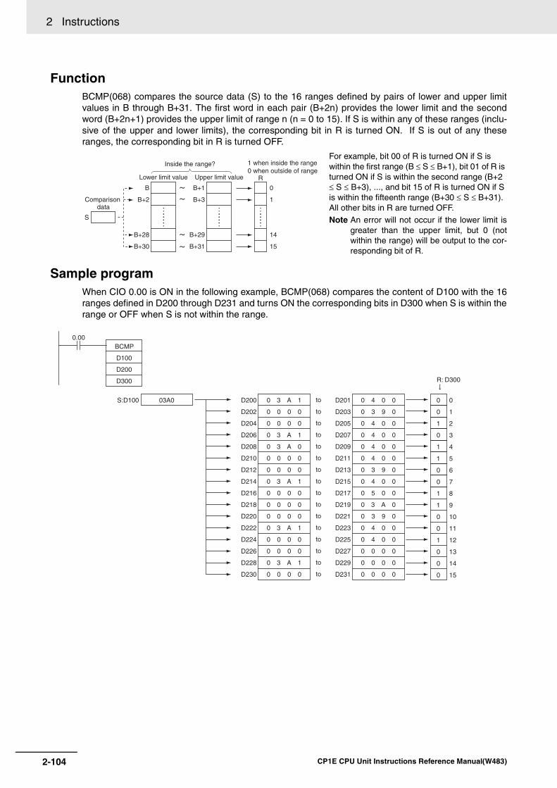
2 Instructions
FunctionBCMP(068) compares the source data (S) to the 16 ranges defined by pairs of lower and upper limitvalues in B through B+31. The first word in each pair (B+2n) provides the lower limit and the secondword (B+2n+1) provides the upper limit of range n (n = 0 to 15). If S is within any of these ranges (inclu-sive of the upper and lower limits), the corresponding bit in R is turned ON. If S is out of any theseranges, the corresponding bit in R is turned OFF.
Sample programWhen CIO 0.00 is ON in the following example, BCMP(068) compares the content of D100 with the 16ranges defined in D200 through D231 and turns ON the corresponding bits in D300 when S is within therange or OFF when S is not within the range.
For example, bit 00 of R is turned ON if S is within the first range (B ≤ S ≤ B+1), bit 01 of R is turned ON if S is within the second range (B+2 ≤ S ≤ B+3), ..., and bit 15 of R is turned ON if S is within the fifteenth range (B+30 ≤ S ≤ B+31). All other bits in R are turned OFF.Note An error will not occur if the lower limit is
greater than the upper limit, but 0 (notwithin the range) will be output to the cor-responding bit of R.
B
B+2
B+28
B+30
S
B+1
B+3
B+29
B+31
0
1
14
15
R
Inside the range?
Lower limit value Upper limit value
1 when inside the range0 when outside of range
Comparisondata
D201
D203
D205
D207
D209
D211
D213
D215
D217
D219
D221
D223
D225
D227
D229
D231
to
to
to
to
to
to
to
to
to
to
to
to
to
to
to
to
S:D100 03A0 D200
D202
D204
D206
D208
D210
D212
D214
D216
D218
D220
D222
D224
D226
D228
D230
R: D300
BCMP
D100
D200
D300
0.00
0 4 0 0
0 3 9 0
0 4 0 0
0 4 0 0
0 4 0 0
0 4 0 0
0 3 9 0
0 4 0 0
0 5 0 0
0 3 A 0
0 3 9 0
0 4 0 0
0 4 0 0
0 0 0 0
0 0 0 0
0 0 0 0
0
0
1
0
1
1
0
0
1
1
0
0
1
0
0
0
0
1
2
3
4
5
6
7
8
9
10
11
12
13
14
15
0 3 A 1
0 0 0 0
0 0 0 0
0 3 A 1
0 3 A 0
0 0 0 0
0 0 0 0
0 3 A 1
0 0 0 0
0 0 0 0
0 0 0 0
0 3 A 1
0 0 0 0
0 0 0 0
0 3 A 1
0 0 0 0
2-104 CP1E CPU Unit Instructions Reference Manual(W483)
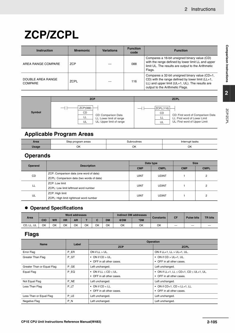
2 Instructions C
om
pariso
n In
structio
ns
2
ZC
P/Z
CP
L
ZCP/ZCPL
Applicable Program Areas
Operands
Operand Specifications
Flags
Instruction Mnemonic VariationsFunction
codeFunction
AREA RANGE COMPARE ZCP --- 088
Compares a 16-bit unsigned binary value (CD) with the range defined by lower limit LL and upper limit UL. The results are output to the Arithmetic Flags.
DOUBLE AREA RANGE COMPARE
ZCPL --- 116
Compares a 32-bit unsigned binary value (CD+1, CD) with the range defined by lower limit (LL+1, LL) and upper limit (UL+1, UL). The results are output to the Arithmetic Flags.
Symbol
ZCP ZCPL
Area Step program areas Subroutines Interrupt tasks
Usage OK OK OK
Operand Description Data type Size
CMP CMPL CMP CMPL
CDZCP: Comparison data (one word of data)
ZCPL: Comparison data (two words of data)UINT UDINT 1 2
LLZCP: Low limit
ZCPL: Low limit leftmost word numberUINT UDINT 1 2
ULZCP: High limit
ZCPL: High limit rightmost word numberUINT UDINT 1 2
Area Word addresses Indirect DM addresses
Constants CF Pulse bits TR bitsCIO WR HR AR T C DM @DM *DM
CD, LL, UL OK OK OK OK OK OK OK OK OK OK --- --- ---
Name LabelOperation
ZCP ZCPL
Error Flag P_ER ON if LL > UL. ON if LL+1, LL > UL+1, UL.
Greater Than Flag P_GT • ON if CD > UL.
• OFF in all other cases.
• ON if CD > UL+1, UL.
• OFF in all other cases.
Greater Than or Equal Flag P_GE Left unchanged. Left unchanged.
Equal Flag P_EQ • ON if LL ≤ CD ≤ UL.
• OFF in all other cases.
• ON if LL+1, LL ≤ CD+1, CD ≤ UL+1, UL.
• OFF in all other cases.
Not Equal Flag P_NE Left unchanged. Left unchanged.
Less Than Flag P_LT • ON if CD < LL.
• OFF in all other cases.
• ON if CD+1, CD < LL+1, LL.
• OFF in all other cases.
Less Than or Equal Flag P_LE Left unchanged. Left unchanged.
Negative Flag P_N Left unchanged. Left unchanged.
ZCP(088)
CD
LL
UL
CD: Comparison DataLL: Lower limit of rangeUL: Upper limit of range
ZCPL(116)
CD
LL
UL
CD: First word of Comparison DataLL: First word of Lower LimitUL: First word of Upper Limit
2-105CP1E CPU Unit Instructions Reference Manual(W483)

2 Instructions
Function ZCP
ZCP(088) compares the 16-bit signed binary data in CD with the range defined by LL and UL and out-puts the result to the Greater Than, Equals, and Less Than Flags in the Auxiliary Area. (The Less Thanor Equal, Greater Than or Equal, and Not Equal Flags are left unchanged.)
When CD > UL as shown below, the > flag turns ON.When LL ≤ CD ≤ UL, the = flag turns ON. When CD < LL, the < flag turns ON.
ZCPLZCPL(116) compares the 32-bit signed binary data in CD+1, CD with the range defined by LL+1, LLand UL+1, UL and outputs the result to the Greater Than, Equals, and Less Than Flags in the AuxiliaryArea. (The Less Than or Equal, Greater Than or Equal, and Not Equal Flags are left unchanged.)
When CD+1,CD > UL+1,UL as shown below, the > flag turns ON.When LL+1,LL ≤ CD+1, CD ≤ UL+1, UL, the = flag turns ON.When CD+1, CD < LL+1, LL, the < flag turns ON.
Precautions• When ZCP(088)/ZCPL(116) is executed, the result is reflected in the Arithmetic Flags. Control the
desired output or right-hand instruction with a branch from the same input condition that controlsZCP(088)/ZCPL(116), as shown in the following diagram.
ZCP(088)ResultFlag status
> = <
CD > UL ON OFF OFF
CD = UL OFF ON
LL < CD < UL
CD = LL
CD < LL OFF ON
ZCPL(116)ResultFlag status
> = <
CD+1, CD > UL+1, UL ON OFF OFF
CD+1, CD = UL+1, UL OFF ON
LL+1, LL < CD+1, CD < UL+1, UL
CD+1, CD = LL+1, LL
CD+1, CD < LL+1, LL OFF ON
A
ZCP
CD
LL
UL
Arithmetic Flag (Example: Equal Flag)
In this case, the Equals Flag and output A will be
turned ON when LL ≤ CD ≤ UL.
2-106 CP1E CPU Unit Instructions Reference Manual(W483)
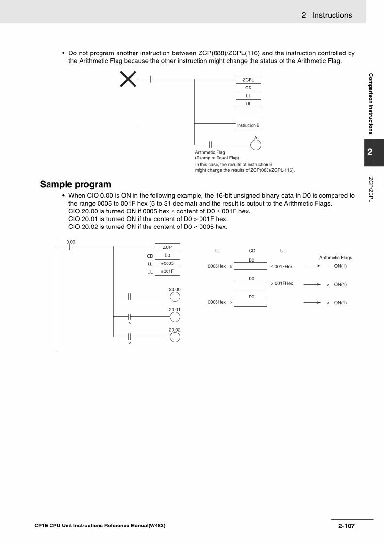
2 Instructions C
om
pariso
n In
structio
ns
2
ZC
P/Z
CP
L
• Do not program another instruction between ZCP(088)/ZCPL(116) and the instruction controlled bythe Arithmetic Flag because the other instruction might change the status of the Arithmetic Flag.
Sample program• When CIO 0.00 is ON in the following example, the 16-bit unsigned binary data in D0 is compared to
the range 0005 to 001F hex (5 to 31 decimal) and the result is output to the Arithmetic Flags.CIO 20.00 is turned ON if 0005 hex ≤ content of D0 ≤ 001F hex.CIO 20.01 is turned ON if the content of D0 > 001F hex.CIO 20.02 is turned ON if the content of D0 < 0005 hex.
In this case, the results of instruction B might change the results of ZCP(088)/ZCPL(116).
A
ZCPL
CD
LL
UL
Arithmetic Flag(Example: Equal Flag)
Instruction B
20.00
0.00
>
20.01
=
20.02
<
ZCP
D0
#0005
#001F
CD
LL
UL
Arithmetic Flags
≤ 001FHex
D0
LL CD UL
= ON(1)
D0> ON(1)
D0< ON(1)
> 001FHex
0005Hex ≤
0005Hex >
2-107CP1E CPU Unit Instructions Reference Manual(W483)

2 Instructions
Data Movement Instructions
MOV/MOVL/MVN
Applicable Program Areas
Operands
Operand Specifications
Flags
Instruction Mnemonic VariationsFunction
codeFunction
MOVE MOV@MOV, !MOV,
!@MOV021 Transfers a word of data to the specified word.
DOUBLE MOVE MOVL @MOVL 498 Transfers two words of data to the specified words.
MOVE NOT MVN @MVN 022Transfers the complement of a word of data to the specified word.
Symbol
MOV MOVL
MVN
Area Step program areas Subroutines Interrupt tasks
Usage OK OK OK
Operand Description Data type Size
MOV / MVN MOVL MOV / MVN MOVL
SMOV / MVN: Source
MOVL: First source wordWORD DWORD 1 2
DMOV / MVN: Destination
MOVL: First destination wordWORD DWORD 1 2
Area Word addresses Indirect DM addresses
Constants CF Pulse bits TR bitsCIO WR HR AR T C DM @DM *DM
SOK OK OK OK OK OK OK OK OK
OK--- --- ---
D ---
Name Label Operation
Error Flag P_ER OFF
Equal Flag P_EQ • ON if the data being transferred (D) is 0.
• OFF in all other cases.
Negative Flag P_N • ON if the leftmost bit of the data being transferred (D) is 1.
• OFF in all other cases.
MOV(021)
S
D
S: Source
D: Destination
MOVL(498)
S
D
S: First source word
D: First destinationword
MVN(022)
S
D
S: Source
D: Destination
2-108 CP1E CPU Unit Instructions Reference Manual(W483)

2 Instructions D
ata Mo
vemen
t Instru
ction
s
2
MO
V/M
OV
L/MV
N
Function
PrecautionsMOV(021) has an immediate refreshing variation (!MOV(021)). A CPU Unit Built-in input bits can bespecified for S and external output bits can be specified for D. Input bits used for S will refreshed justbefore, and output bits used for D will be refreshed just after execution.
When CPU Unit Built-in input is specified for S, the value of S will be in-refreshed when the instructionis executed and transferred to D. When external output is specified for D, the value of S will be trans-ferred to D and immediately out-refreshed when the instruction is executed. It is also possible to in-refresh S and out-refresh D at the same time.
Sample programWhen CIO 0.00 is ON in the following example, the content of CIO 100 is copied to D100.
MOVTransfers S to D. If S is a constant, the valuecan be used for a data setting.
MOVLMOVL(498) transfers S+1 and S to D+1 andD. If S+1 and S are constants, the value canbe used for a data setting.
MVNMVN(022) inverts the bits in S and transfersthe result to D. The content of S is leftunchanged.
S+1
D+1
S
D
S
D
S
D
1 00 1
Bit status inverted.
MOV
100
D100
0.00
100CH D100
2-109CP1E CPU Unit Instructions Reference Manual(W483)

2 Instructions
When CIO 0.00 is ON in the following example, the content of D101 and D100 are copied to D201 andD200.
When CIO 0.00 is ON in the following example, the status of the bits in CIO 100 is inverted and theresult is copied to D100.
0.01
MOV
+1234
D11
0.02
MOV
-1234
D12
0.03
D10 1 28111215
3 40347
D11 0 48111215
D 20347
D12 F B8111215
2 E0347
MOV
#1234
D10
(Decimal 1234)
(Decimal -1234)
(Hexadecimal 1234)
MOVL
D100
D200
0.00
D100
D101
D200
D201
MVN
100
D100
0.00
100CH
D100
1101
D
1001
9
0010
2
0000
0
0010
2
0110
6
1101
D
1111
F
2-110 CP1E CPU Unit Instructions Reference Manual(W483)

2 Instructions D
ata Mo
vemen
t Instru
ction
s
2
MO
VB
MOVB
Applicable Program Areas
Operands
C: Control Word
Operand Specifications
Flags
Instruction Mnemonic VariationsFunction
codeFunction
MOVE BIT MOVB @MOVB 082 Transfers the specified bit.
Symbol
MOVB
Area Step program areas Subroutines Interrupt tasks
Usage OK OK OK
Operand Description Data type Size
S Source word or data WORD 1
C Control word UINT 1
D Destination word WORD 1
Area Word addresses Indirect DM addresses
Constants CF Pulse bits TR bitsCIO WR HR AR T C DM @DM *DM
S, COK OK OK OK OK OK OK OK OK
OK--- --- ---
D ---
Name Label Operation
Error Flag P_ER • ON if the rightmost and leftmost two digits of C are not within the specified range of 00 to 0F.
• OFF in all other cases.
MOVB(082)
S
C
D
S: Source word or data
C: Control word
D: Destination word
C m n
Source bit: 00 to 0F (0 to 15 decimal)
Destination bit: 00 to 0F (0 to 15 decimal)
07815
2-111CP1E CPU Unit Instructions Reference Manual(W483)

2 Instructions
Function
HintThe same word can be specified for both S and D to copy a bit within a word.
PrecautionsThe other bits in the destination word are left unchanged.
Sample programWhen CIO 0.00 is ON in the following example, the 5th bit of the source word (W0) is copied to the 12th
bit of the destination word (W100) in accordance with the control word’s value of 0C05.
MOVB(082) copies the specified bit (n) from Sto the specified bit (m) in D. C m n
Sn
Dm
MOVB
W0
D200
W100
0.00
S
C
D
D:W100
011415
S:W0
0151415
C:D200 0C 05
078
78
78
15
12
2-112 CP1E CPU Unit Instructions Reference Manual(W483)

2 Instructions D
ata Mo
vemen
t Instru
ction
s
2
MO
VD
MOVD
Applicable Program Areas
Operands
S: Source Word D: Destination Word
C: Control Word
Operand Specifications
Instruction Mnemonic VariationsFunction
codeFunction
MOVE DIGIT MOVD @MOVD 083Transfers the specified digit or digits. (Each digit is made up of 4 bits.)
Symbol
MOVB
Area Step program areas Subroutines Interrupt tasks
Usage OK OK OK
Operand Description Data type Size
S Source word or data WORD 1
C Control word UINT 1
D Destination word UINT 1
The source digits are read from right to left,wrapping back to the rightmost digit (digit 0) ifnecessary.
The destination digits are written from right toleft, wrapping back to the rightmost digit (digit0) if necessary.
Area Word addresses Indirect DM addresses
Constants CF Pulse bits TR bitsCIO WR HR AR T C DM @DM *DM
S, COK OK OK OK OK OK OK OK OK
OK--- --- ---
D ---
MOVD(083)
S
C
D
S: Source word or data
C: Control word
D: Destination word
S Digit 3 Digit 2
8111215
Digit 1 Digit 0
0347
D Digit 3 Digit 2
8111215
Digit 1 Digit 0
0347
15 8 011 37 412
C 0
First digit in S (m): 0 to 3
Number of digits (n): 0 to 30: 1 digit 1: 2 digits2: 3 digits3: 4 digits
First digit in D ( ): 0 to 3
Always 0.
n m
2-113CP1E CPU Unit Instructions Reference Manual(W483)
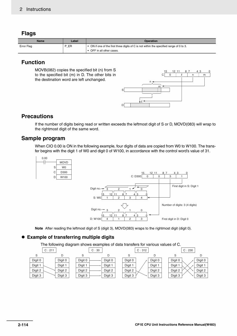
2 Instructions
Flags
Function
PrecautionsIf the number of digits being read or written exceeds the leftmost digit of S or D, MOVD(083) will wrap tothe rightmost digit of the same word.
Sample programWhen CIO 0.00 is ON in the following example, four digits of data are copied from W0 to W100. The trans-fer begins with the digit 1 of W0 and digit 0 of W100, in accordance with the control word’s value of 31.
Note After reading the leftmost digit of S (digit 3), MOVD(083) wraps to the rightmost digit (digit 0).
Example of transferring multiple digitsThe following diagram shows examples of data transfers for various values of C.
Name Label Operation
Error Flag P_ER • ON if one of the first three digits of C is not within the specified range of 0 to 3.
• OFF in all other cases.
MOVB(082) copies the specified bit (n) from Sto the specified bit (m) in D. The other bits inthe destination word are left unchanged.
Sm
n
DR
C 0 R
8111215n m
0347
MOVD
W0
D300
W100
0.00
S
C
D C D300 0 08111215
3 10347
D: W100 4 18111215
2 3
3 2 1 0
3 2 1 0
0347
S: W0 1 28111215
3 40347
Digit no.
Digit no.
First digit in D: Digit 0
Number of digits: 3 (4 digits)
First digit in S: Digit 1
S
C 211
D S
C 30
D S
C 312
D S
C 230
D
Digit 0
Digit 1
Digit 2
Digit 3
Digit 0
Digit 1
Digit 2
Digit 3
Digit 0
Digit 1
Digit 2
Digit 3
Digit 0
Digit 1
Digit 2
Digit 3
Digit 0
Digit 1
Digit 2
Digit 3
Digit 0
Digit 1
Digit 2
Digit 3
Digit 0
Digit 1
Digit 2
Digit 3
Digit 0
Digit 1
Digit 2
Digit 3
2-114 CP1E CPU Unit Instructions Reference Manual(W483)

2 Instructions D
ata Mo
vemen
t Instru
ction
s
2
XF
RB
XFRB
Applicable Program Areas
Operands
C: Control Word D: First destination Word
Note The source words and the destination words must be in the same data area respectively.
S: First Source Word
Operand Specifications
Flags
Instruction Mnemonic VariationsFunction
codeFunction
MULTIPLE BIT TRANSFER XFRB @XFRB 062Transfers the specified number of consecutive bits.
Symbol
XFRB
Area Step program areas Subroutines Interrupt tasks
Usage OK OK OK
Operand Description Data type Size
C Control word UINT 1
S First source word WORD Variable
D First destination word WORD Variable
Area Word addresses Indirect DM addresses
Constants CF Pulse bits TR bitsCIO WR HR AR T C DM @DM *DM
COK OK OK OK OK OK OK OK OK
OK--- --- ---
S, D ---
Name Label Operation
Error Flag P_ER OFF
XFRB(062)
C
S
D
C: Control word
S: First source word
D: First destination word
First bit in S ( ): 0 to F(0 to 15)
15 8 037 4
C n m
First bit in D (m): 0 to F(0 to 15)Number of bits (n):
00 to FF (0 to 255)
15 0D
to
D+16 max.
15 0S
to
S+16 max.
2-115CP1E CPU Unit Instructions Reference Manual(W483)

2 Instructions
Function
Hint• Up to 255 bits of data can be transferred per execution of XFRB(062).
• It is possible for the source words and destination words to overlap. By transferring data overlappingseveral words, the data can be packed more efficiently in the data area. (This is particularly usefulwhen handling position data for position control.)
• Since the source words and destination words can overlap, XFRB(062) can be combined withANDW(034) to shift m bits by n spaces.
Precautions• Be sure that the source words and destination words do not exceed the end of the data area.
• When the number of transfer bits (n of C) is 0, transfer does not take place.
• Bits in the destination words that are not overwritten by the source bits are left unchanged.
Sample programWhen CIO 0.00 is ON in the following example, the 20 bits beginning with W0.06 are copied to the 20bits beginning with W100.
XFRB(062) transfers up to 255 consecutivebits from the source words (beginning with bitl of S) to the destination words (beginning withbit m of D). The beginning bits and number of bits arespecified in C, as shown in the following dia-gram.
Sl
n
Dm
C n815
m l0347
XFRB
D100
W0
W100
0.00
C
S
D C:D100 1 4815
0 60347
S:W0W1
01234561415 78
D:W100W101
015
20 bits
2-116 CP1E CPU Unit Instructions Reference Manual(W483)

2 Instructions D
ata Mo
vemen
t Instru
ction
s
2
XF
ER
XFER
Applicable Program Areas
Operands
N: Number of WordsSpecifies the number of words to be transferred. The possible range for N is 0000 to FFFF (0 to65,535 decimal).
Operand Specifications
Flags
Instruction Mnemonic VariationsFunction
codeFunction
BLOCK TRANSFER XFER @XFER 070Transfers the specified number of consecutive words.
Symbol
XFER
Area Step program areas Subroutines Interrupt tasks
Usage OK OK OK
Operand Description Data type Size
N Number of words UINT 1
S First source word WORD Variable
D First destination word WORD Variable
Area Word addresses Indirect DM addresses
Constants CF Pulse bits TR bitsCIO WR HR AR T C DM @DM *DM
NOK OK OK OK OK OK OK OK OK
OK--- --- ---
S, D ---
Name Label Operation
Error Flag P_ER OFF
XFER(070)
N
S
D
N: Number of words
S: First source word
D: First destination word
15 0S
S+(N-1)
to
15 0D
D+(N-1)
to
2-117CP1E CPU Unit Instructions Reference Manual(W483)

2 Instructions
Function
Hint
Precautions• Be sure that the source words (S to S+N-1) and destination words (D to D+N-1) do not exceed the
end of the data area.
• Some time will be required to complete XFER(070) when a large number of words is being trans-ferred. Even if an interrupt occurs, execution of this instruction will not be interrupted and execution ofthe interrupt task will be started after execution of XFER(070) has been completed. If power is inter-rupted during execution of XFER(070), execution may not be completed, i.e., all of the specified datamay not be transferred.
Sample ProgramWhen CIO 0.00 is ON in the following example, the 10 words D100 through D109 are copied to D200through D209.
XFER(070) copies N words beginning with S(S to S+(N-1)) to the N words beginning withD (D to D+(N-1)).
• It is possible for the source words and desti-nation words to overlap, so XFER(070) canperform word-shift operations.
• The specified source and destination dataareas can overlap (word shift).
S
S+(N-1)
D
D+(N-1)
N words
D100
D109
D102
D111
XFER
&10
D100
D102
XFER
&1000
D0
D1000
XFER
&10
D100
D200
0.00
D100
D101
D102
D109
D200
D201
D202
D209
10 words
2-118 CP1E CPU Unit Instructions Reference Manual(W483)

2 Instructions D
ata Mo
vemen
t Instru
ction
s
2
BS
ET
BSET
Applicable Program Areas
Operands
St: Starting WordSpecifies the first word in the destination range.
E: End WordSpecifies the last word in the destination range.
Note St and E must be in the same data area.
Operand Specifications
Flags
Instruction Mnemonic VariationsFunction
codeFunction
BLOCK SET BSET @BSET 071Copies the same word to a range of consecutive words.
Symbol
BSET
Area Step program areas Subroutines Interrupt tasks
Usage OK OK OK
Operand Description Data type Size
S Source word WORD 1
St Starting word WORD Variable
E End word WORD Variable
Area Word addresses Indirect DM addresses
Constants CF Pulse bits TR bitsCIO WR HR AR T C DM @DM *DM
SOK OK OK OK OK OK OK OK OK
OK--- --- ---
St, E ---
Name Label Operation
Error Flag P_ER • ON if St is greater than E.
• OFF in all other cases.
BSET(071)
S
St
E
S: Source word
St: Starting word
E: End word
15
to
0St
E
2-119CP1E CPU Unit Instructions Reference Manual(W483)

2 Instructions
Function
Precautions• Some time will be required to complete BSET(071) when a large number of words is being set. Even
if an interrupt occurs, execution of this instruction will not be interrupted and execution of the interrupttask will be started after execution of BSET(071) has been completed. If power is interrupted duringexecution of BSET(071), execution may not be completed, i.e., all of the specified words may not beset. One BSET(071) instruction can be replaced with two BSET(071) instructions to help avoid thisproblem.
Sample programWhen CIO 0.00 is ON in the following example, the source data in D100 is copied to D200 throughD209.
BSET(071) copies the same source word (S)to all of the destination words in the range Stto E.
St
E
S
Destination wordsSource word
BSET
#0000
D1500
D1999
BSET
#0000
D1000
D1499
BSET
#0000
D1000
D1999
BSET
D100
D200
D209
0.00
S
St
ES D100 1 2 3 4 St:D200
D201
D202
D203
D204
D205
D206
D207
D208
E:D209
1 2 3 4
1 2 3 4
1 2 3 4
1 2 3 4
1 2 3 4
1 2 3 4
1 2 3 4
1 2 3 4
1 2 3 4
1 2 3 4
2-120 CP1E CPU Unit Instructions Reference Manual(W483)

2 Instructions D
ata Mo
vemen
t Instru
ction
s
2
XC
HG
XCHG
Applicable Program Areas
Operands
Operand Specifications
Flags
Function
Instruction Mnemonic VariationsFunction
codeFunction
DATA EXCHANGE XCHG @XCHG 073Exchanges the contents of the two specified words.
Symbol
XCHG
Area Step program areas Subroutines Interrupt tasks
Usage OK OK OK
Operand Description Data type Size
E1 First exchange word WORD 1
E2 Second exchange word WORD 1
Area Word addresses Indirect DM addresses
Constants CF Pulse bits TR bitsCIO WR HR AR T C DM @DM *DM
E1,E2 OK OK OK OK OK OK OK OK OK --- --- --- ---
Name Label Operation
Error Flag P_ER Unchanged
Equals Flag P_EQ Unchanged
Negative Flag P_N Unchanged
XCHG(073) exchanges the contents of E1 and E2.
XCHG(073)
E1
E2
E1: First exchange word
E2: Second exchange word
E2E1
2-121CP1E CPU Unit Instructions Reference Manual(W483)

2 Instructions
Hint
Sample program
To exchange 3 or more words, useXFER(070) to transfer the words to a third setof words (a buffer) as shown in this diagram.
When CIO 0.00 is ON in this example, the con-tent of D100 is exchanged with the content ofD200.
E1
E2
Buffer
1st XFER(070) operation
2nd XFER(070)operation
3rd XFER(070) operation
XCHG
D100
D200
0.00
D100 D200
D100 D200
1 2 3 4
A B C D 1 2 3 4
A B C D
2-122 CP1E CPU Unit Instructions Reference Manual(W483)

2 Instructions D
ata Mo
vemen
t Instru
ction
s
2
DIS
T
DIST
Applicable Program Areas
Operands
Bs: Destination Base Address
Of: OffsetThe offset can be any value from 0000 to FFFF (0 to 65,535 decimal).
Note Bs and Bs+Of must be in the same data area.
Operand Specifications
Flags
Instruction Mnemonic VariationsFunction
codeFunction
SINGLE WORD DISTRIBUTE DIST @DIST 080Transfers the source word to a destination word calculated by adding an offset value to the base address.
Symbol
DIST
Area Step program areas Subroutines Interrupt tasks
Usage OK OK OK
Operand Description Data type Size
S Source word WORD 1
Bs Destination base address WORD 1
Of Offset UINT 1
Area Word addresses Indirect DM addresses
Constants CF Pulse bits TR bitsCIO WR HR AR T C DM @DM *DM
S
OK OK OK OK OK OK OK OK OK
OK
--- --- ---Bs ---
Of OK
Name Label Operation
Error Flag P_ER OFF
Equals Flag P_EQ • ON if the source data is 0000.
• OFF in all other cases.
Negative Flag P_N • ON if the leftmost bit of the source data is 1.
• OFF in all other cases
DIST(080)
S
Bs
Of
S: Source word
Bs: Destination base address
Of: Offset
15 0
Bs
Bs+Of
2-123CP1E CPU Unit Instructions Reference Manual(W483)

2 Instructions
Function
HintThe same DIST(080) instruction can be used to distribute the source word to various words in the dataarea by changing the value of Of.
PrecautionsBe sure that the offset does not exceed the end of the data area, i.e., Bs and Bs+Of are in the samedata area.
Sample programWhen CIO 0.00 is ON in this example, the contents of D100 will be copied to D210 (D200 + 10) if thecontents of D300 is 10 (0A hexadecimal). The contents of D100 can be copied to other words by chang-ing the offset in D300.
DIST(080) copies S to the destination wordcalculated by adding Of to Bs. n
n
S
Bs+n
OfBs
DIST
D100
D200
D300
0.00S:D100
Bs:D200
D201
D210
S Copied by DIST(080).
Offset +10 words
4-digit hexadecimal
Bs
Of
Of:D300 0 0 0 A
2-124 CP1E CPU Unit Instructions Reference Manual(W483)
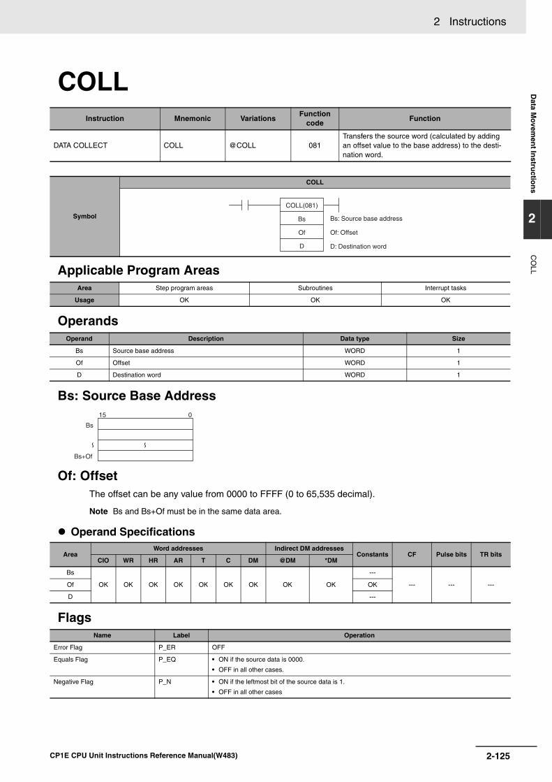
2 Instructions D
ata Mo
vemen
t Instru
ction
s
2
CO
LL
COLL
Applicable Program Areas
Operands
Bs: Source Base Address
Of: OffsetThe offset can be any value from 0000 to FFFF (0 to 65,535 decimal).
Note Bs and Bs+Of must be in the same data area.
Operand Specifications
Flags
Instruction Mnemonic VariationsFunction
codeFunction
DATA COLLECT COLL @COLL 081Transfers the source word (calculated by adding an offset value to the base address) to the desti-nation word.
Symbol
COLL
Area Step program areas Subroutines Interrupt tasks
Usage OK OK OK
Operand Description Data type Size
Bs Source base address WORD 1
Of Offset WORD 1
D Destination word WORD 1
Area Word addresses Indirect DM addresses
Constants CF Pulse bits TR bitsCIO WR HR AR T C DM @DM *DM
Bs
OK OK OK OK OK OK OK OK OK
---
--- --- ---Of OK
D ---
Name Label Operation
Error Flag P_ER OFF
Equals Flag P_EQ • ON if the source data is 0000.
• OFF in all other cases.
Negative Flag P_N • ON if the leftmost bit of the source data is 1.
• OFF in all other cases
COLL(081)
Bs
Of
D
Bs: Source base address
Of: Offset
D: Destination word
15 0
Bs
Bs+Of
2-125CP1E CPU Unit Instructions Reference Manual(W483)

2 Instructions
Function
HintThe same COLL(081) instruction can be used to collect data from various source words in the dataarea by changing the value of Of.
PrecautionsBe sure that the offset does not exceed the end of the data area, i.e., Bs and Bs+Of are in the samedata area.
Sample programWhen CIO 0.00 is ON in the following example, the contents of D110 (D100 + 10) will be copied toD300 if the content of D200 is 10 (0A hexadecimal). The contents of other words can be copied to D300by changing the offset in D200.
COLL(081) copies the source word (calculatedby adding Of to Bs) to the destination word. Bs
Bs+n
Of
D
n
n
COLL
D100
D200
D300
0.00
Bs
Of
D
D300
Bs:D100
D101
D110
D200 0 0 0 A
4-digit hexadecimal
Offset +10 words
Copied by COLL(081).
2-126 CP1E CPU Unit Instructions Reference Manual(W483)
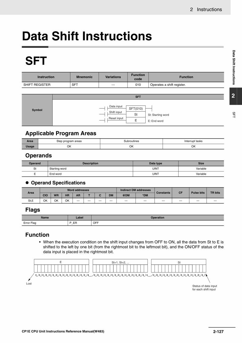
2 Instructions D
ata Sh
ift Instru
ction
s
2
SF
T
Data Shift Instructions
SFT
Applicable Program Areas
Operands
Operand Specifications
Flags
Function• When the execution condition on the shift input changes from OFF to ON, all the data from St to E is
shifted to the left by one bit (from the rightmost bit to the leftmost bit), and the ON/OFF status of thedata input is placed in the rightmost bit.
Instruction Mnemonic VariationsFunction
codeFunction
SHIFT REGISTER SFT --- 010 Operates a shift register.
Symbol
SFT
Area Step program areas Subroutines Interrupt tasks
Usage OK OK OK
Operand Description Data type Size
St Starting word UINT Variable
E End word UINT Variable
Area Word addresses Indirect DM addresses
Constants CF Pulse bits TR bitsCIO WR HR AR T C DM @DM *DM
St,E OK OK OK --- --- --- --- --- --- --- --- --- ---
Name Label Operation
Error Flag P_ER OFF
SFT(010)
St
E
Data input
Shift input
Reset inputSt: Starting word
E: End word
E
Status of data input for each shift input
Lost
St+1, St+2, ... St
2-127CP1E CPU Unit Instructions Reference Manual(W483)

2 Instructions
Precautions• Do not use more than one SFT(010) instructions with overlapping shift words. The results will not be
dependable.
• St and E must be in the same data area.
• The bit data shifted out of the shift register is discarded.
• When the reset input turns ON, all bits in the shift register from the rightmost designated word (St) tothe leftmost designated word (E) will be reset (i.e., set to 0). The reset input takes priority over otherinputs.
• St must be less than or equal to E, but even when St is set to greater than E an error will not occurand one word of data in St will be shifted.
Sample program Shift Register Exceeding 16 Bits
The following example shows a 48-bit shift register using words CIO 128 to CIO 130. A 1-s clock pulseis used so that the execution condition produced by CIO 0.05 is shifted into a 3-word register betweenCIO 128.00 and CIO 130.15 every second.
i
SFT
128
130
0.05
0.06
1s (1-s clock)
Reset
Shift input
Data input
015 015 0151 1 114 14 14
E: 130CH 129CH 128CH
Lost
Contents of 0.05
St+1: St:
2-128 CP1E CPU Unit Instructions Reference Manual(W483)

2 Instructions D
ata Sh
ift Instru
ction
s
2
SF
TR
SFTR
Applicable Program Areas
Operands
C: Control Word
Note St and E must be in the same data area.
Operand Specifications
Flags
Instruction Mnemonic VariationsFunction
codeFunction
REVERSIBLE SHIFT REGIS-TER
SFTR @SFTR 084Creates a shift register that shifts data to either the right or the left.
Symbol
SFTR
Area Step program areas Subroutines Interrupt tasks
Usage OK OK OK
Operand Description Data type Size
C Control word UINT 1
St Starting word UINT Variable
E End word UINT Variable
Area Word addresses Indirect DM addresses
Constants CF Pulse bits TR bitsCIO WR HR AR T C DM @DM *DM
C,St,E OK OK OK OK OK OK OK OK OK --- --- --- ---
Name Label Operation
Error Flag P_ER • ON when St is greater than E.
• OFF in all other cases.
Carry Flag P_CY • ON when 1 is shifted into it.
• OFF when 0 is shifted into it.
• OFF when reset is set to 1.
SFTR(084)
C
St
E
C: Control word
St: Starting word
E: End word
15 14 13 12
Data input
Reset
Shift input
Shift direction1 (ON): Left0 (OFF): Right
2-129CP1E CPU Unit Instructions Reference Manual(W483)

2 Instructions
Function
Note • The above shift operations are applicable when the reset bit (bit 15 of C) is set to OFF.
• When reset (bit 15 of C) turns ON all bits in the shift register, from St to E will be reset (i.e., set to 0).
Sample program• Shifting Data
If shift input W0.14 goes ON when CIO 0.00 is ON, and the reset bit W0.15 is OFF, words CIO 100through CIO 102 will shift one bit in the direction designated by W0.12 (e.g., 1: Right) and the contentsof input bit W0.13 will be shifted into the rightmost bit, CIO 100.00. The contents of CIO 102.15 will beshifted to the Carry Flag (CY).
• Resetting Data
If W0.14 is ON when CIO 0.00 is ON, and the reset bit, W0.15, is ON, words CIO 100 through CIO 102and the Carry Flag will be reset to OFF.
Controlling Data
When the execution condition ofthe shift input bit (bit 14 of C)changes to ON, all the data fromSt to E is moved in the designatedshift direction (designated by bit12 of C) by 1 bit, and the ON/OFFstatus of the data input is placedin the rightmost or leftmost bit.The bit data shifted out of the shiftregister is placed in the CarryFlag (CY)
All bits from St to E and the Carry Flag are set to 0 andno other data can be received when the reset input bit(bit 15 of C) is ON.
When the shift input bit (bit 14 of C) is ON, the contentsof the input bit (bit 13 of C) is shifted to bit 00 of the start-ing word, and each bit thereafter is shifted one bit to theleft. The status of bit 15 of the end word is shifted to theCarry Flag.
When the shift input bit (bit 14 of C) is ON, the contentsof the input bit (bit 13 of C) (I/O) is shifted to bit 15 on theend word, and each bit thereafter is shifted one bit to theright. The status of bit 00 of the starting word is shifted tothe Carry Flag.
015CY 015 015E St
C
015 CY015 015E St Shift direction
Data input
Data input
15141312
SFTR
W0
100
102
0.00
C
St
EC W0
015 14 13 12
110
15 0CY102 101 100
Data input: W0.13
Reset input bit: 0
Shift input bit: 1
Shift direction
015
0 0 0 0 0 0 0 0 0 0 0 0 0 0 0 0
CY
0
015CY
1/0
Data input
1/0
015 CYData input
Resetting Data
Shifting Data Left (from Rightmost to Leftmost Bit)
Shifting Data Right (from Leftmost to Rightmost Bit)
2-130 CP1E CPU Unit Instructions Reference Manual(W483)

2 Instructions D
ata Sh
ift Instru
ction
s
2
WS
FT
WSFT
Applicable Program Areas
Operands
Operand Specifications
Flags
Function
Precautions• St and E must be in the same data area.
• When large amounts of data are shifted, the instruction execution time is quite long. Be sure that thepower is not cut while WSFT(016) is being executed, causing the shift operation to stop halfwaythrough.
Instruction Mnemonic VariationsFunction
codeFunction
WORD SHIFT WSFT @WSFT 016 Shifts data between St and E in word units.
Symbol
WSFT
Area Step program areas Subroutines Interrupt tasks
Usage OK OK OK
Operand Description Data type Size
S Control word WORD 1
St Starting word UINT Variable
E End word UINT Variable
Area Word addresses Indirect DM addresses
Constants CF Pulse bits TR bitsCIO WR HR AR T C DM @DM *DM
SOK OK OK OK OK OK OK OK OK
OK--- --- ---
St,E ---
Name Label Operation
Error Flag P_ER • ON when St is greater than E.
• OFF in all other cases.
WSFT(016) shifts data from St toE in word units and the data fromthe source word S is places intoSt. The contents of E is lost.
WSFT(016)
S
St
E
S: Source word
St: Starting word
E: End word
015 015 015015
S
E St
Lost
2-131CP1E CPU Unit Instructions Reference Manual(W483)
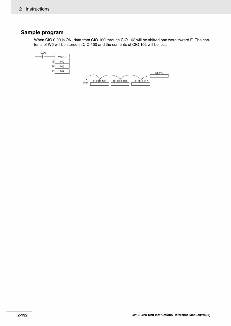
2 Instructions
Sample programWhen CIO 0.00 is ON, data from CIO 100 through CIO 102 will be shifted one word toward E. The con-tents of W0 will be stored in CIO 100 and the contents of CIO 102 will be lost.
i
WSFT
W0
100
102
0.00
S
St
E
E: CIO 100 St: CIO 101 St: CIO 102
St: W0
Lost
2-132 CP1E CPU Unit Instructions Reference Manual(W483)
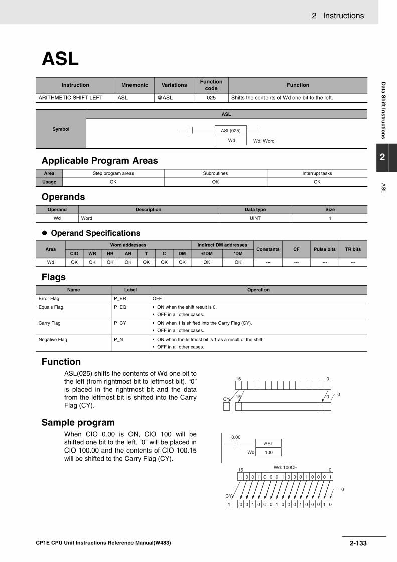
2 Instructions D
ata Sh
ift Instru
ction
s
2
AS
L
ASL
Applicable Program Areas
Operands
Operand Specifications
Flags
Function
Sample program
Instruction Mnemonic VariationsFunction
codeFunction
ARITHMETIC SHIFT LEFT ASL @ASL 025 Shifts the contents of Wd one bit to the left.
Symbol
ASL
Area Step program areas Subroutines Interrupt tasks
Usage OK OK OK
Operand Description Data type Size
Wd Word UINT 1
Area Word addresses Indirect DM addresses
Constants CF Pulse bits TR bitsCIO WR HR AR T C DM @DM *DM
Wd OK OK OK OK OK OK OK OK OK --- --- --- ---
Name Label Operation
Error Flag P_ER OFF
Equals Flag P_EQ • ON when the shift result is 0.
• OFF in all other cases.
Carry Flag P_CY • ON when 1 is shifted into the Carry Flag (CY).
• OFF in all other cases.
Negative Flag P_N • ON when the leftmost bit is 1 as a result of the shift.
• OFF in all other cases.
ASL(025) shifts the contents of Wd one bit tothe left (from rightmost bit to leftmost bit). “0”is placed in the rightmost bit and the datafrom the leftmost bit is shifted into the CarryFlag (CY).
When CIO 0.00 is ON, CIO 100 will beshifted one bit to the left. “0” will be placed inCIO 100.00 and the contents of CIO 100.15will be shifted to the Carry Flag (CY).
ASL(025)
Wd Wd: Word
0
0
15
015CY
ASL
100
0.00
Wd
015
1 0 0 1 0 0 0 1 0 0 0 1 0 0 0 1
0
CY
0 0 11 0 0 0 1 0 0 0 1 0 0 0 01
Wd: 100CH
2-133CP1E CPU Unit Instructions Reference Manual(W483)

2 Instructions
ASR
Applicable Program Areas
Operands
Operand Specifications
Flags
Function
Sample program
Instruction Mnemonic VariationsFunction
codeFunction
ARITHMETIC SHIFT RIGHT ASR @ASL 026 Shifts the contents of Wd one bit to the right.
Symbol
ASR
Area Step program areas Subroutines Interrupt tasks
Usage OK OK OK
Operand Description Data type Size
Wd Word UINT 1
Area Word addresses Indirect DM addresses
Constants CF Pulse bits TR bitsCIO WR HR AR T C DM @DM *DM
Wd OK OK OK OK OK OK OK OK OK --- --- --- ---
Name Label Operation
Error Flag P_ER OFF
Equals Flag P_EQ • ON when the shift result is 0.
• OFF in all other cases.
Carry Flag P_CY • ON when 1 is shifted into the Carry Flag (CY).
• OFF in all other cases.
Negative Flag P_N OFF
ASR(026) shifts the contents of Wdone bit to the right (from leftmost bit torightmost bit). “0” will be placed in theleftmost bit and the contents of therightmost bit will be shifted into theCarry Flag (CY).
When CIO 0.00 is ON, word CIO 100 willshift one bit to the right. “0” will be placed inCIO 100.15 and the contents of CIO 100.00will be shifted to the Carry Flag (CY).
Wd: Word
ASR(026)
Wd
0
0
15
CY
ASR
100
0.00
Wd
015
1 0 0 1 0 0 0 1 0 0 0 1 0 0 0 1
0
CY
0 1
Wd: 100CH
1 0 0 1 0 0 0 1 0 0 0 1 0 0 0
2-134 CP1E CPU Unit Instructions Reference Manual(W483)
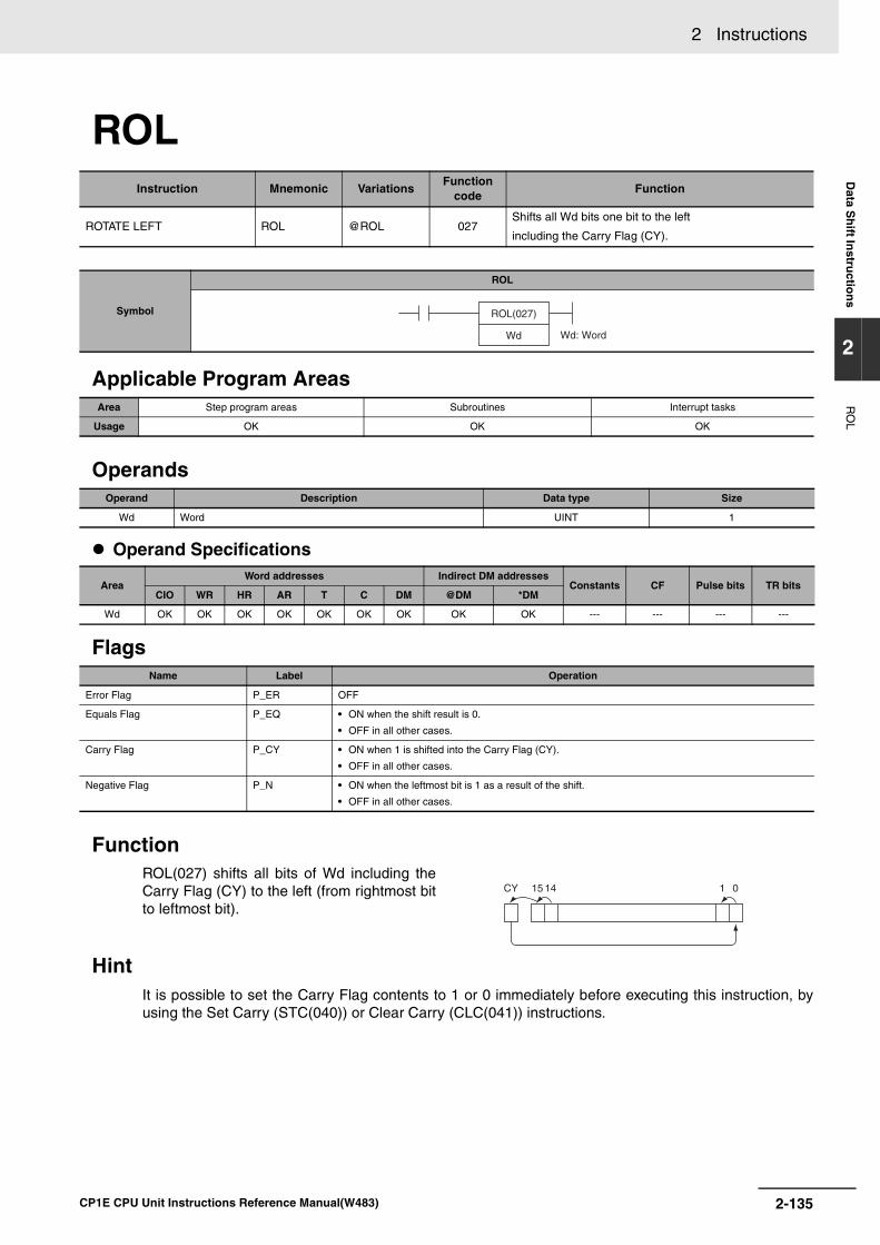
2 Instructions D
ata Sh
ift Instru
ction
s
2
RO
L
ROL
Applicable Program Areas
Operands
Operand Specifications
Flags
Function
HintIt is possible to set the Carry Flag contents to 1 or 0 immediately before executing this instruction, byusing the Set Carry (STC(040)) or Clear Carry (CLC(041)) instructions.
Instruction Mnemonic VariationsFunction
codeFunction
ROTATE LEFT ROL @ROL 027Shifts all Wd bits one bit to the left
including the Carry Flag (CY).
Symbol
ROL
Area Step program areas Subroutines Interrupt tasks
Usage OK OK OK
Operand Description Data type Size
Wd Word UINT 1
Area Word addresses Indirect DM addresses
Constants CF Pulse bits TR bitsCIO WR HR AR T C DM @DM *DM
Wd OK OK OK OK OK OK OK OK OK --- --- --- ---
Name Label Operation
Error Flag P_ER OFF
Equals Flag P_EQ • ON when the shift result is 0.
• OFF in all other cases.
Carry Flag P_CY • ON when 1 is shifted into the Carry Flag (CY).
• OFF in all other cases.
Negative Flag P_N • ON when the leftmost bit is 1 as a result of the shift.
• OFF in all other cases.
ROL(027) shifts all bits of Wd including theCarry Flag (CY) to the left (from rightmost bitto leftmost bit).
Wd: Word
ROL(027)
Wd
015 14 1CY
2-135CP1E CPU Unit Instructions Reference Manual(W483)
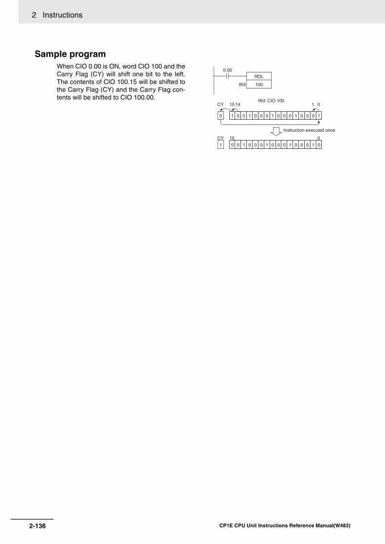
2 Instructions
Sample programWhen CIO 0.00 is ON, word CIO 100 and theCarry Flag (CY) will shift one bit to the left.The contents of CIO 100.15 will be shifted tothe Carry Flag (CY) and the Carry Flag con-tents will be shifted to CIO 100.00.
ROL
100
0.00
Wd
015
0
CY
1 0 0 1 0 0 0 1 0 0 0 1 0 0 0 01
015 14 1CY
1 0 0 1 0 0 0 1 0 0 0 1 0 0 0 1
Instruction executed once
Wd: CIO 100
2-136 CP1E CPU Unit Instructions Reference Manual(W483)

2 Instructions D
ata Sh
ift Instru
ction
s
2
RO
R
ROR
Applicable Program Areas
Operands
Operand Specifications
Flags
Function
HintIt is possible to set the Carry Flag contents to 1 or 0 immediately before executing this instruction, byusing the Set Carry (STC(040)) or Clear Carry (CLC(041)) instructions.
Instruction Mnemonic VariationsFunction
codeFunction
ROTATE RIGHT ROR @ROR 028Shifts all Wd bits one bit to the right including the Carry Flag (CY).
Symbol
ROR
Area Step program areas Subroutines Interrupt tasks
Usage OK OK OK
Operand Description Data type Size
Wd Word UINT 1
Area Word addresses Indirect DM addresses
Constants CF Pulse bits TR bitsCIO WR HR AR T C DM @DM *DM
Wd OK OK OK OK OK OK OK OK OK --- --- --- ---
Name Label Operation
Error Flag P_ER OFF
Equals Flag P_EQ • ON when the shift result is 0.
• OFF in all other cases.
Carry Flag P_CY • ON when 1 is shifted into the Carry Flag (CY).
• OFF in all other cases.
Negative Flag P_N • ON when the leftmost bit is 1 as a result of the shift.
• OFF in all other cases.
ROR(028) shifts all bits of Wd including theCarry Flag (CY) to the right (from leftmost bitto rightmost bit).
Wd: Word
ROR(028)
Wd
015 14 1
Wd
CY
2-137CP1E CPU Unit Instructions Reference Manual(W483)
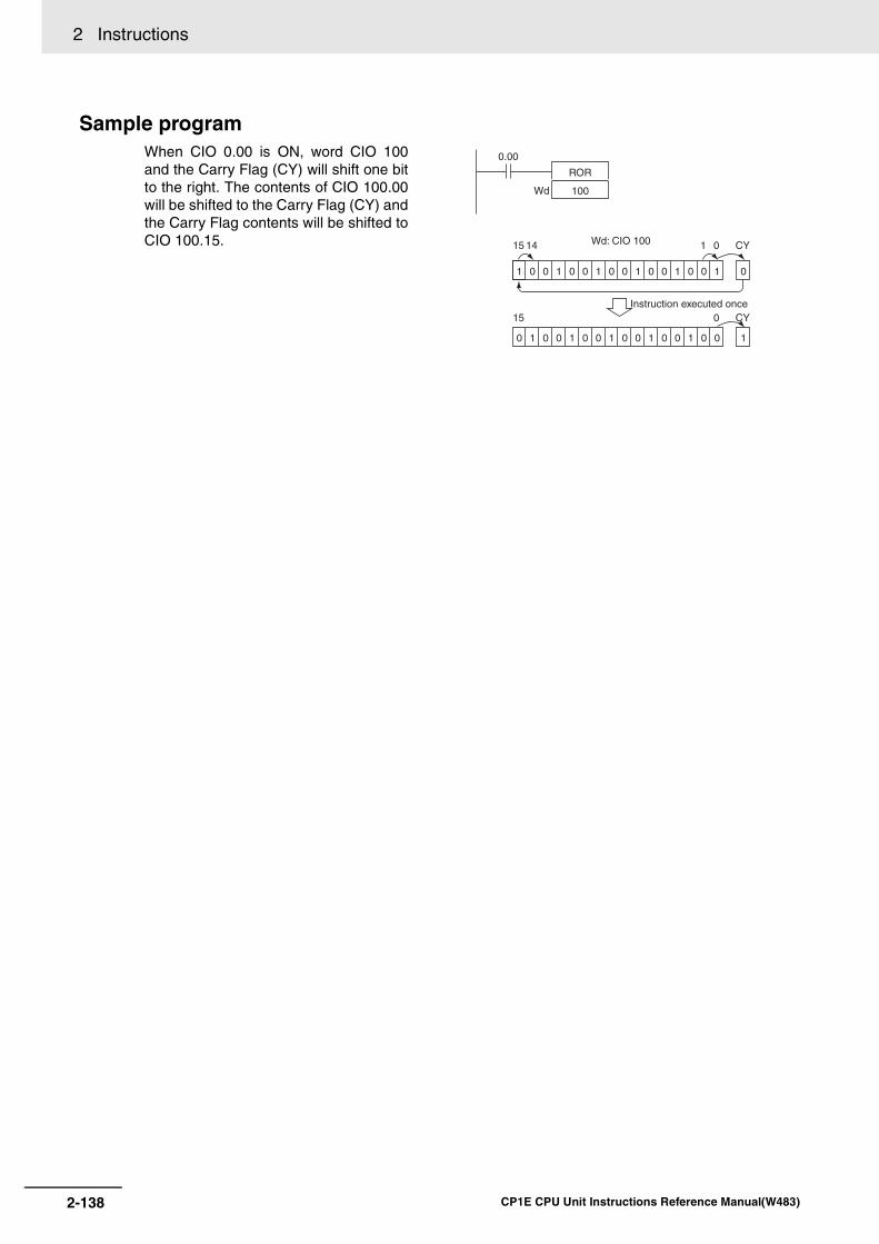
2 Instructions
Sample programWhen CIO 0.00 is ON, word CIO 100and the Carry Flag (CY) will shift one bitto the right. The contents of CIO 100.00will be shifted to the Carry Flag (CY) andthe Carry Flag contents will be shifted toCIO 100.15.
ROR
100
0.00
Wd
015
0 1 0 0 1 0 0 1 0 0 1 0 0 1 00
015 14 1
1 0 0 1 0 0 1 0 0 1 0 0 1 0 0 1 0
CY
1
CY
Instruction executed once
Wd: CIO 100
2-138 CP1E CPU Unit Instructions Reference Manual(W483)
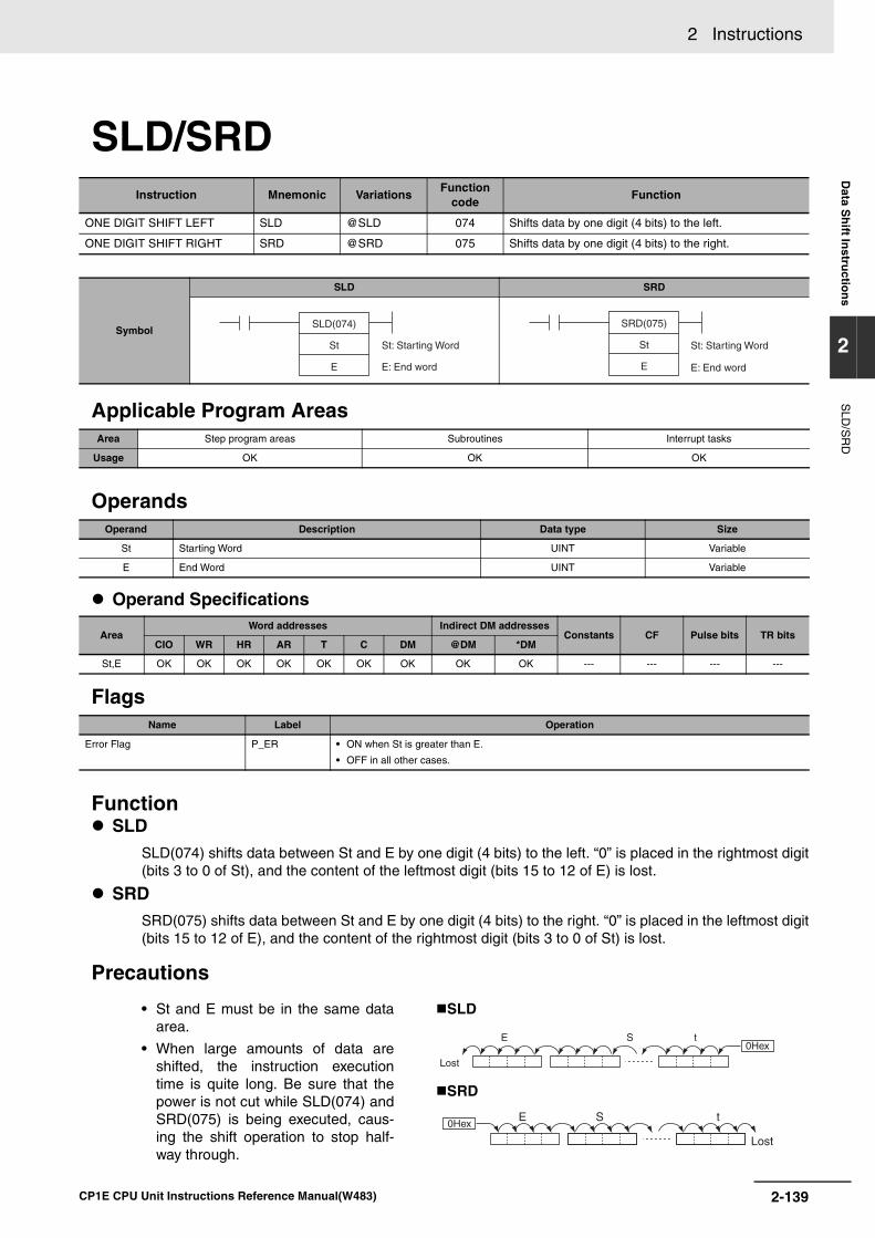
2 Instructions D
ata Sh
ift Instru
ction
s
2
SLD
/SR
D
SLD/SRD
Applicable Program Areas
Operands
Operand Specifications
Flags
Function SLD
SLD(074) shifts data between St and E by one digit (4 bits) to the left. “0” is placed in the rightmost digit(bits 3 to 0 of St), and the content of the leftmost digit (bits 15 to 12 of E) is lost.
SRDSRD(075) shifts data between St and E by one digit (4 bits) to the right. “0” is placed in the leftmost digit(bits 15 to 12 of E), and the content of the rightmost digit (bits 3 to 0 of St) is lost.
Precautions
Instruction Mnemonic VariationsFunction
codeFunction
ONE DIGIT SHIFT LEFT SLD @SLD 074 Shifts data by one digit (4 bits) to the left.
ONE DIGIT SHIFT RIGHT SRD @SRD 075 Shifts data by one digit (4 bits) to the right.
Symbol
SLD SRD
Area Step program areas Subroutines Interrupt tasks
Usage OK OK OK
Operand Description Data type Size
St Starting Word UINT Variable
E End Word UINT Variable
Area Word addresses Indirect DM addresses
Constants CF Pulse bits TR bitsCIO WR HR AR T C DM @DM *DM
St,E OK OK OK OK OK OK OK OK OK --- --- --- ---
Name Label Operation
Error Flag P_ER • ON when St is greater than E.
• OFF in all other cases.
• St and E must be in the same dataarea.
• When large amounts of data areshifted, the instruction executiontime is quite long. Be sure that thepower is not cut while SLD(074) andSRD(075) is being executed, caus-ing the shift operation to stop half-way through.
SLD
SRD
SLD(074)
St
E E: End word
St: Starting Word
SRD(075)
St
E E: End word
St: Starting Word
E S t
Lost
0Hex
E S
Lost
t0Hex
2-139CP1E CPU Unit Instructions Reference Manual(W483)
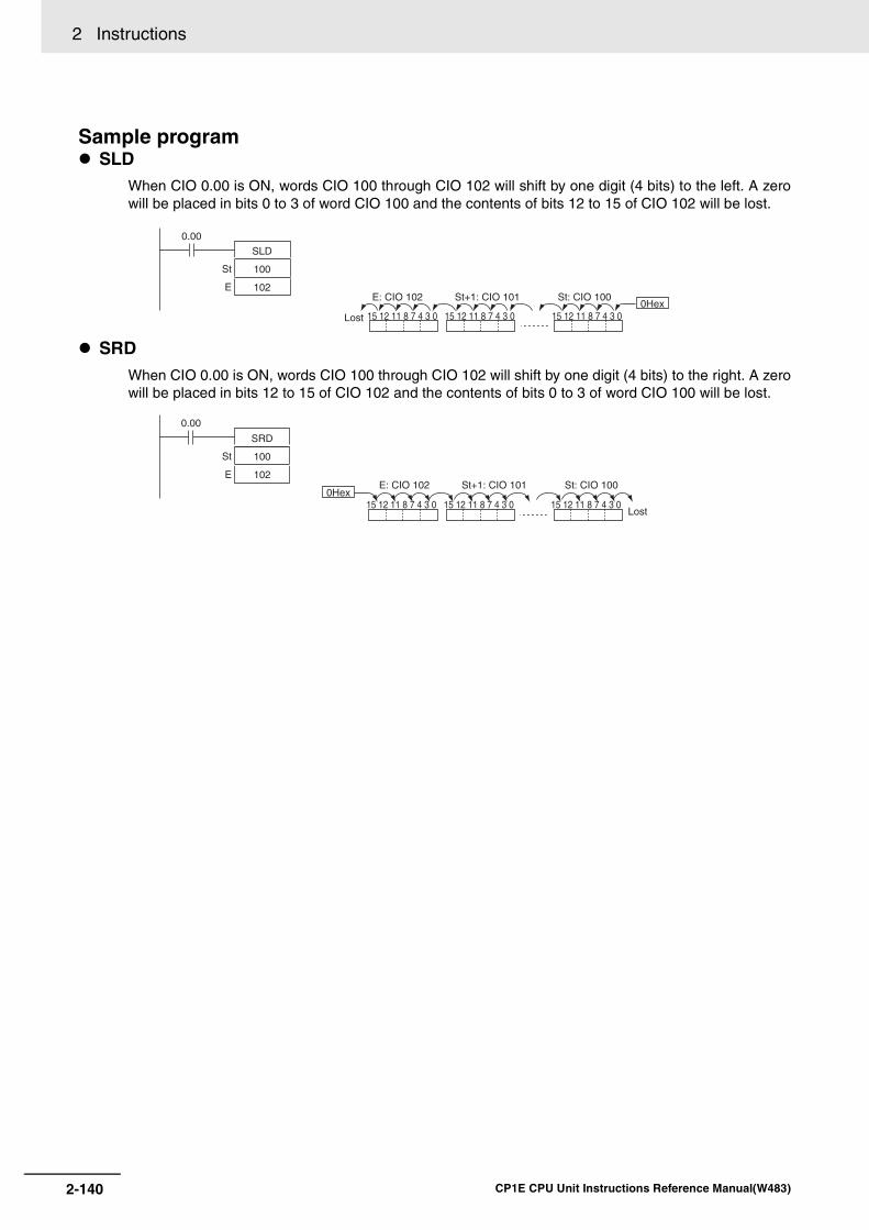
2 Instructions
Sample program SLD
When CIO 0.00 is ON, words CIO 100 through CIO 102 will shift by one digit (4 bits) to the left. A zerowill be placed in bits 0 to 3 of word CIO 100 and the contents of bits 12 to 15 of CIO 102 will be lost.
SRDWhen CIO 0.00 is ON, words CIO 100 through CIO 102 will shift by one digit (4 bits) to the right. A zerowill be placed in bits 12 to 15 of CIO 102 and the contents of bits 0 to 3 of word CIO 100 will be lost.
SLD
100
102
0.00
St
E
Lost0Hex
E: CIO 102 St+1: CIO 101 St: CIO 100
15 12 11 8 7 4 3 0 15 12 11 8 7 4 3 0 15 12 11 8 7 4 3 0
SRD
100
102
0.00
St
E
Lost
0HexE: CIO 102 St+1: CIO 101 St: CIO 100
15 12 11 8 7 4 3 0 15 12 11 8 7 4 3 0 15 12 11 8 7 4 3 0
2-140 CP1E CPU Unit Instructions Reference Manual(W483)
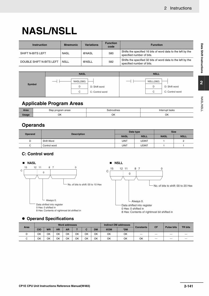
2 Instructions D
ata Sh
ift Instru
ction
s
2
NA
SL/N
SLL
NASL/NSLL
Applicable Program Areas
Operands
C: Control word
Operand Specifications
Instruction Mnemonic VariationsFunction
codeFunction
SHIFT N-BITS LEFT NASL @NASL 580Shifts the specified 16 bits of word data to the left by the specified number of bits.
DOUBLE SHIFT N-BITS LEFT NSLL @NSLL 582Shifts the specified 32 bits of word data to the left by the specified number of bits.
Symbol
NASL NSLL
Area Step program areas Subroutines Interrupt tasks
Usage OK OK OK
Operand Description Data type Size
NASL NSLL NASL NSLL
D Shift Word UINT UDINT 1 2
C Control word UINT UDINT 1 1
NASL NSLL
Area Word addresses Indirect DM addresses
Constants CF Pulse bits TR bitsCIO WR HR AR T C DM @DM *DM
D OK OK OK OK OK OK OK OK OK --- --- --- ---
C OK OK OK OK OK OK OK OK OK OK --- --- ---
NASL(580)
D
C
D: Shift word
C: Control word
NSLL(582)
D
C
D: Shift word
C: Control word
15 8 011 712C
0
No. of bits to shift: 00 to 10 Hex
Always 0.
Data shifted into register0 Hex: 0 shifted in 8 Hex: Contents of rightmost bit shifted in
15 8 011 712C
0
No. of bits to shift: 00 to 20 Hex
Always 0.Data shifted into register0 Hex: 0 shifted in 8 Hex: Contents of rightmost bit shifted in
2-141CP1E CPU Unit Instructions Reference Manual(W483)
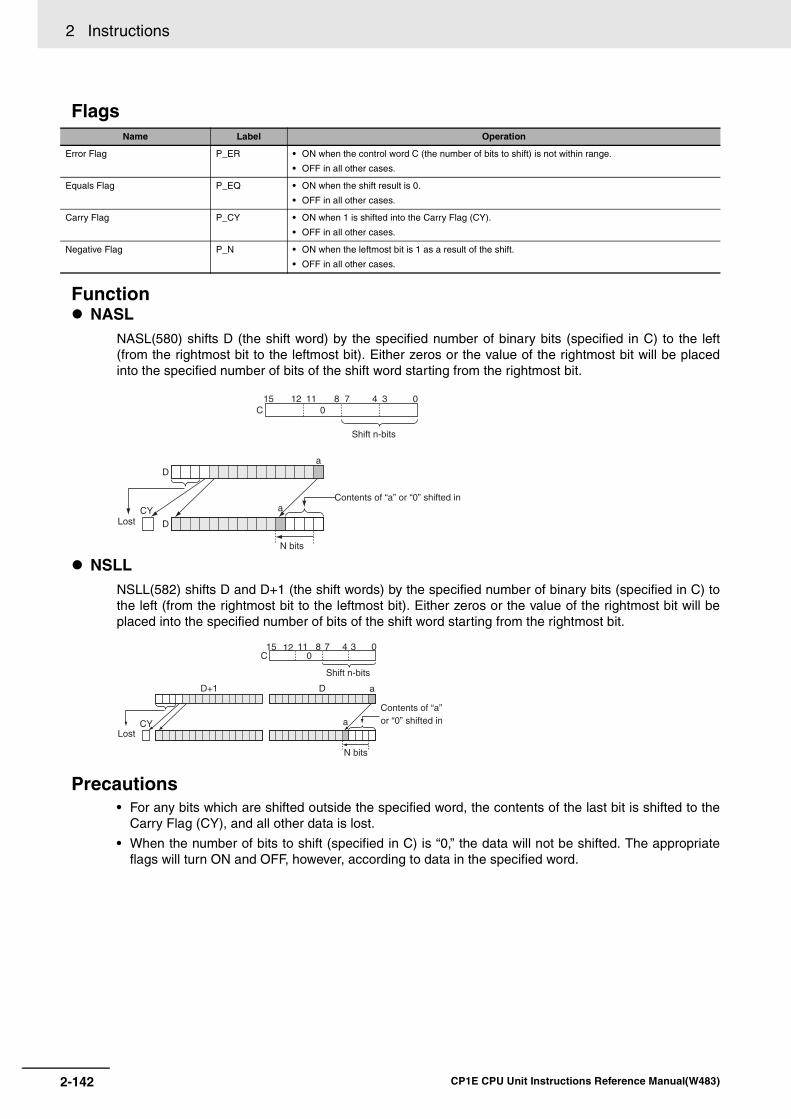
2 Instructions
Flags
Function NASL
NASL(580) shifts D (the shift word) by the specified number of binary bits (specified in C) to the left(from the rightmost bit to the leftmost bit). Either zeros or the value of the rightmost bit will be placedinto the specified number of bits of the shift word starting from the rightmost bit.
NSLLNSLL(582) shifts D and D+1 (the shift words) by the specified number of binary bits (specified in C) tothe left (from the rightmost bit to the leftmost bit). Either zeros or the value of the rightmost bit will beplaced into the specified number of bits of the shift word starting from the rightmost bit.
Precautions• For any bits which are shifted outside the specified word, the contents of the last bit is shifted to the
Carry Flag (CY), and all other data is lost.
• When the number of bits to shift (specified in C) is “0,” the data will not be shifted. The appropriateflags will turn ON and OFF, however, according to data in the specified word.
Name Label Operation
Error Flag P_ER • ON when the control word C (the number of bits to shift) is not within range.
• OFF in all other cases.
Equals Flag P_EQ • ON when the shift result is 0.
• OFF in all other cases.
Carry Flag P_CY • ON when 1 is shifted into the Carry Flag (CY).
• OFF in all other cases.
Negative Flag P_N • ON when the leftmost bit is 1 as a result of the shift.
• OFF in all other cases.
C 08111215 0347
Da
a
DCY
Shift n-bits
Contents of “a” or “0” shifted in
N bits
Lost
C 08111215 0347
D+1 D
CY
a
a
Shift n-bits
Contents of “a” or “0” shifted in
N bits
Lost
2-142 CP1E CPU Unit Instructions Reference Manual(W483)
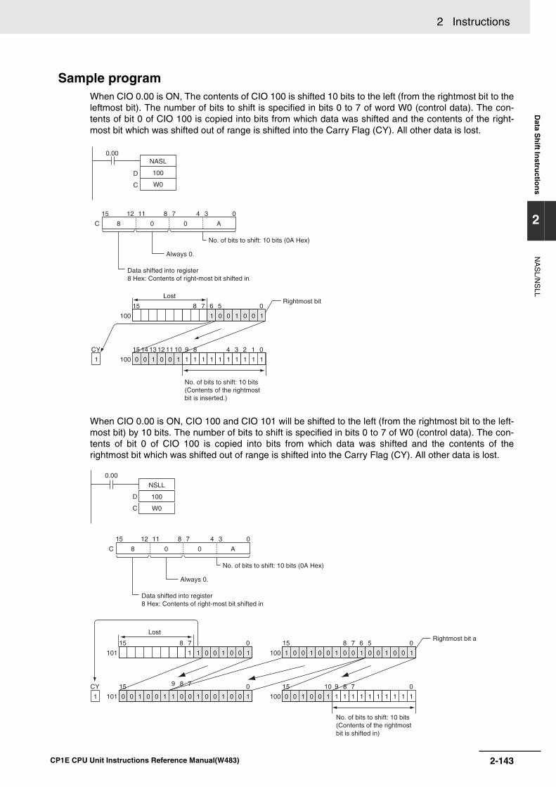
2 Instructions D
ata Sh
ift Instru
ction
s
2
NA
SL/N
SLL
Sample programWhen CIO 0.00 is ON, The contents of CIO 100 is shifted 10 bits to the left (from the rightmost bit to theleftmost bit). The number of bits to shift is specified in bits 0 to 7 of word W0 (control data). The con-tents of bit 0 of CIO 100 is copied into bits from which data was shifted and the contents of the right-most bit which was shifted out of range is shifted into the Carry Flag (CY). All other data is lost.
When CIO 0.00 is ON, CIO 100 and CIO 101 will be shifted to the left (from the rightmost bit to the left-most bit) by 10 bits. The number of bits to shift is specified in bits 0 to 7 of W0 (control data). The con-tents of bit 0 of CIO 100 is copied into bits from which data was shifted and the contents of therightmost bit which was shifted out of range is shifted into the Carry Flag (CY). All other data is lost.
NASL
100
W0
D
C
0.00
C 0
811
8
1215 07 4 3
0 A
No. of bits to shift: 10 bits (0A Hex)
Always 0.
Data shifted into register8 Hex: Contents of right-most bit shifted in
015
100
58 7 6
015 14 13 12 1011 4 39 8 2 1
100 1 1 1 1 1 1 1 1 11
CY
1
1 0 0 1 0 0 1
0 0 1 0 0 1
Rightmost bitLost
No. of bits to shift: 10 bits (Contents of the rightmost bit is inserted.)
NSLL
100
W0
0.00
D
C
C 0
811
8
1215 07 4 3
0 A
No. of bits to shift: 10 bits (0A Hex)
Always 0.
Data shifted into register8 Hex: Contents of right-most bit shifted in
015
101 11 0 0 1 0 0 1
0 0 1 0 0 1
8 7 015 8 7 6 5
015 9 8 7
101 1 0 0 1 0 0 1 0 10
CY
1
100 1 0 0 1 0 0 1
0 0 1 0 0 1
015 10 79 8
100 1 1 1 1 1 1 1 1 11
1 0 0 1 0 0 1 0 0
Rightmost bit aLost
No. of bits to shift: 10 bits (Contents of the rightmost bit is shifted in)
2-143CP1E CPU Unit Instructions Reference Manual(W483)

2 Instructions
NASR/NSRL
Applicable Program Areas
Operands
C: Control word
Operand Specifications
Instruction Mnemonic VariationsFunction
codeFunction
SHIFT N-BITS RIGHT NASR @NASR 581Shifts the specified 16 bits of word data to the right by the specified number of bits.
DOUBLE SHIFT N-BITS RIGHT
NSRL @NSRL 583Shifts the specified 32 bits of word data to the right by the specified number of bits.
Symbol
NASR NSRL
Area Step program areas Subroutines Interrupt tasks
Usage OK OK OK
Operand Description Data type Size
NASR NSRL NASR NSRL
D Shift Word UINT UDINT 1 2
C Control word UINT UDINT 1 1
NASR NSRL
Area Word addresses Indirect DM addresses
Constants CF Pulse bits TR bitsCIO WR HR AR T C DM @DM *DM
DOK OK OK OK OK OK OK OK OK
------ --- ---
C OK
NASR(581)
D
C C: Control word
D: Shift word
NSRL(583)
D
C C: Control word
D: Shift word
15 8 011 712C
0
No. of bits to shift: 00 to 10 Hex
Always 0.
Data shifted into register0 Hex: 0 shifted in 8 Hex: Contents of rightmost bit shifted in
15 8 011 712
C 0
No. of bits to shift: 00 to 20 Hex
Always 0.
Data shifted into register0 Hex: 0 shifted in 8 Hex: Contents of rightmost bit shifted in
2-144 CP1E CPU Unit Instructions Reference Manual(W483)

2 Instructions D
ata Sh
ift Instru
ction
s
2
NA
SR
/NS
RL
Flags
Function NASR
NASR(581) shifts D (the shift word) by the specified number of binary bits (specified in C) to the right(from the rightmost bit to the leftmost bit). Either zeros or the value of the rightmost bit will be placedinto the specified number of bits of the shift word starting from the rightmost bit.
NSRLNSRL(583) shifts D and D+1 (the shift words) by the specified number of binary bits (specified in C) tothe right (from the leftmost bit to the rightmost bit). Either zeros or the value of the rightmost bit will beplaced into the specified number of bits of the shift word starting from the rightmost bit.
Precautions• For any bits which are shifted outside the specified word, the contents of the last bit is shifted to the
Carry Flag (CY), and all other data is discarded.
• When the number of bits to shift (specified in C) is “0,” the data will not be shifted. The appropriateflags will turn ON and OFF, however, according to data in the specified word.
Name Label Operation
Error Flag P_ER • ON when the control word C (the number of bits to shift) is not within range.
• OFF in all other cases.
Equals Flag P_EQ • ON when the shift result is 0.
• OFF in all other cases.
Carry Flag P_CY • ON when 1 is shifted into the Carry Flag (CY).
• OFF in all other cases.
Negative Flag P_N • ON when the leftmost bit is 1 as a result of the shift.
• OFF in all other cases.
Da
a
DCY
Lost
N bits
Contents of “a” or “0” shifted in
C 08111215 0347
D+1 D
CY
a
a
Shift n-bits
Lost
Contents of “a” or “0” shifted in
2-145CP1E CPU Unit Instructions Reference Manual(W483)
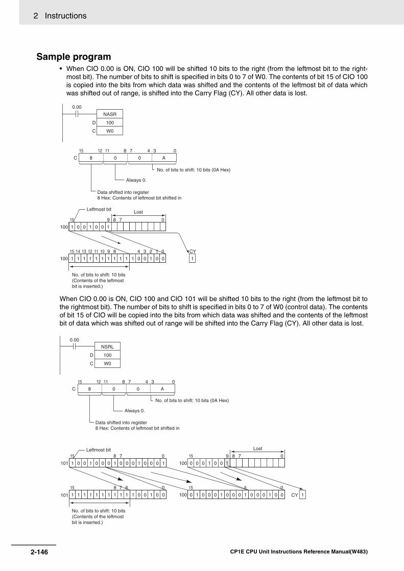
2 Instructions
Sample program• When CIO 0.00 is ON, CIO 100 will be shifted 10 bits to the right (from the leftmost bit to the right-
most bit). The number of bits to shift is specified in bits 0 to 7 of W0. The contents of bit 15 of CIO 100is copied into the bits from which data was shifted and the contents of the leftmost bit of data whichwas shifted out of range, is shifted into the Carry Flag (CY). All other data is lost.
.
When CIO 0.00 is ON, CIO 100 and CIO 101 will be shifted 10 bits to the right (from the leftmost bit tothe rightmost bit). The number of bits to shift is specified in bits 0 to 7 of W0 (control data). The contentsof bit 15 of CIO will be copied into the bits from which data was shifted and the contents of the leftmostbit of data which was shifted out of range will be shifted into the Carry Flag (CY). All other data is lost.
NASR
100
W0
0.00
D
C
C 0
811
8
1215 07 4 3
0 A
No. of bits to shift: 10 bits (0A Hex)
Data shifted into register8 Hex: Contents of leftmost bit shifted in
Always 0.
015
100 1
1 0 0 1 0 0
9 8 7
015 14 13 12 1011 4 39 8 2 1
1 0 0 1 0 0
100 1 1 1 1 1 1 1 1 11
CY
1
Leftmost bit Lost
No. of bits to shift: 10 bits (Contents of the leftmost bit is inserted.)
NSRL
100
W0
0.00
D
C
C 0
811
8
1215 07 4 3
0 A
No. of bits to shift: 10 bits (0A Hex)
Always 0.
Data shifted into register8 Hex: Contents of leftmost bit shifted in
015
101 1
0 0 0 1 0 0
8 7 015 8 79
15 8 7 6 0
101 0 1 0 0 0 1 0 0 10 CY 1
1001
1 0 0 1 0 0
06
1 0 0 1 0 0
1001 1 1 1 1 1 1 1 11
0 1 0 0 0 1 0 0 0
15
0 0 0 1 0 0
Leftmost bit Lost
No. of bits to shift: 10 bits (Contents of the leftmost bit is inserted.)
2-146 CP1E CPU Unit Instructions Reference Manual(W483)

2 Instructions In
cremen
t/Decrem
ent
Instru
ction
s
2
++
/++
L
Increment/Decrement Instructions
++/++L
Applicable Program Areas
Operands
Operand Specifications
Flags
Instruction Mnemonic VariationsFunction
codeFunction
INCREMENT BINARY ++ @++ 590Increments the 4-digit hexadecimal content of the specified word by 1.
DOUBLE INCREMENT BINARY
++L @++L 591Increments the 8-digit hexadecimal content of the specified words by 1.
Symbol
++ + +L
Area Step program areas Subroutines Interrupt tasks
Usage OK OK OK
Operand Description Data type Size
++ ++L ++ ++L
Wd++: Word++L: First word
UINT UDINT 1 2
AreaWord addresses Indirect DM addresses
Constants CF Pulse bits TR bitsCIO WR HR AR T C DM @DM *DM
Wd OK OK OK OK OK OK OK OK OK --- --- --- ---
Name Label Operation
Error Flag P_ER OFF
Equals Flag P_EQ • ON if the result is 0000/0000 0000 after execution.
• OFF in all other cases.
Carry Flag P_CY • ON if a digit in Wd/Wd+1 or Wd went from F to 0 during execution.
• OFF in all other cases.
Negative Flag P_N • ON if bit 15 of Wd/Wd+1 is ON after execution.
• OFF in all other cases.
Wd: Word
++(590)
Wd Wd: First word
++L(591)
Wd
2-147CP1E CPU Unit Instructions Reference Manual(W483)
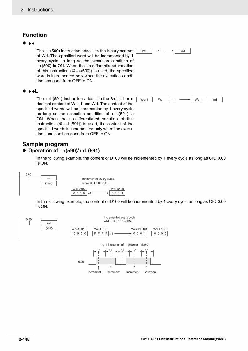
2 Instructions
Function
Sample program Operation of ++(590)/++L(591)
In the following example, the content of D100 will be incremented by 1 every cycle as long as CIO 0.00is ON.
In the following example, the content of D100 will be incremented by 1 every cycle as long as CIO 0.00is ON.
++The ++(590) instruction adds 1 to the binary contentof Wd. The specified word will be incremented by 1every cycle as long as the execution condition of++(590) is ON. When the up-differentiated variationof this instruction (@++(590)) is used, the specifiedword is incremented only when the execution condi-tion has gone from OFF to ON.
+ +LThe ++L(591) instruction adds 1 to the 8-digit hexa-decimal content of Wd+1 and Wd. The content of thespecified words will be incremented by 1 every cycleas long as the execution condition of ++L(591) isON. When the up-differentiated variation of thisinstruction (@++L(591)) is used, the content of thespecified words is incremented only when the execu-tion condition has gone from OFF to ON.
+1Wd Wd
WdWd+1 Wd+1 Wd+1
0 0 1 9
Wd: D100
0 0 1 A
Incremented every cycle while CIO 0.00 is ON.
Wd: D100
++
D100
+1
0.00
0.00
Wd+1: D101 Wd: D100 Wd+1: D101 Wd: D100
Increment Increment Increment Increment
: Execution of ++(590) or ++L(591)
Incremented every cycle while CIO 0.00 is ON.
+1
++L
D100
0.00
0 0 0 0 F F F F 0 0 0 1 0 0 0 0
2-148 CP1E CPU Unit Instructions Reference Manual(W483)

2 Instructions In
cremen
t/Decrem
ent
Instru
ction
s
2
++
/++
L
Operation of @++(590)/@++L(591)The up-differentiated variation is used in the following example, so the content of D100 will be incre-mented by 1 only when CIO 0.00 has gone from OFF to ON.
The up-differentiated variation is used in the following example, so the content of D101 and D100 will beincremented by 1 only when CIO 0.00 has gone from OFF to ON.
0 0 1 9
Wd: D100
0 0 1 A
Incremented every cycle while CIO 0.00 is ON.
Wd: D100
@++
D100
+1
0.00
0.00
Wd+1: D101 Wd: D100 Wd+1: D101 Wd: D100
Increment Increment
: Execution of @++(590) or @++L(591)
Incremented only for up-differentiation.
+1
@++L
D100
0.00
0 0 0 0 F F F F 0 0 0 1 0 0 0 0
2-149CP1E CPU Unit Instructions Reference Manual(W483)
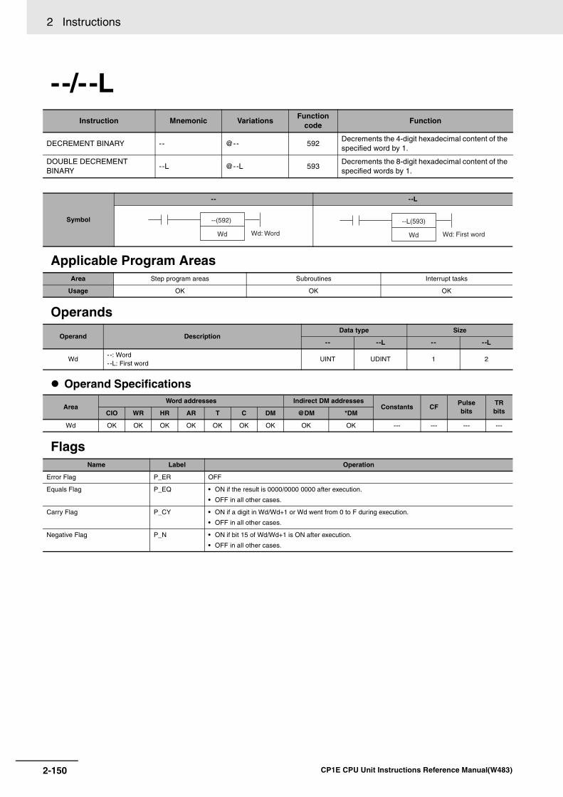
2 Instructions
--/--L
Applicable Program Areas
Operands
Operand Specifications
Flags
Instruction Mnemonic VariationsFunction
codeFunction
DECREMENT BINARY -- @-- 592Decrements the 4-digit hexadecimal content of the specified word by 1.
DOUBLE DECREMENT BINARY
--L @--L 593Decrements the 8-digit hexadecimal content of the specified words by 1.
Symbol
-- --L
Area Step program areas Subroutines Interrupt tasks
Usage OK OK OK
Operand Description Data type Size
-- --L -- --L
Wd--: Word--L: First word
UINT UDINT 1 2
Area Word addresses Indirect DM addresses
Constants CFPulse bits
TR bitsCIO WR HR AR T C DM @DM *DM
Wd OK OK OK OK OK OK OK OK OK --- --- --- ---
Name Label Operation
Error Flag P_ER OFF
Equals Flag P_EQ • ON if the result is 0000/0000 0000 after execution.
• OFF in all other cases.
Carry Flag P_CY • ON if a digit in Wd/Wd+1 or Wd went from 0 to F during execution.
• OFF in all other cases.
Negative Flag P_N • ON if bit 15 of Wd/Wd+1 is ON after execution.
• OFF in all other cases.
Wd: Word
--(592)
Wd Wd: First word
--L(593)
Wd
2-150 CP1E CPU Unit Instructions Reference Manual(W483)

2 Instructions In
cremen
t/Decrem
ent
Instru
ction
s
2
--/--L
Function
Sample program Operation of --(592)/--L(593)
The up-differentiated variation is used in the following example, so the content of D100 will be decre-mented by 1 only when CIO 0.00 has gone from OFF to ON.
In the following example, the 8-digit hexadecimal content of D101 and D100 will be decremented by 1every cycle as long as CIO 0.00 is ON.
--The --(592) instruction subtracts 1 from the binarycontent of Wd. The specified word will be decre-mented by 1 every cycle as long as the executioncondition of --(592) is ON. When the up-differenti-ated variation of this instruction (@ --(592)) is used,the specified word is decremented only when theexecution condition has gone from OFF to ON.
--LThe --L(593) instruction subtracts 1 from the 8-digithexadecimal content of Wd+1 and Wd. The contentof the specified words will be decremented by 1every cycle as long as the execution condition of --L(593) is ON. When the up-differentiated variation ofthis instruction (@--L(593)) is used, the content ofthe specified words is decremented only when theexecution condition has gone from OFF to ON.
-1Wd Wd
WdWd+1 Wd+1 Wd-1
0 0 2 0
Wd: D100
0 0 1 F
Decremented every cycle while CIO 0.00 is ON.
Wd: D100
--
D100
-1
0.00
0.00
Wd+1: D101 Wd: D100 Wd+1: D101 Wd: D100
Decrement Decrement Decrement Decrement
: Execution of --L(593)
Decremented every cycle while CIO 0.00 is ON.
-1
--L
D100
0.00
0 0 0 1 0 0 0 0 0 0 0 0 F F F F
2-151CP1E CPU Unit Instructions Reference Manual(W483)
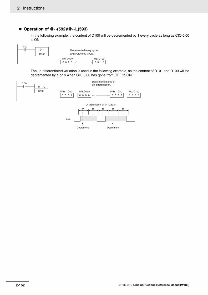
2 Instructions
Operation of @--(592)/@--L(593)In the following example, the content of D100 will be decremented by 1 every cycle as long as CIO 0.00is ON.
The up-differentiated variation is used in the following example, so the content of D101 and D100 will bedecremented by 1 only when CIO 0.00 has gone from OFF to ON.
0 0 2 0
Wd: D100
0 0 1 F
Decremented every cycle while CIO 0.00 is ON.
Wd: D100
@−−
D100
−1
0.00
0.00
Wd+1: D101 Wd: D100 Wd+1: D101 Wd: D100
Decrement Decrement
: Execution of @--L(593)
Decremented only for up-differentiation.
−1
@− −L
D100
0.00
0 0 0 1 0 0 0 0 0 0 0 0 F F F F
2-152 CP1E CPU Unit Instructions Reference Manual(W483)

2 Instructions In
cremen
t/Decrem
ent
Instru
ction
s
2
++
B/+
+B
L
++B/++BL
Applicable Program Areas
Operands
Operand Specifications
Flags
Instruction Mnemonic VariationsFunction
codeFunction
INCREMENT BCD ++B @++B 594Increments the 4-digit BCD content of the speci-fied word by 1.
DOUBLE INCREMENT BCD ++BL @++BL 595Increments the 8-digit BCD content of the speci-fied words by 1.
Symbol
++B + +BL
Area Step program areas Subroutines Interrupt tasks
Usage OK OK OK
Operand Description Data type Size
++ ++L ++ ++L
Wd++B: Word++BL: First word
WORD DWORD 1 2
Area Word addresses Indirect DM addresses
Constants CFPulse bits
TR bitsCIO WR HR AR T C DM @DM *DM
Wd OK OK OK OK OK OK OK OK OK --- --- --- ---
Name Label Operation
Error Flag P_ER • ON if the content of Wd/Wd+1 and Wd is not BCD.
• OFF in all other cases.
Equals Flag P_EQ • ON if the result is 0000/0000 0000 after execution.
• OFF in all other cases.
Carry Flag P_CY • ON if a digit in Wd/Wd+1 or Wd went from 9 to 0 during execution.
• OFF in all other cases.
Wd: Word
++B(594)
Wd Wd: First word
++BL(595)
Wd
2-153CP1E CPU Unit Instructions Reference Manual(W483)
2 Instructions
Function
Sample program Operation of ++B(594)/++BL(595)
In the following example, the BCD content of D100 will be incremented by 1 every cycle as long as CIO0.00 is ON.
In the following example, the 8-digit BCD content of D101 and D100 will be incremented by 1 everycycle as long as CIO 0.00 is ON.
++BThe ++B(594) instruction adds 1 to the BCD contentof Wd. The specified word will be incremented by 1every cycle as long as the execution condition of++B(594) is ON. When the up-differentiated variationof this instruction (@++B(594)) is used, the specifiedword is incremented only when the execution condi-tion has gone from OFF to ON.
+ +BLThe ++BL(595) instruction adds 1 to the 8-digit BCDcontent of Wd+1 and Wd. The content of the speci-fied words will be incremented by 1 every cycle aslong as the execution condition of ++BL(595) is ON.When the up-differentiated variation of this instruc-tion (@++BL(595)) is used, the content of the speci-fied words is incremented only when the executioncondition has gone from OFF to ON.
+1Wd Wd
WdWd+1 Wd+1 Wd+1
0 0 1 9
Wd: D100
0 0 2 0
Incremented every cycle while CIO 0.00 is ON.
Wd: D100
++B
D100
+1
0.00
0.00
Wd+1: D101 Wd: D100 Wd+1: D101 Wd: D100
Increment Increment Increment Increment
: Execution of ++B(594) / ++BL(595)
Incremented every cycle while CIO 0.00 is ON.
+1
++BL
D100
0.00
0 0 0 0 9 9 9 9 0 0 0 1 0 0 0 0
2-154 CP1E CPU Unit Instructions Reference Manual(W483)

2 Instructions In
cremen
t/Decrem
ent
Instru
ction
s
2
++
B/+
+B
L
Operation of @++B(594)/@++BL(595)The up-differentiated variation is used in the following example, so the content of D100 will be incre-mented by 1 only when CIO 0.00 has gone from OFF to ON.
The up-differentiated variation is used in the following example, so the BCD content of D101 and D100will be incremented by 1 only when CIO 0.00 has gone from OFF to ON.
0 0 1 9
Wd: D100
0 0 2 0
Incremented only forup-differentiation.
Wd: D100
@++B
D100
+1
0.00
0.00
Wd+1: D101 Wd: D100 Wd+1: D101 Wd: D100
Increment Increment
: Execution of @++B(594) or @++BL(595)
Incremented only for up-differentiation.
+1
@++BL
D100
0.00
0 0 0 0 9 9 9 9 0 0 0 1 0 0 0 0
2-155CP1E CPU Unit Instructions Reference Manual(W483)

2 Instructions
--B/--BL
Applicable Program Areas
Operands
Operand Specifications
Flags
Function
Instruction Mnemonic VariationsFunction
codeFunction
DECREMENT BCD --B @--B 596Decrements the 4-digit BCD content of the speci-fied word by 1.
DOUBLE DECREMENT BCD --BL @--BL 597Decrements the 8-digit BCD content of the speci-fied words by 1.
Symbol
--B --BL
Area Step program areas Subroutines Interrupt tasks
Usage OK OK OK
Operand Description Data type Size
-- --L -- --L
Wd--B: Word--BL: First word
WORD DWORD 1 2
Area Word addresses Indirect DM addresses
Constants CFPulse bits
TR bitsCIO WR HR AR T C DM @DM *DM
Wd OK OK OK OK OK OK OK OK OK --- --- --- ---
Name Label Operation
Error Flag P_ER • ON if the content of Wd/Wd+1 and Wd is not BCD.
• OFF in all other cases.
Equals Flag P_EQ • ON if the result is 0000/0000 0000 after execution.
• OFF in all other cases.
Carry Flag P_CY • ON if a digit in Wd/Wd+1 or Wd went from 0 to 9 during execution.
• OFF in all other cases.
--BThe --B(596) instruction subtracts 1 from the BCDcontent of Wd. The specified word will be decre-mented by 1 every cycle as long as the executioncondition of --B(596) is ON. When the up-differenti-ated variation of this instruction (@--B(596)) is used,the specified word is decremented only when the exe-cution condition has gone from OFF to ON.
--BLThe --BL(597) instruction subtracts 1 from the 8-digitBCD content of Wd+1 and Wd. The content of thespecified words will be decremented by 1 every cycleas long as the execution condition of --BL(597) is ON.When the up-differentiated variation of this instruction(@--BL(597)) is used, the content of the specifiedwords is decremented only when the execution condi-tion has gone from OFF to ON.
Wd: Word
--B(596)
Wd Wd: First word
--BL(597)
Wd
-1Wd Wd
WdWd+1 Wd+1 Wd-1
2-156 CP1E CPU Unit Instructions Reference Manual(W483)

2 Instructions In
cremen
t/Decrem
ent
Instru
ction
s
2
--B/--B
L
Sample program Operation of --B(596)/--BL(597)
In the following example, the BCD content of D100 will be decremented by 1 every cycle as long as CIO0.00 is ON.
In the following example, the 8-digit BCD content of D101 and D100 will be decremented by 1 everycycle as long as CIO 0.00 is ON.
Operation of @--B(596)/@--BL(597)The up-differentiated variation is used in the following example, so the BCD content of D100 will be dec-remented by 1 only when CIO 0.00 has gone from OFF to ON.
The up-differentiated variation is used in the following example, so the BCD content of D101 and D100will be decremented by 1 only when CIO 0.00 has gone from OFF to ON.
0 0 2 0
Wd: D100
0 0 1 9
Decremented every cycle while CIO 0.00 is ON.
Wd: D100
--B
D100
-1
0.00
0.00
Wd+1: D101 Wd: D100 Wd+1: D101 Wd: D100
Decrement Decrement Decrement Decrement
: Execution of --B(596) / --BL(597)
Decremented every cycle while CIO 0.00 is ON.
-1
--BL
D100
0.00
0 0 0 1 0 0 0 0 0 0 0 0 9 9 9 9
0 0 2 0
Wd: D100
0 0 1 9
Wd: D100
@--B
D100
-1
0.00
Decremented only for up-differentiation.
0.00
Wd+1: D101 Wd: D100 Wd+1: D101 Wd: D100
Decrement Decrement
: Execution of @--B(596) /@ --BL(597)
-1
@--BL
D100
0.00
0 0 0 1 0 0 0 0 0 0 0 0 9 9 9 9
Decremented only for up-differentiation.
2-157CP1E CPU Unit Instructions Reference Manual(W483)

2 Instructions
Symbol Math Instructions
+/+L
Applicable Program Areas
Operands
Operand Specifications
Instruction Mnemonic VariationsFunction
codeFunction
SIGNED BINARY ADD WITHOUT CARRY
+ @+ 400Adds 4-digit (single-word) hexadecimal data and/or constants.
DOUBLE SIGNED BINARY ADD WITHOUT CARRY
+L @+L 401Adds 8-digit (double-word) hexadecimal data and/or constants.
Symbol
+ +L
Area Step program areas Subroutines Interrupt tasks
Usage OK OK OK
Operand Description Data type Size
+ +L + +L
Au+: Augend word
+L: First augend wordINT DINT 1 2
Ad+: Addend word
+L: First addend wordINT DINT 1 2
R+: Result word
+L: First result wordINT DINT 1 2
AreaWord addresses Indirect DM addresses
Constants CF Pulse bits TR bitsCIO WR HR AR T C DM @DM *DM
Au, AdOK OK OK OK OK OK OK OK OK
OK--- --- ---
R ---
+(400)
R
Au
Ad
Au: Augend word
Ad: Addend word
R: Result word
+L(401)
R
Au
Ad
Au: 1st augend word
Ad: 1st addend word
R: 1st result word
2-158 CP1E CPU Unit Instructions Reference Manual(W483)
2 Instructions S
ymb
ol M
ath In
structio
ns
2
+/+
L
Flags
Function +
+(400) adds the binary values in Au and Ad and outputs the result to R.
+L+L(401) adds the binary values in Au and Au+1 and Ad and Ad+1 and outputs the result to R.
Sample program
Name LabelOperation
+ +L
Error Flag P_ER OFF OFF
Equals Flag P_EQ • ON when the result is 0.
• OFF in all other cases.
• ON when the result is 0.
• OFF in all other cases.
Carry Flag P_CY • ON when the addition results in a carry.
• OFF in all other cases.
• ON when the addition results in a carry.
• OFF in all other cases.
Overflow Flag P_OF • ON when the result of adding two positive num-bers is in the range 8000 to FFFF hex.
• OFF in all other cases.
• ON when the result of adding two positive num-bers is in the range 80000000 to FFFFFFFF hex.
• OFF in all other cases.
Underflow Flag P_UF • ON when the result of adding two negative num-bers is in the range 0000 to 7FFF hex.
• OFF in all other cases.
• ON when the result of adding two negative num-bers is in the range 00000000 to 7FFFFFFF hex.
• OFF in all other cases.
Negative Flag P_N • ON when the leftmost bit of the result is 1.
• OFF in all other cases.
• ON when the leftmost bit of the result is 1.
• OFF in all other cases.
+
CY R
Au
Ad
(Signed binary)
(Signed binary)
(Signed binary)CY will turn ON when there is a carry.
+
CY R+1 R
Au+1
Ad+1
Au
Ad
(Signed binary)
(Signed binary)
(Signed binary)CY will turn ON when there is a carry.
+0.00
+L
D100
D110
D120
0.00
When CIO 0.00 is ON in this example, D100 and D110 will be added as 4-digit signed binary values and the result will be output to D120.
When CIO 0.00 is ON, D101 and D100 and D111 and D110 will be added as 8-digit signed binary values and the result will be output to D121 and D120.
D100
D110
D120
2-159CP1E CPU Unit Instructions Reference Manual(W483)
2 Instructions
+C/+CL
Applicable Program Areas
Operands
Operand Specifications
Flags
Instruction Mnemonic VariationsFunction
codeFunction
SIGNED BINARY ADD WITH CARRY
+C @+C 402Adds 4-digit (single-word) hexadecimal data and/or constants with the Carry Flag (CY).
DOUBLE SIGNED BINARY ADD WITH CARRY
+CL @+CL 403Adds 8-digit (double-word) hexadecimal data and/or constants with the Carry Flag (CY).
Symbol
+C +CL
Area Step program areas Subroutines Interrupt tasks
Usage OK OK OK
Operand Description Data type Size
+C +CL +C +CL
Au+C: Augend word
+CL: First augend wordINT DINT 1 2
Ad+C: Addend word
+CL: First addend wordINT DINT 1 2
R+C: Result word
+CL: First result wordINT DINT 1 2
Area Word addresses Indirect DM addresses
Constants CF Pulse bits TR bitsCIO WR HR AR T C DM @DM *DM
Au, AdOK OK OK OK OK OK OK OK OK
OK--- --- ---
R ---
Name LabelOperation
+C +CL
Error Flag P_ER OFF OFF
Equals Flag P_EQ • ON when the addition result is 0.
• OFF in all other cases.
• ON when the result is 0.
• OFF in all other cases.
Carry Flag P_CY • ON when the addition results in a carry.
• OFF in all other cases.
• ON when the results in a carry.
• OFF in all other cases.
Overflow Flag P_OF • ON when the addition result of adding two positive numbers and CY is in the range 8000 to FFFF hex.
• OFF in all other cases.
• ON when the result of adding two positive num-bers and CY is in the range 80000000 to FFFFFFFF hex.
• OFF in all other cases.
Underflow Flag P_UF • ON when the addition result of adding two nega-tive numbers and CY is in the range 0000 to 7FFF hex.
• OFF in all other cases.
• ON when the result of adding two negative num-bers and CY is in the range 00000000 to 7FFFFFFF hex.
• OFF in all other cases.
Negative Flag P_N • ON when the leftmost bit of the result is 1.
• OFF in all other cases.
• ON when the leftmost bit of the result is 1.
• OFF in all other cases.
+C(402)
R
Au
Ad
Au: Augend word
Ad: Addend word
R: Result word
+CL(403)
Au
Ad
R
Au: 1st augend word
Ad: 1st addend word
R: 1st result word
2-160 CP1E CPU Unit Instructions Reference Manual(W483)
2 Instructions S
ymb
ol M
ath In
structio
ns
2
+C
/+C
L
Function +C
+C(402) adds the binary values in Au, Ad, and CY and outputs the result to R.
+CL+CL(403) adds the binary values in Au and Au+1, Ad and Ad+1, and CY and outputs the result to R.
Hint• To clear the Carry Flag (CY), execute the Clear Carry (CLC(041)) instruction.
Sample program
+ CY
RCY
Au
Ad
(Signed binary)
(Signed binary)
(Signed binary)CY will turn ON when there is a carry.
+ CY
RCY
Au+1
Ad+1
R+1
Au
Ad (Signed binary)
(Signed binary)
(Signed binary)CY will turn ON when there is a carry.
0.00
0.00
When CIO 0.00 is ON, D200, D210, and CY will be added as 4-digit signed binary values and the result will be output to D220.
When CIO 0.00 is ON, D201, D200, D211, D210, and CY will be added as 8-digit signed binary values, and the result will be output to D221 and D220.
+C
D200
D210
D220
+CL
D200
D210
D220
2-161CP1E CPU Unit Instructions Reference Manual(W483)

2 Instructions
+B/+BL
Applicable Program Areas
Operands
Operand Specifications
Flags
Instruction Mnemonic VariationsFunction
codeFunction
BCD ADD WITHOUT CARRY +B @+B 404Adds 4-digit (single-word) BCD data and/or con-stants.
DOUBLE BCD ADD WITHOUT CARRY
+BL @+BL 405Adds 8-digit (double-word) BCD data and/or con-stants.
Symbol
+B +BL
Area Step program areas Subroutines Interrupt tasks
Usage OK OK OK
Operand Description Data type Size
+B +BL +B +BL
Au+B: Augend word
+BL: First augend wordWORD DWORD 1 2
Ad+B: Addend word
+BL: First addend wordWORD DWORD 1 2
R+B: Result word
+BL: First result wordWORD DWORD 1 2
AreaWord addresses Indirect DM addresses
Constants CF Pulse bits TR bitsCIO WR HR AR T C DM @DM *DM
Au, AdOK OK OK OK OK OK OK OK OK
OK--- --- ---
R ---
Name LabelOperation
+B +BL
Error Flag P_ER • ON when Au is not BCD.
• ON when Ad is not BCD.
• OFF in all other cases.
• ON when Au, Au +1 is not BCD.
• ON when Ad, Ad +1 is not BCD.
• OFF in all other cases.
Equals Flag P_EQ • ON when the result is 0.
• OFF in all other cases.
• ON when the result is 0.
• OFF in all other cases.
Carry Flag P_CY • ON when the addition results in a carry.
• OFF in all other cases.
• ON when the addition results in a carry.
• OFF in all other cases.
+B(404)
R
Au
Ad
Au: Augend word
Ad: Addend word
R: Result word
+BL(405)
R
Au
Ad
Au: 1st augend word
Ad: 1st addend word
R: 1st result word
2-162 CP1E CPU Unit Instructions Reference Manual(W483)

2 Instructions S
ymb
ol M
ath In
structio
ns
2
+B
/+BL
Function +B
+B(404) adds the BCD values in Au and Ad and outputs the result to R.
+BL+BL(405) adds the BCD values in Au and Au+1 and Ad and Ad+1 and outputs the result to R, R+1.
Sample program
+
RCY
(BCD)
(BCD)
(BCD)
Au
Ad
CY will turn ON when there is a carry.
+
CY R
(BCD)
(BCD)
(BCD)R+1
Au+1
Ad+1
Au
Ad
CY will turn ON when there is a carry.
+B
D100
D110
D120
0.00
+BL
D100
D110
D120
0.00
When CIO 0.00 is ON in the following example, D100 and D110 will be added as 4-digit BCD values, and the result will be output to D120.
When CIO 0.00 is ON in the following example, D101 and D100 and D111 and D110 will be added as 8-digit BCD values, and the result will be output to D121 and D120.
2-163CP1E CPU Unit Instructions Reference Manual(W483)

2 Instructions
+BC/+BCL
Applicable Program Areas
Operands
Operand Specifications
Flags
Instruction Mnemonic VariationsFunction
codeFunction
BCD ADD WITH CARRY +BC @+BC 406Adds 4-digit (single-word) BCD data and/or con-stants with the Carry Flag (CY).
DOUBLE BCD ADD WITH CARRY
+BCL @+BCL 407Adds 8-digit (double-word) BCD data and/or con-stants with the Carry Flag (CY).
Symbol
+BC +BCL
Area Step program areas Subroutines Interrupt tasks
Usage OK OK OK
Operand Description Data type Size
+BC +BCL +BC +BCL
Au+BC: Augend word
+BCL: First augend wordWORD DWORD 1 2
Ad+BC: Addend word
+BCL: First addend wordWORD DWORD 1 2
R+BC: Result word
+BCL: First result wordWORD DWORD 1 2
AreaWord addresses Indirect DM addresses
Constants CF Pulse bits TR bitsCIO WR HR AR T C DM @DM *DM
Au, AdOK OK OK OK OK OK OK OK OK
OK--- --- ---
R ---
Name LabelOperation
+BC +BCL
Error Flag P_ER • ON when Au is not BCD.
• ON when Ad is not BCD.
• OFF in all other cases.
• ON when Au, Au +1 is not BCD.
• ON when Ad, Ad +1 is not BCD.
• OFF in all other cases.
Equals Flag P_EQ • ON when the result is 0.
• OFF in all other cases.
• ON when the result is 0.
• OFF in all other cases.
Carry Flag P_CY • ON when the addition results in a carry.
• OFF in all other cases.
• ON when the addition results in a carry.
• OFF in all other cases.
+BC(406)
R
Au
Ad
Au: Augend word
Ad: Addend word
R: Result word
+BCL(407)
R
Au
Ad
Au: 1st augend word
Ad: 1st addend word
R: 1st result word
2-164 CP1E CPU Unit Instructions Reference Manual(W483)

2 Instructions S
ymb
ol M
ath In
structio
ns
2
+B
C/+
BC
L
Function +BC
+BC(406) adds BCD values in Au, Ad, and CY and outputs the result to R.
+BCL+BCL(407) adds the BCD values in Au and Au+1, Ad and Ad+1, and CY and outputs the result to R,R+1.
Hint• To clear the Carry Flay (CY), execute the Clear Carry (CLC(041)) instruction.
Sample program
+ CY
RCY
(BCD)
(BCD)
(BCD)
Au
Ad
CY will turn ON when there is a carry.
+
R+1
CY
RCY
(BCD)
(BCD)
(BCD)
Au+1
Ad+1
Au
Ad
CY will turn ON when there is a carry.
+BC
D100
D110
D120
0.00
+BCL
D100
D110
D120
0.00
When CIO 0.00 is ON in the following example, D100, D110, and CY will be added as 4-digit BCD values, and the result will be output to D120.
When CIO 0.00 is ON in the following example, D101, D100, D111, D110, and CY will be added as 8-digit BCD values, and the result will be output to D121 and D120.
2-165CP1E CPU Unit Instructions Reference Manual(W483)

2 Instructions
–/–L
Applicable Program Areas
Operands
Operand Specifications
Flags
Instruction Mnemonic VariationsFunction
codeFunction
SIGNED BINARY SUBTRACT WITHOUT CARRY
– @– 410Subtracts 4-digit (single-word) hexadecimal data and/or constants.
DOUBLE SIGNED BINARY SUBTRACT WITHOUT CARRY
–L @–L 411Subtracts 8-digit (double-word) hexadecimal data and/or constants.
Symbol
– –L
Area Step program areas Subroutines Interrupt tasks
Usage OK OK OK
Operand Description Data type Size
– –L – –L
Mi–: Minuend word
–L: First minuend wordINT DINT 1 2
Su–: Subtrahend word
–L: First subtrahend wordINT DINT 1 2
R–: Result word
–L: First result wordINT DINT 1 2
Area Word addresses Indirect DM addresses
Constants CF Pulse bits TR bitsCIO WR HR AR T C DM @DM *DM
Mi, SuOK OK OK OK OK OK OK OK OK
OK--- --- ---
R ---
Name LabelOperation
– –L
Error Flag P_ER OFF OFF
Equals Flag P_EQ • ON when the result is 0.
• OFF in all other cases.
• ON when the result is 0.
• OFF in all other cases.
Carry Flag P_CY • ON when the subtraction results in a borrow.
• OFF in all other cases.
• ON when the subtraction results in a borrow.
• OFF in all other cases.
Overflow Flag P_OF • ON when the result of subtracting a negative num-ber from a positive number is in the range 8000 to FFFF hex.
• OFF in all other cases.
• ON when the result of subtracting a negative num-ber from a positive number is in the range 80000000 to FFFFFFFF hex.
• OFF in all other cases.
Underflow Flag P_UF • ON when the result of subtracting a negative num-ber from a positive number is in the range 0000 to 7FFF hex.
• OFF in all other cases.
• ON when the result of subtracting a positive num-ber from a negative number is in the range 00000000 to 7FFFFFFF hex.
• OFF in all other cases.
Negative Flag P_N • ON when the leftmost bit of the result is 1.
• OFF in all other cases.
• ON when the leftmost bit of the result is 1.
• OFF in all other cases.
R
Mi
Su
Mi: Minuend word
Su: Subtrahend word
R: Result word
-(410)
R
Mi
Su
Mi: Minuend word
Su: Subtrahend word
R: Result word
-L(410)
2-166 CP1E CPU Unit Instructions Reference Manual(W483)

2 Instructions S
ymb
ol M
ath In
structio
ns
2
–/–L
Function –
–(400) subtracts the binary values in Su from Mi and outputs the result to R. When the result is nega-tive, it is output to R as a 2’s complement.
–L–L(411) subtracts the binary values in Su and Su+1 from Mi and Mi+1 and outputs the result to R, R+1.When the result is negative, it is output to R and R+1 as a 2’s complement.
RCY
Mi
Su
(Signed binary)
(Signed binary)
(Signed binary)CY will turn ON when there is a borrow.
Su+1
CY R
Mi+1
R+1
Mi
Su
(Signed binary)
(Signed binary)
(Signed binary)CY will turn ON when there is a borrow.
2-167CP1E CPU Unit Instructions Reference Manual(W483)

2 Instructions
Hint• 2’s Complement
A 2’s complement is the value obtained by subtracting each binary digit from 1 and adding one to theresult. For example, the 2’s complement for 1101 is calculated as follows: 1111 (F hexadecimal) –1101 (D hexadecimal) + 1 (1 hexadecimal) = 0011 (3 hexadecimal). The 2’s complement for 3039(hexadecimal) is calculated as follows: FFFF (hexadecimal) – 3039 (hexadecimal) + 0001 (hexadeci-mal) – CFC7 (hexadecimal). Therefore, in case of 4-digit hexadecimal value, the 2’s complement canbe calculated as follows: FFFF (hexadecimal) – a (hexadecimal) + 0001 (hexadecimal) = b (hexadec-imal). To obtain the true number from the 2’s complement b (hexadecimal): a (hexadecimal) = 10000(hexadecimal) – b (hexadecimal). For example, to obtain the true number from the 2’s complementCFC7 (hexadecimal): 10000 (hexadecimal) – CFC7 = 3039.
20F55A10 - B8A360E3 = -97AE06D3. (Hexadecimal)
In this example, the eight-digit binary value in CIO 121 and CIO 120 is subtracted from the value in CIO201 and CIO 200, and the result is output in eight-digit binary to D101 and D100. If the result is nega-tive, the instruction at (2) will be executed, and the actual result will then be output to D101 and D100.
+165535
1
6553365535
Note 1.
2.
3.
4.
Example 1 Signed data Unsigned data
Example 2 Signed data Unsigned data
FFFF Hex0001 Hex
FFFE Hex 65534 Note 2
FFFD HexFFFF Hex
FFFE Hex 65534 Note 4
Carry Flag OFF
Negative Flag ON
Carry Flag OFF
Negative Flag ON
1
2 Note 1
1 3
2 Note 3
Since the Negative Flag is ON, the result (FFFE hex) is a negative value (2’s complement) and is thus -2.
Since the Carry Flag is OFF, the result (FFFE hex) is an unsigned positive value of 65534.
Since the Negative Flag is ON, the result (FFFE hex) is a negative value (2’s complement) and is thus -2.
Since the Carry Flag is ON, the result (FFFE hex) is a negative value (2’s complement) and becomes -2 when converted to a true value.
0.00
(1)
P_CY
P_CY(2)
RSET
21.00
SET
21.00
−L
200
120
D100
−L
#00000000
D100
D100
“−”display
2-168 CP1E CPU Unit Instructions Reference Manual(W483)

2 Instructions S
ymb
ol M
ath In
structio
ns
2
–/–L
Subtraction at (1)
Subtraction at (2)
Final Subtraction Result
Sample program
If the result of the subtraction is a negative number (Mi<Su or Mi+1, Mi <Su+1, Su), the result is outputas the 2’s complement and the Carry Flag (CY) will turn ON to indicate that the result of the subtractionis negative. To convert the 2’s complement to the true number, an instruction which subtracts the resultfrom 0 is necessary using the Carry Flag (CY) as an execution condition.
2
B
0
8
F
A
5
3
5
6
A
0
1
E
0
3
Mi+1: CIO 201
CY
Mi: CIO 200
Su+1: CIO 121 Su: CIO 120
6 8 5 1 F 9 2 D1
R+1: D101 R+1: D100 The Carry Flag (CY) is ON, so the result is subtracted from 0000 0000 to obtain the actual number.
0 0 0 0 0 0 0 0
CY
Su+1: D101 Su: D100
9 7 A E 0 6 D 31
R+1: D101 R+1: D100
6 8 5 1 F 9 2 D
CY
9 7 A E 0 6 D 31
R+1: D101 R+1: D100
6 8 5 1 F 9 2 D
Mi+1: CIO 201 Mi: CIO 200
2 0 F 5 5 A 1 0
Su+1: D101 Su: D100
The Carry Flag (CY) is turned ON, so the actual number is –97AE06D3. Because the content of D101 and D100 is negative, CY is used to turn ON CIO 21.00 to indicate this.
0.00When CIO 0.00 is ON in the following example, D110 will be subtracted from D100 as 4-digit signed binary values and the result will be output to D120.
0.00When CIO 0.00 is ON in the following example, D111 and D110 will be subtracted from D101 and D100 as 8-digit signed binary values and the result will be output to D121 and D120.
−
D100
D110
D120
−L
D100
D110
D120
2-169CP1E CPU Unit Instructions Reference Manual(W483)

2 Instructions
–C/–CL
Applicable Program Areas
Operands
Operand Specifications
Flags
Instruction Mnemonic VariationsFunction
codeFunction
SIGNED BINARY SUBTRACT WITH CARRY
–C @–C 412Subtracts 4-digit (single-word) hexadecimal data and/or constants with the Carry Flag (CY).
DOUBLE SIGNED BINARY SUBTRACT WITH CARRY
–CL @–CL 413Subtracts 8-digit (double-word) hexadecimal data and/or constants with the Carry Flag (CY).
Symbol
–C –CL
Area Step program areas Subroutines Interrupt tasks
Usage OK OK OK
Operand Description Data type Size
–C –CL –C –CL
Mi–C: Minuend word
–CL: First minuend wordINT DINT 1 2
Su–C: Subtrahend word
–CL: First subtrahend wordINT DINT 1 2
R–C: Result word
–CL: First result wordINT DINT 1 2
AreaWord addresses Indirect DM addresses
Constants CF Pulse bits TR bitsCIO WR HR AR T C DM @DM *DM
Mi, SuOK OK OK OK OK OK OK OK OK
OK--- --- ---
R ---
Name LabelOperation
–C –CL
Error Flag P_ER OFF OFF
Equals Flag P_EQ • ON when the subtraction result is 0.
• OFF in all other cases.
• ON when the result is 0.
• OFF in all other cases.
Carry Flag P_CY • ON when the subtraction results in a borrow.
• OFF in all other cases.
• ON when the results in a borrow.
• OFF in all other cases.
Overflow Flag P_OF • ON when the result of subtracting a negative num-ber and CY from a positive number is in the range 8000 to FFFF hex.
• OFF in all other cases.
• ON when the result of subtracting a negative num-ber and CY from a positive number is in the range 80000000 to FFFFFFFF hex.
• OFF in all other cases.
Underflow Flag P_UF • ON when the result of subtracting a positive num-ber and CY from a negative number is in the range 0000 to 7FFF hex.
• OFF in all other cases.
• ON when the result of subtracting a positive num-ber and CY from a negative number is in the range 00000000 to 7FFFFFFF hex.
• OFF in all other cases.
Negative Flag P_N • ON when the leftmost bit of the result is 1.
• OFF in all other cases.
• ON when the leftmost bit of the result is 1.
• OFF in all other cases.
R
Mi
Su
Mi: Minuend word
Su: Subtrahend word
R: Result word
–C(412) –CL(413)
R
Mi
Su
Mi: Minuend word
Su: Subtrahend word
R: Result word
2-170 CP1E CPU Unit Instructions Reference Manual(W483)
2 Instructions S
ymb
ol M
ath In
structio
ns
2
–C/–C
L
Function –C
–C(412) subtracts the binary values in Su and CY from Mi, and outputs the result to R. When the resultis negative, it is output to R as a 2’s complement.
–CL–CL(413) subtracts the binary values in Su and Su+1 and CY from Mi and Mi+1, and outputs the resultto R, R+1. When the result is negative, it is output to R, R+1 as a 2’s complement.
Hint• To clear the Carry Flag (CY), execute the Clear Carry (CLC(041)) instruction.
• 2’s ComplementA 2’s complement is the value obtained by subtracting each binary digit from 1 and adding one to theresult.
Example: The 2’s complement for the binary number 1101 is as follows:1111 (F hex) – 1101 (D hex) + 1 (1 hex) = 0011 (3 hex).
Example: The 2’s complement for the 4-digit hexadecimal number 3039 is as follows:FFFF hex - 3039 hex + 0001 hex = CFC7 hex.Accordingly, the 2’s complement for the 4-digit hexadecimal value “a” is as follows:FFFF hex – a hex + 0001 hex = b hex.And to obtain the true number “a” hex from the 2’s complement “b” hex:a hex + 10000 hex – b hex.
Example: To obtain the true number from the 2’s complement CFC& hex:10000 hex – CFC7 hex = 3039 hex.
Sample program
If the result of the subtraction is a negative number (Mi<Su or Mi+1, Mi <Su+1, Su), the result is outputas a 2’s complement. The Carry Flag (CY) will turn ON. To convert the 2’s complement to the true num-ber, a program which subtracts the result from 0 is necessary, as an input condition of the Carry Flag(CY). The Carry Flag turning ON thus indicates that the result of the subtraction is negative.
– CY
RCY
Mi
Su
(Signed binary)
(Signed binary)
(Signed binary)CY will turn ON when there is a borrow.
–
R+1
CY
RCY
Mi+1
Su+1
Mi
Su
(Signed binary)
(Signed binary)
(Signed binary)CY will turn ON when there is a borrow.
−C
D100
D110
D120
0.00When CIO 0.00 is ON in the following example, D110 and CY will be subtracted from D100 as 4-digit signed binary values and the result will be output to D120.
−CL
D100
D110
D120
0.00When CIO 0.00 is ON in the following example, D111, D110 and CY will be subtracted from D101 and D100 as 8-digit signed binary values, and the result will be output to D121 and D120.
2-171CP1E CPU Unit Instructions Reference Manual(W483)

2 Instructions
–B/–BL
Applicable Program Areas
Operands
Operand Specifications
Flags
Instruction Mnemonic VariationsFunction
codeFunction
BCD SUBTRACT WITHOUT CARRY
–B @–B 414Subtracts 4-digit (single-word) BCD data and/or constants.
DOUBLE BCD SUBTRACT WITHOUT CARRY
–BL @–BL 415Subtracts 8-digit (double-word) BCD data and/or constants.
Symbol
–B –BL
Area Step program areas Subroutines Interrupt tasks
Usage OK OK OK
Operand Description Data type Size
–B –BL –B –BL
Mi–B: Minuend word
–BL: First minuend wordWORD DWORD 1 2
Su–B: Subtrahend word
–BL: First subtrahend wordWORD DWORD 1 2
R–B: Result word
–BL: First result wordWORD DWORD 1 2
Area Word addresses Indirect DM addresses
Constants CF Pulse bits TR bitsCIO WR HR AR T C DM @DM *DM
Mi, SuOK OK OK OK OK OK OK OK OK
OK--- --- ---
R ---
Name LabelOperation
–B –BL
Error Flag P_ER • ON when Mi is not BCD.
• ON when Su is not BCD.
• OFF in all other cases.
• ON when Mi and/or Mi +1 are not BCD.
• ON when Su and/or Su +1 are not BCD.
• OFF in all other cases.
Equals Flag P_EQ • ON when the result is 0.
• OFF in all other cases.
• ON when the result is 0.
• OFF in all other cases.
Carry Flag P_CY • ON when the subtraction results in a borrow.
• OFF in all other cases.
• ON when the subtraction results in a borrow.
• OFF in all other cases.
–B(414)
R
Mi
Su
Mi: Minuend word
Su: Subtrahend word
R: Result word
–BL(415)
R
Mi
Su
Mi: 1st minuend word
Su: 1st subtrahend word
R: 1st result word
2-172 CP1E CPU Unit Instructions Reference Manual(W483)

2 Instructions S
ymb
ol M
ath In
structio
ns
2
–B/–B
L
Function –B
–B(414) subtracts the BCD values in Su from Mi and outputs the result to R. If the result of the subtrac-tion is negative, the result is output as a 10’s complement.
–BL–BL(415) subtracts the BCD values in Su and Su+1 from Mi and Mi+1 and outputs the result to R, R+1.If the result is negative, it is output to R, R+1 as a 10’s complement.
Hint• 10’s Complement
A 10’s complement is the value obtained by subtracting each digit from 9 and adding one to theresult. For example, the 10’s complement for 7556 is calculated as follows: 9999 - 7556 + 1 = 2444.For a four digit number, the 10's complement of A is 9999 – A + 1 = B. To obtain the true number fromthe 10’s complement B: A = 10000 – B. For example, to obtain the true number from the 10’s comple-ment 2444: 10000 – 2444 = 7556.
Example: 9,583,960 – 17,072,641 = -7,488,681. (BCD)
In this example, the eight-digit BCD content of CIO 121 and CIO 120 is subtracted from the content ofCIO 201 and CIO 200, and the result is output in eight-digit BCD to D101 and D100. The result is nega-tive, so the instruction at (2) will be executed, and the true value will then be output to D101 and D100.
RCY
(BCD)
(BCD)
(BCD)
Mi
Su
CY will turn ON when there is a borrow.
–
R+1CY R
(BCD)
(BCD)
(BCD)
Mi +1
Su+1
Mi
Su
CY will turn ON when there is a borrow.
0.00
(1)
P_CY
P_CY(2)
RSET
21.00
SET
21.00
−BL
200
120
D100
−BL
#00000000
D100
D100
“−”display
2-173CP1E CPU Unit Instructions Reference Manual(W483)

2 Instructions
Subtraction at (1)
Subtraction at (2)
Final Subtraction Result
Sample program
If the result of the subtraction is a negative number (Mi<Su or Mi+1, Mi <Su+1, Su), the result is outputas a 10’s complement. The Carry Flag (CY) will turn ON. To convert the 10’s complement to the truenumber, a program which subtracts the result from 0 is necessary, as an input condition of the CarryFlag (CY). The Carry Flag turning ON thus indicates that the result of the subtraction is negative.
0
1–
9
7
5
0
8
7
3
2
9
6
6
4
0
1
Mi+1: CIO 201
CY
S1: CIO 200
Su+1: CIO 121 S2: CIO 120
9 2 5 1 1 3 1 91
R+1: D101 R+1: D100
09583960+(100000000-17072641)
The Carry Flag (CY) is ON, so the result is subtracted from 0000 0000.
0
–
0 0 0 0 0 0 0
Su+1: D101 Su: D100
9 2 5 1 1 3 1 9
00000000+(100000000-92511319)
CY
0 7 4 8 8 6 8 11
R+1: D101 R+1: D100
–
CY
1
R+1: D101 R+1: D100
Mi+1: CIO 201 Mi: CIO 200
Su+1: D101 Su: D100
0 9 5 8 3 9 6 0
1 7 0 7 2 6 4 1
0 7 4 8 8 6 8 1
The Carry Flag (CY) will be turned ON, so the actual number is – 7,488,681. Because the content of D101 and D100 is negative, CY is used to turn ON CIO 21.00 to indicate this.
−B
D100
D110
D120
0.00When CIO 0.00 is ON in the following example, D110 is subtracted from D100 as 4-digit BCD values, and the result will be output to D120.
−BL
D100
D110
D120
0.00
When CIO 0.00 is ON in the following example, D111 and D110 will be subtracted from D101 and D100 as 8-digit BCD values, and the result will be output to D121 and D120.
2-174 CP1E CPU Unit Instructions Reference Manual(W483)

2 Instructions S
ymb
ol M
ath In
structio
ns
2
–BC
/–BC
L
–BC/–BCL
Applicable Program Areas
Operands
Operand Specifications
Flags
Instruction Mnemonic VariationsFunction
codeFunction
BCD SUBTRACT WITH CARRY
–BC @–BC 416Subtracts 4-digit (single-word) BCD data and/or constants with the Carry Flag (CY).
DOUBLE BCD SUBTRACT WITH CARRY
–BCL @–BCL 417Subtracts 8-digit (double-word) BCD data and/or constants with the Carry Flag (CY).
Symbol
–BC –BCL
Area Step program areas Subroutines Interrupt tasks
Usage OK OK OK
Operand Description Data type Size
–BC –BCL –BC –BCL
Mi–BC: Minuend word
–BCL: First minuend wordWORD DWORD 1 2
Su–BC: Subtrahend word
–BCL: First subtrahend wordWORD DWORD 1 2
R–BC: Result word
–BCL: First result wordWORD DWORD 1 2
AreaWord addresses Indirect DM addresses
Constants CF Pulse bits TR bitsCIO WR HR AR T C DM @DM *DM
Mi, SuOK OK OK OK OK OK OK OK OK
OK--- --- ---
R ---
Name LabelOperation
–BC –BCL
Error Flag P_ER • ON when Mi is not BCD.
• ON when Su is not BCD.
• OFF in all other cases.
• ON when Mi and/or Mi +1 are not BCD.
• ON when Su and/or Su +1 are not BCD.
• OFF in all other cases.
Equals Flag P_EQ • ON when the result is 0.
• OFF in all other cases.
• ON when the result is 0.
• OFF in all other cases.
Carry Flag P_CY • ON when the subtraction results in a borrow.
• OFF in all other cases.
• ON when the subtraction results in a borrow.
• OFF in all other cases.
–BC(416)
R
Mi
Su
Mi: Minuend word
Su: Subtrahend word
R: Result word
–BCL(417)
R
Mi
Su
Mi: 1st minuend word
Su: 1st subtrahend word
R: 1st result word
2-175CP1E CPU Unit Instructions Reference Manual(W483)

2 Instructions
Function –BC
–BC(416) subtracts BCD values in Su and CY from Mi and outputs the result to R. If the result is nega-tive, it is output to R as a 10’s complement.
–BCL–BCL(417)subtracts the BCD values in Su, Su+1, and CY from Mi and Mi+1 and outputs the result to R,R+1. If the result is negative, it is output to R, R+1 as a 10’s complement.
Hint• To clear the Carry Flay (CY), execute the Clear Carry (CLC(041)) instruction.
• 10’s ComplementA 10’s complement is the value obtained by subtracting each digit from 9 and adding one to theresult. For example, the 10’s complement for 7556 is calculated as follows: 9999 - 7556 + 1 = 2444.For a four digit number, the 10’s complement of A is 9999 – A + 1 = B. To obtain the true number fromthe 10’s complement B: A = 10000 – B. For example, to obtain the true number from the 10’s comple-ment 2444: 10000 – 2444 = 7556.
Sample program
If the result of the subtraction is a negative number (Mi<Su or Mi+1, Mi <Su+1, Su), the result is outputas a 10’s complement. The Carry Flag (CY) will turn ON. To convert the 10’s complement to the truenumber, a program which subtracts the result from 0 is necessary, as an input condition of the CarryFlag (CY). The Carry Flag turning ON thus indicates that the result of the subtraction is negative.
– CY
RCY
(BCD)
(BCD)
(BCD)
Mi
Su
CY will turn ON when there is a borrow.
–
R+1
CY
RCY
(BCD)
(BCD)
(BCD)
Mi+1
Su+1
Mi
Su
CY will turn ON when there is a borrow.
−BC
D100
D110
D120
0.00When CIO 0.00 is ON in the following example, D110 and CY will be subtracted from D100 as 4-digit BCD values, and the result will be output to D120.
−BCL
D100
D110
D120
0.00When CIO 0.00 is ON in thefollowing example, D111, D110, and CY will be subtracted from D101 and D100 as 8-digit BCD values, and the result will be output to D121 and D120.
2-176 CP1E CPU Unit Instructions Reference Manual(W483)

2 Instructions S
ymb
ol M
ath In
structio
ns
2
*/*L
*/*L
Applicable Program Areas
Operands
Operand Specifications
Flags
Instruction Mnemonic VariationsFunction
codeFunction
SIGNED BINARY MULTIPLY * @* 420Multiplies 4-digit signed hexadecimal data and/or constants.
DOUBLE SIGNED BINARY MULTIPLY
*L @*L 421Multiplies 8-digit signed hexadecimal data and/or constants.
Symbol
* *L
Area Step program areas Subroutines Interrupt tasks
Usage OK OK OK
Operand Description Data type Size
* *L * *L
Md*: Multiplicand word
*L: First multiplicand wordINT DINT 1 2
Mr*: Multiplier word
*L: First multiplier wordINT DINT 1 2
R First result word DINT LINT 2 4
AreaWord addresses Indirect DM addresses
Constants CF Pulse bits TR bitsCIO WR HR AR T C DM @DM *DM
Md, MrOK OK OK OK OK OK OK OK OK
OK--- --- ---
R ---
Name LabelOperation
* *L
Error Flag P_ER OFF OFF
Equals Flag P_EQ • ON when the result is 0.
• OFF in all other cases.
• ON when the result is 0.
• OFF in all other cases.
Negative Flag P_N • ON when the leftmost bit of the result is 1.
• OFF in all other cases.
• ON when the leftmost bit of the result is 1.
• OFF in all other cases.
*(420)
R
Md
Mr
Md: Multiplicand word
Mr: Multiplier word
R: Result word
*L(421)
R
Md
Mr
Md: 1st multiplicand word
Mr: 1st multiplier word
R: 1st result word
2-177CP1E CPU Unit Instructions Reference Manual(W483)

2 Instructions
Function *
*(420) multiplies the signed binary values in Md and Mr and outputs the result to R, R+1.
*L*L(421) multiplies the signed binary values in Md and Md+1 and Mr and Mr+1 and outputs the result toR, R+1, R+2, and R+3.
Sample program
×
R + 1
Md
Mr
(Signed binary)
(Signed binary)
(Signed binary)R
×
R + 1 RR + 3 R + 2
Md + 1 Md
Mr + 1 Mr
(Signed binary)
(Signed binary)
(Signed binary)
0.00When CIO 0.00 is ON in the following example, D100 and D110 will be multiplied as 4-digit signed hexadecimal values and the result will be output to D120 and D121.
*
D100
D110
D120
*L
D100
D110
D120
0.00
When CIO 0.00 is ON in the following example, D101, D100, D111, and D110 will be multiplied as 8-digit signed hexadecimal values and the result will be output to D123, D122, D121 and D120.
2-178 CP1E CPU Unit Instructions Reference Manual(W483)

2 Instructions S
ymb
ol M
ath In
structio
ns
2
*B/*B
L
*B/*BL
Applicable Program Areas
Operands
Operand Specifications
Flags
Instruction Mnemonic VariationsFunction
codeFunction
BCD MULTIPLY *B @*B 424Multiplies 4-digit (single-word) BCD data and/or constants.
DOUBLE BCD MULTIPLY *BL @*BL 425Multiplies 8-digit (double-word) BCD data and/or constants.
Symbol
*B *BL
Area Step program areas Subroutines Interrupt tasks
Usage OK OK OK
Operand Description Data type Size
*B *BL *B *BL
Md*B: Multiplicand word
*BL: First multiplicand wordWORD DWORD 1 2
Mr*B: Multiplier word
*BL: First multiplier wordWORD DWORD 1 2
R First result word DWORD LWORD 2 4
Area Word addresses Indirect DM addresses
Constants CF Pulse bits TR bitsCIO WR HR AR T C DM @DM *DM
Md, MrOK OK OK OK OK OK OK OK OK
OK--- --- ---
R ---
Name LabelOperation
*B *BL
Error Flag P_ER • ON when Md is not BCD.
• ON when Mr is not BCD.
• OFF in all other cases.
• ON when Md and/or Md+1 are not BCD.
• ON when Mr and/or Mr +1 are not BCD.
• OFF in all other cases.
Equals Flag P_EQ • ON when the result is 0.
• OFF in all other cases.
• ON when the result is 0.
• OFF in all other cases.
*B(424)
R
Md
Mr
Md: Multiplicand word
Mr: Multiplier word
R: Result word
*BL(425)
R
Md
Mr
Md: 1st multiplicand word
Mr: 1st multiplier word
R: 1st result word
2-179CP1E CPU Unit Instructions Reference Manual(W483)

2 Instructions
Function *B
*B(424) multiplies the BCD content of Md and Mr and outputs the result to R, R+1.
*BL*BL(425) multiplies BCD values in Md and Md+1 and Mr and Mr+1 and outputs the result to R, R+1,R+2, and R+3.
Sample program
×
R + 1 R
(BCD)
(BCD)
(BCD)
Md
Mr
×
R + 1 RR + 3 R + 2
(BCD)
(BCD)
(BCD)
Md + 1 Md
Mr + 1 Mr
*B
D100
D110
D120
0.00When CIO 0.00 is ON in the following example, D100 and D110 will be multiplied as 4-digit BCD values and the result will be output to D121 and D120.
0.00When CIO 0.00 is ON in the following example, D101, D100, D111, and D110 will be multiplied as 8-digit unsigned BCD values and the result will be output to D123, D122, D121 and D120.
*BL
D100
D110
D120
2-180 CP1E CPU Unit Instructions Reference Manual(W483)
2 Instructions S
ymb
ol M
ath In
structio
ns
2
/, /L
/, /L
Applicable Program Areas
Operands
Operand Specifications
Flags
Instruction Mnemonic VariationsFunction
codeFunction
SIGNED BINARY DIVIDE / @/ 430Divides 4-digit (single-word) signed hexadecimal data and/or constants.
DOUBLE SIGNED BINARY DIVIDE
/L @/L 431Divides 8-digit (double-word) signed hexadecimal data and/or constants.
Symbol
/ /L
Area Step program areas Subroutines Interrupt tasks
Usage OK OK OK
Operand Description Data type Size
/ /L / /L
Dd/: Dividend word
/L: First dividend wordINT DINT 1 2
Dr/: Divisor word
/L: First divisor wordINT DINT 1 2
R First result word DWORD LWORD 2 4
Area Word addresses Indirect DM addresses
Constants CF Pulse bits TR bitsCIO WR HR AR T C DM @DM *DM
Dd, DrOK OK OK OK OK OK OK OK OK
OK--- --- ---
R ---
Name Label Operation
Error Flag P_ER • ON when the divisor is 0.
• OFF in all other cases.
Equals Flag P_EQ • ON when as a result of the division, R/R+1, R is 0.
• OFF in all other cases.
Negative Flag P_N • ON when the leftmost bit of the R/R+1, R is 1.
• OFF in all other cases.
/(430)
R
Dd
Dr
Dd: Dividend word
Dr: Divisor word
R: Result word
/L(431)
R
Dd
Dr
Dd: 1st dividend word
Dr: 1st divisor word
R: 1st result word
2-181CP1E CPU Unit Instructions Reference Manual(W483)
2 Instructions
Function /
/(430) divides the signed binary (16 bit) values in Dd by those in Dr and outputs the result to R, R+1.The quotient is placed in R and the remainder in R+1.
Note Division of hexadecimal #8000 by #FFFF is undefined.
/L/L(431) divides the signed binary values in Dd and Dd+1 by those in Dr and Dr+1 and outputs the resultto R, R+1, R+2, and R+3. The quotient is output to R and R+1 and the remainder is output to R+2 andR+3.
Note Division of hexadecimal #80000000 by #FFFFFFFF is undefined.
Sample program
÷
R + 1 R
Dd
Dr
Remainder Quotient
(Signed binary)
(Signed binary)
(Signed binary)
÷
R + 1 RR + 3 R + 2
Dd + 1 Dd
Dr + 1 Dr
Remainder
(Signed binary)
(Signed binary)
(Signed binary)
Quotient
0.00
When CIO 0.00 is ON in the following example, D100 will be divided by D110 as 4-digit signed binary values and the quotient will be output to D120 and the remainder to D121.
/
D100
D110
D120
/L
D100
D110
D120
0.00
When CIO 0.00 is ON in the following example, D101 and D100 are divided by D111 and D110 as 8-digit signedhexadecimal values and the quotient will be output to D121 and D120 and the remainder to D123 and D122.
2-182 CP1E CPU Unit Instructions Reference Manual(W483)

2 Instructions S
ymb
ol M
ath In
structio
ns
2
/B, /B
L
/B, /BL
Applicable Program Areas
Operands
Operand Specifications
Flags
Instruction Mnemonic VariationsFunction
codeFunction
BCD DIVIDE /B @/B 434Divides 4-digit (single-word) BCD data and/or con-stants.
DOUBLE BCD DIVIDE /BL @/BL 435Divides 8-digit (double-word) BCD data and/or constants.
Symbol
/B /BL
Area Step program areas Subroutines Interrupt tasks
Usage OK OK OK
Operand Description Data type Size
/B /BL /B /BL
Dd/B: Dividend word
/BL: First dividend wordWORD DWORD 1 2
Dr/B: Divisor word
/BL: First divisor wordWORD DWORD 1 2
R First result word DWORD LWORD 2 4
Area Word addresses Indirect DM addresses
Constants CF Pulse bits TR bitsCIO WR HR AR T C DM @DM *DM
Dd, DrOK OK OK OK OK OK OK OK OK
OK--- --- ---
R ---
Name LabelOperation
/B /BL
Error Flag P_ER • ON when Dd is not BCD.
• ON when Dr is not BCD.
• ON when the divisor is 0.
• OFF in all other cases.
• ON when Dd, Dd+1 is not BCD.
• ON when Dr, Dr +1 is not BCD.
• ON when the divisor is 0.
• OFF in all other cases.
Equals Flag P_EQ • ON when as a result of the division R is 0.
• OFF in all other cases.
• ON when as a result of the division R+1, R is 0.
• OFF in all other cases.
/B(434)
R
Dd
Dr
Dd: Dividend word
Dr: Divisor word
R: Result word
/BL(435)
R
Dd
Dr
Dd: 1st dividend word
Dr: 1st divisor word
R: 1st result word
2-183CP1E CPU Unit Instructions Reference Manual(W483)
2 Instructions
Function /B
/B(434) divides the BCD content of Dd by those of Dr and outputs the quotient to R and the remainderto R+1.
/BL/BL(435) divides BCD values in Dd and Dd+1 by those in Dr and Dr+1 and outputs the quotient to R,R+1 and the remainder to R+2, R+3.
Sample program
÷
R +1 R
(BCD)
(BCD)
(BCD)
Dd
Dr
Remainder Quotient
÷
Dd + 1
Dr + 1
R + 1 RR + 3 R + 2
(BCD)
(BCD)
(BCD)
Dd
Dr
Remainder Quotient
When CIO 0.00 is ON in the following example, D100 will be divided by D110 as 4-digit BCD values and the quotient will be output to D120 and the remainder to D121.
When CIO 0.00 is ON in the following example, D101 and D100 will be divided by D111 and D110 as 8-digit BCD values and the quotient will be output to D121 and D120 and the remainder to D123 and D122.
/B
D100
D110
D120
0.00
/BL
D100
D110
D120
0.00
2-184 CP1E CPU Unit Instructions Reference Manual(W483)

2 Instructions C
onversio
n In
structio
ns
2
BIN
/BIN
L
Conversion Instructions
BIN/BINL
Applicable Program Areas
Operands
Operand Specifications
Flags
Instruction Mnemonic VariationsFunction
codeFunction
BCD TO BINARY BIN @BIN 023 Converts BCD data to binary data.
DOUBLE BCD TO DOUBLE BINARY
BINL @BINL 058Converts 8-digit BCD data to 8-digit hexadecimal (32-bit binary) data.
Symbol
BIN BINL
Area Step program areas Subroutines Interrupt tasks
Usage OK OK OK
Operand Description Data type Size
BIN BINL BIN BINL
SBIN: Source wordBINL: First source word
WORD DWORD 1 2
RBIN: Results wordBINL: First result word
UINT UDINT 1 2
Area Word addresses Indirect DM addresses
Constants CF Pulse bits TR bitsCIO WR HR AR T C DM @DM *DM
S,R OK OK OK OK OK OK OK OK OK --- --- --- ---
Name Label Operation
BIN BINL
Error Flag P_ER • ON if the content of S is not BCD.
• OFF in all other cases.
• ON if the contents of S+1, S are not BCD.
• OFF in all other cases.
Equals Flag P_EQ • ON if the result is 0000.
• OFF in all other cases.
• ON if the result is 0.
• OFF in all other cases.
Negative Flag P_N OFF OFF
S: Source word
R: Result word
BIN(023)
S
R
S: First source word
R: First result word
BINL(058)
S
R
2-185CP1E CPU Unit Instructions Reference Manual(W483)

2 Instructions
Function
Sample programWhen CIO 0.00 is ON in the following example, the 8-digit BCD value in CIO 0010 and CIO 0011 is con-verted to hexadecimal and stored in D200 and D201.
BINBIN(023) converts the BCD data in S to binary dataand writes the result to R.The following diagram shows an example BCD-to-binary conversion.
BINLBINL(058) converts the 8-digit BCD data in S andS+1 to 8-digit hexadecimal (32-bit binary) data andwrites the result to R and R+1.The following diagram shows an example of 8-digit BCD-to-binary conversion.
(BCD) (BIN)RS
×103 ×102 ×101 ×100 ×163 ×162 ×161 ×160
RS 3 4 5 2 0 D 7 C
0347811121503478111215
RR+1
(BCD) (BCD)
S+1 S
(BIN) (BIN)
×103×102×101×100×107×106×105×104
S+1 S
×163×162×161×160×167×166×165×164
R+1 R
0 0 0 0 0 052 0 0 3 0 D 270
0
×107
0
×106
2
×105
0
×104
0
×103
0
×102
5
×101
0
×100
200050=3×164+13×162+7×161+2×160
0
×167
0
×166
0
×165
3
×1640
×163
D
×162
7
×161
2
×160
BINL
10
D200
0.00
R : D200R+1 : D201
S+1 : CIO 11 S : CIO 10
2-186 CP1E CPU Unit Instructions Reference Manual(W483)

2 Instructions C
onversio
n In
structio
ns
2
BC
D/B
CD
L
BCD/BCDL
Applicable Program Areas
Operands
S: Source Word (BCD)/First Source Word (BCDL)• BCD
S must be between 0000 and 270F hexadecimal (0000 and 9999 decimal).
• BCDLThe content of S+1 and S must be between 0000 0000 and 05F5 E0FF hexadecimal (0000 0000and 9999 9999 decimal).
Operand Specifications
Flags
Instruction Mnemonic VariationsFunction
codeFunction
BINARY TO BCD BCD @BCD 024Converts a word of binary data to a word of BCD data.
DOUBLE BINARY TO
DOUBLE BCDBCDL @BCDL 059
Converts 8-digit hexadecimal (32-bit binary) data to 8-digit BCD data.
Symbol
BCD BCDL
Area Step program areas Subroutines Interrupt tasks
Usage OK OK OK
Operand Description Data type Size
BCD BCDL BCD BCDL
SBCD: Source wordBCDL: First source word
UINT UDINT 1 2
RBCD: Result wordBCDL: First result word
WORD DWORD 1 2
Area Word addresses Indirect DM addresses
Constants CF Pulse bits TR bitsCIO WR HR AR T C DM @DM *DM
S,R OK OK OK OK OK OK OK OK OK --- --- --- ---
Name Label Operation
BCD BCDL
Error Flag P_ER • ON if the content of S exceeds 270F (9999 dec-imal).
• OFF in all other cases.
• ON if the contents of S and S+1 exceed 05F5 E0FF (9999 9999 decimal).
• OFF in all other cases.
Equals Flag P_EQ • ON if the result is 0000.
• OFF in all other cases.
• ON if the result is 0.
• OFF in all other cases.
S: Source word
D: Result word
BCD(024)
S
R
S: First source word
D: First result word
BCDL(059)
S
R
2-187CP1E CPU Unit Instructions Reference Manual(W483)

2 Instructions
Function
Sample programWhen CIO 0.00 is ON in the following example, the hexadecimal value in CIO 11 and CIO 10 is con-verted to a BCD value and stored in D100 and D101.
BCDBCD(024) converts the binary data in S to BCD dataand writes the result to R.The following diagram shows an example BCD-to-binary conversion.
BCDLBCDL(059) converts the 8-digit hexadecimal (32-bitbinary) data in S and S+1 to 8-digit BCD data andwrites the result to R and R+1.The following diagram shows an example of 8-digit BCD-to-binary conversion.
(BIN) (BCD)RS
×163 ×162 ×161 ×160
RS 1 0 E C 4 3 3 2
0347811121503478111215
×103 ×102 ×101 ×100
RR+1
(BCD) (BCD)
S+1 S
(BIN) (BIN)
×103×102×101×100×107×106×105×104
S+1 S R+1 R
0 0 D 3 2 A02 0 2 6 1 9 039
×163×162×161×160×167×166×165×164
BCDL
10
D100
0.00
0
×167
0
×166
2
×165
D
×164
3
×163
2
×162
0
×161
A
×160
2×165 13×164 3×163 2×162 10 2961930
0
×107
2
×106
9
×105
6
×104
1
×103
9
×102
3
×101
0
×100
MBS
MBS LSB
LSB
S+1 : CIO 11 S: CIO 10
R+1 : D101 R : D100
2-188 CP1E CPU Unit Instructions Reference Manual(W483)

2 Instructions C
onversio
n In
structio
ns
2
NE
G
NEG
Applicable Program Areas
Operands
Operand Specifications
Flags
Function
Hint• This operation (reversing the status of the bits and adding 1) is equivalent to subtracting the content
of S/S+1 and S from 0000/0000 0000.
Instruction Mnemonic VariationsFunction
codeFunction
2’S COMPLEMENT NEG @NEG 160Calculates the 2’s complement of a word of hexa-decimal data.
Symbol
NEG
Area Step program areas Subroutines Interrupt tasks
Usage OK OK OK
Operand Description Data type Size
S Source word WORD 1
R Result word UINT 1
Area Word addresses Indirect DM addresses
Constants CF Pulse bits TR bitsCIO WR HR AR T C DM @DM *DM
SOK OK OK OK OK OK OK OK OK
OK--- --- ---
R ---
Name Label Operation
Error Flag P_ER OFF
Equals Flag P_EQ • ON if the result is 0000/0000 0000.
• OFF in all other cases.
Negative Flag P_N • ON if bit 15 of the result is ON.
• OFF in all other cases.
NEGNEG(160) calculates the 2’s complement of S and writes the resultto R. The 2’s complement calculation basically reverses the status ofthe bits in S and adds 1.
Note The result for 8000 hex will be 8000 hex.
S: Source word
R: Result word
NEG(160)
S
R
(S) (R)
2’s complement (Complement + 1)
2-189CP1E CPU Unit Instructions Reference Manual(W483)
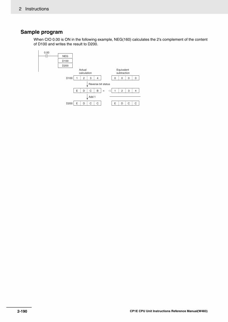
2 Instructions
Sample programWhen CIO 0.00 is ON in the following example, NEG(160) calculates the 2’s complement of the contentof D100 and writes the result to D200.
1D100 2 3 4
E D C B =
ED200 D C C
0 0 0 0
E D C C
NEG
D100
D200
0.00
1 2 3 4
Add 1
Actual calculation
Equivalent subtraction
Reverse bit status
2-190 CP1E CPU Unit Instructions Reference Manual(W483)
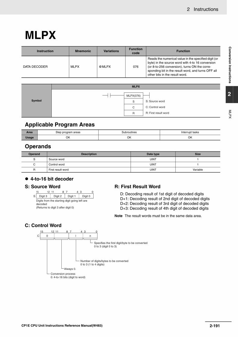
2 Instructions C
onversio
n In
structio
ns
2
MLP
X
MLPX
Applicable Program Areas
Operands
4-to-16 bit decoder
C: Control Word
Instruction Mnemonic VariationsFunction
codeFunction
DATA DECODER MLPX @MLPX 076
Reads the numerical value in the specified digit (or byte) in the source word with 4-to 16 conversion (or 8-to-256 conversion), turns ON the corre-sponding bit in the result word, and turns OFF all other bits in the result word.
Symbol
MLPX
Area Step program areas Subroutines Interrupt tasks
Usage OK OK OK
Operand Description Data type Size
S Source word UINT 1
C Control word UINT 1
R First result word UINT Variable
S: Source Word R: First Result WordD: Decoding result of 1st digit of decoded digitsD+1: Decoding result of 2nd digit of decoded digitsD+2: Decoding result of 3rd digit of decoded digitsD+3: Decoding result of 4th digit of decoded digits
Note The result words must be in the same data area.
S: Source word
C: Control word
R: First result word
MLPX(076)
S
C
R
S Digit 3 Digit 2
8111215
Digit 1 Digit 0
0347
Digits from the starting digit going left are decoded(Returns to digit 3 after digit 0)
C 0
8111215
l n
0347
Conversion process0: 4-to-16 bits (digit to word)
Always 0.
Number of digits/bytes to be converted0 to 3 (1 to 4 digits)
Specifies the first digit/byte to be converted0 to 3 (digit 0 to 3)
2-191CP1E CPU Unit Instructions Reference Manual(W483)

2 Instructions
8-to-256 bit conversion
C: Control Word
Operand Specifications
Flags
FunctionMLPX(076) can perform 4-to-16 bit or 8-to-256 bit conversions. Set the leftmost digit of C to 0 to specify4-to-16 bit conversion and set it to 1 to specify 8-to-256 bit conversion.
S: Source Word R: First Result WordD+15 to D: Decoding result of 1st digit of decoded digitsD+31 to D+16:
Decoding result of 2nd digit of decoded digits
Note The result words must be in the same data area.
Area Word addresses Indirect DM addresses
Constants CF Pulse bits TR bitsCIO WR HR AR T C DM @DM *DM
S
OK OK OK OK OK OK OK OK OK
---
--- --- ---C OK
R ---
Name Label Operation
Error Flag P_ER • ON if C is not within the specified ranges.
• OFF in all other cases.
4-to-16 bit ConversionWhen the leftmost digit of C is 0,MLPX(076) takes the value of the speci-fied digit in S (0 to F) and turns ON thecorresponding bit in the result word. Allother bits in the result word will be turnedOFF. Up to four digits can be converted.
S
815Digit 1 Digit 0
07
Digits from the starting digit going left are decoded(Returns to digit 0 after digit 1)
C 1
8111215
l n
0347
Conversion process1: 8-to-256 bits (byte to 16-word range)
Always 0.
Number of digits/bytes to be converted0 or 1 (1 or 2 bytes)
Specifies the first digit/byte to be converted0 or 1 (byte 0 or 1)
Sn
l
11
mp 015
C 0 l n
p m
RR+1
4-to-16 bit decoding (Bit m of R is turned ON.)
n=2 (Start with third digit.)
R=1 (Convert 2 digits.)
2-192 CP1E CPU Unit Instructions Reference Manual(W483)
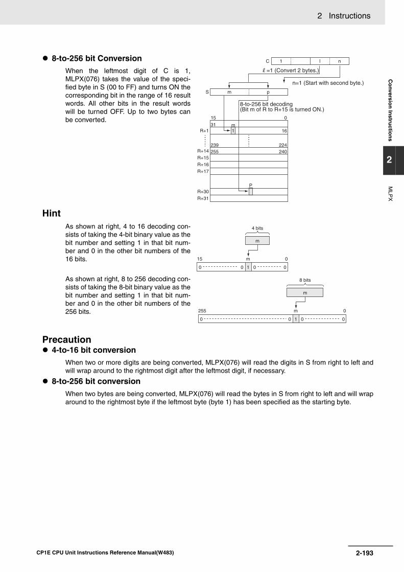
2 Instructions C
onversio
n In
structio
ns
2
MLP
X
Hint
Precaution 4-to-16 bit conversion
When two or more digits are being converted, MLPX(076) will read the digits in S from right to left andwill wrap around to the rightmost digit after the leftmost digit, if necessary.
8-to-256 bit conversionWhen two bytes are being converted, MLPX(076) will read the bytes in S from right to left and will wraparound to the rightmost byte if the leftmost byte (byte 1) has been specified as the starting byte.
8-to-256 bit ConversionWhen the leftmost digit of C is 1,MLPX(076) takes the value of the speci-fied byte in S (00 to FF) and turns ON thecorresponding bit in the range of 16 resultwords. All other bits in the result wordswill be turned OFF. Up to two bytes canbe converted.
As shown at right, 4 to 16 decoding con-sists of taking the 4-bit binary value as thebit number and setting 1 in that bit num-ber and 0 in the other bit numbers of the16 bits.
As shown at right, 8 to 256 decoding con-sists of taking the 8-bit binary value as thebit number and setting 1 in that bit num-ber and 0 in the other bit numbers of the256 bits.
S
R+1
R+14R+15R+16R+17
R+30R+31
P
1m
015
1631
224239240255
C 1 l n
pm
8-to-256 bit decoding(Bit m of R to R+15 is turned ON.)
R=1 (Convert 2 bytes.)
n=1 (Start with second byte.)
15 0m
0 0 1
m
0 0
4 bits
255 0m
0 0 1
m
0 0
8 bits
2-193CP1E CPU Unit Instructions Reference Manual(W483)

2 Instructions
Sample program 4-to-16 bit Conversion
When CIO 0.00 is ON in the following example, MLPX(076) will convert 3 digits in S beginning with digit1 (the second digit), as indicated by C (#0021). The corresponding bits in D100, D101, and D102 will beturned ON.
8-to-256 bit ConversionWhen CIO 0.00 is ON in the following example, MLPX(076) will convert the 2 bytes in S beginning withbyte 1 (the leftmost byte), as indicated by C (#1011). The corresponding bits in D100 to D115 and D116to D131 will be turned ON.
1
1
1
MLPX
100
#0021
D100
0.00
S
C
R
012345678915 14 13 12 11
0347815 12 11
10
0123
6AF
1200C: #
S: 100Digits
R: D100
D101
D102
Bits 0 to 3: Starting digit (Digit 1)Bits 4 to 7: Number of digits (3 digits)
Digit 1 contains 6, so bit 6 is turned ON.
Digit 2 contains A, so bit 10 is turned ON.
Digit 3 contains F, so bit 15 is turned ON.
Byte 1 contains 2D, so bit 13 (D) of R+2 is turned ON.
Byte 0 contains 1A, so bit 10 (A) of R+1 is turned ON.
Bits 0 to 3: Starting byte (Byte 1)
Bits 4 to 7: Number of bytes (2 bytes)
MLPX
100
#1011
D100
0.00
S
C
R
1
R: D100
D101
D102
D103
D115
D116
D117
D118
D131
01234567891514131211
0347815 1211
10
S: 100
Byte 0Byte 1
A1D2
C: # 1101
1
2-194 CP1E CPU Unit Instructions Reference Manual(W483)
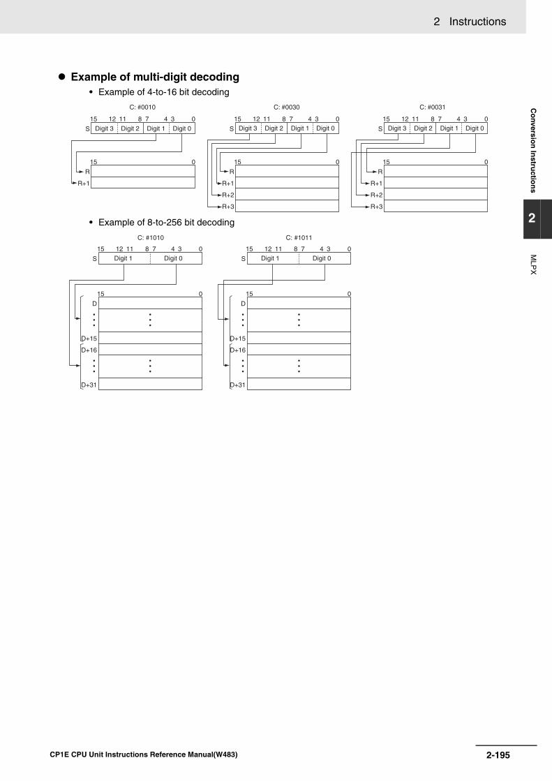
2 Instructions C
onversio
n In
structio
ns
2
MLP
X
Example of multi-digit decoding• Example of 4-to-16 bit decoding
• Example of 8-to-256 bit decoding
R
R+1
15 0
R
R+1
R+2
R+3
15 0
S Digit 3
8111215 0347
S
8111215 0347
15 0
S
8111215 0347
R
R+1
R+2
R+3
C: #0010 C: #0030 C: #0031
Digit 2 Digit 1 Digit 0 Digit 3 Digit 2 Digit 1 Digit 0 Digit 3 Digit 2 Digit 1 Digit 0
S
8111215 0
D
D+15
D+16
D+31
15 0
347
S
8111215 0
D
D+15
D+16
D+31
15 0
347
C: #1011C: #1010
Digit 1 Digit 0 Digit 1 Digit 0
2-195CP1E CPU Unit Instructions Reference Manual(W483)
2 Instructions
DMPX
Applicable Program Areas
Operands
16-to-4 bit conversion
C: Control Word
Instruction Mnemonic VariationsFunction
codeFunction
DATA ENCODER DMPX @DMPX 077
FInds the location of the first or last ON bit within the source word with 16-to-4 conversion (or 256-to-8 conversion), and writes that value to the spec-ified digit (or byte) in the result word.
Symbol
DMPX
Area Step program areas Subroutines Interrupt tasks
Usage OK OK OK
Operand Description Data type Size
S First source word UINT Variable
R Result word UINT 1
C Control word UINT 1
S: First Source WordS: 1st digit of digits to be encodedS+1: 2nd digit of digits to be encodedS+2: 3rd digit of digits to be encodedS+3: 4th digit of digits to be encoded
R: Result Word
Note The source words must be in the same dataarea.
DMPX(077)
S
R
C
S: First source word
R: Result word
C: Control word
R Digit 3 Digit 2
8111215
Digit 1 Digit 0
0347
The results of encoding of S to S+3 are stored from the starting digit going left (returns to digit 0 after digit 3).
C 0
8111215
l n
0347
Conversion process0: 16-to-4 bits (word to digit)
Bit to encode0: Leftmost bit (highest bit address)1: Rightmost bit (lowest bit address)
Number of digits/bytes to be converted0 to 3 (1 to 4 digits)
Specifies the first digit/byte to receive converted data.0 to 3 (digit 0 to 3)
2-196 CP1E CPU Unit Instructions Reference Manual(W483)

2 Instructions C
onversio
n In
structio
ns
2
DM
PX
256-to-8 bit conversion
C: Control word
Operand Specifications
Flags
FunctionDMPX(077) can perform 16-to-4 bit or 256-to-8 bit conversions. Set the leftmost digit of C to 0 to specify16-to-4 bit conversion and set it to 1 to specify 256-to-8 bit conversion.
16-to-4 bit ConversionWhen the fourth (leftmost) digit of C is 0, DMPX(077) finds the locations of the leftmost or rightmost ONbits in up to 4 source words and writes these locations to R beginning with the specified digit.
S: First Source WordS+15 to S: 1st digit of digits to be encodedS+31 to S+16: 2nd digit of digits to be encoded
R: Result Word
Note The source words must be in the samedata area.
Area Word addresses Indirect DM addresses
Constants CF Pulse bits TR bitsCIO WR HR AR T C DM @DM *DM
S,ROK OK OK OK OK OK OK OK OK
------ --- ---
C OK
Name Label Operation
Error Flag P_ER • ON if any of the source words contains 0000 hex (i.e., no bit to encode).
• ON if C is not within the specified ranges.
• OFF in all other cases.
R
815Digit 1 Digit 0
07
The results of encoding of S to S+15, S+16 toS+31 are stored from the starting digit goingleft (returns to digit 0 after digit 1).
C 1
Specifies the first digit/byte to receive converted data.0 or 1 (byte 0 or 1)
Number of digits/bytes to be converted0 or 1 (1 or 2bytes)
8111215
l n
0347
Bit to encode0: Leftmost bit (highest bit address)1: Rightmost bit (lowest bit address)
Conversion process1: 256-to-8 bits (16-word range to byte)
R
m
C
Leftmost bit
n=2 (Start with digit 2.)
R=1 (Convert 2 words.)
FInds leftmost bit(Highest bit address)
16-to-4 bit decoding(Location of leftmost bit (m) is written to R.)
n
0 0 l n
p m
S+1S 1
1
p 015
2-197CP1E CPU Unit Instructions Reference Manual(W483)
2 Instructions
256-to-8 bit ConversionWhen the fourth (leftmost) digit of C is 1, DMPX(077) finds the locations of the leftmost (highest bitaddress) or rightmost (lowest bit address) ON bits in one or two 16-word ranges of source words. Thelocations of these bits are written to R beginning with the specified byte.
Hint
Precaution 16-to-4 bit conversion
When two or more digits are being converted, DMPX(077) will write the values to the digits in R fromright to left and will wrap around to the rightmost digit after the leftmost digit, if necessary.
256-to-8 bit conversionWhen two bytes are being converted, DMPX(077) will write the values to the bytes in R from right to leftand will wrap around to the rightmost byte if the leftmost byte (byte 1) has been specified as the startingbyte.
As shown at right, 16 to 4 encoding con-sists of converting the bit number (m) ofthe leftmost or rightmost bit that has 1 setamong the 16 bits to a 4-bit binary value.
As shown at right, 256 to 8 encoding con-sists of converting the bit number (m) ofthe leftmost or rightmost bit that has 1 setamong the 256 bits to an 8-bit binaryvalue.
R
C
Leftmost bit
Rightmost bit
R=0 (Convert one 16-word range.)
Finds leftmost bit(Highest bit address)
256-to-8 bit decoding (The location of the leftmost bit in the 16-word range (m) is written to R.)
n=1 (Start with byte 1.)
0 I/0 l n
m
S+1
S+14S+15
S
1m
015
1631
224239240255
15 0m
0 0 1
m
0 0
4 bits
Rightmost ON bitLeftmost ON bit
255 0m
0 0 1
m
0 0
8 bits
Rightmost ON bit Leftmost ON bit
2-198 CP1E CPU Unit Instructions Reference Manual(W483)

2 Instructions C
onversio
n In
structio
ns
2
DM
PX
Sample program 16-to-4 bit Conversion
When CIO 0.00 is ON in the following example, DMPX(077) will find the leftmost ON bits in CIO 100,CIO 101, and CIO 102 and write those locations to 3 digits in R beginning with digit 1 (the second digit),as indicated by C (#0021).
Example of multi-digit decoding• Example of 16-to-4 bit decoding
C: #
R: D100
S
R
C
Digits
DMPX(077) finds the leftmost ON bits.
Starting digit (Digit 1)
0.00
0347815 12 11
0347815 12 11
1200
0123
5A2
1
1
1
012345678915 14 13 12 11 10
DMPX
100
D100
#0021
S: 100
101
102
C: #0032
C: #0011 C: #0030 C: #0013
R
R
R
RDigit 1Digit 3 Digit 1Digit 3
Digit 1Digit 3
Digit 1Digit 3
Digit 2 Digit 0
Digit 2 Digit 0
Digit 2 Digit 0
Digit 2 Digit 0
S
S+1
15 0
S
S+1
S+2
S+3
15 0
8111215 0347
S
S+1
15 0
8111215 0347
8111215 0347
S
S+1
S+2
S+3
15 0
8111215 0347
2-199CP1E CPU Unit Instructions Reference Manual(W483)

2 Instructions
256-to-8 bit Conversion
If the conversion data contains 0000 hex, but other data is to be encoded, separate the conversion byusing more than one DMPX(077) instructions.
DMPX(077) D0 D100 #0300
⇓
DMPX(077) D0 D100 #0000
DMPX(077) D1 D100 #0001
DMPX(077) D2 D100 #0002
DMPX(077) D3 D100 #0003
C: #1010 C: #1011
Digit 1 Digit 0 Digit 1 Digit 0S
815 0
S
S+15
S+16
S+31
15 0
7
S
815 0
S
S+15
S+16
S+31
15 0
7
2-200 CP1E CPU Unit Instructions Reference Manual(W483)

2 Instructions C
onversio
n In
structio
ns
2
AS
C
ASC
Applicable Program Areas
Operands
DI: Digit DesignatorThe digit designator specifies various parameters for the conversion, as shown in the following dia-gram.
Instruction Mnemonic VariationsFunction
codeFunction
ASCII CONVERT ASC @ASC 086Converts 4-bit hexadecimal digits in the source word into their 8-bit ASCII equivalents.
Symbol
ASC
Area Step program areas Subroutines Interrupt tasks
Usage OK OK OK
Operand Description Data type Size
S Source word UINT 1
DI Digit designator UINT 1
D First destination word UINT Variable
S: Source Word D: First Destination Word
Note The destination words must be in the samedata area.
S: Source word
DI: Digit designator
D: First destination word
ASC(086)
S
DI
D
S Digit 3 Digit 28111215
Digit 1 Digit 00347
Digits from the starting digit of conversion going left are treated as HEX data and converted to ASCII code (returns to digit 0 after digit 3)
D
D+1
D+2
815Leftmost byte Rightmost byte
07
ASCII code is stored in the left word side. The code is stored from the output starting byte of D in the order rightmost byte, leftmost byte.
Leftmost byte Rightmost byte
Leftmost byte Rightmost byte
Specifies the first digit in S to be converted (0 to 3).
Number of digits to be converted (0 to 3) 0: 1 digit 1: 2 digits 2: 3 digits 3: 4 digits
First byte of D to be used.
0: Rightmost byte 1: Leftmost byte
Parity 0: None 1: Even2: Odd
Digit number: 3 2 1 0
2-201CP1E CPU Unit Instructions Reference Manual(W483)

2 Instructions
Operand Specifications
Flags
Function
Hint• The parity bit is appended to the data to enable detection of errors when the data is transmitted. By
adding this bit, the number of bits that are 1 in the data can be indicated as odd or even, and if thenumber of 1s in the received data is not similarly odd or even, it is assumed that an error hasoccurred.
Precaution• When multiple digits are specified in the number of digits to be converted (K), the digits are converted
in order from the starting conversion digit going left (returns to digit 0 after digit 3), and the conversionresults are stored in order from the output position of D going to the left word side (in units of 8 bits).
• Among the data in the conversion result output word, data in positions that are not to be output areheld.
• When converting multiple digits, take care that D+1 and D+2CH do not exceed the area.
Area Word addresses Indirect DM addresses
Constants CF Pulse bits TR bitsCIO WR HR AR T C DM @DM *DM
S
OK OK OK OK OK OK OK OK OK
---
--- --- ---DI OK
D ---
Name Label Operation
Error Flag P_ER • ON if the content of Di is not within the specified ranges.
• OFF in all other cases.
ASC(086) treats the contents of S as 4 hexadec-imal digits, converts the designated digit(s) of Sinto their 8-bit ASCII equivalents, and writes thisdata into the destination word(s) beginning withthe specified byte in D.A parity specification (bits 12 to 15 of K) is pos-sible in the leftmost bit of the ASCII code data,and this can be converted to an odd or even par-ity bit (the number of bits that are 1 of the eightbits is adjusted to odd or even).
D
0 1/0 n m
33
Sm321
31 32
HEX
ASCII
Di
Right (0)Left (1)
Number of digits (n+1)
First digit to convert
2-202 CP1E CPU Unit Instructions Reference Manual(W483)

2 Instructions C
onversio
n In
structio
ns
2
AS
C
Sample programWhen CIO 0.00 is ON in the following example, ASC(086) converts three hexadecimal digits in D100(beginning with digit 1) into their ASCII equivalents and writes this data to D200 and D201 beginningwith the leftmost byte in D200. In this case, a digit designator of #0121 specifies no parity, the startingbyte (when writing) = leftmost byte, the number of digits to read = 3, and the starting digit (when read-ing) = digit 1.
Example of ASCII code conversion
* Parity bit - changes according to the parity specification.
Content of conversion data digits Conversion output data
Value Bit content Code (MSB) bit content (LSB)
0 0 0 0 0 #30 * 0 1 1 0 0 0 0
1 0 0 0 1 #31 * 0 1 1 0 0 0 1
2 0 0 1 0 #32 * 0 1 1 0 0 1 0
3 0 0 1 1 #33 * 0 1 1 0 0 1 1
4 0 1 0 0 #34 * 0 1 1 0 1 0 0
5 0 1 0 1 #35 * 0 1 1 0 1 0 1
6 0 1 1 0 #36 * 0 1 1 0 1 1 0
7 0 1 1 1 #37 * 0 1 1 0 1 1 1
8 1 0 0 0 #38 * 0 1 1 1 0 0 0
9 1 0 0 1 #39 * 0 1 1 1 0 0 1
A 1 0 1 0 #41 * 1 0 0 0 0 0 1
B 1 0 1 1 #42 * 1 0 0 0 0 1 0
C 1 1 0 0 #43 * 1 0 0 0 0 1 1
D 1 1 0 1 #44 * 1 0 0 0 1 0 0
E 1 1 1 0 #45 * 1 0 0 0 1 0 1
F 1 1 1 1 #46 * 1 0 0 0 1 1 0
D: D200
D201
ASC
D100
#0121
D200
0.00
S
Di
D
0347815 12 11
0347815 12 11
1210
0123
321
07815
33
3231
S: D100
Di: #
Number of digits
Digits
HEX
ASCII
Starting digit
Starting byte (leftmost byte)
2-203CP1E CPU Unit Instructions Reference Manual(W483)

2 Instructions
ParityIt is possible to specify the parity of the ASCII data for use in error control during data transmissions.The leftmost bit of each ASCII character will be automatically adjusted for even, odd, or no parity.
• When no parity (0) is designated, the leftmost bit will always be zero. When even parity (1) is desig-nated, the leftmost bit will be adjusted so that the total number of ON bits is even. When odd parity (2)is designated, the leftmost bit of each ASCII character will be adjusted so that there is an odd numberof ON bits. The status of the parity bit does not affect the meaning of the ASCII code.
• Examples of even parity:When adjusted for even parity, ASCII “31” (00110001) will be “B1” (10110001: parity bit turned ON tocreate an even number of ON bits); ASCII “36” (00110110) will be “36” (00110110: parity bit remainsOFF because the number of ON bits is already even).
• Examples of odd parity:When adjusted for odd parity, ASCII “36” (00110110) will be “B6” (10110110: parity bit turned ON tocreate an odd number of ON bits); ASCII “46” (01000110) will be “46” (01000110: parity bit remainsOFF because the number of ON bits is already odd).
Examples of DiDi: #0011 Di: #0112 Di: #0030
Di: #0130
Digit 3 Digit 2 Digit 1 Digit 0
Leftmost Rightmost
Digit 3 Digit 2 Digit 1 Digit 0 Digit 3 Digit 2 Digit 1 Digit 0
Leftmost
Rightmost
Leftmost Rightmost
Leftmost Rightmost
Digit 3 Digit 2 Digit 1 Digit 0
Leftmost
Rightmost
Rightmost
Leftmost
D D
D+1
S
8111215 0347
S
8111215 0347
D
D+1
S
8111215 0347
815 07 815 07 815 07
D
D+1
D+2
S
8111215 0347
815 07
2-204 CP1E CPU Unit Instructions Reference Manual(W483)

2 Instructions C
onversio
n In
structio
ns
2
HE
X
HEX
Applicable Program Areas
Operands
DI: Digit DesignatorThe digit designator specifies various parameters for the conversion, as shown in the following dia-gram.
Instruction Mnemonic VariationsFunction
codeFunction
ASCII TO HEX HEX @HEX 162Converts up to 4 bytes of ASCII data in the source word to their hexadecimal equivalents and writes these digits in the specified destination word.
Symbol
HEX
Area Step program areas Subroutines Interrupt tasks
Usage OK OK OK
Operand Description Data type Size
S First source word UINT Variable
DI Digit designator UINT 1
D Destination word UINT 1
S: First Source Word D: Destination Word
S: First source word
DI: Digit designator
D: Destination word
HEX(162)
S
DI
D
S
815Leftmost byte Rightmost byte
07
The conversion start byte and bytes to the left are treated as ASCII code and converted to hex (returns to the rightmost byte after the leftmost byte.
D Digit 3 Digit 28111215
Digit 1 Digit 00347
The results of conversion to hex are stored from the starting digit going left (returns to digit 0 after digit 3)
Digit number: 3 2 1 0
Specifies the first digit in D to receive converted data (0 to 3).
Number of bytes to be converted (0 to 3) 0: 1 digit 1: 2 digits 2: 3 digits 3: 4 digits
0: Rightmost byte1: Leftmost byte
Parity 0: None 1: Even 2: Odd
First byte of S to be converted.
2-205CP1E CPU Unit Instructions Reference Manual(W483)
2 Instructions
Operand Specifications
Flags
Function
Hint• The parity bit is appended to the data to enable detection of errors when the data is transmitted. By
adding this bit, the number of bits that are 1 in the data can be indicated as odd or even, and if thenumber of 1s in the received data is not similarly odd or even, it is assumed that an error hasoccurred.
Precaution• When multiple digits are specified in the number of digits to be converted (C), the digits are converted
in order from the starting conversion position (C) of S going to the left word side, and the conversionresults are stored in order from the output starting bit (C) of D going to the left (returns to digit 0 afterdigit 3).
• Among the data in the conversion result output word, data of bits that are not to be output are held(kept the same as before).
• The following table shows ASCII data which can be contained in the source word(s) (excluding paritybits) and corresponding hexadecimal digits.
Area Word addresses Indirect DM addresses
Constants CF Pulse bits TR bitsCIO WR HR AR T C DM @DM *DM
S
OK OK OK OK OK OK OK OK OK
---
--- --- ---DI OK
D ---
Name Label Operation
Error Flag P_ER • ON if there is a parity error in the ASCII data.
• ON if the ASCII data in the source words is not equivalent to hexadecimal digits
• ON if the content of Di is not within the specified ranges.
• OFF in all other cases.
HEX(162) treats the contents of the sourceword(s) as ASCII data representing hexa-decimal digits (0 to 9 and A to F), convertsthe specified number of bytes to hexadeci-mal, and writes the hexadecimal data to thedestination word beginning at the specifieddigit.When converting data, the leftmost bit ofthe ASCII code data can be treated as anodd or even parity bit according to the parityspecification.
ASCII data (2 hexadecimal digits) Hexadecimal digits
30 to 39 0 to 9
41 to 46 A to F
Di 0 0/1 n m
Dm234
n+1
ASCII
HEX
SS+1
33 3234
Number of digits (n+1)
Right (0)Left (1)
First digit to write
First byte to convert
2-206 CP1E CPU Unit Instructions Reference Manual(W483)

2 Instructions C
onversio
n In
structio
ns
2
HE
X
Sample programWhen CIO 0.00 is ON in the following example, HEX(162) converts the ASCII data in D100 and D101according to the settings of the digit designator. (Di=#0121 specifies no parity, the starting byte (whenreading) = leftmost byte, the number of bytes to read = 3, and the starting digit (when writing) = digit 1.)
HEX(162) converts three bytes of ASCII data (3 characters) beginning with the leftmost byte of D100into their hexadecimal equivalents and writes this data to D200 beginning with digit 1.
ParityIt is possible to specify the parity of the ASCII data for use in error control during data transmissions.The leftmost bit in each byte is the parity bit. With no parity the parity bit should always be zero, witheven parity the status of the parity bit should result in an even number of ON bits, and with odd paritythe status of the parity bit should result in an odd number of ON bits.
The following table shows the operation of HEX(162) for each parity setting.
Parity setting(leftmost digit of Di)
Operation of HEX(162)
No parity (0) HEX(162) will be executed only when the parity bit in each byte is 0. An error will occur if a parity bit is non-zero.
Even parity (1) HEX(162) will be executed only when there is an even number of ON bits in each byte. An error will occur if a byte has an odd number of ON bits.
Odd parity (2) HEX(162) will be executed only when there is an odd number of ON bits in each byte. An error will occur if a byte has an even number of ON bits.
HEX
D100
#0121
D200
0.00
S
Di
D
0347815 12 11
0347815 12 11
Di:# 1210
Di:D200
0123
345
07815
S:D100
D101
33
3435
Number of digits
3 digits
Starting digit (digit 1)
Starting byte (leftmost byte)
2-207CP1E CPU Unit Instructions Reference Manual(W483)
2 Instructions
Output example
* Parity bit - changes according to the parity specification.
When CIO 0.00 is ON in the following example, HEX(162) converts the ASCII data in D10 beginningwith the rightmost byte and writes the hexadecimal equivalents in D300 beginning with digit 1.
The digit designator setting of #1011 specifies even parity, the starting byte (when reading) = rightmostbyte, the number of bytes to read = 2, and the starting digit (when writing) = digit 1.)
Conversion data Output result (hex data)
ASCII code
(MSB) bit content (LSB) Value Bit content
#30 * 0 1 1 0 0 0 0 0 0 0 0 0
#31 * 0 1 1 0 0 0 1 1 0 0 0 1
#32 * 0 1 1 0 0 1 0 2 0 0 1 0
#33 * 0 1 1 0 0 1 1 3 0 0 1 1
#34 * 0 1 1 0 1 0 0 4 0 1 0 0
#35 * 0 1 1 0 1 0 1 5 0 1 0 1
#36 * 0 1 1 0 1 1 0 6 0 1 1 0
#37 * 0 1 1 0 1 1 1 7 0 1 1 1
#38 * 0 1 1 1 0 0 0 8 1 0 0 0
#39 * 0 1 1 1 0 0 1 9 1 0 0 1
#41 * 1 0 0 0 0 0 1 A 1 0 1 0
#42 * 1 0 0 0 0 1 0 B 1 0 1 1
#43 * 1 0 0 0 0 1 1 C 1 1 0 0
#44 * 1 0 0 0 1 0 0 D 1 1 0 1
#45 * 1 0 0 0 1 0 1 E 1 1 1 0
#46 * 1 0 0 0 1 1 0 F 1 1 1 1
Number of bytes (2 bytes)
Starting digit (digit 1)
Parity bits: Result in even parity
Not changed
Not changed
Conversion
Parity: Even
Starting byte: rightmost
Starting digit in D: Digit 1Number of bytes: 2Starting byte in S: Rightmost
HEX
D10
#1011
D300
0.00
0347815 12 11
1101
D: D300 8C
015
015
S: D100 1 1 0 0 0 0 1 1 1 0 1 1 1 0 0 0
3843
2-208 CP1E CPU Unit Instructions Reference Manual(W483)

2 Instructions C
onversio
n In
structio
ns
2
HE
X
Example of converting multiple bytes of ASCII code to hexDi: #0112 Di: #0030 Di: #0131
Digit 3 Digit 2 Digit 1 Digit 0
Leftmost
Rightmost
Digit 3 Digit 2 Digit 1 Digit 0
Digit 3 Digit 2 Digit 1 Digit 0
Leftmost Rightmost
Leftmost Rightmost
Leftmost
Rightmost
Leftmost Rightmost
S
S+1
D
8111215 0347
D
8111215 0347
S
S+1
S+2
F
8111215 0347
8 815 0 15 077 815 07
S
S+1
2-209CP1E CPU Unit Instructions Reference Manual(W483)

2 Instructions
Logic Instructions
ANDW/ANDL
Applicable Program Areas
Operands
Operand Specifications
Flags
Instruction Mnemonic VariationsFunction
codeFunction
LOGICAL AND ANDW @ANDW 034Takes the logical AND of corresponding bits in sin-gle words of word data and/or constants.
DOUBLE LOGICAL AND ANDL @ANDL 610Takes the logical AND of corresponding bits in double words of word data and/or constants.
Symbol
ANDW ANDL
Area Step program areas Subroutines Interrupt tasks
Usage OK OK OK
Operand Description Data type Size
ANDW ANDL ANDW ANDL
I1 Input 1 WORD DWORD 1 2
I2 Input 2 WORD DWORD 1 2
R Result word WORD DWORD 1 2
Area Word addresses Indirect DM addresses
Constants CF Pulse bits TR bitsCIO WR HR AR T C DM @DM *DM
I1, I2OK OK OK OK OK OK OK OK OK
OK--- --- ---
R ---
Name Label Operation
Error Flag P_ER OFF
Equals Flag P_EQ • ON when the result is 0.
• OFF in all other cases.
Negative Flag P_N • ON when the leftmost bit of R is 1.
• OFF in all other cases.
I1: Input 1
I2: Input 2
R: Result word
ANDW(034)
I1
I2
R
I1: Input 1
I2: Input 2
R: Result word
ANDL(610)
I1
I2
R
2-210 CP1E CPU Unit Instructions Reference Manual(W483)

2 Instructions L
og
ic Instru
ction
s
2
AN
DW
/AN
DL
Function
Sample programWhen the execution condition CIO 0.00 is ON, the logical AND is taken of corresponding bits in CIO 11,CIO 10 and CIO 21, CIO 20 and the results will be output to corresponding bits in D201 and D200.
ANDWANDW(034) takes the logical AND of data spec-ified in I1 and I2 and outputs the result to R.
ANDLANDL(610) takes the logical AND of data speci-fied in I1, I1+1 and I2, I2+1 and outputs the resultto R, R+1.
I1, I2 → R
I1 I2 R
1 1 1
1 0 0
0 1 0
0 0 0
(I1, I1+1) • (I2, I2+1) → (R, R+1)
I1, I1+1 I2, I2+1 R, R+1
1 1 1
1 0 0
0 1 0
0 0 0
10.00 0
10.01 1
10.02 0
10.03 1
10.04 0
11.13 1
11.14 1
11.15 0
ANDL
10
20
D200
0.00S1: 10CH
S1+1: 11CH
20.00 1
20.01 1
20.02 0
20.03 0
20.04 1
21.13 1
21.14 0
21.15 0
S2: 20CHS2+1: 21CH
00 0
01 1
02 0
03 0
04 0
13 1
14 0
15 0
D: D200D+1: D201
Note The vertical arrow indicates logical AND.
2-211CP1E CPU Unit Instructions Reference Manual(W483)

2 Instructions
ORW/ORWL
Applicable Program Areas
Operands
Operand Specifications
Flags
Instruction Mnemonic VariationsFunction
codeFunction
LOGICAL OR ORW @ORW 035Takes the logical OR of corresponding bits in sin-gle words of word data and/or constants.
DOUBLE LOGICAL OR ORWL @ORWL 611Takes the logical OR of corresponding bits in dou-ble words of word data and/or constants.
Symbol
ORW ORWL
Area Step program areas Subroutines Interrupt tasks
Usage OK OK OK
Operand Description Data type Size
ORW ORWL ORW ORWL
I1 Input 1 WORD DWORD 1 2
I2 Input 2 WORD DWORD 1 2
R Result word WORD DWORD 1 2
Area Word addresses Indirect DM addresses
Constants CF Pulse bits TR bitsCIO WR HR AR T C DM @DM *DM
I1, I2OK OK OK OK OK OK OK OK OK
OK--- --- ---
R ---
Name Label Operation
Error Flag P_ER OFF
Equals Flag P_EQ • ON when the result is 0.
• OFF in all other cases.
Negative Flag P_N • ON when the leftmost bit of R is 1.
• OFF in all other cases.
I1: Input 1
I2: Input 2
R: Result word
ORW(035)
I1
I2
R
I1: Input 1
I2: Input 2
R: Result word
ORWL(611)
I1
I2
R
2-212 CP1E CPU Unit Instructions Reference Manual(W483)

2 Instructions L
og
ic Instru
ction
s
2
OR
W/O
RW
L
Function
Sample programWhen the execution condition CIO 0.00 is ON, the logical OR is taken of corresponding bits in CIO 21,CIO 20 and CIO 31, CIO 30 and the results will be output to corresponding bits in D501 and D500.
ORWORW(035) takes the logical OR of data speci-fied in I1 and I2 and outputs the result to R.
ORWLORWL(611) takes the logical OR of dataspecified in I1 and I2 as double-word data andoutputs the result to R, R+1.
I1, I2 → R
I1 I2 R
1 1 1
1 0 1
0 1 1
0 0 0
(I1, I1+1) + (I2, I2+1) → (R, R+1)
I1, I1+1 I2, I2+1 R, R+1
1 1 1
1 0 1
0 1 1
0 0 0
20.00
20.01
20.02
20.03
20.15
21.00
21.15
1
1
0
0
1
1
0
1
1
1
0
1
1
1
1
0
1
0
1
0
1
ORWL
20
30
D500
0.00S1: 20CH
S1+1: 21CH
30.00
30.01
30.02
30.03
30.15
31.00
31.15
S2: 30CHS2+1: 31CH
00
01
02
03
15
00
15
D: D500D+1: D501
D500
D501
Note The vertical arrow indicates logical OR.
2-213CP1E CPU Unit Instructions Reference Manual(W483)
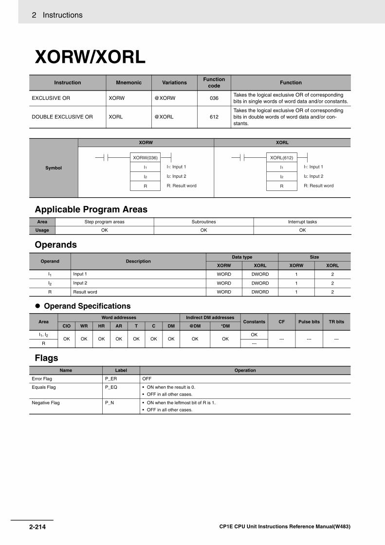
2 Instructions
XORW/XORL
Applicable Program Areas
Operands
Operand Specifications
Flags
Instruction Mnemonic VariationsFunction
codeFunction
EXCLUSIVE OR XORW @XORW 036Takes the logical exclusive OR of corresponding bits in single words of word data and/or constants.
DOUBLE EXCLUSIVE OR XORL @XORL 612Takes the logical exclusive OR of corresponding bits in double words of word data and/or con-stants.
Symbol
XORW XORL
Area Step program areas Subroutines Interrupt tasks
Usage OK OK OK
Operand Description Data type Size
XORW XORL XORW XORL
I1 Input 1 WORD DWORD 1 2
I2 Input 2 WORD DWORD 1 2
R Result word WORD DWORD 1 2
Area Word addresses Indirect DM addresses
Constants CF Pulse bits TR bitsCIO WR HR AR T C DM @DM *DM
I1, I2OK OK OK OK OK OK OK OK OK
OK--- --- ---
R ---
Name Label Operation
Error Flag P_ER OFF
Equals Flag P_EQ • ON when the result is 0.
• OFF in all other cases.
Negative Flag P_N • ON when the leftmost bit of R is 1.
• OFF in all other cases.
I1: Input 1
I2: Input 2
R: Result word
XORW(036)
I1
I2
R
I1: Input 1
I2: Input 2
R: Result word
XORL(612)
I1
I2
R
2-214 CP1E CPU Unit Instructions Reference Manual(W483)

2 Instructions L
og
ic Instru
ction
s
2
XO
RW
/XO
RL
Function
Sample programWhen the execution condition CIO 0.00 is ON, the logical exclusive OR is taken of corresponding bits inCIO 151, CIO 150 and D1001, D1000 and the results will be output to corresponding bits in D1201 andD1200.
XORWXORW(036) takes the logical exclusive OR ofdata specified in I1 and I2 and outputs theresult to R.
XORLXORL(612) takes the logical exclusive OR ofdata specified in I1 and I2 as double-word dataand outputs the result to R, R+1.
I1 • I2 + I1 • I2 → R
I1 I2 R
1 1 0
1 0 1
0 1 1
0 0 0
(I1, I1+1) • (I2, I2+1) + (I1, I1+1) • (I2, I2+1) → (R, R+1)
I1, I1+1 I2, I2+1 R, R+1
1 1 0
1 0 1
0 1 1
0 0 0
150.00
150.01
150.02
150.03
150.15
151.00
151.15
00
01
02
03
15
00
15
1
1
0
0
1
1
0
1
0
1
0
1
0
1
00
01
02
03
15
00
15
0
1
1
0
0
1
1
XORL
150
D1000
D1200
0.00S1: 150CH
S1+1: 151CHS2: D1000
S2+1: D1001D: D1200
D+1: D1201
D1200
D1201
D1000
D1001
Note The symbol indicates exclusive logical OR.
2-215CP1E CPU Unit Instructions Reference Manual(W483)
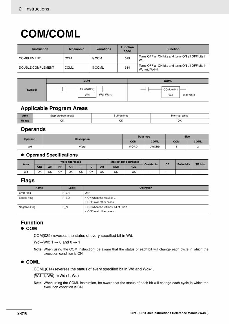
2 Instructions
COM/COML
Applicable Program Areas
Operands
Operand Specifications
Flags
Function COM
COM(029) reverses the status of every specified bit in Wd.
Wd→Wd: 1 → 0 and 0 → 1
Note When using the COM instruction, be aware that the status of each bit will change each cycle in which theexecution condition is ON.
COMLCOML(614) reverses the status of every specified bit in Wd and Wd+1.
(Wd+1, Wd)→(Wd+1, Wd)
Note When using the COML instruction, be aware that the status of each bit will change each cycle in which theexecution condition is ON.
Instruction Mnemonic VariationsFunction
codeFunction
COMPLEMENT COM @COM 029Turns OFF all ON bits and turns ON all OFF bits in Wd.
DOUBLE COMPLEMENT COML @COML 614Turns OFF all ON bits and turns ON all OFF bits in Wd and Wd+1.
Symbol
COM COML
Area Step program areas Subroutines Interrupt tasks
Usage OK OK OK
Operand Description Data type Size
COM COML COM COML
Wd Word WORD DWORD 1 2
Area Word addresses Indirect DM addresses
Constants CF Pulse bits TR bitsCIO WR HR AR T C DM @DM *DM
Wd OK OK OK OK OK OK OK OK OK --- --- --- ---
Name Label Operation
Error Flag P_ER OFF
Equals Flag P_EQ • ON when the result is 0.
• OFF in all other cases.
Negative Flag P_N • ON when the leftmost bit of R is 1.
• OFF in all other cases.
COM(029)
Wd Wd: Word Wd: Word
COML(614)
Wd
2-216 CP1E CPU Unit Instructions Reference Manual(W483)
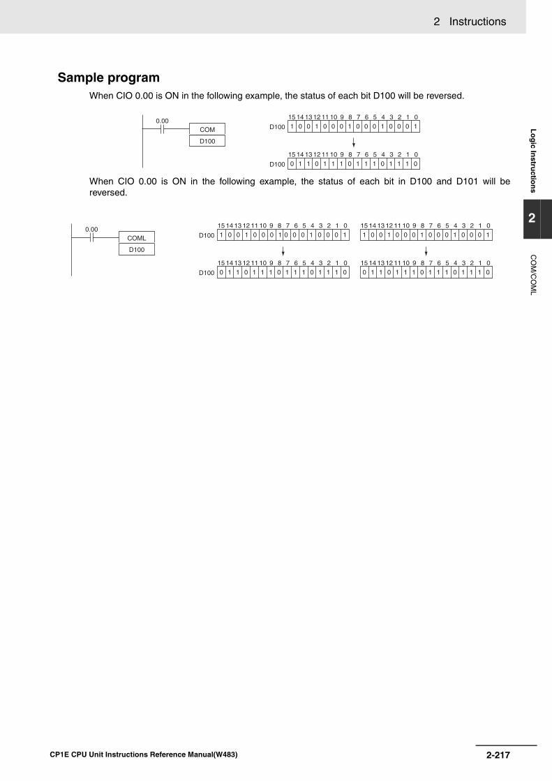
2 Instructions L
og
ic Instru
ction
s
2
CO
M/C
OM
L
Sample programWhen CIO 0.00 is ON in the following example, the status of each bit D100 will be reversed.
When CIO 0.00 is ON in the following example, the status of each bit in D100 and D101 will bereversed.
D100 1 0 0 1 0 0 0 1 0 0 0 1 0 0 0 1012345678915 14 13 12 11 10
D100 0 1 1 0 1 1 1 0 1 1 1 0 1 1 1 0012345678915 14 13 12 11 10
COM
D100
0.00
COML
D100
0.00D100 1 0 0 1 0 0 0 1 0 0 0 1 0 0 0 1
012345678915 14 13 12 11 10
D100 0 1 1 0 1 1 1 0 1 1 1 0 1 1 1 0012345678915 14 13 12 11 10
1 0 0 1 0 0 0 1 0 0 0 1 0 0 0 1012345678915 14 13 12 11 10
0 1 1 0 1 1 1 0 1 1 1 0 1 1 1 0012345678915 14 13 12 11 10
2-217CP1E CPU Unit Instructions Reference Manual(W483)
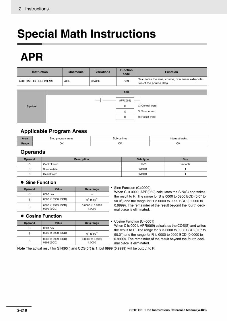
2 Instructions
Special Math Instructions
APR
Applicable Program Areas
Operands
Sine Function
Cosine Function
Instruction Mnemonic VariationsFunction
codeFunction
ARITHMETIC PROCESS APR @APR 069Calculates the sine, cosine, or a linear extrapola-tion of the source data.
Symbol
APR
Area Step program areas Subroutines Interrupt tasks
Usage OK OK OK
Operand Description Data type Size
C Control word UINT Variable
S Source data WORD 1
R Result word WORD 1
• Sine Function (C=0000)When C is 0000, APR(069) calculates the SIN(S) and writes the result to R. The range for S is 0000 to 0900 BCD (0.0° to 90.0°) and the range for R is 0000 to 9999 BCD (0.0000 to 0.9999). The remainder of the result beyond the fourth deci-mal place is eliminated.
• Cosine Function (C=0001)When C is 0001, APR(069) calculates the COS(S) and writes the result to R. The range for S is 0000 to 0900 BCD (0.0° to 90.0°) and the range for R is 0000 to 9999 BCD (0.0000 to 0.9999). The remainder of the result beyond the fourth deci-mal place is eliminated.
Note The actual result for SIN(90°) and COS(0°) is 1, but 9999 (0.9999) will be output to R.
C: Control word
S: Source word
R: Result word
APR(069)
C
S
R
Operand Value Data range
C 0000 hex ---
S 0000 to 0900 (BCD) 0° to 90°
R0000 to 9999 (BCD)9999 (BCD)
0.0000 to 0.99991.0000
Operand Value Data range
C 0001 hex ---
S 0000 to 0900 (BCD) 0° to 90°
R0000 to 9999 (BCD)9999 (BCD)
0.0000 to 0.99991.0000
2-218 CP1E CPU Unit Instructions Reference Manual(W483)
2 Instructions S
pecial M
ath In
structio
ns
2
AP
R
Linear Extrapolation Function• Linear Extrapolation (C = Data area address)
APR(069) linear extrapolation is specified when C is a word address. The content of word C specifies the number of coordinates in a data table starting at C+2, the form of the source data, and whether data is BCD or binary.
The following 5 kinds of I/O data can be used:
• 16-bit unsigned BCD data
• 16-bit unsigned binary data
• 16-bit signed binary data
• 32-bit signed binary data
• Single-precision floating-point data
Operand Value Data range
C Data area address ---
S
16-bit unsigned BCD data 0000 to 9999
16-bit unsigned binary data
0 to 65,535
16-bit signed binary data -32,768 to 32,767
32-bit signed binary data -2,147,483,648 to 2,147,483,647
Floating-point data -∞,
-3.402823 × 1038 to
-1.175494 × 10-38,
1.175494 × 10-38 to
3.402823 × 1038,
+∞
R
16-bit unsigned BCD data 0000 to 9999
16-bit unsigned binary data
0 to 65,535
16-bit signed binary data -32,768 to 32,767
32-bit signed binary data -2,147,483,648 to 2,147,483,647
Floating-point data -∞,
-3.402823 × 1038 to
-1.175494 × 10-38,
1.175494 × 10-38 to
3.402823 × 1038,
+∞
C 0
314 13 12 11 910 8 7 6 5 4 2 115
0
0
000
Number of coordinates minus one (m-1), 00 to FF hex (1 ≤ m ≤ 256)
· Unsigned Integer Data (Binary or BCD)
Floating-point specification for S and D 0: Integer data
Signed data specification for S and D0: Unsigned binary data
Source data form0: f(x) = f(S)1: f(x) = f(Xm - S)
Output (D) data format0: Binary1: BCD
Input (S) data format0: Binary1: BCD
2-219CP1E CPU Unit Instructions Reference Manual(W483)

2 Instructions
Operand Specifications
Area Word addresses Indirect DM addresses
Constants CF Pulse bits TR bitsCIO WR HR AR T C DM @DM *DM
C,SOK OK OK OK OK OK OK OK OK
OK--- --- ---
R ---
C 0
314 13 12 11 910 8 7 6 5 4 2 115
0
0
00 10 0
Floating-point specification for S and D 0: Integer data
Data length specification for S and D (note 1)0: 16-bit signed binary data1: 32-bit signed binary data
Signed data specification for S and D1: Signed binary data
· Signed Integer Data (Binary)
Number of coordinates minus one (m-1), 00 to FF hex (1 ≤ m ≤ 256)
C 0
314 13 12 11 910 8 7 6 5 4 2 115
0
0
10 0 0 0 0
Floating-point specification for S and D 1: Single-precision floating-point data
· Single-precision Floating-point Data
Number of coordinates minus one (m-1), 00 to FF hex (1 ≤ m ≤ 256)
C+1
C+2
C+3
C+4
C+5
C+6
C+ (2m+1)
C+ (2m+2)
X0 (*1)
Y0
X1
Y1
X2
Y2
Xn
Yn
Xm
Ym
C+1
C+2
C+3
C+4
C+5
C+6
C+7
C+8
C+ (4n+1)
C+ (4n+2)
C+ (4n+3)
C+ (4n+4)
C+ (4m+1)
C+ (4m+2)
C+ (4m+3)
C+ (4m+4)
C+1
C+2
C+3
C+4
C+5
C+6
C+7
C+8
C+ (4n+1)
C+ (4n+2)
C+ (4n+3)
C+ (4n+4)
C+ (4m+1)
C+ (4m+2)
C+ (4m+3)
C+ (4m+4)
X0 (rightmost 16 bits)
X0 (leftmost 16 bits)
Y0 (rightmost 16 bits)
Y0 (leftmost 16 bits)
X1 (rightmost 16 bits)
X1 (leftmost 16 bits)
Y1 (rightmost 16 bits)
Y1 (leftmost 16 bits)
to
Xn (rightmost 16 bits)
Xn (leftmost 16 bits)
Yn (rightmost 16 bits)
Yn (leftmost 16 bits)
to
Xm (rightmost 16 bits)
Xm (leftmost 16 bits)
Ym (rightmost 16 bits)
Ym (leftmost 16 bits)
Note: The X coordinates must be in ascending order: X1 < X2 < ... < Xm. Input all values of (Xn, Yn) as binary data, regardless of the data format specified in control word C.
16-bit BCD16-bit binary (signed orunsigned) or 16-bit BCD data
32-bit signed binary data Floating-point data
to
to
to
to
Note: Write Xm (max. X value in the table) in word C+1 when the I/O data in S and D contain unsigned data (bit 11 of C = 0).
2-220 CP1E CPU Unit Instructions Reference Manual(W483)
2 Instructions S
pecial M
ath In
structio
ns
2
AP
R
Flags
Function Operation of the Linear Extrapolation Function
APR(069) processes the input data specified in S with the following equation and the line-segment data(Xn, Yn) specified in the table beginning at C+1. The result is output to the destination word(s) specifiedwith D.
1. For S < X0Converted value = Y02. For X0 ≤ S ≤ Xmax, if Xn < S < Xn+1Converted value = Yn +[Yn + 1 - Yn/Xn + 1 - Xn] × Input data S - Xn3. Xmax < SConverted value = Ymax
Up to 256 endpoints can be stored in the line-segment data table beginning at C+1.
Name Label Operation
Error Flag P_ER • ON if C is a constant greater than 0001.
• ON if C is a word address but the X coordinates are not in ascending order (X1 ≤ X2 ≤ ... ≤ Xm).
• ON if C is a word address and bits 9, 11, and 15 of C indicate BCD input, but S is not BCD.
• ON if C is a word address and bit 9 of C indicates floating-point data, but S is a one-word constant.
• ON if C is 0000 or 0001 but S is not BCD between 0000 and 0900.
• OFF in all other cases.
Equals Flag P_EQ • ON if the result is 0.
• OFF in all other cases.
Negative Flag P_N • ON if bit 15 of R is ON.
• OFF in all other cases.
Y0
X0
Y (Binary data)
Ymax
Xmax X (Binary data)
Yn
Yn+1
Xn Xn+1S
f(S)=
D
Yn+
Y (binary data)
Equation:
Calculationresult
X (binary data)
Input data
Xn+1-Xn
2-221CP1E CPU Unit Instructions Reference Manual(W483)

2 Instructions
16-bit Unsigned BCD DataThe input data and/or the output data canbe 16-bit unsigned BCD data. Also, the lin-ear extrapolation function can be set tooperate on the value specified in S directlyor on Xm-S. (Xm is the maximum value of Xin the line-segment data.)
16-bit Unsigned Binary DataThe input data and/or the output data canbe 16-bit unsigned binary data. Also, thelinear extrapolation function can be set tooperate on the value specified in S directlyor on Xm-S. (Xm is the maximum value of Xin the line-segment data.)
16-bit Signed Binary Data
32-bit Signed Binary Data
Setting name Bit in C Setting
Input data (S) format15
0: Binary
1: BCD
Output data (D) format14
0: Binary
1: BCD
Source data form13
0: Operate on S
1: Operate on Xm-S
Signed data specification for S and D
110: Unsigned data
Data length specification for S and D
10Invalid (fixed at 16 bits)
Floating-point specification 09 0: Integer data
Setting name Bit in C Setting
Input data (S) format 15 0: Binary
Output data (D) format 14 0: Binary
Source data form 13 0
Signed data specification for S and D
111: Signed data
Data length specification for S and D
100: 16-bit signed binary data
Floating-point specification 09 0: Integer data
Note If the “Data length specification for S and D” in bit 10 of C is set to 1 anda 16-bit constant is input for S, the input data will be converted to 32-bitsigned binary before the linear extrapolation calculation.
Setting name Bit in C Setting
Input data (S) format 15 0: Binary
Output data (D) format 14 0: Binary
Source data form 13 0
Signed data specification for S and D
111: Signed data
Data length specification for S and D
101: 32-bit signed binary data
Floating-point specification 09 0: Integer data
2-222 CP1E CPU Unit Instructions Reference Manual(W483)

2 Instructions S
pecial M
ath In
structio
ns
2
AP
R
Sample program Sine Function (C: #0000)
The following example shows APR(069) used to calculate the sine of 30°.
(SIN(30) = 0.5000)
Cosine Function (C: #0001)The following example shows APR(069) used to calculate the cosine of 30°.
(COS(30) = 0.8660)
Floating-point Data
Linear Extrapolation (C: Word Address)• Using 16-bit Unsigned BCD or Binary Data
APR(069) processes the input data speci-fied in S based on the control data in C andthe line-segment data specified in the tablebeginning at C+1. The result is output to D.
Note If the “Floating-point specification” in bit 09 of C is set to 1, a constantcannot be input for S.
Setting name Bit in C Setting
Input data (S) format 15 0
Output data (D) format 14 0
Source data form 13 0
Signed data specification for S and D
110
Data length specification for S and D
100
Floating-point specification 09 1: Floating-point data
S: D0 R: D100
0 ×101 ×100 ×10–1 ×10–1 ×10–2 ×10–3 ×10⁻⁴
0 3 0 0 5 0 0 0
APR
#0000
D000
D100
0.00Source data Result
Set the source data in ×10 –1 degrees.(0000 to 0900, BCD)
Result data has four significant digits, fifth and higher digits are ignored.(0000 to 9999, BCD)
Source data Result
Set the source data in ×10–1 degrees. (0000 to 0900, BCD)
Result data has four significant digits, fifth and higher digits are ignored.(0000 to 9999, BCD)
APR
#0001
D010
D200
0.00S: D10 R: D100
0 ×101 ×100 ×10–1 ×10–1 ×10–2 ×10–3 ×10⁻⁴
0 3 0 0 8 6 6 0
Ym
Y4
Y3Y1
Y2Y0
X0 X1 X2 X3 X4 XmX
Y
2-223CP1E CPU Unit Instructions Reference Manual(W483)
2 Instructions
This example shows how to construct a linear extrapolation with 12 coordinates. The block of data iscontinuous, as it must be, from D0 to D26 (C to C + (2 × 12 + 2)). The input data is taken from CIO 10,and the result is output to CIO 11.
In this case, the source word, CIO 0010, contains 0014, and f(0014) = 0726 is output to R, CIO 0011.
The linear-extrapolation calculation is shown below.
• Yn = f(Xn), Y0 = f(X0)
• Be sure that Xn-1 < Xn in all cases.
• Input all values of (Xn, Yn) as binary data.
Word Coordinate
C+1 Xm (max. X value)
C+2 Y0
C+3 X1
C+4 Y1
C+5 X2
C+6 Y2
↓ ↓
C+(2m+1) Xm (max. X value)
C+(2m+2) Ym
D0 000B Hex
D1 05F0 Hex
D2 0000 Hex
D3 0005 Hex
D4 0F00 Hex
D5 001A Hex
D6 0402 Hex
D25 05F0 Hex
D26 1F20 Hex
0 0 0 0 0 0 0 0 0 0 0 0 1 0 1 1
15 00
x=S
X12
Y0
X1
Y1
Y2
X2
X12
Y12
Bit Bit Content Coordinate
Output and input both binary
(m–1 = 11: 12 line segments)
↓ ↓ ↓
APRD01011
0.00
X
Y
$1F20
$0F00
$0726
$0402
(0,0)$0005 $0014 $001A $05F0
(x,y)
Y 0F00 0402 0F00–001A 0005–--------------------------------- 0014 0015–( )×+=
Ω 0726=
Ω 0F00 0086 000F )×(–=
Values are all hexadecimal (Hex).
2-224 CP1E CPU Unit Instructions Reference Manual(W483)
2 Instructions S
pecial M
ath In
structio
ns
2
AP
R
• Using 32-bit Signed Binary Data In this example, APR(069) is used to convert the fluid height in a tank to fluid volume based on theshape of the holding tank.
C+1
C+2
C+3
C+4
C+5
C+6
C+7
C+8
C+ (4n+1)
C+ (4n+2)
C+ (4n+3)
C+ (4n+4)
C+ (4m+1)
C+ (4m+2)
C+ (4m+3)
C+ (4m+4)
APR
C
S
R
X0Y0
Ym
Xm
RR+1
SS+1
0
0.00
X0 (rightmost 16 bits)
X0 (leftmost 16 bits)
Y0 (rightmost 16 bits)
Y0 (leftmost 16 bits)
X1 (rightmost 16 bits)
X1 (leftmost 16 bits)
Y1 (rightmost 16 bits)
Y1 (leftmost 16 bits)
toto
to
Xn (rightmost 16 bits)
Xn (leftmost 16 bits)
Yn (rightmost 16 bits)
Yn (leftmost 16 bits)
to
Xm (rightmost 16 bits)
Xm (leftmost 16 bits)
Ym (rightmost 16 bits)
Ym (leftmost 16 bits)
Variation fromstandard = X
Fluid volume= Y
Fluid height to volume conversion table(32-bit signed binary data)
Y data range:−2,147,483,648 to 2,147,483,647
Y: Fluid volume
X: Variation from standard
Linear extrapolation of table
The linear extrapolation can usesigned source data if 32-bit signedbinary data is used.
High-resolution 32-bit signed binary data
X data range: −2,147,483,648 to 2,147,483,647
2-225CP1E CPU Unit Instructions Reference Manual(W483)

2 Instructions
• Using Floating-point Data In this example, APR(069) is used to convert the fluid height in a tank to fluid volume based on theshape of the holding tank.
C+1
C+2
C+3
C+4
C+5
C+6
C+7
C+8
C+ (4n+1)
C+ (4n+2)
C+ (4n+3)
C+ (4n+4)
C+ (4m+1)
C+ (4m+2)
C+ (4m+3)
C+ (4m+4)
X0
Y0
Ym
Xm
RR+1
SS+1
0
APR
C
S
R
0.00
Fluid height = XFluid volume= Y
Fluid height to volumeconversion table(Floating-point data)
Y data range:−∞, −3.402823 × 1038 to−1.175494 × 10−38,1.175494 × 10−38 to3.402823 × 1038, or +∞
Y: Fluid volumeX: Fluid height
Linear extrapolation of table
The linear extrapolation canprovide a smooth, high-resolutioncurve floating-point data is used.
High-resolution floating point data
X0 (rightmost 16 bits)
X0 (leftmost 16 bits)
Y0 (rightmost 16 bits)
Y0 (leftmost 16 bits)
X1 (rightmost 16 bits)
X1 (leftmost 16 bits)
Y1 (rightmost 16 bits)
Y1 (leftmost 16 bits)
to
Xn (rightmost 16 bits)
Xn (leftmost 16 bits)
Yn (rightmost 16 bits)
Yn (leftmost 16 bits)
to
Xm (rightmost 16 bits)
Xm (leftmost 16 bits)
Ym (rightmost 16 bits)
Ym (leftmost 16 bits)
to
to
X data range:−∞, −3.402823 × 1038 to −1.175494 × 10−38,1.175494 × 10−38 to 3.402823 × 1038, or +∞
2-226 CP1E CPU Unit Instructions Reference Manual(W483)
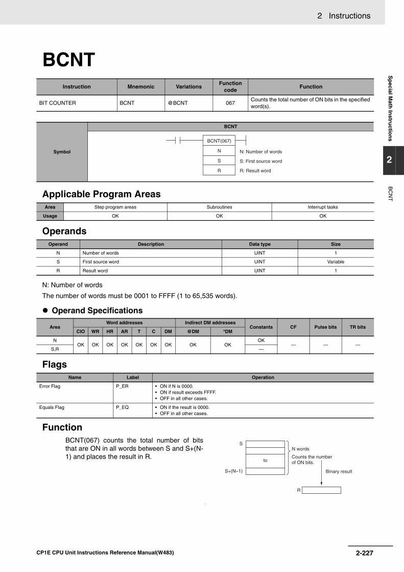
2 Instructions S
pecial M
ath In
structio
ns
2
BC
NT
BCNT
Applicable Program Areas
Operands
N: Number of words
The number of words must be 0001 to FFFF (1 to 65,535 words).
Operand Specifications
Flags
Function
T
Instruction Mnemonic VariationsFunction
codeFunction
BIT COUNTER BCNT @BCNT 067Counts the total number of ON bits in the specified word(s).
Symbol
BCNT
Area Step program areas Subroutines Interrupt tasks
Usage OK OK OK
Operand Description Data type Size
N Number of words UINT 1
S First source word UINT Variable
R Result word UINT 1
Area Word addresses Indirect DM addresses
Constants CF Pulse bits TR bitsCIO WR HR AR T C DM @DM *DM
NOK OK OK OK OK OK OK OK OK
OK--- --- ---
S,R ---
Name Label Operation
Error Flag P_ER • ON if N is 0000.• ON if result exceeds FFFF.• OFF in all other cases.
Equals Flag P_EQ • ON if the result is 0000.• OFF in all other cases.
BCNT(067) counts the total number of bitsthat are ON in all words between S and S+(N-1) and places the result in R.
N: Number of words
S: First source word
R: Result word
BCNT(067)
N
S
R
S+(N–1)
S
R
to
N words
Binary result
Counts the number of ON bits.
2-227CP1E CPU Unit Instructions Reference Manual(W483)

2 Instructions
Precautions• Some time will be required to complete BCNT(067) if a large number of words is specified. Even if an
interrupt occurs, execution of this instruction will not be interrupted and execution of the interrupt taskwill be started after execution of BCNT(067) has been completed. One BCNT(067) instruction canbe replaced with two BCNT(067) instructions to help avoid this problem.
Sample ProgramWhen CIO 0.00 is ON in the following example, BCNT(067) counts the total number of ON bits in the 10words from CIO 100 through CIO 109 and writes the result to D100.
BCNT
&1000
D1000
W0
BCNT
&500
D1000
W1
BCNT
&500
D1500
W2
+
W1
W2
W0
W1: Temporary storage
W2: Temporary storage
BCNT
&10
100
D100
0.00
0 0 2 3
100101
to
109
015
N
S
R
10 wordsCounts the number of ON bits (35).
to
R: D10023 hexadecimal (35 decimal)
2-228 CP1E CPU Unit Instructions Reference Manual(W483)
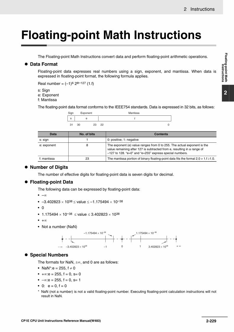
2 Instructions F
loatin
g-p
oin
t Math
Instru
ction
s
2
Floating-point Math Instructions
The Floating-point Math Instructions convert data and perform floating-point arithmetic operations.
Data FormatFloating-point data expresses real numbers using a sign, exponent, and mantissa. When data isexpressed in floating-point format, the following formula applies.
Real number = (–1)s 2e–127 (1.f)
s: Signe: Exponentf: Mantissa
The floating-point data format conforms to the IEEE754 standards. Data is expressed in 32 bits, as follows:
Number of DigitsThe number of effective digits for floating-point data is seven digits for decimal.
Floating-point DataThe following data can be expressed by floating-point data:
• –∞
• –3.402823 × 1038 ≤ value ≤ –1.175494 × 10–38
• 0
• 1.175494 × 10–38 ≤ value ≤ 3.402823 × 1038
• +∞
• Not a number (NaN)
Special NumbersThe formats for NaN, ±∞, and 0 are as follows:
• NaN*:e = 255, f ≠ 0
• +∞:e = 255, f = 0, s= 0
• –∞:e = 255, f = 0, s= 1
• 0: e = 0, f = 0* NaN (not a number) is not a valid floating-point number. Executing floating-point calculation instructions will not
result in NaN.
Data No. of bits Contents
s: sign 1 0: positive; 1: negative
e: exponent 8 The exponent (e) value ranges from 0 to 255. The actual exponent is the value remaining after 127 is subtracted from e, resulting in a range of –127 to 128. “e=0” and “e=255” express special numbers.
f: mantissa 23 The mantissa portion of binary floating-point data fits the formal 2.0 > 1.f ≥1.0.
es f
31 30 23 22 0
Sign Exponent Mantissa
–1.175494 × 10–38 1.175494 × 10–38
– ∞ + ∞–3.402823 × 1038 3.402823 × 1038–1 0 1
2-229CP1E CPU Unit Instructions Reference Manual(W483)
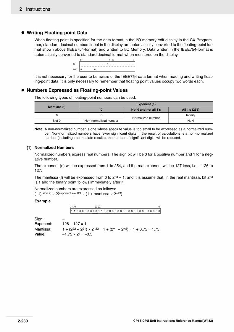
2 Instructions
Writing Floating-point DataWhen floating-point is specified for the data format in the I/O memory edit display in the CX-Program-mer, standard decimal numbers input in the display are automatically converted to the floating-point for-mat shown above (IEEE754-format) and written to I/O Memory. Data written in the IEEE754-format isautomatically converted to standard decimal format when monitored on the display.
It is not necessary for the user to be aware of the IEEE754 data format when reading and writing float-ing-point data. It is only necessary to remember that floating point values occupy two words each.
Numbers Expressed as Floating-point ValuesThe following types of floating-point numbers can be used.
Note A non-normalized number is one whose absolute value is too small to be expressed as a normalized num-ber. Non-normalized numbers have fewer significant digits. If the result of calculations is a non-normalizednumber (including intermediate results), the number of significant digits will be reduced.
(1) Normalized Numbers
Normalized numbers express real numbers. The sign bit will be 0 for a positive number and 1 for a neg-ative number.
The exponent (e) will be expressed from 1 to 254, and the real exponent will be 127 less, i.e., –126 to127.
The mantissa (f) will be expressed from 0 to 233 – 1, and it is assume that, in the real mantissa, bit 233
is 1 and the binary point follows immediately after it.
Normalized numbers are expressed as follows:(–1)(sign s) × 2(exponent e)–127 × (1 + mantissa × 2–23)
Example
Sign: –Exponent: 128 – 127 = 1Mantissa: 1 + (222 + 221) × 2–23 = 1 + (2–1 + 2–2) = 1 + 0.75 = 1.75Value: –1.75 × 21 = –3.5
Mantissa (f)Exponent (e)
0 Not 0 and not all 1’s All 1’s (255)
0 0Normalized number
Infinity
Not 0 Non-normalized number NaN
06715
fn
n+1 s e
1 1 0 0 0 0 0 0 0 0 1 1 0 0 0 0 0 0 0 0 0 0 0 0 0 0 0 0 0 0 0 0 0
31 30 23 22 0
2-230 CP1E CPU Unit Instructions Reference Manual(W483)
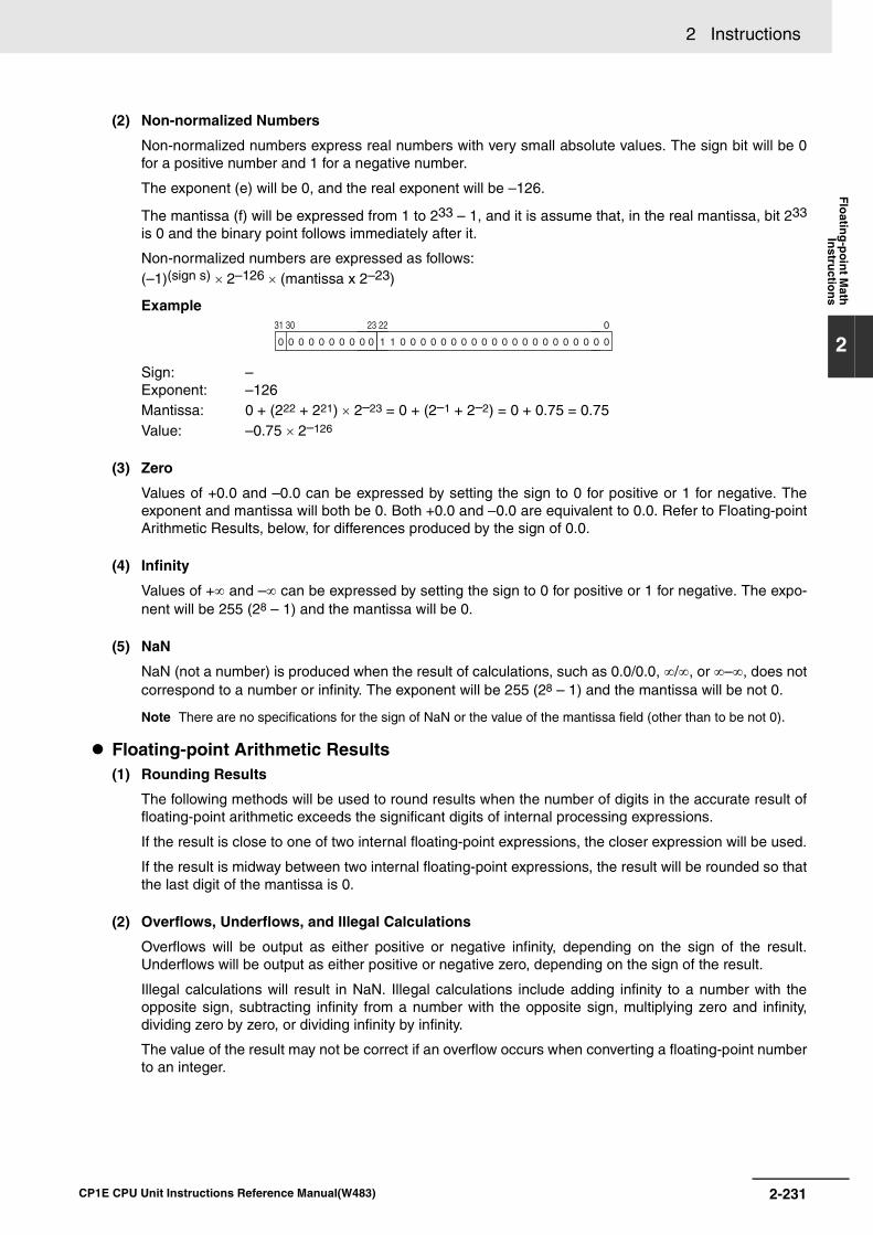
2 Instructions F
loatin
g-p
oin
t Math
Instru
ction
s
2
(2) Non-normalized Numbers
Non-normalized numbers express real numbers with very small absolute values. The sign bit will be 0for a positive number and 1 for a negative number.
The exponent (e) will be 0, and the real exponent will be –126.
The mantissa (f) will be expressed from 1 to 233 – 1, and it is assume that, in the real mantissa, bit 233
is 0 and the binary point follows immediately after it.
Non-normalized numbers are expressed as follows:(–1)(sign s) × 2–126 × (mantissa x 2–23)
Example
Sign: –Exponent: –126Mantissa: 0 + (222 + 221) × 2–23 = 0 + (2–1 + 2–2) = 0 + 0.75 = 0.75Value: –0.75 × 2–126
(3) Zero
Values of +0.0 and –0.0 can be expressed by setting the sign to 0 for positive or 1 for negative. Theexponent and mantissa will both be 0. Both +0.0 and –0.0 are equivalent to 0.0. Refer to Floating-pointArithmetic Results, below, for differences produced by the sign of 0.0.
(4) Infinity
Values of +∞ and –∞ can be expressed by setting the sign to 0 for positive or 1 for negative. The expo-nent will be 255 (28 – 1) and the mantissa will be 0.
(5) NaN
NaN (not a number) is produced when the result of calculations, such as 0.0/0.0, ∞/∞, or ∞–∞, does notcorrespond to a number or infinity. The exponent will be 255 (28 – 1) and the mantissa will be not 0.
Note There are no specifications for the sign of NaN or the value of the mantissa field (other than to be not 0).
Floating-point Arithmetic Results(1) Rounding Results
The following methods will be used to round results when the number of digits in the accurate result offloating-point arithmetic exceeds the significant digits of internal processing expressions.
If the result is close to one of two internal floating-point expressions, the closer expression will be used.
If the result is midway between two internal floating-point expressions, the result will be rounded so thatthe last digit of the mantissa is 0.
(2) Overflows, Underflows, and Illegal Calculations
Overflows will be output as either positive or negative infinity, depending on the sign of the result.Underflows will be output as either positive or negative zero, depending on the sign of the result.
Illegal calculations will result in NaN. Illegal calculations include adding infinity to a number with theopposite sign, subtracting infinity from a number with the opposite sign, multiplying zero and infinity,dividing zero by zero, or dividing infinity by infinity.
The value of the result may not be correct if an overflow occurs when converting a floating-point numberto an integer.
0 0 0 0 0 0 0 0 0 0 1 1 0 0 0 0 0 0 0 0 0 0 0 0 0 0 0 0 0 0 0 0 0
31 30 23 22 0
2-231CP1E CPU Unit Instructions Reference Manual(W483)

2 Instructions
(3) Precautions in Handling Special Values
The following precautions apply to handling zero, infinity, and NaN.
• The sum of positive zero and negative zero is positive zero.
• The difference between zeros of the same sign is positive zero.
• If any operand is a NaN, the Error Flag will be turned ON and the tests will not be executed.
• Positive zero and negative zero are treated as equivalent in comparisons.
• Comparison or equivalency tests on one or more NaN will not be executed and the Error Flag will beturned ON.
Floating-point Calculation ResultsWhen the absolute value of the result is greater than the maximum value that can be expressed forfloating-point data, the Overflow Flag will turn ON and the result will be output as ±∞. If the result is pos-itive, it will be output as +∞; if negative, then –∞.
The Equals Flag will only turn ON when both the exponent (e) and the mantissa (f) are zero after a cal-culation. A calculation result will also be output as zero when the absolute value of the result is lessthan the minimum value that can be expressed for floating-point data. In that case the Underflow Flagwill turn ON.
2-232 CP1E CPU Unit Instructions Reference Manual(W483)

2 Instructions F
loatin
g-p
oin
t Math
Instru
ction
s
2
FIX
/FIX
L
FIX/FIXL
Applicable Program Areas
Operands
Operand Specifications
Flags
Instruction Mnemonic VariationsFunction
codeFunction
FLOATING TO 16-BIT FIX @FIX 450Converts a 32-bit floating-point value to 16-bit signed binary data and places the result in the specified result word.
FLOATING TO 32-BIT FIXL @FIXL 451Converts a 32-bit floating-point value to 32-bit signed binary data and places the result in the specified result words.
Symbol
FIX FIXL
Area Step program areas Subroutines Interrupt tasks
Usage OK OK OK
Operand Description Data type Size
FIX FIXL FIX FIXL
S First source word REAL REAL 2 2
R First result word INT DINT 1 2
Area Word addresses Indirect DM addresses
Constants CF Pulse bits TR bitsCIO WR HR AR T C DM @DM *DM
SOK OK OK OK OK OK OK OK OK
OK--- --- ---
R ---
Name Label Operation
Error Flag P_ER • FIXON if the integer portion of S+1 and S is not within the range of -32,768 to 32,767.
• FIXLON if the integer portion of S+1 and S is not within the range of -2,147,483,648 to 2,147,483,647.
• ON if the data in S+1 and S is not a number (NaN).
• OFF in all other cases.
Equals Flag P_EQ • ON if the result is 0000.
• OFF in all other cases.
Negative Flag P_N • ON when the leftmost bit of the result is 1.
• OFF in all other cases.
S: First source word
R: Result word
FIX(450)
S
R
S: First source word
R: First result word
FIXL(451)
S
R
2-233CP1E CPU Unit Instructions Reference Manual(W483)

2 Instructions
Function FIX
FIX(450) converts the integer portion of the 32-bit floating-point number in S+1 and S (IEEE754-format)to 16-bit signed binary data and places the result in R.
Only the integer portion of the floating-point data is converted, and the fraction portion is truncated.
Example conversions:
A floating-point value of 3.5 is converted to 3.A floating-point value of –3.5 is converted to –3.
FIXLFIXL(451) converts the integer portion of the 32-bit floating-point number in S+1 and S (IEEE754-for-mat) to 32-bit signed binary data and places the result in R+1 and R.
Only the integer portion of the floating-point data is converted, and the fraction portion is truncated.
Example conversions:
A floating-point value of 2,147,483,640.5 is converted to 2,147,483,640.A floating-point value of –214,748,340.5 is converted to –214,748,340.
S+1 S
R
Floating-point data (32 bits)
Signed binary data (16 bits)
S+1 S
R+1 R
Floating-point data (32 bits)
Signed binary data (32 bits)
2-234 CP1E CPU Unit Instructions Reference Manual(W483)
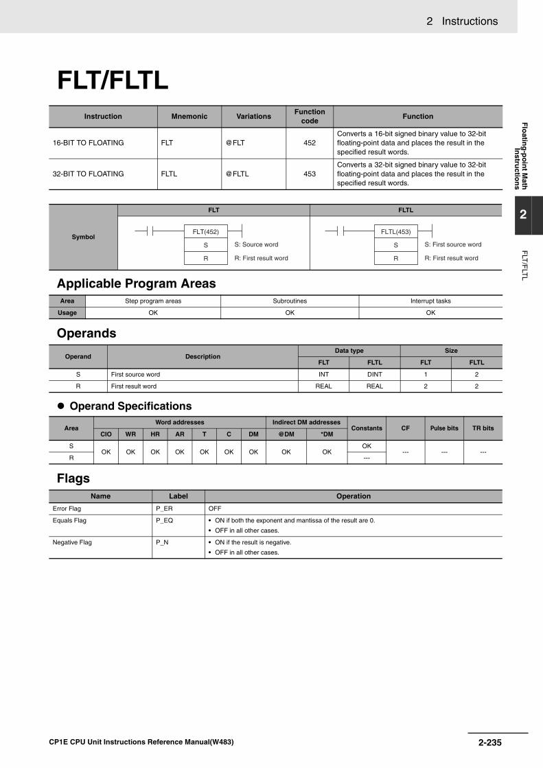
2 Instructions F
loatin
g-p
oin
t Math
Instru
ction
s
2
FLT
/FLT
L
FLT/FLTL
Applicable Program Areas
Operands
Operand Specifications
Flags
Instruction Mnemonic VariationsFunction
codeFunction
16-BIT TO FLOATING FLT @FLT 452Converts a 16-bit signed binary value to 32-bit floating-point data and places the result in the specified result words.
32-BIT TO FLOATING FLTL @FLTL 453Converts a 32-bit signed binary value to 32-bit floating-point data and places the result in the specified result words.
Symbol
FLT FLTL
Area Step program areas Subroutines Interrupt tasks
Usage OK OK OK
Operand DescriptionData type Size
FLT FLTL FLT FLTL
S First source word INT DINT 1 2
R First result word REAL REAL 2 2
Area Word addresses Indirect DM addresses
Constants CF Pulse bits TR bitsCIO WR HR AR T C DM @DM *DM
SOK OK OK OK OK OK OK OK OK
OK--- --- ---
R ---
Name Label Operation
Error Flag P_ER OFF
Equals Flag P_EQ • ON if both the exponent and mantissa of the result are 0.
• OFF in all other cases.
Negative Flag P_N • ON if the result is negative.
• OFF in all other cases.
S: Source word
R: First result word
FLT(452)
S
R
S: First source word
R: First result word
FLTL(453)
S
R
2-235CP1E CPU Unit Instructions Reference Manual(W483)

2 Instructions
Function FLT
FLT(452) converts the 16-bit signed binary value in S to 32-bit floating-point data (IEEE754-format) andplaces the result in R+1 and R. A single 0 is added after the decimal point in the floating-point result.
Only values within the range of -32,768 to 32,767 can be specified for S. To convert signed binary dataoutside of that range, use FLTL(453).
Example conversions:
A signed binary value of 3 is converted to 3.0.A signed binary value of -3 is converted to -3.0.
FLTLFLTL(453) converts the 32-bit signed binary value in S+1 and S to 32-bit floating-point data (IEEE754-format) and places the result in R+1 and R. A single 0 is added after the decimal point in the floating-point result.
Signed binary data within the range of –2,147,483,648 to 2,147,483,647 can be specified for S+1 andS. The floating point value has 24 significant binary digits (bits). The result will not be exact if a numbergreater than 16,777,215 (the maximum value that can be expressed in 24-bits) is converted byFLTL(453).
Example Conversions:
A signed binary value of 16,777,215 is converted to 16,777,215.0.A signed binary value of –16,777,215 is converted to –16,777,215.0.
R+1 R
S
Floating-point data (32 bits)
Signed binary data (16 bits)
R+1: D00101
6 0 E 3B 8 A 3
6 5 1 F 9 2 D1
CY R+1: D00100
8
−
2-236 CP1E CPU Unit Instructions Reference Manual(W483)

2 Instructions F
loatin
g-p
oin
t Math
Instru
ction
s
2
+F, –F, *F, /F
+F, –F, *F, /F
Applicable Program Areas
Operands
Operand Specifications
Instruction Mnemonic VariationsFunction
codeFunction
FLOATING-POINT ADD +F @+F 454Adds two 32-bit floating-point numbers and places the result in the specified result words.
FLOATING-POINT SUBTRACT –F @–F 455Subtracts one 32-bit floating-point number from another and places the result in the specified result words.
FLOATING-POINT MULTIPLY *F @*F 456Multiplies two 32-bit floating-point numbers and places the result in the specified result words.
FLOATING-POINT DIVIDE /F @/F 457Divides one 32-bit floating-point number by another and places the result in the specified result words.
Symbol
+F –F
*F /F
Area Step program areas Subroutines Interrupt tasks
Usage OK OK OK
Operand Description Data type Size
+F Au First augend word
REAL 2AD First addend word
-FMi First Minuend word
REAL 2Su First Subtrahend word
*F Md First Multiplicand word
REAL 2Mr First Multiplier word
/FDd First Dividend word
REAL 2Dr First Divisor word
R First result word REAL 2
Area Word addresses Indirect DM addresses
Constants CF Pulse bits TR bitsCIO WR HR AR T C DM @DM *DM
Au, AD, Mi, Su, Md, Mr, Dd, Dr OK OK OK OK OK OK OK OK OK
OK--- --- ---
R ---
Au: First augend word
AD: First addend word
R: First result word
+F(454)
Au
AD
R
Mi: First Minuend word
Su: First Subtrahend word
R: First result word
–F(455)
Mi
Su
R
Md: First Multiplicand word
Mr: First Multiplier word
R: First result word
*F(456)
Md
Mr
R
Dd: First Dividend word
Dr: First Divisor word
R: First result word
/F(457)
Dd
Dr
R
2-237CP1E CPU Unit Instructions Reference Manual(W483)

2 Instructions
Flags
FunctionThe data specified in Au/Mi/Md/Dd and the data specified in AD/Su/Mr/Dr are added (+F), subtracted (-F), multiplied (*F), or divided (/F) as single-precision floating-point data (32 bits: IEEE754) and outputto R+1, R.
+F
-F
Name Label Operation
Error Flag P_ER +F
• ON if the augend or addend data is not a number (NaN).
• ON if +∞ and –∞ are added.
-F
• ON if the minuend or subtrahend is not a number (NaN).
• ON if +∞ is subtracted from +∞.
• ON if –∞ is subtracted from –∞.
*F
• ON if the multiplicand or multiplier is not a number (NaN).
• ON if +∞ and 0 are multiplied.
• ON if –∞ and 0 are multiplied.
/F
• ON if the dividend or divisor is not a number (NaN).
• ON if the dividend and divisor are both 0.
• ON if the dividend and divisor are both +∞ or –∞.
OFF in all other cases.
Equals Flag P_EQ • ON if both the exponent and mantissa of the result are 0.
• OFF in all other cases.
Overflow Flag P_OF • ON if the absolute value of the result is too large to be expressed as a 32-bit floating-point value.
• OFF in all other cases.
Underflow Flag P_UF • ON if the absolute value of the result is too small to be expressed as a 32-bit floating-point value.
• OFF in all other cases.
Negative Flag P_N • ON if the result is negative.
• OFF in all other cases.
R+1 R
+
AuAu+1
AdAd+1
Result (floating-point data, 32 bits)
Augend (floating-point data, 32 bits)
Addend (floating-point data, 32 bits)
R+1 R
–
MiMi+1
SuSu+1
Result (floating-point data, 32 bits)
Subtrahend (floating-point data, 32 bits)
Minuend (floating-point data, 32 bits)
2-238 CP1E CPU Unit Instructions Reference Manual(W483)

2 Instructions F
loatin
g-p
oin
t Math
Instru
ction
s
2
+F, –F, *F, /F
*F
/F
• If the absolute value of the result is greater than the maximum value that can be expressed as float-ing-point data, the Overflow Flag will turn ON and the result will be output as ±∞.
• If the absolute value of the result is less than the minimum value that can be expressed as floating-point data, the Underflow Flag will turn ON and the result will be output as 0.
Operation rulesThe result of an operation is output as shown below depending on the combination of floating-pointdata.
FLOATING-POINT ADD (+F)
Note 1 The results could be zero (including underflows), a numeral, +∞, or –∞.
ER The Error Flag will be turned ON and the instruction will not be executed.
FLOATING-POINT SUBTRACT (–F)
Note 1 The results could be zero (including underflows), a numeral, +∞, or –∞.
ER The Error Flag will be turned ON and the instruction will not be executed.
Augend
Addend 0 Numeral +∞ –∞ NaN
0 0 Numeral +∞ –∞
Numeral Numeral See note 1. +∞ –∞
+∞ +∞ +∞ +∞ ER
–∞ –∞ –∞ ER –∞
NaN ER
Minuend
Subtrahend 0 Numeral +∞ –∞ NaN
0 0 Numeral +∞ –∞
Numeral Numeral See note 1. +∞ –∞
+∞ –∞ –∞ ER –∞
–∞ +∞ +∞ +∞ ER
NaN ER
R+1 R
Md Multiplicand (floating-point data, 32 bits)Md+1
Mr Multiplier (floating-point data, 32 bits)Mr+1
Result (floating-point data, 32 bits)
×
R+1 R
÷
Dd Dividend (floating-point data, 32 bits)Dd+1
Dr Divisor (floating-point data, 32 bits)Dr+1
Result (floating-point data, 32 bits)
2-239CP1E CPU Unit Instructions Reference Manual(W483)
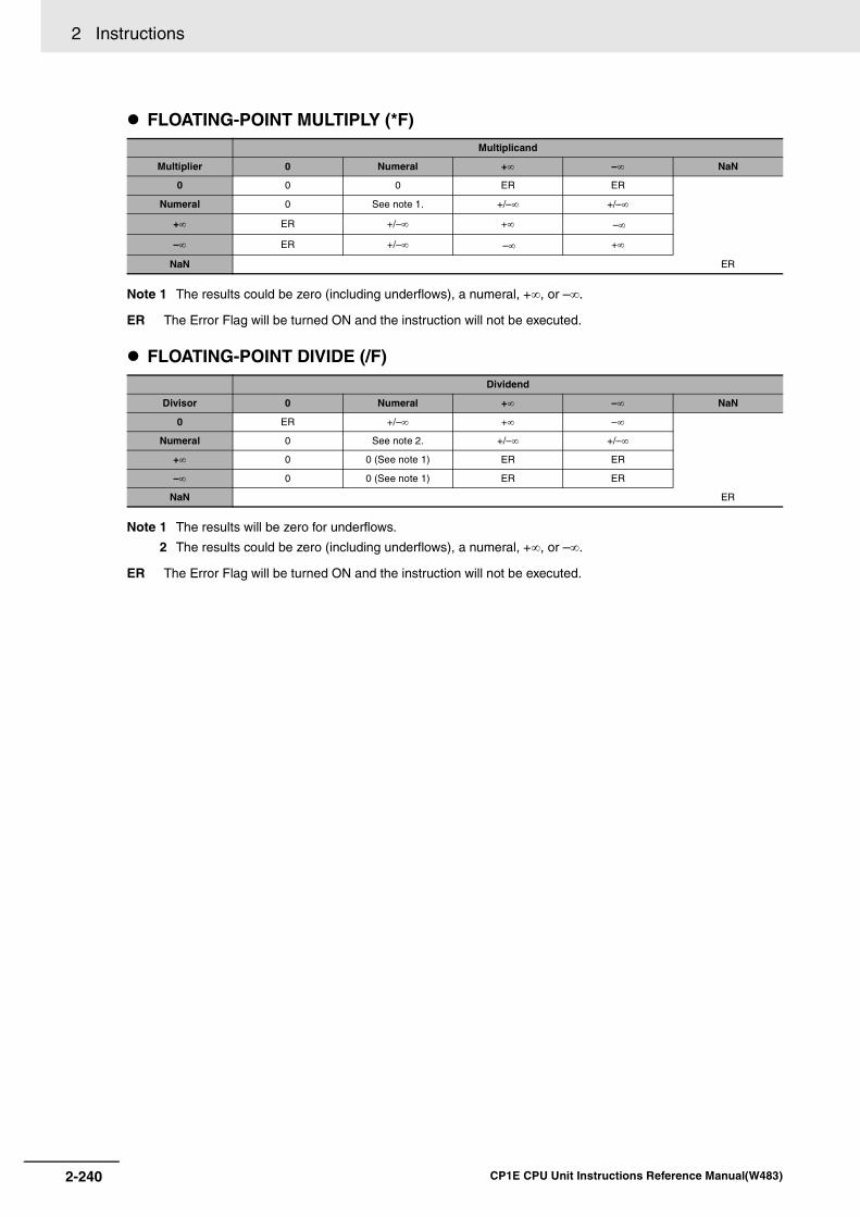
2 Instructions
FLOATING-POINT MULTIPLY (*F)
Note 1 The results could be zero (including underflows), a numeral, +∞, or –∞.
ER The Error Flag will be turned ON and the instruction will not be executed.
FLOATING-POINT DIVIDE (/F)
Note 1 The results will be zero for underflows.
2 The results could be zero (including underflows), a numeral, +∞, or –∞.
ER The Error Flag will be turned ON and the instruction will not be executed.
Multiplicand
Multiplier 0 Numeral +∞ –∞ NaN
0 0 0 ER ER
Numeral 0 See note 1. +/–∞ +/–∞
+∞ ER +/–∞ +∞ –∞
–∞ ER +/–∞ –∞ +∞
NaN ER
Dividend
Divisor 0 Numeral +∞ –∞ NaN
0 ER +/–∞ +∞ –∞
Numeral 0 See note 2. +/–∞ +/–∞
+∞ 0 0 (See note 1) ER ER
–∞ 0 0 (See note 1) ER ER
NaN ER
2-240 CP1E CPU Unit Instructions Reference Manual(W483)
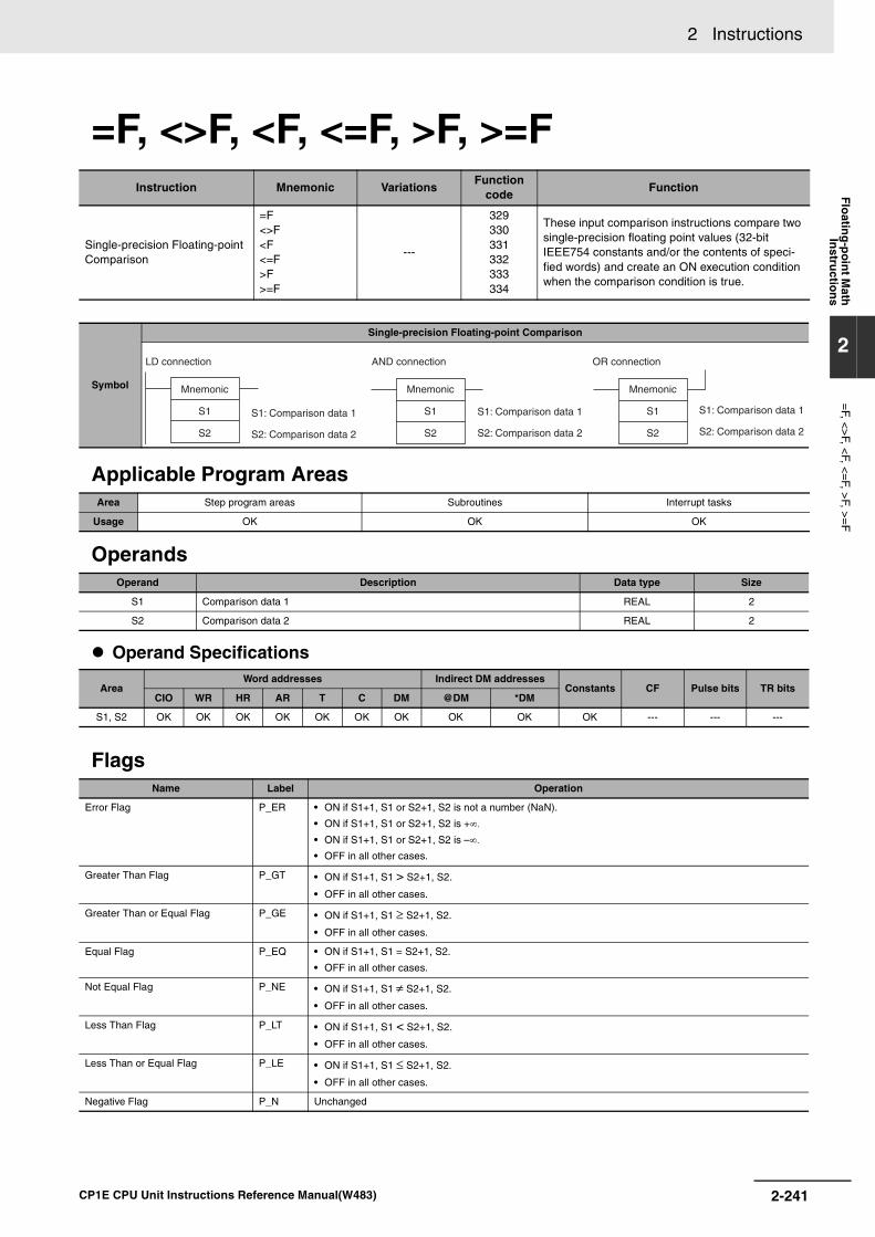
2 Instructions F
loatin
g-p
oin
t Math
Instru
ction
s
2
=F, <
>F, <
F, <=F, >
F, >=
F
=F, <>F, <F, <=F, >F, >=F
Applicable Program Areas
Operands
Operand Specifications
Flags
Instruction Mnemonic VariationsFunction
codeFunction
Single-precision Floating-point Comparison
=F<>F<F<=F>F>=F
---
329330331332333334
These input comparison instructions compare two single-precision floating point values (32-bit IEEE754 constants and/or the contents of speci-fied words) and create an ON execution condition when the comparison condition is true.
Symbol
Single-precision Floating-point Comparison
Area Step program areas Subroutines Interrupt tasks
Usage OK OK OK
Operand Description Data type Size
S1 Comparison data 1 REAL 2
S2 Comparison data 2 REAL 2
Area Word addresses Indirect DM addresses
Constants CF Pulse bits TR bitsCIO WR HR AR T C DM @DM *DM
S1, S2 OK OK OK OK OK OK OK OK OK OK --- --- ---
Name Label Operation
Error Flag P_ER • ON if S1+1, S1 or S2+1, S2 is not a number (NaN).
• ON if S1+1, S1 or S2+1, S2 is +∞.
• ON if S1+1, S1 or S2+1, S2 is –∞.
• OFF in all other cases.
Greater Than Flag P_GT • ON if S1+1, S1 > S2+1, S2.
• OFF in all other cases.
Greater Than or Equal Flag P_GE • ON if S1+1, S1 ≥ S2+1, S2.
• OFF in all other cases.
Equal Flag P_EQ • ON if S1+1, S1 = S2+1, S2.
• OFF in all other cases.
Not Equal Flag P_NE • ON if S1+1, S1 ≠ S2+1, S2.
• OFF in all other cases.
Less Than Flag P_LT • ON if S1+1, S1 < S2+1, S2.
• OFF in all other cases.
Less Than or Equal Flag P_LE • ON if S1+1, S1 ≤ S2+1, S2.
• OFF in all other cases.
Negative Flag P_N Unchanged
S2: Comparison data 2
LD connection AND connection OR connection
S1: Comparison data 1
S2: Comparison data 2
S1: Comparison data 1
S2: Comparison data 2
S1: Comparison data 1
Mnemonic
S1
S2
Mnemonic
S1
S2
Mnemonic
S1
S2
2-241CP1E CPU Unit Instructions Reference Manual(W483)

2 Instructions
Function
Options
With the three input types and six symbols, there are 18 different possible combinations.
The input comparison instructioncompares the data specified in S1and S2 as single-precision floatingpoint values (32-bit IEEE754 data)and creates an ON execution condi-tion when the comparison conditionis true. When the data is stored in words, S1and S2 specify the first of two wordscontaining the 32-bit data. It is alsopossible to input the floating-pointdata as an 8-digit hexadecimal con-stant.
The input comparison instructionsare treated just like the LD, AND, andOR instructions to control the execu-tion of subsequent instructions.
LD: The instruction can be con-nected directly to the left bus bar.
AND: The instruction cannot be con-nected directly to the left bus bar.
OR: The instruction can be con-nected directly to the left bus bar.
Symbol (LD, AND, and OR cannot be
used in a ladder program)Option (data format)
LD=, AND=, OR=, LD<>, AND<>, OR<>, LD<, AND<, OR<, LD<=, AND<=, OR<=, LD>, AND>, OR>, LD>=, AND>=, OR>=
+ F: Single-precision floating-point data
Code Mnemonic Name Function
329 LD=F LOAD FLOATING EQUAL True ifS1+1, S1 = S2+1, S2
AND=F AND FLOATING EQUAL
OR=F OR FLOATING EQUAL
330 LD<>F LOAD FLOATING NOT EQUAL True ifS1+1, S1≠ S2+1, S2
AND<>F AND FLOATING NOT EQUAL
OR<>F OR FLOATING NOT EQUAL
331 LD<F LOAD FLOATING LESS THAN True ifS1+1, S1 < S2+1, S2
AND<F AND FLOATING LESS THAN
OR<F OR FLOATING LESS THAN
332 LD<=F LOAD FLOATING LESS THAN OR EQUAL True ifS1+1, S1 ≤ S2+1, S2
AND<=F AND FLOATING LESS THAN OR EQUAL
OR<=F OR FLOATING LESS THAN OR EQUAL
333 LD>F LOAD FLOATING GREATER THAN True ifS1+1, S1 > S2+1, S2
AND>F AND FLOATING GREATER THAN
OR>F OR FLOATING GREATER THAN
<F
S1
S2
<F
S1
S2
<F
S1
S2
LD connection
AND connection
OR connection
ON execution condition when comparison result is true.
ON execution condition when comparison result is true.
ON execution condition when comparison result is true.
2-242 CP1E CPU Unit Instructions Reference Manual(W483)
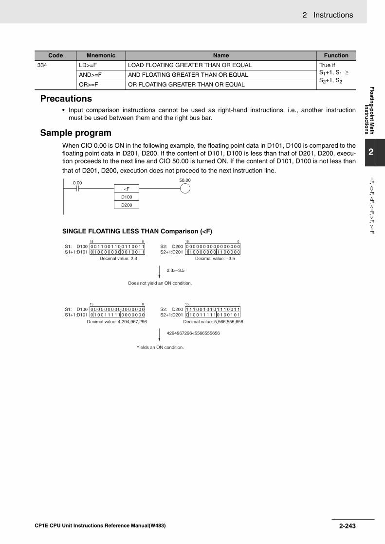
2 Instructions F
loatin
g-p
oin
t Math
Instru
ction
s
2
=F, <
>F, <
F, <=F, >
F, >=
F
Precautions• Input comparison instructions cannot be used as right-hand instructions, i.e., another instruction
must be used between them and the right bus bar.
Sample programWhen CIO 0.00 is ON in the following example, the floating point data in D101, D100 is compared to thefloating point data in D201, D200. If the content of D101, D100 is less than that of D201, D200, execu-tion proceeds to the next line and CIO 50.00 is turned ON. If the content of D101, D100 is not less than
that of D201, D200, execution does not proceed to the next instruction line.
SINGLE FLOATING LESS THAN Comparison (<F)
334 LD>=F LOAD FLOATING GREATER THAN OR EQUAL True ifS1+1, S1 ≥ S2+1, S2
AND>=F AND FLOATING GREATER THAN OR EQUAL
OR>=F OR FLOATING GREATER THAN OR EQUAL
Code Mnemonic Name Function
<F
D100
D200
0.00 50.00
2.3>−3.5
0 0 0 0 0 0 0 0 0 0 0 0 0 0 0 01 1 0 0 0 0 0 0 0 1 1 0 0 0 0 0
15 0
0 0 1 1 0 0 1 1 0 0 1 1 0 0 1 10 1 0 0 0 0 0 0 0 0 0 1 0 0 1 1
15 0
S1: D100S1+1:D101
S2: D200S2+1:D201
4294967296<5566555656
1 1 1 0 0 1 0 1 0 1 1 1 0 0 1 10 1 0 0 1 1 1 1 1 0 1 0 0 1 0 1
15
0 0 0 0 0 0 0 0 0 0 0 0 0 0 0 00 1 0 0 1 1 1 1 1 0 0 0 0 0 0 0
15 0
S1: D100S1+1:D101
S2: D200S2+1:D201
Does not yield an ON condition.
Decimal value: 2.3 Decimal value: −3.5
Decimal value: 5,566,555,656Decimal value: 4,294,967,296
Yields an ON condition.
2-243CP1E CPU Unit Instructions Reference Manual(W483)

2 Instructions
FSTR
Applicable Program Areas
Operands
C: First Control Word
Operand Specifications
Flags
Instruction Mnemonic VariationsFunction
codeFunction
FLOATING-POINT TO ASCII FSTR @FSTR 448Expresses a 32-bit floating-point value (IEEE754-format) in standard decimal notation or scientific notation and converts that value to ASCII text.
Symbol
FSTR
Area Step program areas Subroutines Interrupt tasks
Usage OK OK OK
Operand Description Data type Size
S First source word REAL 2
C First control word UINT 3
D First destination word UINT Variable
Area Word addresses Indirect DM addresses
Constants CF Pulse bits TR bitsCIO WR HR AR T C DM @DM *DM
SOK OK OK OK OK OK OK OK OK
OK--- --- ---
C, D ---
Name Label Operation
Error Flag P_ER • ON if the data in S+1 and S is not a valid floating-point number (NaN).
• ON if the data in S+1 and S is +o or -o.
• ON if the Data Format setting in C is not 0000 or 0001.
• ON if the Total Characters setting in C+1 is not within the allowed range. (See 1. Limits on the Total Number of ASCII Characters above for details.)
• ON if the Fractional Digits setting in C+2 is not within the allowed range. (See 3. Limits on the Number of Digits in the Fractional Part above for details.)
Equals Flag P_EQ • ON if the conversion result is 0.
• OFF in all other cases.
D: First destination word
FSTR(448)
S
C
D
C: First control word
S: First source word
0 hex: Decimal format
1 hex: Scientific notation
2 to 18 hex (2 to 24 characters, see note)
0 to 7 hex (see note)
Note There are limits on the total number of charactersand the number of fractional digits.
Data format
Total characters
Fractional digits
2-244 CP1E CPU Unit Instructions Reference Manual(W483)
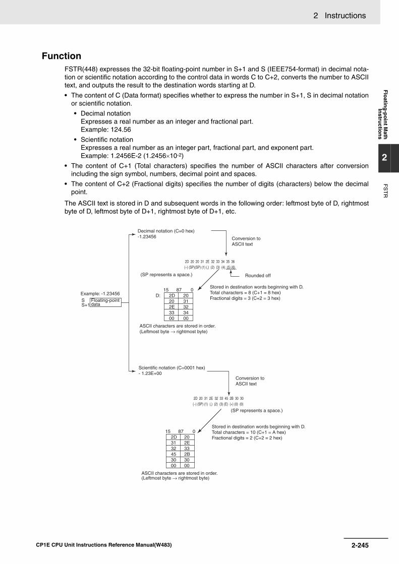
2 Instructions F
loatin
g-p
oin
t Math
Instru
ction
s
2
FS
TR
FunctionFSTR(448) expresses the 32-bit floating-point number in S+1 and S (IEEE754-format) in decimal nota-tion or scientific notation according to the control data in words C to C+2, converts the number to ASCIItext, and outputs the result to the destination words starting at D.
• The content of C (Data format) specifies whether to express the number in S+1, S in decimal notationor scientific notation.
• Decimal notationExpresses a real number as an integer and fractional part.Example: 124.56
• Scientific notationExpresses a real number as an integer part, fractional part, and exponent part.Example: 1.2456E-2 (1.2456×10⁻²)
• The content of C+1 (Total characters) specifies the number of ASCII characters after conversionincluding the sign symbol, numbers, decimal point and spaces.
• The content of C+2 (Fractional digits) specifies the number of digits (characters) below the decimalpoint.
The ASCII text is stored in D and subsequent words in the following order: leftmost byte of D, rightmostbyte of D, leftmost byte of D+1, rightmost byte of D+1, etc.
SS+1
15 87 0
15 87 0
D: 2031323400
2D202E3300
202E332B3000
2D3132453000
Decimal notation (C=0 hex)-1.23456
Example: -1.23456Floating-point data
Stored in destination words beginning with D.Total characters = 10 (C+1 = A hex)Fractional digits = 2 (C+2 = 2 hex)
Scientific notation (C=0001 hex)- 1.23E+00
Stored in destination words beginning with D.Total characters = 8 (C+1 = 8 hex)Fractional digits = 3 (C+2 = 3 hex)
Conversion to ASCII text
Conversion to ASCII text
Rounded off
ASCII characters are stored in order. (Leftmost byte → rightmost byte)
(SP represents a space.)
(SP represents a space.)
ASCII characters are stored in order. (Leftmost byte → rightmost byte)
2-245CP1E CPU Unit Instructions Reference Manual(W483)

2 Instructions
Storage of ASCII TextAfter the floating-point number is converted to ASCII text, the ASCII characters are stored in the desti-nation words beginning with D, as shown in the following diagrams. Different storage methods are usedfor decimal notation and scientific notation.
Note Either one or two bytes of zeroes are added to the end of ASCII text as an end code.
• Total number of characters odd: 00 hex is stored after the ASCII text.
• Total number of characters even: 0000 hex is stored after the ASCII text.
Limits on the Number of ASCII CharactersThere are limits on the number of ASCII characters in the converted number. The Error Flag will beturned ON if the number of characters exceeds the maximum allowed.
• Limits on the Total Number of ASCII Characters
1) Decimal Notation (C = 0 hex)
• When there is no fractional part (C+2 = 0 hex):2 ≤ Total Characters ≤ 24
• When there is a fractional part (C+2 = 1 to 7 hex):(Fractional digits + 3) ≤ Total Characters ≤ 24
2) Scientific Notation (C = 1 hex)
• When there is no fractional part (C+2 = 0 hex):6 ≤ Total Characters ≤ 24
• When there is a fractional part (C+2 = 1 to 7 hex):(Fractional digits + 7) ≤ Total Characters ≤ 24
Total number of characters
Integer part Fractional partSign Decimal point
If there are more fractional digits in the source data than specified in C+1, the extra digits will be rounded off. If there are fewer fractional digits, zeroes (ASCII: 30 hex) will added to the end of the source data.
A decimal point (ASCII: 2E hex) is added if the number fractional digits is greater than 0.Spaces (ASCII: 20 hex) are added if the integer part of the floating-point data is shorter than the integer part of the result (total number of characters - sign digit - decimal point - fractional digits).
Positive number: Space (20 hex)Negative number: Minus sign (2D hex)
Decimal notation (C=0 hex)
Scientific notation (C=1 hex)
Total number of characters Total number of characters
E
Total number of characters
Integer part Fractional part Exponential partSign Decimal point Sign
0 to 9 are written as 00 to 09.Positive: Plus sign (2B hex)Negative: Minus sign (2D hex)
Letter E (ASCII: 45 hex) is written here.If there are more fractional digits in the source data than specified in C+1, the extra digits will be rounded off. If there are fewer fractional digits, zeroes (ASCII: 30 hex) will added to the end of the source data.
A decimal point (ASCII: 2E hex) is added if the number fractional digits is greater than 0.Spaces (ASCII: 20 hex) are added if the integer part of the floating-point data is shorter than the integer part of the result (total number of characters - sign digit - decimal point - fractional digits - E digit).
Positive number: Space (20 hex)Negative number: Minus sign (2D hex)
2-246 CP1E CPU Unit Instructions Reference Manual(W483)
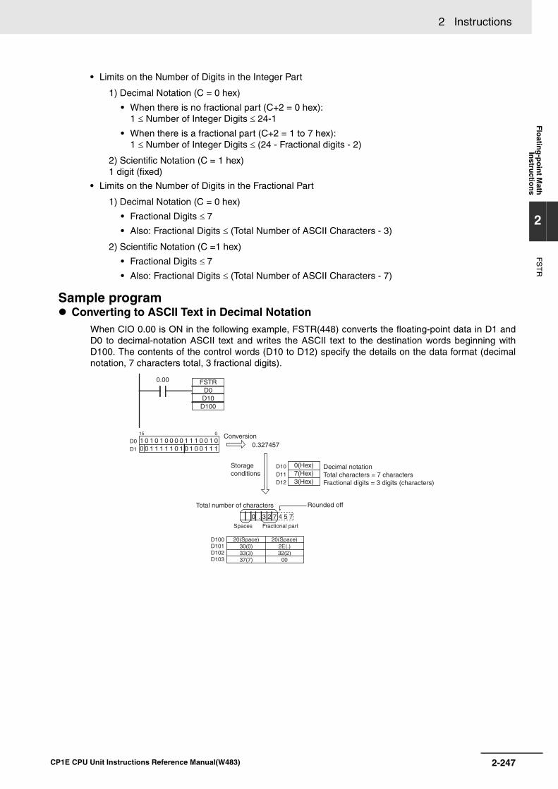
2 Instructions F
loatin
g-p
oin
t Math
Instru
ction
s
2
FS
TR
• Limits on the Number of Digits in the Integer Part
1) Decimal Notation (C = 0 hex)
• When there is no fractional part (C+2 = 0 hex):1 ≤ Number of Integer Digits ≤ 24-1
• When there is a fractional part (C+2 = 1 to 7 hex):1 ≤ Number of Integer Digits ≤ (24 - Fractional digits - 2)
2) Scientific Notation (C = 1 hex)1 digit (fixed)
• Limits on the Number of Digits in the Fractional Part
1) Decimal Notation (C = 0 hex)
• Fractional Digits ≤ 7
• Also: Fractional Digits ≤ (Total Number of ASCII Characters - 3)
2) Scientific Notation (C =1 hex)
• Fractional Digits ≤ 7
• Also: Fractional Digits ≤ (Total Number of ASCII Characters - 7)
Sample program Converting to ASCII Text in Decimal Notation
When CIO 0.00 is ON in the following example, FSTR(448) converts the floating-point data in D1 andD0 to decimal-notation ASCII text and writes the ASCII text to the destination words beginning withD100. The contents of the control words (D10 to D12) specify the details on the data format (decimalnotation, 7 characters total, 3 fractional digits).
20(Space)2E(.)32(2)
00
1 0 1 0 1 0 0 0 0 1 1 1 0 0 1 00 0 1 1 1 1 1 0 1 0 1 0 0 1 1 1
0.00
15 0
D0D1
0(Hex)7(Hex)3(Hex)
D10D11D12
0.327457
20(Space)30(0)33(3)37(7)
D100D101D102D103
0 . 3 2 7 4 5 7
FSTRD0
D10D100
Conversion
Storage conditions
Decimal notationTotal characters = 7 charactersFractional digits = 3 digits (characters)
Total number of characters Rounded off
Spaces Fractional part
2-247CP1E CPU Unit Instructions Reference Manual(W483)

2 Instructions
Converting to ASCII Text in Scientific NotationWhen CIO 0.00 is ON in the following example, FSTR(448) converts the floating-point data in D1 andD0 to scientific-notation ASCII text and writes the ASCII text to the destination words beginning withD100. The contents of the control words (D10 to D12) specify the details on the data format (scientificnotation, 11 characters total, 3 fractional digits).
20(Space)2E(.)37(7)45(E)30(0)
00
1 0 1 0 1 0 0 0 0 1 1 1 0 0 1 00 0 1 1 1 1 1 0 1 0 1 0 0 1 1 1
0.00
15 0
D0D1
0001(Hex)000B(Hex)0003(Hex)
D10D11D12
0.327457
20(Space)33(3)32(2)35(5)2D(-)31(1)
D100D101D102D103D104D105
3 . 2 7 4 5 7 E - 0 1
FSTRD0
D10D100
Conversion
Storage conditions
Scientific notationTotal characters = 11 charactersFractional digits = 3 digits (characters)
Total number of characters
Spaces Fractional part Rounded off
2-248 CP1E CPU Unit Instructions Reference Manual(W483)

2 Instructions F
loatin
g-p
oin
t Math
Instru
ction
s
2
FV
AL
FVAL
Applicable Program Areas
Operands
Operand Specifications
Flags
FunctionFVAL(449) converts the specified ASCII text number (starting at word S) to a 32-bit floating-point num-ber (IEEE754-format) and outputs the result to the destination words starting at D.
FVAL(449) can convert ASCII text in decimal or scientific notation if it meets the following conditions:
Up to 6 characters are valid, excluding the sign, decimal point, and exponent. Any characters beyondthe 6th character will be ignored.
• Decimal NotationReal numbers expressed with an integer and fractional part.Example: 124.56
Instruction Mnemonic VariationsFunction
codeFunction
ASCII TO FLOATING-POINT FVAL @FVAL 449
Converts a number expressed in ASCII text (deci-mal or scientific notation) to a 32-bit floating-point value (IEEE754-format) and outputs the floating-point value to the specified words.
Symbol
FVAL
Area Step program areas Subroutines Interrupt tasks
Usage OK OK OK
Operand Description Data type Size
S First source word UINT Variable
D First destination word REAL 2
Area Word addresses Indirect DM addresses
Constants CFPulse bits
TR bitsCIO WR HR AR T C DM @DM *DM
S, D OK OK OK OK OK OK OK OK OK --- --- --- ---
Name Label Operation
Error Flag P_ER • ON if the digits (integer and fractional parts) in the source data starting at S are not 30 to 39 hex (0 to 9).
• ON if the first two digits of the exponential part do not contain 45 and 2B hex (E+) or 45 and 2D hex (E-). in the source data starting at S are not 30 to 39 hex (0 to 9).
• ON if there are two or more exponential parts in the source data.
• ON if the data is +∞ or -∞ after conversion.
• ON if there are 0 characters in the text data.
• ON if a byte containing 00 hex is not found within the first 25 characters.
• OFF in all other cases.
Equals Flag P_EQ • ON if the conversion result is 0.
• OFF in all other cases.
S: First source word
D: First destination word
FVAL(449)
S
D
2-249CP1E CPU Unit Instructions Reference Manual(W483)
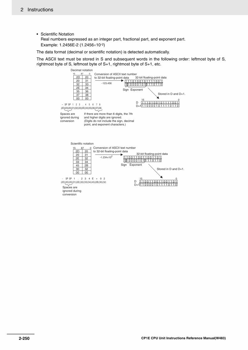
2 Instructions
• Scientific NotationReal numbers expressed as an integer part, fractional part, and exponent part.Example: 1.2456E-2 (1.2456×10⁻²)
The data format (decimal or scientific notation) is detected automatically.
The ASCII text must be stored in S and subsequent words in the following order: leftmost byte of S,rightmost byte of S, leftmost byte of S+1, rightmost byte of S+1, etc.
Conversion of ASCII text number to 32-bit floating-point data 32-bit floating-point data
Sign Exponent
Stored in D and D+1.
2D 2020 3132 332E 3435 3637 3800 00
15 87 0
1 1 1 0 1 0 0 1 0 1 1 1 1 0 0 11 1 0 0 0 0 1 0 1 1 1 1 0 1 1 0
DD+1
1 1 1 0 1 0 0 1 0 1 1 1 1 0 0 11 1 0 0 0 0 1 0 1 1 1 1 0 1 1 0
15 0
Spaces are ignored during conversion
If there are more than 6 digits, the 7th and higher digits are ignored.(Digits do not include the sign, decimal point, and exponent characters.)
Decimat notation
2D202E33453000
203132342B3200
− SP SP 1 . 2 3 4 E + 0 2(2D)(20)(20)(31)(2E)(32)(33)(34)(45)(2B)(30)(32)
-1.234×10² 1 1 0 0 1 1 0 0 1 1 0 0 1 1 0 11 1 0 0 0 0 1 0 1 1 1 1 0 1 1 0
DD+1
1 1 0 0 1 1 0 0 1 1 0 0 1 1 0 11 1 0 0 0 0 1 0 1 1 1 1 0 1 1 0
15 0
15 87 0
Spaces are ignored during conversion
Conversion of ASCII text number to 32-bit floating-point data
Scientific notation
32-bit floating-point data
Sign Exponent
Stored in D and D+1.
2-250 CP1E CPU Unit Instructions Reference Manual(W483)

2 Instructions F
loatin
g-p
oin
t Math
Instru
ction
s
2
FV
AL
Storage of ASCII TextThe following diagrams show how the ASCII text number is converted to floating-point data. Differentconversion methods are used for numbers stored with decimal notation and scientific notation.
00
S FVAL(449) converts the ASCII characters starting with the leftmost byte of S and continuing until a byte containing 00 hex is reached. There must be a byte containing 00 hex within the first 25 bytes.
Up to 00 hex(25 characters max.)
15 078
00SP SP
(20)
Digit
Sign
(20)
00
25 characters max
Integer part Fractional partSign
Decimal point The 7th and higher digits are ignored. (The sign, decimal point,
and exponent characters are not counted as digits.)
Any spaces (20 hex) or zeroes (30 hex) before the first digit are ignored.
Positive number: Space (20 hex) or Plus sign (2B hex)Negative number: Minus sign (2D hex)
.
Decimal notation
15 078
(20)
Digit
Digit
...
Sign
Digit
00SP E
Sign
(20)
.(2E)
Digit
E(45)
Digit
00
25 characters max.
Integer part Fractional part Exponential part
Decimal point
SignSign
Positive: + (2B hex)Negative: - (2D hex)E (45)
The 7th and higher digits are ignored.(The sign, decimal point, and exponent characters are not counted as digits.)
Any spaces (20 hex) or zeroes (30 hex) before the first digit are ignored.
Positive number: Space (20 hex) or Plus sign (2B hex)Negative number: Minus sign (2D hex)
.
Scientific notation
ASCII Character Storage
2-251CP1E CPU Unit Instructions Reference Manual(W483)

2 Instructions
Sample program Converting ASCII Text in Decimal Notation to Floating-point Data
When CIO 0.00 is ON in the following example, FVAL(449) converts the specified decimal-notationASCII text number in the source words starting at D0 to floating-point data and writes the result to des-tination words D100 and D101.
Converting ASCII Text in Scientific NotationWhen CIO 0.00 is ON in the following example, FVAL(449) converts the specified scientific-notationASCII text number in the source words starting at D0 to floating-point data and writes the result to des-tination words D100 and D101.
0 0 0 0 0 1 0 0 1 1 0 0 0 0 0 01 0 1 1 1 1 1 1 1 0 0 1 1 1 1 0
0.00
15 0
D100D101
20 (Space)31 (1)32 (2)34 (4)32 (2)
00
D0D1D2D3D4D5
0 0 0 0 0 1 0 0 1 1 0 0 0 0 0 01 0 1 1 1 1 1 1 1 0 0 1 1 1 1 0
15 0
FVALD0
D100
The 7th and higher digits are ignored.(The sign, decimal point, and leading zeroes/spaces are not counted.)Ignored
Conversion
Storage
0 1 0 0 0 0 1 0 1 0 1 0 1 1 1 11 0 1 1 1 1 0 0 0 1 0 0 1 0 1 0
0.00
15 0
D100D101
D0D1D2D3D4D5D6
0 1 0 0 0 0 1 0 1 0 1 0 1 1 1 11 0 1 1 1 1 0 0 0 1 0 0 1 0 1 0
15 0
FVALD0
D100
1 . 2 3 4 5 E - 0 2
Ignored Ignored
Conversion
Storage
20 (Space)
2-252 CP1E CPU Unit Instructions Reference Manual(W483)
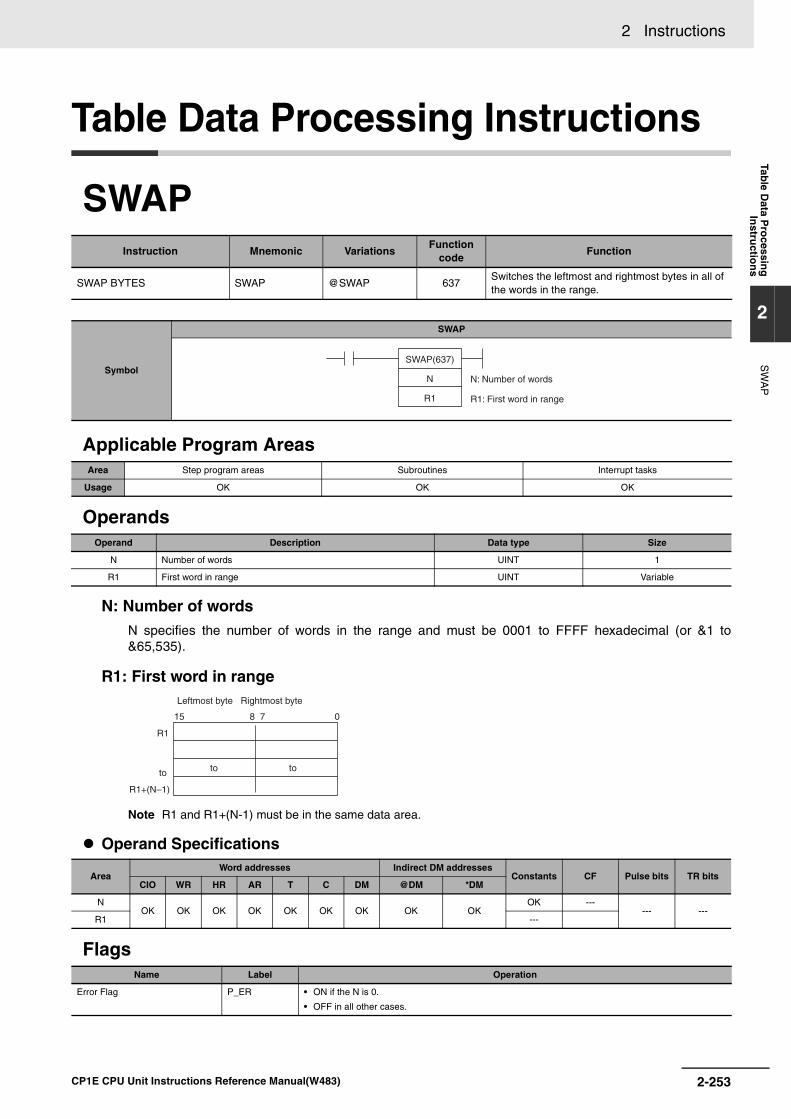
2 Instructions Tab
le Data P
rocessin
gIn
structio
ns
2
SW
AP
Table Data Processing Instructions
SWAP
Applicable Program Areas
Operands
N: Number of wordsN specifies the number of words in the range and must be 0001 to FFFF hexadecimal (or &1 to&65,535).
R1: First word in range
Note R1 and R1+(N-1) must be in the same data area.
Operand Specifications
Flags
Instruction Mnemonic VariationsFunction
codeFunction
SWAP BYTES SWAP @SWAP 637Switches the leftmost and rightmost bytes in all of the words in the range.
Symbol
SWAP
Area Step program areas Subroutines Interrupt tasks
Usage OK OK OK
Operand Description Data type Size
N Number of words UINT 1
R1 First word in range UINT Variable
Area Word addresses Indirect DM addresses
Constants CF Pulse bits TR bitsCIO WR HR AR T C DM @DM *DM
NOK OK OK OK OK OK OK OK OK
OK ------ ---
R1 ---
Name Label Operation
Error Flag P_ER • ON if the N is 0.
• OFF in all other cases.
N: Number of words
R1: First word in range
SWAP(637)
N
R1
R1
R1+(N–1)
15 08 7
to to to
Leftmost byte Rightmost byte
2-253CP1E CPU Unit Instructions Reference Manual(W483)

2 Instructions
FunctionSWAP(637) switches the position of the twobytes in all of the words in the range of mem-ory from R1 to R1+N-1.
Hint• This instruction can be used to reverse the order of ASCII-code characters in each word.
Sample programWhen CIO 0.00 is ON in the following example, SWAP(637) switches the data in the leftmost bytes withthe data in the rightmost bytes in each word in the 10-word range from W0 to W9.
N
R1
Byte position is swapped.
SWAP
&10
W0
07815
4 1 4 2
4 3 4 4
4 5 4 6
3 0 3 1
07815
4 2 4 1
4 4 4 3
4 6 4 5
3 1 3 0
W0
W1
W2
to
W9
W0
W1
W2
to
W9
N
R1
to to
0.00
2-254 CP1E CPU Unit Instructions Reference Manual(W483)

2 Instructions Tab
le Data P
rocessin
gIn
structio
ns
2
FC
S
FCS
Applicable Program Areas
Operands
Operand Specifications
Flags
Instruction Mnemonic VariationsFunction
codeFunction
FRAME CHECKSUM FCS @FCS 180Calculates the FCS value for the specified range and outputs the result in ASCII.
Symbol
FCS
Area Step program areas Subroutines Interrupt tasks
Usage OK OK OK
Operand Description Data type Size
C First control word UDINT 2
R1 First word in range UINT Variable
D First destination word UINT Variable
C: First control word R1: First word in range
D: First destination word
Note C and C+1, all of the words in the calculation rangemust be in the same data area.
Area Word addresses Indirect DM addresses
Constants CF Pulse bits TR bitsCIO WR HR AR T C DM @DM *DM
COK OK OK OK OK OK OK OK OK
OK--- --- ---
R1, D ---
Name Label Operation
Error Flag P_ER • ON if the content of C is not within the specified range of 0001 through FFFF.
• OFF in all other cases.
C: First control word
R1: First word in range
D: First destination word
FCS(180)
C
R1
D
15 0
C
15 014
0
C+1
13 12 11
0000 0000 000000
0
Calculation units
W: Number of words/bytes in range &1 to &65535 (decimal) or #0001 to #FFFF (hex)
Starting byte (Valid only when bit 13 is 1.)
0: Leftmost byte1: Rightmost byte
0: Words 1: Bytes
R1
15 0
R1+(W–1)
to to
Calculation range
D015
When bytes are specified as the operation units:
When words are specified as the operation units:
D+1015
D015
The leftmost four digits are stored in D+1 and the rightmost four digits are stored in D.
2-255CP1E CPU Unit Instructions Reference Manual(W483)

2 Instructions
FunctionFCS(180) calculates the FCS value for W unitsof data beginning with the data in R1, convertsthe value to ASCII code, and outputs the resultto D (for bytes) or D+1 and D (for words). Thesettings in C+1 determine whether the unitsare words or bytes, whether the data is binary(signed or unsigned) or BCD, and whether tostart with the right or left byte of R1 if bytes arebeing added.
When bit 13 of C+1 has been set to 1,FCS(180) operates on bytes of data. In thiscase, bit 12 determines whether the calculationstarts with the rightmost byte of R1 (bit 12 = 1)or the leftmost byte of R1 (bit 12 = 0).
Sample programWhen CIO 0.00 is ON in the following example, FCS(180) calculates the FCS value for the 10 bytes ofdata beginning with the rightmost byte of D100 and writes the result to D200.
R1
Calculation
W (Table length)
ASCII conversion
FCS value
D
015
C: D300
015
015
14 13 12 11 10 9 8 7
8 7
6 5 4 3 2 1
0 0 0 A
015 8 7
FCS
D300
D100
D200
0.00
C
R1
D
Always 0.
Units1: Bytes
Starting byte (Effective only if bit 13 is 1.)1: Rightmost byte
Always 0.
Table length
10 bytes
0 2
0 4
0 6
0 8
0 0
3 0
0 1
0 3
0 5
0 7
0 0
3 8
C+1: D301
D: D200
R1: D100
D101
D102
D103
D104
D105
The FCS value for the shaded bytes is calculated and converted to ASCII.
2-256 CP1E CPU Unit Instructions Reference Manual(W483)
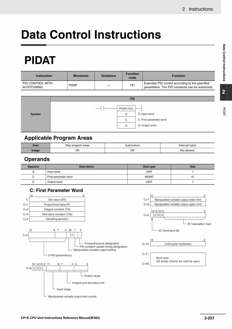
2 Instructions D
ata Co
ntro
l Instru
ction
s
2
PID
AT
Data Control Instructions
PIDAT
Applicable Program Areas
Operands
C: First Parameter Word
Instruction Mnemonic VariationsFunction
codeFunction
PID CONTROL WITH AUTOTUNING
PIDAT --- 191Executes PID control according to the specified parameters. The PID constants can be autotuned.
Symbol
PID
Area Step program areas Subroutines Interrupt tasks
Usage OK OK Not allowed
Operand Description Data type Size
S Input word UINT 1
C First parameter word WORD 41
D Output word UINT 1
S: Input word
C: First parameter word
D: Output word
PIDAT(191)
S
C
D
15 8 07
C+5 0
32 14
C
C+1
C+2
C+3
C+4
015
C+6
81112131415
0 0 0
0347
Set value (SV)
Proportional band (P)
Integral constant (Tik)
Derivative constant (Tdk)
Sampling period(τ)
Forward/reverse designationPID constant update timing designation
Manipulated variable output setting
Output range
Integral and derivative unit
Input range
Manipulated variable output limit control
2-PID parameter(α)
C+7
C+8
015
C+11
C+40
C+9
C+10015
015 1214130 0 0
Limit-cycle Hysteresis
Manipulated variable output lower limit
Manipulated variable output upper limit
Work area (30 words: Cannot be used by user.)
AT Calculation Gain
AT Command Bit
2-257CP1E CPU Unit Instructions Reference Manual(W483)

2 Instructions
Operand Specifications
Flags
FunctionWhen the execution condition is ON, PIDAT(191) carries out target value filtered PID control with twodegrees of freedom according to the parameters designated by C (set value, PID constant, etc.). Ittakes the specified input range of binary data from the contents of input word S and carries out the PIDaction according to the parameters that are set. The result is then stored as the manipulated variable inoutput word D.
The parameter settings are read when the execution condition turns from OFF to ON, and the ErrorFlag will turn ON if the settings are outside of the permissible range.If the settings are within the permissible range, PID processing will be executed using the initial values.Bumpless operation is not performed at this time. It will be used for manipulated variables in subse-quent PID processing execution. (Bumpless operation is processing that gradually and continuouslychanges the manipulated variable in order to avoid the adverse effects of sudden changes.)
When the execution condition turns ON, the PV for the specified sampling period is entered and pro-cessing is performed.
AutotuningThe status of the AT Command Bit (bit 15 of C+9) is checked every cycle. If this control bit is turned ONin a given cycle, PIDAT(191) will begin autotuning the PID constants. (The changes in the SV will not bereflected while autotuning is being performed.)The limit-cycle method is used for autotuning. PIDAT(191) forcibly changes the manipulated variable(max. manipulated variable ↔ min. manipulated variable) and monitors the characteristics of the con-trolled system. The PID constants are calculated based on the characteristics that were observed, andthe new P, I, and D constants are stored automatically in C+1, C+2, and C+3. At this point, the AT Com-mand Bit (bit 15 of C+9) is turned OFF and PID control resumes with the new PID constants in C+1,C+2, and C+3.
• If the AT Command Bit is ON when PIDAT(191) execution begins, autotuning will be performed firstand then PID control will start with the calculated PID constants.
• If the AT Command Bit is turned ON during PIDAT(191) execution, PIDAT(191) interrupts the PIDcontrol being performed with the user-set PID constants, performs autotuning, and then resumes PIDcontrol with the calculated PID constants.
Area Word addresses Indirect DM addresses
Constants CF Pulse bits TR bitsCIO WR HR AR T C DM @DM *DM
S, C, D OK OK OK OK OK OK OK OK OK --- --- --- ---
Name Label Operation
Error Flag P_ER • ON if the C data is out of range.
• ON if the actual sampling period is more than twice the designated sampling period.
• ON while it is recognized as an error if the manipulated variable does not change in 9999 seconds by limit-cycle during autotuning.
• OFF in all other cases.
Greater Than Flag P_GT • ON if the manipulated variable after the PID action exceeds the upper limit.
• OFF in all other cases.
Less Than Flag P_LT • ON if the manipulated variable after the PID action is below the lower limit.
• OFF in all other cases.
Carry Flag P_CY • ON while PID control is being executed.
• OFF in all other cases.
Parameters (C to C+8)
Manipulated variable (D)
PV input (S) PID control
2-258 CP1E CPU Unit Instructions Reference Manual(W483)

2 Instructions D
ata Co
ntro
l Instru
ction
s
2
PID
AT
The following flowchart shows the autotuning procedure:
Note 1 If autotuning is interrupted by turning OFF the AT Command Bit during autotuning, PID control will startwith the PID constants that were being used before autotuning began.
2 Also, if an AT execution error occurs, PID control will start with the PID constants that were being usedbefore autotuning began.
In both cases described in notes 1 and 2, the PID constants will be enabled if they were already calcu-lated when autotuning was interrupted.
PID Control• The number of valid input data bits within the 16 bits of the PV input (S) is designated by the input
range setting in C+6, bits 08 to 11. For example, if 12 bits (4 hex) is designated for the input range,the range from 0000 hex to 0FFF hex will be enabled as the PV. (Values greater than 0FFF hex willbe regarded as 0FFF hex.)
• The set value range also depends on the input range.
• Measured values (PV) and set values (SV) are in binary without sign, from 0000 hex to the maximumvalue of the input range.
• The number of valid output data bits within the 16 bits of the manipulated variable output is desig-nated by the output range setting in C+6, bits 00 to 03. For example, if 12 bits (4 hex) is designatedfor the output range, the range from 0000 hex to 0FFF hex will be output as the manipulated variable.
• For proportional operation only, the manipulated variable output when the PV equals the SV can bedesignated as follows:
0: Output 0%1: Output 50%.
• The direction of proportional operation can be designated as either forward or reverse.
• The upper and lower limits of the manipulated variable output can be designated.
• The sampling period can be designated in units of 10 ms (0.01 to 99.99 s), but the actual PID actionis determined by a combination of the sampling period and the time of PIDAT(191) instruction execu-tion (with each cycle).
• The timing of enabling changes made to PID constants can be set to either 1) the beginning ofPIDAT(191) instruction execution or 2) the beginning of PID instruction execution and each samplingperiod. Only the proportional band (P), integral constant (Tik), and derivative constant (Tdk) can bechanged each sampling cycle (i.e., during PID instruction execution). The timing is set in bit 1 of C+5.
• When the integral and derivative unit is designated as “1: Sampling period multiple”, and the integralconstant (Tik) is below 1 as a result of autotuning, the integral constant (Tik) will be 9999 (Integraloperation not executed). In the same way, when the integral and derivative unit is designated as “1:Sampling period multiple”, and the derivative constant (Tdk) is below 1 as a result of autotuning, thederivative constant (Tdk) will be 0 (Derivative operation not executed).
The AT Command Bit (bit 15 of C+9) is ON at the start of PIDAT(191) execution or it is turned ON during execution.
PID control is interrupted, the PV is forcibly changed, and the PID constants are calculated automatically.
The calculated P, I, and D constants are set in C+1, C+2, and C+3 respectively. The AT Command Bit is turned OFF.
PID control starts (or restarts) with the new PID constants.
2-259CP1E CPU Unit Instructions Reference Manual(W483)

2 Instructions
Hint• PIDAT(191) is executed as if the execution condition was a STOP-RUN signal. PID calculations are
executed when the execution condition remains ON for the next cycle after C+11 to C+40 are initial-ized. Therefore, when using the Always ON Flag (ON) as an execution condition for PIDAT(191), pro-vide a separate process where C+11 to C+40 are initialized when operation is started.
Precautions• A PID parameter storage word cannot be shared by multiple PIDAT instructions. Even when the same
parameter is used in multiple PIDAT instructions, separate words must be specified.
• When changing the PID constants manually, set the PID constant change enable setting (bit 1 ofC+5) to 1 so that the values in C+1, C+2, and C+3 are refreshed each sampling period in the PID cal-culation. This setting also allows the PID constants to be adjusted manually after autotuning.
• Of the PID parameters (C to C+40), only the following parameters can be changed when the execu-tion condition is ON. When any other values have been changed, be sure to change the executioncondition from OFF to ON to enable the new settings.
• Set value (SV) in C(Can be changed during PID control only. An SV change during autotuning will not bereflected.)
• PID constant change enable setting (bit 1 of C+5)
• P, I, and D constants in C+1, C+2, and C+3(Changes to these constants will be reflected each sampling period only if the PID constantchange enable setting (bit 1 of C+5) is set to 1.)
• AT Command Bit (bit 15 of C+9)
• AT Calculation Gain (bits 0 to 14 of C+9) and Limit-cycle Hysteresis (C+10) (These values areread when autotuning starts.)
Performance Specifications
Calculation MethodCalculations in PID control are performed by the target value filtered control with two degrees offreedom.
Item Specifications
PID control method --- Target value filter-type two-degrees-of-freedom PID method (forward/reverse)
Number of PID control loops --- Unlimited (1 loop per instruction)
Sampling period τ 0.01 to 99.99 s
PID constant Proportional band P 0.1 to 999.9%
Integral constant Tik 1 to 8191, 9999 (No integral action for sampling period multiple, 9999.)
Derivative constant Tdk 0 to 8191 (No derivative action for sampling period multiple, 0.)
Set value SV 0 to 65535 (Valid up to maximum value of input range.)
Measured value PV 0 to 65535 (Valid up to maximum value of input range.)
Manipulated variable MV 0 to 65535 (Valid up to maximum value of output range.)
2-260 CP1E CPU Unit Instructions Reference Manual(W483)

2 Instructions D
ata Co
ntro
l Instru
ction
s
2
PID
AT
Block Diagram for Target Value PID with Two Degrees of FreedomWhen overshooting is prevented with simple PID control, stabilization of disturbances is slowed (1). Ifstabilization of disturbances is speeded up, on the other hand, overshooting occurs and responsetoward the target value is slowed (2).
When target-value PID control with two degrees of freedom is used, on the other hand, there is noovershooting, and response toward the target value and stabilization of disturbances can both bespeeded up (3).
PID Parameter Settings
Control data Item Contents Setting rangeChange with ON input condition
C Set value (SV) The target value of the process being controlled. Binary data (of the same number of bits as specified for the input range)
Allowed
C+1 Proportional band The parameter for P action expressing the pro-portional control range/total control range.
0001 to 270F hex (1 to 9999);(0.1% to 999.9%, in units of 0.1%)
Can be changed with input condi-tion ON if bit 1 of C+5 is 1.
C+2 TikIntegral Constant
A constant expressing the strength of the integral action. As this value increases, the integral strength decreases.
0001 to 1FFF hex (1 to 8191);(9999 = Integral operation not executed) (See note 1.)
C+3 TdkDerivative Constant
A constant expressing the strength of the deriva-tive action. As this value increases, the derivative strength decreases.
0001 to 1FFF hex (1 to 8191);(0000 = Derivative operation not executed) (See note 1.)
C+4 Sampling period (τ) Sets the period for executing the PID action. 0001 to 270F hex (1 to 9999);(0.01 to 99.99 s, in units of 10 ms)
Not allowed
Bits 04 to 15 of C+5
2-PID parameter (α) The input filter coefficient. Normally use 0.65 (i.e., a setting of 000). The filter efficiency decreases as the coefficient approaches 0.
000 hex: α = 0.65Setting from 100 to 163 hex means that the value of the rightmost two digits is set from α= 0.00 to α= 0.99. (See note 2.)
Bit 03 of C+5 Manipulated variable output designation
Designates the manipulated variable output for when the PV equals the SV.
0: Output 0%1: Output 50%
Bit 01 of C+5 PID constant change enable setting
The timing of enabling changes made to the pro-portional band (P), integral constant (Tik), and derivative constant (Tdk) for use in PID calcula-tions.
0: At start of PID instruction execution1: At start of PID instruction execution and each sampling period
Allowed
1 + (1 – λ) Ti · s
1 + Ti · s
+
–
+
–
Kp +Kp
Ti · s
Kp Td/s
1 + λ · Td · s
(1)
(2)
(3)
Disturbance response
Simple PID Control Feed-forward PID Control
As the target response is slowed, the disturbance response worsens.
As the disturbance response is slowed, the target response worsens.
Overshoot
Target response
SV
PV
Kp:Proportional constantTi:Integral timeTd:Derivative times:Laplace operatorα:2-PID parameterλ:Incomplete derivative coefficient
Measured value (PV)
Set value (target value)
Target value filter Proportional + integral elements
Preceding derivative-type elements
Manipulated variable
2-261CP1E CPU Unit Instructions Reference Manual(W483)

2 Instructions
Note 1 When the unit is designated as 1, the range is from 1 to 8,191 times the period. When the unit is designated as 9, therange is from 0.1 to 819.1 s. When 9 is designated, set the integral and derivative times to within a range of 1 to 8,191times the sampling period.
2 Setting the 2-PID parameter (α) to 000 yields 0.65, the normal value.
3 When the manipulated variable output limit control is enabled (i.e., set to “1”), set the values as follows:0000 ≤ MV output lower limit ≤ MV output upper limit ≤ Max. value of output range
Bit 00 of C+5 PID forward/reverse designation
Determines the direction of the proportional action.
0: Reverse action
1: Forward action
Not allowed
Bit 12 of C+6 Manipulated variable output limit control
Determines whether or not limit control will apply to the manipulated variable output.
0: Disabled (no limit control)1: Enabled (limit control)
Bits 08 to 11 of C+6
Input range The number of input data bits. 0: 8 bits 5: 13 bits1: 9 bits 6: 14 bits2: 10 bits 7: 15 bits3: 11 bits 8: 16 bits4: 12 bits
Bits 04 to 07 of C+6
Integral and deriva-tive unit
Determines the unit for expressing the integral and derivative constants.
1: Sampling period multiple9: Time (unit: 100 ms)
Bits 00 to 03 of C+6
Output range The number of output data bits. (The number of output bits is automatically the same as the num-ber of input bits.)
0: 8 bits 5: 13 bits1: 9 bits 6: 14 bits2: 10 bits 7: 15 bits3: 11 bits 8: 16 bits4: 12 bits
C+7 Manipulated variable output lower limit
The lower limit for when the manipulated variable output limit is enabled.
0000 to FFFF (binary)(See note 3.)
C+8 Manipulated variable output upper limit
The upper limit for when the manipulated variable output limit is enabled.
0000 to FFFF (binary)(See note 3.)
Bit 15 of C+9 AT Command Bit This control bit starts autotuning.
• Set the AT Command Bit to 1 to perform auto-tuning. (Autotuning can be started while PIDAT(191) is being executed.)
• This bit is turned OFF automatically when auto-tuning is completed.
If autotuning is interrupted by turning OFF the AT Command Bit during autotuning, PID control will start with the PID constants that were being used before autotuning began. But if the PID constants were changed after autotuning began, PID control will start with the value set at the time autotuning was interrupted.
As a Control Bit:
• 0 → 1:Executes autotuning.
• 1 → 0:
Interrupts autotuning.(PID(191) turns the bit OFF automatically when autotuning is completed.
As a Flag:0: Autotuning is not being executed.1: Autotuning is being executed.
Allowed
Bits 00 to 11 of C+9
AT Calculation Gain Set this parameter to adjust the contribution of the PID calculation results to the stored values.Normally, leave this parameter set to its default (0000).
• Increase the value when emphasizing stability.
• Decrease the value when emphasizing respon-siveness.
0000 hex: 1.00 (Default)0001 to 03E8 hex (1 to 1000);(0.01 to 10.00, in units of 0.01)
Allowed(These parameters are read when autotuning starts.)
C+10 Limit-cycle Hysteresis Sets the hysteresis when the limit cycle is gener-ated. The default setting for reverse operation turns ON the MV with a hysteresis of SV−20%.Increase this setting if a proper limit cycle cannot be generated because the PV is unstable. How-ever, the AT accuracy will decline if the Limit-cycle Hysteresis is higher than necessary.
0000 hex: 0.20% (Default)0001 to 03E8 hex: 0.01 to 10.00% in units of 0.01%FFFF hex: 0.00%
Note The percentage is with respect to theinput range.
Control data Item Contents Setting rangeChange with ON input condition
2-262 CP1E CPU Unit Instructions Reference Manual(W483)

2 Instructions D
ata Co
ntro
l Instru
ction
s
2
PID
AT
Sampling Period and Cycle TimeThe sampling period can be designated in units of 10 ms (0.01 to 99.99 s), but the actual PID action isdetermined by a combination of the sampling period and the time of PID instruction execution (witheach cycle). The relationship between the sampling period and the cycle time is as follows:
• If the sampling period is less than the cycle time, PID control is executed with each cycle and not witheach sampling period.
• If the sampling period is greater than or equal to the cycle time, PID control is not executed with eachcycle, but PID(190) is executed when the cumulative value of the cycle time (the time between PIDinstructions) is greater than or equal to the sampling period. The surplus portion of the cumulativevalue (i.e., the cycle time’s cumulative value minus the sampling period) is carried forward to the nextcumulative value.
For example, suppose that the sampling period is 100 ms and that the cycle time is consistently 60ms. For the first cycle after the initial execution, PID(190) will not be executed because 60 ms is lessthan 100 ms. For the second cycle, 60 ms + 60 ms is greater than 100 ms, so PID(190) will beexecuted. The surplus of 20 ms (i.e., 120 ms – 100 ms = 20 ms) will be carried forward.
For the third cycle, the surplus 20 ms is added to 60 ms. Because the sum of 80 ms is less than 100ms, PID(190) will not be executed. For the fourth cycle, the 80 ms is added to 60 ms. Because thesum of 140 ms is greater than 100 ms, PID(190) will be executed and the surplus of 40 ms (i.e.,120 ms – 100 ms = 20 ms) will be carried forward. This procedure is repeated for subsequent cycles.
1 cycle 1 cycle 1 cycle 1 cycle 1 cycle
ProcessingInitial processing (60 ms) (60 ms + 60 ms = 120 ms) (20 ms + 60 ms = 80 ms)
(80 ms + 60 ms = 140 ms)
(PID processing with initial values)
Reading of measurement time
Less than 100 ms, so PID is not executed.
Greater than 100 ms, so PID is executed and 20 ms is carried forward.
Less than 100 ms, so PID is not executed.
Not executed. Executed Not executed. Executed
Greater than 100 ms, so PID is executed and 40 ms is carried forward.
60ms
PID
60ms
PID
60ms
PID
60ms
PID PID
2-263CP1E CPU Unit Instructions Reference Manual(W483)

2 Instructions
PID control Proportional Action (P)
Proportional action is an operation in which a proportional band is established with respect to the setvalue (SV), and within that band the manipulated variable (MV) is made proportional to the deviation.An example for reverse operation is shown in the following illustration.
If the proportional action is used and the present value (PV) becomes smaller than the proportionalband, the manipulated variable (MV) is 100% (i.e., the maximum value). Within the proportional band,the MV is made proportional to the deviation (the difference between from SV and PV) and graduallydecreased until the SV and PV match (i.e., until the deviation is 0), at which time the MV will be at theminimum value of 0% (or 50%, depending on the setting of the manipulated variable output designationparameter). The MV will also be 0% when the PV is larger than the SV.
The proportional band is expressed as a percentage of the total input range. The smaller the propor-tional band, the larger the proportional constant and the stronger the corrective action will be. With pro-portional action an offset (residual deviation) generally occurs, but the offset can be reduced by makingthe proportional band smaller. If it is made too small, however, hunting will occur.
Integral Action (I)Combining integral action with proportional action reduces the offset according to the time that haspassed, so that the PV will match the SV. The strength of the integral action is indicated by the integraltime, which is the time required for the manipulated variable of the integral action to reach the samelevel as the manipulated variable of the proportional action with respect to the step deviation, as shownin the following illustration. The shorter the integral time, the stronger the correction by the integralaction will be. If the integral time is too short, the correction will be too strong and will cause hunting tooccur.
SV
Adjusting the Proportional BandProportional Action (Reverse Action)
Proportional band too narrow (hunting occurring)
Offset
Proportional band just right
Proportional band too wide (large offset)
100%
50%
0%
Manipulated variable
Set point
Proportional band when MV output designation is 0 (output 0%)
Proportional band when MV output designation is 1 (output 50%)
Proportional band when MV output designation is 1 (output 50%)
Proportional band when MV output designation is 0 (output 0%)
0
0
PI action
P action
Step response
I action
Integral Action
Step response
Ti: Integral time
Manipulated variable
Deviation
Manipulated variable
Deviation
Pi Action and Integral Time
0
0Ti
2-264 CP1E CPU Unit Instructions Reference Manual(W483)
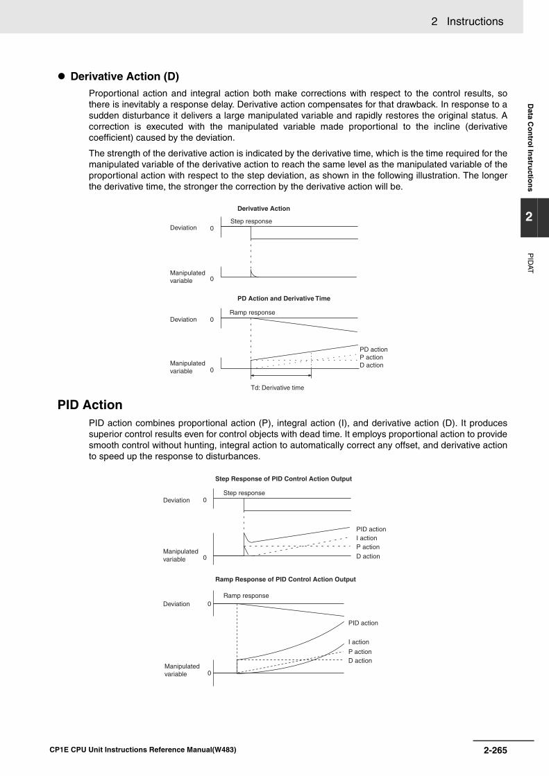
2 Instructions D
ata Co
ntro
l Instru
ction
s
2
PID
AT
Derivative Action (D)Proportional action and integral action both make corrections with respect to the control results, sothere is inevitably a response delay. Derivative action compensates for that drawback. In response to asudden disturbance it delivers a large manipulated variable and rapidly restores the original status. Acorrection is executed with the manipulated variable made proportional to the incline (derivativecoefficient) caused by the deviation.
The strength of the derivative action is indicated by the derivative time, which is the time required for themanipulated variable of the derivative action to reach the same level as the manipulated variable of theproportional action with respect to the step deviation, as shown in the following illustration. The longerthe derivative time, the stronger the correction by the derivative action will be.
PID ActionPID action combines proportional action (P), integral action (I), and derivative action (D). It producessuperior control results even for control objects with dead time. It employs proportional action to providesmooth control without hunting, integral action to automatically correct any offset, and derivative actionto speed up the response to disturbances.
0
0
0
0
Ramp response
Step response
PD action P action D action
Td: Derivative time
Manipulated variable
Deviation
Manipulated variable
Deviation
Derivative Action
PD Action and Derivative Time
0
0
0
0
PID actionI actionP action
D action
Step response
PID action
I action
P actionD action
Ramp response
Manipulated variable
Manipulated variable
Step Response of PID Control Action Output
Ramp Response of PID Control Action Output
Deviation
Deviation
2-265CP1E CPU Unit Instructions Reference Manual(W483)

2 Instructions
Direction of ActionWhen using PID control, select either of the following two control directions. In either direction, the MVincreases as the difference between the SV and the PV increases.
• Forward action: MV is increased when the PV is larger than the SV.
• Reverse action: MV is increased when the PV is smaller than the SV.
Adjusting PID ParametersThe general relationship between PID parameters and control status is shown below.
• When it is not a problem if a certain amountof time is required for stabilization (settle-ment time), but it is important not to causeovershooting, then enlarge the proportionalband.
• When overshooting is not a problem but it isdesirable to quickly stabilize control, thennarrow the proportional band. If the propor-tional band is narrowed too much, however,then hunting may occur.
• When there is broad hunting, or when oper-ation is tied up by overshooting and under-shooting, it is probably because integralaction is too strong. The hunting will bereduced if the integral time is increased orthe proportional band is enlarged.
• If the period is short and hunting occurs, itmay be that the control system response isquick and the derivative action is too strong.In that case, set the derivative action lower.
100%
50%
0%
100%
50%
0%
Output Output
Forward ActionReverse Action
Low temperature
SV SVHigh temperature
Low temperature
High temperature
(MV output designation: 50%)
SV
Control by measured PID
When P is enlarged
SV
When P is narrowed
Control by measured PID
SV
Control by measured PID (when loose hunting occurs)
Enlarge I or P.
SV
Control by measured PID (when hunting occurs in a short period)
Lower D.
2-266 CP1E CPU Unit Instructions Reference Manual(W483)
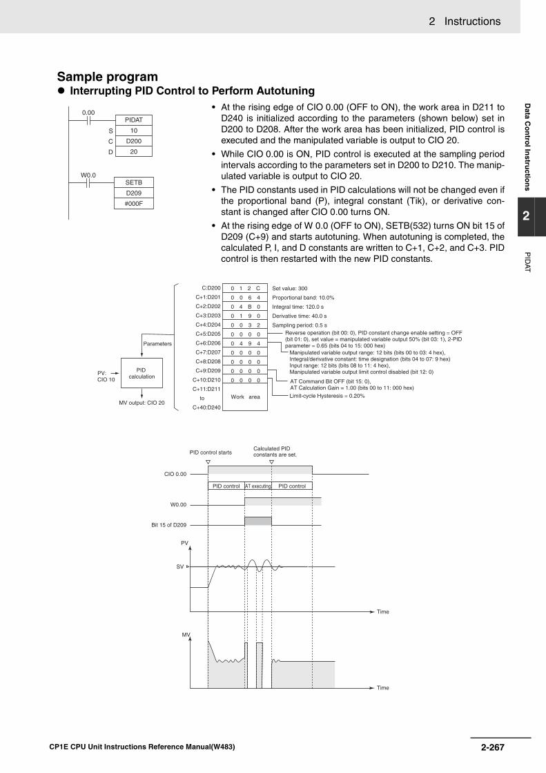
2 Instructions D
ata Co
ntro
l Instru
ction
s
2
PID
AT
Sample program Interrupting PID Control to Perform Autotuning
• At the rising edge of CIO 0.00 (OFF to ON), the work area in D211 toD240 is initialized according to the parameters (shown below) set inD200 to D208. After the work area has been initialized, PID control isexecuted and the manipulated variable is output to CIO 20.
• While CIO 0.00 is ON, PID control is executed at the sampling periodintervals according to the parameters set in D200 to D210. The manip-ulated variable is output to CIO 20.
• The PID constants used in PID calculations will not be changed even ifthe proportional band (P), integral constant (Tik), or derivative con-stant is changed after CIO 0.00 turns ON.
• At the rising edge of W 0.0 (OFF to ON), SETB(532) turns ON bit 15 ofD209 (C+9) and starts autotuning. When autotuning is completed, thecalculated P, I, and D constants are written to C+1, C+2, and C+3. PIDcontrol is then restarted with the new PID constants.
PIDAT
10
D200
20
0.00
S
C
D
W0.0SETB
D209
#000F
C:D200
C+1:D201
C+2:D202
C+3:D203
C+4:D204
C+5:D205
C+6:D206
C+7:D207
C+8:D208
C+9:D209
C+10:D210
C+11:D211
C+40:D240
Set value: 300
Proportional band: 10.0%
Integral time: 120.0 s
Derivative time: 40.0 s
Sampling period: 0.5 s
PID calculation
Parameters
PV: CIO 10
MV output: CIO 20
Reverse operation (bit 00: 0), PID constant change enable setting = OFF (bit 01: 0), set value = manipulated variable output 50% (bit 03: 1), 2-PID parameter = 0.65 (bits 04 to 15: 000 hex)
AT Command Bit OFF (bit 15: 0), AT Calculation Gain = 1.00 (bits 00 to 11: 000 hex)
CIO 0.00
PID control startsCalculated PID constants are set.
W0.00
Bit 15 of D209
PV
SV
Time
MV
Time
to
0 1 2 C
0 0 6 4
0 4 B 0
0 1 9 0
0 0 3 2
0 0 0 0
0 4 9 4
0 0 0 0
0 0 0 0
0 0 0 0
0 0 0 0
Work area
Manipulated variable output range: 12 bits (bits 00 to 03: 4 hex),Integral/derivative constant: time designation (bits 04 to 07: 9 hex)Input range: 12 bits (bits 08 to 11: 4 hex),Manipulated variable output limit control disabled (bit 12: 0)
Limit-cycle Hysteresis = 0.20%
PID control PID controlAT executing
2-267CP1E CPU Unit Instructions Reference Manual(W483)

2 Instructions
Starting PIDAT(191) with Autotuning
Interrupting Autotuning Before CompletionAutotuning can be interrupted by turning bit 15 of D209 (C+9) from ON to OFF. PID control will berestarted with the P, I, and D constants that were in effect before autotuning was started.
At the rising edge of CIO 0.00 (OFF to ON), autotuning will be performed first if bit15 of D209 (C+9) is ON. When autotuning is completed, the calculated P, I, and Dconstants are written to C+1, C+2, and C+3. PID control is then started with thecalculated PID constants.
PIDAT
10
D200
20
0.00
S
C
D
CIO 0.00
PV
SV
MV
PID control and autotuning start.
Calculated PID constants are set.
AT executing PID control
Bit 15 of D209
Time
Time
CIO 0.00
PV
SV
PID control starts.
PID control AT executing PID control
AT starts AT is interrupted.
Bit 15 of D209
PID control is restarted with the existing PID constants.
Time
2-268 CP1E CPU Unit Instructions Reference Manual(W483)
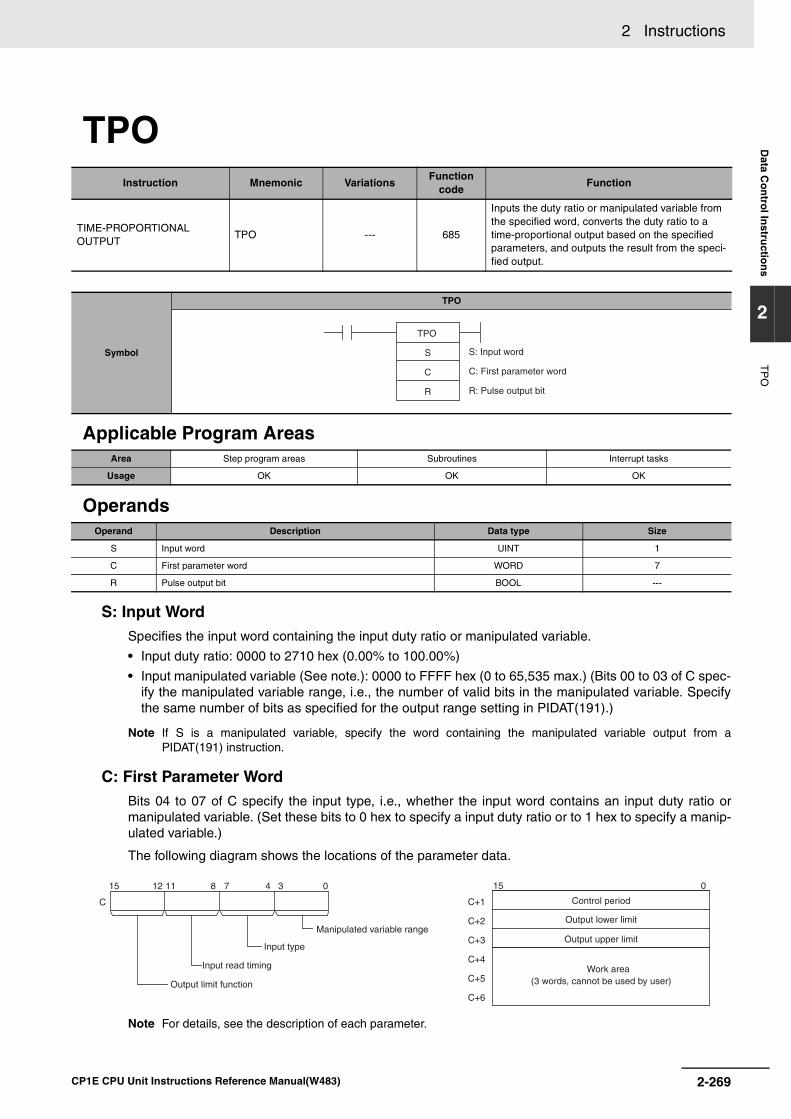
2 Instructions D
ata Co
ntro
l Instru
ction
s
2
TP
O
TPO
Applicable Program Areas
Operands
S: Input WordSpecifies the input word containing the input duty ratio or manipulated variable.
• Input duty ratio: 0000 to 2710 hex (0.00% to 100.00%)
• Input manipulated variable (See note.): 0000 to FFFF hex (0 to 65,535 max.) (Bits 00 to 03 of C spec-ify the manipulated variable range, i.e., the number of valid bits in the manipulated variable. Specifythe same number of bits as specified for the output range setting in PIDAT(191).)
Note If S is a manipulated variable, specify the word containing the manipulated variable output from aPIDAT(191) instruction.
C: First Parameter WordBits 04 to 07 of C specify the input type, i.e., whether the input word contains an input duty ratio ormanipulated variable. (Set these bits to 0 hex to specify a input duty ratio or to 1 hex to specify a manip-ulated variable.)
The following diagram shows the locations of the parameter data.
Note For details, see the description of each parameter.
Instruction Mnemonic VariationsFunction
codeFunction
TIME-PROPORTIONAL OUTPUT
TPO --- 685
Inputs the duty ratio or manipulated variable from the specified word, converts the duty ratio to a time-proportional output based on the specified parameters, and outputs the result from the speci-fied output.
Symbol
TPO
Area Step program areas Subroutines Interrupt tasks
Usage OK OK OK
Operand Description Data type Size
S Input word UINT 1
C First parameter word WORD 7
R Pulse output bit BOOL ---
S: Input word
C: First parameter word
R: Pulse output bit
TPO
S
C
R
C+1
C+2
C+3
C+4
C+5
C+6
015
C
815 12 11 0347
Manipulated variable range
Input type
Input read timing
Output limit function
Control period
Output lower limit
Output upper limit
Work area(3 words, cannot be used by user)
2-269CP1E CPU Unit Instructions Reference Manual(W483)
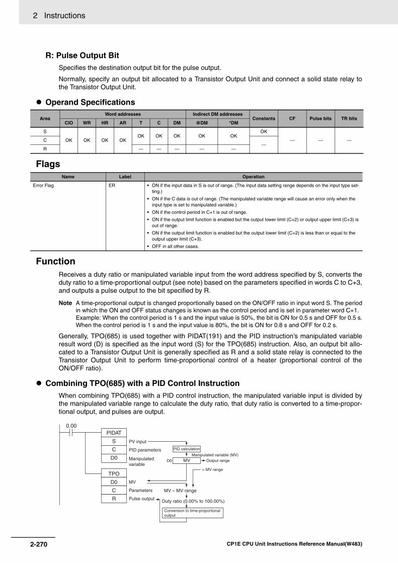
2 Instructions
R: Pulse Output BitSpecifies the destination output bit for the pulse output.
Normally, specify an output bit allocated to a Transistor Output Unit and connect a solid state relay tothe Transistor Output Unit.
Operand Specifications
Flags
FunctionReceives a duty ratio or manipulated variable input from the word address specified by S, converts theduty ratio to a time-proportional output (see note) based on the parameters specified in words C to C+3,and outputs a pulse output to the bit specified by R.
Note A time-proportional output is changed proportionally based on the ON/OFF ratio in input word S. The periodin which the ON and OFF status changes is known as the control period and is set in parameter word C+1.Example: When the control period is 1 s and the input value is 50%, the bit is ON for 0.5 s and OFF for 0.5 s.When the control period is 1 s and the input value is 80%, the bit is ON for 0.8 s and OFF for 0.2 s.
Generally, TPO(685) is used together with PIDAT(191) and the PID instruction’s manipulated variableresult word (D) is specified as the input word (S) for the TPO(685) instruction. Also, an output bit allo-cated to a Transistor Output Unit is generally specified as R and a solid state relay is connected to theTransistor Output Unit to perform time-proportional control of a heater (proportional control of theON/OFF ratio).
Combining TPO(685) with a PID Control InstructionWhen combining TPO(685) with a PID control instruction, the manipulated variable input is divided bythe manipulated variable range to calculate the duty ratio, that duty ratio is converted to a time-propor-tional output, and pulses are output.
Area Word addresses Indirect DM addresses
Constants CF Pulse bits TR bitsCIO WR HR AR T C DM @DM *DM
S
OK OK OK OKOK OK OK OK OK
OK
--- --- ---C---
R --- --- --- --- ---
Name Label Operation
Error Flag ER • ON if the input data in S is out of range. (The input data setting range depends on the input type set-ting.)
• ON if the C data is out of range. (The manipulated variable range will cause an error only when the input type is set to manipulated variable.)
• ON if the control period in C+1 is out of range.
• ON if the output limit function is enabled but the output lower limit (C+2) or output upper limit (C+3) is out of range.
• ON if the output limit function is enabled but the output lower limit (C+2) is less than or equal to the output upper limit (C+3).
• OFF in all other cases.
0.00PIDAT
S
C
D0
TPO
D0
C
R
MVD0
PV input
PID parameters
MV
Parameters
Pulse output
Manipulated variable (MV)Output range
= MV range
MV ÷ MV range
Duty ratio (0.00% to 100.00%)
Manipulated variable
PID calculation
Conversion to time-proportional output
2-270 CP1E CPU Unit Instructions Reference Manual(W483)

2 Instructions D
ata Co
ntro
l Instru
ction
s
2
TP
O
In this case, set the same value for the PID Control instruction’s output range and the TPO(685) instruc-tion’s manipulated variable range. For example, when the PID Control instruction’s output range and theTPO(685) instruction’s manipulated variable range are both set to 12 bits (0000 to 0FFF hex), the dutyratio is calculated by dividing the manipulated variable from the PID Control instruction by 0FFF hexand TPO(685) converts that duty ratio to a time-proportional output.
External Wiring ExampleConnect the Transistor Output Unit to a solid state relay (SSR) as shown in the following diagram.
Parameter Settings
Note When the output limit control function is enabled, set the lower and upper limits as follows: 0000 hex ≤ lower limit ≤ upper limit ≤ 2710 hex.
Execution• The instruction is executed while the input condition is ON.
• When instruction execution starts, the output bit (R) is turned ON/OFF according to the duty ratio.
Control dataItem Contents Setting range
Change with ON input conditionWord Bits
C 00 to 03 Manipulated variable range
Specifies the number of input data bits. 0 hex: 8 bits 5 hex: 13 bits1 hex: 9 bits 6 hex: 14 bits2 hex: 10 bits 7 hex: 15 bits3 hex: 11 bits 8 hex: 16 bits4 hex: 12 bits
Allowed
04 to 07 Input type Specifies whether S contains a duty ratio or manipulated variable.
0 hex: Duty ratioSetting range for S: 0000 to 2710 hex (0.00 to 100.00%)
1 hex: Manipulated variableSetting range for S: 0000 to FFFF hex (0 to 65,535)(The maximum setting depends on the MV range set with bits 00 to 03 of C.)
Allowed
08 to 11 Input read tim-ing
Specifies the input read timing. 0 hex: Use the beginning value of the control period
1 hex: Use lower value
2 hex: Use higher value
3 hex: Continuous adjustment
Allowed
12 to 15 Output limit control
Specifies whether the output limit function is enabled or disabled.
0 hex: Disabled
1 hex: Enabled (See note.)
Allowed
C+1 00 to 15 Control period Control period(Time period in which the ON/OFF changes are made.)
0064 to 270F hex (1.00 to 99.99 s)
Note For example, 1.00 s is set as 0064 hex, and not0001 hex.
Allowed
C +2 00 to 15 Output lower limit
Specifies the lower limit when the output limit is enabled.
0000 to 2710 hex (0 to 100.00%) Allowed
C +3 00 to 15 Output upper limit
Specifies the upper limit when the output limit is enabled.
0000 to 2710 hex (0 to 100.00%) Allowed
C+4 00 to 15 Work area This work area is used by the system. It cannot be used by the user.
Cannot be used. ---
C+5 00 to 15
C+6 00 to 15
COM
SSR
AC
+
Transistor Output UnitHeater
12 to 24 VDC
2-271CP1E CPU Unit Instructions Reference Manual(W483)

2 Instructions
• The parameters (in C to C+3) are read in real time each time that the instruction is executed. Whenchanging the parameters, change all of them at the same time so that different sets of parameters arenot mixed.
• The output (R) is turned ON/OFF when the instruction is executed and the accuracy of the output’sON/OFF timing is 10 ms max.
• Execution of the instruction stops when the input condition goes OFF. At that time, the elapsed timevalue will be reset and the control period will be initialized.
• The input type setting (bits 04 to 07 of C) determines whether the input word (S) contains a duty ratioor manipulated variable. When S contains the manipulated variable, the duty ratio is calculated bydividing the manipulated variable input by the manipulated variable range (bits 00 to 03 of C).
• The input read timing setting (bits 08 to 11 of C) specifies when the input word (S) is read, as shownin the following table:
The following diagrams show the operation of each input read timing setting.
• Input time setting = 0 (Use the beginning value of the control period.)
• Input time setting = 1 (Use lower value.)
Input read timing Description
0: Use the beginning value of the control period
The duty ratio input is read at the beginning of the control period and the ratio cannot be changed during the control period.
1: Use lower value If the duty ratio input falls below the duty ratio at the beginning of the control period, the lower value will take precedence and the output ON time will be reduced accordingly.
2: Use higher value If the duty ratio input rises above the duty ratio at the beginning of the control period, the higher value will take precedence and the output ON time will be increased accordingly.
3: Continuous adjustment The duty ratio will be read in real time each time the instruction is executed and the ON/OFF operation will be repeated within the control period.
100%
a × 0.55 s a × 0.45 s a × 0.70 s a × 0.30 s
70%55%
0%
Control period (a)
Read only at the beginning of the control period.
Control period (a)
Time
Output
Duty ratio (MV/MV range)
Each control period’s output is determined by the duty ratio at the beginning of that period.Use this setting for general applications.
100%
a × 0.35 s a × 0.65 s a × 0.70 s a × 0.30 s
70%55%
35%
0%
Control period (a) Control period (a)
Time
Output
Duty ratio(MV/MV range)
55% target cut to 35%.
70% target is kept.
If the duty ratio falls below the initial value early enough, the duty ratio will be adjusted and the output will be turned OFF sooner.Use this setting for applications such as avoiding overshooting when using time-proportional control to control heating and using a relatively long control period.
2-272 CP1E CPU Unit Instructions Reference Manual(W483)

2 Instructions D
ata Co
ntro
l Instru
ction
s
2
TP
O
• Input time setting = 2 (Use higher value.)
• Input time setting = 3 (Continuous adjustment)
• The output limiter function (bits 12 to 15 of C) can be enabled to restrict (saturate) output when it isoutside the range between the output limiter lower limit (C + 2) and output limiter upper limit (C + 3).
100%
a × 0.45 s a × 0.55 s a × 0.80 s
80%70%55%
0%
a ×0.20 s
If the duty ratio rises above the initial value early enough, the duty ratio will be adjusted and the output will be turned ON sooner. (With this setting the output’s ON/OFF order is reversed and the output goes from OFF to ON.)Use this setting for applications such as avoiding undershooting when using time-proportional control to control cooling and using relatively long control period.
70% target is kept.
Control period (a) Control period (a)
Time
Output
Duty ratio(MV/MV range)
70% target raised to 80%.
100%
100%
a × 0.35 s
0%a ×0.20 s
a × 0.20 s
a × 0.20 s
Changes in the duty ratio are monitored in real time. If the duty ratio falls below the initial value early enough, the duty ratio will be adjusted and the output will be turned OFF sooner. If the duty ratio rises again after that, the ratio will be adjusted again and the output will be turned ON. This process is repeated continuously.Use this setting to improve responsiveness when the control period is relatively long and the duty ratio changes quickly. This setting is also appropriate for lighting or power applications that require precise control.
Control period (a)Control period (a)
Output
Duty ratio(MV/MV range)
: Output ON
: Output OFF
Time
2-273CP1E CPU Unit Instructions Reference Manual(W483)

2 Instructions
PrecautionsWhen using TPO(685) in combination with PIDAT(191) in a cyclic task and also using an interrupttask, temporarily disable interrupts by executing DI(693) (DISABLE INTERRUPTS) ahead PIDAT(191)and TPO(685). If interrupts are not disabled and an interrupt occurs between the PIDAT(191) andTPO(685), the control period may be shifted.
Sample program Combining TPO(685) with PIDAT(191)
When CIO 0.00 is ON, TPO(685) takes the manipulated variable output from PIDAT(191) (contained inD0), calculates the duty ratio from that manipulated variable value (Duty ratio = MV ÷ MV range), con-verts the duty ratio to a time-proportional output, and outputs the pulses to bit 01 of CIO 100.
In this case, CIO 100 is allocated to a Transistor Output Unit and bit CIO 100.01 is connected to a solidstate relay for heater control.
DI
EI
S
C
D
S
C
R
Reception prohibited
Reception allowed
Interrupt task
Interrupt task
Cyclic task
PIDAT
PV input
PID parameters
Parameters
TPO
Pulse output
Manipulated variable
Manipulated variable
0.00PIDAT
10
D200
D0
TPO
D0
D500
100.01
S
C
D
D200
D201
:
D206
:
:
D500
S
C
R
4
41
PV input
PID parameters
Manipulated variable
Manipulated variable
Parameters
Pulse output
Set value (SV)
Proportional band (P)
Output range: 4 hex
(12 bits: 0000 to 0FFF hex)
MV range: 4 hex
(12 bits: 0000 to 0FFF hex)
Input type: 1 hex (MV)
When CIO 0.00 goes from OFF to ON, PID(190) reads the parameters, performs the PID calculation with the PV input in CIO 10, and outputs the manipulated variable (MV) to D0.
TPO(685) calculates the duty ratio by dividing the MV in D0 by the MV range (0FFF Hex since the range is set to 12 bits), converts that duty ratio to a time-proportional output, and outputs the pulse output to bit 01 of CIO 100.
2-274 CP1E CPU Unit Instructions Reference Manual(W483)

2 Instructions D
ata Co
ntro
l Instru
ction
s
2
TP
O
Using TPO(685) AloneWhen CIO 0.00 is ON, TPO(685) takes the duty ratio in D10, converts the duty ratio to a time-propor-tional output, and outputs the pulses to bit 00 of CIO 100.
In this case, the control period is 1 s and the output limit function is enabled with a lower limit 20.00%and an upper limit of 80.00%.
0.00TPO
D10
D0
100.00
S
C
R
D0
D1
D2
D3
D4
D5
D6
:
:
D10
0
4
0
0
0
6
D
4
1
0
7
F
1
0
0
1
Duty ratio
Parameters
Pulse output
Duty ratio input, read initial value, and enable output limit function.
Control period = 1.00 s
Output lower limit = 20.00%
Output upper limit = 80.00%
0 to 100.00%
Do not set.
Do not set.
Do not set.
0 to 2710 hex
TPO(685) takes the duty ratio in D10, converts that duty ratio to a time-proportional output, and outputs the pulse output to bit 00 of CIO 100.
2-275CP1E CPU Unit Instructions Reference Manual(W483)

2 Instructions
SCL
Applicable Program Areas
Operands
P1: First Parameter Word
Operand Specifications
Instruction Mnemonic VariationsFunction
codeFunction
SCALING SCL @SCL 194Converts unsigned binary data into unsigned BCD data according to the specified linear function.
Symbol
SCL
Area Step program areas Subroutines Interrupt tasks
Usage OK OK OK
Operand Description Data type Size
S Source word UINT 1
P1 First parameter word LWORD 4
R Result word WORD 1
Note P1 to P1+3 must be in the same area.
Area Word addresses Indirect DM addresses
Constants CF Pulse bits TR bitsCIO WR HR AR T C DM @DM *DM
S, P1, R OK OK OK OK OK OK OK OK OK --- --- --- ---
S: Source word
P1: First parameter word
R: Result word
SCL(194)
S
P1
R
P1
P1+1
P1+2
P1+3
15 0
15 0
15 0
15 0
Scaled value for point A (Ar) 0000 to 9999 (4-digit BCD)
Unscaled value for point A (As) 0000 to FFFF (binary)
Scaled value for point B (Br) 0000 to 9999 (4-digit BCD)
Unscaled value for point B (Bs) 0000 to FFFF (binary)
2-276 CP1E CPU Unit Instructions Reference Manual(W483)

2 Instructions D
ata Co
ntro
l Instru
ction
s
2
SC
L
Flags
FunctionSCL(194) is used to convert the unsigned binary data contained in the source word S into unsignedBCD data and place the result in the result word R according to the linear function defined by points(As, Ar) and (Bs, Br). The address of the first word containing the coordinates of points (As, Ar) and (Bs,Br) is specified for the first parameter word P1. These points define by 2 values (As and Bs) before scal-ing and 2 values (Ar and Br) after scaling.
The following equations are used for the conversion.
Points A and B can define a line with either a positive or negative slope. Using a negative slope enablesreverse scaling.
• The result will be rounded to the nearest integer. If the result is less than 0000, 0000 will be output asthe result.
• If the result is greater than 9999, 9999 will be output.
Hint• SCL(194) can be used to scale the results of analog signal conversion values from Analog Input
Units according to user-defined scale parameters. For example, if a 1 to 5-V input to an Analog InputUnit is input to memory as 0000 to 0FA0 hexadecimal, the value in memory can be scaled to 50 to200°C using SCL(194).
• SCL(194) converts unsigned binary to unsigned BCD. To convert a negative value, it will be neces-sary to first add the maximum negative value in the program before using SCL(194) (see example).SCL(194) cannot output a negative value to the result word, R. If the result is a negative value, 0000will be output to R.
Name Label Operation
Error Flag P_ER • ON if the contents of P1 (Ar) or P1+1 (Br) is not BCD.
• ON if the contents of P1+1 (As) and P1+3 (Bs) are equal.
• OFF in all other cases.
Equals Flag P_EQ • ON if the result is 0.
• OFF in all other cases.
× BCD conversion of (Bs – S) (Br – Ar)
R = Bd –BCD conversion of (Bs – As)
P
P1+1
P1+2
P1+3
R (unsigned BCD)
Converted value
Converted value
S (unsigned binary)
Point B
Point A
Ar(BCD)
As(BIN)
Br(BCD)
Bs(BIN)
As
Br
Ar
Bs
Scaling is performed according to the linear function defined by points A and B.
2-277CP1E CPU Unit Instructions Reference Manual(W483)

2 Instructions
Sample programIn the following example, it is assume that an analog signal from 1 to 5 V is converted and input to D0as 0000 to 0FA0 hexadecimal. SCL(194) is used to convert (scale) the value in CIO 200 to a valuebetween 0 and 300 BCD.
When CIO 0.00 is ON, the contents of D0 is scaled using the linear function defined by point A (0000,0000) and point B (0FA0, 0300). The coordinates of these points are contained in D100 to D103, andthe result is output to D200.
Reference:An Analog Input Unit actually inputs values from FF38 to 1068 hexadecimal for 0.8 to 5.2 V. SCL(194),however, can handle only unsigned binary values between 0000 and FFFF hexadecimal, making itimpossible to use SCL(194) directly to handle signed binary values below 1 V (0000 hexadecimal), i.e.,FF38 to FFFF hexadecimal. In an actual application, it is thus necessary to add 00C8 hexadecimal toall values so that FF38 hexadecimal is represented as 0000 hexadecimal before using SCL(194), asshown in the following example.
Contents of D200 (R)
Contents of D0 (S)
Point B
Point A
SCL
D0
D100
D200
0.00 S
P1
R
P1: D100
P1+1:D101
P1+2:D102
P1+3:D103
Ar(BCD)
As(BIN)
Br(BCD)
Bs(BIN)
0300
00000000Hex
1V
0FA0Hex
5V
0 0 0 0
0 0 0 0
0 3 0 0
0 F A 0
+
200
#000C8
D0
SCL
D0
D100
D200
5.2V5V
1V0.8V
1068 Hex0FA0 Hex
0000 HexFF38 Hex
1130Hex1068Hex
00C8Hex0000Hex
+00C8 Hex
The value in CIO 0200 plus 00C8 hexadecimal
P1: D100
P1+1:D101
P1+2:D102
P1+3:D103
Ar(BCD)
As(BIN)
Br(BCD)
Bs(BIN)
0000Hex
0.8V
0300
0000
0315
1068Hex
5V
00C8Hex
1V
1130Hex
5.2V
Contents of D 200 (R)
Point B
Point AContents of D0 (S)
Point A (00C8 Hex → 0000 (BCD))Point B (1068 Hex → 0300 (BCD))
0 0 0 0
0 0 C 8
0 3 0 0
1 0 6 8
2-278 CP1E CPU Unit Instructions Reference Manual(W483)

2 Instructions D
ata Co
ntro
l Instru
ction
s
2
SC
L
In this example, values from 0000 to 00C8 hexadecimal will be converted to negative values. SCL(194),however, can output only unsigned BCD values from 0000 to 9999, so 0000 BCD will be output when-ever the contents of D0.00 is between 0000 and 00C8 hexadecimal.
Reverse ScalingReverse scaling can also be used by setting As < Bs and Ar > Br. The following relationship will result.
Reverse scaling can be used, for example, to convert (reverse scale) 1 to 5 V (0000 to 0FA0 hexadeci-mal) to 0300 to 0000, respectively, as shown in the following diagram.
S (unsigned binary)
Point A
Point B
R (unsigned BCD)
As
Ar
Br
Bs
S0000Hex
1V
0FA0Hex
5V
0300
0000
R
Point A
Point B
2-279CP1E CPU Unit Instructions Reference Manual(W483)
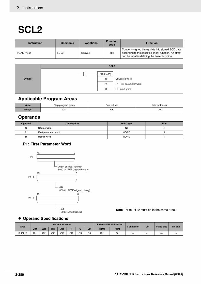
2 Instructions
SCL2
Applicable Program Areas
Operands
P1: First Parameter Word
Operand Specifications
Instruction Mnemonic VariationsFunction
codeFunction
SCALING 2 SCL2 @SCL2 486Converts signed binary data into signed BCD data according to the specified linear function. An offset can be input in defining the linear function.
Symbol
SCL2
Area Step program areas Subroutines Interrupt tasks
Usage OK OK OK
Operand Description Data type Size
S Source word INT 1
P1 First parameter word WORD 3
R Result word WORD 1
Note P1 to P1+2 must be in the same area.
Area Word addresses Indirect DM addresses
Constants CF Pulse bits TR bitsCIO WR HR AR T C DM @DM *DM
S, P1, R OK OK OK OK OK OK OK OK OK --- --- --- ---
S: Source word
P1: First parameter word
R: Result word
SCL2(486)
S
P1
R
P1
P1+1
P1+2
15 0
15 0
15 0
Offset of linear function8000 to 7FFF (signed binary)
8000 to 7FFF (signed binary)
0000 to 9999 (BCD)
2-280 CP1E CPU Unit Instructions Reference Manual(W483)

2 Instructions D
ata Co
ntro
l Instru
ction
s
2
SC
L2
Flags
FunctionSCL2(486) is used to convert the signed binary data contained in the source word S into signed BCDdata (the BCD data contains the absolute value and the Carry Flag shows the sign) and place the resultin the result word R according to the linear function defined by the slope (∆X, ∆Y) and an offset. Theaddress of the first word containing ∆X, ∆Y, and the offset is specified for the first parameter word P1.The sign of the result is indicated by the status of the Carry Flag (ON: negative, OFF: positive).
The following equations are used for the conversion.
The offset and slope can be a positive value, 0, or a negative value. Using a negative slope enablesreverse scaling.
• The result will be rounded to the nearest integer.
• The result in R will be the absolute BCD conversion value and the sign will be indicated by the CarryFlag. The result can thus be between –9999 and 9999.
• If the result is less than –9999, –9999 will be output as the result. If the result is greater than 9999,9999 will be output.
Name Label Operation
Error Flag P_ER • ON if the contents of C+1 (∆X) is 0000.
• ON if the contents of C+2 (∆Y) is not BCD.
• OFF in all other cases.
Equals Flag P_EQ • ON if the result is 0.
• OFF in all other cases.
Carry Flag P_CY • ON if the result is negative.
• OFF if the result is zero or positive.
R =∆Y
× [(BCD conversion of S) – (BCD conversion of offset)]BCD conversion of ∆X
Note The slope of the line is ∆Y/∆X.
P1
P1+1
P1+2
R (signed BCD)
S (signed binary)
Offset
R (signed BCD)
S (signed binary)
Offset
R (signed BCD)
S (signed binary)
Offset of 0000
Offset = 0000 hex
Offset
∆Y
∆X
(Signed binary)
(Signed binary)
(Signed BCD)
Positive Offset Negative Offset
∆Y
∆X
∆Y
∆X
∆Y
∆X
2-281CP1E CPU Unit Instructions Reference Manual(W483)

2 Instructions
Hint• SCL2(486) can be used to scale the results of analog signal conversion values from Analog Input
Units according to user-defined scale parameters. For example, if a 1 to 5-V input to an Analog InputUnit is input to memory as 0000 to 0FA0 hexadecimal, the value in memory can be scaled to –100 to200°C using SCL2(486).
• SCL2(486) converts signed binary to signed BCD. Negative values can thus be handled directly for S.The result of scaling in R and the Carry Flag can also be used to output negative values for the scal-ing result.
Sample program Scaling 1 to 5-V Analog Input to 0 to 300
In the following example, it is assumed that an analog signal from 1 to 5 V is converted and input to CIO3 as 0000 to 1770 hexadecimal. SCL2(486) is used to convert (scale) the value in CIO 3 to a valuebetween 0000 and 0300 BCD.
When CIO 0.00 is ON, the contents of CIO 3 is scaled using the linear function defined by ∆X (1770),∆Y (0300), and the offset (0). These values are contained in D100 to D102, and the result is output toD200.
SCL2
3
D100
D200
0.00
S
P1
R
P1: D100
P1+1:D101
P1+2:D102
Offset
∆X
∆Y
FED4
0.8V
0300
0000-0015
0315
1770
5V
0000
1V
189C
5.2V
Contents of R (D200)
Contents of S (CIO 3)
∆Y
1770Hex(∆X)
0 0 0 0
1 7 7 0
0 3 0 0
2-282 CP1E CPU Unit Instructions Reference Manual(W483)

2 Instructions D
ata Co
ntro
l Instru
ction
s
2
SC
L2
Scaling 1 to 5-V Analog Input to –200 to 200In the following example, it is assume that an analog signal from 1 to 5 V is converted and input to CIO3 as 0000 to 1770 hexadecimal. SCL2(486) is used to convert (scale) the value in CIO 3 to a valuebetween –0200 and 0200 BCD.
When CIO 0.00 is ON, the contents of CIO 3 is scaled using the linear function defined by ∆X (1770),∆Y (0400), and the offset (07D0). These values are contained in D100 to D102, and the result is outputto D200.
SCL2
3
D100
D200
0.00
S
P1
R
FED4
0.8V
0200
0000
0220
1770
5V
0000
1V
189C
5.2V
1770 Hex (∆X)
-0200
-0220
0400(∆Y)Contents of S (CIO 200)
P1: D100
P1+1:D101
P1+2:D102
Contents of R(D200)
Offset
∆X
∆Y
0 7 D 0
1 7 7 0
0 4 0 0
Offset07D0 Hex
2-283CP1E CPU Unit Instructions Reference Manual(W483)

2 Instructions
SCL3
Applicable Program Areas
Operands
P1: First Parameter Word
Instruction Mnemonic VariationsFunction
codeFunction
SCALING 3 SCL3 @SCL3 487Converts signed BCD data into signed binary data according to the specified linear function. An offset can be input in defining the linear function.
Symbol
SCL3
Area Step program areas Subroutines Interrupt tasks
Usage OK OK OK
Operand Description Data type Size
S Source word WORD 1
P1 First parameter word WORD 5
R Result word INT 1
Note P1 to P1+4 must be in the same area.
S: Source word
P1: First parameter word
R: Result word
SCL3(487)
S
P1
R
P1
P1+1
P1+2
P1+3
P1+4
15 0
15 0
15 0
15 0
15 0
∆X
∆Y
Offset of linear function 8000 to 7FFF (signed binary)
0001 to 9999 (BCD)
8000 to 7FFF (signed binary)
Maximum conversion8000 to 7FFF (signed binary)
Minimum conversion 8000 to 7FFF (signed binary)
2-284 CP1E CPU Unit Instructions Reference Manual(W483)
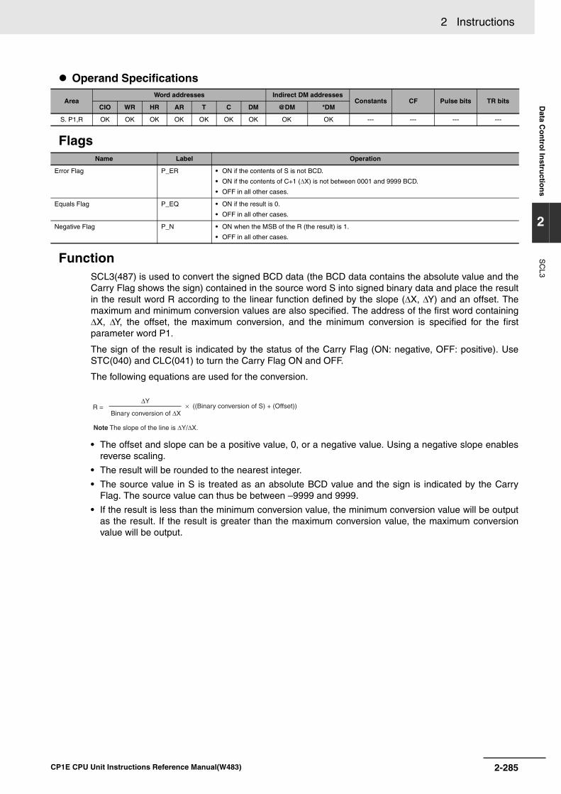
2 Instructions D
ata Co
ntro
l Instru
ction
s
2
SC
L3
Operand Specifications
Flags
FunctionSCL3(487) is used to convert the signed BCD data (the BCD data contains the absolute value and theCarry Flag shows the sign) contained in the source word S into signed binary data and place the resultin the result word R according to the linear function defined by the slope (∆X, ∆Y) and an offset. Themaximum and minimum conversion values are also specified. The address of the first word containing∆X, ∆Y, the offset, the maximum conversion, and the minimum conversion is specified for the firstparameter word P1.
The sign of the result is indicated by the status of the Carry Flag (ON: negative, OFF: positive). UseSTC(040) and CLC(041) to turn the Carry Flag ON and OFF.
The following equations are used for the conversion.
• The offset and slope can be a positive value, 0, or a negative value. Using a negative slope enablesreverse scaling.
• The result will be rounded to the nearest integer.
• The source value in S is treated as an absolute BCD value and the sign is indicated by the CarryFlag. The source value can thus be between –9999 and 9999.
• If the result is less than the minimum conversion value, the minimum conversion value will be outputas the result. If the result is greater than the maximum conversion value, the maximum conversionvalue will be output.
Area Word addresses Indirect DM addresses
Constants CF Pulse bits TR bitsCIO WR HR AR T C DM @DM *DM
S. P1,R OK OK OK OK OK OK OK OK OK --- --- --- ---
Name Label Operation
Error Flag P_ER • ON if the contents of S is not BCD.
• ON if the contents of C+1 (∆X) is not between 0001 and 9999 BCD.
• OFF in all other cases.
Equals Flag P_EQ • ON if the result is 0.
• OFF in all other cases.
Negative Flag P_N • ON when the MSB of the R (the result) is 1.
• OFF in all other cases.
R =∆Y
× ((Binary conversion of S) + (Offset))Binary conversion of ∆X
Note The slope of the line is ∆Y/∆X.
2-285CP1E CPU Unit Instructions Reference Manual(W483)

2 Instructions
HintSCL3(487) is used to convert data using a user-defined scale to signed binary for Analog Output Units.For example, SCL3(487) can convert 0 to 200 °C to 0000 to 1770 (hex) and output an analog outputsignal 1 to 5 V from the Analog Output Unit.
Sample programWhen a value from 0 to 200 is scaled to an analog signal (1 to 5 V, for example), a signed BCD value of0000 to 0200 is converted (scaled) to signed binary value of 0000 to 1770 for an Analog Output Unit.When CIO 0.00 turns ON in the following example, the contents of D0 is scaled using the linear functiondefined by ∆X (0200), ∆Y (1770), and the offset (0). These values are contained in D100 to D102. Thesign of the BCD value in D0 is indicated by the Carry Flag. The result is output to CIO 103.
S (signed BCD)
Offset Offset
S (signed BCD)
Offset of 0000
Positive Offset
R (signed binary)
R (signed binary)
R (signed binary)
Negative Offset
Max conversion
Min. conversion
Max conversion
Min. conversion
Max conversion
Min. conversion
S (signed BCD)
∆X
∆Y
∆X
∆Y
∆X
∆Y
SCL3
D0
D100
103
0.00
S
P1
R
P1 :D100
P1+1:D101
P1+2:D102
P1+3:D103
P1+4:D104
Offset
∆X
∆Y
Max. conversion
Min. conversion
0000
-010
1770189C
0200 2010∆X(0200)
∆Y(1770 Hex)
FED4
Contents of R (2011, signed binary)
Contents of S (D0, signed BCD)
0 0 0 0
0 2 0 0
1 7 7 0
1 8 9 C
F E D 4
2-286 CP1E CPU Unit Instructions Reference Manual(W483)

2 Instructions D
ata Co
ntro
l Instru
ction
s
2
AV
G
AVG
Applicable Program Areas
Operands
N: Number of CyclesThe number of cycles must be between 0001 and 0040 hexadecimal (0 to 64 cycles).
R: Result First Word and R+1: First Work Area Word
Note R to R+N+1 must be in the same area.
Operand Specifications
Flags
Instruction Mnemonic VariationsFunction
codeFunction
AVERAGE AVG --- 195Calculates the average value of an input word for the specified number of cycles.
Symbol
AVG
Area Step program areas Subroutines Interrupt tasks
Usage OK OK OK
Operand Description Data type Size
S Source word UINT 1
N Number of cycles UINT 1
R Result first word UINT Variable
Area Word addresses Indirect DM addresses
Constants CF Pulse bits TR bitsCIO WR HR AR T C DM @DM *DM
S, NOK OK OK OK OK OK OK OK OK
OK--- --- ---
R ---
Name Label Operation
Error Flag P_ER • ON if the contents of N is 0.
• OFF in all other cases.
S: Source word
N: Number of cycles
R: Result first word
AVG(195)
S
N
R
R+1
R+2:
15 014
R+N+1:
Used by system.
Previous value #1
Previous value #N
R: AverageR+1: Processing information
Average Valid FlagOFF: Not valid (AVG(195) has not yet been executed the specified number of cycles.)ON: Valid.
2-287CP1E CPU Unit Instructions Reference Manual(W483)
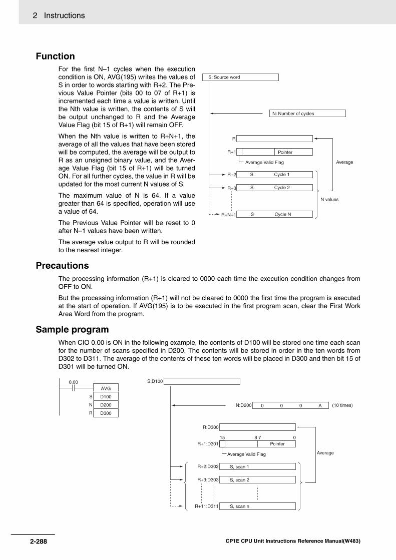
2 Instructions
Function
PrecautionsThe processing information (R+1) is cleared to 0000 each time the execution condition changes fromOFF to ON.
But the processing information (R+1) will not be cleared to 0000 the first time the program is executedat the start of operation. If AVG(195) is to be executed in the first program scan, clear the First WorkArea Word from the program.
Sample programWhen CIO 0.00 is ON in the following example, the contents of D100 will be stored one time each scanfor the number of scans specified in D200. The contents will be stored in order in the ten words fromD302 to D311. The average of the contents of these ten words will be placed in D300 and then bit 15 ofD301 will be turned ON.
For the first N–1 cycles when the executioncondition is ON, AVG(195) writes the values ofS in order to words starting with R+2. The Pre-vious Value Pointer (bits 00 to 07 of R+1) isincremented each time a value is written. Untilthe Nth value is written, the contents of S willbe output unchanged to R and the AverageValue Flag (bit 15 of R+1) will remain OFF.
When the Nth value is written to R+N+1, theaverage of all the values that have been storedwill be computed, the average will be output toR as an unsigned binary value, and the Aver-age Value Flag (bit 15 of R+1) will be turnedON. For all further cycles, the value in R will beupdated for the most current N values of S.
The maximum value of N is 64. If a valuegreater than 64 is specified, operation will usea value of 64.
The Previous Value Pointer will be reset to 0after N–1 values have been written.
The average value output to R will be roundedto the nearest integer.
R+N+1
R
R+1
R+2
R+3
S Cycle 1
S Cycle 2
S Cycle N
Average
N values
Average Valid Flag
S: Source word
N: Number of cycles
Pointer
AVG
D100
D200
D300
0.00
S
N
R
N:D200 (10 times)
S:D100
R:D300
R+1:D301
R+2:D302
R+3:D303
R+11:D311
AverageAverage Valid Flag
15 78 0Pointer
0 0 0 A
S, scan 1
S, scan 2
S, scan n
2-288 CP1E CPU Unit Instructions Reference Manual(W483)
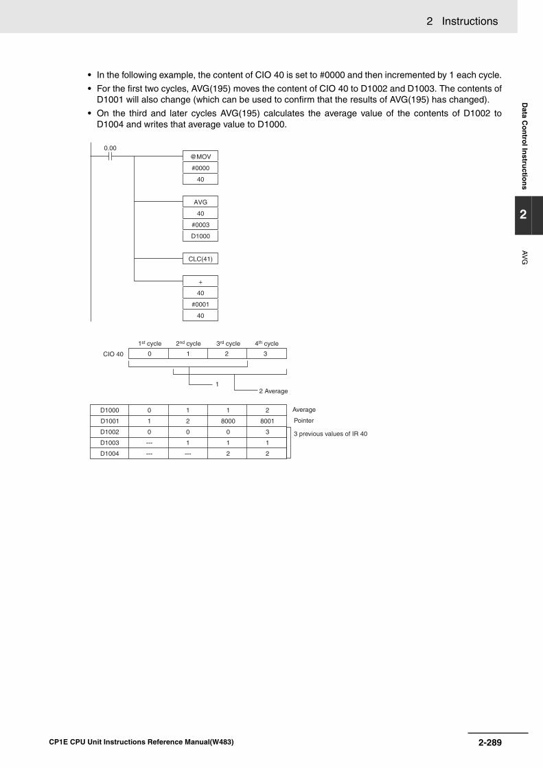
2 Instructions D
ata Co
ntro
l Instru
ction
s
2
AV
G
• In the following example, the content of CIO 40 is set to #0000 and then incremented by 1 each cycle.
• For the first two cycles, AVG(195) moves the content of CIO 40 to D1002 and D1003. The contents ofD1001 will also change (which can be used to confirm that the results of AVG(195) has changed).
• On the third and later cycles AVG(195) calculates the average value of the contents of D1002 toD1004 and writes that average value to D1000.
D1000 0 1 1 2
D1001 1 2 8000 8001
D1002 0 0 0 3
D1003 --- 1 1 1
D1004 --- --- 2 2
CIO 40 0 1 2 3
1st cycle 2nd cycle 3rd cycle 4th cycle
Average
Pointer
3 previous values of IR 40
2 Average1
@MOV
#0000
40
+
40
#0001
40
AVG
40
#0003
D1000
CLC(41)
0.00
2-289CP1E CPU Unit Instructions Reference Manual(W483)

2 Instructions
Subroutines Instructions
SBS
Applicable Program Areas
Operands
N: Subroutine numberSpecifies the subroutine number between 0 and 127 decimal.
Operand Specifications
Combined-use instructionsSBN (subroutine entry) instructions and RET (subroutine return) instructions
Flags
Instruction Mnemonic VariationsFunction
codeFunction
SUBROUTINE CALL SBS @SBS 091Calls the subroutine with the specified subroutine number and executes that program.
Symbol
SBS
Area Step program areas Subroutines Interrupt tasks
Usage OK OK OK
Operand Description Data type Size
N Subroutine number --- 1
Area Word addresses Indirect DM addresses
Constants CF Pulse bits TR bitsCIO WR HR AR T C DM @DM *DM
N --- --- --- --- --- --- --- --- --- OK --- --- ---
Name Label Operation
Error Flag P_ER • ON if nesting exceeds 16 levels.
• ON if the specified subroutine number does not exist.
• ON if a subroutine calls itself.
• ON if a subroutine being executed is called.
• ON if the specified subroutine is not defined in the current task.
• OFF in all other cases.
N: Subroutine number
SBS(091)
N
2-290 CP1E CPU Unit Instructions Reference Manual(W483)

2 Instructions S
ub
rou
tines In
structio
ns
2
SB
S
FunctionSBS(091) calls the subroutine with thespecified subroutine number. The subrou-tine is the program section betweenSBN(092) and RET(093). When the sub-routine is completed, program executioncontinues with the next instruction afterSBS(091).A subroutine can be called more thanonce in a program.
Subroutines can be nested up to 16 lev-els. Nesting is when another subroutine iscalled from within a subroutine program,such as shown in the following example,which is nested to 3 levels.
B
SBS
n
A
B
A
SBN
n
RET
END
Main program
Subroutine program (SBN(092) to RET(093))
Program end
Execution condition ON
SBN 10
to to
to
toto
SBS 11
RET
SBN 11
SBS 12
RET RET
SBN 12D
SBS
n
C
D
A
SBN
n
RET
A
SBS
m
B
SBN
m
RET
END
Main program
Subroutine program n
Execution condition ON
Execution condition ON
C
BSubroutine program m
Program end
Two-levelnesting
2-291CP1E CPU Unit Instructions Reference Manual(W483)
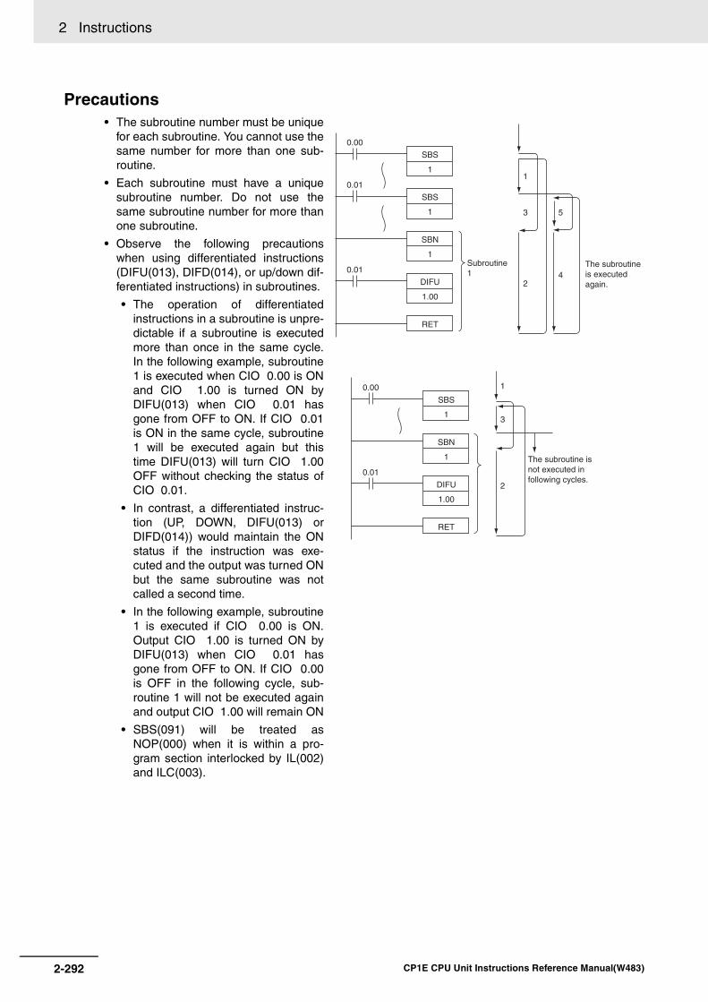
2 Instructions
Precautions• The subroutine number must be unique
for each subroutine. You cannot use thesame number for more than one sub-routine.
• Each subroutine must have a uniquesubroutine number. Do not use thesame subroutine number for more thanone subroutine.
• Observe the following precautionswhen using differentiated instructions(DIFU(013), DIFD(014), or up/down dif-ferentiated instructions) in subroutines.
• The operation of differentiatedinstructions in a subroutine is unpre-dictable if a subroutine is executedmore than once in the same cycle.In the following example, subroutine1 is executed when CIO 0.00 is ONand CIO 1.00 is turned ON byDIFU(013) when CIO 0.01 hasgone from OFF to ON. If CIO 0.01is ON in the same cycle, subroutine1 will be executed again but thistime DIFU(013) will turn CIO 1.00OFF without checking the status ofCIO 0.01.
• In contrast, a differentiated instruc-tion (UP, DOWN, DIFU(013) orDIFD(014)) would maintain the ONstatus if the instruction was exe-cuted and the output was turned ONbut the same subroutine was notcalled a second time.
• In the following example, subroutine1 is executed if CIO 0.00 is ON.Output CIO 1.00 is turned ON byDIFU(013) when CIO 0.01 hasgone from OFF to ON. If CIO 0.00is OFF in the following cycle, sub-routine 1 will not be executed againand output CIO 1.00 will remain ON
• SBS(091) will be treated asNOP(000) when it is within a pro-gram section interlocked by IL(002)and ILC(003).
SBS
1
Subroutine 1
0.00
SBS
1
0.01
SBN
1
DIFU
1.00
0.01
RET
1
3 5
42
The subroutine is executed again.
SBS
1
0.00
SBN
1
DIFU
1.00
0.01
RET
1
3
The subroutine is not executed in following cycles.
2
2-292 CP1E CPU Unit Instructions Reference Manual(W483)
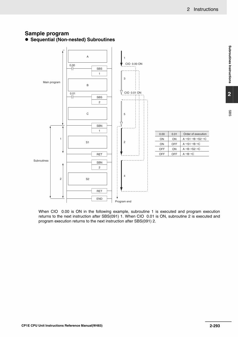
2 Instructions S
ub
rou
tines In
structio
ns
2
SB
S
Sample program Sequential (Non-nested) Subroutines
When CIO 0.00 is ON in the following example, subroutine 1 is executed and program executionreturns to the next instruction after SBS(091) 1. When CIO 0.01 is ON, subroutine 2 is executed andprogram execution returns to the next instruction after SBS(091) 2.
B
SBS
1
S1
A
SBS
2
RET
C
SBN
1
S2
SBN
2
RET
END
1
3
5
2
4
CIO 0.00 ON
1
2
0.00
0.01
0.00
ON
ON
OFF
OFF
Order of execution
A→S1→B→S2→C
A→S1→B→C
A→B→S2→C
A→B→C
0.01
ON
OFF
ON
OFF
CIO 0.01 ON
Program end
Main program
Subroutines
2-293CP1E CPU Unit Instructions Reference Manual(W483)

2 Instructions
Nested Subroutines
When CIO 0.00 is ON in the following example, subroutine 1 is executed. If CIO 0.01 is ON, subroutine2 is executed from within subroutine 1 and program execution returns to the next instruction afterSBS(091) 2 when subroutine 2 is completed. Execution of subroutine 1 continues and program execu-tion returns to the next instruction after SBS(091) 1 when subroutine 1 is completed.
B
SBS
1
S1-2
A
SBN
1
RET
S1-1
SBS
2
S2
SBN
2
RET
END
1
5
2
4
3
CIO 0.00 ON
CIO 0.00 ON
0.00
0.01Subroutine 1
Subroutine 2
0.00
ON
ON
OFF
OFF
Order of execution
A→S1-1→S2→S1-2→B
A→S1-1→S1-2→B
A→B
A→B
0.01
ON
OFF
ON
OFF
2-294 CP1E CPU Unit Instructions Reference Manual(W483)
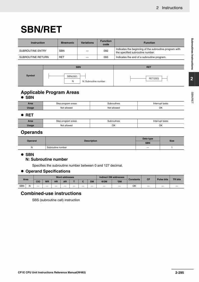
2 Instructions S
ub
rou
tines In
structio
ns
2
SB
N/R
ET
SBN/RET
Applicable Program Areas SBN
RET
Operands
SBNN: Subroutine number
Specifies the subroutine number between 0 and 127 decimal.
Operand Specifications
Combined-use instructionsSBS (subroutine call) instruction
Instruction Mnemonic VariationsFunction
codeFunction
SUBROUTINE ENTRY SBN --- 092Indicates the beginning of the subroutine program with the specified subroutine number.
SUBROUTINE RETURN RET --- 093 Indicates the end of a subroutine program.
Symbol
SBN RET
Area Step program areas Subroutines Interrupt tasks
Usage Not allowed Not allowed OK
Area Step program areas Subroutines Interrupt tasks
Usage Not allowed OK OK
Operand Description Data type
SizeSBN
N Subroutine number --- 1
Area Word addresses Indirect DM addresses
Constants CF Pulse bits TR bitsCIO WR HR AR T C DM @DM *DM
SBN N --- --- --- --- --- --- --- --- --- OK --- --- ---
N: Subroutine number
SBN(092)
NRET(093)
2-295CP1E CPU Unit Instructions Reference Manual(W483)

2 Instructions
Flags SBN/RET
There are no flags affected by this instruction.
Function SBN
RETWhen program execution reaches RET(093), it is automatically returned to the next instruction after theSBS(091) instruction that called the subroutine.
Precautions• Place the subroutine program area (SBN(092) to RET(093)) in the same task as the SBS(091)
instruction of the same number. Subroutines in other tasks cannot be called.
SBN(092) indicates the beginning of the sub-routine with the specified subroutine number.The end of the subroutine is indicated byRET(093).The region of the program beginning at thefirst SBN(092) instruction is the subroutineregion. A subroutine is executed only when ithas been called by SBS(091) .
SBS
n
SBN
n
RET
Subroutineregion
SBS
n
SBN
n
RET
END
Task
OK
SBS
n
END
SBN
n
RET
END
Task 1
Not allowed
Task 2
2-296 CP1E CPU Unit Instructions Reference Manual(W483)
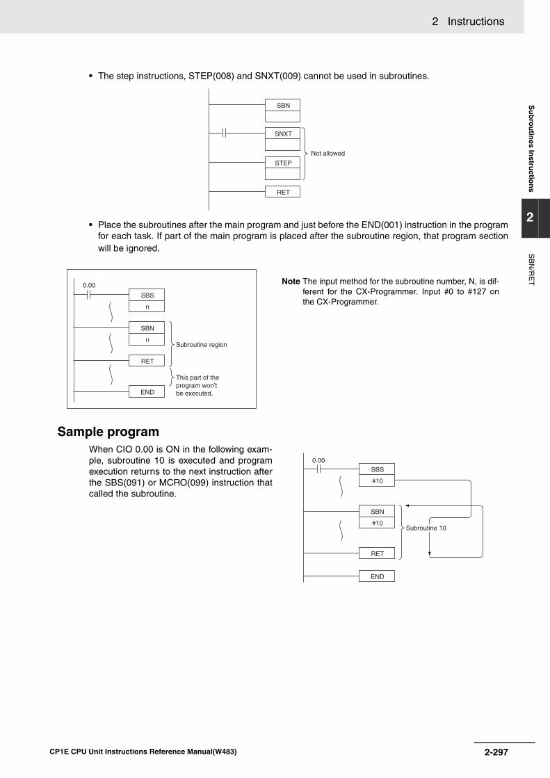
2 Instructions S
ub
rou
tines In
structio
ns
2
SB
N/R
ET
• The step instructions, STEP(008) and SNXT(009) cannot be used in subroutines.
• Place the subroutines after the main program and just before the END(001) instruction in the programfor each task. If part of the main program is placed after the subroutine region, that program sectionwill be ignored.
Sample program
Note The input method for the subroutine number, N, is dif-ferent for the CX-Programmer. Input #0 to #127 onthe CX-Programmer.
When CIO 0.00 is ON in the following exam-ple, subroutine 10 is executed and programexecution returns to the next instruction afterthe SBS(091) or MCRO(099) instruction thatcalled the subroutine.
SBN
SNXT
STEP
RET
Not allowed
END
Subroutine region
This part of the program won’t be executed.
SBS
n
0.00
SBN
n
RET
SBS
#10
0.00
SBN
#10
RET
END
Subroutine 10
2-297CP1E CPU Unit Instructions Reference Manual(W483)

2 Instructions
Interrupt Control Instructions
CP1E CPU Units support the following interrupts.
Outline of Interrupt Control Instructions SET INTERRUPT MASK: MSKS(690)
Both I/O interrupt tasks and scheduled interrupt tasks are masked (disabled) when the PLC enters RUNmode. MSKS(690) can be used to unmask or mask I/O interrupts and set the time intervals for sched-uled interrupts.
CLEAR INTERRUPT: CLI(691)CLI(691) clears or retains recorded interrupt inputs for I/O interrupts or sets the time to the first sched-uled interrupt for scheduled interrupts. It also clears or retains recorded high-speed counter interrupts.
DISABLE INTERRUPTS: DI(693)DI(693) disables execution of all interrupt tasks.
ENABLE INTERRUPTS: EI(694)EI(694) enables execution of all interrupt tasks.
Precautions in Using Interrupt Tasks Precautions for All Interrupts
• When multiple interrupts occur at once, the order of execution of the interrupts is as follows:I/O interrupt > scheduled interrupt
Note “A > B” indicates that A is given priority over B. On the same interrupt level, lower numbered tasks are givenpriority over higher numbered tasks.
Precautions for I/O Interrupts• Only built-in inputs from CP1E CPU Units are supported for interrupt tasks.
• Use interrupt inputs on the CPU Rack from 0ch02 bit to 0ch07 bit. I/O interrupt tasks will not be exe-cuted if using any other input.
• All interrupt inputs that have been detected will be cleared when the interrupt mask is cleared.
• There is no limit on the number of I/O interrupt inputs that can be recorded, but only one interrupt isrecorded for each I/O interrupt number. Furthermore, the recorded interrupt is not cleared until itsinterrupt task has been completed, so a new interrupt input will be ignored if it is received while itsinterrupt task is being executed.
Precautions for Scheduled Interrupts• Be sure that the time interval is longer than the time required to execute the scheduled interrupt task.
• To accurately control the time to the first interrupt and the interrupt interval, program CLI(691) to setthe time to the first schedule interrupt just before programming MSKS(690). If MSKS(690) is used torestart a schedule interrupt, the time to the first scheduled interrupt will be accurate even if CLI(691)is not used.
• The time unit for the scheduled interrupt is always 0.1ms.
Type Execution condition Setting procedure
I/O Interrupts Interrupt input from the built-in Input on the CPU Rack turns ON/OFF.
Use the MSKS instruction to assign inputs from Interrupt Input on the CPU Rack.
Scheduled Interrupts Scheduled (fixed intervals) Use the MSKS instruction to set the interrupt interval.
2-298 CP1E CPU Unit Instructions Reference Manual(W483)

2 Instructions In
terrup
t Co
ntro
l Instru
ction
s
2
Related Memory Area WordsName Address Operation
Maximum Interrupt Task Processing Time
A440 The maximum processing time for an interrupt task is stored in binary data in 0.1-ms units and is cleared at the start of operation.
Interrupt Task with Maximum Processing Time
A441 The interrupt task number with maximum processing time is stored in binary data. Here, 8000 to 800F Hex correspond to task numbers 00 to 0F Hex.
A441.15 will turn ON when the first interrupt occurs after the start of operation. The maximum process-ing time for subsequent interrupt tasks will be stored in the rightmost two digits in hexadecimal and will be cleared at the start of operation.
2-299CP1E CPU Unit Instructions Reference Manual(W483)

2 Instructions
MSKS
Applicable Program Areas
Operands
(1) I/O Interrupt Task
Note When the up/down differentiation setting is changed, all detected interrupt inputs will be cleared.
(2) Resetting and Starting Scheduled Interrupts
Instruction Mnemonic VariationsFunction
codeFunction
SET INTERRUPT MASK MSKS @MSKS 690Controls whether I/O interrupt tasks and sched-uled interrupt tasks are executed.
Symbol
MSKS
Area Step program areas Subroutines Interrupt tasks
Usage OK OK OK
Operand Description Data type Size
N Interrupt identifier --- 1
C Control data UINT 1
OperandContents
Disabling/Enabling Interrupt Input Setting Specifying Up/Down Differentiation of an Interrupt Input
N
I/O Interrupt No. I/O Interrupt No.
102: Interrupt input 2 (interrupt task 2)
103: Interrupt input 3 (interrupt task 3)
104: Interrupt input 4 (interrupt task 4)
105: Interrupt input 5 (interrupt task 5)
106: Interrupt input 6 (interrupt task 6)
(Cannot be used in CP1E-E10D-)
107: Interrupt input 7 (interrupt task 7)
(Cannot be used in CP1E-E10D-)
112: Interrupt input 2 (interrupt task 2)
113: Interrupt input 3 (interrupt task 3)
114: Interrupt input 4 (interrupt task 4)
115: Interrupt input 5 (interrupt task 5)
116: Interrupt input 6 (interrupt task 6)
(Cannot be used in CP1E-E10D-)
117: Interrupt input 7 (interrupt task 7)
(Cannot be used in CP1E-E10D-)
C
Interrupt Mask Interrupt Mask
0000 hex: Enable (unmask) the interrupt (direct mode).
0001 hex: Disable (mask) the interrupt (direct mode).
0000 hex: Up-differentiation (Detect rising edge.)
0001 hex: Down-differentiation (Detect falling edge.)
Operand Contents
NScheduled Interrupt No.
4 or 14: Scheduled interrupt 0 (interrupt task 1)
C
Scheduled interrupt time units Scheduled interrupt set time
Any time unit setting 0 decimal (0000 hex):
Disable interrupt. (Stop internal timer.)
0.1 ms 10 to 9,999 decimal (000A to 270F hex):Enable interrupt. (Reset internal timer value, and then start timer with interrupt interval between 1.0 and 999.9 ms.)
Note Settings 0001 to 000A cannot be used. An error will occur if one of these settings is used.
N: Interrupt identifier
C: Control data
MSKS(690)
N
C
2-300 CP1E CPU Unit Instructions Reference Manual(W483)

2 Instructions In
terrup
t Co
ntro
l Instru
ction
s
2
MS
KS
Operand Specifications
Flags
FunctionWhen the program execution starts, the interrupt inputs that generate I/O interrupt tasks are masked(disabled), and the internal timers creating the timer interrupts that generate scheduled interrupt tasksare stopped.
Use MSKS(690) to enable the I/O interrupts and timer interrupts, so that the corresponding interrupttasks can be executed.
The value of N specifies the interrupt task and the kind of processing that will be performed.
(1) N = 102 to 107: Enabling/Disabling the Interrupt Inputs of I/O Interrupt Tasks
• Enables or disables the interrupt inputs specified by N, based on the status of the bits in C. Withthis function, MSKS(690) can control whether or not each task is executed.
• When an interrupt input is enabled, any interrupts detected up to that point will be cleared.
(2) N = 112 to 117: Specifying the Differentiation of Interrupt Inputs
• Specifies whether the interrupt inputs specified by N are up-differentiated or down-differentiated,based on the status of the bits in C.
• Use the differentiation specification together with the enabling/disabling function. If MSKS(690) isnot executed to specify up or down differentiation, the interrupt inputs are up-differentiated (thedefault setting).
• When MSKS(690) is executed to specify an interrupt input’s up or down differentiation, any inter-rupts detected up to that point will be cleared.
(3) N = 4 or 14: Resetting and Restarting Scheduled Interrupt Tasks
• Sets the time interval (specified by C) for the specified scheduled interrupt task (specified by N),resets the internal timer’s PV, and starts the internal timer. Since the internal timer’s PV is reset,this function maintains the proper interval from the execution of MSKS(690) until the start of thefirst interrupt .
HintThe longest interrupt task processing time is stored in A440 (Maximum Interrupt Task ProcessingTime). At the same time, the task number of the interrupt task with the longest interrupt task processingtime is stored in A441 (Interrupt Task with Maximum Processing Time).
Area Word addresses Indirect DM addresses
Constants CF Pulse bits TR bitsCIO WR HR AR T C DM @DM *DM
N --- --- --- --- --- --- --- --- ---OK --- --- ---
C OK OK OK OK OK OK OK OK OK
Name Label Operation
Error Flag P_ER ON if N is not within the specified range.
Errors when specifying I/O Interrupts:
• The Error Flag will go ON if C is not within the specified range.Errors when specifying Scheduled Interrupts:
• The Error Flag will go ON if C is not between 10 and 9,999 decimal (000A to 270F hex).
OFF in all other cases.
2-301CP1E CPU Unit Instructions Reference Manual(W483)

2 Instructions
Precaution• Be sure that the time interval is longer than the time required to execute the scheduled interrupt task.
• To accurately control the time to the first interrupt and the interrupt interval, program CLI(691) to setthe time to the first schedule interrupt just before programming MSKS(690). If MSKS(690) is used torestart a schedule interrupt, however, the time to the first scheduled interrupt will be accurate even ifCLI(691) is not used.
• During the execution of a scheduled interrput, the scheduled interrupt set time cannot be changed.Please change the scheduled interrupt set time after disable interrupt (stop internal timer) is set withMSKS instruction.
Sample program Examples for Input Interrupts
When W0.00 turns ON in the following example, the first MSKS(690) (1) specifies generating inputinterrupts for input interrupt 3 when the interrupt input turns ON and the second MSKS(690) (2)unmasks the interrupt.
Example for Scheduled InterruptsWhen W0.01 turns ON in the following example, MSKS(690) sets the schedule interrupt interval forschedule interrupt 0 to 10.5 ms (assuming the unit is set to 0.1 ms in the PLC Setup), resets the internaltimer, and starts the internal timer.
W0.00
N
S
MSKS
113
#0000
MSKS
103
#0000
N
S
(1)
(2)
MSKS
14
&105
W0.01
N
S
2-302 CP1E CPU Unit Instructions Reference Manual(W483)

2 Instructions In
terrup
t Co
ntro
l Instru
ction
s
2
CLI
CLI
Applicable Program Areas
Operands
(1) Clearing/Retaining an I/O Interrupt Task’s Recorded Interrupt Inputs
(2) Setting the Time to the First Scheduled Interrupts
Instruction Mnemonic VariationsFunction
codeFunction
CLEAR INTERRUPT CLI @CLI 691Clears/retains recorded interrupt inputs, sets the time to the first scheduled interrupt for scheduled interrupt tasks.
Symbol
CLI
Area Step program areas Subroutines Interrupt tasks
Usage OK OK OK
Operand Description Data type Size
N Interrupt number --- 1
C Control data UINT 1
Operand Contents
N
Interrupt Input No.
102: Interrupt input 2 (interrupt task 2)
103: Interrupt input 3 (interrupt task 3)
104: Interrupt input 4 (interrupt task 4)
105: Interrupt input 5 (interrupt task 5)
106: Interrupt input 6 (interrupt task 6) (Cannot be used in CP1E-E10D-)
107: Interrupt input 7 (interrupt task 7) (Cannot be used in CP1E-E10D-)
C
Recorded Interrupt
0000 hex: Retain the recorded interrupt.
0001 hex: Clear the recorded interrupt.
Operand Contents
NScheduled Interrupt No.
4: Interrupt task 0 (interrupt task 1)
C
Scheduled interrupt time units (Set in the PLC Setup.)
Scheduled interrupt set time
0.1 ms 10 to 9,999 decimal (000A to 270F hex):Sets time to first interrupt between 1.0 and 999.9 ms.
N: Interrupt number
C: Control data
CLI(691)
N
C
2-303CP1E CPU Unit Instructions Reference Manual(W483)

2 Instructions
(3) Clearing/Retaining High-speed Counter Interrupts
Operand Specifications
Flags
FunctionDepending on the value of N, CLI(691) clears the specified recorded I/O interrupts, sets the time beforeexecution of the first scheduled interrupt, or clears the specified recorded high-speed counter inter-rupts.
(1) N = 102 to 107: Clearing Interrupt Inputs
CLI(691) clears a recorded interrupt input specified by N, when the corresponding bit of C is ONand retains the recorded interrupt input when the corresponding bit is OFF.
If an I/O interrupt task is being executed and an interrupt input with a different interrupt number isreceived, that interrupt number is recorded internally. The recorded I/O interrupts are executedlater in order of their priority (from the lowest number to the highest).
If you want to ignore interrupt inputs that are received while an interrupt task is being executed, useCLI(691) to clear the recorded interrupts before they are executed.
Operand Contents
N
High-speed Counter Input
10: High-speed counter input 0
11: High-speed counter input 1
12: High-speed counter input 2
13: High-speed counter input 3
14: High-speed counter input 4
15: High-speed counter input 5 (Cannot be used in CP1E-E10D-)
C
Recorded Interrupt
0000 hex: Retain the recorded interrupt.
0001 hex: Clear the recorded interrupt.
Area Word addresses Indirect DM addresses
Constants CF Pulse bits TR bitsCIO WR HR AR T C DM @DM *DM
N --- --- --- --- --- --- --- --- ---OK --- --- ---
C OK OK OK OK OK OK OK OK OK
Name Label Operation
Error Flag P_ER • ON if N is not within the specified range.
• ON if C is not 0000 or 0001 hex (for I/O interrupts or high-speed counter interrupts).
• ON if C is not within the specified range of 10 to 9,999 decimal (000A to 270F hex) for scheduled interrupts.
• OFF in all other cases.
Interrupt input n
Internal status
Recorded interrupt retainedRecorded interrupt cleared
Internal status
Interrupt input n
2-304 CP1E CPU Unit Instructions Reference Manual(W483)

2 Instructions In
terrup
t Co
ntro
l Instru
ction
s
2
CLI
(2) N = 4: Setting the Time to the First Scheduled Interrupt Task
When N is 4, the content of C specifies the time interval to the first scheduled interrupt task.
(3) N = 10 or 15: Clearing High-speed Counter Interrupts
When N is 10 or 15, CLI(691) clears or retains the recorded high-speed counter interrupt (targetcomparison) specified by N.
Sample program Example for Input Interrupts
When W0.00 turns ON in the following example, CLI(691) clears all interrupts stored for input interrupt 2.
Example for First Scheduled InterruptsWhen W0.01 turns ON in the following example, CLI(691) sets the time to the first schedule interrupt10.5 ms (0069 hex = 105 decimal).
Example for High-speed Counter InterruptsWhen W0.02 turns ON in the following example, CLI(691) clears all interrupts stored for high-speedcounter interrupt 0.
Execution of scheduled interrupt task.
Time to first scheduled interrupt
MSKS(690)
CLI
102
#0001
W0.00
N
S
CLI
4
D1100
W0.01
N
S D1100
015
90 60
CLI
10
#0001
W0.02
N
S
2-305CP1E CPU Unit Instructions Reference Manual(W483)

2 Instructions
DI
Applicable Program Areas
Flags
FunctionDI(693) is executed from the main program to temporarily disable all interrupt tasks (I/O interrupts,scheduled interrupts).
PrecautionsAll interrupt tasks will remain disabled until EI(694) is executed.
DI(693) cannot be executed from an interrupt task.
Sample program
Instruction Mnemonic VariationsFunction
codeFunction
DISABLE INTERRUPTS DI @DI 693Disables execution of all interrupt tasks except the power OFF interrupt.
Symbol
DI
Area Step program areas Subroutines Interrupt tasks
Usage OK OK Not allowed
Name Label Operation
Error Flag P_ER • ON if DI(693) is executed from an interrupt task.
• OFF in all other cases.
When CIO 0.00 is ON in the following example,DI(693) disables all interrupt tasks.
DI(693)
Disables execution of all interrupt tasks
0.00
DI
2-306 CP1E CPU Unit Instructions Reference Manual(W483)

2 Instructions In
terrup
t Co
ntro
l Instru
ction
s
2
EI
EI
Applicable Program Areas
Flags
Function• EI(694) is executed from the main program to temporarily enable all interrupt tasks that were disabled
by DI(693). DI(693) disables all interrupts (I/O interrupts, scheduled interrupts).
Precautions• EI(694) does not require an execution condition. It is always executed with an ON execution condi-
tion.
• EI(694) enables the interrupt tasks that were disabled by DI(693). It cannot unmask I/O interrupts thathave not been unmasked by MSKS(690) or set scheduled interrupts that have not been set byMSKS(690).
• EI(694) cannot be executed in an interrupt task.
Sample program
Instruction Mnemonic VariationsFunction
codeFunction
ENABLE INTERRUPTS EI --- 694Enables execution of all interrupt tasks that were disabled with DI(693).
Symbol
EI
Area Step program areas Subroutines Interrupt tasks
Usage OK OK Not allowed
Name Label Operation
Error Flag P_ER • ON if EI(694) is executed from an interrupt task.
• OFF in all other cases.
EI(694)
Disables execution of all interrupt tasks.
Enables execution of all disabled interrupt tasks.
0.00
EI
DI
2-307CP1E CPU Unit Instructions Reference Manual(W483)
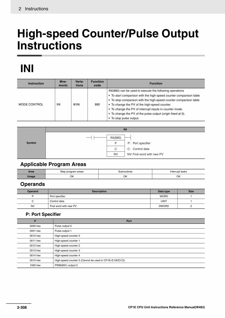
2 Instructions
High-speed Counter/Pulse Output Instructions
INI
Applicable Program Areas
Operands
P: Port Specifier
InstructionMne-
monicVaria-tions
Function code
Function
MODE CONTROL INI @INI 880
INI(880) can be used to execute the following operations
• To start comparison with the high-speed counter comparison table
• To stop comparison with the high-speed counter comparison table
• To change the PV of the high-speed counter.
• To change the PV of interrupt inputs in counter mode.
• To change the PV of the pulse output (origin fixed at 0).
• To stop pulse output.
Symbol
INI
Area Step program areas Subroutines Interrupt tasks
Usage OK OK OK
Operand Description Data type Size
P Port specifier WORD 1
C Control data UINT 1
NV First word with new PV DWORD 2
P Port
0000 hex Pulse output 0
0001 hex Pulse output 1
0010 hex High-speed counter 0
0011 hex High-speed counter 1
0012 hex High-speed counter 2
0013 hex High-speed counter 3
0014 hex High-speed counter 4
0015 hex High-speed counter 5 (Cannot be used in CP1E-E10D-)
1000 hex PWM(891) output 0
NV: First word with new PV
INI(880)
P
C
NV
P: Port specifier
C: Control data
2-308 CP1E CPU Unit Instructions Reference Manual(W483)

2 Instructions H
igh
-speed
Co
un
ter/Pu
lseO
utp
ut In
structio
ns
2
INI
C: Control Data
NV: First Word with New PV
Operand Specifications
Flags
FunctionINI(880) performs the operation specified in C for the port specified in P. The possible combinations ofoperations and ports are shown in the following table.
Starting Comparison (C = 0000 hex)If C is 0000 hex, INI(880) starts comparison of a high-speed counter’s PV to the comparison table reg-istered with CTBL(882).
Note A target value comparison table must be registered in advance with CTBL(882). If INI(880) is executed with-out registering a table, the Error Flag will turn ON.
Stopping Comparison (C = 0001 hex)If C is 0001 hex, INI(880) stops comparison of a high-speed counter’s PV to the comparison table regis-tered with CTBL(882).
C INI(880) function
0000 hex Starts comparison.
0001 hex Stops comparison.
0002 hex Changes the PV.
0003 hex Stops pulse output.
If C is 0002 hex (i.e., when changing a PV),NV and NV+1 contain the new PV. Any val-ues in NV and NV+1 are ignored when C isnot 0002 hex.
Area Word addresses Indirect DM addresses
Constants CF Pulse bits TR bitsCIO WR HR AR T C DM @DM *DM
P, C --- --- --- --- --- --- --- --- --- OK--- --- ---
NV OK OK OK OK OK OK OK OK OK ---
Name Label Operation
Error Flag P_ER • ON if the specified range for P, C, or NV is exceeded.
• ON if the combination of P and C is not allowed.
• ON if a comparison table has not been registered but starting comparison is specified.
• ON if a new PV is specified for a port that is currently outputting pulses.
• ON if changing the PV of a high-speed counter is specified for a port that is not specified for a high-speed counter.
• ON if INI(880) is executed in an interrupt task for a high-speed counter and an interrupt occurs when CTBL(882) is executed.
• OFF in all other cases.
P: Port specifier
C: Control data
0000 hex: Start comparison
0001 hex: Stop comparison
0002 hex: Change PV
0003 hex: Stop pulse output
0000 or 0001 hex: Pulse output Not allowed. Not allowed. OK OK
0010 to 0015 hex: High-speed counter input OK OK OK Not allowed.
1000 hex: PWM (891) output Not allowed. Not allowed. Not allowed. OK
NV
NV+1
015
For Pulse Output or High-speed Counter Input: 0000 0000 to FFFF FFFF hex
Lower word of new PV
Upper word of new PV
2-309CP1E CPU Unit Instructions Reference Manual(W483)

2 Instructions
Changing a PV (C = 0002 hex)
Stopping Pulse Output (P = 0000, 0001 or 1000 hex and C = 0003 hex)If C is 0003 hex, INI(880) immediately stops pulse output for the specified port. If this instruction is exe-cuted when pulse output is already stopped, then the pulse amount setting will be cleared.
Sample programWhen CIO 0.00 turns ON in the following example, SPED(885) starts outputting pulses from pulse out-put 0 in Continuous Mode at 500 Hz. When CIO 0.01 turns ON, pulse output is stopped by INI(880).
i
Port and mode Operation Setting range
Pulse output (P = 0000 or 0001 hex)
The present value of the pulse output is changed. The new value is specified in NV and NV+1.
Note This instruction can be executed only when pulse output is stopped. An error will occur if it is executed during pulse output.
8000 0000 to 7FFF FFFF hex (-2,147,483,648 to 2,147,483,647)
High-speed counter input (P = 0010 to 0015 hex)
Linear Mode
Differential inputs, increment/decre-ment pulses, or pulse + direction inputs
The present value of the high-speed counter is changed. The new value is specified in NV and NV+1.
Note An error will occur for the instruction if the specified port is not set for a high-speed counter.
8000 0000 to 7FFF FFFF hex (-2,147,483,648 to 2,147,483,647)
Increment pulse input0000 0000 to FFFF FFFF hex (0 to 4,294,967,295)
Ring Mode0000 0000 to FFFF FFFF hex (0 to 4,294,967,295)
@SPED
#0000
#0100
D100
01F4
0
0.00
@INI
#0000
#0003
0
0.01
D100
D101Pulse output 0Target frequency: 500 Hz
Pulse output 0
Stop pulse output
(Not used.)
Pulse + Direction output, CW, Continuous Mode
2-310 CP1E CPU Unit Instructions Reference Manual(W483)
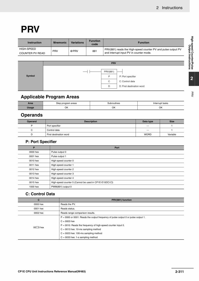
2 Instructions H
igh
-speed
Co
un
ter/Pu
lseO
utp
ut In
structio
ns
2
PR
V
PRV
Applicable Program Areas
Operands
P: Port Specifier
C: Control Data
Instruction Mnemonic VariationsFunction
codeFunction
HIGH-SPEED
COUNTER PV READPRV @PRV 881
PRV(881) reads the High-speed counter PV and pulse output PV and interrupt input PV in counter mode.
Symbol
PRV
Area Step program areas Subroutines Interrupt tasks
Usage OK OK OK
Operand Description Data type Size
P Port specifier --- 1
C Control data --- 1
D First destination word WORD Variable
P Port
0000 hex Pulse output 0
0001 hex Pulse output 1
0010 hex High-speed counter 0
0011 hex High-speed counter 1
0012 hex High-speed counter 2
0013 hex High-speed counter 3
0014 hex High-speed counter 4
0015 hex High-speed counter 5 (Cannot be used in CP1E-E10D-)
1000 hex PWM(891) output 0
C PRV(881) function
0000 hex Reads the PV.
0001 hex Reads status.
0002 hex Reads range comparison results.
00 3 hex
P = 0000 or 0001: Reads the output frequency of pulse output 0 or pulse output 1.
C = 0003 hex
P = 0010: Reads the frequency of high-speed counter input 0.
C = 0013 hex: 10-ms sampling method
C = 0023 hex: 100-ms sampling method
C = 0033 hex: 1-s sampling method
D: First destination word
PRV(881)
P
C
D
P: Port specifier
C: Control data
2-311CP1E CPU Unit Instructions Reference Manual(W483)
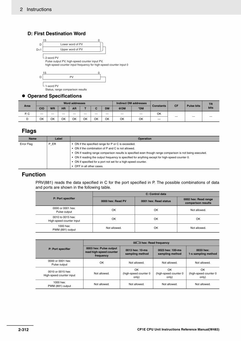
2 Instructions
D: First Destination Word
Operand Specifications
Flags
FunctionPRV(881) reads the data specified in C for the port specified in P. The possible combinations of dataand ports are shown in the following table.
Area Word addresses Indirect DM addresses
Constants CF Pulse bitsTR bitsCIO WR HR AR T C DM @DM *DM
P, C --- --- --- --- --- --- --- --- --- OK--- --- ---
D OK OK OK OK OK OK OK OK OK ---
Name Label Operation
Error Flag P_ER • ON if the specified range for P or C is exceeded.
• ON if the combination of P and C is not allowed.
• ON if reading range comparison results is specified even though range comparison is not being executed.
• ON if reading the output frequency is specified for anything except for high-speed counter 0.
• ON if specified for a port not set for a high-speed counter.
• OFF in all other cases.
P: Port specifier
C: Control data
0000 hex: Read PV 0001 hex: Read status0002 hex: Read range comparison results
0000 or 0001 hex: Pulse output
OK OK Not allowed.
0010 to 0015 hex: High-speed counter input
OK OK OK
1000 hex: PWM (891) output
Not allowed. OK Not allowed.
P: Port specifier
00 3 hex: Read frequency
0003 hex: Pulse output read high-speed counter
frequency
0013 hex: 10-ms sampling method
0023 hex: 100-ms sampling method
0033 hex: 1-s sampling method
0000 or 0001 hex: Pulse output
OK Not allowed. Not allowed. Not allowed.
0010 or 0015 hex: High-speed counter input
Not allowed.OK
(high-speed counter 0 only)
OK(high-speed counter 0
only)
OK(high-speed counter 0
only)
1000 hex: PWM (891) output
Not allowed. Not allowed. Not allowed. Not allowed.
D
D+1
015
D PV
015
Lower word of PV
Upper word of PV
2-word PVPulse output PV, high-speed counter input PV, high-speed counter input frequency for high-speed counter input 0
1-word PVStatus, range comparison results
2-312 CP1E CPU Unit Instructions Reference Manual(W483)

2 Instructions H
igh
-speed
Co
un
ter/Pu
lseO
utp
ut In
structio
ns
2
PR
V
Reading a PV (C = 0000 hex)
Reading Status (C = 0001 hex)
Port and mode Operation Setting range
Pulse output (P = 0000 or 0001 hex) The present value of the pulse output is stored in D and D+1.
8000 0000 to 7FFF FFFF hex (−2,147,483,648 to 2,147,483,647)
High-speed counter input (P = 0010 to 0015 hex)
Linear Mode The present value of the high-speed counter is stored in D and D+1.
8000 0000 to 7FFF FFFF hex (−2,147,483,648 to 2,147,483,647)
Ring Mode 0000 0000 to FFFF FFFF hex (0 to 4,294,967,295)
Port and mode Operation Results of reading
Pulse output The pulse output status is stored in D.
High-speed counter input The high-speed counter status is stored in D.
PWM(891) output The PWM(891) output is stored in D.
Reading the Results of Range Comparison (C = 0002 hex)
If C is 0002 hex, PRV(881) reads the results ofrange comparison and stores it in D as shown inthe following diagram.
015
D 0 0 0 0 0 0 0 0
Pulse Output Stopped Error Flag OFF: No error ON: Pulse output stopped due to error
Pulse Output Status Flag OFF: Constant speed ON: Accelerating/deceleratingPV Overflow/Underflow Flag OFF: Normal ON: Error
Pulse Output Amount Set Flag OFF: Not set ON: SetPulse Output Completed Flag OFF: Output not completed ON: Output completed
Pulse Output In-progress Flag OFF: Stopped ON: OutputtingNo-origin Flag OFF: Origin established ON: Origin not established
At-origin Flag OFF: Not stopped at origin ON: Stopped at origin
015D 0 0 0 0 0 0 0 0 0 0 0 0 0
Comparison In-progress Flag OFF: Stopped ON: Comparing
PV Overflow/Underflow Flag OFF: Normal ON: Error
Count Direction OFF: Decrementing ON: Incrementing
015
D 0 0 0 0 0 0 0 0 0 0 0 0 0 0 0
Pulse Output In-progress Flag OFF: Stopped ON: Outputting
015
D 0 0 0 0 0 0 0 0 0 0
Comparison Result 1 OFF: Not in range ON: In range
Comparison Result 2 OFF: Not in range ON: In range
Comparison Result 3 OFF: Not in range ON: In range
Comparison Result 4 OFF: Not in range ON: In range
Comparison Result 5 OFF: Not in range ON: In range
Comparison Result 6 OFF: Not in range ON: In range
2-313CP1E CPU Unit Instructions Reference Manual(W483)

2 Instructions
Reading Pulse Output or High-speed Counter Frequency (C = 00@3 hex)If C is 00@3 hex, PRV(881) reads the frequency being output from pulse output 0 or 1 or the frequencybeing input to high-speed counter 0 and stores it in D and D+1.
0000 or 0001 hex (Reading the frequency of pulse output 0 or 1)
0000 0000 to 0001 86A0 hex (0 to 100,000)
0010 hex (Reading the frequency of high-speed counter 0)
Counter input method: Any input method other than 4× differential phase mode:
Result = 00000000 to 000186A0 hex (0 to 100,000)
Note If a frequency higher than 100 kHz has been input, the output will remain at the maximum value of 000186A0hex.
Counter input method: 4× differential phase mode:
Result = 00000000 to 00030D40 hex (0 to 200,000)
Note If a frequency higher than 200 kHz has been input, the output will remain at the maximum value of00030D40 hex.
Pulse Frequency Calculation MethodsThe function counts the number of pulses within a fixed interval (the sampling time) and calculates thefrequency from that count. One of the following three sampling times can be selected by setting therightmost two digits of C.
PrecautionsIf the counter is reset when P is 0010 hex (high-speed counter 0) and C is 0013, 0023, or 0033 hex(sampling method), the data read during the sampling time when the counter was reset will not bedependable.
Sample program
Sampling time Value of C Description
10 ms 0013 hex Counts the number of pulses every 10 ms. The error is 10% max. at 1 kHz.
100 ms 0023 hex Counts the number of pulses every 100 ms. The error is 1% max. at 1 kHz.
1 s 0033 hex Counts the number of pulses every 1 s. The error is 0.1% max. at 1 kHz.
When CIO 0.00 turns ON in the followingprogramming example, CTBL(882) registersa range comparison table for high-speedcounter 0 and starts comparison. When CIO0.01 turns ON, PRV(881) reads the rangecomparison results at that time and storesthem in CIO 0100.
When CIO 1.00 turns ON in the followingprogramming example, PRV(881) reads thefrequency of the pulse being input to high-speed counter 0 at that time and stores it asa hexadecimal value in D200 and D201.
@CTBL
#0000
#0001
D100
0.00
@PRV
#0010
#0002
100
0.01
Range comparison table registration and comparison start
High-speed counter input 0
High-speed counter input 0
Read range comparison results
PRV
#0010
#0013
D200
1.00
Read input frequency
High-speed counter input 0
2-314 CP1E CPU Unit Instructions Reference Manual(W483)

2 Instructions H
igh
-speed
Co
un
ter/Pu
lseO
utp
ut In
structio
ns
2
CT
BL
CTBL
Applicable Program Areas
Operands
P: Port specifier
C: Control data
Instruction Mnemonic VariationsFunction
codeFunction
REGISTER COMPARISON TABLE
CTBL @CTBL 882CTBL(882) is used to register a comparison table and perform comparisons for a high-speed counter PV.
Symbol
CTBL
Area Step program areas Subroutines Interrupt tasks
Usage OK OK OK
Operand Description Data type Size
P Port specifier --- 1
C Control data --- 1
TB First comparison table word LWORD Variable
P Port
0000 hex High-speed counter 0
0001 hex High-speed counter 1
0002 hex High-speed counter 2
0003 hex High-speed counter 3
0004 hex High-speed counter 4
0005 hex High-speed counter 5 (Cannot be used in CP1E-E10D-)
C CTBL(882) function
0000 hex Registers a target value comparison table and starts comparison.
0001 hex Registers a range comparison table and performs one comparison.
0002 hex Registers a target value comparison table. Comparison is started with INI(880).
0003 hex Registers a range comparison table. Comparison is started with INI(880).
P: Port specifier
CTBL(882)
P
C
TB TB: First comparison table word
C: Control data
2-315CP1E CPU Unit Instructions Reference Manual(W483)

2 Instructions
TB: First comparison table word• TB is the first word of the comparison table. The structure of the comparison table depends on the
type of comparison being performed. For target value comparison, the length of the comparison table is determined by the number of tar-get values specified in TB. The table can be between 4 and 19 words long, as shown below.
• For range comparison, the comparison table always contains six ranges. The table is 30 words long,as shown below. If it is not necessary to set six ranges, set the interrupt task number to FFFF hex forall unused ranges.
Note Always set the upper limit greater than or equal to the lower limit for any one range.
Operand Specifications
Area Word addresses Indirect DM addresses
Constants CF Pulse bits TR bitsCIO WR HR AR T C DM @DM *DM
P, C --- --- --- --- --- --- --- --- --- OK--- --- ---
TB OK OK OK OK OK OK OK OK OK ---
TB+1
TB+2
TB+3
TB
015
03478
0 0 0 0
11121415
TB+16
TB+17
TB+18
Upper word of target value 1
Interrupt task number for target value 1
00000000 to FFFFFFFF hex
00000000 to FFFFFFFF hex
Number of target values 0001 to 6 hex (1 to 6 target values)
Interrupt Task Number
Interrupt task number 00 to 0F hex (0 to 15)Direction
OFF: Incrementing, ON: Decrementing
Upper word of target value 6
Interrupt task number for target value 6
Lower word of target value 1
Lower word of target value 6
TB
TB+1
TB+2
TB+3
015
TB+25
TB+26
TB+27
TB+28
TB+29
Range 1 interrupt task number
0000 0000 to FFFF FFFF hex (See note.)
0000 0000 to FFFF FFFF hex (See note.)
0000 0000 to FFFF FFFF hex (See note.)
0000 0000 to FFFF FFFF hex (See note.)
Interrupt task number 0000 to 000F hex: Interrupt task number 0 to 15AAAA hex: Do not execute interrupt task. FFFF hex: Ignore the settings for this range.
Lower word of range 1 lower limit
Upper word of range 1 lower limit
Lower word of range 1 upper limit
Upper word of range 1 upper limit
Range 6 interrupt task number
Lower word of range 6 lower limit
Upper word of range 6 lower limit
Lower word of range 6 upper limit
Upper word of range 6 upper limit
2-316 CP1E CPU Unit Instructions Reference Manual(W483)
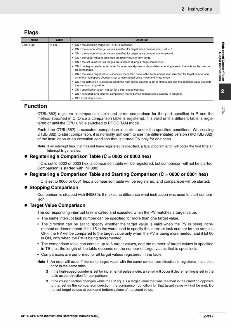
2 Instructions H
igh
-speed
Co
un
ter/Pu
lseO
utp
ut In
structio
ns
2
CT
BL
Flags
FunctionCTBL(882) registers a comparison table and starts comparison for the port specified in P and themethod specified in C. Once a comparison table is registered, it is valid until a different table is regis-tered or until the CPU Unit is switched to PROGRAM mode.
Each time CTBL(882) is executed, comparison is started under the specified conditions. When usingCTBL(882) to start comparison, it is normally sufficient to use the differentiated version (@CTBL(882))of the instruction or an execution condition that is turned ON only for one scan.
Note If an interrupt task that has not been registered is specified, a fatal program error will occur the first time aninterrupt is generated.
Registering a Comparison Table (C = 0002 or 0003 hex)If C is set to 0002 or 0003 hex, a comparison table will be registered, but comparison will not be started.Comparison is started with INI(880).
Registering a Comparison Table and Starting Comparison (C = 0000 or 0001 hex)If C is set to 0000 or 0001 hex, a comparison table will be registered, and comparison will be started.
Stopping ComparisonComparison is stopped with INI(880). It makes no difference what instruction was used to start compar-ison.
Target Value ComparisonThe corresponding interrupt task is called and executed when the PV matches a target value.
• The same interrupt task number can be specified for more than one target value.
• The direction can be set to specify whether the target value is valid when the PV is being incre-mented or decremented. If bit 15 in the word used to specify the interrupt task number for the range isOFF, the PV will be compared to the target value only when the PV is being incremented, and if bit 00is ON, only when the PV is being decremented.
• The comparison table can contain up to 6 target values, and the number of target values is specifiedin TB (i.e., the length of the table depends on the number of target values that is specified).
• Comparisons are performed for all target values registered in the table.
Note 1 An error will occur if the same target value with the same comparison direction is registered more thanonce in the same table.
2 If the high-speed counter is set for incremental pulse mode, an error will occur if decrementing is set in thetable as the direction for comparison.
3 If the count direction changes while the PV equals a target value that was reached in the direction oppositeto that set as the comparison direction, the comparison condition for that target value will not be met. Donot set target values at peak and bottom values of the count value.
Name Label Operation
Error Flag P_ER • ON if the specified range for P or C is exceeded.
• ON if the number of target values specified for target value comparison is set to 0.
• ON if the number of target values specified for target value comparison exceeds 6.
• ON if the upper value is less than the lower value for any range.
• ON if the set values for all ranges are disabled during a range comparison.
• ON if the high-speed counter is set for incremental pulse mode and decrementing is set in the table as the direction for comparison.
• ON if the same target value is specified more than once in the same comparison direction for target comparison when the high-speed counter is set to incremental pulse mode and linear mode.
• ON if an instruction is executed when the high-speed counter is set to Ring Mode and the specified value exceeds the maximum ring value.
• ON if specified for a port not set for a high-speed counter.
• ON if executed for a different comparison method while comparison is already in progress.
• OFF in all other cases.
2-317CP1E CPU Unit Instructions Reference Manual(W483)
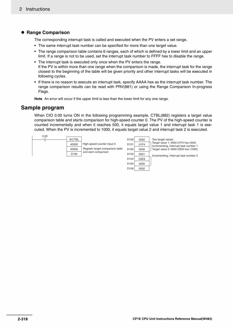
2 Instructions
Range ComparisonThe corresponding interrupt task is called and executed when the PV enters a set range.
• The same interrupt task number can be specified for more than one target value.
• The range comparison table contains 6 ranges, each of which is defined by a lower limit and an upperlimit. If a range is not to be used, set the interrupt task number to FFFF hex to disable the range.
• The interrupt task is executed only once when the PV enters the range.If the PV is within more than one range when the comparison is made, the interrupt task for the rangeclosest to the beginning of the table will be given priority and other interrupt tasks will be executed infollowing cycles.
• If there is no reason to execute an interrupt task, specify AAAA hex as the interrupt task number. Therange comparison results can be read with PRV(881) or using the Range Comparison In-progressFlags.
Note An error will occur if the upper limit is less than the lower limit for any one range.
Sample programWhen CIO 0.00 turns ON in the following programming example, CTBL(882) registers a target valuecomparison table and starts comparison for high-speed counter 0. The PV of the high-speed counter iscounted incrementally and when it reaches 500, it equals target value 1 and interrupt task 1 is exe-cuted. When the PV is incremented to 1000, it equals target value 2 and interrupt task 2 is executed.
@CTBL
#0000
#0000
D100
0002
01F4
0000
0001
03E8
0000
0002
0.00D100
D101
D102
D103
D104
D105
D106
Two target valuesTarget value 1: 0000 01F4 hex (500)Incrementing, Interrupt task number 1Target value 2: 0000 03E8 hex (1000)
Incrementing, Interrupt task number 2
Register target comparison table and start comparison
High-speed counter input 0
2-318 CP1E CPU Unit Instructions Reference Manual(W483)
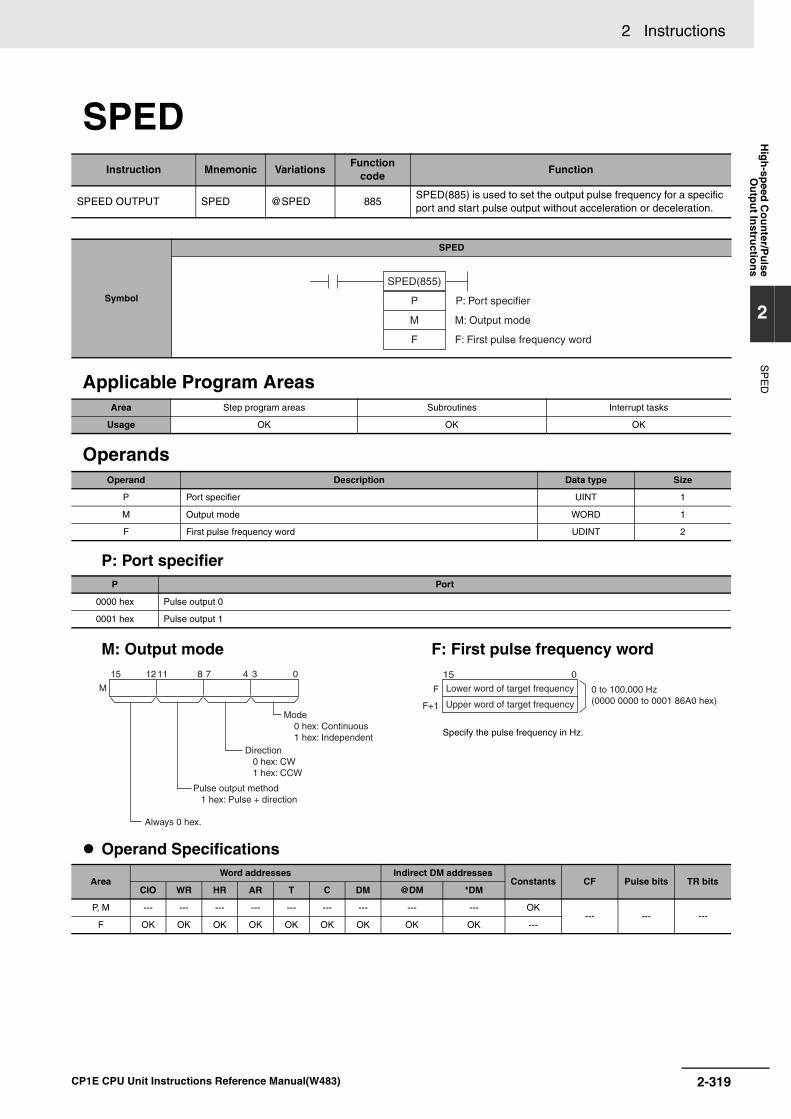
2 Instructions H
igh
-speed
Co
un
ter/Pu
lseO
utp
ut In
structio
ns
2
SP
ED
SPED
Applicable Program Areas
Operands
P: Port specifier
Operand Specifications
Instruction Mnemonic VariationsFunction
codeFunction
SPEED OUTPUT SPED @SPED 885SPED(885) is used to set the output pulse frequency for a specific port and start pulse output without acceleration or deceleration.
Symbol
SPED
Area Step program areas Subroutines Interrupt tasks
Usage OK OK OK
Operand Description Data type Size
P Port specifier UINT 1
M Output mode WORD 1
F First pulse frequency word UDINT 2
P Port
0000 hex Pulse output 0
0001 hex Pulse output 1
M: Output mode F: First pulse frequency word
Specify the pulse frequency in Hz.
Area Word addresses Indirect DM addresses
Constants CF Pulse bits TR bitsCIO WR HR AR T C DM @DM *DM
P, M --- --- --- --- --- --- --- --- --- OK--- --- ---
F OK OK OK OK OK OK OK OK OK ---
F: First pulse frequency word
SPED(855)
P
M
F
P: Port specifier
M: Output mode
03478111215
M
Mode 0 hex: Continuous 1 hex: Independent
Direction 0 hex: CW 1 hex: CCW
Pulse output method 1 hex: Pulse + direction
Always 0 hex.
F
F+1
015
Lower word of target frequency
Upper word of target frequency
0 to 100,000 Hz (0000 0000 to 0001 86A0 hex)
2-319CP1E CPU Unit Instructions Reference Manual(W483)

2 Instructions
Flags
Function
In independent mode, pulse output will stop automatically when the number of pulses set withPULS(886) in advance have been output. In continuous mode, pulse output will continue until stoppedfrom the program.An error will occur if the mode is changed between independent and continuous mode while pulses arebeing output.
Note SPED instruction can be used only with transistor output type of CP1E N/NA-type CPU Unit.In case of transistor output type of CP1E E-type CPU Unit or relay output type, NOP processing is applied.
Continuous Mode Speed ControlWhen continuous mode operation is started, pulse output will be continued until it is stopped from theprogram.
Note Pulse output will stop immediately if the CPU Unit is changed to PROGRAM mode.
Name Label Operation
Error Flag P_ER • ON if the specified range for P, M, or F is exceeded.
• ON if PLS2(887) or ORG(889) is already being executed to control pulse output for the specified port.
• ON if SPED(885) or INI(880) is used to change the mode between continuous and independent output during pulse output.
• ON if SPED(885) is executed in an interrupt task when an instruction controlling pulse output is being executed in a cyclic task.
• ON if SPEC(885) is executed in independent mode with an absolute number of pulses and the origin has not been established.
• OFF in all other cases.
SPED(885) starts pulse output on the portspecified in P using the method specified inM at the frequency specified in F. Pulse out-put will be started each time SPED(885) isexecuted. It is thus normally sufficient to usethe differentiated version (@SPED(885)) ofthe instruction or an execution conditionthat is turned ON only for one scan.
Operation Purpose Application Frequency changes DescriptionProcedure/instruction
Starting pulse output
To output with speci-fied speed
Changing the speed (fre-quency) in one step
Outputs pulses at a specified frequency.
SPED(885) (Continu-ous)
Changing settings
To change speed in one step
Changing the speed during operation
Changes the fre-quency (higher or lower) of the pulse out-put in one step.
SPED(885) (Continu-ous)
↓
SPED(885) (Continu-ous)
Target frequency
Time
SPED(885) executed.
Pulse frequency
Pulse frequency
Target frequency
Execution of SPED(885)
Time
Pulse frequency
Target frequency
Present frequency
Execution of SPED(885)
Time
2-320 CP1E CPU Unit Instructions Reference Manual(W483)

2 Instructions H
igh
-speed
Co
un
ter/Pu
lseO
utp
ut In
structio
ns
2
SP
ED
Independent Mode PositioningWhen independent mode operation is started, pulse output will be continued until the specified numberof pulses has been output.Note • Pulse output will stop immediately if the CPU Unit is changed to PROGRAM mode.
• The number of output pulses must be set each time output is restarted.
• The number of output pulses must be set in advance with PULS(881). Pulses will not be output forSPED(885) if PULS(881) is not executed first.
• The direction set in the SPED(885) operand will be ignored if the number of pulses is set with PULS(881)as an absolute value.
Stopping pulse output
Stop pulse output
Immediate stop Stops the pulse output immediately.
SPED(885) (Continu-ous)
↓
INI(880)
Stop pulse output
Immediate stop Stops the pulse output immediately.
SPED(885) (Continu-ous)
↓
SPED(885) (Continu-ous, Target frequency of 0 Hz)
Operation Purpose Application Frequency changes DescriptionProcedure/instruction
Starting pulse output
To output with specified speed
Positioning without accel-eration or deceleration
Starts outputting pulses at the specified fre-quency and stops immediately when the specified number of pulses has been out-put.
Note The target posi-tion (number of pulses) cannot be changed during positioning (pulse output).
PULS(886)
↓
SPED(885) (Independent)
Changing settings
To change speed in one step
Changing the speed in one step during operation
SPED(885) can be exe-cuted during position-ing to change (raise or lower) the pulse output frequency in one step.
The target position (specified number of pulses) is not changed.
PULS(886)
↓
SPED(885) (Independent)
↓
SPED(885) (Independent)
Operation Purpose Application Frequency changes DescriptionProcedure/instruction
Pulse frequency
Present frequency
Execution of INI(880)
Time
Pulse frequency
Present frequency
Execution of SPED(885)
Time
Pulse frequency
Target frequency
Specified number of pulses (Specified with PULS(886).)
Execution of SPED(885)
Outputs the specified number of pulses and then stops.
Time
Pulse frequency
New target frequency
Original target frequency
Specified number of pulses (Specified with PULS(886).) Number of pulses
specified with PULS(886) does not change.
Execution of SPED(885) (independent mode)
SPED(885) (independent mode) executed again to change the target frequency. (The target position is not changed.)
Time
2-321CP1E CPU Unit Instructions Reference Manual(W483)
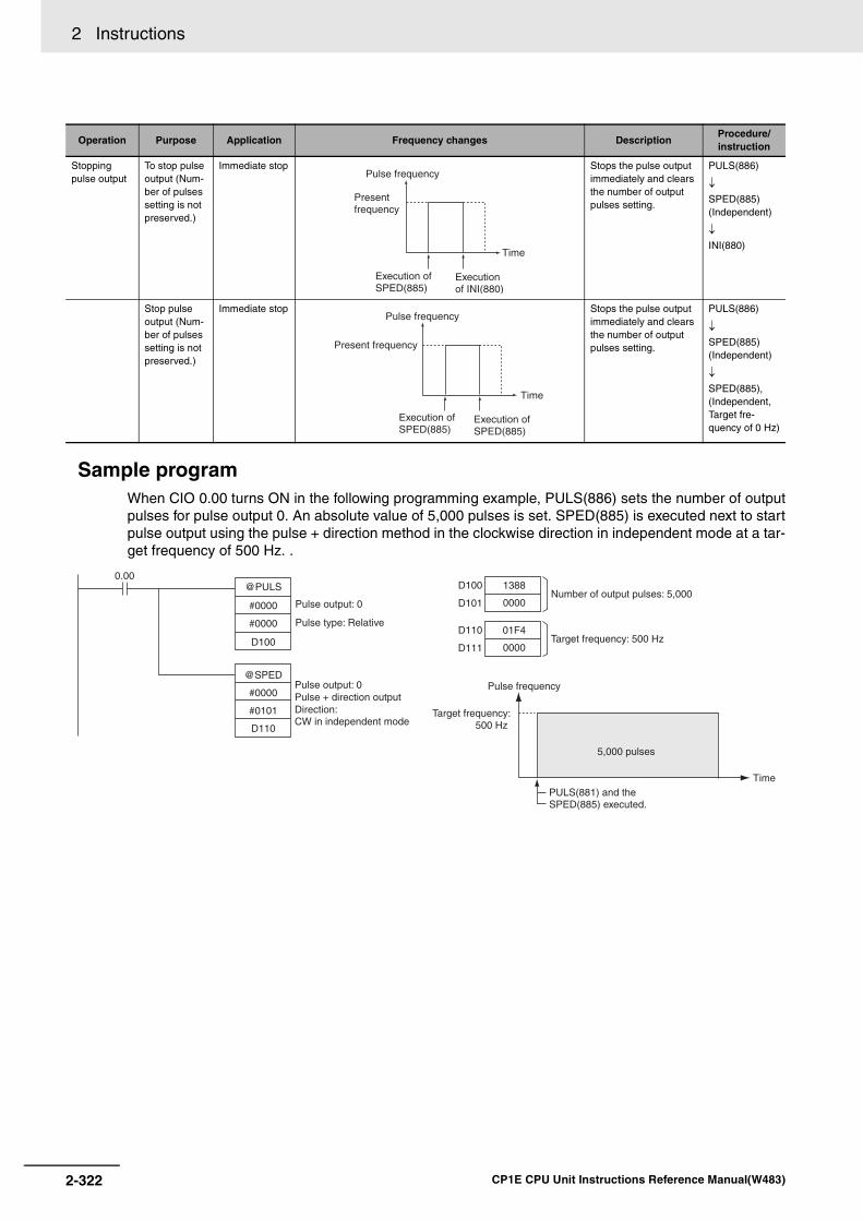
2 Instructions
Sample programWhen CIO 0.00 turns ON in the following programming example, PULS(886) sets the number of outputpulses for pulse output 0. An absolute value of 5,000 pulses is set. SPED(885) is executed next to startpulse output using the pulse + direction method in the clockwise direction in independent mode at a tar-get frequency of 500 Hz. .
Operation Purpose Application Frequency changes DescriptionProcedure/instruction
Stopping pulse output
To stop pulse output (Num-ber of pulses setting is not preserved.)
Immediate stop Stops the pulse output immediately and clears the number of output pulses setting.
PULS(886)
↓
SPED(885) (Independent)
↓
INI(880)
Stop pulse output (Num-ber of pulses setting is not preserved.)
Immediate stop Stops the pulse output immediately and clears the number of output pulses setting.
PULS(886)
↓
SPED(885) (Independent)
↓
SPED(885), (Independent, Target fre-quency of 0 Hz)
Pulse frequency
Present frequency
Execution of SPED(885)
Execution of INI(880)
Time
Pulse frequency
Present frequency
Execution of SPED(885)
Execution of SPED(885)
Time
@PULS
#0000
#0000
D100
1388
0000
0.00
@SPED
#0000
#0101
D110
D100
D101
01F4
0000
D110
D111
Number of output pulses: 5,000Pulse output: 0
Pulse type: Relative
Pulse output: 0Pulse + direction outputDirection: CW in independent mode
Target frequency: 500 Hz
Time
5,000 pulses
Target frequency: 500 Hz
Pulse frequency
PULS(881) and the SPED(885) executed.
2-322 CP1E CPU Unit Instructions Reference Manual(W483)
2 Instructions H
igh
-speed
Co
un
ter/Pu
lseO
utp
ut In
structio
ns
2
PU
LS
PULS
Applicable Program Areas
Operands
P: Port specifier
T: Pulse type
N and N+1: Number of pulses
• The actual number of movement pulses that will be output are as follows:For relative pulse output, the number of movement pulses = the set number of pulses. For absolute pulse output, the number of movement pulses = the set number of pulses - the PV.
Operand Specifications
Instruction Mnemonic VariationsFunction
codeFunction
SET PULSES PULS @PULS 886PULS(886) is used to set the pulse output amount (number of out-put pulses).
Symbol
PULS
Area Step program areas Subroutines Interrupt tasks
Usage OK OK OK
Operand Description Data type Size
P Port specifier --- 1
T Pulse type --- 1
N Number of pulses DINT 2
P Port
0000 hex Pulse output 0
0001 hex Pulse output 1
T Pulse type
0000 hex Relative
0001 hex Absolute
Area Word addresses Indirect DM addresses
Constants CF Pulse bits TR bitsCIO WR HR AR T C DM @DM *DM
P, T --- --- --- --- --- --- --- --- ---OK --- --- ---
N OK OK OK OK OK OK OK OK OK
N: Number of pulses
PULS(886)
P
T
N
P: Port specifier
T: Pulse type
N
N+1
015
Lower word with number of pulses
Upper word with number of pulses
2-323CP1E CPU Unit Instructions Reference Manual(W483)
2 Instructions
Flags
FunctionPULS(886) sets the pulse type and number of pulses specified in T and N for the port specified in P.Actual output of the pulses is started later in the program using SPED(885) or ACC(888) in independentmode.Note • An error will occur if PULS(886) is executed when pulses are already being output. Use the differentiated
version (@PULS(886)) of the instruction or an execution condition that is turned ON only for one scan toprevent this.
• The calculated number of pulses output for PULS(886) will not change even if INI(880) is used to changethe PV of the pulse output.
• The direction set for SPED(885) or ACC(888) will be ignored if the number of pulses is set withPULS(881) as an absolute value.
• It is possible to move outside of the range of the PV of the pulse output amount (-2,147,483,648 to2,147,483,647).
• PULS instruction can be used only with transistor output type of CP1E N/NA-type CPU Unit.In case of transistor output type of CP1E E-type CPU Unit or relay output type, NOP processing isapplied.
Sample programWhen CIO 0.00 turns ON in the following programming example, PULS(886) sets the number of outputpulses for pulse output 0. An absolute value of 5,000 pulses is set. SPED(885) is executed next to startpulse output using the pulse + direction method in the clockwise direction in independent mode at a tar-get frequency of 500 Hz.
Name Label Operation
Error Flag P_ER • ON if the specified range for P, T, or N is exceeded.
• ON if PULS(886) is executed for a port that is already outputting pulses.
• ON if PULS(886) is executed in an interrupt task when an instruction controlling pulse output is being executed in a cyclic task.
• OFF in all other cases.
@PULS
#0000
#0000
D100
0.00
@SPED
#0000
#0101
D110
1388
0000
D100
D101
01F4
0000
D110
D111
Pulse output: 0
Pulse type: Relative
Pulse output: 0Pulse + direction outputDirection: CW in independent mode
Number of output pulses: 5,000
Target frequency: 500 Hz
2-324 CP1E CPU Unit Instructions Reference Manual(W483)
2 Instructions H
igh
-speed
Co
un
ter/Pu
lseO
utp
ut In
structio
ns
2
PLS
2
PLS2
Applicable Program Areas
Operands
P: Port Specifier
M: Output Mode
Instruction Mnemonic VariationsFunction
codeFunction
PULSE OUTPUT PLS2 @PLS2 887
PLS2(887) outputs a specified number of pulses to the specified port. Pulse output starts at a spec-ified startup frequency, accelerates to the target frequency at a specified acceleration rate, decel-erates at the specified deceleration rate, and stops at approximately the same frequency as the star-tup frequency.
Symbol
PLS2
Area Step program areas Subroutines Interrupt tasks
Usage OK OK OK
Operand Description Data type Size
P Port specifier --- 1
M Output mode --- 1
S First word of settings table WORD 6
F First word of starting frequency UDINT 2
P Port
0000 hex Pulse output 0
0001 hex Pulse output 1
P: Port specifier
M: Output mode
S: First word of settings table
F: First word of starting frequency
PLS2(887)
P
M
S
F
03478111215
M
Relative/absolute specifier 0 hex: Relative pulses 1 hex: Absolute pulses
Direction 0 hex: CW 1 hex: CCW
Pulse output method 1 hex: Pulse + direction
Always 0 hex.
2-325CP1E CPU Unit Instructions Reference Manual(W483)
2 Instructions
S: First Word of Settings Table
The actual number of movement pulses that will be output are as follows:
• For relative pulse output, the number of movement pulses = the set number of pulses.
• For absolute pulse output, the number of movement pulses = the set number of pulses − the PV.
F: First Word of Starting FrequencyThe starting frequency is given in F and F+1.
Operand Specifications
Flags
Area Word addresses Indirect DM addresses
Constants CF Pulse bits TR bitsCIO WR HR AR T C DM @DM *DM
P, M --- --- --- --- --- --- --- --- --- OK
--- --- ---SOK OK OK OK OK OK OK OK OK
---
F OK
Name Label Operation
Error Flag P_ER • ON if the specified range for P, M, S, or F is exceeded.
• ON if PLS2(887) is executed for a port that is already outputting pulses for SPED(885) or ORG(889).
• ON if PLS2(887) is executed in an interrupt task when an instruction controlling pulse output is being executed in a cyclic task.
• ON if PLS2(887) is executed for an absolute pulse output but the origin has not been established.
• OFF in all other cases.
S1+4
S1+5
S1+2
S1+3
S1
015
S1+1
0 to 100,000 Hz(0000 0000 to 0001 86A0 hex)
Specify the frequency after acceleration/deceleration in Hz.
1 to 65535 Hz (#0001 to FFFF)
Specify the increase or decrease in the frequency per pulse control period (4 ms).
Lower word with number of output pulses
Upper word with number of output pulses
Lower word with target frequency
Upperword with target frequency
Deceleration rate
Acceleration rate
F
F+1
015
Lower word with starting frequency
Upper word with starting frequency
0 to 100,000 Hz (0000 0000 to 0001 86A0 hex)
Specify the starting frequency in Hz.
2-326 CP1E CPU Unit Instructions Reference Manual(W483)
2 Instructions H
igh
-speed
Co
un
ter/Pu
lseO
utp
ut In
structio
ns
2
PLS
2
FunctionPLS2(887) starts pulse output on the port specified in P using the mode specified in M at the start fre-quency specified in F (1 in diagram).
The frequency is increased every pulse control period (4 ms) at the acceleration rate specified in S untilthe target frequency specified in S is reached (2 in diagram).
When the target frequency has been reached, acceleration is stopped and pulse output continues at aconstant speed (3 in diagram).
The deceleration point is calculated from the number of output pulses and deceleration rate set in S andwhen that point is reached, the frequency is decreased every pulse control period (4 ms) at the deceler-ation rate specified in S until the starting frequency specified in S is reached, at which point pulse out-put is stopped (4 in diagram).
Pulse output is started each time PLS2(887) is executed. It is thus normally sufficient to use the differ-entiated version (@PLS2(887)) of the instruction or an execution condition that is turned ON only forone scan.
PLS2(887) can be used only for positioning.
With the CJ1M CPU Units, PLS2(887) can be executed during pulse output for ACC(888) in either inde-pendent or continuous mode, and during acceleration, constant speed, or deceleration. (See notes 1and 2.) ACC(888) can also be executed during pulse output for PLS2(887) during acceleration, con-stant speed, or deceleration.
Note 1 Executing PLS2(887) during speed control with ACC(888) (continuous mode) with the same target fre-quency as ACC(888) can be used to achieve interrupt feeding of a fixed distance. Acceleration will not beperformed by PLS2(887) for this application, but if the acceleration rate is set to 0, the Error Flag will turnON and PLS2(887) will not be executed. Always set the acceleration rate to a value other than 0.
2 If PLS2 (887) is executed during the period from pulse output stop to one cycle after the stop (when pulseoutput in-progress flag is ON), pulse output will start again in the next cycle after stopping.However, if pulse output is stopped by INI (880), the pulse output instruction will become invalid within onecycle after the stop. Execute the instruction till the pulse output in-progress flag is OFF.
3 PLS2 instruction can be used only with transistor output type of CP1E N/NA-type CPU Unit.In case of transistor output type of CP1E E-type CPU Unit or relay output type, NOP processing is applied.
Target frequency
Starting frequency
Time
PLS2(887) executed.
Pulse frequency
2-327CP1E CPU Unit Instructions Reference Manual(W483)
2 Instructions
Independent Mode Positioning
Note Pulse output will stop immediately if the CPU Unit is changed to PROGRAM mode.
Opera-tion
Purpose Application Frequency changes DescriptionProcedure/instruction
Starting pulse out-put
Complex trapezoidal control
Positioning with trapezoidal accel-eration and decel-eration (Separate rates used for acceleration and deceleration; start-ing speed)The number of pulses can be changed during positioning.
Accelerates and deceler-ates at a fixed rates. The pulse output is stopped when the specified num-ber of pulses has been output. (See note.)
Note The target position (specified number of pulses) can be changed during positioning.
PLS2(887)
Chang-ing set-tings
To change speed smoothly (with unequal accelera-tion and decelera-tion rates)
Changing the tar-get speed (fre-quency) during positioning(different accelera-tion and decelera-tion rates)
PLS2(887) can be exe-cuted during positioning to change the accelera-tion rate, deceleration rate, and target fre-quency.
Note To prevent the tar-get position from being changed intentionally, the original target posi-tion must be speci-fied in absolute coordinates.
PLS2(887)
↓
PLS2(887)
PULS(886)
↓
ACC(888) (Independent)
↓
PLS2(887)
To change target posi-tion
Changing the tar-get position during positioning (multi-ple start function)
PLS2(887) can be exe-cuted during positioning to change the target position (number of pulses), acceleration rate, deceleration rate, and target frequency.
Note If a constant speed cannot be main-tained after chang-ing the settings, an error will occur and the original opera-tion will continue to the original target position.
PLS2(887)
↓
PLS2(887)
PULS(886)
↓
ACC(888) (Independent)
↓
PLS2(887)
To change target posi-tion and speed smoothly
Changing the tar-get position and target speed (fre-quency) during positioning (multi-ple start function)
PLS2(887) can be exe-cuted during positioning to change the target position (number of pulses), acceleration rate, deceleration rate, and target frequency.
Note If a constant speed cannot be main-tained after chang-ing the settings, an error will occur and the original opera-tion will continue to the original target position.
PULS(886)
↓
ACC(888) (Independent)
↓
PLS2(887)
PLS2(887)
↓
PLS2(887)
Pulse frequency
Target frequency
Starting frequency
Specified number of pulses
Deceleration rate
Execution of PLS2(887) Target
frequency reached.
Deceleration pointOutput stops.
Stop frequency
Time
Accel-eration rate
Pulse frequency
Changed target frequencyTarget frequency
Specified number of pulses (Specified with PULS(886).)
Acceleration/ deceleration rate
Execution of ACC(888) (independent mode)
PLS2(887) executed to change the target frequency and acceleration/deceleration rates.(The original target position is specified again.)
Time
Execution of PLS2(887) PLS2(887) executed to
change the target position. (The target frequency and acceleration/deceleration rates are not changed.)
Pulse frequency
Target frequency Acceleration/
deceleration rate
Specified number of pulses
Number of pulses changed with PLS2(887).
Time
Pulse frequency
Target frequencyAcceleration/ deceleration rate
Number of pulses specified with PLS2(887).
Execution of PLS2(887) PLS2(887) executed to
change the target frequency, acceleration rate and deceleration rate.
Time
Number of pulses changed with PLS2(887).
Changed target frequency
2-328 CP1E CPU Unit Instructions Reference Manual(W483)

2 Instructions H
igh
-speed
Co
un
ter/Pu
lseO
utp
ut In
structio
ns
2
PLS
2
Note Triangular ControlIf the specified number of pulses is less than the number required to reach the target frequency and return to zero, thefunction will automatically reduce the acceleration/deceleration time and perform triangular control (acceleration anddeceleration only.) An error will not occur.
Changing settings, continued
To change target posi-tion and speed smoothly, continued
Changing the acceleration and deceleration rates during positioning (multiple start function)
PLS2(887) can be exe-cuted during positioning (acceleration or deceler-ation) to change the acceleration rate or deceleration rate.
PULS(886)
↓
ACC(888) (Independent)
↓
PLS2(887)
PLS2(887)
↓
PLS2(887)
To change direction
Changing the direction during positioning
PLS2(887) can be exe-cuted during positioning with absolute pulse spec-ification to change to absolute pulses and reverse direction.
PLS2(887)
↓
PLS2(887)
PULS(886)
↓
ACC(888) (Independent)
↓
PLS2(887)
Stopping pulse out-put
Stop pulse output (Number of pulses set-ting is not preserved.)
Immediate stop Stops the pulse output immediately and clears the number of output pulses.
PLS2(887)
↓
INI(880)
Stop pulse output smoothly. (Number of pulses set-ting is not preserved.)
Decelerate to a stop
Decelerates the pulse output to a stop.
PLS2(887)
↓
ACC(888) (Independent, target fre-quency of 0 Hz)
Opera-tion
Purpose Application Frequency changes DescriptionProcedure/instruction
Pulse frequency
New target frequency
Original target frequency
Acceleration rate n
Acceleration rate 3
Acceleration rate 2
Acceleration rate 1
Number of pulses specified by PLS2(887) #N.
Execution of PLS2(887) #1
Execution of PLS2(887) #2
Execution of PLS2(887) #3Execution of PLS2(887) #N
Time
Pulse frequency
Target frequency
Specified number of pulses
Change of direction at the specified deceleration rate
Number of pulses (position) changed by PLS2(887)
Execution of PLS2 (887)
Execution of PLS2(887)
Time
Pulse frequency
Present frequency
Execution of SPED(885)
Execution of INI(880)
Time
Pulse frequency
Present frequency
Target frequency = 0
Execution of ACC(888)
Deceleration rate
Time
Execution of PLS2(887)
Pulse frequency
Target frequency
Specified number of pulses (Specified with PLS2(887).)
Execution of PLS2(887)
Time
2-329CP1E CPU Unit Instructions Reference Manual(W483)

2 Instructions
Switching from Continuous Mode Speed Control to Independent Mode Positioning
Sample programWhen CIO 0.00 turns ON in the following programming example, PLS2(887) starts pulse output frompulse output 0 with an absolute pulse specification of 100,000 pulses. Pulse output is accelerated at arate of 500 Hz every 4 ms starting at 200 Hz until the target speed of 50 kHz is reached. From thedeceleration point, the pulse output is decelerated at a rate of 250 Hz every 4 ms starting until the start-ing speed of at 200 Hz is reached, at which point pulse output is stopped.
Example application Frequency changes DescriptionProcedure/instruction
Change from speed control to fixed distance positioning during operation
PLS2(887) can be executed during a speed control operation started with ACC(888) to change to positioning oper-ation.
ACC(888) (Continuous)
↓
PLS2(887)
Fixed distance feed interrupt
Pulse frequency
Target frequency
Outputs the number of pulses specified in PLS2(887) (Both relative and absolute pulse specification can be used.)
Execution of ACC(888) (continuous mode)
Execution of PLS2(887)
Time
Pulse frequency
Present frequency
Execution of ACC(888) (continuous mode)
Execution of PLS2(887) with the following settings
Number of pulses = number of pulses until stop Relative pulse specificationTarget frequency = present frequency Acceleration rate = 0001 to 07D0 hex Deceleration rate = target deceleration rate
Time
@PLS2
#0000
#0100
D100
D110
01F4
00FA
C350
0000
86A0
0001
00C8
0000
0.00D100
D101
D102
D103
D104
D105
D110
D111
Pulse type: Relative
Pulse output: 0Pulse output method: Pulse + direction outputDirection: CW
Acceleration rate: 500 Hz/4 ms
Time
100,000 pulses
Target frequency50 kHz
Start frequency200 Hz
Pulse frequency
PLS2(887) executed.
Start frequency: 200 Hz
Pulse output amount: 100,000 pulses
Target frequency: 50 kHz
Deceleration rate: 250 Hz/4 ms
2-330 CP1E CPU Unit Instructions Reference Manual(W483)

2 Instructions H
igh
-speed
Co
un
ter/Pu
lseO
utp
ut In
structio
ns
2
AC
C
ACC
Applicable Program Areas
Operands
P: Port Specifier
M: Output Mode
Note Use the same pulse output method when using both pulse outputs 0 and 1.
S: First Word of Settings Table
Instruction Mnemonic VariationsFunction
codeFunction
ACCELERATION CONTROL ACC @ACC 888ACC(888) outputs pulses to the specified output port at the specified frequency using the specified acceleration and deceleration rate.
Symbol
ACC
Area Step program areas Subroutines Interrupt tasks
Usage OK OK OK
Operand Description Data type Size
P Port specifier --- 1
M Output mode --- 1
S First word of settings table WORD 3
P Port
0000 hex Pulse output 0
0001 hex Pulse output 1
P: Port specifier
M: Output mode
S: First word of settings table
ACC(888)
P
M
S
03478111215
M
Mode 0 hex: Continuous mode 1 hex: Independent mode
Direction 0 hex: CW 1 hex: CCW
Pulse output method 1 hex: Pulse + direction
Always 0 hex.
S+1
S+2
S
015
Lower word with target frequency
Upper word with target frequency
0 to 100,000 Hz (0000 0000 to 0001 86A0 hex)
Specify the frequency after acceleration or deceleration in Hz.
Acceleration/deceleration rate
Specify the increase or decrease in the frequency per pulse control period (4 ms).
1 to 65535 Hz (#0001 to FFFF)
2-331CP1E CPU Unit Instructions Reference Manual(W483)
2 Instructions
Operand Specifications
Flags
FunctionACC(888) starts pulse output on the port specified in P using the mode specified in M using the targetfrequency and acceleration/deceleration rate specified in S. The frequency is increased every pulsecontrol period (4 ms) at the acceleration rate specified in S until the target frequency specified in S isreached.
Pulse output is started each time ACC(888) is executed. It is thus normally sufficient to use the differen-tiated version (@ACC(888)) of the instruction or an execution condition that is turned ON only for onescan.
In independent mode, pulse output stops automatically when the specified number of pulses has beenoutput. In continuous mode, pulse output continues until it is stopped from the program.
An error will occur if an attempt is made to switch between independent and continuous mode duringpulse output.
PLS2(887) can be executed during pulse output for ACC(888) in either independent or continuousmode, and during acceleration, constant speed, or deceleration. (See note.) ACC(888) can also be exe-cuted during pulse output for PLS2(887) during acceleration, constant speed, or deceleration.
If ACC(888) is executed in independent or continuous mode with a target frequency of 0 Hz and thenACC(888) or PLS2(887) is executed before pulse output stops, the target frequency will not change andpulse output will stop. Execute ACC(888) or PLS2(887) after pulse output stops.
Note 1 Executing PLS2(887) during speed control with ACC(888) (continuous mode) with the same target fre-quency as ACC(888) can be used to achieved interrupt feeding of a fixed distance. Acceleration will not beperformed by PLS2(887) for this application, but if the acceleration rate is set to 0, the Error Flag will turnON and PLS2(887) will not be executed. Always set the acceleration rate to a value other than 0.
2 If ACC (888) or PLS2 (887) is executed during the period from pulse output stop to one cycle after the stop(when pulse output in-progress flag is ON), pulse output will start again in the next cycle after stopping.However, if pulse output is stopped by INI (880), the pulse output instruction will become invalid within onecycle after the stop. Execute the instruction till the pulse output in-progress flag is OFF.
3 ACC instruction can be used only with transistor output type of CP1E N/NA-type CPU Unit.In case of transistor output type of CP1E E-type CPU Unit or relay output type, NOP processing is applied.
Area Word addresses Indirect DM addresses
Constants CFPulse bits
TR bitsCIO WR HR AR T C DM @DM *DM
P, M --- --- --- --- --- --- --- --- --- OK--- --- ---
S OK OK OK OK OK OK OK OK OK ---
Name Label Operation
Error Flag P_ER • ON if the specified range for P, M, or S is exceeded.
• ON if pulses are being output using ORG(889) for the specified port.
• ON if ACC(888) is executed to switch between independent and continuous mode for a port that is outputting pulses for SPED(885), ACC(888), or PLS2(887).
• ON if ACC(888) is executed in an interrupt task when an instruction controlling pulse output is being executed in a cyclic task.
• ON if ACC(888) is executed for an absolute pulse output in independent mode but the origin has not been estab-lished.
• OFF in all other cases.
Target frequency
Time
Acceleration/deceleration rate
ACC(888) executed.
Pulse frequency
ACC(888) executed.
2-332 CP1E CPU Unit Instructions Reference Manual(W483)
2 Instructions H
igh
-speed
Co
un
ter/Pu
lseO
utp
ut In
structio
ns
2
AC
C
Continuous Mode Speed ControlPulse output will continue until it is stopped from the program.
Note Pulse output will stop immediately if the CPU Unit is changed to PROGRAM mode.
Opera-tion
Purpose Application Frequency changes DescriptionProcedure/instruction
Starting pulse out-put
To output with speci-fied acceler-ation and speed
Accelerating the speed (frequency) at a fixed rate
Outputs pulses and changes the frequency at a fixed rate.
ACC(888) (Continuous)
Chang-ing set-tings
To change speed smoothly
Changing the speed smoothly during operation
Changes the frequency from the present fre-quency at a fixed rate. The frequency can be accelerated or deceler-ated.
ACC(888) or SPED(885) (Continuous)
↓
ACC(888) (Continuous)
Changing the speed in a polyline curve during oper-ation
Changes the accelera-tion or deceleration rate during acceleration or deceleration.
ACC(888) (Continuous)
↓
ACC(888) (Continuous)
Decelerating to a stop
The deceleration rate is changed while decelerat-ing.
Note If the target fre-quency is set to 0 Hz, the current deceleration rate will be used.
ACC(888) (Continuous)
↓
ACC(888) (Continuous)
↓
ACC(888) (Continuous, target fre-quency of 0 Hz)
Stopping pulse out-put
To stop pulse output
Immediate stop Immediately stops pulse output.
ACC(888) (Continuous)
↓
INI(880) (Con-tinuous)
To stop pulse output smoothly
Decelerating to a stop
Decelerated pulse out-put to a stop.
Note If the target fre-quency of the sec-ond ACC(888) instruction is 0 Hz, the deceleration rate from the first ACC(888) instruc-tion will be used.
ACC(888) (Continuous)
↓
ACC(888) (Continuous, target fre-quency of 0)
Pulse frequency
Target frequency
Present frequency
Acceleration/deceleration rate
Execution of ACC(888)
Time
Pulse frequency
Target frequency
Present frequency
Acceleration/deceleration rate
Execution of ACC(888)
Time
Pulse frequency
Target frequency
Present frequency
Acceleration rate n
Acceleration rate 2
Acceleration rate 1
Execution of ACC(888)Execution of ACC(888)
Execution of ACC(888)
Time
Acceleration/deceleration rate 1
Time
Pulse frequency
Execution of ACC(888)
Execution of ACC(888)Execution of ACC(888) (target frequency = 0)
Acceleration/ deceleration rate 2
Present frequency
Target frequency = 0
Pulse frequency
Present frequency
Execution of ACC(888) Execution of INI(880)
Time
Pulse frequency
Present frequency
Execution of ACC(888)Execution of ACC(888)
Time
Acceleration/deceleration rate (value set when starting)
Target frequency = 0
2-333CP1E CPU Unit Instructions Reference Manual(W483)

2 Instructions
Independent Mode PositioningWhen independent mode operation is started, pulse output will be continued until the specified numberof pulses has been output.
The deceleration point is calculated from the number of output pulses and deceleration rate set in S andwhen that point is reached, the frequency is decreased every pulse control period (4 ms) at the deceler-ation rate specified in S until the specified number of points has been output, at which point pulse out-put is stopped.
Note 1 Pulse output will stop immediately if the CPU Unit is changed to PROGRAM mode.
2 The number of output pulses must be set each time output is restarted.
3 The number of output pulses must be set in advance with PULS(881). Pulses will not be output forACC(888) if PULS(881) is not executed first.
4 The direction set in the ACC(888) operand will be ignored if the number of pulses is set with PULS(881) asan absolute value.
Opera-tion
Purpose Application Frequency changes DescriptionProcedure/instruction
Starting pulse out-put
Simple trap-ezoidal con-trol
Positioning with trapezoidal accel-eration and decel-eration (Same rate used for accelera-tion and decelera-tion; no starting speed)The number of pulses cannot be changed during positioning.
Accelerates and deceler-ates at the same fixed rate and stops immedi-ately when the specified number of pulses has been output. (See note.)
Note The target position (specified number of pulses) cannot be changed during positioning.
PULS(886)
↓
ACC(888) (Independent)
Chang-ing set-tings
To change speed smoothly (with the same accel-eration and decelera-tion rates)
Changing the tar-get speed (fre-quency) during positioning(acceleration rate = deceleration rate)
ACC(888) can be exe-cuted during positioning to change the accelera-tion/deceleration rate and target frequency.The target position (specified number of pulses) is not changed.
PULS(886)
↓
ACC(888) or SPED(885) (Independent)
↓
ACC(888) (Independent)
PLS2(887)
↓
ACC(888) (Independent)
Stopping pulse out-put
To stop pulse out-put. (Num-ber of pulses set-ting is not preserved.)
Immediate stop Pulse output is stopped immediately and the remaining number of out-put pulses is cleared.
PULS(886)
↓
ACC(888) (Independent)
↓
INI(880)
Pulse frequency
Target frequency
Specified number of pulses (Specified with PULS(886).)
Execution of ACC(888)
Outputs the specified number of pulses and then stops.
Time
Acceleration/deceleration rate
Changed target frequencyTarget frequency
Specified number of pulses (Specified with PULS(886).)
Number of pulses specified with PULS(886) does not change.
Pulse frequency
Acceleration/deceleration rate
Execution of ACC(888) (independent mode)
ACC(888) (independent mode) executed again to change the target frequency. (The target position is not changed, but the acceleration/deceleration rate is changed.)
Time
Pulse frequency
Present frequency
Execution of ACC(888)
Time
Execution of INI(880)
2-334 CP1E CPU Unit Instructions Reference Manual(W483)

2 Instructions H
igh
-speed
Co
un
ter/Pu
lseO
utp
ut In
structio
ns
2
AC
C
Note Triangular ControlIf the specified number of pulses is less than the number required to reach the target frequency and return to zero, thefunction will automatically reduce the acceleration/deceleration time and perform triangular control (acceleration anddeceleration only.) An error will not occur.
Sample programWhen CIO 0.00 turns ON in the following programming example, ACC(888) starts pulse output frompulse output 0 in continuous mode in the clockwise direction using the pulse + direction method. Pulseoutput is accelerated at a rate of 20 Hz every 4 ms until the target frequency of 500 Hz is reached.When CIO 0.01 turns ON, ACC(888) changes to an acceleration rate of 10 Hz every 4 ms until the tar-get frequency of 1,000 Hz is reached.
Stopping pulse out-put, con-tinued
To stop pulse out-put smoothly. (Number of pulses set-ting is not preserved.)
Decelerating to a stop
Decelerates the pulse output to a stop.
Note If ACC(888) started the operation, the original accelera-tion/deceleration rate will remain in effect.If SPED(885) started the opera-tion, the accelera-tion / deceleration rate will be invalid and the pulse out-put will stop imme-diately.
PULS(886)
↓
ACC(888) orSPED(885) (Independent)
↓
ACC(888) (Independent, independent, target fre-quency of 0)
PLS2(887)
↓
ACC(888) (Independent, target fre-quency of 0)
Opera-tion
Purpose Application Frequency changes DescriptionProcedure/instruction
Pulse frequency
Present frequency
Target frequency = 0
Execution of ACC(888)
Deceleration rate
Time
Execution of PLS2(887)
Pulse frequency
Target frequency
Specified number of pulses (Specified with PULS(886).)
Execution of ACC(888)
Time
0014
01F4
0000
D100
D101
D102
000A
03E8
0000
D105
D106
D107
@ACC
#0000
#0100
D100
0.00
@ACC
#0000
#0100
D105
0.01
500 Hz
10 Hz/4 ms
20 Hz/4 ms
1000 Hz
Direction: CW in continuous mode
Pulse output: 0Pulse output method: Pulse + direction output
Direction: CW in continuous mode
Pulse output: 0Pulse output method:Pulse + direction output
Target frequency: 500 Hz
Acceleration/deceleration rate: 20 Hz
Target frequency: 1,000 Hz
Acceleration/deceleration rate: 10 Hz
Time
Target frequency
Pulse frequency
ACC(888) executed. ACC(888) executed.
2-335CP1E CPU Unit Instructions Reference Manual(W483)

2 Instructions
ORG
Applicable Program Areas
Operands
P: Port Specifier
C: Control Data
Operand Specifications
Instruction Mnemonic VariationsFunction
codeFunction
ORIGIN SEARCH ORG @ORG 889ORG(889) performs an origin search or origin return operation.
Symbol
ORG
Area Step program areas Subroutines Interrupt tasks
Usage OK OK OK
Operand Description Data type Size
P Port specifier --- 1
C Control data --- 1
P Port
0000 hex Pulse output 0
0001 hex Pulse output 1
Area Word addresses Indirect DM addresses
Constants CF Pulse bits TR bitsCIO WR HR AR T C DM @DM *DM
P,C --- --- --- --- --- --- --- --- --- OK --- --- ---
P: Port specifier
C: Control data
ORG(889)
P
C
03478111215
C
Always 0 hex.
Always 0 hex.
Pulse output method
Mode 0 hex: Origin search 1 hex: Origin return
1 hex: Pulse + direction
2-336 CP1E CPU Unit Instructions Reference Manual(W483)
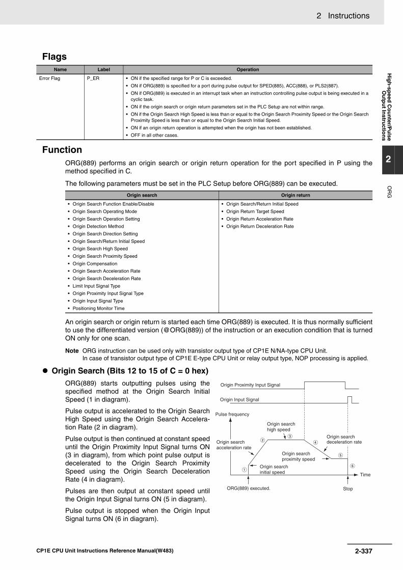
2 Instructions H
igh
-speed
Co
un
ter/Pu
lseO
utp
ut In
structio
ns
2
OR
G
Flags
FunctionORG(889) performs an origin search or origin return operation for the port specified in P using themethod specified in C.
The following parameters must be set in the PLC Setup before ORG(889) can be executed.
An origin search or origin return is started each time ORG(889) is executed. It is thus normally sufficientto use the differentiated version (@ORG(889)) of the instruction or an execution condition that is turnedON only for one scan.
Note ORG instruction can be used only with transistor output type of CP1E N/NA-type CPU Unit.In case of transistor output type of CP1E E-type CPU Unit or relay output type, NOP processing is applied.
Origin Search (Bits 12 to 15 of C = 0 hex)ORG(889) starts outputting pulses using thespecified method at the Origin Search InitialSpeed (1 in diagram).
Pulse output is accelerated to the Origin SearchHigh Speed using the Origin Search Accelera-tion Rate (2 in diagram).
Pulse output is then continued at constant speeduntil the Origin Proximity Input Signal turns ON(3 in diagram), from which point pulse output isdecelerated to the Origin Search ProximitySpeed using the Origin Search DecelerationRate (4 in diagram).
Pulses are then output at constant speed untilthe Origin Input Signal turns ON (5 in diagram).
Pulse output is stopped when the Origin InputSignal turns ON (6 in diagram).
Name Label Operation
Error Flag P_ER • ON if the specified range for P or C is exceeded.
• ON if ORG(889) is specified for a port during pulse output for SPED(885), ACC(888), or PLS2(887).
• ON if ORG(889) is executed in an interrupt task when an instruction controlling pulse output is being executed in a cyclic task.
• ON if the origin search or origin return parameters set in the PLC Setup are not within range.
• ON if the Origin Search High Speed is less than or equal to the Origin Search Proximity Speed or the Origin Search Proximity Speed is less than or equal to the Origin Search Initial Speed.
• ON if an origin return operation is attempted when the origin has not been established.
• OFF in all other cases.
Origin search Origin return
• Origin Search Function Enable/Disable
• Origin Search Operating Mode
• Origin Search Operation Setting
• Origin Detection Method
• Origin Search Direction Setting
• Origin Search/Return Initial Speed
• Origin Search High Speed
• Origin Search Proximity Speed
• Origin Compensation
• Origin Search Acceleration Rate
• Origin Search Deceleration Rate
• Limit Input Signal Type
• Origin Proximity Input Signal Type
• Origin Input Signal Type
• Positioning Monitor Time
• Origin Search/Return Initial Speed
• Origin Return Target Speed
• Origin Return Acceleration Rate
• Origin Return Deceleration Rate
Pulse frequency
Origin search initial speed
Origin search high speed
Origin search proximity speed
ORG(889) executed.
Origin Proximity Input Signal
Stop
Origin Input Signal
Time
Origin search acceleration rate
Origin search deceleration rate
2-337CP1E CPU Unit Instructions Reference Manual(W483)
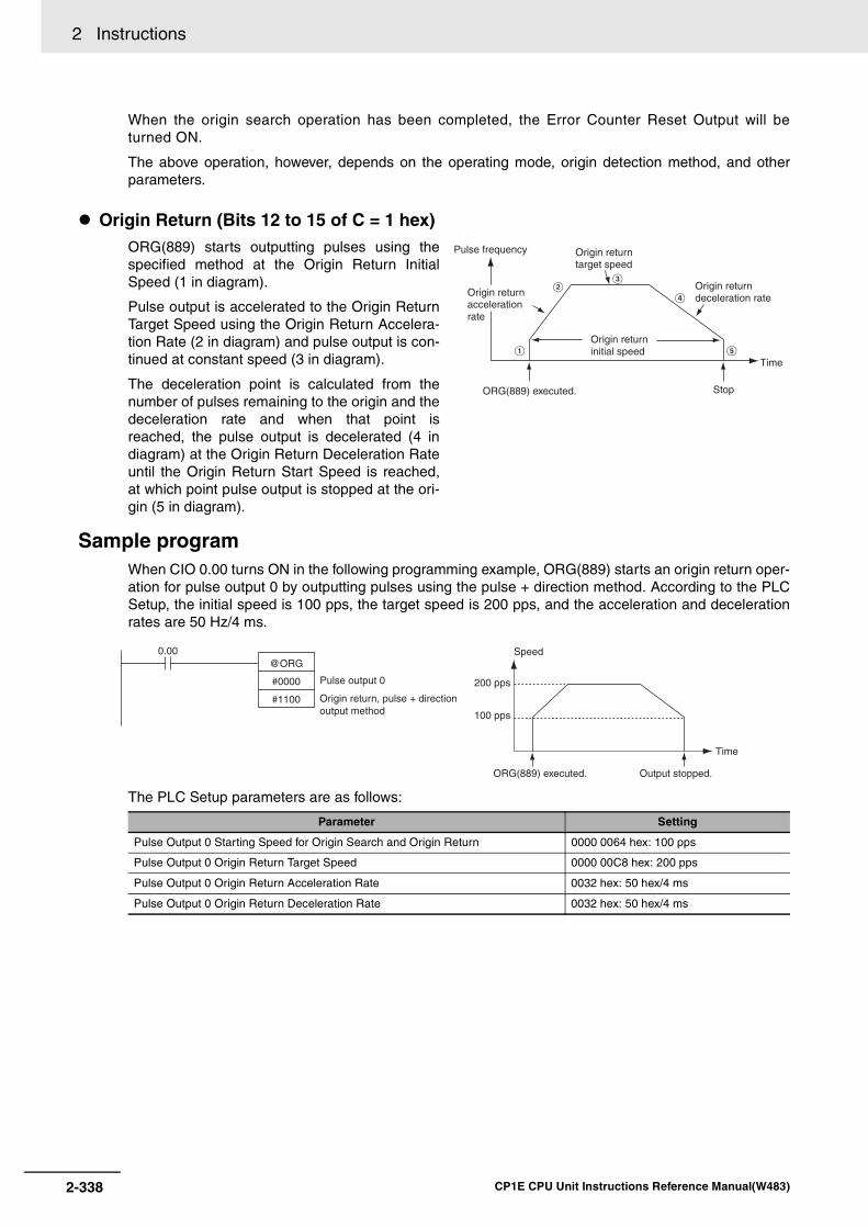
2 Instructions
When the origin search operation has been completed, the Error Counter Reset Output will beturned ON.
The above operation, however, depends on the operating mode, origin detection method, and otherparameters.
Origin Return (Bits 12 to 15 of C = 1 hex)ORG(889) starts outputting pulses using thespecified method at the Origin Return InitialSpeed (1 in diagram).
Pulse output is accelerated to the Origin ReturnTarget Speed using the Origin Return Accelera-tion Rate (2 in diagram) and pulse output is con-tinued at constant speed (3 in diagram).
The deceleration point is calculated from thenumber of pulses remaining to the origin and thedeceleration rate and when that point isreached, the pulse output is decelerated (4 indiagram) at the Origin Return Deceleration Rateuntil the Origin Return Start Speed is reached,at which point pulse output is stopped at the ori-gin (5 in diagram).
Sample programWhen CIO 0.00 turns ON in the following programming example, ORG(889) starts an origin return oper-ation for pulse output 0 by outputting pulses using the pulse + direction method. According to the PLCSetup, the initial speed is 100 pps, the target speed is 200 pps, and the acceleration and decelerationrates are 50 Hz/4 ms.
The PLC Setup parameters are as follows:
Parameter Setting
Pulse Output 0 Starting Speed for Origin Search and Origin Return 0000 0064 hex: 100 pps
Pulse Output 0 Origin Return Target Speed 0000 00C8 hex: 200 pps
Pulse Output 0 Origin Return Acceleration Rate 0032 hex: 50 hex/4 ms
Pulse Output 0 Origin Return Deceleration Rate 0032 hex: 50 hex/4 ms
Pulse frequency
ORG(889) executed.
Origin return target speed
Origin return deceleration rate
Stop
Time
Origin return initial speed
Origin return acceleration rate
@ORG
#0000
#1100
0.00
200 pps
100 pps
Pulse output 0
Origin return, pulse + directionoutput method
Time
Speed
ORG(889) executed. Output stopped.
2-338 CP1E CPU Unit Instructions Reference Manual(W483)
2 Instructions H
igh
-speed
Co
un
ter/Pu
lseO
utp
ut In
structio
ns
2
PW
M
PWM
Applicable Program Areas
Operands
P: Port Specifier
F: FrequencyF specifies the frequency of the PWM output between 2.0 and 6,553.5 Hz (0.1 Hz units, 0014 to FFFFhex), or between 2 and 32,000 Hz (2 Hz units, 0002 to 7D00 hex).
D: Duty Factor• 0.0% to 100.0% (0.1% units, 0000 to 03E8 hex)
D specifies the duty factor of the PWM output, i.e., the percentage of time that the output is ON.
Instruction Mnemonic VariationsFunction
codeFunction
PULSE WITH VARIABLE DUTY FACTOR
PWM @PWM 891PWM(891) is used to output pulses with the speci-fied duty factor from the specified port.
Symbol
PWM
Area Step program areas Subroutines Interrupt tasks
Usage OK OK OK
Operand Description Data type Size
P Port specifier --- 1
F Frequency --- 1
D Duty factor --- 1
P Port
1000 hex PWM output 0 (duty factor: in increments of 1%, frequency 0.1 Hz)
1100 hex PWM output 0 (duty factor: in increments of 1%, frequency 1 Hz)
P: Port specifier
F: Frequency
D: Duty factor
PWM
P
F
D
2-339CP1E CPU Unit Instructions Reference Manual(W483)

2 Instructions
Operand Specifications
Flags
FunctionPWM(891) outputs the frequency specified in F at the duty factor specified in D from the port specifiedin P. PWM(891) can be executed during duty-factor PWM output to change the duty factor without stop-ping PWM output. Any attempts to change the frequency will be ignored.
PWM output is started each time PWM(891) is executed. It is thus normally sufficient to use the differ-entiated version (@PWM(891)) of the instruction or an execution condition that is turned ON only forone scan.
The PWM output will continue either until INI(880) is executed to stop it (C = 0003 hex: stop PWM out-put) or until the CPU Unit is switched to PROGRAM mode.
Note PWM instruction can be used only with transistor output type of CP1E N/NA-type CPU Unit.In case of transistor output type of CP1E E-type CPU Unit or relay output type, NOP processing is applied.
Sample programWhen CIO 0.00 turns ON in the following programming example, PWM(891) starts PWM output fromPWM output 0 at 200 Hz with a duty factor of 50%. When CIO 0.01 turns ON, the duty factor is changedto 25%.
Area Word addresses Indirect DM addresses
Constants CF Pulse bits TR bitsCIO WR HR AR T C DM @DM *DM
P --- --- --- --- --- --- --- --- ---OK --- --- ---
F, D OK OK OK OK OK OK OK OK OK
Name Label Operation
Error Flag P_ER • ON if the specified range for P, F, or D is exceeded.
• ON if PWM are being output using ORG(889) for the specified port.
• ON if PWM(891) is executed in an interrupt task when an instruction controlling PWM output is being executed in a cyclic task.
• OFF in all other cases.
@PWM
#1000
#07D0
&500
0.00
@PWM
#1000
#07D0
&250
0.01
CIO 0.00 ON CIO 0.01 ON
PWM output 0
Frequency: 200.0 Hz
Duty factor: 50%
PWM output 0
Frequency: 200.0 Hz
Duty factor: 25%
Duty factor: 50% Duty factor: 25%
2-340 CP1E CPU Unit Instructions Reference Manual(W483)

2 Instructions S
tep In
structio
ns
2
Step Instructions
In CP1E series PLCs, STEP(008)/SNXT(009) can be used together to create step programs.
Note Work bits are used as the control bits for A, B, C and D.
Instruction Operation Diagram
SNXT(009): STEP START
Controls progression to the next step of the program. Step Ladder section start instruction
STEP(008): STEP DEFINE
Indicates the start of a step. Repeats the same step pro-gram until the conditions for progression to the next step are established.
Step Ladder section start instruction
Equivalent to
Step
Equivalent to
STEP
A
aSNXT
A
STEP
B
bSNXT
B
STEP
C
cSNXT
C
STEP
dSNXT
D
a
b
c
d
Process A
Process B
Process C
End
Corresponds
Process A
Process B
Process C
a turns ON
Starts the step programming area
Proceeds to the next step
Process A repeated until b turns ON.
b turns ON
Process B repeated until c turns ON.
c turns ON
Process C repeated until d turns ON.
Proceeds to the end of the ladder step programming area
d turns ON
Step programming area completed
2-341CP1E CPU Unit Instructions Reference Manual(W483)

2 Instructions
SNXT/STEP
Applicable Program Areas
Operands
Operand Specifications
Flags
Function SNXT(009)
SNXT(009) is used in the following three ways:1.To start step programming execution.2. To proceed to the next step control bit.3. To end step programming execution.
The step program area is from the first STEP(008) instruction (which always takes a control bit) to thelast STEP(008) instruction (which never takes a control bit).
Starting Step ExecutionSNXT(009) is placed at the beginning of the step program area to start step execution. It turns ONthe control bit specified for B for the next STEP(008) and proceeds to step B (all instructions afterSTEP(008) B). A differentiated execution condition must be used for the SNXT(009) instruction thatstarts step programming area execution, or step execution will last for only one cycle.
Instruction Mnemonic VariationsFunction
codeFunction
STEP START SNXT --- 009SNXT(009) is used to control progression of step execution in the step program area.
STEP DEFINE STEP --- 008STEP(008) is used to define the beginning and the end of the step program area.
Symbol
SNXT STEP
When defining the beginning of a step, a control bit is specified as follows:
When defining the end of a step, a control bit is not specified as follows:
Area Step program areas Subroutines Interrupt tasks
Usage OK Not allowed Not allowed
Operand Description Data type Size
B Bit --- 1
Area Word addresses Indirect DM addresses
Constants CF Pulse bits TR bitsCIO WR HR AR T C DM @DM *DM
B --- OK --- --- --- --- --- --- --- --- --- --- ---
Name Label Operation
SNXT STEP
Error Flag P_ER • ON when the specified bit B is not in the WR area.
• ON when SNXT(009) is used in an interrupt pro-gram.
• OFF in all other cases.
• ON when the specified bit B is not in the WR area.
• ON when STEP(008) is used in an interrupt pro-gram.
• OFF in all other cases.
B: Bit
SNXT(009)
BB: Bit
STEP(008)
B
STEP(008)
2-342 CP1E CPU Unit Instructions Reference Manual(W483)

2 Instructions S
tep In
structio
ns
2
SN
XT
/ST
EP
Proceeding to the Next StepWhen SNXT(009) occurs in the middle of the step program area, it is used to proceed to the nextstep. It turns OFF the previous control bit and turns ON the next control bit B, for the next step,thereby starting step B (all instructions after STEP(008) B).
Ending the Step Programming AreaWhen SNXT(009) is placed at the very end of the step program area, it ends step execution andturns OFF the previous control bit. The control bit specified for B is a dummy bit. This bit will howeverbe turned ON, so be sure to select a bit that will not cause problems.
STEP(008)STEP(008) functions in following 2 ways, depending on its position and whether or not a control bit hasbeen specified.1. Starts a specific step.2. Ends the step program area (i.e., step execution).
Starting a StepSTEP(008) is placed at the beginning of each step with an operand, B, that serves as the control bitfor the step.
The control bit B will be turned ON by SNXT(009) and the instruction in the step will be executedfrom the one immediately following STEP(008). A200.12 (Step Flag) will also turn ON when execu-tion of a step begins.
After the first cycle, step execution will continue until the conditions for changing the step are estab-lished, i.e., until the SNXT(009) instruction turns ON the control bit in the next STEP(008).
When SNXT (009) turns ON the control bit for a step, the control bit B of the current instruction willbe reset (turned OFF) and the step controlled by bit B will become interlocked.
Handling of outputs and instructions in a step will change according to the ON/OFF status of thecontrol bit B. (The status of the control bit is controlled by SNXT(009)). When control bit B is turnedOFF, the instructions in the step are reset and are interlocked. Refer to the following tables.
Interlock Status (IL)
Note Indicates all other instructions, such as TTIM(087), TTIMX(555), SET, REST, CNT, CNTX(546),CNTR(012), CNTRX(548), SFT(010), and KEEP(011).
The STEP(008) instruction must be placed at the beginning of each step. STEP(008) is placed atthe beginning of a step area to define the start of the step.
Ending the Step Program Area STEP(008) is placed at the end of the step program area without an operand to define the end ofstep programming.
When the control bit preceding a SNXT(009) instruction is turned OFF, step execute is stopped bySNXT(009).
Control bit status Handling
ON Instructions in the step are executed normally.
ON→OFF Bits and instructions in the step are interlocked as shown in the next table.
OFF All instructions in the step are processed as NOPs.
Instruction output Status
Bits specified for OUT, OUT NOT All OFF
TIM, TIMX(551), TIMH(015), TIMHX(551), TMHH(540), TIMHHX(552), TIML(542), and TIMLX(553)
PV 0000 hex (reset)
Completion Flag OFF (reset)
Bits or words specified for other instructions (see note) Holds the previous status (but the instructions are not executed)
2-343CP1E CPU Unit Instructions Reference Manual(W483)

2 Instructions
Hint
Related Bits
Precaution• The control bit, B, must be in the Work Area for STEP(008)/SNXT(009).
• A control bit for STEP(008)/SNXT(009) cannot be use anywhere else in the ladder diagram. If thesame bit is used twice, as duplication bit error will occur.
• If SBS(091) is used to call a subroutine from within a step, the subroutine outputs and instructions willnot be interlocked when the control bit turns OFF.
• SNXT(009) will be executed when the execution condition is ON.
• Input SNXT(009) at the end of the step program area and make sure that the control bit is a dummybit in the Work Area. If a control bit for a step is used in the last SNXT(009) in the step program area,the corresponding step will be started when SNXT(009) is executed.
A200.12 (Step Flag) is turned ON for one cyclewhen STEP(008) is executed. This flag can beused to conduct initialization once the step exe-cution has started.
Name Address Details
Step Flag A200.12 ON for one cycle when a step program is started using STEP(008). Can be used to reset timers and perform other processing when starting a new step.
1 cycle
Start
CNT
0001
#0003
STEP
W0.00
SNXT
W0.00
0.01
0.00
A200.12
W0.00
A200.12
Step a starts when C turns ON
A executed
When d turns ON, b starts (A is interlocked)
B executed
e turns ON (B is interlocked)
End of step programming area
Normal ladder program Returns to normal ladder program
STEP
a
cSNXT
a
A
STEP
b
dSNXT
b
B
STEP
eSNXT
(Dummy)
2-344 CP1E CPU Unit Instructions Reference Manual(W483)

2 Instructions S
tep In
structio
ns
2
SN
XT
/ST
EP
• STEP(008) and SNXT(009) cannot be used inside of subroutines, interrupt programs, or block pro-grams.
• Be sure that two steps are not executed during the same cycle.
• The instructions that cannot be used within step programs are listed in the following table.
Sample program
Function Mnemonic Name
Sequence Control Instructions END(001) END
IL(002) INTERLOCK
ILC(003) INTERLOCK CLEAR
JMP(004) JUMP
JME(005) JUMP END
CJP(510) CONDITIONAL JUMP
Subroutine Instructions SBN(092) SUBROUTINE ENTRY
RET(093) SUBROUTINE RETURN
Step (A) ladder program
Step (B) ladder program
Normal ladder program
CIO 0.00 turns ON, step W0.00 starts
Step W0.00 starts from the next instruction
Step W0.00
W0.00 turns OFF, W0.01 turns ON and step W0.01 starts
Step W0.01 starts from the next instruction
W0.01 turns OFF and dummy bit W30.0 turns ON
End of step programming area
Step W0.01
End of step program
ming area
STEP
W0.00
0.00SNXT
W0.00
STEP
W0.01
0.01SNXT
W0.01
STEP
0.02SNXT
W30.0
2-345CP1E CPU Unit Instructions Reference Manual(W483)
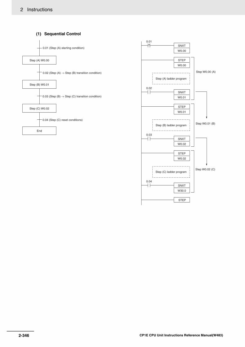
2 Instructions
(1) Sequential Control
Step (A) W0.00
Step (B) W0.01
Step (C) W0.02
End
0.01 (Step (A) starting condition)
0.02 (Step (A) → Step (B) transition condition)
0.03 (Step (B) → Step (C) transition condition)
0.04 (Step (C) reset conditions)
Step W0.00 (A)
Step W0.01 (B)
Step W0.02 (C)Step (C) ladder program
Step (B) ladder program
Step (A) ladder program
STEP
W0.00
SNXT
W0.00
STEP
W0.01
SNXT
W0.01
SNXT
W0.02
STEP
W0.02
STEP
0.01
0.02
0.03
0.04
SNXT
W30.0
2-346 CP1E CPU Unit Instructions Reference Manual(W483)

2 Instructions S
tep In
structio
ns
2
SN
XT
/ST
EP
(2) Branching Control
Additional Information:• In the above example, where SNXT(009) is executed for W0.02, the branching moves onto the next
steps even though the same control bit is used twice. This is not picked up as an error in the programcheck using the CX-Programmer. A duplicate bit error will only occur in a step ladder program onlywhen a control bit in a step instructions is also used in the normal ladder diagram.
• The above programming is used when steps A and B cannot be executed simultaneously. For simul-taneous execution of A and B, delete the execution conditions illustrated below.
Step (A) W0.00 Step (B) W0.01
Step (C) W0.02
End
0.05 (Step (C) reset conditions)
0.01 (Step (A) starting condition)
0.02 (Step (B) starting condition)
0.03 (Step (A) → Step (C) transition condition)
0.04 (Step (B) → Step (C) transition condition) STEP
W0.00
0.02
SNXT
W0.01
0.01
SNXT
W0.00
0.01
0.02
STEP
W0.01
0.03
SNXT
W0.02
0.04
SNXT
W0.02
STEP
W0.02
STEP
0.05
SNXT
W30.0
Step (A) ladder program
Step (B) ladder program
Step (C) ladder program
Step W0.00 (A)
Step W0.01 (B)
Step W0.02 (C)
0.02 0.01
2-347CP1E CPU Unit Instructions Reference Manual(W483)
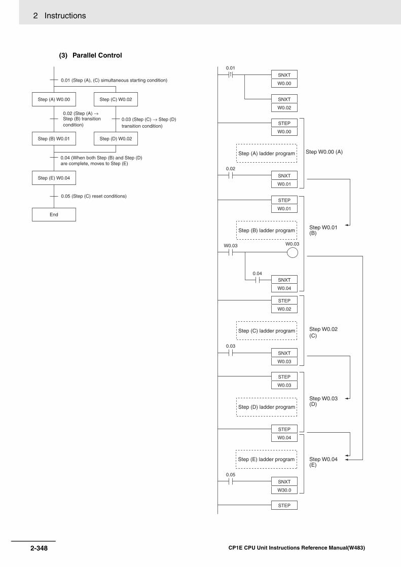
2 Instructions
(3) Parallel Control
Step (A) W0.00
Step (B) W0.01
Step (C) W0.02
End
0.05 (Step (C) reset conditions)
Step (D) W0.02
Step (E) W0.04
0.04 (When both Step (B) and Step (D) are complete, moves to Step (E)
0.03 (Step (C) → Step (D) transition condition)
0.01 (Step (A), (C) simultaneous starting condition)
0.02 (Step (A) → Step (B) transition condition)
STEP
W0.01
SNXT
W0.02
0.01
SNXT
W0.00
STEP
W0.02
W0.03
0.04
W0.03
0.03
SNXT
W0.03
STEP
W0.00
0.02
SNXT
W0.01
STEP
W0.03
STEP
W0.04
STEP
0.05
SNXT
W0.04
SNXT
W30.0
Step (A) ladder program Step W0.00 (A)
Step W0.01 (B)Step (B) ladder program
Step W0.02 (C)
Step (C) ladder program
Step W0.03 (D)Step (D) ladder program
Step W0.04 (E)
Step (E) ladder program
2-348 CP1E CPU Unit Instructions Reference Manual(W483)

2 Instructions S
tep In
structio
ns
2
SN
XT
/ST
EP
Application Examples(1) Sequential Execution
SW 1
SW 2SW 3
SW 4
Solenoid 1 Robot hand
Solenoid 2
Conveyor belt 1
Process A: Loading
Conveyor belt 2
Process B: Part installation
Conveyor belt 3
Process C: Inspection/Unloading
Photomicro-sensor
0.01 (SW1)
0.02 (SW2)
0.03 (SW3)
0.04 (SW4)
Process A
Process B
Process C
Loading
End
Part Installation
Inspection/Unloading
Explanation of operation(1) SW1 ON: Solenoid 1 operates Conveyor 1 operates(2) SW2 ON stops the previous process Robot hand operates Conveyor 2 operates(3) SW3 ON stops the previous process Photo microsensor operates (for part inspection) Conveyor 3 operates Solenoid 2 operates (removal of defective items)(4) SW4 ON stops the previous process
Additional InformationWhen another process is started from within a process (when an SNXT instruction turns ON), all outputs of the current process are turned OFF within that cycle.
Process A
Process B
Process C
Process A started.
Process A reset. Process B started.
Process B reset. Process C started.
Process C reset.
Programming for process A
Programming for process B
Programming for process C
0.01(SW1)
0.01(SW1)
0.02(SW2)
0.03(SW3)
STEP
W0.00
SNXT
W0.00
STEP
W0.01
SNXT
W0.01
SNXT
W0.02
STEP
W0.02
STEP
SNXT
W30.0
2-349CP1E CPU Unit Instructions Reference Manual(W483)
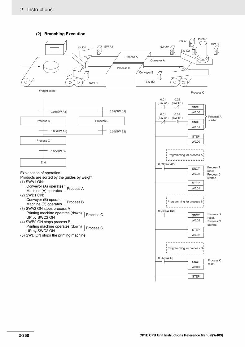
2 Instructions
(2) Branching Execution
SW A1 SW A2
SW C1
SW C2
SW D
SW B2SW B1
Process C
Process B
Process A
Guide
Weight scale
Conveyer B
Conveyer A
Printer
0.01(SW A1) 0.02(SW B1)
0.03(SW A2) 0.04(SW B2)
0.05(SW D)
Process A
Process C
End
Process B
Explanation of operationProducts are sorted by the guides by weight.(1) SWA1 ON: Conveyor (A) operates Machine (A) operates(2) SWB1 ON: Conveyor (B) operates Machine (B) operates(3) SWA2 ON stops process A Printing machine operates (down) UP by SWC2 ON(4) SWB2 ON stops process B Printing machine operates (down) UP by SWC2 ON(5) SWD ON stops the printing machine
Process A
Process B
Process C
Process C
Process C reset.
Process B reset. Process C started.
Process A reset. Process C started.
Process A started.
Programming for process C
Programming for process B
Programming for process A
STEP
W0.00
0.01(SW A1)
SNXT
W0.01
0.01(SW A1)
SNXT
W0.000.02
(SW B1)
0.02(SW B1)
STEP
W0.01
0.03(SW A2)
SNXT
W0.02
0.04(SW B2)
SNXT
W0.02
STEP
W0.02
STEP
0.05(SW D)SNXT
W30.0
2-350 CP1E CPU Unit Instructions Reference Manual(W483)

2 Instructions S
tep In
structio
ns
2
SN
XT
/ST
EP
(3) Parallel Execution
SW1
SW2
SW3
SW4 SW6
SW5 SW7
Process C
Process A
Process D
Process B
Process E
Conveyer A
Conveyer C Conveyer D
Conveyer B
Conveyer E
0.05(SW7)
0.02(SW3) 0.03(SW4)
Process A
Process E
End
Process C
Process B Process D
0.04(SW5 and SW6 both ON)
0.01(SW 1 and SW2 both ON)
Explanation of operation(1) SW1, SW2 ON: Conveyor (A) operates
Work (A) operates Conveyor (C) operates
Work (C) operates(2) SW3 ON: Process (A) stops Conveyor (B) operates
Work (B) operates(3) SW4 ON: Process (C) stops Conveyor (D) operates
Work (D) operates(4) SW5, SW6 ON: Process (B) stops Process (D) stops Conveyor (E) operates
Work (E) operates(5) SW7 ON: Process (E) stops
Additional InformationThe STEP instruction turns all outputs in its process OFF when ON changes to OFF.
Process A
Process C
Process B
Process D
Process E
Note When processes (B) and (D) are in operation and SW5 and SW6 turn ON, it is judged that processes (B) and (D) are finished.Execution of SNXT W0.04 turns OFF the outputs of process (B) and W0.03 turns OFF.STEP W0.03 judges ON to OFF and turns OFF the outputs of process (D).
Process A started.
Process C started.
Programming for process A
Process A reset.
Process B started.
Used to turn off process D.
Process E started.
Programming for process C
Process C reset.
Process D started.
Programming for process D
Programming for process E
Process E reset.
Programming for process B
W0.03
0.04(SW5, SW6)
0.01(SW1, SW2)
0.02(SW3)
0.03(SW4)
0.05(SW7)
W0.04
STEP
W0.01
SNXT
W0.02
SNXT
W0.00
STEP
W0.02
SNXT
W0.04
SNXT
W0.03
STEP
W0.00
SNXT
W0.01
STEP
W0.03
STEP
W0.04
STEP
SNXT
W30.0
W0.03
2-351CP1E CPU Unit Instructions Reference Manual(W483)
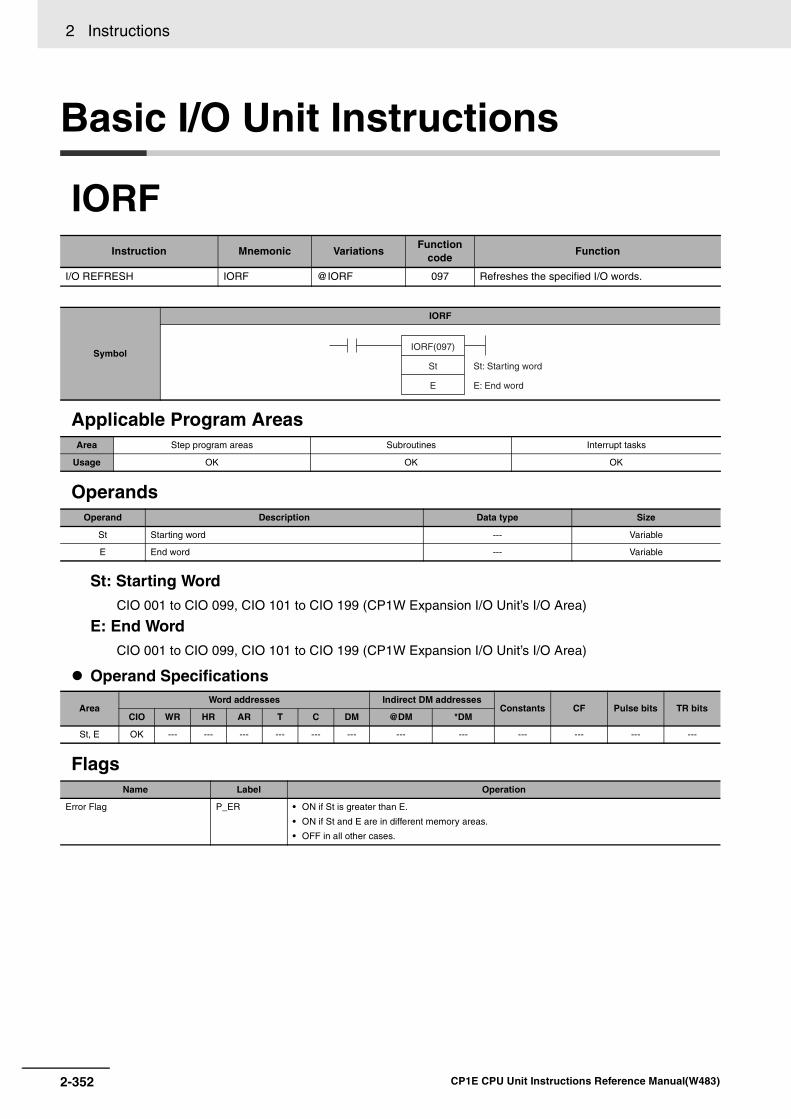
2 Instructions
Basic I/O Unit Instructions
IORF
Applicable Program Areas
Operands
St: Starting WordCIO 001 to CIO 099, CIO 101 to CIO 199 (CP1W Expansion I/O Unit’s I/O Area)
E: End WordCIO 001 to CIO 099, CIO 101 to CIO 199 (CP1W Expansion I/O Unit’s I/O Area)
Operand Specifications
Flags
Instruction Mnemonic VariationsFunction
codeFunction
I/O REFRESH IORF @IORF 097 Refreshes the specified I/O words.
Symbol
IORF
Area Step program areas Subroutines Interrupt tasks
Usage OK OK OK
Operand Description Data type Size
St Starting word --- Variable
E End word --- Variable
Area Word addresses Indirect DM addresses
Constants CF Pulse bits TR bitsCIO WR HR AR T C DM @DM *DM
St, E OK --- --- --- --- --- --- --- --- --- --- --- ---
Name Label Operation
Error Flag P_ER • ON if St is greater than E.
• ON if St and E are in different memory areas.
• OFF in all other cases.
St: Starting word
E: End word
IORF(097)
St
E
2-352 CP1E CPU Unit Instructions Reference Manual(W483)

2 Instructions B
asic I/O U
nit In
structio
ns
2
IOR
F
Units Refreshed by IORF(097)
Note CP1E CPU Unit built-in I/O area cannot be refreshed with IORF(097).CP1E CPU Unit built-in I/O area can be refreshed with immediate refreshing specifications (!).
Function
Precaution• IORF(097) can be used in an interrupt task, which allows high-speed processing of specific I/O data
with an interrupt. If IORF(097) is used in an interrupt task, always disable cyclic refreshing of thespecified Special I/O Unit by turning ON the corresponding Special I/O Unit Cyclic Refreshing Dis-able Bit in the PLC Setup.
• If words for which there is no Unit mounted exist between St and E, nothing will be done for thosewords and only the words allocated to Units will be refreshed.
• The I/O refreshing initiated by IORF(097) will be stopped midway if an I/O bus error occurs during I/Orefreshing.
Sample program
Refreshing Words in the I/O Bit AreaWhen CIO 0.00 turns ON in the following example, CIO 2 to CIO 4 (36 inputs) are refreshed (1) andthen after the required processing is performed (2), CIO 104 (8 outputs) is refreshed (3).
Unit type CH Refreshable by IORF(097)
CPU Unit with 30 or 40 I/O Points
CP1E CPU Unit built-in I/O: 0CH, 1CH, 100CH and 101CH No
CP1W Expansion I/O Unit: 2CH to 99CH, 102CH to 199CH Yes
CP1W Expansion Unit: 2CH to 99CH, 102CH to 199CH Yes
CPU Unit with 60 I/O Points
CP1E CPU Unit built-in I/O: 0CH, 1CH, 2CH, 100CH, 101CH and 102CH No
CP1W Expansion I/O Unit: 3CH to 99CH, 103CH to 199CH Yes
CP1W Expansion Unit: 3CH to 99CH, 103CH to 199CH Yes
NA-type CPU Unit
CP1E CPU Unit built-in I/O: 0CH and 100CH No
CP1E CPU Unit built-in analog: 90CH, 91CH and 190CH Yes
CP1W Expansion I/O Unit: 1CH to 99CH, 101CH to 199CH Yes
CP1W Expansion Unit: 1CH to 99CH, 101CH to 199CH Yes
IORF(097) refreshes the I/O words between St and E,inclusively. IORF(097) is used to refresh words allo-cated to CP1W Expansion (I/O) Units. For 30 or 40 I/OPoints, Expansion (I/O) Units are allocated wordsbetween CIO 002 and CIO 099, CIO102 and CIO199.For 60 I/O Points, Expansion (I/O) Units are allocatedwords between CIO 003 and CIO 099, CIO103 andCIO199. For NA20 I/O Points, Expansion (I/O) Unitsare allocated words between CIO 001 and CIO 099,CIO101 and CIO199.
St
E
I/O refreshing
I/O bit areaCP1W Expansion Units, CP1W Expansion I/O Units
IORF
2
4
0.00
St
E
StE
IORF
104
104
St
E
015
015
St CIO 2 CIO 3
E CIO 4
CIO 104
CIO 2 and CIO 3
CIO 102 and CIO 103
CIO 4
CIO 104
(1)
(2)
(3) I/O refreshing
ProcessingCPM1A Expansion I/O Units
2-353CP1E CPU Unit Instructions Reference Manual(W483)

2 Instructions
SDEC
Applicable Program Areas
Operands
Di: Digit designator
Operand Specifications
Flags
Instruction Mnemonic VariationsFunction
codeFunction
7-SEGMENT DECODER SDEC @SDEC 078
Converts the hexadecimal contents of the desig-nated digit(s) into 8-bit, 7-segment display code and places it into the upper or lower 8-bits of the specified destination words.
Symbol
SDEC
Area Step program areas Subroutines Interrupt tasks
Usage OK OK OK
Operand Description Data type Size
S Source word UINT 1
Di Digit designator UINT 1
D First destination word UINT Variable
Area Word addresses Indirect DM addresses
Constants CF Pulse bits TR bitsCIO WR HR AR T C DM @DM *DM
S
OK OK OK OK OK OK OK OK OK
---
--- --- ---Di OK
D ---
Name Label Operation
Error Flag P_ER • ON if settings in Di are not within the specified ranges.
• OFF in all other cases.
S: Source word
Di: Digit designator
D: First destination word
SDEC(078)
S
Di
D
0 1/0 m n
15 12 11 8 7 4 3 0
Di
First digit of S to convert (0 to 3)0: Digit 0 (bits 0 to 3 of S) 1: Digit 1 (bits 4 to 7 of S) 2: Digit 2 (bits 8 to 11 of S) 3: Digit 3 (bits 12 to 15 of S)
Number of digits to convert
0 to 3: 1 to 4 digits
First half of D to receive converted data0: Rightmost 8 bits (1st half) 1: Leftmost 8 bits (2nd half)
Not used; set to 0.
2-354 CP1E CPU Unit Instructions Reference Manual(W483)

2 Instructions B
asic I/O U
nit In
structio
ns
2
SD
EC
Function
Precaution• If more than one digit is specified for conversion in Di, digits are converted in order toward the most-
significant digit. Digit 0 is the next digit after digit 3.
• Results are stored in D in order from the specified portion toward higher-address words. If just one ofthe bytes in a destination word receives converted data, the other byte is left unchanged.
Sample programWhen CIO 0.00 turns ON in the following example, the contents of the 3 digits beginning with digit 1 inD100 will be converted from hexadecimal data to 7-segment data, and the results will be output to theupper byte of D200 and both bytes of D201. The specifications of the bytes to be converted and thelocation of the output bytes are made in CIO 100.
SDEC(078) regards the data specified byS as 4-digit hexadecimal data, converts thedigits specified in S by Di (first digit andnumber of digits) to 7-segment data andoutputs the results to D in the bits specifiedin Di.
Number of digits
Rightmost 8 bits (0)
7-segment
First digit to convertSS+1
n
m
DD+1D+2
Di 0 1/08111215
m n0347
HEX
SDEC
D100
100
D200
0.00
S
Di
D
8111215
3 2 1 0
0347
18111215
2 1 F
1
7 15 B 0 6
0347
Hexadecimal to 7-segment data conversion (F → 71, 1 → 06, and 2 → 5B)
S: D100
Di: 100 3
D: D200
D201
2-355CP1E CPU Unit Instructions Reference Manual(W483)
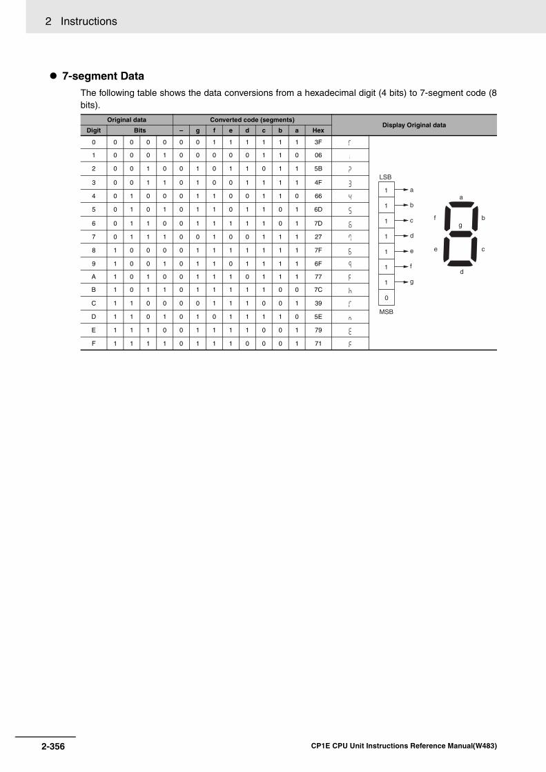
2 Instructions
7-segment DataThe following table shows the data conversions from a hexadecimal digit (4 bits) to 7-segment code (8bits).
Original data Converted code (segments)Display Original data
Digit Bits – g f e d c b a Hex
0 0 0 0 0 0 0 1 1 1 1 1 1 3F
1 0 0 0 1 0 0 0 0 0 1 1 0 06
2 0 0 1 0 0 1 0 1 1 0 1 1 5B
3 0 0 1 1 0 1 0 0 1 1 1 1 4F
4 0 1 0 0 0 1 1 0 0 1 1 0 66
5 0 1 0 1 0 1 1 0 1 1 0 1 6D
6 0 1 1 0 0 1 1 1 1 1 0 1 7D
7 0 1 1 1 0 0 1 0 0 1 1 1 27
8 1 0 0 0 0 1 1 1 1 1 1 1 7F
9 1 0 0 1 0 1 1 0 1 1 1 1 6F
A 1 0 1 0 0 1 1 1 0 1 1 1 77
B 1 0 1 1 0 1 1 1 1 1 0 0 7C
C 1 1 0 0 0 0 1 1 1 0 0 1 39
D 1 1 0 1 0 1 0 1 1 1 1 0 5E
E 1 1 1 0 0 1 1 1 1 0 0 1 79
F 1 1 1 1 0 1 1 1 0 0 0 1 71
1
1
1
1
1
1
1
0
g
c
d
e
bf
aa
b
c
d
e
f
g
LSB
MSB
2-356 CP1E CPU Unit Instructions Reference Manual(W483)

2 Instructions B
asic I/O U
nit In
structio
ns
2
DS
W
DSW
Applicable Program Areas
Operands
I: Input Word (Data Line D0 to D3 Inputs)Specify the input word allocated to the Input Unit and connect the digital switch’s D0 to D3 data lines tothe Input Unit as shown in the following diagram.
O: Output Word (CS/RD Control Signal Outputs)Specify the output word allocated to the Output Unit and connect the digital switch’s control signals (CSand RD signals) to the Output Unit as shown in the following diagram.
Instruction Mnemonic VariationsFunction
codeFunction
DIGITAL SWITCH INPUT DSW --- 210
Reads the value set on a external digital switch (or thumbwheel switch) connected to an I/O Unit and stores the 4-digit or 8-digit value in the specified words.
Symbol
DSW
Area Step program areas Subroutines Interrupt tasks
Usage OK OK Not allowed
Operand Description Data type Size
I Input word UINT 1
O Output word UINT 1
D First result word WORD Variable
C1 Number of digit UINT 1
C2 System word WORD 1
I: Input word
O: Output word
D: First result word
C1: Number of digits
C2: System word
DSW(210)
I
O
D
C1
C2
0123456789101112131415
I
D0D1D2D3
D3D2D1D0
Rightmost 4 digitsLeftmost 4 digits
0123456789101112131415
O
CS0CS1CS2CS3
CS signalsOne Round FlagRD0 Read signal
2-357CP1E CPU Unit Instructions Reference Manual(W483)

2 Instructions
D: First Result WordSpecifies the leading word address where the external digital switch’s set values will be stored.
C1: Number of DigitsSpecifies the number of digits that will be read from the external digital switch. Set C1 to 0000 hex toread 4 digits or 0001 hex to read 8 digits.
C2: System WordSpecifies a work word used by the instruction. This word cannot be used in any other application.
Operand Specifications
Flags
FunctionDSW(210) outputs control signals to bits 00 to 04 of O, reads the specified number of digits (either 4-digit or 8-digit, specified in C1) of digital switch data line data from I, and stores the result in D and D+1.(If 4 digits are read, the result is stored in D. If 8 digits are read, the result is stored in D and D+1.)
DSW(210) reads the 4-digit or 8-digit switch data once every 16 cycles, and then starts over and contin-ues reading the data. The One Round Flag (bit 05 of O) is turned ON once every 16 CPU Unit cycles.
Area Word addresses Indirect DM addresses
Constants CF Pulse bits TR bitsCIO WR HR AR T C DM @DM *DM
I, O, D OK OK OK OK OK OK OK OK OK ---
--- --- ---C1 --- --- --- --- --- --- --- ------
OK
C2 OK OK OK OK OK OK OK OK ---
Name Label Operation
Error Flag P_ER OFF
D
815 12 11 0347
D+1
815 12 11 0347
Digit 1Digit 2Digit 3Digit 4
Digit 5Digit 6Digit 7Digit 8
Note: Only when C1 = 0001 hex to read 8 digits.
(See note.)
C2
15 0
System word(Cannot be accessed by the user.)
2-358 CP1E CPU Unit Instructions Reference Manual(W483)

2 Instructions B
asic I/O U
nit In
structio
ns
2
DS
W
External ConnectionsConnect the digital switch or thumbwheel switch to Input Unit contacts 0 to 7 and Output Unit contacts 0to 4, as shown in the following diagram. The following example illustrates connections for an A7B Thum-bwheel Switch.
Timing Chart
CO
M
00
01
02
03
04
05
06
07
08
09
10
11
IN
CP1W-20EDT
OUT
CO
M
00
CO
M
01
CO
M
02
03
CO
M
04
05
06
07
8
No. 1No. 2No. 3No. 4No. 5No. 6No. 7No. 8
4 2 1
A7B Thumbwheel Switch
Switch Switch Switch Switch Switch Switch Switch Switch
00
01
02
03
04
05
O
10 0 10 1 10 2 10 3
D+1 D
0 1 2 3 4 5 6 7 8 9 10 11 12 13 14 15 16
I
Leftmost 4 digits
Rightmost 4 digits
Input data
CS signals
One Round Flag
RD (read) signal
16 cycles to complete one round of execution
Eight digits: 00 to 03, 04 to 07
Four digits: 00 to 03
When only 4 digits are read, only word D is used.
2-359CP1E CPU Unit Instructions Reference Manual(W483)

2 Instructions
Precaution• Do not read or write the system word (C2) from any other instruction. DSW(210) will not operate cor-
rectly if the system word is accessed by another instruction. The system word is not initialized byDSW(210) in the first cycle when program execution starts. If DSW(210) is being used from the firstcycle, clear the system word from the program.
• DSW(210) will not operate correctly if I/O refreshing is not performed with the Input Unit and OutputUnit connected to the digital switch or thumbwheel switch after DSW(210) is executed. Consequently,set the input time constant for the Input Units used for the data line input word to a value that isshorter than the cycle time.
• DSW(210) reads the 4-digit or 8-digit data once in 16 cycles, and then starts over and reads the dataagain in the next 16 cycles.
• When executed, DSW(210) begins reading the switch data from the first of the sixteen cycles, regard-less of the point at which the last instruction was stopped.
Sample programIn this example, DSW(210) is used to read an 8-digit number from a digital switch and outputs theresulting value constantly to D0 and D3. The digital switch is connected through CIO 3 and CIO 104.
D1000 is used as the system word.
I
O
D
C1
C2
DSW(210)
3
104
D0
#0001
D1000
P_On
Always ON Flag
2-360 CP1E CPU Unit Instructions Reference Manual(W483)

2 Instructions B
asic I/O U
nit In
structio
ns
2
MT
R
MTR
Applicable Program Areas
Operands
I: Input WordSpecify the input word allocated to the Input Unit and connect the 8 input signal lines to the Input Unitas shown in the following diagram.
O: Output Word (Selection Signal Outputs)Specify the output word allocated to the Output Unit and connect the 8 selection signals to the OutputUnit as shown in the following diagram.
Instruction Mnemonic VariationsFunction
codeFunction
MATRIX INPUT MTR --- 213
Inputs up to 64 signals from an 8 × 8 matrix con-nected to an Input Unit and an Output Unit (using 8 input points and 8 output points) and stores that 64-bit data in the 4 destination words.
Symbol
MTR
Area Step program areas Subroutines Interrupt tasks
Usage OK OK Not allowed
Operand Description Data type Size
I Input word UINT 1
O Output word UINT 1
D First destination word ULINT 4
C System word WORD 1
I: Input word
O: Output word
D: First destination word
C: System word
MTR(213)
I
O
D
C
0123456789101112131415
I
01234567
Bits 00 to 07 correspond to Input Unit inputs 0 to 7.
0123456789101112131415
O
01234567
Bits 00 to 07 correspond to Output Unit outputs 0 to 7.
2-361CP1E CPU Unit Instructions Reference Manual(W483)
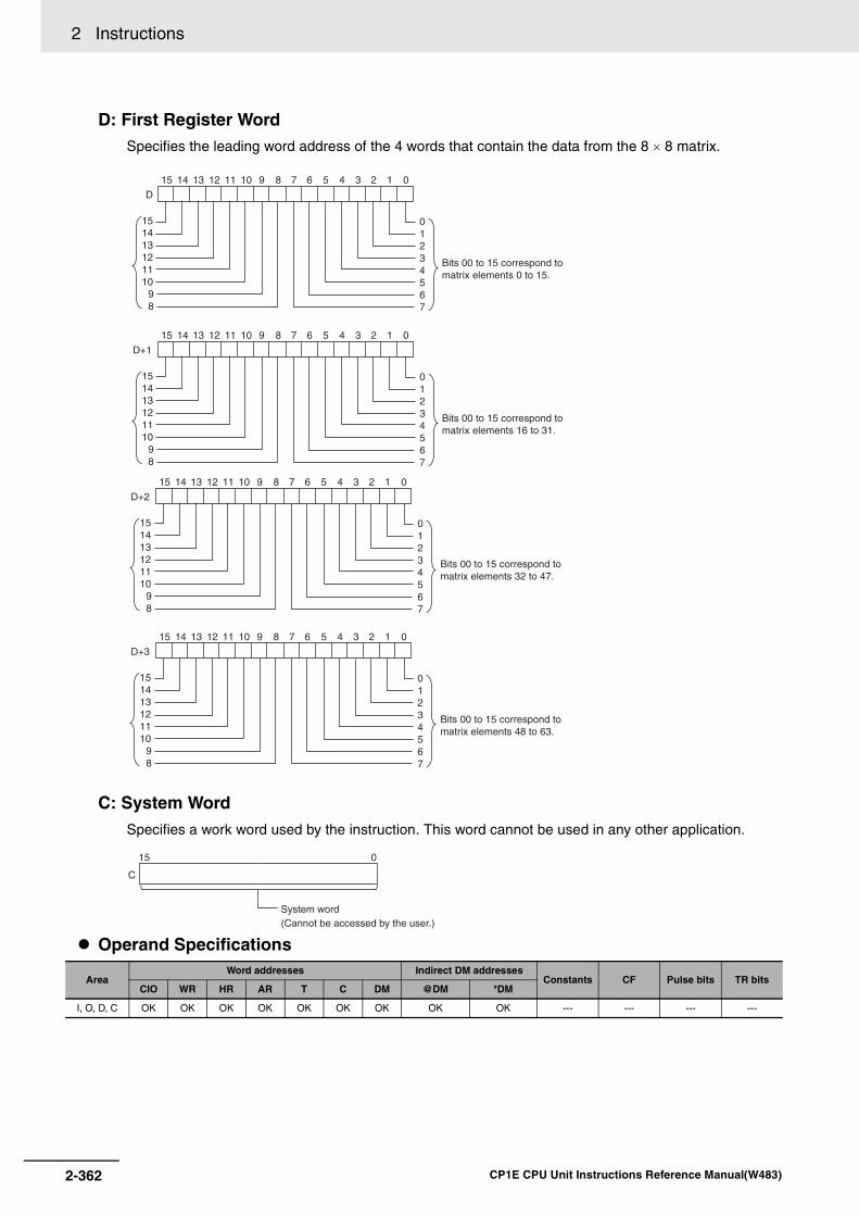
2 Instructions
D: First Register WordSpecifies the leading word address of the 4 words that contain the data from the 8 × 8 matrix.
C: System WordSpecifies a work word used by the instruction. This word cannot be used in any other application.
Operand Specifications
Area Word addresses Indirect DM addresses
Constants CF Pulse bits TR bitsCIO WR HR AR T C DM @DM *DM
I, O, D, C OK OK OK OK OK OK OK OK OK --- --- --- ---
0123456789101112131415
D
01234567
151413121110
98
0123456789101112131415
D+1
01234567
151413121110
98
Bits 00 to 15 correspond to matrix elements 0 to 15.
Bits 00 to 15 correspond to matrix elements 16 to 31.
0123456789101112131415
D+2
01234567
151413121110
98
0123456789101112131415
D+3
01234567
151413121110
98
Bits 00 to 15 correspond to matrix elements 32 to 47.
Bits 00 to 15 correspond to matrix elements 48 to 63.
C
15 0
System word(Cannot be accessed by the user.)
2-362 CP1E CPU Unit Instructions Reference Manual(W483)

2 Instructions B
asic I/O U
nit In
structio
ns
2
MT
R
Flags
FunctionMTR(213) outputs the selection signals to bits 00 to 07 of O, reads the data in order from bits 00 to 07of I, and stores the 64 bits of data in the 4 words D through D+3. MTR(213) reads the status of the 64-bit matrix every 24 CPU Unit cycles. The One Round Flag (bit 08 of O) is turned ON for one cycle inevery 24 cycles after each of the selection signals has been turned ON.
External ConnectionsConnect the hexadecimal keypad to Input Unit contacts 0 to 7 and Output Unit contacts 0 to 7, asshown in the following diagram.
Timing Chart
Name Label Operation
Error Flag P_ER OFF
CO
M
00
01
02
03
04
05
06
07
08
09
10
11
IN
CP1W-20EDT
OUT
CO
M
00
CO
M
01
CO
M
02
03
CO
M
04
05
06
07
1st row
7th row
8th row
000102030405060700326400326408
:
:
:
:
One round completed in 24 cycles
Selection signals
Matrix status
One Round Flag
Bits indicating status of inputs (Bit ON when input is ON)
2-363CP1E CPU Unit Instructions Reference Manual(W483)

2 Instructions
Precaution• Do not read or write the system word (C) from any other instruction. MTR(213) will not operate cor-
rectly if the system word is accessed by another instruction. The system word is not initialized byMTR(213) in the first cycle when program execution starts. If MTR(213) is being used from the firstcycle, clear the system word from the program.
• MTR(213) will not operate correctly if I/O refreshing is not performed with the Input Unit and OutputUnit connected to the external matrix after MTR(213) is executed. Consequently, set the input timeconstant for the Input Units used for the data line input word to a value that is shorter than the cycletime.
• When executed, MTR(213) begins reading the matrix status from the beginning of the matrix, regard-less of the point at which the last instruction was stopped.
Sample programIn this example, MTR(213) reads the 64 bits of data from the 8 × 8 matrix and stores the data in W0 toW3. The 8 × 8 matrix is connected through CIO 3 and CIO 104. D1000 is used as the system word.
I
O
D
C
MTR(213)
3
104
W0
D1000
P_On
Always ON Flag
2-364 CP1E CPU Unit Instructions Reference Manual(W483)

2 Instructions B
asic I/O U
nit In
structio
ns
2
7SE
G
7SEG
Applicable Program Areas
Operands
S: Source WordSpecify the first source word containing the data that will be converted to 7-segment display data.
O: Output Word (Data and Latch Outputs)Specify the output word allocated to the Output Unit and connect the 7-segment display to the OutputUnit as shown in the following diagram.
• Converting 4 digits
Instruction Mnemonic VariationsFunction
codeFunction
7-SEGMENT DISPLAYOUTPUT
7SEG --- 214Converts the source data (either 4-digit or 8-digit BCD) to 7-segment display data, and outputs that data to the specified output word.
Symbol
7SEG
Area Step program areas Subroutines Interrupt tasks
Usage OK OK Not allowed
Operand Description Data type Size
S Source word WORD Variable
O Output word UINT 1
C Control word #+10 decimal only 1
D System word WORD 1
S: Source word
O: Output word
C: Control data
D: System word
7SEG(214)
S
O
C
D
S
815 12 11 0347
S+1
815 12 11 0347
Digit 1Digit 2Digit 3Digit 4
Digit 5Digit 6Digit 7Digit 8
0123456789101112131415
O
D0D1D2D3
LE3LE2LE1LE0
4-digit data outputLatch outputs
One Round Flag
2-365CP1E CPU Unit Instructions Reference Manual(W483)

2 Instructions
• Converting 8 digits
C: Control DataThe value of C indicates the number of digits of source data and the logic for the Input and OutputUnits, as shown in the following table. (The logic refers to the transistor output’s NPN or PNP logic.)
D: System WordSpecifies a work word used by the instruction. This word cannot be used in any other application.
Operand Specifications
Flags
Function7SEG(214) reads the source data, converts it to 7-segment display data, and outputs that data (as left-most 4 digits D0 to D3, rightmost 4 digits D0 to D3, latch output signals LE0 to LE3) to the 7-segmentdisplay connected to the output indicated by O. The value of C indicates the number of digits of sourcedata (either 4-digit or 8-digit) and the logic for the Input and Output Units.
7SEG(214) displays the 4-digit or 8-digit data in 12 cycles, and then starts over and continues display-ing the data.
The One Round Flag (bit 08 of O when converting 4 digits, bit 12 of O when converting 8 digits) isturned ON for one cycle in every 12 cycles after 7SEG(214) has turned ON each of the latch output sig-nals.
Source data Display’s data input logic Display’s latch input logic C
4 digits (S) Same as Output Unit Same as Output Unit 0000
Different from Output Unit 0001
Different from Output Unit Same as Output Unit 0002
Different from Output Unit 0003
8 digits (S, S+1) Same as Output Unit Same as Output Unit 0004
Different from Output Unit 0005
Different from Output Unit Same as Output Unit 0006
Different from Output Unit 0007
Area Word addresses Indirect DM addresses
Constants CF Pulse bits TR bitsCIO WR HR AR T C DM @DM *DM
S, O OK OK OK OK OK OK OK OK OK ---
--- --- ---C --- --- --- --- --- --- --- --- --- OK
D OK OK OK OK OK OK OK OK OK ---
Name Label Operation
Error Flag P_ER OFF
0123456789101112131415
O
D0D1D2D3
LE3LE2LE1LE0
D0D1D2D3
Leftmost 4-digit data output
Rightmost 4-digit data output
Latch outputs
One Round Flag
D
15 0
System word(Cannot be accessed by the user.)
2-366 CP1E CPU Unit Instructions Reference Manual(W483)

2 Instructions B
asic I/O U
nit In
structio
ns
2
7SE
G
External ConnectionsConnect the 7-segment display to the Output Unit as shown in the following diagram. This exampleshows an 8-digit display. With a 4-digit display, the data outputs (D0 to D3) would be connected to out-puts 0 to 3 and the latch outputs (LE0 to LE3) would be connected to outputs 4 to 7. Output point 12 (for8-digit display) or output point 8 (for 4-digit display) will be turned ON when one round of data has beenoutput, but it is not necessary to connect them unless required by the application.
Timing Chart
FunctionBit(s) in O
Output status (Data and latch logic depends on C)(4 digits, 1 block) (4 digits, 2 blocks)
Data output 00 to 0300 to 03
04 to 07
Latch output 0 04 08
Latch output 1 05 09
Latch output 2 06 10
Latch output 3 07 11
One Round Flag 08 12
CO
M
00 01 02 03 04 05 06 07 08 09 10 11 00 01 02
03
04
05
06
07
08
09
10
11
IN@ CH IN@ CH
CP1W-40EDT
OUT@ CH OUT@ CH
CO
M
00
CO
M
01
CO
M
02 03
CO
M
04 05 06 07
CO
M
00 01 02 03
CO
M
04 05 06 07
LE3 LE2 LE1 LE0D0 D1 D2 D3
VDD (+)
VSS (0)
LE3 LE2 LE1 LE0VDD (+) VSS (0)
D0D1D2D3
7-segment display
Leftmost 4 digits Rightmost 4 digits
10 0 10 1 10 2 10 3
1 2 3 4 5 6 7 8 9 10 11 12 1
12 cycles required to complete one round
Note 0 to 3: Data output for word S 4 to 7: Data output for word S+1
2-367CP1E CPU Unit Instructions Reference Manual(W483)
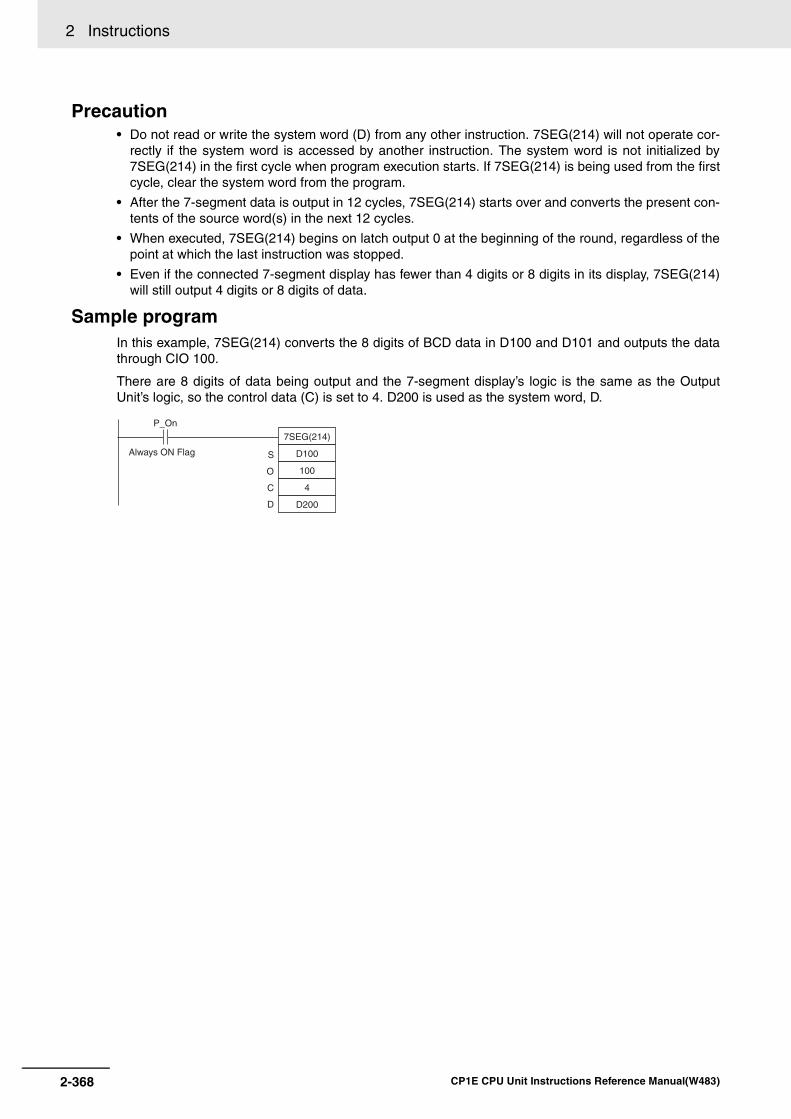
2 Instructions
Precaution• Do not read or write the system word (D) from any other instruction. 7SEG(214) will not operate cor-
rectly if the system word is accessed by another instruction. The system word is not initialized by7SEG(214) in the first cycle when program execution starts. If 7SEG(214) is being used from the firstcycle, clear the system word from the program.
• After the 7-segment data is output in 12 cycles, 7SEG(214) starts over and converts the present con-tents of the source word(s) in the next 12 cycles.
• When executed, 7SEG(214) begins on latch output 0 at the beginning of the round, regardless of thepoint at which the last instruction was stopped.
• Even if the connected 7-segment display has fewer than 4 digits or 8 digits in its display, 7SEG(214)will still output 4 digits or 8 digits of data.
Sample programIn this example, 7SEG(214) converts the 8 digits of BCD data in D100 and D101 and outputs the datathrough CIO 100.
There are 8 digits of data being output and the 7-segment display’s logic is the same as the OutputUnit’s logic, so the control data (C) is set to 4. D200 is used as the system word, D.
S
O
C
D
7SEG(214)
D100
100
4
D200
P_On
Always ON Flag
2-368 CP1E CPU Unit Instructions Reference Manual(W483)

2 Instructions S
erial Co
mm
un
ication
Instru
ction
s
2
TX
D
Serial Communication Instructions
TXD
Applicable Program Areas
Operands
C: Control word
Operand Specifications
Instruction Mnemonic VariationsFunction
codeFunction
TRANSMIT TXD @TXD 236Outputs the specified number of bytes of data from the CPU Unit’s built-in RS-232C port or the Serial Option Board port.
Symbol
TXD
Area Step program areas Subroutines Interrupt tasks
Usage OK OK OK
Operand Description Data type Size
S First source word UINT Variable
C Control word UINT 1
N Number of bytes 0000 to 0100 hex (0 to 256) UINT 1
Area Word addresses Indirect DM addresses
Constants CF Pulse bits TR bitsCIO WR HR AR T C DM @DM *DM
SOK OK OK OK OK OK OK OK OK
------ --- ---
C, N OK
S: First source word
TXD(236)
S
C
N N: Number of bytes0000 to 0100 hex (0 to 256)
C: Control word
15 8 011 37 412
C
Always 0
Byte order0: Most significant bytes first1: Least significant bytes first
RS and ER signal control0: No RS and ER signal control 1: RS signal control2: ER signal control3: RS and ER signal control
Serial port specifier1: CPU Unit’s RS-232C port2: Serial Option Board port / CPU Unit’s RS-485 port
2-369CP1E CPU Unit Instructions Reference Manual(W483)

2 Instructions
Flags
Related Auxiliary Area Words and Bits
CPU Unit’s Built-in RS-232C Port
Serial Option Board Port
Related PLC Setup Settings
Function• TXD(236) reads N bytes of data from words S to S+(N÷2)-1 and outputs the raw data in no-protocol
mode from the CPU Unit’s built-in RS-232C port or the Serial Option Board port. (The output port isspecified with bits 8 to 11 of C.)
• The following send-message frame format can be set in the PLC Setup.
1) Start code: None or 00 to FF hex.
2) End code: None, CR+LF, or 00 to FF hex.
The data will be sent with any start and/or end codes specified in the PLC Setup. If start and endcodes are specified, the codes will be added to the send data (N). In this case, the maximum numberof bytes that can be specified for N is 256 bytes.
• Data is sent in the order specified in C0 to C3.
Name Label Operation
Error Flag P_ER • ON if no-protocol mode is not set in the PLC Setup.
• ON if the value of C is not within range.
• ON if the value for N is not between 0000 and 0100 hex.
• ON if a send is attempted when the Send Ready Flag is OFF. (The Send Ready Flag is A392.05 for the CPU Unit’s RS-232C port, or A392.13 for Serial Option Board port.)
• OFF in all other cases.
Port Address Contents
CPU Unit’s built-in RS-232C port A392.05 ON when data can be sent in the no-protocol mode.
Port Address Contents
Serial Option Board port A392.13 ON when data can be sent in the no-protocol mode.
2-370 CP1E CPU Unit Instructions Reference Manual(W483)

2 Instructions S
erial Co
mm
un
ication
Instru
ction
s
2
TX
D
• Specification of control in C4 to C7 for the RS and ER signals take effect as follows:
1) If RS signal control is specified in C, bit 15 of S will be used as the RS signal.2) If ER signal control is specified in C, bit 15 of S will be used as the ER signal.3) If RS and ER signal control is specified in C, bit 15 of S will be used as the RS signal and bit 14 of S
will be used as the ER signal.
Note 1 For CP1E-NS(1), ER signal is not supported by the built-in RS-232C port, therefore ER signal controlcannot be specified. Bit 4 to 7 of C should not be set to 2 or 3 hex.
2 For CP1E-NS1, RS and ER signals are not supported by the built-in RS-485 port, therefore RS andER signal control cannot be specified. Bit 4 to 7 of C should not be set to 1, 2 or 3 hex.
• If 1, 2, or 3 hex is specified for RS and ER signal control in C, TXD(236) will be executed regardlessof the status of the Send Ready Flag (A392.05, or A392.13 depending on the port being used).
• Up to 259 bytes can be sent, including the send data (N = 256 bytes max.), the start code, and theend code.
• Specify the size of the send data, not including the start code and end code, in N.
Start code / end code settings and send data
Hint• When sending data to another device by TXD instruction, the device may require that the data be
sent at certain intervals. In that case, a transmission delay time can be set to adjust the transmissionintervals.
Precautions• TXD(236) can be used only for the CPU Unit’s RS-232C port or the Serial Option Board port. In addi-
tion, the port must be set to no-protocol mode.
• Data can be sent only when the port’s Send Ready Flag is ON. (The Send Ready Flag is A392.05 forthe CPU Unit’s RS-232C port, or A392.13 for Serial Option Board port.)
• Nothing will be sent if 0 is specified for N.
ED
. . .
. . .ST
. . . ED
. . .ST
LF . . . CR
. . .ST CR LF
CR+LF End Code
Only End Code
No Start or End Code
N send bytes: 256 max.
Only Start Code
Send bytes after ST: 256 max.
Send bytes before ED: 256 max.
Start and End Code
Send bytes between ST and ED: 256 max.
Send bytes before CR+LF: 256 max.
Send bytes between ST and CR+LF: 256 max.
Start and CR+LF End Code
Data sent.
S
S+1
S+2
15 7 08N bytes of data is sent in the following order when sending the most significant bytes first is specified:, , , , ,
CPU Unit’s built-in RS-232C port or Serial Option Board port
2-371CP1E CPU Unit Instructions Reference Manual(W483)
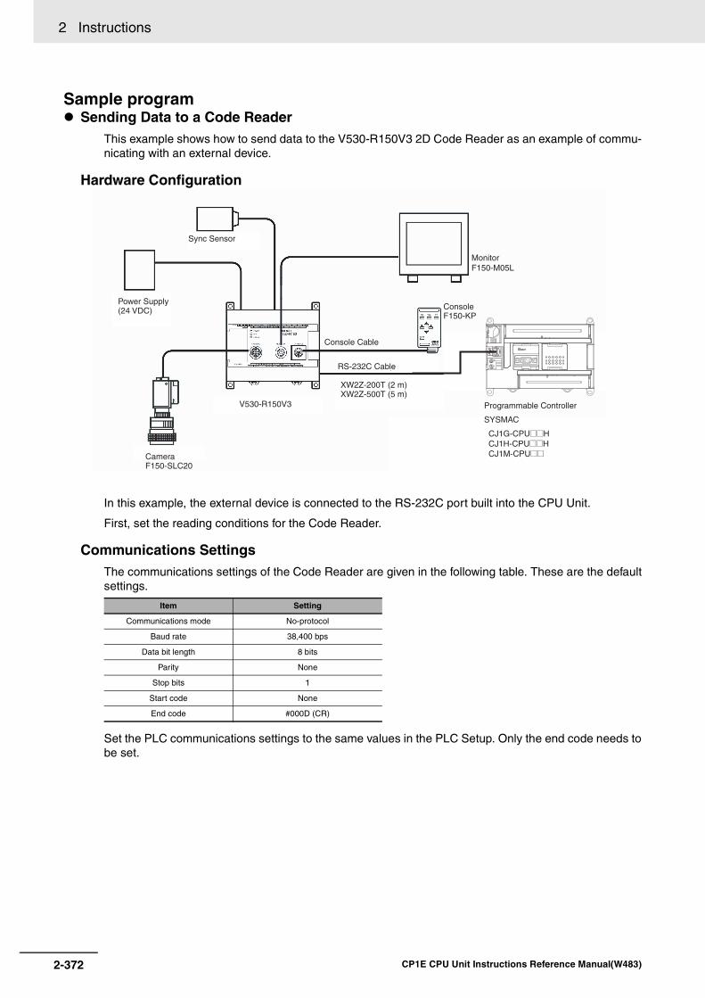
2 Instructions
Sample program Sending Data to a Code Reader
This example shows how to send data to the V530-R150V3 2D Code Reader as an example of commu-nicating with an external device.
Hardware Configuration
In this example, the external device is connected to the RS-232C port built into the CPU Unit.
First, set the reading conditions for the Code Reader.
Communications SettingsThe communications settings of the Code Reader are given in the following table. These are the defaultsettings.
Set the PLC communications settings to the same values in the PLC Setup. Only the end code needs tobe set.
Item Setting
Communications mode No-protocol
Baud rate 38,400 bps
Data bit length 8 bits
Parity None
Stop bits 1
Start code None
End code #000D (CR)
MonitorF150-M05L
ConsoleF150-KP
Console Cable
Programmable Controller
SYSMAC
CJ1G-CPU@@HCJ1H-CPU@@HCJ1M-CPU@@
XW2Z-200T (2 m)XW2Z-500T (5 m)
V530-R150V3
CameraF150-SLC20
RS-232C Cable
Power Supply(24 VDC)
Sync Sensor
2-372 CP1E CPU Unit Instructions Reference Manual(W483)

2 Instructions S
erial Co
mm
un
ication
Instru
ction
s
2
TX
D
Programming ExampleIf CIO 0.01 turns ON while the RS-232C Port Send Ready Flag (A392.05) is ON, three bytes of datastarting from the upper byte of D10 are sent without conversion to the Code Reader connected to theCPU Unit’s built-in RS-232C port. These three bytes contain “@GO”, which is the normal read com-mand used as a trigger input to the Code Reader from the RS-232C line.
Controlling Signals
4 C 00
4 0 74
15 8 71112 34 0
S: D10
@TXD
D10
D20
0.01 A392.05
S
C
&3N
RS-232C Port SendReady Flag
D11
@RXD
D100
D20
0.02 A392.06
A393
RS-232C Port ReceiveReady Flag
RS-232C PortReception Counter
Always #0.
Serial Port Specifier
#1: CPU Unit’s built-in RS-232C port
0 1 00
15 8 71112 34 0
C: D20
RS and ER Signal Control
#0: No RS and ER signal control.
Byte Order
#0: Most significant bytes first
Three bytes
Lower byteUpper byte
40 47 4C ED
Sent @ G L
TXD
D300
D400
0.01
S
C
&0N
0 1 03
15 8 71112 34 0
C: D400
0
15 1314 12
S: D300
Turns OFF ER signal.
001
Turns ON RS signal.
Always #0.
Serial Port Specifier#1: CPU Unit’s built-in RS-232C port
RS and ER Signal Control #3: RS and ER signal control
Byte Order#0: Most significant bytes first
When CIO 0.01 turns ON, the status of bit 15 of D300 is output as the RS signal and the status of bit 14 is output as the ER signal.
2-373CP1E CPU Unit Instructions Reference Manual(W483)

2 Instructions
RXD
Applicable Program Areas
Operands
C: Control Word
Operand Specifications
Flags
Instruction Mnemonic VariationsFunction
codeFunction
RECEIVE RXD @RXD 235Reads the specified number of bytes of data from the CPU Unit’s built-in RS-232C port or the Serial Option Board port.
Symbol
RXD
Area Step program areas Subroutines Interrupt tasks
Usage OK OK OK
Operand Description Data type Size
D First destination word UINT Variable
C Control word UINT 1
N Number of bytes to store 0000 to 0100 hex (0 to 256 decimal) UINT 1
Area Word addresses Indirect DM addresses
Constants CF Pulse bits TR bitsCIO WR HR AR T C DM @DM *DM
DOK OK OK OK OK OK OK OK OK
------ --- ---
C, N OK
Name Label Operation
Error Flag P_ER • ON if no-protocol mode is not set in the PLC Setup.
• ON if the value of C is not within range.
• ON if the value for N is not between 0000 and 0100 hex.
• OFF in all other cases.
RXD(235)
D
C
N
D: First destination word
C: Control word
N: Number of bytes to store 0000 to 0100 hex (0 to 256 decimal)
C
812 3415 0711
Byte order0 Hex: Most significant byte to least significant byte1 Hex: Lest significant byte to most significant byte
CS and DR signal monitoring 0: No CS and DR signal monitoring 1: CS signal monitoring2: DR signal monitoring3: CS and DR signal monitoring.
Always 0
Serial port specifier1: CPU Unit’s RS-232C port2: Serial Option Board port / CPU Unit’s RS-485 port
2-374 CP1E CPU Unit Instructions Reference Manual(W483)
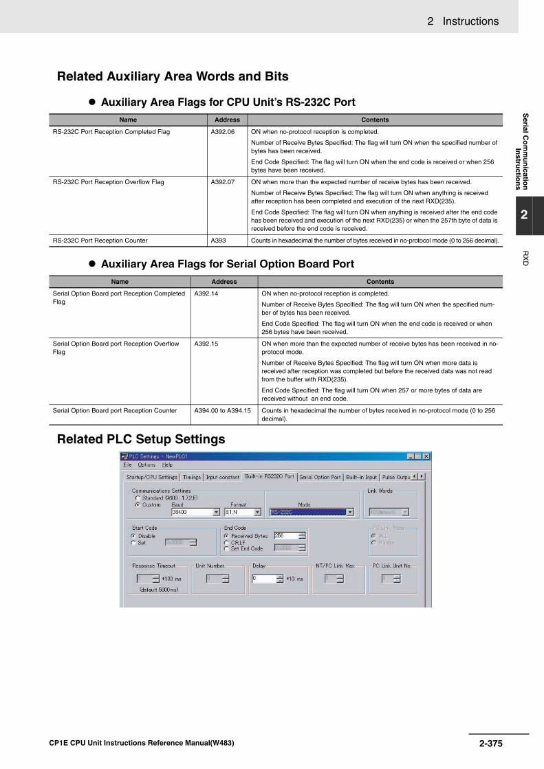
2 Instructions S
erial Co
mm
un
ication
Instru
ction
s
2
RX
D
Related Auxiliary Area Words and Bits
Auxiliary Area Flags for CPU Unit’s RS-232C Port
Auxiliary Area Flags for Serial Option Board Port
Related PLC Setup Settings
Name Address Contents
RS-232C Port Reception Completed Flag A392.06 ON when no-protocol reception is completed.
Number of Receive Bytes Specified: The flag will turn ON when the specified number of bytes has been received.
End Code Specified: The flag will turn ON when the end code is received or when 256 bytes have been received.
RS-232C Port Reception Overflow Flag A392.07 ON when more than the expected number of receive bytes has been received.
Number of Receive Bytes Specified: The flag will turn ON when anything is received after reception has been completed and execution of the next RXD(235).
End Code Specified: The flag will turn ON when anything is received after the end code has been received and execution of the next RXD(235) or when the 257th byte of data is received before the end code is received.
RS-232C Port Reception Counter A393 Counts in hexadecimal the number of bytes received in no-protocol mode (0 to 256 decimal).
Name Address Contents
Serial Option Board port Reception Completed Flag
A392.14 ON when no-protocol reception is completed.
Number of Receive Bytes Specified: The flag will turn ON when the specified num-ber of bytes has been received.
End Code Specified: The flag will turn ON when the end code is received or when 256 bytes have been received.
Serial Option Board port Reception Overflow Flag
A392.15 ON when more than the expected number of receive bytes has been received in no-protocol mode.
Number of Receive Bytes Specified: The flag will turn ON when more data is received after reception was completed but before the received data was not read from the buffer with RXD(235).
End Code Specified: The flag will turn ON when 257 or more bytes of data are received without an end code.
Serial Option Board port Reception Counter A394.00 to A394.15 Counts in hexadecimal the number of bytes received in no-protocol mode (0 to 256 decimal).
2-375CP1E CPU Unit Instructions Reference Manual(W483)

2 Instructions
Function• RXD(235) reads data that has been received in no-protocol mode at the CPU Unit’s built-in RS-232C
port or the Serial Option Board port (the port is specified with bits 8 to 11 of C) and stores N bytes ofdata in words D to D+(N÷2)-1. If N bytes of data has not been received at the port, then only the datathat has been received will be stored.
• The following receive message frame format can be set in the PLC Setup.
1) Start code: None or 00 to FF hex
2) End code: None, CR+LF, or 00 to FF hex. If no end code is specified, the number of bytes toreceived is set from 00 to FF hex (1 to 256 decimal; 00 specifies 256 bytes).
• Data will be stored in memory in the order specified in C0 to C3.• Cases where the reception completion flag turns ON
The Reception Completed Flag (note (a)) will turn ON when the number of bytes specified in the PLCSetup has been received. When the Reception Completed Flag turns ON, the number of bytes in theReception Counter (note (b)) will have the same value as the number of receive bytes specified in thePLC Setup.If an end code is specified in the PLC Setup, the Reception Completed Flag (note (a)) will turn ONwhen the end code is received or when 256 bytes of data have been received. If more bytes arereceived than specified, the Reception Overflow Flag (note (c)) will turn ON.
• When RXD(235) is executed, data is stored in memory starting at D, the Reception Completed Flag(note (a)) will turn OFF (even if the Reception Overflow Flag (note (c)) is ON), and the ReceptionCounter (note (b)) will be cleared to 0.
• If the RS-232C Port Restart Bit (note (d)) is turned ON, the Reception Completed Flag (note (a)) willbe turned OFF (even if the Reception Overflow Flag is ON), and the Reception Counter (note (b)) willbe cleared to 0.
• Specification of monitor in bits C4 to C7 for the CS and DR signals takes effect as follows:
1) If CS signal monitoring is specified in C, the status of the CS signal will be stored in bit 15 of D.
2) If DR signal monitoring is specified in C, the status of the DR signal will be stored in bit 15 of D.
3) If CS and DR signal monitoring is specified in C, the status of the CS signal will be stored in bit 15of D and the status of the DR signal will be stored in bit 14 of D.
Note 1 For CP1E-NS(1), DR signal is not supported by the built-in RS-232C port, therefore DR signal moni-toring cannot be specified. Bit 4 to 7 of C should not be set to 2 or 3 hex.
2 For CP1E-NS1, CS and DR signals are not supported by the built-in RS-485 port, therefore CS andDR signal monitoring cannot be specified. Bit 4 to 7 of C should not be set to 1, 2 or 3 hex.
• If 1, 2, or 3 hex is specified for CS and DR signal control in C, RXD(235) will be executed regardlessof the status of the Receive Completed Flag (note (a)).
• Receive data will not be stored if CS or DR signal monitoring is specified.• Up to 259 bytes can be received, including the receive data (N = 256 bytes max.), the start code, and
the end code.• Specify the size of the receive data, not including the start code and end code, in N.
Note Related Auxiliary Area and CIO Area Addresses(a) Reception Completed Flags
Built-in RS232C port A392.06
Serial Option Board port: A392.14
(b) Reception Counters
Built-in RS232C port A393
Serial Option Board port: A394
(c) Reception Overflow Flags
Built-in RS232C port A392.07
Serial Option Board port: A392.15
(d) RS-232C Port Restart Bit
Built-in RS232C port A526.00
Serial Option Board port: A526.01
2-376 CP1E CPU Unit Instructions Reference Manual(W483)

2 Instructions S
erial Co
mm
un
ication
Instru
ction
s
2
RX
D
Start Code/End Code Settings and Receive Data
Hint• When RXD(235) is used to read data that was received at one of the Serial Option Board’s ports , the
port’s reception buffer is cleared after RXD(235) is executed. Consequently, RXD(235) can not beexecuted repeatedly to read a block of data in parts.
Precautions• RXD(235) can be used only for the CPU Unit’s RS-232C port or the Serial Option Board port. In addi-
tion, the port must be set to no-protocol mode.
• Execute this instruction when the reception completion flag (RS-232C incorporated in the CPU unit:A392.06, Serial Option Board: A392.14) is 1 (ON) to receive data (from the reception buffer).
• When data is received, the data must be read by an RXD instruction or the next data cannot bereceived. When the reception completion flag turns ON, read the received data with an RXD instruc-tion before the next reception.
• Specify the size of the receive data, not including the start code and end code, in N.
• If 0 is specified for N, the Reception Completed Flag and Reception Overflow Flag (note(a)) will beturned OFF, the Reception Counter (note(b)) will be cleared to 0, and nothing will be stored in memory.
1 2 3 4 5 6 0...
1 2 3 4 5 6 0...
1 2 3 4 5 6 0...
1 2 3 4 5 6 0...
1 2 3 4 5 6 0...
1 2 3 4 5 6 0...
1
3
5
2
4
6
1
3
5
2
4
6
1
2
3
4
5
6
LFCR
Bytes
Receive bytes: Specified in the PC Setup
Receive bytes after ST: Specified in the PC Setup
Receive bytes before ED: 256 max.
Receive bytes between ST and ED: 256 max.
Receive bytes before CR+LF: 256 max.
Receive bytes between ST and CR+LF: 256 max.
When receiving the most significant bytes first is specified (0):
Most signifi-cant bytes
Least signif-icant bytes
When receiving the least significant bytes first is specified (1):
Most signifi-cant bytes
Least signif-icant bytes
N bytes stored in the specified
Max: 256 bytes order.
Received
CPU Unit’s built-in RS-232C portor Serial Option Board port
Start and CR+LF End Code
CR+LF End Code
Start and End Code
Only End Code
Only Start Code
No Start or End Code
ED
ST
ED
ST
ST CR LF
D
D+1
D+2
15 7 08
D
D+1
D+2
15 7 08
2-377CP1E CPU Unit Instructions Reference Manual(W483)

2 Instructions
Sample program Receiving data
This example shows how to receive data from the V530-R150V3 2D Code Reader as an example ofcommunicating with an external device.
Hardware Configuration
In this example, the external device is connected to the RS-232C port built into the CPU Unit.
First, set the reading conditions for the Code Reader.
Communications SettingsThe communications settings of the Code Reader are given in the following table. These are the defaultsettings.
Set the PLC communications settings to the same values in the PLC Setup. Only the end code needs tobe set.
Item Setting
Communications mode No-protocol
Baud rate 38,400 bps
Data bit length 8 bits
Parity None
Stop bits 1
Start code None
End code #000D (CR)
MonitorF150-M05L
ConsoleF150-KP
Console Cable
Programmable Controller
SYSMAC
CJ1G-CPU HCJ1H-CPU HCJ1M-CPU
XW2Z-200T (2 m)XW2Z-500T (5 m)
V530-R150V3
CameraF150-SLC20
RS-232C Cable
Power Supply(24 VDC)
Sync Sensor
2-378 CP1E CPU Unit Instructions Reference Manual(W483)

2 Instructions S
erial Co
mm
un
ication
Instru
ction
s
2
RX
D
Programming ExampleIf CIO 0.02 turns ON while the RS-232C Port Send Ready Flag (A392.05) is ON, the number of bytes ofreading results specified in the RS-232C Port Reception Counter (A393) are read from the CodeReader connected to the CPU Unit’s built-in RS-232C port and stored starting from the upper byte ofD100.
Controlling Signals
2 F 03
3 0 63
15 8 71112 34 0
S: D100
TXD
D10
D20
0.01 A392.05
S
C
&3
N
D101
RXD
D100
D20
0.02 A392.06
A393
0 1 00
15 8 71112 34 0
C: D20
D102 3 8 F2
D103 3 1 13
=”06/08/11
Received
30 36 2F 30 38 2F 31 31
RS-232C Port SendReady Flag
RS-232C Port ReceiveReady Flag
RS-232C PortReception Counter
Always #0.
Serial Port Specifier
#1: CPU Unit’s built-in RS-232C port
RS and ER Signal Control
#0: No RS and ER signal control
Byte Order
#0: Most significant bytes first
Lower byteUpper byte
RXD
D100
D200
0.00
D
C
&10N
0 1 03
15 8 71112 34 0
C: D200
0
15 1314 12
D: D100 001
DR signal: 0
CS signal: 1
Always #0.
Serial Port Specifier#1: CPU Unit’s built-in RS-232C port
CS and DR Signal Monitor #3: CS and DR signal monitor
Byte Order#0: Most significant bytes first
When CIO 0.00 turns ON, the status of the CS signal is output to bit 15 of D100 and the status of the DR signal is output to bit 14 of D100.
2-379CP1E CPU Unit Instructions Reference Manual(W483)

2 Instructions
Clock Instructions
CADD/CSUB
Applicable Program Areas
Operands
Instruction Mnemonic VariationsFunction
codeFunction
CALENDAR ADD CADD @CADD 730Adds time to the calendar data in the specified words.
CALENDAR SUBTRACT CSUB @CSUB 731Subtracts time from the calendar data in the spec-ified words.
Symbol
CADD CSUB
Area Step program areas Subroutines Interrupt tasks
Usage OK OK OK
Operand Description Data type Size
C First calendar word WORD 3
T First time word DWORD 2
R First result word WORD 3
C: First calendar word
T: First time word
R: First result word
CADD(730)
C
T
R
C: First calendar word
T: First time word
R: First result word
CSUB(731)
C
T
R
2-380 CP1E CPU Unit Instructions Reference Manual(W483)

2 Instructions C
lock In
structio
ns
2
CA
DD
/CS
UB
CADDC through C+2: Calendar Data T and T+1: Time Data
R through R+2: Result Data
15 8 07
C
15 8 07
C+1
15 8 07
C+2
Seconds: 00 to 59 (BCD)
Minutes: 00 to 59 (BCD)
Hour: 00 to 23 (BCD)
Month: 01 to 12 (BCD)
Year: 00 to 99 (BCD)
Day: 01 to 31 (BCD)
15 8 07
T
15 0
T+1
Seconds: 00 to 59 (BCD)
Minutes: 00 to 59 (BCD)
Hours: 0000 to 9999 (BCD)
15 8 07
R
15 8 07
R+1
15 8 07
R+2
Seconds: 00 to 59 (BCD)
Minutes: 00 to 59 (BCD)
Hour: 00 to 23 (BCD)
Day: 01 to 31 (BCD)
Month: 01 to 12 (BCD)
Year: 00 to 99 (BCD)
2-381CP1E CPU Unit Instructions Reference Manual(W483)

2 Instructions
CSUBC through C+2: Calendar Data T and T+1: Time Data
R through R+2: Result Data
15 8 07
C
15 8 07C+1
15 8 07
C+2
Minutes: 00 to 59 (BCD)
Seconds: 00 to 59 (BCD)
Day: 01 to 31 (BCD)
Hour: 00 to 23 (BCD)
Year: 00 to 99 (BCD)
Month: 01 to 12 (BCD)
15 8 07
T
15 0
T+1
Seconds: 00 to 59 (BCD)
Minutes: 00 to 59 (BCD)
Hours: 0000 to 9999 (BCD)
15 8 07
R
15 8 07
R+1
15 8 07
R+2
Seconds: 00 to 59 (BCD)
Minutes: 00 to 59 (BCD)
Hour: 00 to 23 (BCD)
Day: 01 to 31 (BCD)
Month: 01 to 12 (BCD)
Year: 00 to 99 (BCD)
2-382 CP1E CPU Unit Instructions Reference Manual(W483)
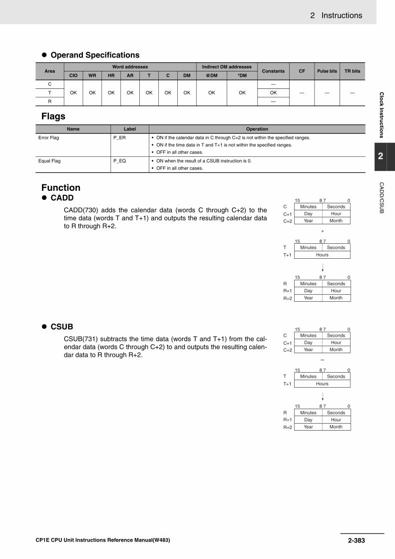
2 Instructions C
lock In
structio
ns
2
CA
DD
/CS
UB
Operand Specifications
Flags
Function CADD
CADD(730) adds the calendar data (words C through C+2) to thetime data (words T and T+1) and outputs the resulting calendar datato R through R+2.
CSUBCSUB(731) subtracts the time data (words T and T+1) from the cal-endar data (words C through C+2) to and outputs the resulting calen-dar data to R through R+2.
Area Word addresses Indirect DM addresses
Constants CF Pulse bits TR bitsCIO WR HR AR T C DM @DM *DM
C
OK OK OK OK OK OK OK OK OK
---
--- --- ---T OK
R ---
Name Label Operation
Error Flag P_ER • ON if the calendar data in C through C+2 is not within the specified ranges.
• ON if the time data in T and T+1 is not within the specified ranges.
• OFF in all other cases.
Equal Flag P_EQ • ON when the result of a CSUB instruction is 0.
• OFF in all other cases.
C+1
C
C+2
T+1
T
R+1
R
R+2
+
15 7 08
15 7 08
15 7 08Minutes Seconds
Day Hour
Year Month
Minutes Seconds
Minutes Seconds
Day Hour
Year Month
Hours
C+1
C
C+2
T+1
T
R+1
R
R+2
-
15 7 08
15 7 08
15 7 08Minutes Seconds
Day Hour
Year Month
Minutes Seconds
Minutes Seconds
Day Hour
Year Month
Hours
2-383CP1E CPU Unit Instructions Reference Manual(W483)
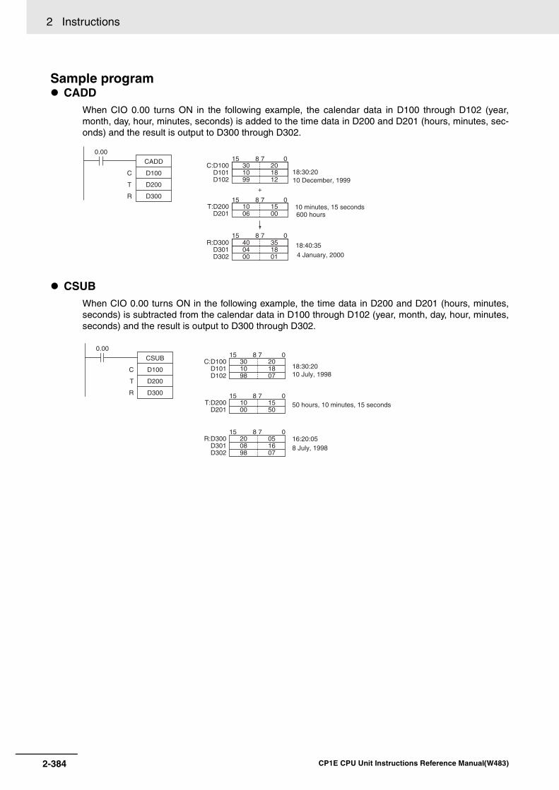
2 Instructions
Sample program CADD
When CIO 0.00 turns ON in the following example, the calendar data in D100 through D102 (year,month, day, hour, minutes, seconds) is added to the time data in D200 and D201 (hours, minutes, sec-onds) and the result is output to D300 through D302.
CSUBWhen CIO 0.00 turns ON in the following example, the time data in D200 and D201 (hours, minutes,seconds) is subtracted from the calendar data in D100 through D102 (year, month, day, hour, minutes,seconds) and the result is output to D300 through D302.
CADD
D100
D200
D300
0.00
C
T
R
C:D100D101D102
301099
201812
15 7 08
08
08
T:D200D201
1006
+
1500
15 7
R:D300D301D302
4004 00
3518 01
15 7
18:30:20
18:40:35
10 December, 1999
10 minutes, 15 seconds600 hours
4 January, 2000
CSUB
D100
D200
D300
0.00
C
T
R
C:D100D101D102
301098
201807
15 78 0
T:D200D201
1000
1550
15 78 0
R:D300D301D302
200898
051607
15 78 0
18:30:20
16:20:05
10 July, 1998
50 hours, 10 minutes, 15 seconds
8 July, 1998
2-384 CP1E CPU Unit Instructions Reference Manual(W483)
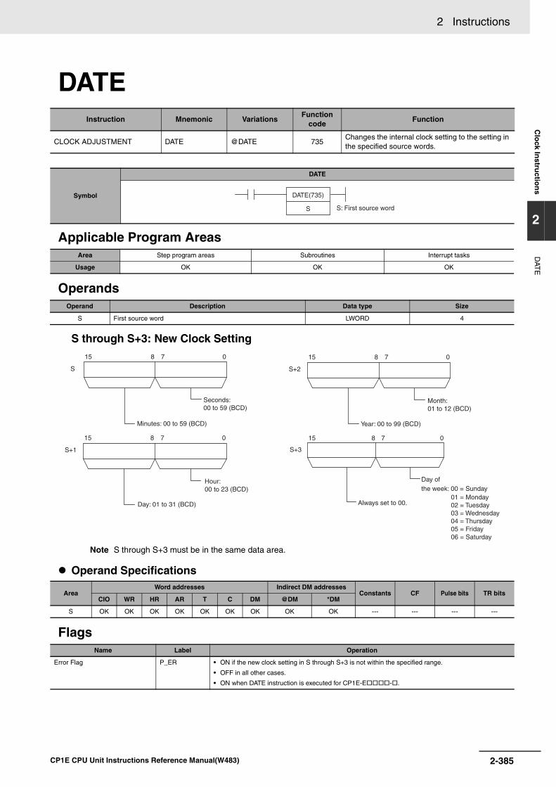
2 Instructions C
lock In
structio
ns
2
DAT
E
DATE
Applicable Program Areas
Operands
S through S+3: New Clock Setting
Note S through S+3 must be in the same data area.
Operand Specifications
Flags
Instruction Mnemonic VariationsFunction
codeFunction
CLOCK ADJUSTMENT DATE @DATE 735Changes the internal clock setting to the setting in the specified source words.
Symbol
DATE
Area Step program areas Subroutines Interrupt tasks
Usage OK OK OK
Operand Description Data type Size
S First source word LWORD 4
Area Word addresses Indirect DM addresses
Constants CF Pulse bits TR bitsCIO WR HR AR T C DM @DM *DM
S OK OK OK OK OK OK OK OK OK --- --- --- ---
Name Label Operation
Error Flag P_ER • ON if the new clock setting in S through S+3 is not within the specified range.
• OFF in all other cases.
• ON when DATE instruction is executed for CP1E-E-.
S: First source word
DATE(735)
S
15 8 07
S
15 8 07
S+1
15 8 07
S+2
15 8 07
S+3
Seconds: 00 to 59 (BCD)
Minutes: 00 to 59 (BCD)
Hour: 00 to 23 (BCD)
Day: 01 to 31 (BCD)
Month: 01 to 12 (BCD)
Year: 00 to 99 (BCD)
Always set to 00.
Day of the week: 00 = Sunday
01 = Monday02 = Tuesday03 = Wednesday 04 = Thursday05 = Friday06 = Saturday
2-385CP1E CPU Unit Instructions Reference Manual(W483)

2 Instructions
Related Auxiliary Area Words and Bits
FunctionDATE(735) changes the internal clocksetting according to the clock data inthe four source words. The new inter-nal clock setting is immediatelyreflected in the Calendar/Clock Area(A351 to A354).
HintThe internal clock setting can also be changed from a Peripheral Device or the CLOCK WRITE FINScommand (0702).
Precaution• An error will not be generated even if the internal clock is set to a non-existent date (such as Novem-
ber 31).
• In case this instruction is executed for E-type CPU Unit (CP1E-E-), the error flag will turnON and the instruction cannot be executed. For E-type CPU Unit, A351 to A354 is always 01-01-0101:01:01 Sunday.
Sample programWhen CIO 0.00 turns ON in the following example, the internal clock is set to 20:15:30 on Thursday,October 9, 1998.
Name Address Operation
Clock data A351 to A354 A351.00 to A351.07: Seconds (00 to 59) (BCD)
A351.08 to A351.15: Minutes (00 to 59) (BCD)
A352.00 to A352.07: Hours (00 to 23) (BCD)
A352.08 to A352.15: Day of the month (01 to 31) (BCD)
A353.00 to A353.07: Month (01 to 12) (BCD)
A353.08 to A353.15: Year (00 to 99) (BCD)
A354.00 to A354.07: Day of the week (00 to 06) (BCD)
00: Sunday, 01: Monday, 02: Tuesday, 03: Wednesday, 04: Thursday,
05: Friday, 06: Saturday
S1
S+1
S+2
S+3
Internal clock
New setting
00
Minutes
Day
Year
Day of week
Seconds
Hour
Month
CPU Unit
DATE
D100
0.00
SS:D100 15 30
15 78
D101 09 2015 78
D102 98 1015 78
D103 00 0415 78
0
0
0
0
Second
Hour
Minute
Day ofthe month
Year Month
Always set to 00.
Day of the week
2-386 CP1E CPU Unit Instructions Reference Manual(W483)

2 Instructions Failu
re Diag
no
sis Instru
ction
s
2
FAL
Failure Diagnosis Instructions
FAL
Applicable Program Areas
Operands
Generating or Clearing User-defined Non-fatal Errors
Note The value of operand N must be different from the content of A529 (the system-generated FAL/FALS number).
Generating Non-fatal System Errors
Note The value of operand N must be the same as the content of A529 (the system-generated FAL/FALS number).
Operand Specifications
Instruction Mnemonic VariationsFunction
codeFunction
FAILURE ALARM FAL @FAL 006Generates or clears user-defined non-fatal errors. Non-fatal errors do not stop PLC operation.
Symbol
FAL
Generating or Clearing User-defined Non-fatal Errors Generating Non-fatal System Errors
Area Step program areas Subroutines Interrupt tasks
Usage OK OK OK
Operand Description Data type Size
N FAL number Constants only 1
SFirst message word or constant / First word containing the error code and error details
WORD Variable
Generates a non-fatal error Clears all non-fatal errors
N 1 to 511 (These FAL numbers are shared with FALS numbers.) 0
S
Word address:Generates a non-fatal error with the corresponding FAL number.The 16-character ASCII message contained in S through S+7 will be displayed on the Programming Device.#0000 to #FFFF:Generates a non-fatal error with the corresponding FAL number (no message).
#FFFF: Clears all non-fatal errors.
#0001 to #01FF: Clears the non-fatal error with the corresponding FAL number.
Other: Clears the most serious non-fatal error.
Generates a non-fatal error
N 1 to 511 (These FAL numbers are shared with FALS numbers.)
S Error code that will be generated. (See Function below.)
S+1 Error details code that will be generated. (See Function below.)
Area Word addresses Indirect DM addresses
Constants CF Pulse bits TR bitsCIO WR HR AR T C DM @DM *DM
N --- --- --- --- --- --- --- --- ---OK --- --- ---
S OK OK OK OK OK OK OK OK OK
N: FAL number
S: First message word or constant (0000 to FFFF)
FAL(006)
N
S
N: FAL number (value in A529)
S: First word containing the error code and error details
FAL(006)
N
S
2-387CP1E CPU Unit Instructions Reference Manual(W483)
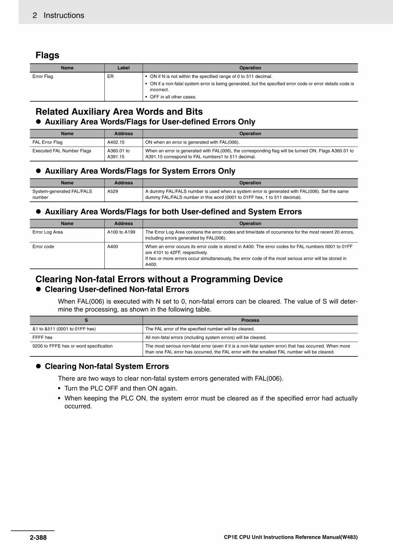
2 Instructions
Flags
Related Auxiliary Area Words and Bits Auxiliary Area Words/Flags for User-defined Errors Only
Auxiliary Area Words/Flags for System Errors Only
Auxiliary Area Words/Flags for both User-defined and System Errors
Clearing Non-fatal Errors without a Programming Device Clearing User-defined Non-fatal Errors
When FAL(006) is executed with N set to 0, non-fatal errors can be cleared. The value of S will deter-mine the processing, as shown in the following table.
Clearing Non-fatal System ErrorsThere are two ways to clear non-fatal system errors generated with FAL(006).
• Turn the PLC OFF and then ON again.
• When keeping the PLC ON, the system error must be cleared as if the specified error had actuallyoccurred.
Name Label Operation
Error Flag ER • ON if N is not within the specified range of 0 to 511 decimal.
• ON if a non-fatal system error is being generated, but the specified error code or error details code is incorrect.
• OFF in all other cases.
Name Address Operation
FAL Error Flag A402.15 ON when an error is generated with FAL(006).
Executed FAL Number Flags A360.01 to A391.15
When an error is generated with FAL(006), the corresponding flag will be turned ON. Flags A360.01 to A391.15 correspond to FAL numbers1 to 511 decimal.
Name Address Operation
System-generated FAL/FALS number
A529 A dummy FAL/FALS number is used when a system error is generated with FAL(006). Set the same dummy FAL/FALS number in this word (0001 to 01FF hex, 1 to 511 decimal).
Name Address Operation
Error Log Area A100 to A199 The Error Log Area contains the error codes and time/date of occurrence for the most recent 20 errors, including errors generated by FAL(006).
Error code A400 When an error occurs its error code is stored in A400. The error codes for FAL numbers 0001 to 01FF are 4101 to 42FF, respectively.If two or more errors occur simultaneously, the error code of the most serious error will be stored in A400.
S Process
&1 to &511 (0001 to 01FF hex) The FAL error of the specified number will be cleared.
FFFF hex All non-fatal errors (including system errors) will be cleared.
0200 to FFFE hex or word specification The most serious non-fatal error (even if it is a non-fatal system error) that has occurred. When more than one FAL error has occurred, the FAL error with the smallest FAL number will be cleared.
2-388 CP1E CPU Unit Instructions Reference Manual(W483)
2 Instructions Failu
re Diag
no
sis Instru
ction
s
2
FAL
Function Generating Non-fatal User-defined Errors
The following table shows the error codes and FAL Error Flags for FAL(006).
When FAL(006) is executed with N set to an FAL number (&1 to &511) that is not equal to the content ofA529 (the system-generated FAL/FALS number), a non-fatal error will be generated with that FAL num-ber and the following processing will be performed:
1. The FAL Error Flag (A402.15) will be turned ON. (PLC operation will continue.)
2. The Executed FAL Number Flag will be turned ON for the corresponding FAL number. Flags A360.01to A391.15 correspond to FAL numbers 0001 to 01FF (1 to 511).
3. The error code will be written to A400. Error codes 4101 to 42FF correspond to FAL numbers 0001 to01FF (1 to 511).
4. The error code and the time that the error occurred will be written to the Error Log Area (A100through A199).
Note The error record will not be written to the Error Log Area if the Don’t register FAL to error log Option in thePLC Setup is selected.
5. The ERR Indicator on the CPU Unit will flash.
6. If a word address has been specified in S, the message beginning at S will be registered (displayedon the Programming Device).
Note If a fatal error or a more serious non-fatal error occurs at the same time as the FAL(006) instruction, the moreserious error’s error code will be written to A400.
Generating Non-fatal System ErrorsWhen FAL(006) is executed with N set to an FAL number (&1 to &511) that is equal to the content ofA529 (the system-generated FAL/FALS number), a non-fatal error will be generated with the error codeand error details code specified in S and S+1. The following processing will be performed at the sametime:
FAL number 1 to 511 decimal
FAL error codes 4101 to 42FF
Executed FAL Number Flags A360.01 to A391.15
FAL Error Flag ON
Corresponding Executed FAL Number Flag ON
Error code written to A400
Error code and time written to Error Log Area
ERR Indicator flashes
Execution of FAL(006) generates a non-fatal er-ror with FAL number N.
FAL
N
0000
FAL
N
S
NA529CH
S
S+1
Execution of FAL(006) generates a non-fatal system error with the error code/details specified in S and S+1.
Error code written to A400
Error code and time written to Error Log Area
The corresponding Auxiliary Area Flags are set based on the error code and error details.
ERR Indicator flashes.Matching values
Error code
Error details
2-389CP1E CPU Unit Instructions Reference Manual(W483)

2 Instructions
1. The specified error code will be written to A400.
2. The error code and the time that the error occurred will be written to the Error Log Area (A100through A199).
3. The appropriate Auxiliary Area Flags are set based on the error code and error details.
4. The ERR Indicator on the CPU Unit will flash and PLC operation will continue.
Note 1 FAL(006) can be used to generate non-fatal errors from the system when debugging the program. Forexample, a system error can be generated intentionally to check whether or not error messages are beingdisplayed properly at an interface such as a Programmable Terminal (PT).
2 The value of A529 (the system-generated FAL/FALS number) is a dummy FAL number (FAL and FALSnumbers are shared.) used when a non-fatal error is generated intentionally by the system. This number isa dummy FAL number, so it does not change the status of the Executed FAL Number Flags (A360.01 toA391.15) or the error code.When it is necessary to generate two or more system errors (fatal and/or non-fatal errors), different errorscan be generated by executing the FAL/FALS instructions more than once with the same values in A529and N, but different values in S and S+1.
3 If a more serious error (including a system-generated fatal error or FALS(007) error) occurs at the sametime as the FAL(006) instruction, the more serious error’s error code will be written to A400.
4 To clear a system error generated by FAL(006), turn the PLC OFF and then ON again. The PLC can bekept ON, but the same processing will be required to clear the error as if the specified error had actuallyoccurred.Refer to CP1E CPU Unit Hardware Operation Manual or CP1E CPU Unit Software Operation Manual.
The following table shows how to specify error codes and error details in S and S+1.
Disabling Error Log Entries of User-defined ErrorsNormally when FAL(006) generates a user-defined error, the error code and the time that the erroroccurred are written to the Error Log Area (A100 through A199). It is possible to set the PLC Setup sothat user-defined errors generated by FAL(006) are not recorded in the Error Log.
Note Even though the error will not be recorded in the Error Log, the FAL Error Flag (402.15) will be turned ON,the corresponding flag in the Executed FAL Number Flags (A360.01 to A391.15) will be turned ON, and theerror code will be written to A400.
Disable Error Log entries for user-defined FAL(006) errors when you want to record only the system-generated errors. For example, this function is useful during debugging if the FAL(006) instructions areused in several applications and the Error Log is becoming full of user-defined FAL(006) errors.
• The following screen capture shows the PLC Setup setting from the CX-Programmer.
Error name S S+1
PLC Setup Error 009B hex PLC Setup Error Location0000 to FFFF hex
Built-in Analog Error 008A hex --- (not fixed)
Option Board Error 00D1 hex Option Board Slot No.0001 hex
Battery Error 00F7 hex --- (not fixed)
2-390 CP1E CPU Unit Instructions Reference Manual(W483)
2 Instructions Failu
re Diag
no
sis Instru
ction
s
2
FAL
Note Even if PLC Setup word 129 bit 15 is set to 1 (Do not record FAL Errors in Error Log.), the following errors willbe recorded:
• Fatal errors generated by FALS(007)
• Non-fatal errors from the system
• Fatal errors from the system
• Non-fatal errors from the system generated intentionally with FAL(006)
• Fatal errors from the system generated intentionally with FALS(007)
Displaying Messages with Non-fatal User-defined Errors• If S is a word address and an ASCII message has been stored at S, that message will be displayed at
the Peripheral Device when FAL(006) is executed. (If a message is not required, set S to a constant.)
• The message beginning at S will be registered when FAL(006) is executed. Once the message is reg-istered, it will be displayed.
• An ASCII message up to 16 characters long can be stored in S through S+7. The leftmost (most sig-nificant) byte in each word is displayed first.
• The end code for the message is the null character (00 hexadecimal).
• All 16 characters in words S to S+7 will be displayed if the null character is omitted.
• If the contents of the words containing the message are changed after FAL(006) is executed, themessage will change accordingly.
Sample program Generating a Non-fatal Error
When CIO 0.00 is ON in the following example, FAL(006) will generate a non-fatal error with FAL num-ber 31 and execute the following processes.
1. The FAL Error Flag (A402.15) will be turned ON.
2. The corresponding Executed FAL Number Flag (A361.15) will be turned ON.
3. The corresponding error code (411F) will be written to A400.
4. The error code and the time/date that the error occurred will be written to the Error Log Area (A100through A199).
5. The ERR Indicator on the CPU Unit will flash.
6. The ASCII message in D100 to D107 will be displayed at the Peripheral Device.
Note If a message is not required, specify a constant for S.
Note If two or more errors occur at the same time, the error code of the most serious error (with the highest errorcode) will be stored in A400.
M:
MESSAGELOW VOLTAGE
15 0
4C
57
56
4C
41
45
4F
20
4F
54
47
00
M
N
Disregarded
31
FAL
D100
0.00
M: D100
D101
D102
D103
D104
D105
D106
D107
2-391CP1E CPU Unit Instructions Reference Manual(W483)

2 Instructions
Clearing a Particular Non-fatal ErrorWhen CIO 0.01 is ON in the following example, FAL(006) will clear the non-fatal error with FAL number31, turn OFF the corresponding Executed FAL Number Flag (A361.15), and turn OFF the FAL ErrorFlag (A402.15).
Clearing All Non-fatal ErrorsWhen CIO 0.02 is ON in the following example, FAL(006) will clear all of the non-fatal errors, turn OFFthe Executed FAL Number Flags (A360.01 to A391.15), and turn OFF the FAL Error Flag (A402.15).
Clearing the Most Serious Non-fatal ErrorWhen CIO 0.03 is ON in the following example, FAL(006) will clear the most serious non-fatal error thathas occurred and reset the error code in A400. If the cleared error was originally generated byFAL(006), the corresponding Executed FAL Number Flag and the FAL Error Flag (A402.15) will beturned OFF.
Generating a Non-fatal System ErrorWhen CIO 0.00 is ON in the following example, FAL(006) will generate Option Board Error. In this case,dummy FAL number 10 is used and the corresponding value (000A hex) is stored in A529.
1. The specified error code (00D1) will be written to A400 if it is the most serious error.
2. The error code and the time/date that the error occurred will be written to the Error Log Area (A100through A199).
3. Option Board Error Flag(A315.13) will be turned ON.
4. The CPU Unit’s ERR Indicator will flash.
5. Option Board Error will occur.
Set N to 0 to clear errors.
FAL
0
#001F
0.01
N
M Set M to the desired FAL number (031(001F)).
Set N to 0 to clear errors.
FAL
0
#FFFF
0.02
N
M Set M to FFFF to clear all non-fatal errors (both FAL(006) and system errors).
Set N to 0 to clear errors.
Set M to 0000, another constant between 0200 and FFFE, or a word address to clear the most serious non-fatal error.(In this case, M is set to 0000.)
FAL
0
#0000
0.03
N
M
MOV
#000A
A529
000AA529CH
S: D200
D201
#00D1
#0001
0.00
FAL
10
D200
N
S
Matching values
Error code: #00D1(Option Board Error)Error Slot number: 1(#0001)
2-392 CP1E CPU Unit Instructions Reference Manual(W483)

2 Instructions Failu
re Diag
no
sis Instru
ction
s
2
FALS
FALS
Applicable Program Areas
Operands
Generating User-defined Fatal Errors
Note The value of operand N must be different from the content of A529 (the system-generated FAL/FALS number).
Generating Fatal Errors from the SystemThe following table shows the function of the operands.
Note The value of operand N must be the same as the content of A529 (the system-generated FAL/FALS number).
Operand Specifications
Flags
Instruction Mnemonic VariationsFunction
codeFunction
SEVERE FAILURE ALARM FALS --- 007Generates user-defined fatal errors. Fatal errors stop PLC operation.
Symbol
FALS
Generating User-defined Fatal Errors Generating Fatal System Errors
Area Step program areas Subroutines Interrupt tasks
Usage OK OK OK
Operand Description Data type Size
N FAL number Constants only 1
SFirst message word or constant / First word containing the error code and error details
WORD Variable
Generates a non-fatal error
N 1 to 511 (These FALS numbers are shared with FALS numbers.)
SSpecifies the first of eight words containing an ASCII message to be displayed on the Programming Device.Specify a constant (0000 to FFFF) if a message is not required.
Generates a non-fatal error
N 1 to 511 (These FALS numbers are shared with FAL numbers.)
S Error code that will be generated. (See Description below.)
S+1 Error details code that will be generated. (See Description below.)
Area Word addresses Indirect DM addresses
Constants CF Pulse bits TR bitsCIO WR HR AR T C DM @DM *DM
N --- --- --- --- --- --- --- --- ---OK --- --- ---
S OK OK OK OK OK OK OK OK OK
Name Label Operation
Error Flag P_ER • ON if N is not within the specified range of 0001 to 01FF (1 to 511 decimal).
• ON if a fatal system error is being generated, but the specified error code or error details code is incorrect.
• OFF in all other cases.
N: FAL number
S: First message word or
FALS(007)
N
Sconstant (0000 to FFFF)
N: FAL number (value in A529)
S: First word containing the
FALS(007)
N
Serror code and error details
2-393CP1E CPU Unit Instructions Reference Manual(W483)

2 Instructions
Related Auxiliary Area Words and Bits Auxiliary Area Words/Flags for User-defined Errors Only
Auxiliary Area Words/Flags for System Errors Only
Auxiliary Area Words/Flags for both User-defined and System Errors
Function Generating Fatal User-defined Errors
When FALS(007) is executed with N set to an FALS number (1 to 511) that is not equal to the content ofA529 (the system-generated FAL/FALS number), a fatal error will be generated with that FALS numberand the following processing will be performed:
1. The FALS Error Flag (A401.06) will be turned ON. (PLC operation will stop.)
2. The error code will be written to A400. Error codes C101 to C2FF correspond to FALS numbers 0001to 01FF (1 to 511).
Note If an error more serious than the FALS(007) instruction (one with a higher error code) has occurred, A400will contain the more serious error’s error code.
3. The error code and the time/date that the error occurred will be written to the Error Log Area (A100through A199).
4. The ERR Indicator on the CPU Unit will be lit.
5. If a word address has been specified in S, the ASCII message beginning at S will be registered (dis-played on the Peripheral Device).
Note 1 If an error that is more serious (including fatal system errors) than an error registered with this instructionoccurs simultaneously, the error code of that error will be set in error code A400.
2 The end code for the message is the null character (00 hexadecimal). All 16 characters in words S to S+7will be displayed if the null character is omitted.
3 N must between 0001 and 01FF. An error will occur and the Error Flag will be turned ON if N is outside ofthe specified range.
Name Address Operation
FALS Error Flag A401.06 ON when an error is generated with FALS(007).
Name Address Operation
System-generated FAL/FALS number
A529 A dummy FAL/FALS number is used when a system error is generated with FALS(007). Set the same dummy FAL/FALS number in this word (0001 to 01FF hex, 1 to 511 decimal).
Name Address Operation
Error Log Area A100 to A199 The Error Log Area contains the error codes and time/date of occurrence for the most recent 20 errors, including errors generated by FALS(007).
Error code A400 When an error occurs its error code is stored in A400. The error codes for FALS numbers 0001 to 01FF (1 to 511 decimal) are C101 to C2FF, respectively.
Note If two or more errors occur simultaneously, the error code of the most serious error will be storedin A400.
FALS number 1 to 511
FALS error codes C101 TO C2FF
FALS Error Flag ON
Error code written to A400
Error code and time/date written to Error Log Area
ERR Indicator lit
Execution of FALS(007) generates a fatal error with FALS number N.
FALS
N
0000
2-394 CP1E CPU Unit Instructions Reference Manual(W483)

2 Instructions Failu
re Diag
no
sis Instru
ction
s
2
FALS
4 When a user-defined fatal error is registered, the I/O memory and output status from output units will be asindicated below.
Generating Non-fatal System Errors
When FALS(007) is executed with N set to an FAL number (1 to 511) that is equal to the content ofA529 (the system-generated FAL/FALS number), a fatal error will be generated with the error code anderror details code specified in S and S+1. The following processing will be performed at the same time:
1. The specified error code will be written to A400.
2. The error code and the time that the error occurred will be written to the Error Log Area (A100through A199).
3. The appropriate Auxiliary Area Flags are set based on the error code and error details.
4. The ERR Indicator on the CPU Unit will light and PLC operation will be stopped.
Note 1 The value of A529 (the system-generated FAL/FALS number) is a dummy FAL number (FAL and FALSnumbers are shared.) used when a non-fatal error is generated intentionally by the system. This number isa dummy FAL number, so it is not reflected in the error code.When it is necessary to generate two or more system errors, different errors can be generated by execut-ing the FAL/FALS instructions more than once with the same values in A529 and N, but different values inS and S+1.
2 If a more serious error (including a system-generated fatal error or another FALS(007) error) occurs at thesame time as the FALS(007) instruction, the more serious error’s error code will be written to A400.
3 To clear a system error generated by FALS(007), turn the PLC OFF and then ON again. The PLC can bekept ON, but the same processing will be required to clear the error as if the specified error had actuallyoccurred. Refer to CP1E CPU Unit Hardware Operation Manual or CP1E CPU Unit Software OperationManual for details.
4 The following table shows how the IOM Hold Bit affects the status of I/O memory and the status of outputson Output Units after a fatal system error has been generated with FALS(007).
I/O memory Output status from output units
IOM Hold Bit (A500.12).ON Hold OFF
OFF Hold OFF
Status of I/O memory Status of outputs on Output Units
IOM Hold Bit (A500.12)ON Retained OFF
OFF Cleared OFF
FALS
N
S
NA529CH
S
S+1
Execution of FALS(007) generates a fatal system error with the error code/details specified in S and S+1.
Matching values
Error code
Error details
Error code written to A400
Error code and time written to Error Log Area
The corresponding Auxiliary Area Flags are set based on the error code and error details.
ERR Indicator flashes.
2-395CP1E CPU Unit Instructions Reference Manual(W483)

2 Instructions
The following table shows how to specify error codes and error details in S and S+1.
Displaying Messages with Fatal User-defined Errors• If S is a word address, the ASCII message beginning at S will be displayed at the Programming
Device when FALS(007) is executed. (If a message is not required, set S to a constant.)
• The message beginning at S will be registered when FALS(007) is executed. Once the message isregistered, it will be displayed.
• An ASCII message up to 16 characters long can be stored in S through S+7. The leftmost (most sig-nificant) byte in each word is displayed first.
• The end code for the message is the null character (00 hexadecimal).
• All 16 characters in words S to S+7 will be displayed if the null character is omitted.
• If the contents of the words containing the message are changed after FALS(007) is executed, themessage will change accordingly.
Clearing FALS(007) Fatal System ErrorsThere are two ways to clear fatal system errors generated with FALS(007).
1. Turn the PLC OFF and then ON again.
2. When keeping the PLC ON, the system error must be cleared as if the specified error had actuallyoccurred.
Clearing FALS(007) User-defined Fatal ErrorsTo clear errors generated by FALS(007), first eliminate the cause of the error and then either clear theerror from a Programming Device or turn the PLC OFF and then ON again.
PrecautionWhen a fatal system error is registered, if the IOM Hold Bit is OFF, I/O memory will be cleared.
Error nameS S+1
Error code Error details
Memory Error 80F1 hex Bits 00 to 09: Memory Error LocationBit 00: User programBit 01: I/O memoryBit 04: PLC Setup
Bits 2, 3, 5 to 15: Invalid
I/O Bus Error 80CA hex CP1W Expansion I/O Unit, Expansion Unit
#0A0A hex
Too Many I/O Points Error 80E1 hex Bits 13 to 15: Error CauseBits 00 to 12: Details
• The channel number of CP1W Expansion I/O Unit is too many.Bits 13 to 15: 001Bits 00 to 12: All zeroes
Program Error 80F0 hex Bits 08 to 15: Error CauseBit 15: UM overflow errorBit 14: Illegal instruction errorBit 13: Differentiation overflow errorBit 12: Task errorBit 11: No END errorBit 10: Illegal access errorBit 09: Indirect DM BCD errorBit 08: Instruction error
Bits 00 to 07: Invalid
Cycle Time Overrun Error 809F hex #0000 hex
2-396 CP1E CPU Unit Instructions Reference Manual(W483)

2 Instructions Failu
re Diag
no
sis Instru
ction
s
2
FALS
Sample program Generating a User-defined Error
When CIO 0.00 is ON in the following example, FALS(007) will generate a fatal error with FAL number31 and execute the following processes.
1. The FALS Error Flag (A401.06) will be turned ON.
2. The corresponding error code (C11F) will be written to A400.
3. The error code and the time/date that the error occurred will be written to the Error Log Area (A100through A199).
4. The ERR Indicator on the CPU Unit will be lit.
5. The ASCII message in D100 to D107 will be displayed at the Peripheral Device.
Note If a message is not required, specify a constant for S.
Note A400 will contain the error code of the most serious of all of the errors that have occurred, including non-fataland fatal system errors, as well as errors generated by FAL(006) and FAL(007).
Generating a Non-fatal System ErrorWhen CIO 0.00 is ON in the following example, FALS(007) will generate Memory Error (User programeError). In this case, dummy FAL number 10 is used and the corresponding value (80F1 hex) is stored inA529.
1. The specified error code (80F1) will be written to A400 if it is the most serious error.
2. The error code and the time/date that the error occurred will be written to the Error Log Area (A100through A199).
3. The Memory Error Flag (A401.15) will be turned ON.
4. The CPU Unit’s ERR Indicator will light and PLC operation will stop.
5. Memory Error has occured.
M: D100
MESSAGELOW VOLTAGE
15 0
57
56
4C
41
45
4C 4F
20
4F
54
47
00
M
N
0.00
D101
D102
D103
D104
D105
D106
D107Disregarded
31
D100
FALS
MOV
#000A
A529
000AA529CH
S: D200
D201
#80F1
#0001
0.00
FALS
10
D200
N
S Matching values
......Error code: #80F1 (Memory Error Flag)
......Memory Error generating Area: #0001(User Memory)
2-397CP1E CPU Unit Instructions Reference Manual(W483)
2 Instructions
Other Instructions
STC/CLC
Applicable Program Areas
Flags
Function STC
When the execution condition is ON, STC(040) turns ON the Carry Flag (CY). Although STC(040) turnsthe Carry Flag ON, the flag will be turned ON/OFF by the execution of subsequent instructions whichaffect the Carry Flag.ROL(027) and ROR(028) make use of the Carry Flag in their rotation shift operations.
CLCWhen the execution condition is ON, CLC(040) turns OFF the Carry Flag (CY). Although CLC(040)turns the Carry Flag OFF, the flag will be turned ON/OFF by the execution of subsequent instructionswhich affect the Carry Flag.+C(402), +CL(403), +BC(406), +BCL(407), -C(412), -CL(413), -BC(416), and -BCL(417) make use ofthe Carry Flag in their addition operations. Use CLC(041) just before any of these instructions to pre-vent any influence from other preceding instructions.ROL(027) and ROR(028) make use of the Carry Flag in their rotation shift operations.
HintThe +(400), +L(401), +B(404), +BL(405), -(410), -L(411), -B(414), and -BL(415) instructions do noinclude the Carry Flag in their addition and subtraction operations. In general, use these instructionswhen performing addition or subtraction.
Instruction Mnemonic VariationsFunction
codeFunction
SET CARRY STC @STC 040 Sets the Carry Flag (CY).
CLEAR CARRY CLC @CLC 041 Turns OFF the Carry Flag (CY).
Symbol
STC CLC
Area Step program areas Subroutines Interrupt tasks
Usage OK OK OK
Operand DescriptionData type
STC CLC
Carry Flag P_CY ON OFF
STC(040) CLC(041)
2-398 CP1E CPU Unit Instructions Reference Manual(W483)

2 Instructions O
ther In
structio
ns
2
WD
T
WDT
Applicable Program Areas
Operands
T: Timer settingSpecifies the watchdog timer setting between 0000 and 0064 hexadecimal or between &0000 and&0100 decimal.
Operand Specifications
Flags
Related PLC Setup Settings CX-Programmer settings
Instruction Mnemonic VariationsFunction
codeFunction
EXTEND MAXIMUM CYCLE TIME
WDT @WDT 094
Extends the maximum cycle time, but only for the cycle in which the instruction is executed. WDT(094) can be used to prevent errors for long cycle times when a longer cycle time is temporarily required for special processing.
Symbol
WDT
Area Step program areas Subroutines Interrupt tasks
Usage OK OK OK
Operand Description Data type Size
T Timer setting Constants only 1
Area Word addresses Indirect DM addresses
Constants CF Pulse bits TR bitsCIO WR HR AR T C DM @DM *DM
T --- --- --- --- --- --- --- --- --- OK --- --- ---
Operand Description Data type
Error Flag P_ER • ON if the watchdog timer setting exceeds 1 second.
• OFF in all other cases.
T: Timer setting
WDT(094)
T
2-399CP1E CPU Unit Instructions Reference Manual(W483)
2 Instructions
PLC Setup settings
Note • The default value for the maximum cycle time is 1,000 ms, although it can be set anywhere from 10 to 1,000 ms in10-ms units.
• WDT(094) can be used more than once in a cycle. When WDT(094) is executed more than once the cycle timeextensions are added together, although the total must not exceed 1,000 ms. If WDT(094) cannot be executedagain if the cycle has already been extended to 1,000 ms.
Related Auxiliary Area Words and Bits
FunctionWDT(094) extends the maximum cycle time for the cycle in which this instruction is executed. Thewatchdog timer setting in the PLC Setup is extended by an interval of T × 10 ms (0 to 1,000 ms).
When it is likely that the cycle time will increase due to a temporary increase in processing data, thisinstruction can be used to prevent a cycle time error.
Sample program
Operation of WDT(094)In this example, the watchdog timer setting is set to 500ms.
• When CIO 0.00 turns ON, the first WDT(094) instruction extends the cycle time by 300 ms (30 × 10 ms). Thus, the total cycle time is 800 ms at this point.
• When CIO 0.01 turns ON, the second WDT(094) instruction attempts to extend the cycle time byanother 500 ms. Since the total cycle time (1,300 ms) exceeds the upper limit of 1,000 ms, the extra300 ms is ignored. As a result, the second WDT(094) instruction actually extends the total cycle timeby 200 ms.
• When CIO 0.02 turns ON, the third WDT(094) instruction attempts to extend the cycle time byanother 10 ms. Since the total cycle time has already reached the upper limit of 1,000 ms, the thirdWDT(094) instruction is not executed.
Name Function Settings
Watch cycle time A Cycle Time Too Long error (fatal error) will be registered if the cycle time exceeds the maximum setting.
0: Default setting (1,000 ms)
1: User time setting
Sets the maximum cycle time.(This setting is valid only when the first setting has been set to 1.)
0001 to 0FA0(10 to 1,000 ms, 10-ms units)
Name Address Operation
Cycle Time Too Long Flag A401.08 ON when the present cycle time exceeds the maximum cycle time (watch cycle time) set in the PLC Setup. This is a fatal error which causes program execution to stop.
Maximum Cycle Time A262 and A263 These words contain the maximum cycle time in 32-bit binary. This value is updated every cycle.
Present Cycle Time A264 and A265 These words contain the present cycle time in 32-bit binary. This value is updated every cycle.
WDT
&30
0.001
0.012
WDT
WDT
&500
&10
0.023
2-400 CP1E CPU Unit Instructions Reference Manual(W483)
33
This section provides the execution times for all instructions used with a CP1E CPUUnit.
3-1 CP1E CPU Unit Instruction Execution Times and Number of Steps . . . . . 3-2
Instruction Execution Times and Number of Steps
3-1CP1E CPU Unit Instructions Reference Manual(W483)

3 Instruction Execution Times and Number of Steps
3-1 CP1E CPU Unit Instruction Execution Times and Number of Steps
The following table lists the execution times for all instructions that are supported by the CPU Units.
The total execution time of instructions within one whole user program is the process time for programexecution when calculating the cycle time (See note.).
Note User programs are allocated tasks that can be executed within cyclic tasks and interrupt tasksthat satisfy interrupt conditions.
Execution times for most instructions differ depending on the CPU Unit used and the conditions whenthe instruction is executed.
The execution time can also vary when the execution condition is OFF.
The following table also lists the length of each instruction in the Length (steps) column. The number ofsteps required in the user program area for each instructions depends on the instruction and the oper-ands used with it.
The number of steps in a program is not the same as the number of instructions.
Note 1 Most instructions are supported in differentiated form (indicated with , ↓, @, and %).Specifying differentiation will increase the execution times by the following amounts.
(unit:s)
2 Use the following time as a guideline when instructions are not executed.
SymbolCP1E CPU Unit
CPU
or ↓ +4.0
@ or % +2.5
CP1E CPU Unit
CPU
1.4
↓
↓
3-2 CP1E CPU Unit Instructions Reference Manual(W483)

3 Instruction Execution Times and Number of Steps3-1 C
P1E
CP
U U
nit In
structio
nE
xecutio
n T
imes an
d N
um
ber o
f
3
Sequence Input Instructions
Instruction MnemonicFUN No.
Length (steps)
ON executiontime (µs)
Conditions
LOAD LD --- 1 1.19 ---
!LD --- 2 10.26 ---
LOAD NOT LD NOT --- 1 1.19 ---
!LD NOT --- 2 10.26 ---
AND AND --- 1 1.19 ---
!AND --- 2 10.26 ---
AND NOT AND NOT --- 1 1.19 ---
!AND NOT --- 2 10.26 ---
OR OR --- 1 1.29 ---
!OR --- 2 10.36 ---
OR NOT OR NOT --- 1 1.29 ---
!OR NOT --- 2 10.36 ---
AND LOAD AND LD --- 1 0.60 ---
OR LOAD OR LD --- 1 0.60 ---
NOT NOT 520 1 0.80 ---
CONDITION ON UP 521 3 4.92 ---
CONDITION OFF DOWN 522 4 5.69 ---
Sequence Output Instructions
Instruction MnemonicFUN No.
Length (steps)
ON executiontime (µs)
Conditions
OUTPUT OUT --- 1 1.61 ---
!OUT --- 2 38.06 ---
OUTPUT NOT OUT NOT --- 1 1.61 ---
!OUT NOT --- 2 38.06 ---
KEEP KEEP 011 1 4.72 ---
DIFFERENTIATE UP DIFU 013 2 4.12 ---
DIFFERENTIATE DOWN DIFD 014 2 4.19 ---
SET SET --- 1 2.69 ---
!SET --- 2 39.12 ---
RESET RSET --- 1 2.69 Word specified
!RSET --- 2 39.12 ---
MULTIPLE BIT SET SETA 530 4 17.60 With 1-bit set
253.5 With 1,000-bit set
MULTIPLE BIT RESET RSTA 531 4 17.60 With 1-bit reset
249.5 With 1,000-bit reset
SINGLE BIT SET SETB 532 2 16.60 ---
!SETB 3 54.60 ---
SINGLE BIT OUTPUT RSTB 534 2 16.60 ---
!RSTB 3 54.60 ---
3-3CP1E CPU Unit Instructions Reference Manual(W483)
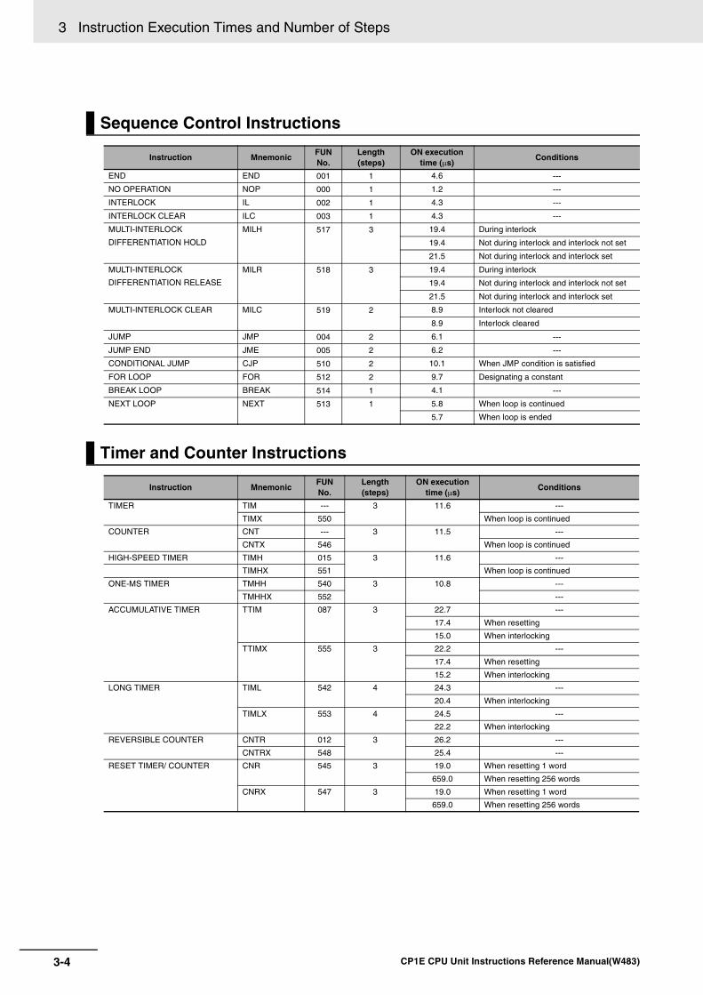
3 Instruction Execution Times and Number of Steps
Sequence Control Instructions
Instruction MnemonicFUN No.
Length (steps)
ON executiontime (µs)
Conditions
END END 001 1 4.6 ---
NO OPERATION NOP 000 1 1.2 ---
INTERLOCK IL 002 1 4.3 ---
INTERLOCK CLEAR ILC 003 1 4.3 ---
MULTI-INTERLOCK
DIFFERENTIATION HOLD
MILH 517 3 19.4 During interlock
19.4 Not during interlock and interlock not set
21.5 Not during interlock and interlock set
MULTI-INTERLOCK
DIFFERENTIATION RELEASE
MILR 518 3 19.4 During interlock
19.4 Not during interlock and interlock not set
21.5 Not during interlock and interlock set
MULTI-INTERLOCK CLEAR MILC 519 2 8.9 Interlock not cleared
8.9 Interlock cleared
JUMP JMP 004 2 6.1 ---
JUMP END JME 005 2 6.2 ---
CONDITIONAL JUMP CJP 510 2 10.1 When JMP condition is satisfied
FOR LOOP FOR 512 2 9.7 Designating a constant
BREAK LOOP BREAK 514 1 4.1 ---
NEXT LOOP NEXT 513 1 5.8 When loop is continued
5.7 When loop is ended
Timer and Counter Instructions
Instruction MnemonicFUN No.
Length (steps)
ON executiontime (µs)
Conditions
TIMER TIM --- 3 11.6 ---
TIMX 550 When loop is continued
COUNTER CNT --- 3 11.5 ---
CNTX 546 When loop is continued
HIGH-SPEED TIMER TIMH 015 3 11.6 ---
TIMHX 551 When loop is continued
ONE-MS TIMER TMHH 540 3 10.8 ---
TMHHX 552 ---
ACCUMULATIVE TIMER TTIM 087 3 22.7 ---
17.4 When resetting
15.0 When interlocking
TTIMX 555 3 22.2 ---
17.4 When resetting
15.2 When interlocking
LONG TIMER TIML 542 4 24.3 ---
20.4 When interlocking
TIMLX 553 4 24.5 ---
22.2 When interlocking
REVERSIBLE COUNTER CNTR 012 3 26.2 ---
CNTRX 548 25.4 ---
RESET TIMER/ COUNTER CNR 545 3 19.0 When resetting 1 word
659.0 When resetting 256 words
CNRX 547 3 19.0 When resetting 1 word
659.0 When resetting 256 words
3-4 CP1E CPU Unit Instructions Reference Manual(W483)

3 Instruction Execution Times and Number of Steps3-1 C
P1E
CP
U U
nit In
structio
nE
xecutio
n T
imes an
d N
um
ber o
f
3
Comparison Instructions
Instruction Mnemonic FUN No.Length (steps)
ON executiontime (µs)
Conditions
Input Comparison Instructions
(unsigned)
LD,AND,OR+= 300 4 9.3 ---
LD,AND,OR+<> 305
LD,AND,OR+< 310
LD,AND,OR+<= 315
LD,AND,OR+> 320
LD,AND,OR+>= 325
Input Comparison Instructions
(double, unsigned)
LD,AND,OR+=+L 301 4 10.8 ---
LD,AND,OR+<>+L 306
LD,AND,OR+<+L 311
LD,AND,OR+<=+L 316
LD,AND,OR+>+L 321
LD,AND,OR+>=+L 326
Input Comparison Instructions
(signed)
LD,AND,OR+=+S 302 4 9.4 ---
LD,AND,OR+<>+S 307
LD,AND,OR+<+S 312
LD,AND,OR+<=+S 317
LD,AND,OR+>+S 322
LD,AND,OR+>=+S 327
Input Comparison Instructions
(double, signed)
LD,AND,OR+=+SL 303 4 10.9 ---
LD,AND,OR+<>+SL 308
LD,AND,OR+<+SL 313
LD,AND,OR+<=+SL 318
LD,AND,OR+>+SL 323
LD,AND,OR+>=+SL 328
Time Comparison Instructions =DT 341 4 14.5 ---
<>DT 342 4 14.5 ---
<DT 343 4 14.4 ---
<=DT 344 4 14.4 ---
>DT 345 4 14.6 ---
>=DT 346 4 14.6 ---
COMPARE CMP 020 3 8.1 ---
!CMP 020 7 49.1 ---
DOUBLE COMPARE CMPL 060 3 9.5 ---
SIGNED BINARY COMPARE CPS 114 3 8.1 ---
!CPS 114 7 49.1 ---
DOUBLE SIGNED BINARY
COMPARE
CPSL 115 3 9.5 ---
TABLE COMPARE TCMP 085 4 61.1 ---
UNSIGNED BLOCK COMPARE BCMP 068 4 107.6 ---
AREA RANGE COMPARE ZCP 088 3 17.8 ---
DOUBLE AREA RANGE
COMPARE
ZCPL 116 3 20.1 ---
3-5CP1E CPU Unit Instructions Reference Manual(W483)

3 Instruction Execution Times and Number of Steps
Data Movement Instructions
Instruction MnemonicFUN No.
Length (steps)
ON executiontime (µs)
Conditions
MOVE MOV 021 3 8.0 ---
!MOV 021 7 57.7 ---
DOUBLE MOVE MOVL 498 3 8.9 ---
MOVE NOT MVN 022 3 13.7 ---
MOVE BIT MOVB 082 4 21.4 ---
MOVE DIGIT MOVD 083 4 22.4 ---
MULTIPLE BIT TRANSFER XFRB 062 26.4 Transferring 1 word
137.3 Transferring 255 bits
BLOCK TRANSFER XFER 070 4 24.2 Transferring 1 word
3747.7 Transferring 1,000 words
BLOCK SET BSET 071 4 21.3 Setting 1 word
2074.4 Setting 1,000 words
DATA EXCHANGE XCHG 073 3 19.2 ---
SINGLE WORD DISTRIBUTE DIST 080 4 20.8 ---
DATA COLLECT COLL 081 4 20.6 ---
Data Shift Instructions
Instruction MnemonicFUN No.
Length (steps)
ON executiontime (µs)
Conditions
SHIFT REGISTER SFT 010 3 14.1 Shifting 1 word
1076.0 Shifting 290 words
REVERSIBLE SHIFT REGISTER SFTR 084 4 18.0 Shifting 1 word
3784.4 Shifting 1,000 words
WORD SHIFT WSFT 016 4 25.8 Shifting 1 word
3783.9 Shifting 1,000 words
ARITHMETIC SHIFT LEFT ASL 025 2 13.0 ---
ARITHMETIC SHIFT RIGHT ASR 026 2 13.0 ---
ROTATE LEFT ROL 027 2 13.3 ---
ROTATE RIGHT ROR 028 2 13.5 ---
ONE DIGIT SHIFT LEFT SLD 074 3 21.8 Shifting 1 word
3778.3 Shifting 1,000 words
ONE DIGIT SHIFT RIGHT SRD 075 3 22.2 Shifting 1 word
3778.6 Shifting 1,000 words
SHIFT N-BITS LEFT NASL 580 3 19.5 ---
DOUBLE SHIFT NBITS LEFT NSLL 582 3 20.8 ---
SHIFT N-BITS RIGHT NASR 581 3 19.6 ---
DOUBLE SHIFT NBITS RIGHT NSRL 583 3 21.0 ---
3-6 CP1E CPU Unit Instructions Reference Manual(W483)
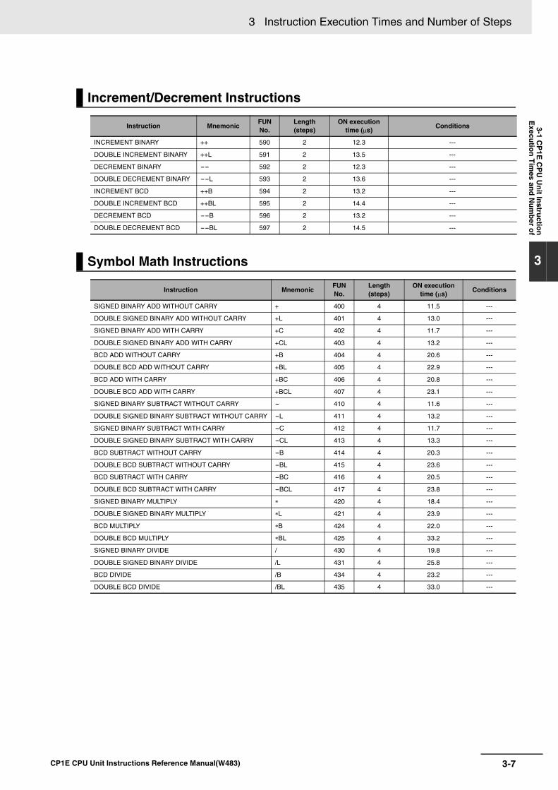
3 Instruction Execution Times and Number of Steps3-1 C
P1E
CP
U U
nit In
structio
nE
xecutio
n T
imes an
d N
um
ber o
f
3
Increment/Decrement Instructions
Instruction MnemonicFUN No.
Length (steps)
ON executiontime (µs)
Conditions
INCREMENT BINARY ++ 590 2 12.3 ---
DOUBLE INCREMENT BINARY ++L 591 2 13.5 ---
DECREMENT BINARY -- 592 2 12.3 ---
DOUBLE DECREMENT BINARY --L 593 2 13.6 ---
INCREMENT BCD ++B 594 2 13.2 ---
DOUBLE INCREMENT BCD ++BL 595 2 14.4 ---
DECREMENT BCD --B 596 2 13.2 ---
DOUBLE DECREMENT BCD --BL 597 2 14.5 ---
Symbol Math Instructions
Instruction MnemonicFUN No.
Length (steps)
ON executiontime (µs)
Conditions
SIGNED BINARY ADD WITHOUT CARRY + 400 4 11.5 ---
DOUBLE SIGNED BINARY ADD WITHOUT CARRY +L 401 4 13.0 ---
SIGNED BINARY ADD WITH CARRY +C 402 4 11.7 ---
DOUBLE SIGNED BINARY ADD WITH CARRY +CL 403 4 13.2 ---
BCD ADD WITHOUT CARRY +B 404 4 20.6 ---
DOUBLE BCD ADD WITHOUT CARRY +BL 405 4 22.9 ---
BCD ADD WITH CARRY +BC 406 4 20.8 ---
DOUBLE BCD ADD WITH CARRY +BCL 407 4 23.1 ---
SIGNED BINARY SUBTRACT WITHOUT CARRY - 410 4 11.6 ---
DOUBLE SIGNED BINARY SUBTRACT WITHOUT CARRY -L 411 4 13.2 ---
SIGNED BINARY SUBTRACT WITH CARRY -C 412 4 11.7 ---
DOUBLE SIGNED BINARY SUBTRACT WITH CARRY -CL 413 4 13.3 ---
BCD SUBTRACT WITHOUT CARRY -B 414 4 20.3 ---
DOUBLE BCD SUBTRACT WITHOUT CARRY -BL 415 4 23.6 ---
BCD SUBTRACT WITH CARRY -BC 416 4 20.5 ---
DOUBLE BCD SUBTRACT WITH CARRY -BCL 417 4 23.8 ---
SIGNED BINARY MULTIPLY ∗ 420 4 18.4 ---
DOUBLE SIGNED BINARY MULTIPLY ∗L 421 4 23.9 ---
BCD MULTIPLY ∗B 424 4 22.0 ---
DOUBLE BCD MULTIPLY ∗BL 425 4 33.2 ---
SIGNED BINARY DIVIDE / 430 4 19.8 ---
DOUBLE SIGNED BINARY DIVIDE /L 431 4 25.8 ---
BCD DIVIDE /B 434 4 23.2 ---
DOUBLE BCD DIVIDE /BL 435 4 33.0 ---
3-7CP1E CPU Unit Instructions Reference Manual(W483)

3 Instruction Execution Times and Number of Steps
Conversion Instructions
Instruction MnemonicFUN No.
Length (steps)
ON executiontime (µs)
Conditions
BCD TO BINARY BIN 023 3 15.1 ---
DOUBLE BCD TO DOUBLE BINARY
BINL 058 3 16.7 ---
BINARY TO BCD BCD 024 3 15.1 ---
DOUBLE BINARY TO
DOUBLE BCD
BCDL 059 3 17.3 ---
2’S COMPLEMENT NEG 160 3 14.3 ---
DATA DECODER MLPX 076 4 19.6 Decoding 1 digit (4 to 16)
31.0 Decoding 4 digits (4 to 16)
79.4 Decoding 1 digit (8 to 256)
138.2 Decoding 2 digits (8 to 256)
DATA ENCODER DMPX 077 4 32.5 Encoding 1 digit (16 to 4)
63.0 Encoding 4 digits (16 to 4)
68.0 Encoding 1 digit (256 to 8)
112.3 Encoding 2 digits (256 to 8)
ASCII CONVERT ASC 086 4 22.8 Converting 1 digit into ASCII
24.7 Converting 4 digits into ASCII
ASCII TO HEX HEX 162 4 18.4 Converting 1 digit
Logic Instructions
Instruction MnemonicFUN No.
Length (steps)
ON executiontime (µs)
Conditions
LOGICAL AND ANDW 034 4 18.6 ---
DOUBLE LOGICAL AND ANDL 610 4 20.4 ---
LOGICAL OR ORW 035 4 18.6 ---
DOUBLE LOGICAL OR ORWL 611 4 20.4 ---
EXCLUSIVE OR XORW 036 4 18.6 ---
DOUBLE EXCLUSIVE OR XORL 612 4 20.4 ---
COMPLEMENT COM 029 2 12.4 ---
DOUBLE COMPLEMENT COML 614 2 13.6 ---
Special Math Instructions
Instruction MnemonicFUN No.
Length (steps)
ON executiontime (µs)
Conditions
ARITHMETIC PROCESS APR 069 4 34.2 Designating SIN and COS
25.9 Designating line-segment approximation
BIT COUNTER BCNT 067 4 19.5 Counting 1 word
3-8 CP1E CPU Unit Instructions Reference Manual(W483)

3 Instruction Execution Times and Number of Steps3-1 C
P1E
CP
U U
nit In
structio
nE
xecutio
n T
imes an
d N
um
ber o
f
3
Floating-point Math Instructions
Instruction MnemonicFUN No.
Length (steps)
ON executiontime (µs)
Conditions
FLOATING TO 16-BIT FIX 450 3 15.9 ---
FLOATING TO 32-BIT FIXL 451 3 16.2 ---
16-BIT TO FLOATING FLT 452 3 16.2 ---
32-BIT TO FLOATING FLTL 453 3 17.1 ---
FLOATING-POINT ADD +F 454 4 24.1 ---
FLOATING-POINT SUBTRACT -F 455 4 25.2 ---
FLOATING-POINT DIVIDE /F 457 4 25.0 ---
FLOATING-POINT MULTIPLY ∗F 456 4 24.4 ---
Floating Symbol Comparison LD,AND,OR+=F 329 3 11.6 ---
LD,AND,OR+<>F 330 ---
LD,AND,OR+<F 331 ---
LD,AND,OR+<=F 332 ---
LD,AND,OR+>F 333 ---
LD,AND,OR+>=F 334 ---
FLOATING- POINT TO ASCII FSTR 448 4 56.8 ---
ASCII TO FLOATING-POINT FVAL 449 3 42.9 ---
Table Data Processing Instructions
Instruction MnemonicFUN No.
Length (steps)
ON executiontime (µs)
Conditions
SWAP BYTES SWAP 637 3 16.8 Swapping 1 word
6250.0 Swapping 1,000 words
FRAME CHECKSUM FCS 180 4 24.1 For 1-word table length
2710.0 For 1,000-word table length
Data Control Instructions
Instruction MnemonicFUN No.
Length (steps)
ON executiontime (µs)
Conditions
PID CONTROL WITH AUTOTUN-ING
PIDAT 191 4 316.0 Initial execution of PID processing
270.0 PID processing When sampling
228.0 PID processing When not sampling
275.5 Initial execution of autotuning
276.0 Autotuning when sampling
TIME-PROPORTIONAL OUTPUT TPO 685 4 5.8 OFF execution time
40.8 ON execution time with duty designation or displayed output limit
43.4 ON execution time with manipulated vari-able designation and output limit enabled
SCALING SCL 194 4 24.8 ---
SCALING 2 SCL2 486 4 20.2 ---
SCALING 3 SCL3 487 4 26.4 ---
AVERAGE AVG 195 4 24.2 Average of an operation
225.5 Average of 64 operations
3-9CP1E CPU Unit Instructions Reference Manual(W483)

3 Instruction Execution Times and Number of Steps
Subroutine Instructions
Instruction MnemonicFUN No.
Length (steps)
ON executiontime (µs)
Conditions
SUBROUTINE CALL SBS 091 2 6.6 ---
SUBROUTINE ENTRY SBN 092 2 2.6 ---
SUBROUTINE RETURN RET 093 1 3.1 ---
Interrupt Control Instructions
Instruction MnemonicFUN No.
Length (steps)
ON executiontime (µs)
Conditions
SET INTERRUPT MASK MSKS 690 3 15.1 Set
15.1 Reset
CLEAR INTERRUPT CLI 691 3 14.9 Set
18.0 Reset
DISABLE INTERRUPTS DI 693 1 8.5 ---
ENABLE INTERRUPTS EI 694 1 8.9 ---
High-speed Counter and Pulse Output Instructions
Instruction MnemonicFUN No.
Length (steps)
ON executiontime (µs)
Conditions
MODE CONTROL INI 880 4 46.0 Starting high-speed counter comparison
31.8 Stopping high-speed counter comparison
48.7 Changing pulse output PV
35.2 Changing high-speed counter PV
27.2 Stopping pulse output
13.0 Stopping PWM(891) output
HIGH-SPEED COUNTER PV
READ
PRV 881 4 40.0 Reading pulse output PV
35.0 Reading high-speed counter PV
37.2 Reading pulse output status
32.6 Reading high-speed counter status
24.5 Reading PWM(891) status
36.5 Reading high-speed counter range comparison results
29.1 Reading frequency of high-speed counter 0
COMPARISON TABLE LOAD CTBL 882 4 69.3 Registering target value table and starting comparison for 1 target value
116.3 Registering target value table and starting comparison for 6 target values
126.6 Registering range table and starting com-parison
46.3 Only registering target value table for 1 target value
93.3 Only registering target value table for 6target values
122.5 Only registering range table
SPEED OUTPUT SPED 885 4 69.2 Continuous mode
74.0 Independent mode
SET PULSES PULS 886 4 44.1 ---
PULSE OUTPUT PLS2 887 5 97.6 ---
3-10 CP1E CPU Unit Instructions Reference Manual(W483)

3 Instruction Execution Times and Number of Steps3-1 C
P1E
CP
U U
nit In
structio
nE
xecutio
n T
imes an
d N
um
ber o
f
3
ACCELERATION CONTROL ACC 888 4 75.6 Continuous mode
82.8 Independent mode
ORIGIN SEARCH ORG 889 3 52.2 Origin search
126.8 Origin return
PULSE WITH VARIABLE DUTYFACTOR
PWM 891 4 28.9 ---
Step Instructions
Instruction MnemonicFUN No.
Length (steps)
ON executiontime (µs)
Conditions
STEP DEFINE STEP 008 2 10.5 Step control bit ON
10.4 Step control bit OFF
STEP START SNXT 009 2 9.6 ---
I/O Unit Instructions
Instruction MnemonicFUN No.
Length (steps)
ON executiontime (µs)
Conditions
I/O REFRESH IORF097 3
170.7 Refreshing 1 input word for CP1W Expansion Unit
146.6 Refreshing 1 output word for CP1W Expansion Unit
1725.8 Refreshing 12 input words for CP1W Expansion Unit
1359.9 Refreshing 12 output words for CP1W Expansion Unit
7-SEGMENT DECODER SDEC 078 4 21.9 ---
MATRIX INPUT MTR 213 5 31.6 Data input value: 00
31.6 Data input value:FF
7-SEGMENT DISPLAY OUTPUT 7SEG 214 5 27.1 4 digits
30.8 8 digits
Serial Communications Instructions
Instruction MnemonicFUN No.
Length (steps)
ON executiontime (µs)
Conditions
TRANSMIT TXD 236 4 25.0 Sending 1 byte
25.0 Sending 256 bytes
RECEIVE RXD 235 4 39.2 Storing 1 byte
256.6 Storing 256 bytes
Clock Instructions
Instruction MnemonicFUN No.
Length (steps)
ON executiontime (µs)
Conditions
CALENDAR ADD CADD 730 4 56.6 ---
CALENDAR SUBTRACT CSUB 731 4 55.1 ---
CLOCK ADJUSTMENT DATE 735 2 29.9 ---
Instruction MnemonicFUN No.
Length (steps)
ON executiontime (µs)
Conditions
3-11CP1E CPU Unit Instructions Reference Manual(W483)

3 Instruction Execution Times and Number of Steps
Failure Diagnosis Instructions
Instruction MnemonicFUN No.
Length (steps)
ON executiontime (µs)
Conditions
FAILURE ALARM FAL 006 3 55.6 Recording errors
79.6 Deleting errors (in order of priority)
61.6 Deleting errors (all errors)
60.0 Deleting errors (individually)
SEVERE FAILURE ALARM FALS 007 3 --- ---
Other Instructions
Instruction MnemonicFUN No.
Length (steps)
ON executiontime (µs)
Conditions
SET CARRY STC 040 1 32.6 ---
CLEAR CARRY CLC 041 1 3.9 ---
EXTEND MAXIMUM CYCLE TIME WDT 094 2 11.7 ---
3-12 CP1E CPU Unit Instructions Reference Manual(W483)

44
This section describes how to monitor and calculate the cycle time of a CP1E CPU Unitthat can be used in the programs.
4-1 Monitoring the Cycle Time . . . . . . . . . . . . . . . . . . . . . . . . . . . . . . . . . . . . . . 4-24-1-1 Monitoring the Cycle Time . . . . . . . . . . . . . . . . . . . . . . . . . . . . . . . . . . . . . . . . 4-2
4-2 Computing the Cycle Time . . . . . . . . . . . . . . . . . . . . . . . . . . . . . . . . . . . . . . 4-34-2-1 CPU Unit Operation Flowchart . . . . . . . . . . . . . . . . . . . . . . . . . . . . . . . . . . . . 4-3
4-2-2 Cycle Time Overview . . . . . . . . . . . . . . . . . . . . . . . . . . . . . . . . . . . . . . . . . . . . 4-44-2-3 I/O Refresh Times for PLC Units . . . . . . . . . . . . . . . . . . . . . . . . . . . . . . . . . . . 4-54-2-4 Cycle Time Calculation Example . . . . . . . . . . . . . . . . . . . . . . . . . . . . . . . . . . . 4-6
4-2-5 Increase in Cycle Time for Online Editing . . . . . . . . . . . . . . . . . . . . . . . . . . . . 4-6
Monitoring and Computing the Cycle Time
4-1CP1E CPU Unit Instructions Reference Manual(W483)
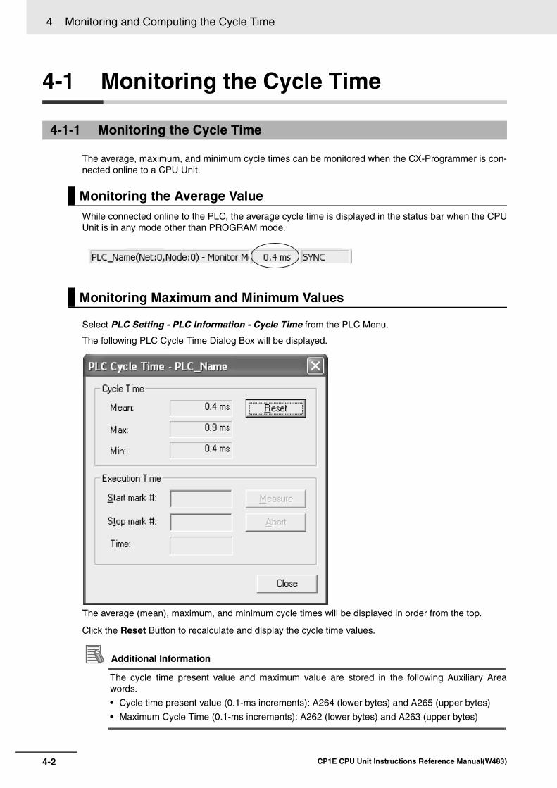
4 Monitoring and Computing the Cycle Time
4-1 Monitoring the Cycle Time
The average, maximum, and minimum cycle times can be monitored when the CX-Programmer is con-nected online to a CPU Unit.
While connected online to the PLC, the average cycle time is displayed in the status bar when the CPUUnit is in any mode other than PROGRAM mode.
Select PLC Setting - PLC Information - Cycle Time from the PLC Menu.
The following PLC Cycle Time Dialog Box will be displayed.
The average (mean), maximum, and minimum cycle times will be displayed in order from the top.
Click the Reset Button to recalculate and display the cycle time values.
Additional Information
The cycle time present value and maximum value are stored in the following Auxiliary Areawords.
• Cycle time present value (0.1-ms increments): A264 (lower bytes) and A265 (upper bytes)
• Maximum Cycle Time (0.1-ms increments): A262 (lower bytes) and A263 (upper bytes)
4-1-1 Monitoring the Cycle Time
Monitoring the Average Value
Monitoring Maximum and Minimum Values
4-2 CP1E CPU Unit Instructions Reference Manual(W483)

4 Monitoring and Computing the Cycle Time4-2 C
om
pu
ting
the C
ycle Tim
e
4
4-2-1 CP
U U
nit Operation F
lowchart
4-2 Computing the Cycle Time
The CPU Unit processes data in repeating cycles from the overseeing processing up to peripheral servicing as shown in the following diagram.
4-2-1 CPU Unit Operation Flowchart
Power ON
Check OK?
End of program?
Sets error flags
Calculates cycle time
I/O refresh I/O r
efre
sh
Peripheral servicing
NO
YES
Error
Normal
Checks Unit connection status
Checks hardware and user program memory
ERR/ALM indicator ON or flashing?
Flashing (non-fatal error)
Lit (fatal error)
Sta
rtup
initi
aliz
atio
nO
vers
eein
g pr
oces
sing
Pro
gram
exe
cutio
nC
ycle
tim
e ca
lcul
atio
n PLC
cyc
le ti
me
Per
iphe
ral
serv
icin
g
User program executedCyclic task executed
Waits until the set cycle time has elapsed (when the
minimum cycle time is valid)
4-3CP1E CPU Unit Instructions Reference Manual(W483)

4 Monitoring and Computing the Cycle Time
The cycle time depends on the following conditions.
• Type and number of instructions in the user program (cyclic tasks and all interrupt tasks for which theexecution conditions have been satisfied)
• Type and number of CP-series Expansion Units and Expansion I/O Units
• Minimum (constant) cycle time setting in the PLC Setup
• Use of peripheral USB and serial ports
Precautions for Correct UsePrecautions for Correct Use
When the mode is switched from MONITOR mode to RUN mode, the cycle time may be extendedby 10 ms (this will not, however, cause a cycle time exceeded error).
The cycle time is the total time required for the PLC to perform the operations given in the followingtables.
Cycle time = (1) + (2) + (3) + (4) + (5)
(1) Overseeing
(2) Program Execution
(3) Cycle Time Calculation for Minimum Cycle Time
(4) I/O Refreshing
(5) Peripheral Servicing
4-2-2 Cycle Time Overview
OperationProcessing time and
fluctuation cause
Checks the I/O bus and user memory, checks for battery errors, etc.
0.4 ms min.
OperationProcessing time and
fluctuation cause
Executes the instructions in the user program. The time required is the total of the executions times for all instructions.
Total instruction execution time.
Operation Processing time and fluctuation cause
Waits for the specified cycle time to elapse when a minimum (con-stant) cycle time has been set in the PLC Setup.
Calculates the cycle time.
When a minimum cycle time is not set, the time for step 3 is approximately 0.
When a minimum cycle time is set, the time for step 3 is the preset fixed cycle time minus the actual cycle time ((1) + (2) + (4) + (5)).
OperationProcessing time and
fluctuation cause
CPU Unit built-in I/O, CPU Unit built-in analog I/O (NA-type only), CP-series Expansion Units and Expansion I/O Units
Outputs from the CPU Unit to the actual outputs are refreshed first for each Unit, and then inputs.
I/O refresh time for each Unit multiplied by the number of Units used.
Operation Processing time and fluctuation cause
Services peripheral USB port In this servicing, 8% of the previous cycle’s cycle time (calcu-lated in step (3)) will be allowed for peripheral servicing.Services serial port
(Built-in RS-232C port, serial option board)
4-4 CP1E CPU Unit Instructions Reference Manual(W483)

4 Monitoring and Computing the Cycle Time4-2 C
om
pu
ting
the C
ycle Tim
e
4
4-2-3 I/O R
efresh Tim
es for PLC
Units
I/O Refresh Times for Built-in Analog I/O (NA-type CPU Unit only)
Note No matter whether use analog I/O function or not, the I/O refresh time is the same.
I/O Refresh Times for CP-series Expansion Units and Expansion I/O Units
Additional Information
The I/O refresh time for the built-in I/O of the CPU Unit is included in overseeing processing.
4-2-3 I/O Refresh Times for PLC Units
Unit name Model numbers I/O refresh time per unitNA-type CPU Unit 20-point I/O + Analog I/O
CPU UnitCP1E-NA20D- 0.5 ms
Unit name Model numbers I/O refresh time per unitExpansion I/O Unit 8-point Input Unit CP1W-8ED 0.14 ms
8-point Output Unit CP1W-8ER 0.06 msCP1W-8ETCP1W-8ET1
16-point Output Unit CP1W-16ER 0.17 msCP1W-16ETCP1W-16ET1
20-point I/O Unit CP1W-20EDR1 0.20 msCP1W-20EDTCP1W-20EDT1
32-point Output Unit CP1W-32ER 0.33 msCP1W-32ETCP1W-32ET1
40-point I/O Unit CP1W-40EDR 0.45 msCP1W-40EDTCP1W-40EDT1
Expansion Unit Analog Input Unit CP1W-AD041 0.72 msCP1W-AD042 0.87 ms
Analog Output Unit CP1W-DA021 0.33 msCP1W-DA041CP1W-DA042 0.40 ms
Analog I/O Units CP1W-MAD11 0.36 msCP1W-MAD42 0.87 msCP1W-MAD44 0.97 ms
Temperature Sensor Unit CP1W-TS001 0.30 msCP1W-TS002 0.57 msCP1W-TS003 0.67 msCP1W-TS004 0.47 msCP1W-TS101 0.30 msCP1W-TS102 0.57 ms
CompoBus/S I/O Link Unit CP1W-SRT21 0.20 ms
4-5CP1E CPU Unit Instructions Reference Manual(W483)

4 Monitoring and Computing the Cycle Time
The following example shows the method used to calculate the cycle time when Expansion I/O Unitsare connected to a CP1E CPU Unit.
Conditions
Calculation Example
When online editing is executed to change the program from the CX-Programmer while the CPU Unit isoperating in MONITOR mode, the CPU Unit will momentarily suspend operation while the program isbeing changed. The cycle time is extended by the writing programs for the CPU Unit. And the scheduletask will not be executed while the CPU Unit suspends operation.
If the program size is 8K steps, the cycle time extension will be as follows:
When editing online, the cycle time will be extended and the schedule task execution may be delayed orbecome abnormal according to the editing that is performed.
4-2-4 Cycle Time Calculation Example
Item Description
CP1E CPU Unit 40-point I/O Unit
CP1W-40EDR
1 Unit
Ladder diagram 5K steps LD instructions: 2.5K steps
OUT instructions: 2.5K steps
Peripheral USB port connection Yes or no
Minimum cycle time processing None
Serial port connection None
Other peripheral servicing None
Process name Equation
Processing time
Peripheral USB port connected
Peripheral USB port not
connected
(1)Overseeing − 0.4 ms 0.4 ms
(2)Program execution 1.19µs×2,500+1.61µs×2,500 7.0 ms 7.0 ms
(3)Cycle time calculation (Minimum cycle time not set.) 0 ms 0 ms
(4)I/O refreshing 0.45 ms 0.45 ms 0.45 ms
(5)Peripheral servicing (Only peripheral USB port connected) 0.2 ms 0 ms
Cycle time (1)+(2)+(3)+(4)+(5) 8.15 ms 7.85 ms
4-2-5 Increase in Cycle Time for Online Editing
CPU Unit Increase in cycle time for online editing
CP1E CPU Unit Maximum: 16 ms, Normal: 6 ms (for a program size of 8K steps)
4-6 CP1E CPU Unit Instructions Reference Manual(W483)

App
Ap
p
Alphabetical List of Instructions by Mnemonic . . . . . . . . . . . . . . . . . . . . . . . . . . A-2
Appendices
A-1CP1E CPU Unit Instructions Reference Manual(W483)

Appendices
Alphabetical List of Instructions by Mnemonic
A
Mne-monic
InstructionFUN No.
Upward differen-tiation
Downward differentia-
tion
Immediate refreshing specifica-
tion
Page
ACC ACCELER-ATION CONTROL
888 @ACC --- --- 2-331
AND AND --- @AND %AND !AND 2-9
ANDLD
AND LOAD --- --- --- --- 2-13
AND NOT
AND NOT --- --- --- !AND NOT
2-9
AND< AND LESS THAN
310 --- --- --- 2-88
AND<= AND LESS THAN OR EQUAL
315 --- --- --- 2-88
AND<=F AND FLOATING LESS THAN OR EQUAL
332 --- --- --- 2-241
AND<=DT
AND TIME LESS THAN OR EQUAL
344 --- --- --- 2-91
AND<=L AND DOU-BLE LESS THAN OR EQUAL
316 --- --- --- 2-88
AND<=S AND SIGNED LESS THAN OR EQUAL
317 --- --- --- 2-88
AND<=SL
AND DOU-BLE SIGNED LESS THAN OR EQUAL
318 --- --- --- 2-88
AND<> AND NOT EQUAL
305 --- --- --- 2-88
AND<>DT
AND TIME NOT EQUAL
342 --- --- --- 2-91
AND<>F AND FLOATING NOT EQUAL
330 --- --- --- 2-241
AND<>L AND DOU-BLE NOT EQUAL
306 --- --- --- 2-88
AND<>S AND SIGNED NOT EQUAL
307 --- --- --- 2-88
AND<>SL
AND DOU-BLE SIGNED NOT EQUAL
308 --- --- --- 2-88
AND<DT
AND TIME LESS THAN
343 --- --- --- 2-91
AND<F AND FLOATING LESS THAN
331 --- --- --- 2-241
AND<L AND DOU-BLE LESS THAN
311 --- --- --- 2-88
AND<S AND SIGNED LESS THAN
312 --- --- --- 2-88
AND<SL
AND DOU-BLE SIGNED LESS THAN
313 --- --- --- 2-88
AND= AND EQUAL
300 --- --- --- 2-88
AND=DT
AND TIME EQUAL
341 --- --- --- 2-91
AND=F AND FLOATING EQUAL
329 --- --- --- 2-241
AND=L AND DOU-BLE EQUAL
301 --- --- --- 2-88
AND=S AND SIGNED EQUAL
302 --- --- --- 2-88
AND=SL
AND DOU-BLE SIGNED EQUAL
303 --- --- --- 2-88
AND> AND GREATER THAN
320 --- --- --- 2-88
AND>= AND GREATER THAN OR EQUAL
325 --- --- --- 2-88
AND>=DT
AND TIME GREATER THAN OR EQUAL
346 --- --- --- 2-91
AND>=F AND FLOATING GREATER THAN OR EQUAL
334 --- --- --- 2-241
AND>=L AND DOU-BLE GREATER THAN OR EQUAL
326 --- --- --- 2-88
AND>=S AND SIGNED GREATER THAN OR EQUAL
327 --- --- --- 2-88
Mne-monic
InstructionFUN No.
Upward differen-tiation
Downward differentia-
tion
Immediate refreshing specifica-
tion
Page
A-2 CP1E CPU Unit Instructions Reference Manual(W483)

Appendices A
lph
abetical L
ist of In
structio
ns by M
nem
on
icA
pp
B
C
AND>=SL
AND DBL SIGNED GREATER THAN OR EQUAL
328 --- --- --- 2-88
AND>DT
AND TIME GREATER THAN
345 --- --- --- 2-91
AND>F AND FLOATING GREATER THAN
333 --- --- --- 2-241
AND>L AND DOU-BLE GREATER THAN
321 --- --- --- 2-88
AND>S AND SIGNED GREATER THAN
322 --- --- --- 2-88
AND>SL
AND DOU-BLE SIGNED GREATER THAN
323 --- --- --- 2-88
ANDL DOUBLE LOGICAL AND
610 @ANDL --- --- 2-210
ANDW LOGICAL AND
034 @ANDW --- --- 2-210
APR ARITH-METIC PROCESS
069 @APR --- --- 2-218
ASC ASCII CON-VERT
086 @ASC --- --- 2-201
ASL ARITH-METIC SHIFT LEFT
025 @ASL --- --- 2-133
ASR ARITH-METIC SHIFT RIGHT
026 @ASR --- --- 2-134
AVG AVERAGE 195 --- --- --- 2-287
Mne-monic
InstructionFUN No.
Upward differen-tiation
Downward differentia-
tion
Immediate refreshing specifica-
tion
Page
BCD BINARY TO BCD
024 @BCD --- --- 2-187
BCDL DOUBLE BINARY TO DOUBLE BCD
059 @BCDL --- --- 2-187
BCMP BLOCK COMPARE
068 @BCMP --- --- 2-103
BCNT BIT COUNTER
067 @BCNT --- --- 2-227
BIN BCD TO BINARY
023 @BIN --- --- 2-185
Mne-monic
InstructionFUN No.
Upward differen-tiation
Downward differentia-
tion
Immediate refreshing specifica-
tion
Page
BINL DOUBLE BCD TO DOUBLE BINARY
058 @BINL --- --- 2-185
BREAK BREAK LOOP
514 --- --- --- 2-59
BSET BLOCK SET 071 @BSET --- --- 2-119
Mne-monic
InstructionFUN No.
Upward differen-tiation
Downward differentia-
tion
Immediate refreshing specifica-
tion
Page
CADD CALEN-DAR ADD
730 @CADD --- --- 2-380
CJP CONDI-TIONAL JUMP
510 --- --- --- 2-53
CLC CLEAR CARRY
041 @CLC --- --- 2-398
CLI CLEAR INTER-RUPT
691 @CLI --- --- 2-303
CMP COMPARE 020 --- --- !CMP 2-95
CMPL DOUBLE COMPARE
060 --- --- --- 2-95
CNR RESET TIMER/COUNTER
545 @CNR --- --- 2-86
CNRX RESET TIMER/COUNTER
547 @CNRX --- --- 2-86
CNT COUNTER --- --- --- --- 2-80
CNTR REVERS-IBLE COUNTER
012 --- --- --- 2-83
CNTRX REVERS-IBLE COUNTER
548 --- --- --- 2-83
CNTX COUNTER 546 --- --- --- 2-80
COLL DATA COL-LECT
081 @COLL --- --- 2-125
COM COMPLE-MENT
029 @COM --- --- 2-216
COML DOUBLE COMPLE-MENT
614 @COML --- --- 2-216
CPS SIGNED BINARY COMPARE
114 --- --- !CPS 2-98
CPSL DOUBLE SIGNED BINARY-COMPARE
115 --- --- --- 2-98
CSUB CALEN-DAR SUB-TRACT
731 @CSUB --- --- 2-380
CTBL REGISTER-COMPARI-SON TABLE
882 @CTBL --- --- 2-315
Mne-monic
InstructionFUN No.
Upward differen-tiation
Downward differentia-
tion
Immediate refreshing specifica-
tion
Page
A-3CP1E CPU Unit Instructions Reference Manual(W483)

Appendices
D
E
F
H
I
J
K
L
Mne-monic
InstructionFUN No.
Upward differen-tiation
Downward differentia-
tion
Immediate refreshing specifica-
tion
Page
DATE CLOCK ADJUST-MENT
735 @DATE --- --- 2-385
DI DISABLE INTER-RUPTS
693 @DI --- --- 2-306
DIFD DIFFEREN-TIATE DOWN
014 --- --- !DIFD 2-27
DIFU DIFFEREN-TIATE UP
013 --- --- !DIFU 2-25
DIST SINGLE WORD DIS-TRIBUTE
080 @DIST --- --- 2-123
DMPX DATA ENCODER
077 @DMPX --- --- 2-196
DOWN CONDI-TION OFF
522 --- --- --- 2-17
DSW DIGITAL SWITCH INPUT
210 --- --- --- 2-357
Mne-monic
InstructionFUN No.
Upward differen-tiation
Downward differentia-
tion
Immediate refreshing specifica-
tion
Page
EI ENABLE INTER-RUPTS
694 --- --- --- 2-307
END END 001 --- --- --- 2-38
Mne-monic
InstructionFUN No.
Upward differen-tiation
Downward differentia-
tion
Immediate refreshing specifica-
tion
Page
FAL FAILURE ALARM
006 @FAL --- --- 2-387
FALS SEVERE FAILURE ALARM
007 --- --- --- 2-393
FCS FRAME CHECK-SUM
180 @FCS --- --- 2-255
FIX FLOATING TO 16-BIT
450 @FIX --- --- 2-233
FIXL FLOATING TO 32-BIT
451 @FIXL --- --- 2-233
FLT 16-BIT TO FLOATING
452 @FLT --- --- 2-235
FLTL 32-BIT TO FLOATING
453 @FLTL --- --- 2-235
FOR --- 512 --- --- --- 2-56
FSTR FLOATING-POINT TO ASCII
448 @FSTR --- --- 2-244
FVAL ASCII TO FLOATING-POINT
449 @FVAL --- --- 2-249
Mne-monic
InstructionFUN No.
Upward differen-tiation
Downward differentia-
tion
Immediate refreshing specifica-
tion
Page
HEX ASCII TO HEX
162 @HEX --- --- 2-205
Mne-monic
InstructionFUN No.
Upward differen-tiation
Downward differentia-
tion
Immediate refreshing specifica-
tion
Page
INI MODE CONTROL
880 @INI --- --- 2-308
IORF I/O REFRESH
097 @IORF --- --- 2-352
Mne-monic
InstructionFUN No.
Upward differen-tiation
Downward differentia-
tion
Immediate refreshing specifica-
tion
Page
JME JUMP END 005 --- --- --- 2-53
JMP JUMP 004 --- --- --- 2-53
Mne-monic
InstructionFUN No.
Upward differen-tiation
Downward differentia-
tion
Immediate refreshing specifica-
tion
Page
KEEP KEEP 011 --- --- !KEEP 2-21
Mne-monic
InstructionFUN No.
Upward differen-tiation
Downward differentia-
tion
Immediate refreshing specifica-
tion
Page
LD LOAD --- @LD %LD !LD 2-7
LD=DT LOAD DATE EQUAL
341 --- --- --- 2-91
LD =S LOAD SIGNED EQUAL
302 --- --- --- 2-88
Mne-monic
InstructionFUN No.
Upward differen-tiation
Downward differentia-
tion
Immediate refreshing specifica-
tion
Page
A-4 CP1E CPU Unit Instructions Reference Manual(W483)
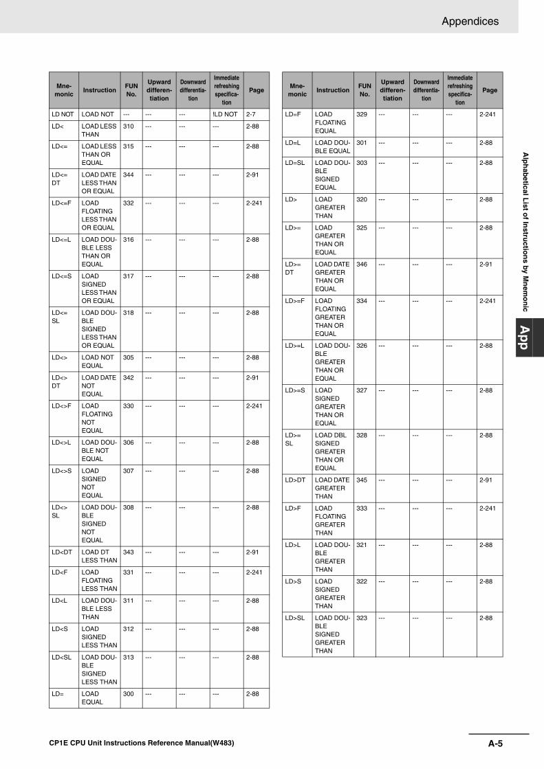
Appendices A
lph
abetical L
ist of In
structio
ns by M
nem
on
icA
pp
LD NOT LOAD NOT --- --- --- !LD NOT 2-7
LD< LOAD LESS THAN
310 --- --- --- 2-88
LD<= LOAD LESS THAN OR EQUAL
315 --- --- --- 2-88
LD<=DT
LOAD DATE LESS THAN OR EQUAL
344 --- --- --- 2-91
LD<=F LOAD FLOATING LESS THAN OR EQUAL
332 --- --- --- 2-241
LD<=L LOAD DOU-BLE LESS THAN OR EQUAL
316 --- --- --- 2-88
LD<=S LOAD SIGNED LESS THAN OR EQUAL
317 --- --- --- 2-88
LD<=SL
LOAD DOU-BLE SIGNED LESS THAN OR EQUAL
318 --- --- --- 2-88
LD<> LOAD NOT EQUAL
305 --- --- --- 2-88
LD<>DT
LOAD DATE NOT EQUAL
342 --- --- --- 2-91
LD<>F LOAD FLOATING NOT EQUAL
330 --- --- --- 2-241
LD<>L LOAD DOU-BLE NOT EQUAL
306 --- --- --- 2-88
LD<>S LOAD SIGNED NOT EQUAL
307 --- --- --- 2-88
LD<>SL
LOAD DOU-BLE SIGNED NOT EQUAL
308 --- --- --- 2-88
LD<DT LOAD DT LESS THAN
343 --- --- --- 2-91
LD<F LOAD FLOATING LESS THAN
331 --- --- --- 2-241
LD<L LOAD DOU-BLE LESS THAN
311 --- --- --- 2-88
LD<S LOAD SIGNED LESS THAN
312 --- --- --- 2-88
LD<SL LOAD DOU-BLE SIGNED LESS THAN
313 --- --- --- 2-88
LD= LOAD EQUAL
300 --- --- --- 2-88
Mne-monic
InstructionFUN No.
Upward differen-tiation
Downward differentia-
tion
Immediate refreshing specifica-
tion
Page
LD=F LOAD FLOATING EQUAL
329 --- --- --- 2-241
LD=L LOAD DOU-BLE EQUAL
301 --- --- --- 2-88
LD=SL LOAD DOU-BLE SIGNED EQUAL
303 --- --- --- 2-88
LD> LOAD GREATER THAN
320 --- --- --- 2-88
LD>= LOAD GREATER THAN OR EQUAL
325 --- --- --- 2-88
LD>=DT
LOAD DATE GREATER THAN OR EQUAL
346 --- --- --- 2-91
LD>=F LOAD FLOATING GREATER THAN OR EQUAL
334 --- --- --- 2-241
LD>=L LOAD DOU-BLE GREATER THAN OR EQUAL
326 --- --- --- 2-88
LD>=S LOAD SIGNED GREATER THAN OR EQUAL
327 --- --- --- 2-88
LD>=SL
LOAD DBL SIGNED GREATER THAN OR EQUAL
328 --- --- --- 2-88
LD>DT LOAD DATE GREATER THAN
345 --- --- --- 2-91
LD>F LOAD FLOATING GREATER THAN
333 --- --- --- 2-241
LD>L LOAD DOU-BLE GREATER THAN
321 --- --- --- 2-88
LD>S LOAD SIGNED GREATER THAN
322 --- --- --- 2-88
LD>SL LOAD DOU-BLE SIGNED GREATER THAN
323 --- --- --- 2-88
Mne-monic
InstructionFUN No.
Upward differen-tiation
Downward differentia-
tion
Immediate refreshing specifica-
tion
Page
A-5CP1E CPU Unit Instructions Reference Manual(W483)
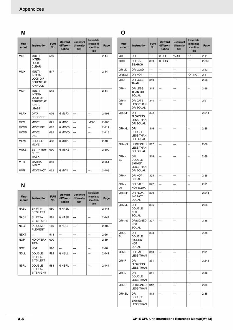
Appendices
M
N
O
Mne-monic
InstructionFUN No.
Upward differen-tiation
Downward differentia-
tion
Immediate refreshing specifica-
tion
Page
MILC MULTI-INTER-LOCK CLEAR
519 --- --- --- 2-44
MILH MULTI-INTER-LOCK DIF-FERENTIATIONHOLD
517 --- --- --- 2-44
MILR MULTI-INTER-LOCK DIF-FERENTIATIONRE-LEASE
518 --- --- --- 2-44
MLPX DATA DECODER
076 @MLPX --- --- 2-191
MOV MOVE 021 @MOV --- !MOV 2-108
MOVB MOVE BIT 082 @MOVB --- --- 2-111
MOVD MOVE DIGIT
083 @MOVD --- --- 2-113
MOVL DOUBLE MOVE
498 @MOVL --- --- 2-108
MSKS SET INTER-RUPT MASK
690 @MSKS --- --- 2-300
MTR MATRIX INPUT
213 --- --- --- 2-361
MVN MOVE NOT 022 @MVN --- --- 2-108
Mne-monic
InstructionFUN No.
Upward differen-tiation
Downward differentia-
tion
Immediate refreshing specifica-
tion
Page
NASL SHIFT N-BITS LEFT
580 @NASL --- --- 2-141
NASR SHIFT N-BITS RIGHT
581 @NASR --- --- 2-144
NEG 2'S COM-PLEMENT
160 @NEG --- --- 2-189
NEXT --- 513 --- --- --- 2-56
NOP NO OPERA-TION
000 --- --- --- 2-39
NOT NOT 520 --- --- --- 2-16
NSLL DOUBLE SHIFT N-BITS LEFT
582 @NSLL --- --- 2-141
NSRL DOUBLE SHIFT N-BITSRIGHT
583 @NSRL --- --- 2-144
Mne-monic
InstructionFUN No.
Upward differen-tiation
Downward differentia-
tion
Immediate refreshing specifica-
tion
Page
OR OR --- @OR %OR !OR 2-11
ORG ORIGIN SEARCH
889 @ORG --- --- 2-336
OR LD OR LOAD --- --- --- --- 2-13
OR NOT OR NOT --- --- --- !OR NOT 2-11
OR< OR LESS THAN
310 --- --- --- 2-88
OR<= OR LESS THAN OR EQUAL
315 --- --- --- 2-88
OR<=DT
OR DATE LESS THAN OR EQUAL
344 --- --- --- 2-91
OR<=F OR FLOATING LESS THAN OR EQUAL
332 --- --- --- 2-241
OR<=L OR DOUBLE LESS THAN OR EQUAL
316 --- --- --- 2-88
OR<=S OR SIGNED LESS THAN OR EQUAL
317 --- --- --- 2-88
OR<=SL
OR DOUBLE SIGNED LESS THAN OR EQUAL
318 --- --- --- 2-88
OR<> OR NOT EQUAL
305 --- --- --- 2-88
OR<>DT
OR DATE NOT EQUA
342 --- --- --- 2-91
OR<>F OR FLOAT-ING NOT EQUAL
330 --- --- --- 2-241
OR<>L OR DOUBLE NOT EQUAL
306 --- --- --- 2-88
OR<>S OR SIGNED NOT EQUAL
307 --- --- --- 2-88
OR<>SL
OR DOUBLE SIGNED NOT EQUAL
308 --- --- --- 2-88
OR<DT OR DATE LESS THAN
343 --- --- --- 2-91
OR<F OR FLOATING LESS THAN
331 --- --- --- 2-241
OR<L OR DOUBLE LESS THAN
311 --- --- --- 2-88
OR<S OR SIGNED LESS THAN
312 --- --- --- 2-88
OR<SL OR DOUBLE SIGNED LESS THAN
313 --- --- --- 2-88
A-6 CP1E CPU Unit Instructions Reference Manual(W483)

Appendices A
lph
abetical L
ist of In
structio
ns by M
nem
on
icA
pp
P
R
OR= OR EQUAL 300 --- --- --- 2-88
OR=DT OR DATE EQUAL
341 --- --- --- 2-91
OR=F OR FLOATING EQUAL
329 --- --- --- 2-241
OR=L OR DOUBLE EQUAL
301 --- --- --- 2-88
OR=S OR SIGNED EQUAL
302 --- --- --- 2-88
OR=SL OR DOU-BLE SIGNED EQUAL
303 --- --- --- 2-88
OR> OR GREATER THAN
320 --- --- --- 2-88
OR>= OR GREATER THAN OR EQUAL
325 --- --- --- 2-88
OR>=DT
OR DATE GREATER THAN OR EQUAL
346 --- --- --- 2-91
OR>=F OR FLOATING GREATER THAN OR EQUAL
334 --- --- --- 2-241
OR>=L OR DOUBLE GREATER THAN OR EQUAL
326 --- --- --- 2-88
OR>=S OR SIGNED GREATER THAN OR EQUAL
327 --- --- --- 2-88
OR>=SL
OR DBL SIGNED GREATER THAN OR EQUAL
328 --- --- --- 2-88
OR>DT OR DATE GREATER THAN
345 --- --- --- 2-91
OR>F OR FLOAT-ING GREATER THAN
333 --- --- --- 2-241
OR>L OR DOUBLE GREATER THAN
321 --- --- --- 2-88
OR>S OR SIGNED GREATER THAN
322 --- --- --- 2-88
OR>SL OR DOUBLE SIGNED GREATER THAN
323 --- --- --- 2-88
ORW LOGICAL OR
035 @ORW --- --- 2-212
Mne-monic
InstructionFUN No.
Upward differen-tiation
Downward differentia-
tion
Immediate refreshing specifica-
tion
Page
ORWL DOUBLE LOGICAL OR
611 @ORWL --- --- 2-212
OUT OUTPUT --- --- --- !OUT 2-18
OUT NOT
OUTPUT NOT
--- --- --- !OUT NOT
2-18
Mne-monic
InstructionFUN No.
Upward differen-tiation
Downward differentia-
tion
Immediate refreshing specifica-
tion
Page
PIDAT PID CON-TROL WITHAUTO-TUNING
191 --- --- --- 2-257
PLS2 PULSE OUTPUT
887 @PLS2 --- --- 2-325
PRV HIGH-SPEED-COUNTER PV READ
881 @PRV --- --- 2-311
PULS SET PULSES
886 @PULS --- --- 2-323
PWM PULSE WITH VARI-ABLEDUTY FACTOR
891 @PWM --- --- 2-339
Mne-monic
InstructionFUN No.
Upward differen-tiation
Downward differentia-
tion
Immediate refreshing specifica-
tion
Page
RET SUBROU-TINE RETURN
093 --- --- --- 2-295
ROL ROTATE LEFT
027 @ROL --- --- 2-135
ROR ROTATE RIGHT
028 @ROR --- --- 2-137
RSET RESET --- @RSET %RSET !RSET 2-29
RSTA MULTIPLE BIT RESET
531 @RSTA --- --- 2-31
RSTB SINGLE BIT RESET
533 @RSTB --- !RSTB 2-33
RXD RECEIVE 235 @RXD --- --- 2-374
Mne-monic
InstructionFUN No.
Upward differen-tiation
Downward differentia-
tion
Immediate refreshing specifica-
tion
Page
A-7CP1E CPU Unit Instructions Reference Manual(W483)
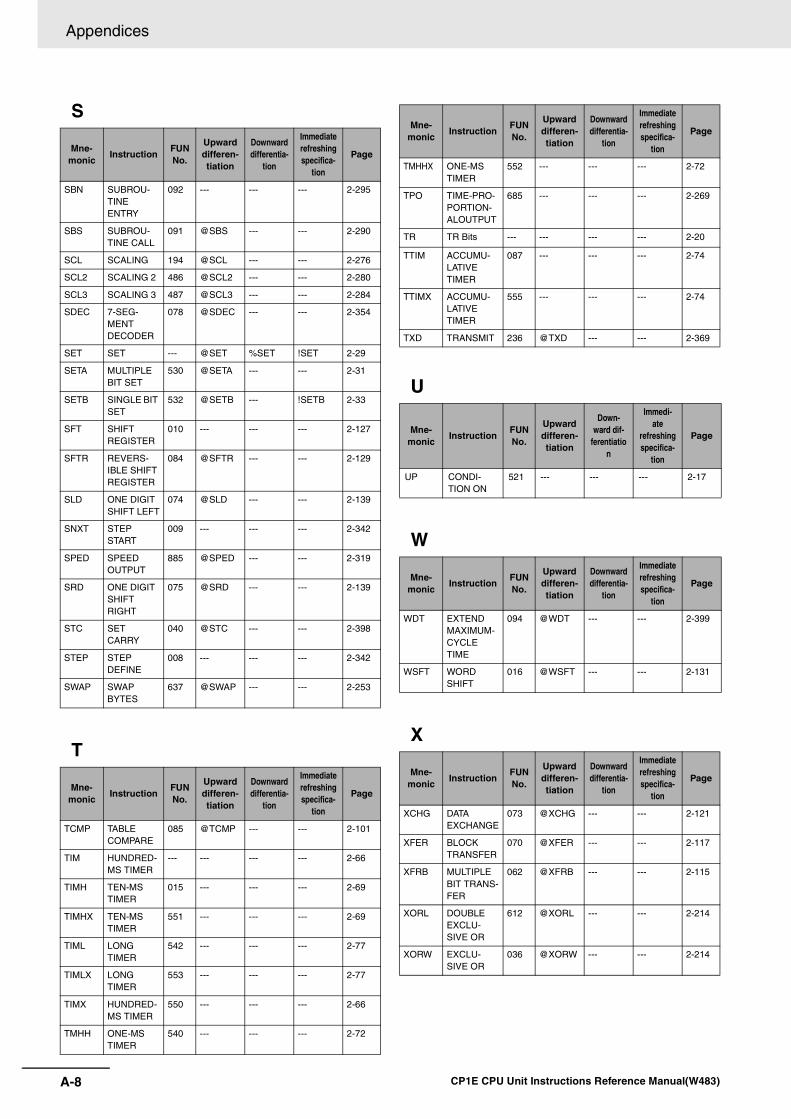
Appendices
S
T
U
W
X
Mne-monic
InstructionFUN No.
Upward differen-tiation
Downward differentia-
tion
Immediate refreshing specifica-
tion
Page
SBN SUBROU-TINE ENTRY
092 --- --- --- 2-295
SBS SUBROU-TINE CALL
091 @SBS --- --- 2-290
SCL SCALING 194 @SCL --- --- 2-276
SCL2 SCALING 2 486 @SCL2 --- --- 2-280
SCL3 SCALING 3 487 @SCL3 --- --- 2-284
SDEC 7-SEG-MENT DECODER
078 @SDEC --- --- 2-354
SET SET --- @SET %SET !SET 2-29
SETA MULTIPLE BIT SET
530 @SETA --- --- 2-31
SETB SINGLE BIT SET
532 @SETB --- !SETB 2-33
SFT SHIFT REGISTER
010 --- --- --- 2-127
SFTR REVERS-IBLE SHIFT REGISTER
084 @SFTR --- --- 2-129
SLD ONE DIGIT SHIFT LEFT
074 @SLD --- --- 2-139
SNXT STEP START
009 --- --- --- 2-342
SPED SPEED OUTPUT
885 @SPED --- --- 2-319
SRD ONE DIGIT SHIFT RIGHT
075 @SRD --- --- 2-139
STC SET CARRY
040 @STC --- --- 2-398
STEP STEP DEFINE
008 --- --- --- 2-342
SWAP SWAP BYTES
637 @SWAP --- --- 2-253
Mne-monic
InstructionFUN No.
Upward differen-tiation
Downward differentia-
tion
Immediate refreshing specifica-
tion
Page
TCMP TABLE COMPARE
085 @TCMP --- --- 2-101
TIM HUNDRED-MS TIMER
--- --- --- --- 2-66
TIMH TEN-MS TIMER
015 --- --- --- 2-69
TIMHX TEN-MS TIMER
551 --- --- --- 2-69
TIML LONG TIMER
542 --- --- --- 2-77
TIMLX LONG TIMER
553 --- --- --- 2-77
TIMX HUNDRED-MS TIMER
550 --- --- --- 2-66
TMHH ONE-MS TIMER
540 --- --- --- 2-72
TMHHX ONE-MS TIMER
552 --- --- --- 2-72
TPO TIME-PRO-PORTION-ALOUTPUT
685 --- --- --- 2-269
TR TR Bits --- --- --- --- 2-20
TTIM ACCUMU-LATIVE TIMER
087 --- --- --- 2-74
TTIMX ACCUMU-LATIVE TIMER
555 --- --- --- 2-74
TXD TRANSMIT 236 @TXD --- --- 2-369
Mne-monic
InstructionFUN No.
Upward differen-tiation
Down-ward dif-
ferentiation
Immedi-ate
refreshing specifica-
tion
Page
UP CONDI-TION ON
521 --- --- --- 2-17
Mne-monic
InstructionFUN No.
Upward differen-tiation
Downward differentia-
tion
Immediate refreshing specifica-
tion
Page
WDT EXTEND MAXIMUM-CYCLE TIME
094 @WDT --- --- 2-399
WSFT WORD SHIFT
016 @WSFT --- --- 2-131
Mne-monic
InstructionFUN No.
Upward differen-tiation
Downward differentia-
tion
Immediate refreshing specifica-
tion
Page
XCHG DATA EXCHANGE
073 @XCHG --- --- 2-121
XFER BLOCK TRANSFER
070 @XFER --- --- 2-117
XFRB MULTIPLE BIT TRANS-FER
062 @XFRB --- --- 2-115
XORL DOUBLE EXCLU-SIVE OR
612 @XORL --- --- 2-214
XORW EXCLU-SIVE OR
036 @XORW --- --- 2-214
Mne-monic
InstructionFUN No.
Upward differen-tiation
Downward differentia-
tion
Immediate refreshing specifica-
tion
Page
A-8 CP1E CPU Unit Instructions Reference Manual(W483)

Appendices A
lph
abetical L
ist of In
structio
ns by M
nem
on
icA
pp
Z
Symbol
Mne-monic
InstructionFUN No.
Upward differen-tiation
Downward differentia-
tion
Immediate refreshing specifica-
tion
Page
ZCP AREA RANGE COM-PARE
088 --- --- --- 2-105
ZCPL DOUBLE AREA RANGE-COMPARE
116 --- --- --- 2-105
Mne-monic
InstructionFUN No.
Upward differen-tiation
Downward differentia-
tion
Immediate refreshing specifica-
tion
Page
7SEG 7-SEG-MENT DIS-PLAY OUTPU
214 --- --- --- 2-365
+ SIGNED BINARY ADDWITH-OUT CARRY
400 @+ --- --- 2-158
++ INCRE-MENT BINARY
590 @++ --- --- 2-147
++B INCRE-MENT BCD
594 @++B --- --- 2-153
++BL DOUBLE INCRE-MENT BCD
595 @++BL --- --- 2-153
++L DOUBLE INCRE-MENTBI-NARY
591 @++L --- --- 2-147
+B BCD ADD WITHOUT CARRY
404 @+B --- --- 2-162
+BC BCD ADD WITH CARRY
406 @+BC --- --- 2-164
+BCL DOUBLE BCD ADD WITH-CARRY
407 @+BCL --- --- 2-164
+BL DOUBLE BCD ADD WITHOUT-CARRY
405 @+BL --- --- 2-162
+C SIGNED BINARY ADD WITH-CARRY
402 @+C --- --- 2-160
+CL DOUBLE SIGNED BINARY-ADD WITH CARRY
403 @+CL --- --- 2-160
+F FLOATING-POINT ADD
454 @+F --- --- 2-237
+L DOUBLE SIGNED BINARY-ADD WITH-OUT CARRY
401 @+L --- --- 2-158
- SIGNED BINARY SUB-TRACTWITHOUT CARRY
410 @- --- --- 2-166
-- DECRE-MENT BINARY
592 @-- --- --- 2-150
--B DECRE-MENT BCD
596 @--B --- --- 2-156
--BL DOUBLE DECRE-MENT BCD
597 @--BL --- --- 2-156
--L DECRE-MENT BINARY
593 @--L --- --- 2-150
-B BCD SUB-TRACT WITHOUT-CARRY
414 @-B --- --- 2-172
-BC BCD SUB-TRACT WITH-CARRY
416 @-BC --- --- 2-175
-BCL DOUBLE BCD SUB-TRACTWITH CARRY
417 @-BCL --- --- 2-175
-BL DOUBLE BCD SUB-TRACTWITHOUT CARRY
415 @-BL --- --- 2-172
-C SIGNED BINARY SUB-TRACTWITH CARRY
412 @-C --- --- 2-170
-CL DOUBLE SIGNED BINA-RYSUB-TRACT WITH CARRY
413 @-CL --- --- 2-170
-F FLOATING-POINT SUBTRACT
455 @-F --- --- 2-237
-L DOUBLE SIGNED BINA-RYSUB-TRACT WITHOUT-CARRY
411 @-L --- --- 2-166
* SIGNED BINARY MULTIPLY
420 @* --- --- 2-177
*B BCD MULTI-PLY
424 @*B --- --- 2-179
Mne-monic
InstructionFUN No.
Upward differen-tiation
Downward differentia-
tion
Immediate refreshing specifica-
tion
Page
A-9CP1E CPU Unit Instructions Reference Manual(W483)
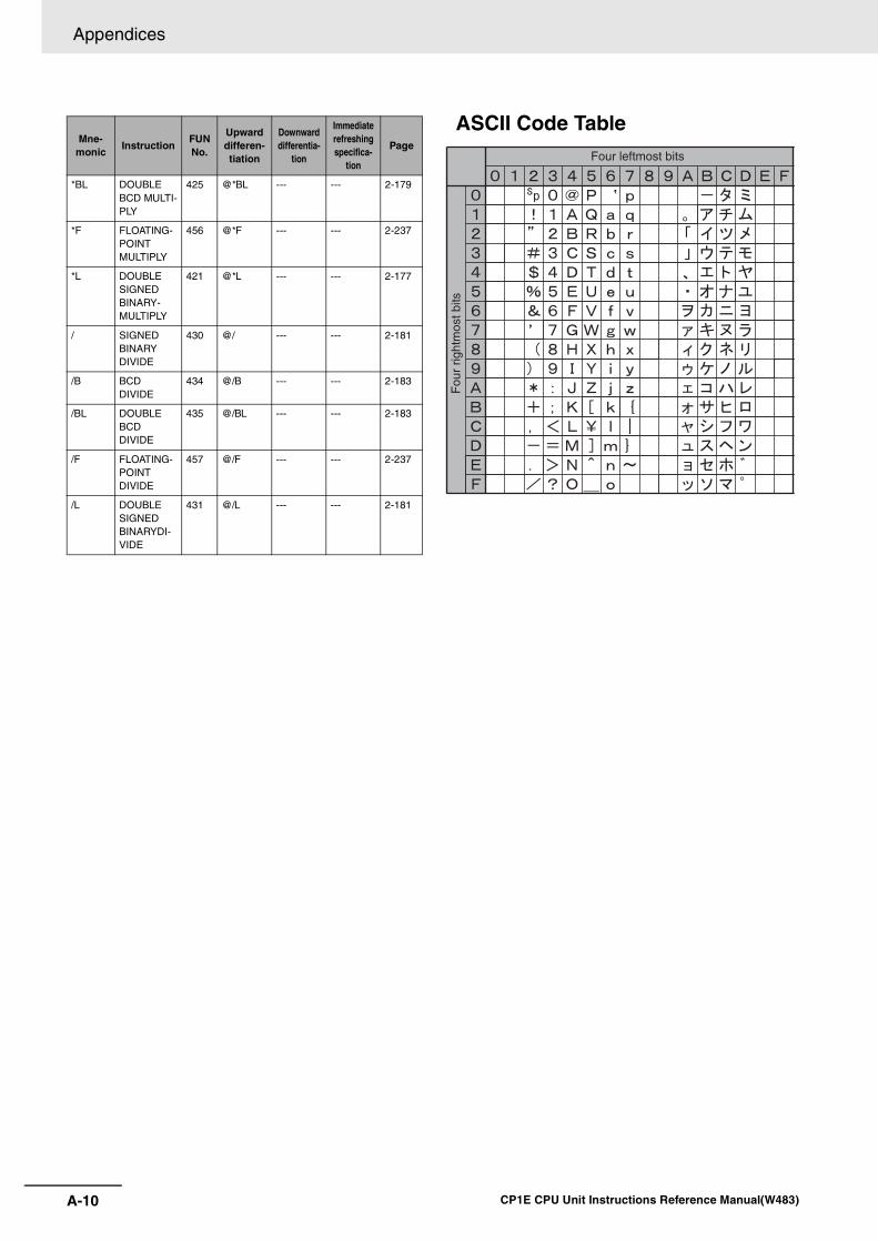
Appendices
ASCII Code Table
*BL DOUBLE BCD MULTI-PLY
425 @*BL --- --- 2-179
*F FLOATING-POINT MULTIPLY
456 @*F --- --- 2-237
*L DOUBLE SIGNED BINARY-MULTIPLY
421 @*L --- --- 2-177
/ SIGNED BINARY DIVIDE
430 @/ --- --- 2-181
/B BCD DIVIDE
434 @/B --- --- 2-183
/BL DOUBLE BCD DIVIDE
435 @/BL --- --- 2-183
/F FLOATING-POINT DIVIDE
457 @/F --- --- 2-237
/L DOUBLE SIGNED BINARYDI-VIDE
431 @/L --- --- 2-181
Mne-monic
InstructionFUN No.
Upward differen-tiation
Downward differentia-
tion
Immediate refreshing specifica-
tion
PageFour leftmost bits
Fou
r rig
htm
ost b
its
A-10 CP1E CPU Unit Instructions Reference Manual(W483)

Revision-1
Revision History
A manual revision code appears as a suffix to the catalog number on the front cover of the manual.
Revision code Date Revised content01 March 2009 Original production02 June 2009 Errors were corrected.03 January 2010 Information added on E10/14, N14/60 and NA20 CPU Units.04 June 2010 CP1W-DA021 added for CP-series Expansion Units.05 November 2012 Errors were corrected.
06 November 2014CP1W-AD042 Analog Input Units, CP1W-DA042 Analog Output Units, CP1W-MAD42/MAD44 Analog I/O Units and CP1W-TS003/TS004 Temperature Sen-sor Units added for CP-series Expansion Units.
Cat. No. W483-E1-06
Revision code

Revision-2

Authorized Distributor:
In the interest of product improvement, specifications are subject to change without notice.
Cat. No. W483-E1-06 1114
© OMRON Corporation 2009 All Rights Reserved.
OMRON Corporation Industrial Automation Company
OMRON ELECTRONICS LLC2895 Greenspoint Parkway, Suite 200 Hoffman Estates, IL 60169 U.S.ATel: (1) 847-843-7900/Fax: (1) 847-843-7787
Regional HeadquartersOMRON EUROPE B.V.Wegalaan 67-69, 2132 JD HoofddorpThe NetherlandsTel: (31)2356-81-300/Fax: (31)2356-81-388
Contact: www.ia.omron.com Tokyo, JAPAN
OMRON ASIA PACIFIC PTE. LTD. No. 438A Alexandra Road # 05-05/08 (Lobby 2), Alexandra Technopark, Singapore 119967 Tel: (65) 6835-3011/Fax: (65) 6835-2711
OMRON (CHINA) CO., LTD. Room 2211, Bank of China Tower, 200 Yin Cheng Zhong Road, PuDong New Area, Shanghai, 200120, China Tel: (86) 21-5037-2222/Fax: (86) 21-5037-2200