inp dhbt amplifiers and circuit packaging up to ... · inp dhbt amplifiers and circuit packaging up...
TRANSCRIPT

THESIS FOR THE DEGREE OF DOCTOR OF PHILOSOPHY
InP DHBT Amplifiers and Circuit Packaging up to Submillimeter-Wave Frequencies
Klas Eriksson
Microwave Electronics Laboratory Department of Microtechnology and Nanoscience – MC2
Chalmers University of Technology Gothenburg, Sweden, March 2015

InP DHBT Amplifiers and Circuit Packaging up to Submillimeter-Wave Frequencies KLAS ERIKSSON © Klas Eriksson, 2015 ISBN 978-91-7597-159-9 Doktorsavhandlingar vid Chalmers tekniska högskola Ny serie nr 3840 ISSN 0346-718X Technical Report MC2-301 ISSN 1652-0769 Microwave Electronics Laboratory Department of Microtechnology and Nanoscience – MC2 Chalmers University of Technology SE-412 96 Gothenburg, Sweden Phone: +46 (0)31 772 1000 Printed by Chalmers Reproservice Göteborg, Sweden, February, 2015

iii
Abstract
This thesis treats the design and characterization of amplifiers operating up to submillimeter-wave frequencies and packaging of such circuits into waveguide modules. The circuits use an advanced indium phosphide (InP) double heterojunction bipolar transistor (DHBT) process with a multilayer back-end. Several amplifiers in the frequency range from 80 to 300 GHz with state-of-the-art performance are presented. The amplifiers utilize different transistor configurations: common-emitter, common-base, and cascode. One of the amplifiers, a five-stage common-emitter circuit, demonstrates 24 dB gain at 255 GHz with a minimum noise figure of 10.4 dB at 265 GHz. This is the lowest reported noise figure for amplifiers in bipolar technology operating at such high frequencies. Circuits like these can find applications in a variety of systems such as wireless high data-rate communication links and high-resolution imaging systems.
Furthermore, amplifiers with the highest reported bandwidths for transistor-based amplifiers, regardless of transistor technology, are presented in this thesis. These amplifiers use distributed topologies to achieve such wideband characteristics. The widest bandwidth is reached with a 2-cascaded distributed amplifier that has an average gain of 16 dB from 2 to 237 GHz, i.e., a bandwidth of 235 GHz.
A potential problem with integrated circuits with a large front-side metallization is the risk of resonating parasitic modes within the circuit substrate. The influence of such resonances is studied through simulations and measurements of passive and active circuits. It is shown that a resistive Si carrier underneath the circuit is an effective method to eliminate the effects of parasitic substrate modes.
The high operating frequencies of these circuits make the development of a functional packaging method challenging. In this thesis, two waveguide InP DHBT amplifier modules operating in the frequency bands 150‒260 GHz and 210‒300 GHz using a novel waveguide-to-circuit transition realized in membrane technology are demonstrated. It is the first published results on InP DHBT amplifier modules operating at these high frequencies. Furthermore, membrane technology has not been used in packaging of transistor-based integrated circuits before. One of the amplifier modules is measured at a temperature of 100 K. The noise temperature of the module is reduced from 3500 K at room temperature to 1800 K when cooled. This is the first reported characterization of an InP DHBT circuit at cryogenic temperature.
Keywords: amplifier, distributed amplifier (DA), double heterojunction bipolar transistor (DHBT), G-band, H-band, InP, low-noise amplifier (LNA), membrane technology, millimeter-wave, multiple layer interconnect, noise figure, packaging, submillimeter-wave, substrate modes, waveguide module, waveguide transition, wideband, WR05, WR03.


v
List of Publications
Appended papers
The thesis is based on the following papers. [A] K. Eriksson, S. E. Gunnarsson, V. Vassilev, and H. Zirath, ”Design and
Characterization of H-band (220‒325 GHz) Amplifiers in a 250 nm InP DHBT Technology”, IEEE Transactions on Terahertz Science and Technology, vol. 4, no. 1, pp. 56‒64, Jan., 2014.
[B] K. Eriksson, I. Darwazeh, and H. Zirath, “InP DHBT Distributed Amplifiers
with up to 235 GHz Bandwidth”, accepted for publication in IEEE Transactions on Microwave Theory and Techniques, Dec., 2014.
[C] K. Eriksson, S. E. Gunnarsson, P.-Å. Nilsson, and H. Zirath, ”Suppression of
Parasitic Substrate Modes in Multilayer Integrated Circuits”, to appear in IEEE Transactions on Electromagnetic Compatibility, Feb., 2015.
[D] K. Eriksson, P. J. Sobis, S. E. Gunnarsson, J. Hanning, and H. Zirath, ”InP
DHBT Amplifier Modules Operating Between 150 and 300 GHz Using Membrane Technology”, IEEE Transactions on Microwave Theory and Techniques, vol. 63, no. 2, pp. 433‒440, Feb., 2015.
[E] K. Eriksson, N. Wadefalk, J. Schleeh, P. J. Sobis, J. Hanning, J. Kooi, and H.
Zirath, “Cryogenic Noise Temperature Measurements of InP DHBT Amplifier Module at 260 GHz”, submitted to IEEE Microwave and Wireless Components Letters, Feb., 2015.

vi
Other Publications
The following papers have been published but are not included in the thesis. The content partially overlaps with the appended papers or is out of the scope of the thesis. [a] K. Eriksson, I. Darwazeh, and H. Zirath, “InP DHBT Wideband Amplifiers
with up to 235 GHz Bandwidth”, IEEE MTT-S International Microwave Symposium, Tampa, FL., USA, June, 2014.
[b] K. Eriksson, V. Vassilev, and H. Zirath, “H-band MMIC Amplifiers in 250 nm
InP DHBT”, Best Young Paper GAAS Association Award at International Conference on Microwave Radar and Wireless Communications (MIKON), May, 2012.
[c] C. Poole, I. Darwazeh, S. Lai, K. Eriksson, D. Kuylenstierna, and H. Zirath,
“Design and characterization of a negative resistance Common Emitter InP Double Heterojunction Bipolar Transistor subcircuit for millimeter wave and submillimeter wave applications”, IEEE European Microwave Conference, Rome, Italy, October, 2014.
[d] V. Vassilev, H. Zirath, V. Furtula, Y. Karandikar, and K. Eriksson,
“140 ‒ 220 GHz imaging front-end based on 250 nm InP/InGaAs/InP DHBT process”, Proceedings of SPIE, Conference on Passive and Active Millimeter-Wave Imaging, Baltimore, MD., USA, May, 2013.
[e] S. Lai, D. Kuylenstierna, I. Angelov, K. Eriksson, V. Vassilev, R. Kozhuharov,
H. Zirath, ”A Varactor Model Including Avalanche Noise Source for VCOs Phase Noise Simulation”, IEEE European Microwave Conference, Manchester, UK, October, 2011.
Thesis
[f] K. Eriksson, “InP DHBT Amplifiers and Circuit Packaging at High Millimeter- and Submillimeter-Wave Frequencies,” Tekn.lic. thesis, Department of Microtechnology and Nanoscience, Chalmers University of Technology, Gothenburg, 2013.

vii
Abbreviations and Notations
Abbreviations ATL Artificial Transmission Line BCB Benzocyclobutene BW Bandwidth CAD Computer Aided Design CDA Conventional Distributed Amplifier CPW Coplanar Waveguide CSSDA Cascaded Single-Stage Distributed Amplifier DA Distributed Amplifier dc Direct Current DHBT Double Heterojunction Bipolar Transistor DUT Device Under Test GaAs Gallium Arsenide GBW Gain-Bandwidth Product GCPW Grounded Coplanar Waveguide GSG Ground-Signal-Ground HBT Heterojunction Bipolar Transistor HEMT High Electron Mobility Transistor IF Intermediate Frequency InP Indium Phosphide LNA Low-Noise Amplifier LO Local Oscillator LRRM Line-Reflect-Reflect-Match MAG Maximum Available Gain MESFET Metal-Semiconductor Field Effect Transistor mHEMT Metamorphic High Electron Mobility Transistor MIM Metal-Insulator-Metal MSG Maximum Stable Gain NiCr Nickel Chromium pHEMT Pseudomorphic High Electron Mobility Transistor RF Radio Frequency Si Silicon SiGe Silicon Germanium SSDA Single-Stage Distributed Amplifier TFR Thin-Film Resistor

viii
TRL Thru-Reflect-Line WR Waveguide, Rectangular Notations c Speed of light in vacuum C Capacitance εr Relative permittivity f Frequency fmax Power gain cutoff frequency fT Short-circuit current gain cutoff frequency Γ Reflection coefficient G Gain I Current IB Base current IC Collector current JE Emitter current density L Loss NF Noise figure R Resistance T Temperature V Voltage VCE Bias voltage between collector and drain

ix
Contents
Abstract ................................................................................................................... iii
List of Publications.................................................................................................. v
Abbreviations and Notations ................................................................................ vii
1 Introduction ......................................................................................................... 1
2 InP DHBT Technology ....................................................................................... 5
2.1 DHBT Device...................................................................................... 5
2.2 Back-End Process ................................................................................ 6
3 InP DHBT Amplifiers ......................................................................................... 9
3.1 Amplifier Topologies .......................................................................... 9
3.2 220 ‒ 300 GHz Common-Emitter Amplifier ..................................... 12
3.3 250 ‒ 280 GHz Common-Base Amplifier ......................................... 15
3.4 80 ‒ 220 GHz Cascode Amplifier ..................................................... 17
3.5 Distributed Amplifiers....................................................................... 19
3.5.1 Conventional Distributed Amplifiers ....................................... 22
3.5.2 Cascaded Single-Stage Distributed Amplifier .......................... 25
4 Suppression of Parasitic Substrate Modes ...................................................... 31
4.1 Substrate Modes and Resonances ...................................................... 31
4.2 Thin-Film Microstrip Thru-Line ....................................................... 34
4.3 Substrate Modes in Active Circuits ................................................... 35
5 Packaging and Waveguide Transitions ........................................................... 39
5.1 Waveguide Transitions ...................................................................... 39

x
5.2 Transitions on Membrane Substrate .................................................. 41
5.3 Thru-Line Test Modules .................................................................... 42
5.4 140 ‒ 220 GHz and 220 ‒ 300 GHz Amplifier Modules ................... 44
5.4.1 Noise Temperature Measurements ........................................... 46
6 Conclusions ........................................................................................................ 49
6.1 Future Work ...................................................................................... 49
Summary of the Appended Papers ...................................................................... 51
Acknowledgements................................................................................................ 53
Appendix: High Frequency Measurements ........................................................ 55
A.1 On-Wafer Probing ............................................................................. 55
A.2 S-parameters Measurements.............................................................. 56
A.3 Noise Figure Measurements .............................................................. 57
A.3.1 Cryogenic Noise Temperature Measurements .......................... 59
References .............................................................................................................. 63

1
Chapter 1
1 Introduction The development in microwave and submillimeter-wave electronics has led to
numerous applications where this technology is used. These applications include services that we use every day such as mobile phone communication, WiFi networks for laptops and smart phones, fast internet communication through fiber-optic links in our homes, and satellite positioning using the global positioning system (GPS). Other applications are in astronomic observatories for studying the universe, satellite-based instruments for weather forecasting, security systems at airports, and in radar systems [1].
Microwaves are electromagnetic waves with frequencies between 300 MHz and 300 GHz, which corresponds to wavelengths from 1 m down to 1 mm. The microwave spectrum includes the millimeter-wave frequency region, which ranges from 30 GHz to 300 GHz, i.e. wavelengths between 10 mm and 1 mm. Frequencies where the wavelength is shorter than 1 mm are named submillimeter-wave frequencies. The submillimeter-wave region ranges from 300 GHz up to 3 THz [2], [3]. Integrated circuits operating at millimeter- and submillimeter-wave frequencies have been possible as a result of rapid advances in transistor and integrated circuit technologies during the last decades. Only during the last five years, the maximum reported operational frequency of transistor-based amplifiers has increased from 330 GHz to 1 THz [4], [5].
The most common transistor technologies for millimeter- and submillimeter-wave electronics are based on SiGe, GaAs, and InP [4], [6]. GaAs high electron mobility transistor (HEMT) technology, which was first presented in 1980 [7], is together with GaAs metal-semiconductor field effect transistors (MESFET) the traditional workhorse for millimeter-wave circuits. It provides adequate performance at a decent cost. The electron transport properties of GaAs can be improved by adding indium, which is done in pseudomorphic high electron mobility transistors (pHEMTs) and metamorphic high electron mobility transistors (mHEMT), and thereby allowing higher operational frequencies [8], [9]. Amplifiers operating at up to 600 GHz using GaAs mHEMT technology have been reported [10].

2 Chapter 1. Introduction
SiGe BiCMOS processes that combines SiGe heterojunction bipolar transistors (HBTs) with CMOS have emerged into the millimeter-wave region during the last decade [11]. This technology allows high integration densities of both analog and digital circuitry and it is cost-effective in very large volumes [12]. A main disadvantage with SiGe HBTs is lower fT and fmax compared to InP-based technologies at the same scaling size due to lower electron mobility and higher base resistance [13].
The highest operational frequencies of transistor-based amplifiers are achieved with InP technologies, in particular InP HEMT processes [4], [14], [15]. An amplifier in a 25 nm gate length InP HEMT processes with 10 dB gain at 1 THz was recently presented [5]. In the last years, double heterojunction bipolar transistor (DHBT) technology based on InP has approached frequencies close to those of InP HEMT circuits [16], [17]. The InP DHBT technology offers several advantages, such as high power capability, low 1/f-noise, and high levels of integration with the possibility to integrate thousands of transistors in one circuit [18]-[20]. These characteristics make the InP DHBT technology suitable for multifunctional circuits operating above 100 GHz with all receiver and transmitter components, i.e., low-noise amplifiers (LNAs), power amplifiers, voltage controlled oscillators, mixers, frequency multipliers, on a single chip. This reduces interconnection losses, size, and cost compared to have each circuit in a separate module and in different technologies [6], [21]. A drawback is the higher noise figure of InP HBTs, caused by the shot noise generated in the device, compared to InP HEMTs [22]. LNAs in InP HEMT technologies have therefore reached lower noise figures than LNAs in InP DHBT technology. However, InP DHBT LNAs may be interesting for integration in multifunctional circuits, taking advantage of the other benefits of the technology, and where their noise figure is sufficiently low for the system performance.
This thesis focuses on two related topics. The first topic is design and characterization of amplifier circuits operating at frequencies up to the submillimeter-wave region using InP DHBT technology. An amplifier is a two-port device whose fundamental function is to amplify an input signal to a stronger output signal and it is a circuit that is necessary in the vast majority of all microwave systems. Millimeter-waves between 100 and 300 GHz are interesting for wireless point-to-point links with very high speed capability, utilizing the very large bandwidths that are possible at these high frequencies and the benefits of small aperture and system size [23], [24]. Other applications are imaging and sensing systems, e.g. for detection of concealed weapons and hidden explosives through clothes [25], [26]. In future high speed optical fiber communication links, extremely wideband amplifiers with flat gain and linear phase from near dc up to submillimeter-wave frequencies are interesting [13], [27]-[30]. Such amplifiers find applications in wideband scientific and test instruments as well [31]. A major challenge when designing amplifiers operating at

3
very high frequencies and close to the frequency limits of the transistor is the limited gain in the single device. Several stages in cascade are necessary to obtain a useful amount of gain. The impact of different parasitics in the circuit elements increases with frequency and influences the circuit performance considerably. Such elements must thus be investigated and simulated thoroughly.
The second topic is packaging of integrated circuits operating between 150 and 300 GHz, such as the circuits described in this thesis, into functional waveguide modules. Even though on-wafer measurements often are a primary choice for characterization of circuits, it is in most applications necessary with circuits packaged in modules. At frequencies above 100 GHz, this is traditionally accomplished by mounting the circuit chip in a waveguide housing, which necessitates a wideband probe transition with low loss that couples the signal from the chip to the waveguide and the reverse. The waveguide probe can either be integrated on the circuit or be on a separate substrate. Both alternatives have their disadvantages: integrated probe transitions require non-rectangular circuit dicing and wafer thinning, whereas probe transitions on separate substrates require a low-inductive connection to the circuit. It is therefore of interest to develop wideband transitions for frequencies above 100 GHz that allows rectangular dicing and simple back-side processing of the circuit.
The thesis is divided into six chapters. Chapter 2 starts with a brief description of the InP DHBT device used in all circuits covered in the thesis. It is followed by a discussion of the multilayer back-end technology that is included in the utilized circuit process. The largest part of the thesis, Chapter 3, describes different amplifier topologies which are demonstrated by several circuits that operate up to 300 GHz. In Chapter 4, parasitic resonances that arise in the circuit substrate are discussed and studied with electromagnetic simulations and circuit measurements. In Chapter 5, packaging of circuits, operating between 150 and 300 GHz, into waveguide modules and the development of a novel waveguide-to-circuit transition are presented. The thesis is concluded in Chapter 6 with final words on directions for future work. The thesis is completed with an appendix which describes high frequency measurement techniques. The related articles, [A]-[E], are included in the end of the thesis.


5
Chapter 2
2 InP DHBT Technology In this chapter follows a description of the integrated circuit process from
Teledyne Scientific1 [32] that is used in the circuits covered in this thesis. A brief description of the DHBT device is given in the first section. It is followed by a presentation of the multilayer back-end of this process.
2.1 DHBT Device The device provided in the process from Teledyne Scientific is an InP double
heterojunction bipolar transistor (DHBT) with an emitter width of 0.25 μm. Simplified schematic views of a DHBT with the three regions emitter, base, and collector are shown in Fig. 2.1. A DHBT uses a different material in the base than in the collector and the emitter, i.e., there are two heterojunctions in the device. It allows a base with higher doping and thereby a thinner base and a lower base resistance, which is essential for high frequency operation, than what is possible in a single-heterojunction bipolar transistor [8], [33]. The device is fabricated on an InP substrate. Between the n-type InP collector and InP emitter is the highly doped p-type InGaAs base [34].
The device model used in the design and simulations of the circuits in this thesis is a large-signal model that is supplied by Teledyne Scientific. It is based on Agilent’s III-V HBT model [35]. The simulated dc characteristics of the DHBT device are shown in Fig. 2.2.
Important figures of merit for predicting the highest speed of transistor operation are the short-circuit current gain and power gain cutoff frequencies, fT and fmax, respectively [4], [36]. The frequency fT is defined as the frequency where the magnitude of the short-circuit current gain, h21, is unity. The short-circuit current gain is defined as the ratio of the small-signal output current to the input current when the output of the transistor is short-circuited [8]. The power gain cutoff frequency is the frequency where the unilateral power gain, U, equals unity. It is thus the maximum
1 Process TSC250 v2.0

6 Chapter 2. InP DHBT Technology
Emitter
Base
CollectorSub-collector
InP
(a) (b) Fig. 2.1. Schematic (a) 3d-view and (b) cross-section view of DHBT device.
Fig. 2.2. Simulated emitter current density, JE, as a function of the collector-to-emitter-voltage, VCE, for different base currents, IB, of the DHBT in the process from Teledyne Scientific. The emitter size is 4 μm × 0.25 μm and IB is stepped from 100 μA to 400 μA in 50 μA steps.
frequency where the transistor still can deliver power gain. The fT and fmax of the DHBT from Teledyne Scientific are 350 GHz and 650 GHz, respectively [34].
2.2 Back-End Process Monolithically integrated III-V circuits up to at least 100 GHz typically rely on
microstrip interconnects – the circuit has three metal layers, two on the front-side of the circuit substrate and one, that is used as ground, on the back-side [1]. Holes are etched through the wafer substrate and plated to form vias for connection to the back-side ground. When moving to higher operating frequencies, several issues become increasingly problematic with microstrip. For a 100 μm thick InP substrate, the width of a 50 Ω microstrip line is approximately 50 μm. At 250 GHz, a quarter wavelength of such a line is 90 μm. The width is thus a substantial fraction of a wavelength. The microstrip lines will also occupy a large chip area to avoid unwanted coupling. Moreover, a 100 μm long ground via induces a large inductance [4]. Further thinning of the substrate reduces these problems, but microstrip lines will still not be a

7
M4
M3
M2
M1
BCB
BCB
BCB
InP
CMETTFR
CAPMBCB
HBT
3 μm
1 μm
0.8 μm1 μm
0.8 μm
1 μm1 μm
1 μm
Fig. 2.3. Layer topology for InP DHBT back-end process with layer thicknesses indicated [A].
convenient solution. Moreover, a substrate thickness less than 50 μm requires great care in handling of the wafers since InP is a very brittle material [37]. Coplanar waveguide (CPW) is a more suitable choice for interconnects at higher frequencies and is widely used at frequencies above 100 GHz. It permits low inductive connections to ground and offers low coupling to adjacent lines [4], [38]-[42].
An alternative to these two interconnect technologies is thin-film microstrip lines (TFMLs). In Fig. 2.3, a schematic cross-section view of the back-end in the InP DHBT process from Teledyne Scientific is shown [34]. There are four thin layers of benzocyclobutene (BCB), a polymer with dielectric constant ɛr = 2.6, on top of the InP substrate and the DHBT devices. On each BCB layer there is a metal layer (M1‒M4). These metal layers can be connected vertically to each other through vias. The process includes thin-film resistors (TFRs) on the same topographic level as the DHBTs and metal-insulator-metal (MIM) capacitors between M1 and the dedicated metal layer CAPM, which is accessed through vias from M2.
TFMLs are realized by using one of the lower metal layers, preferably M1 or M2, as ground and M4 for the signal line. The dielectric thickness is then either 5 or 3 μm. The TFMLs are very compact, a 50 Ω TFML with M2 as ground is 6.6 μm wide, and allow a high integration density. The thin dielectric makes it possible to place TFMLs close to each other without risking unwanted coupling. Moreover, since the InP substrate is not used as a dielectric it can be thicker for mechanically more robust wafers and circuit dies [35]. TFMLs are also easier to model and simulate than CPWs, for which there are limited circuit models in common circuit tools such as Agilent Advanced Design System (ADS) [4], [43].
The many layers in the back-end process introduce new possibilities and challenges in the circuit design. With M1 as ground and the signal line on M4, it is possible with a low inductive ground connection to the active device and, as long as there are no openings in the ground layer, the InP substrate will be shielded from the

8 Chapter 2. InP DHBT Technology
Fig. 2.4. Three-dimensional view of passive circuit elements, including TFML, vias, capacitor, and resistor (TFR).
RF signal. Ground layer openings are however unavoidable in connections to active devices, TFRs, and MIM capacitors. Another disadvantage is that connections from M4 to the active and passive devices will be relatively long. If M2 is used as ground, the TFML loss will become slightly higher, but M1 will be shielded from the RF signal and can be utilized for dc wiring. A three-dimensional schematic view of a structure, which is used in many of the circuits presented in this thesis, is shown in Fig. 2.4. A TFML on M4 is connected with a stack of vias down to M1. At M1, it connects to an MIM capacitor which, on the second electrode, is connected to the ground layer on M2 through numerous vias. The transition from M4 to M1 requires an opening in the ground plane in order to not short-circuit the signal. Dc connection to the TFML is provided from a line on M1 through a series resistor connected to M1 of the capacitor.
Inverted TFMLs with the signal line on the first metal layer and one of the upper metal layers as ground have been employed in several circuits [16], [35], [44], [45]. The benefits are short and low inductive connections to active devices, TFRs, and MIM capacitors. Moreover, the ground layer can be uniform without any openings. The main drawback is the long inductive connection to the ground. It is therefore preferable with differential topologies that utilize virtual ground, as is exemplified in [35], [44], and [46], when using inverted microstrip lines.

9
Chapter 3
3 InP DHBT Amplifiers In this chapter, amplifiers in several different topologies are presented and
discussed. The topologies are demonstrated by circuits that are designed and fabricated in the InP DHBT process described in Chapter 2. Section 3.1 discusses amplifier topologies that use impedance matched devices. The topologies are exemplified and demonstrated in Sections 3.2‒3.4 by amplifiers with state-of-the-art results. These circuits include a five-stage 220‒300 GHz common-emitter amplifier with 24 dB gain at 255 GHz and a noise figure of 10.4 dB at 265 GHz [A], a four-stage 250‒280 GHz common-base amplifier [A], and a two-stage 80‒220 GHz cascode amplifier. In Section 3.5, distributed amplifiers (DAs) are described and exemplified by a conventional DA and a 2-cascaded single-stage DA [B]. These DA circuits show records in terms of bandwidth for transistor-based amplifiers, regardless of transistor technology.
3.1 Amplifier Topologies Three fundamental transistor configurations in amplifiers are common-emitter, common-base, or the equivalents in FET technology – common-source and common-gate, and cascode [47], [48]. Simplified schematics of the three configurations are shown in Fig. 3.1. The cascode cell consists of a common-emitter device followed by a common-base device [49]. In a traditional amplifier, the transistor cell is loaded by proper impedances on the input and output, which are achieved by passive matching networks [50]. The maximum available gain (MAG) is defined as
(3.1)
where K is the stability factor [51]. It occurs when the device is conjugate-matched on both the input and output. The MAG is only meaningful when the device is

10 Chapter 3. InP DHBT Amplifiers
VC
RFout
RFin
VC
RFoutRFoutRFin
VC
RFout
RFin
(a) (b) (c) Fig. 3.1. Different transistor configurations: (a) common-emitter, (b) common-base, and (c) cascode.
Fig. 3.2. Maximum gain for three different configurations: cascode, common-emitter, and common-base. The InP DHBT devices are biased at JE = 8 mA/μm2, VCE = 1.8 V and the emitter area is 6 μm × 0.25 μm.
unconditionally stable, i.e. K > 1. For K < 1, the device is better characterized by the maximum stable gain (MSG) that is given by
(3.2)
Simulated maximum gain, Gmax, (MAG when K > 1 and MSG when K < 1) for the common-emitter, the common-base, and the cascode cell in the InP DHBT process used throughout this thesis is shown in Fig. 3.2. The simulated devices have an emitter area of 6 μm × 0.25 μm and are biased at VCE = 1.8 V and JE = 8 mA/μm2. The cascode cell has considerably higher gain than both the common-emitter and the common-base configurations.
The simulated S-parameters of the three transistor configurations in a 50 Ω system is shown in Fig. 3.3 for 1‒300 GHz with the same emitter area and bias as above. Although the S-parameters will change depending on emitter area and bias, the key characteristics are similar independent of these parameters. The common-

11
Fig. 3.3. Simulated S-parameters of a cascode cell, a common-emitter cell, and a common-base cell, respectively.
emitter configuration has a characteristic that enables easy impedance matching on both input and output. The common-base cell has a very high output impedance which makes impedance matching to 50 Ω difficult. The input impedance of the common-base cell is proportional to the inverse of the transistor transconductance, gm, and since gm is dependent on the bias, the input impedance can be adjusted close to 50 Ω at the cost of lower Gmax [49]. The input impedance characteristic of the cascode cell is similar to the common-emitter cell and the output is similar to the common-base cell since the cascode cell comprises a common-emitter device and common-base device. An advantage with the cascode configuration is its very high reverse isolation. Devices with a single emitter-finger and a double-sided collector, as shown in Fig. 2.1, were used in all circuits in this thesis.
All the circuits described in Sections 3.2‒3.5 were designed using the simulation software Agilent ADS [43]. The three-dimensional electromagnetic simulator Ansys HFSS [52] were used to simulate MIM capacitors and resistors with connecting vias. Standard CAD models were utilized for the TFMLs since comparison with simulations in HFSS showed only minor differences.
12 Chapter 3. InP DHBT Amplifiers
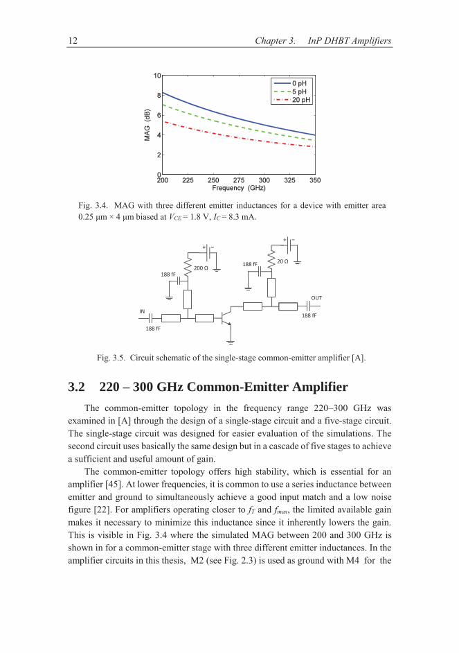
Fig. 3.4. MAG with three different emitter inductances for a device with emitter area 0.25 μm × 4 μm biased at VCE = 1.8 V, IC = 8.3 mA.
IN
OUT
200 Ω188 fF
20 Ω188 fF
188 fF
188 fF
Fig. 3.5. Circuit schematic of the single-stage common-emitter amplifier [A].
3.2 220 ‒ 300 GHz Common-Emitter Amplifier The common-emitter topology in the frequency range 220‒300 GHz was
examined in [A] through the design of a single-stage circuit and a five-stage circuit. The single-stage circuit was designed for easier evaluation of the simulations. The second circuit uses basically the same design but in a cascade of five stages to achieve a sufficient and useful amount of gain.
The common-emitter topology offers high stability, which is essential for an amplifier [45]. At lower frequencies, it is common to use a series inductance between emitter and ground to simultaneously achieve a good input match and a low noise figure [22]. For amplifiers operating closer to fT and fmax, the limited available gain makes it necessary to minimize this inductance since it inherently lowers the gain. This is visible in Fig. 3.4 where the simulated MAG between 200 and 300 GHz is shown in for a common-emitter stage with three different emitter inductances. In the amplifier circuits in this thesis, M2 (see Fig. 2.3) is used as ground with M4 for the

13
Fig. 3.6. Chip photograph of the single-stage common-emitter amplifier [A]. The circuit size is 0.39 mm × 0.45 mm.
Fig. 3.7. Chip photograph of the five-stage common-emitter amplifier [A]. The circuit size is 0.46 mm × 1.59 mm.
signal. This gives a short, and thereby low-inductive, connection from the emitter to ground. It also allows the M1 layer to be used for the dc wiring, as described in Section 4.1.
The two common-emitter amplifiers use transistors with emitter area 4 μm × 0.25 μm since simulations show that this device size gives the highest MAG in this frequency band. A circuit schematic of the single-stage circuit is shown in Fig. 3.5. The input and output matching networks are designed for maximum gain at the design frequency and both of them use a series transmission line with a short circuit stub. The base and collector bias are applied through the matching stubs with the RF shorted to ground through MIM capacitors. Series resistors provide stabilization from low frequency oscillations. Dc blocking at the input and output of the amplifier is provided by series MIM capacitors. The matching networks in the five-stage circuit are slightly adjusted from the single-stage design to optimize the gain and matching. Microphotographs of the single-stage amplifier and the five-stage amplifier are shown in Figs. 3.6 and 3.7, respectively. The total chip area is 0.39 mm × 0.45 mm for the single-stage circuit and 0.46 mm × 1.59 mm for the five-stage circuit.
The results from S-parameter measurements of the amplifiers are shown in Figs. 3.8(a) and 3.8(b). The five-stage amplifier has more than 10 dB gain from below

14 Chapter 3. InP DHBT Amplifiers
(a) (b)
Fig. 3.8. S-parameters of (a) the single-stage and (b) the five-stage common-emitter amplifier showing measured (solid lines), initial simulation (dotted lines) and adjusted simulation (dashed lines) [A].
Fig 3.9. Measured Y-factor for the five-stage common-emitter amplifier. Solid line indicates the median values [A].
Fig. 3.10. Measured (solid lines) and simulated (dashed lines) noise figure versus frequency for the five-stage common-emitter amplifier. The crosses show the median values, while the error bars indicate measured max and min values [A].

15
210 GHz up to 315 GHz with a peak gain of 24 dB at 250 GHz. The single-stage amplifier has a peak gain of 2 dB. The input and output return losses are below 0 dB over the entire bandwidth for both circuits. The devices were biased at VCE = 1.9 V, IC = 8.6 mA.
The measured S-parameters differ significantly from the simulated ones. There is a frequency shift of approximately 15% compared to the simulation results. The active device model from the foundry is extracted from measurements up to 50 GHz and no base inductance is included in the model, which explains part of the frequency shift [53]-[55]. Adjusting of the simulations by adding small series inductances, in the order of a few pH, on the base and the collector terminals of each device, resulted in better agreement between simulations and measurements.
The noise figure of the five-stage amplifier was measured with the Y-factor method described in Appendix A.3. For a lower noise figure, the DHBTs were biased slightly lower, VCE = 1.8 V, IC = 6.1 mA, than the bias point for maximum gain. The noise figure of the single-stage amplifier was not possible to measure due to the low gain. The Y-factor was very small also for the five-stage design and repeated measurement were made to achieve a statistically reliable result. The measured Y-factor at 240‒300 GHz is shown in Fig. 3.9. The solid line indicates the median value of the measurements at each frequency point. The noise figure could not be measured below 240 GHz due to limitations of the LO signal source. At 300 GHz the Y-factor was too small to distinguish.
The noise figure based on the median Y-factor is shown in Fig. 3.10 together with the simulated values. The measured noise figure is 10.4 dB at 265 GHz, which is the lowest reported noise figure above 200 GHz for amplifiers in bipolar technology.
3.3 250 ‒ 280 GHz Common-Base Amplifier It is visible in Fig. 3.1 that the common-base configuration offers higher gain
than the common-emitter cell above 100 GHz. A major drawback, however, is that the common-base configuration has poor stability and it is therefore necessary to stabilize the circuit [56]. Moreover, the stability and gain is very sensitive to base inductance [57]. Simulations show that the maximum gain decreases from 11.2 dB to 8.4 dB at 300 GHz, for a 4 μm × 0.25 μm device biased at VCE = 1.8 V and IC = 8.0 mA, with only 5 pH extra series inductance on the base. Another disadvantage is high output impedance, shown in Fig. 3.3, that makes it difficult to achieve an amplifier with good output matching.
A single-stage and a four-stage amplifier in common-base configuration were designed and fabricated in the InP DHBT process from Teledyne Scientific. The circuit schematic of the single-stage amplifier is shown in Fig. 3.11. The multistage

16 Chapter 3. InP DHBT Amplifiers
188 fF
120 fF
188 fF
120 fF
50 Ω
370 Ω
150 Ω
IN OUT
Fig. 3.11. Circuit schematic of the single-stage common-base amplifier [A].
Fig. 3.12. Microphotograph of the single-stage common-base amplifier [A]. The circuit size is 0.39 mm × 0.39 mm.
Fig. 3.13. Microphotograph of the four-stage common-base amplifier [A]. The circuit size is 0.87 mm × 0.46 mm.
circuit uses four cascaded stages similar to the single-stage circuit. The device is stabilized using a resistive feedback loop through a 370 Ω resistor between the collector and the emitter. The device is biased on the base through a series resistor with the RF short-circuited to ground through a MIM capacitor. This capacitor is placed close to the device to reduce the series inductance from base to ground. It is estimated from simulations in HFSS to 2.3 pH. The output matching network is similar to the common-emitter design with a matching stub that is shorted to ground

17
(a) (b)
Fig. 3.14. S-parameters of (a) the single-stage and (b) the four-stage common-base amplifier showing measured (solid lines), initial simulation (dotted lines) and adjusted simulation (dashed lines) [A].
through a MIM capacitor. The input matching network uses a short-circuited stub that provides dc ground. Chip photographs of the single-stage and four-stage amplifiers are shown in Figs. 3.12 and 3.13, respectively. The single-stage amplifier has a circuit area of 0.39 mm × 0.39 mm and the area of the four-stage amplifier is 0.46 mm × 0.87 mm.
The measured S-parameters of the single-stage amplifier and the four-stage amplifier are shown in Figs 3.14(a) and 3.14(b), respectively. The peak gain is 2.5 dB at 268 GHz for the single-stage circuit. The four-stage amplifier has a sharp gain peak at 268 GHz in combination with S11 and S22 close to, or above, 0 dB, which implies stability problems. The devices were biased low, VCE = 1.5 V, IC = 5 mA, in order to keep the circuit stable. The peak gain at this bias is 17 dB. The amplifier is narrowband with a gain above 10 dB between 265 and 285 GHz. The poor stability and the tilted gain are believed to be due to higher base inductance and more parasitic effects in the feedback loop than what was estimated initially.
3.4 80 ‒ 220 GHz Cascode Amplifier A two-stage cascode amplifier for operation in the frequency band 80 ‒ 220 GHz
was designed and characterized. The circuit schematic is shown in Fig. 3.15. The cascode cell in each stage is stabilized on the output with a shunt resistor, which is also utilized for providing collector current. The input matching network of each cascode cell consists of a short-circuited stub that is used for providing bias to the base of the common-emitter device. The output matching network utilizes an open stub. Base current to the common-base device is applied through a series resistor with the RF decoupled to ground through a capacitor. Series capacitors provide dc block on the amplifier input and output, and between the two stages. The active devices have an emitter area of 6 μm × 0.25 μm. A microphotograph of the circuit is shown in Fig. 3.16. The circuit size is 1.12 mm × 0.48 mm.

18 Chapter 3. InP DHBT Amplifiers
VC
RFin
VB1
VB2
VC
RFout
VB1
VB2190 fF
750 fF
3.3 pF 120 fF
100 Ω
20 Ω
190 fF
100 Ω
200 Ω
120 fF
100 Ω
20 Ω
750 fF
200 Ω
190 fF
3.3 pF 100 Ω
Fig. 3.15. Circuit schematic of the two-stage single-ended cascode amplifier.
Fig. 3.16. Microphotograph of the two-stage single-ended cascode amplifier. The circuit size is 1.12 mm × 0.48 mm.
Fig. 3.17. Measured (solid lines) and simulated (dashed lines) S-parameters of the two-stage single-ended cascode amplifier.
The measured and simulated S-parameters are shown in Fig. 3.17. The
measurements were carried out in three frequency bands: 10 MHz ‒ 110 GHz, 125 GHz ‒ 220 GHz, and 220 GHz ‒ 340 GHz. It was due to lack of measurement equipment not possible to measure between 110 and 125 GHz. The circuit was mounted on a resistive Si carrier to suppress substrate modes as described in Chapter 4. The upper end of the operational band is, as for the common-base amplifier, shifted down in frequency. The S-parameters show the benefits and drawbacks with the cascode configuration. The gain is high, considering that it is only two stages, and it is very wideband. The peak gain is approximately 20 dB

19
Fig. 3.18. Measured and simulated noise figure of the two-stage single-ended cascode amplifier.
between 110 and 145 GHz and more than 10 dB is available from 65 to 235 GHz. This amplifier is thus considerably more wideband than the common-emitter and common-base amplifiers presented in Sections 3.2 and 3.3. The output matching is however very poor due to the high output impedance of the cascode cell. The bias is low in the measurement, VCE = 2.0 V, IC = 7 mA (JE = 4.7 mA/μm2) for each device, in order to keep S22 below 0 dB, which causes the gain to decrease in the upper half of the frequency band. The input matching is better than 8 dB in the majority of the band.
The noise figure was measured from 155 to 205 GHz and the result is shown in Fig. 3.18. It follows the simulated values well and is below 10 dB up to 200 GHz with a minimum of 7.4 dB at 165 GHz. The devices were biased at the same bias point as in the S-parameter measurement.
3.5 Distributed Amplifiers The topology of a distributed amplifier (DA) differs considerably from the more
traditional amplifiers presented in Sections 3.3 and 3.4. The major benefit with this topology is the very wideband characteristics that such an amplifier can provide [28]. A DA consists of one input artificial transmission line (ATL) and one output ATL [22], [31]. The two ATLs are connected through one or several gain cells, e.g. a common-emitter stage or a cascode stage. A simple schematic of a DA with common-emitter cells is shown in Fig. 3.19. In this thesis, from here and onward, a DA with two or more gain cells as is shown in Fig. 3.19 will be termed conventional DA (CDA), whereas a DA with only one gain cell will be termed single-stage DA (SSDA).
The ATLs consist of series inductances and the input and output capacitances of each gain cell. As the input signal propagate along the input ATL it will be amplified and transferred to the output ATL. The portion of the signal that does not go into the

20 Chapter 3. InP DHBT Amplifiers
OUT
IN
Fig. 3.19. Simplified circuit schematic of a DA with common-emitter cells.
IN
rπ CπrbLi/2 Li
Cπrb Li
Cπrb
rπ rπ
Li/2
INreq Ceq
Li/2 Li Li Li/2
req Ceqreq Ceq
(a) (b)
Fig. 3.20. Small-signal models of input ATL of CDA with (a) device elements and with (b) equivalent parallel elements [B].
gain cells will be absorbed in the resistor that terminates the input ATL. If the phase difference between each gain cell is equal on both the input and output ATL, the amplified signal from each gain cell will add constructively in the forward direction [1]. In the backward direction the signals will cancel out most of each other and what remains will be absorbed in the terminating resistor. The preferred value of the series inductances depends on the input and output capacitances of the gain cells. The characteristic impedance of the ATLs is given by
(3.3)
where L is the series inductance and C the input, or output, capacitance [2]. For a well matched amplifier in a 50 Ω system L should be chosen such that Z0 = 50 Ω. The ATLs have a cut-off frequency that is approximated as
(3.4)
which limits the bandwidth for ideal lossless ATLs [22], [31]. In reality will both the bandwidth and the gain of a CDA be limited by resistive losses in the ATLs [31], [58]. The series inductive elements are, at frequencies above ~100 GHz, preferably realized as transmission lines with high characteristic impedance. Resistive losses in the transmission lines will add attenuation to the ATLs, but also the resistive input and output of the gain cells will contribute.

21
The input ATL for a CDA with either common-emitter or cascode stages in the gain cells can be modeled by the schematic in Fig. 3.20(a), where LI is the inductance of the transmission lines, rb the base resistance of the common-emitter device, rπ its input shunt resistance, and Cπ its input shunt capacitance. Resistive and conductive loss in the transmission lines are omitted. The device elements can be rearranged to parallel elements as shown in Fig. 3.20(b). The new elements are related to the original elements by
(3.5)
where ω is the angular frequency. It can be assumed that rb << rπ and (ωrbCπ)2 << 1. The values of the parallel elements can then be approximated by
(3.6)
and
(3.7)
Using the input ATL schematic in Fig. 3.20(b) the attenuation constant αI for one section of the ATL can be expressed as
(3.8)
Inserting the expressions from (3.6) and (3.7) the attenuation constant can be approximated by
(3.9)
It is consequently important to have a low base series resistance rb and a high input shunt resistance rπ for low attenuation in the input ATL. For the present process dominates the second term in (3.9) at frequencies above 100 GHz. A device with smaller device area has a lower input capacitance Cπ which reduces the input attenuation and thereby the bandwidth is increased. This comes however at the expense of lower gain and less output power [58].
The output resistance and capacitance differ significantly between a common-emitter cell and a cascode cell, as is visible in Fig. 3.3, since the cascode cell has a common-base stage on its output. The cascode cell has a very high output resistance and the output reactance is capacitive and dominated by the collector-to-base-capacitance, Cμ [49]. For the cascode |S22| is close to unity while S22 for the common-

22 Chapter 3. InP DHBT Amplifiers
OUT
V1
V1
1 kOhm
60 Ohm
50 Ohm10 Ohm
0.75 pF
0.75 pF
0.75 pF
V2IN
2 kOhmV1 1 kOhm
0.75 pF
2 kOhmV1 1 kOhm
0.75 pF
2 kOhm
Fig. 3.21. Circuit schematic of the conventional distributed amplifier [B].
Fig. 3.22. Microphotograph of the fabricated conventional distributed amplifier. The circuit size is 0.86 mm × 0.37 mm [B].
emitter cell approaches 50 Ω at higher frequencies. Consequently, the output ATL attenuation is much lower with cascode cells than with common-emitter cells. Apart from considerably better output impedance characteristic, the cascode cell has much higher gain than the common-emitter cell as is shown in Fig. 3.2. In CDAs, the cascode cell is therefore generally a better choice than the common-emitter cell.
3.5.1 Conventional Distributed Amplifiers A three-section CDA with cascode cells realized in the Teledyne InP DHBT
process were presented and demonstrated in [B]. The circuit schematic of the amplifier and a microphotograph of the fabricated chip are shown in Figs. 3.21 and 3.22, respectively. TFMLs are used for realizing the series inductances in the ATLs. The base bias to the common-emitter devices is applied through the terminating resistor of the input ATL. A decoupling capacitor short-circuit the RF signal to ground. The collector bias is applied in a similar manner using the output ATL. The base current supply to the common-base devices is provided by resistive voltage division utilizing the collector voltage source. The emitter area of the devices were chosen to 6 μm × 0.25 μm as this was regarded as a good compromise between bandwidth and gain. Simulations revealed that higher bandwidths appears to be

23
Fig. 3.23. Measured (solid lines) and simulated (dashed lines) S-parameters of the conventional distributed amplifier [B].
Fig. 3.24. Measured phase of S21, and measured (solid line) and simulated (dashed line) group delay variation of S21 versus frequency for the conventional distributed amplifier [B].
Fig. 3.25. Measured and simulated noise figure for the conventional distributed amplifier [B].
possible with smaller devices, but the average gain would decrease. Inductive peaking, using a series TFML, on the output of each gain cell increases the bandwidth and improves the gain flatness.

24 Chapter 3. InP DHBT Amplifiers
Fig. 3.26. Microphotograph of the second CDA that is designed for larger bandwidth. The circuit size is 0.56 mm × 0.96 mm.
Fig. 3.27. Measured (solid lines) and simulated (dashed lines) S-parameters of the CDA shown in Fig. 3.26.
The measured and simulated S-parameters are shown in Fig. 3.23. The amplifier was measured in two frequency bands: 70 kHz‒115 GHz and 130‒220 GHz. No measurement equipment were available between 115 and 130 GHz. The gain is higher than 10 dB from 70 kHz up to 180 GHz. Above 180 GHz, the gain drops sharply. The average gain between 20 GHz and 180 GHz is 13 dB with a gain variation of ±1.5 dB. Below 20 GHz, the gain increases and it has a peak at 5 GHz which is due to influence of dc probe inductance and limited capacitive decoupling. A linear phase characteristic of S21 is essential for transmission of digital signals [59], [60]. The phase of S21 and the derived group delay is shown in Fig. 3.24. The average group delay is close to 10 ps from 6 to 170 GHz, which is in good agreement with simulation. The noise figure of the CDA was measured in four frequency bands: 10 MHz‒26 GHz, 60‒105 GHz, 125‒160 GHz, and 165‒195 GHz. The result is shown in Fig. 3.25 together with simulated noise figure. The measured noise figure agrees well with the simulated one, except at the lowest frequencies where the gain is higher than

25
simulated. All the measurements were carried out with the circuit mounted on a resistive Si carrier.
In order to extend the bandwidth even further, a second CDA with smaller devices, 5 μm × 0.25 μm instead of 6 μm × 0.25 μm, was designed and characterized. A chip photograph of this CDA is shown in Fig. 3.26. The measured S-parameters are shown in Fig. 3.27. The upper frequency limit is extended by 40 GHz to 220 GHz. The measured average gain is 9.4 dB, with ±2.6 dB gain variation, between 10 and 223 GHz. The gain increases, as for the other CDA, dramatically below 10 GHz. Lower inductive peaking by reducing the transmission line lengths on the output of each cascode cell would possibly improve the stability and allowing higher bias and more gain. The high gain at low frequencies can most likely be reduced by more efficient capacitive decoupling in the bias network.
3.5.2 Cascaded Single-Stage Distributed Amplifier The CDA topology has fundamental limitations in gain. It is in (3.9) shown that
each sub sequential gain cell will increase the input ATL attenuation and the same is true for the output ATL. Each extra gain cell will receive less input power and on the output will the amplified signal from first gain cell that is propagating along the output ATL be attenuated more for each gain cell that is added. Ultimately, as the number of gain cells goes towards infinity, the gain will go towards zero [31], [61].
A DA topology that overcomes this limitation is the cascaded single-stage distributed amplifier (CSSDA). The CSSDA is based on a DA with only a single gain cell – a single-stage distributed amplifier (SSDA). Two or more SSDAs connected in cascade form a CSSDA. For a CSSDA, the gain grows exponentially to the number of gain cells and not to the square as for CDAs [62]. Previously, the CSSDA topology has only been demonstrated in HEMT and Si-based bipolar technologies at significantly lower frequencies [62]-[64].
Two circuits, an SSDA and a 2-cascaded SSDA (2-CSSDA), were designed and characterized to evaluate the CSSDA topology in InP DHBT technology at frequencies above 100 GHz and to compare it with the CDA topology. The circuit schematic of the SSDA is shown in Fig. 3.28(a). The amplifier is essentially one of the three sections in the CDA in Section 3.4.1. The base bias to the common-base device is separated from the collector bias in order to increase the tuning flexibility. The decoupling capacitors that terminates the input and output ATL are increased in size to improve the gain flatness at lower frequencies. A microphotograph of the fabricated circuit is shown in Fig. 3.28(b). The circuit size is 0.52 mm × 0.46 mm. The dc pads for Vb1 and VC is moved to the south side in order to simplify the dc circuitry and to have a shorter circuit.

26 Chapter 3. InP DHBT Amplifiers
OUT
Vb2
Vc
2 kOhm
60 Ohm
50 Ohm10 Ohm3 pF
3 pF
0.75 pF
Vb1IN
(a) (b)
Fig. 3.28. (a) Circuit schematic and (b) microphotograph of the SSDA. The circuit size is 0.52 mm × 0.46 mm [B].
Fig. 3.29. Measured (solid lines) and simulated (dashed lines) S-parameters of the SSDA [B].
Fig. 3.30. Measured and simulated noise figure for the SSDA [B].

27
IN
OUT
Vb2
Vc
2 kOhm
60 Ohm
50 Ohm10 Ohm
0.75 pF
0.75 pF
0.75 pF
Vb1
0.19 pF
0.75 pFVb2
Vc
2 kOhm
60 Ohm
50 Ohm10 Ohm
0.75 pF
0.75 pF
0.75 pF
Vb10.75 pF
Fig. 3.31. Circuit schematic of the 2-CSSDA [B].
Fig. 3.32. Microphotograph of the fabricated 2-CSSDA. The circuit size is 1.09 mm × 0.38 mm [B].
The circuit was measured in three frequency bands: 40 kHz ‒ 110 GHz,
140 ‒ 220 GHz, and 220 ‒ 325 GHz. The measured and simulated S-parameters are shown in Fig. 3.29. The gain is quite low, since it is only a single cascode stage, on average 7.5 dB with a gain variation of ±1 dB, but over a bandwidth from 1.3 GHz up to 194 GHz, which gives a fractional bandwidth of over 197 %. The bandwidth is however smaller than expected from the simulations. The noise figure, measured and simulated, is shown in Fig. 3.30. Due to the low gain of the circuit, the noise figure is difficult to measure which results in poor accuracy.
To achieve higher gain, a 2-CSSDA was designed. The circuit schematic of this amplifier is shown in Fig. 3.31. The output ATL of the first stage is connected to the input ATL of the second stage. The biasing of the circuit requires a dc block between the two stages. This is realized by a series MIM capacitor which inevitably results in a low frequency gain roll-off. The size of the decoupling capacitors could consequently be reduced compared to the SSDA since there is no gain at low frequencies. A microphotograph of the 2-CSSDA is shown in Fig. 3.32.

28 Chapter 3. InP DHBT Amplifiers
Fig. 3.33. Measured (solid lines) and simulated (dashed lines) S-parameters of the 2-CSSDA [B].
Fig. 3.34. Measured and simulated noise figure of the 2-CSSDA [B].
Fig. 3.35. Measured phase of S21, and measured (solid line) and simulated (dashed line) group delay variation of S21 versus frequency for the 2-CSSDA [B].
Fig. 3.33 shows the measured and simulated S-parameters for the 2-CSSDA. The
average gain is 16 dB with less than ±2 dB gain ripple over a bandwidth from 2.0 to 237 GHz. The measured noise figure, shown in Fig. 3.34, is less than 10 dB between 112 and 138 GHz, but it is higher than that expected from simulation below these

29
frequencies. The measured phase of S21 and the group delay are shown in Fig. 3.35. The average group delay is 14 ps between 10 and 280 GHz.
Table 3.1 shows a comparison of the DA circuits presented in this chapter and similar reported wideband amplifiers in various topologies. The SSDA and the 2-CSSDA are the most wideband amplifiers reported to date. The only circuit that is comparable to these two and the CDA is an amplifier [65] that uses the same DHBT process and a circuit topology that is very similar to that of the CDA presented in this thesis. These amplifiers clearly set a new standard of bandwidth for amplifiers.
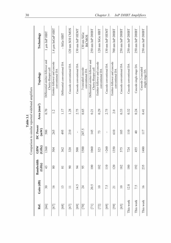
30 Chapter 3. InP DHBT Amplifiers
Tab
le 3
.1
Com
paris
on to
sim
ilar r
epor
ted
wid
eban
d am
plifi
ers
Tec
hnol
ogy
1 μm
InP
HB
T
1.4 μm
InG
aP H
BT
- SiG
e H
BT
120
nm S
OI C
MO
S
130
nm In
P H
EMT
130
nm S
iGe
BiC
MO
S 25
0 nm
InP
DH
BT
120
nm S
iGe
HB
T
130
nm In
P H
EMT
700
nm In
P D
HB
T
250
nm In
P D
HB
T
250
nm In
P D
HB
T
250
nm In
P D
HB
T
250
nm In
P D
HB
T
Top
olog
y
Diff
eren
tial e
mitt
er-fo
llow
er a
nd
Che
rry-H
oope
r cel
l Em
itter
-follo
wer
and
cas
code
co
nven
tiona
l DA
Diff
eren
tial c
onve
ntio
nal D
A
Cas
code
con
vent
iona
l DA
Cas
code
con
vent
iona
l DA
3-ca
scad
ed c
asco
de
conv
entio
nal D
A
Diff
eren
tial e
mitt
er-fo
llow
er a
nd
Che
rry-H
oope
r cel
l Em
itter
-follo
wer
and
cas
code
co
nven
tiona
l DA
Cas
code
con
vent
iona
l DA
Emitt
er-fo
llow
er a
nd c
asco
de
conv
entio
nal D
A
Cas
code
con
vent
iona
l DA
Cas
code
con
vent
iona
l DA
Cas
code
sing
le-s
tage
DA
Cas
code
2-c
asca
ded
sing
le-s
tage
DA
Are
a (m
m2 )
0.70
1.2
1.17
1.28
2.75
0.65
0.21
0.29
2.75
2.0
0.33
0.32
0.24
0.41
DC
Pow
er
(mW
) 50
0
265
495
210 -
247.
5
145
73
- 610
105
110
40
117
GB
W
(GH
z)
1360
504
362
320
500
1500
1060
323
>260
1350
575
724
455
1480
Ban
dwid
th
(GH
z)
43
80
81
90
94
95
100
102
110
120
182
180
192
235
Gai
n (d
B)
30
16
13
11
14.5
24
20.5
10
7.5 21
10
12.8
7.5 16
Ref
.
[66]
[67]
[68]
[67]
[69]
[70]
[71]
[72]
[69]
[59]
[65]
This
wor
k
This
wor
k
This
wor
k

31
Chapter 4
4 Suppression of Parasitic Substrate Modes
A fundamental concern in the design of microwave circuit elements is excitation of unwanted parasitic modes. Such modes might result in circuits that are unstable and not working properly. One type of parasitic modes that is problematic in circuits operating at high frequencies are modes that are propagating within the bulk substrate. In this chapter, the impact of such parasitic substrate modes on circuits with a multilayer back-end is discussed.
4.1 Substrate Modes and Resonances All the circuits described in Chapter 3 have a large ground layer, covering most
of the chip area, on the front-side of the circuit. This is a similarity they share with CPW circuits. If the circuit is placed on a conducting surface, i.e. metal, the ground layer and the surface will form two parallel conducting planes with high-ɛr substrate between them. Although the ground layer covers most of the circuit area, and thereby shields the substrate from the RF signal, there must be some openings in order to access the active devices, MIM capacitors, and resistors on the lower topographic levels. Through these ground plane openings, parasitic modes that propagate down into the substrate may be excited. The substrate behaves as a resonance box in which the substrate modes will bounce back and forth at certain frequencies that are given by
(4.1)
where l, w, and h are the length, width, and height of the bulk substrate and m, n, and p are the modal indices in the corresponding dimensions [1], [73]. The modal indices are equivalent to the number of half wavelengths in the respective direction. If fmnp is within the bandwidth of the circuit, the resonance may disturb its functionality.

32 Chapter 4. Suppression of Parasitic Substrate Modes
(a) (b) Fig. 4.1. (a) Simulation structure of a TFML passing over a ground plane opening. (b) S-parameters of the TFML with modal indices for the major resonances [C].
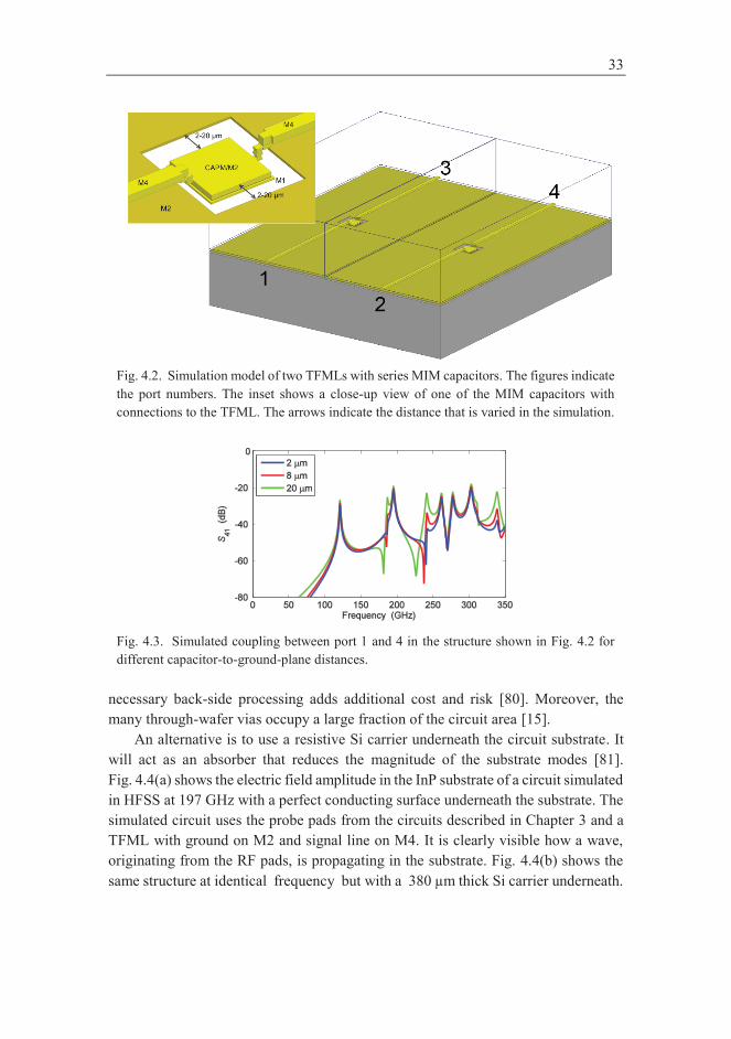
A simulation structure of a 50 Ω TFML thru-line passing over a ground plane
opening is shown in Fig. 4.1(a). The substrate is InP with dimensions 1.68 mm × 0.56 mm × 0.1 mm. The size of the ground plane opening is 50 μm × 75 μm, which is comparable to openings for e.g. a MIM capacitor in a real active circuit. The structure was simulated in HFSS and the resulting S-parameters are shown in Fig. 4.1(b). Several resonances are observed at frequencies that are in correspondence with (4.1). The modal indices of the major resonances are indicated in the figure.
The parasitic substrate modes can cause unwanted cross-talk between different parts of a circuit, which affect the circuit performance and stability [74]. A typical circuit element is a TFML with a series MIM capacitor. In the DHBT process from Teledyne Scientific, the MIM capacitor uses M1 and M2, as is shown in Fig. 2.3. There must consequently be an opening in the ground plane around the capacitor. A simulation structure of a 190 fF capacitor connected by stacked vias to microstrip lines on M4 is shown in Fig. 4.2. Two such structure are placed in parallel at a distance of 0.25 mm from each other. A vertical perfect conducting wall is placed above the ground plane in the middle between the two capacitors to prevent any cross-talk through the air. The simulated coupling between port 1 and 4 is shown in Fig. 4.2. The coupling is simulated for three different sizes of the ground plane opening – the separation distance between the capacitor and ground plane is changed as indicated in Fig. 4.2. Significant coupling, with S41 as high as -20 dB, is observed at distinct frequencies. The first peak is at the f110 resonance, which will, as the other resonances, shift to lower frequencies for an entire circuit with larger area and substrate volume. No major improvement is gained with smaller ground plane openings. The result shows that cross-talk between circuit elements far from each other may be a serious problem at the resonance frequencies.
A standard method to eliminate substrate modes is to add numerous through- wafer vias that are distributed over the entire circuit [15], [35], [73], [75]-[79]. The
33
Fig. 4.2. Simulation model of two TFMLs with series MIM capacitors. The figures indicate the port numbers. The inset shows a close-up view of one of the MIM capacitors with connections to the TFML. The arrows indicate the distance that is varied in the simulation.
Fig. 4.3. Simulated coupling between port 1 and 4 in the structure shown in Fig. 4.2 for different capacitor-to-ground-plane distances.
necessary back-side processing adds additional cost and risk [80]. Moreover, the many through-wafer vias occupy a large fraction of the circuit area [15].
An alternative is to use a resistive Si carrier underneath the circuit substrate. It will act as an absorber that reduces the magnitude of the substrate modes [81]. Fig. 4.4(a) shows the electric field amplitude in the InP substrate of a circuit simulated in HFSS at 197 GHz with a perfect conducting surface underneath the substrate. The simulated circuit uses the probe pads from the circuits described in Chapter 3 and a TFML with ground on M2 and signal line on M4. It is clearly visible how a wave, originating from the RF pads, is propagating in the substrate. Fig. 4.4(b) shows the same structure at identical frequency but with a 380 μm thick Si carrier underneath.

34 Chapter 4. Suppression of Parasitic Substrate Modes
(a) (b)
Fig. 4.4. Simulated electric field amplitude in the InP substrate with (a) a perfect conducting surface underneath the substrate and (b) a Si carrier with conductivity 10 S/m underneath the substrate [C].
The Si carrier is simulated with a conductivity of 10 S/m. There is still a wave propagating from the pads, but within a short distance, the amplitude of wave has been greatly reduced due to the Si carrier. Wafers of Si with conductivity 10‒100 S/m are industrial standard and offered at low cost. With this method to absorb substrate modes, the circuit processing is simpler since no back-side processing is necessary. In addition to this, the circuit area is used more efficient since no through-wafer vias are required. The drawback with a Si carrier is when the circuit generates significant heat, e.g. in a power amplifier, where the limited thermal conductivity of Si can introduce problems with heat removal.
4.2 Thin-Film Microstrip Thru-Line A test circuit was used in order to study the effects of substrate modes and to
verify the effectiveness of a Si carrier underneath the circuit. A microphotograph of the circuit is shown in Fig. 4.5. The substrate is InP with dimensions 1.68 mm × 0.56 mm × 100 μm. There are two metal layers, separated by 3 μm BCB, on the front-side. The back-side is not metalized. The circuit has a TFML thru-line that uses the first metal layer as ground and both ends of the TFML are terminated with GSG probe pads. The ground layer is uniform, and the substrate is thereby shielded from the RF, except at the ground slots of the GSG pads.
The thru-line circuit was mounted on three different materials: metal, Si, and Gel-Pak (type CD-22C-02-X0-P0037 [82]). The Si is a diced tile of a standard 380 μm thick wafer, n-doped to a conductivity of 10‒100 S/m. Gel-Pak is a carrier with plastic gel on top of a glass plate. It is frequently used for mounting of semiconductor circuits during test measurements and transport.
The S-parameters of the circuits were measured in two frequency bands: 140 ‒ 220 GHz and 220 ‒ 325 GHz. S21 and S11 of the three circuit configurations are shown in Figs. 4.6(a) and 4.6(b), respectively. Large variations, with several minima in S21, can be observed when the circuit is mounted on metal. The result indicates the presence of resonating substrate modes at numerous frequencies. The behavior is greatly improved with a Si carrier underneath the circuit. S21 is monotonically

35
Fig. 4.5. TFML thru-line test circuit on InP substrate with dimensions 1.68 mm × 0.56 mm × 100 μm [C].
(a) (b) Fig. 4.6. Measured (a) S21 and (b) S11 of the TFML thru-line test circuit mounted on metal, silicon, and Gel-Pak [C].
decreasing with frequency and there are no sharp variations in S11. The Si carrier effectively eliminates the influence of substrate modes on the thru-line. The circuit measured on Gel-Pak behaves well up to 240 GHz, but there are significant variations in the S-parameters above this frequency.
4.3 Substrate Modes in Active Circuits To examine the effects of substrate modes in active circuits, the five-stage
common-emitter amplifier presented in [A] and in Section 3.2 was used. Apart from the GSG pads, the circuit has several ground plane openings. The measurements in Fig. 3.8(b) are for a circuit with 300 μm thick InP substrate mounted on metal. Circuits from a second wafer with 100 μm thick substrate were mounted on metal and Si. The circuits were not diced individually, they were in the approximate center of a 6 mm × 6 mm large wafer tile shared with several other circuits.
The measured S-parameters for the three chips are shown in Fig. 4.7. The gain is more stable versus frequency for the chip with Si carrier compared to the chip with 300 μm thick substrate on metal in [A]. The higher overall gain is supposed to be a matter of process variations between the wafers rather than a cause of the thinner substrate and the Si carrier. The chip with 100 μm substrate on metal demonstrates

36 Chapter 4. Suppression of Parasitic Substrate Modes
Fig. 4.7. Measured S-parameters of the five-stage common-emitter amplifier presented in Section 3.2 with 100 μm thick substrate mounted on metal, 100 μm substrate mounted on Si carrier, and 300 μm substrate mounted on metal.
Fig. 4.8. Stability factor μ of the five-stage amplifier for the three different substrate configurations.
dramatic gain variations that are in the order of 3 dB. For the input, S11, and output matching, S22, the differences are even more significant. Both chips mounted on metal have large peaks in the middle of the frequency band whereas the chip on Si have well defined minima in both S11 and S22. The stability factor μ for each of the three circuits is shown in Fig. 4.8. For the chip mounted on Si carrier μ is larger than unity which shows that the circuit is unconditional stable, while both of the circuits mounted on metal have μ less than unity. The influence of parasitic substrate modes and the effectiveness of a resistive Si carrier are even more pronounced in the circuit shown in Fig. 4.9. This circuit is a five-stage common-emitter amplifier as well, but designed for lower frequencies. The

37
Fig. 4.9. Microphotograph of a second five-stage common-emitter amplifier. The circuit size is 1.80 mm × 0.72 mm [C].
Fig. 4.10. Measured S-parameters of the five-stage common-emitter amplifier shown in Fig. 4.9 with 100 μm thick substrate mounted on metal and 100 μm substrate mounted on Si carrier [C].
Fig. 4.11. Stability factor μ of the amplifier shown in Fig. 4.9 with 100 μm thick substrate mounted on metal and 100 μm substrate mounted on Si carrier [C].

38 Chapter 4. Suppression of Parasitic Substrate Modes
circuit is designed by Prof. H. Zirath, Microwave Electronics Lab., Chalmers Univ. of Tech. This amplifier was, in opposite to the first amplifier, measured individually diced. The measured S-parameters and the stability factor are shown in Figs. 4.10 and 4.11, respectively. The gain ripple is in the order of 10 dB and there are distinct peaks, greater than 0 dB, in both S11 and S22. With a Si carrier, the S-parameters are very flat versus frequency, e.g. the gain variation between 140 and 185 GHz is only ±0.75 dB. The reverse isolation, S12, is on average improved by 25 dB, which shows that unwanted feedback in the substrate is greatly reduced.
The measurements show that substrate modes may have a large impact on the functionality of circuits of this kind and that it is necessary to eliminate these modes. The use of a Si carrier is an effective method for this and it simplifies the circuit processing compared to substrate mode suppression with numerous through-wafer vias.

39
Chapter 5
5 Packaging and Waveguide Transitions
In the two previous chapters, integrated circuits with on-wafer measurements operating at frequencies up to 300 GHz were presented. Bare die circuits are however not useful outside the laboratory. In order to have a useful microwave component, e.g. an amplifier, it needs to be packaged in some kind of module with an interface that makes it possible to connect it to other components. At frequencies above 110 GHz, the dominating interface is the rectangular waveguide.
This chapter discusses different solutions for circuit-to-waveguide transitions. Amplifier modules with novel transitions, designed to accommodate circuits with multilayer back-end, such as the circuits presented in Chapter 3, are proposed. Modules for two frequency bands, WR05/G-band (140‒220 GHz) and WR03/H-band (220‒325 GHz), are demonstrated. These two modules demonstrate the first published results of InP DHBT amplifier modules operating at these high frequencies.
5.1 Waveguide Transitions A waveguide transition is necessary for coupling the fundamental TE10 mode
from the waveguide to a planar transmission line, e.g. a microstrip or a CPW. One of the most common transitions is what is usually referred to as E-plane probe [10], [83]-[87]. The E-plane probe is basically a planar transmission line that is extended into the waveguide through an opening in the broadwall of the waveguide. The surface of the E-plane probe is mounted in line with the waveguide propagation direction in the center of the broadwall where the electric field is strongest and with a distance to the waveguide back-short of approximately λ/4 [83]. A three-dimensional view is shown in Fig. 5.1.
To prevent unwanted modes from propagating through the opening in the broadwall, the cross-section area of this opening must be narrow [4], [83]. There are

40 Chapter 5. Packaging and Waveguide Transitions
Backshort
Propagation
Fig. 5.1. E-plane probe in rectangular waveguide with shortened end. The blue arrows indicate the electric field.
(a) (b)
(c)
Fig. 5.2. Different solutions on circuit-to-waveguide transitions: (a) E-plane transitions on separate substrates connected with bond wires. (b) Integrated E-plane transitions. (c) Integrated dipole transitions [D].
practical limits in scaling the width of the circuit and therefore either the probe must be placed on a separate transition substrate or the circuit substrate must have a non-rectangular shape with a smaller width near the transitions. Simplified drawings of these two solutions are shown in Figs. 5.2(a) and 5.2(b).
With a waveguide probe on a separate transition substrate, the circuit chip can be diced rectangular and the transition substrate can be a low permittivity material such as quartz (ɛr = 3.8), which reduces the losses [4]. The drawback is that a probe on a separate substrate needs a connection to the circuit. Bondwiring or ribbon-bonding is the most common alternative at lower frequencies. There is, however, practical limitations in scaling the bond wires and the effects of wire reactance become excessively high above 200 GHz [14], [88].
Integration of the probes on the circuit die simplifies the design and mounting [84]. The non-rectangular die size requires however complicated dicing tools, e.g. laser dicing process [84], [86], or die singulation through etching [76], [89].

41
Moreover, at frequencies above 200 GHz, the substrate must be thinned to 50 μm or less to reduce losses [35], [84], [87], [90].
An alternative to the E-plane probe that has been demonstrated successfully with several circuits is a planar dipole integrated on-chip, Fig. 5.2(c) [42], [75], [78]. This method has been utilized in amplifiers operating up to 670 GHz [76]. The loss for a single transition is typically 1 dB at 340‒380 GHz [78]. As for the integrated E-plane probe, the drawback is that the InP substrate must be very thin or the losses will be high. It is also necessary with through-substrate vias to suppress parasitic substrate modes. Integrated probes, both E-plane probes and dipoles, make it impossible to carry out probed on-wafer measurements of the circuit. To be able to test the circuit functionality prior to packaging it is necessary to design two versions, one with probe pads and one with integrated waveguide transitions [10], [15]. The abovementioned solutions require back-side metallization and through-wafer vias in order to connect the circuit ground with the waveguide block.
5.2 Transitions on Membrane Substrate To overcome the drawbacks with the transitions described in Section 5.1, a novel
circuit-to-waveguide transition using membrane technology was developed. Membrane technology is used successfully in waveguide modules that utilize Schottky diodes [91]-[94]. This is, however, to the author’s best knowledge, the first time this technology is used together with a transistor-based circuit. In membrane structures, the disadvantages with a dielectric support substrate at high mm-wave and submm-wave frequencies are overcome by using a very thin, <5 μm, membrane substrate [94].
Membrane transitions for two frequency bands, WR05 (140‒220 GHz) and WR03 (220‒325 GHz), were designed and manufactured. A CAD drawing of the WR03 membrane transition is shown in Fig. 5.3. The transition is mounted in an air channel between the waveguide and the circuit as is shown in Fig. 5.4(a). The substrate is 3 μm thick GaAs forming a thin membrane suspended in air within the channel. The transmission line is a CPW as shown in Fig. 5.4(b). The ground layers on each side extend 100 μm outside the GaAs substrate and are clamped between the two split-block halves. The clamped ground layer provide a well-defined ground as well as a mechanical support for the transition.
The GaAs substrate is removed at the end of the transition that is facing the circuit. Left is three beam leads for ground-signal-ground. The beam leads are 125 μm long and forms a CPW connection to the GSG pad on the circuit, as is shown in Fig. 5.4(a). The connection is very low reactive as opposed to a connection with bond wires. The two beam leads for ground provide a well-defined ground for the circuit. The beam leads are “glued” to the circuit pads by pressuring them with a

42 Chapter 5. Packaging and Waveguide Transitions
Fig. 5.3. Membrane transition for WR03.
(a) (b) Fig. 5.4. (a) Three-dimensional view of membrane waveguide transition and (b) cross-section view of its transmission line section with the signal line in the center. The arrows indicate the electric field [D].
wedge in a standard bonding machine. The probe pads on the circuit are fully compatible with GSG probes for on-wafer measurements. It is therefore, in opposite to circuits with integrated transitions, not necessary with two versions of the same circuit. GaAs was chosen due to the availability of an in-house Schottky process [94] using this material. Other materials with higher mechanical flexibility and lower loss, e.g. a polymer such as BCB, would probably be more suitable for this purpose.
5.3 Thru-Line Test Modules The first tests of the membrane transitions were conducted with the TFML thru-
line test circuit shown in Fig. 4.5 mounted in WR05 and WR03 modules. In order to allow machining of the module and mounting of the circuit with its waveguide transitions, the waveguide module is designed in two halves forming a split-block. The module is split along the centerline of the longer edge of the waveguide, i.e. in the E-plane. This gives the lowest loss since the currents of the dominant TE10 mode are not broken [95]. The split-blocks can be machined with very small tolerances – the precision is better than 2 μm. The blocks are fabricated in brass and are gold

43
Fig. 5.5. WR03 waveguide split-block.
(a) (b)
Fig. 5.6. Microphotograph of (a) WR05 and (b) WR03 membrane transitions mounted their respective waveguide modules [D].
(a) (b)
Fig. 5.7. Measured (solid lines) and simulated (dashed lines) S21 and S11 of (a) the WR05 and (b) the WR03 thru-line modules [D].
plated after machining. The modules are designed with the two waveguide ports collinear on opposite sides to allow easy connection to other waveguide components. The dimensions of the modules are 25 mm × 25 mm × 20 mm (w × l × h). A photograph of the WR03 split-block prior gold plating and mounting is shown in Fig. 5.5. The same blocks were used for both the thru-line test circuits and the amplifier circuits.

44 Chapter 5. Packaging and Waveguide Transitions
Fig. 5.8. Fabricated WR05 and WR03 amplifier modules [D].
Microphotographs of the mounted transitions with beam lead connections are
shown in Fig. 5.6. The top of the circuit is a few micrometers below the membrane and the beam leads are bent slightly downwards which causes the dark shadow. The test circuits were mounted on top of a resistive Si carrier in the split-block.
The measured S-parameters are shown in Fig. 5.7. The WR05 module was characterized using frequency extenders for both WR05 and WR03. No attempts were made to suppress the waveguide mismatch when using the WR03 extenders and therefore large ripples in insertion loss above 220 GHz, where these extenders were used, are present. The insertion loss is 3‒6 dB between 130 and 220 GHz. The return loss is better than 7 dB between 130 and 250 GHz. The WR03 module demonstrates a more flat response. The insertion loss is somewhat higher than expected from simulations: 6.8 dB at 220 GHz and it increases to 9.5 dB at 325 GHz. The return loss is better than 11.5 dB from 210 GHz to 340 GHz. The WR03 module covers thereby the entire WR03 waveguide band, which is defined as 220‒325 GHz [96].
5.4 140 ‒ 220 GHz and 220 ‒ 300 GHz Amplifier Modules
The five-stage common-emitter amplifier presented in [A] was used as demonstrator for the waveguide modules and the waveguide transitions. The WR05 and the WR03 amplifier modules are shown in Fig. 5.8. The split-blocks are identical to those used for the thru-line test circuits. A photograph of the circuit with transitions in the WR03 housing is shown in Fig. 5.9, where the Si carrier underneath the circuit is visible. The distance between the input and the output waveguides are 2.88 mm.
The S-parameters of the WR05 and WR03 amplifier modules are shown in Figs. 5.10 and 5.11, respectively, together with S-parameters from on-wafer measurements of the circuit. The WR05 module demonstrates 10 dB gain or more from 155 GHz to above 260 GHz. The loss from the packaging is approximately 2 dB when compared to on-wafer measurements at the same bias. The loss of a single

45
Fig. 5.9. Microphotograph of the five-stage InP DHBT common-emitter amplifier from [A] mounted together with membrane transitions and Si carrier in WR03 split-block housing [D].
Fig. 5.10. Measured S-parameters of the WR05 amplifier module (thick lines) and of the amplifier circuit measured on-wafer (thin lines) [D].
Fig. 5.11. Measured S-parameters of the WR03 amplifier module (thick lines) and of the amplifier circuit measured on-wafer (thin lines) [D].

46 Chapter 5. Packaging and Waveguide Transitions
(a) (b)
Fig. 5.12. Measured noise figure of (a) the WR05 and (b) the WR03 amplifier modules at room temperature [D].
Fig. 5.13. Measured noise temperature and gain of the WR03 amplifier module at room temperature, at 100 K, and noise temperature of amplifier circuit at 100 K compensated for losses in waveguide package [E].
membrane transition and one waveguide (12 mm long) is thus close to 1 dB. The WR03 module has a gain of 19 dB between 230 and 255 GHz and the gain is more than 10 dB from 210 to 290 GHz. The output matching, S22, is better than -10 dB over the entire measured frequency band. Whereas the input matching, S11, is below -10 dB from 225 to 330 GHz.
5.4.1 Noise Temperature Measurements The two amplifier modules were characterized in terms of noise at room
temperature and the WR03 module was also characterized at 100 K. The measured room temperature noise figures of the two modules for different collector currents are shown in Fig. 5.12. The minimum noise figure of the WR05 module is 9.7 dB at 195 GHz at IC = 35 mA. For the WR03 module is the noise figure relatively flat at 11 dB from 235 to 270 GHz.

47
TABLE 5.1 COMPARISON TO OTHER REPORTED AMPLIFIER MODULES >200 GHZ
Ref. Center freq. (GHz) Gain (dB) Noise Figure
(dB) Technology
[97] 210 17 9.4 100 nm GaAs mHEMT [77] 290 16 8.4 30 nm InP HEMT [84] 299 21.6 - 20 nm GaAs mHEMT [77] 300 17 8.4 30 nm InP HEMT [98] 325 25 8.7 35 nm InP HEMT [99] 330 10 8.7 35 nm InP HEMT
[100] 360 11 - <50 nm InP HEMT [15] 425 20 - 30 nm InP HEMT [98] 480 11.4 11.7 <50 nm InP HEMT [77] 550 10 - 30 nm InP HEMT [10] 600 14.1 15 20 nm GaAs mHEMT [14] 670 8 13 30 nm InP HEMT
This work, WR05
195 245
10 24
9.7 - 250 nm InP DHBT
This work, WR03 240 19 10.8 250 nm InP DHBT
The noise temperature of the WR03 module was measured cryogenically
between 235 and 265 GHz using the measurement setup described in Appendix A.3.1. The measured noise temperature and associated gain both at room temperature and at 100 K are shown in Fig. 5.13. The noise temperature at room temperature is between 3300 and 3800 K (10.8‒11.5 dB). At 100 K, the average noise temperature has decreased to 1800 K (8.5 dB). The noise performance is thus improved by a factor close to 2. Subtracting the amplifier module waveguide loss and the membrane transition loss, the average noise temperature of the amplifier circuit itself is estimated to 1100 K (6.8 dB), as shown in Fig. 5.13.
Table 5.1 shows a comparison with reported state-of-the-art amplifier modules operating above 200 GHz. Data for the WR05 amplifier module is shown for two frequencies since the noise figure was measured only up to 205 GHz. Amplifiers in InP HEMT technology dominates and have reached impressively high frequencies. Even though the InP DHBT technology suffers from poor noise characteristics, the noise figure s of the two DHBT modules are not very far from the HEMT modules at similar frequencies.


49
Chapter 6
6 Conclusions This thesis has focused on the design and characterization of InP DHBT
amplifiers operating up to submillimeter-wave frequencies. Amplifiers in the frequency range from 80 to 300 GHz with different transistor configurations have been presented and the potential of the InP DHBT technology for realizing extremely wideband amplifiers that can operate from the kHz range up to, and above, 200 GHz have been demonstrated. These amplifiers can for instance be used in future high speed wireless and fiber-optical communication links.
The high operational frequencies create a demand of new solutions on how to package the integrated circuits in modules with a suitable interface. The novel membrane transitions proposed in this thesis are, with their very wideband characteristics, a promising alternative to transitions integrated on the circuit die. The circuit die fabrication is simplified since several complicated processing steps are unnecessary with this method.
6.1 Future Work To truly take advantage of the InP DHBT technology, integration of the
amplifiers presented in this thesis with other circuit functionalities to realize a complete receiver or transceiver on a single circuit die is an obvious future work. The performance of the distributed amplifiers can be improved by including an emitter-follower before the cascode in each gain cell. This increase the input resistance and may thereby improve the overall bandwidth and gain. Simulations of a conventional distributed amplifier using such a gain cell has shown very promising results and this circuit currently under fabrication.
A different material in the support substrate of the membrane transitions could improve the electrical performance and the mechanical properties. An interesting direction for future work would be to scale it up in frequency – membrane technology with Schottky diodes has been demonstrated at frequencies above 1 THz.
Finally, the cryogenic measurements of the amplifier module at 100 K showed interesting results. However, it was due to shortage of time only possible with very

50 Chapter 6. Conclusions
few measurements. Further measurements at temperatures below 10 K and at different bias points would be of great interest. The measurement accuracy could most likely be improved with only minor changes in the measurement setup.

51
Chapter 7
Summary of the Appended Papers This chapter presents a brief summary of each of the appended papers together
with comments on my contributions. Although the first author has made the major part of the work, the contributions from the other authors have been of invaluable help and importance.
Paper A Design and Characterization of H-band (220‒325 GHz) Amplifiers in a 250 nm InP DHBT Technology K. Eriksson, V. Vassilev, and H. Zirath In this paper, the design and characterization of InP DHBT amplifiers in common-base and common-emitter topology are presented. The lowest noise figure above 200 GHz for a bipolar amplifier is demonstrated. I contributed with design, simulations and characterization of the amplifiers, and writing of the paper.
Paper B InP DHBT Distributed Amplifiers with up to 235 GHz Bandwidth K. Eriksson, I. Darwazeh, and H. Zirath In this paper, extremely wideband amplifiers are presented. Two of the amplifiers have the highest reported bandwidths for amplifiers regardless of transistor technology. I contributed with characterization, initial idea of the CSSDA topology, theoretical analysis, and most of the writing. The design work was carried out together with I. Darwazeh.

52 Chapter 7. Summary of the Appended Papers
Paper C Suppression of Parasitic Substrate Modes in Multilayer Integrated Circuits K. Eriksson, S. E. Gunnarsson, P.-Å. Nilsson, and H. Zirath In this paper, parasitic substrate modes in integrated circuits with multilayer back-end and TFML interconnects are studied and a simple method to suppress such modes is demonstrated. I contributed with initial idea of the study, simulations, measurements, and writing of the paper.
Paper D InP DHBT Amplifier Modules Operating Between 150 and 300 GHz Using Membrane Technology K. Eriksson, P. Sobis, S. E. Gunnarsson, J. Hanning, and H. Zirath In this paper, InP DHBT amplifier modules are presented. The modules use a novel waveguide-to-microstrip transition on membrane substrate. The paper reports the first measurement results of packaged InP DHBT amplifiers at these high frequencies. I contributed with initial idea of membrane transitions together with P. Sobis, design and simulations of membrane transitions and waveguide blocks, mechanical layout, assembly together with P. Sobis, measurements, and writing of the paper. The membrane transitions were fabricated by J. Hanning.
Paper E Cryogenic Noise Figure Measurement of InP DHBT Amplifier Module from 220 to 325 GHz K. Eriksson, N. Wadefalk, J. Schleeh, P. Sobis, J. Hanning, J. Kooi, and H. Zirath The first cryogenic noise temperature measurements of a circuit in InP DHBT technology are presented in this paper. A WR03 amplifier module (presented in [D]) is cooled to 100 K and its noise temperature is measured with the Y-factor method using a temperature controlled waveguide attenuator as hot and cold load. I contributed with initial idea and measurements together with N. Wadefalk at Low Noise Factory, and writing of the paper.

53
Acknowledgements First of all I would like to thank my main supervisor Herbert Zirath and my
examiner Jan Grahn for giving me the opportunity to pursue my work towards a Ph.D. and for their guidance in my research. I am very grateful to my co-supervisors Sten Gunnarsson, Vessen Vassilev, and Peter Sobis for all their invaluable help through many fruitful and encouraging discussions. Thanks also to Izzat Darwazeh at UCL for an excellent collaboration, it has been great to work with you. Niklas Wadefalk has been of great help and I thank him for his guidance and assistance in measurements and in amplifier design. I am especially thankful to Johanna Hanning for the many hours she has spent on processing membranes, which made it possible to realize the ideas on circuit packaging. Bertil Hansson, who tragically passed away one and half year before the finish of this thesis, was genuinely helpful during the circuit design work and in organizing the circuit tapeouts. I thank Carl-Magnus Kihlman for machining the waveguide modules and various fixtures that I have needed in the measurements setups. I also thank Jacob Kooi at Caltech for his assistance and feedback.
To all my colleagues at Microwave Electronics Laboratory, thank you for making it a really nice place to work at and for helping me during my Ph.D. studies. Thanks to Elin and my family for their support during this time.
Finally, I would like to acknowledge the financing institutions and collaboration
partners. This work has been supported by ‘Charmant’ (Strategic Research Center on Microwave Antenna Systems), ‘SoC lösningar för framtidens trådlösa applikationer’, and ‘High Speed Communications’ which are funded by the Swedish Foundation for Strategic Research (SSF). Part of the research was carried out in the GHz Centre in a joint research project financed by Swedish Governmental Agency of Innovation Systems (VINNOVA), Chalmers University of Technology, Omnisys Instruments, Low Noise Factory, Wasa Millimeter Wave, and SP Technical Research Institute of Sweden. Teledyne Scientific is acknowledged for processing the circuits. Low Noise Factory is acknowledged for providing access to their measurement lab and for assistance in the cryogenic measurements.


55
Appendix A
A High Frequency Measurements Characterization of circuits up to 300 GHz presents numerous challenges. Due
to the very large bandwidths of the circuits described in this thesis, it was at many occasions necessary to measure the circuits in several different frequency bands, since no measurement setup can measure frequencies from ~1 MHz up to 300 GHz. Techniques to measure S-parameters and noise figure are described in this chapter.
A.1 On-Wafer Probing Even though a waveguide interface often is used in the final system, it is
necessary with on-wafer measurements in the development and testing of circuits [101]. Standard in on-wafer measurements is to use RF probes with three pins arranged with the signal on the center pin and ground on the two outer pins, i.e. ground-signal-ground (GSG). The RF pads on the circuit have a CPW structure compatible with the GSG probe. In circuits with microstrip interconnects, the CPW mode is transferred to a microstrip mode next to the pads.
The same RF probe pad structure was used in all circuits in this thesis. The probe pads were designed to be compatible with not only probes with probe pin pitches from 50 to 100 μm, but also with the membrane transitions described in Chapter 5. To simplify mounting of the membrane beam leads, the center pad is 65 μm long, whereas the probe need a sliding distance of only 20 μm or less.
The positioning of the probe tips on the GSG pads is very crucial for the behavior of the probe-to-microstrip transition [b]. Fig. A.1(a) shows a three-dimensional schematic view of a CPW probe in contact with the GSG pads. If the probe tips are placed in the longitudinal middle of the pads, position B in Fig. A.2(b), the part of the central signal pad that is behind the probe tip will act as an open stub. If this length is a considerable fraction of the wavelength, the influence from that part of the pad will be significant. Fig. A.3 shows the measured S11 and S21 of the 700 μm long 50 Ω TFML in Fig. A.2(b). The probe tips were placed at the three different positions A, B, and C, that are indicated on the pads. The center pad is 32 μm × 65 μm and the

56 Appendix A. High Frequency Measurements
(a) (b) Fig. A.1. (a) Schematic view of coplanar probe on probe pads. (b) Microstrip thru-line, the dashed lines indicate the three different probe tip positions in the measurements.
(a) (b)
Fig. A.2. Measurements of (a) S11 and (b) S21 for the 700 μm long microstrip line in Fig. A.1(b) with the probe tips positioned at A, B, and C.
distance between each position is approximately 25 μm, which is equivalent to 20° at 300 GHz. The differences between the three measurements are significant: S11 changes from -13 dB at 300 GHz with the probe tips at position A, to -6.5 dB at position C. The results show the importance of correct probing in on-wafer measurements at these frequencies.
A.2 S-parameters Measurements Fundamental in the characterization of small-signal amplifiers are S-parameter
measurements. Systems for measuring S-parameters in the frequency bands 70 kHz‒110 GHz, 140‒220 GHz, and 220‒325 GHz have been used for characterizing the circuits in this thesis. The measurements can be extended outside these specified bands with some degradation in the accuracy.
The measurement systems need to be calibrated to the correct reference planes, i.e. contributions from cables, probes, etcetera must be de-embedded. There are different methods to calibrate the system which differs in the impedance standards

57
Fig. A.3. Probe station with network analyzer and frequency extenders.
that are measured and the assumptions of the standards that are made [102]. In the on-wafer measurements of the circuits in this thesis, the systems were calibrated using line-reflect-reflect-match (LRRM) with the reference planes at the probe tips. The utilized standards are a thru-line, open, short, and a 50 Ω load. A commercial calibration substrate (Cascade Microtech 138-356 [103]) were used. Thru-reflection-line (TRL) waveguide interface calibration was used for measurements of the waveguide modules described in Chapter 5.
A.3 Noise Figure Measurements The noise figure of a circuit is a measure of the degradation in the signal-to-noise
ratio as the signal passes through the circuit [50]. The noise performance of the circuits covered in this thesis was measured using the Y-factor method. An advantage with this method is that only relative power levels are measured and not absolute power levels [104]. Relative power levels can be measured with higher accuracy than absolute levels.
The Y-factor method uses the Rayleigh-Jeans approximation of the power radiated from a blackbody at temperature T:
(A.1)
where kB is the Bolzmann constant and B is the detection bandwidth [105]. In a Y-factor measurement, the noise figure is measured by terminating the circuit input with two different loads of known equivalent noise temperatures, one hot and one cold. The output power for each input termination is measured. From these two measurements is the Y-factor computed, where the Y-factor is defined as
(A.2)

58 Appendix A. High Frequency Measurements
LO Source
Spectrum Analyzer
ProbeProbe
Amplifier under test
SubharmonicMixer
THOT/TCOLD
IF Amplifiers
Antenna
(a) (b)
Fig. A.4. Setup (a) for noise measurements on-wafer with (b) detail photograph [A]. where Pout,HOT and Pout,COLD is the output power with hot and cold termination, respectively [106]. The Y-factor can, using (A.2), be rewritten as
(A.3)
where Treceiver is the equivalent noise temperature of the receiver, G is the gain of the receiver, THOT and TCOLD are the temperatures of the hot and cold input terminations, respectively. With THOT and TCOLD known, Treceiver can be derived as
(A.4)
Commercial solid-state noise sources are available at lower microwave frequencies, but for higher frequencies are usually absorbers at physical hot and cold temperatures utilized [92], [107]. The noise figures throughout this thesis are measured with absorbers (Eccosorb [108]) at room temperature and immersed in liquid nitrogen.
Accurate power measurements at frequencies close to the submillimeter-wave range are difficult and mixing to IF is necessary [105], [109]. A measurement setup for on-wafer characterization of an amplifier is shown in Fig. A.4. The receiver consists of, counted from the input: horn antenna, input probe, the amplifier under test, output probe, harmonic mixer with LO chain, and IF amplifiers. The output power is measured with a spectrum analyzer.
To find the noise temperature of the amplifier, the other parts of the receiver that contributes to Treceiver must be subtracted. The receiver can be regarded as a system of cascaded components, where each component adds noise as

59
, (A.5)
where TPROBEin and TPROBEout are the noise temperatures of the input and output probes, respectively, Tamplifier is the noise temperature of the amplifier, Tmixer/IF is the noise temperature of the mixer and IF-chain, Gamplifier is the gain of the amplifier, GPROBEin and GPROBEout are the gain of the input and output probes, respectively [50]. Since the probes are passive, their noise temperatures depend only on their loss and their physical temperature. The receiver temperature in (A.5) can thus be rewritten as
, (A.6)
where LPROBEin and LPROBEout are the losses of the input and output probe, respectively, and TRT the room temperature (293 K). The noise temperature of the amplifier can then be expressed as
. (A.7)
To find Tmixer/IF, a second Y-factor measurement with the mixer input terminated with the hot and cold loads is carried out. In this calibration measurement, the noise temperature Tmixer/IF can be calculated directly from (A.4). The noise figure is finally derived from the noise temperature as
(A.8)
where T0 = 290 K [51]. The noise temperature is a more appropriate figure-of-merit at cryogenic temperatures since the noise figure is related to the standard room temperature T0 = 290 K. By sweeping the LO frequency to the mixer, the noise temperature of the amplifier under test can be measured versus frequency.
A.3.1 Cryogenic Noise Temperature Measurements Measurements at cryogenic temperatures is challenging since they are carried out
inside an enclosed chamber. It is necessary to have vacuum in the chamber in order

60 Appendix A. High Frequency Measurements
LO Source
Amplifier under test
SubharmonicMixer
IF Amplifiers
Steel WaveguideWR10 to
WR03 taper
Temperature- Controlled Attenuator
Power Meter
DEWAR
Fig. A.5. Measurement setup for cryogenic noise temperature measurements of amplifier waveguide module at 235‒265 GHz [E].
Attenuator Taper Mixer
Amplifierunder test Steel waveguide
IF
Fig. A.6. Photograph of the cryogenic measurement setup inside the dewar.
to have thermal isolation and to avoid condensation and freezing of water. A waveguide connection into the chamber must therefore have a transition that prevents air from entering the chamber through the waveguide. A main problem with Y-factor measurements at cryogenic temperatures and at frequencies above ~100 GHz is the realization of hot/cold temperature loads. The use of absorbing materials, e.g. Eccosorb, as described above for room temperature measurements, requires either bulky chopper wheels and collimating mirrors inside the chamber [110] or a window in the chamber wall that allows the absorber to be placed outside the chamber [111], [112].
Fig. A.5 shows a schematic of the cryogenic noise measurement setup used in [E] to measure the WR03 amplifier module presented in Section 5.4. A photograph of the part of the setup inside the chamber is shown in Fig. A.6. As hot/cold load is a temperature controlled WR10 attenuator used. The attenuator is developed by Jacob Kooi at the Submillimeter Astronomy and Instrumentation Group, California Institute of Technology, for measurements of W-band amplifiers. The vane inside the attenuator is thermally isolated and is heated by a resistor. The temperature is

61
measured with a sensor mounted on the vane. The second port of the attenuator is terminated with a short. TCOLD will thus be the ambient temperature inside the cryogenic chamber and THOT the temperature when the vane is heated.
The WR10 attenuator is connected to the amplifier module under test via a WR10-to-WR03 taper. A WR03 sub-harmonic mixer is mounted inside the chamber to avoid excessive RF loss. The LO signal is provided by a signal generator and WR06 ×4 multiplier chain located outside the chamber. A mylar film is used to attain an airtight connection into the chamber. To reduce thermal loss is a 4 inch long WR06 waveguide in stainless steel utilized. The IF signal from the mixer is connected with a coaxial cable to an IF amplifier chain and a power meter outside the cryogenic chamber. All the components inside the chamber are thermally connected to the cold head of the closed-cycle refrigerator. The measurement system is fully automatized with the LO frequency stepped and the output power and input load temperature measured at each frequency step.


63
References [1] D. M. Pozar, Microwave Engineering. Hoboken, NJ., USA: John Wiley &
Sons, Inc., 2005.
[2] R. E. Collin, Foundations for Microwave Engineering. Hoboken, NJ., USA: John Wiley & Sons, Inc., 2001.
[3] M. Rodwell, "100+ GHz transistor electronics; present and projected capabilities," in IEEE Topical Meeting Microw. Photonics, 2010, pp. 412-413, 2010.
[4] L. A. Samoska, "An Overview of Solid-State Integrated Circuit Amplifiers in the Submillimeter-Wave and THz Regime," IEEE Trans. THz Sci. Technol., vol. 1, pp. 9-24, 2011.
[5] DARPA Circuit Achieves Speeds of 1 Trillion Cycles per Second, Earns Guinness World Record. Available: http://www.darpa.mil/newsevents/releases/2014/10/28.aspx
[6] G. Raghavan, M. Sokolich, and W. E. Stanchina, "Indium phosphide ICs unleash the high-frequency spectrum," IEEE Spectrum, vol. 37, pp. 47-52, 2000.
[7] T. Mimura, S. Hiyamizu, T. Fujii, and K. Nanbu, " A New Field-Effect Transistor with Selectively Doped GaAs/n-AlxGa1-xAs Heterojunctions," Jpn. J. Appl. Phys., vol. 19, pp. L225-L227, 1980.
[8] F. Schwierz and J. J. Liou, Modern Microwave Transistors - Theory, Design, and Performance. Hoboken, NJ., USA: John Wiley & Sons, Inc., 2003.
[9] J. J. Komiak, P. M. Smith, K. H. G. Duh, D. Xu, and P. C. Chao, "Metamorphic HEMT Technology for Microwave, Millimeter-Wave, and Submillimeter-Wave Applications," in IEEE Compound Semicond. IC Symp., pp. 1-4, 2013.

64 References
[10] A. Tessmann, A. Leuther, H. Massler, V. Hurm, M. Kuri, M. Zink, M. Riessle, H. P. Stulz, M. Schlechtweg, O. Ambacher, "A 600 GHz low-noise amplifier module," in IEEE MTT-S Int. Microw. Symp. Dig., pp. 1-3, 2014.
[11] B. A. Orner, M. Dahlström, A. Pothiawala, R. M. Rassel, Q. Liu, H. Ding, M. Khater, D. Ahlgren, A. Joseph, and J. Dunn, "A BiCMOS Technology Featuring a 300/330 GHz (fT/fmax) SiGe HBT for Millimeter Wave Applications," in Bipolar/BiCMOS Circuits Tech. Meeting, pp. 1-4, 2006.
[12] U. R. Pfeiffer, E. Ojefors, A. Lisauskas, and H. G. Roskos, "Opportunities for silicon at mmWave and Terahertz frequencies," in Bipolar/BiCMOS Circuits Tech. Meeting, 2008, pp. 149-156, 2008.
[13] M. J. W. Rodwell, M. Urteaga, T. Mathew, D. Scott, D. Mensa, Q. Lee, J. Guthrie, Y. Betser, S. C. Martin, R. P. Smith, S. Jaganathan, S. Krishnan, S. I. Long, R. Pullela, B. Agarwal, U. Bhattacharya, L. Samoska, and M. Dahlström, "Submicron scaling of HBTs," IEEE Trans. Electron Devices, vol. 48, pp. 2606-2624, 2001.
[14] W. Deal, X. B. Mei, K. M. K. H. Leong, V. Radisic, S. Sarkozy, and R. Lai, "THz Monolithic Integrated Circuits Using InP High Electron Mobility Transistors," IEEE Trans. THz Sci. Technol., vol. 1, pp. 25-32, 2011.
[15] W. R. Deal, K. Leong, A. Zamora, V. Radisic, and X. B. Mei, "Recent progress in scaling InP HEMT TMIC technology to 850 GHz," in IEEE MTT-S Int. Microw. Symp. Dig., pp. 1-3, 2014.
[16] J. Hacker, M. Urteaga, R. Lin, A. Skalare, I. Mehdi, J. S. Rieh, and M. Kim, "400 GHz HBT Differential Amplifier Using Unbalanced Feed Networks," IEEE Microw. Wireless Compon. Lett., vol. 22, pp. 536-538, 2012.
[17] J. Hacker, M. Urteaga, S. Munkyo, A. Skalare, and R. Lin, "InP HBT amplifier MMICs operating to 0.67 THz," in IEEE MTT-S Int. Microw. Symp. Dig., pp. 1-3, 2013.
[18] M. Seo, M. Urteaga, A. Young, J. Hacker, A. Skalare, R. Lin, M. Rodwell, "A single-chip 630 GHz transmitter with 210 GHz sub-harmonic PLL local oscillator in 130 nm InP HBT," in IEEE MTT-S Int. Microw. Symp. Dig., pp. 1-3, 2012.
[19] J. Hacker, S. Munkyo, A. Young, Z. Griffith, M. Urteaga, T. Reed, and M. Rodwell, "THz MMICs based on InP HBT Technology," in IEEE MTT-S Int. Microw. Symp. Dig. , pp. 1126-1129, 2010.

65
[20] M. Urteaga, R. Pierson, P. Rowell, M. Choe, D. Mensa, and B. Brar, "Advanced InP DHBT process for high speed LSI circuits," in Proc. IEEE InP Re. Mater. Conf., pp. 1-5, 2008.
[21] M. Abbasi, S. E. Gunnarsson, N. Wadefalk, R. Kozhuharov, J. Svedin, S. Cherednichenko, I. Angelov, I. Kallfass, P. Leuther, and H. Zirath, "Single-Chip 220-GHz Active Heterodyne Receiver and Transmitter MMICs With On-Chip Integrated Antenna," IEEE Microw. Theory. Techn., vol. 59, pp. 466-478, 2011.
[22] S. Voinigescu, High-Frequency Integrated Circuits. New York, USA: Cambridge University Press, 2013.
[23] H. J. Song, K. Ajito, A. Hirata, A. Wakatsuki, Y. Muramoto, T. Furuta, N. Kukutsu, T. Nagatsuma, and Y. Kado, "8 Gbit/s wireless data transmission at 250 GHz," Electron. Lett., vol. 45, pp. 1121-1122, 2009.
[24] I. Kallfass, J. Antes, T. Schneider, F. Kurz, D. Lopez-Diaz, S. Diebold, H. Massler, A. Leuther, and A. Tessmann, "All Active MMIC-Based Wireless Communication at 220 GHz," IEEE Trans. THz Sci. Technol., vol. 1, pp. 477-487, 2011.
[25] Y. Yu, Y. B. Karandikar, S. E. Gunnarsson, M. Urteaga, R. Pierson, and H. Zirath, "340 GHz Integrated Receiver in 250 nm InP DHBT Technology," IEEE Trans. THz. Sci. Technol., vol. 2, pp. 306-314, 2012.
[26] V. Radisic, D. W. Scott, A. Cavus, and C. Monier, "220-GHz High-Efficiency InP HBT Power Amplifiers," IEEE Trans. Microw Theory Techn., vol. 62, pp. 3001-3005, 2014.
[27] A. Iqbal and I. Z. Darwazeh, "A 23 GHz Baseband HBT Distributed Amplifier for Optical Communication Systems," in Eur. Microw. Conf., pp. 6-11, 1998.
[28] T. Swahn, Y. Baeyens, and M. Meghelli, "ICs for 100-Gb/s serial operation," IEEE Microw. Mag., vol. 10, pp. 58-67, 2009.
[29] V. Radisic, M. Yu, L. Zhihao, V. Ho, X. Muliang, K. Guinn, S. Lee, and K. C. Wang, "40 Gb/s differential traveling wave modulator driver," IEEE Microw. Wireless Comp. Lett., vol. 13, pp. 332-334, 2003.
[30] H. Shigematsu, M. Sato, T. Hirose, and Y. Watanabe, "A 54-GHz distributed amplifier with 6-Vpp output for a 40-Gb/s LiNbO3 modulator driver," IEEE J. Solid-State Circ., vol. 37, pp. 1100-1105, 2002.
66 References
[31] B. Agarwal, A. E. Schmitz, J. J. Brown, M. Matloubian, M. G. Case, M. Le, M. Lui, and M. Rodwell., "112-GHz, 157-GHz, and 180-GHz InP HEMT traveling-wave amplifiers," IEEE Trans. Microw. Theory Techn., vol. 46, pp. 2553-2559, 1998.
[32] Teledyne Scientific (2015). Available: http://www.teledyne-si.com/
[33] M. Dahlström, "Ultra High Speed InP Heterojunction Bipolar Transistors," Ph.D. thesis, Department of Microelectronics and Information Technology, Royal Institute of Technology, Stockholm, 2003.
[34] Teledyne Scientific, "TSC250v1.0 Design Manual."
[35] M. Seo, M. Urteaga, J. Hacker, A. Young, Z. Griffith, V. Jain, R. Pierson, P. Rowell, A: Skalare, A: Peralta, R. Lin, D. Pukala, and M. Rodwell, "InP HBT IC Technology for Terahertz Frequencies: Fundamental Oscillators Up to 0.57 THz," IEEE J. Solid State Circuits, vol. 46, pp. 2203-2214, 2011.
[36] M. J. W. Rodwell, M. Le, and B. Brar, "InP Bipolar ICs: Scaling Roadmaps, Frequency Limits, Manufacturable Technologies," Proceedings of the IEEE, vol. 96, pp. 271-286, 2008.
[37] T. Merkle, A. Leuther, S. Koch, I. Kallfass, A. Tessmann, S. Wagner, H. Massler, M. Schlechtweg, and O. Ambacher, "Backside Process Free Broadband Amplifier MMICs at D-Band and H-Band in 20 nm mHEMT Technology," in IEEE Compound Semicond. IC Symp., 2014, pp. 1-4, 2014.
[38] M. Schlechtweg, A. Bessemoulin, A. Tessmann, S. Kudszus, W. Marsetz, W. H. Haydl, and A. Hulsmann, "Trends and Challenges in Coplanar Millimeter-Wave Integrated Circuit Design," in 30th Eur. Microw. Conf., 2000, pp. 1-4, 2000.
[39] A. Tessmann, A. Leuther, H. Massler, M. Kuri, and R. Loesch, "A Metamorphic 220-320 GHz HEMT Amplifier MMIC," in IEEE Compound Semicond. IC Symp., pp. 1-4, 2008.
[40] W. R. Deal, X. B. Mei, V. Radisic, W. Yoshida, P. H. Liu, J. Uyeda, M. Barsky, T. Gaier, A. Fung, and R. Lai, "Demonstration of a S-MMIC LNA with 16-dB Gain at 340-GHz," in IEEE Compound Semicond. IC Symp., pp. 1-4, 2007.

67
[41] X. B. Mei, W. Yoshida, W. R. Deal, P. H. Liu, J. Lee, J. Uyeda, L. Dang, J. Wang, W. Liu, D. Li, M. Barsky, Y. M. Kim, M. Lange, T. P. Chin, V. Radisic, T. Gaier, A. Fung, L. Samoska, and R. Lai, "35-nm InP HEMT SMMIC Amplifier With 4.4-dB Gain at 308 GHz," IEEE Electron Device Lett. , vol. 28, pp. 470-472, 2007.
[42] V. Radisic, K. M. K. H. Leong, X. Mei, S. Sarkozy, W. Yoshida, and W. R. Deal, "Power Amplification at 0.65 THz Using InP HEMTs," IEEE Trans. Microw. Theory Techn., vol. 60, pp. 724-729, 2012.
[43] Keysight Technologies - Advanced Desgin System (ADS). Available: http://www.keysight.com/en/pc-1297113/advanced-design-system-ads?cc=SE&lc=eng
[44] J. B. Hacker, Y. M. Lee, H. J. Park, J. S. Rieh, and M. Kim, "A 325 GHz InP HBT Differential-Mode Amplifier," IEEE Microw. Wireless Compon. Lett., vol. 21, pp. 264-266, 2011.
[45] V. Radisic, D. Scott, W. Sujane, A. Cavus, A. Gutierrez-Aitken, and W. R. Deal, "235 GHz Amplifier Using 150 nm InP HBT High Power Density Transistor," IEEE Microw. Wireless Compon. Lett., vol. 21, pp. 335-337, 2011.
[46] H. J. Park, J. S. Rieh, M. Kim, and J. B. Hacker, "300 GHz six-stage differential-mode amplifier," in IEEE MTT-S Int. Microw. Symp. Dig., pp. 49-52, 2010.
[47] A. R. Hambley, Electronics. Upper Saddle River, NJ, USA: Prentice Hall, Inc., 2000.
[48] T. K. Johansen and Y. Lei, "Design of mm-wave InP DHBT power amplifiers," in SBMO/IEEE MTT-S Int. Microw. Optoelectr. Conf., pp. 357-360, 2011.
[49] P. R. Gray, P. J. Hurst, S. H. Lewis, R. G. Meyer, Analysis and Design of Analog Integrated Circuits. Hoboken, NJ, USA: John Wiley & Sons, 2010.
[50] G. Gonzalez, Microwave Transistor Amplifiers - Analysis and Design. Upper Saddle River, NJ, USA: Prentice-Hall, Inc, 1997.
[51] D. M. Pozar, Microwave and RF Design of Wireless Systems. New York, USA: John Wiley & Sons, Inc., 2001.

68 References
[52] Ansys HFSS. Available: www.ansys.com
[53] M. Urteaga, M. Seo, J. Hacker, Z. Griffith, A. Young, R. Pierson, P. Rowell, A. Skalare, V. Jain, E. Lobisser, and M. Rodwell, "InP HBTs for THz frequency integrated circuits," in Proc. IEEE InP Rel. Mater. Conf., pp. 1-4, 2011.
[54] M. Urteaga, Teledyne Scientific Company, Thousand Oaks, USA, private communication, May 2013.
[55] V. K. Paidi, Z. Griffith, W. Yun, M. Dahlstrom, M. Urteaga, N. Parthasarathy, M. Seo, L. Samoska, A. Fung, and M. Rodwell, "G-band (140-220 GHz) and W-band (75-110 GHz) InP DHBT medium power amplifiers," IEEE Trans. Microw. Theory Techn., vol. 53, pp. 598-605, 2005.
[56] M. Seo, M. Urteaga, J. Hacker, A. Young, A. Skalare, R. Lin, and M. Rodwell, "A 600 GHz InP HBT amplifier using cross-coupled feedback stabilization and dual-Differential Power Combining," in IEEE MTT-S Int. Microw. Symp. Dig., pp. 1-3, 2013.
[57] T. B. Reed, Z. Griffith, P. Rowell, M. Field, and M. Rodwell, "A 180mW InP HBT Power Amplifier MMIC at 214 GHz," in IEEE Compound Semicond. IC Symp., pp. 1-4, 2013.
[58] K. W. Kobayashi, R. Esfandiari, and A. K. Oki, "A novel HBT distributed amplifier design topology based on attenuation compensation techniques," in IEEE MTT-S Int. Microw. Symp. Dig., pp. 447-450 vol.1, 1994.
[59] V. Hurm, F. Benkhelifa, R. Driad, R. Losch, R. Makon, H. Massler, J. Rosenzweig, M. Schlechtweg, and H. Walcher, "InP DHBT-based distributed amplifier for 100 Gbit/s modulator driver operation," Electron. Lett., vol. 44, pp. 705-706, 2008.
[60] E. Cohen, Y. Betser, B. Sheinman, S. Cohen, V. Sidorov, A. Gavrilov, and D. Ritter, "75 GHz InP HBT distributed amplifier with record figures of merit and low power dissipation for OEIC applications," in Proc. IEEE InP Re. Mater. Conf., pp. 609-612, 2005.
[61] Y. Ayasli, R. L. Mozzi, J. L. Vorhaus, L. D. Reynolds, and R. A. Pucel, "A Monolithic GaAs 1-13-GHz Traveling-Wave Amplifier," IEEE Trans. Microw. Theory Techn., vol. 30, pp. 976-981, 1982.

69
[62] B. Y. Banyamin and M. Berwick, "Analysis of the performance of four-cascaded single-stage distributed amplifiers," IEEE Trans. Microw. Theory Techn., vol. 48, pp. 2657-2663, 2000.
[63] L. Kai-Yun, I. S. Chen, and C. Hwann-Kaeo, "A 26- 65 GHz GaAs pHEMT cascaded single stage distributed amplifier with high gain/area efficiency," in IEEE Asia-Pacific Microw. Conf., pp. 722-725, 2006.
[64] K. L. Koon, Z. Hu, H. Aghvami, and A. A. Rezazadeh, "High gain and ultra wideband SiGe/BiCMOS cascaded single stage distributed amplifier for 4G RF front-end applications," in IEEE Proc. Personal, Indoor Mobile Radio Com., pp. 2180-2184 vol.3, 2003.
[65] Y. Sangwoo, I. Lee, M. Urteaga, M. Kim, and J. Sanggeun, "A Fully-Integrated 40-222 GHz InP HBT Distributed Amplifier," IEEE Microw. Wireless Compon. Lett., vol. 24, pp. 460-462, 2014.
[66] L. Zhihao, K. Guinn, J. Jensen, S. Thomas, C. Fields, and M. Sokolich, "A DC-43GHz-Bandwidth 30dB-Gain Amplifier," in IEEE MTT-S Int. Microw. Symp. Dig., pp. 1664-1667, 2006.
[67] J. Kim, J. O. Plouchart, N. Zamdmer, R. Trzcenski, R. Groves, M. Sherony, Y. Tan, M. Talbi, J. Safran, and L. Wagner, "A 12dBm 320GHz GBW distributed amplifier in a 0.12 μm SOI CMOS," in IEEE Int. Solid-State Circuits Conf. Dig., pp. 478-540 Vol.1, 2004.
[68] O. Wohlgemuth, P. Paschke, and Y. Baeyens, "SiGe broadband amplifiers with up to 80 GHz bandwidth for optical applications at 43 Gbit/s and beyond," in Eur. Microw. Conf., pp. 1087-1090 Vol.3, 2003.
[69] S. Masuda, T. Takahashi, and K. Joshin, "An over-110-GHz InP HEMT flip-chip distributed baseband amplifier with inverted microstrip line structure for optical transmission system," IEEE J. Solid-State Circuits, vol. 38, pp. 1479-1484, 2003.
[70] A. Arbabian and A. M. Niknejad, "A three-stage cascaded distributed amplifier with GBW exceeding 1.5THz," in IEEE Radio Freq. IC Symp., pp. 211-214, 2012.
[71] S. Daneshgar, Z. Griffith, and M. J. W. Rodwell, "A DC-100 GHz Bandwidth and 20.5 dB Gain Limiting Amplifier in 0.25 μm InP DHBT Technology," in Proc. IEEE Compound Semicond. IC Symp., pp. 1-4, 2013.

70 References
[72] J. Kim and J. F. Buckwalter, "A DC-102GHz broadband amplifier in 0.12μm SiGe BiCMOS," in IEEE Radio Freq. IC Symp., pp. 53-56, 2009.
[73] W. H. Haydl, "On the use of vias in conductor-backed coplanar circuits," IEEE Trans. Microw. Theory Techn., vol. 50, pp. 1571-1577, 2002.
[74] A. Tessmann, W. H. Haydl, T. V. Kerssenbrock, P. Heide, and S. Kudszus, "Suppression of parasitic substrate modes in flip-chip packaged coplanar W-band amplifier MMICs," in IEEE MTT-S Int. Microw. Symp. Dig., pp. 543-546 vol.1, 2001.
[75] W. R. Deal, X. B. Mei, V. Radisic, K. Leong, S. Sarkozy, B. Gorospe, J. Lee, P. H. Liu, W. Yoshida, J. Zhou, M. Lange, J. Uyeda, and R. Lai, "Demonstration of a 0.48 THz Amplifier Module Using InP HEMT Transistors," IEEE Microw. Wireless Compon. Lett., vol. 20, pp. 289-291, 2010.
[76] W. R. Deal, K. Leong, V. Radisic, S. Sarkozy, B. Gorospe, J. Lee, P. H. Liu, W. Yoshida, J. Zhou, M. Lange, R. Lai, and X. B. Mei., "Low Noise Amplification at 0.67 THz Using 30 nm InP HEMTs," IEEE Microw. Wireless Compon. Lett., vol. 21, pp. 368-370, 2011.
[77] W. R. Deal, K. Leong, X. B. Mei, S. Sarkozy, V. Radisic, J. Lee, P. H. Liu, W. Yoshida, J. Zhou, and M. Lange, "Scaling of InP HEMT Cascode Integrated Circuits to THz Frequencies," in Proc. IEEE Comp. Semicond. IC Symp., pp. 1-4, 2010.
[78] K. M. K. H. Leong, W. R. Deal, V. Radisic, M. Xiao Bing, J. Uyeda, L. Samoska, A. Fung, T. Gaier, and R. Lai., "A 340-380 GHz Integrated CB-CPW-to-Waveguide Transition for Sub Millimeter-Wave MMIC Packaging," IEEE Microw. Wireless Compon. Lett., vol. 19, pp. 413-415, 2009.
[79] V. Radisic, D. Sawdai, D. Scott, W. R. Deal, D. Linh, D. Li, J. Chen, A. Fung, L. Samoska, T. Gaier, and R. Lai, "Demonstration of a 311-GHz Fundamental Oscillator Using InP HBT Technology," IEEE Trans. Microw. Theory Techn., vol. 55, pp. 2329-2335, 2007.
[80] Y. Baeyens, L. Verweyen, W. Haydl, W. Marsetz, and M. Schlechtweg, "Design of compact millimetre-wave MMICs using CPW," in IEE Tutorial Coll. Design RFIC's MMIC's, pp. 3/1-3/6, 1997.

71
[81] H.-S. Yoon, S.-J. Kim, and H.-Y. Lee, "Suppression of resonant leakage effects in coplanar MMIC packages using a silicon sub-mount layer," in IEEE MTT-S Int. Microw. Symp. Dig. , pp. 1337-1340, 2000.
[82] Gel-Pak (2014). Available: http://www.gelpak.com/
[83] Y.-C. Leong and S. Weinreb, "Full band waveguide-to-microstrip probe transitions," in IEEE MTT-S Int. Microw. Symp. Dig., pp. 1435-1438 vol.4, 1999.
[84] A. Tessmann, A. Leuther, V. Hurm, I. Kallfass, H. Massler, M. Kuri, M. Riessle, M. Zink, R. Loesch, M. Seelmann-Eggebert, M. Schlechtweg, and O. Ambacher, "Metamorphic HEMT MMICs and Modules Operating Between 300 and 500 GHz," IEEE J. Solid-State Circuits, vol. 46, pp. 2193-2202, 2011.
[85] H. Zirath, V. Vassilev, M. Abbasi, S. E. Gunnarsson, N. Wadefalk, R. Kozhuharov, J. Svedin, and I. Angelov., "Multifunction low noise millimeterwave MMICs for remote sensing," in IEEE MTT-S Int. Microw. Symp. Dig., 2012, pp. 1-3.
[86] V. Hurm, R. Weber, A. Tessmann, H. Massler, A. Leuther, M. Kuri, M. Riessle, H. P. Stulz, M. Zink, M. Schlechtweg, O. Ambacher, and T. Narhi, "A 243 GHz LNA Module Based on mHEMT MMICs With Integrated Waveguide Transitions," IEEE Microw. Wireless Compon. Lett., vol. 23, pp. 486-488, 2013.
[87] L. Samoska, W. R. Deal, G. Chattopadhyay, D. Pukala, A. Fung, T. Gaier, M. Soria, V. Radisic, X. Mei, and R. Lai, "A Submillimeter-Wave HEMT Amplifier Module With Integrated Waveguide Transitions Operating Above 300 GHz," IEEE Trans. Microw. Theory Techn., vol. 56, pp. 1380-1388, 2008.
[88] K. Leong, G. Mei, V. Radisic, S. Sarkozy, and W. Deal, "THz integrated circuits using InP HEMT transistors," in IEEE Int. Conf. InP Rel. Mater., pp. 1-4, 2012.
[89] M. Urteaga, M. Seo, J. Hacker, Z. Griffith, A. Young, R. Pierson, P. Rowell, A. Skalare, and M. Rodwell, "InP HBT Integrated Circuit Technology for Terahertz Frequencies," in IEEE Compound Semicond. IC Symp., pp. 1-4, 2010.

72 References
[90] S. Weinreb, T. Gaier, M. Barsky, Y. C. Leong, and L. Samoska, "High-gain 150-215-GHz MMIC amplifier with integral waveguide transitions," IEEE Microw. Guided Wave Lett., vol. 9, pp. 282-284, 1999.
[91] P. H. Siegel, R. P. Smith, M. C. Graidis, and S. C. Martin, "2.5-THz GaAs monolithic membrane-diode mixer," IEEE Trans. Microw. Theory Techn., vol. 47, pp. 596-604, 1999.
[92] P. J. Sobis, A. Emrich, and J. Stake, "A Low VSWR 2SB Schottky Receiver," IEEE Trans. THz Sci. Technol., vol. 1, pp. 403-411, 2011.
[93] G. Chattopadhyay, "Technology, Capabilities, and Performance of Low Power Terahertz Sources," IEEE Trans. THz. Sci. Technol., vol. 1, pp. 33-53, 2011.
[94] H. Zhao, V. Drakinskiy, P. Sobis, J. Hanning, T. Bryllert, T. Aik-Yean, and J. Stake, "Development of a 557 GHz GaAs monolithic membrane-diode mixer," in Proc. IEEE InP Rel. Mater. Conf., pp. 102-105, 2012.
[95] P. Sobis, "Advanced Schottky Diode Receiver Front-Ends for Terahertz Applications," Ph.D. thesis, Department of Microtechnology and Nanoscience (MC2), Chalmers University of Technology, Göteborg, 2011.
[96] L. Yuenie, "Understanding the residual waveguide interface variations on millimeter wave calibration," in 76th Microw. Meas. Symp. (ARFTG), pp. 1-14, 2010.
[97] A. Tessmann, A. Leuther, M. Kuri, H. Massler, M. Riessle, H. Essen, H. Stanko, R. Sommer, M. Zink, R. Stibal, W. Reinert, and M. Schlechtweg, "220 GHz Low-Noise Amplifier Modules for Radiometric Imaging Applications," in Proc. 1st Eur. Microw. IC Conf., pp. 137-140, 2006.
[98] W. R. Deal, "Solid-state amplifiers for terahertz electronics," in IEEE MTT-S Int. Microw. Symp. Dig., pp. 1122-1125, 2010.
[99] R. Lai, W. R. Deal, V. Radisic, K. Leong, X. B. Mei, S. Sarkozy, T. Gaier, L. Samoska, and A. Fung, "Sub-MMW active integrated circuits based on 35 nm InP HEMT technology," in Proc. IEEE InP Rel. Mater. Conf., pp. 185-187, 2009.
[100] R. Lai, X. B. Mei, S. Sarkozy, W. Yoshida, P. H. Liu, J. Lee, M. Lange, V. Radisic, K. Leong, and W. Deal., "Sub 50 nm InP HEMT with fT = 586 GHz and amplifier circuit gain at 390 GHz for sub-millimeter wave applications," in Proc. IEEE InP Rel. Mater. Conf., pp. 1-3, 2010.

73
[101] G. Gaier, L. Samoska, C. Oleson, and G. Boll, "On-Wafer Testing of Circuits Through 220 GHz," Ultrafast Electronics and Optics, 1999.
[102] Z. Griffith, "Ultra High Speed InGaAs / InP DHBT Devices and Circuits," Ph.D. thesis, Dept. of Electrical and Computer Engineering, University of California, Santa Barbara, CA., USA, 2005.
[103] Cascade Microtech. Available: http://www.cmicro.com/
[104] L. F. Tiemeijer, R. J. Havens, R. de Kort, and A. J. Scholten, "Improved Y-factor method for wide-band on-wafer noise-parameter measurements," IEEE Trans. Microw. Theory Techn., vol. 53, pp. 2917-2925, 2005.
[105] T. Gaier, L. Samoska, A. Fung, W. R. Deal, V. Radisic, X. B. Mei, W. Yoshida, P. H. Liu, J. Uyeda, M. Barsky, and R. Lai, "Measurement of a 270 GHz Low Noise Amplifier With 7.5 dB Noise Figure," IEEE Microw. Wireless Compon. Lett., vol. 17, pp. 546-548, 2007.
[106] Noise Figure Measurement Accurcy - The Y-factor Method (2010). Available: http://cp.literature.agilent.com/litweb/pdf/5952-3706E.pdf
[107] P. Kangaslahti, D. Pukala, T. Gaier, W. Deal, X. Mei, and R. Lai, "Low noise amplifier for 180 GHz frequency band," in IEEE MTT-S Int. Microw. Symp. Dig., pp. 451-454, 2008.
[108] Laird Technologies (2015). Available: http://www.eccosorb.com/
[109] A. K. Fung, T. Gaier, L. Samoska, W. R. Deal, V. Radisic, X. B. Mei, W. Yoshida, P. S. Liu, J. Uyeda, M. Barsky, and R. Lai, "First On-Wafer Power Characterization of MMIC Amplifiers at Sub-Millimeter Wave Frequencies," IEEE Microw. Wireless Compon. Lett., vol. 18, pp. 419-421, 2008.
[110] T. J. Reck, W. Deal, and G. Chattopadhyay, "Cryogenic performance of HEMT amplifiers at 340GHz and 670GHz," in IEEE MTT-S Int. Microw. Symp. Dig., pp. 1-3, 2014.
[111] A. M. Baryshev, R. Hesper, B. D. Jackson, P. Mena, J. Barkhof, T. Zijstra, Lodewijk, G. Gerlofsma, J. Adema, R. Rivas, K. Keizer, M. Bekema, A. Koops, W. Wild, and T. M. Klapwijk, "Design and performance of the 600-720 GHz ALMA band 9 cartridge," in IEEE Joint Int. Conf. Infrared Millimeter Waves and Int. Conf. THz Electr., pp. 70-71 vol. 1, 2005.

74 References
[112] M. Varonen, L. Samoska, A. Fung, S. Padmanabhan, P. Kangaslahti, R. Lai, S. Sarkozy, M. Soria, H. Owen, T. Reck, G. Chattopadhyay, P. V. Larkoski, and T. Gaier, "A WR4 Amplifier Module Chain With an 87 K Noise Temperature at 228 GHz," IEEE Microw Wireless Compon. Lett., vol. 25, pp. 58-60, 2015.