innovation in a semiconductor industry · sitael, thales alenia space italia, imt, red cats, unipd...
TRANSCRIPT

LFoundry S.r.l. All rights reserved.
Innovation in a
Semiconductor Industry
Sergio Galbiati – Vice-Chairman

Confidential - LFoundry S.r.l. All rights reserved.2
Outline
• LFoundry Introduction
• Innovation Opportunities
• Development Perspective

LFoundry S.r.l. All rights reserved.3
LFoundry and the Avezzano Fab
Key Facts
o Located in Avezzano, (L’Aquila), Italy
o Founded: May, 1989
o 8” capacity of 40.000 wafer/month
o ~230M$ turnover in 2017
o ~1500 employees
LFoundry S.r.l. All rights reserved.4
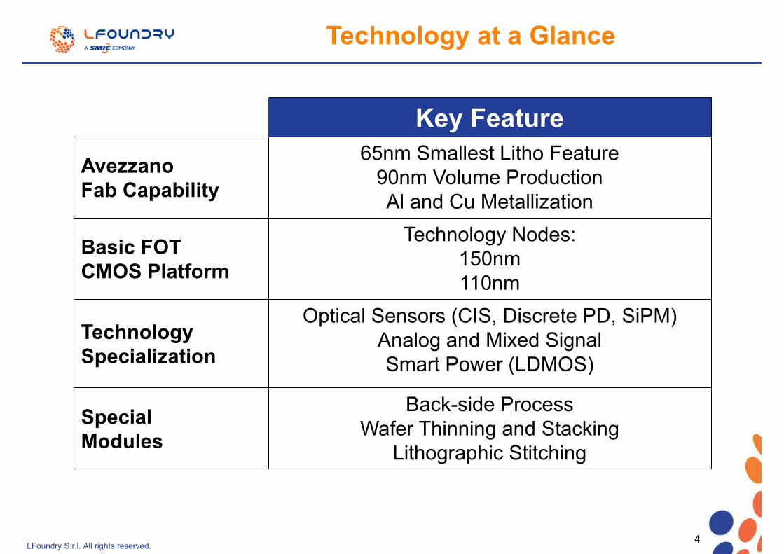
Technology at a Glance
Key Feature
Avezzano
Fab Capability
65nm Smallest Litho Feature90nm Volume ProductionAl and Cu Metallization
Basic FOT
CMOS Platform
Technology Nodes:150nm110nm
Technology
Specialization
Optical Sensors (CIS, Discrete PD, SiPM)Analog and Mixed SignalSmart Power (LDMOS)
Special
Modules
Back-side Process Wafer Thinning and Stacking
Lithographic Stitching
Confidential - LFoundry S.r.l. All rights reserved.5
Outline
• LFoundry Introduction
• Innovation Opportunities
• Development Perspective

LFoundry S.r.l. All rights reserved.6
Innovation Opportunities
6
Boundary conditions Consolidated 8” fab and manufacturing infrastructure Large volume production Technology platform till 90nm node
Innovation areas, expected effects and key contributors• Manufacturing efficiency cost reduction
- industrial-, chemistry-, electronic-engineering …..
• Process transfer and optimization production improvements- chemistry, physics, material science …..
• New module development technology added value- chemistry, material science, device physics …..
• Innovative device development broader functionality- device physics, electronic-engineering, material science …..

LFoundry S.r.l. All rights reserved.7
Optical Sensor Strategy
Infrared
Visible Light
Automotive
Industrial / Machine Vision
Medical
High Speed
Mobile
DSLR
X-ray
Photo Diode
Sensors
Highend CIS CMOS Image
Sensors
Photo Detectors,
SiPM
Standard CIS CMOS Image
Sensors
CMOS-SPAD
SiPM/Sensor-ASIC
Integration
Silicon Photo Multiplier
e.g. particle accelerator
detector magnetic
Resonance
tomography
stand alone
process
discrete
photo diode
Single Photo Avalanche Detector
Integrated inside CMOS
FSI (incl. light pipes)
Global shutter
BSI
SiPM with
e.g stacked
CMOS
HEP(high energy physic)
3D Imaging
Time of FlightSPAD
Use imaging technology & application knowhow to service full range of optical sensing: analog PDs …CIS ... to high-end 3D

LFoundry S.r.l. All rights reserved.8
CIS Pixel – New Module Developments
Metal Recess
Stitching (customer / design specific development)
wafer map
Customized Wafer Type
Deep Photo Diode
Pixel Simulation Service
Light Pipes and Optical Stack
Optimization
Microlenses
Bayer filters
Photodiodes
Access transistors
Metal layer
Max implant energy capability:
Boron 2800 keV
Phosphorous 4800 keV
Implant masking approach:
Resist up to 15:1 Aspect Ratio
Hard mask
pixel array
standard deep
optical simulation
High refractive index Polymer (n = 1.6-1.7)
ARC & stack formation
T-CAD
Isolation Implants
Modules for Global
Shutter
Buried Tungsten Light Shield
Metal ARC

LFoundry S.r.l. All rights reserved.9
Source: Yole
Hybrid Wafer Bonding for CIS

Confidential - LFoundry S.r.l. All rights reserved.10
Single Photon Detection Technologies
Single photon
detection
PMTPhotoMultiplier Tubes
APD
Avalanche Photodiode
SPAD
Single Photon Avalanche Diode
SiPM
Silicon PhotoMultiplier
SPAD / SiPM are in production at LFoundry
Main applications:• Medical (PET)
• Automotive (LIDAR, ToF)
• Industrial (ToF for quality check, Robotics)
• Science (Astronomy, Space, Dark Matter)
• Geography (City mapping by LIDAR)

LFoundry S.r.l. All rights reserved.11
Parameters
(@ room T)
NUV-HD
Cell Size 25 - 40 µm
Fill Factor 75% - 85%
Breakdown Voltage 26.5 V
Max PDE 55% @ 420 nm
Gain > 106
Peak PDE λ 410 nm
DCR (20°C) < 150 kHz/mm2 @5VoV
DiCT 20%
DeCT + AP 2%
Timing Jitter (FWHM) ~ 20ps (single cell)
LF/FBK SiPM Technology
Front Side SiPM
Key process features:• DTI (Deep Trench Isolation)
• Deep implant Photo Diode
• Quenching resistor formation
• Dielectric layers deposition/etch
• Metal line formation
• Passivation layer
SiPM technology developed by Fondazione Bruno Kessler (FBK)
at 6”, transferred to LF for large volume production at 8”, with
further development
Confidential - LFoundry S.r.l. All rights reserved.12
Outline
• LFoundry Introduction
• Innovation Opportunities
• Development Perspective
Confidential - LFoundry S.r.l. All rights reserved.13
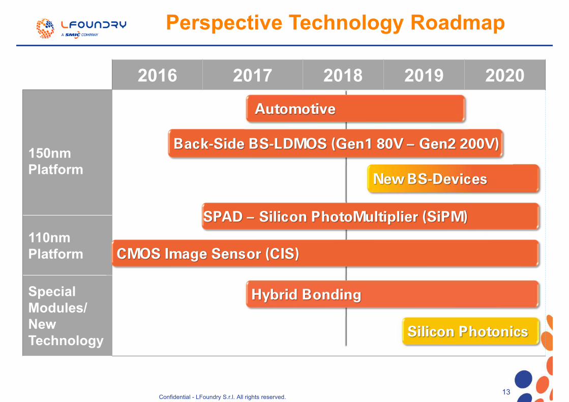
2016 2017 2018 2019 2020
150nm
Platform
110nm
Platform
Special
Modules/
New
Technology
Perspective Technology Roadmap
13
New BS-Devices
Back-Side BS-LDMOS (Gen1 80V – Gen2 200V)
Automotive
CMOS Image Sensor (CIS)
Hybrid Bonding
SPAD – Silicon PhotoMultiplier (SiPM)
Silicon Photonics

LFoundry S.r.l. All rights reserved.14
Innovative Device: BackSide p-LDMOS
n+
p-EPI
Schematic of novel
BCD technology
using wafer backside
processing
Same benefits of the SOI
approach, more cost
effective
Developed a novel BCD technology which offers all advantages of SOI technology but with lower manufacturing cost: the substrate is to a large extent removed and the devices are completed by manufacturing processes performed on the thinned wafer backside (LFoundry patent)
Confidential - LFoundry S.r.l. All rights reserved.15
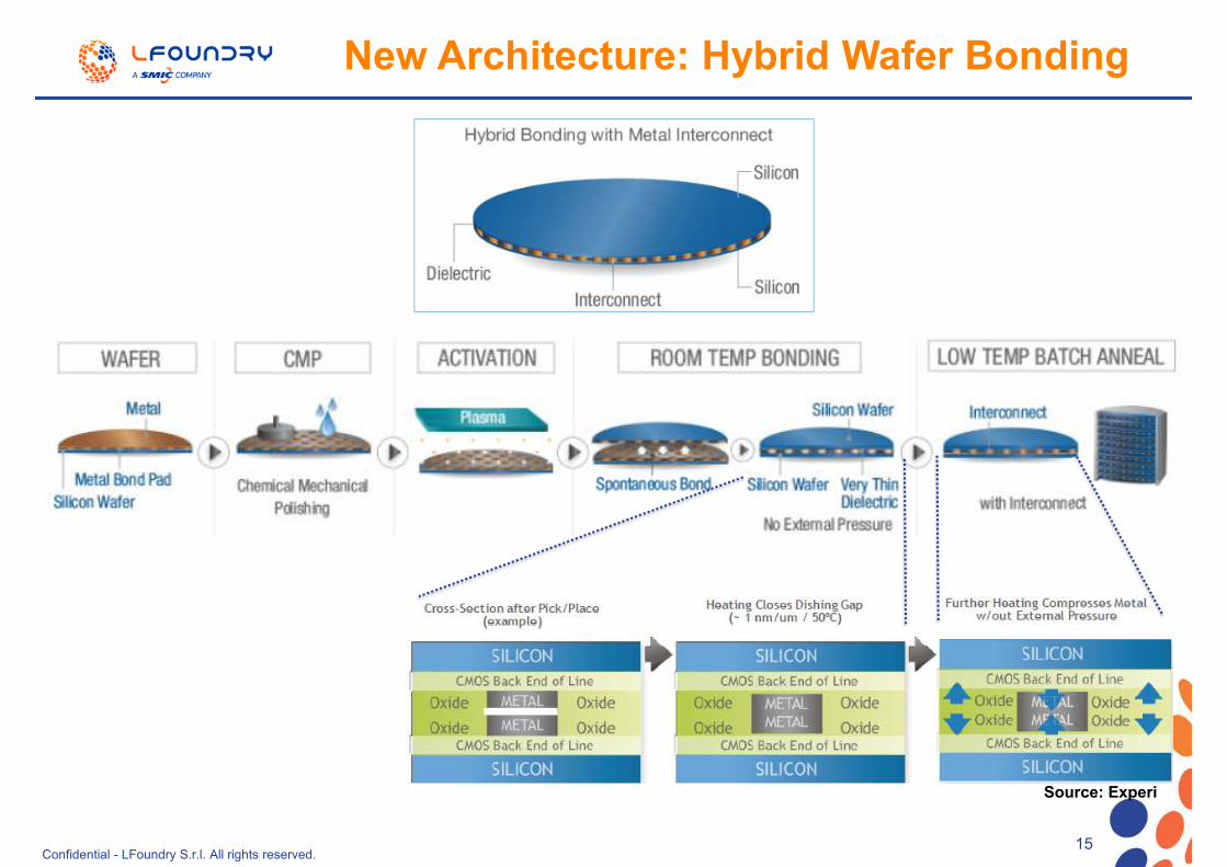
New Architecture: Hybrid Wafer Bonding
Source: Experi

LFoundry S.r.l. All rights reserved.16
Development Collaboration: Funded Project
Project Acronym End Date Objectives Partners Project Type
SATHERNUS 12/31/2020SOC multipurpose and Antenna for Avionic and Space applications
Thales Alenia Space, Elital Reg - POR FESR
SEED 31/12/2018
To develop of a state-of-the-art technology for the realization of monolithic fully-depleted radiation sensors (enabling the realization of a fast and efficient pixelated sensor with integrated electronics).
INFN MIUR - INFN
FCS_Ag.Digitale 31/12/2018 LFoundry RnD activities Only LFoundry MiSE - FCS
PhD_Italent 31/12/2019Co-funded program to facilitate PhD graduated in high tech industries
Only LFoundry MIUR - CRUI
GSTP_LF15A_Eval 31/12/2018Rad Hard characterization for LFoundry 150 nm technolgy
SITAEL, Thales Alenia Space Italia, IMT, Red Cats, UniPD ESA Tender
NANOSTREEM 31/12/2018Nanomaterials: STRategies for Safety Assessments in advanced Integrated Circuits Manufacturing
Several of the first European players in the Semiconductor Field
EU - H2020 CSA
SUPERTWIN 31/12/2018
Will develop the new generation of optical microscope systems, exploiting the properties of entangled photons to acquire images at a resolution beyond the classical Rayleigh limit of about half the photon wavelength, demonstrating a radically new line of technology for super-resolution imaging devices utilizing the principles of quantum optics.
FBK, CSEM, Ecole Polytechnique Federale de Lausanne, III-V Lab, Single Quantum, University of Bern, Institute of Physics, National Academy of Sciences of Belarus
EU - H2020 FET
Low Flux CMOS 31/01/2018 Pixel Design and Silicon provide Caeleste, ESA ESA Tender
Life BIT-MAPS 31/12/2018
Will establish a pilot plant that will demonstrate a new and never-before attempted process for the treatment of effluents from electronics and semiconductor manufacturing, introducing more efficient treatment technologies that will help reduce Tetramethylammonium hydroxide (TMAH) pollution at source.
UnivAQ, BME, BFC EU - H2020 Life
Productive 4.0 31/12/2019Electronics and ICT as enabler for digital industry and optimized supply chain management covering the entire product lifecycle.
More than 100 european partner (LE, SME, RnD center and Universities)
EU/MIUR - ECSEL

LFoundry S.r.l. All rights reserved.17
Technology for the Local Network
17
Opportunity to create a positive interactions among the local microelectronic elements and expertise (product company, design house, foundry, research center, university, institution, etc..)
Few examples:• Technology exploitation
Space application 150nm platform for ESA project (ASI)
• Technology transfer Science and industrial application Silicon Photon Multiplier (SiPM) from FBK
• Technology development Improved sensor INFN SEED project
• Technology sharing Physical characterization techniques Open Lab project
HT.III.D

THANK YOU