information for medical applications - ti.com
TRANSCRIPT

Information for Medical ApplicationsAmplifiers, Connectivity, Clocks, Data Converters, Digital Signal Processors,
Digital Temperature Sensors, Interface, Logic, Microcontrollers, Power Management
2Q 2004
Medical Imaging 3
Consumer/Personal Medical Devices 12
Biophysical Monitoring 17
Automatic External Defibrillators (AED) 24
Digital Hearing Aids 28
Connectivity 31
Logic 35
Selection Guides 36
Resources 59
Inside
R E A L W O R L D S I G N A L P R O C E S S I N GTM
System and equipment manufacturers and designers are responsible to ensurethat their systems (and any TI devices incorporated in their systems) meet allapplicable safety, regulatory and system-level performance requirements. Use ofTI devices in life support and/or safety applications is entirely at the buyer's risk,and the buyer agrees to hold TI harmless from any damages, claims, suits orexpense resulting from such use. See Important Notice on page 2.

Information for Medical Applications Texas Instruments 2Q 2004
2
Information for Medical Applications
Table of Contents
Medical ImagingUltrasound Applications and Featured Products . . . . . . . . . . . . . . . . . . . . . . . . . . . . .3
8-Channel Variable-Gain Amplifier . . . . . . . . . . . . . . . . . . . . . . . . . . . . . . . . . . . . . . . . . . . . .4
8-Channel, 10- and 12-Bit, 40- to 70-MSPS ADCs With Serialized LVDS Interface . . . . . . .5
Wideband, Voltage-Feedback Operational Amplifier With Disable . . . . . . . . . . . . . . . . . . . .5
Differential and Single-Ended Output in One Buffer . . . . . . . . . . . . . . . . . . . . . . . . . . . . . . .6
Low-Phase-Noise Clock Synthesizer With Multiplying, Dividing and Jitter Cleaning . . . . . .6
CT Scanner Applications and Featured Products . . . . . . . . . . . . . . . . . . . . . . . . . . . . .7
Precision, High-Speed Transimpedance Amplifier . . . . . . . . . . . . . . . . . . . . . . . . . . . . . . . . .8
18-Bit, 500-kSPS, Unipolar Input, Sampling ADC With Parallel Interface . . . . . . . . . . . . . . .8
Dual Current-Input, 20-Bit ADC . . . . . . . . . . . . . . . . . . . . . . . . . . . . . . . . . . . . . . . . . . . . . . . .9
8-Channel, 10-Bit, 65-MSPS, 1.8-V CMOS ADC . . . . . . . . . . . . . . . . . . . . . . . . . . . . . . . . . . .9
Magnetic Resonance Imaging (MRI) Applications and Featured Product . . . . . . .10
14-Bit, 125-MSPS ADC . . . . . . . . . . . . . . . . . . . . . . . . . . . . . . . . . . . . . . . . . . . . . . . . . . . . .10
DSPs for Imaging Applications . . . . . . . . . . . . . . . . . . . . . . . . . . . . . . . . . . . . . . . . . . . .11
High-Performance Floating-Point DSPs . . . . . . . . . . . . . . . . . . . . . . . . . . . . . . . . . . . . . . . . .11
High-Performance Fixed-Point DSPs . . . . . . . . . . . . . . . . . . . . . . . . . . . . . . . . . . . . . . . . . . .11
Consumer/Personal Medical DevicesDesign Example . . . . . . . . . . . . . . . . . . . . . . . . . . . . . . . . . . . . . . . . . . . . . . . . . . . . . . . . .12
Featured Products . . . . . . . . . . . . . . . . . . . . . . . . . . . . . . . . . . . . . . . . . . . . . . . . . . . . . . .13
16-Bit Ultra-Low-Power Microcontroller . . . . . . . . . . . . . . . . . . . . . . . . . . . . . . . . . . . . . . . .13
1.8-V, Single-Supply Operational Amplifier . . . . . . . . . . . . . . . . . . . . . . . . . . . . . . . . . . . . .14
1.25-V, 1-µA, 30-ppm/ºC Max Shunt Voltage Reference . . . . . . . . . . . . . . . . . . . . . . . . . . .14
16-Bit ADC With Input Multiplexer and Onboard Reference . . . . . . . . . . . . . . . . . . . . . . . .15
Single-Cell to 3.0/3.3-V, 20-mA, Ultra-Low Quiescent Current Charge Pump . . . . . . . . . . .15
Single-Chip Multiband RF Transceiver . . . . . . . . . . . . . . . . . . . . . . . . . . . . . . . . . . . . . . . . .16
Power-Efficient Fixed-Point DSPs . . . . . . . . . . . . . . . . . . . . . . . . . . . . . . . . . . . . . . . . . . . . .16
Biophysical MonitoringElectrocardiogram (ECG) Front End . . . . . . . . . . . . . . . . . . . . . . . . . . . . . . . . . . . . . . . .17
Device Recommendations . . . . . . . . . . . . . . . . . . . . . . . . . . . . . . . . . . . . . . . . . . . . . . . . . . .18
Pulse Oximetry . . . . . . . . . . . . . . . . . . . . . . . . . . . . . . . . . . . . . . . . . . . . . . . . . . . . . . . . . .19
Device Recommendations . . . . . . . . . . . . . . . . . . . . . . . . . . . . . . . . . . . . . . . . . . . . . . . . . . .20
Featured Products . . . . . . . . . . . . . . . . . . . . . . . . . . . . . . . . . . . . . . . . . . . . . . . . . . . . . . .21
Auto-Zero, Rail-to-Rail I/O Instrumentation Amplifier . . . . . . . . . . . . . . . . . . . . . . . . . . . . .21
Auto-Zero, Single-Supply CMOS Op Amp . . . . . . . . . . . . . . . . . . . . . . . . . . . . . . . . . . . . . .21
High-Speed, 16-Bit, Micropower Sampling ADCs . . . . . . . . . . . . . . . . . . . . . . . . . . . . . . . .22
Power-Efficient Fixed-Point DSPs . . . . . . . . . . . . . . . . . . . . . . . . . . . . . . . . . . . . . . . . . . . . .22
C2000™ Embedded Digital Signal Controller . . . . . . . . . . . . . . . . . . . . . . . . . . . . . . . . . . . .23
Automatic External Defibrillators (AED)Design Example . . . . . . . . . . . . . . . . . . . . . . . . . . . . . . . . . . . . . . . . . . . . . . . . . . . . . . . . .24
Featured Products . . . . . . . . . . . . . . . . . . . . . . . . . . . . . . . . . . . . . . . . . . . . . . . . . . . . . . .25
Low-Power, Programmable 16-Bit, 26-kSPS Dual-Channel Codec . . . . . . . . . . . . . . . . . . . .25
Important NoticeSystem and equipment manufacturers and designers are responsible to ensure that their systems (and any TI devices incorporated in theirsystems) meet all applicable safety, regulatory and system-level performance requirements. All application-related information in this publication(including application descriptions, suggested TI devices and other materials) is provided for reference only. While we have taken care to assureit is accurate, this information is subject to customer confirmation, and TI disclaims all liability for system designs and for any applicationsassistance provided by TI. Use of TI devices in life support and/or safety applications is entirely at the buyer's risk, and the buyer agrees todefend, indemnify and hold harmless TI from any and all damages, claims, suits or expense resulting from such use.
Automatic External Defibrillators (AED) (Continued)Featured Products (Continued) . . . . . . . . . . . . . . . . . . . . . . . . . . . . . . . . . . . . . . . . . . . .26
OMAP™ Processors for Portable Medical Devices . . . . . . . . . . . . . . . . . . . . . . . . . . . . . . .26
Next-Generation, Current-Mode PWM Controllers . . . . . . . . . . . . . . . . . . . . . . . . . . . . . . .26
Lowest-Noise Precision Data-Acquisition System-On-a-Chip . . . . . . . . . . . . . . . . . . . . . . .27
15-ppm/ºC Max, 100-µA, SOT23-3 Series Voltage Reference . . . . . . . . . . . . . . . . . . . . . . .27
Digital Hearing AidsDesign Example . . . . . . . . . . . . . . . . . . . . . . . . . . . . . . . . . . . . . . . . . . . . . . . . . . . . . . . . .28
Featured Products . . . . . . . . . . . . . . . . . . . . . . . . . . . . . . . . . . . . . . . . . . . . . . . . . . . . . . .30
Micropower Audio Codec . . . . . . . . . . . . . . . . . . . . . . . . . . . . . . . . . . . . . . . . . . . . . . . . . . .30
Power-Efficient Fixed-Point DSP . . . . . . . . . . . . . . . . . . . . . . . . . . . . . . . . . . . . . . . . . . . . . .30
ConnectivityUART Featured Products . . . . . . . . . . . . . . . . . . . . . . . . . . . . . . . . . . . . . . . . . . . . . . . . .31
Single and Dual UARTs . . . . . . . . . . . . . . . . . . . . . . . . . . . . . . . . . . . . . . . . . . . . . . . . . . . . .31
IR Encoder/Decoder Featured Product . . . . . . . . . . . . . . . . . . . . . . . . . . . . . . . . . . . . .31
Stand-Alone IrDA Encoder and Decoder . . . . . . . . . . . . . . . . . . . . . . . . . . . . . . . . . . . . . . . .31
1394 Featured Products . . . . . . . . . . . . . . . . . . . . . . . . . . . . . . . . . . . . . . . . . . . . . . . . . . .32
General-Purpose Link-Layer Controller . . . . . . . . . . . . . . . . . . . . . . . . . . . . . . . . . . . . . . . . .32
High-Speed Serial-Bus Link-Layer Controller . . . . . . . . . . . . . . . . . . . . . . . . . . . . . . . . . . . .32
(PCILynx-2) IEEE 1394 Link-Layer Controller . . . . . . . . . . . . . . . . . . . . . . . . . . . . . . . . . . . . .33
USB Featured Products . . . . . . . . . . . . . . . . . . . . . . . . . . . . . . . . . . . . . . . . . . . . . . . . . . .33
Industry-Leading USB 1.1 Hub Controller . . . . . . . . . . . . . . . . . . . . . . . . . . . . . . . . . . . . . . .33
USB-to-Serial Bridge . . . . . . . . . . . . . . . . . . . . . . . . . . . . . . . . . . . . . . . . . . . . . . . . . . . . . . .34
PCI Bridge Featured Product . . . . . . . . . . . . . . . . . . . . . . . . . . . . . . . . . . . . . . . . . . . . . .34
32-Bit, 66-MHz PCI-to-PCI Bridge . . . . . . . . . . . . . . . . . . . . . . . . . . . . . . . . . . . . . . . . . . . . .34
LogicLittle Logic: Single-, Dual- and Triple-Gate Logic Devices . . . . . . . . . . . . . . . . . . . . . . . . . .35
Selection GuidesAmplifiers . . . . . . . . . . . . . . . . . . . . . . . . . . . . . . . . . . . . . . . . . . . . . . . . . . . . . . . . . . . . . . .36
Comparators . . . . . . . . . . . . . . . . . . . . . . . . . . . . . . . . . . . . . . . . . . . . . . . . . . . . . . . . . . . . .42
Clock Distribution/Synthesizers . . . . . . . . . . . . . . . . . . . . . . . . . . . . . . . . . . . . . . . . . . . . . .42
Data Converters . . . . . . . . . . . . . . . . . . . . . . . . . . . . . . . . . . . . . . . . . . . . . . . . . . . . . . . . . . .43
Voltage References . . . . . . . . . . . . . . . . . . . . . . . . . . . . . . . . . . . . . . . . . . . . . . . . . . . . . . . .49
Microcontrollers . . . . . . . . . . . . . . . . . . . . . . . . . . . . . . . . . . . . . . . . . . . . . . . . . . . . . . . . . .49
Digital Temperature Sensors . . . . . . . . . . . . . . . . . . . . . . . . . . . . . . . . . . . . . . . . . . . . . . . . .50
Interface . . . . . . . . . . . . . . . . . . . . . . . . . . . . . . . . . . . . . . . . . . . . . . . . . . . . . . . . . . . . . . . . .51
Power Management . . . . . . . . . . . . . . . . . . . . . . . . . . . . . . . . . . . . . . . . . . . . . . . . . . . . . . .53
Digital Signal Processors . . . . . . . . . . . . . . . . . . . . . . . . . . . . . . . . . . . . . . . . . . . . . . . . . . .56
ResourcesApplication Reports . . . . . . . . . . . . . . . . . . . . . . . . . . . . . . . . . . . . . . . . . . . . . . . . . . . . . . . .59
TI Worldwide Technical Support . . . . . . . . . . . . . . . . . . . . . . . . . . . . . . . . . . . . . . . . . . . . . .60

Texas Instruments 2Q 2004 Information for Medical Applications
3
Medical Imaging
Ultrasound Applications
Ultrasound systems, both medical and industrial, use focal imagingtechniques to achieve imaging performance far beyond what can beachieved through a single-channel approach. Using an array ofreceivers, a high-definition image can be built by time shifting, scalingand intelligently summing echo energy. The concept of time shiftingand scaling receive signals from a transducer array provides the abilityto “focus” on a single point in the scan region. By subsequently focus-ing at different points, an image is assembled.
When initiating a scan, a pulse is generated and transmitted from eachof the eight to 512 transducer elements. These pulses are timed andscaled to “illuminate” a specific region of the body. After transmitting,
the transducer element immediately switches into receive mode. Thepulse, now in the form of mechanical energy, propagates through thebody as high-frequency sound waves, typically in the range of 1 to 15 MHz.As it does, the signal weakens rapidly, falling off as the square of thedistance traveled. As the signal travels, portions of the wave frontenergy are reflected. These reflections are the echoes that the receiveelectronics must detect. Signals reflected immediately will be verystrong, as they are from reflections close to the surface, while reflec-tions that occur long after the transmit pulse will be very weak,reflecting from deep in the body.
Because of limits on the amount of energy that can be put into thebody, the industry must develop extremely sensitive receive electronics.At focal points close to the surface, the receive echoes are strong,requiring little if any amplification. This region is referred to as thenear field. But at focal points deep in the body, the receive echoes willbe extremely weak and must be amplified by a factor of 1000 or more.This region is referred to as the far field. These regions represent thetwo extremes in which the receive electronics must operate.
Clock Distribution
High-Voltage Driver
Transducer
High-VoltageControl
CWBeamformer
DSP
TMS320C67x™
TMS320C64x™
UserInterface
Power Management
T/RSwitches
BeamformerControl System
TXBeamformer
LNA TGC ADC
Filter
RX
TI Devices
Ultrasound system block diagram.
For detailed information about TI products:
VCA8613 8-Channel Variable-Gain Amplifier 4
ADS5270/71/72/73/75/76/77 8-Channel, 10- and 12-Bit,
40- to 70-MSPS ADCs With Serialized LVDS Interface 5
OPA690 Wideband, Voltage-Feedback Operational Amplifier 5
CDCM1804 Differential and Single-Ended Output in One Buffer 6
CDC7005 Low-Phase-Noise Clock Synthesizer 6
OPA380 Precision, High-Speed Transimpedance Amplifier 8
ADS8383 18-Bit, 500-kSPS, Unipolar Input ADC 8
DDC112 Dual Current-Input, 20-Bit ADC 9
ADS5122 8-Channel, 10-Bit, 65-MSPS, 1.8-V CMOS ADC 9
ADS5500 14-Bit, 125-MSPS ADC 10
TMS320C67x™ High-Performance Floating-Point DSPs 11
TMS320C64x™ High-Performance Fixed-Point DSPs 11
To Know More
16-Channel Digital
Beamformer
LVDS IN 7
LVDS IN 7
LVDS IN 1
LVDS IN 1
ADS5270/75
PowerManagement
VCA8613
ADS1605
VCA8613 ADS5270/75
Probe/Protection
LC Delay
16-channel portable solution with Continuous Wave.
www.ti.com/medical

Information for Medical Applications Texas Instruments 2Q 2004
4
Medical Imaging
Ultrasound Applications and Featured Products
In the high-gain (far field) mode, the limit of performance is the sum ofall noise sources in the receive chain. The two largest contributors ofreceive noise are the transducer/cable assembly and the receive lownoise amplifier (LNA). In low gain (near field), the limit of performanceis defined by the magnitude of the input signal. The ratio betweenthese two signals defines the dynamic range of the system. Manyreceive chains integrate the LNA with a variable gain amplifier.
Some sort of low-pass filtering always follows the LNA+VCA combina-tion. High-end systems implement filters with more than five poleswhile low-end systems require only two poles. Many mid-range andhigh-end systems will rebuffer after filtering. In selecting an op amp,the primary considerations include signal swing, minimum and maxi-mum input frequencies, harmonic distortion and gain requirements.Analog-to-digital converters (ADCs) are typically 10- and 12-bit. SNRand power consumption are the most important issues, followed bychannel integration.
Another trend in ADCs is the implementation of an LVDS interfacebetween the ADC and the beamformer. By serializing the data comingout of the ADC, the number of interface lines can be reduced from6044 to 1024 for a 512-channel system. This reduction translates tosmaller and lower-cost PC boards, an essential part of portable imag-ing systems.
The signal assembly is accomplished with a digital beamformer. This istypically a custom-designed ASIC, but this function has been imple-mented in different forms of programmable logic. Within the beam-former the digitized signal is scaled and time delayed to create thefocusing effect in the receive chain. The properly adjusted signals arethen summed together across all receive channels and passed to theimaging system. The imaging system can be developed as a separateASIC, can be a programmable processor such as a DSP, or might be afull desktop computer.
Transmit elements require the control of 100 V to 200 V of signal swing.This is almost always accomplished with the use of high-voltage FETs.Control of the FETs can take one of two forms: on-off (push-pull) orclass-AB linear control. The most popular is the push-pull approach, asit requires a much simpler and lower-cost interface to the FETs. Theclass-AB approach dramatically improves harmonic distortion butrequires more complex drivers and consumes more power.
A wide variety of TI products have been chosen by system and equipment manufacturers for their ultrasound imaging applications,including op amps; single, dual and octal ADCs (all with fast-inputoverload recovery and excellent dynamic performance); and theVCA8613, which integrates a two-pole, low-pass filter. TI is also offering the ADS5270, an advanced 8-channel, 12-bit data converterwith serialized LVDS interface, specifically for the ultrasound market.
D(0-3)
Data
LNAIN1
LNAIN8
SerialInterface
5 x 8FIFO
CLK
CS
CW(1-10)
Attenuator
CW Processor
Attenuator
OutP(1)
OutN(1)
OutP(8)
OutN(8)
2-PoleFilter
AnalogControl
2-PoleFilter
LNA PGA
LNA PGA
8-Channel Variable-Gain Amplifier
VCA8613
VCA8613 8-channel variable-gain amplifier functional diagram.
Get samples, datasheets and app reports at:www.ti.com/sc/device/VCA8613
The VCA8613 is an 8-channel variable-gain amplifier that can meet theneeds of system designers in many of their ultrasound applications.Each channel consists of a low-noise pre-amplifier (LNA) and a variable-gain amplifier (VGA). The differential outputs of the LNA can be switchedthrough the 8 x 10 cross-point switch, which is programmable throughthe serial interface input port.
Key Features• 3-V operation• Low input noise: 1.5 nV/√Hz
__at fIN = 5 MHz
• Extremely low-power operation of 75 mW/channel• Integrated low-pass, two-pole filter, 15-MHz bandwidth• Integrated input clamp diodes• Differential output• Integrated input LNA• Readable control registers• Integrated continuous wave (CW) processor
Applications• Portable ultrasound• Portable dedicated scanners• Industrial scanners• Portable test equipment

Texas Instruments 2Q 2004 Information for Medical Applications
Medical Imaging
Ultrasound Featured Products
5
8-Channel, 10- and 12-Bit, 40- to 70-MSPS ADCs
With Serialized LVDS Interface
ADS5270, ADS5271, ADS5272, ADS5273, ADS5275,
ADS5276, ADS5277
Get samples and app reports at: www.ti.com/ads527x
The ADS527x operates from a single +3.3-V analog supply and featuresinternal references to simplify system design, or an external referencecan be used. The very low power consumption allows for the highestlevel of system integration densities. Serialized LVDS outputs reducethe number of interface lines and package size.
Key Features• 10- and 12-bit resolution• 40- to 70-MSPS sample rates• 720-mW to 1-W total power dissipation• 60-dB SNR (10-bit) and 70-dB SNR (12-bit) with fIN = 10 MHz• Serialized LVDS outputs meet or exceed requirements of ANSI
TIA/EIA-644-A standard• Internal and external references• 3.3-V analog/digital supply• Pin and format compatibility among family• Packaging: 80-pin TQFP
Applications• Portable ultrasound• Portable test equipment
6X ADCLK
1X ADCLK
S/HIN1P
ADCLK
IN1N
S/HIN2P
IN2N
S/HIN3P
IN3N
S/HIN4P
IN4N
S/HIN5P
IN5N
S/HIN6P
IN6N
S/HIN7P
IN7N
S/H ADC
ADC
ADC
ADC
ADC
ADC
ADC
ADC
IN8P
IN8N
Reference
INT/EXT REFP CS RESETREFN SDATA PD
VCM SCLK
Registers Control
PLL
OUT1P
LCLK P
OUT2P
ADCLKP
OUT3P
OUT4P
OUT5P
OUT6P
OUT7P
OUT8P
OUT1N
LCLK N
OUT2N
ADCLKN
OUT3N
OUT4N
OUT5N
OUT6N
OUT7N
OUT8N
Serializer
Serializer
Serializer
Serializer
Serializer
Serializer
Serializer
Serializer
ADS527x functional block diagram.
Wideband, Voltage-Feedback Operational
Amplifier With Disable
OPA690
Get samples, datasheets, app reports and EVMs at:www.ti.com/sc/device/OPA690
The new internal architecture of the OPA690 provides slew rate andfull-power bandwidth previously found only in wideband current-feedback op amps. Using a single supply, the OPA690 delivers highoutput currents up to 150 mA with a 150-MHz bandwidth.
Key Features• Flexible supply range:
•• +5-V to +12-V single supply•• ±2.5-V to ±5-V dual supply
• Unity-gain stable: 500 MHz (G = 1)• High output current: 190 mA• Output voltage swing: ±4.0 V• High slew rate: 1800 V/µs• Low supply current: 5.5 mA• Low disabled current: 100 µA• Wideband +5-V operation: 220 MHz (G = 2)
Applications• Video line driver• High-speed imaging channels• ADC buffers• Portable instruments• Active filters
R420 Ω
R520 Ω
C320 pF
C620 pFC4
10 µFC50.1 µF
C2
83
2
4
R1
+5 V
R2
R1
R3
0.1 µF
2.5 V
C1
VI
3.3 V
OPA690
THS1040
10 Bit40 MSPS
A +IN
A –IN
V = 1 VREF
OPA690 in a single-supply ADC driver application.
Information for Medical Applications Texas Instruments 2Q 2004
Medical Imaging
Ultrasound Featured Products
6
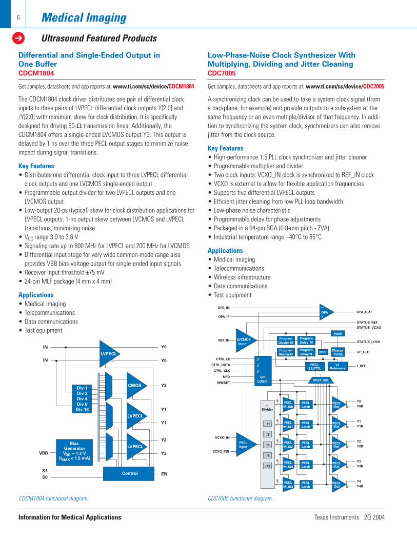
Differential and Single-Ended Output in
One Buffer
CDCM1804
Get samples, datasheets and app reports at: www.ti.com/sc/device/CDCM1804
The CDCM1804 clock driver distributes one pair of differential clockinputs to three pairs of LVPECL differential clock outputs Y[2:0] and/Y[2:0] with minimum skew for clock distribution. It is specificallydesigned for driving 50-Ω transmission lines. Additionally, theCDCM1804 offers a single-ended LVCMOS output Y3. This output isdelayed by 1 ns over the three PECL output stages to minimize noiseimpact during signal transitions.
Key Features• Distributes one differential clock input to three LVPECL differential
clock outputs and one LVCMOS single-ended output• Programmable output divider for two LVPECL outputs and one
LVCMOS output• Low-output 20-ps (typical) skew for clock distribution applications for
LVPECL outputs; 1-ns output skew between LVCMOS and LVPECLtransitions, minimizing noise
• VCC range 3.0 to 3.6 V• Signaling rate up to 800 MHz for LVPECL and 200 MHz for LVCMOS• Differential input stage for very wide common-mode range also
provides VBB bias-voltage output for single-ended input signals• Receiver input threshold ±75 mV• 24-pin MLF package (4 mm x 4 mm)
Applications• Medical imaging• Telecommunications• Data communications• Test equipment
LVPECL
IN
IN
S0
S1
Y0
Y0
Y3
Y1
Y1
Control
BiasGeneratorV – 1.3 V
(I < 1.5 mA)DD
MAX
VBB
Div 1
Div 2
Div 4
Div 8
Div 16
EN
Y2
Y2
CMOS
LVPECL
LVPECL
CDCM1804 functional diagram.
Low-Phase-Noise Clock Synthesizer With
Multiplying, Dividing and Jitter Cleaning
CDC7005
Get samples, datasheets and app reports at: www.ti.com/sc/device/CDC7005
A synchronizing clock can be used to take a system clock signal (from a backplane, for example) and provide outputs to a subsystem at thesame frequency or an even multiple/divisor of that frequency. In addi-tion to synchronizing the system clock, synchronizers can also removejitter from the clock source.
Key Features• High-performance 1:5 PLL clock synchronizer and jitter cleaner• Programmable multiplier and divider• Two clock inputs: VCXO_IN clock is synchronized to REF_IN clock• VCXO is external to allow for flexible application frequencies• Supports five differential LVPECL outputs• Efficient jitter cleaning from low PLL loop bandwidth• Low-phase noise characteristic• Programmable delay for phase adjustments• Packaged in a 64-pin BGA (0.8-mm pitch - ZVA)• Industrial temperature range –40°C to 85°C
Applications• Medical imaging• Telecommunications• Wireless infrastructure• Data communications• Test equipment
REF_IN
CTRL_LE
CTRL_DATA
CTRL_CLK
VCXO_IN
VCXO_INB
Y0B
Y1B
Y2B
Y3B
Y4B
Y0
Y1
Y2
Y3
Y4
CP_OUT
STATUS_LOCK
STATUS_VCXO
STATUS_REF
OPA_OUT
OPA_IN
OPA_IP
P Divider
I_REF
NRESET
NPD
5
5
5
5
5
SPI
LOGIC
LVCMOS
Input
Program
Divider M
Program
Delay M
Program
Divider N
Program
Delay NPFD
ChargePump
Hold
OPA
VIReference
PECL2 LVTTL
PECLLatch
PECLLatch
PECLLatch
PECLLatch
PECLLatch
MUX_SEL
PECLOut
PECLOut
PECLOut
PECLOut
PECLOut
PECL
MUX0
PECL
MUX1
PECL
MUX2
PECL
MUX3
PECL
MUX4
/1
/2
/4
/8
/16
PECL
Input
CDC7005 functional diagram.

Texas Instruments 2Q 2004 Information for Medical Applications
Medical Imaging
CT Scanner Applications
7
Texas Instruments offers several products that can meet the needs ofdesigners of medical imaging systems by enabling the measurement oflow-level currents produced by the photodiode arrays within a comput-ed tomography (CT) scanner. The OPA380 family of transimpedanceamplifiers provides high-speed (90-MHz gain bandwidth [GBW])
DigitalOutput
ADS8383Multiplexer
OPA380
OPA380
OPA380
DigitalOutput0101010
DDC112
DDC112
IIN1
IIN1
DOUT
DOUT
DIN
DIN
IIN2
IIN2
CT scanner application using the OPA380 and the ADS8383.
operation, with extremely high precision, excellent long-term stability,and very low 1/f noise. It is ideally suited for high-speed CT scannerphotodiode applications. The ADS8383 is an 18-bit 500-kSPS ADC. Thehigh-speed operation of the ADS8383 makes it well-suited for use witha multiplexer to measure multiple OPA380 channels.
The DDC112 is a complete two-channel solution for measuring photo-diodes. Its patented topology includes both the switched integratorfront end and a high speed 20-bit ADC. Two photodiodes directly con-nect to each device. A selection of internal integration capacitorsalong with optional external capacitors provides a full-scale range
from 50 pC to 1000 pC. The continuous conversion rate is 3 kSPS; single integrations can be performed as quickly as 50 µs. The simpleserial output can be daisy-chained to minimize wiring when using multiple devices.
Photodiode measurement using the DDC112 ADC.

Information for Medical Applications Texas Instruments 2Q 2004
Medical Imaging
CT Scanner Featured Products
8
18-Bit, 500-kSPS, Unipolar Input, Sampling ADC
With Parallel Interface
ADS8383
Get samples, datasheets, app reports and EVMs at:www.ti.com/sc/device/ADS8383
The ADS8383 includes an 18-bit, capacitor-based SAR ADC with inherent sample and hold. It offers a full 18-bit interface: a 16-bitoption where data is read using two read cycles or an 8-bit optionusing three read cycles.
Key Features• 500-kSPS sample rate• 18-bit NMC over temperature• Zero latency• Low power: 110 mW at 500 kHz• Onboard reference buffer• High-speed parallel interface• Wide digital supply• 8-/16-/18-bit bus transfer• Packaging: 48-pin TQFP
Applications• Medical instruments• Transducer interface• High accuracy data acquisition systems
CDAC
Output
Latches
and
3-State
Drivers
BYTE
18-/16-/8-Bit
Parallel Data
Output Bus
Conversion
and
Control Logic
Comparator
Clock
+IN
–IN
REFIN
BUSY
BUS 18/16
CONVST
CS
RD
SAR
–
+
ADS8383 functional diagram.
Precision, High-Speed Transimpedance Amplifier
OPA380
Get datasheets and app reports at: www.ti.com/sc/device/OPA380
The OPA380 transimpedance amplifier family provides high speed, highprecision and long-term stability. It exceeds the offset, drift and noiseperformance that conventional JFET op amps provide. The OPA380 iswell suited for fast control loops that detect and react to fast changesin the optical power level on a fiber.
Key Features• Over 1-MHz TIA bandwidth• Dynamic range: 5 decades• Inherent long-term stability• Output swing includes ground• Very low 1/f noise• Bias current: 50 pA (max)• Offset voltage: 25 µV (max)• Drift: 0.1 µV/ºC• Gain bandwidth: 90 MHz• Quiescent current: 6 mA• Supply range: 2.7 V to 5.5 V• Single and dual versions• Packaging: MSOP-8 and SO-8
Applications• CAT-scanner frontend• Precision current-to-voltage measurements• Optical amplifiers• Photodiode monitoring
1 MΩ
RF
100 kΩ
+5 V
OPA380
67 pF
20 mV
+
75 pF
CDIODE
–5 V
RP
(OptionalPulldownResistor)
VO
0 V to 4.9 V
Photodiode –
OP380 application diagram.

Texas Instruments 2Q 2004 Information for Medical Applications
9
Medical Imaging
CT Scanner Featured Products
Dual Current-Input, 20-Bit ADC
DDC112
Get samples, datasheets, app reports and EVMs at:www.ti.com/sc/device/DDC112
Low-level current-output devices like photosensors can be directly con-nected to the DDC112 inputs. Charge integration is continuous as eachinput uses two integrators. While one integrator is being digitized, theother is integrating. For each of its two inputs, the DDC112 combinescurrent-to-voltage conversion, continuous integration, programmablefull-scale range, analog-to-digital conversion and digital filtering toachieve a precision, wide-range digital result.
Key Features• Monolithic charge measurement ADC• Digital filter noise reduction: 3.2 ppm, rms• Integral linearity: ±0.005% Reading ±0.5-ppm FSR• High precision, true integrating function• Programmable full scale• Single supply• Cascadable output• Packaging: 28-pin SO or 32-pin TQFP
Applications• Direct photosensor digitization• CT scanner DAS• Infrared pyrometer• Liquid/gas chromatography• Blood analysis
DualSwitchedIntegrator
DualSwitchedIntegrator
DOUTDIN
DCLK
RANGE2RANGE1RANGE0
TEST CONV CLK
CAP1ACAP1A
CAP1BCAP1B
CAP2ACAP2A
CAP2BCAP2B
IN2
IN1
VREF DGNDDVDDAGNDAVDD
CHANNEL 1
CHANNEL 2
DVALID
DXMIT
Control
DigitalFilter
DigitalInput/Output
Modulator+
–
DDC112 functional diagram.
8-Channel, 10-Bit, 65-MSPS, 1.8-V CMOS ADC
ADS5122
Get samples, datasheets and app reports at:www.ti.com/sc/device/ADS5122
The ADS5122 operates from a single 1.8-V supply which offers flexibil-ity for 1.8-V and 3.3-V digital I/O. A single-ended input clock is usedfor simultaneous sampling of up to eight analog differential inputchannels. The flexible duty-cycle-adjust circuit allows the use of a non-50% clock duty cycle.
Key Features• Eight different analog input channels• 1-VPP differential input range• Int/Ext voltage reference• Analog/digital supply: 1.8 V/3.3 V• Differential nonlinearity: ±0.4 LSB• Integral nonlinearity: ±1.0 LSB• Signal-to-noise: 59 dB at fIN = 20 MHz• Power dissipation: 733 mW• Individual channel power down• Packaging: 257-lead, 0.8 ball pitch, MicroStar BGA™
Applications• Portable ultrasound• Portable instrumentation
10-Bit
ADC
3-State
Output
Buffers
D[9:0]A
10-Bit
ADC
3-State
Output
Buffers
D[9:0]H
DCASEL
AINA+
CLK
AINA–
AINH–
AINH+
IREFR
AVDD STBY OE DRVDD DVDD
Internal
Reference
Circuit
CM
AGND DRVGND DGNDBG PDREF REFT REFB CML
ADS5122 functional diagram.

Information for Medical Applications Texas Instruments 2Q 2004
Medical Imaging
Magnetic Resonance Imaging (MRI) Applications and Featured Product
10
The ADS5500 can be designed into medical MRI equipment. The 14-bitresolution provides higher SNR, which allows the designer to lower the
AMP
RF Coils
Magnet
MagnetMagnet
RF Coils
RFDetector and
Amplifier
Pulse Generation/Magnetic Field Control
PatientADS5500
THS3201, THS3202, OPA695
8/16/32 Channels Per System
DigitalProcessing
TMS320C67xTM DSPTMS320C64xTM DSPPower Management
MRI application using ADS5500 and OPA695.
magnetic field energy necessary for high-image quality. Additionally,125 MSPS allows for oversampling, which also contributes to higher
14-Bit, 125-MSPS ADC
ADS5500
S&H
Timing Circuitry
ADS5500
DigitalError
Correction
InternalReference
14-Bit Pipeline
ADC Core
OutputControl
D0I
D13
DRVDDAVDD
VIN+
VIN-
Clk+Clk-
AGND DRGND
ADS5500 functional diagram.
Get datasheets, app reports and EVMs at: www.ti.com/ads5500
The ADS5500 provides a complete converter solution. It includes a high-bandwidth linear sample-and-hold stage and internal reference. Designedfor applications demanding the highest speed and dynamic performancein very little space, the ADS5500 has low 780-mW power consumptionwith a 3.3-V single supply voltage. An internal reference is provided,and parallel CMOS-compatible output ensures seamless interfacingwith common logic. Available in a 64-pin TQFP PowerPAD™ package,the ADS5500 is specified over a –40ºC to +85ºC temperature range.
Key Features• 14-bit resolution• 125-MSPS sample rate• High SNR: 70.5 dB at 100-MHz fIN• High SFDR: 82 dB at 100-MHz fIN• 2.2-VPP differential input voltage• Internal voltage reference• 3.3-V single-supply voltage• Power dissipation: 780 mW• Packaging: 64-pin TQFP PowerPAD• Recommended op amps: THS3202, THS3201, THS4503, OPA695,
OPA847
Applications• MRI equipment• Test and measurement instrumentation• Single and multichannel digital receivers• Video and imaging

Texas Instruments 2Q 2004 Information for Medical Applications
Medical Imaging
DSPs for Imaging Applications
11
High-Performance Digital Signal Processors
TMS320C67x™ Floating-Point DSPs
Get more information at: www.ti.com/floatingpointdsps
To develop high-precision applications, TMS320C67x™ DSPs offer thespeed, precision, power savings and dynamic range to meet a widevariety of design needs. These dynamic DSPs are the ideal solution fordemanding applications such as medical imaging. TI’s C67x™ DSPs arebacked by an extensive selection of optimized algorithms and industry-leading development tools.
Key Features• Up to 1350 MFLOPS at 225 MHz (less than $0.02/MFLOPS)• C67x DSPs are 100% code-compatible with 32-bit instructions, single
and double precision• C6000™ DSP platform VelociTI™ advanced VLIW architecture• Two inter-integrated circuit (I2C) bus interfaces• Two multichannel buffered serial ports (McBSPs)• Up to 256 Kbytes of on-chip memory• 16-channel DMA controller• Up to eight 32-bit instructions executed each cycle• Eight independent, multipurpose functional units and thirty-two
32-bit registers• Industry’s most advanced DSP C compiler and assembly optimizer
maximize efficiency and performance• IEEE floating-point format• Packaging: 27/35-mm BGA and 28-mm TQFP options
Applications• Digital imaging• Medical ultrasound• Portable ultrasound equipment• CT scanners• Magnetic resonance imaging
High-Performance Digital Signal Processors
TMS320C64x™ Fixed-Point DSPs
Get more information at: www.ti.com/dsp
TMS320C64x™ DSPs offer the highest level of performance to meetthe demands of the digital age. At clock rates of up to 1 GHz, the C64x™DSPs can process information at a rate of more than 5760 MIPS. TI’sC64x DSPs are backed by an extensive selection of optimized algorithmsand industry-leading development tools.
Key Features• Highest in-class performance with devices running at clock speeds of
up to 1 GHz• TMS320C64x DSPs are 100% code-compatible with C6000™ DSPs• C64x DSPs offer up to 8000 MIPS with costs as low as $19.95• 64-channel enhanced direct memory access (EDMA) controller• Two synchronous external memory interfaces (EMIFs)• Up to three multichannel buffered serial ports (McBSPs)• PCI or Utopia Slave option• Turbo and Viterbi coprocessors• Ethernet MAC• Special instructions/capabilities: imaging, audio, accelerated video
and data• Industry’s most advanced DSP C compiler and assembly optimizer
maximize efficiency and performance• Packaging: 23/27-mm BGA options
Applications• CT medical imaging• PET medical imaging• MRI medical imaging• Ultrasound
C67x™ CPU Core
Program Fetch
Instruction Dispatch
Instruction Decode
ControlRegisters
ControlLogic
Test
In-CircuitEmulationInterrupts
L1 L2S1 S2M1 M2D1 D2
Data Path A
A Register File B Register File
Data Path B
L1P CacheDirect Mapped4 KBytes Total
L2 Memory4 Way/Banks
64 KBytes Total(C6211, C6711)
(256 KBytes forC6713)
Timer 0
Host Port Interface†16-bit
Timer 1
Enhanced DMAController
16 Channels
69 AdditionalTransfers
L1D Cache2 Way Set Associative
4 KBytes Total
Multi-channel(T1/E1)
Buffered Serial Port 1†
Multi-channel(T1/E1)
Buffered Serial Port 0†
ExternalMemoryInterface
JTAGEmulation
Control
20
32
A
D
Power Down Modes
PLL Clock Generator
GPIO
McASP 1
IIC 0
†C6713 only
†C6713 only
McASP 0or
†C6713 only
IIC 1or
or
*The C6712 DSP features a 16-bit EMIF and no HPI. All C621x and C671x devices arepin compatible. The C6713 DSP is a superset of the C6711 DSP and will include I2S, I2C and S/PDIF transmit support as well as enhanced memory space.
The C67x™ DSPs’ innovative two-level cache memory structure enables abreakthrough in system cost/performance.
Timer 0 VCP
Timer 1 TCP
Timer 2
EMIFA (64 Bits)
EMIFB (16 Bits)
MsBSP 0
MsBSP 1
UTOPIA Slave
McBSP 2
PCIor
or
HPI 32
GPIO [15:9]
GPIO [8:0]
Interrupt Selector
EnhancedDMA
Controller(64 Channel)
L2 Cache/Memory,4 Banks,
1024 KbytesTotal
TMS320C64x™DSP Core
Power-DownLogic
JTAG Emulation Control
L1D Cache 2-WaySet Associative,16 Kbytes Total
L1D Cache DirectMapped
16 Kbytes Total
PLL
The C64x™ fixed-point DSPs offer the highest level of performance to addressthe demands of the digital age.

Information for Medical Applications Texas Instruments 2Q 2004
12 Consumer/Personal Medical Devices
Design Example
Modern handheld medical devices require a sensor interface, precisionconversion circuit, flash MCU, user display, communication featuresand a power supply. In the past, to meet the conflicting electronicsrequirements of low power and high precision, handcrafted application-specific integrated circuit (ASIC) solutions were used. Glucose meterdesigners today are moving toward using off-the-shelf, ultra-low-power, mixed-signal controllers with embedded analog to meet thepower, precision, fast time-to-market and cost requirements.
This design implements a blood glucose measurement system withultra-low power consumption and numerous features. The primaryinterface is a numeric LCD requiring just 1 µA to 2 µA when active.Additional features include user input buttons, an alert buzzer and aserial communication link. A typical block diagram is shown for a
modern glucose meter implementing all features using just twodevices—the MSP430F449 ultra-low-power microcontroller and theTLV2763 amplifier with shutdown.
System designers indicate that glucose measurements can be taken inseveral ways, including optical or electrochemical methods. In electro-chemical meters, a disposable biocatalyst test strip is used to measurethe glucose content of a small blood sample. When the sample isapplied, the test strip generates a signal that is amplified and mea-sured by the operational amplifier. The operational amplifier’s output isscaled to a range that can be measured by the MSP430’s embedded12-bit analog-to-digital converter (ADC). In addition to the test stripoutput current, measurement of temperature is also required. Thechemical reaction of the test strip is temperature-sensitive. The tem-perature can be measured using the integrated temperature sensor inthe MSP430F449’s embedded 12-bit ADC.
These measurements are often logged and downloaded later to a PCfor analysis by the user and the user’s doctor. The data logging is a keyreason to use flash memory. The MSP430 can be easily programmed in-system and by the system itself. Allocating 8 Kbytes of flash memoryfor data logging is adequate for 1000 measurements, each with anassociated time stamp. The flash memory can be erased and repro-grammed 100,000 times, exceeding the life of the instrument.
All of these features can easily be implemented by glucose meter system designers using the 12-bit ADC, reference voltage, temperaturesensor and hardware serial communication interface integrated on the
For detailed information about TI products:
MSP430F43x/44x 16-Bit Ultra-Low-Power Microcontroller 13
TLV2763 1.8-V, Single-Supply Operational Amplifier 14
REF1112 1.25-V, 1-µA, 30-ppm/ºC Max Shunt Voltage Reference 14
ADS1112 16-Bit ADC With Input Multiplexer 15
TPS60310 Single-Cell to 3.0/3.3-V, 20-mA Charge Pump 15
TRF6903 Single-Chip Multiband RF Transceiver 16
TMS320C55x™ Power-Efficient Fixed-Point DSPs 16
To Know More
Sense
Bias
V_INJTAG
UserInterface
19200
3 VCR2032
32768
+
–
12-Bit ADCV
Temp_SenseREF
VCC
SD
AM/PM1 2 3 4 5 6 7 8
MSP430F4491PZ
TLV2763
www.ti.com/medical

Texas Instruments 2Q 2004 Information for Medical Applications
Consumer/Personal Medical Devices
Design Example and Featured Products
13
MSP430F43x/44x family of products. MSP430 also easily interfaces toTI’s portfolio of high-performance analog, including a broad range ofhigh-resolution data converters, precision amplifiers and powermanagement products for complete design flexibility.
For more demanding applications that require higher-resolution ADCs,system designers will find that the ADS83xx and ADS11xx familiesoffer an outstanding solution. Both families feature 16-bit resolutionand ultra-low power consumption, and they are offered in some of theindustry’s smallest footprints available today. Additionally, both fami-lies support single-channel or multichannel requirements.
As with any portable device, power management is critical. To reducepower, the first task is to shut off analog circuits when not in use.Many designers often look for the lowest-power amplifier. While lowpower consumption is key, most important is the ability to shut down.The TLV276x will typically draw current in the 10-nA range in shut-down mode. Since the meter is used only three to five times a day, it is
important to have the lowest current possible when the meter is ininactive mode.
Regarding the microcontroller, low standby-mode power consumptionand fast wake-up times are critical. The MSP430F449 features a fast-responding, high-speed clocked system with a digitally controlled oscil-lator (DCO). This system starts up in less than 6 µs to service requestsas fast as possible and then returns to standby. This extends the timein inactive mode, resulting in total reduction in power consumption.The DCO can be used in conjunction with a 32-kHz watch crystal toprovide a stable time base for an ultra-low-power embedded real-timeclock. With an active CPU current of 280 µA, the real-time clock func-tion adds less than 25 nA to the overall system power budget.
TI’s MSP430 microcontroller and high-performance analog portfolioprovide exceptional performance/cost solutions featuring ultra-lowpower consumption and high-precision performance.
Get app reports and EVMs at: www.ti.com/msp430
The MSP430F43x/44x 16-bit mixed-signal microcontroller (MCU) familyfurther improves the MSP430’s industry-leading ultra-low-power flashmemory technology—breaking the 1-µA barrier. The MSP430F43x/44xdelivers a standby mode of less than 800 nA typical, with a 32K oscil-lator, basic timer and LCD driver active. An “instant-on” digitally con-trolled oscillator (DCO) together with an integrated frequency lock loop(FLL) provides a stable, high-speed system clock in less than 6 µs. Thissaves battery power by allowing the system to stay in standby longerand utilize modern event-driven programming techniques. In activemode, the MSP430F449 consumes only 280 µA/MIPS at 2.2 V and canoperate from 1.8 V to 3.6 V over full industrial temperature range. TheMSP430F43x/44x family integrates mixed-signal peripherals thatexpand design possibilities.
Key Features• Ultra-low power consumption:
•• Active mode: 280 µA at 1 MHz, 2.2 V•• Standby mode: 0.7 µA•• Off mode (RAM retention): 0.1 µA
• Wake-up from standby mode in 6 µs• High-performance integrated analog and digital peripherals including
12-bit ADC, supply voltage supervisor, analog comparator, serialcommunication interface and hardware multiplier
• Two 16-bit PWM timers with multichannel capture/compare• Integrated LCD driver for 160 segments• Available in 80- or 100-pin quad flat pack
Applications• Handheld medical devices
MPY, MAC
8/16-bit
MAB
MDB
ACLK
JTA
G/E
EM
ACLK
LFXT1 XT2
8-MHzFLL2Osc.
Flash
32/48/60 KB
Watch-dog
15-bit
JTAG
Timer_A3
16-bit
Timer_B7
16-bit
ADC12
200 ksps
Autoscan
VREF
Temp
Comp_A Basic
Timer 1
Two
8-bit
LCDDriver
160 Seg.
RAM
1/2 KB
Power-onReset
SupplyVoltageMonitor
USART0UART/SPIUSART1
UART/SPI
Port 1/2with IRQ
Port3/4
Port5/6
RISCCPU
16-bit
SMCLK
SMCLK
MCLK
MSP430F43x typical functional diagram.
16-Bit Ultra-Low-Power Microcontroller
MSP430F43x/44x

Information for Medical Applications Texas Instruments 2Q 2004
Consumer/Personal Medical Devices
Featured Products
14
1.8-V, Single-Supply Operational Amplifier
TLV2763
Get samples, datasheets and app reports at:www.ti.com/sc/device/TLV2763
The TLV276x single-supply operational amplifiers provide 500-kHzbandwidth from only 20 µA while operating down to 1.8 V over theindustrial temperature range (±1.8 V supplies down to ±0.9 V). Themaximum recommended supply voltage is 3.6 V, which allows thedevices to be operated from two AA or AAA cells. The devices havebeen characterized at 1.8 V (end of life of two AA or AAA cells) and at2.4 V (nominal voltage of two NiCd/NiMH cells). The TLV276x familyhas rail-to-rail input and output capability, which is a necessity at 1.8 V.
Key Features• Low supply voltage: 1.8 to 3.6 V• Very low supply current: 20 µA (per channel)• Ultra-low-power shutdown mode: IQ(SHDN) = 10 nA/channel• CMOS rail-to-rail input/output• Input common-mode voltage range: –0.2 V to VDD + 0.2 V• Input offset voltage: 550 µV• Wide bandwidth: 500 kHz• Ultra-small packaging:
•• 5- or 6-pin SOT-23 (TLV2760/1)•• 8- or 10-pin MSOP (TLV2762/3)
–
+
0
2
4
6
8
10
12
14
0 0.6 1.2 1.8 2.4 3 3.6
VDD – Supply Voltage – V
SUPPLY CURRENT
vs
SUPPLY VOLTAGE
DD
I–
Su
pp
ly C
urr
ent
– µA
20
18
16
AV = 1VIC = VDD/2TA = 25˚C
TLV2763 single-supply performance.
1.25-V, 1-µA, 30-ppm/°C Max Shunt
Voltage Reference
REF1112
Get samples, datasheets and app reports at:www.ti.com/sc/device/REF1112
The REF1112 is a two-terminal shunt reference designed for power-and space-sensitive applications. It features an operating current ofjust 1 µA and is available in the SOT23-3 package.
Key Features• Wide output current range: 1 µA to 5 mA• High initial accuracy: 0.2%• Excellent specified drift performance:
30 ppm/ºC (max) from 0ºC to 70ºC50 ppm/ºC (max) from –40ºC to 85ºC
• Micro-package: SOT23-3
Applications• Medical equipment• Battery-powered instruments• Calibration circuits• Micropower current and voltage reference
RBIAS
VS
VOUT
IREF + ILOAD
IREF
RLOAD
ILOAD
RBIAS = VS – VD
ILOAD + IREF
1
2
3 NC
SOT23
GND
VO
Typical REF1112 shunt reference application.

Texas Instruments 2Q 2004 Information for Medical Applications
Consumer/Personal Medical Devices
Featured Products
15
16-Bit ADC With Input Multiplexer and
Onboard Reference
ADS1112
Get samples, datasheets and app reports at:www.ti.com/sc/device/ADS1112
The ADS1112 is a precision, continuously self-calibrating ADC withtwo differential or three single-ended channels. It uses an I2C-compatible serial interface and has two address pins that allow theuser to select one of the eight I2C slave addresses.
Key Features• Complete data acquisition system in the MSOP-10 and leadless QFN-
style packages• Measurement from two differential channels or three single-ended
channels• I2C interface: eight addresses are pin selectable• Onboard reference: 2.048 V ±0.05%, drift 5 ppm/ºC• Onboard PGA• Onboard oscillator• 16 bits, no missing codes• INL: 0.01% of FSR max• Continuous self-calibration• Single-cycle conversion• Programmable data rate: 15 SPS to 240 SPS• Power supply: 2.7 V to 5.5 V• Low current consumption: 240 µA
Applications• Medical equipment• Battery-powered instruments• Smart transmitters• Temperature measurement
Gain = 1, 2, 4, or 8
2.048-V
Reference
PGAMUX
Clock
Oscillator
∆Σ A/D
Converter
I2C
Interface
AIN0
AIN1
AIN2
AIN3
A0
A1
SCL
SDA
VDD
GND
ADS1112 block diagram.
Single-Cell to 3.0/3.3-V, 20-mA, Ultra-Low
Quiescent Current Charge Pump
TPS60310
Get samples, datasheets and app reports at:www.ti.com/sc/device/TPS60310
The TPS60310 is a high-efficiency step-up charge pump capable ofdelivering either 3.0 V or 3.3 V from a 0.9-V to 1.8-V input voltage (onealkaline, NiCd, or NiMH battery). It has an additional output capable ofproviding two times the input voltage. Requiring no inductors, the devicerequires as few as five capacitors. It has the unique ability to provide 2 mA of output current while in its snooze mode (2 µA), thus providing asignificant power savings to many ultra-low-power applications.
Key Features• Regulated output voltage with up to 40-mA current from a 0.9-V to
1.8-V source• High power-conversion efficiency, greater than 80%• Snooze mode of 2 µA still capable of supplying 2-mA output current• Additional output (dual output)• Integrated supervisor (SVS)• No inductors required, only five small capacitors
Applications• MSP430 applications• Medical instrumentation• Portable measurement • Metering applications• Portable smartcard readers
OUT15
+C(OUT1)
OUT26
C(OUT2)1 µF
R1
10PG
VIN
3
CIN
INPUT
0.9 V to 1.8 V
1SNOOZE
ON/OFF GND
9
TPS60310PG
7
8
C2FC2+
C2–
C1+
C1–
C1F
4
2
+
1 µF 1 µF
1 µF
1 µF
+
2x IN
Max. 40 mA
3.3 V ±4%
Max. 20 mA
Typical application.

Information for Medical Applications Texas Instruments 2Q 2004
Consumer/Personal Medical Devices
Featured Products
16
Single-Chip Multiband RF Transceiver
TRF6903
Get datasheet at: www.ti.com/sc/device/TRF6903
The TRF6903 single-chip solution is a low-cost multiband FSK or OOKtransceiver to establish a frequency programmable, half-duplex, bidirectional RF link. Intended for use in the North American andEuropean 315-MHz, 533-MHz, 868-MHz and 915-MHz bands, the trans-ceiver operates down to 2.2 V with low power consumption.
Key Features• ISM-band frequencies: 315, 433, 868 and 915 MHz• 2.2-V to 3.6-V operation• Low power consumption• FSK/OOK operation• Integer-N synthesizer with fully integrated voltage-controlled
oscillator (VCO)• On-chip reference oscillator and phase-locked loop (PLL)• Class-selectable power amplifier with 8-dBm typical output power• Programmable brownout detector• Clock recovery with integrated data-bit synchronizer and baud-rate
selection• Packaging: Low-profile 48-pin PQFP
Applications• Personal and portable measurement products• Handheld medical diagnostics• Battery-powered instruments• Medical equipment
*Planned availability is June 2004.
Data Clock
Transmit Data
Receive Data
Mode Select
Serial Control Data
Serial Control Clock
Serial Control Strobe
TX_DATA
RX_DATA
MODE
STDBY
DATA
CLOCK
STROBE
LNA_IN1, 2
PA_OUT
TRF6903Transceiver
+Discretes
RF Section
MSP430
Family
Microcontroller
Microcontroller
SectionAntenna
Standby
RF In
RF Out
RSSI Out (Analog Signal)RSSI_OUT
Lock Detect OutLOCK_DETECT
Brownout Detector OutDET_OUT
Learn/Hold SelectLEARN/HOLD
DCLK
Receive Data FlagRX_FLAG
System diagram for interfacing to the MSP430 microcontroller.
ProductPreviewProductPreview
Power-Efficient Digital Signal Processors
TMS320C55x™ Fixed-Point DSPs
Get samples, datasheets and app reports at: www.ti.com/c55xdsps
TMS320C55x™ DSPs offer the optimal combination of performance,peripheral options, small packaging and power efficiency in the industry.This combination gives designers an edge while designing applicationssuch as handheld medical imaging devices. TI’s C55x™ DSPs offerpower consumption as low as 0.33 mA/MHz and performance up to600 MIPS.
Key Features• Power consumption as low as 0.33 mA/MHz and performance up to
600 MIPS• Active power: 65 to 194 mW• C55x DSPs are 100% code-compatible with C5000™ DSPs• Video hardware extensions (DCT, motion estimation, pixel
interpolation)• McBSP• USB 2.0, full-speed• 16-bit HPI• 6-channel DMA• 16/32-bit EMIF• ADC• I2C• MMC/SD• UART• Special instructions: variable-length (8- to 48-bit) instructions• Packaging: MicroStar BGA™
Applications• Feature-rich, miniaturized personal and portable products• Handheld medical diagnostics• Hearing aids• Voice/speech recognition
GPIO45
3
6
6
6
2
2
1
2
7 5
2 TQFP
7 TQFP4 BGA
9 BGA
6-ChannelDMA
ExternalMemoryInterface
C55x™DSP Core
EHPI
USBPLL
DARAM64 KB
Memory
Peripheral Bus
SARAM192 KB
ROM64 KB10-Bit
A/D
USB
SystemPLL
WatchdogJTAG INT
GPIO
McBSP
McBSP
McBSP
I C2
MMC/SD
MMC/SD
2 Timers
RTC
The C55x™ DSP core is driving digital applications ranging from portableInternet appliances to high-speed wireless to power-efficient infrastructure.

Texas Instruments 2Q 2004 Information for Medical Applications
Biophysical Monitoring
Electrocardiogram (ECG) Front End
17
Biophysical Monitoring Overview
The human medical data acquisition system, in particular the patientmonitoring system, presents the challenge to designers of measuringvery small electrical signals in the presence of much larger common-mode voltages and noise. Front-end amplifiers perform the essentialconditioning that complements downstream digital processing, which inturn refines the measurement and communicates with other systems.Biophysical measurements include electrical and mechanical signalsfor general monitoring, diagnostic and scientific purposes both in clinicand non-clinic environments. Successfully meeting the signal acquisi-tion challenge requires system designers to have knowledge of the sig-nal source, good design practice and ICs with appropriate characteris-tics, features and performance.
Signal Acquisition Challenges
The action potential created by heart wall contraction spreads electricalcurrents from the heart throughout the body. The spreading electrical
currents create different potentials at different points on the body,which can be sensed by electrodes on the skin surface using biologicaltransducers made of metals and salts. This electrical potential is an ACsignal with bandwidth of 0.05 Hz to 100 Hz, sometimes up to 1 kHz. Itis generally around 1-mV peak-to-peak in the presence of much largerexternal high frequency noise plus 50-/60-Hz interference normal-mode(mixed with the electrode signal) and common-mode voltages (commonto all electrode signals).
The common-mode is comprised of two parts: 50- or 60-Hz interferenceand DC electrode offset potential. Other noise or higher frequencieswithin the biophysical bandwidth come from movement artifacts thatchange the skin-electrode interface, muscle contraction or electromyo-graphic spikes, respiration (which may be rhythmic or sporadic), electro-magnetic interference (EMI), and noise from other electronic devicesthat couple into the input. Some of the noise can be cancelled with ahigh-input-impedance instrumentation amplifier (INA), like the INA326or INA118, which removes the AC line noise common to both inputsand amplifies the remaining unequal signals present on the inputs;higher INA common-mode rejection (CMR) will result in greater rejec-tion. Because they originate at different points on the body, the left-armand right-arm ECG signals are at different voltage levels and are ampli-fied by the INA. To further reject 50- and 60-Hz noise, an operationalamplifier deriving common-mode voltage is used to invert the common-mode signal and drive it back into the patient through the right legusing amplifier A2. Only a few microamps or less are required toachieve significant CMR improvement and stay within the UL544 limit.
For detailed information about TI products:
INA326 Auto-Zero, Rail-to-Rail I/O Instrumentation Amplifier 21
OPA335 Auto-Zero, Single-Supply CMOS Op Amp 21
ADS8320/21/25 High-Speed, 16-Bit, Micropower ADCs 22
TMS320C2000™ Embedded Digital Signal Controller 22
TMS320C55x™ Power-Efficient Fixed-Point DSPs 23
To Know More
+5 V39 pF
20 kΩ
0.0015 µF
1 MΩ
5 kΩ
750 pF
A1
A3
40 kΩ
40 kΩ
390 kΩVIN–
(Right Arm)
VIN+(Left Arm)
V = V – V= 0.15 to 2 mV
IN + –
PP
IN IN
390 kΩ
390 kΩ
It is possible to omit A1, depending on
resistances.
Power Supply
Analog Circuit Common(Isolated from earth ground)+VS –VS
= (V + V )/2 IN+ IN–
390 kΩ
200 kΩ
1 µF
+5 V
INA326
+
+
+
A2
A4
+2.5-V PedestalVoltage
+
+
3.2 MΩADS8321
REF3125
OPA2335
2/2
OPA2335
1/2
OPA2335
2/2
OPA2335
1/2
A5
+
10 µFOPA335
0.1 µF
+5 V
+5 V
100 Ω
100 Ω
VREF = 2.5 V
Integrator(High-Pass Filterin the ECG Path)
To TMS320™DSP or MSP430
0.1 µF
G = 200G = 5
Inverted Common-Mode Voltage (Right Leg Drive)
Three ECG electrodes connected to patient using CMOS devices with 5-V single supply. This circuit will operate on a 3.3-V supply.
www.ti.com/medical

Information for Medical Applications Texas Instruments 2Q 2004
Biophysical Monitoring
Electrocardiogram (ECG) Front End
18
Supply Voltage
As in most other applications, the system supply voltage in biophysicalmonitoring continues the trend toward low, single-supply levels. Whilebipolar supplies are still used, 5-V systems are now common andtrending to single 3.3-V supplies. This trend presents a significant challenge for the designer faced with at least a 300-mV DC electrodepotential and emphasizes the need for a precision signal-conditioningsolution. While the following discussion concentrates on the singlesupply design, the principles involved apply to bipolar designs as well.A list of recommended single and bipolar supply devices can be foundbelow.
Frequency Response
Standard –3-dB frequency bandwidth for patient monitoring is 0.05 Hzto 30 Hz, while diagnostic grade monitoring requires 0.05 Hz to 100 Hzor more. ECG front ends must be AC coupled to remove artifacts fromthe electrode offset potential.
Electrode Potential
Because electrode potential can in practice reach ±500 mV, eliminatingthe effects of electrode potential by AC coupling is essential. A DCrestorator amplifier in a feedback configuration nulls out the DC offset.
If the left arm DC offset is +300 mV and the right arm electrode is 0-VDC, the differential input voltage is 300 mV. Because the instrumenta-tion amp has a gain of 5, 1.5 V appears at the output of the instrumen-tation amp. With a gain of 50 or more, the output amplifier would tryto drive the signal up to 75 V but never does because a feedback inte-grator applies an equal negative voltage to the reference point. Usingthis linear summing effect, the electrode offset is cancelled. The resultof this DC restorator is to turn the original DC-coupled amplifier into anAC-coupled amplifier. With the DC normal-mode voltage removed, theoutput stage can amplify the AC ECG signal without becoming saturated.
Instrumentation Amplifier Requirements• Stability in low gain (G = 1 to 10)• High common-mode rejection• Low input bias current (IB)• Good swing to the output rail• Very low offset and drift
Operational Amplifier Requirements• Low noise in high gain (Gain = 10 to 1000)• Rail-to-rail output• Very low offset and drift
Device RecommendationsDevice Type Recommended Devices Device Characteristics5-V Single SupplyInstrumentation Amplifiers INA326 110-dB CMRR at G = 100, 100-µV max offset, 0.4-µV/ºC max drift, RRIO, MSOP package
INA321 94-dB CMRR, 500-µV max offset, 7-µV/ºC drift, 40-µA supply current, RRO, MSOP packageOperational Amplifiers OPA335 5-µV max offset, 0.05-µV/ºC max drift, 350-µA max supply current, SOT23 package
OPA336 125-µV max offset, 1.5-µV/ºC drift, 32-µA max supply current, SOT23 packageData Converters ADS8325 16-bit, 100-kSPS, micropower serial output ADC, operates on 2.7 V to 5.5 V, 3mm x 3mm QFN
ADS1255, ADS1256 24-bit, 30-kSPS ADC, high effective resolution and fast conversion rate ADS1252 24-bit, 41-kSPS ADC, world’s fastest 24-bit ADC
Voltage Reference REF31xx 0.2% max initial accuracy, 15 ppm/ºC max drift, SOT23 package (1.25, 2.048, 2.5, 3.0, 3.3, 4.096 V)REF02 5-V precision voltage reference, 0.2% initial accuracy max, 10 ppm/ºC max drift, excellent line/load
regulation, low noise, SO-8 packageREF102 10-V ultra-precision voltage reference, 0.05% accuracy, 2.5ppm/ºC max drift, excellent stability and
line/load regulation, operation to 36 V, SO-8 packageDigital Signal Processor TMS320C5000™ DSP Power-efficient, high-performance DSPsPower Management bq24703 Multichemistry battery chargerBipolar SuppliesInstrumentation Amplifiers INA128 120-dB min CMRR, 5-nA max bias current, 50-µV max offset, 0.5-µV/ºC max drift, 700-µA supply current
INA118 110-dB min CMRR, 5-nA max bias current, 50-µV max offset, 0.5-µV/ºC max drift, 350-µA supply currentINA121 106-dB CMRR, 4-pA max bias current, 2-µV/ºC max drift, 200-µV offset, 0.001% max non-linearityINA126/dual INA2126 Low power: 175-µA/channel supply current, 3-µV/ºC max drift, 250-µV max offset
Operational Amplifiers OPA130 for Integrator 20-pA max bias current, 90-dB min CMRR, 120-dB min open loop gain, 1-MHz bandwidthOPA277 for Right Leg Drive Very low voltage offset and drift, wide bandwidth, low noise
Data Converters ADS8342 4-channel, 16-bit NMC, 250-kSPS, ±2.5-V input range, parallel interface in TQFP-48 packageADS7809UB 16-bit NMC, 100-kSPS, 100-dB SFDR, ±10-V input range on 5-V single supply, SPI serial interfaceDDC112 Dual current input, wide dynamic range, charge digitizing, 20-bit ADC
Digital Signal Processor TMS320C5000 DSP Power-efficient, high-performance DSPsPower Management TPS40500 DC/DC controller with 8-V to 40-V input voltage range
TPS546xx 6-A DC/DC converter with onboard power FETs

Texas Instruments 2Q 2004 Information for Medical Applications
Biophysical Monitoring
Pulse Oximetry
19
Overview
The pulse oximeter measures blood oxygenation by sensing the infraredand red light absorption properties of deoxygenated and oxygenatedhemoglobin.
It is comprised of a sensing probe attached to a patient’s earlobe, toeor finger that is connected to a data acquisition system for calculationand display of oxygen saturation level, heart rate and blood flow. Lightsources, typically light-emitting diodes, shine visible red and infraredlight. Deoxygenated hemoglobin allows more infrared light to passthrough and absorbs more red light; highly oxygenated hemoglobinallows more red light to pass through and absorbs more infrared light.The oximeter senses and calculates an amount of light at those wave-lengths proportional to the oxygen saturation (or desaturation) of thehemoglobin.
Because of the use of light in the absorbance measurement, thedesigner needs a true “light-to-voltage” conversion using current as theinput signal. The classes of photodiode amplifiers suitable for pulseoximetry applications are the classical resistor-feedback transimpedanceamplifier and the capacitor-feedback switched integrator. In eitheramplifier configuration, the resulting output voltage is read by an analog-to-digital converter and serialized for MSP430 microcontrolleror TMS320™ DSP for processing.
Signal Acquisition Challenges
The resistor-feedback amplifier circuitshown at right is the most commonbioelectric transimpedance circuit.With the amplifier used in the invert-ing configuration, the light shining ona photodiode produces a small currentthat flows to the amplifier summingjunction and through the feedbackresistor. Given the very large feedback resistor value, this circuit isextremely sensitive to changes in light intensity. For example, an inputlight signal of just 0.001 µW can produce a full-swing output.
Depending on design requirements, it can be very useful to achieveoutput swing down to or below ground. The auto-zero transimpedanceamplifier configurations shown in the next column will allow swing toground in Figure A and very close to ground in Figure B. A pull-downresistor tied to –5 V will allow swing slightly below ground to mini-mize errors as the output gets very close to zero volts.
10 MΩ
VO
Photodiode
OPA353
1 MΩ
R1
R2
+2.5 V
OPA340
or OPA350
C1
–2.5 V
C2
Photodiode
OPA335
+2.5 V
–2.5 V
IIN
ADS8320
REF3140
A. Dual Supply
1 MΩ
R1
R2
+5 V
C1
C2
Photodiode
OPA335
+5 V
IIN
–5 V
40 kΩ*
*Optional pull-down resistor to allow below ground output swing.
OPA340
or OPA350
ADS8320
REF3140
B. Single Supply
1 MΩ
RF
100 kΩ
+5 V
OPA380
67 pF
20 mV
+
75 pF
CDIODE
–5 V
RP
(OptionalPulldownResistor)
VO
0 V to 4.9 V
Photodiode –
TI’s new OPA380 is a monolithic combination of the high-speedOPA355 and auto-zero OPA335 amps. It offers 90-MHz gain bandwidthproduct and performs well as a 1-MHz transimpedance amplifier withextremely high precision (25-µV maximum offset and 0.1-µV/ºC maximum drift).

Information for Medical Applications Texas Instruments 2Q 2004
Biophysical Monitoring
Pulse Oximetry
20
Depending on design requirements, the switched integrator can be avery effective solution. TI’s IVC102 does not have the thermal noise ofa feedback resistor and does not suffer from stability problems com-monly found in transimpedance amps with a large feedback resistor.Using one photodiode with two IVC102s will eliminate dark currentand ambient light errors, as errors common to both can be subtracted.Additionally, IVC102 allows for synchronized sampling at an integermultiple of AC line frequency, giving extremely high noise rejection.Transimpedance gain can easily be changed by extending or shorteningintegration time with switch S2.
Transimpedance Amplifier Requirements• Low input bias current over temperature range of interest• Low input capacitance relative to photodiode capacitance• High gain bandwidth product• Low voltage noise• For maximum precision, low offset drift over temperature• For single-supply systems:
•• Rail-to-rail input (including 0 V) and output if operating the photodiode in photovoltaic (zero bias) mode
•• Rail-to-rail output only if operating the photodiode in photo-conductive mode (biased)
•• Shutdown and/or low supply current if battery-powered system
Design Hints
A small (< 1-pF) capacitor in the feedback loop (CF) will control gain-peaking caused by the diode capacitance. Noise (voltage-output fluc-tuation) is caused by resistor noise, amplifier and current noise, andenvironmental noise pickup (e.g., 50- or 60-Hz line noise). To minimizenoise in the circuit, the designer should choose a low-noise amplifier,select the largest practical feedback resistor, RF shield the amplifierinputs, include low-pass filtering and use good PCB layout technique.
If the photodiode shunt resistance is much larger than that of the feed-back resistor, offset voltage is not significant. If offset voltage stabilityis paramount, an auto-zero solution including the OPA335 is best.
To achieve the highest levels of precision, system designers shouldchoose the new OPA380. Designed to meet exacting transimpedanceapplication requirements, the OPA380 provides an unbeatable combi-nation of speed (85-MHz GBW, over 1-MHz transimpedance bandwidth)and precision (25-µV max offset, 0.1-µV/ºC drift, and low 1/f noise). Adiscrete alternative is to use OPA350 or OPA355, adding the OPA335 inthe integrators-stabilized transimpedance configuration for circuitsrequiring low offset and drift. Note that the addition of the OPA335integrator to a basic transimpedance amplifier will also reduce its verylow-frequency noise.
Device RecommendationsDevice Type Recommended Devices Device CharacteristicsTransimpedance Amplifier OPA380 90 GBW, over 1-MHz transimpedance BW, 25-µV max offset, 0.1-µV/ºC max drift, MSOP package
IVC102 Precision switch integrator transimpedance ampOperational Amplifiers OPA335 (5 V) 5-µV max offset, 0.05-µV/ºC max drift, 350-µA max supply current, SOT23 package
OPA735 (12 V) 5-µV max offset, 0.05-µV/ºC max drift, 750-µA max supply current, SOT23 package, 2.7-V to 12-V operationOPA336 125-µV max offset, 1.5-µV/ºC drift, 32-µA max supply current, SOT23 packageOPA350 500-µV VOS, 38-MHz, 2.5-V to 5-V supplyOPA353 High-speed single-supply rail-to-rail MicroAmplifier™ seriesOPA363/364 1.8-V high CMR, RRIO op amp with shutdownOPA703 12-V, CMOS, rail-to-rail I/O op ampOPA725 Very low noise, high-speed 12-V CMOS op amp
Data Converter DDC112 Dual current input, wide dynamic range, charge digitizing, 20-bit ADC
IIN
VB
1
2
3
4
5
6
11 12 13
Digital
Ground
Analog
Ground
Logic Low Closes Switches
9
10
14
VO
V+
V–
S1 S2
Photodiode
60 pF
30 pF
10 pF
S1
C1
C2
C3
S2
0 V
Hold Integrate Hold Reset
Positive or Negative
Signal Integration
S1
S2
IIN(t)–1 ∫ dt
CINT
VO =
IVC102

Texas Instruments 2Q 2004 Information for Medical Applications
21
Biophysical Monitoring
Featured Products
Auto-Zero, Rail-to-Rail I/O
Instrumentation Amplifier
INA326
Get samples, datasheets, app reports and EVMs at:www.ti.com/sc/device/INA326
The INA326 is a true single-supply instrumentation amplifier with verylow DC errors and input common-mode range that extends beyond thepositive and negative rails.
Key Features• Precision
•• Low offset: 100 µV (max)•• Low offset drift: 0.4 µV/ºC (max)
• True rail-to-rail I/O•• Input common-mode range: 20 mV beyond rails•• Wide output swing: Within 10 mV of rails•• Supply range: Single +2.7 V to +5.5 V•• High CMRR: 110 dB at Gain = 100
• Simple gain setting• 125ºC version: INA337• Packaging: MSOP-8
Applications• Patient monitor analog front end• Wide dynamic-range sensor measurement• High-resolution data acquisition system
R1
R2 C2
VIN–
VIN+
V+ V–
VO
G = 2(R2/R1)
INA326
INA326 block diagram.
Auto-Zero, Single-Supply CMOS Op Amp
OPA335
Get samples, datasheets and app reports at: www.ti.com/sc/device/OPA335
The OPA335 offers the ultimate combination of DC precision and lowpower consumption. It is offered in the small SOT23 package and con-sumes a maximum quiescent current of just 350 µA. In addition to having ultra-low voltage offset and drift, the OPA335 has significantlybetter bandwidth and lower 1/f noise than previous auto-zero designs.
Key Features• 5-µV max voltage offset• 0.05-µV/ºC max drift• 2-MHz gain bandwidth• Low 1/f noise• 350-µA max quiescent current• 12-V version: OPA735 (suitable for ±5-V supplies)• Packaging: SOT23
Applications• Patient monitor signal amplification• Right leg device• Precision general-purpose signal conditioning
D1
5 V
+5 V
K-TypeThermocouple
40.7 µV/˚C0 V to 5.00 V(0˚C to 500˚C)
0.1 µF
0.1 µF
REF3040
4.096 V
6.04 kΩ R1
2.94 kΩ
R2
200 Ω R6
60.4 ΩR3
6.04 kΩ R4
549 Ω R7
31.6 kΩ R5
150 kΩ R9
+ +
VO
* Auto-ZeroOp Amp
Zero Adj.
OPA335*
Typical OPA335 temperature-measurement application.

Information for Medical Applications Texas Instruments 2Q 2004
22
Biophysical Monitoring
Featured Products
SAR
SerialInterface
Comparator
S/HAmp
DCLOCK
DOUT
CS/SHDN
+IN
REF
–INCDAC
ADS8325 block diagram.
High-Speed, 16-Bit, Micropower Sampling ADCs
ADS8320, ADS8321, ADS8325
Get samples, datasheets, app reports and EVMs at:www.ti.com/sc/device/PARTnumber(Replace PARTnumber with ADS8320, ADS8321 or ADS8325)
The ADS8320/21/25 are 16-bit sampling ADCs with guaranteed specifications over a 2.7-V to 5.5-V supply range (4.75-V to 5.25-V supply range for ADS8321). The devices require very little power evenwhen operating at the full 100-kSPS data rate. At lower data rates,the devices’ high speed enables them to spend most of their time inthe power-down mode.
Key Features• 100-kSPS sampling rate (ADS8320, ADS8321)• Micropower:
•• 1.8 mW at 100 kSPS and 2.7 V (ADS8320)•• 0.3 mW at 10 kSPS and 2.7 V (ADS8320)•• 4.5 mW at 100 kSPS (ADS8321, ADS8325)•• 1 mW at 10 kSPS (ADS8321, ADS8325)
• Power down: 3 µA max (ADS8320, ADS8321)• Pin-compatible to ADS7816 and ADS7822 (ADS8325 also with
ADS8320)• Serial (SPI/SSI) interface• Packaging: MSOP-8
Applications• Battery-operated systems• Remote and isolated data acquisition• Simultaneous sampling, multichannel systems• Industrial controls• Robotics• Vibration analysis
C2000™ Embedded Digital Signal Controller
TMS320C2000™
Get app reports and EVMs at: www.ti.com/dmc
With a combination of integrated peripherals, extensive base code,application software and a variety of package types, the C2000™embedded digital signal controller is the best choice for many medicalinstrumentation systems.
TMS320C28x™ Benefits• Truly efficient C/C++ engine • Real-time general-purpose processing and debugging • Software-programmable DSP architecture for math-intensive
algorithms • Microcontroller-like interrupt-based events • Microcontroller-like peripheral integration • Field reprogrammable systems
Block diagram of typical medical instrumentation applications.
Blood PressureBody TemperatureECGOxygenPhotodiode
Comms
C2000™DigitalSignal
Controller
ADC I/O
EMIF PWM
Interface Network
Keypad
Display
PowerManagement
ExternalMemory
Sensor/Diode
Sensor/Diode
MUX

Texas Instruments 2Q 2004 Information for Medical Applications
23
Biophysical Monitoring
Featured Products
Get samples, datasheets and app reports at: www.ti.com/c55xdsps
TMS320C55x™ DSPs offer the optimal combination of performance,peripheral options, small packaging and power efficiency in the industry.This combination gives designers an edge while designing applicationssuch as handheld medical imaging devices. TI’s C55x™ DSPs offerpower consumption as low as 0.33 mA/MHz and performance up to600 MIPS.
Applications• Feature-rich, miniaturized personal and portable products• Handheld medical diagnostics• Hearing aids• Voice/speech recognition
GPIO45
3
6
6
6
2
2
1
2
7 5
2 TQFP
7 TQFP4 BGA
9 BGA
6-ChannelDMA
ExternalMemoryInterface
C55x™DSP Core
EHPI
USBPLL
DARAM64 KB
Memory
Peripheral Bus
SARAM192 KB
ROM64 KB10-Bit
A/D
USB
SystemPLL
WatchdogJTAG INT
GPIO
McBSP
McBSP
McBSP
I C2
MMC/SD
MMC/SD
2 Timers
RTC
The C55x™ DSP core is driving digital applications ranging from portable Internet appliances to high-speed wireless topower-efficient infrastructure.
Key Features• Power consumption as low as 0.33 mA/MHz and performance up to
600 MIPS• Active power: 65 to 194 mW• C55x DSPs are 100% code-compatible with C5000™ DSPs• Video hardware extensions (DCT, motion estimation, pixel
interpolation)• McBSP• USB 2.0, full-speed• 16-bit HPI• 6-channel DMA• 16/32-bit EMIF• ADC• I2C• MMC/SD• UART• Special instructions: variable-length (8- to 48-bit) instructions• Packaging: MicroStar BGA™
Power-Efficient Digital Signal Processors
TMS320C55x™ Fixed-Point DSPs

Information for Medical Applications Texas Instruments 2Q 2004
24 Automatic External Defibrillator (AED)
Design Example
analyzes the patient’s ECG and detects a shockable rhythm, the capaci-tor is charged according to energy stored in the capacitor, Wc = 1/2CV2
c;and capacitor voltage, Vc(t) = Vc(0)e–t/RC, where R = R(lead) + R(chest).
Then, following the instructions, the operator presses the shock buttonto deliver the high-voltage pulse; and current begins flowing through thebody to depolarize most of the heart cells, which often re-establishescoordinated contractions and normal rhythm. The amount of flowingcurrent is determined by the capacitor and body impedance. Theaccompanying graph shows the level of current and the length of timethe current flows through the body.
Many jurisdictions and medical directors also require that the AED recordthe audio from the scene of a cardiac arrest for post-event analysis. AllAEDs include a means to store and retrieve patient ECG patterns.
The front-end signals of the AED come from the ECG electrodes placedon the patient, which requires an instrumentation amplifier to amplifyits very small amplitude (<10 mV). The instrumentation amplifiersINA118/128/326 are designed to have:• capability to sense low-amplitude signals from 0.1 mV to 10 mV,• very high input impedance (>5 MΩ),• very low input leakage current (<1 µA),• flat frequency response of 0.1 Hz to 100 Hz and• high common-mode rejection ratio (CMRR) (>100 dB).
For detailed information about TI products:
TLV320AIC20 Low-Power, 16-Bit, 26-kSPS Dual-Channel Codec 25
OMAP5910/12 OMAP™ Processors for Portable Medical Devices 26
UCC38C4x Current-Mode PWM Controllers 26
MSC1210 Lowest-Noise Precision Data-Acquisition SoC 27
REF31xx 15-ppm/ºC Max, 100-µA, SOT23-3 Voltage Reference 27
To Know More
S1 S2
S3 S4
Display
RS232/USB
Interface
DSPMemory
OMAP59xx Processor
ARMMemory
®
Keypad
Protection
Charger
Fuel Gauge
1.8 V/3.3 V
5 V
1-Wire
H-Bridge Timing/Capacitor
Charge Control
Instrumentation/Operational Amplifiers
RS
TPA2005D1
ECGInput
ADS8321TLV320AIC12/20
INA326 orINA118
OPA335 orOPA130
C
12- to 18-V2-Ah Battery Pack
CompactFlash
MemoryCard
Serial PortMcBSP
TPS61042LED Driver
TPS61045LCD Bias
TPS3836Supervisor
TPS5130Buck
Controller
UCC38C42Current
Controller
2000-VTransformer
Circuit
DAC
ADC
ADC
Se
ria
l P
ort
DAC
TI Devices
AED block diagram.
The automated external defibrillator (AED) is a highly sophisticatedmicroprocessor-based device that monitors, assesses and automaticallytreats patients with life-threatening heart rhythms. It captures ECG signals from the therapy electrodes, runs an ECG-analysis algorithm toidentify shockable rhythms, and then advises the operator aboutwhether defibrillation is necessary. A basic defibrillator contains ahigh-voltage power supply, storage capacitor, optional inductor andpatient electrodes (see block diagram). It develops an electrical chargein the capacitor to a certain voltage, creating the potential for currentflow. The higher the voltage, the more current can potentially flow. TheAED outputs audio instructions and visual prompts to guide the opera-tor through the defibrillation procedure. In a typical defibrillationsequence, the AED provides voice prompts to instruct the user toattach the patient electrodes and starts acquiring ECG data. If the AED
www.ti.com/medical

Texas Instruments 2Q 2004 Information for Medical Applications
Automatic External Defibrillator (AED)
Design Example and Featured Products
25
The other front-end signal of the AED is the microphone input forrecording the audio from the scene of a cardiac arrest. Both ECG andmicrophone input are digitized and processed by a DSP. Most AEDdesigns use a 16-bit processor and therefore work well with 16-bitADCs to digitize ECG and voice input. The amplified ECG signal has abandwidth of 0.1 Hz to 100 Hz and requires a minimum SNR of 50 dB.The audio recording/playback signal typically has a bandwidth of 8 kHzand requires a minimum SNR of 65 dB. The microphone input alsoneeds to be amplified with a maximum programmable gain of 40 dB.The AED can have synthesized audio instruction with volume controloutput to either the headphone speaker or the 8-Ω speaker. Systemdesigners will find that the TLV320AIC20 makes the AED front-end digitization very easy and simple because it integrates two ADCs, twoDACs, a microphone amplifier, a headphone driver and an 8-Ω driverwith volume control; and it can be gluelessly interfaced to a DSP.
Cu
rre
nt
(A)
40
30
20
10
0
–10
–20
Time (ms)5 10 15 200
200J Monophasic
200J Biphasic
130J Biphasic
Typical AED drive current.
Low-Power, Programmable 16-Bit, 26-kSPS Dual-Channel Codec
TLV320AIC20
Get datasheets, app reports and EVMs at:www.ti.com/sc/device/TLV320AIC20
The TLV320AIC20 is a low-cost, low-power, highly integrated, high-performance, dual voice codec designed with new technologicaladvances. It features two 16-bit ADC channels and two 16-bit DACchannels, which can be connected to a handset, headset, speaker,microphone or a subscriber line via a programmable analog crosspoint.The TLV320AIC20’s SMARTDM™ serial port optimizes the multichannelbuffered serial port (McBSP) operation of the DSP.
Key Features• Two 16-bit oversampling ∆Σ ADCs• Two 16-bit oversampling ∆Σ DACs• Programmable sampling rate up to 26 kSPS with IIR/FIR on chip• Support maximum master clock of 100 MHz• Built-in functions:
•• Analog and digital sidetone •• Anti-aliasing filter (AAF) •• Programmable I/O gain control (PGA) •• Microphone, handset, headset amplifiers •• 8-Ω speaker driver •• Power management with hardware and software power-down
modes to 30 µW• 81-dB SNR for ADC and 78-dB SNR for DAC over 13-kHz BW• Fully compatible with TI TMS320C54x™ DSP power supplies:
•• 1.65-V to 1.95-V digital core power •• 2.7-V to 3.6-V analog
• Power dissipation:•• 20 mW at 3 V in standard operation •• 30 mW at 3 V with headset/handset drivers
• Packaging: 48-pin TQFP
Applications• ECG/EKG digitizing• Data over IP• Voice recording/playback
DAC
Internal Clock
Generator
∆ΣDAC
0 dB to –30 dB(1.5-dB Steps), –36 dB, –42 dB
Analog Sidetone–6 dB to –27 dB
Sp
eaker
8-
Ou
tpu
tH
an
dset
150-
Ou
tpu
tH
an
dset
Inp
ut
Mic
rop
ho
ne
Inp
ut
Lin
eIn
pu
tLin
e O
ut
600-
Analog Sidetone–6 dB to –27 dB
1.5 V/ 2.5 V, 2 mA
SDA SCLMCLK
LCDAC
MICBAS
CIDI+
CIDI–
LINEI+
LINEI–
MICI+
MICI–
HDSI+
HDSI–
HDSO+
HDSO–
HNSI+
HNSI–
HNSO+
HNSO–
LINEO+
LINEO–
SPKO+
SPKO–
FSD DOUT DIN SCLK FS M/S
CODEC 1
CODEC 2
+
+
∆ΣDAC
∆ΣADC
0 dB to +42 dB(1.5-dB Steps), +48 dB, +54 dB
HostPort
SMARTDM™Serial Ports
∆ΣADC
TLV320AIC20 functional block diagram.

Next-Generation, Current-Mode PWM Controllers
Offer Lowest Power and Improved Efficiency
UCC38C4x
Get samples, datasheets and app reports at:www.ti.com/sc/device/PARTnumber(Replace PARTnumber with UCC38C40, UCC38C41, UCC38C42, UCC38C43,UCC38C44 or UCC38C45)
Key Features• Fastest overcurrent protection: 35-ns delay • Low, 50-µA start-up current • Low operating current: 2.3 mA at 50 kHz • ±1-A peak output current• Rail-to-rail output swings with 25-ns rise and 20-ns fall times• ±1% initial trimmed 2.5-V error amplifier reference• Trimmed oscillator discharge current• Packaging: 8-pin DIP, 8-pin SOIC and 8-lead MSOP, which
minimizes space
Applications• Switch-mode power supplies• DC-to-DC converters• Board-mount power supplies• Telecom, industrial, medical
VREF
RT/CT
GND FB
REF
COMP
CS
OUT
VDD5-V Precision
ReferenceLow 50-µA Start-Up and 2.3-mA Operating Current
UC3842A-Based Peak Current-Mode
Architecture
35-nsCurrent Sense
Response
1-MHzOscillator
±1 A
ErrorAmplifier
UCC38C42 block diagram.
OMAP™ Processors for Portable Medical
Devices
OMAP5910, OMAP5912
Get datasheets, app reports and EVMs at: www.ti.com/sc/device/OMAP5910or www.ti.com/sc/device/OMAP5912
The dual-core OMAP59xx processor integrates a TMS320C55x™ DSPcore with a TI-enhanced ARM925 on a single chip for the optimal combination of application performance and low power consumption.This unique architecture offers an attractive solution to both DSP andARM® developers by providing the low-power, real-time signal-processing capabilities of a DSP coupled with the command and control functionality of an ARM.
The OMAP59xx processors are ideal for designers working with devicesthat require embedded applications processing in a connected environ-ment. The OMAP5912 is sampling today.
OMAP5912 Key Features• OMAP™ V1.2 • 256-KB on-chip SRAM• 200-MHz ARM 926EJ • USB-On-The-Go (OTG)• 200-MHz C55x™ v2.x DSP • (2) SD/MMC 4-bit• 100-MHz MobileDDR bus (up to 1 GB) • Compact camera interface• 50-MHz asynchronous bus (4 × 64 MB) • Self-powered RTC• 16-channel system DMA • Lead-free packaging
Applications• Portable medical devices• Asset and inventory management
FlashSRAMNAND
CF
SDRAMMobileDDR
Peripherals
OMAP v1.2 CoreTM
100 MHz
50 MHz
TrafficController/Memory I/F
16-ChannelDMA
ARM 926EJ200 MHz
®
C55x™ DSP200 MHz
LCD Ctrl 256-KBISRAM
(Frame Buff)
Secure:DES/3DES
RNGSHA1/MD5
WDTInt. Ctrl
McBSP (x2)MCSI (x2)
Timer (x8)WDTRTC
Int. CtrlµWire
ARMIO/KeyCamera I/F
LPG (x2)PWL/PWT
SD/MMC (x2)MemoryStick™CCP
USB OTG
UART (x2)UART/IrDA
MailboxI2C
McBSP232-k Timer
SPINAND Flash I/FGP Timer (x8)
GPIO32-k Sync-Timer
MMC/SDIO2
OMAP5912 functional block diagram.
Information for Medical Applications Texas Instruments 2Q 2004
26
Automatic External Defibrillator (AED)
Featured Products

Texas Instruments 2Q 2004 Information for Medical Applications
27
Automatic External Defibrillator (AED)
Featured Products
Lowest-Noise Precision Data-Acquisition
System-On-a-Chip
MSC1210
Get samples, datasheets, app reports and EVMs at:www.ti.com/sc/device/MSC1210Y2
The MSC1210 utilizes an enhanced 8051 core with on-chip Flashmemory in combination with high-performance analog and peripheralsto achieve unparalleled system performance. The integration of theanalog and digital cores gives the ability to customize the device tomeet specific requirements. It would be extremely costly and difficultto achieve this same level of flexibility and performance using multi-ple devices. The noise performance of the ADC is better than moststand-alone ADCs on the market and is significantly better than anycomparable mixed-signal device available. The accuracy and drift ofthe VREF is orders of magnitude better than other integrated peripher-als, pushing the performance envelope of digital processing to amongthe best in the industry.
Key Features• 24-bit ADC with no missing codes• 22-bits effective resolution• Eight differential/single-ended analog inputs• 8051-compatible with up to 8-MIPS operation• Up to 32-KB on-chip Flash program memory• PGA 1 to 128• Precision VREF• Packaging: 64-lead TQFP
Applications• Portable instrumentation• Intelligent sensors• Liquid/gas chromatography• Weight scales
15-ppm/°C Max, 100-µA, SOT23-3 Series
Voltage Reference
REF31xx
Get samples, datasheets and app reports at:www.ti.com/sc/device/PARTnumber(Replace PARTnumber with REF3112, REF3120, REF3125, REF3130,REF3133 or REF3140)
The new REF31xx is a cost-effective precision voltage reference family.It is well-suited to a wide range of medical applications, particularlythose requiring a combination of low power consumption and highprecision. With six different output voltage options available, theREF31xx complements a wide range of data converters and converterinput-signal levels.
Key Features• 0.2% max accuracy• 15-ppm/ºC max drift (12 typ)• ±10-mA output current• 100-µA max supply current• Packaging: SOT23-3
Applications• Medical equipment• Portable, battery-powered equipment• Data acquisition systems• Handheld test equipment• Low power spot LDO
MSC1210 block diagram.
MU
X
PGA 8051
FlashMemory
PrecisionVREF
32-Bit Accumulator
24-BitADC
120
100
80
60
40
20
0
Dro
po
ut
Vo
lta
ge
(m
V)
–15 –10 –5 5 10 15
Load Current (mA)
0
REF3112 typical dropout voltage vs. load current.
Product Voltage (V)REF3112 1.25REF3120 2.048REF3125 2.5REF3130 3.0REF3133 3.3REF3140 4.096

Information for Medical Applications Texas Instruments 2Q 2004
28 Digital Hearing Aids
Design Example
Designers of hearing aids have stringent technological requirements.Hearing aids must be small enough to fit inside or behind one’s ear, runwith extremely low power, and introduce no noise or distortion. Toachieve these requirements, current hearing aid devices consume lessthan 1 mA, operate at 1 V, and utilize less than 10 mm2 of silicon area,which usually means two or three devices stacked on top of eachother. The typical analog hearing aid consists of an amplifier with anon-linear input/output function and a frequency dependent gain.However, this analog processing suffers from a dependency on customcircuits, lack of programmability and a higher cost when compared todigital processing. Recent digital devices have reduced device costsand lowered power consumption compared to their analog counterparts.The greatest advantage offered by digital devices is their improvedprocessing power and programmability, allowing hearing aids to becustomized to a specific hearing impairment and environment. Insteadof a simple sound amplification and adjustable frequency compensa-tion, more complex processing strategies can be achieved to improvethe sound quality presented to the impaired ear. Such strategies, however, require the sophisticated processing that a DSP can provide.
Typically, hearing loss is divided into two categories: conductive hear-ing loss and sensorineural hearing loss (SNHL). A conductive hearingloss occurs when the transduction of sound through the patient’s outer
or middle ear is abnormal, and SNHL occurs when either the sensorycells in the cochlea or the neural mechanisms higher in the auditorysystem fail.
With a conductive hearing loss, sound is not properly transmittedthrough the middle or outer ear. Because sound is primarily attenuatedwith a conductive loss, amplification of sound is essentially all that isrequired to restore near-normal hearing. No special signal processingis necessary, and traditional analog hearing aids work well. However,only 5% of those inflicted with some hearing loss are attributed toconductive losses alone.
SNHL includes hearing loss that is associated with aging, as well asnoise-induced hearing loss and loss caused by drugs that are harmfulto the auditory system. Most types of SNHL appear to be caused by acochlear malfunction. SNHL is thought to be caused by damage to innerhair cells, outer hair cells or both. However, the underlying physiologyis complicated. Different people will have different pathologies, whichmeans that patients with identical audiograms will not necessarilyhave the same kind of hearing loss. Further, patients may even havediffering kinds of impairment over different frequency ranges.
The effects of SNHL usually result in lack of input in some frequencychannels, lack of sensitivity, and widened auditory filters. Theseeffects, in turn, significantly impact the listener’s perception of sound.Compared to listeners with normal hearing, listeners with SNHL willmost likely experience loudness recruitment (the range of comfortablelistening levels is compressed when compared with normal) and lossof frequency resolution, among other difficulties. These changes insound perception have significant effects on a listener’s ability tounderstand speech.
For detailed information about TI products:
AIC111 Micropower Audio Codec 30
TMS320C5402 Power-Efficient Fixed-Point DSP 30
To Know More
DSP
Power Management Battery
Clock
ADC
EEPROM
Class-DAMP
DSP-based hearing aid block diagram.
www.ti.com/medical

Texas Instruments 2Q 2004 Information for Medical Applications
Digital Hearing Aids
Design Example
29
Because SNHL is not simply a problem with the transmission of sound,but actually a problem with the processing of sound, this loss is notlikely remedied through simple amplification—making garbled soundslouder does not make them clearer. Therefore, one potentially effectiveway to help an SNHL patient is through pre-processing the signal toenhance complex tonal patterns to compensate for the hearing loss.
It is unlikely that the various manifestations of SNHL will be remediedby the same optimal treatment. Processing of the sound can makespeech more intelligible. However, the best processing algorithms willdiffer among individuals and may even change for one individual indifferent listening conditions such as a quiet room versus a noisystadium. The key to accommodating these differences is hearing aid flexibility.
Traditionally, hearing aids have been amplifiers encased in custom ear-molds fitted to the end user. The hearing aid system contains a micro-phone, an amplifier, a Zinc-Air battery and a receiver/speaker. Most ofthese amplifiers incorporate some kind of compression function, essen-tially a non-linear input/output relationship, that is used to compen-sate for loudness recruitment. Also, the gain in different frequencybands can be adjusted, and the number of frequency bands varies, butis usually two or three bands. Many of the newest aids are digitallyprogrammable, which means that although they have analog signalprocessing, the processing is controlled by digital parameters that canbe adjusted by an audiologist. In addition, some analog aids have several“programs,” or sets of parameters, for different listening environments.
Some of the digital hearing aids in the market are ASICs with program-mable coefficients. These ASICs provide a few sets of algorithms andseveral frequency bands that were not possible in typical analog devices.For example, the digital hearing aids have a combination of the follow-ing features: 2 to 14 frequency bands with adjustable crossover fre-quencies, one microphone, dual microphones for directional listening,background noise reduction, automatic gain control (AGC), speechenhancement, feedback reduction and loud sound protection. Overall,the amount of processing that can be done is impressive, especiallywhen compared with the traditional processing in an analog aid.
A DSP-based hearing aid could expand software-controlled features toinclude: frequency shaping, feedback reduction, noise reduction,binaural processing, pinna and ear canal filtering, reverberation
reduction and a provision for direct digital input from a digital tele-phone, TV or other audio devices. A programmable DSP also meansthat the hearing aid algorithms and features could be customized orchanged without changing the hardware. Hearing-aid practitionerscould economically experiment with available algorithms on a nearreal-time basis. It would even be possible to have user-selectableprograms for switching to highly processed sound in difficult listeningsituations or back to traditional, less distorted sound in quietenvironments.
The block diagram on the previous page shows the primary elementsfor a DSP-based digital hearing aid. A typical digital hearing aid con-sists of three semiconductor die stacked on top of each other: EEPROMor non-volatile memory, a digital device and an analog device. Recentadvances have allowed the integration of these modules into two oreven one semiconductor die. Due to the battery’s range of voltage from1.35 V to 0.9 V, these devices are designed to operate at 0.9 V. Someimplementations use power management to monitor battery voltageand alert the user when the battery is low and gracefully shut downthe system when the voltage drops too low. The analog device normallyincludes the sigma-delta analog-to-digital converter, microphone pre-amplifier with compression input limiting function, remote control datadecoder, clock oscillator and voltage regulator. The sigma-delta ADCtypically has a frequency range of 20 kHz with 16 bits of resolution(14-bit linear). The digital device includes the DSP, logic support func-tions, programming interface and the output stage. The output stage isnormally all digital and uses a pulse-width-modulated (PWM) outputwith Class D amplifiers that utilizes the speaker impedance to performthe analog-to-digital conversion.
Overall, the power consumption in current analog and digital hearing aidsis approximately equal. Total current consumption is about 0.7 mA to1.0 mA in the analog devices, whereas digital devices consume 0.5 mAto 0.7 mA. A 1.35-V zinc-air battery that provides around 30 to 65 mAhwith a 50-µA self-discharge current powers this system. The end-of-life voltage is about 0.9 V. Due to the increased amount of processingin the digital aids, however, a straight comparison of consumptionbetween digital and analog aids is not entirely fair. Digital aids withprocessing abilities equivalent to those of analog aids would consumeeven less power.

Information for Medical Applications Texas Instruments 2Q 2004
Digital Hearing Aids
Featured Products
30
V
MID
_FIL
T
SU
B_V
SS
AV
DD
AV
SS
_R
EF
VR
FIL
T
AV
SS
HB
_V
DD
HV
_V
SS
_P
HB
_V
SS
_M
VOUT_P
VOUT_M
AVINP
AVINM
MIC_VSUP
MIC_BIAS
VREF_BG
RST/LBM
VDD_OSC
VSS_OSC
MC
LK
IMO
DE
SC
LK
FR
AM
E
SD
OU
T
SD
IN
DVDD
DVSS
Biases Generator
BUF_DVDD
BUF_DVSS
RCFLT
∆ΣADC
Dec.Filter
and HPF
∆Σ DAC
H-BridgeSpeakerDriver
BandgapReference
DigitalInterface
Output Buffers Oscillator
POR
EX
T_R
ST
/PW
DN
MICPower and
Bias
PGA/Compressor
AIC111 functional diagram.
Micropower Audio Codec
AIC111
Get samples, datasheets, app reports and EVMs at:www.ti.com/sc/device/AIC111
The AIC111 is a micropower DSP- or microcontroller-compatible audiocodec that provides a high-performance analog interface solution forapplications such as personal medical devices—hearing aids, auralpreprocessing—and low-power headsets. The AIC111 supports a 1.3-VCMOS digital SPI interface and includes an external microphone supplyand bias, and low battery monitor and indicator.
Key Features• 400-µW full power operation at 1.3-V supply• ADC specifications:
•• Dynamic range: 87 dB•• THD: 73dB at 100 Hz to 10 kHz•• Sample rate: 40 kSPS
• Low noise PGA/gain compressor front end• On-chip low-jitter oscillator generates all internal clocks and
generates 5-MHz output DSP/microcontroller clock• SPI interface supports TMS320VC540x, TMS320VC550x DSP protocol
and MSP4330F12x microcontroller protocol• H-bridge output stage for efficient output speaker drive• 1.3-V nominal power supply• Packaging: 32-lead QFN or FlipChip bare die
Applications• Personal medical devices• Low-power headset applications
Power-Efficient Digital Signal Processor
TMS320C5402 Fixed-Point DSP
Get more information at: www.ti.com/dsp
TMS320C5402 DSP offers the power efficiency needed to sustain battery life for digital hearing aids. At 160 MHz, this processor provides an arithmetic logic unit (ALU) with a high degree of parallel-ism, application-specific hardware logic, on-chip memory and additionalon-chip peripherals. The basis of the operational flexibility and speedof this DSP is a highly specialized instruction set.
Key Features• Advanced multibus architecture with three separate 16-bit data
memory buses and one program memory bus• 40-bit ALU• Compare, select and store unit (CSSU) for the add/compare selection
of the Viterbi operator• Extended addressing mode for 8M × 16-bit maximum addressable
external program space• 16K × 16-bit on-chip RAM composed of two blocks of 8K × 16-bit
on-chip dual-access program/data RAM• Single-instruction-repeat and block-repeat for program code• Conditional store instructions• On-chip peripherals:
•• Software-programmable wait-state generator and bank-switching•• On-chip programmable phase-locked loop (PLL) clock generator
with internal oscillator or external clock source•• One 16-bit timer•• 6-channel direct memory access (DMA) controller•• Three multichannel buffered serial ports (McBSPs)•• 8/16-bit enhanced parallel host/port interface (HPI8/16)
• Power consumption control with IDLE1, IDLE2 and IDLE3 instructions• CLKOUT off control to disable CLKOUT• Packaging: 144-pin BGA and 144-pin low-profile quad flatpack (LQFP)
Applications• Digital hearing aids
BufferedSerial Port (BSP)
PLL ClockGenerator
Multichannel BufferedSerial Port (M BSP)c
S/W WaitstateGenerator
JTAGEmulation
Control
TDM Serial Port
Timer
Host PortInterface (HPI) 16/8
StandardSerial Port
MAC ALU
Power Management
17 x 17 MPY40-Bit Adder
RND, SAT
Shifter Accumulators40-Bit ACC A40-Bit ACC B
Addressing Unit8 Auxiliary Registers2 Addressing Units
40-Bit ALUCMPS Operator (Viterbi)
EXP Encoder
Program/Data ROM Program/Data RAM
DMAC54x™ DSP CPU
Ch 1Ch 2Ch 3Ch 4Ch 5
Ch 0
Program/Data BusesA(22-0)D(15-0)
Peri
pher
al B
us
40-Bit Barrel(-16, 31)
TMS320C54x™ block diagram.

Texas Instruments 2Q 2004 Information for Medical Applications
Connectivity Products
UART and IR Encoder/Decoder Featured Products
31
For detailed information about TI products:
TL16C550C/552A, TL16C750/752B Single and Dual UARTs 31
TIR1000 Stand-Alone IrDA Encoder and Decoder 31
TSB12LV32 General-Purpose Link-Layer Controller 32
TSB12LV01B High-Speed Serial-Bus Link-Layer Controller 32
TSB12LV21B (PCILynx-2) IEEE 1394 Link-Layer Controller 33
TUSB2036, TUSB2046B, TUSB2077A USB 1.1 Hub Controller 33
TUSB3410 USB-to-Serial Bridge 34
PCI2050B 32-Bit, 66-MHz PCI-to-PCI Bridge 34
To Know MoreTexas Instruments provides complete interface solutions that empoweryou to differentiate your products and accelerate time to market. TI’sexpertise in high-speed, mixed-signal circuits, system-on-a-chip integra-tion and advanced product development processes ensures you willreceive the silicon, support tools, software and technical documentationto create and deliver the best products on time and at competitive prices.
Please read on to learn about TI’s interface solutions for medical applications, including UARTs, IR encoder/decoder, 1394, USB and PCIbridges. More information on TI’s line of interface solutions can befound at interface.ti.com
Single and Dual UARTs
TL16C550C, TL16C552A, TL16C750, TL16C752B
Get samples, datasheets and EVMs at:www.ti.com/sc/device/PARTnumber(Replace PARTnumber with TL16C550C, TL16C552A, TL16C750or TL16C752B)
A wide portfolio of space-saving, performance-enhancing UARTS arepin-for-pin compatible with many leading UART manufacturers’ devices.The TL16C550C is a 3.3-V/5-V single-channel, industry-standard UARTthat performs serial-to-parallel and parallel-to-serial data conversion.The TL16C552A enhanced, dual-channel device serves two serialinput/output interfaces simultaneously and adds a bi-directional lineprinter port. The TL16C750 offers a 64-byte FIFO with 16- or 64-byteFIFO programmability. The TL16C752B is a high-performance, dualUART with a 64-byte FIFO capable of 2.9-Mbps data transfer.
Key Features• Single-, dual- and quad-channel devices available• Hardware and software auto-flow control• Programmable sleep mode and low-power mode• Industrial temperature range available• Choice of 5-V and 3.3-V supply
Applications• Medical monitors and scanners
8-Bit Parallel SignalUART
TL16C550C
RS-232
SN75C3238
RS-232
SN75C3243
UART
TL16C550C8-Bit Parallel Signal
Serial Signal
Typical UART system.
Stand-Alone IrDA Encoder and Decoder
TIR1000
Get samples, datasheets, app reports and EVMs at:www.ti.com/sc/device/TIR1000
The TIR1000 serial infrared (SIR) encoder/decoder is a CMOS devicewhich encodes and decodes bit data in conformance with the IrDAspecification. A transceiver device is needed to interface to the photo-sensitive diode (PIN) and the light-emitting diode (LED). A UART isneeded to interface to the serial data lines.
Key Features• Adds infrared (IR) port to UARTs• Compatible with IrDA and Hewlett Packard serial infrared (HPSIR)• Provides 1200 bps to 115 kbps data rate• Operates from 2.7 V to 5.5 V• Provides simple interface with UART• Decodes negative or positive pulses• Available in two 8-terminal PSOP packages
Applications• Medical instrumentation
RESET
IR_RXD
16XCLK
U_TXD
U_RXD
IR_TXD
Decoder
Encoder
TIR1000 functional block diagram.
www.ti.com/medical

Information for Medical Applications Texas Instruments 2Q 2004
Connectivity Products
1394 Featured Products
32
TSB12LV32 block diagram.
MA[0:6]
MD[0:15]
BCLK
Byte Stacker8/16 to 32
Bits
7
16
7
32
Address7
Data32
FIFO
CFRControl
IRF32
CTL[0:1]
Hos
t Int
erfa
ce
DataMover(DM)
DMD[0:15]
DM Control
16
Data-Mover
Port
32DM IT/AT
– 2 SCLK
Microcontroller Interface
MCAMCS
Status
2K ATF2K GRF
Pack
et R
oute
r Con
trol
32 DM IR/AR
ATF
GRF
DMCLK
D[0:7]
LREQ
SerialBus
LPS
LinkOn
MRW
ARF32
ATF32
Link
Cor
e
HostInterface
ExternalMemory
Transmitter
Cycle Timer
Cycle Monitor
CRC
Receiver
Internal Configuration Registers (CFR)
GRF
ITF
ATF
FIFO
HostProcessor
Hos
t Int
erfa
ce
Phys
ical
Inte
rfac
e
SerialBus
Link Core
TSB12LV01B block diagram.
High-Speed Serial-Bus Link-Layer Controller
TSB12LV01B
Get samples, datasheets and app reports at:www.ti.com/sc/device/TSB12LV01B
The TSB12LV01B is an IEEE 1394-1995 high-speed serial-bus link-layercontroller that allows for easy integration into an I/O subsystem. TheTSB12LV01B provides a high-performance 1394 interface with thecapability of transferring data between the 32-bit host bus, the 1394PHY-link interface, and external devices connected to the local businterface. The link-layer controller provides the control for transmittingand receiving 1394 packet data between the FIFO and PHY-linkinterface at rates of 100, 200 and 400 Mbps.
Key Features • Compliant with IEEE 1394-1995 standards for high-performance
serial bus• Link core:
•• Transmits and receives correctly formatted 1394 packets •• Supports asynchronous and isochronous data transfers •• Contains asynchronous, isochronous, and general-receive FIFOs
totaling 2 KB • PHY interface supports transfer speeds of 100, 200 and 400 Mbps • Host bus interface provides chip control with directly addressable
registers and is interrupt-driven to minimize host polling • Single 3.3-V supply operation with 5-V tolerance using 5-V bias
terminals• Packaging: 100-pin PZT for –40ºC to 85ºC operation
Applications• Vision systems• Instrumentation• Command and control• IDB-1394
General-Purpose Link-Layer Controller
TSB12LV32
Get samples, datasheets and app reports at:www.ti.com/sc/device/TSB12LV32
The TSB12LV32 (GP2Lynx) is a high-performance, general-purpose 1394alink-layer controller (LLC) that can transfer data between a host control-ler, the 1394 PHY-link interface and external devices connected to thelocal bus interface. The LLC provides the control for transmitting andreceiving 1394 packet data between the microcontroller interface andthe PHY-link interface via internal 2-KB FIFOs at rates up to 400 Mbps.
Key Features • Compliant with IEEE 1394-1995 standards and P1394a supplement
for high-performance serial bus • Link core:
•• Transmits and receives correctly formatted 1394 packets •• Supports asynchronous and isochronous data transfers •• Contains 2-KB asynchronous-transmit and 2-KB general-receive FIFOs
• PHY interface supports transfer speeds of 400, 200 or 100 Mbps • Glueless interface to 68000 and ColdFire® microcontrollers/
microprocessors • Programmable microcontroller interface with 8-bit or 16-bit data
bus, multiple modes of operation including burst mode and clockfrequency to 60 MHz
• 8-bit or 16-bit data-mover port (DM Port) supports isochronous,asynchronous and streaming transmit/receive from an unbufferedport at a clock frequency of 25 MHz
• Single 3.3-V supply operation with 5-V tolerance using 5-V biasterminals
• Packaging: High-performance 100-pin PZ
Applications • Vision systems• Instrumentation• Command and control• IDB-1394

Texas Instruments 2Q 2004 Information for Medical Applications
Connectivity Products
1394 and USB Featured Products
33
(PCILynx-2) IEEE 1394 Link-Layer Controller
TSB12LV21B
Get samples, datasheets and app reports at:www.ti.com/sc/device/TSB12LV21B
The TSB12LV21B (PCILynx-2) provides a high-performance IEEE 1394-1995 interface that can transfer data between the 1394 PHY-link inter-face, the PCI bus interface and external devices connected to the localbus interface. The 1394 PHY-link interface provides the connection tothe 1394 physical layer device; it is supported by the onboard link-layercontroller (LLC). The LLC provides the control for transmitting andreceiving 1394 packet data between the FIFO and PHY-link interface atrates of 100, 200, and 400 Mbps.
Key Features• IEEE standard for 1394-1995 and 1212-1991 compliant• Supports IEEE 1394-1995 link-layer control• PCI local bus specification Rev. 2.1 compliant• 3.3-V core logic while maintaining 5-V-tolerant inputs• Performs the function of 1394 cycle master• Provides 4 Kbytes of configurable FIFO RAM
Applications• 1394 embedded host controller• 1394 PC host controller• Instrumentation• Command and control
HostCPU
1394 Peripheral
DevicesPersonal Computer
PCIHost
Bridge
LocalMemory
PCILynx-2TSB12LV21B
VideoController
IDEController
13943-Port
PhysicalLayer
PCIExpansion
ROM
DMAChannelControl(SRAM)
UserDefinedFunction
(AUX)
ZVPort
(Video)
1394DesktopCamera
1394CD ROM
1394LaserPrinter
1394DigitalVCR
1394Video CableSet Top Box
PCI Bus
Local Bus
Typical application featuring the TSB12LV21B.
Industry-Leading USB 1.1 Hub Controller
TUSB2036, TUSB2046B, TUSB2077A
Get samples, datasheets, app reports and EVMs at:www.ti.com/sc/device/PARTnumber(Replace PARTnumber with TUSB2036, TUSB2046B or TUSB2077A)
TI offers a variety of USB hub ICs for various applications that are fullycompliant to the USB 1.1 specification and are on the USB-IF integra-tor’s list.
Key Features• Self- and bus-powered support• USB suspend/resume operation support• Custom VID and PID with external serial EEPROM• ESD filtering for babble, overcurrent, reset, bus-powered inputs• TUSB2036: Pin-selectable configuration for 2 or 3 ports• TUSB2046B: 4-port hub• TUSB2077A: 7-port hub, self-powered for 7 ports and bus-powered
for 4 ports
Applications• Stand-alone hub boxes• Motherboard• Monitor with embedded control functions• Embedded in peripheral (printer, scanners)• All-in-one control unit
V1.1X-cvr
DPO DMO
V1.1X-cvr
V1.1X-cvr
DM1DP1DMn
Downstream Ports
Upstream Port
DPn
HubRepeater
SIE InterfaceLogic
SIE
ClockCircuits
OSC/PLL
Suspend/ResumeLogic and
Frame TimerSUSPND
XTAL
RESET
Hub/DeviceCommandDecoder
SerialEEPROMInterface
Hub PowerLogic
Port 1Logic
Port 1Logic
EXTMEM
EEDATA/GANGED
EECLK
Device SpecificControl Signals
BUSPWR
OVRCUR1 - OVRCURn
PWRON1 - PWRONnn
n
m
Port 0Logic
TUSB20xx block diagram.

Information for Medical Applications Texas Instruments 2Q 2004
Connectivity Products
USB and PCI Bridge Featured Products
34
USB-to-Serial Bridge
TUSB3410
Get samples, datasheets, app reports and EVMs at:www.ti.com/sc/device/TUSB3410
The TUSB3410 provides an easy way to move your serial-based legacydevice to a fast, flexible USB interface by bridging between a USBport and an enhanced UART serial port. The TUSB3410 contains allthe necessary logic to communicate with the host computer using theUSB bus.
Key Features• USB full-speed compliant: data rate of 12 Mbps• 8052 microcontroller with 16 Kbytes of RAM that can be loaded
from the host or from external onboard memory via an I2C bus• Integrated, enhanced UART features including:
•• Programmable software/hardware flow control•• Automatic RS-485 bus transceiver control, with and without echo•• Software-selectable baud rate from 50 to 921.6 kbaud•• Built-in, two-channel DMA controller for USB/UART bulk I/O
• An evaluation module can jump-start your USB development, or youcan use it as a complete USB-to-RS-232 converter
Applications• Handheld meters• Health metrics/monitors• Any legacy serial device that needs to be upgraded to USB
In
Out
SIN
SOUT
USB
Legacy
Serial
Peripheral
Host
(PC or OTG DRD)TUSB3410
TUSB3410 data flow.
32-Bit, 66-MHz PCI-to-PCI Bridge
PCI2050B
Get samples and datasheets at: www.ti.com/sc/device/PCI2050B
The PCI2050B PCI-to-PCI bridge provides a high-performance connec-tion path between two peripheral component interconnect (PCI) busesoperating at a maximum bus frequency of 66 MHz. Transactions occurbetween masters on one and targets on another PCI bus, and the PCI2050Ballows bridged transactions to occur concurrently on both buses.
Key Features• Two 32-bit, 66-MHz PCI buses• Compliant with PCI-to-PCI Bridge Spec, Rev 1.1• 3.3-V core logic with universal PCI interfaces compatible with 3.3-V
and 5-V PCI signaling environments• Internal two-tier arbitration for up to nine secondary bus masters and
supports an external secondary bus arbiter• Ten secondary PCI clock outputs• Burst data transfers with pipeline architecture to maximize data
throughput in both directions• CompactPCI hot-swap functionality• 208-terminal PDV, 208-terminal PPM or 257-terminal MicroStar
BGA™ package
Applications• Server add-ons• Data storage• System control backplanes
Typical PCI2050B application.
PCI Option Card
CPU Memory
HostBridge
PCI2050B
PCI Bus 0
PCI Bus 1
Host Bus
PCI Option Slot
PCI2050B PCIDevice
PCIDevice
PCIDevice
PCIDevice
PCI Bus 2
(Option)
PCI Option Card

Texas Instruments 2Q 2004 Information for Medical Applications
Logic 35
Little Logic offers voltage-range operating levels from 5.5-V all the waydown to sub-1-V VCC and can be utilized with AHC/T (5-V), LVC (3.3-V),and AUC (1.8-V) product families. Designs that require signal switchingcan take advantage of TI’s CBT Little Logic families. The CBT devicesprovide bus switch solutions in a variety of options including CBTD for
Little Logic4,00 mm
0,65 mm
2,95 mm
Little Logic3,1 mm
0,50 mm2,0 mm
Little Logic2,80 mm
0,95 mm
2,90 mm
Little Logic 2,10 mm
0,65 mm2,0 mm
1,4 mm
0,9 mm
0,5 mm
DCT (SM-8)
(Actual Size)
DCU (US-8)
(Actual Size)
DBV (SOT-23)
(Actual Size)
DCK (SC-70)
(Actual Size)
NanoStarTM
(YEP)5-pin or 6-pin
(Actual Size)
5-pin or 6-pin 5-pin or 6-pin
NanoFreeTM
(YZP)1,9 mm
0,9 mm
0,5 mmNanoStarTM
(YEP)8-pin
(Actual Size)
NanoFreeTM
(YZP)
Space-saving Little Logic packages.
Key Features• 1.8-V to 5.5-V optimized performance• Sub 1 V operation with AUC Little Logic• World’s smallest package NanoStar™• Low-voltage bus switching (CBTLV)• Pb-Free offering• Packaging: See below
Applications• Portable media device• PDA/pocket PC• Cellular phone• Computing
1The propagation delay is the calculated RC time constant of the typical on-state resistance of the switch and the specifiedload capacitance, when driven by an ideal voltage source (zero output impedance). The value listed is a maximum.2The FET switch has no output drive. The drive current at the output terminal is determined by the drive current of the deviceconnected at the input terminal of the FET switch.
Little Logic Performance ComparisonsOperating Optimized Propagation Output Input
Voltage Range Voltage Delay, tpd Drive Tolerance IOFF
Family (V) (V) (ns) (typ) (mA) (V) ProtectionAUC 0.8 to 2.7 1.8 2.0 8 3.6 YesLVC 1.65 to 5.5 3.3 3.5 24 5.5 YesAHC 2.0 to 5.5 5.0 5.0 8 5.5 NoAHCT 4.5 to 5.5 5.0 5.0 8 5.5 NoCBT 4.5 to 5.5 5.0 0.251 —2 5.5 YesCBTD 4.5 to 5.5 5.0 0.251 —2 5.5 YesCBTLV 2.3 to 3.6 3.3 0.251 —2 3.6 Yes
5-V to 3.3-V translation and CBTLV for low-voltage operation. LittleLogic provides packaging options in 5-, 6- and 8-pin packages, includ-ing NanoStar™ and NanoFree™, that are 70% smaller than the 5-pinSC-70 and 13% smaller than any other logic package available today.
Little Logic: Single-, Dual- and Triple-Gate Logic DevicesGet samples, datasheets and app. reports at: www.ti.com/littlelogic

Information for Medical Applications Texas Instruments 2Q 2004
36 Selection Guides
Amplifiers
Voltage-Controlled AmplifiersPower Per
Voltage Noise Low-Noise Channel Gain Range Analog SupplyDevice Channels (nV/√Hz
__) Pre-Amplifier (mW) (dB) (V) Package Price1
VCA2611 2 1 Yes 205 40 5.0 TQFP-48 9.97VCA2616 2 1 Yes 205 40 5.0 TQFP-48 9.75VCA2619 2 5.9 No 120 50 5.0 TQFP-32 7.97VCA8613 8 1.5 Yes 88 40 3.0 TQFP-64 25.40
1Suggested resale price in U.S. dollars in quantities of 1,000. New devices are listed in bold red.
Difference AmplifiersOffset
Spec1 Offset Drift CMRR BW Power IQTemp (µV) (µV/ºC) (dB) (MHz) Output Voltage Supply (mA)
Device Description Range Ch. Gain (max) (max) (min) (typ) Swing (V) (min) (V) (max) Package(s) Price3
General PurposeINA132 Micropower, High-Precision I 1, 2 1 250 5 76 0.3 (V+) – 1 to (V–) + 0.5 +2.7 to +36 0.185 DIP, SO 0.99INA133 High-Precision, Fast I 1, 2 1 450 5 80 1.5 (V+) – 1.5 to (V–) + 1 ±2.25 to ±18 1.2 SOIC-8/-14 0.99INA143 High-Precision, G = 10 or 1/10 I 1, 2 10, 1/10 250 3 86 0.15 (V+) – 1 to (V–) + 0.5 ±2.25 to ±18 1.2 SOIC-8/-14 0.99INA145 Resistor Programmable Gain I 1, 2 1-1000 1000 102 76 0.5 (V+) – 1 to (V–) + 0.5 ±1.35 to ±18 0.7 SOIC-8 1.40INA152 Excellent Swing to Rail I 1 1 750 5 86 0.7 (V+) – 0.2 to (V–) + 0.2 +2.7 to +20 0.65 MSOP-8 1.10INA154 High-Speed, Precision, G = 1 I 1 1 750 20 80 3.1 (V+) – 2 to (V–) + 2 ±4 to ±18 2.9 SOIC-8 0.99INA157 High-Speed, G = 2 or 1/2 I 1 2, 1/2 500 20 86 4 (V+) – 2 to (V–) + 2 ±4 to ±18 2.9 SOIC-8 0.99AudioINA134 Low Distortion: 0.0005% I 1, 2 1 1000 22 74 3.1 (V+) – 2 to (V–) + 2 ±4 to ±18 — SOIC-8/-14 0.99INA137 Low Distortion, G = 1/2 or 2 I 1, 2 2, 1/2 1000 22 74 4 (V+) – 2 to (V–) + 2 ±4 to ±18 2.9 SOIC-8/-14 0.99High Common-Mode VoltageINA117 ±200-V CM Range I 1 1 1000 20 86 0.2 (V+) – 5 to (V–) + 5 ±5 to ±18 — SOIC-8 2.70INA146 ±100-V CM Range, Prog. Gain I 1 0.1-100 5000 1002 70 0.55 (V+) – 1 to (V–) + 0.15 ±1.35 to ±18 0.7 SOIC-8 1.60INA148 ±200-V CM Range, 1-MΩ Input I 1 1 5000 1002 70 0.1 (V+) – 1 to (V–) + 0.25 ±1.35 to ±18 0.3 SOIC-8 1.95
1I = –40ºC to +85ºC.2Denotes single supply.3Suggested resale price in U.S. dollars in quantities of 1,000.
Current Shunt MonitorsOffset IQ Per
Offset Drift CMRR BW Power Ch.Gain (µV) (µV/°C) (dB) (MHz) Output Voltage Supply (mA)
Device Description Ch. (µV) (max) (max) (min) (typ) Swing (V) (min) (V) (max) Package(s) Price1
High-Side Current Shunt MonitorsINA138 36V max 1 200 1000 1 100 0.8 0 to (V+) –0.8 +2.7 to 36 0.045 SOT23-5 0.95INA139 High-Speed, 40V max 1 1000 1000 1 100 4.4 0 to (V+) –0.9 +2.7 to 40 0.125 SOT23-5 0.95INA168 60V max 1 200 1000 1 100 0.8 0 to (V+) –0.8 +2.7 to 60 0.045 SOT23-5 1.15INA169 High-Speed, 60V max 1 1000 1000 1 100 4.4 0 to (V+) –0.9 +2.7 to 60 0.125 SOT23-5 1.15INA170 Bi-directional 1 1000 1000 1 100 0.4 0 to (V+) –0.9 +2.7 to 60 0.125 MSOP-8 1.21
1Suggested resale price in U.S. dollars in quantities of 1,000.
www.ti.com/medical

Texas Instruments 2Q 2004 Information for Medical Applications
Selection Guides
Amplifiers
37
Single-Supply Instrumentation AmplifiersInput Offset CMRR BW Noise IQ
Non Bias at Offset at at at PerSpec2 Linearity Current G = 100 Drift G = 100 G = 100 1kHz Power AmpTemp (%) (nA) (µV) (µV/ºC) (dB) (kHz) (nV/√Hz
__) Supply (mA)
Device Description Range Gain (max) (max) (max) (max) (min) (min) (typ) (V) (max) Package(s) Price5
Single-Supply, Low Power IQ < 525 µA Per Instrumentation AmpINA321 RRO, SHDN, Low Offset WI 5 to10000 0.01 0.01 1000 73 90 50 100 2.7 to 5.5 0.06 MSOP-8 1.10
and Gain ErrorINA2321 Dual INA321 WI 5 to10000 0.01 0.01 1000 73 90 50 100 2.7 to 5.5 0.06 TSSOP-14 2.02INA322 RRO, SHDN, Low Cost WI 5 to 10000 0.01 0.01 10000 7 60 50 100 2.7 to 5.5 0.06 MSOP-8 0.91INA2322 Dual INA322 WI 5 to 10000 0.01 0.01 10000 7 60 50 100 2.7 to 5.5 0.06 TSSOP-14 1.72INA122 µPower, RRO, CM to Gnd I 5 to 10000 0.012 25 250 3 90 5 60 2.2 to 36 0.085 SOIC-8 1.95INA332 RRO, Wide BW, SHDN WI 5 to 1000 0.01 0.01 10000 73 60 500 100 2.7 to 5.5 0.1 MSOP-8 0.80INA2332 Dual INA332 WI 5 to 1000 0.01 0.01 10000 73 60 500 100 2.7 to 5.5 0.1 MSOP-8 1.45INA126 µPower, < 1 V VSAT, Low Cost I 5 to 10000 0.012 25 250 3 83 9 35 2.7 to 36 0.2 SO/MSOP-8 0.99INA2126 Dual INA126 I 5 to 10000 0.012 25 250 3 83 9 35 2.7 to 36 0.2 SO/MSOP-16 1.80INA118 Precision, Low Drift, I 1 to 10000 0.002 5 55 0.7 107 70 10 2.7 to 36 0.385 SOIC-8 3.73
Low Power1
INA331 RRO, Wide BW, SHDN WI 5 to 1000 0.01 0.01 500 53 90 2000 46 2.7 to 5.5 0.5 MSOP-8 1.05INA2331 Dual INA331 WI 5 to 1000 0.01 0.01 1000 53 80 2000 46 2.7 to 5.5 0.5 TSSOP-14 2.35INA125 Internal Ref, Sleep Mode1 I 4 to 10000 0.01 25 250 2 100 4.5 38 2.7 to 36 0.525 SOIC-16 2.10Single-Supply, Low Input Bias Current IB < 100 pAINA155 Low Offset, RRO, WI 10, 50 0.015 0.01 1000 53 86 110 40 2.7 to 5.5 2.1 MSOP-8 1.00
SR = 6.5 V/µsINA156 Low Offset, RRO, Low Cost, WI 10, 50 0.015 0.01 8000 53 86 110 40 2.7 to 5.5 2.1 SOIC-8, 0.90
SR = 6.5 V/µs MSOP-8INA321 RRO, SHDN, Low Offset WI 5 to 10000 0.01 0.01 1000 73 90 50 100 2.7 to 5.5 0.06 MSOP-8 1.10
and Gain ErrorINA2321 Dual INA321 WI 5 to 10000 0.01 0.01 1000 73 90 50 100 2.7 to 5.5 0.06 TSSOP-14 2.02INA322 RRO, SHDN, Low Cost WI 5 to 10000 0.01 0.01 10000 7 60 50 100 2.7 to 5.5 0.06 MSOP-8 0.91INA2322 Dual INA322 WI 5 to 10000 0.01 0.01 10000 7 60 50 100 2.7 to 5.5 0.06 TSSOP-14 1.72INA331 RRO, Wide BW, SHDN WI 5 to 1000 0.01 0.01 500 53 90 2000 46 2.7 to 5.5 0.5 MSOP-8 1.05INA2331 Dual INA331 WI 5 to 1000 0.01 0.01 1000 53 80 2000 46 2.7 to 5.5 0.5 TSSOP-14 2.35INA332 RRO, Wide BW, SHDN WI 5 to 1000 0.01 0.01 10000 73 60 500 100 2.7 to 5.5 0.1 MSOP-8 0.80INA2332 Dual INA332 WI 5 to 1000 0.01 0.01 10000 73 60 500 100 2.7 to 5.5 0.1 TSSOP-14 1.45Single-Supply, Precision VOS < 300 µV, Low VOS DriftINA118 Precision, Low Drift, I 1 to 10000 0.002 5 55 0.7 107 70 10 2.7 to 36 0.385 SOIC-8 3.73
Low Power1
INA326 RRIO, Auto Zero, I 0.1 to 0.01 2 100 0.4 100 1 33 2.7 to 5.5 3.4 MSOP-8 1.70CM > Supply, Low Drift 10000
INA327 RRIO, Auto Zero, SHDN, I 0.1 to 0.01 2 100 0.4 100 1 33 2.7 to 5.5 3.4 MSOP-10 1.85CM > Supply, Low Drift 10000
INA337 RRIO, Auto Zero, Low Drift, EI 0.1 to 0.01 2 100 0.4 106 1 33 2.7 to 5.5 3.4 MSOP-8 1.71CM > Supply, 125ºC 10000
INA338 RRIO, Auto Zero, Low Drift, EI 0.1 to 0.01 2 100 0.4 106 1 33 2.7 to 5.5 3.4 MSOP-10 1.85CM > Supply, SHDN, 125ºC 10000
INA122 µPower, RRO, CM to Gnd I 5 to 10000 0.012 25 250 3 90 5 60 2.2 to 36 0.085 SOIC-8 1.95INA125 Internal Ref, Sleep Mode1 I 4 to 10000 0.01 25 250 2 100 4.5 38 2.7 to 36 0.525 SOIC-16 2.10INA126 µPower, < 1 V VSAT, Low Cost I 5 to 10000 0.012 25 250 3 83 9 35 2.7 to 36 0.2 SO/MSOP-8 0.99INA2126 Dual INA126 I 5 to 10000 0.012 25 250 3 83 9 35 2.7 to 36 0.2 SO/MSOP-16 1.80Signal Amplifiers for Temperature Control IB (nA) Temp Error4 1/F NoiseINA330 Optimized for Precision 10-kΩ I — — 0.23 — 0.009ºC3 — 1 0.0001 2.7 to 5.5 3.6 MSOP-10 1.45
Thermistor Applications ºC pp2
1Internal +40-V input protection. New devices are listed in bold red.2WI = –55ºC to +125ºC; I = –40ºC to +85ºC; EI = –40ºC to +125ºC.3Typical.4–40ºC to +85ºC.5Suggested resale price in U.S. dollars in quantities of 1,000.

Information for Medical Applications Texas Instruments 2Q 2004
Selection Guides
Amplifiers
38
Dual-Supply Instrumentation AmplifiersInput Offset CMRR BW Noise IQ
Non Bias at Offset at at at PerSpec4 Linearity Current G = 100 Drift G = 100 G = 100 1kHz Power AmpTemp (%) (nA) (µV) (µV/ºC) (dB) (kHz) (nV/√Hz
__) Supply (mA)
Device Description Range Gain (max) (max) (max) (max) (min) (min) (typ) (V) (max) Package(s) Price5
Dual-Supply, Low Power IQ < 850 µA Per Instrumentation AmpINA122 µPower, RRO, CM to Gnd I 5 to 10000 0.012 25 250 3 90 5 60 ±1.3 to ±18 0.085 DIP-8, SOIC-8 1.95INA1261 µPower, < 1 V VSAT, Low Cost I 5 to 10000 0.012 25 250 3 83 9 35 ±1.35 to ±18 0.2 DIP/SO/MSOP-8 0.99INA118 Precision, Low Drift I 1 to 10000 0.002 5 55 0.7 107 70 10 ±1.35 to ±182 0.385 SOIC-8 3.73INA121 Low Bias, Precision I 1 to 10000 0.005 0.05 500 5 100 50 20 ±2.25 to ±182 0.525 SO-8 2.35INA125 Internal Ref, Sleep Mode2 I 4 to 10000 0.01 25 250 2 100 4.5 38 ±1.35 to ±18 0.525 SOIC-16 2.10INA1281 Precision, Low Noise, I 1 to 10000 0.002 5 60 0.7 120 200 8 ±2.25 to ±18 0.8 SOIC-8 3.31
Low Drift2
INA129 Precision, Low Noise, Low I 1 to 10000 0.002 5 60 0.7 120 200 8 ±2.25 to +18 0.8 SOIC-8 3.31Drift, AD620 Second Source2
INA1411 Precision, Low Noise, Low I 10, 100 0.002 5 50 0.7 110 200 8 ±2.25 to +18 0.8 SOIC-8 3.31Power, Pin Com. w/AD62122
Dual-Supply, Low Input Bias Current IB < 100 pAINA110 Fast Settle, Low Noise, C 1,10,100, 0.01 0.05 280 2.5 106 470 10 ±6 to ±18 4.5 CDIP-16 6.70
Wide BW 200, 500INA121 Precision, Low Power2 I 1 to 10000 0.005 0.05 500 5 100 50 20 ±2.25 to ±182 0.525 SO-8 2.35INA111 Fast Settle, Low Noise, I 1 to 10000 0.005 0.02 520 6 106 450 10 ±6 to ±18 4.5 SO-16 3.91
Wide BWINA116 Ultra Low IB 3 fA (typ), with I 1 to 10000 0.01 0.0001 5000 40 80 70 28 ±4.5 to ±18 1.4 SO-16 3.95
Buffered Guard Drive Pins2
Dual-Supply, Precision VOS < 300 µV, Low VOS DriftINA114 Precision, Low Drift2 I 1 to 10000 0.002 2 50 0.25 110 10 11 ±2.25 to ±18 3 SO-16 3.55INA115 Precision, Low Drift, with I 1 to 10000 0.002 2 50 0.25 120 10 11 ±2.25 to ±18 3 SO-16 4.00
Gain Sense Pins2
INA131 Low Noise, Low Drift2 I 100 0.002 2 50 0.25 110 70 12 ±2.25 to ±18 3 PDIP-8 3.59INA1411 Precision, Low Noise, I 10, 100 0.002 5 50 0.7 110 200 8 ±2.25 to ±182 0.8 SOIC-8 3.31
Pin Com. w/AD6212INA118 Precision, Low Drift I 1 to 10000 0.002 5 55 0.7 107 70 10 ±1.35 to ±182 0.385 SOIC-8 3.73INA1281 Precision, Low Noise, I 1 to 10000 0.002 5 60 0.7 120 200 8 ±2.25 to ±18 0.8 SOIC-8 3.31
Low Drift2
INA129 Precision, Low Noise, Low I 1 to 10000 0.002 5 60 0.7 120 200 8 ±2.25 to ±18 0.8 SOIC-8 3.31Drift, AD620 Second Source2
INA122 µPower, RRO, CM to Gnd I 5 to 10000 0.012 25 250 3 90 5 60 ±1.3 to ±18 0.085 SOIC-8 1.95INA125 Internal Ref, Sleep Mode2 I 4 to 10000 0.01 25 250 2 100 4.5 38 ±1.35 to ±18 0.525 SOIC-16 2.10INA1261 µPower, < 1 V VSAT, Low Cost I 5 to 10000 0.012 25 250 3 83 9 35 ±1.35 to ±18 0.2 SO/MSOP-8 0.99INA101 Low Noise, Wide BW, C 1 to 10000 0.007 30 259 23 100 25000 13 ±5 to ±18 8.5 T0-100, CDIP-14, 7.52
Gain Sense Pins PDIP-14, SO-16INA110 Fast Settle, Low Noise, C 1,10,100, 0.01 0.05 280 2.5 106 470 10 ±6 to ±18 4.5 CDIP-16 6.70
Low Bias, Wide BW 200, 500Dual-Supply, Lowest NoiseINA103 Precision, Fast Settle, Low C 1, 100 0.00063 12000 255 1.23 100 800 1 ±9 to ±25 13 SO-16 4.65
Drift, Audio, Mic Pre Amp, THD+N = 0.0009%
INA163 Precision, Fast Settle, Low I 1 to 10000 0.00063 12000 300 1.23 100 800 1 ±4.5 to ±18 12 SOIC-14 1.95Drift, Audio, Mic Pre Amp, THD+N = 0.002%
INA166 Precision, Fast Settle, Low I 2000 0.005 12000 300 2.53 100 450 1.3 ±4.5 to ±18 12 SO-14 Narrow 5.66Drift, Audio, Mic Pre Amp, THD+N = 0.09%
INA217 Precision, Low Drift, Audio, I 1 to 10000 0.00063 12000 300 1.23 –100 800 1.3 ±4.5 to ±18 12 SO-16 2.35Mic PreAmp, THD+N = 0.09%SSM2017 Replacement
1Parts also available in a dual version. 2Internal +40-V input protection. 3Typical. 4I = –40ºC to +85ºC; C = 0ºC to 70ºC.5Suggested resale price in U.S. dollars in quantities of 1,000.

Texas Instruments 2Q 2004 Information for Medical Applications
Selection Guides
Amplifiers
39
High-Speed AmplifiersSettling THD
BW BW GBW Time 2 VppSupply at ACL G = +2 Product Slew 0.1% G = 1 Differential VN VOSVoltage ACL (MHz) (MHz) (MHz) Rate (ns) 1 MHz Gain Phase (nV/√Hz
__) (mV)
Device Ch. SHDN (V) (min) (typ) (typ) (typ) (V/µs) (typ) (dB) (typ) (%) (º) (typ) (max) Package(s) Price1
Fully DifferentialTHS4120/21 1 Y 3.0 to 3.6 1 100 — — 55 60 –75 — — 5.4 8 MSOP PowerPAD™ 1.78THS4130/31 1 Y 5, ±5, ±15 1 150 90 90 52 78 –97 — — 1.3 2 MSOP PowerPAD 3.30THS4140/41 1 Y 5, ±5, ±15 1 160 — — 450 96 –79 — — 6.5 7 MSOP PowerPAD 3.22THS4150/51 1 Y 5, ±5, ±15 1 150 81 100 650 53 –84 — — 7.6 7 MSOP PowerPAD 4.45THS4500/01 1 Y 5, ±5 1 370 175 300 2800 6.3 –100 — — 7 7 MSOP PowerPAD 3.45THS4502/03 1 Y 5, ±5 1 370 175 300 2800 6.3 –100 — — 6 7 MSOP PowerPAD 3.77THS4504/05 1 Y 5, ±5 1 260 110 210 1800 20 –100 — — 8 7 MSOP PowerPAD 1.65Fixed and Variable GainBUF634 1 N 5, ±5, ±15 1 180 — — 2000 200 — 0.4 0.1 4 100 SOIC 3.82OPA692 1 Y 5, ±5 2 280 225 — 2000 8 –70 0.07 0.02 1.7 2.5 SOT23, SOIC 1.25OPA3692 3 Y 5, ±5 2 280 225 — 2000 8 –79 0.07 0.02 1.7 3 SSOP, SOIC 2.88THS4302 1 Y 3, 5 5 2400 — 12000 5500 — –82 — — 2.8 4.25 Leadless MSOP 1.97
PowerPADTHS7001 1 Y ±5, ±15 1 — 100 — 85 85 –60 0.02 0.01 1.7 5 TSSOP PowerPAD 3.52THS7002 2 Y ±5, ±15 1 — 100 — 85 85 –88 0.02 0.01 1.7 5 TSSOP PowerPAD 5.61THS7530 1 Y 5 4 300 — — 1750 — –51 — — 1.27 — TSSOP PowerPAD 3.65CMOS AmplifiersOPA354 1 N 2.5 to 5.5 1 250 90 100 150 30 — 0.02 0.09 6.5 8 SOT23, SOIC 0.69
PowerPADOPA2354 2 N 2.5 to 5.5 1 250 90 100 150 30 — 0.02 0.09 6.5 8 SOIC PowerPAD, 1.14
MSOPOPA4354 4 N 2.5 to 5.5 1 250 90 100 150 30 — 0.02 0.09 6.5 8 SOIC, TSSOP 1.71OPA355 1 Y 2.5 to 5.5 1 450 100 200 300 30 — 0.02 0.05 5.8 9 SOT23, SOIC 0.85OPA2355 2 Y 2.5 to 5.5 1 450 100 200 300 30 — 0.02 0.05 5.8 9 MSOP 1.40OPA3355 3 Y 2.5 to 5.5 1 450 100 200 300 30 — 0.02 0.05 5.8 9 SOIC 1.79OPA356 1 N 2.5 to 5.5 1 450 100 200 300 30 — 0.02 0.05 5.8 9 SOT23, SOIC 0.85OPA358 1 N 2.7 to 3.3 1 80 35 70 70 — — 0.02 0.05 5.8 9 SC-70, SOT23 0.45OPA360 1 N 2.7 to 3.3 1 80 35 70 70 — — 0.02 0.05 5.8 9 SC-70, SOT23 0.49OPA2356 2 N 2.5 to 5.5 1 450 100 200 300 30 — 0.02 0.05 5.8 9 SOIC, MSOP 1.40OPA357 1 Y 2.5 to 5.5 1 250 90 100 150 30 — 0.02 0.09 6.5 8 SOT23, SOIC 0.69
PowerPADOPA2357 2 Y 2.5 to 5.5 1 250 90 100 150 30 — 0.02 0.09 6.5 8 MSOP 1.14FET-InputOPA655 1 N ±5 1 400 185 240 290 8 –100 0.01 0.01 6 2 SOIC 9.24OPA656 1 N ±5 1 500 200 230 290 — –80 0.02 0.05 7 1.8 SOT23, SOIC 3.35OPA657 1 N ±5 7 350 300 1600 700 10 –80 — — 4.8 1.8 SOT23, SOIC 3.74THS4601 1 N ±5, ±15 1 440 95 180 100 135 –76 0.02 0.08 5.4 4 SOIC 9.95Voltage FeedbackOPA2652 2 N ±5 1 700 200 200 335 — –75 0.05 0.03 8 7 SOT23, SOIC 1.24OPA2822 2 N 5, ±5 1 400 200 240 170 32 –86 0.02 0.03 2 1.2 SOIC, MSOP 2.16OPAy690 1, 2, 3 Y 5, ±5 1 500 220 300 1800 8 –80 0.06 0.03 5.5 4 SOT23, SOIC 1.39OPA842 1 N ±5, 5 1 350 — — 400 15 — 0.003 0.006 2.6 0.3 SOIC, SOT23 1.35OPA846 1 N ±5 7 500 — 1750 625 10 — 0.02 0.02 1.2 0.15 SOIC, SOT23 1.59OPA2846 2 N ±5 7 500 — 1750 625 10 — 0.02 0.02 1.2 0.15 SOIC —OPA843 1 N ±5, 5 3 500 — 800 1000 7.5 — 0.001 0.012 2 0.3 SOIC, SOT23 1.39OPA847 1 N ±5, 5 12 600 — 3800 950 10 — — — 0.85 0.1 SOIC, SOT23 1.49SN10501y 1, 2, 3 N ±5, 5 1 230 — 120 990 25 –88 0.007 0.007 13 12 SOIC, SOT23 0.70THS4001 1 N 5, ±5, ±15 1 270 — 100 400 40 –72 0.04 0.15 12.5 8 SOIC 1.99THS4011/12 1, 2 N ±5, ±15 1 290 50 100 310 37 –80 0.006 0.01 7.5 6 SOIC, MSOP 2.26
PowerPADTHS4021/22 1, 2 N ±5, ±15 10 350 — 1600 470 40 –68 0.02 0.08 1.5 2 SOIC, MSOP 2.16
PowerPAD1Suggested resale price in U.S. dollars in quantities of 1,000. New devices are listed in bold red. Preview devices are listed in bold blue.

High-Speed Amplifiers (Continued)Settling THD
BW BW GBW Time 2 VppSupply at ACL G = +2 Product Slew 0.1% G = 1 Differential VN VOSVoltage ACL (MHz) (MHz) (MHz) Rate (ns) 1 MHz Gain Phase (nV/√Hz
__) (mV)
Device Ch. SHDN (V) (min) (typ) (typ) (typ) (V/µs) (typ) (dB) (typ) (%) (º) (typ) (max) Package(s) Price1
Voltage Feedback (Continued)THS4031/32 1, 2 N ±5, ±15 2 100 100 200 100 60 –72 0.015 0.025 1.6 2 SOIC, MSOP 1.96
PowerPADTHS4041/42 1, 2 N ±5, ±15 1 165 60 100 400 120 –75 0.01 0.01 14 10 SOIC, MSOP 1.62
PowerPADTHS4051/52 1, 2 N ±5, ±15 1 70 38 — 240 60 –82 0.01 0.01 14 10 SOIC, MSOP 1.08
PowerPADTHS4061/62 1, 2 N ±5, ±15 1 180 — 100 400 40 –72 0.02 0.02 14.5 8 SOIC, MSOP 1.37
PowerPADTHS4081/82 1, 2 N ±5, ±15 1 175 — 100 230 43 –64 0.01 0.05 10 7 SOIC, MSOP 1.76
PowerPADTHS4211/15 1 Y 5, ±5, 15 1 1000 325 350 970 22 –95 0.007 0.003 7 12 SOIC, MSOP 1.11
PowerPADTHS4222/26 2 Y 3, 5, ±5, 15 1 230 100 120 975 25 –100 0.007 0.007 13 10 SOIC, MSOP 1.79
PowerPAD,TSSOP PowerPAD
THS4271/75 1 Y 5, ±5, 15 1 1400 390 400 1000 25 –110 0.007 0.004 3 10 SOIC, MSOP 2.69PowerPAD,
Leadless MSOPPowerPAD
THS4304 1 N 5 1 2500 — 1000 1000 5 –92 — — 2.4 0.5 SOIC, MSOP —Current FeedbackOPAy658 1, 2 N ±5 1 900 680 — 1700 11.5 –70 0.025 0.02 2.7 5.5 SOT23, SOIC 1.43OPAy683 1, 2 Y 3, 5, ±5 1 200 150 — 540 — –75 0.06 0.03 4.4 4.1 SOT23, SOIC 1.05OPA693 1, 3 N 5, ±5 2 800 — — 2400 3 –85 0.02 0.01 1.6 0.7 SOT23, SOIC 1.30OPA695 1 N 5, ±5 1 1200 — — 2400 3 –85 0.02 0.01 1.6 0.7 SOT23, SOIC 1.35OPA2674 2 N 5, ±6 1 260 — — 2000 — — 0.03 0.01 1 2 SOIC, SOT23 1.71OPAy684 1, 2, 3, 4 Y 5, ±5 1 210 170 — 820 11 –75 0.04 0.02 3.7 3.5 SOT23, SOIC 1.19OPAy691 1, 2, 3 Y 5, ±5 1 280 225 — 2100 8 –80 0.07 0.02 1.7 2.5 SOT23, SOIC 1.35THS3001 1 N ±5, ±15 1 420 385 — 6500 40 –93 0.01 0.02 1.6 3 SOIC, MSOP 3.05
PowerPADTHS306y 1, 2 N ±5, ±15 1 300 275 — 7000 30 –85 0.02 0.01 2.6 3.5 SOIC, SOIC 2.95
PowerPADMSOP PowerPAD
THS3091/5 1 Y ±5, ±15 1 235 210 — 5000 42 –72 0.013 0.02 2 3 SOIC, SOIC 3.59PowerPAD
THS3092/6 2 Y ±5, ±15 1 235 210 — 5000 42 –72 0.013 0.02 2 4 SOIC, SOIC 5.96PowerPAD
THS3112/15 2 Y ±5, ±15 1 110 110 — 1550 63 –78 0.01 0.011 2.2 8 SOIC, SOIC 3.03PowerPAD,
TSSOP PowerPADTHS3110/11 1 Y ±5, ±15 1 100 90 — 1300 27 –78 0.01 0.03 3 6 SOIC, MSOP 1.81
PowerPADTHS3120/1 1 N ±5, ±15 1 130 — — 1500 11 –53 0.007 0.018 2.5 2 SOIC, MSOP 2.25
PowerPADTHS3122/25 2 Y ±5, ±15 1 160 128 — 1550 64 –78 0.01 0.011 2.2 6 SOIC, SOIC 3.74
PowerPAD,TSSOP PowerPAD
THS3201 1 N ±5, ±15 1 1800 850 — 6200 20 –85 0.006 0.03 1.65 0.7 MSOP, SOT23, SOIC 1.59THS3202 2 N ±5, 15 1 1200 1000 — 9000 10 –65 0.02 0.01 6.8 4 SOIC, MSOP 2.89
PowerPAD1Suggested resale price in U.S. dollars in quantities of 1,000. New devices are listed in bold red. Preview devices are listed in bold blue.
Information for Medical Applications Texas Instruments 2Q 2004
Selection Guides
Amplifiers
40

Texas Instruments 2Q 2004 Information for Medical Applications
Selection Guides
Amplifiers
41
Operational AmplifiersSpec1 Offset Drift IB Noise GBW SR IQ/AmpTemp S, D, (mV) (µV/°C) (pA) 1 kHz (MHz) (V/µs) VSUP (mA)
Device Description Range T, Q2 (max) (typ) (max) (nV/√Hz__
) (typ) (typ) (V) (max) Price3
Bipolar Input—Low Offset, Low DriftOPA277 Lowest offset / drift I S, D, Q 0.02 0.1 1 nA 8 1 0.8 ±2 to ±18 0.825 0.9OPA228 Precision, low noise, G>5 I S, D, Q 0.075 0.1 10 nA 3 33 10 5 to 36 3.8 1.01OPA227 Very low noise I S, D, Q 0.075 0.1 10 nA 3 1 1 ±2.5 to ±18 3.8 1TLE2027 Precision, low noise I S 0.1 0.4 90 nA 2.5 13 2.8 8 to 38 5.3 0.83OPA234 SS, general purpose I S, D, Q 0.1 0.5 25 nA 25 0.35 0.2 2.7 to 36 0.3 0.98TLC220x SS, low noise I S, D 0.2 0.5 10 8 1.8 2.5 4.6 to 16 1.5 1.55OPA241 Very low power, high precision I S, D, Q 0.25 0.4 20 nA 45 0.035 0.01 2.7 to 36 0.03 1.06OPA251 microPower, high CMRR I S, D, Q 0.25 0.4 2 nA 45 0.35 0.1 2.7 to 36 0.025 1.07OPA244 microPower, SS, low cost I S, D, Q 1.5 4 25 nA 22 0.24 0.1 2.6 to 36 0.05 0.5FET-Input—Low Input Bias Current, Low NoiseOPA129 Lowest bias current I S 2 3 100 fA 15 1 2.5 10 to 36 1.8 $3.20 OPA124 Low noise DiFET I S 0.5 2 1 8 1.5 1.6 10 to 36 3.5 $3.95 OPA121 Low cost precision DiFET I S 2 3 5 6 2 2 10 to 36 4.5 $5.10 OPA637 Low THD+N, low offset, G>5 I2 S 0.1 0.4 10 5.6 80 135 ±4.5 to ±18 7.5 $12.25 OPA627 Very low THD+N, low offset I2 S 0.1 0.4 10 5.6 16 55 ±4.5 to ±18 7.5 $12.25 OPA130 Low power I S, D, Q 1 2 20 16 1 2 4.5 to 36 0.65 $1.40 OPA132 THD = 0.00008% I S, D, Q 0.5 2 50 8 8 20 ±2.5 to ±18 4.8 $1.45 OPA131 General purpose FET-input I S, D, Q 0.75 2 50 15 4 10 ±4.5 to ±18 1.75 $0.75 OPA134 Low distortion I S, D, Q 2 2 100 8 8 20 4.5 to 36 5 $0.95 OPA137 Low-cost FET-input, SOT23 I S, D, Q 3 15 100 45 1 3.5 4.5 to 36 0.22 $0.60 TLE208x High-speed, JFET input I S, D, Q 6 3.2 175 14 10 45 4.5 to 38 2.2 $0.55 CMOS— Low Power, Low Input Bias Current, Rail-to-Rail In and Out, Low CostTLV240x SS, RRIO, SOT23 EI S, D, Q 1.2 3 300 500 0.005 0.002 2.5 to 16 0.95 µA $0.75 OPA349 70-kHz GBW on 1 µA, SC70 I S, D 10 10 15 300 0.07 0.02 1.8 to 5.5 0.002 $0.70 TLV276x SS, SOT23, SHDN EI S, D, Q 3.5 9 15 95 0.5 0.2 1.8 to 3.6 0.028 $0.55 OPA336 Lowest power precision amp, SOT23 I S, D, Q 0.125 1.5 10 40 0.1 0.03 2.3 to 5.5 0.032 $0.60 OPA347 microPower, low cost, SC70 EI S, D, Q 6 2 10 60 0.35 0.17 2.3 to 5.5 0.034 $0.46 TLV245x microPower, SS EI S, D, Q 1.5 0.3 5000 51 0.22 0.12 2.7 to 6 0.035 $0.59 OPA348 High open-loop gain, SC70 EI S, D, Q 5 2 10 35 1 0.5 2.1 to 5.5 0.065 $0.45 OPA703/4 RRIO, SOT23 / G>5 I S, D, Q 0.75 4 10 45 1/3 0.6 4 to 12 0.2 $1.21 OPA364 1.8 V, high CMRR, SS EI S, D, Q 0.5 2 10 17 7 5 1.8 to 5.5 0.75 $0.55 OPA373 General purpose, RRIO, SOT23 EI S 5 3 10 15 6.5 5 2.3 to 5.5 0.75 $0.36 TLV278x 1.8 V, low power, SS, 8 MHz EI S, D, Q 3 8 15 18 8 4.3 1.8 to 3.6 0.82 $0.65 OPA340 RRIO, SOT23 I S, D, Q 0.5 2.5 10 25 5.5 6 2.5 to 5.5 0.95 $0.66 OPA338 RRO, SOT23, G>5 EI S, D 3 2 10 26 12.5 4.6 2.7 to 5.5 1 $0.43 OPA337 RRO, SOT23 EI S, D, Q 3 2 10 26 3 1.2 2.7 to 5.5 1 $0.43 OPA743 RRIO, SOT23, 12 V I S, D, Q 1.5 8 10 30 7 10 3.5 to 12 1.5 $0.88 TLC07x Low noise, SHDN, high drive I S, D, Q 1 1.2 50 7 10 16 4.6 to 16 2.5 $0.46 TLC08x Low noise, SHDN, high drive I S, D, Q 1 1.2 50 8.5 10 16 4.5 to 16 2.5 $0.46 OPA725 RRIO, SOT23, 0.003% THD+N EI S 3 4 200 6 20 30 5.5 to 12 5.5 $0.90 OPA357 High-speed, SS, SHDN EI S, D, T 8 4 50 6.5 100 150 2.5 to 5.5 6 $0.69 OPA380 Fastest precision transimpedance EI S, D 0.025 0.1 50 5 at 1 MHz 90 80 2.7 to 5.5 7 $1.95 OPA350 16-bit ADC driver RRIO, MSOP I S, D, Q 0.5 4 10 8 38 22 2.5 to 5.5 7.5 $1.22 OPA353 High-speed, low voltage EI S, D, Q 8 5 10 5 44 22 2.7 to 5.5 8 $1.05 OPA355 High-speed, RRO EI S, D, T 9 7 50 5.8 200 300 2.5 to 5.5 11 $1.20 OPA300 Low noise, settling to 16-bits EI S, D 5 2.5 5 3 180 80 2.7 to 5.5 12 $1.25 Auto Zero Autocalibration—Highest Precision, Lowest DriftOPA335 Auto zero, SOT23 package EI S, D 0.005 0.02 200 — 2 1.6 2.7 to 5.5 0.3 0.95OPA735 12-V auto zero, SOT23 EI S, D 0.01 0.1 100 60 1.5 1.5 2.7 to 12 0.75 1.35
1I = –40ºC to +85ºC; I2 = –25ºC to +85ºC; EI = –40ºC to +125ºC. New devices are listed in bold red.2S = single, D = dual, T = triple, Q = quad.3Suggested resale price in U.S. dollars in quantities of 1,000.
This very brief listing provides only a sampling of the industry’s most complete op amp product line. See amplifier.ti.com for complete producttrees, parametric sorts and application information.

Information for Medical Applications Texas Instruments 2Q 2004
Selection Guides
Comparators
42
ComparatorsIQ Per Output VOS
Ch. Current tRESP VS VS (25ºC)(mA) (mA) Low-to-Hi (V) (V) (mV) Output
Device Description S, D, Q1 (max) (min) (µs) (min) (max) (max) Type Price2
TLV230x Sub-micropower amp and comp D 0.0017 — 55 2.5 16 5 Open Drain/Collector 0.84TLV270x Sub-micropower amp and comp S, D 0.0019 — 36 2.5 16 5 Push-Pull 0.84TLV340x Nanopower, open drain, RRIO S, D, Q 0.00055 — 80 2.6 16 3.6 Open Drain/Collector 0.56TLV349x Low voltage, excellent speed/power S, D 0.0012 — <0.1 1.8 5.5 15 Push-Pull 0.55TLV3011 Micropower, 1.242-V reference S 0.003 5 <7 1.8 5.5 15 Open Drain 0.75TLV3012 Nanopower, 1.242-V reference S 0.005 0.5 6 1.8 5.5 12 Push-Pull 0.75
1S = single, D = dual, Q = quad.2Suggested resale price in U.S. dollars in quantities of 1,000.
Clock Distribution Circuits Char.
Char.Input Output VCC Propagation Output Temp.
Device Description Level Level Frequency (V) Delay Skew (°C) # Pins/Pkg Price1
Differential ClockingCDCM1804 1:3 LVPECL + 1 LVTTL w/dividers LVPECL LVPECL+ 800 MHz 3.3 TBA TBA TBA 24/MLF See
LVTTL WebCDCP1803 1:3 buffer with dividers LVPECL LVPECL 0 to 800 MHz 3.3 TBA TBA –40 to 85 24/MLF See
WebCDCLVP110 1:10 LVPECL/HSTL with selectable LVPECL/ LVPECL 0 to 3.5 GHz 2.5/3.3 230 to 370 ps 30 ps –40 to 85 32/LQFP 5.25
input clock HSTL 5.60CDCLVD110 1:10 programmable LVDS clock LVDS LVDS 0 to 900 MHz 2.5 3 ns (max) 30 ps (typ) –40 to 85 32/TQFP 7.00CDCVF111 1:9 diff LVPECL clock LVPECL LVPECL 0 to 650 MHz 3.3 450 to 600 ps 50 ps 0 to 70 28/PLCC 7.70Single-EndedCDC351 1:10 with fast tpd fanout, LVTTL LVTTL/ 0 to 100 MHz 3.3 3 to 4 ns 500 ps 0 to 70 24/SOIC/SSOP 5.36
3-state outputs LVCMOSCDC391 1:6 clock with selectable polarity TTL TTL 0 to 100 MHz 5 1.5 to 5.0 ns 500 ps –40 to 85 16/SOIC 3.24
and 3-state outputsCDCV304 1:4 fanout for PCI-X and LVTTL LVCMOS 0 to 140 MHz 3.3 1.8 to 3.0 ns 100 ps –40 to 85 8/TSSOP 1.05
general appsCDCVF23102 1:10 clock with 2 banks for LVTTL/ LVTTL/ 0 to 170 MHz 2.5/3.3 1.3 to 2.8 ns 100 ps @ 3.3 V –40 to 85 24/TSSOP 1.94
general-purpose apps LVCMOS LVCMOS (VDD = 2.5 V) (VDD = 2.5 V) 170 ps @ 2.5 V0 to 200 MHz 1.5 to 3.5 ns(VDD = 3.3 V) (VDD = 3.3 V)
For more information regarding test conditions used to obtain measurements, see datasheets at: www.ti.com/clocks1Suggested resale price in U.S. dollars in quantities of 1,000.2With series output resistors.
Advanced PLL-Based Synthesizers Output
OutputJitter Skew Char.
Input Output Frequency VCC (Peak-to-Peak [P-P] or Phase (max) Temp. # Pins/Device Description Level Level (MHz) (V) Cycle-to-Cycle [C-C]) Error1 (ps) (°C) Pkg Price2
Jitter CleanersCDC7005 Jitter cleaner, 5 LVPECL LVCMOS LVPECL 10 to 800 3.3 — — 200 –40 to 85 64/BGA 10.00Phase AlignersCDC5801 Multiplier/divider with LVCMOS LVPECL/ 150 to 500/ 3.3 P-P: PA bypassed = 40 ps, — — –40 to 85 24/SSOP 2.80
programmable delay and LVDS/ 12.5 to 62.5 PA active = 70 ps,phase alignment LVTTL Division mode = 75 ps
CDCF5801 Multiplier/divider with LVCMOS LVPECL/ 25 to 280 3.3 P-P: PA bypassed = 40 ps, — — –40 to 85 24/SSOP 2.80programmable delay and LVDS/ PA active = 70 ps,phase alignment LVTTL Division mode = 75 ps
1For more information regarding test conditions used to obtain measurements, see datasheets at: www.ti.com/clocks New devices are listed in bold red.2Suggested resale price in U.S. dollars in quantities of 1,000.
Clock Distribution/Synthesizers

Texas Instruments 2Q 2004 Information for Medical Applications
Selection Guides
Data Converters
43
ADCsSample Number of
Res. Rate Input Input Voltage Linearity NMC2 SINAD PowerDevice (Bits) (kSPS) Channels1 Interface (V) VREF (%) (Bits) (dB) (mW) Package(s) Price3
ADS1201 24 1 MHz Ck 1 SE/1 Diff Modulator ±10 Int/Ext 0.0015 24 — 25 SOIC-16 5.83ADS1252 24 41 1 SE/1 Diff Serial ±5 Ext 0.0015 24 — 40 SOIC-8 5.31ADS1256 24 30 8 SE/4 Diff Serial, SPI PGA (1-64), ±5V Ext 0.0015 24 — 35 SSOP-28 8.95ADS1251 24 20 1 SE/1 Diff Serial ±5 Ext 0.0015 24 — 7.5 SOIC-8 5.31ADS1253 24 20 4 SE/4 Diff Serial ±5 Ext 0.0015 24 — 7.5 SSOP-16 6.38ADS1254 24 20 4 SE/4 Diff Serial ±5 Ext 0.0015 24 — 4.36 SSOP-20 6.38ADS1210 24 16 1 SE/1 Diff Serial, SPI PGA (1-16), ±5 Int/Ext 0.0015 24 — 27.5 PDIP-18, SOP-18 9.72ADS1211 24 16 4 SE/4 Diff Serial, SPI PGA (1-16), ±5 Int/Ext 0.0015 24 — 27.5 PDIP-24, SOIC-24, SSOP-28 10.38ADS1216 24 0.78 8 SE/8 Diff Serial, SPI PGA (1-128), ±2.5 Int/Ext 0.0015 24 — 0.6 TQFP-48 6.51ADS1217 24 0.78 8 SE/8 Diff Serial, SPI PGA (1-128), ±5 Int/Ext 0.0012 24 — 0.8 TQFP-48 6.54ADS1218 24 0.78 8 SE/8 Diff Serial, SPI PGA (1-128), ±2.5 Int/Ext 0.0015 24 — 0.8 TQFP-48 7.56ADS1224 24 0.1 4 SE/4 Diff Serial ±5 Ext 0.0015 24 — 0.48 TSSOP-20 3.25ADS1244 24 0.03 4 SE/2 Diff Serial ±5 Ext 0.0006 24 — 0.27 MSOP-10 2.95ADS1245 24 0.03 1 SE/1 Diff Serial ±2.5 Ext 0.0015 24 — 0.51 MSOP-10 3.07ADS1240 24 0.015 4 SE/2 Diff Serial, SPI PGA (1-128), ±2.5 Ext 0.0015 24 — 0.6 SSOP-24 3.64ADS1241 24 0.015 8 SE/4 Diff Serial, SPI PGA (1-128), ±2.5 Ext 0.0015 24 — 0.51 SSOP-28 4.00ADS1242 24 0.015 4 SE/2 Diff Serial, SPI PGA (1-128), ±2.5 Ext 0.0015 24 — 0.6 TSSOP-16 3.44ADS1243 24 0.015 8 SE/4 Diff Serial, SPI PGA (1-128), ±2.5 Ext 0.0015 24 — 0.6 TSSOP-20 3.80ADS1212 22 6.25 1 SE/1 Diff Serial, SPI PGA (1-16), ±5 Int/Ext 0.0015 22 — 1.4 PDIP-18, SOP-18 7.34ADS1213 22 6.25 4 SE/4 Diff Serial, SPI PGA (1-16), ±5 Int/Ext 0.0015 22 — 1.4 PDIP-24, SOIC-24, SSOP-28 8.25ADS1250 20 25 1 SE/1 Diff Serial, SPI PGA (1-8), ±4 Ext 0.003 20 — 75 SOIC-16 6.63DDC112 20 3 2 SE, 2 LIN Serial 50-1000 pC Ext 0.025 20 — 80 SOIC-28, TQFP-32 11.52ADS1625 18 1250 1 Diff P18 ±3.75 Int/Ext 0.0015 18 — 520 TQFP-64 37.65ADS8381 18 580 1 SE P8/P16/P18 VREF Ext 0.0028 18 88 100 TQFP-48 15.75
1SE = Single Ended, Diff = Differential. 2NMC = no missing code resolution. New devices are listed in bold red.3Suggested resale price in U.S. dollars in quantities of 1,000. For current pricing, visit www.ti.com or dataconverter.ti.com
High-Speed ADCsSNR @ Power Input Voltage Analog
Resolution Sample fIN = 10 MHz Dissipation Range SupplyDevice (Bits) Rate Channels (dB) (mW) (V) (V) Interface Package(s) Price1
ADS5500 14 125 MSPS 1 70 750 2.2 Vpp 3.3 Parallel TQFP-48 95.00ADS5273 12 70 MSPS 8 70.5 1104 1.5 to 2 Vpp 3.3 LVDS TQFP-80 121.00ADS5221 12 65 MSPS 1 70 285 1 to 2 Vpp 3.3 Parallel TQFP-48 13.95ADS5272 12 65 MSPS 8 70.5 984 1.5 to 2 Vpp 3.3 LVDS TQFP-80 65.00ADS2807 12 50 MSPS 2 68 720 2 to 3 Vpp 5 Parallel TQFP-64 18.05ADS5271 12 50 MSPS 8 70.5 936 1.5 to 2 Vpp 3.3 LVDS TQFP-80 50.00ADS5220 12 40 MSPS 1 70 140 1 to 2 Vpp 3.3 Parallel TQFP-48 9.85ADS5270 12 40 MSPS 8 63 900 1.5 to 2 Vpp 3.3 LVDS TQFP-80 45.00ADS5277 10 65 MSPS 8 60.5 872 1.5 to 2 Vpp 3.3 LVDS TQFP-80 40.00ADS5276 10 50 MSPS 8 60.5 816 1.5 to 2 Vpp 3.3 LVDS TQFP-80 36.00ADS5121 10 40 MSPS 8 60 500 1 Vpp 1.8 Parallel BGA-257 38.85ADS5122 10 40 MSPS 8 59 733 1 Vpp 1.8 Parallel BGA-257 42.85ADS5275 10 40 MSPS 8 59 700 1.5 to 2 Vpp 3.3 LVDS TQFP-80 32.00THS1040 10 40 MSPS 1 57 100 2 Vpp 3.3 Parallel TQFP-48 5.10CW Doppler ADCsADS1625 18 1.25 MSPS 1 93 520 ±3.75 4.75 to 5.25 P18 TQFP-64 37.65 ADS8381 18 580 kSPS 1 90 88 (VREF), +4.1 4.75 to 5.25 P8/P16 TQFP-48 15.75 ADS8383 18 500 kSPS 1 87 85 (VREF), +4.1 4.75 to 5.25 P8/P16 TQFP-48 14.98 ADS1605 16 5 MSPS 1 88 570 ±3.75 4.75 to 5.25 P16 TQFP-64 32.05 ADS8412 16 2 MSPS 1 88 155 (VREF), +4.1 4.75 to 5.25 P8/P16 TQFP-48 21.00
1Suggested resale price in U.S. dollars in quantities of 1,000. New devices are listed in bold red.For current pricing, visit dataconverter.ti.com Preview devices are listed in bold blue.

Information for Medical Applications Texas Instruments 2Q 2004
Selection Guides
Data Converters
44
ADCs (Continued)Sample Number of
Res. Rate Input Input Voltage Linearity NMC2 SINAD PowerDevice (Bits) (kSPS) Channels1 Interface (V) VREF (%) (Bits) (dB) (mW) Package(s) Price3
ADS8383 18 500 1 SE P8/P16/P18 (VREF) +4.1 V Ext 0.006 18 85 110 TQFP-48 14.98ADS1202 16 10 MHz Ck 1 SE/1 Diff Modulator ±0.3 Int/Ext 0.018 16 — 30 TSSOP-8 2.95ADS1605 16 5000 1Diff P16 ±3.75 Int/Ext 0.0015 16 — 570 TQFP-64 32.05ADS8411 16 2000 1 SE P8/P16 (VREF) +4.1 V Int 0.00375 16 87 155 TQFP-48 20.00ADS8412 16 2000 1 Diff P8/P16 ±VREF (4.1 V) at 1⁄2 VREF Int 0.00375 16 90 155 TQFP-48 21.00ADS8401 16 1250 1 SE P8/P16 +4, VREF Int 0.00375 16 85 155 TQFP-48 11.95ADS8402 16 1250 1 Diff P8/P16 ±VREF (4.1 V) at 1⁄2 VREF Int 0.00375 16 88 155 TQFP-48 12.52ADS8371 16 850 1 SE P8/P16 +4.2 V (VREF) Ext 0.003 16 87 110 TQFP-48 9.99ADS8322 16 500 1 Diff P8/P16 5 Int/Ext 0.009 15 83 85 TQFP-32 7.15ADS8323 16 500 1 Diff P8/P16 ±2.5 V at 2.5 Int/Ext 0.009 15 83 85 TQFP-32 7.15ADS8361 16 500 2x2 Diff Serial, SPI ±2.5 V at +2.5 Int/Ext 0.00375 14 83 150 SSOP-24 9.85ADS8342 16 250 4 Diff P8/P16 ±2.5 at 0 Ext 0.006 16 85 200 TQFP-48 10.75ADS7811 16 250 1 SE P16 ±2.5 Int/Ext 0.006 15 87 200 SOIC-28 34.41ADS7815 16 250 1 SE P16 ±2.5 Int/Ext 0.006 15 84 200 SOIC-28 20.24ADS8364 16 250 1x6 Diff P16 ±2.5 V at +2.5 Int/Ext 0.0045 14 82.5 413 TQFP-64 17.23TLC4541 16 200 1 SE Serial, SPI VREF Ext 0.0045 16 84.5 17.5 SOIC-8, VSSOP-8 6.50TLC4545 16 200 1 Diff Serial, SPI VREF Ext 0.0045 16 84.5 17.5 SOIC-8, VSSOP-8 6.50ADS7805 16 100 1 SE P8/P16 ±10 Int/Ext 0.0045 16 86 81.5 PDIP-28, SOIC-28 20.75ADS7809 16 100 1 SE Serial, SPI +4, 10, ±3.3, 5, 10 Int/Ext 0.0045 16 88 81.5 SOIC-20 20.75ADS8320 16 100 1 Diff Serial, SPI VREF Ext 0.012 15 84 1.95 VSSOP-8 4.91ADS8321 16 100 1 Diff Serial, SPI ±VREF at +VREF Ext 0.012 15 84 5.5 VSSOP-8 4.91ADS8325 16 100 1 Diff Serial, SPI VREF Ext 0.006 16 91 2.25 VSSOP-8, QFN-8 5.90ADS8341 16 100 4 SE/2 Diff Serial, SPI VREF Ext 0.006 15 86 3.6 SSOP-16 7.08ADS8343 16 100 4 SE/2 Diff Serial, SPI ±VREF at +VREF Ext 0.006 15 86 3.6 SSOP-16 7.08ADS8344 16 100 8 SE/4 Diff Serial, SPI VREF Ext 0.006 15 86 3.6 SSOP-20 7.59ADS8345 16 100 8 SE/4 Diff Serial, SPI ±VREF at +VREF Ext 0.006 15 85 3.6 SSOP-20 7.59ADS7807 16 40 1 SE Serial, SPI/P8 4, 5, ±10 Int/Ext 0.0022 16 88 28 PDIP-28, SOIC-28 26.06ADS7813 16 40 1 SE Serial, SPI +4, 10, ±3.3, 5, 10 Int/Ext 0.003 16 89 35 PDIP-16, SOIC-16 20.24ADS7825 16 40 4 SE Serial, SPI/P8 ±10 Int/Ext 0.003 16 83 50 PDIP-28, SOIC-28 28.15ADS1110 16 0.240 1 SE/1 Diff Serial, I2C PGA (1-8), ±2.048 Int 0.01 16 — 0.72 SOT23-6 1.95ADS1112 16 0.240 3 SE/2 Diff Serial, I2C PGA (1-8), ±2.048 Int 0.01 16 — 0.675 MSOP-10 2.49ADS1100 16 0.128 1 SE/1 Diff Serial, I2C PGA (1-8), VDD Ext 0.0125 16 — 0.27 SOT23-6 1.75TLC3541 14 200 1 SE Serial, SPI VREF Ext 0.006 14 81.5 17.5 SOIC-8, VSSOP-8 4.73TLC3544 14 200 4 SE/2 Diff Serial, SPI 4 Int/Ext 0.006 14 81 20 SOIC-20, TSSOP-20 5.72TLC3545 14 200 1 Diff Serial, SPI VREF Ext 0.006 14 81.5 17.5 SOIC-8, VSSOP-8 4.73TLC3548 14 200 8 SE/4 Diff Serial, SPI 4 Int/Ext 0.006 14 81 20 SOIC-24, TSSOP-24 6.05TLC3574 14 200 4 SE/2 Diff Serial, SPI ±10 Ext 0.006 14 79 29 SOIC-24, TSSOP-24 6.50TLC3578 14 200 8 SE/4 Diff Serial, SPI ±10 Ext 0.006 14 79 29 SOIC-24, TSSOP-24 7.67ADS8324 14 50 1 Diff Serial, SPI ±VREF at +VREF Ext 0.012 14 78 2.5 VSSOP-8 3.95ADS7871 14 40 8 SE/4 Diff Serial, SPI PGA (1, 2, 4, 8, 10, 16, 20) Int 0.03 13 — 6 SSOP-28 4.75ADS7869 12 1000 12 Diff Serial, SPI/P12 ±2.5 at +2.5 Int 0.048 11 — 175 TQFP-100 14.56ADS7810 12 800 1 SE P12 ±10 Int/Ext 0.018 12 71 225 SOIC-28 26.44ADS7818 12 500 1 Diff Serial, SPI 5 Int 0.024 12 70 11 PDIP-8, VSSOP-8 2.35ADS7834 12 500 1 Diff Serial, SPI 2.5 Int 0.024 12 70 11 VSSOP-8 2.33ADS7835 12 500 1 Diff Serial, SPI ±2.5 Int 0.024 12 72 17.5 VSSOP-8 2.65ADS7852 12 500 8 SE P12 5 Int/Ext 0.024 12 72 13 TQFP-32 3.25ADS7861 12 500 2x2 Diff Serial, SPI ±2.5 at +2.5 Int/Ext 0.024 12 70 25 SSOP-24 3.85ADS7862 12 500 2x2 Diff P12 ±2.5 at +2.5 Int/Ext 0.024 12 71 25 TQFP-32 5.45ADS7864 12 500 3x2 Diff P12 ±2.5 at +2.5 Int/Ext 0.024 12 71 52.5 TQFP-48 6.35TLC2551 12 400 1 SE Serial, SPI VREF Ext 0.024 12 72 15 SOIC-8, VSSOP-8 3.72TLC2552 12 400 2 SE Serial, SPI VREF Ext 0.024 12 72 15 SOIC-8, VSSOP-8 3.72TLC2554 12 400 4 SE Serial, SPI 4 Int/Ext 0.024 12 71 9.5 SOIC-16, TSSOP-16 5.04TLC2555 12 400 1 Diff Serial, SPI VREF Ext 0.024 12 72 15 SOIC-8, VSSOP-8 3.72
1SE = Single Ended, Diff = Differential. 2NMC = no missing code resolution. New devices are listed in bold red.3Suggested resale price in U.S. dollars in quantities of 1,000. For current pricing, visit www.ti.com or dataconverter.ti.com

Texas Instruments 2Q 2004 Information for Medical Applications
Selection Guides
Data Converters
45
ADCs (Continued)Sample Number of
Res. Rate Input Input Voltage Linearity NMC2 SINAD PowerDevice (Bits) (kSPS) Channels1 Interface (V) VREF (%) (Bits) (dB) (mW) Package(s) Price3
TLC2558 12 400 8 SE Serial, SPI 4 Int/Ext 0.024 12 71 9.5 SOIC-20, TSSOP-20 5.02ADS7800 12 333 1 SE P8/P12 ±5, 10 Int 0.012 12 72 135 CDIP SB-24, PDIP-24 28.60ADS7816 12 200 1 Diff Serial, SPI VREF Ext 0.024 12 72 1.9 PDIP-8, SOIC-8, VSSOP-8 1.85ADS7817 12 200 1 Diff Serial, SPI ±VREF at +VREF Ext 0.024 12 71 2.3 SOIC-8, VSSOP-8 1.85ADS7841 12 200 4 SE/2 Diff Serial, SPI VREF Ext 0.024 12 72 0.84 SSOP-16 2.49ADS7842 12 200 4 SE P12 VREF Ext 0.024 12 72 0.84 SSOP-28 2.93ADS7844 12 200 8 SE/4 Diff Serial, SPI VREF Ext 0.024 12 72 0.84 SSOP-20 2.88TLC2574 12 200 4 SE Serial, SPI +2, 4 Ext 0.024 12 79 29 SOIC-20, TSSOP-20 4.67TLC2578 12 200 8 SE Serial, SPI VREF Ext 0.024 12 79 29 SOIC-24, TSSOP-24 5.14TLV2541 12 200 1 SE Serial, SPI VREF Ext 0.024 12 72 2.8 SOIC-8, VSSOP-8 3.63TLV2542 12 200 2 SE Serial, SPI VREF Ext 0.024 12 72 2.8 SOIC-8, VSSOP-8 3.63TLV2544 12 200 4 SE Serial, SPI +2, 4 Int/Ext 0.024 12 70 3.3 SOIC-16, TSSOP-16 3.99TLV2545 12 200 1 Diff Serial, SPI +5.5 (VREF = VDD) Ext 0.024 12 72 2.8 SOIC-8, VSSOP-8 3.63TLV2548 12 200 8 SE Serial, SPI +2, 4 Int/Ext 0.024 12 70 3.3 SOIC-20, TSSOP-20 4.59TLV2553 12 200 11 SE Serial, SPI VREF Ext 0.024 12 — 2.43 SOIC-20, TSSOP-20 3.42TLV2556 12 200 11 SE Serial, SPI VREF Int/Ext 0.024 12 — 2.43 SOIC-20, TSSOP-20 3.55ADS7829 12 125 1 Diff Serial, SPI VREF Ext 0.018 12 71 0.6 QFN-8 1.40ADS7804 12 100 1 SE P8/P16 ±10 Int/Ext 0.011 12 72 81.5 PDIP-28, SOIC-28 13.36ADS7808 12 100 1 SE Serial, SPI +4, 10 , ±3.3, 5, 10 Int/Ext 0.011 12 73 81.5 SOIC-20 10.30AMC7820 12 100 8 DAS Serial, SPI +5 Int 0.024 12 72 (typ) 40 TQFP-48 9.15VECANA01 12 78 10 Diff Serial x3 PGA (1, 1.25, 2.5, 5), ±2.5 Int 0.048 12 — 225 PLCC-68 24.03ADS7822 12 75 1 Diff Serial, SPI VREF Ext 0.018 12 71 0.6 PDIP-8, SOIC-8, VSSOP-8, 1.46ADS7823 12 50 1 SE Serial, I2C VREF Ext 0.024 12 71 0.75 VSSOP-8 2.71ADS7828 12 50 8 SE/4 Diff Serial, I2C VREF Int/Ext 0.024 12 71 0.675 TSSOP-16 3.20ADS7870 12 50 8 SE Serial, SPI PGA (1, 2, 4, 8, 10, 16, 20) Int 0.06 12 72 4.6 SSOP-28 3.95ADS7806 12 40 1 SE Serial, SPI/P8 +4, 5, ±10 Int/Ext 0.011 12 73 28 PDIP-28, SOIC-28 12.06ADS7812 12 40 1 SE Serial, SPI +4, 10, ±3.3, 5, 10 Int/Ext 0.012 12 74 35 PDIP-16, SOIC-16 11.23ADS7824 12 40 4 SE Serial, SPI/P8 ±10 Int/Ext 0.012 12 73 50 PDIP-28, SOIC-28 12.44ADS1286 12 37 1 Diff Serial, SPI VREF Ext 0.024 12 72 1 PDIP-8, SOIC-8 3.01TLC1514 10 400 4 SE/3 Diff Serial, SPI +5.5 (VREF = VDD) Int/Ext 0.012 10 60 10 SOIC-16, TSSOP-16 2.76TLC1518 10 400 8 SE/7 Diff Serial, SPI +5.5 (VREF = VDD) Int/Ext 0.012 10 60 10 SOIC-20, TSSOP-20 3.28ADS7826 10 200 1 Diff Serial, SPI VREF Ext 0.0048 10 62 0.6 QFN-8 1.20TLV1504 10 200 4 SE Serial, SPI +2, 4 Int/Ext 0.05 10 60 3.3 SOIC-16, TSSOP-16 2.51TLV1508 10 200 8 SE Serial, SPI +2, 4 Int/Ext 0.05 10 60 3.3 SOIC-20, TSSOP-20 3.01TLC1550 10 164 1 SE P10 VREF Ext 0.05 10 — 10 PLCC-28, SOIC-24 3.71TLC1551 10 164 1 SE P10 VREF Ext 0.1 10 — 10 PLCC-28, SOIC-24 3.19TLV1544 10 85 4 SE Serial, SPI VREF Ext 0.1 10 — 1.05 SOIC-16, TSSOP-16 1.85TLV1548 10 85 8 SE Serial, SPI VREF Ext 0.1 10 — 1.05 CDIP-20, LCCC-20, SSOP-20 2.18TLC1542 10 38 11 SE Serial, SPI VREF Ext 0.05 10 — 4 CDIP-20, LCCC-20, 2.38
PDIP-20, PLCC-20, SOIC-20TLV1543 10 38 11 SE Serial, SPI VREF Ext 0.1 10 — 2.64 CDIP-20, LCCC-20, PDIP-20, 2.05
PLCC-20, SOIC-20, SSOP-20TLV1549 10 38 1 SE Serial, SPI VREF Ext 0.1 10 — 1.32 PDIP-8, SOIC-8 1.72TLC1541 10 32 11 SE Serial, SPI VREF Ext 0.1 10 — 6 PDIP-20, PLCC-20, SOIC-20 3.05TLC0820A 8 392 1 SE P8 VREF Ext 0.2 8 — 37.5 PLCC-20, SOIC-20, SSOP-20 1.79ADS7827 8 250 1 Diff Serial, SPI VREF Ext 0.2 8 48 0.6 QFN-8 0.95TLC545 8 76 19 SE Serial, SPI VREF Ext 0.2 8 — 6 PDIP-28, PLCC-28 2.94TLC540 8 75 11 SE Serial, SPI VREF Ext 0.2 8 — 6 PDIP-20, PLCC-20, SOIC-20 1.74TLV0831 8 49 1 SE Serial, SPI +3.6 (VREF = VDD) Ext 0.2 8 — 0.66 PDIP-8, SOIC-8 1.32TLC548 8 45.5 1 SE Serial, SPI VREF Ext 0.2 8 — 9 PDIP-8, SOIC-8 1.14TLV0832 8 44.7 2 SE/1 Diff Serial, SPI VREF Ext 0.2 8 — 5 PDIP-8, SOIC-8 1.32TLV0834 8 41 4 SE/2 Diff Serial, SPI VREF Ext 0.2 8 — 0.66 PDIP-14, SOIC-14, TSSOP-14 1.38TLC541 8 40 11 SE Serial, SPI VREF Ext 0.2 8 — 6 PDIP-20, PLCC-20, SOIC-20 1.41TLC549 8 40 1 SE Serial, SPI VREF Ext 0.2 8 — 9 PDIP-8, SOIC-8 0.90
1SE = Single Ended, Diff = Differential. 2NMC = no missing code resolution. New devices are listed in bold red.3Suggested resale price in U.S. dollars in quantities of 1,000. For current pricing, visit www.ti.com or dataconverter.ti.com

Information for Medical Applications Texas Instruments 2Q 2004
Selection Guides
Data Converters
46
Intelligent ADCsADC Sample Number Program Program
Resolution Rate of Input Input Voltage CPU Memory Memory SRAM Power DAC OutputDevice (Bits) (kSPS) Channels (V) VREF Core (KB) Type (KB) (mW/V) (Bits) Price3
MSC1200Y2 24 1 8 Diff / 8 SE PGA (1-128), ± 2.5 Int 8051 4 Flash 0.1 4 / 2.7-5.25 8-bit IDAC 5.95 MSC1200Y3 24 1 8 Diff / 8 SE PGA (1-128), ± 2.5 Int 8051 8 Flash 0.1 4 / 2.7-5.25 8-bit IDAC 6.45 MSC1210Y2 24 1 8 Diff / 8 SE PGA (1-128), ± 2.5 Int 8051 4 Flash 1.2 4 / 2.7-5.25 16-bit PWM 8.95 MSC1210Y3 24 1 8 Diff / 8 SE PGA (1-128), ± 2.5 Int 8051 8 Flash 1.2 4 / 2.7-5.25 16-bit PWM 9.49 MSC1210Y4 24 1 8 Diff / 8 SE PGA (1-128), ± 2.5 Int 8051 16 Flash 1.2 4 / 2.7-5.25 16-bit PWM 10.74 MSC1210Y5 24 1 8 Diff / 8 SE PGA (1-128), ± 2.5 Int 8051 32 Flash 1.2 4 / 2.7-5.25 16-bit PWM 12.26 MSC1211Y21 24 1 8 Diff / 8 SE PGA (1-128), ± 2.5 Int 8051 4 Flash 1.2 4 / 2.7-5.25 4x16-bit I/VDAC2 16.65 MSC1211Y31 24 1 8 Diff / 8 SE PGA (1-128), ± 2.5 Int 8051 8 Flash 1.2 4 / 2.7-5.25 4x16-bit I/VDAC2 17.20 MSC1211Y41 24 1 8 Diff / 8 SE PGA (1-128), ± 2.5 Int 8051 16 Flash 1.2 4 / 2.7-5.25 4x16-bit I/VDAC2 18.45 MSC1211Y51 24 1 8 Diff / 8 SE PGA (1-128), ± 2.5 Int 8051 32 Flash 1.2 4 / 2.7-5.25 4x16-bit I/VDAC2 19.95 MSC1212Y21 24 1 8 Diff / 8 SE PGA (1-128), ± 2.5 Int 8051 4 Flash 1.2 4 / 2.7-5.25 4x16-bit I/VDAC2 16.15 MSC1212Y31 24 1 8 Diff / 8 SE PGA (1-128), ± 2.5 Int 8051 8 Flash 1.2 4 / 2.7-5.25 4x16-bit I/VDAC2 16.70 MSC1212Y41 24 1 8 Diff / 8 SE PGA (1-128), ± 2.5 Int 8051 16 Flash 1.2 4 / 2.7-5.25 4x16-bit I/VDAC2 17.95 MSC1212Y51 24 1 8 Diff / 8 SE PGA (1-128), ± 2.5 Int 8051 32 Flash 1.2 4 / 2.7-5.25 4x16-bit I/VDAC2 19.45
1MSC1211 includes four 16-bit DACs. New devices are listed in bold red.2All four DACs default to “voltage out” or alternately up to two DACs can be configured as “current out”.3Suggested resale price in U.S. dollars in quantities of 1,000.For current pricing, visit dataconverter.ti.com
ADCs (Continued)Sample Number of
Res. Rate Input Input Voltage Linearity NMC2 SINAD PowerDevice (Bits) (kSPS) Channels1 Interface (V) VREF (%) (Bits) (dB) (mW) Package(s) Price3
TLV0838 8 37.9 8 SE/4 Diff Serial, SPI VREF Ext 0.2 8 — 0.66 PDIP-20, SOIC-20, TSSOP-20 1.38TLC0831 8 31 1 Diff Serial, SPI VREF Ext 0.2 8 — 3 PDIP-8, SOIC-8 1.32TLC542 8 25 11 SE Serial, SPI VREF Ext 0.2 8 — 6 PDIP-20, PLCC-20, SOIC-20 1.42TLC0832 8 22 2 SE/1 Diff Serial, SPI VREF Ext 0.2 8 — 12.5 PDIP-8, SOIC-8 1.32TLC0834 8 20 4 SE/2 Diff Serial, SPI VREF Ext 0.2 8 — 3 PDIP-14, SOIC-14 1.38TLC0838 8 20 8 SE/4 Diff Serial, SPI VREF Ext 0.2 8 — 3 PDIP-20, SOIC-20, TSSOP-20 1.38TLC7135 4.5 Dig 0.003 1 SE MUX BCD ±VREF Ext 0.005 4.5 Dig — 5 PDIP-28, SOIC-28 1.89
1SE = Single Ended, Diff = Differential. 2NMC = no missing code resolution. New devices are listed in bold red.3Suggested resale price in U.S. dollars in quantities of 1,000. For current pricing, visit www.ti.com or dataconverter.ti.com
High-Speed DACsResolution Number of Update Rate DNL INL Supply Voltage Power
Device (Bits) Output DACs Interface (MSPS) (±LSB) (±LSB) (V) (mW) Package Price1
DAC2902 12 2 Parallel 125 2.5 3 3.0 to 5.5 310 TQFP-48 10.70DAC902 12 1 Parallel 200 1.75 2.5 2.7 to 5.5 170 SO-28, TSSOP-28 5.95DAC2932 12 2 Parallel 40 0.5 2 2.7 to 3.3 25 TQFP-48 8.35DAC2900 10 2 Parallel 125 1 1 3.0 to 5.5 310 TQFP-48 7.60DAC900 10 1 Parallel 200 0.5 1 2.7 to 5.5 170 SO-28, TSSOP-28 4.20DAC908 8 1 Parallel 200 0.5 0.5 2.7 to 5.5 170 SO-28, TSSOP-28 3.15
1Suggested resale price in U.S. dollars in quantities of 1,000.For current pricing, visit dataconverter.ti.com

Texas Instruments 2Q 2004 Information for Medical Applications
Selection Guides
Data Converters
47
DACsSettling Number of Power
Res. Time Output Output Linearity Monotonic (mW)Device Architecture (Bits) (µs) DACs Interface (V) VREF (%) (Bits) (typ) Package(s) Price1
DAC7731 R-2R 16 5 1 Serial, SPI +10, ±10 Int/Ext 0.0015 16 100 SSOP-24 7.80DAC7741 R-2R 16 5 1 P16 ±10 Int/Ext 0.0015 16 100 LQFP-48 8.30DAC712 R-2R 16 10 1 P16 ±10 Int 0.003 15 525 PDIP-28, SOIC-28 2.53DAC714 R-2R 16 10 1 Serial, SPI ±10 Int 0.0015 16 525 PDIP-16, SOIC-16 12.53DAC715 R-2R 16 10 1 P16 +10 Int 0.003 16 525 PDIP-28, SOIC-28 12.53DAC716 R-2R 16 10 1 Serial, SPI +10 Int 0.003 16 525 PDIP-16, SOIC-16 12.53DAC7631 R-2R 16 10 1 Serial, SPI +VREF, ±VREF Ext 0.0015 15 1.8 SSOP-20 5.57DAC7632 R-2R 16 10 2 Serial, SPI +VREF, ±VREF Ext 0.0015 15 2.5 LQFP-32 9.94DAC7634 R-2R 16 10 4 Serial, SPI +VREF, ±VREF Ext 0.0015 15 7.5 SSOP-48 18.98DAC7641 R-2R 16 10 1 P16 +VREF, ±VREF Ext 0.0015 15 1.8 TQFP-32 5.99DAC7642 R-2R 16 10 2 P16 +VREF, ±VREF Ext 0.0015 15 2.5 LQFP-32 10.04DAC7643 R-2R 16 10 2 P16 +VREF, ±VREF Ext 0.0015 15 2.5 LQFP-32 10.04DAC7644 R-2R 16 10 4 P16 +VREF, ±VREF Ext 0.0015 15 7.5 SSOP-48 18.98DAC7734 R-2R 16 10 4 Serial, SPI +VREF, ±VREF Ext 0.0015 16 50 SSOP-48 29.94DAC7742 R-2R 16 10 1 P16 ±10 Int/Ext 0.0015 16 100 LQFP-48 8.30DAC7744 R-2R 16 10 4 P16 ±VREF Ext 0.0015 16 50 SSOP-48 29.94DAC8501 String 16 10 1 Serial, SPI +VREF/MDAC Ext 0.0987 16 0.72 VSSOP-8 2.83DAC8531 String 16 10 1 Serial, SPI +VREF Ext 0.0987 16 0.72 VSSOP-8 2.83DAC8532 String 16 10 2 Serial, SPI +VREF Ext 0.0987 16 1.35 VSSOP-8 5.32DAC8534 String 16 10 4 Serial, SPI +VREF Ext 0.0987 16 0.42 VTSSOP-16 9.75DAC8541 String 16 10 1 P16 +VREF Ext 0.096 16 0.72 TQFP-32 2.85DAC8571 String 16 10 1 Serial, I2C +VREF Ext 0.0987 16 0.42 VSSOP-8 2.83DAC8574 String 16 10 4 Serial, I2C +VREF Ext 0.0987 16 2.7 TSSOP-16 9.75DAC7800 R-2R 12 0.8 2 Serial, SPI 1 mA Ext 0.012 12 1 PDIP-16, SOIC-16 11.90DAC7801 R-2R 12 0.8 2 P12 1 mA Ext 0.012 12 1 PDIP-24, SOIC-24 15.26DAC7802 R-2R 12 0.8 2 P12 1 mA Ext 0.012 12 1 PDIP-24, SOIC-24 12.32DAC7541 R-2R 12 1 1 P12 ±1 mA Ext 0.012 12 30 PDIP-18, SOP-18 6.40DAC8043 R-2R 12 1 1 Serial, SPI 1 mA Ext 0.012 12 2.5 SOIC-8 7.54TLV5610 String 12 1 8 Serial, SPI +VREF Ext 0.4 12 18 SOIC-20, TSSOP-20 9.41TLV5613 String 12 1 1 P8 +VREF Ext 0.1 12 1.2 SOIC-20, TSSOP-20 2.70TLV5619 String 12 1 1 P12 +VREF Ext 0.08 12 4.3 SOIC-20, TSSOP-20 2.70TLV5630 String 12 1 8 Serial, SPI +VREF Int/Ext 0.4 12 18 SOIC-20, TSSOP-20 9.02TLV5633 String 12 1 1 P8 +2, 4 Int/Ext 0.08 12 2.7 SOIC-20, TSSOP-20 4.46TLV5636 String 12 1 1 Serial, SPI +2, 4 Int/Ext 0.1 12 4.5 SOIC-8, VSSOP-8 3.82TLV5638 String 12 1 2 Serial, SPI +2, 4 Int/Ext 0.1 12 4.5 SOIC-8, CDIP-8, 3.92
LCCC-20TLV5639 String 12 1 1 P12 +2, 4 Int/Ext 0.1 12 2.7 SOIC-20, TSSOP-20 3.58DAC7545 R-2R 12 2 1 P12 ±1 mA Ext 0.012 12 30 SOIC-20 5.00TLV5618A String 12 2.5 2 Serial, SPI +VREF Ext 0.08 12 1.8 CDIP-8, PDIP-8, 4.25
SOIC-8, LCCC-20TLV5614 String 12 3 4 Serial, SPI +VREF Ext 0.1 12 3.6 SOIC-16, TSSOP-16 7.74TLV5616 String 12 3 1 Serial, SPI +VREF Ext 0.1 12 0.9 VSSOP-8, PDIP-8, 2.70
SOIC-8DAC811 R-2R 12 4 1 P12 +10, ±5, 10 Int 0.006 12 625 CDIP SB-28, PDIP-28, 10.92
SOIC-28DAC813 R-2R 12 4 1 P12 +10, ±5, 10 Int/Ext 0.006 12 270 PDIP-28, SOIC-28 10.96DAC7512 String 12 10 1 Serial, SPI + VCC Ext 0.38 12 0.345 VSSOP-8, SOT23-6 1.37DAC7513 String 12 10 1 Serial, SPI VREF Ext 0.38 12 0.3 VSSOP-8, SSOP-8 1.37DAC7571 String 12 10 1 Serial, I2C +VREF Ext 0.096 12 0.85 PLCC-8 1.37DAC7574 String 12 10 4 Serial, I2C +VREF Ext 0.096 12 0.85 SSOP-14 4.86DAC7611 R-2R 12 10 1 Serial, SPI +4 Int 0.012 12 5 PDIP-8, SOIC-8 2.39DAC7612 R-2R 12 10 1 Serial, SPI +4 Int 0.012 12 3.5 SOIC-8 2.57DAC7613 R-2R 12 10 1 P12 +VREF, ±VREF Ext 0.012 12 1.8 SSOP-24 2.16
1Suggested resale price in U.S. dollars in quantities of 1,000. New devices are listed in bold red.For current pricing, visit dataconverter.ti.com

Information for Medical Applications Texas Instruments 2Q 2004
Selection Guides
Data Converters
48
DACs (Continued)Settling Number of Power
Res. Time Output Output Linearity Monotonic (mW)Device Architecture (Bits) (µs) DACs Interface (V) VREF (%) (Bits) (typ) Package(s) Price1
DAC7614 R-2R 12 10 4 Serial, SPI +VREF, ±VREF Ext 0.012 12 15 PDIP-16, SOIC-16, 6.38SSOP-20
DAC7615 R-2R 12 10 4 Serial, SPI +VREF, ±VREF Ext 0.012 12 15 PDIP-16, SOIC-16, 6.38SSOP-20
DAC7616 R-2R 12 10 4 Serial, SPI +VREF, ±VREF Ext 0.012 12 2.4 SOIC-16, SSOP-20 5.75DAC7617 R-2R 12 10 4 Serial, SPI +VREF, ±VREF Ext 0.012 12 2.4 SOIC-16, SSOP-20 5.75DAC7621 R-2R 12 10 1 P12 +4 Int 0.012 12 2.5 SSOP-20 2.62DAC7624 R-2R 12 10 4 P12 ±VREF Ext 0.012 12 15 PDIP-28, SOIC-28 9.26DAC7625 R-2R 12 10 4 P12 ±VREF Ext 0.012 12 15 PDIP-28, SOIC-28 9.26DAC7714 R-2R 12 10 4 Serial, SPI ±VREF Ext 0.012 12 45 SOIC-16 10.88DAC7715 R-2R 12 10 4 Serial, SPI ±VREF Ext 0.012 12 45 SOIC-16 10.88DAC7724 R-2R 12 10 4 P12 ±VREF Ext 0.012 12 45 PLCC-28, SOIC-28 11.85DAC7725 R-2R 12 10 4 P12 ±VREF Ext 0.012 12 45 PLCC-28, SOIC-28 11.85TLV5637 String 10 0.8 2 Serial, SPI +2, 4 Int/Ext 0.1 10 4.2 SOIC-8 4.30TLV5608 String 10 1 8 Serial, SPI +VREF Ext 0.4 10 18 SOIC-20, TSSOP-20 4.74TLV5631 String 10 1 8 Serial, SPI +VREF Int/Ext 0.4 10 18 SOIC-20, TSSOP-20 5.12TLV5617A String 10 2.5 2 Serial, SPI +VREF Ext 0.1 10 1.8 SOIC-8 2.90UCC5950 String 10 2.5 1 Serial, SPI +1.1, 3.2 Int 0.2 10 7.5 PDIP-8, SOIC-8 1.39TLV5604 String 10 3 4 Serial, SPI +VREF Ext 0.05 10 3 SOIC-16, TSSOP-16 3.86TLV5606 String 10 3 1 Serial, SPI +VREF Ext 0.15 10 0.9 SOIC-8, VSSOP-8 1.35TLC5615 String 10 12.5 1 Serial, SPI +VREF Ext 0.1 10 0.75 PDIP-8, SOIC-8, 1.85
VSSOP-8TLC7524 R-2R 8 0.1 1 P8 1mA Ext 0.2 8 5 PDIP-16, PLCC-20, 1.44
SOIC-16, TSSOP-16TLC7528 R-2R 8 0.1 2 P8 1mA Ext 0.2 8 7.5 PDIP-20, PLCC-20, 1.52
SOIC-20, TSSOP-20TLC7628 R-2R 8 0.1 2 P8 2mA Ext 0.2 8 20 SOIC-20, PDIP-20 1.36TLV5626 String 8 0.8 2 Serial, SPI +2, 4 Int/Ext 0.4 8 4.2 SOIC-8 2.22TLV5624 String 8 1 1 Serial, SPI +2, 4 Int/Ext 0.2 8 0.9 SOIC-8, VSSOP-8 1.65TLV5629 String 8 1 8 Serial, SPI +VREF Ext 0.4 8 18 SOIC-20, TSSOP-20 2.99TLV5632 String 8 1 8 Serial, SPI +2, 4 Int/Ext 0.4 8 18 SOIC-20, TSSOP-20 3.19TLV5627 String 8 2.5 4 Serial, SPI +VREF Ext 0.2 8 3 SOIC-16, TSSOP-16 2.69TLV5623 String 8 3 1 Serial, SPI +VREF Ext 0.2 8 2.1 SOIC-8, VSSOP-8 1.15TLV5625 String 8 3 2 Serial, SPI +VREF Ext 0.2 8 2.4 SOIC-8 1.74TLC7225 R-2R 8 5 4 P8 +VREF Ext 0.4 8 75 SOIC-24 2.20TLC7226 R-2R 8 5 4 P8 +VREF Ext 0.4 8 90 PDIP-20, SOIC-20 2.11TLC5620 String 8 10 4 Serial, SPI +VREF Ext 0.4 8 8 PDIP-14, SOIC-14 1.42TLC5628 String 8 10 8 Serial, SPI +VREF Ext 0.4 8 15 PDIP-16, SOIC-16 2.32TLV5620 R-2R 8 10 4 Serial, SPI +VREF Ext 0.2 8 6 PDIP-14, SOIC-14 1.00TLV5621 R-2R 8 10 4 Serial, SPI +VREF Ext 0.4 8 3.6 SOIC-14 1.74TLV5628 String 8 10 8 Serial, SPI +VREF Ext 0.4 8 12 PDIP-16, SOIC-16 2.32
1Suggested resale price in U.S. dollars in quantities of 1,000. New devices are listed in bold red.For current pricing, visit dataconverter.ti.com

Texas Instruments 2Q 2004 Information for Medical Applications
Selection Guides
Voltage References
49
MSP430 Ultra-Low-Power MicrocontrollersWatch- Timer_A Timer_B Brown-
LCD dog 16-Bit 16-Bit Out AdditionalDevice1 Program SRAM I/O Seg 16-Bit No. of C/C2 No. of C/C2 USART I2C SVS Reset MPY Comp_A ADC Analog Pins/Packages Price3
Flash/ROM-Based F1xx Family VCC 1.8 to 3.6 VMSP430F1101A 1 KB 128 14 — 3 — — — — — — slope — 20 DGV, DW, PW, 24 RGE 0.99MSP430C1101 1 KB 128 14 — 3 — — — — — — slope — 20 DGV, DW, PW, 24 RGE 0.60MSP430F1111A 2 KB 128 14 — 3 — — — — — — slope — 20 DGV, DW, PW, 24 RGE 1.35MSP430C1111 2 KB 128 14 — 3 — — — — — — slope — 20 DGV, DW, PW, 24 RGE 1.10MSP430F1121A 4 KB 256 14 — 3 — — — — — — slope — 20 DGV, DW, PW, 24 RGE 1.70MSP430C1121 4 KB 256 14 — 3 — — — — — — slope — 20 DGV, DW, PW, 24 RGE 1.35MSP430F1122 4 KB 256 14 — 3 — — — — — — 5-ch ADC10 — 20 DW, PW, 32 RHB 2.00MSP430C1122 4 KB 256 14 — 3 — — — — — — 5-ch ADC10 — 20 DW, PW 1.50MSP430F1132 8 KB 256 14 — 3 — — — — — — 5-ch ADC10 — 20 DW, PW, 32 RHB 2.25MSP430C1132 8 KB 256 14 — 3 — — — — — — 5-ch ADC10 — 20 DW, PW 1.70MSP430F122 4 KB 256 22 — 3 — 1 — — — — slope — 28 DW,PW, 32 RHB 2.15MSP430F123 8 KB 256 22 — 3 — 1 — — — — slope — 28 DW,PW, 32 RHB 2.30MSP430F1222 4 KB 256 22 — 3 — 1 — — — — 8-ch ADC10 — 28 DW, PW, 32 RHB 2.40MSP430F1232 8 KB 256 22 — 3 — 1 — — — — 8-ch ADC10 — 28 DW,PW, 32 RHB 2.50MSP430F133 8 KB 256 48 — 3 3 1 — — — — 8-ch ADC12 — 64 PM, RTD, PAG 3.00MSP430C1331 8 KB 256 48 — 3 3 1 — — — — slope — 64 PM, RTD 2.00MSP430F135 16 KB 512 48 — 3 3 1 — — — — 8-ch ADC12 — 64 PM, RTD, PAG 3.60MSP430C1351 16 KB 512 48 — 3 3 1 — — — — slope — 64 PM, RTD 2.30MSP430F147 32 KB 1024 48 — 3 7 2 — — — 8-ch ADC12 — 64 PM, RTD, PAG 5.05MSP430F1471 32 KB 1024 48 — 3 7 2 — — — slope — 64 PM, RTD 4.60MSP430F148 48 KB 2048 48 — 3 7 2 — — — 8-ch ADC12 — 64 PM, RTD, PAG 5.75MSP430F1481 48 KB 2048 48 — 3 7 2 — — — slope — 64 PM, RTD 5.30MSP430F149 60 KB 2048 48 — 3 7 2 — — — 8-ch ADC12 — 64 PM, RTD, PAG 6.05MSP430F1491 60 KB 2048 48 — 3 7 2 — — — slope — 64 PM, RTD 5.60MSP430F155 16 KB 512 48 — 3 3 1 — 8-ch ADC12 (2) DAC12 64 PM 4.95MSP430F156 24 KB 1024 48 — 3 3 1 — 8-ch ADC12 (2) DAC12 64 PM 5.35
1C = ROM, F = Flash.2C/C = Capture/Compares.3Suggested resale price in U.S. dollars in quantities of 1,000.All devices support industrial temperature range.
Voltage ReferencesInitial Long-Term Noise
Accuracy Drift Stability 0.1 Hz to 10 Hz IQ TemperatureOutput (%) (ppm/ºC) (ppm/kHr) (µVp-p) (mA) Range
Device Description (V) (max) (max) (typ) (typ) (max) (ºC) Package(s) Price1
REF29xx Micropower bandgap 1.25, 2.048, 2.5, 2.00% 100 24 20 - 45 0.05 –40 to +125 SOT23-3 0.493.0, 3.3, 4.096
REF30xx Micropower bandgap 1.25, 2.048, 2.5, 0.20% 50 24 20 - 45 0.05 –40 to +125 SOT23-3 0.593.0, 3.3, 4.096
REF31xx Precision micropower 1.25, 2.048, 2.5, 0.20% 15 24 15 - 30 0.1 –40 to +125 SOT23-3 1.103.0, 3.3, 4.096
REF02A/B Low drift, low noise, 5.0 0.19%/0.13% 10/5 50 4 1.4 –25 to +85 PDIP-8, SOIC-8 1.65/2.27buried Zener
REF102A/B/C Low drift, low noise, 10.0 0.1%/0.05%/ 10/5/2.5 20 5 1.4 –25 to +85 PDIP-8, SOIC-8 1.65/4.15/buried Zener 0.025% 4.85
REF200 Dual current reference Two 100 µA ±1 µA 25 (typ) — — — –25 to +85 PDIP-8, SOIC-8 2.54with current mirror
1Suggested resale price in U.S. dollars in quantities of 1,000. For a complete product listing visit amplifier.ti.com New devices are listed in bold red.For current pricing and complete product listing, visit dataconverter.ti.com
Microcontrollers

Information for Medical Applications Texas Instruments 2Q 2004
Selection Guides
Microcontrollers
50
Digital Temperature Sensors
MSP430 Ultra-Low-Power Microcontrollers (Continued)Watch- Timer_A Timer_B Brown-
LCD dog 16-Bit 16-Bit Out AdditionalDevice1 Program SRAM I/O Seg 16-Bit No. of C/C2 No. of C/C2 USART I2C SVS Reset MPY Comp_A ADC Analog Pins/Packages Price3
Flash/ROM-Based F1xx Family VCC 1.8 to 3.6 V (Continued)MSP430F157 32 KB 1024 48 — 3 3 1 — 8-ch ADC12 (2) DAC12 64 PM 5.85MSP430F167 32 KB 1024 48 — 3 7 2 8-ch ADC12 (2) DAC12 64 PM 6.75MSP430F168 48 KB 2048 48 — 3 7 2 8-ch ADC12 (2) DAC12 64 PM 7.45MSP430F169 60 KB 2048 48 — 3 7 2 8-ch ADC12 (2) DAC12 64 PM 7.95MSP430F1610 32 KB 5120 48 — 3 7 2 8-ch ADC12 (2) DAC12 64 PM 8.25MSP430F1611 48 KB 10240 48 — 3 7 2 8-ch ADC12 (2) DAC12 64 PM 8.65MSP430F1612 55 KB 5120 48 — 3 7 2 8-ch ADC12 (2) DAC12 64 PM 8.95Flash/ROM-Based F4xx Family With LCD Driver VCC 1.8 to 3.6 VMSP430F412 4 KB 256 48 96 3 — — — — slope — 64 PM, RTD 2.60MSP430C412 4 KB 256 48 96 3 — — — — slope — 64 PM, RTD 1.90MSP430F413 8 KB 256 48 96 3 — — — — slope — 64 PM, RTD 2.95MSP430C413 8 KB 256 48 96 3 — — — — slope — 64 PM, RTD 2.10MSP430F423 8 KB 256 14 128 3 — 1 — — — (3) SD16 — 64 PM 4.50MSP430F425 16 KB 512 14 128 3 — 1 — — — (3) SD16 — 64 PM 4.95MSP430F427 32 KB 1024 14 128 3 — 1 — — — (3) SD16 — 64 PM 5.40MSP430F435 16 KB 512 48 128/160 3 3 1 — — 8-ch ADC12 — 80 PN, 100 PZ 4.45MSP430F436 24 KB 1024 48 128/160 3 3 1 — — 8-ch ADC12 — 80 PN, 100 PZ 4.70MSP430F437 32 KB 1024 48 128/160 3 3 1 — — 8-ch ADC12 — 80 PN, 100 PZ 4.90MSP430F447 32 KB 1024 48 160 3 7 2 — 8-ch ADC12 — 100 PZ 5.75MSP430F448 48 KB 2048 48 160 3 7 2 — 8-ch ADC12 — 100 PZ 6.50MSP430F449 60 KB 2048 48 160 3 7 2 — 8-ch ADC12 — 100 PZ 7.05
1C = ROM, F = Flash.2C/C = Capture/Compares.3Suggested resale price in U.S. dollars in quantities of 1,000.All devices support industrial temperature range.
Digital Temperature SensorsSupply –25 to 85ºC Quiescent Max OperatingVoltage Accuracy Current Resolution Programmable Temp
Device (V) Interface (ºC max)1 (µA max) (Bits) Temp Alert (ºC) Package Price2
TMP100 2.7 to 5.5 2-wire ±2 45 9 to 12 — 150 SOT23 0.75TMP101 2.7 to 5.5 2-wire ±2 45 9 to 12 150 SOT23 0.80TMP121 2.7 to 5.5 SPI ±1.5 50 12 — 150 SOT23 0.90TMP122 2.7 to 5.5 SPI ±1.5 50 9 to 12 150 SOT23 0.99TMP123 2.7 to 5.5 SPI ±1.5 50 12 — 150 SOT23 0.90TMP124 2.7 to 5.5 SPI ±1.5 50 12 — 150 SO-8 0.80TMP75 2.7 to 5.5 2-wire ±1.5 50 9 to 12 127 SO-8 0.70TMP175 2.7 to 5.5 2-wire ±1.5 50 9 to 12 127 SO-8 0.80
1All digital temp sensors have ±0.5ºC typical accuracy. New devices are listed in bold red.2Suggested resale price in U.S. dollars in quantities of 1,000.

Texas Instruments 2Q 2004 Information for Medical Applications
Selection Guides
Interface
51
UARTsFIFOs Baud Rate
Device Channels (Bytes) (Mbps) (max) Voltage (V) Pins/Package(s) Description Price1
TL16C450 1 0 0.256 5 40PDIP, 44PLCC Single UART without FIFO 1.50TL16C451 1 0 0.256 5 68PLCC Single UART with parallel port and without FIFO 2.50TL16C452 2 0 0.256 5 68PLCC Dual UART with parallel port and without FIFO 2.55TL16C550C 1 16 1 5, 3.3 48LQFP, 40PDIP, 44PLCC, 48TQFP Single UART with 16-byte FIFOs and auto flow control 1.75TL16C552/552A 2 16 1 5 68PLCC Dual UART with 16-byte FIFOs and parallel port 3.85TL16C554/554A 4 16 1 5 80LQFP, 68PLCC Quad UART with 16-byte FIFOs 6.05TL16C750 1 16 or 64 1 5, 3.3 64LQFP, 44PLCC Single UART with 64-byte FIFOs, auto flow control, 3.70
low-power modesTL16C752B 2 64 3 3.3 48LQFP Dual UART with 64-byte FIFO 3.10TL16C754B 4 64 5V-3, 3.3V-2 5, 3.3 80LQFP, 68PLCC Quad UART with 64-byte FIFO 8.35TL16PC564B/BLV 1 64 1 5, 3.3 100BGA, 100LQFP Single UART with 64-byte FIFOs, PCMCIA interface 5.90TL16PIR552 2 16 1 5 80QFP Dual UART with 16-byte FIFOs, selectable IR and 1284 modes 6.10TIR1000 0 None 0.115 2.7 to 5.5 8SOP, 8TSSOP Stand-alone IrDA encoder and decoder 1.15TUSB3410 0 None 0.922 3.3 32LQFP RS232/IrDA serial-to-USB converter 2.50
1Suggested resale price in U.S. dollars in quantities of 1,000.
USB Hub Controllers Voltage
Device Speed Ports I2C (V) Package Description Price1
TUSB2036 Full (1.1) 2 No 3.3 32 LQFP 2/3-port hub for USB with optional serial EEPROM interface 1.15TUSB2046B Full (1.1) 4 No 3.3 32 LQFP 4-port hub for USB with optional serial EEPROM interface supporting Windows® 95/DOS mode 1.20TUSB2077A Full (1.1) 7 No 3.3 48 LQFP 7-port USB hub with optional serial EEPROM interface 1.95TUSB2136 Full (1.1) 2 Yes 3.3 64 LQFP 2-port hub with integrated general-purpose function controller 3.25TUSB5052 Full (1.1) 5 Yes 3.3 100 LQFP 5-port hub with integrated bridge to two serial ports 5.10
1Suggested resale price in U.S. dollars in quantities of 1,000.
USB Peripherals Voltage Remote
Device Speed (V) Wakeup Package Description Price1
TUSB3210 Full 3.3 Yes 64 LQFP USB full-speed general-purpose device controller 2.50TUSB3410 Full 3.3 Yes 32 LQFP RS232/IrDA serial-to-USB converter 2.25TUSB6250 Full, High 3.3 Yes 80 TQFP USB 2.0 high-speed ATA/ATAPI bridge solution 3.00
1Suggested resale price in U.S. dollars in quantities of 1,000.
LVDS Line Drivers and ReceiversMax Max HBM
Drvr/Rcvr Max Supply ESD Output Pulsetpd Speed Current Protection Skew Skew Package
Device (ns) (Mbps) (mA) (kV) # Inputs # Outputs (ps)1 (ps)1 Options Comments Price2
SN65LVDS1 3.1 630 8 15 1 LVTTL 1 LVDS – 300 typ 5-pin SOT-23, Single driver 0.668-pin SOIC
SN65LVDS2 3.6 400 7 15 1 LVDS 1 LVTTL – 600 max 5-pin SOT-23, Single receiver 0.668-pin SOIC
SN65LVDS22 6 400 20 12 2 LVDS 2 LVDS – 200 typ 16-pin SOIC, TSSOP 2:2 MUX (crosspoint) 3.01SN65LVDS31 2.5 400 35 8 4 LVTTL 4 LVDS 300 max 300 max 16-pin SOIC, TSSOP Quad driver 1.85SN65LVDS323 3 400 18 8 4 LVDS 4 LVTTL 300 max 400 max 16-pin SOIC, TSSOP Quad receiver 1.85SN65LVDS333 6 400 23 15 4 LVDS 4 LVTTL 150 typ 200 typ 16-pin SOIC, TSSOP Quad receiver 2.22SN65LVDS047 2.8 400 26 8 4 LVTTL 4 LVDS 300 max 300 max 16-pin SOIC, TSSOP Quad driver 1.83SN65LVDS048A 3.7 400 15 10 4 LVDS 4 LVTTL 500 max 450 max 16-pin SOIC, TSSOP Quad receiver 1.83SN65LVDS3863 4 300 70 4 16 LVDS 16 LVTTL 400 max 600 max 64-pin TSSOP 16-ch. receiver 5.55SN65LVDS387 2.9 630 95 15 16 LVTTL 16 LVDS 150 max 500 max 64-pin TSSOP 16-ch. receiver 5.55SN75LVDS388A3 4 300 40 4 8 LVDS 8 LVTTL 400 max 600 max 38-pin TSSOP Octal receiver 3.25SN65LVDS389 2.9 300 70 4 8 LVTTL 8 LVDS 150 max 500 max 38-pin TSSOP Octal driver 3.25
1RL = 100 Ω, CL = 10 pF with max. spec.2Suggested resale price in U.S. dollars in quantities of 1,000.3Integrated termination option.

Information for Medical Applications Texas Instruments 2Q 2004
Selection Guides
Interface
52
SerDes (Serial Gigabit Transceivers)Device Function Data Rate Serial I/F1 Parallel I/F Power Special Features Price2
TLK1501 Single-Ch. 16:1 SerDes 0.6-1.5 Gbps 1 CML 16 LVTTL 200 mW Built-In Testability 8.00TLK2501 Single-Ch. 16:1 SerDes 1.6-2.5 Gbps 1 CML 16 LVTTL 300 mW Built-In Testability 12.00TLK2701 Single-Ch. 16:1 SerDes 1.6-2.5 Gbps 1 CML 16 LVTTL 300 mW Built-In Testability and 12.00
K Character ControlTLK2711 Single-Ch. 16:1 SerDes 1.6-2.5 Gbps 1 VML 16 LVTTL 350 mW MicroStar Junior™ BGA 12.00
PackagingTLK3101 Single-Ch. 16:1 SerDes 2.5-3.125 Gbps 1 VML 16 LVTTL 350 mW Built-In Testability 16.00TLK1201A Single-Ch. 10:1 Gigabit 0.6-1.3 1 LVPECL 10 LVTTL 200 mW Industrial Temperature 3.95
Ethernet Xcvr GbpsTLK2201 Single-Ch. 1.0-1.6 Gbps 1 LVPECL 10 LVTTL 200 mW JTAG; 5-Bit DDR Mode 3.95TLK2201I Single-Ch. 1.2-1.6 Gbps 1 LVPECL 10 LVTTL 200 mW JTAG; 5-Bit DDR Mode, 4.74
10:1 Gigabit Industrial Temperature QualifiedEthernet Xcvr
TLK2201JR Single-Ch. 1.0-1.6 Gbps 1 LVPECL 10 LVTTL 200 mW MicroStar Junior 3.9510:1 Gigabit 5 mm x 5 mm LGAEthernet Xcvr
TLK1002 Two-Ch. Gigabit Signal 1.0-1.3 Gbps 2 VML N/A <300 mW High Input Jitter Tolerance PreviewEthernet Conditioner <0.75 UI
TLK2521 Single-Ch. 1.0-2.5 Gbps 1 VML 18 LVTTL <550 mW Low Power and Built-in 18.0018:1 SerDes Equalization
TLK1521 Single-Ch. 0.6-1.3 Gbps 1 VML 18 LVTTL <350 mW Low Power and Built-in 10.0018:1 SerDes Equalization
TLK4120 Four-Ch. 18:1 Serdes 0.5-1.3 Gbps 4 VML 18 LVTTL <350 mW Four-Channel Version of TLK1521 24.00TLK4250 Four-Ch. 18:1 Serdes 1.0-2.5 Gbps 4 VML 18 LVTTL <550 mW Four-Channel Version of TLK2521 28.00TLK2208B Eight-Ch. of 10:1 Gigabit 1.0-1.3 Gbps 8 CML 4/5-Bit/Ch (Nibble 1 W JTAG, MDIO Supported 30.00
Ethernet Xcvr DDR Mode), 8/10-Bit/Ch(Multiplex Ch Mode)
TLK2206 Six-Ch. 16:1 Gigabit 1.0-1.3 Gbps 6 VML 4/5-Bit RTBI or 8/10-Bit <1 W MDIO Supported 20.00Ethernet Xcvr DDR Channel Mode
TLK3104SA Four-Ch. of 10/8:1 Xcvr 2.5-3.125 Gbps 4X 3.125 Gbps 4X 10/8-Bit 700 mW/ch. JTAG; Programmable 55.00LVPECL (XAUI) SSTL/HSTL Pre-Emphasis and XAUI I/F
TLK3104SC Four-Ch. of 4.1: Xcvr 3.0-3.125 Gbps 4X 20X622 700 mW/ch. JTAG, 8b/10b On/Off 120.00LVPECL LVDS Lines
TLK3114SC Four-Ch. of 10/8:1: Xcvr 2.5-3.125 Gbps 4X 3.125 Gbps 4X 10/8-Bit 600 mW/ch. IEEE 802.3ae 55.00LVPECL (XAUI) SSTL/HSTL Backplane Transceiver Compliant
(XGMII)TLK3118 Four Ch. 10/8:1 Xcvr w/ 2.5-3.125 Gbps/ch. 4X 3.125 8/10 HSTLx4 <2 W Full Redundancy for Four Web
(XAUI) Full Redundancy LVPECL (XAUI) (XGMII) Channels (XAUI)TLK4015 Four-Ch. of 16:1 Xcvr 0.6-1.5 Gbps/ch. 4X CML 16 LVTTL/ch. 1 W Four-Channel Version of TLK1501 28.00SLK2501/2511 Single-Ch. 4:1 Multirate OC-3/12/24/48 1 LVPECL 4X622 LVDS 900 mW Auto-Rate Detection, Local and 40.00
SONET Xcvr with CDR Remote Loop BackSLK2701/2721 Single-Ch. 4:1 Multirate OC PECL 4 x LVDS 900 mW FEC Rate Compatible, SLK2721 is 40.00
SONET Xcvr with CDR 3/12/24/48 Optimized for Jitter ToleranceSN65LVDS93/94 Four-Ch. 28:4 TX/RX 140-455 Mbps/ch. 4 LVDS 28 LVTTL 250 mW/chip Supports up to 1.82 Gbps 3.73
Chipset ThroughoutSN65LVDS95/96 Three-Ch. 21:3 TX/RX 140-455 Mbps/ch. 4 LVDS 28 LVTTL 250 mW/chip Supports up to 1.82 Gbps 3.73
Chipset ThroughoutSN65LV1021/1212 Single-Ch. 10:1 TX/RX 100-400 Mbps 1 LVDS 10 LVTTL <400 mW Low Power Solution 5.00
Chipset TotalSN65LV1023/10243 Single-Ch. 10:1 TX/RX 300-660 Mbps 1 LVDS 10 LVTTL <400 mW Low Power Solution 5.20
Chipset Total1CML = Current Mode Logic; VML = Voltage Mode Logic. Preview devices are listed in bold blue.2Suggested resale price in U.S. dollars in quantities of 1,000.3‘A’ revision will support 100 to 660 Mbps.

Texas Instruments 2Q 2004 Information for Medical Applications
Selection Guides
Interface
53
PCI CardBus Controllers Voltage D3 Integrated Integrated Pin/
Device (V) Cold Wake 1394 ZV Package(s) Description Price1
PCI1510 3.3 Yes No No 144BGA, 144LQFP Single Slot PC CardBus Controller 3.60PCI1520 3.3 Yes No No 209BGA, 208LQFP PC Card Controller 4.35PCI1620 1.8, 3.3, 5 Yes No No 209BGA, 208LQFP PC Card, Flash Media, and Smart Card Controller 7.35PCI4510 3.3 Yes Yes No 209BGA, 208LQFP PC Card and Integrated 1394a-2000 OHCI Two-Port-PHY/Link-Layer Controller 8.00PCI4520 3.3 Yes Yes No 257BGA Two Slot PC Card and Integrated 1394a-2000 OHCI Two-Port-PHY/Link-Layer Controller 9.15PCI6420 3.3 Yes No No 288BGA Integrated 2-Slot PC Card and Dedicated Flash Media Controller 9.50PCI6620 3.3 Yes No No 288BGA Integrated 2-Slot PC Card with Smartcard and Dedicated Flash Media Controller 10.50PCI7410 3.3 Yes Yes No 209BGA, 208LQFP PC Card, Flash Media, Integrated 1394a-2000 OHCI 2-Port PHY/Link-Layer Controller 11.00PCI7420 3.3 Yes Yes No 288BGA Integrated 2-Slot PC Card, Dedicated Flash Media Socket and 1394a-2000 12.00
OHCI 2Port-PHY/Link-Layer ControllerPCI7510 3.3 Yes Yes No 209BGA, 208LQFP Integrated PC Card, Smart Card and 1394 Controller 11.00PCI7610 3.3 Yes Yes No 209BGA, 208LQFP Integrated PC Card, Smart Card, Flash media ,1394a-2000 OHCI 2-Port-PHY/ 12.00
Link-Layer ControllerPCI7620 3.3 Yes Yes No 288BGA Integrated 2-Slot PC Card w/Smart Card, Flash Media, 1394a-2000 OHCI 13.00
2Port-PHY/Link-Layer Controller1Suggested resale price in U.S. dollars in quantities of 1,000. New devices are listed in bold red.
Preview devices are listed in bold blue.
PCI Bridges Intel® Expansion
Compatible Speed Interface Hot MicroStar BGA™ Voltage(s) Pin/Device Part Number (MHz) (Bits) Swap Packaging (V) Package Description Price1
HPC3130 — 33 32 — No 3.3 128LQFP, 120QFP Hot Plug Controller 10.95HPC3130A — 66 64 — No 3.3 128LQFP, 144LQFP, 120QFP Hot Plug Controller 10.95PCI2040 — — — Friendly Yes 3.3, 5 144BGA, 144LQFP PCI-to-DSP Bridge Controller, Compliant to
CompactPCI Hot Swap Specification 1.0 10.55PCI2050 21150ab/ac 33 32 Friendly Yes 3.3, 5 209BGA, 208LQFP 32-Bit, 33 MHz PCI-to-PCI Bridge, Compact PCI Hot-
Swap Friendly, 9-Master, MicroStar BGA Packaging 8.20PCI2050B 21150bc 66 32 Friendly Yes 3.3, 5 257BGA, 208LQFP, 208QFP PCI-to-PCI Bridge 9.50PCI2250 21152ab 33 32 Friendly No 3.3, 5 176LQFP, 160QFP 32-Bit, 33 MHz PCI-to-PCI Bridge, Compact PCI
Hot-Swap Friendly, 4-Master 6.101Suggested resale price in U.S. dollars in quantities of 1,000.
Switching DC/DC ControllersVO VO VREF Driver Output
VIN (V) (V) Tol Current Current Multiple Device (V) (max) (min) (%) (A) (A)1 Outputs Protection2 Comments Price3
Performance Processor Power Supply ControllersTPS40000 2.25 to 5.5 4 0.7 1.5 1 15 No OCP, UVLO 300-kHz low input sync buck, source only 0.99TPS40050 8 to 40 30 0.7 1 1 20 No OCP, UVLO Wide input range sync buck, source only 1.32TPS40060 10 to 55 40 0.7 1 1 10 No OCP, UVLO Wide input range sync buck, source only 1.32High-Performance Portable and System Power Supply ControllersTPS5103 4.5 to 25 24 1.2 1.5 1.5 20 No OCP, UVLO Wide input voltage controller 1.60TPS5120 4.5 to 28 26 0.9 1.5 1.5 15 (each) Yes OCP, UVLO, PG, OVP Dual 180 degree out-of-phase operation 2.66General-Purpose Power Supply ControllersUC3572 4.75 to 30 0 –48 2 0.5 5 No OCP, UVLO PWM simple inverting 1.00UC3573 4.75 to 30 24 1.5 2 0.5 5 No OCP, UVLO PWM simple buck 1.00
1Current levels of this magnitude and beyond can be supported. New devices are listed in bold red.2OCP = Over-current protection; UVLO = under-voltage lockout; PG = power good; OVP = over-voltage protection.3Suggested resale price in U.S. dollars in quantities of 1,000.
Power Management

Information for Medical Applications Texas Instruments 2Q 2004
Selection Guides
Power Management
54
DC/DC Converters (Integrated FETs)Output
VIN Current VOUTDevice (V) (A) (V) Package Price1
Buck (Step Down)TPS62200/1/2/3/4/5/6 2.5 to 6.0 0.3 Adj.,1.5, 1.8, 3.3, 1.6, 2.5, 2.6 SOT 23-5 1.29TPS62000/1/2/3/4/5/6/7/8 2.0 to 5.5 0.6 Adj., 0.9, 1.0,1.2, 1.5, 1.8, 2.5, 3.3, 1.9 MSOP-10 1.49TPS62051/2/3/4/5 2.7 to 10 0.8 Adj., 1.5, 1.8, 3.3 MSOP-10 1.74TPS54310/1/2/3/4/5/6 3.0 to 6.0 3 Adj., 0.9, 1.2, 1.5, 1.8, 2.5, 3.3 HTSSOP-20 3.45TPS54610/1/2/3/4/5/6 3.0 to 6.0 6 Adj., 0.9, 1.2, 1.5, 1.8, 2.5, 3.3 HTSSOP-28 4.65TPS54810 4.0 to 6.0 8 Adj. to 0.9 HTSSOP-28 4.90TPS54910 3.0 to 4.0 9 Adj. to 0.9 HTSSOP-28 5.20InverterTPS6755 2.7 to 9.0 0.2 Adj. from –1.25 to –9.3 SOIC-8 1.25TL497A 4.5 to 12 0.5 Adj. from –1.2 to –25 TSSOP-14 1.33
1Suggested resale price in U.S. dollars in quantities of 1,000.
PWM Power Supply Control (Single Output)Typical Max InternalPower Max Start- Oper- Supply UVLO: VREF Duty Voltage DriveLevel Practical Up ating Voltage On/Off VREF Tol. Cycle Feed- (Sink/Source)
Device (W) Frequency Current Current (V) (V) (V) (%) (%) E/A Forward (A) Package(s) Price1
Peak Current Mode ControllersUCC38C40 10 to 250 1 MHz 50 µA 2.3 mA 6.6 to 20 7.0/6.6 5 2 100 Yes Yes 1/1 SOIC-8, PDIP-8, 0.99
MSOP-8UCC38C41 10 to 250 1 MHz 50 µA 2.3 mA 6.6 to 20 7.0/6.6 5 2 50 Yes Yes 1/1 SOIC-8, PDIP-8, 0.99
MSOP-8UCC38C42 10 to 250 1 MHz 50 µA 2.3 mA 9 to 20 14.5/9 5 2 100 Yes Yes 1/1 SOIC-8, PDIP-8, 0.99
MSOP-8UCC38C43 10 to 250 1 MHz 50 µA 2.3 mA 7.6 to 20 8.4/7.6 5 2 100 Yes Yes 1/1 SOIC-8, PDIP-8, 0.99
MSOP-8UCC38C44 10 to 250 1 MHz 50 µA 2.3 mA 9 to 20 14.5/9 5 2 50 Yes Yes 1/1 SOIC-8, PDIP-8, 0.99
MSOP-8UCC38C45 10 to 250 1 MHz 50 µA 2.3 mA 7.6 to 20 8.4/7.6 5 2 50 Yes Yes 1/1 SOIC-8, PDIP-8, 0.99
MSOP-81Suggested resale price in U.S. dollars in quantities of 1,000.
Supervisory CircuitsSupervised Time Reset
Number of Voltages IDD Delay Manual OutputDevice Supervisors (V) (µA) (ms) Reset Topology1 Packages Price2
TPS3809 1 2.5, 3.0, 3.3, 5.0 9 200 — PP SOT23 0.29TPS3808 1 Adj., 0.9, 1.0, 1.2, 1.5, 3 Adj. OD SOT23/QFN 0.47
1.6, 1.8, 2.5, 3.0, 3.3, 5.0TPS3823 1 2.5, 3.0, 3.3, 5.0 15 200 PP SOT23 0.61TPS3836/8 1 1.8, 2.5, 3.0, 3.3 0.25 10/200 PP/OD SOT23 0.79TPS3305 2 1.8, 2.5, 3.3, 5.0 15 200 PP SO-8, MSOP-8 0.91TPS3307 3 Adj., 1.8, 2.5, 3.3, 5.0 15 200 PP SO-8, MSOP-8 0.99TPS3510 3 3.3, 5.0, 12.0 1 mA 300 — OD SO-8, DIP-8 0.52
1PP = Push-Pull; OD = Open Drain.2Suggested resale price in U.S. dollars in quantities of 1,000.

Texas Instruments 2Q 2004 Information for Medical Applications
Selection Guides
Power Management
55
Low Dropout Regulators (LDOs)Output Options Packages
VDOIO @ IO Iq
Device (mA) (mV) (µA) Voltage (V) Adj. Features1 CO2 Comments Price3
TPS797xx 10 105 1.2 1.8, 3.0, 3.3 — 1.8 5.5 4 — — — — — — PG 0.47 µF C MSP430; lowest Iq 0.32TPS715xx 50 415 3.2 2.5, 3.0, 3.3, 5 1.2 - 15 2.5 24 4 — — — — — — — 0.47 µF C VIN up to 24 V 0.32TPS722xx 50 50 80 1.5, 1.6, 1.8 1.2 - 2.5 1.8 5.5 3 — — — — — — /EN, BP 0.1 µF C Low noise, VIN down to 1.8 V 0.39REG101 100 60 400 2.5, 2.8, 2.85, 3.0, 3.3, 5 2.5 - 5.5 2.6 10 1.5 — — — — — EN, BP — Low noise, capacitor free 0.88TPS792xx 100 38 185 2.5, 2.8, 3.0 1.2 - 5.5 2.7 5.5 2 — — — — — — EN 1 µF C RF very low noise, high PSRR 0.38TPS731xx 150 60 450 1.5, 1.8, 2.5, 3.0, 3.3, 5.0 1.2 - 5.5 1.8 5.5 2 — — — — — — EN, PG No Cap Reverse leakage protection 0.45TPS771xx 150 75 90 1.5, 1.8, 2.7, 2.8, 3.3, 5 1.5 - 5.5 2.7 10 2 — — — — — — /EN, SVS 10 µF C Low noise 0.56TPS794xx 250 145 172 1.8, 2.5, 2.8, 3.0, 3.3 1.2 - 5.5 2.7 5.5 2 — — — — — EN, BP 2.2 µF C RF very low noise, high PSRR 0.62REG102 250 150 400 2.5, 2.8, 2.85, 3.0, 3.3, 5 2.5 - 5.5 1.8 10 2 — — — — EN, BP No Cap Capacitor free, DMOS 1.00TPS795xx 500 105 265 1.6, 1.8, 2.5, 3.0, 3.3 1.2 - 5.5 2.7 5.5 3 — — — — — — EN, BP 2.2 µF C RF very low noise, high PSRR 0.95REG103 500 115 500 2.5, 2.7, 3.0, 3.3, 5 2.5 - 5.5 2.1 15 2 — — — — EN, PG — Capacitor free, DMOS 2.00TPS777xx 750 260 85 1.5, 1.8, 2.5, 3.3 1.5 - 5.5 2.7 10 2 — — — — — /EN,SVS 10 µF T Fast transient response 0.92TPS725xx 1000 170 75 1.5, 1.6, 1.8, 2.5 1.2 - 5.5 1.8 6 2 — — — — EN, SVS No Cap VIN down to 1.8 V, low noise 1.04TPS786xx 1500 390 310 1.8, 2.5, 2.8, 3.0, 3.3 1.2 - 5.5 2.7 5.5 3 — — — — — EN, BP 1 µF C RF very low noise, high PSRR 1.28UCCx83-x 3000 400 400 3.3, 5 1.2 - 8.5 1.8 9 2.5 — — — — — /EN 22 µF T Reverse leakage protection 2.57UCx85-x 5000 350 8 mA 1.5, 2.1, 2.5 1.2 - 6 1.7 7.5 1 — — — — — — 100 µF T Fast LDO with reverse leak. 3.00
1PG = PowerGood, EN = Active High Enable, /EN = Active Low Enable, SVS = Supply Voltage Supervisor, BP = Bypass Pin for noise reduction capacitor. New devices are listed in bold red.2C = Ceramic, T = Tantalum, No Cap = Capacitor Free LDO.3Suggested resale price in U.S. dollars in quantities of 1,000.
Min
V IN
Max
VIN
Accu
racy
(%)
SC70
SOT2
3
MSO
P
SO8
SOT2
23
TO22
0
TO26
3/DD
PAK
Dual-Output LDOs Output Options Features
VDO1 VDO2 Iq @IO1 IO2 @ IO1 @ IO2 IO Voltage Accuracy PWP Min Max Low Min Max
Device (mA) (mA) (mV) (mV) (µA) (V) Adj. (%) Package VO VO /EN PG SVS Seq Noise VIN VIN CO1 Description Price2
TPS707xx 250 150 83 — 95 3.3/2.5, 3.3/1.8, 2 1.2 5 2.7 5.5 10 µF T Dual-output LDO with 1.103.3/1.5, 3.3/1.2 sequencing
TPS708xx 250 150 83 — 95 3.3/2.5, 3.3/1.8, 2 1.2 5 — 2.7 5.5 10 µF T Dual-output LDO with 1.103.3/1.5, 3.3/1.2 independent enable
TPS701xx 500 250 170 — 95 3.3/2.5, 3.3/1.8, 2 1.2 5 2.7 5.5 10 µF T Dual-output LDO with 1.403.3/1.5, 3.3/1.2 sequencing
TPS702xx 500 250 170 — 95 3.3/2.5, 3.3/1.8, 2 1.2 5 — 2.7 5.5 10 µF T Dual-output LDO with 1.403.3/1.5, 3.3/1.2 independent enable
TPS767D3xx 1000 1000 230 — 170 3.3/2.5 2 1.2 5 — — — 2.7 10 10 µF T Dual-output fast LDO 1.873.3/1.8 with integrated SVS
TPPM0110 1500 300 1000 2500 1000 3.3/1.8 — 2 — 1.8 3.3 — — — — — 4.7 5.3 100 µF T Outputs track within 2 V 1.50TPPM0111 1500 300 1000 2800 1000 3.3/1.5 — 2 — 1.5 3.3 — — — — — 4.7 5.3 100 µF T Outputs track within 2 V 1.50TPS703xx 2000 1000 160 — 185 3.3/2.5, 3.3/1.8, 2 1.2 5 2.7 5.5 22 µF T Dual-output LDO with 2.20
3.3/1.5, 3.3/1.2 sequencingTPS704xx 2000 1000 160 — 185 3.3/2.5, 3.3/1.8, 2 1.2 5 — 2.7 5.5 22 µF T Dual-output LDO with 2.20
3.3/1.5, 3.3/1.2 independent enable1T = Tantalum. New devices are listed in bold red.2Suggested resale price in U.S. dollars in quantities of 1,000.

Information for Medical Applications Texas Instruments 2Q 2004
Selection Guides
Digital Signal Processors
56
These DSP selection guides are a sampling of the industry’s most complete DSP product line. See dsp.ti.com for complete product trees, parametric sorts and application information. A complete DSP selection guide is available at www.ti.com/dsp
TMS320C67x™ DSP Generation Products – Floating-Point DSPsTypical Activity
RAM (Bytes) Cycle Total Internal Power Voltage (V)Device Data/Prog McBSP DMA COM MHz (ns) MFLOPS (W) (Full Device Speed) Core I/O Packaging Price1
TMS320C6712DGDP150 4K/4K/64K2 2 163 — 150 6.7 900 0.7 1.26 3.3 272 BGA, 27 mm 15.26TMS320C6711DGDP200 4K/4K/64K2 2 163 HPI/16 200 5 1200 0.9 1.26 3.3 272 BGA, 27 mm 21.55TMS32C6711DGDPA1674 4K/4K/64K2 2 163 HPI/16 167 6 1000 0.9 1.26 3.3 272 BGA, 27 mm 21.55TMS32C6713BPYPA1674 4K/4K/256K2 25 163 HPI/16 167 6 1000 1.0 1.2 3.3 208 TQFP, 28 mm 22.18TMS32C6713BPYP200 4K/4K/256K2 25 163 HPI/16 200 5 1200 1.0 1.2 3.3 208 TQFP, 28 mm 22.18TMS32C6713BGDPA2004 4K/4K/256K2 25 163 HPI/16 200 5 1200 1.2 1.26 3.3 272 BGA, 27 mm 29.14TMS320C6713BGDP225 4K/4K/256K2 25 163 HPI/16 225 4.4 1350 1.2 1.26 3.3 272 BGA, 27 mm 29.14TMS320C6701GJC150 64K/64K 2 4 HPI/16 150 6.7 900 1.3 1.8 3.3 352 BGA, 35 mm 82.24TMS320C6701GJCA1204 64K/64K 2 4 HPI/16 120 8.3 720 1.3 1.8 3.3 352 BGA, 35 mm 94.28TMSC6701GJC16719V 64K/64K 2 4 HPI/16 167 6 1000 1.4 1.9 3.3 352 BGA, 35 mm 124.66
1Suggested resale price in U.S. dollars in quantities of 1,000. Prices represent year 2004 suggested resale pricing.2Format represents cache memory architecture: [data cache] / [program cache] / [unified cache].3Enhanced DMA.4Extended temperature device, –40 to 105°C case temperature operation.5The C6713 DSP can be configured to have up to three serial ports in various McASP/McBSP combinations by not utilizing the HPI. Other configurable serial options include I2C and additional GPIO.
Notes: All devices include two timers. Enhanced plastic and military DSP versions are available for selected DSPs.
TMS320C64x™ DSP Generation Products – Fixed-Point DSPsInternal RAM (Bytes)L1 Program Cache/ Enhanced Power (W)2
L1 Data Cache/ DMA CPU Voltage (V)Device L2 Unified RAM/Cache McBSP (Channels) COM1 Timers MHz MIPS and L1 Total Core I/O Packaging Price3
Performance ValueTMS320C6410GTS400 16K/16K/1M 2 64 HPI 32/16 3 400 3200 0.4 1.0 1.2 3.3 288 BGA, 23 mm 20.28TMS320C6413GTS500 16K/16K/2M 2 64 HPI 32/16 3 500 4000 0.4 1.0 1.2 3.3 288 BGA, 23 mm 32.71TMS320C6412GDK5004 16K/16K/256K 2 64 PCI/HPI/EMAC5 3 500 4000 0.4 1.0 1.2 3.3 548 BGA, 23 mm 45.14TMS320C6412GNZ5004 16K/16K/256K 2 64 PCI/HPI/EMAC5 3 500 4000 0.4 1.0 1.2 3.3 548 BGA, 27 mm 45.14TMS320C6412GDK6004 16K/16K/256K 2 64 PCI/HPI/EMAC5 3 600 4800 0.6 1.5 1.4 3.3 548 BGA, 23 mm 50.79TMS320C6412GNZ6004 16K/16K/256K 2 64 PCI/HPI/EMAC5 3 600 4800 0.6 1.5 1.4 3.3 548 BGA, 27 mm 50.79Video Application SpecificTMS320DM640GDK4006 16K/16K/128K 1 64 EMAC 3 400 1600 0.4 1.0 1.0 3.3 548 BGA, 23 mm 22.54TMS320DM640GNZ4006 16K/16K/128K 1 64 EMAC 3 400 1600 0.4 1.0 1.0 3.3 548 BGA, 27 mm 22.54TMS320DM641GDK5006 16K/16K/128K 2 64 HPI 16/EMAC 3 500 4000 0.4 1.0 1.2 3.3 548 BGA, 23 mm 36.89TMS320DM641GNZ5006 16K/16K/128K 2 64 HPI 16/EMAC 3 500 4000 0.4 1.0 1.2 3.3 548 BGA, 27 mm 36.89TMS320DM641GDK6006 16K/16K/128K 2 64 HPI 16/EMAC 3 600 4800 0.6 1.5 1.4 3.3 548 BGA, 23 mm 42.33TMS320DM641GNZ6006 16K/16K/128K 2 64 HPI 16/EMAC 3 600 4800 0.6 1.5 1.4 3.3 548 BGA, 27 mm 42.33TMS320DM642GDK5004 16K/16K/256K 27 64 PCI/HPI 32/EMAC5 3 500 4000 0.4 1.0 1.2 3.3 548 BGA, 23 mm 45.14TMS320DM642GNZ5004 16K/16K/256K 27 64 PCI/HPI 23/EMAC5 3 500 4000 0.4 1.0 1.2 3.3 548 BGA, 27 mm 45.14TMS320DM642GDK6004 16K/16K/256K 27 64 PCI/HPI 32/EMAC5 3 600 4800 0.6 1.5 1.4 3.3 548 BGA, 23 mm 50.79TMS320DM642GNZ6004 16K/16K/256K 27 64 PCI/HPI 32/EMAC5 3 600 4800 0.6 1.5 1.4 3.3 548 BGA, 27 mm 50.79
1HPI is selectable, 32-bit or 16-bit. New devices are listed in bold red.2Assumes 60% CPU utilization, 50% EMIF utilization (133 MHz for 1.4 V, 100 MHz for 1.2 V), 50% writes, 64 bits, 50% bit switching, two 2-MHz McBSPs at 100% utilization, and two 75-MHz timers at 100% utilization. For details, see TI Application Report SPRA811C.
3Suggested resale price in U.S. dollars in quantities of 1,000. Prices represent year 2004 suggested resale pricing.4Experimental units (TMX) available now. Production units (TMS) available 3Q04.5The C6412, DM640, DM641 and DM642 can be configured to have either a 32-bit PCI or 32-bit HPI, or a 16-bit HPI with Ethernet MAC.6Experimental units (TMX) available now. Production units (TMS) available 3Q04.7The DM642 can be configured to have up to three serial ports in various video/McASP/McBSP combinations.Note: Enhanced plastic and military DSP versions are available for selected DSPs.

Texas Instruments 2Q 2004 Information for Medical Applications
Selection Guides
Digital Signal Processors
57
TMS320C55x™ DSP Generation ProductsDAT/PRO
RAM ROM (ADDR) MMC/ Voltage (V) CyclesDevice (Bytes) (Bytes) Security (Words) USB ADC UART I2C RTC McBSP1 SD Core I/O COM Timers2 (ns) MIPS Packaging Price3
TMS320VC5501GZZ34 32K 32K — 8M — — — 2 — 1.26 3.3 HPI16/8 35 3.3 600 201 BGA6 5.37TMX320VC5501PGF34 32K 32K — 8M — — — 2 — 1.26 3.3 HPI16/8 35 3.3 600 176 LQFP 6.44TMS320VC5502GZZ24 64K 32K — 8M — — — 3 — 1.26 3.3 HPI16/8 35 5 400 201 BGA6 7.91TMX320VC5502PGF24 64K 32K — 8M — — — 3 — 1.26 3.3 HPI16/8 35 5 400 176 LQFP 9.49TMS320VC5502GGW34 64K 32K — 8M — — — 3 — 1.26 3.3 HPI16/8 35 3.3 600 176 BGA6 10.17TMX320VC5502PGF34 64K 32K — 8M — — — 3 — 1.26 3.3 HPI16/8 35 3.3 600 176 LQFP 12.20TMS320VC5509GHH31 256K 64K 7 8M — 3 1.6 3.3 HPI16 25 6.9 288 179 BGA6 18.65TMS320VC5509PGE31 256K 64K 7 8M — 3 1.6 3.3 HPI16 25 6.9 288 144 LQFP 18.65TMS320VC5509AGHH28 256K 64K 7 8M — 3 1.6 3.3 HPI16 25 5 400 179 BGA6 18.19TMX320VC5509APGE28 256K 64K 7 8M — 3 1.6 3.3 HPI16 25 5 400 144 LQFP 21.83TMS320VC5510AGGWA14 320K 32K — 8M — — — — — 3 — 1.6 3.3 HPI16 2 6.25 320 240 BGA6 21.90TMS320VC5510AGGWA24 320K 32K — 8M — — — — — 3 — 1.6 3.3 HPI16 2 5 400 240 BGA6 25.70TMS320VC5510AGGW1 320K 32K — 8M — — — — — 3 — 1.6 3.3 HPI16 2 6.25 320 240 BGA6 18.25TMS320VC5510AGGW2 320K 32K — 8M — — — — — 3 — 1.6 3.3 HPI16 2 5 400 240 BGA6 21.47
1Multichannel buffered serial port (McBSP).23 = Two general-purpose timers and one 32-bit DSP/BIOS™ kernel counter; 2 = Two general-purpose timers.3Suggested resale price in U.S. dollars in quantities of 1,000. Prices represent year 2004 suggested resale pricing.4Extended temperature device, –40 to 85°C case temperature operation.5Plus one additional programmable watchdog timer.6MicroStar BGA™ package.78-Kword secure ROM and JTAG disconnect option.8Initial experimental (TMX) devices available now. Qualified (TMS) units available in 2Q04.Notes: All devices include 6-channel DMA and software PLL. Enhanced plastic and military DSP versions are available for selected DSPs.
TMS320C64x™ DSP Generation Products – Fixed-Point DSPs (Continued)Internal RAM (Bytes)L1 Program Cache/ Enhanced Power (W)2
L1 Data Cache/ DMA CPU Voltage (V)Device L2 Unified RAM/Cache McBSP (Channels) COM1 Timers MHz MIPS and L1 Total Core I/O Packaging Price3
High PerformanceTMS32C6414DGLZ5E0 16K/16K/1M 3 64 HPI 32/16 3 500 4000 0.4 1.0 1.2 3.3 532 BGA, 23 mm 82.37TMS32C6414DGLZA5E08 16K/16K/1M 3 64 HPI 32/16 3 500 4000 0.4 1.0 1.25 3.3 532 BGA, 23 mm 98.84TMS32C6414TDGLZ6E3 16K/16K/1M 3 64 HPI 32/16 3 600 4800 0.6 1.5 1.1 3.3 532 BGA, 23 mm 98.48TMS32C6414TDGLZ7E3 16K/16K/1M 3 64 HPI 32/16 3 720 5760 0.6 1.7 1.2 3.3 532 BGA, 23 mm 128.49TMS32C6414TDGLZ1 16K/16K/1M 3 64 HPI 32/16 3 1000 8000 TBD TBD 1.2 3.3 532 BGA, 23 mm 213.63TMS32C6415DGLZ5E0 16K/16K/1M 2+Utopia9 64 PCI/HPI 32/16 3 500 4000 0.4 1.0 1.2 3.3 532 BGA, 23 mm 86.70TMS32C6415DGLZA5E08 16K/16K/1M 2+Utopia9 64 PCI/HPI 32/16 3 500 4000 0.4 1.0 1.25 3.3 532 BGA, 23 mm 104.04TMS32C6415TDGLZ6E3 16K/16K/1M 2+Utopia9 64 PCI/HPI 32/16 3 600 4800 0.6 1.5 1.1 3.3 532 BGA, 23 mm 104.05TMS32C6415TDGLZ7E3 16K/16K/1M 2+Utopia9 64 PCI/HPI 32/16 3 720 5760 0.6 1.7 1.2 3.3 532 BGA, 23 mm 135.26TMS32C6415TDGLZ1 16K/16K/1M 2+Utopia9 64 PCI/HPI 32/16 3 1000 8000 TBD TBD 1.2 3.3 532 BGA, 23 mm 224.87TMS32C6416DGLZ5E0 16K/16K/1M 2+Utopia9 64 PCI/HPI 32/16 3 500 400010 0.4 1.0 1.2 3.3 532 BGA, 23 mm 95.37TMS32C6416DGLZA5E08 16K/16K/1M 2+Utopia9 64 PCI/HPI 32/16 3 500 400010 0.4 1.0 1.25 3.3 532 BGA, 23 mm 114.44TMS32C6416TDGLZ6E3 16K/16K/1M 2+Utopia9 64 PCI/HPI 32/16 3 600 480010 0.6 1.5 1.1 3.3 532 BGA, 23 mm 114.45TMS32C6416TDGLZ7E3 16K/16K/1M 2+Utopia9 64 PCI/HPI 32/16 3 720 576010 0.6 1.7 1.2 3.3 532 BGA, 23 mm 148.78TMS32C6416TDGLZ1 16K/16K/1M 2+Utopia9 64 PCI/HPI 32/16 3 1000 800010 TBD TBD 1.2 3.3 532 BGA, 23 mm 247.36
1HPI is selectable, 32-bit or 16-bit. New devices are listed in bold red.2Assumes 60% CPU utilization, 50% EMIF utilization (133 MHz for 1.4 V, 100 MHz for 1.2 V), 50% writes, 64 bits, 50% bit switching, two 2-MHz McBSPs at 100% utilization, and two 75-MHz timers at 100% utilization. For details, see TI Application Report SPRA811C.
3Suggested resale price in U.S. dollars in quantities of 1,000. Prices represent year 2004 suggested resale pricing.8Extended temperature device, –40 to 105°C case temperature operation.9UTOPIA pins muxed with a third McBSP.10Plus on-chip Turbo (TCP) and Viterbi (VCP) coprocessors.Note: Enhanced plastic and military DSP versions are available for selected DSPs.

Information for Medical Applications Texas Instruments 2Q 2004
Selection Guides
Digital Signal Processors
58
TMS320C28x™ DSP Generation ProductsBoot RAM2 Flash2 # A/D3 Chs/ CoreROM2 (16-bit (16-bit Comp/ CAP/ PWM Conversion WD I/O Voltage
Device1 MIPS (words) words) words) Timers PWM QEP Channels Time (ns)4 EMIF Timer McBSP SPI SCI CAN Pins (V) Packaging Price5
TMS320F2810-PBKA/S4 150 4K 18K 64K 7 16 9/6 16 16 ch/80 — 56 1.9 128 LQFP 14.53TMS320F2811-PBKA/S4 150 4K 18K 128K 7 16 9/6 16 16 ch/80 — 56 1.9 128 LQFP 15.50TMS320F2812-GHHA/S4 150 4K 18K 128K 7 16 9/6 16 16 ch/80 56 1.9 179 BGA6 16.47TMS320F2812-PGFA/S4 150 4K 18K 128K 7 16 9/6 16 16 ch/80 56 1.9 176 LQFP 16.47
1A = –40° to 85°C; S = –40 to 125°C (10% price adder). New devices are listed in bold red.21 word = 2 bytes.3Dual sample/hold.412-bit.5Suggested resale price in U.S. dollars in quantities of 1,000. Prices represent year 2004 suggested resale pricing.6MicroStar BGA™ package.Note: Enhanced plastic and military DSP versions are available for selected DSPs.
TMS320C24x™ DSP Generation ProductsRAM1 ROM1 Flash1 Boot1 General- A/D Channels2
(16-bit (16-bit (16-bit ROM Purpose Watchdog PWM Conversion I/O VoltageDevice words) words) words) (words) EMIF Timers Timer Channels SPI SCI CAN Time (ms) Pins (V) MIPS Packaging Price3
TMS320LC2401AVFA4,5 1K 8K — — — 2 7 — — 5 ch 13 3.3 40 32 LQFP 1.994
0.5TMS320LC2402APGA4,5 544 6K — — — 2 8 — — 8 ch 21 3.3 40 64 PQFP 2.954
0.425TMS320LC2404APZA4,5 1.5K 16K — — — 4 16 — 16 ch 41 3.3 40 100 LQFP 4.904
0.375TMS320LC2406APZA4,5 2.5K 32K — — — 4 16 16 ch 41 3.3 40 100 LQFP 5.474
0.375TMS320LF2401AVFA5 1K — 8K 256 — 2 7 — — 5 ch 13 3.3 40 32 LQFP 3.49
0.5TMS320LF2402APAGA5 1K — 8K 256 — 2 8 — — 8 ch 21 3.3 40 64 PQFP 7.88
0.5TMS320LF2403APAGA5 1K — 16K 256 — 2 8 8 ch 21 3.3 40 64 LQFP 8.73
0.5TMS320LF2406APZA5 2.5K — 32K 256 — 4 16 16 ch 41 3.3 40 100 LQFP 8.86
0.5TMS320LF2407APGEA5 2.5K — 32K 256 4 16 16 ch 41 3.3 40 144 LQFP 9.39
0.5TMS320F243PGEA5 544 — 8K — 2 8 8 ch 32 5 20 144 LQFP 13.99
0.9TMS320C242PGA5,6 544 4K — — — 2 8 — — 8 ch 26 5 20 64 PQFP 3.694
0.9TMS320C242FNA5,6 544 4K — — — 2 8 — — 8 ch 26 5 20 38 PLCC 3.694
0.9TMS320F241PGA5 544 — 8K — — 2 8 8 ch 26 5 20 64 PQFP 12.37
0.9TMS320F241FNA5 544 — 8K — — 2 8 8 ch 26 5 20 38 PLCC 13.36
0.9TMS320F240PQA5 544 — 16K — 3 12 — 16 ch 28 5 20 132 PQFP 16.21
6.111 word = 2 bytes.210-bit.3Suggested resale price in U.S. dollars in quantities of 1,000. Prices represent year 2004 suggested resale pricing.4Minimum volume for LC240xA devices is 10,000 units with NRE of $9,000.5Available in industrial temperature range (A = –40 to 85°C) or automotive temperature range (S = –40 to 125°C) (with 10% price adder).6Pricing based on 5,000 units minimum requirements due to factory ROM code.Standard lead times are 5 weeks for Flash parts and 10 weeks for ROM-coded parts.Note: Enhanced plastic and military DSP versions are available for selected DSPs.

Texas Instruments 2Q 2004 Information for Medical Applications
59
Resources
Application Reports
Below you’ll find a sampling of the design tools TI offers to simplify your design process. To access any of the following application reports, type theURL www-s.ti.com/sc/techlit/litnumber and replace litnumber with the number in the Lit Number column.For a complete list of analog application reports, visit: analog.ti.com/appnotesFor a complete list of DSP application reports, visit: www.dspvillage.ti.com/tools
Title Lit NumberAmplifiersSingle-Supply Operation of Isolation Amplifiers SBOA004Very Low Cost Analog Isolation with Power SBOA013Boost Instrument Amp CMR with Common-Mode Driven Supplies SBOA014DC Motor Speed Controller: Control a DC Motor without SBOA043Tachometer FeedbackPWM Power Driver Modulation Schemes SLOA092Thermo-Electric Cooler Control Using a TMS320F2812 DSP and a SPRA873DRV592 Power AmplifierIsolation Amps Hike Accuracy and Reliability SBOA064Make a –10V to +10V Adjustable Precision Voltage Source SBOA052±200V Difference Amplifier with Common-Mode Voltage Monitor SBOA005AC Coupling Instrumentation and Difference Amplifiers SBOA003Extending the Common-Mode Range of Difference Amplifiers SBOA008Level Shifting Signals with Differential Amplifiers SBOA038Photodiode Monitoring with Op Amps SBOA035Single-Supply Operation of Isolation Amplifiers SBOA004Precision IA Swings Rail-to-Rail on Single 5V Supply SBOA033 Pressure Transducer to ADC Application SLOA056Buffer Op Amp to ADC Circuit Collection SLOA098Amplifiers and Bits: An Introduction to Selecting Amplifiers for SLOA035BData ConvertersDiode-Connected FET Protects Op Amps SBOA058Signal Conditioning Piezoelectric Sensors SLOA033A Diode-Based Temperature Measurement SBOA019Single-Supply, Low-Power Measurements of Bridge Networks SBOA018Thermistor Temperature Transducer to ADC Application SLOA052 Signal Conditioning Wheatstone Resistive Bridge Sensors SLOA034Low-Power Signal Conditioning For a Pressure Sensor SLAA034Interfacing the MSP430 and TMP100 Temperature Sensor SLAA151Data ConvertersInterfacing the ADS8361 to the TMS320F2812 DSP SLAA167Interfacing the TLC2552 and TLV2542 to the MSP430F149 SLAA168MSC1210 In-Application Flash Programming SBAA087Pressure Transducer to ADC Application SLOA056Measuring Temperature with the ADS1216, ADS1217, or ADS1218 SBAA073SPI-Based Data Acquisition/Monitor Using the TLC2551 SLAA108ASerial ADCImplementing a Direct Thermocouple Interface with SLAA125AMSP430x4xx and ADS1240Using the ADS7846 Touch Screen Controller with the Intel SBAA070SA-1110 StrongArm ProcessorComplete Temp Data Acquisition System from a Single +5V Supply SBAA050Interfacing the ADS1210 with an 8xC51 Microcontroller SBAA010Programming Tricks for Higher Conversion Speeds Utilizing SBAA005Delta Sigma ConvertersRetrieving Data from the DDC112 SBAA026Selecting an ADC SBAA004Synchronization of External Analog Multiplexers with the SBAA013∆Σ ADCs
Title Lit NumberData Converters (Continued)The DDC112’s Test Mode SBAA025Understanding the DDC112’s Continuous and SBAA024Non-Continuous ModesThermistor Temperature Transducer to ADC Application SLOA052Low-Power Signal Conditioning for a Pressure Sensor SLAA034Signal Acquisition and Conditioning with Low Supply Voltages SLAA018An Optical Amplifier Pump Laser Reference Design SBAA072Based on the AMC7820ProcessorsMicrocontrollersProgramming a Flash-Based MSP430 Using the JTAG Interface SLAA149Mixing C and Assembler With the MSP430 SLAA140Implementing an Ultra-Low-Power Keypad Interface With SLAA139the MSP430InterfaceCANA System Evaluation of CAN Transceivers SLLA109Introduction to the Controller Area Network SLOA101Using CAN Arbitration for Electrical Layer Testing SLLA123RS-485Interface Circuits for TIA/EIA-485 (RS-485) SLLA036B422 and 485 Standards Overview and System Configurations SLLA070CRS-485 for E-Meter Applications SLLA112TIA/EIA-485 and M-LVDS, Power and Speed Comparison SLLA1061394VIDs, PIDs and Firmware: Design Decisions When Using SLLA154TI USB Device ControllersComparing Bus Solutions SLLA067Galvanic Isolation of the IEEE 1394-1995 Serial Bus SLLA011IEEE 1394 EMI Board Design and Layout Guidelines SLLA117Performance Analysis of an IEEE 1394 Network SLLA099Recommendations for Phy Layout SLLA020ASelection and Specification of Crystals for TI’s IEEE 1394 SLLA051Physical LayersTI IEEE 1394A Cable Transceiver/Arbiter FAQ SLLA087TSB12LV32 (GP2Lynx)/TSB41LV03 Reference Schematic SLLA044CardBusPCI1520 Implementation Guide SCPA033Power ControllersDC Brush Motor Control using the TPIC2101 SLIT110Power ManagementTechnical Review of Low Dropout Voltage Regulator Operation SLVA072and PerformanceESR, Stability, and the LDO Regulator SLVA115Extending the Input Voltage Range of an LDO Regulator SLVA119High Current LDO Linear Regulators (UCCx81-ADJ, UCCx82-ADJ, SLUA256UCCx83-ADJ, UCCx85-ADJ)PowerPAD Thermally Enhanced Package SLMA002

PRSRT STDU.S. POSTAGE
PAIDDALLAS, TEXAS
PERMIT NO. 2758
Texas Instruments Incorporated
14950 FAA Blvd.
Fort Worth, TX 76155-9950
Address service requested
SLYB108
R E A L W O R L D S I G N A L P R O C E S S I N GTM
TI Worldwide Technical SupportInternetTI Semiconductor Product Information CenterHome Pagesupport.ti.comTI Semiconductor KnowledgeBase Home Pagesupport.ti.com/sc/knowledgebase
Product Information CentersAmericasPhone +1(972) 644-5580Fax +1(972)927-6377Internet support.ti.com/sc/pic/americas.htm
Europe, Middle East, and AfricaPhone
Belgium (English) +32 (0) 27 45 55 32Finland (English) +358 (0) 9 25173948France +33 (0) 1 30 70 11 64Germany +49 (0) 8161 80 33 11Israel (English) 1800 949 0107Italy 800 79 11 37Netherlands (English) +31 (0) 546 87 95 45Spain +34 902 35 40 28Sweden (English) +46 (0) 8587 555 22United Kingdom +44 (0) 1604 66 33 99
Fax +49 (0) 8161 80 2045Internet support.ti.com/sc/pic/euro.htm
JapanFax
International +81-3-3344-5317Domestic 0120-81-0036
InternetInternational support.ti.com/sc/pic/japan.htmDomestic www.tij.co.jp/pic
AsiaPhone
International +886-2-23786800Domestic Toll Free Number
Australia 1-800-999-084China 800-820-8682Hong Kong 800-96-5941Indonesia 001-803-8861-1006Korea 080-551-2804Malaysia 1-800-80-3973New Zealand 0800-446-934Philippines 1-800-765-7404Singapore 800-886-1028Taiwan 0800-006800Thailand 001-800-886-0010
Fax 886-2-2378-6808Email [email protected] or [email protected] support.ti.com/sc/pic/asia.htm
Important Notice: The products and services of Texas Instruments Incorporated and its subsidiaries described herein are sold subject to TI’s standard terms andconditions of sale. Customers are advised to obtain the most current and complete information about TI products and services before placing orders. TI assumes noliability for applications assistance, customer’s applications or product designs, software performance, or infringement of patents. The publication of informationregarding any other company’s products or services does not constitute TI’s approval, warranty or endorsement thereof.
Safe Harbor StatementThis publication may contain forward-looking statementsthat involve a number of risks and uncertainties. These “for-ward-looking statements” are intended to qualify for the safeharbor from liability established by the Private SecuritiesLitigation Reform Act of 1995. These forward-looking statements generally can be identified by phrases such as TIor its management “believes,” “expects,” “anticipates,”“foresees,” “forecasts,” “estimates” or other words or phras-es of similar import. Similarly, such statements herein thatdescribe the company’s products, business strategy, outlook,objectives, plans, intentions or goals also are forward-lookingstatements. All such forward-looking statements are sub-ject to certain risks and uncertainties that could cause actu-al results to differ materially from those in forward-lookingstatements. Please refer to TI’s most recent Form 10-K formore information on the risks and uncertainties that couldmaterially affect future results of operations. We disclaimany intention or obligation to update any forward-lookingstatements as a result of developments occurring after thedate of this publication.
Trademarks in this issue: Real World Signal Processing,the black/red banner, DSP/BIOS, MicroAmplifier, MicroStarBGA, MicroStar Junior, NanoFree, NanoStar, OMAP,PowerPAD, SMARTDM, TMS320, TMS320C2000, C2000,TMS320C24x, TMS320C28x, TMS320C5000, C5000,TMS320C54x, C54x, TMS320C55x, C55x, C6000,TMS320C64x, C64x, TMS320C67x, C67x and VelociTI aretrademarks of Texas Instruments. ARM is a registeredtrademark of ARM Limited. ColdFire is a registered trademarkof Motorola, Inc. Intel is a registered trademark of IntelCorporation. Windows is a registered trademark of MicrosoftCorporation. All other trademarks are the property of theirrespective owners.
Cover photo: The ultrasound image of Baby Shaffer is cour-tesy of Rachel and Brian Shaffer.
© 2004 Texas Instruments IncorporatedPrinted in the U.S.A. at __________
on recycled paper.D111103