industrial + specialty printing - march/april 2012 issue
DESCRIPTION
In this issue: Getting in Touch with Conductive Films; UV-LED Curing; Membrane-Switch Challenges; Large-Format Pad PrintingTRANSCRIPT

MARCH/APRIL 2012www.industrial-printing.net
UV-LED CuringMembrane-Switch
ChallengesLarge-Format
Pad Printing
Getting in Touch with Conductive Films P. 14


INDUSTRIAL + SPECIALTY PRINTING, (ISSN 2125-9469) is published bi-monthly by ST Media Group International Inc., 11262 Cornell Park Dr., Cincinnati, OH 45242-1812. Telephone: (513) 421-2050, Fax: (513) 362-0317. No charge for subscriptions to qualified individuals. Annual rate for subscriptions to non-qualified individuals in the U.S.A.: $42 USD. Annual rate for subscriptions in Canada: $70 USD (includes GST & postage); all other countries: $92 (Int’l mail) payable in U.S. funds. Printed in the U.S.A. Copyright 2012, by ST Media Group International Inc. All rights reserved. The contents of this publication may not be reproduced in whole or in part without the consent of the publisher. The publisher is not responsible for product claims and representations. POSTMASTER: Send address changes to: Industrial + Specialty Printing, P.O. Box 1060, Skokie, IL 60076. Change of address: Send old address label along with new address to Industrial + Specialty Printing, P.O. Box 1060, Skokie, IL 60076. For single copies or back issues: contact Debbie Reed at (513) 421-9356 or [email protected]. Subscription Services: [email protected], Fax: (847) 763-9030, Phone: (847) 763-4938, New Subscriptions: www.industrial-printing.net/subscribe.
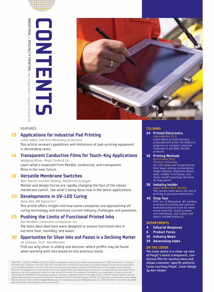
contentsindustrial + specialty printing M
arch/April 2012 • Volume 03/Issue 02
FEATURES
10 applications for industrial pad printingJulian Joffee, Pad Print Machinery of VermontThis article reviews capabilities and limitations of pad-printing equipment in demanding tasks.
14 transparent conductive Films for touch-Key applicationsWolfgang Milner, PolyIC GmbH & Co.Learn what’s expected from flexible, conductive, and transparent films in the near future.
18 Versatile Membrane switchesWim Zoomer and Neil Bolding, MacDermid AutotypeMarket and design forces are rapidly changing the face of the classic membrane switch. See what’s being done now in the latest applications.
22 developments in uV-led curingKarla Witt, INX Digital Int’lThis article offers insight into how some companies are approaching UV curing technology and examines current industry challenges and questions.
25 pushing the limits of Functional printed inksDon Banfield, Conductive Compounds, Inc.The tests described here were designed to assess functional inks in extreme heat, humidity, and water.
30 opportunities for silver inks and pastes in a declining MarketJill Simpson, Ph.D., NanoMarketsFind out why silver is sliding and discover where profits may be found when working with inks based on this precious metal.
coluMns34 printed electronics
Julia Goldstein, Ph.D.Learn about printed memory produced with either ferroelectric polymers or inorganic resistive materials in portable, flexible products.
36 printing MethodsRicha Anand, Ph.D., Phoseon TechnologyUV-LED lamps are recognized for their lower energy consumption, longer lifetime, improved robust-ness, smaller form factor, and faster on/off switching. But how do they work?
38 industry insiderJayna Sheats, Ph.D., TerePacThis column talks about the role of printing in pervasive electronics.
40 shop tourRSP, Inc. of Milwaukee, WI, handles a variety of printing and contract manufacturing services for mem-brane switches, touch screens, wire harnesses, and rubber and plastic molded products.
departMents4 editorial response6 product Focus32 industry news39 advertising index
on the coVerThe cover photo is a close-up view of PolyIC’s latest transparent, con-ductive film for touchscreens and shows customer-specific patterns. Cover courtesy PolyIC. Cover design by Keri Harper.

DOUTHITT
Contact us for more information on Douthitt’s complete line of Exposure Units, Vacuum Frames, CTS Imagers, Dryers, Inspection Tables, High Wattage UV Printing Lamps, Integrators and Blankets for any vacuum frame.
Visit us at www.douthittcorp.com
CONVENTIONAL OR CTS - DOUTHITT HAS THE OPTIMAL SOLUTION!
Contact us for a free catalog!
Once you’ve seen it you’ll never be satisfied until you own it
Model DMAModel Sahara Screen Dryer•Uniform Air and Heat to Insure Fast and Complete Drying of Screens•Stainless Steel Racks•Digital Temperature Control•Any Size Available
Model CTS Digital Screen Imager
The World’s Best Metal Halide Lamps
Olec Olite & Theimer Violux Lamps & Parts in Stock!
Model DMZ
THE DOUTHITT CORPORATION Call Toll Free 1-800-DOUTHIT(T) • www.douthittcorp.com
Phone 313-259-1565 Fax 313-259-6806 E-Mail [email protected]
Print head technology with smaller drop size and solid ink technology enables imaging halftone frequencies up to 75 lpi. Optimize image quality without compromising on throughput or consumable cost. Call us to see if CTS is right for you.
Douthitt’s self contained screen exposure systems provide the best vacuum contact and the best registration. Combined with our focused reflector metal halide printing lamps, our units offer the sharpest resolution, guaranteed coverage, shorter exposures and completely hardened emulsion.

4 | INDUSTRIAL + SPECIALTY PRINTING www.industrial-printing.net
transition from technology development to industrial manufacture. The company’s goal is to mass produce organic PV panels using vacuum-based, roll-to-roll, low-temperature processes. Männig said his company has set a record for cell ef ciency at 9.8% for a 1.1-cm2
tandem cell manufactured using a low-temp deposition process.
Jim Buntaine of Konarka talked about how his company spun out from the University of Massachusetts (Lowell) in 2001. He gave the history of PV, talking about how space power was needed in 1958 and that all satellites now use inorganic PV. From 1972 on, the energy crisis has motivated bringing PV to earth. In stage 3, from 1988, the global environmental impact of fossil fuel has begun to be recog-nized. The hope in phase 4 is for architectural power—PV power built into building materi-als. Konarka manufactures OPV cells using a roll-to-roll manufacturing technology and is capable of producing 250,000 ft2 (1 GW/year capability).
Zheng Xu of Solarmer Energy talked about driving down the cost of exible PV panels. Solarmer was founded in 2006, sprouting from technology licensed from UCLA and the University of Chicago. The company set world records for OPV ef ciencies. Xu said that the killer app is power-converting windows.
Solar still has a way to go in increasing ef ciencies, lowering costs, getting materi-als accepted as normal building supplies. Still, it feels good to know that the research from universities actu-ally results in practical jobs and real products for clean energy.
In President Obama’s State of the Union address in January 2012, he said that with America having only 2% of the world’s oil reserves, oil isn’t enough. And that “American oil production is the highest that it’s been in eight years.” At this rate, we have enough oil to last the U.S. 100 years. And then he promised that we would not walk away from the promise of clean energy. That’s a world-wide issue.
At FlexTech Alliance this year in Phoenix, AZ, iSP magazine headed a panel discussion on PV that presented many interesting ideas. Most of the panel members saw organic solar (OPV) as the wave of the future, because it uses organic (carbon-based) electronics for light absorption and charge transport. Be-cause the cells are made of plastic, they tend to be cheaper than silicon, and combined with the exibility of organic molecules and the possibility of additive printing technolo-gies for cell-material production, they are easier to make than silicon, thin- lm cells.
Many companies are involved in get-ting OPV from lab to fab. Bert Männig of Heliatek talked about how his company was spun off from the Technical University of Dresden and the University of Ulm in 2006, bringing together expertise in the elds of organic optoelectronics and organic oligomer synthesis. Right now, Heliatek is making the
Industrial + Specialty Printingwww.industrial-printing.net
STEVE DUCCILLI Group [email protected]
GREGORY SHARPLESS Associate [email protected]
GAIL FLOWER [email protected]
BEN P. ROSENFIELD Managing [email protected]
KERI HARPER Art [email protected]
LINDA VOLZ Production [email protected]
BUSINESS DEVELOPMENT MANAGERSteve [email protected]
EDITORIAL ADVISORY BOARDJoe Fjelstad, Brendan Florez, Dolf Kahle, Bruce Kahn, Ph.D., Rita Mohanty, Ph.D., Scott Moncrieff, Randall Sherman, Mike Young, Wim Zoomer
JERRY SWORMSTEDTChairman of the Board
TEDD SWORMSTEDTPresident
KARI FREUDENBERGERDirector of Online Media
CUSTOMER SERVICEIndustrial + Specialty Printing MagazineCustomer ServiceP.O. Box 1060Skokie, IL 60076
[email protected]: 847-763-9040
Energy for the FutureGAIL FLOWEREditor
EDITORIAL RESPONSE
Photo: (L-R) Gail Flower, editor, iSP; Stephen Bedell, Research Staff , IBM; Jim Buntaine, executive VP and CTO, Konarka; Zheng Xu, manager of device engineering, Solarmer Energy Inc.; Bert Männing, Co-founder, Heli-atek; Jean-Noel Poirier, VP sales, Global Solar Energy; Miles Barr, MIT.


| IndustrIal + specIalty prIntIng www.industrial-printing.net
electrically conductive adhesive Henkel Electronic Materials (www.henkel.com) recently developed a new, electrically conductive adhesive (ECA) compatible with lower-cost, tin-terminated components to enable more cost-effective as-sembly processes. ABLESTIK ICP-3535M1 is a one-component, pre-mixed ECA designed to provide low and stable contact resistance when used with 100% tin-terminated components. According to Henkel, the reliability of ABLESTIK ICP-3535M1 has been confirmed through various analyses, maintaining its stable contact resistance and good mechanical integrity after 3000 hr of temperature and hu-midity testing, 3000 cycles of thermal-shock evaluation, and 3000 hr of heat storage. Henkel says that, in each case, ABLESTIK ICP-3535M1 exhibits excellent performance with very small components, such as 0402s, displaying absolutely zero bridging or wicking with highly miniaturized devices.
product focusTh
e latest equipment and m
aterials for industrial printing
Flatbed UV Inkjet PrinterOcé (www.oceusa.com) recently announced the availability of the Océ Arizona 318 GL printer, a system the company describes as a highly capable, introductory flatbed UV inkjet printer that offers smaller print producers high-quality imaging. The system print at speeds up to 194 sq ft/hr (18 sq m/hr) or more than 20 2 x 3-ft (0.6 x 0.9-m) boards/hr. ONYX PosterShop X10 Océ Edition software is available to drive the printer. The Océ Arizona 318 GL can print on rigid media up to 49.2 in. (1250 mm) wide x 98.4 in. (2500 mm) long and up to 1.89 in. (48 mm) thick. Substrates are secured by a vacuum table, and the printer supports edge-to-edge printing, printing of multiple boards simul-taneously, registered double-sided prints, and the printing of large displays tiled over several boards. Océ’s White Ink Option enables under-printing for non-white media or objects, over-printing for backlit applications on transparent media, and printing white as a spot color. An option for roll-fed media is also available.

The right price.
From the benchtop to ourlargest unit, Xenon Sinteronsystems cost a fraction ofcompetitive solutions, whileoffering the features youneed.
The right company.
Xenon has pioneered the useof photonic curing in numerousindustries. Now we’re using ourexperience to revolutionizesintering for heat-sensitiveflexible circuits.
The right systems.
Need to sinter copper or silverink on flexible substrates?Choose from our family ofSinteron systems to matchyour research and develop-ment needs.
SINTERON 500
Linear Stage Unit
Scan this QR codewith your smart phoneto see the video.
See our videoThe Future of Flexible Printed Circuits Learn more about our low-
temperature sintering solutions atwww.xenoncorp.com/sinter
For the lab and beyond.
SINTERON 2000
9179-PrintElectAd_ISPmag.qxd:Layout 1 4/13/11 3:13 PM Page 1
Perfectly engineered for functional printing.
Disposable Medical Devices Printed Electronics Flexible Solar
Kammann K61-OS Roll to Roll Press
Flat Screen Head–offers the highest quality screen printing.
Servo Drives–superior tension control provides enhanced register capabilities.
Single Pass Production–reduces waste and increases production.
Roll-Fed Productivity Meets Flat Screen Quality
Flexible. Precise. Innovative.

| IndustrIal + specIalty prIntIng www.industrial-printing.net
SEND US YOUR PRODUCT NEWS Email [email protected]
Vacuum MotorsACI (www.aircontrolin-dustries.com) offers what it describes as an extensive range of vacuum pumps ideal for screen-printing ap-plications and
designed for easy retrofit. ACI units are driven by AC brushless motors and engineered for quiet operation. The brushless units are designed to ensure safe use in areas where solvents are present and low maintenance. ACI vacuum motors are multistage units of centrifugal design with impellers mounted directly on the motor shaft. The impellers are sheet aluminum and are balanced for optimum performance and minimal running stresses. They can be used for blowing and exhausting duties and support flow rates up to 500 cfm, pressures up to 64 in./SWG and 0.067-4 hp (0.05-3 kW). ACI’s vacuum motors conform to BS5000 Class B standard insulation and are C.S.A. approved.
Air-Filtration SystemPad Print Machinery of Vermont (ppmovt.com) has added a new air-filtration system to its line of auxiliary equipment. This system uses a combination HEPA and carbon tray for removal of fumes and gases with high particulate content. Clean Air
300 features include 300-cfm airflow, a filter-monitor gauge,
and swivel casters. The unit can connect to 2-, 2.5-, and 4-in.-diameter
(51-, 63.5-, and 102-mm) hoses.
Measurement Solutions
The N3 line of measurement solutions from Nanovea (www.nanovea.com) includes the M3, P3, and T3. The M3 is engineered to provide nanoindentation results under ASTM standards for use in R&D applications. Nanovea says its indentation method is fully automated with no need to observe the indent. The system features a touchscreen. The P3 is designed for 3D non-contact metrology and engineered to provide automatic nanometer ISO roughness and step data on nearly any material. The T3 is an auto-matic nano-wear tester using linear reciprocating, ASTM g133, for wear-rate study.
Double-Coated TapesPolyonics (www. polyonics.com) bills its double-coated tapes as ideal for bonding materials that will be exposed to extremely high temperatures and harsh manufacturing environments. They include liners that are designed to be die cut and to assist in auto-applica-tion. The double-coated tapes are designed to resist chemicals typi-cally found in PCB manufacturing, remain dimensionally stable at elevated temperatures, and provide excellent electrical properties, including dielectric strength. The double-coated polyimide tapes are offered in thicknesses of 1 and 2 mil and in high-temperature (up to 932°F, 500°C), ESD, and flame-retardant (tested for compli-ance with the UL94 VTM0 and FAR 25.853 flammability and BSS 7238/7239 smoke and toxicity standards) constructions.
Closed-Loop QA Solution
DEK (www.dek.com) calls its ProDEK an innovative and high-per-formance, closed-loop system tool designed to ensure print-perfor-mance optimization. It communicates between the DEK screen printer and solder-paste-inspection machine to identify any poten-tial problems and is engineered to maintain consistent, repeatable, high-quality output. Features include proactive defect prevention; process optimization without manual intervention; interfaces to Koh Young, Parmi, and Cyber Optics; ability to retrofit to all DEK printers powered by the standard Instinctiv V9 user interface; and more. ProDEK monitors a configurable quantity of printed circuit boards (PCBs), sending an independently corrected, forward and reverse offset to the printer, which then adjusts paste-on-pad alignment in real time. ProDEK uses barcode-based tracking tech-nology to ensure printed and inspected board synchronization.

march/april 2012 |
Films for Digital ImagingSihl Digital Imaging (www.sihlusa.com) has developed what it describes as an easy to print, easy to apply, and easy to remove clear film for use with aqueous inkjet printers. Sihl ClearSTICK-3166 is a 2-mil, clear, polyester film designed with and optically clear inkjet coating that Sihl says is ideal for interior application to virtually any substrate or surface. ClearSTICK-3166 is engi-neered for maximum inkload and fast drytimes with aqueous printers from HP, Epson, Canon, and others. Its white release liner allows for universal compatibility with media-feed and media-sensing systems. The film can be first- or second-surface printed. ClearSTICK-3166 is available in 75-ft (23-m) rolls and in widths of 17, 24, 36, and 50 in. (432, 610, 914, and 1270 mm).
Inkjet InkFujifilm (www.fujifilmusa.com) says its Color+ inkjet inks can help you achieve better color from your inkjet printer and make older printers run more efficiently. According to Fujifilm, Color+ inks are de-veloped to provide optimal performance on a wide variety of inkjet printers from most of the leading suppliers. The ink features Fujifilm’s MicroV fine-pigment-dispersion technology, engineered to reduce printhead clogging and offer stronger, brighter colors.
Ink for Seiko Printers3M Commercial Graphics (www.3m.com) and Seiko I Infotech Inc. (www.seiko-i.com) introduce GX 3M inks, billed as vibrant, flexible, colored inks made for use in Seiko I Infotech ColorPainter H Series printers and designed for printing onto many 3M brand opaque, translucent, and reflective graphics films. The solvent inks are formulated for excellent conform-ability and are available in eight colors (CMYKLcLm and two shades of W). Ac-cording to the companies, GX 3M inks are suitable for graphics applied to compound curves, corrugations, and riveted and flat surfaces and, when protected with the proper 3M overlaminate, are also durable and weather resistant.
Workflow SoftwareOnyx Graphics (www.onyxgfx.com) recently unveiled ONYX Thrive, a scalable print-production solution based on Adobe PDF Print Engine technology. ONYX Thrive software manages the workflow associated with wide-format-print produc-tion and is designed to offer print-service providers accurate, predictable, and high-quality results.
Onyx Thrive workflow software is powered by Adobe technologies, including the Adobe PDF Print Engine, a rendering-engine technology that Adobe partners use to build tailored solutions for their market segments. Onyx’s software features the Thrive Production Manager, a browser-based user interface that enables print-service providers to submit, control, and monitor jobs and devices from a Mac, PC, or mobile device.

10 | INDUSTRIAL + SPECIALTY PRINTING www.industrial-printing.net
FEATURE STORY
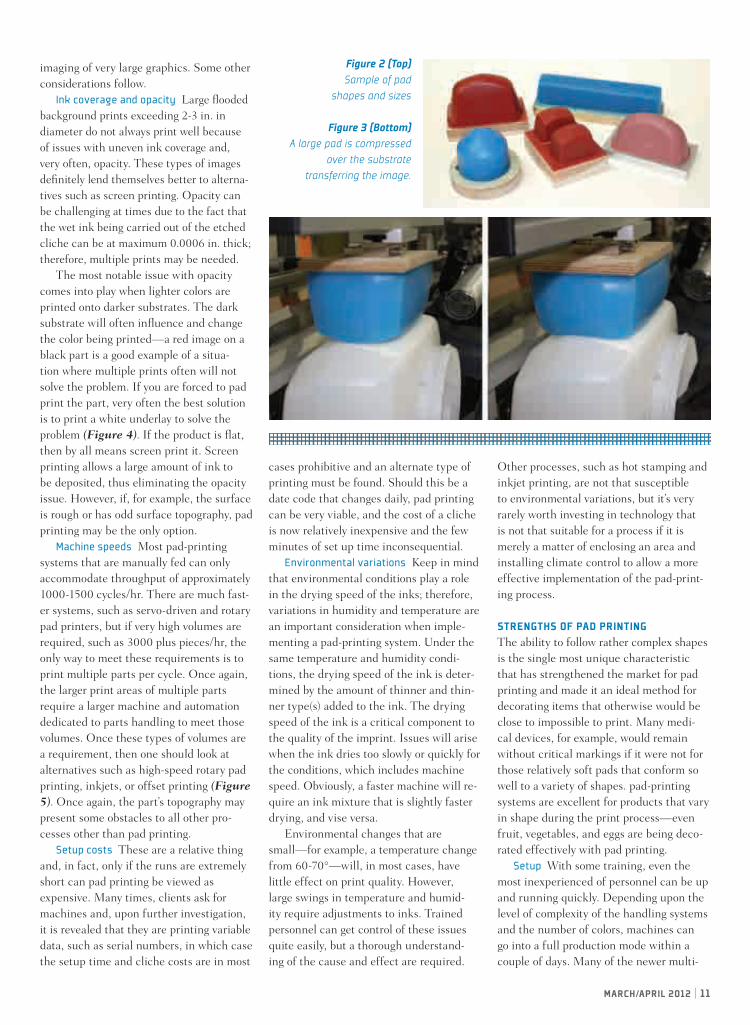
When many of us think of pad printing, we automatically picture printing onto complex, three-dimensional products such as golf balls or medical devices (Figure 1). The reality is that certain products lend themselves well to pad printing while others do not; many others can be deco-rated with multiple different processes. The single most differentiating functional component of the pad-printing process is the silicone printing pad (Figure 2) and its unique characteristics.
Its function is to transport the im-age from the etched cliche (plate) to the substrate being printed. Pad shapes, sizes, and durometer can be modi ed to suit the characteristics of the object being printed, but they also must comply with the laws of pad printing. That statement brings me to an observation: Many times, a client has asked why the pad shape cannot be at or even concave. The answer is to pick up the image effectively, it must roll onto the cliche to allow the exclusion of air between the ink in the etched image area on the cliche and the pad surface (Figure 3).
As a general rule, the harder a pad, the larger the radius can become. A very rm pad can have a less pointed shape than a
very soft pad. Another generality is that a harder pad prints a crisper image than a soft pad. Very rm pads tend to force ink to move within the etched areas and can cause problems that look like ghosting, particularly when larger ink surfaces are being printed/transferred. Very soft pads, in some cases, will not transfer or pick up an image in its entirety, leading to rough edges or voids.
LIMITATIONS OF PAD PRINTINGWhile fairly large images can be printed, the cost of a machine for printing an image 8 in. in diameter in one color can approach $50,000. Large images require large pads, which in turn require large machines and, with them, a high price. In general, pad printing is highly suited to smaller images, but there are many exceptions involving highly successful
APPLICATIONS FOR INDUSTRIAL PAD PRINTING
Figure 1 Variety of products where pad printing was used
Julian Joff ePad Print Machinery of Vermont
e initial investment in pad printing can be high, but read on to discover the process’s many
economies in industrial imaging.
march/april 2012 | 11
imaging of very large graphics. Some other considerations follow.
Ink coverage and opacity Large flooded background prints exceeding 2-3 in. in diameter do not always print well because of issues with uneven ink coverage and, very often, opacity. These types of images definitely lend themselves better to alterna-tives such as screen printing. Opacity can be challenging at times due to the fact that the wet ink being carried out of the etched cliche can be at maximum 0.0006 in. thick; therefore, multiple prints may be needed.
The most notable issue with opacity comes into play when lighter colors are printed onto darker substrates. The dark substrate will often influence and change the color being printed—a red image on a black part is a good example of a situa-tion where multiple prints often will not solve the problem. If you are forced to pad print the part, very often the best solution is to print a white underlay to solve the problem (Figure 4). If the product is flat, then by all means screen print it. Screen printing allows a large amount of ink to be deposited, thus eliminating the opacity issue. However, if, for example, the surface is rough or has odd surface topography, pad printing may be the only option.
Machine speeds Most pad-printing systems that are manually fed can only accommodate throughput of approximately 1000-1500 cycles/hr. There are much fast-er systems, such as servo-driven and rotary pad printers, but if very high volumes are required, such as 3000 plus pieces/hr, the only way to meet these requirements is to print multiple parts per cycle. Once again, the larger print areas of multiple parts require a larger machine and automation dedicated to parts handling to meet those volumes. Once these types of volumes are a requirement, then one should look at alternatives such as high-speed rotary pad printing, inkjets, or offset printing (Figure 5). Once again, the part’s topography may present some obstacles to all other pro-cesses other than pad printing.
Setup costs These are a relative thing and, in fact, only if the runs are extremely short can pad printing be viewed as expensive. Many times, clients ask for machines and, upon further investigation, it is revealed that they are printing variable data, such as serial numbers, in which case the setup time and cliche costs are in most
cases prohibitive and an alternate type of printing must be found. Should this be a date code that changes daily, pad printing can be very viable, and the cost of a cliche is now relatively inexpensive and the few minutes of set up time inconsequential.
Environmental variations Keep in mind that environmental conditions play a role in the drying speed of the inks; therefore, variations in humidity and temperature are an important consideration when imple-menting a pad-printing system. Under the same temperature and humidity condi-tions, the drying speed of the ink is deter-mined by the amount of thinner and thin-ner type(s) added to the ink. The drying speed of the ink is a critical component to the quality of the imprint. Issues will arise when the ink dries too slowly or quickly for the conditions, which includes machine speed. Obviously, a faster machine will re-quire an ink mixture that is slightly faster drying, and vise versa.
Environmental changes that are small—for example, a temperature change from 60-70°—will, in most cases, have little effect on print quality. However, large swings in temperature and humid-ity require adjustments to inks. Trained personnel can get control of these issues quite easily, but a thorough understand-ing of the cause and effect are required.
Other processes, such as hot stamping and inkjet printing, are not that susceptible to environmental variations, but it’s very rarely worth investing in technology that is not that suitable for a process if it is merely a matter of enclosing an area and installing climate control to allow a more effective implementation of the pad-print-ing process.
StrengthS of pad printingThe ability to follow rather complex shapes is the single most unique characteristic that has strengthened the market for pad printing and made it an ideal method for decorating items that otherwise would be close to impossible to print. Many medi-cal devices, for example, would remain without critical markings if it were not for those relatively soft pads that conform so well to a variety of shapes. pad-printing systems are excellent for products that vary in shape during the print process—even fruit, vegetables, and eggs are being deco-rated effectively with pad printing.
Setup With some training, even the most inexperienced of personnel can be up and running quickly. Depending upon the level of complexity of the handling systems and the number of colors, machines can go into a full production mode within a couple of days. Many of the newer multi-
Figure 2 (Top) Sample of pad
shapes and sizes
Figure 3 (Bottom) A large pad is compressed
over the substrate transferring the image.

12 | IndustrIal + specIalty prIntIng www.industrial-printing.net
color systems have servo controls for image placement and can be set up with ease and speed.
Many manufacturers fail to implement a prepress system that allows for very quick changeovers. The process may take a few extra minutes in the graphics department and in the platemaking process, but it can save hours per day in the print room. Prereg-istered artwork and positives with punch tabs are the well kept secret that many manufacturers and contract printers fail to note. Today, with new plate lasers being used, there is no excuse for not registering etchings on the cliches so the artwork is always in the correct position when changeovers take place.
Autonomy through simplicity Ease of setup and platemaking allows small companies to create artwork and, in turn, make the cliches in house so that they can offer quick turnaround to cus-tomers. The advantages here are huge as the just-in-time mentality of many industries always views this capability as an essential part of doing business with chosen suppliers.
The only other print process that is even simpler is inkjet, where direct-to-print comes to mind. The advent of the laser has further simplified the cliché-making process, and time to market can be reduced even further when you are prepared for the relatively high cost of entry to laser-based platemaking (Figure 6). One of the biggest advantages of pad printing is the fact that you could get a call in the morning and have a sample out to your customer that same day.
Figure 4 (Top)White ink pad printed on a black irregular surfaceFigure 5 (Below)Rotary pad printerpad printing equipment
and supply Manufacturers and distributors
all aMerIcan Mfg. & supplyscreenprintsupply.com
cosMex graphIcs Inc.cosmexgraphics.com
dIversIfIed prIntIng technIques Inc.diverprint.com
ever BrIght prIntIng MachIne pty ltd.everbrightprinting.en.alibaba.com
Inkcups nowinkcups.com
Itw trans techitwtranstech.com
MIcrotec technology co. ltdszmicrotec.com
pad prInt MachInery of verMontpadprintmachinery.com
peMIagaan haI kuang sdn Bhdhaikuang.com
pentex prInt Master IndustrIesinkflexx.com
prInta systeMs
printa.com
reIsch & assocIatesreischpad.com
serIgraf ltd.serigraf.ie

Figure 6 Rapid fi re laser etcher and plate etched within the laser
Costs associated with set up The relatively low cost of cliches and inks allows the cost of production to remain low. Pad-printed labels commonly cost manufacturers tenths of a cent in larger pro-duction environments, making the return on investment way shorter than industry standards. However, fast ROI is not always the case, and some of the larger, more automated, systems will often have ROI numbers getting into the range of 18-24 months. There is no need for highly skilled personnel to set up equipment, thereby help-ing to keep production costs down (Figure 7).
Low VOCs Closed-system pad printing is a process that, under normal conditions, does not require the use of extreme venting. You still should use air-carbon- ltration safety though. In most cases, due to the enclosed nature and structure of the pad-printing equip-ment, one air ltration unit can easily cover at least three machines. Pad printing almost always uses a solvent-based ink and of the sol-vent-based systems on the market, it is by far the easiest to control in terms of VOCs. I recall the complaints of one customer; and when I walked in to investigate the smell problem, I found that they had left solvent-soaked rags in open garbage cans in the production area. Once we exchanged them for sealed cans, the problem vanished.
After 25 years in this business, I still feel pad printing is the most exible and versatile decorating solution for many dif cult-to-mark applications. The initial investment in a pad printer can be high, but compared to other forms of product decorating—such as labeling garment tags using hot stamping and screen printing—pad printing cost per item is very economical. Pad-printing technology is continually evolving and more manufacturers are using pad printers within their production lines or adding automation to basic printers to reduce labor costs.
There are always multiple ways to achieve the same objective. The key to success is selecting one that is the simplest, most exible, cost effective, and will grow with your company. One last thing, nd a supplier that knows the process and can and will service the systems they supply.
Julian Joff e, founder and CEO of Pad Print Machinery of Vermont started his fi rst company in the textile manufacturing fi eld in Yonkers, NY. Joff e’s interest in engineering and his desire to help people has built the company into a 25,000-square-foot facility in East Dorset, Vermont. e company employs high-tech engineers designing and building industrial inkjet print-ers and automated pad-printing systems.
JULIAN JOFFEPad Print Machinery of Vermont
Get the best information…whenever you want it.
Receive monthly print editions ofIndustrial + Specialty Printing magazine
Receive the weekly E-newsletter
Search industrial-printing.net anytime
•
•
•
Visit industrial-printing.net/subscribe to start your subscription today.
Already a subscriber to iSP? Lock in your subscription by visiting industrial-printing.net/renew
MARCH/APRIL 2012 | 13
January/february 2012www.industrial-printing.net
Inkjets in Electronics Applications
Printing Processes For Photovoltaics
The Future of Functional Printing
Materials and Methods for Printed OLeDsP. 20
The Future of Functional Printing
News & Trends Products Message Boards Calendar Newsletter Sign-Up Bookstore
INDUSTRY UPDATE PRODUCTS & TECHNOLOGY
TECHNIQUES, TIPS & APPLICATIONS
Top Stories • Printing Photovoltaics Screen printing photovoltaic cells
is the most reliable method and fastest growing application in industrial printing.
• Automating Your Pad-Printing Operation
Automation is an important part of effi cient, consistent pad printing. Find out about some of the options designed to enhance speed and precision for industrial applications.
• Membrane Switch: Screen Printing 101
The membrane-switch market has experienced dramatic growth and soared to an unprecedented level.
• Industry InsiderThe Importance of Printed Electronics to P&G
Textured Polyester Film >> Autotex S (Steel) is a textured
polyester fi lm from MacDermid Autotype(www.macdermidautotype.com) that’s designed to replicate a stainless-steel fi nish for.
Automotive printing >>
Conductive inks >>
Decals / nameplates >>
Finishing and QC >>
Hot stamping >>
In-mold decorating >>
Inkjet printing >>
Lighting OLED >>
Management >>
Medical devices >>
Membrane switches >>
Pad printing >>
Photovoltaics >>
Printed electronics >>
SPOTLIGHT
username password Log in
March/april 2010
www.industrial-printing.net
Extending Printing
Capabilities
Membrane Switches 101
Growing a Label Business
printingphotovoltaicsP. 22
SubscribeToday
Printing equipment used in manufacturing
NEW:Industrial + Specialty PrintingMAGAZINE

14 | INDUSTRIAL + SPECIALTY PRINTING www.industrial-printing.net
COVER STORY
Wolfgang MildnerPolyIC GmbH & Co.
Learn how specialized fi lms will transform the way myriad printed-electronics products are manufactured.
TRANSPARENT, CONDUCTIVE FILMS
FOR TOUCH-KEY APPLICATIONS
Poly TC transparent
conductive fi lm

MARCH/APRIL 2012 | 15
The form-follows-function design is all-important for modern car cockpits, cell phones, and electronic equipment in general. Purely functional design represents a thing of the past, while look and feel have become crucial selling points. Transparent, conductive lms enable new design possibilities to be created—designs for controls and touch keys that are integrated into transparent sur-faces or transparent touch keys on curved surfaces.
Will you be able to control your car radio using buttons located directly on the dashboard in the future? Will we be able to move transparent side windows just by touching them? Will the controls on the center console be transparent touch keys instead of me-chanical buttons? Will the hands-free keypad only appear when a driver wants to make a call and be invisible on the dashboard the rest of the time?
These are visions of the future that will, for example, make car-interior designs even more attractive. However, transparent, conductive lms are necessary for the implementation of such integrated controls. At present, these displays are manufactured using lm that is coated with indium tin oxide (ITO), the most common material used for this purpose. As well as being transpar-ent, these lms also conduct electric current. ITO offers limited freedom of design; however, due to its restricted conductivity, rela-tive fragility, and the complexity of the structuring process, it may not be used as often in future transparent, conductive lms.
FILMS FOR FUTURE CELL PHONESAnd what is in store for the future of the cell phone? What will follow smartphones? Cell phones are becoming ever lighter and slimmer. Using transparent and conductive lms, their shapes could become more ergonomic and devices could be considerably more exible to make using them user-friendly.
Alternatives to ITO are now available that compensate for its disadvantages. One option, based on printed-electronics-plat-form technology, is a type of cost-effective, exible, electronic product that can be produced in high volumes. These lms are considerably exible, transparent, and thin (Figure 1). They can either be used as a surface or be incorporated behind plastic, glass, and many other materials.
PRINTED ELECTRONICSPrinted electronics generally refers to electronic components or assemblies that are manufactured or partially manufactured using printing methods. These processes use electronic conducting and semiconducting functional materials instead of just graphics inks. Semiconducting materials are usually based on specialized plas-tics. Modern, high-volume, roll-to-roll printing methods reduce the cost of manufacturing and duration of production. In this way, they open new elds of application to which conventional (inor-ganic) electronics have hitherto had limited or no access. Thanks to printed electronics, new developments are emerging in large-scale applications such as RFID tags, displays and solar cells.
High production speed and the possibility of producing very large quantities using rapid, roll-to-roll processes are the starting point for printed electronics. Several layers of different materi-
als are laid on top of one another with great precision to create a continuous roll. This allows rms to manufacture functional lms, such as electronic circuitry, that include all components (transistors, capacitors, diodes, etc.) using printed electronics. The production of electrode structures plays a major role and is the cornerstone of the process. It enables high-resolution, narrow conductor tracks to be produced on a large scale. The production of high-resolution structures at micron scale on thin, exible, PET lms can achieve both adequate conductivity and transparency of layers (Figure 2).
TRANSPARENT, CONDUCTIVE FILMS Electrode-structure production can generally be used for any high-resolution structure on polyester lm. The structure of the conductor tracks is so ne that the opaque metal can no longer be detected by the human eye and appears transparent. The conduc-tor tracks are not created as wide lines on the lm, but as a very ne conducting grid. The lm is produced using a special roll-to-roll printing process, a type of production that has its origins in printed electronics. This process allows large quantities to be produced and guarantees the exibility of the lm. Film structure and dimension can be adjusted to the particular eld of applica-tion and to suit customers’ requirements.
Companies market these exible, conductive, and transparent lms. That can be used in a diverse range of applications. Today, the touchscreen market is growing rapidly. Current conventional touch displays use lms that are coated with ITO; however, ITO lms are becoming more and more expensive due to the scarcity of indium, a rare metal. For this reason, manufacturers are look-ing for adequate alternatives to this type of lm that can be used in a variety of touch applications, including screens and keys.
Other elds of application can also be addressed. Transpar-ent, conductive lms could conceivably be used as a transparent, EMI-shielding lm to block electromagnetic waves, as transparent heating lms, or as electrodes.
Transparent PET Substrate
Gap Width
Conductive Area
Pads & Wiring
Example for Individual Layout
Figure 1 High Resolution Image
200µm
Example for a microscopic picture of conductive layer
16 | IndustrIal + specIalty prIntIng www.industrial-printing.net
transparent fIlms for touchscreensWhat are resistive and capacitive touchscreens? Touch sensors differ with regard to their respective application in touch keys and touchscreens. They are the basis of modern, interactive input devices that have the advantage of being incredibly easy to use. Touchscreens are touch-sensitive surfaces. A distinction is made between capacitive and resistive touch.
Resistive touch sensors use the pressure an object exerts on an input medium to establish a connection between two transpar-ent conducting layers. The exact XY position of a touch point on a surface can be calculated from this electrical contact using the voltage gradients applied on the films in the X and Y directions.
Capacitive touch sensors already recognize the proximity of electrically conducting objects, but can be regulated so that they have to be touched to react. In contrast to resistive technology, pressure is not required. The surfaces of capacitive touch sensors are electrically charged. When touched with a finger, a small transfer of charge is created. This small current can be measured on the surface where the uniform electrical field is established. Variations in its intensity in comparison to the areas that have not been touched allow the specific touch point to be precisely traced. Capacitive touch enables the use of applications that can detect the touch of one or more fingers on contact sites across the entire surface. Appropriate gestures made with one or more fingers can be recognized (multi-touch capability).
Resistive touch sensors have set the touchscreen boom in motion; this process was additionally boosted by the multi-touch capability of capacitive sensors, a trend that is still going strong. Currently, for example, smartphones with multi-touch functional-ity are equipped with capacitive sensors.
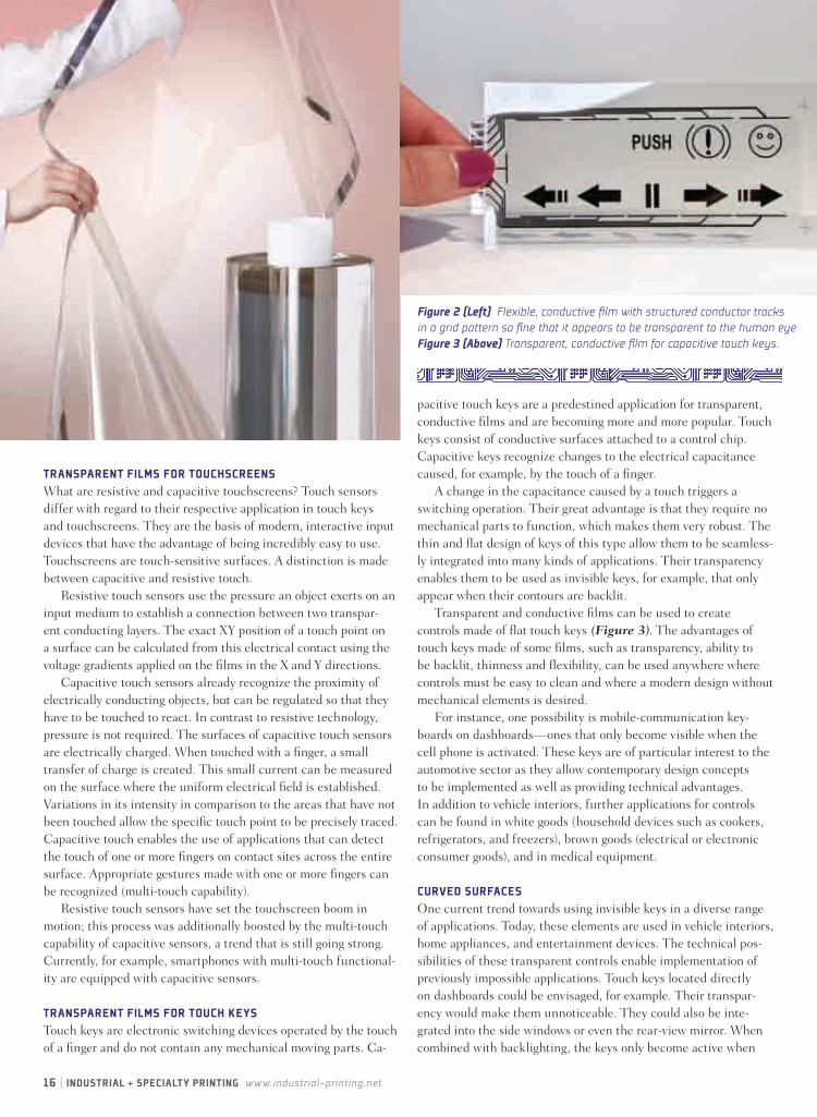
transparent fIlms for touch keysTouch keys are electronic switching devices operated by the touch of a finger and do not contain any mechanical moving parts. Ca-
pacitive touch keys are a predestined application for transparent, conductive films and are becoming more and more popular. Touch keys consist of conductive surfaces attached to a control chip. Capacitive keys recognize changes to the electrical capacitance caused, for example, by the touch of a finger.
A change in the capacitance caused by a touch triggers a switching operation. Their great advantage is that they require no mechanical parts to function, which makes them very robust. The thin and flat design of keys of this type allow them to be seamless-ly integrated into many kinds of applications. Their transparency enables them to be used as invisible keys, for example, that only appear when their contours are backlit.
Transparent and conductive films can be used to create controls made of flat touch keys (Figure 3). The advantages of touch keys made of some films, such as transparency, ability to be backlit, thinness and flexibility, can be used anywhere where controls must be easy to clean and where a modern design without mechanical elements is desired.
For instance, one possibility is mobile-communication key-boards on dashboards—ones that only become visible when the cell phone is activated. These keys are of particular interest to the automotive sector as they allow contemporary design concepts to be implemented as well as providing technical advantages. In addition to vehicle interiors, further applications for controls can be found in white goods (household devices such as cookers, refrigerators, and freezers), brown goods (electrical or electronic consumer goods), and in medical equipment.
curved surfacesOne current trend towards using invisible keys in a diverse range of applications. Today, these elements are used in vehicle interiors, home appliances, and entertainment devices. The technical pos-sibilities of these transparent controls enable implementation of previously impossible applications. Touch keys located directly on dashboards could be envisaged, for example. Their transpar-ency would make them unnoticeable. They could also be inte-grated into the side windows or even the rear-view mirror. When combined with backlighting, the keys only become active when
Figure 2 (Left) Flexible, conductive film with structured conductor tracks in a grid pattern so fine that it appears to be transparent to the human eyeFigure 3 (Above) Transparent, conductive film for capacitive touch keys.

march/april 2012 | 17
required and are invisible the rest of the time. In addition to their high transparency and conductivity, the
great flexibility of the films is a further advantage. Previously, transparent touch keys had the restriction that they could only be integrated into flat surfaces. Flexible controls, however, can now be built into surfaces that are curved or uneven (Figure 4). Touch keys can actually be positioned anywhere on the dynamic contours of a dashboard or center console. These new technolo-gies open up unprecedented opportunities for creative design in vehicle interiors.
In addition to their use in touch keys, transparent, conductive films can be used to implement further touch applications. Their ability to be structured in any desired form enables extensive grid structures to be created. This kind of transparent grid structure can be used to make larger touch applications, such as touch-sen-sitive screens. Resistive or capacitive single-touch or multi-touch applications of the kind used today in touch monitors and smart-phones can be manufactured by combining two films.
Touch sensors are becoming ever more popular as replacements for mechanical buttons and controls. The new trend is already clear: capacitive buttons and controls with attractive graphic designs integrated into surfaces. Attractive graphic surfaces are be-coming increasingly important for equipment and controls particu-larly in the electronics, mobile communication and automotive sec-tors. Outstanding results can be achieved by combining transparent and conductive films with IMD (in-mold decoration) films. In this way, the surface in question is no longer disrupted by mechanical keys as the keys can be integrated behind the decoration.
Non-conductive, metal IMD films can even be used to manu-facture metallic surfaces and create, for example, brushed-metal-effect surfaces with integrated controls. The combination of touch sensors and IMD hints at the wealth of possibilities that can be achieved through the fusion of flexible design and application tech-nologies, such as IMD, with the functional/electronic world. Prod-uct designers have been given a new dimension of creative freedom that is less and less restricted by conventional electronic standards and with graphic elements playing a more significant role.
Further scope For transparent, conductive FilmsElectrodes are electrical conductors, usually of metal, that are used to conduct electricity. Some film can be custom-printed with a conductive structure. It is even possible to print the conductors so finely that they become invisible to the human eye and enable transparent electrode grids to be manufactured. It is thus of particular use in applications requiring invisible current transport. Unlike other transparent conductors, such as ITO, the printed grid structures are a neutral shade so colors are not distorted. This opens up a multitude of application options for this type of film, including organic light-emitting diodes (OLED), organic solar cells (OPV), printed transistors, or as heating electrodes for
screens and mirrors.Further uses for electrodes Conductive structures can also
be useful in any application that converts energy into heat. The extreme fineness of the conductive structures and layers places natural limitations on the heating elements. There are interesting perspectives for local heating elements—for example, to prevent windscreens and mirrors from misting up. The amount of energy required is so small that the structures necessary to transport it cause no optical impairment.
Electrodes for EMC shielding The term EMC (electromagnet-ic compatibility) refers to electronic interference that can disturb electronic devices or even be produced by them. The increasing complexity of electronic circuits—for instance, in the automotive sector—has also caused an increase in disturbances triggered by electromagnetic waves. This risk can be curbed by using com-ponents that come under the category of EMC shielding. Some transparent, conductive films provide the following advantages for EMC shielding:
• Customer-specific layouts, including grids in rhombic, rect-angular, or hexagonal designs
• Individual adjustment of the surface resistance and, there-fore, the shielding effect and desired transparency
• Customer-specific geometry can be used to set the EMC film cut-off frequency as desired
conclusionPrinted electronics—the production of electronic components and products based on roll-to-roll processes—have left the laboratory and are displaying the first successful applications in the mass market. Products of this type pave the way for a whole spectrum of practical, large-scale applications They provide clear advantages with regards to both product design and integration into target applications. Finished products have become more economically priced for consumers.
Flexibility and high conductivity in conductive films enable innovative touch keys to be manufactured that improve the look and function of modern vehicle interiors. Curved or transparent surfaces are no longer an obstacle for these thin films. Function follows design.
Figure 4 It will be possible to dispense with conventional buttons and keys completely in the future. Flexible and conductive films can also be mounted on curved surfaces behind the dashboard.
Wolfgang Mildner is managing director of PolyIC GmbH & Co. KG in Fürth, Germany. He studied computer science at the Technical University of Erlangen. He is member of the Board of the Organic Electronics Association/VDMA and the German Flat Panel Foundation (DFF). For more information, visit polyic.com.
WolFgang mildnerOrganic Electronics Association

18 | IndustrIal + specIalty prIntIng www.industrial-printing.net
A membrane touch switch is a thin, integrated, front-panel assembly that has at least one flexible layer (Figure 1). The assembly typically comprises several layers of screen-printed polyester layers, spacers, polymer thick-film (silver) circuits, adhesive layers, and often a rigid backer. Often the whole assembly is incorporated into a metal or engineered plastic box to complete the control panel.
Membrane touch switches have been used in electronics applications for almost 50 years. Since their introduction, mem-brane touch switches have evolved to become sophisticated, and often highly com-plex, electronic components. They are used in a broad spectrum of products, including industrial controllers, test equipment, criti-cal medical devices, consumer appliances, and toys.
Today, a membrane touch switch can feature multiple circuit layers, integrated display windows, embedded devices such as LED displays, high-definition graphics and even touch screen technologies. The chal-lenge is to maintain consistency and quality while incorporating the latest materials and production processes to meet customer demands. Let’s take a quick look at the key components before looking at examples of the latest designs of some membrane switches.
componentsThe graphic overlay is the top layer of the
membrane touch switch. It connects the operator to the device. Historically, the graphics are screen printed onto the second surface of the top layer. The material of choice has overwhelmingly become an en-gineered polyester film. The films typically range from a thickness of 0.005 to 0.010 in.
Polyester, which is bi-axially oriented polyethylene terephthalate (PET), was introduced as a more durable alternative to polycarbonate. Polycarbonate was widely used for control panels, but now it tends to be used sparingly and primarily in applica-tions with requirements for low actuations. Polyester keypads can be actuated more than three million times before showing any kind of wear.
At present, digital printing is an option used to decorate the switch. Screen printing works well when larger volumes are required or high-performance, functional graphics are needed. Prototypes or small volumes may be printed using a digital printing technique. The primary advantage of digital printing is that an unlimited quantity of unique graphic overlays can be printed using this equipment. The specialty coating of the overlay and its thickness protects the graphics and circuitry from the environment and enables the operator to ensure visual appeal, haptic/tactile, response, and overall durability.
The electrical circuits are primarily screen printed onto specialty heat-stabilized polyester film. By far the most commonly
used conductor is silver in the form of a conductive polymer thick-film (PTF) ink. Carbon-based inks are also used sometimes to give added protection to the silver when the switch is used in an extreme environ-mental condition.
Membrane switches can be either tactile or non-tactile. Because operators of equip-ment often require feedback when pressing a key, domes can be assembled as a part of the membrane, to provide a tactile feedback and a positive snap-action response. Tactile membrane switches typically incorporate a metal dome embedded in the membrane switch. Alternative options are for polyester domes that are formed in the circuit or in the graphic-overlay layer. The dome’s size and material make up, in conjunction with the overlay, controls the actuation force and tactile response. Metal domes are avail-able in a wide range of shapes and sizes. Different polyester-dome-actuation forces can be achieved by modifying the height and the diameter of the dome. Non-tactile membrane switches produces a low actua-tion force, determined by the circuit spacer thickness.
Spacer layers and adhesive layers are used to separate the circuit layers (Figure 2) and to provide key openings to allow con-tacts for conductors and bind all the layers together to form a complete unit.
Displays and backlighting are supplied predominantly by liquid-crystal displays (LCDs) and by relatively low-cost light-
feature story
Versatile MeMbrAne SwitcheS
Learn about the latest materials and methods for
membrane-switch production. Neil Bolding and Wim Zoomer

march/april 2012 | 19
emitting diodes (LEDs) when selective backlighting is required. Embossing is often required to provide a raised feature to em-bed surface-mount LEDs. Other options are fiber optics and electroluminescent lighting (EL). EL uses an indium-tin-oxide-coated (ITO) film, or a conductive polymer. The active light-emitting layer is a phosphorous or zinc-oxide printed layer to backlight the keypad, followed by a dielectric printed layer that separates the silver conductive ink printed rear electrode.
meeting the challengesAfter the recent downturns in the global economic climate, the manufacturer is being challenged to produce high-quality parts with fewer resources and reduced margins. The use of digital technologies is increas-ing; it is on the rise to produce prototypes and small production runs at the cost of traditional analog processes. They can do so at a reduced cost and often with an improved lead time. The issue at hand is the ability to provide the same performance levels of the analog process. To date this has not been readily achieved. The latest switch designs incorporating additional functionality will be reviewed to show the developments in the membrane switch industry and highlight the next generation of functional switches that are coming from established companies.
To provide effective use over long service lives, membrane touch switches must be designed and manufactured carefully with
The sector for stylus-controlled devices is expanding. The outer film requirements are becoming more demanding, while the touch and visual appearance is critical. High impact resistance, combined with excellent optical clarity, is required. Bristol, UK-based Clue Trader Ltd, part of the BOM Group (Figure 4), and a software and hardware developer of IT systems for airlines, retail-ers, and government bodies, has developed a line of screen protectors using hardcoated polyester. The challenge was to find a solu-tion that would offer additional protection to each TFT display without affecting its definition or tactile response.
Kienzle Systems of Germany has de-veloped the latest generation of heavy-duty tablet PCs (Figure 5) for extreme outdoor use with protection from vibration and water spray in areas such as land registry and surveying assignments, outdoor mapping, industrial and construction sites, and even rescue operations. High levels of UV light in such environments affects the performance of conventional membrane key pads, caus-ing discoloration and embrittlement of the surface layers.
Switches often must resist harsh chemical conditions and cleaning regimes as required in hospitals or commercial kitchens, or within an industrial workplace where aggressive solvents and cleaners may be used. The film substrate used to form the outer layer of the switch or keypad is criti-cal to the product’s longevity. Therefore,
Figure 3 Membrane switches used in a marine environment must be functional in adverse conditions. Photo courtesy of Electronic Imaging, NZ.
the conditions in mind and constructed from specialized materials to make them resistant to extreme mechanical or environ-mental stress. Membrane touch switches are routinely used in extreme conditions, such as high-temperature and high-humidity environments when used as spa (hot-tub) controllers or exposed to high heat and sun (UV irradiation) when used as oil-pumping switches or as sophisticated control panels in a marine environment (Figure 3) when exposed to tropical weather conditions.
Other controllers may be found in potentially hazardous environments with a risk of explosion and high levels of dust and dirt, such as in mining. They are developed to withstand extremely harsh operating conditions with high levels of abrasive wear, high-pressure wash-down, and, in many applications, shock waves from coal-face blasting. The operator panels are essential components in the overall system. They pro-vide control of specific functions at the coal face and local visual feedback of system sta-tus. Each panel is constructed from a robust stainless steel enclosure into which beveled LCD-display windows and membrane-key apertures are machined.
The individual membrane keys provide a high degree of tactile response for operators wearing heavy-duty gloves. The membrane keys are protected by a single layer 0.006-in.-thick hardcoated film, mounted and sealed directly beneath the open display windows and key apertures.
Figure 2 Spacer and adhesive layers are used to separate circuit layers and to provide key contact openings for conductors in this circuit and backer.
Figure 1 This membrane touch switch is an integrated, thin, assembly with at least one flexible layer.

20 | IndustrIal + specIalty prIntIng www.industrial-printing.net
it is important that membrane-keyboard manufacturers select the right film for each application. The latest generation of film substrates has been developed to provide manufacturers with a wide choice of film properties that can best be matched to their needs.
Other applications dictate additional functionality, such as cleanliness require-ments in a medical or hospital environment. To this extent, anti-microbial agents are available for use, and have been incorpo-rated into film coatings. For example, anti-microbial overlay panels provide protection in a range of medical-gas area alarms. These alarms are used in hospitals to monitor the supply and condition of vital medical gasses. The hardcoated film incorporates a specially developed anti-microbial agent, ensuring that the microbial properties persist for the lifetime of the film. In addition, the film provides a scratch- and chemical-resistant surface that can withstand everyday rigors and the most aggressive cleaning methods.
aesthetIcsThere is not just a need for functionality, but also a high degree of image aesthet-ics and feel to functional switches today. The aesthetics can be incorporated by the graphic image, the overlay film itself, and the functionality through design. In today’s challenging economic climate, businesses are developing new technologies and pro-duction methods to distinguish themselves from the competition and meet ever complex consumer demands. This is especially true of the design and manufacture of high-quality electronics, such as membrane switches and keyboards and fascia panels. These applications now offer as standard a wide range of sophisticated functions, with multiple circuit layers, tactile keys, and integrated displays.
In particular, increasing focus has been placed on the aesthetic qualities of these electronic components as the demand for highly stylized parts continues to grow. Bex Design Services has pioneered the use of a combination of screen and digital printing with the use of flexible mirror inks and a specialty film designed to exhibit a stainless-steel finish at far lower costs than traditional metal overlays. This technology capitalizes on the high-definition capa-bilities of digital printing to manufacture multi-colored, reverse-printed, fine-line text and graphics. The digital print is overprinted using conventional screen techniques with the latest flexible mirror inks to complete the stainless-steel effect. A black print is finally added to give ad-ditional depth to the color to enhance the overall effect.
Butler Technologies sees an opportunity within the emerging concept of graphics and printed circuitry being combined into a single, formed part. One such method to accomplish this is printing both decorative and functional inks onto the same formable polycarbonate film. The printed film is then thermoformed to shape, trimmed to size, and inserted into a plastic injection mold, where resin is shot behind the printed film. The result is a three-dimensional, fully functional part with conductive circuitry and the necessary in-molded connectors and mounting hardware. Examples of this are capacitive-touch user interfaces in the automotive and appliance industries.
Butler Technologies also sees growth in the integration of silicone-rubber keypads and capacitive-touch technology into membrane-switch applications, as well as the change to digitally printed graphics to add appeal. This has forced them to learn and integrate new technologies and design capabilities.
Figure 4 (Left) High impact resistance and excellent clarity are required for outer-layer films on a membrane switch. Photo courtesy Clue Trader Ltd, part of the BOM Group, Bristol, UK.
Figure 5 (Right) This heavy-duty tablet PC must survive extreme outdoor use, vibration, impact, and water exposure. Photo courtesy Kienzle Systems GmbH.
Neil Bolding has been employed by MacDermid Autotype for more than 25 years and involved in the printing industries for 30 years. He’s involved in customer-application support, regulatory compliance, quality management and product development support for screen printing and flex-ible electronics applications. He holds a bachelor’s degree in chemistry from London University and an M.B.A. from Roosevelt University, Chicago.
neIl boldIngMacDermid Autotype Inc.
Wim Zoomer ([email protected]) is owner of Nijmegen, Netherlands-based Technical Lan-guage, a consulting and communication business that focuses on flatbed and reel-to-reel rotary screen printing and other printing processes. He has written numerous articles for interna-tional screen-printing, art, and glass-processing magazines and is frequently called on to translate technical documents, manuals, books, advertise-ments, and other materials in English, French, German, Spanish, and Dutch. He is also the author of the book, “Printing Flat Glass,” as well as several case studies that appear online. He holds a degree in chemical engineering. You can visit his Website at www.technicallanguage.eu.
wIm zoomerTechnical Language
Another capacitive-touch option being used by membrane-touch manufacturers is the MaxCap Touch. It can be used in simi-lar ways as Capacitive-Plus and Field-Effect touch systems; however, it does not rely on predetermined threshold values. MaxCap Touch, instead, measures the actual touch event and, therefore, provides fast touch response.
For a mature industry, this is a very exciting time in the history of membrane switches and many market and design forces are rapidly changing the face of the classic membrane switch.
ANNOUNCING...A new Website that speaks to the unique needs of industrial printing facilities
Late-breaking news Features Editorials New products Calendar Classifi eds Free posted user forums
www.linkedin.com/groups?gid=2658424
www.twitter.com/iSPmag
www.facebook.com/iSPmag
News & Trends Products Message Boards Calendar Newsletter Sign-Up Bookstore
INDUSTRY UPDATE PRODUCTS & TECHNOLOGY
TECHNIQUES, TIPS & APPLICATIONS
Top Stories • Printing Photovoltaics Screen printing photovoltaic cells
is the most reliable method and fastest growing application in industrial printing.
• Automating Your Pad-Printing Operation
Automation is an important part of effi cient, consistent pad printing. Find out about some of the options designed to enhance speed and precision for industrial applications.
• Membrane Switch: Screen Printing 101
The membrane-switch market has experienced dramatic growth and soared to an unprecedented level.
• Industry InsiderThe Importance of Printed Electronics to P&G
Textured Polyester Film >> Autotex S (Steel) is a textured
polyester fi lm from MacDermid Autotype(www.macdermidautotype.com) that’s designed to replicate a stainless-steel fi nish for.
Automotive printing >>
Conductive inks >>
Decals / nameplates >>
Finishing and QC >>
Hot stamping >>
In-mold decorating >>
Inkjet printing >>
Lighting OLED >>
Management >>
Medical devices >>
Membrane switches >>
Pad printing >>
Photovoltaics >>
Printed electronics >>
SPOTLIGHT
username password Log in
March/april 2010
www.industrial-printing.net
Extending Printing
Capabilities
Membrane Switches 101
Growing a Label Business
printingphotovoltaicsP. 22
SubscribeToday
Printing equipment used in manufacturing
NEW:Industrial + Specialty PrintingMAGAZINE
Advertising OpportunitiesContactSteve Duccilli800.925.1110 x344 [email protected]
22 | IndustrIal + specIalty prIntIng www.industrial-printing.net
feature story
Developments in Uv-leD CUring
Karla WitteinX Digital int’l
The benefits of converting to UV-LED include reduced operating costs and energy consumption, lower emissions, increased safety, and more.
While the UV curing process has been in the printing industry for more than 30 years, LED- curing technology for UV printers has just begun to replace the older curing technology. This change offers compelling advantages, such as improved economics, system capabilities, and envi-ronmentally friendly benefits. Advanced UV-LED curing of inks is now available for screen printing, inkjet, offset, flexo, and other processes. Of course, without ink there can be no printing, so you can expect more developments and improved systems to continue in the future.
This article offers insight on how some companies are approaching UV curing technology. It also examines current in-dustry challenges and questions of interest posed by printers.
advantages of uv-led curIngUV curing is used for drying inks, coatings, adhesives, and other UV-sensitive materials through polymerization. The process can be defined as the hardening of a liquid ma-terial when exposed to ultraviolet energy. The ultraviolet curing of inks, coatings, and adhesives requires a high-intensity source of UV energy to initiate the chemical reac-tion that hardens and turns the liquid into a solid through chemical polymerization.
Three key advantages that come to mind are economic, advanced capabilities, and environmental advantages. From an economic standpoint, UV-LED curing is energy efficient, long lasting, and can be re-garded as low maintenance. Light-emitting diodes (LEDs) are solid-state devices that produce light when an electrical current flows from the positive (anode) side of the circuit to the negative (cathode) side. I have seen LEDs run well past 10,000 hours of working exposure without drift in Joules or Watts. Therefore, I’m not surprised to see vendors state the expected lifetime of UV-LED systems to be up to 20,000 hours.
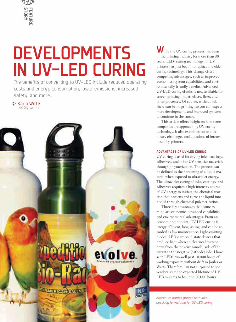
Aluminum bottles printed with inks specially formulated for UV-LED curing

march/april 2012 | 23
The advanced capabilities available in the market today represent the newest de-velopments allowing for heat-sensitive sub-strates, deep-through cure, small, compact machines with controlled curing intensity. Similar advancements have impacted the environment factor. The current emphasis is better than ever on workplace safety. Devices are now both mercury and ozone free, and there is greater interest in UV-A wavelength range.
Looking at ink technology today, you can start by examining the challenges of current UV-LED light sources. From a sim-ple point of view, power is a direct function of wavelength, so the lower the wavelength, the more difficult it is to achieve power output. It is also generally accepted that the power of the UV LED rapidly dissipates as the distance from the source increases. There is no established standard measure-ment of power output from UV LED; therefore, the output is often measured at the light source.
For printing applications such as web and inkjet, it’s possible to get the source very close to the print surface, minimizing the loss of output power. For applications such as screen and sheetfed printing, the distance of the print surface from the light source is greatly increased, so understand-ing the energy output at the print surface becomes critical.
To help overcome this, UV-LED light suppliers are studying the effect of peak in-tensity versus total UV exposure, and they are looking at ways of distributing the en-ergy output over distances using proprietary and patent or patent pending techniques, much like during the initial development of mercury arc UV for printing.
Current UV-LED light also produces a distinct, single-peak-intensity profile centered on a single wavelength. The major wavelength ranges emerging are at 385-395 nm (with some centering at 390 nm), and 365 nm. For printing ink, this presents obstacles that include the need to use photoinitiators that absorb into the visible light spectrum, affecting on-press stability as the visible light in a print operation can polymerize the ink on press.
march/april 2012 | 23
VACUUM TABLES
We Ship Worldwide
Manufacturer of theLargest Tables in the World
ACCU-PRINT HIGH-TECH™ SERIESFlatbed Screen PrinterS For every budget and Job
Accu-PrintHigh-Tech Micro™
773.777 3.777.0909@ i . i.com
Accu-PrintHigh-Tech HL™

24 | IndustrIal + specIalty prIntIng www.industrial-printing.net
The lack of energy in the UVB and UVC wavelength affects the ability to cure ink at the print surface, often due to oxygen inhibi-tion. For coatings, additional challenges of yellowing from photo initiator can occur without using photo initiators that absorb in the UVB and UVC ranges.
new developments aId screen prIntIngThese challenges have not stopped the use of LEDs with today’s printing technology. The advances in UV-LED power output were first used in commercial inkjet printing, with companies displaying the ability to produce narrow-web inkjet labels at speeds up to 80 ft/min.
The advantages of UV-LED for inkjet include: a smaller foot-print for the unit, the instant on/off or adjustable capability, no generation of IR for the light source, and no generation of ozone. The intensity of UV LED can be altered, just like a dimmer switch at home. This capability allows print shops to add specialty details such as matte or gloss or special effects. And the visible-light-sta-bility challenges are minimized as the ink is not readily exposed to light prior to curing.
As for screen printing, the advances in LED lamp technology and UV screen-printing ink formulations have proven LED curing as a viable alternative to medium-pressure mercury lamps. Chad Taggard, the VP of marketing for industry supplier Phoseon Tech-nology, said recently that “printers using UV-curable inks should have units to measure the energy of any type of curing device.” This equipment will advise you to the amount of Watts and Joules that your ink/substrate achieves during exposure. A chemist then can create a formula that will cure based on this information. The print operator should then test the unit frequently to maintain the proper curing energy. It’s also important to use a testing device that works with UV LED, not just a UV device, because it would provide the wrong information.
Not long ago, UV screen inks could not be used with LED cur-ing because they did not have the processing latitude to overcome the restrictions of using LED lamps. Restrictions included lower wattage and single-nanometer output.
The newest screen-ink technologies now formulate viable specialty inks that cure exceptionally well with 4- and 8-w LED
395-nm lamps at belt speeds of 30-120 ft/min. This curing-speed range relates to the ink’s color, the thickness of ink deposited, and the substrate color.
As for applications that best fit this type of curing, films truly suit LED because the LED projects very little heat towards the substrate. LEDs are lightweight when mounted to the carriage, which is why smaller digital printers use LED. UV-LED lamps work well with any applications where the curing system can be within 25 mm of the curing substrate.
Initial research has already shown that 365-nm UV provides better surface curing in a dark colored flexo ink, while having inferior cure at the print surface. Adding the higher energy output 385-nm UV-LED light source inline with the 365-nm light source had positive effects on the ink surface and substrate interface for curing (Figure 1). The belief is that as higher output UV-LED light sources are developed, the cure deficiencies may be overcome in the single-peak-irradiance-wavelength systems.
Other ink developments include research into studying the impact of lack of IR heat on the curing process with UV LED and looking at how single-wavelength UV light may impact the overall adhesion of ink to a variety of substrates. Studies also are underway on the potential of photoinitiators specifically formulated to optimize curing with the UV-LED wavelengths, noting that getting regulatory approval on novel chemistries requires long-term development.
lookIng at the bottom lIneOverall, the market is starting to see the addition of practical lamps and inks. The benefits of converting to LED curing are nu-merous, including the reduction of operating costs, reduced emis-sions, and the use of mercury bulbs, as well as increased safety and a huge reduction in energy usage. It’s important to note that LED costs more than mercury-lamp systems. The up-side here is the consumable costs are eliminated, and so is the expense for blowers, ballasts, and other peripherals.
If considering an investment in UV-LED curing, first prepare an ROI assessment to justify the cost of making a switch to LED from other curing types. Operating costs are significantly lower with UV LED. UV LED can be turned on or off instantly with no warm up time required. Printers who take advantage of this can significantly reduce their operating costs.
Printers also need to keep in mind that thinner and/or heat-sensitive substrates can be used with UV LED. Not only does this open the doors to potential new revenue streams, but it also reduces shipping and storage costs. It is possible that a print shop might save 30 % on shipping costs alone.
Karla Witte is the VP of product development for INX Digital Int’l Co. She has been involved in digital printing of fine and graphic art for 19 years and has also worked for Harvest Productions/BullDog Products. She can be contacted at [email protected].
karla wItteINX Digital Int’l
Figure 1 Overlay of AMS 390 nm and 365nm UV-LED lamp intensity compared to standard, medium-pressure mercury-vapor arc UV. Photo courtesy of Air Motion Systems U.S.A.
radI
ant
Inte
nsIt
y (a
u)
wavelength In nanometers (approxImate)led uv 365 led uv 390 mercury lamp
MARCH/APRIL 2012 | 25
FEATURE STORY
As printed-electronics applications continue to expand and merge technologies between traditional, polymer thick- lm, rigid/ ex-circuit and electronic-assembly applications, the require-ments for functional, printed inks are being pushed to new limits. Electrically conductive and resistive inks, UV-curable dielectric insulators, conductive adhesives, UV-curable encapsulants, and others that have been used in more traditional PTF-device manufacturing, such as membrane switches and EL panels, must be able to be adapted to the emerging, and often more stringent, requirements of the latest printed-electronics applications.
New substrates and methods of application require changes to polymers and solvents traditionally used in PTF applications. To do this, it is essential to have an understanding of some of the practical limits these materials have when exposed to harsh environments and how to design devices around the limitations of the functional ink materials.
OBJECTIVEUsing a specially designed circuit con guration (Figure 1) that incorporates serpentine patterns, surface-mount pads, and crossover multilayer printed traces that are typically found in PTF printed devices, circuits were printed at three different printing facilities using different combinations of silver inks, UV dielec-trics, low-temperature curable-surface-mount epoxies and encap-sulants, and carbon inks. The three printing facilities were ECI Screenprint in Thompson, CT; GM Nameplate, Inc. in Seattle, WA; and Dawar Technologies in Pittsburgh, PA.
After printing, surface-mount resistors were placed by Nico-matic LP in Warminster, PA. Final assembly was performed at ECI Screenprint and then product testing was performed at Conductive Compounds, Inc. in Hudson, NH. PET lms used as substrates were standardized for all printers, and printers were in-structed to use their best manufacturing practices that they would typically use for membrane-switch printing. All inks and materials were supplied by Conductive Compounds, Inc.
Don Banfi eld, Ryan Banfi eld, and Miranda LawrenceConductive Compounds
e tests performed here were intended to show how some commonly used functional inks fail when pushed to extremes in heat, humidity, and water in printed-electronic applications.
PROCEDUREDifferent copolymer combinations used in the silver inks included polyester, vinyl, and urethane. UV-curable dielectric insulating inks were urethane acrylate copolomers with matte and glossy nishes, and materials were evaluated as undercured and overcured with a Medium Pressure Mercury Vapor (MPMV) UV lamp. Surface-mount epoxies were two-part, low-temperature polymer systems typically used in PTF manufacturing, and epoxy evaluation was done with various ratios of part A to part B to investigate effects of incorrect mixing on polymeric properties.
Because the materials selected are widely used in all areas of PTF-device manufacturing and have passed the rigors of appli-ance, medical, and automotive testing, it was necessary to push the conditioning and testing to further limits to force failures within the functional inks to try to see which component(s) of the inks would fall out rst under adverse conditions. Typical conditioning of test samples were:
85°C, 100% Rh, 1000 hoursImmersion in water at 40°C for seven days150°C bake at ambient Rh until failure
Mechanical and electrical properties of test circuits were mea-sured both before and after exposure. Two levels of testing were em-ployed on the circuits and functional ink materials. First, testing and inspection of the circuits was performed using the following criteria:
Point-to-point electrical resistance on silver and carbon ink tracesLow-voltage resistance across 500 ohm surface-mount resistors Destructive AC high-voltage-breakdown test through crossover multilayer patterns Visual inspection of circuit materials and surface-mount joints
Second, the functional ink materials were analyzed using sophis-ticated laboratory equipment to try to determine how the materials
•••
•
••
•

26 | IndustrIal + specIalty prIntIng www.industrial-printing.net
changed physically during testing and how these changes might lend themselves to potential failures in a printed electronics application. Below is a list and description of the test devices used as applicable:
thermogravImetrIc analysIs, TGA, measures weight loss very accurately at specified temperature ranges. This can be used to evaluate solvent and volatiles coming off of a material or at elevated temperatures up to 1000°C it is possible to burn off all polymeric material, leaving behind metal and inorganic fillers.
FourIer transForm InFrared spectroscopy, FTIR, gives a unique fingerprint of a polymer material by exposing it to a scan of the full wavelength infrared spectra. At different frequencies of IR, different combinations of atoms on a molecule will absorb the IR energy, so the fingerprint scan shows IR absorption by a polymer at different frequencies of energy. If a polymer undergoes any chemical changes at all, the FTIR scan will be different.
dIFFerentIal scannIng calorImetry, DSC, measures the heat flowing into or out of a very small sample as it is heated by the instrument. This allows accurate measurement of properties such as melting points, activation time for epoxy curing, and crystallization points. The DSC can measure this by adding heat to a polymer or by exposing the polymer to specific bands of UV energy for UV-cured polymers.
thermomechanIcal analysIs, TMA, measures the expansion of a material accurately as it is exposed to heat. It can also measure the deflection of a fixed, constant weight into a polymer material as it is heated. This allows properties such as coefficient of thermal expan-sion (Cte) and glass-transition temperature (Tg) to be evaluated. This allows us to understand how functional inks and materials will work in an assembly as the device is heated and cooled and the various materials it contains expand and contract at different rates.
tensIle/elongatIon testing allows studying of the mechanical strength and elongation of materials. This testing is valuable not only as a benchmark to compare different materials, but also to look at the effects of undercuring materials and exposing them to heat and/or moisture.
scannIng electron mIcroscope, SEM, allows us to look at functional ink materials at exceptionally high magnifications—as high as 100,000x. This lets us see effects such as packing efficiency of filler materials and whether there is any evidence of fusing of the filler materials.
resultsThe test results showed some expected and surprising results. Starting with an analysis of the performance of the UV curable, screen-printable dielectric/insulator inks, results indicated the need for two-pass applications of these materials to achieve reliable electrical insulation between two layers of conductors. Two different industry-standard acrylate function dielectric formulations (matte and glossy) were paired with silver inks made using more common polyester and vinyl copolymers to see if any interactions would show up during testing.
Because the crossover-voltage test was destructive and failure ranges varied significantly, the results were tallied by percentage of failure of test samples at high voltage. Notice that the figure has two legends—one print pass and two print passes, yet there is only one set of bars on the chart for the two print passes. This is because ev-ery single sample of the one print pass dielectric failed at significant-
Pre Post
50
45
40
35
30
25
20
15
10
5
0 Vinyl, Matte
Vinyl, Glossy
Polyester, Matte
Polyester, Glossy
Resi
stan
ce Ω
overcure undercure
10%
9%
8%
7%
6%
5%
4%
3%
2%
1%
0%UV 2530 UV 2531 UV 2534 UV 3010
Figure 1 This specially designed circuit configuration incorporates patterns, pads, crossovers and traces typically found in PTH printed circuits.
Figure 2 The effect of heat and moisture on conductive inks and UV dielectrics when exposed with and without graphic overlay materials lami-nated onto them.
Figure 3 The weight loss percent by TGA of several different industry-standard UV materials.
Figure 4 A typical vinyl copolymer silver ink pattern before and after heat and humidity exposure
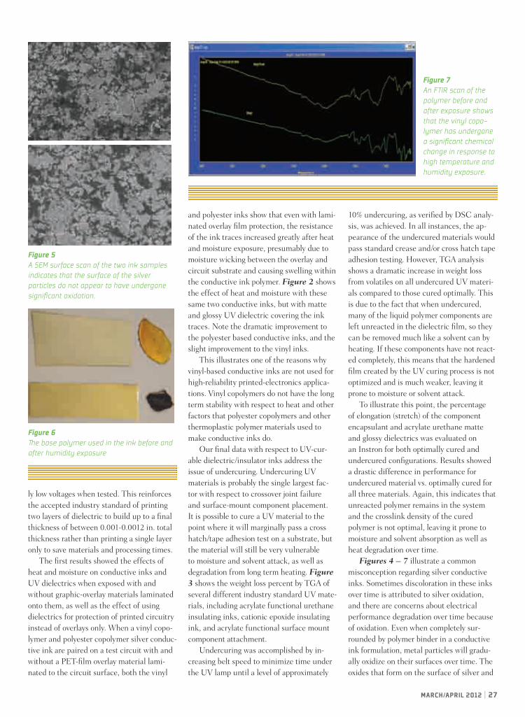
march/april 2012 | 27
ly low voltages when tested. This reinforces the accepted industry standard of printing two layers of dielectric to build up to a final thickness of between 0.001-0.0012 in. total thickness rather than printing a single layer only to save materials and processing times.
The first results showed the effects of heat and moisture on conductive inks and UV dielectrics when exposed with and without graphic-overlay materials laminated onto them, as well as the effect of using dielectrics for protection of printed circuitry instead of overlays only. When a vinyl copo-lymer and polyester copolymer silver conduc-tive ink are paired on a test circuit with and without a PET-film overlay material lami-nated to the circuit surface, both the vinyl
and polyester inks show that even with lami-nated overlay film protection, the resistance of the ink traces increased greatly after heat and moisture exposure, presumably due to moisture wicking between the overlay and circuit substrate and causing swelling within the conductive ink polymer. Figure 2 shows the effect of heat and moisture with these same two conductive inks, but with matte and glossy UV dielectric covering the ink traces. Note the dramatic improvement to the polyester based conductive inks, and the slight improvement to the vinyl inks.
This illustrates one of the reasons why vinyl-based conductive inks are not used for high-reliability printed-electronics applica-tions. Vinyl copolymers do not have the long term stability with respect to heat and other factors that polyester copolymers and other thermoplastic polymer materials used to make conductive inks do.
Our final data with respect to UV-cur-able dielectric/insulator inks address the issue of undercuring. Undercuring UV materials is probably the single largest fac-tor with respect to crossover joint failure and surface-mount component placement. It is possible to cure a UV material to the point where it will marginally pass a cross hatch/tape adhesion test on a substrate, but the material will still be very vulnerable to moisture and solvent attack, as well as degradation from long term heating. Figure 3 shows the weight loss percent by TGA of several different industry standard UV mate-rials, including acrylate functional urethane insulating inks, cationic epoxide insulating ink, and acrylate functional surface mount component attachment.
Undercuring was accomplished by in-creasing belt speed to minimize time under the UV lamp until a level of approximately
10% undercuring, as verified by DSC analy-sis, was achieved. In all instances, the ap-pearance of the undercured materials would pass standard crease and/or cross hatch tape adhesion testing. However, TGA analysis shows a dramatic increase in weight loss from volatiles on all undercured UV materi-als compared to those cured optimally. This is due to the fact that when undercured, many of the liquid polymer components are left unreacted in the dielectric film, so they can be removed much like a solvent can by heating. If these components have not react-ed completely, this means that the hardened film created by the UV curing process is not optimized and is much weaker, leaving it prone to moisture or solvent attack.
To illustrate this point, the percentage of elongation (stretch) of the component encapsulant and acrylate urethane matte and glossy dielectrics was evaluated on an Instron for both optimally cured and undercured configurations. Results showed a drastic difference in performance for undercured material vs. optimally cured for all three materials. Again, this indicates that unreacted polymer remains in the system and the crosslink density of the cured polymer is not optimal, leaving it prone to moisture and solvent absorption as well as heat degradation over time.
Figures 4 – 7 illustrate a common misconception regarding silver conductive inks. Sometimes discoloration in these inks over time is attributed to silver oxidation, and there are concerns about electrical performance degradation over time because of oxidation. Even when completely sur-rounded by polymer binder in a conductive ink formulation, metal particles will gradu-ally oxidize on their surfaces over time. The oxides that form on the surface of silver and
Figure 5 A SEM surface scan of the two ink samples indicates that the surface of the silver particles do not appear to have undergone significant oxidation.
Figure 7 An FTIR scan of the polymer before and after exposure shows that the vinyl copo-lymer has undergone a significant chemical change in response to high temperature and humidity exposure.
Figure 6 The base polymer used in the ink before and after humidity exposure

28 | IndustrIal + specIalty prIntIng www.industrial-printing.net
gold particles remain highly conductive compared to the oxides that form on other metals such as copper or aluminum. For this reason it is necessary to use the more expensive metals when formulating conductive inks.
Even when exposed to ambient temperatures over time, many conductive inks will undergo a slight discoloration. This is more pronounced with vinyl and some urethane copolymer inks than with polyester or some other types of thermoplastics. A common perception is that this discoloration (usually a brownish or yellowish light coloration) is due to metal oxidation. Figure 4 shows a typical vinyl copolymer silver ink pattern before and after heat and humidity exposure. Note the light brown coloration after exposure. Figure 5 shows a SEM surface scan of the two ink samples, indicating that the surface of the silver particles do not appear to have undergone significant oxidation. Figure 6 shows the base polymer used in this ink both before and after heat and humidity exposure. There is a dark discoloration of the polymer after exposure. An FTIR scan of the polymer both before and after exposure (Figure 7) shows clearly that the vinyl copolymer has undergone a significant chemical change in response to the high temperature and humidity exposure.
The final data sets presented focus on the surface-mount aspects of printed electronics. Because of the unique requirements of PE ap-plications, often the substrates used are extremely thin and flexible, and cannot be exposed to high temperatures. Because most of these substrates are polymeric, adhesion of the surface-mount epoxy can be difficult. Temperature limitations of these polymeric substrates require that the vast majority of surface-mount applications in PE use two-part epoxy adhesives, which are able to cure at very low temperatures but have the disadvantage of short pot life (working time) after mixing.
One of the frustrating aspects of trying to analyze surface-mount failures in printed electronic applications is that often the failure shows up as a latent defect, meaning that it passes testing after manufacturing but then shows up as a failure sometime after the customer receives it. Often the factors that contribute to this (incor-rect curing of conductive epoxy, improper component placement, incorrect mixing of epoxy, and improper ink trace design) cannot be isolated and identified after manufacturing.
It is nearly impossible to properly analyze a PE surface-mount joint to investigate means of failure. Often you will find a failed surface-mount joint, but the surface mount component sitting close to the failed joint does not fail, and often will even withstand an ag-gressive flex/crease test without failing. For this reason, it is essential to follow good manufacturing practices as recommended by suppliers in order to minimize the impact of these factors on potential surface-mount failure.
Because of the potential for joint failure when attaching LEDs, resistors, or other components onto flexible thin films, it is advised to use center-stake adhesives such as one-part cyanoacrylates and clear, UV-curable encapsulants to cover the component completely after it has been surface mounted to the substrate. Figure 8 shows the results of four different construction methods after long-term immersion in hot water with respect to the number of extreme (out of spec) readings obtained when measuring resistance through a sur-face-mount joint and across a discrete resistor. The four construction methods used were conductive epoxy only, conductive epoxy with center stake adhesive, conductive epoxy with clear UV encapsulant
only, and conductive epoxy with center-stake adhesive and clear UV encapsulant. Note the dramatic improvement in surface-mount joint reliability on the two construction methods that use the clear UV encapsulant to seal and protect the component and surface-mount joint from moisture.
Figure 9 further illustrates the effect of providing some protec-tion to the surface- mounted component and joints by comparing the number of failures on surface-mounted components both with and without a laminated polymer film overlay to protect them during long term water immersion.
A common cause of surface-mount joint failure in printed elec-tronics is incorrect mixing of resin to hardener. Most epoxy formula-tions require precise mix ratios with a tolerance of ±1% by weight to optimize the mechanical properties of the conductive epoxy. Care-less or incorrect weighing errors can easily push this tolerance out to ±5% or more. Figure 10 shows the effect of a common two-part conductive epoxy adhesive that has both an abundance of curing agent added to it, and a shortage of curing agent. For this test, an optimal mix was prepared, as well as a mix with 5% less curing agent
Figure 8 The results of four different construction methods after long term hot water immersion
50%
60%
40%
30%
20%
10 %
0%
% Extreme Surface Mount Resistance readings (Post Immersion Test) Sorted By Surface Mount Material Combinations
60%
80%
40%
20%
0%
Extreme Surface Mount Resistance Readings Coverlay Vs. No Coverlay
With Coverlay
Without Coverlay
Figure 9 The effect of providing some protection to the surface-mount component and joints
36%
38%
34%
32%
30%Optimal -5% CA +5% CA
14.2% Difference
Epoxy with Optimal, 5% Less And 5% More Cuting AgentFigure 10 The effect of a common two-part conductive epoxy adhesive that has an abundance of curing agent added and a shortage of curing agent
march/april 2012 | 29
and 5% more curing agent. The samples were cured to completeness, and the TGA was used to evaluate weight loss at very high temperature.
Figure 10 shows the actual TGA scan to the left, and then a table of weight loss of the three different epoxies to the right. Note that the two configurations with less and more curing agent showed a significantly higher amount of weight loss during burn off in the TGA than the sample that was weighed and mixed correctly. This shows that if these two part epoxy materials are not weighed and mixed correctly, surface-mount joint integrity will be compromised because there is a lot of volatile, unreacted polymer in the materials that over time will act as solvents and begin to leach out of the material.
To capitalize on the rapidly emerging opportunities within printed electronics, it is essential that manufacturers learn some of the material science behind these inks and have access to analytical equipment that can help them explore and understand the limits of the materials. Printed electronics continues to have a stigma of the Wild West attached to it, but collaborations between suppliers, printers, and OEM manufactur-ers can help push the boundaries of what functional ink materials and substrates are capable of accomplishing.
Don Banfield is product manager and co-founder at Conductive Compounds, Inc., Hudson, NH. Conductive Compounds Inc. develops and manu-factures materials for the global electronics as-sembly market. In addition to standard products, the company specializes in custom formulations for new high-tech applications in the printed electronics industry.
Don BanfielDConductive Compounds
Ryan Banfield is a materials science engineer and sales engineer for Conductive Compounds, Inc.
ryan BanfielDConductive Compounds
Miranda Lawrence is a student intern at Conduc-tive Compounds, Inc. from Northeastern Univer-sity, Boston, MA.
miranDa lawrenceConductive Compounds

30 | IndustrIal + specIalty prIntIng www.industrial-printing.net
feature story
opportunities for silver Inks and pastes in a declining Market
Jill Simpson, Ph.D.NanoMarkets
ket emerged. The question now is: What’s next thing that will increase the size of your addressable market for silver?
changIng Markets for sIlverWe believe that, eventually, the next big thing for printed silver will be printed, flexible, and perhaps transparent electronics applications, especially for applications that enable ubiquitous and/or wireless sensing and computing for the internet of things in both the medical and everyday consumer information spheres. The potential for these kinds of applications deserves some skep-ticism, but we think that the tide may be turning in their favor in the mid-term. We also think that these new applications are not going to develop quickly enough to offset declines.
A breakdown of the market reveals that two applications dominate consumption: the traditional thick-film, printed-cir-cuitry applications, and the photovoltaics market (Figure 2). In recent years, the photovoltaics market has overtaken traditional thick-film applications as the single biggest user of silver inks and pastes. But both of these applications are very cost sensitive, and both, in different ways, are facing difficult times ahead.
The PV market had a very good year in 2010, with nearly 150% growth over 2009. For 2012 and forward, we anticipate, obviously, much lower growth rates, around 15% per year. Meanwhile, for a couple of reasons, we are also predicting a decline in consumption of silver in the PV market. First, there is an ongoing, gradual shift in relative importance of thin-film PV, which uses very little silver, compared to crystalline silicon PV, which uses a lot of printed silver. At the same time, the way that silver is consumed in crys-talline-silicon PV is changing. While front-side printed silver grids appear safe, and even growing, backside electrodes are facing seri-ous competition from aluminum, and printed silver tabbing strips are being increasingly replaced with solders.
In addition, government support for PV is waning. Govern-ments around the world are looking for ways to cut their budgets, and of course things like tax incentives, feed-in tariffs, and subsi-dies for PV are a natural target for the axe. Panel makers cannot be so certain anymore that governments around the world will continue to provide financing for PV.
The other big consumer of printed silver is the thick-film ink and paste market. The thick-film printed-silver market is not in decline, but we are expecting relatively slow growth over the next decade. A contributing factor to the slow overall growth is that plasma display panels are in decline. They are being gradually displaced by LCDs, which will account for almost $300 million in lost revenue between now and 2019. Meanwhile, high silver prices do encourage substitution away from silver. In the past, when silver prices spiked, cheaper conductive alternatives have always increased in popularity, but they usually faded into the back-ground when silver prices fell again. Today, however, persistently high silver prices may present a sustained opportunity for some of the cheaper alternatives to actually make a dent in silver inks.
opportunItIes aMIdst the troubleOf course, the news is all bad. First of all, there is no reason-able substitute for silver in most applications. Other metals with reasonable conductivity are available, but they are, for the most part, insufficiently conductive or too oxidation-prone for the most demanding printed silver applications. Nonmetallic conductors—
Find out why silver is sliding and discover where profits may be found when working with inks based on this precious metal.
Suppliers of silver printing materials are facing a big problem today related to the high price of silver. Suppliers of silver inks and pastes to the electronics industry face the challenge of how to maintain profitability and market share in a world with persistently high silver prices with no clear end in sight.
Average silver prices were higher than ever in 2011, at just more than $35 per ounce. A high level of investment offtake of silver for monetary hedging is keeping silver prices high. Silver prices rose more than 140% over the 2009-2011 timeframe, and some industry experts are predicting that the metal will go even higher in the next few years. It seems almost certain that low silver prices will not reappear any time soon. Fiscal uncertainty and high debt in important markets in the U.S. and Europe, along with lackluster economic growth, is keeping investment in silver metal high.
In this new environment, NanoMarkets is in the unusual position of predicting a decline in global silver inks and paste consumption, in both value and volume terms. Specifically, our forecast for silver inks and pastes consumption for 2012 is about $7.5 billion, and we see the value of the market softening to about $7 billion by 2019.
Suppliers of silver printing materials are facing a new world, one that is much different from the one they have been in for the last 50 years or so. Overall, this industry has had a very good run over the last several decades, in which the post World War II boom in consumer electronics, appliances, microwaves, refrigerators, etc. were the first big users of printed silver. When that market started to stabilize, the computing revolution arrived, and with it came a whole new addressable market for printed silver for microcircuitry in cell phones, computers, and the like (Figure 1). Then, in recent years, the crystalline-silicon PV mar-

march/april 2012 | 31
conductive polymers, carbon nanotubes, graphene, etc.—are also often cited for their potential in printed-circuitry applications. But all of these also are very small players, at least for now, and prob-ably can only threaten printed silver on the fringes of the market.
Second, the thick-film legacy applications will benefit from global industrialization that will drive growth in consumer electronics. And the general trend toward miniaturization in electronics provides new opportunities for suppliers to provide value-added materials that enable higher resolution.
So, how does a supplier get into this market? Suppliers may also seek to offer drop-in replacements for the existing competi-tion, but finding customers with sufficient incentive to switch to a me too product is difficult. Alternatively, they may offer products that require a change in process, but the costs and risks associ-ated with switching existing production lines over to a new kind of process are often understated.
Instead, NanoMarkets thinks that a better approach is to prod-ucts that enable new applications, in markets that are not yet fully formed. Examples are: nanosilver inkjet inks that enable minia-turization for new kinds of sensors for pervasive electronics, inks that will enable flexible interconnection in flexible displays, or inks that enable larger panel sizes in the nascent OLED lighting market. There are also opportunities in new ink and paste markets that aren’t really fully formed yet. Supplying emerging markets is risky, but the rewards can be great, and the emerging nature of these markets also means that suppliers have time to work closely with customers to get into the development cycle.
The case for nanosilverNanosilver has been on the scene for a while now. When it first emerged, there was a lot of hype surrounding it, and the expecta-tions were that it would revolutionize the electronics industry. The nanosilver revolution did not happen, and it became reason-able to ask whether it ever would.
Thus far, economies of scale for nanosilver have not been achieved. Nanosilver also faces an uncertain and potentially complicated regulatory environment, especially in the EU, and, to a lesser extent, in the U.S. Market pull for printed-electronics applications for nanosilver has not materialized.
There is good news for nanosilver, though (Figure 3). The aforementioned miniaturization trend and need for high resolution in electronics is tailor-made for nanosilver. In addition, the sus-tained high silver prices have a less negative effect on nanosilver than on conventional silver printing materials. These factors mean that there is an opportunity opening up for nanosilver to be more seriously evaluated in different kinds of applications.
how To sTay afloaTIn summary, the market for silver inks and pastes will decline over the next couple of years, but that doesn’t mean there aren’t places to make money. First, products that reduce costs through reductions in precious-metal usage are in demand, especially in the conventional thick-film and PV applications. Next, materials that enable miniaturization through high-resolution, fine-line printing will see increased demand, as will materials than that enable ubiquitous electronics, sensing, and computing. Finally, for suppliers that depend on the PV market, diversification into other markets may be necessary to maintain revenue levels.
Overall, the market for printed silver is entering a period of reduced volume. Suppliers will need to reorganize around newer businesses and newer applications, and marketing and business development strategies will require rethinking. Increased partner-ing and collaboration will be necessary to identify new applica-tions, which may be increasingly found in riskier, yet higher value, products.
Jill Simpson, Ph.D., is senior analyst of NanoMarkets based in Glen Allen, VA. NanoMarkets is a market research and industry analysis firm that looks at opportunities within the advanced materials, energy, and electronics areas.
Jill simpson, ph.D.NanoMarkets
8000
7000
6000
5000
4000
3000
2000
1000
02012 2013 2014 2015 2016 2017 2018 2019
Traditional Thick Film
Sensors
RFIDs
OLED Lighting
PDPs
Photovol-taics
$7.6 B
$6.8 B
Figure 1 Silver Inks and Pastes 2012-2019 by Application ($ Millions)
45004000350030002500
200015001000500
02012 2013 2014 2015 2016 2017 2018 2019
- 200- 180- 160- 140- 120- 100- 80- 60- 40- 20- 0
Valu
e ($
Mill
ions
)
Addressable Market ($M
illions M2)
Value of Printed Silver in TFPV
Value of Printed Silver in c-Si PV
c-Si Addressable
Market
TFPV Addressable
Market
Figure 2 Silver Inks and Paste in PV by Application 2012-2019
2012 2013 2014 2015 2016 2017 2018 2019
50045040035030025020015010050
0
~12x
~2.4x
~3x~1.7x
Average Nanosilver
ink/Paste Price
Average Conventional
Silver ink/Paste Price
Average Nanosilver
ink/Paste Price
Figure 3 Average Ink and Paste Prices ($ / Troy Oz. Silver)

32 | IndustrIal + specIalty prIntIng www.industrial-printing.net
aIXtrOn tools Installed at graphene research lab AIXTRON SE installed two BM Pro, formerly known as Black Magic, 4-in.-wafer-deposition tolls to the Italian Institute of Technology (IIT) in Pisa, Italy, for the development and production of graphene in hydrogen storage systems. IIT Pisa will use one system to deposit graphene using chemical vapor deposition and plasma-enhanced chemical vapor deposition. The BM Pro system is for use in high-temperature (1800˚ C) processing, which forms graphene using sublimation. These two tools will assist the Institute’s research on graphene film for nanoelectronics and energy storage devices.
Industry neWs
Market m
ovements and association updates
BMG Forges Licensing Agreement with KodakSarasota, FL-based Brand Management Group (BMG) will sell Kodak wide-format inkjet media products to imaging professionals in the wide-format print-for-pay, professional photography, fine-art reproduction, sign, in-house corporate graphics, point-of-purchase graphics, advertising, exhibit, and reprographics markets through a worldwide network of distributors and re-sellers. The trademark licensing agreement was signed in fourth quarter of 2011 and commenced effective January 2, 2012.
Soitec Secures Financing for Solar Plant in South AfricaBernin, France-based Soitec, manufacturer of semiconductor materials for the electronics and energy industries, has secured financing from Investec Bank Ltd. to build the company’s 50-megawatt-peak solar-power plant in South Africa. Investec has committed to finance the project and raise the equity to construct the plant. All financial arrange are expected to be finalized by Q2 of 2012, the company says.
Roland DGA Announces Creative Awards Contest ResultsRoland DGA announced its top regional award winners of the Roland Creative Awards international design contest as well as Honorable Mention and January People’s Choice Award recipients for the North American region. All winning entries receive prizes and recognition, with the overall winners in each region going to Japan to compete for the worldwide grand prize, the Roland machine of their choice. A gallery of all winning en-tries worldwide can be viewed online at www.rolandcreativeawards.com/winners.
regional award Winner: Gamut Media, Brea, CA—Saladish Honorable Mention award Winners: AC Golden Design, Los Angeles, CA—Bonsey Pendant; Bennett Bean Studio, Blairstown, NJ—Ceramic SculptureMonthly people’s choice award Winner: Loudmouth Printhouse, ONT—Devil Inside
Auto Infotainment to Grow in 2012Automotive infotainment revenue in 2011 amounted to $32.5 billion, up 3.4% from 2010, according to an IHS iSuppli Automotive Infotainment Semiconductor Market Tracker report. Revenue in 2012 is projected to surge to $33.5 billion, and growth will be even stronger in the next four years, ranging from 4.7-6.4 %. By 2016, the market will reach $41.2 billion, according to IHS.
Automotive infotainment equipment represents a range of electronic devices con-cerned with a vehicle’s delivery of information and entertainment content to its occu-pants. The field includes areas like navigation systems, premium audio, telemetric, fuel efficiency, safety and connectivity solutions.

march/april 2012 | 33
On the moveQuadrant Engineered Plastic Products of Read-ing, PA, appointed Charlie Costello to regional sales manager in the Midwest region. Cincinnati, OH-based TAPPI has elected Steven J. Shiftman, president and CEO of Michelman, Inc., to serve on the 2012-2014 TAPPI board of directors.
Shiftman
Transparent Conductors for PV to Grow in 2012The total market for transparent conductors (TC) in the photovol-taics (PV) industry is predicted to grow at a CAGR of more than 30% from a value of $90 million in 2012 to $300 million in 2016, according to a report from Nanomarkets, an industry forecast and analysis firm. PV markets are shifting, says the report. Major PV application markets covered include thin-film Si PV, CDTe PV, CIGS PV, OPV, and DSC. The report talks about decreased government support for the TFPV market. The largest prospect for TCs lie with solution-processable nanomaterials.
LG Chem Starts Mass Production of OLED PanelsLG Chem finished the development phase of its OLED lighting panel and will begin mass production. The type 1 panel, the LG OLED-041 is a 100 x 100-mm panel that features 4,000K, CRI >80, 45 Im/W and 10,000-hr lifetime (LT70) at 3000 nits. The active emitting panel is 90 x 90 mm, and the whole panel is 2.44 mm thick.
LG Chem is developing the second-generation panel, which will up the efficiency to 60 Im/W and the lifetime to 15,000 hr. The size will be the same, but the color will be 3,500K. LG is said to start mass production of type 2 panels in Q2 of 2012.
SEND US YOUR NEWSEmail [email protected]
DuPont and Suntech Sign Strategic AgreementDuPont and Suntech Power Holdings Co, Ltd., one of the world’s largest producers of solar panels, have signed a strategic agree-ment to help increase the supply of photovoltaic materials and technologies for the growing global market for solar energy. The agreement focuses on technology advancements, supply-chain optimization, cost-reduction initiatives, and DuPont’s Tedlar polyvinyl fluoride film supply. The companies also are pursuing co-marketing opportunities. The goal is to achieve faster and broader adoption of solar energy to reduce the world’s dependence on fossil fuels. They intend to achieve the goal by further improv-ing the technology for solar energy and helping reduce its costs and building greater awareness of its benefits to consumers.
“We’re partnering with leading PV-component suppli-ers around the world as we continue to make solar affordable for everyone, everywhere,” says Eric Luo, senior VP of global supply chain, Suntech. “Creating higher efficiency solar cells and further extending the long life of solar modules is critical to achieving affordable solar power, and we’ve worked closely and very success-fully with DuPont in this regard. We’re taking our collaboration to the next level with this agreement.”
Ellsworth Continues Mexico ExpansionGermantown, WI-based Ellsworth Adhesives has expanded to larger facilities in Tijuana and Guadalajara, Mexico. The company is a global distributor and provider specializing in adhesives, seal-ants, lubricants, coatings, encapsulants, tapes, soldering products, surface preparations, specialty chemicals, maintenance and repair products, and dispensing equipment.
“Ellsworth has achieved explosive growth in Mexico in the past few years, and we are excited about the expansion in Tijuana and Guadalajara,” says Roger Lee, VP and general manager.
INX Partners with Giant MediaINX Digital Int’l agreed to partner with Giant Media, LLC. In the wide-format industry Giant Media will sell INX Digital’s alterna-tive line of products, including eco TRIANGLE EDX inks.
Phoenix, AZ-based Giant Media provides equipment supplies, software, and consumables to the signage and graphics industry. Giant Media is in the process of securing an additional distribu-tion facility in the Midwest to offer faster service to customers in that area. INX Digital introduced EDX inks in 2010. Since then, it has been used in the wide-format market.
Blue Spark Opens Battery-Printing Facility Cleveland, OH-based Blue Spark Technologies, supplier of thin, flexible, eco-friendly printed batteries has opened a high-volume printing and production facility in West Bend, WI. The new facil-ity extends Blue Spark’s capability to produce large volumes of its line of disposable, flexible, carbon-zinc batteries to meet growing demand for printed electronics that power innovations in commer-cial and industrial packaging.
“Our investment in the new Wisconsin facility demonstrates our operational readiness to support wide range market adop-tion of thin printed batteries that bring power to packaging,” says company president and CEO John Gannon.
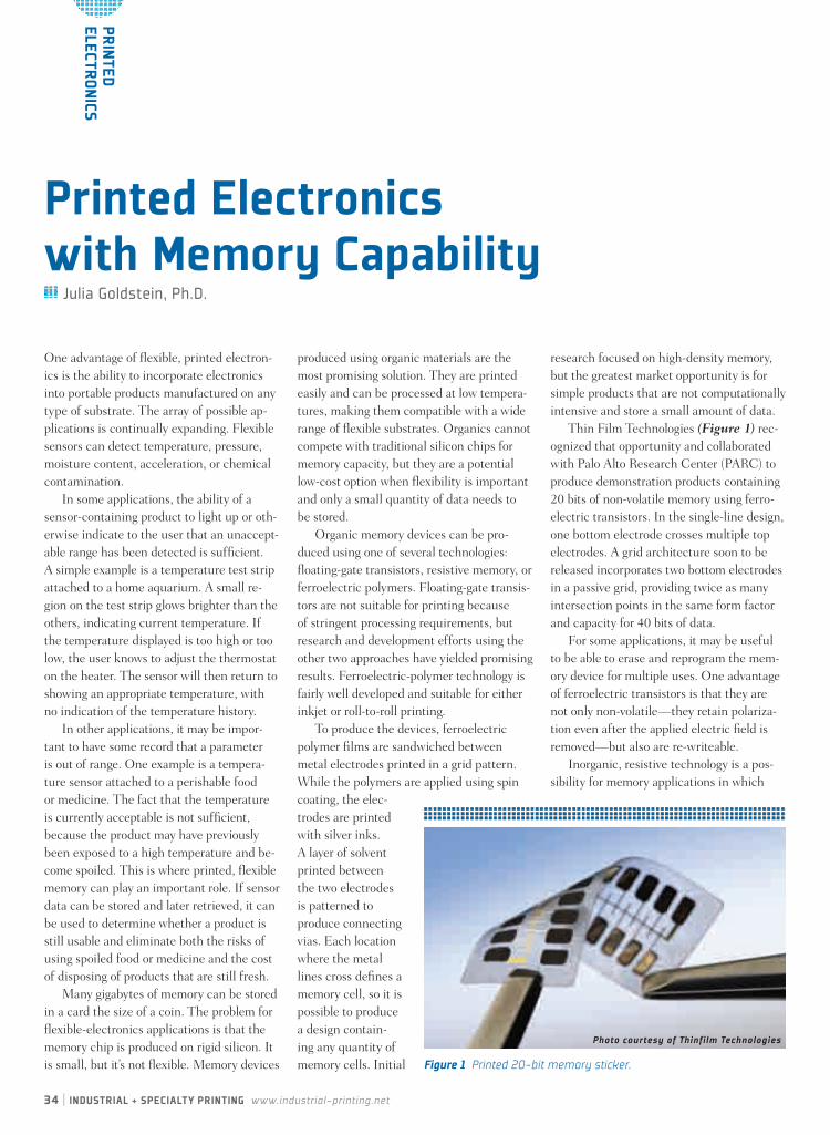
34 | IndustrIal + specIalty prIntIng www.industrial-printing.net
prInted electronIcs
printed electronics with Memory capability
One advantage of flexible, printed electron-ics is the ability to incorporate electronics into portable products manufactured on any type of substrate. The array of possible ap-plications is continually expanding. Flexible sensors can detect temperature, pressure, moisture content, acceleration, or chemical contamination.
In some applications, the ability of a sensor-containing product to light up or oth-erwise indicate to the user that an unaccept-able range has been detected is sufficient. A simple example is a temperature test strip attached to a home aquarium. A small re-gion on the test strip glows brighter than the others, indicating current temperature. If the temperature displayed is too high or too low, the user knows to adjust the thermostat on the heater. The sensor will then return to showing an appropriate temperature, with no indication of the temperature history.
In other applications, it may be impor-tant to have some record that a parameter is out of range. One example is a tempera-ture sensor attached to a perishable food or medicine. The fact that the temperature is currently acceptable is not sufficient, because the product may have previously been exposed to a high temperature and be-come spoiled. This is where printed, flexible memory can play an important role. If sensor data can be stored and later retrieved, it can be used to determine whether a product is still usable and eliminate both the risks of using spoiled food or medicine and the cost of disposing of products that are still fresh.
Many gigabytes of memory can be stored in a card the size of a coin. The problem for flexible-electronics applications is that the memory chip is produced on rigid silicon. It is small, but it’s not flexible. Memory devices
Julia Goldstein, Ph.D.
produced using organic materials are the most promising solution. They are printed easily and can be processed at low tempera-tures, making them compatible with a wide range of flexible substrates. Organics cannot compete with traditional silicon chips for memory capacity, but they are a potential low-cost option when flexibility is important and only a small quantity of data needs to be stored.
Organic memory devices can be pro-duced using one of several technologies: floating-gate transistors, resistive memory, or ferroelectric polymers. Floating-gate transis-tors are not suitable for printing because of stringent processing requirements, but research and development efforts using the other two approaches have yielded promising results. Ferroelectric-polymer technology is fairly well developed and suitable for either inkjet or roll-to-roll printing.
To produce the devices, ferroelectric polymer films are sandwiched between metal electrodes printed in a grid pattern. While the polymers are applied using spin coating, the elec-trodes are printed with silver inks. A layer of solvent printed between the two electrodes is patterned to produce connecting vias. Each location where the metal lines cross defines a memory cell, so it is possible to produce a design contain-ing any quantity of memory cells. Initial
research focused on high-density memory, but the greatest market opportunity is for simple products that are not computationally intensive and store a small amount of data.
Thin Film Technologies (Figure 1) rec-ognized that opportunity and collaborated with Palo Alto Research Center (PARC) to produce demonstration products containing 20 bits of non-volatile memory using ferro-electric transistors. In the single-line design, one bottom electrode crosses multiple top electrodes. A grid architecture soon to be released incorporates two bottom electrodes in a passive grid, providing twice as many intersection points in the same form factor and capacity for 40 bits of data.
For some applications, it may be useful to be able to erase and reprogram the mem-ory device for multiple uses. One advantage of ferroelectric transistors is that they are not only non-volatile—they retain polariza-tion even after the applied electric field is removed—but also are re-writeable.
Inorganic, resistive technology is a pos-sibility for memory applications in which
Figure 1 Printed 20-bit memory sticker.
Photo courtesy of Thinfilm Technologies

march/april 2012 | 35
re-writeability is not important. VTT Technical Research Centre of Finland has produced write-once-read-many (WORM) memory devices using conductive nanopar-ticle inks. When a voltage is applied to the circuit, the nanoparticle structure under-goes rapid sintering and exhibits a cor-responding drop in resistivity. Because the final resistance can be controlled precisely, the device can be designed as a multilevel operation to increase memory capacity. VTT produced a demonstration of this technology with electronic questionnaire cards, where a memory bit is sintered when a button on the card is pressed.
Research efforts at Mid-Sweden Uni-versity have resulted in an RFID moisture sensor with WORM memory functionality. The device, an array produced with silver nanoparticle inks printed on photo paper, exhibits a dramatic drop in resistance when exposed to 80% relative humidity. Researchers reported resistance stability during a 15-hour test, but further work is needed to demonstrate non-volatility over longer time periods.
One issue with printed memory is how to read the stored data. Several options are
available, and the choice depends on the application. VTT envisions either contact or non-contact (wireless) readout options with an external coupling to each bit of data, or memory addressing logic printed into the device. Contact pads on the surface of the memory device can be connected to an ex-ternal reader, but this may not be convenient for the customer. For example, a project incorporating memory into Pokemon cards to store character data was not marketable because users did not want to have to plug cards into an external reader.
Thin Film’s current demonstration vehicle is a handheld video game that also functions as a card reader, designed to be more convenient for the user. The memory is built into a card that is inserted into the game module and stores data on the level achieved in the game.
A sensor-plus-memory device that detects product spoilage may also work well with a reader placed in a location where perishable products are stored. A non-con-tact option for reading memory, such as a sweep-over wireless reader in the form of an electrically active barcode, would also be suited nicely to sensor applications. Readout
Julia Goldstein, Ph.D., is a freelance writer with a background in materials science. She provides commercial writing for companies in the semi-conductor and printed-electronics industries.
Julia Goldstein, ph.d.
from a sensor could be linked directly to individual bits in the bar code.
For the memory to be addressable, it is necessary to incorporate logic. In the Thin Film/PARC device, each memory cell includes one addressing and one memory transistor, allowing addressability in a fully printed device. Each cell has a separate readout line. For some applications, it may make sense to integrate printed sensors and memory with a small, thin Si chip.
The addition of printed memory, pro-duced with either ferroelectric polymers or inorganic resistive technology, holds many opportunities for the future of portable, flex-ible sensors and other products.
QUALITY RELIABILITY EXPERIENCE
Contact us today for all of your Marabu screen and pad print needs.Marabu North America Customer Service (P) 978.777.2160 (F) 978.777.7940 www.marabu-northamerica.com
A tradition of dedication to the print decorating industry.
A Proactive Partnerin Printing!
UVGL: UV screen ink for Glass, Ceramic, and Metal substrates.
No post oven baking!California Prop 65 Compliant!
TPR/TPU/TPT/TPL/TPY/TPC:Versatile solvent base and UV
pad printing inks.
NEW Marabu’s eye catching, high quality UVC screen ink for a broad range of plastic
substrates such as pre-treated polyethylene, polypropylene,
polyester and more.
Heavy Metal Free inks.
Compliant to EN-71, Part 3Safe for Toys
Medical Class VI inks.
NEW MCDµ: Fast, efficient, repeatable color match dispenser from Marabu!Used in conjunction with our standard MCM software
Test accuracy is 0.04-0.05 grams 24-station ink canister systemValves cleaned automatically after use Inks agitated in the canisters
Marabu is a Green Partner Company offering safe andenvironmentally friendly UV and solvent base inks.

36 | IndustrIal + specIalty prIntIng www.industrial-printing.net
prIntIng m
ethods
uV-led curing for Industrial printing
UV-LED curing refers to a technique that uses energy output from light-emitting di-odes (LEDs) in the ultraviolet (UV) spec-trum to treat inks, coatings, adhesives, and other UV-curable materials. The energy generated by the ultraviolet light triggers the chain reaction, resulting in polymeriza-tion of the material and the hardening (or curing) of the material.
Traditionally, mercury-based UV lamps have been used for curing, but now more energy efficient and environmentally friendly LED-based UV technology has proven a superior solution in the printing industry. LED curing technology uses semiconductor-based LEDs to project UV light when an electric current is passed through them. When an LED is forward-biased, electrons are able to recombine with electron holes within the device, thus releasing energy in the form of photons. The color of the light emitted, or corre-sponding energy of the photon, is deter-mined by the energy gap of the semicon-ductor material.
LED lamps are recognized for their lower energy consumption, longer lifetime, improved robustness, smaller form factor, and faster on/off switching. But how do they work?
uV-led curIngThere are three key components of a UV-LED curing system that, when optimized, provide an economically advantageous, high-throughput solution to the printing industry: materials (inks) that can absorb
Richa Anand, Ph.D. Phoseon Technology
energy in the UV spectrum to undergo polymerization process; LED curing lamps that provide energy in the UV spectrum of the spectrum; and a printing system in which a UV-LED lamp is integrated to cure material that passes underneath it. These elements together provide a long-term, sustainable printing method through green technology, eliminating ozone emis-sions and lowering energy consumption.
UV LEDs have a narrow spectral output centered on a specific wavelength, ±5 nm. LEDs are solid-state devices and can be built with diodes of various wave-lengths, including—but not limited to—395, 365, 385, 405, and 410 nm, unlike the broad spectrum of wavelength output by Hg-based lamps. This monochromatic dis-tribution (Figure 1) requires new chemi-cal formulations to ensure proper curing of
UV inks and coatings. Currently, the most popular wavelength is 395 nm, with 365 nm being used in specific applications.
UV-LED curing lamps consist of mul-tiple sub-components that, when combined optimally, can drive system performance. Key components of the UV LED light source can be summarized in four major categories.
LEDs Light-emitting diodes consist of semiconducting material that is doped with impurities to create a p-n junction. Charge carriers, both electrons and holes, flow into the junction from electrodes (anode and cathode) with different voltages. When an electron meets the hole, it falls into a lower energy state, resulting in release of the energy in the form of a photon (Figure 2). The wavelength of the light emitted depends on the band-gap energy of the ma-
Figure 1 Monochromatic distribution (wavelength)
MERCURY LAMP
395 LED
uVc uVB uVa VIsIBle lIght InFrared
100-280 mm 280-315 mm 315-400 mm 400-700 mm 700 - 1800 mm

MARCH/APRIL 2012 | 37
terials (dopants) forming the p-n junction. The right combination of LEDs maximizes total UV energy.
Arrays This term refers to a group-ing or clustering of individual LEDs. The number, type, and size of LEDs—includ-ing the shape of the array and the method of connecting the LEDs electrically—all impact the array. Array architecture is tar-geted for air- and/or water-cooled systems.
Optics Photons coming out of the light source are optimized by using various opti-cal layouts. Optics are used in re ecting, molding, guiding and/or shaping the UV LED emission to maximize the energy reaching the media and cure the UV inks or coatings in various applications. The use of optics has three bene ts to the user: increased ef ciency of the UV energy irra-diated on to the material; lower array-gen-erated heat; and optimum system pricing.
Temperatures UV LEDs last up to 20,000 hours and beyond if they are maintained at proper operating tempera-tures. As LEDs emit more energy, they also generate more heat, which needs to be managed. Thermal management removes excess heat from the system while provid-ing a consistent operating temperature for the diodes to function at maximum performance.
INK FORMULATIONS AND MATERIALSWith advancements in the availability of UV-LED-optimized ink chemistry, UV LED sources have become a very viable curing solution for many in the industrial printing industry. Materials suppliers have noted the bene ts of UV-LED curing (Table 1) in general and have responded to the demand and challenge in the printing world to formulate raw materials that absorb energy corresponding to the output wavelengths of LED-based UV curing units. Industrial screen printers, for example, have found that advancements in LED-lamp technology and UV-curable ink formulations make UV-LED curing a viable alternative to medium-pressure mercury lamps. Additionally, high-power, scalable, UV-LED curing systems are effective high-speed curing in screen print-ing applications.
One of the key ingredients in the
Richa Anand, Ph.D., is product-marketing manager at Phoseon Technology, Hillsboro, OR.
RICHA ANAND, PH.D.Phoseon Technology
chemical formulation is a photoinitiator that serves as a catalyst to start the polym-erization process when exposed to narrow spectrum UV LED energy. And with the continued, widespread acceptance of UV LED systems, availability of suitable base materials continues to grow. The driving factors in advancement of chemistry of raw materials is increased capability and cost effectiveness of commercially available UV-LED curing lamps.
APPLICATIONS IN INDUSTRIAL PRINTING AND DECORATINGUV-LED curing allows the printing industry to explore new and challenging applications. The following represent just a few examples.
Medical labeling The pharmaceuti-cal industry demands exacting product development and production in a sterile and clean environment. The industry has continued to push the envelope of what is possible; enabling new advances in medicine. UV-LED technology brings inherent advantages to the world of print-ing, including the lack of IR radiation in heat-sensitive applications in cleanroom conditions.
Bottle printing Today, UV-LED cur-ing technology is integrated in printing units for a variety of label applications, including bottle-labeling machines and systems designed for direct printing on cylindrical beverage containers. The small size of the light sources makes them ideal for machines with limited space. It also allows for printing on heat-sensitive sub-strates without damaging the materials. These solutions enable users to process a variety of materials at maximum produc-tion speeds, with a fraction of the power requirements of a typical arc lamp.
Printed electronics and photovoltaicsMass-produced consumer electronics and tight-tolerance photovoltaics applications bene t from the long life, reliability, and repeatability of UV-LED curing systems. The ability to function at optimum levels, even during long-lasting, high-volume jobs—and provide consistent output when curing very sensitive products—makes UV-LED technology an effective solution in these markets.
CONCLUSIONUV-LED curing is now an accepted tool in the printing industry. It opens challeng-ing applications to industrial printers who specialize in a variety of imaging processes and push the formulation of advanced inks, coatings, and other consumables. At the same time, UV-LED curing units have become more ef cient in delivering higher energy to the media, driving the engineer-ing and implementation of environmentally clean, energy ef cient, and compact curing units that increase throughput and sup-port exibility in a variety of production environments.
Figure 2 An example of a p-n junction as it applies to LED emissions
Forward Bias
JunctionN Type P Type
Photon emitted
Table 1 Benefi ts of UV-LED curing
BENEFIT FEATUREECONOMIC • Energy Effi cient
• Long Lifetime• Low Maintenence• Low Operating Temperatures
ENVIRONMENTAL • Mercury Free• Ozone Free• Workplace Safety• UV-A Wavelegnth
ADVANCED CAPABILITIES
• Heat Sensitive Substrates• Deep, rough Cure• Small, Compact Machines• Controlled Curing Intensity

38 | IndustrIal + specIalty prIntIng www.industrial-printing.net
Industry InsIder
The role of printing in pervasive electronics
The application of printing techniques to electronic devices has come a long way. Until about 1990, attempts to make semi-conductor devices with printable materials had met little success. The discovery by Richard Friend and colleagues at Cambridge University of polymer light-emitting diodes in 1991, however, led to an explosion of activity in the synthesis of soluble semi-conducting organic materials. In the same period, well-controlled procedures emerged for the preparation of inorganic nanocrystals in sufficient quantities for making active devices and conducting lines. Thereafter, researchers applied inkjet printing to fabri-cation of these devices, and it was quickly observed that conventional graphics printing techniques such as offset, gravure, etc., were potentially much faster.
During this time, in parallel with the development of the Internet into a truly world-wide network, the vision articulated by the Auto-ID Labs at MIT of a global electronic identification system for objects of commerce evolved into the modern vision of the Internet of Things, in which every object is interconnected, and many of them have some awareness of their environment (i.e. sensors). However, realizing this vision clearly required far cheaper electronics than almost any self-standing units previ-ously known; the target for simple, passive, RFID tags became $0.05 or less, including antennae. Using roll-to-roll printing, with the prospect of high throughput and low per-unit capital cost to make these products, attracted keen interest.
Thus, we see several motive threads intermingled: printing, flexibility, large area, inexpensive, and pervasive. These share some common features but comprise distinct attributes. Printing can be done
Jayna Sheats, Ph.D. TerePac
on rigid substrates also, and First Solar has proven persuasively that inexpensive, thin-film semiconductor products can be made (with vacuum processes) on rigid, large substrates. Most important, however, is the pervasive quality. A huge range of applica-tions are commonly mentioned, such as medical, traffic, and chemical-flow sensors, food-freshness sensors, lab-on-a-chip, and intelligent packaging. Actual electronic re-quirements for these applications will differ substantially.
High clock speed, vital for most consum-er electronics, is not of great value for these distributed wireless sensors. However, low-power consumption is absolutely paramount to avoid changing billions of batteries every few months; state-of-the-art energy harvest-ing limits device currents to the microamp regime with a small active duty cycle—most of the time spent dormant, at nanoamp or lower levels. At the same time, functions such as high data quality (no errors), strong security, and ease cannot be neglected.
Texas Instruments (TI) introduced a product named SimpleLink, targeted to the Internet of Things, while ST Microelectron-ics has its GreenNet. The TI product has 6 kB of flash and 3 kB of RAM; GreenNet contains a 32-bit microcontroller and 2.4 GHz radio, along with autonomous power source. While these no doubt represent ap-proaches that are not optimized for specific applications, they do give an indication of the kind of content that current customers are expecting, and are typical of units being offered by many companies for this purpose. Any printing approach to fabrication has to be prepared to provide solutions at this scale of complexity.
The significance of Moore’s Law arises from the amenability of the logic transistor
to nearly indefinite shrinkage without loss of performance. Printing, developed with the human eye in mind, resolves spots at best a thousand times larger than ULSI microlithography. Because processing cost of planar devices is proportional to area, ones with smaller features are strongly favored to win despite higher patterning-equipment costs. Techniques are now avail-able for placing ultra-thin and tiny, inexpen-sive, silicon ICs into flexible packages.
Where the product is intrinsically large area, with no high-resolution patterning, printing is most effective, and so should be expected to realize its greatest value in solar cells; companies such as Nanosolar, Solexant, and Konarka are demonstrating this now. Displays occupy an intermediate position. Pixels are matched to printing reso-lution, although requiring greater precision than conventional graphics. Backplane tran-sistors must be smaller than the pixels, but there is no advantage in shrinkage to sub-micron dimensions; hence, the competition between printing and traditional lithograph-ic processing for this application. For the circuits used by the Internet of Things, thin silicon will likely prevail. Printed interdevice interconnects, however, are essential. The integration of multiple printing techniques and nontraditional silicon assembly in an ef-fective physical package will keep innovators busy for some time.
Jayna Sheats, Ph.D. is president and CEO of TerePac.
Jayna sheatsTerePac

SOURCE:
WHAT WE MAKE IS CLEARLY CONDUCTIVE, WHAT WE DO IS A LOT MORE
The ORGACONTM product line consists of coating solutions, screen- and inkjet printing inks for manufacturing transparent flexible elec-trodes for Electroluminescent lamps, Display devices, Capacitive Touch sensors, Organic Photovoltaics, and other Printed Electronics applications. Based on a water dispersible form of the intrinsic conductive polymer PEDOT, made and applied by Agfa for over 20 years now in the permanent antistatic treatment of polyester films.
ORGACON products show a unique combination of high transpar-ency, conductivity, flexibility and processability that is not matched by other organic or inorganic conductive based-materials.
www.agfa.com/orgacon
A Paid Advertising service of ISP magazine.
ADVERTISING INDEXMarch/April 2012
Advertiser page Advertiser page
AGFA 39 Marabu North America 35
AGL 29 Mimaki USA OBC
AWT World Trade Inc. 23 Novacentrix IFC
Douthitt Corp. 3 Ohio Gravure 5
Dynamesh Inc. 9 RH Solutions 5
Graphic Parts International 23 Schober Technologies GMB 29
Industrial-Printing.net 21 Spartanics 23
Kammann USA Inc. 7 SGIA IBC
Lintec of America 39 Xenon Corporation 7
MacDermid Autotype 1

40 | IndustrIal + specIalty prIntIng www.industrial-printing.net
shop tour
Automated screen-printing press
Laser cutting
RSP owners and management team
rsp, Inc.LocAtion Milwaukee, WiotheR info RSP was founded 50 years ago as Ryan Screen Printing, inc. it remains a family-owned op-eration, third generation, that manufactures membrane switches and control panels. The company offers contract manufacturing services, engineering, design, screen printing, digital printing, and assembly from its Milwaukee-based headquarters. The graphic-overlay and membrane-switch group in Milwaukee has a long history of experience in this area. RSP also does rubber molding, plastic molding, touch screens, and wire harnesses. in 2009, the company established RSP electronics in PingDi, china to handle rubber and plastic molding, screen printing, and assembly production.
1 The screen-printing line
Screen printing on silicone keypads
close-up view of a press operator in action
2
3
4
5
6
2
1
3
4
5
6

Sign up to be notifi ed when registration opens:registration opens:
SGIA.orgregistration opens:registration opens:
Keyword:Expo2012
c12_ad1_iSP.indd 1 2/23/12 5:33 PM

Flex your UV optionsUV LED TABLETOP FLATBED PRINTER
Expand your UV
industrial printing
in new directions
with the UJF-3042FX
and its new flexible
ink sets and primer
ink for printing on
practically anything.
C M Y K lc lm + W + Cl
C M Y K + W + Cl
C M Y K + W C M Y K lc lm + W + Cl
C M Y K + W + Cl
C M Y K + W
C M Y K lc lm + W + Cl
C M Y K + W + Cl
C M Y K + W
INKSUBDYEUJF-3042FX Expanded Ink Sets
Mimaki’s tabletop-sized UJF-3042FX is a versatile and affordable UV LED flatbed printer with a generous print area of 11.8” x 16.5” for printing on a growing choice of substrates and dimensional objects up to 1.9” thick. Now with the addition of our new Primer and Flexible inks for optimaladhesion, your substrate choices open up to plastics, metals, glass and more.
ATL 888-530-3988 BOS 888-530-3986 CHI 888-530-3985 LA 888-530-3987www.mimakiusa.com
EMAIL INFO [email protected]
© 2012 Mimaki USA, Inc.
Use the UJF-3042FX for: one-offs, prototypes, industrial and interior signage, molded switches and panels, packaging, ID badges, promotional items. You’ll find the application options are more flexible than ever.
PR-100 is a NEW UV Primer ink that can be used in combination with LF-140 and LF-100 inks. This primer ink is simultaneously under-printed as a spot ink with CMYK.
LF-140 is a NEW UV Flexible ink offering 6-color print-ing along with white and clear. More flexible than LH-100 ink, making it less likely to crack during post-processing.
LF-200 is a NEW UV Ultra-Flexible ink that is able to stretch up to 200% without cracking.
LH-100 is a UV Hard ink that excels in scratch and chemical resistance and is ideal for media that does not require bending or folding after printing.
Scan to see UJF-3042FX applications. or go to: www.mimakiusa.com/qr-ads/121511/UJF3042FX/apps/
See the UJF-3042FX and more . . .Booth 1944 | Orlando, March 22-24
Mimaki 3042FX_FBC_ISP0112.indd 1 2/17/12 5:09 PM