inculcation of simultaneous clock gating and power gating ....pdf · “sleep” transistor is...
TRANSCRIPT

International Journal of Science and Research (IJSR) ISSN (Online): 2319-7064
Impact Factor (2012): 3.358
Volume 3 Issue 8, August 2014 www.ijsr.net
Licensed Under Creative Commons Attribution CC BY
Inculcation of Simultaneous Clock Gating and Power Gating in Sequential Design
Vivek Dadheech1, Ghanshyam Jangid2
1M.Tech student, Department of ECE, Gyan Vihar School of Engineering and Technology, SGVU, Jaipur, Rajasthan, India 2Assistant Professor, Department of ECE, Gyan Vihar School of Engineering and Technology, SGVU, Jaipur, Rajasthan, India
Abstract: This paper presents simultaneous use of clock gating and power gating in a sequential circuit, we have taken True Single Phase Clock (TSPC) FF. Clock gating is use to reduce the dynamic power whereas power gating technique is the best way to minimize the leakage current. If both the technique use in single circuit then we can minimize the power consumption and increase the performance of the circuit which also reduce the cost of the circuit, as also cost depends on the power consumption. Keywords: Clock gating, Power gating, TSPC FF, Sequential circuit.
1. Introduction As we know that VLSI is depend on the three major factors which is power, cost and speed. Power consumption is the vast issue in the present era and every new design is made to reduce the power. If power get reduce then the cost automatically get reduce and performance of the circuit increases. We are working on sequential circuits to minimize the power by applying clock gating and power gating technique in a single sequential circuit. Clock gating technique uses a gated clock pulse which is feed in the desire circuit. We use AND gate for gated clock signal. Instead of applying clock pulse we apply pulse to the AND gate with the enable signal, when both the inputs are “high” only then the out goes “high”. Hence the gated clock gives output high only in one condition and we can reduce the dynamic power using this technique. Power gating technique is use to reduce leakage current to some extent. In power gating we use sleep transistors, which is used to reduce the leakage current at pull down network. By applying fine-grain power gating approach, a “sleep” transistor is added to each and every cell, although the power of each cluster of cells is gated individually. Power gating is a modern technique that uses “sleep” transistors as high Vt devices to disconnect low Vt logic cells from the supply or ground to reduce the leakage in the sleep mode. In this paper we will discuss two sections, first we will discuss about the previous work clock gating and power gating technique in section 2, and then we will discuss the proposed work under section 3 in which we will use both the technique in a sequential TSPC FF. 2. Previous Work In previous work [1][2] we can notice that clock gating and power gating used in a single circuit, drawbacks and limitation of combining both the technique has been discussed, clock gating gives solution of circuit testability, formal verification and time closure. In power gating sleep transistor driven by the same sleep signal. This technique is best on large circuits, sleep transistors can control
clusters presents in gates. The three major problem clustering, size of ST and design of circuitry has been resolved to integrate both CG and PG in a single circuit.
Figure 1: Integration of CG and PG
Combining CG and PG [1] is convenient when the energy necessary to reactivate the circuit is smaller than the leakage energy consumed by the circuit in the idle state. CG is done via open database. Pulse applies directly to the design and also checks the simulation of the design with CG. This is the total technique which needed to setup the design and then if above steps would be done successfully then only add sleep transistor which is PG process. Low power design using CMOS based on T-SPICE simulator [3] in which enumerates low power. MTCMOS has been proposed which is based on DFF. As we discussed in the first paper that an extra NMOS is add in the TSPC FF which changes its functionality to low power design. As we are aware that in electronics devices Flip-Flops are the best source to stores the logical state of one or more than one data input signal. During the rise and fall signal data stored in a set of Flip-Flop present currently due to which we can feed it as an input to the other sequential circuit. Double edge triggered Flip Flops stores the data on both the edges. 3. Proposed Work 3.1) Sequential TSPC FF Low power design TSPC FF is modify version of D FF, the circuit consists of dual TSPC FF, we can say it is a sequential TSPC FF in which the output of first is the input of the second stage. Our aim is to reduce the power
Paper ID: 02015493 757

coin
3Cclpu
WH 3Athondespdu
Geq 3Wthse
onsumption (nitial input for
F
.2) ClockCG is AND glock and the ulse to reg_A
When both EnHence dynamic
.3) PowerAn additional she pull downnly when ievices are usupurious transiue to mismatc
Glitches can bqualise gates p
.4) SequeWe use CG anhe circuit withequential desi
(dynamic +ler the circuit.
Figure 2: Seq
k Gating gate with twooutput is gatinstead of “cl
Figure 3:
n and clock arc power get re
r Gating sleep transisto
n network. Lainterconnect ually optimal fitions, gates ch in path leng
Figure 4: P
be eliminated path lengths o
ential circuit nd PG in TSPChout CG and ign of TSPC F
Internatio
Licens
eakage) powe
quential TSPC
o input signaled clock whilock”.
Clock Gating
re “1” then gaeduce.
or is added toarger sized dedominated.
for low-powehave nonzero
gths of circuit
Power Gating
using insertior we can rede
with CG andC FF and then
PG techniquFF, in which
onal JournaISSN
Impac
Volume 3
sed Under Cre
er. D and clk
FF
l named ENich is input c
ated clock is
o the pull up oevices are usMinimum sr. Glitches cauo delay, Glitc.
g
ion of bufferesign the circu
d PG n compare it fue. It is a dua
AND gate is
al of SciencN (Online): 23ct Factor (201
3 Issue 8, Awww.ijsr.ne
eative Commo
k is
and lock
“1”.
or to seful ized uses ches
rs to uit.
from al or use
to1p
Tdvep
TpotoAinwin
F
Hwtrthrm
4
Icp
ce and Rese19-7064
12): 3.358
August 2014et ons Attribution
o provide gate1 TSPC and thpulse to the se
TSPC FF condown circuitryvoltage sourceend tool to sipower and vol
The proposedprovide Clk aoutput of ANDo the stage 1
After that outpnput of seco
which generatenput to the sec
Figure 5: Sch
Hence by applwe can minimransistors usehe glitch or
resolve the iminimizes pow
4. Result a
n this paper wcircuit, if wepossible to red
earch (IJSR
4
n CC BY
ed clock signahe second ANcond stage TS
nsists of 5 tray use to minie is provided imulate the dltage of each s
circuit consisand D as an D gate which iTSPC with D
put of stage 1 nd AND gate Clk2 as an ocond stage TS
hematic diagraCG
lying clock gamize dynamicd in pull downminimize thessue of leakwer consumpt
and Compa
we used CG andid not use
duce the powe
R)
al as an input D gate provid
SPC FF.
ansistors, the imize the leak
to the circuidesign. The wstage.
sts of 28 transinput in AN
is Clk1 becomD. Clk1 works
which is Out1te and the seoutput. Clk2 iSPC FF.
am of Sequentand PG
ating techniqu power. Nown network reme leakage to
kage power. ion up to 20-3
arison
nd PG techniq this techniq
er consumption
clock of the sdes the gated c
3 additionalkage power. 2itry. We usewave form sh
istors, initiallyND gate, thenme one of the is as a gated cl1 fed as one oecond AND s fed as one o
tial TSPC FF w
e in both the sw the additionmove or elimin
some extentWhich techn
30%.
que in a sequeque than it isn to that level
stage clock
pull 2.5V back hows
y we n the input lock.
of the gate,
of the
with
stage nal 3 nates
and nique
ential s not .
Paper ID: 02015493 758
Hbe7se
S
5 Inloanonfosowu Wcaisciciupotrsi
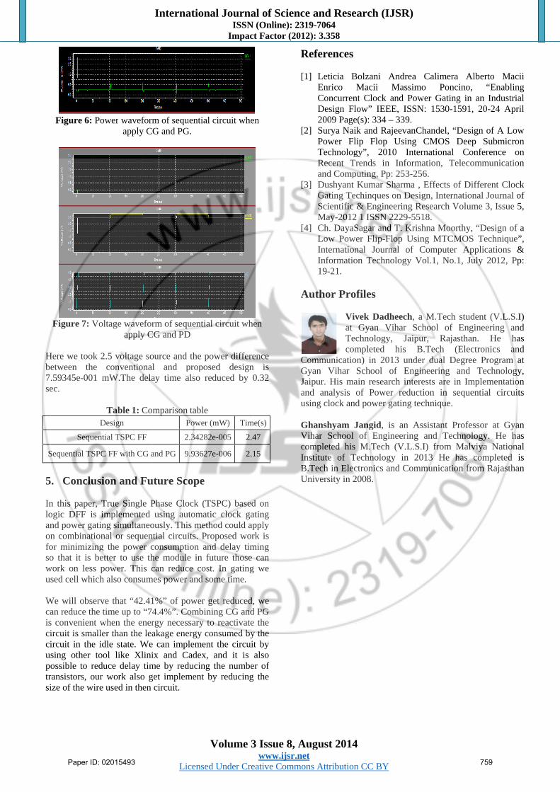
Figure 6: Po
Figure 7: Vo
Here we took 2etween the .59345e-001 ec.
D
Sequen
Sequential TSPC
5. Conclus
n this paper, ogic DFF is ind power gatin combinationor minimizingo that it is be
work on less psed cell which
We will observan reduce the s convenient wircuit is smallircuit in the ising other toossible to redransistors, ourize of the wire
ower waveforapply C
oltage waveforapply C
2.5 voltage soconventiona
mW.The dela
Table 1: CoDesign
ntial TSPC FF
C FF with CG a
ion and Fu
True Single Pimplemented ing simultaneonal or sequeng the power cetter to use thpower. This ch also consum
ve that “42.41time up to “7
when the enerler than the leidle state. Weool like Xliniduce delay timr work also ge used in then
Internatio
Licens
rm of sequentiCG and PG.
rm of sequentCG and PD
ource and the al and propay time also
omparison tablPowe
2.342
and PG 9.936
uture Scope
Phase Clock (using autom
ously. This mential circuits. Pconsumption he module in can reduce co
mes power and
1%” of power4.4%”. Combrgy necessaryakage energy
e can implemeix and Cadexme by reducinget implement
circuit.
onal JournaISSN
Impac
Volume 3
sed Under Cre
ial circuit whe
tial circuit wh
power differeposed design
reduced by 0
le er (mW) Tim
282e-005 2.4
627e-006 2.
e
(TSPC) basedmatic clock ga
ethod could apProposed worand delay timfuture those
ost. In gatingd some time.
r get reduced,bining CG andy to reactivate
consumed byent the circuix, and it isng the numbet by reducing
al of SciencN (Online): 23ct Factor (201
3 Issue 8, Awww.ijsr.ne
eative Commo
en
en
ence n is 0.32
me(s)
47
15
d on ating pply rk is ming
can g we
, we d PG e the y the it by also
er of g the
R
[
[
[
[
A
CGJau
GVcIBU
ce and Rese19-7064
12): 3.358
August 2014et ons Attribution
References
1] Leticia BEnricoConcurrenDesign Fl2009 Page
2] Surya NaiPower FlTechnologRecent Tand Comp
3] DushyantGating TeScientificMay-2012
4] Ch. DayaSLow PowInternationInformatio19-21.
Author Pro
ViatTeco
CommunicatioGyan ViharJaipur. His maand analysisusing clock an
Ghanshyam JVihar Schoolcompleted hisnstitute of T
B.Tech in ElecUniversity in 2
earch (IJSR
4
n CC BY
Bolzani AndrMacii Mas
nt Clock and low” IEEE, Ie(s): 334 – 33ik and Rajeevlip Flop Usigy”, 2010
Trends in Infputing, Pp: 25
Kumar Sharmechinques on D
& Engineerin2 1 ISSN 2229Sagar and T.
wer Flip-Flop nal Journal on Technolog
ofiles
ivek DadheecGyan Vihar
echnology, Jmpleted his
on) in 2013 uSchool of E
ain research iof Power re
nd power gatin
Jangid, is anof Engineer
s M.Tech (V.Technology inctronics and C2008.
R)
rea Calimerassimo PoncPower Gatin
ISSN: 1530-19.
vanChandel, “ing CMOS International
formation, Te3-256. ma , Effects oDesign, Internng Research V9-5518. Krishna MooUsing MTCMof Computer
gy Vol.1, No.
ch, a M.Techr School of Jaipur, Rajas B.Tech (under dual DEngineering interests are ieduction in sng technique.
n Assistant Pring and Tec.L.S.I) from n 2013 He hCommunicatio
a Alberto Mcino, “Enab
ng in an Indus1591, 20-24 A
“Design of ADeep Submi
Conferenceelecommunica
of Different Cnational JournVolume 3, Issu
rthy, “DesignMOS Techniqr Application.1, July 2012,
student (V.LEngineering
asthan. He(Electronics
Degree Programand Technol
in Implementasequential cir
Professor at Gchnology. HeMalviya Natihas completeon from Rajas
Macii bling strial April
Low icron
on ation
Clock nal of ue 5,
n of a que”, ns & , Pp:
L.S.I) and has and
m at logy, ation rcuits
Gyan has ional ed is sthan
Paper ID: 02015493 759