in this issue: - nist page
TRANSCRIPT

In This Issue:
A rticles
Calibration of Beta-ParticleOphthalmic Applicators at theNational Bureau of Standards J. S. Pruitt 165
Room TemperatureGold-Vacuum-Gold Tunneling Experiments E. Clayton Teague 171
Conference Reports
Conference onPrecision Electromagnetic Measurements Norman B. Belecki 235
Technical News Briefs
New Technical Developments 237
New Services From NBS 240
New Standard Reference Materials 241

Journal of Research of the National Bureau of Standards
Calibration of Beta-ParticleOphthalmic Applicators at theNational Bureau of Standards
July-August 1986
J. S. Pruitt
National Bureau of StandardsGaithersburg, MD 20899
The method used at the National Bu-reau of Standards for the calibration ofstrontium-90 + yttrium-90 beta-particleophthalmic applicators in terms of ab-sorbed dose to water, is described, Themethod involves measurement of ioniza-tion density at the applicator surfacewith an extrapolation chamber, correc-tion for the difference in backscatter be-tween the collection electrode andwater, and application of the Bragg-
Gray equation. The calibration obtainedis an average over the active surface ofthe applicator. The overall uncertaintyof the surface calibration is about ± 15percent.
Key words: absorbed dose; calibrationservice; electron dosimetry; ophthalmicapplicator; surface dose.
Accepted: August 27, 1986
1. Introduction
This paper describes the calibration of strontium-90 + yttrium-90 beta-particle ophthalmic applica-tors in terms of absorbed-dose rate to water at thesurface of the applicator. The calibration is madewith an extrapolation ionization chamber, an in-strument invented by Failla [l]' which has sincebeen shown by several investigators [2,3] to be par-ticularly well suited to the determination of ab-sorbed-dose rate for beta-particle sources. Thetechniques of measurement have been sufficientlyrefined to permit the successful international com-parison of several sources at distances of 20 and 30cm, to within one percent [4].
For ophthalmic applicators, the quantity of inter-est is absorbed-dose rate at the applicator surface.
About the Author: J. S. Pruitt is with NBS' Ioniz-ing Radiation Division, Center for Radiation Re-search.
The problems introduced by reducing the sourcedistance from 20 cm to zero make calibration un-certainties of about 15 percent realistic. Within thislimit, it has been found that a reliable surface cali-bration of an ophthalmic applicator can be ob-tained with an extrapolation chamber. Theextrapolation chamber technique has been used atthe National Bureau of Standards (NBS) since 1977to calibrate about 10 ophthalmic applicators peryear. Alternative methods, using thermolumines-cent dosimeters (TLD) have also been described[5]. The use of TLD's offers a simpler and less elab-orate approach, but it requires calibration of theTLD material in another radiation source, and wasnot considered an appropriate method for use atNBS.
The general plan of the calibration is to measureionization current per unit mass of air with the ap-plicator at several distances from the center of theextrapolation chamber air gap, and to extrapolate
165
Volume 91 Number 4
' Figures in brackets indicate literature references.

Journal of Research of the National Bureau of Standards
to zero distance to obtain a value at the surface ofthe applicator. The following three sections areconcerned with this determination of extrapolatedcurrent per unit mass of air. This is followed by asection describing the calculation of the absorbed-dose rate, and a final section about the errors inher-ent in this calibration method.
2. The Extrapolation Chamber
The extrapolation chamber is essentially thesame as that described by Loevinger and Trott [6],with several collecting electrodes which can be in-terchanged and a thin aluminized-plastic-film high-voltage electrode. The electrode spacing can bechanged by rotating the high-voltage-electrodesupport, at the rate of 0.635 mm per revolution.The relative position of the electrodes and an oph-thalmic applicator under study are shown in figure1. The particular collecting electrode shown has adiameter of 28 mm and is surrounded by a guardelectrode with an outside diameter of 50 mm. Bothguard and collecting electrodes are made of 8 mmthick A-150 conducting plastic, electrically isolatedwith 30-pim plastic film held in place with epoxycement. The high-voltage electrode is aluminizedplastic with a diameter of 80 mm and a thickness of0.7 mg/cm 2 .
The collecting electrode shown in figure 1 has amuch larger area than the active area of all ordi-nary ophthalmic applicators. This type of collect-
BRASS BACKING
-GUARD ELECTRODE7 COLLECTING ELECTRODE
\ COAXIAL CONNECTOR
l INSULATING FILMS
t UZHIGH VOLTAGE ELECTRODE
OPHTHALMIC APPLICATOR
Li
.X
Figure 1-Schematic diagram of ophthalmic applicator and crosssection of extrapolation chamber electrodes.
ing electrode is used to determine the ratio (1/d)o,where I is the ionization current generated in theair volume defined by the collecting area, A, andthe electrode separation, d. The ratio I/d is a func-tion of both d and the applicator distance, z, andthe zero subscript refers to the limiting case whereboth d and z are zero. This limiting value of lid isa characteristic of the source and of the electrodematerial and is independent of A, if A is sufficientlylarge.
A probe electrode of smaller area is used to in-vestigate the variations in dose rate across the sur-face of applicators. This probe is similar to the unitshown in figure 1, but the diameter of the collect-ing electrode is only 0.6 mm, and both collectorand guard are made of graphite. A 0.4 mm thickring of epoxy between collector and guard resultsin an effective probe diameter of about I mm. Withthis probe, both the local activity variation and theeffective source area are investigated by changingthe x and y coordinates of the applicator (fig. 1),for small but fixed values of z and d. The applicatorstand rests on a microscope stage to permit accu-rate variation of both x and y. Accurate adjustmentof z is made with a barrel micrometer.
Extrapolation chamber currents include contri-butions from (1) ions generated in the collectingvolume of the chamber, (2) electrons coming torest in the collecting electrode, and (3) back-ground. The first of these is the desired quantity. Itis separated from (2) and (3) by measuring both 1+with positive high voltage (a positive number) and1- with negative high voltage (a negative number).Since only (1) changes sign with the high voltage,the ion current is (I+- -)/2, a quantity which isproportional to the electrode separation, to a firstapproximation. The quantity (I+ + I-)/2, called the"parasitic" current by Hillion et al., [7] includescontributions (2) and (3) and is almost independentof electrode separation for a given applicator dis-tance.
Figure 2 shows the variation of both the ion andparasitic currents across the face of the most asym-metric applicator that has been studied in this labo-ratory. The measurements were made with theprobe electrode, using an electrode spacing of 0.05mm and an applicator distance of 0.4 mm.2 Theasymmetry of the ion current is presumably causedby an uneven distribution of activity across the ap-plicator face. The tails of the ion current distribu-tion are caused by beta rays that leave theapplicator with large velocity components perpen-dicular to the beam direction. The tails rapidly be-
2 In measurements made with the 28 mm collecdng electrode,the parasitic current is only 5-lo percent of the ion current.
166

Journal of Research of the National Bureau of Standards
Ct
DISTANCE ACROSS SOURCE, mm
The source area is taken to be the area within thelocus of half-maximum-current points on such amap. It is determined from a plot of the measuredcurrent as a function of radius from the center ofthe distribution, as shown in figure 3 for a particu-lar applicator. For most applicators, the current de-creases monotonically with increasing radius.? A 50percent radius, R, can be read directly from thegraph, and the area calculated from this as 7rR2.This is a close approximation to the real area, 7rR',if the chamber spacing, d, and source distance, z,are both sufficiently small. A rough estimate of un-certainty for a given d and z can be obtained fromthe following equation describing the ionizationcurrent per unit volume as a function of position:
dlTV = K - loge
Figure 2-Variation of ion current andapplicator SN 0136.
parasitic current across
come more prominent as the applicator distance zincreases.
The graph of parasitic current in figure 2 showsevidence both of electrons coming to rest in thecollecting electrode (the central peak of the distri-bution), and background (the negative tails). Thecentral peak of the parasitic current is more sym-metrical than the ion current peak, probably be-cause of multiple scattering of the primary beam inthe collecting and guard electrodes, which tends toround off the edges of the distribution. The back-ground is a leakage current of about 10-50 fA. It isunaffected by high-voltage polarity changes, asstated earlier. The parasitic currents are generallyignored.
Initial inspection of an applicator is made withthe probe electrode, using as small an electrodeseparation and applicator distance as can be toler-ated. The applicator face is mapped at points sepa-rated by 2 mm, over a grid of sufficient extent forthe ion current to drop below half of its maximumvalue along all tracks. This crude map permits cal-culation of the source area and provides a qualita-tive picture of the source symmetry and activitydistribution. On occasion, when more detail is re-quired or when the source diameter is found to beonly a few millimeters, a I mm or even a 0.5 mmgrid spacing is used.
'For some applicators, the probe electrode map shows re-gions of high activity near the edge of the distribution. Thesehot spots make the determination of area very uncertain and atthe same time bring the medical use into question. We decline tocalibrate such sources and recommend against their use as oph-thalmic applicators.
3.0 .1
2.0US0Zj
< 1.5N
0
0.5
00 2 4 6 8
RAD US, mm
Figure 3-Currents measured with the probe electrode across theface of SN D-402, plotted as a function of radius, measuredfrom the center of the current distribution. The curve wasdrawn freehand.
167
3. Determination of Source AreaIn0

Journal of Research of the National Bureau of Standards
[ I~~~~~q +77 pZ+12N_2+X+2Y2
where in terms of the coordinates of figure 1,Ip=r/R, ij=z/R, r=Vx 2+y, and K is a constant.
This equation was derived assuming that the ac-tivity is uniformly spread over a circle of radius Ron the source surface, that the beta-particles areemitted isotropically from the source surface, thattheir paths are straight, and that energy depositionis uniform along these paths. The derivation isbased on a l/r 2 distance variation and consequentlycurrent per unit volume becomes infinite as the dis-tance approaches zero. If the current/volume isnormalized to its value on the central axis of thesource (@=0), the normalized current is well be-haved for all distances (that is, for all values of 77).
Figure 4 is a plot of the normalized currents forseveral values of 7,. For each curve, the apparentradius, R, is the product of the true radius, R, andthe value of ,a where the curve crosses the half-value line. For i7=i, z=R, and I-R2 exceeds 7rR'by a factor of about 2. For 7 7=0.2 (not shown) 7rR2
exceeds 7rR2 by about 4 percent, and for 17=0.1,the discrepancy is less than I percent. In a typicalcase, d=0.2 mm, z=0.12 mm, R=4 mm, and77=0.03, for which qrR 2/7rR2= 1.001.
Figure 5 is a plot of probe ion current vs. radiusfor two applicators and matching source profilescalculated from eq (1). The parameter z was as-signed the approximate value 0.1 mm in the calcu-lation, and values of R=3.18 and 4.35 mm wereread from the graph. All four curves have been
1.0
77=1
0.5 _
* 0 I I 0 | X
F S ,~~~~~~S 0252 8
NI~~~~~D0.5 -
0
0 2 4 6RADIUS r, mm
Figure 5-Measured probe profiles of applicators SN 0258 andSN 157, in comparison with theoretical predictions foruniformly distributed sources.
normalized at the origin. Equation (1) is not an ac-curate description of either source profile, but thecomparison with SN 0258 is consistent with theassumption that the activity in this source is spreaduniformly over an area of 4.35-mm radius. Thesmall differences between theory and measurementappear to be easily explained. The differences nearr=R can be attributed to the finite size of the probeelectrode. The differences at larger radii probablyarise from the fact that the activity in SN 0258 liesbelow the applicator face, so that the elementalsources cannot be treated as isotropic at large an-gles. This will cause the real distribution to fall offmore rapidly at large radii than the theoretical dis-
Figure 4-Theoretical probe profflesfor five different source distances,\1 = z/R.
0 0.5 1 1.5 2
RELATIVE RADIUS [L= r/ R
168
I-_2Li.0:0:
CCwUN
24C2

Journal of Research of the National Bureau of Standards
tribution. The activity in SN 157, in contrast, ap-pears to be highly peaked at the center. 4
4. Determination of Average CurrentPer Unit Mass of Air
After mapping the source and measuring its area,the probe electrode must be replaced by the largercollecting electrode to determine the current perunit electrode spacing (I/d)0 . This is determined bymeasuring current, I, for five different air-gaps,d=0.5, 1, 1.5, 2, 2.5 mm, with the source distancez=d/2 in each case. These measured currents arecorrected (I) to a reference air temperature andpressure, 22 'C and 101.3 kPa; (2) for ion recombi-nation and diffusion, using the formulas and con-stants summarized by WBhm [8]; and (3) errors inthe extrapolation technique, discussed below.5 Thecorrected current is a non-linear function of d, be-cause of poor geometry, and extrapolation to zerod is imprecise. The corrected current is fitted to acubic equation in d constrained to pass through theorigin. The ratio l/d is then a quadratic functionthat can be written:
I Q)(t +ad i jd2). (2)
In a typical case, az-0.1 mm'1 and 3ZaOl01mm-2
The (I/d) 0 ratio from eq (2) depends on the ex-trapolation path to a minor extent. For example, ifthe ratio z/d had been maintained at I rather thanat 1/2, the measured (1/d), ratio would have beenslightly smaller. Ideally, the ratio should be mea-sured varying only d, with z=O throughout. Theclosest one can come to this ideal situation is toextrapolate l/d to zero d for several fixed values ofz and then extrapolate the zero-d limits to zero zindependently, a procedure which increases thecalibration time by a large factor. For applicatorSN 0258, it was found that the ideal (l/d)o is 2 per-cent smaller than the value obtained with z/d= 1/2. This is the origin of the correction factor (3)above, which is set equal to 0.98.
For a given source, the average current per unitmass of air is the ratio of (I/d) 0 to source area, A,,divided by the air density, p, at the time of current
'A closer theoretical fit may be obtained by using zO.5 forSN 157, but this requires the assumption of an unrealistically
large Z.'No corrections were made for the foil deformation effects
discussed by Loevinger. These effects are too small to be de-tected with the Mylar foils used.
measurement. Since the currents have been cor-rected to the reference temperature and pressure,the relevant density is 1.197 kg/m 3.
5, Calculation of Absorbed Dose
The average surface absorbed-dose rate in wateris given by a variant of the Bragg-Gray equation:
DWae[, = (I/d) (W/e) (Sip)1' kback kf0 1 (3)pA.,
where W/e is the average energy required to pro-duce unit charge in ambient air, (S/p)a' is the ra-tio of the average collision mass stopping power ofwater to that of air, kb.,k corrects for a difference inbackscatter between the collecting electrode andwater, and kra corrects for attenuation or buildupin the high-voltage electrode.
The value, W/e= 33.7 I/C, is used in eq (3) [9].
The stopping power ratio was calculated with un-restricted stopping powers [10], using two differentsource spectra. The first spectrum was based onunfiltered theoretical spectra for strontium-90 andyttrium-90 [11], modified by the inherent filtrationin a particular source, SN 0258, and yielded thevalue (S/p) t' =1.123. The second spectrum wasmeasured with a lithium-drifted germanium detec-tor for a strontium-yttrium source filtered by 50mg/cm2 of silver and C.1 mm of steel and yieldedthe value (S/p)j,,,r= 1.124, the value used in ourcalibrations.6
The backscatter factor was estimated from pub-lished formulas for backscatter probability as afunction of atomic number and beta-particle energy[12]. Using the chemical formulation for the col-lecting electrode material, and the second sourcespectrum described above, the value kb,,k=1.010was obtained.
The foil attenuation correction factor,kf j,=1.003, was determined from measurementswith extra thicknesses of foil.
In summary, the four right-hand factors in eq (3)may be combined to form a single factor, 38.4Gy.kg/C. Multiplication of this factor by the ratioof current per unit mass determined with the tech-niques of the previous section gives average ab-sorbed-dose rate to water over the active surface ofthe applicator.
* The value (S/p)waia" 1.15, based on earlier stopping-powertabulations, had been used until recently.
169

Journal of Research of the National Bureau of Standards
6. Calibration Uncertainty
There is some uncertainty associated with eachterm of eq (3). Those determined by extrapolation-chamber measurements with the 28 mm diametercollecting electrode, such as (I/d), and kf0 j, havestatistical uncertainties of the order of 0.1 percent.These are much smaller than the estimated uncer-tainties and are usually ignored. The estimated un-certainties are listed in table 1. Each is intended tobe comparable to a standard deviation, in that thechance that the true value of the quantity lieswithin plus or minus the stated uncertainty is in-tended to be about 2 out of 3.
The instrumental uncertainties include voltmeterreadings, capacitance measurements, and pressureand temperature determination. The uncertainty inW/e comes directly from reference 9. The stop-ping-power-ratio uncertainty includes uncertaintiesin the stopping-powers themselves plus uncertain-ties in the beta-particle spectra. The uncertainty in(I/d)o is an estimate of the reliability of a cubic fitto an extrapolation curve with z=d/2, and the cor-rections (1), (2), and (3) in the text. The uncertaintyin surface area is a standard deviation, based onrepeat measurements for several sources, using thenormal 2-mm grid.
When the uncertainties are combined in quadra-ture to obtain a combined uncertainty, the result is7 percent. This number is intended to have the ap-
Table L Estimated uncertainties.
Absorbed-dose-rate uncertainties (%)
Instrumental 0.3
Average energy per ion pair, W/e 0.4
Stopping-power ratio, (S/p)~j"' 3
Rate of change of current, (I/d), 3
Backscatter correction, k,,, I
Attenuation correction, k6,i <0.1
Source surface area, A, 6
Combined uncertainty (quadratic sum) 7
proximate character of a standard deviation. Dou-bling it gives an overall uncertainty of 14 percentwhich can be interpreted as having the approxi-mate character of a 95 percent confidence limit.For convenience, this uncertainty is rounded off to15 percent.
The surface area uncertainty is dominant in tableI and is the only one which can be appreciablyreduced at present. It can be reduced to about Ipercent by mapping a normal source with a I-mmgrid, but this step is so much more time-consumingthat it is not offered as an NBS calibration service.In this case, however, the combined overall uncer-tainty would be about 4 percent. This would leadto a stated uncertainty of 8 percent with the ap-proximate character of a 95 percent confidencelimit.
As a more practical alternative, it has been sug-gested that the source surface area could be deter-mined with greater accuracy with radiochromicdye films.
References
[I] Failla, G., Radiology 29, 202 (1937).(2] Wahlberg, T., Acta Radiol 30, 201 (1945).[3] Loevinger, R., Rev. Sci. Iast. 24, 907 (1953).(4) Bbhm, J.; P. Hillion and J. P. Simoen, VIII` Congres In-
ternational de la Societ6 Francaise de Radioprotection(1976).
[5] Hendee, W. R., Measurement and correction of nonuni-form surface dose rates from beta eye applicators, Am. J.Roent. 103, 734 (1968).
[6] Loevinger, R., and N. G. Trott, Int 1. Appl. Rad Iso-topes 17, 103 (1966).
[7] Billion, P.; J. P. Simoen and J. P. Guiho, VIll' CongresInternational de la Societ6 Francaise de Radioprotection(1976).
[81 Bohm, J., Phys. Med. Biol. 21, 754 (1976).[91 ICRU Report 31, Average Energy Required to Produce
an Ion Pair, International Commission on Radiation Unitsand Measurements (Washington, DC, 1979). The value ofWA cited comes from the value for dry air (33.85 1/C),modified by a humidity factor for ambient air taken fromfigure 5.14.
[10] Berger, M., and S. Seltzer, Stopping Powers and Rangesof Electrons and Positrons, National Bureau of StandardsInternal Report, NBSIR 82-2550A (1983); also as ICRUReport 37 (1984).
[H] Mantel, 1., Int. J. Appl. Rad. Isotopes 23, 407 (1972).[12) Tabata, T.; R. Ito and S. Okabe, An empirical equation
for the backscattering coefficient of electrons, Nucl. inst.Methods 94, 509 (1971).
170

Journal of Research of the National Bureau of Standards
Room TemperatureGold-Vacuum-Gold Tunneling Experiments
Volume 91 Number 4 July-August 1986
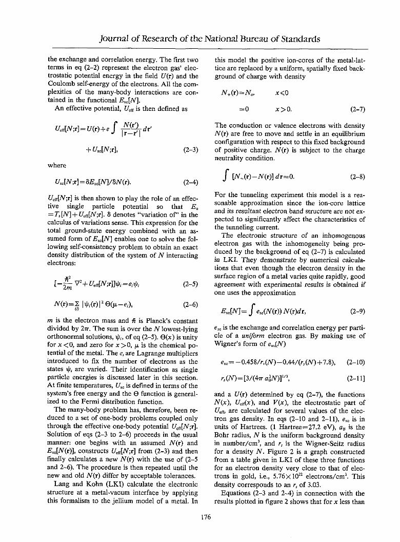
E. Clayton Teague An experiment has been completed rent versus spacing data. The analysiswhich demonstrated quantum mechani- suggests that van der Waals and electro-
National Bureau of Standards cal tunneling of electrons between two static forces play a major role in deter-Gaithersburg, MD 20899 gold electrodes separated in vacuum. mining the I-V characteristics and that
The tunneling current between the gold the tunneling area may be as small aselectrodes has been measured, for fixed 10-16 M2. Along with a review of thevoltages of 0.1 and 0.01 volts, as the theory of work functions and quantumelectrode spacing was varied from a dis- mechanical tunneling, numerical calcula-tance of approximately 2.0 nm down to tions of the tunneling current based ona point where the electrodes touched. the free-electron model of the electrodesCurrent changes of over five orders of and the barrier, an image-potential re-magnitude were found for electrode duced barrier, and a WKB approxima-spacing changes of approximately 1.2 tion for the tunneling probability havenm. For the first time, these data enable been performed and compared withone to deduce the work function of the Simmons' theory and with the experi-electrodes in a tunneling experiment mental results.from experimental parameters indepen-dent of the tunneling device. Also ob-tained were current-voltage charac- Key words: metal-vacuum-metal tunnel-teristics for fixed electrode spacings in ing; point-contact diode; scanning tun-the direct tunneling region where elec- neling microscopy; temperature control;trode spacings were less than 2.0 nm. tunneling theory; vacuum tunneling; vi-An analysis is given which attempts to bration isolation; work functiondeduce an absolute electrode spacingand tunneling area from the nonlinearproperties of the I-V data and the cur- Accepted: April 24, 1986
Preface
The following paper is a reproduction of the au-thor's dissertation which was completed and sub-mitted to North Texas State University in August1978. A majority of the experimental work wasperformed at the National Bureau of Standards.Results from the experiments were first reported atthe Spring 1978 APS meeting and later at a Na-
tional Science Foundation Workshop on Opportu-nities for Microstructures Science, Engineering,and Technology held in Airlie, VA, November 19-22, 1978. While a complete description of the ex-periments and results is available as a publicationfrom University Microfilms, publication in themore accessible form represented here has beenprompted by requests from colleagues and by thesignificant number of recent references to thework. In accordance with the requests, the Boardof Editors of the Journal of Research has agreed topublish the document unchanged except for the ad-
171
About the Author: E. Clayton Teague is with theCenter for Manufacturing Engineering in the NBSNational Engineering Laboratory.

Journal of Research of the National Bureau of Standards
ContentsPreface .......................... 171
1. Introduction.
2. Some Basic Concepts of Metal.Vacuum-Metal Tunneling Theory....
The Work Function and the ImagePotential ...........................
The Barrier Potential Energy Function ..The Tunneling Process .................Approximate Analytical Expressions forTunneling Current....................
Numerical Calculations of TunnelingCurrent .............................
Current Calculations for SphericalElectrodes ...........................
3. Experimental Apparatus andMethod.........................
Mechanical and Thermal Requirements ...Choosing an Electrode Material and
Preparing the Electrodes ..............Temperature Control System............Vacuum System for the TunnelingExperiment ..........................
Electrode Holder and MicropositioningAssembly ............................
Vibration and Acoustical Isolation .......Tunneling Electronics..................
4. Experimental Results and Analysis ..
Data and Analysis .....................Effects of Mechanical Stress on TunnelingCharacteristics .......................
Conclusions ...........................Acknowledgments .....................
172
174
175180183
186
188
195
195
195
196199
201
202205206
207
208
213215215
Appendices
1. NUMERICAL CALCULATIONS OFTUNNELING CURRENT.............
11. STATISTICAL FLUCTUATIONS INTHE LENGTH OF A BAR............
Ill. VACUUM CONDITIONS TOACHIEVE AND MAINTAINA CLEAN SOLID SURFACE .........
IV. AN ELECTRONIC DEVICE UTILIZ-ING QUANTUM MECHANICALTUNNELING ........................
V. ELECTRONICS FOR THE TEMPERA-TURE CONTROL SYSTEM...........
216
221
222
223
225
References ...... 232
dition of footnotes to identify recent work towhich it is closely related.
Renewed interest in these experiments has pri-marily resulted from the success and current wide-spread use of the scanning tunneling microscope(STM) introduced by Binning and Rohrer.' Thefindings of this work on vacuum tunneling shouldbe of interest to many who are using or planninguse of the STM. The current vs. voltage data, cur-rent vs. electrode spacing data, needs for tempera-ture stability, and observations about the potentialinfluences of van der Waals forces in these staticnon-servoed tunneling experiments are importantin understanding the servoed operation used fortunneling in the STM. While servoed operationovercomes much of the sensitivity of the STM toeffects from vibration, thermal expansions, and ma-terials instabilities in the electrodes, these effectsare proving to be significant factors in determiningthe stability and reproducibility of STM operation.
1. Introduction
According to quantum mechanics, a materialparticle can pass through a spatial region in whichthe particle's kinetic energy is less than its potentialenergy. The phenomenon is known as tunneling. Amacroscopic example would be a ball which, whenrolled toward a sharply peaked hill with insuffi-cient speed to get over the top, does not roll back,but appears on the other side of the hill withoutaffecting the ball or the hill and continues on itsway. The probability of such an event occurring isastronomically small at the macroscopic level.However, for electrons and other fundamental par-ticles and walls formed by nuclear and atomicforces, the probability while still small (one in 109 isnot unusual) leads to major physical effects [1]2.This work pertains to the tunneling of electronsbetween two metal plates closely spaced in vac-uum.
Tunneling is not a new idea; it is in fact almost asold as quantum mechanics. In less than two yearsafter Schrddinger [2] had published his now classicpapers on "Quantization as a Problem of ProperValues," Oppenheimer [3] had used the wave me-
'Binnig, G.; H. Rohrer, Ch. Gerber, and E. Wiebel, Surfacestudies by scanning tunneling microscopy, Phys. Rev. Lett. 49(1982) 57; and Binnig, G., and H. Rohrer, Scanning tunnelingmicroscopy, Helv. Phys. Acta 55 (1982) 726.
2Figures in brackets indicate literature references.
172

Journal of Research of the National Bureau of Standards
chanical concept of tunneling to explain the au-toionization of atomic hydrogen, Fowler andNordheim [4] had explained the main features ofelectron emission from cold metals in high externalfields, and Gamow [5] had described the alpha par-ticle decay process in heavy nuclei. The efforts byFrenkel [6] and by Holm [7] to describe the anoma-lous temperature dependence of the resistance ofelectrical contacts were the earliest studies of elec-tron tunneling between metals.
Since these early studies, electron tunneling insolids has remained a very active area of solid statephysics. Discoveries over the last 15 years by Gi-aever [8] that tunneling could be used to measurethe properties of superconductors, by Esaki [9] ofinterband tunneling in semi-conductors, by Joseph-son [10] of the unique characteristics of tunnelingbetween superconductors, and Lambe and Jakelvic[11] that tunneling could be used as a spectroscopictool have had a major influence on the develop-ment of physics, and all have important technologi-cal consequences.
In the simplest form, an experiment to measureelectron tunneling between two metals would beperformed as shown in figure 1(a). Two parallelplates are separated by an insulator and connectedto a variable voltage source. An ammeter and volt-meter are also included to measure the currentflow and the applied voltage. Normally, a directcurrent would not flow through the circuit. How-ever, if the plates are spaced very close together(on the order of 10 atomic diameters), a tunnelingcurrent will flow. If the plates could be made suffi-ciently flat and parallel over an area of one squaremillimeter, the current flow would be several am-peres for an applied voltage of one-tenth volt.
Conventional devices for conducting these ex-periments are fabricated by evaporating one elec-
trode onto a glass substrate, forming an oxide layerwith a fixed thickness of I to 3 nm on the electrodeand then evaporating a second electrode over theoxide layer. These experiments have been widelyused to measure the characteristics of Josephsonjunction devices, electrons and phonons in super-conductors, semiconductor surfaces and junctions,the material used for the insulating barrier, and in-tentionally introduced impurities at the barrier-electrode interface. While these experiments havemade and continue to make valuable contributionsto solid state physics and technology, they havebeen seriously restricted by the small number ofelectrode materials which tend to form natural ox-ides suitable for a tunneling barrier. In addition,interpretation of the experimental results has beenlimited because of the difficulties in characterizingthe atomic structure and composition of the insula-tor and the insulator-electrode interfaces. A majorproblem resulting from this lack of structure char-acterization is that the energy-momentum relation-ship of the electron while it is in the barrier cannotbe modeled adequately.
By making a change from these conventionaldevices to one which uses a vacuum barrier, mate-rial restrictions are removed, electron properties inthe barrier are well known, structure of the elec-trode-barrier interface is more defined and, in addi-tion, the electrode spacing may be continuouslychanged. There are, however, some difficultieswith vacuum barrier tunneling which must beweighed along with its advantages.
A schematic energy diagram for a metal-vac-uum-metal tunneling structure is shown in figure I(b). The energy diagram is based on Sommerfeld'selectron theory of metals in which all the conduc-tion electrons of a metal are considered as beingplaced in a potential energy box and distributed
MA
VARIABLEVOLTAGESOURCE
VACVM
WORK FUNCTIONFERMI ENERGY
LEVELS TUNNEL CURRENT
OCIE -.- -- APPLI ED VOLTAGEOCCUPIED ___
LEVEL _FERMISEA
Figure 1-Schematic of a Tunneling Experiment; (b) is fromGiaever [14].
173
(b)
PARALLEL

Journal of Research of the National Bureau of Standards
over the allowed energy values according toFermi-Dirac statistics. At zero temperature, theelectrons, therefore, fill the energy levels up to amaximum energy, the Fermi energy. The energyrequired to remove one of the electrons from thisenergy to a large distance from the metal is knownas the metal's work function. As shown in the fig-ure, when a voltage is applied to one of the metals,its Fermi energy is lowered relative to the other;the energy difference is equal to the product of themagnitude of the charge on an electron and theapplied voltage.
It will be shown in section 2 that an approximateexpression for the tunneling current, I, under theseconditions is given by
I = C exp(-aSB "2 )A V, (1-1)
where C33. 16X l10' A/m 2 /V, a = 10.25 (nm)-'(eV)" 1/
2, S is the electrode spacing, B is the average
barrier height for an electron at the Fermi energy,A is the tunneling area, and V is the appliedvoltage. The important consequences of eq (1-1)for the vacuum tunneling experiment are that smallchanges in electrode spacing or mean barrierheight have a very large effect on the tunnelingcurrent. A change in electrode spacing of 0.1 nmproduces approximately a factor of 10 change inthe tunneling current for a mean barrier height of 5eV. Changes of about half this magnitude can beproduced as a result of work function changes pro-duced by the formation of oxide or other films onthe electrode surface. Thus great care must be ex-ercised in electrode preparation and in the mechan-ical and thermal design of the vacuum tunnelingdevice.
Young et al. [12] and Thompson and Hanrahan[13] have previously performed vacuum barriertunneling experiments. Both of these experimentswere primarily concerned with observing the tran-sition from Fowler-Nordheim field emission tun-neling to direct vacuum tunneling. Young et al.[12] did report a preliminary observation of a linearcurrent-voltage characteristic for direct tunnelingat a spacing of approximately 1.2 nm. Thompsonand Hanrahan [13] have not reported any current-voltage characteristics. Uncontrolled fluctuationsin electrode spacing limited the exploration of di-rect vacuum tunneling properties in both experi-ments.
The objective of this work, which has evolvedfrom that of Young et al., was to extend the previ-ous vacuum barrier investigations to a detailed ex-perimental study of the direct vacuum tunnelingregion. Such detailed experimental results would
provide a means to test the present theoreticalframework of electron tunneling between solids.Some of the unresolved questions in this area: 1)What is the relationship between the classical elec-trostatic image potential and the quantum mechani-cal exchange and correlation potential? 2) What isthe transit time for a tunneling electron? and 3)How is the distance between the last atomic planesof the two electrodes related to the tunneling bar-rier thickness?
Explicit goals of this work, which were partiallyachieved, were first, to measure the currentthrough a vacuum tunneling device for fixedvoltages of less than one-tenth volt as the electrodespacing was varied from a distance of approxi-mately 2.0 nm down to a point where the elec-trodes touched; second, to measure thecurrent-voltage characteristics for fixed electrodespacing in the direct tunneling region; third, tocompare the measured results with available theo-ries of electron tunneling; and finally, to establish abasis for using a vacuum tunneling device for use asa probe to measure the position of a surface to aprecision of 0.1 nm, a precision 10 to 100 timesgreater than that of presently available techniques.Contributions to all these goals were obtained andwill be described in later sections. The qualificationon completely achieving the goals was given be-cause the quality of electrode surfaces and the pre-cision of electrode spacing measurements were notadequate in the area of the first three goals to re-solve completely the questions posed about the the-oretical framework.
A discussion of some fundamental concepts re-lated to electron tunneling in solids, with particularemphasis on the origin of the work function andthe barrier potential energy function, is given insection 2. Section 3 describes the requirements ofthe experimental apparatus for a vacuum tunnelingexperiment and the particular solution adopted forthis work. Experimental results and an analysis ofthe relationship between the results and the numer-ical calculations of section 2 are given in section 4.
2. Some Basic Concepts of Metal-Vacuum-Metal Tunneling Theory
The objective of this section is to calculate, withthe use of simple models, the current versusvoltage (I- V) characteristics and, for a fixedvoltage, the current versus spacing (Iv-S) charac-teristics of the gold-vacuum-gold tunneling deviceused in the experiments of this work. The primaryresults of these calculations are tables and graphs of
174

Journal of Research of the National Bureau of Standards
the I-V and Ic,-S characteristics which can beused for comparison with the measured data to bepresented in section 4.
While quite thorough treatments of electron tun-neling in conventional metal-insulator-metal junc-tions are available in the literature [14-23], nonumerical results have previously been publishedwhich fully accounted for the image potential vari-ation with electrode spacing and applied biasvoltage, both of which are essential for comparisonwith the metal-vacuum-metal tunneling data. Addi-tional motivations for performing the calculationswere that 1) almost all of the available theoreticalresults have been seriously questioned in terms ofnumerical accuracy and overall validity of the ana-lytical approximations which were employed [24],and 2) even if one were to accept the validity ofresults which have been obtained, the effort to ex-trapolate and apply these approximate results5 tothe gold-vacuum-gold tunneling device would bealmost as great as carrying out the more accuratenumerical calculations.
The content of the following discussion is there-fore 1) a description of models of the electronproperties of the tunneling device and of the tun-neling process, 2) a development based on thesemodels to obtain analytical expressions for the tun-neling current which are, within the limitations ofthe models, "almost" exact, 3) a reduction of theexact expressions with commonly used approxima-tions to obtain analytical solutions for I vs. V and Sin terms of experimental parameters, and 4) a de-scription of the procedure employed to carry outnumerical computations of I vs. V and S along witha presentation of results from these computations.No attempt will be made to give either a review ora comprehensive survey of the literature that is re-lated to the topics of this chapter. Tutorial cover-ages of the theoretical and experimental aspects ofelectron tunneling into semiconductors, metals,and superconductors are given in the book editedby E. Burstein and S. Lundqvist [14]. A compre-hensive review and digest of the tunneling litera-ture up through 1969 has been given by C. B. Duke[15]. Recent development in the theories of tunnel-ing are covered in two papers of debate betweenT. E. Feuchtwang and C. Caroli et al. [21] andreferences contained therein.
The Work Function and the Image Potential
By its nature, the metal-vacuum-metal tunnelingdevice can be completely represented by a modelwhich accounts for the electron properties of twometal-vacuum interfaces and their interaction. Ne-
glecting for the moment the interaction, the prob-lem is then to obtain a model that adequatelydescribes a uniform metal and its interface to vac-uum. In this section properties of the metal-vacuuminterface will be developed in terms of the generaltheory of metal surfaces formulated by Lang andKohn; LKI [25], LKII [26], LKIII [27]. Their the-ory will be used as a basis to describe the origins ofthe metal work function and to obtain a potentialenergy function for the metal-vacuum interface.
Lang and Kohn's work is based on the density-functional theory of inhomogenous electron gassystems formulated by Hohenberg, Kohn, andSham (HKS) [28]. The HKS formalism is a self-consistent-field method and as such its fundamentalidea is to replace the actual interactions; electro-static, exchange, and correlation, between the elec-trons and the ion-cores by an interaction betweenone electron and an averaged self-consistent poten-tial produced by the other electrons and the ion-cores. It therefore fully accounts for the effects ofelectron exchange and correlation and is in princi-ple capable of providing exact results. Since theconcepts of this formalism will be used so exten-sively in the following discussion of the work func-tion and the surface potential energy function, abrief summary of the HKS theory, based in part ona review by Hedin and Lundqvist [29], will now begiven.
The theory rests on two hypotheses. One statesthat the ground-state wavefunction of an interact-ing many-electron system, and thus all ground-stateproperties, are functionals of the electron densityN(r). The other states that the ground state energyfor a given external potential U(r) can be written as
EJN(r)]= f U(r)N(r)dr±F[N(r)], (2-1)
where F is a universal functional of N, independentof the external potential U, and that E. is a mini-mum for the correct density function N(r).
With these hypotheses as a basis, HKS [28] fur-ther show that the total electronic ground-state en-ergy of a many-electron system in an externalpotential U(r) can be written in the following form:
E. [N] =e f U(r)N(r)dr
+ (e/2) I (r)N(r) drdr'' r-r'J
+ T,[N] +Exe[N]. (2-2)
The functional T, [N] is the kinetic energy of a non-interacting electron system, and EJC[N] represents
175
Journal of Research of the National Bureau of Standards
the exchange and correlation energy. The first twoterms in eq (2-2) represent the electron gas' elec-trostatic potential energy in the field U(r) and theCoulomb self-energy of the electrons. All the com-plexities of the many-body interactions are con-tained in the functional ECEN].
An effective potential, Ueff is then defined as
Utff[N;r]=U(r)+ef l',? dr'
+ Uc[N;r], (2-3)
where
this model the positive ion-cores of the metal-lat-tice are replaced by a uniform, spatially fixed back-ground of charge with density
N+(r)=N_, xCO
x>O. (2-7)
The conduction or valence electrons with densityN(r) are free to move and settle in an equilibriumconfiguration with respect to this fixed backgroundof positive charge. N(r) is subject to the chargeneutrality condition.
U1c[N;r] = 8E,,[N]/8N(r). (2-4)
Ueff[N;r] is then shown to play the role of an effec-tive single particle potential so that E,=T,[N]+Urff[N;r]. 8 denotes "variation of" in thecalculus of variations sense. This expression for thetotal ground-state energy combined with an as-sumed form of E, 0 [N] enables one to solve the fol-lowing self-consistency problem to obtain an exactdensity distribution of the system of N interactingelectrons:
h2[-Si 7 2+Uegl[N;r]]4ii=e+,4 (2-5)
N(r)=2 I*,(r)12O(pj-e,), (2-6)(0)
m is the electron mass and { is Planck's constantdivided by 2ff. The sum is over the N lowest-lyingorthonormal solutions, +i, of eq (2-5). E<(x) is unityfor x <0, and zero for x >0, Zt is the chemical po-tential of the metal. The ei are Lagrange multipliersintroduced to fix the number of electrons as thestates +i; are varied. Their identification as singleparticle energies is discussed later in this section.At finite temperatures, U,. is defined in terms of thesystem's free energy and the e function is general-ized to the Fermi distribution function.
The many-body problem has, therefore, been re-duced to a set of one-body problems coupled onlythrough the effective one-body potential Ueff[N;r].Solution of eqs (2-3 to 2-6) proceeds in the usualmanner: one begins with an assumed N(r) andEJ[N(r)], constructs Uff[N;r] from (2-3) and thenfinally calculates a new N(r) with the use of (2-5and 2-6). The procedure is then repeated until thenew and old N(r) differ by acceptable tolerances.
Lang and Kohn (LKI) calculate the electronicstructure at a metal-vacum interface by applyingthis formalism to the jellium model of a metal. In
f [N+(r)-N(r)]dr=0 (2-8)
For the tunneling experiment this model is a rea-sonable approximation since the ion-core latticeand its resultant electron band structure are not ex-pected to significantly affect the characteristics ofthe tunneling current.
The electronic structure of an inhomogenouselectron gas with the inhomogeneity being pro-duced by the background of eq (2-7) is calculatedin LKI. They demonstrate by numerical calcula-tions that even though the electron density in thesurface region of a metal varies quite rapidly, goodagreement with experimental results is obtained ifone uses the approximation
EXC[NJ = f e.c(N(r)) N(r)dr, (2-9)
e., is the exchange and correlation energy per parti-cle of a uniform electron gas. By making use ofWigner's form of eSN)
e,, -0.458/r,(N)-0.44/(r,(N) + 7.8), (2-10)
r,(N)= [3/(4fr aV)] 1/3, (2-11]
and a U(r) determined by eq (2-7), the functionsN(x), Uff(x), and V(x), the electrostatic part ofU,,r, are calculated for several values of the elec-tron gas density. In eqs (2-10 and 2-11), ex, is inunits of Hartrees. (I Hartree=27.2 eV), a, is theBohr radius, N is the uniform background densityin number/cm 3 , and r, is the Wigner-Seitz radiusfor a density N. Figure 2 is a graph constructedfrom a table given in LKI of these three functionsfor an electron density very close to that of elec-trons in gold, i.e., 5.76X 10"2 electrons/cm 3 . Thisdensity corresponds to an r, of 3.03.
Equations (2-3 and 2-4) in connection with theresults plotted in figure 2 shows that for x less than
176

Journal of Research of the National Bureau of Standards
5.0
Figure 2-Graph of Electron Den-sity, Effective Electron Poten-tial Energy, and ElectrostaticComponent of Potential Energyat a Metal-Vacuum Interface.The positive background den-sity corresponds to a Wigner-Seitz radius of 3. The graph isbased on data from a table in N.D. Lang and W. Kohn, Phys.Rev. II (1970) 4555.
EN
RG
U
2.;
e0e
-2.5
-S. 0
-7.5_-0.8
about -1.0 nm, U,, approaches a constant valuewithin the bulk of the material as anticipated.Equation (2-5) then simplifies to the one particleSchrddinger equation
[_-2 V2+ VE(-o )+M,0 (N.)]eft,. (2-12)2m
VE(- cc) is the electrostatic potential energy of anelectron in the metal interior; ,.,x(N) is the ex-change and correlation part of the total chemicalpotential I(N) of an infinite uniform gas of densityN. From the definitions given earlier for E,,[N]and erc, and the definition of the chemical potential,
lu..(N)=d ((Ne,,(N))1dn (2-13)
or
=e.c(N)+Nd(ec(N))/dn. (2-14)
If the zero of energy is chosen such that
VE(_ wO) + lu.(N.) =O. (2-15)
then the equation describing the electron motion inthe electrodes at distance greater than I nm fromthe surface is
-2 V2 i, =e1 lq. (2-16)2m-
Therefore, for the case when N(r) is a constant, theelectrons in an interacting gas move as free parti-cles.
Interpretation of the eigenvalues of eq (2-5) asthe excitation energies of the elementary excita-
EC
I.e TR0N
0.a D
E
0.6 SITY
0.4 X
N
N0 . a
g.e
-0.6 -0.4 -0.2 0.0 0.2 0.4 0.6DISTANCE *NM'*
tions of the electron gas is not valid for a generalUeff[N;r] [29-31]. However, arguments are pre-sented by Moruzzi et al. [31] that demonstrate thatfor most bulk simple metals this interpretation is avery good approximation. Slater [30] gives somenumerical estimates of the energy errors involvedin using this approximation for self-consistent cal-culations in atoms. Hedin and Lundqvist [29] con-sider the problem from the Green functionstandpoint and one may conclude from a compari-son of eq (2-5) with their equation for the excita-tion energies of quasielectrons that for uniformpositive backgrounds the resulting energies andthose of (2-5) would be the same. However,nonuniformities in the electron gas such as thatgenerated by the pseudopotentials of the ion-coresand the discontinuity at a metal surface cause allthe usual differences between one-electron theoryand many-electron theory to become manifest, i.e.,self-energy corrections, relaxation times, and dif-ferent energy-momentum relationships.
The work from eqs (2-1 through 2-16) may ap-pear an overly complex way of obtaining this free-electron result. However, the reader shouldobserve that in addition to the free-electron behav-ior, this approach has also, by eqs (2-12 and 2-15),very naturally given a means to determine thebinding energy of the lowest energy state. The re-sults also clearly demonstrate that the binding en-ergy is due both to the electrostatic energyproduced by the existence of a surface and to theenergy resulting from exchange and correlation.Finally, the development through the calculateds Uff has produced a realistic potential energy func-tion at a metal surface.
177

Journal of Research of the National Bureau of Standards
The work function, WF, of a metal provides thenecessary reference for relating V(- oo) to the vac-uum energy level. It is defined as the minimum en-ergy required to separate an electron from themetal at zero temperature. Thus,
WF=(V,(+ )+EN-,)-En (2-17)
where VE(+ co) is the total electrostatic potentialenergy far from the metal surface and E,, is theground state energy of the metal with M electrons.Arbitrary zeros of energy for Vand E do not affectthe esult of eq (2-17). The chemical potential ja ofa system is defined as EN-EN]. thus eq (2-17) canalso be written as:
WF= Vg(+ to) -U. ~u(2-18)
Since the electrostatic potential in the interior of ametal with and without a surface differs byV(- co), ,1 for a metal with a surface is
A= VE(- co)+Ep+gl(N 0 ), (2-19)
Ep is the Fermi energy of a degenerate electron gasof density Nl. WF is therefore
WF=[VE(+ cc)- VE(- c)]
-EF-ji.zc(Na). (2-20)
In a more compact form,
WF=AVE-A, (2-21)
where AVE=zVE(+o)-VE(-oo) and
(2-22)
In this form the WF is seen to consist of two com-ponents, a surface part AYE, which is the rise inmean electrostatic potential energy across themetal surface and A, a bulk part which is the intrin-sic bulk chemical potential of the electrons relativeto the mean electrostatic potential energy in thebulk interior. A VE is due to the dipole layer createdby the spilling-out of the electrons as shown by thedistribution in figure 2. All many-body effects arecontained in the exchange and correlation contri-butions to Pf and in their effect on the barrier poten-tial AVE,
Combining eq (2-20) with the zero energy con-vention of eq (2-15) shows that the lowest energyeigenvalue of eq (2-16) is at an energy of) [AVe+ ,(NS)] less than V(+O0). Eigenstates ofeq (2-16) are then according to the Pauli exclusionprinciple occupied at zero temperature from thisenergy up to the maximum value EF. A diagram ofthe electron energy as a function of x position inthe region of a metal vacuum interface is given infigure 3.
The work function of gold was estimated inLKJI by again using eq (2-13) and Wigner's ex-pression for e,,(N) to obtain p.; AVE was calculated
r
WORltFU NCT ION
cc)
Figure 3-Energies pertaining to work function definition. Rela-tive energy scale was adjusted to give ratios of the quantitiesindicated which were that obtained by Lang and Kohn forgold.
178
uXC UEFF)
I
F

Journal of Research of the National Bureau of Standards
from the double-layer solution of Poisson's equa-tion
AVE=(e2 /) fx[N(x)-N+(x)]dx (2-23)
and the density distributions obtained from self-consistent solutions of eqs (2-5 and 2-6). In eq (2-23), e is the electron charge and e0 is the free spacedielectric constant. The results for gold were (all inunits of electron volts)
EF=5.57, -6-75, AVE
=2.32, WF=3.50. (2-24)
Experimental values of the work function are [32]5.0±0.2 eV for polycrystalline samples; the uncer-tainty accounts for the range of values obtained byvarious experimental techniques. Attempts toachieve better agreement by incorporating latticeeffects through a pseudopotential were not success-ful.
It is not clear how the discrepancy between thetheoretical and experimental work functionsshould be apportioned between g4c and AVE. Butregardless of this difficulty, Lang and Kohn's cal-culations have shown in a definite way the relativemagnitudes of the two major contributing terms tothe work function. In addition, this insight intohow the work function energy is generated willlater prove useful in interpreting the effects of ab-sorbed molecular species on the values of the workfunction.
There remains one further significant questionabout the electron structure at a metal-vacuum in-terface: For purposes of a tunneling experiment,what is the potential energy of an electron I to 10nm outside a metal surface? A related questionwhich must also be answered is: Where is the effec-tive metal surface? Both questions are addressed inLKIII. By solving eqs (2-5 and 2-6) self-consis-tently, an N(r) is calculated from a Uheff determinedby the sum of the energies due to the distribution ofeq (2-7), a point charge outside the metal surface,and a weak external electric field F. The unper-turbed charge distribution produced by the chargedensity of eq (2-7) is then subtracted from this re-sult to obtain a screening charge density of N,(x).The potential energy of an electron outside the sur-face in the presence of a weak uniform electricfield pointing out of the metal is then calculated asthe interaction energy between the potential of thepoint charge, q, and its induced screening charge.
The result for a charge located at the position x, isto order (x,-x 0) 3' given by
VIp(x) = const-q 2 /[4ve0 (xj -x 0 )]
-qE(x -x). (2-25)
The center of mass, x0, of the induced screeningcharge is defined by
X0= fx N5 (x)dx /fN,(x)dx. (2-26)
For small fields, the center of mass of the inducedscreening charge is approximately the same as thatfor the point charge. The answer to the first ques-tion posed is, therefore, that the potential to a goodapproximation is the classical image potential re-ferred to a plane passing through x0 . Relative to theedge XB of the uniform positive-charge back-ground, the position x0 is determined byxo-xB=0.07 6 nm for an r,=3, i.e., gold's electrondensity. This value was obtained by interpolatingbetween the values of x0-X9 given in LKIII forr, = 2 and r, = 4. x0 and xB are located schematicallyin figure 4.
In connection with the problem of determiningthe potential at a metal surface, field penetrationeffects are often considered to be a significant fac-tor. As pointed out by Lang and Kohn, the analogyhere of penetration effects is just the fact that theinduced charge distributions have finite widths.
A definite answer for the second question is notas easily obtained. Locating XE of the positive back-ground model relative to the lattice of the metal isthe problem. The approach taken in LKIII was tolocate, somewhat arbitrarily, x1 at a point one-halfan interplanar spacing in front of the last plane ofions. A justification for this assignment can be ob-tained from the self-consistent calculations by Ap-plebaum and Hamann [34] for the Na (100) surfacein which the lattice properties and atomic nature ofthe surface were treated at the same level of detailas is common in bulk calculations. They give a fig-ure which shows the effective potential and chargedensity in much the same manner as figure 2, withthe ion-core locations shown. Taking the point atwhich the electron charge density has dropped toone-half the bulk value as the proper place to lo-cate the positive-background edge gives the x,value assumed by LKIII.
In summary, the electron potential outside a goldsurface is given by eq (2-25) with x0 located at apoint one-half an interplanar spacing plus 0.076 nmin front of the last plane of ions (see fig. 4). Thisalong with Ut ff is sufficient information to deter-
179

Journal of Research of the National Bureau of Standards
C IECRE I I I
,91g~e, I EffectiveI 1
Figue t Of ef v mMetal Surfaces 1 iu
>-L $2 VI. e e /2 ci o.o769l -p
ELECTRODE T ELECTRODE IT
Figure 4-Llocation of effective metal surfaces. Diagram illus-trates simple model of two identical gold electrodes with theatoms spaced at the nearest-neighbor distance in a gold crys-tal. The electrode spacing shown would correspond to a sepa-ration of the respective last ion planes of approximately 1.73nm; the nearest-neighbor distance was assumed to be 0.288nm.
mine the potential between two gold electrodes invacuum.
However, the effective spacing between theelectrodes for tunneling is reduced even more thantwice the sum just given since the tunneling dis-tance will, as shown later, be determined primarilyby the distance between the points of the elec-trodes at which Ueff=Ep. For gold (see fig. 2) theeffective tunneling surface, by this convention,would be located 0.105 nm plus one-half an inter-planar spacing in front of the last plane of ions.This is the distance obtained from figure 2 at whichUe,,=O; x, in figure 2 is at the ordinate 0. For aninterplanar spacing, d, the location of the gold sur-face for tunneling, x5, relative to the location of thelast plane of ions, xi, is therefore
x,=x,+0.5d+0.076 nm+t, (2-28)
where t is the distance from xO to where Ueff=EF;thus, t=0.105-0.076=0.029 nm. The positive xdirection is out of the metal surface.
At large, positive x, UJ,[N(r)] is thought to be-come the classical image potential [U1 c(x)-(e 2 /4ir eox)] [25,33]. However, no form of theexchange and correlation potential has as yet beenput forth which has the expected asymptotic func-tional dependence on x. The transition of an elec-tron from inside a metal in the presence of manyother electrons where energy changes result fromelectrons of like spin avoiding each other (ex-change) and electrons of either spin avoiding eachother to minimize the coulomb energy (correlation)to a region in vacuum where at least the correla-tion is an insignificant factor has been extremelydifficult to model. The slowly varying density ap-proximation for exc[N] given in eq (2-9) leads to aneffective exchange and correlation potential whichvanishes exponentially as x goes to infinity (seeLKI). A control calculation was performed in LKIby checking the self-consistent results against thatobtained when the image potential (1/x) form wasused for x values greater than the point whereUetf=EF. Differences in N(x) obtained with thetwo potentials were no greater than 0.3% forr,=2.5. The more commonly used Slater X-a ap-proximation for the exchange and correlation po-tential varies as N(x)1 1 3. With reasonable N(x)'s italso vanishes much more rapidly than l/x as x goesto infinity [34].
The Barrier Potential Energy Function
In this section and the following section on thetunneling process, the tunneling device is assumedto be composed of two semi-infinite metal elec-trodes with plane parallel faces separated by a vac-uum space. The parallel faces are taken to benormal to the x axis with electrode II located fur-ther along the positive x direction than electrode 1.
Assume first that the electrodes are in equi-librium with each other. Then, the chemical poten-tials of the two electrodes will be equal [35] and eq(2-19) gives
VE'(- co)+EF+pc(N)= VF'(- c)+EF
(2-29)
(2-27)The superscripts denote the electrode labels. Whenthe electrodes are not contacting this conditionor,
180
+ttl(ND).X� �Xi +(XB -Xi)+(XO-XB)+t

Journal of Research of the National Bureau of Standards
combined with the definition of the work functionin eq (2-20) requires that
VV=VE(+ )-VP(±Cc>WF'-WF 1 . (2-30)
Thus, if the two electrodes have different workfunctions, the equilibrium condition is for there toexist an electrostatic potential difference betweentheir surfaces. This potential difference is usuallyknown as the Volta or contact potential [36]. Re-cent work by Bennett and Duke 137] has, however,shown that the name contact potential would beinappropriate since they conclude that when themetals are in contact, the junction potential, V, is
V, = EF' + c(Nl) )- [E + 11 ac(Nal )] (2-31)
This result interpreted in terms of eq (2-29) meansthat when the electrodes are in contact, their back-ground electrostatic potentials, V(- c), are con-strained to be equal; a very reasonable conclusion.Bennett and Duke's [37] arguments are not basedon eq (2-29). Their results follow from solutions toSchrddinger's and Poisson's equations with appro-priate boundary conditions.
The problem of describing the transition be-tween the conditions specified by eqs (2-30 and 2-31) has, unfortunately for use in a general vacuumtunneling configuration, not been investigated. Forthe particular configuration, i.e., with almost iden-tical gold electrodes, used in the experiments ofthis work the effects from both V, and Vv wereminimal. In the following discussion, V' and V, areassumed to be zero for the gold-vacuum-gold tun-neling experiment.
Assuming equal Fermi energies and work func-tions in the two electrodes, the barrier potentialenergy function, VB(X) at equilibrium is, followingthe conventions of figure 3 given by
VB(x)=EF+ WF+ Vjp(x), (2-32)
where Vp(x) is the image potential of a pointcharge between two conductors with plane parallelfaces. The energy zero is assumed to be such thatVE(- o)+!4Q(n4)=O. The classical image poten-tial (2-25) is employed because of the difficultiesgiven earlier about the incorrect extrapolations ofavailable forms of the exchange and correlation po-tentials. In vacuum, the classical double image po-tential energy function is [38]
VIPW = ( -- 2 2ns ) (2-33)cITE 2x, =lw fl _XIflS
where s is the distance between the faces of the twoconductors and x is the coordinate relative to anorigin at the face of electrode L. To facilitate nu-merical calculations, a simpler approximate form ofeq (2-33) obtained by Simmons [38] will be used.The approximate form is
V,p(x)=-1. 15(1n2)e' 8
With s and x expressed in nm andvolts (eV), eq (2-34) reduces to
(2-34)
Vap(x) in electron
Vlp(x)= -0.2867 x(s-x) (2-35)
Plots of Vi(x) with the V4, of eq (2-35) and as-sumed electrode Fermi energies of 5.5 eV andwork functions of 5.0 eV for s values ranging from0.2 nm to 5.0 nm are given in figures 5 and 6. Notethat in these figures, the vacuum level is at an en-ergy of 10.5 eV. These graphs demonstrate that asthe electrode spacing decreases, the maximum bar-rier height drops by more than one electron voltwhen s = 1.0 nm; when s = 0.23 nm, the maximumbarrier height has dropped to the Fermi energy of5.5 eV. This is coincidentally about equal to thenearest-neighbor distance for the gold lattice.
For the barrier potential energy function plottedin figures 5 and 6 to correspond with the surfacelocation described by eq (2-28) and the correctionsto the classical image potential given in eq (2-25),the x =0 and x =s positions would correspond tothe x0 described in these equations. While t, thedistance from x0 to the x value at which Uff=EF,was found in LKIII to be 0.029 nm for gold, thevalue obtained from figure 5 is approximately 0.06nm. Neglecting for the moment the possible effectsof nonzero t, the modifications of eqs (2-25 and2-28) mean that tunneling currents calculated fromthe barrier potential with a spacing parameter sshould correspond to a true physical spacing, ST,
ST=Xj!a-xj' =S +d +0.152 nm. (2-36)
The importance of eq (2-36) will be discussed insection 4 when an attempt is made to relate thecalculated current values to measurements.
When the positive terminal of a battery of poten-tial Vis connected to electrode II and the negativeterminal to electrode 1, the mean electrostatic po-tential, for negative charges, of electrode 11 is low-ered by an energy of eV relative to that inelectrode I. Since the EF and x,,c are fixed by the
181

Journal of Research of the National Bureau of Standards
Figure 5-Barrier potential energyvs. distance for electrode spac-ings of 0.2 nm to 1.0 nam.
.Oo 0.1 5 0.20 0.25 0.30 0.345 0.50 0.35 0.60 65 0.70 0.75 0.80 0.80 o.05 1.00
DISTANCE FROM LEFT ELECTRODE IN NM
Figure 6-Barrier potential energyvs. distance for electrode spac-ings of 1.0 nm to 5.0 nm.
0.00 0.25 0.50 0.75 2.00 1.25 1.50 1.75 2.00 2.25 2.50 2.75 3.00 3.25 3.50 3.75 4.00 4.25 4.50 4.75 5.00
DISTANCE FROM LEFT ELECTRODE IN NM
electron density, the Fermi level is also lowered byan energy eV. Combining the barrier potential en-ergy function with this effect and assuming thefield between the electrodes is uniform gives a po-tential energy function for the metal-vacuum-metalsystem which can be subdivided into three areas ofinterest:
Region 1: VT(x)=O
Region 1i: Vr(x)=-eV x >;jix
Region III: VB(x)=E,>+ WF-eVx/s
+ Vyp(x)x'>x >x", (2-37)
182
C
1o
0'~
.1I
81j
C
9
.,
0o
0
g0
Cl
Q)
z1H-
H7
z04
-0.
c
UE.
I
E-.
4F-I-
H
Zx
CA
I
C-i
) oI
'
0 C
XoI
z sI
.9
Cl
-0.257

Journal of Research of the National Bureau of Standards
x' and x" are the values for which VB(x) is equal to0 and -eV, respectively. Figure 7 is a schematicillustration of eq (2-37) combined with the con-cepts of figure 3 concerning the work function.The areas of the diagram up to the Fermi energyrepresent eigenstates that are occupied when theelectrodes are at zero temperature.
The Tunneling Process
From this point onward in the theoretical devel-opment no further attempt will be made to accountfor many-electron effects on the calculated tunnel-ing current. All the previous work to account formany-electron effects was required since, asshown, the dominant sources of the work functionoriginate from electron-electron interactions andtheir effects on the electron distribution at a metalsurface. A fully independent-electron model-of theelectrodes and of the tunneling process will be usedin the remainder of this section. There were twomajor reasons for this decision. First, at the resolu-tions of I-V measurements anticipated for this ex-periment, the small changes in current due toelectron-electron interactions, electron-phonon in-teractions, and self-energy changes produced bytransition through the barrier would not be observ-able. The changes are usually less than one percent.Second, within the limitations of the independentelectron model, the stationary state method of cur-rent-carrying states is a well-defined and conve-nient procedure for calculating current flow inquantum systems [39,40].
For an electron described by one of the solu-tions, 4fk(r), to the time-independent Schrbdingerequation for the potential Vr(x)
[- ' + V-(x)] 4ik(r)=E(k)Ik(r), (2-38)
the electron current density flow is given by [40]
J(k,r)= 2m (4'k V4-4Vq k) (2-39)
where * denotes the complex conjugate operation.The standard interpretation of eq (2-39) is that J-nis the probability per unit time that a charge -ewill flow through the unit area with normal n.Since the electrons occupying the states Vk(r) areassumed to not interfere with each other, the totalcurrent density is just the sum of the current den-sity contributions from each eigenstate of themetal-vacuum-metal system which is allowed bythe Pauli exclusion principle.
The non-equilibrium aspects of a biased junctionare usually treated by assigning different thermaloccupational probability functions to each metalwith the reference energies offset by the appliedvoltage and differences in Fermi energies. Thus,with V'(-co)+p±j as the reference energy zeroand a positive polarity voltage, V, connected toelectrode II, the energies in the two electrodeswould be related by the energy conservation equa-tion:
E1 =EII+EFI-EF,,-eV. (2-40)
For a net current to flow, occupied states on oneside of the barrier must exist at the same energy asempty states on the other. In figure 7, the appliedvoltage will establish, at zero temperature, emptystates in electrode 11 opposite filled states with thesame energy in electrode I. Therefore, in this in-stance, electrons would dominantly flow fromelectrode I to electrode 11 by tunneling through thebarrier, i.e., via a current-carrying stationary statewhich existed in all three regions of the system.The current density is computed as the differencebetween the current density flowing from I to IIand II to 1.
The thermal occupational probabilities are givenby the Fermi-Dirac distribution
VACUUM LEVELy
z
I LFERMI ENERGY
AU ELECTRODEE:I
Figure 7-Energy Diagram forMetal-Vacuum-Metal Tunnel-ing. Energy and distance in thediagram are drawn to scale forthe quantities represented. Thesmall oscillations of the energyat the bottom of the occupiedstates represent the magnitudeand spacing of the ion-core po-tentials. X, and X, are the classi-cal turning points for anelectron near the Fermi energy.
183
7
VACUUMIVV Vv
Au ELECTRODE I
IWORK FUNCTI
00
XI
FERMI t I

Journal of Research of the National Bureau of Standards
f(E)=(1+eXp[E j D) (2-41)
where E is the energy eigenvalue, kg is Boltz-mann's constant and T is the system temperature.Equation (2-40) combined with eq (2-41) gives theresult
fl(E)=f(E)
f11(E) =f(E +eV). (2-42)
Again, taking the plane of the electrodes to be nor-mal to the x-direction, the current density, J1r-,:from I to 11 is then given by
(2-43)JI- = 27 J1_j(kr)f,(E)[ l-f,(E)] .
electrode faces, and A is the area of the tunnelingdevice; Mk,(x) is defined below. The eigenvaluesE(k) are
E(k)= (k + kA) = 2- (2-47)
Let x,(E) and xR(E) be the classical turning pointsfor the energy E at electrode I and electrode II,respectively, then with Merzbacher's conventions
Mk,(x)=A k-' 2(x)W+
+Bk--'(x) W
M, (x) = CK - "2(x) Z
+DK- 112(x) Z+
X .•XL(E)
XL<X <X,
The factor of 2 is to account for the additionalstates produced by the two electron spin orienta-tions. J'r-H is the x component of J(k,r). Similarly,
(2-44)
Since VT(x) is a real potential, the solutions toSchrddinger's equation must obey the general re-ciprocity theorem of scattering processes. Blatt andWeisskopf [41] give a succinct statement of the the-orem: "This theorem states that the probability fora transition proceeding one way in time is equal tothe probability for the same transition, but with thesense of time reversed," The sense of time in eqs(2-43 and 2-44) is manifest only in the direction ofthe wave vector, thus, Ji(kr)=Jt- 1 1 (-kr)=Jt,_i(kr). The expression for the net current den-sity is therefore
MkX(x) =F k -'2(x) q+
+Gk-'`(x)q_where
W+=exp[+ if k.(x)dx]
Z+ =exp v-f KX (x)dx]
q± =exp [4- i kx(x)dx]
and
XR(E)}x, (2-48)
(2-49)
K(x)= r2 V.x)-(E(k) 2l)11/2,Lhll2\ k 2m1JJ (2-50)
With these conventions, Bohm 143] then shows indetail that with the use of connection formulas
J== 22 J'(k,r) [[f() -f(E + eV)J. (2-45) A =!(l/2)(2e+ 1/(2e)]F
To calculate J 5(k,r)=JX(k,r) (a subscript nota-tion is adopted hereafter), explicit solutions to eq(2-38) for all three regions of Vr(x) must be ob-tained. The solutions given here will be based onthe results obtained by Merzbacher [42] with theuse of the Wentzel, Kramers, Brillouin (WKB) ap-proximation technique for solving Schrodinger'sequation. If periodic boundary conditions are im-posed in the y and z directions, the solutions to eq(2-38) may be written as
(2-46)
where k. and P are the wave vector and displace-ment, respectively, parallel to the electrode faces,k, is the wave vector component normal to the
where
e=exp ( X K(x)dx). (2-52)
If now the solution in region I is assumed to be
M"., W e'-l+R e`-'k (2-53)
with R being adjusted for normalization, then thesolution in region II is, assuming G=0, i.e., nowave is incident from right,
MIk (x)=2[2ej+- /(2e)L' eks(5Lx-R) e'kx. (2-54)
The conservation of kJ and total energy in the tun-neling process was implicitly assumed in the calcu-
184
(2-51)
J11_i=2Y_ J11_1(kr)f11(E)[l -fl(E)].
Y1 k(r)=14 " exp(ik,-P)Mk,(x),

Journal of Research of the National Bureau of Standards
lations from eqs (2-46 to 2-54). Since MkP (x) is thestationary state solution in region 11 and probabilitycurrent is "conserved," it may be used as well asthe solution in the other two regions to calculatethe current density. Substituting eq (2-54) into eq(2-46) and then the result into eq (2-39) gives
J~k,r)=4[20+l1/(20)] _2 ehk /m . (2-55)
Let
D(E, k,) = 4[0 + 1//(0)]2, (2-56)
then
J.(k,r)=D(E, k,) eik./m. (2-57)
D(E,k,) may be interpreted as a transmission coef-ficient for the part of the solution in region I intoregion I1.
Substituting eq (2-57) into eq (2-45) gives thecomplete expression for the current density J as
J=2eAf/m ! k D(E, k,) [(E)k
-f(E+eV)]. (2-58)
The summations are most conveniently carried outby changing to integrations over the variable E.defined as
E. =A'k./2m =E(k) -A'/2m. (2-59)
The conversion is performed with the followingthree relations: the first is the well known sum tointegral conversion in k-space, the second one isbased on the free-electron properties expressed ineq (2-47) and the third is the differential of eq(2-59):
d )k =3k/(27r)3
d 2k, = (27r m IA')dE,
kxdkx =(m /Ah2)dEx . (2-60)
With these relationships, eq (2-58) may be writtenin the following form:
J = f dEZ D(E) N(E,,)
N(Ex)=(4frme/h3 ) fJ [f(E)
-f(E + eV)]de, .
In words this states that the net current density isequal to the sum of the number of electrons withthe "x-part of their energy" within dE, that areincident on the surface of the negatively biasedelectrode per unit time per unit area, N(E,)dE.,times the tunneling probability of an electron atthis energy, D(EJ)
This is the same form of the equations obtainedby Duke [44] and as such is an acknowledgmentthat his work was frequently consulted in develop-ing eqs (2-61). Another form of eq (2-61a) which ismore useful for interpreting the energy aspects ofthe tunneling process is
J=2*e fdE f(E) -f(E +eV)]
f 2ir-d2kpD(E,kp). (2-61c)
Equation (2-61c) facilitates the physical interpreta-tion of the origins of the tunneling current in termsof the overlapping of energy surface projectionsonto the tunneling plane and enables direct connec-tion with energy diagrams such as that given infigure 7. However, calculation of the tunnelingcurrent, particularly for the free-electron model ofthe electrodes, is most easily accomplished withthe use of eq (2-61a).
Equation (2-61b) may be integrated by parts toobtain
N(E,)=(4 mekBT/h3 ) in (FDI/FDII),
FDI= I+exp [(EF-EB)/kBTI
FDII= 1 +exp [EF-E. -eV)/kBT]. (2-61d)
Note that the Fermi energies of the two electrodeshave been assumed equal. Collecting all the defini-tions involved in eq (2-56) together for referencegives
D (Ex) =4[20 + 1/(20)]2,
e =exp (fr K(x)dx),
K(x)= [2m /'ii)(VB(X)-EX)1 11 2,
VB(x)=EF+WF-eVx/s
-(const)s[x(s -x)]-',
const = 1.1 5(1n2)e '/81reo(2-61a)
=0.2867(eV nm). (2-61e)
The accuracy of the WKB approximation for(2-61b) calculating the transmission coefficient has been
185

Journal of Research of the National Bureau of Standards
extensively investigated in the literature of thisfield. One of the most thorough checks was per-formed by Politzer [45), who compared valuescomputed with the form
rAR
D(E)=exp[-2fJ K(x)dx], (2-62)
of the WKB transmission coefficient with those ob-tained from a numerical solution of Schrbdinger'sequation using essentially the same Vr as given ineq (2-37). Her results show that the WKB result isvalid at the fields and energies involved in mostconfigurations of the vacuum tunneling experi-ment, i.e., fields less than 102 V/cm and energiesmuch less than barrier height.
The major difference between the exact resultsand the WKB approximation was that the exactD(E) was an oscillatory function of energy for en-ergies and fields which resulted in an effectivebound state potential well above the top of the bar-rier. The amplitude of the oscillations in the exactD(E) was relatively small and such that
0.5 <Log(D(E)wK0/D(E)NUM) <0.8
N(E,)=ATeV, Of E0 EF-eV
=0
A, is the "thermal" constant 4ir me/h'. Thus, eq(2-61a) takes the form
A eF CV
J=A2[CeVfrEF
+EP,-eV (EF-E)D(E1JdEJ, (2-65)
For large e in eq (2-61e), which for most barriersin tunneling experiments is a true condition, D(E,)can be approximated by the form given in eq (2-62). Simmons [46] has proposed an average barrierheight method to further simplify D(E,). His ap-proach is to approximate the integral in eq (2-61e)over K(x) with an average barrier height, B, abovethe Fermi level of the negatively biased electrode,i.e., he defines B as
B = W-T ALVY(x)dx,(2-63)
for all fields and for energies more than 0.5 eVfrom the top of the potential barrier. Near theFermi energy, at which the major contribution tothe tunneling current occurs, the ratio's mean valuewas about -0.2. The mean difference between thetunneling current for the two calculations of D(E)was not calculated by Politzer, and barrier heightsapplicable to the vacuum tunneling experimentwere not investigated.
Approximate Analytical Expressions for TunnelingCurrent
In this section, the qualitative properties of thetunneling current will be derived from the zerotemperature, low voltage solutions to eqs (2-61 a toe). The overall character of the tunneling currentwill be shown to be approximately ohmic with asmall cubic dependence on voltage having impor-tance at higher voltages. At all voltages, the tun-neling current is found to be exponentiallydependent on the electrode spacing. Finally, thezero temperature solutions are extended to finitetemperatures and estimates of the effects of roomtemperature on the tunneling current are given.
The tunneling characteristics determined by eqs(2-61) are most easily understood by first investi-gating the zero temperature behavior. At zero tem-perature
where XLF and x,, are the classical turning pointsfor E,=E,, and W~=Xp-XLF is the width of thebarrier at this energy.
With this definition, Simmons [46] shows that forvoltages of less than about one volt
D(E,)=exp[-aW(EF+B -E)`1],
a=(47r/h)(2m)"1 =l0.24(eV)-'2 nm-'. By utiliz-ing this D(E.), an approximate low voltage tunnel-ing current density can be calculated from eq(2-65). Let N=E4-.E amdp =aWB ", then eq (2-65) may be written as
J=Ar{-eVf exp[-p(1l+n/B)'fdN
- N exp[-p(l +N/B)'i]}dN. (2-68)
For small voltage, A/B, will be much less thanone, so the approximation (l+N/B)' 2 =(l+N1/2B) may be used. The integrals may then be evalu-ated to obtain the result:
J =A r[(4e -P/(a W)2)
(2-69)
Only a factor of exp(- a WEF/Blf2) was neglectedto obtain eq (2-68). If one takes just the leadingterm in the series for the exponential, the following
186
EF-eV<E <EF
(2-64)
D (E)d.E,
(2-66)
(2-67)
EF~,E,
x (I -exp[-aWeV/(2B`)])J.

Journal of Research of the National Bureau of Standards
result for the tunneling current density at low biasvoltages and zero temperature is obtained:
JL(T= 0)=JOL exp(-p)V, (2-70)
where JOL=[(2m)"./.lWf(e/h) 2 B1 . If B is ex-pressed in eV and W in nm, JOL is
J,= 3.16 X 10' B"5 W' (A/m2 /V). (2-71)
By evaluating eq (2-68) in a more exact manner,Simmons [46] derives a general formula for the cur-rent density at zero temperature. The formula andits associated relations are given below in what hasbeen found to be a consistent algebraic form, whichdue to misprints, etc., is not correct in publishedforms. It is given here because it will be used forcomparing with the numerical results of the nextsection. With the same definitions given in eqs (2-66 and 2-67), the formula is
J(T=O)=J4(B exp(-aWB'"2)
-(.8 +eV)exp[-aW(B+eV)"21),
J0 =e(2Trh)-' W-2
=6.2X 10¹²W-2(A nmnl/(m2- eV). (2-72a)
Based on eq (2-66), the analytic approximation forB including image potential effect is
B = WF-(V/25)(S +S2 )-[0.286/(s2-S1)]
Xln[S2( -S)/(S(S -S2 ))] (2-72b)
S = electrode spacing in same sense as previouslydiscussed.
S,=0.31WF
S2 =S[I -2.3/(3 WFS + 10- 2VS)1+S¶.
In eq (2-72b), the work function should be ex-pressed in electron volts and all distances involvedin nanometers.
Equation (2-72a) reduces quite easily to eq (2-70) by expanding both exponentials in a series andneglecting terms containing V2 and higher orders.However, if one keeps all terms out through V3, itis found that the quadratic terms cancel to give thenext higher order approximate result [19]. Foridentical electrodes
J(T=°)=JOL[V+U3S2/B)V3], (2-73a)
with
j3=(7r2me/h2)=3 27 V' nm-. (2-73b)
This value of j, was taken from the results ofBrinkman et al. [19] who expanded eqs (2-61) inpowers of the voltage and obtained approximateexpressions for the coefficients of the linear andquadratic terms of the conductance. They consid-ered eq (2-73b) to be accurate to within 10% fortrapezoidal shaped barriers and where S is greaterthan I nm. An earlier value obtained by Simmons[47] for the same conditions wasj 3= 1.15 V-' nm- 2 .No calculations ofj 3 with image potentials correc-tions are available in the literature. In spite of therelatively unknown values for this constant, thequalitative behavior predicted by eq (2-73a) hasbeen fairly well established in many different ex-periments [48,49,19r.
In summary, the ideal tunneling characteristicsare then as follows:
I) Current density varies exponentially withelectrode spacing, with an exponent of -10.25 Xmean barrier height in electron volts X electrodespacing in nanometers.
2) The current-voltage characteristic should besymmetric for identical electrodes. (This justserves as a check on the formalism or the experi-mental method since it must be true if the elec-trodes are truly identical.)
3) For low voltages, the current-voltage charac-teristic is approximately ohmic.
4) For voltages up to the work function, the non-ohmic conduction should be dominantly a cubicfunction of the applied voltage, with higher orderterms becoming more important as the voltage isincreased up to the work function.
The extension of the previous results to finitetemperatures is the last topic to be discussed in thissection. If the approximations which led to eq (2-68) are substituted into eqs (2-61), the followingresult is obtained:
J(T)=AJkATexp(-aWB" 2)
X f In(FDI/FDz)
exp(-a WN/2B1'2)dN, (2-74)
where again N=EF-E,. When k,1 T is less than2B" 2 /aW, the integral may be evaluated by thetechniques of Murphy and Good [50] to obtain
187

Journal of Research of the National Bureau of Standards
a J(f)=A Q-4[QkBT/sin(wrQkBT)]Xexp
(-p)[l-exp(-QeV)], (2-75)
where Q=(1/2)aWB" 2 . For Tapproaching zero,the factor in the first bracket goes to one, and Sim-mons [46] shows that the remainder of the termsare equal to J(T=0). Therefore,
J(T)/J(T = 0) = QkBT/sin(7rQkaT). (2-76)
Q is typically less than 4(eV)-'. The argument ofthe sine is therefore much less than one at roomtemperature. The series expansion gives
J(T)/J(T = 0)= I+(l/6)(irQkET)2
or in practical units (2-77)
J(T) =J(T=0)(1 + [3 X 10- "(eV/mn2 /K2)
(WT)2/B]).
For W=I nm, T=300 K, and B=2 eV;J(T)= 1.013 J(T=0). Such small changes in thetunneling current would not be detectable with thepresent experiment. No significant effect from con-ducting the experiment at room temperature wastherefore anticipated.
PROD US. ENERGY T-300. EFS .5X4014
PR0D
A
/!C
3
a
I
'8
2 3 4 5
ENERGY teV*
Numerical Calculations of Tunneling Current
In order to facilitate the analysis of measured I-Vand I,,-S tunneling data, the following calcula-tions, based on eqs (2-61) were performed. The re-sults are given in accompanying figures and tables.
1) The product of D(E.)N(E.) as a function ofEX for four voltages; 0.001, 0.010, 0.10, and 1.0 V,at each of three electrode spacings; S =0.3, 1.0, and2.0 mu. See figures 8, 9, and 10.
2) For a simple model of the tunneling betweenspherical electrodes, described below, calculationsof the tunneling current density and current weremade for a fixed bias voltage of 0.1 V as a functionof electrode spacing and work function. Computa-tion times were long for the current calculations,15 seconds per data point, so only a limited numberwere obtained. These results are given in table Iand figures 11 through 17. The graphs in figures 11and 12 were at first plotted in a normalized form,but after finding that much information was lostbecause of the large orders of magnitude changesbetween graphs, the four separate graphs werechosen as the more useful representation. Figure 11shows the changes in curvature or lack thereof inthe I- V for a spacing of 2000 pm. Figure 12 showsthe increase in curvature of the l-V characteristicas a function of electrode spacing for a fixed workfunction of 4.5 eV. Figures 13-17 are graphs of thedata in table 1 and enable a comparison of the cur-
LSFP5.0 D-0.3
Figure 8-Distribution of energyassociated with normal compo-nent of tunneling electron mo-mentum; electrode spacing of0.3 arm The Fermi energy, F,and the work function, WF, are
6 in units of electron volts.
188

Journal of Research of the National Bureau of Standards
X107 PROD US. ENERGY T-300. ES.5 FW-S.e D-1.0
2.0
pR0D
A
/ZC2x1
Iid
i.e
eas
Figure 9-Normal-energy distribu-tion of tunneling electrons; elec-trode spacing of 1.0 inn. 0.0
2 3 4 s
ENERGY *eUV
PROD US. ENERGY 7s300. EFS'S UF=S.e D-a2.0
PR0D
A
e
/ 2'4
Figure 10-Normal-energy distri-bution of tunneling electrons;electrode spacing of 2,0 nm.
.004
.e02
.0002 3 4 5 6
ENERGY *eU*
rent and current-density so that the tunneling areamay be estimated.
3) The tunneling current density for a widerange of voltage and electrode spacing;V=N X 0.05 volts, N=l to 12 and S=(0.3+MX O.l)nxn, M=O to 27. See table 2.
4) As a cross-check on the correctness of thenumerical calculations and to determine the cor-rect form of Simmons' equations, eqs (2-72 and 2-77) were used to compute the tunneling currentdensity as a function of electrode spacing and biasvoltage. The results are given in table 3 and
189
.006
6

Journal of Research of the National Bureau of Standards
Table 1. Tunneling Between Identical Spherical Electrodes; Current and Current Density Versus Electrode Spacing and Work Func-tion.
Bias Voltage = 0.1 VoltTemperature = 300 Degrees Kelvin
Fermi Energy = 5.5 Electron Volts
-WF=4.0 eV- -WF=4.5 eV- -WF=5.0 eV- -WF=5.5 eV-
Electrode Current Current Current CurrentSpacing Current Density Current Density Current Density Current Density(nm) (A) (A/m 2 ) (A) (A/m') (A) (A/m') (A) (A/m')
.3 .256+01 .924+13 .155+01 .627+13 955+00 .424+13 .601+00 .287+13
.4 .420+00 .168+13 .210+00 .918+12 .110+00 .515+12 .601-01 .297+12
.5 .610-01 .253 + 12 .262-01 .117+12 .120-01 .567+ 11 .576-02 .287+ 11
.6 .852-02 .357+ 11 .319-02 .143 +11 .128-02 .609+ 10 .546-03 .273 +10.7 .118 -02 .495 + 10 .384-03 .173 +10 .136-03 .648+09 .514-04 .258+09.8 .161-03 .680+09 .460-04 .207+09 .144-04 .685 +08 .481-05 .242+08
.9 .218-04 .926+08 .547-05 .247+08 .151-05 .721 +07 .449-06 .226+071.0 .295-05 .126+08 .649-06 .294+07 .158-06 .756+06 .418-07 .211+061.1 .398-06 .169+07 .766-07 .347+06 .165 -07 .790+05 .388-08 .196+051.2 .534-07 .228+06 .902-08 .410+05 .171-08 .823+04 .360-09 .181+041.3 .716-08 .306+05 .106-08 .482+04 .178-09 .856+03 .333-10 .168+031.4 .956-09 .409+04 .124-09 .566+03 .185-10 .889+02 .307-11 .155 +02
1.5 .127-09 .545 +03 .146- 10 .663+02 .191-lI .921+01 .283-12 .143 +011.6 .170-10 .727+02 .170-I .775+01 .198-12 .954+00 .261-13 .132+001.7 .226-11 .966+01 .199- 12 .906+00 .205 - 13 .986-01 .240-14 .122-011.8 .299-12 .128+01 .232-13 .106+00 .211-14 .102-01 .221-15 .112-021.9 .397-13 .170+00 .270-14 .123-01 .218-15 .105-02 .203-16 .103-032.0 .526-14 .226-01 .314-15 .143-02 .225- 16 .108-03 .187-17 .946-05
demonstrate that his theory gives values which aresurprisingly close to those of the numerical calcula-tions3 .
The product D(E,)N(E.) is known as the nor-mal-energy distribution [51], and is the distributionof tunneling electrons in energy associated with thecomponent of momentum normal to the electrodefaces. The normal-energy distributions were calcu-lated and plotted to give insight into the thermaldistributions and barrier transmission aspects of thetunneling process. Interpretation of figures 8, 9,and 10 in terms of the Pauli exclusion principle andthe energy diagram of figure 7 is difficult. For atotal energy distribution, the graphs should have asharp peak at the Fermi level of the negatively bi-ased electrode and have a width equal to the biasvoltage with some small amount of thermal smear-ing at both edges. Plots of the total energy distribu-tion for tunneling in Al-GaSe-Au structures are
'The negative current density values for an electrode spacingof 0.3 nm result from the approximations used in Simmons' the-ory. In his theory the current density is expressed as the differ-ence between two terms (see the equations in the computerprogram listing in Appendix I) whose magnitudes become ap-proximately equal at electrode spacings of 0.3 nm and workfunctions of 5 eV.
given by Kurtin et al. [23]. The utility of the nor-mal-energy distribution may be seen by recallingthat N(E,) for zero temperature is given by eq (2-64); N(E,) at room temperature is only slightly dif-ferent with small spreading at E. =EF androunding at E,=EF-eV. Combining this trun-cated triangular shape with the graphs of figures 8,9, and 10 enables one to readily see the exponentialchanges in the distribution due to changes in thetunneling probability as EF-E. and (EF-eV)-E.are changed. Other observations from figures 8, 9,and 10 are: 1) that the sources of non-linearity ofthe distributions for different voltages are apparentin the increasingly unequal heights as the electrodespacing increases, and 2) that the thermal smearingof about 25 mV at room temperature results in thedistributions for I and 10 mV being almost identi-cal.
The other figures are reasonably self-explanatoryand, while no further discussion of them will begiven here, they will be referred to in the analysisof experimental data.
The computer programs used to obtain the datadescribed in items I through 4 are given in Ap-pendix I, along with annotations which explain themajor mathematical difficulties encountered while
190

Journal of Research of the National Bureau of Standards
-16 CURRENT US. VOLTAGE r-300.
0.15 1
0.000.0 0.. 0.2 0.3
VOLTAGE *OLTS
r-s.5 UF-s .5 D-2000
CuR0ENT
AMpS
0.4
0.3
0.2
0.1
0.00.4 0.5 C.6
E S.5 UF-4.0 D-Z200
0.0 0.1 0.2 e.3 0.4 e.s 0.6VOLTAGE tJOLTSt
Figure lla-Theoretical current-voltage characteristic;(shown as FE) and WF are in eV; D is in pm.
Figure lid-Theoretical current-voltage characteristic; EF(shown as FE) and WF are in eV; D is in pm. Repeat of figureI la with WF of 4.0 eV.
CURRENT VS. VOLTAGE. T-300. ErS.S UF-S.D D-2000
0.0 0.1 0.2 0.3 0.4VOLTAGE *UDOLTS
0.5
CUR
ENT
A
FS*
0.4
0.3
0.2
0.1
O.S 0.6
Figure llb-Theoretical current-voltage characteristic: ER(shown as FE) and WF are in eV; D is in pm. Repeat of figureIla with WF of 5.0 eV.
_5 CuRENT US. VOLTAGE T-300.
e.e 0.1 e.2 8.3VOLTAGE *ALrSs
E-.5. UF 4.S V-1000
0.4 0.5 0.6
Figure 12a-Theoretical current-voltage characteristic;(shown as FE) and WF are in eV; D is in pm.
_, CURRENT VS. VOLTAGE T-300.
0.3
E"5.S UF.4.5 D-2080_e CURRENT VS. VOLTAGE 7-300. FES.S LF-4.5 D.2000
CVAR£
AI.p
e.5 0.6
Figure lle-Theoretical current-voltage characteristic; ER(shown as FE) and WFare in eV; D is mpm. Repeat of figurelta with WF of 4.5 eV.
0.3
0.2
0.i
0.00.0 0.1 0.2 0.3
VOLTAGE tVOt.TS*0-4 0.5 0.6
Figure 12h-Theoretical current-voltage characteristic Repeatof figure 12a with an electrode spacing of 2000 pm.
191
ENT
St
0.10
0.05
x16-13 CURRENT US. VOLTAGE T-30e.
0.5
X10 I 5
0.20
CUA
Eft
PS
0-25
0.10
0.0e
0.00
CVAAE
AIIp$
0.1
0,00.0 0.1 0-2 0.3 0.4
UOLTAGE *UDLTSt

Journal of Research of the National Bureau of Standards
9 CURRENT US. LOLTAGE T 300.
0,s
0.6
0.4
0.2
0.0
EIS.5 UFA4.5 D-2500
, 4
cV
EIN
t
P$,0-3
10-ia
to-16
0.0 e.: 0.2 0.3MUTACE ZVOLTS±
0., 0.5 e.6
CURRENT uS. DISTANCE T-300.
0.25 0.50 0.7$ 10e0 I.5sDISTANCE *itt
EVs.s U-.100
UF-4.0UF-4Asur-S.0UF-S.5
Figure 12e-Theoretical current-voltage characteristic. Repeatof figure 12a with an electrode spacing of 2500 pm.
Figure 14-Theoreticalfour work functions;are in units of eV.
log current-spacing characteristics forbias voltage of 0.1 volt. Work functions
-23 CURRENT US.
0.20 r
0.16
O.L0
0.00
VOLTAGE T 300. E,.S.S UF.4.5 D-3000
XICT14
U
T
SAPPS
0.5 0.80.e 0.1 0.2 0.3 0.4UOLTACE *VOLTSr
Figure 12d-Theoretical current-voltage charactenitic. Repeatof figure l2a with an electrode spacing of 3000 pm.
CURRENT VS. DISTANCE T-300. E;-S.S U-.010
0.2
0.2
0-1
0.0
CJRPENT VS. VWLT6GE T-300.
0.0 0.1 0.2 0.3VOLTAGE WOLTSt
E,5 .S UF-4.S
n-2000
0.4 0.5 0.6
Figure 15-Theoretical current-voltage characteristics; workfunction of 4.5 eV, electrode spacings of 2.0, 2.1, and 2.2 nm.
CURRENT DENSITY US. DISTANCE T-300, Eo5.5 v--1
16
0.50 e,75 I.00 -.25DISTFNCE INtt
UF 4 5
UF-.5.010 L7 2 F.0S.S
i.90 1.75 2.00
Figure 13-Theoretical log current-spacing characteristics forfour work functions; bias voltage of 0.01 volt. Work functionsare in units of eV.
CU
R
E
N
NI
e2-
1016
j3
I0
o0-8 -e.25
SF -4.0UF -4.UF-S. aUF. S.S
I I I I I. I . .. I.. .. . I.
2.50 e .75 1.00 I.25DISTANCE INMt
LSe :.75 2.et
Figure 16-Theoretical log current density-electrode spacingcharacteristics; work functions of 4.0, 4.5, 5.0, and 5.5 eV.
192
cU3
I
A'IPS
1.50 1.75 2.00
CUR
I,,
VR
RN
P tLO12
to
l20-a L_0. 5
I
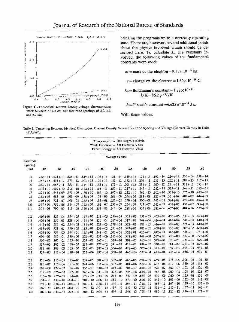
Journal of Research of the National Bureau of Standards
UF
E
T
DE:
AI2
CJIRRE IT 0E1ls IT US. UOLI LOE T- 300. E .5 Uf 4. 5
D-2.0
.0±0
.005 X
0.00 X. CJ 2 E=; t.. 35 .0 00.G 0.1 9.2 2.7 9 .1 J., 9.5 9.7
UOLTAGE t*OLT51
Figure 11-Theoretical current density-Noltage chtracteristics;work function of 4.5 eV and electrode spacings of 2.0, 21,and 2.2 nam.
bringing the programs up to a correctly operatingstate. There are, however, several additional pointsabout the physics involved which should be de-scribed here. To calculate all the constants in-volved, the following values of the fundamentalconstants were used:
m =mass of the electron=9.11 X 10-' kg
e =charge on the electron= 1.60X 10` 9 C
kz=Boltzmann's constant= 1.38X 10-x3J/K=86.2 geV/K
h =Planck's constant=6.625X 10i-4 j S.
With these values,
Table 2. Tunneling Between identical Electrodes: Current Density Versus Electrode Spacing and Voltage (Current Density in Units
of A/ni 2).
Temperature = 300 Degrees KelvinWork Function = 5.0 Electron Volts
Fermi Energy = 5.5 Electron Volts
Voltage (Volts)FlectrodeSpacing
mmi .05 .10 .15 .20 .25 .30 .35 .40 .45 ,50 .55 .60
.3 .212+13 .424+13 .636+13 .849 +13 .106+ 14 .128+14 .149+14 .171 + 14 .192+14 .214 +14 .236+14 .258 +14.4 .257 + 12 .515+12 .773 -- 12 .103+13 .129+13 .155 + 13 .182+ 13 .208 + 13 .235+13 .262+13 .289+13 .317+13.5 .283 + 11 .5 6 7-, t .852+ 11 .114+12 .143+12 .112+12 .201 +12 .231 + 12 .260+12 .291 + 12 .321+12 .353+126 .304+10 .609+10 .916+10 .122+1 1 .154 +11 t185-i11 .217+11 .249+11 .282+11 .315- 11 .349+11 .383+11.7 .324+09 .648+09 .975 +09 .130+ 10 .164+10 .197+10 .232 + 10 .266-10 .302 + 10 .338+ 10 .375 + 10 .413-'10.8 .342+08 .685 + 08 .103+09 .138+09 .173 +09 .209+09 .246+D9 .283+09 .322 +09 .361+09 .402 +09 .444+09.9 .360+07 .721+07 .109 +08 .145+08 .183 +08 .221+0O .260+08 .300+08 .342 +08 .384+0 0 428 +08 .474+0O
1.0 .377 + 06 .756+06 .114+07 .153 + 07 .192+07 .233 + 07 .274+07 .317+ 07 .362+07 .408+ 07 .456+07 .506+071.1 .394+05 .790+05 .119+06 .160+06 .201+06 244+06 .288+06 .334+06 .382+06 .432+06 .484+06 .539+06
1.2 .410+04 .823 +04 .124+05 .167+05 .21 1+05 .256+05 .303 +05 .351+05 .403 +05 .456+05 .513 +05 .573 +051.3 .426+ 03 .856+03 .129+04 .174 +04 .220-04 .267+04 .317+04 .369+04 .424+04 .482+04 .544+04 .610+041.4 .442+02 .889+02 .134+ 03 .181+03 .229+03 .279 +03 .332-,03 .387+03 .446-03 .508+03 .576-03 .648+031.5 .458+01 .921+01 .139+02 . I BS +02 .238+02 .291+02 .347+02 .406 +02 .469+02 .536 +02 .609+02 .688 +021.6 .474+00 .954+00 .144+01 .195+01 .248+01 .303 +01 .362+01 .425 +01 .492+01 .565 +01 .644+01 .731+011.7 .490-01 .986-01 .149+00 .202+00 .257+00 .315 +00 .378+00 .444+00 .517 + 00 .596+00 .682+ 00 .777 +001.8 .506-02 .102-01 .155-01 .209-01 .267-01 .328-01 .394-01 .465-01 .543-01 .62S-01 .721-01 .25S-011.9 .522-03 .105-02 .160-02 .217-02 .277-02 .341-02 .411-02 .486-02 .570-02 .661-02 .763-02 .877-022.0 .538-04 .108-03 .165-03 .224-03 .287-03 .354-03 .428-03 .509-03 .598-03 .697-03 .808 -03 .933-032.1 .554-05 .112-04 .170-04 .232-04 .297-04 .368-04 .446-04 .532-04 .62S-04 .735-04 .856-04 .993 -04
2.2 .570-06 .115-05 .175-05 .239-05 .308-05 .382-05 .465-05 .556-05 .659-05 .775-05 .906-05 .106-042.3 .586-07 .118-06 .181-06 .247-06 .319-06 .397-06 .484-06 582-06 .692-06 .817-06 .960-06 .112-052.4 .603-08 .122-07 .186-07 .255-07 .330-07 .412-07 .504-07 .608-07 .726-07 .862-07 .102-06 .120-062.5 .619-09 .125-OS .192-08 .263-08 .341-08 .428-08 .525-OS .636-08 .763-08 .909-08 .108-07 .128-072.6 .626-10 .129-09 .19S-09 .272-09 .353-09 .444-09 .547-09 .665-09 .802-09 .960-09 .115-OS .136-082.7 .654- 11 .133-10 .204-10 .281 - 10 .366-10 .461-10 .570-10 .696-10 .842 - 10 .101 -09 .122-09 .145-092.8 .671-12 .136-11 .210-I .289-11 .378-11 .479-11 .594-11 .728-11 .886-11 .107-10 .129-10 .155-102.9 .689-13 .140-12 .216-12 .299-12 .391--12 .497-12 .619-12 .762-12 .931-12 .113- 11 .137-11 .166-113.0 .707-14 .144-13 .222-13 .308-13 .405 -13 ,516-13 .646-3 .79S-13 .9MO-13 .120 - 12 .146-12 .177-12
193

Journal of Research of the National Bureau of Standards
Tlae 3. Tunneling Between Identical Electrodes; Current Density Versus Electrode Spacing and Voltage. Calculated from SimmonsTheory (Corrected). (Current Density in Units of A/m2 ).
Temperature = 300 Degrees KelvinWork Function = 5.0 Electron Volts
ElectrodeSpacing
(nm)
Voltage (Volts)
.05 .10 .15 .20 .25 .30 .35 .40 .45 .50
.3 -. 704+12 -. 142+13 -. 216+13
.4 .101 + 12 .204+12 .308+12
.5 .182+11 .367+11 .556+11
.6 .236+10 .478+10 .725+10
.7 .279+09 .564+09 .S56+09
.8 .3 14+08 .636+08 .966+08
.9 .345+07 .69S+07 .106+081.0 .372+06 .755+06 .115+07L11 .398+05 .507+05 .123+06
1.2 .421+041.3 .444+031.4 .465+021.5 .486+011.6 .506+001.7 .526-011.8 .545-021.9 .565-032.0 .584-042.1 .603 - 05
2.2 .621-062.3 .640-072.4 .659-082.5 .678-092.6 .697- 102.7 716- 112.8 .735- 122.9 .755- 133.0 .774-14
.855+04
.901 ±03
.946+02
.988+01.103+01107+00.111-O0.115-02.119-03.123-04
.127-05
.131 -06-135-07
-139-08
.143-D9
.147- 10
.151- 11
.155- 12
.159- 13
.130+05
.138+04
.144+03
.151+02.158 +01.164+00.170 -01.177-02.183 -03.189-04
.196-05
.202 -06
.208-07
.215-08
.221 -09
.228- 10
.235-l1
.242-12
.249-13
-. 292+ 13.413+12.749+ 11.978+ 10,I16+ IC).131+09.144+ 08JtS6 07.167+06
.177+05
.187+04
.197+03
.206+02
.215+01
.224+00
.233 -01
.242-02
.251 -03
.260-04
.270 -05
.279 -06
.282 -07
.298 -08
.307-09
.317 - 10
.327-Il
.338- 12
.348- 13
-. 371 + 13.520+ 12.946+11.124+ 11.146+10.166+009.13+08.198+07.212±06
.226 + 05
.239+04
.251-+-03
.264+ 02
.276+01
.228 -00
.300-01
.313-02
.325-03
.337-04
.350-05
.363-06
.376-07
.389-08
.403 -09
.417- 10
.431-11
.446- 12
.461 - 13
-. 452+ 13.62 + 12.115+ 12.150+1E.17S+ 10.202 + 09.223 +08.242 + 07.260+06
.277+05
.293 + 04
.309+03
.3 25 + 02
.341 +01
.357+00
.373 -01
.389-02
.405 -03
.422-04
.439 - 05
.456- 06
.474- 07
.492-08
.51 z -09
.530- 10
.550- 1 1
.571-12
.592- 13
-538+ 13.738+ 12.135+12.178+ 11.211 +10.239+09.265+08.288+07.310+06
.331+05
.351 +04
.371 +03
.391 +02
.411 +01
.431+00
.451 -01
.472 -02
.493 -03
.515-04
.537-05
.560-06
.584-07
.608 -08
.634-09
.660-10
.687-11
.716-12
.746- 13
-. 627+ 13.849+ 12.156+ 12.206+ 11.245 + 10.278+09.308+08.336+07.362+06
.387+05
.412+04
.437+03
.461 +02
.486+01
.511 +00
.537-01
.563-02
.590-03
.618-04
.647-05
.677 -06
.708-07
.741-08
.775-09
.810-IO
.847 - 11
.886- 12
.927 - 13
-. 721+13.962+ 12.178+12.235 + It.280+ 10.319+09.354+08.386+07.417+06
.447+05
.477+04
.507+03
.537+02
.568+01
.599+00
.631-01
.664-02
.698- 03
.734- 04
.771- 05
.810-06
.851-07
.894-0S
.939-09
.986- 10
.104- 10
.109- tl
.114- 12
-. 821+ 13.108+ 13.200+12.265+11.316+10.361 +09.401 +08.439 + 07.476+06
.511+05
.547+04
.583 +03
.619+02
.656+01
.695+00
.735-01
.776 -02
.819-03,865-04
.912-05
.962 -06
.101-06
.107-07
.113-08.119-09.126- 10.133- 11.140- 12
N(E,)=1.3585X 0O1 0Tln [ ] A/eV Km 2 .(2-78)
The values of a=10.25(eV)-> 2 (nm)-' and I.15e2
ln2/(87rE)=0.2867 (eV nm) were also obtainedwith these values for the fundamental constants.
Due to the nature of N(E.), which was ex-plained earlier, eq (2-61a) was decomposed intothree parts:
S-c-WV
Jj=A7kBT3 T(eV/ksT)jf
AF+T 3F-ETOPI =~kT S rE-,-eV
D(E.)dEi1,(2-79a)
EFp+SO/<T
J3==A Tk1 T L*F WY-STOP In(FD l/FD lI~dE
with J=J 1 +JL+J3 . c was chosen as 40k3 T andETOP is the top of the barrier potential function.Neglecting small changes in the maximum barrierheight with applied bias voltages, ETOP is givenby
ETOP=[0.575 e2In 2/(8ii-cflS-'. (2-80)
J3 was not included in the calculations unlessETOP was less than (Ep+80k7T).
The form for D(E;) used in the calculations wasJR
D(Ex) =(I1+exl[21 KI(xwdx])-'I, (2-8 1)
(2-79b) K(x) is defined in eq (2-61e). This form may beapproximately obtained from eq (2-61e) by factor-ing 4e2 from the second term and performing a
(2-79c) series expansion. The result is D(EJ)=(1/2+e 2 )-'.
194
ln(FDl1FDII)dE,,

Journal of Research of the National Bureau of Standards
Equation (2-81) has been obtained by Miller andGood 152] by analytic continuation and was shownto hold for all energies, including energies greaterthan the barrier height; one determines complexturning points in this instance. The Miller andGood form of the WKB transmission enabled thecalculations to proceed smoothly up to the top ofthe barrier, where XL=XR and D(E.)=0.5. Thevalue for the exact transmission coefficient of aparticle with energy at the top of a rectangularshaped barrier is 0.2. Since one would expect theimage potential rounded barrier to be less reflec-tive, the 0.5 value is at least intuitively correct. Toavoid the complexities of determining complexturning points, a simple linear interpolation be-tween 0.5 and I was used from ETOP to the vac-uum level.
Current Calculations for Spherical Electrodes4
Current flow was obtained from the current den-sity calculations by assuming that in the almost pla-nar electrode structure, the current flow wasparallel to the axis of the two spheres. The incre-mental tunneling areas are then rings around thisaxis of radius r with spacing greater than the clos-est spacing between the electrodes. The currentflow in this approximation is
I= J(x)dA, (2-82)
J(x) is the current density for an electrode spacingx, xO is the on-axis electrode spacing and x. is thespacing between points off-axis at which J(x) hasdropped to a negligible value. For r much smallerthan the sphere radius R,
4The high lateral resolution implied by the imaging of the Si(III) surface obtained by G. Binnig, H. Rohrer, Chi. Gerber,and E. Weibel (Phys. Rev. Lett. 50 (1983) 120) has stimulatedmuch theoretical investigation of the effect of electrode shapeon the tunneling current and effectiw tunneling area. Thestrong exponential dependence of the tunneling current on elec-trode spacing tends to confine the tunneling current to verysmall regions of one of the electrodes if it is sharpened. Some ofthe investigations of the shape of the electrodes on the tunnelingcurrent and tunneling area are: N. M. Miskovsky, S. J. Shep-herd, P. H. Cutler, A. A. Lucas, and T. E. Sullivan, Effect ofGeometry and Multiple Image Interactions on Tunneling andI-V Characteristics of MVM Point-Contact Junctions, App.Phys. Lett. 3X (1980) 189; 1. Tersoff and D. R. Hamann, Theoryand Application for the Scanning Tunneling Microscope, Phys.Rev. Lett. 50 (1983) 1998; N. Garcia, C. Ocal, and F. Flores,Model Theory from Scanning Tunneling Microscopy: Applica-tion to Au (11O)(lX2), Phys. Rev. Lett. 50 (1983) 2002; T. E.Feuchtwang, P. H. Cutler, N. M. Miskovsky, Theory of Vac-uum Tunneling Microscopy, Phys. Left. 99A (1983) 67; A.Baratoff, Theory of Scanning Tunneling Microscopy - Methodsand Approximations, Physica 127B (1984) 143.
r(x)= [R (x -xo)]`.
With dA =2Irrdr, eq (2-82) is therefore
I=7rR f J(x)dx.
(2-83)
(2-84)
The 10-" factor employed in the programs in Ap-pendix I results from the use of x in nm and R inmm.
3. Experimental Apparatus and Method
The rule-of-thumb expression for the tunnelingcurrent 1, at small voltage, V
I=C exp(-aSB1 )A V, (3-1)
and its ramifications are the major factors whichdetermine all aspects of the apparatus design, con-struction, and use of apparatus for metal-vacuum-metal tunneling. C is a constant, A is the devicetunneling area, a is 10.25 (eV)-' (nm)-1 , S is theelectrode spacing, and B is the mean barrier height.Some insight into the experimental problems whichhad to be addressed may be obtained by observingthat according to eq (3-1) a change in electrodespacing of 0.1 nm, about one-half an atom diame-ter, will generate a factor of 10 change in the tun-neling current, assuming a barrier height of 5 eV.In a metal-vacuum-metal tunneling device, an elec-trode spacing stability of one pm is therefore re-quired to achieve a noise level of 2% or less in thetunneling current for a fixed voltage. This corre-sponds to a signal-to-noise ratio of only 34 dB.
Mechanical and Thermal Requirements
The electrode spacing stability is in turn deter-mined by the mechanical and thermal properties ofthe electrodes and the assembly into which theyare placed. As representative values, let the effec-tive length, L, for thermally generated changes inelectrode spacing be 5 mm and the expansion coef-ficient, kT, of the materials involved be 10 ppm/K.Then, the required temperature stability, dT, toachieve a 1 pm stability, dL, in electrode spacing is
dT=dL(L kr)- =20 AK (3-2)
The laboratory in which the experiment was to beperformed had a temperature stability of ±0,5 Kover a 24-hour period. However, when localsources of heat such as that of the body heat of theexperimenter are taken into account, the local vari-
195

Journal of Research of the National Bureau of Standards
ations in environmental temperature are more rep-resented by ± I K. An approximate attenuation of10' of the environmental temperature variationsmust, therefore, be provided by a temperature con-trol system.
Requirements for mechanical stability were de-termined by measuring the amplitude and fre-quency composition of building vibrations at theplanned laboratory location of the experimental ap-paratus. The transducer used for these measure-ments was a Texas Instruments S-36 very lowfrequency seismic detector whose sensitivity was1.97 V/cm/s. The transducer's response was ap-proximately 10% greater at its resonance fre-quency of 2 Hz and dropped by about 15% at I Hz.Figure 18 shows the velocity amplitude spectrumof the building vibrations in the National Bureau ofStandards Reverberation Chamber. Measurementswere performed here because it was one of the qui-etest potential locations for conducting the vacuumtunneling experiment. In addition, it was the onlylaboratory which allowed convenient access to theFourier transform electronics necessary for obtain-ing real-time vibration spectra. Vibration spectrafrom this location were compared with other possi-ble locations for the experiment with the use ofoscillographs. These oscillographs showed that thevibrations present on a vibration table with a reso-nant frequency of 1 Hz and located in a basementlaboratory were similar in amplitude and frequencycontent to those measured in the well-isolated NBSReverberation Chamber. The NBS ReverberationChamber is a room-within-a-room structure withan inside room volume of about 400 m3 . The innerroom is supported on springs to produce a room-spring resonance frequency of 3.5 Hz.
Depending on the frequency, the vibration am-plitudes which must be accounted for, even with a
vibration isolation table, are therefore between 4and 25 nom. The amplitudes are deduced from fig-ure 8 with the 25 nm amplitude corresponding tofrequencies of about 3.5 Hz, and the 4 mmr to a fre-quency of about 35 Hz. Figure 18 only shows thevertical component of vibration displacements;measured horizontal components were similar inamplitude, but with major contributions existingonly at frequencies near 35 Hz and below 10 Hz.The mechanical design of the electrode holdermust, therefore, attenuate these vibrations by about10'- to produce the I pm stability.
A second factor which must be accounted for indesigning for mechanical stability is acousticalpressure variations in the air around the experimen-tal apparatus. No measurements of the magnitudeand frequency content of the acoustical pressurevariations were made since reliable estimates couldbe obtained from the literature. Hunter [53] gives agraph of the noise amplitude as a function of fre-quency for an average room. For a mean noiselevel of 40dB referenced to 2 iX-5 N/m 2 , the am-plitude at 20 Hz was 40 dB and dropped almostlinearly to -5 dB at 5000 Hz. Within the labora-tory used for this experiment, there were no dis-tinctive noise sources, so this description of theacoustical environment was taken as representa-tive.
Choosing an Electrode Material and Preparing theElectrodes
Variations in the mean barrier height also pro-duce large changes in the tunneling current. Forsmall changes in B, dB, eq (3-1) may be used toobtain
dk/I= -1/2 a S B ,' dB. (3-3)
Figure 18-Measured velocity am-pbtude spectrum of building vi-brations in the Naticnal Bureauof Standards ReverberationChamber.
E
-aLUa
0.
4
0-LJ
w:
a.,
FREQUENCY (Hz)
196

Journal of Research of the National Bureau of Standards
With 5=1 nm, B=4 eV, and dB=0.I eV, dIl= -0.26, B must be stable to 0.008 eV to achieve a34 dB signal to noise ratio.
Changes in work function and thus barrierheight are produced by the adsorption andchemisorption of any kind of foreign atom on ametal surface [27,32]. The change in the work func-tion WF, WFC, is a local microscopic effect, but interms of a spatially averaged change, it can for-mally be related to an effective dipole moment pper adsorbed particle via the equation [32,54]
WFC=4p N, (3-4)
where N is the number of adsorbed atoms ormolecules per unit area. Adsorption is viewed aschanging the [V(+ C)- V(- c)] term of the WEdescribed in section 2. Changes in WF range from+0.08 eV for a 1/3 monolayer of selenium onnickel to -3.1 eV for a monolayer of cesium ontungsten (100) [32,54]. Larger increases in the WFare also found, but usually no greater than I eV.WFC's due to more common adsorbates such asoxygen, nitrogen, and hydrogen are typically aboutI eV, and may be of either sign depending on thesubstrate-adsorbate combination.
This demand for stable clean electrode surfacesmust be carefully balanced with the opposing needfor high temperature stability. There are two majorreasons for the conflict between these two require-ments. First, to achieve atomically clean metal sur-faces, such that the work function would not bechanged by any contaminants, some form of in-situvacuum cleaning process must be employed. Themost common and reliable methods for in-situcleaning all require large energy inputs either tosimply evaporate or decompose all surface andnear surface contaminants, e.g., high temperatureflashing of W or high temperature cycling in oxi-dizing and reducing atmospheres, e.g., Ni in 0, andH,. Second, the time for a contaminating layer toform on a clean surface is comparable with esti-mated times for an electrode assembly to thermallyequilibrate to the stabilities demanded by the vac-uum tunneling experiment.
The time, T, in which an initially clean surfacewill become covered with a monolayer of adsor-bate when the surface is exposed to a gas at pres-sure P Torr is (see Appendix III)
T_2X 1061P seconds. (3-5)
Equation (3-5) is only a rough estimate, but it isuseful in determining the vacuum conditions neces-sary for this particular application. A minimum
time for a system that has been raised to 1300 K toobtain a 10 1 K stability is about 24 hours or8.6X 105 seconds. Thus, maintaining a clean surfaceover this period of time would require that the par-tial pressures of all possible adsorbates be less than1012 Torr. Vacuum pressures at this level are atthe limits of modern technology and are achievedwith only cryopumping or by very careful use ofvacuum materials.
As a compromise between the demands of tem-perature stability and the requirement for clean sur-faces, gold was chosen as the electrode materialbecause none of the common adsorbates, includingmolecular oxygen, have been found to chemisorbat room temperature and it could be convenientlyformed into electrodes with clean, smooth surfacesprior to installation into the temperature controland micropositioning assembly.
The approach taken was to fabricate the goldelectrodes in one UHV system, to store and trans-port the fabricated electrodes in desiccated con-tainers, and finally to assemble the electrodes intoan electrode assembly in the laboratory atmo-sphere. As discussed in the next paragraph, thisprocedure certainly does not result in an ideallyclean surface. However, after the electrodes areplaced in a UHV environment, the surfaces shouldbe altered by at most a monolayer of hydrocarbonand require no further processing before the vac-uum tunneling experiment could reliably be per-formed at a stable temperature.
The most definite study of gold's resistance toadsorbing molecular species was performed byChesters and Somorjai [55]. They found that of thespecies most likely to be encountered in a labora-tory environment, oxides, sulphides, hydrocarbons,nitrides, and water vapor, the only ones whichwere observed to adsorb on a gold (111) crystalface or a stepped crystal face were heavy hydro-carbons. Their investigations were with the crys-tal's temperature less than 500 'C and partialpressures less than 106 Torr. Naphthalene ad-sorbed on both types of gold surfaces and the ad-sorption behavior indicated dissociativechemisorption. Surface steps did not play a criticalrole in the adsorption properties of gold, in con-trast to that of the similar chemical material, plat-inum. Earlier work by Trapnell [56] usingpolycrystalline gold films showed that reversiblemolecular adsorption of CO, CQH4, CH,, and otherlight hydrocarbons did occur with low heats of ad-sorption (0.4 eV/molecule) for high pressures.These low heats of adsorption allow the adsorptionprocess to be reversible and Trapnell [56] showsthat at low pressures and room temperature, the
197

Journal of Research of the National Bureau of Standards
light hydrocarbons desorb with no measurable, i.e.,less than 2% coverage at pressures less than 10'Torr.
Work function changes, WFC, in gold due toadsorption have received very little study, in partbecause gold is the most common reference elec-trode for measurements of the work function [32].In particular, no work to determine the WFC's dueto the adsorption of heavy hydrocarbons wasfound in the literature. However, WFC's in plat-inum have been studied for a wide variety ofmolecular species. While the type and behavior ofmolecular species which adsorb on gold surfaces ismarkedly different from that on platinum surfaces,the WFC's observed in the studies of adsorption onplatinum at least set an upper bound on the WFC'sto be expected for adsorption on gold. The valuesof the WFC's of the platinum do reflect the effec-tive dipole moments of the adsorbed molecules ona dominantly s-electron like surface and shouldgive a valid estimate of the dipole moment of themolecule when it is adsorbed on gold. The major
Figure 19-Apparatus for formingthe gold electrodes.
difference between platinum and gold from thestandpoint of chemical properties is that platinumhas an unfilled 5d electronic subshell. For plat-inum, the WFC's were measured by Gland and So-morjai [57] for a wide range of heavyhydrocarbons. WFC's were found to be between-1.0 and -2.0 eV depending on the type of adsor-bate and the degree of coverage of the platinumsurface.
The gold electrodes were formed by melting theend of a 1.25 mm gold wire in UHV with electronbombardment. The apparatus used for forming theelectrodes is shown and described in figure 19.Gold wire with 99.99% purity was used. Follow-ing degreasing with a trichloroethylene, acetone,ethanol sequence, the wires were etched in boilingaqua-regia, i.e., 3.5 parts HCO and I part HNO,;both acids were fresh ACS grade chemicals. Afterrinsing the wires thoroughly in running tap water,they were ultrasonically cleaned in de-ionized, fil-tered water and finally blown dry with hot air. Thewires were then installed in the electron bombard-
/ ~~~1.25 MM D. NICHROMF WIRE
6 MM D. X 2 CM H.
/ESMAM EhO RESISTANCE
OLD WIRE FOR FORMINGONE ELECTRODE1.25 MM D. X 5 CM LONG
-0.5 Ml D. TUNGSTEN
FILAMENT
4-1'IO V.
10:1 STEPDOWN
I I 511 120 VAC
198

Journal of Research of the National Bureau of Standards
ment apparatus and vacuum pumping was begun.The vacuum system used for the melting opera-
tion utilized a sublimation-ion pump combinationwhich maintained pressures of 2 to 4 X 10' Torrwhile the gold was molten. With the 1.4 kV indi-cated in figure 19, only about 15 mA of bombard-ment current was required to melt the end of a goldwire.
The stainless steel mass-thermal resistance is anessential component of the melting apparatus. Thiscomponent combined with the nichrome wire pro-vides sufficient thermal resistance to allow an equi-librium between input and dissipated power to beobtained by convenient manual adjustment of thefilament heating current. Without these compo-nents, the equilibrium is difficult to obtain; thenonequilibrium result in this case is that the moltenregion of the wire moves up the length of the wire,forms a sphere and drops off the wire. Aftdri sev-eral of these occurrences, the configuration shownin figure 19 was developed to avoid this problem.With this design, a molten sphere could be main-tained on the end of the wire with the support ofthe liquid's surface tension for 10 to 20 minutes.These long periods in the molten state in vacuumprovided a means to evaporate many contaminantsfrom the surface and were sufficient for the surfacetension forces to determine the microscopic surfacetopography.
After melting, the electrode surfaces were in-spected with an optical microscope at a magnifica-tion of 300X. The process from etching in aquaregia to melting was then repeated until no surfacecontamination was visible. For the pair of elec-trodes used in the experiment, the process was re-peated four times. The resulting surfaces were verysmooth with no visible topography or contami-nants. The electrodes were finally examined with ascanning electron microscope (SEM) after the ex-periment was completed. The SEM micrographs ofthe electrode surfaces are shown in figures 20 and21. The surfaces were sufficiently smooth that inboth the electron and optical microscopes good fo-cus was difficult to obtain.
The anticipated electrode surfaces for this exper-iment were, therefore, clean gold surfaces alteredby at most a monolayer of adsorbed heavy hydro-carbons to produce work functions which couldrange from gold's work function, 5.0 eV, down to aminimum of 3.0 eV.
Temperature Control System
In order to provide the required stability of +±1pm for the interelectrode spacing, the design goal
Figure 20-Scanning-electron-microscope photomicrograph ofgold electrode surface; view normal to surface.
Figure 21-Scanning-electron-microscope photomicrograph ofgold electrode; surface projection.
for the temperature control system was to producea temperature stability of ±+20 tK. Other workers[58,59] have shown that by careful design, temper-ature stabilities at this level can be achieved withthe use of a two-stage control system. This ap-proach was therefore adopted. The first and outerstage was designed to operate at a temperature of 5K above the laboratory temperature with a stabilityof +1 ImK. The second and inner stage was de-signed to operate at a temperature 0.5 K above the
199

Journal of Research of the National Bureau of Standards
outer stage's temperature with the specified designgoal stability.
The apparatus used for the combined purposes oftemperature control, vibration isolation, and acous-tical isolation is shown and described in figure 22.Vibration and acoustical isolation aspects of the ap-paratus are described in a later section. Several fea-tures of this apparatus should be emphasized: 1)Bifilar windings were used for both control heatersto insure that stray magnetic fields in the region ofthe electrode assembly would be minimal. 2) Radi-ation baffling was provided at the vacuum pump-ing part of the inner heater enclosure to minimizethe radiant coupling between the outer heater'sfluctuations and the electrode assembly. The baffledesign insures that any radiation entering thepumping port must be scattered at least five timesfrom the surface of the inner heater enclosure. 3)All joints in the polyurethane insulation and open-ings for the various vacuum parts were taped with
Figure 22-Apparatus for vibration isolation, acous-tical isolation, and temperature control, consist-ing of the following components: I) Electrodeholder and micropositioning assembly. These aredescribed in figure 25. 2) Inner stage temperaturecontrol enclosure (6061 Aluminum) and heater.The heater wires shown are only schematic, ac-tual wires were of #30 nichrome in a bifilar con-figuration which almost completely covered the (enclosure's cylindrical surface. The radiation baf-fle is the cross-hatched piece located immediatelyabove the electrode assembly. 3) Aluminum (6061alloy) base for inner enclosure 4) Alumina stand-offs. Three were used to provide thermal isola-tion between the two temperature control stages.5) Outer stage temperature control enclosure,heater and vacuum chamber walls. The cylinderwall thickness was 3.2 mm, top and bottom thick-nesses were 1.9 cm. Heater wires were #31 cop-per spaced approximately as indicated in thedrawing. An epoxy coating approximately 3.0mm thick with a thermal conduction coefficient Xof 0.01 (cal cm)/(sec cm2 'C) [60], was used to -
bond the heater wires to all surfaces of the outer .
enclosure and to provide acoustical damping. 6) 8 _cm thick polyurethane foam. This foam provided Xboth thermal and acoustical isolation of the sys-tem enclosure and 7) Epoxy standoffs, three,were used to provide thermal insulation of outerenclosure and vacuum system from the vibration .
isolation table. These standoffs were bonded tothe vibration isolation table top and permittedrigid coupling of the entire apparatus to the isola-tion table top. And 8) Granite isolation table. Thetable was 61 cmX 25 cm and had an approximatemass of 409 kg. It was supported with fourdamped steel springs from a simple aluminumframe. The resonant frequency of the system wasless than I Hz for vertical motion.
building construction duct tape to minimize con-vection losses. 4) Electrical leads passing from thelaboratory through the first stage and from the firststage through the second stage to the electrode as-sembly were in both cases solidly heat-sunk to theenclosure of each respective stage. For the outerstage, thermal contact for each electrical lead wasobtained by soldering one point of the lead to acopper post which was mounted to the outer en-closure with the same high thermal conductivityepoxy used to mount the heater wires; see figure22. Thermal contact for leads passing through theinner stage enclosure was obtained by using copperfeed-throughs in the base of the enclosure, item 3 infigure 22, which were electrically insulated withberyllium oxide washes. Total contact area foreach lead was 3 cm2 .
A block diagram of the temperature control sys-tem employed for both control stages is shown infigure 23. The basic design approach of both stages
200
I , 10 cm-I - -d

Journal of Research of the National Bureau of Standards
T (ENVIRONMENT)
Figure 23-Block diagram of temperature control electronics.
was to use the output of a bridge to drive a highgain amplifier and compensation network to ac-count for the lags of the detectors and stage-masses, then to close the control loop byincorporating a thermistor detector as one elementof the bridge. A full discussion of the electronics ofboth control stages is given in Appendix V. Thereit is shown that one of the most important parame-ters of the control loop is the time response of thethermistors with respect to changes in power inputto the heaters. For this reason, the thermistorswere mounted in a manner to allow the closest pos-sible coupling between the heaters and the thermis-tors.
The principal difference between the two stagesof temperature control was that a dc bridge and asensor amplifier were used for the outer stagewhile an ac excited bridge and lock-in amplifierwere used for the inner stage. The compensation
OYERPRESSURE
RELEAS XXX SORP
Xxx PUMP
FORELINEVALVE
THERMOCOUPLE
UP-TO-AlIVALVE
GOLD SEALUHV VALVECONDUCTANCEFULL OPEN 1O L/S
network, power amplifier and heaters were tai-lored for the requirements of each stage. Values forthe heat capacities, thermal resistances, and massesof each stage are given in Appendix V.
Both controllers were designed to allow conve-nient and accurate changes in operating tempera-ture. The outer stage's setpoint could be changedin 2 mK increments with the use of a switched re-sistor network. Setpoints for the inner stages werechanged with a seven-digit ratio transformer whichpermitted 10 FtK increment changes.
Performance of the outer control stages waschecked by using the inner stage detector system asa temperature monitor. When this stage's compen-sation network was adjusted as described in Ap-pendix V, temperature deviations from thesetpoint, measured over a 10-hour period, were nogreater than ±0.5 mK. The only check on the in-ner control stage's performance was to monitor thestability of the interelectrode spacing. The resultsof this check are given in section 4 where it isshown that no changes in electrode spacing due totemperature variations were observed. A major in-dication of the sensitivity of the inner stage con-troller was that a setpoint change of 30 pK wouldcause an observable change in the output of thisstage's sensor amplifier. The response of bothstages to setpoint changes is described in AppendixV.
Vacuum System for the Tunneling Experiment
A schematic diagram of the vacuum system usedfor the tunneling experiment is given in figure 24.
TION
TITANIUM SUBLIMATION PUMP
BAYARD-ALPERT
ITYPE IONIZATION GAUGE
TRIODE ION VACUUMPUMP 20 L/S
Figure 24-Schematic diagramtunneling experiment.
of vacuum system used for the 20 PIN ELECTRICALFE EDT HRO UGH
201
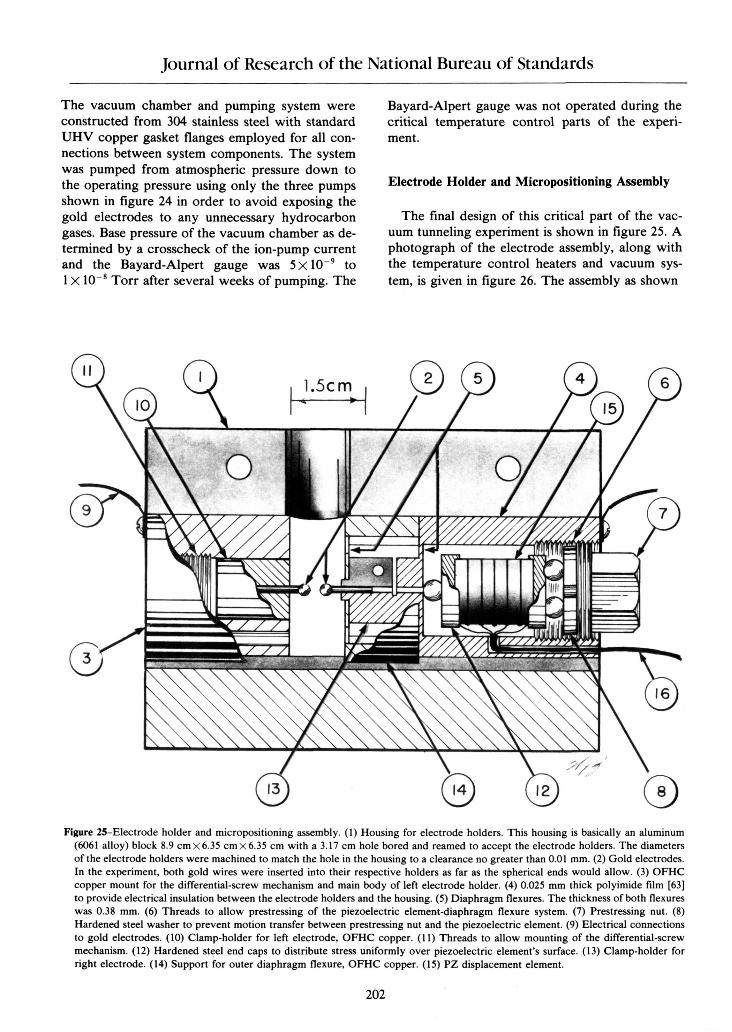
Journal of Research of the National Bureau of Standards
The vacuum chamber and pumping system wereconstructed from 304 stainless steel with standardUHV copper gasket flanges employed for all con-nections between system components. The systemwas pumped from atmospheric pressure down tothe operating pressure using only the three pumpsshown in figure 24 in order to avoid exposing thegold electrodes to any unnecessary hydrocarbongases. Base pressure of the vacuum chamber as de-termined by a crosscheck of the ion-pump currentand the Bayard-Alpert gauge was 5 X 10-9 toI X 10' Torr after several weeks of pumping. The
Bayard-Alpert gauge was not operated during thecritical temperature control parts of the experi-ment.
Electrode Holder and Micropositioning Assembly
The final design of this critical part of the vac-uum tunneling experiment is shown in figure 25. Aphotograph of the electrode assembly, along withthe temperature control heaters and vacuum sys-tem, is given in figure 26. The assembly as shown
Figure 25-Electrode holder and micropositioning assembly. (I) Housing for electrode holders. This housing is basically an aluminum(6061 alloy) block 8.9 cmX6.35 cmX 6.35 cm with a 3.17 cm hole bored and reamed to accept the electrode holders. The diametersof the electrode holders were machined to match the hole in the housing to a clearance no greater than 0.01 mm. (2) Gold electrodes.In the experiment, both gold wires were inserted into their respective holders as far as the spherical ends would allow. (3) OFHCcopper mount for the differential-screw mechanism and main body of left electrode holder. (4) 0.025 mm thick polyimide film [63]to provide electrical insulation between the electrode holders and the housing. (5) Diaphragm flexures. The thickness of both flexureswas 0.38 mm. (6) Threads to allow prestressing of the piezoelectric element-diaphragm flexure system. (7) Prestressing nut. (8)Hardened steel washer to prevent motion transfer between prestressing nut and the piezoelectric element. (9) Electrical connectionsto gold electrodes. (10) Clamp-holder for left electrode, OFHC copper. (II) Threads to allow mounting of the differential-screwmechanism. (12) Hardened steel end caps to distribute stress uniformly over piezoelectric element's surface. (13) Clamp-holder forright electrode. (14) Support for outer diaphragm flexure, OFHC copper. (15) PZ displacement element.
202
"710�I
106
(D
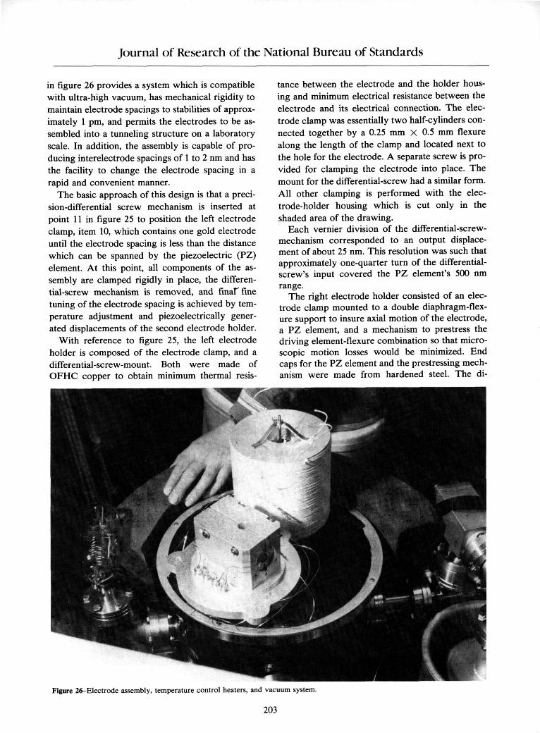
Journal of Research of the National Bureau of Standards
in figure 26 provides a system which is compatiblewith ultra-high vacuum, has mechanical rigidity tomaintain electrode spacings to stabilities of approx-imately 1 pm, and permits the electrodes to be as-sembled into a tunneling structure on a laboratoryscale. In addition, the assembly is capable of pro-ducing interelectrode spacings of 1 to 2 nm and has
the facility to change the electrode spacing in a
rapid and convenient manner.The basic approach of this design is that a preci-
sion-differential screw mechanism is inserted atpoint 11 in figure 25 to position the left electrodeclamp, item 10, which contains one gold electrodeuntil the electrode spacing is less than the distancewhich can be spanned by the piezoelectric (PZ)element. At this point, all components of the as-sembly are clamped rigidly in place, the differen-tial-screw mechanism is removed, and finar finetuning of the electrode spacing is achieved by tem-perature adjustment and piezoelectrically gener-ated displacements of the second electrode holder.
With reference to figure 25, the left electrodeholder is composed of the electrode clamp, and adifferential-screw-mount. Both were made ofOFHC copper to obtain minimum thermal resis-
tance between the electrode and the holder hous-ing and minimum electrical resistance between theelectrode and its electrical connection. The elec-trode clamp was essentially two half-cylinders con-nected together by a 0.25 mm X 0.5 mm flexurealong the length of the clamp and located next tothe hole for the electrode. A separate screw is pro-vided for clamping the electrode into place. Themount for the differential-screw had a similar form.All other clamping is performed with the elec-trode-holder housing which is cut only in theshaded area of the drawing.
Each vernier division of the differential-screw-mechanism corresponded to an output displace-ment of about 25 nm. This resolution was such thatapproximately one-quarter turn of the differential-screw's input covered the PZ element's 500 nmrange.
The right electrode holder consisted of an elec-trode clamp mounted to a double diaphragm-flex-ure support to insure axial motion of the electrode,a PZ element, and a mechanism to prestress thedriving element-flexure combination so that micro-scopic motion losses would be minimized. Endcaps for the PZ element and the prestressing mech-anism were made from hardened steel. The di-
Figure 26-Electrode assembly, temperature control heaters, and vacuum system.
203

Journal of Research of the National Bureau of Standards
aphragm-flexures and piezoelectric element wereprestressed with a force of approximately 890 N(200 pounds). All other parts of the electrodeholder, except the 304 stainless steel fasteners, weremachined from OFHC copper. The PZ elementwas electrically insulated from the rest of theholder with four sapphire spheres.
The PZ element consisted of six ceramic discs,each 1.27 cm in diameter by 0.25 cm thick. Theceramic was a barium-titanate-zirconate composi-tion which has very low hysteresis, linear charac-teristics [61]. The relevant expansion coefficient forthe material is d3 3 =225 pm/V for fields along thepoled direction of the ceramic; here perpendicularto the disc faces. The individual disks and end capswere bonded into one element with the use of alow viscosity, electrically conductive epoxy. Theepoxy's electrical resistivity was less than 0.002ohm-cm [51]. After baking in air at 100 0C for onehour, the outgassing rate was sufficiently low thatthe 10"'' Torr base pressure of a bell jar systemwith a 50 I/s ion pump was unaffected by the pres-ence of the epoxy bonded piezoelectric element.
Displacement characteristics of the completelyassembled micropositioning system were measuredbefore and after the tunneling experiments de-scribed in section 4. Before the experiments, thedisplacements were measured with a precise butuncalibrated mechanical gauge to be (.56± .06)nm/V. After the experiment, the displacementswere measured with a Hewlett-Packard 5526Alaser interferometer measurement system in combi-nation with a 10565B remote interferometer andretroreflector. This measurement system enableddisplacements to be measured with an accuracy of
9.1K
9.1K
±25 nm. For both expansion and contraction ofthe piezoelectric element, the displacements weremeasured as (0.47±.03) nm/V. Thus, taking intoaccount the uncalibrated state of the mechanicalgauge, the displacement characteristics of the mi-cropositioning system were stable throughout theexperiment.
The need for I pm electrode spacing stabilitycombined with the 470 pm/V sensitivity of the PZelement requires that the high voltage power sup-ply used to drive the PZ element have a very lowvoltage noise level, less than 2 mV. The power sup-ply used for this purpose had a noise level of lessthan 75 AV peak-to-peak and the capability of be-ing switched in I mV increments from - 1100 voltsto + 1100 volts [64]. To enable continuous voltagesweeps over ± 10 volts, a ramp generator wasadded in series with this power supply. The circuitdiagram of the ramp generator and a filter circuitto suppress switching transients are shown in figure27.
Two other experimental techniques for holdingand positioning the tunneling electrodes were thor-oughly explored before finally adopting the elec-trode holder and micropositioning assembly designjust described. The technique first explored was tofabricate the tunneling structure as a microelec-tronic device with the use of photolithographicmethods. This approach was not adopted becausethe technology to which the author had accesscould not meet the dimensional requirements of thetunneling device. However, as a byproduct of thiswork, the approach may result in an electronicdevice with a very high transconductance; valuesup to I mho appear feasible. A patent application
TOR_~
-100 5.-I
56M
0±1100 V.OUT
0.015
RAMP GENER. ~_ - IN MICA 2000,, M:
TO PIEZOELECTRIC DISPLACER Figure 27-Schematic diagram oframp generator and highvoltage power supply for thepiezoelectric element.
TE: ALL RESISTANCES IN OH1MS
ALL CAPACITANCES IN MICROFARADSLOW LEAKAGE CERAMIC
204

Journal of Research of the National Bureau of Standards
on the concept is being submitted to the NationalBureau of Standards Patent Review Committee.The concept and a prototype device are describedin Appendix IV.'
Lever amplification of the piezoelectric ele-ment's length changes was also explored as a possi-ble means to bridge the gap between laboratoryscale distances and the microscopic dimensions re-quired by the tunneling experiment. While thistechnique proved to have excessive vibration levelsfor the tunneling experiment, it has characteristicswhich are very useful for scanning-electron andoptical microscope stages [65].
Vibration and Acoustical Isolation
In the previous metal-vacuum-metal tunnelingexperiment [12] similar to this work and in all ear-11er attempts made in connection with this work,vibrations of the tunneling device structure at the Inm level have limited a successful execution of theexperiment. Every effort was made, therefore, tocarefully examine the mechanical design of eachpart of the apparatus to insure that all knownsources of vibrational energy were attenuated tolevels which would not result in detrimentalchanges in the electrode spacing. The vibrationalproperties of what was thought to be the mostlikely contributors to changes in electrode spacingwill now be described in terms of one-dimensionalmodels.
Starting with the electrode holder and micropo-sitioning assembly, the most likely contributor isvibrational motion of the right electrode holder asthe entire assembly is vibrated along the assembly'saxis. This motion could be produced either fromacoustical pressure variations on the bottom of thevacuum chamber or from building vibrations driv-ing the isolation table top and, thus, the entire vac-uum chamber. As a model of this motion, let amass, mi, be connected by a spring with force con-stant k, and a viscous damper characterized by theconstant C, to a vibrating wall whose displacementis given by xb=Ao sin cwt. Then the equation ofmotion of m in terms of x, measured relative to thewall is
mn (t+x + C* + kx = O. (3-6)
The steady state solution to eq (3-6) with the as-sumed form of x,, is
'A variation on the concept proposed here has recently beendeveloped by J. Moreland and J. W Elkin, Electron TunnelingExperiments Using Nb-Sn 'Break' Junctions, 1. AppI. Phys. 58(1985) 3888. They use a bending beam to produce and vary thespacing between electrodes.
x =R 2[(l -R )2 +4R1-" 2 lx,, (3-7)
R =a,/wo, &oo=(k/m)'`, and V= 1/2C(mk)->1 2 . If cois much less than coo, then
x=Rx 6,. (3-8)
Thus, if fib is the lowest resonant mode fre-quency of the micropositioning assembly for axialvibrations and the full amplitude of the isolationtable top's horizontal motion is transmitted alongthe axis to the electrode holder housing, fo(=wdo21r) must be greater than 6 kHz. This follows withthe use of an Xu of (27)30 radians/s, an x,,, of 40 nm,and a requirement that x be less than I pm. Theonly mechanical element with a resonant frequencynear this value is the diaphragm flexures, whichwere designed to have a resonant frequency of 10kHz, when unstressed. When stressed, the fre-quency would be even higher and motion wouldthen be determined almost entirely by the pre-stressing mechanism.
For motions normal to the axis of the assemblyall resonant frequencies are much higher than 10kHz. The relatively large gold wires were used toavoid low resonant frequencies in those directions.For example, even with a very high modulus ofelasticity material such as tungsten, the transversevibrational resonant frequency of a cantilever only2 mm long and .025 mm in diameter is 4 kHz [66].
To minimize the affects of any acoustically gen-erated vibrations, the electrode holder and micro-positioning assembly are only connectedmechanically to the laboratory environment by thebottom plate of the vacuum chamber. This plate isheavily damped both by the epoxy layer for attach-ing the heater wires and by the polyurethane foam.
The four lowest eigenfrequencies of the bottomplate are approximately: 884 Hz, 1.85 kHz, and 3.0kHz, and 3.5 kHz [66]. These neglect any massloaded decreases in the frequencies due to the massof the tunneling assembly, which is supported bythe plate and any increases in the frequencies dueto the epoxy damping. The lowest of these frequen-cies again is the most likely source of transmittingacoustical pressure variations to the electrode as-sembly. As a safety factor for design, a 40 dB whitenoise spectrum was assumed to exist up to one kHz,i.e., pressure variations, P.,,, with amplitudes of2X 10-' N/Mn2 . For frequencies much less than theeigenfrequencies, the vibrational amplitudes, Y, ofthe plate at the center of the plate would be [55]
Y=3P,,(t-s2 )a4 /(4tQ), (3-9)
205

Journal of Research of the National Bureau of Standards
s=Poisson's ratio=0.33, a=radius of the plate==.127 m, t=thickness of the plate= 1.9 cm, and Q=modulus of elasticity of the plate= 1.86X 10'°N/m2 . With the indicated P.,, Y is only 8.7 pm. Forfrequencies on resonance, the amplitudes of vibra-tion should be no larger than 10 times this valuewith the epoxy and polyurethane damping [67].Since the assumed pressure variations were largerthan expected and did not account for any attenua-tion due to the polyurethane foam, no further stiff-ening of the plate was performed.
Figure 28-Block diagram of tun-neling electronics.
Tunneling Electronics
The electronics used to measure the conductionproperties of the tunneling devices are shown infigures 28 and 29. Requirements of the electronicswere that it permit one to test devices whoseimpedances could range from 10-2 to 10" ohmswith dc test voltages of typically 10 mV. The de-sign shown in figure 28 utilized an operational am-plifier in a follower configuration to insure that,other than voltage drops in the current leads, the
I ~~~~~~~~~oP AMP
I TUNNELING OGAINo 2 X io5
I BIA SUPPL
T To-~1000 LX
l - ~~~~~~~~ms
L
DC VOLTMETER TO "X"OF
IIo±V L.C. RECORDER
OUTPUT A
(A)
PFILRRICK 4350 OR 4351LOG. AMP. MODULE
Figure 29-Schematics for compo-nents of the tunneling electron-ics. (A) Ramp generator forsweeping bias voltage. (B) Man-ual sweep and bias supply. (C)Logarithmic amplifier. (4)
(C)
NOTE: ALL RESISTANCES IN OHMSALL CAPACITANCES IN i ICROFARADS
206
-t

Journal of Research of the National Bureau of Standards
output impedance of the voltage source would beless than 0.005 ohm. The operational amplifier wasa 356H integrated circuit device. The four-wirelead system was carried through to the connectionpoints on the electrode holders shown in figure 25.
With all systems of the tunneling experiment inoperation, i.e., vacuum system, temperature con-trol system, high voltage power supply for the mi-cropositioning assembly, and the tunnelingelectronics, the total system was carefully de-bugged for ground loop problems and 60 Hzpickup. The noise current in the tunneling elec-tronics after this process was about 10-" A. Thisvalue was measured with a 105 ohm test resistorsubstituted for the tunneling device and obtainedfrom both the 1- V characteristics of the resistor andthe output of the logarithmic current to voltageconverter. The major source of this noise was theoperational amplifier and could have been reducedwith a more elementary resistive voltage genera-tor. However, the level was adequate for this ex-periment, and the alternative was a greatlyincreased source resistance.
Both dc voltmeters employed with the tunnelingelectronics had floating-guarded inputs with dccommon-mode rejection ratios of greater than 140dB. The voltmeter used to measure the bias voltageapplied to the tunneling device had a gain of 10with readout resolution to 10 m&V. The voltmeterfor measuring the tunneling current, in the I-Vconfiguration of the electronics, had variable gainsup to 106 with a meter noise of about 150 nV p-to-p.
The logarithmic current-to-voltage amplifieroutput was trimmed according to the manufac-turer's specifications. After warmup, the offset wasless than 100 tLV. Specifications for the amplifiermodules were that the output voltage would be alinear function of the logarithm of the input currentover a range from 10-' to 10-' A to within 1%.Measurements with test resistors showed that, inaddition, the nonlinearity was only 5% for the pos-itive polarity module and less than 2% for the neg-ative polarity module for currents of 10`1 A. Toreduce the acoustical noise level of the chartrecorder when the tunneling device formed anopen circuit, a lowpass filter with a cutoff fre-quency of 32 Hz (see figure 29c) was installed.
In operation, the electronics were changed fromthe Log 4,,-S configuration shown in figure 28 tothe configuration for I-V measurements by firstshorting the input of the Log module with the 1ohm resistor, disconnecting the Log module andthe piezoelectric sweep generator and finally con-necting the dc voltmeter for current detection.
Changing back to the Log I,- S configuration wasperformed in a similar manner.
4. Experimental Results and Analysis
Taking into account the extreme delicacy of theinterelectrode spacing adjustments, the apparatusdescribed in section 3 has proved to be very reli-able and to give reproducible results. The datawhich will be presented were obtained with thesame essential characteristics in two separate ex-periments with data being obtained over a periodof several weeks in both instances.
After several unsuccessful attempts at getting theapparatus to perform as anticipated, a standard se-quence of operations was evolved which permittedthe experiment to be carried out in a consistentmanner. Following formation of the electrodes andtheir installation into the holder and microposition-ing assembly, as described in section 3, the assem-bly was placed on a temperature-controlled plateof copper. The temperature of the plate was main-tained at (300±.05) K which was the planned oper-ating temperature for the experiment. Theelectrode spacing was then observed with a lowpower stereo-microscope and adjusted with thedifferential-screw mechanism until the electrodesappeared as shown in figure 30.
Concurrent with this adjustment the currentflow through the electrodes for an applied voltageof 10 mV was monitored with the tunneling elec-tronics. Final adjustment of the left electrode in thesense of figure 25, was such that with the PZ ele-ment at the maximum extension possible in air theelectrodes would just make contact. Since the ex-tension of the PZ element in air was only 0.7 ofthat possible in vacuum, slight misadjustmentscould be corrected after installation in the tempera-ture-controlled vacuum system. Misadjustmentsout of range of the PZ element, either in contrac-tion or expansion, could be corrected with small,±0.5 K, changes in the operating temperature. Useof the temperature-controlled copper plate was re-quired to overcome the expansion and contractiongenerated by unknown changes in temperature re-sulting from body heat during the adjustment pro-cess.
All parts of the electrode holder and microposi-tioning assembly were firmly clamped in place atthis time. The assembly was then allowed to equili-brate with "hands-off." (Plastic gloves over cottongloves were actually used at all times during theassembly to provide thermal insulation and to in-sure the cleanliness required for UHV.) After con-
207

Journal of Research of the National Bureau of Standards
Figure 30-Gold electrodes mounted in electron assembly. Allthe apparent structure and cuts in the electrodes are imagesformed by the mirror like properties of the electrode surfaces. Data and Analysis
firming that an open and a short could be producedby contracting and expanding the PZ element, theelectrode assembly was installed in the vacuum sys-tem and pumped to a pressure of approximatelyI X 10' Torr. This usually required several weekswith the small ion pump which was used on thevacuum system.
Determining the PZ element voltage and operat-ing temperature at which the electrodes were posi-tioned to within 1 to 2 nm of each other wasaccomplished by searching for the abrupt changein tunneling current as the electrode spacing wasswept through the tunneling region. With the cir-cuit shown in figure 27 the sweep rate for a rangeof 5 nm was approximately 0.1 nm/s. The searchwas greatly facilitated with the logarithmic currentamplifier. In fact, all attempts at finding the re-quired PZ voltage and temperature settings with-out the use of a logarithmic amplifier wereunsuccessful. After completing this procedure tolocate the tunneling region the first time, succes-sive searches were not difficult.
The first sets of Log ICv -S data, while exhibitingthe character of many orders of magnitude changein current over 1 to 2 nm change in electrode spac-ing, contained much structure akin to noise; see fig-ure 31. However, some of the structure may be dueto the oscillations in the tunneling probability pre-dicted by numerical calculations based on an exactsolution to Schrbdinger's equation [45]. Regardlessof the possibilities, the exploration of the phe-nomenon was prevented by an accidental electricaldischarge as an attempt was being made to measurethe constant-current characteristics which weremeasured in both previous vacuum tunneling ex-periments [12].
The series of measurements which was madesubsequent to this accidental discharge of the con-stant-current power supply will be referred to asthe first experiment. Representative Log ICV-Sdata obtained during this experiment are given infigures 32a and 32b. A comparison of figures 32and 31 shows that much of the structure present infigure 31 was probably due to fluctuating surfaceconditions. The larger scale oscillations in figure 31were not found in any subsequent Log 4,,-S mea-surements even though they were consistently
208
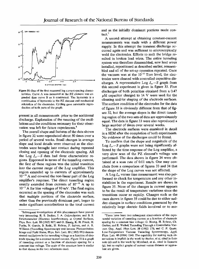
Journal of Research of the National Bureau of Standards
I 0
... . "E (J)
*-1 -2 X-3
srgrr. l). sesA (ar
Figure 3 1-One of the first measured log current-spacing charac-teristics. Curve A was measured as the PZ element was ex-panded then curve B as it contracted. The hysteresis is acombination of hysteresis in the PZ element and mechanicalrelaxation of the electrodes. Cycling gave reasonable repro-duction of both parts of the graph.
present in all measurements prior to the accidentaldischarge. Exploration of the meaning of the oscil-lations and the conditions necessary for their obser-vation was left for future experiments.'
The overall shape and features of the data shownin figure 32 were reproduced about 50 times over aperiod of several weeks. Small changes in averageslope and local details were observed as the elec-trodes were brought into contact during repeatedclosing and opening of the electrode spacing. Allthe Log 1,,-S data had three characteristic re-gions. Expressed in terms of the tunneling current,the first of these regions was the initial transitioninto the current range of the Log amplifier. Thisregion extended up to currents of approximately10'" A and covered the non-linear part of the Logamplifier's response. The direct tunneling regionusually extended from currents of 1 0 -'° A up to10-5 A for bias voltages of 10 mV. The final regionoccurred as the spacing of the electrodes was suchthat multiple portions of the electrode surface,other than the previously dominant part, began tomake significant contributions to the total current
t Subsequent investigations of this phenomenon have provedvery interesting. R. S. Becker. J. A. Golovchenko, and B. S.Swartzentruber (Electron Interferometry at Crystal Surfaces,Phys. Rev. Lett. 55 (1985) 987) and G. Binnig, K. H. Frank, H.Fuchs, N. Garcia, B. Reihl, H. Rohrer, F. Salvan, and A. R.Williams (¶4nneling Spectroscopy and Inversr PhotoemissiontImage and Field States, Phys. Rev. Lett. 55 (1985) 991) demon-strated oscillations in the tunneling voltage as a function of elec-trode spacing for aconstant tunnel current Figure 31 is a graphof tunneling current as a function of electrode spacing for aconstant bias voltage. The scale of the structure here is similarto that shown in the two references cited.
and as the initially dominant portions made con-tact.7
A second attempt at obtaining constant-currentmeasurements was made with a different powersupply. In this attempt the transient discharge oc-curred again and was sufficient to microscopicallyweld the electrodes. Efforts to melt the bridge re-sulted in broken lead wires. The entire tunnelingsystem was therefore disassembled, new lead wiresinstalled, repositioned as described earlier, reassem-bled and all of the set-up operation repeated. Oncethe vacuum was at the 10' Torr level, the elec-trodes were cleaned with controlled capacitive dis-charges. A representative Log h,,-S graph fromthis second experiment is given in figure 33. Fivedischarges of both polarities obtained from a 0.47gfd capacitor charged to 14 V were used for thecleaning and/or shaping of the electrode surfaces.The surface condition of the electrodes for the dataof figure 33 is obviously different from that of fig-ure 32, but the average slopes in the direct tunnel-ing region of the two sets of data are approximatelyequal. The data in figure 33 were also reproduced alarge number of times over several weeks.
The electrode surfaces were examined in detailin a SEM after the completion of both experiments.No evidence of the discharges could be found.
To confirm that the shape and magnitude of theLog I0,-S graphs were not being significantly af-fected by the time response of the Log amplifier, avery slow scan of the PZ element's voltage wasperformed. The data shown in figure 34 were ob-tained at a scan rate of 0.01 nm/s. One may con-clude from a comparison of figures 33 and 34 thatthe shape of the Log curves was not affected.
A Log I. versus time measurement was also per-formed to check for temperature and any other in-stabilities in the experiment. Results are shown infigure 35. None of the changes in current appearsto be the result of temperature variations since thetransitions occur so rapidly. Changes such as theones shown in figure 35 could be due to either sud-den changes in surface conditions generated by therelatively large electric fields involved or to mo-
'There have been two subsequent observations of the expo-nential variation of tunneling current as a function of electrodespacing fox a constant bias voltage: G. Birnig, H. Rohrer, ChiGerber, and E. Weibel, Tunneling Through a Controllable Vac-uum Gap, Appl. Phys Lett. 10 (1982) 178; and C. F. Quate,Low-Temperature Vacuum Tunneling Spectroscopy, Appl.Phys. Lett. 45 (1984) 1240. The capability for making such ob-servadons is implicit hi the work by Becker, et al. cited in foot-note (d) and in the work by Moreland, et al., cited in footnote(g), but no explicit graphs of current versus distance or equiva-lent are given.
209

Journal of Research of the National Bureau of Standards
lo-5
IoT
Io-
Figure 32a-Measured log current-spacing characteristics. Thesloping dashed line correspondsto a work function of approxi-mately 3.0 eV, The 100 mVcurve was measured immedi-ately following the 10 mVcurve. Horizontal placement ofthe two curves was determinedby the zeros of the PZ element'sramp generator.
W Io4
Le
U
Q04
Z 10zef
z 02=H 0-
K SIAS.+IOO mV
BIAS t lOmV
I-
I- DECREASINGELECTRODE SPACING
Similar characteristicswere measured fornegative voltagesITl
2 nal
x x-l x-2 x-3 x-4 x-5ELECTRODE SACING(nlr)
CJPPENT (AMPS)
10-5-
10-; [
1 0-7 - i~
lo-99 l
DECREASING SPACING
Figure 33-Measured log current-spacing characteristics, binsvoltage=10 mV.
t X-] x-2 x-3
ELECTIOEE SPACING (NM)
Figure 32b-Measured logvoltage= 10 mV. Curveexpanded, then curve B.
cwrrent-spacing characteristics, biasA was measured as the PZ element
tion of the electrode surfaces resulting from latticerelaxation from the strains produced by the me-chanical stress of van der Waals forces and electro-static forces. The magnitude of these mechanicalstresses is discussed in the next section.
The work functions of the electrodes may be ob-tained directly from the Log 4,,-S data given infigures 32 and 33. The slope of these curves in thedirect tunneling region may be related to the work
DECREASING SPACING
EU:TNODE SPACIw0 NaM)
Figure 34-Measured log current-spacing characteristics eN-pamded spacing scale, bias voltage= 10 mV.
210
Journal of Research of the National Bureau of Standards
| CHANGE [N CURRENT_CORRESPONDS TO ELECTRODE SPACING CHANGE OF 0.} NM
EACH TRACE TOOK APP9RXINATEL.Y 2 MINUTESLOG
L 9T JE
function with the use of eq (2-70). By taking theratio at two different spacings, one obtains
(n1, -In 12)(W W- Wost-a B)/2
where a = 10.25 (ev)" 2 (nm)-', Wj=barrierwidths at the Fermi level, and B =average barrierheight. The equation only serves to qualitativelyillustrate the method relating the slope to the WFsince B is a function of WE. The exact relation be-tween the slope of Log 14,- S data and the WF canbe obtained from the calculations of section 2.3 Thesloping dashed line in figure 32 was drawn with theuse of tables I and 2 and figure 13. Based on thediscussion of the changes in WF with adsorbed hy-drocarbons, the WF value of 3.0 eV is very reason-able. Note that this WF value was obtained withoutthe use of any assumed property of the device orthe electrode structure. The only input informationwas the piezoelectric element expansion coefficientand measured currents. This is the first time thatsuch measurements have been performed. All pre-vious measurements employed separate tunnelingdevices with thickness distributed over the valuesallowed by the fabrication process. Determinationsof the tunneling barrier thickness were also madefrom capacitance measurements and thereforewere not independent of the device characteristics.
Current-voltage measurements of the tunnelingdevice were made during the second experiment,iLe., condition B. The results for an approximate
'A recent examination of many of the topics discussed in sec-tion 2 and of the validity of measuring work functions from theslope of the In 1cv versus electrode spacing data has been per-formed by M. C. Payne and 1. C. Inkson, Measurement of WorkFunctions by Tunneling and the Effect of the Image Po tential,Surface Science 159 (1985) 485. In addition to the in 'cv versuselectrode spacing calculations given in section 2, they also use aformula derived by Simmons to compute the log of the tunnel-ing voltage as a function of the electrode spacing for a constanttunnel current density.
Figure 35-Log current vs. time fora fixed bias voltage of 10 mV.
electrode spacing of 1.2 nm are shown in figure 36.The approximate spacing of the S curve was ob-tained by determining the PZ element voltage atwhich touching occurred, assumed to be at the firstmajor drop in slope of the Log I4,-S curve, thencontracting the PZ element the desired distance.The other curves were obtained by changing theapplied PZ voltages by the amount to generate 0.1nm changes in electrode spacing, i.e., 0.2 V.
Many attempts were made to obtain a continu-ous series of 1-V graphs with electrode spacingsvarying from 2 nm to that when the electrodesmade contact. In all attempts, the state of the elec-trodes did not remain sufficiently stable for themeasurements to be performed. A series of mea-surements at two to three electrode spacings suchas shown in figure 36 was obtained four times.9
Relating the I-V data to the theoretical calcula-tions of section 2 requires an estimate of the tunnel-ing area and the absolute electrode spacing. (Thededuction of WF's from the Log 4,,-S data onlyrequired knowledge of changes in electrode spac-ing.) Ideally a consistent approach to obtainingboth the area and the absolute spacing would befirst to deduce an absolute spacing with the use ofeq (2-731) which relates the curvature of the I-V
9The author is not aware of any other published results whichshow the variation of metal-vacuum-metal tunneling 1-c curveswith small changes in electrode spacing such as is shown infigure 36. The data given by J. Moreland, S. Alexander, M.Ccx, R, Sonnenfeld, and P. K. Hansma (Squeezable ElectronTunneling Junctions, Appl. Phys. Lett. 43 (1983) 387) for silver-vacuum-silver tunneling exhibit similar properties in that theircurves have an ohmic region near zero bias with non-linear be-havior at Larger bias voltages i.e., greater than about 0.2 V. I-Vdata for structures with lead electrodes are also given whichdemonstrate behavior consistent with superconducting elec-trodes. l- V data is also given by S. A. Elrod, A. L. de Lozanne,and C. F. Quate for small bias voltages applied to a W/vacumn/NbSn structure, in the paper Low-temperature Vacuum Tun-neling Microscopy, Appl. Phys. Lett. 45 (19s4) 1240.
211
Journal of Research of the National Bureau of Standards
Figure 36a-Measured current-voltage characteristics for threeelectrode spacings. . was ap-proximately 1.2 nm. The 5,S-0,1, and 5-0.3 nm curveswere drawn manually from theA, B, and C curves of the "rawdata" of figure 36b, respec-tively. The uncertainty in S ismuch larger than that of the dif-ference between the indicatedspacings. The indicated noiselevel was a function of voltage,increasing with increasingvoltage. The source of the noisewas apparently changing sur-face condition.
-e5 -0.4 -05 -aZ -0.1
0.3 nm
/S-0.1 nm
S
VOLTAGE (VOLTS)
2xIO-
CURRENT (AMPS)
3x1O-8
Figure 36b-Measured current-voltage characteristics for threeelectrode spacings. Curves Aand B were measured with elec-trode spacings differing by 0.1nm; curve C differs in spacingby 0.2 nm from curve B.
-2xI0-8
characteristics to the barrier height and spacing.Since the barrier height can be obtained from theslope of the Log Ic-S data, the absolute spacingwould then be the only undetermined parameter.Once it is obtained, the current density calculationscould then in combination with the corresponding
53
VOLTAGE (VOLTS)
Log 4,-S data and/or the I-V data be utilizedtocalculate an average tunneling conduction area.
Let G(V)=dI(V)/dV, then carrying out thisprocedure for the S-0.1 nm curve of figure 36gives G(+0.5)/G(0)=21.42 and G(-0.5)/G(0)=12.23. The corresponding S parameters are52 =25.13 B nm2 and 52 = 15.0 B nm2 . With the Bvalues calculated from the Log Icv-S data in fig-ure 32, both values are greater than 6 nm. Based on
212
Journal of Research of the National Bureau of Standards
the procedure outlined earlier for obtaining thesedata, S should have been less than 2 nm. A possibleexplanation of this discrepancy in terms of mechan-ically generated strains is given in the next section.
Since this method for obtaining an absolute spac-ing was not reliable, an alternative means to calcu-late the area and spacing was tried. The secondapproach was to check for correspondence be-tween the area calculated from the ratio of theoret-ical current and current density calculations ofsection 2 and the area estimated from the Log4,-S data with the use of table I or eq (2-70).From the results given in table I a conduction areaof approximately 2.4 x 10i'3 mn, with a slight varia-tion with work function and electrode spacing, isobtained. If a spacing parameter S of 1.2 nm, a mea-sured current of 10- A, and a work function of 3.0eV are assumed, then one may estimate a tunnelingconduction area of approximately 5x 10¹⁶ mI2' byextrapolating the values given in table 1. This areacorresponds to a region of 20 nm radius or about1/20"' that of the radius expected for perfectspheres. Such an area is possible and could be pro-duced by microscopic projections from the spheri-cal surfaces.
However, a second possible hypothesis to ex-plain this difference between measured and pre-dicted currents is that the assumed point of contactoccurred when S was not zero. Several processesdiscussed in section 2 would produce this effect.First, the transition from equal Fermi energies toequal bulk electrostatic potentials, even though asmall effect for the almost identical electrodes ofthis equipment, could produce a change in slope ofthe Log c,-S curve that would be interpreted ascontact. Second, adsorbed or chemisorbedmolecules would produce a nonzero 5 at contact.Third, a change in slope at some value of S will beproduced by the onset of constriction resistance [71dominated current flow. For this conduction pro-cess the electrical resistance, R, between two largeconductors connected by a small conduction areaof radius, a. is given by R =p/(4ad, where p is theconductors' resistivity. Gold's resistivity is 2.3X 10⁻³ fl-m. Thus with the area resulting from thefirst hypothesis, the expected conduction resistancewould be approximately 0.3 0. The measured resis-tance at "contact" was, however, approximately104 Q. Constriction resistance for the conditions en-countered in this experiment, therefore, does notappear to be a current limiting factor.
No consistent interpretation of the data given infigures 32, 33, and 36 has been found which givesan absolute electrode spacing and a tunneling con-duction area, Future experiments will be required
to resolve the unknown relationships between thebarrier parameter S and the true physical spacing,and the difficulties of unknown conduction area.
Somewhat as a last resort the i* characteristicsof the tunneling device were explored at large elec-trode spacings. Figure 37 shows the breakdown be-havior which was typically observed for voltagesgreater than about 1.0 V, even with relatively largeelectrode spacings.
Effects of Mechanical Stress on TunnelingCharacteristics
There are two likely sources of attractive forcesbetween the tunneling electrodes which could, byproducing surface deflections, affect both the LogI vs. S and the I vs. V characteristics. These are thevan der Waals type forces between two micro-scopic bodies and the force arising from the elec-trostatic field produced by the applied bias voltage.
The van der Waals type forces between two mi-croscopic bodies spaced a distance D apart in avacuum may be calculated from a general micro-scopic theory of dispersion forces proposed by Lif-shitz [68,69]. When D is less than the smallestcharacteristic absorption wavelength of the mate-rial of the bodies, the force per unit area, SyDWibetween two planar bodies is given by
SVDW=1A/(8 r'2 D3 ) (4-1)
*co is known as the Lifshitz-van der Waals interac-tion constant. By using optical data to deduce thedielectric functions for metals and the Lifshitz the-cry, Jrupp, Schnabel, and Walter [70) computedtir for the case when both bodies were golN; tw
was found to be approximately 1.9 X 10- ' J. With
,t.r" :"Osn
1I
-3.0 -2.0 -0.0
-:1.-7
1.0
I2
2,0 3.0
5c1017
FIgure 37-Cuarent-vn.7tage characterfstic for electrode spacingof approximately 3.0 am. The breakdown behavior was typi-cal of all attempts to obtain I-V measurements for biasvoltages greater than about 1.0 V.
213

Journal of Research of the National Bureau of Standards
D expressed i nm, SVDW between gold planes invacuum is therefore given by
Substituting the sum of the stresses described byeqs (4-2 and 4-4) for q into eq (4-6) gives
SVDW Au=2X 10'/D N nm 3/m 2 (4-2)
The stress, T, produced by an electric field, E,perpendicular to a metal surface is 14]
T1 1/2cE 2, (4-3)
e=8.85X 10⁻¹² FD/m 2 . For a voltage V and elec-trode spacing D (in ni), T is therefore given by
R_W=a f [bD(r')-3+CV2 D(r'-21 dr', (4-7)
a =2(1 -p 2)/Y, b =2X I07 N nm3/m2 , andC=4.42X 10⁶N nn/V2 i 2B).
Lety =D(r')I/D then dr= 1/2 (DfR)1"2
(}9-I)- l/2 dy and,DYR2i
W(D,) =a /2 (R /D02 )1'2 f [(b/D0)y-2
T=4A42x 106 (VID) 2 N nm2/(V2 n2).
Lifshitz's theory is based on the existence of a fluc-tuating electromagnetic field in the region betweenthe two bodies and the resultant component of theMaxwell stress tensor. Thus, both types of theseforces may be viewed as being the static and dy-namic manifestation of the same force.
A complete treatment of the strains generated inthe gold electrodes by these stresses would be anextremely difficult problem. One would need to ac-count for the nonplanarity of the two electrodes interms of its effect on the van der Waals forces andthe effect of the electric field not being parallel tothe axis of the electrodes. However, since the radiiof the effective area is small compared to thesphere radius, a reasonable approximation is that allthe forces act parallel to the axis of the two spheri-cal electrodes. Further assume that the equationderived by Timoshenko and Goodier [72] for thedeflection, W(r,8), at a point (r,e) on a boundaryplane of a semi-infinite solid, produced by a stress,qfr',O'), over the area r'dr'de' holds for the sur-faces of the spherical electrodes. Timoshenko andGoodier's relation between W and q is
W(r,EO)=[(l -p')1(7rY] q(r',O') dr'de'. (4-5)
p is Poisson's ratio for the solid and Y is the elasticmodulus. Equation (4-5) is based on the assumptionthat the solid's elastic properties are isotropic.
Let Do be the minimum spacing between theelectrodes assuming no mechanical stresses werepresent. Then, for the small deviations from theaxis of the electrodes, the spacing, D, at a distancer from the axis is given by D=Do+r 2 /R; R is theradius of the electrodes. With the assumption aboutthe force directions made earlier, the maximum de-flection will occur on the axis. Here eq (4-5) gives
W=[2(l-p2)/y1f q(r') dr'.
Both parts of the integrand are standard forms. Theintegral evaluates to:
W(Do) = (a 12) (R /DJ)1`2 [6 (y - I)'/(2Duy 2)
+(3b/4Do+CV2 )Xy - I)`y
(4-9)
Let y. go to infinity, then
W(Do)r=(a/2) (RIDO2 )'12 7r/2[(3b/4Do)
+Cv1. (4-10)
Y for Gold is 8.3X 10⁹ N/m 2, p =0.33 and R = 1.5X 10⁶ nm; with these values, eq (4-10) reduces to
W(Do)r=2.JX l 7 D0D3J"
(3b4Do+ CV2 ) nm. (4-11)
For the voltages used to obtain the Log I., vs. Sdata, 10 and 100 mv, the dominant term is thatfrom the van der Waals force. If Do is I nm, thenW=3.1 rm; if D,=2 nm, then W=0.56 nm. Takinginto account the relatively gradual and controlledbehavior of most of the Log 1, vs. S data, the"avalanche" magnitudes obtained from this calcu-lation are very puzzling. The history of the elec-trodes offers a possible explanation. During theprocess to obtain the first sets of data for Log 1.,vs. 5, typified by figure 31, an abrupt transitionsuch as one would expect from the predictions ofeq (4-11) was observed. However, after the acci-dental and purposeful electrode cleaning by capac-itive discharges, the abrupt or almost step functionbehavior was no longer observed, e.g., figure 32. Ifthe capacitive discharges produced localized re-gions of smaller curvature, the magnitude of the
214
(4-4) (4-8)(p-l)-111-t-Wyl (v -1)-lilldy.
+tan-' (y _ 1)112] YIm,,.
Journal of Research of the National Bureau of Standards
deflections, from both type forces, would begreatly reduced, i.e., if R = I03 nm, then W wouldbe reduced by a factor of approximately 35 fromthat calculated from eq (4-11).
The density of electromagnetic modes for thespherical surfaces would be slightly different fromthat of the flat planes used by Lifshitz. Other mi-croscopic geometrical deviations such as plateausraised above a relatively smooth backgroundwould also affect the mode density. However, thegeometry in both cases so closely approximatesthat of two planes over the areas which would con-tribute, i.e., about 10 ,vm in radius, that the changesin the mode densities should not affect the resultgiven in eq (4-11).
The effects predicted by the voltage dependentpart support the previous proposal that the anoma-lously large curvature in the 1 vs. V data for a fixedspacing was due to mechanical stresses. The differ-ence between the theoretically calculated value ofI for a particular voltage and spacing, e.g., figures11 and 12, and that measured, e.g,, figure 36 wouldcorrespond approximately to a voltage produceddeflection of 0.08 nm for voltages of 0.35 V. Thesevalues were obtained from the s-0.3 nm curve offigure 36 as estimates of deviations from a linearI-Vcharacteristic. The change in Wbetween V=Oand V=0.35 V with Do= 1.5 nm as obtained fromeq (4-11) is 0.06 nm.IC
Conclusions
Albeit crudely, an experiment has been per-formed which demonstrates quantum mechanicaltunneling of electrons through a vacuum region ofcontinuously variable thickness. Within experimen-tal error the results indicate that an image potentialreduced barrier with the modifications suggestedby Lang and Kohn gives a close approximation tothe true barrier for metal-vacuum-metal tunneling.For the first time, the work function for the elec-trodes in a tunneling experiment has been deducedfrom experimental parameters independent of thetunneling device.
The device which was developed for this experi-ment demonstrates that vacuum tunneling experi-ments are feasible and can reliably be performed.
'"Further exploration and utilization of the effects of van derWaals forces has recently been initiated to understand the oper-ation of the scanning tunneling microscope (J. H. Coombs andJ. B. Pethica, IBM Europe Institute, STM Workshop, Oberlech,Austria, July 1-5, 1985, IBM 1 Res. and Dev. (to be published))and to enable the investigation of insulator surfaces (G. Bimnig,C. F. Quate, and Ch. Gerber, The Atomic Force Microscope,Pays. Rev. Lett. 56 930 (March 1956).
With this demonstration many new areas of re-search may be explored. A particularly direct ap-plication of the vacuum tunneling technique is thatof locating the true position of a surface to a preci-sion of 0.1 nm, 20 to 100 times greater thanpresently available techniques. Without the limita-tion to electrode materials which form oxides thatare good barriers, vacuum tunneling experimentswill be a very versatile tool for performing inelasticelectron tunneling spectroscopy.
Some contributions toward accomplishing theobjectives given in section I have therefore beenmade, but much remains to be done. The problemswhich have been discovered, e.g., strains generatedby field generated stresses and the unknown rela-tionship between physical and theoretical spacingparameters, will need resolution before furtherwork can be performed. However, the work heredoes give direction for solving the problems andonce they are solved the full potential of vacuumtunneling experiments can be realized,
Acknowledgments
The material that has been presented here is theresult of many contributions by colleagues at theNational Bureau of Standards and North TexasSate University. I particularly wish to express mythanks to: James Mackey for his consistent encour-agement and supportive friendship from the timehe agreed to act as my major professor up to thecompletion of the dissertation almost eight yearslater; Russell Young for letting me share in the ex-ploration of his new world of vacuum tunneling;Russell Young, John Simpson, and Karl Kessler forproviding the financial and management support atNBS; Fredric Scire for his creative assistance withmuch of the mechanical design and equipment con-struction; Charles Reeve for assistance with muchof the computing required for the theoretical calcu-lations; Charles Summers for his skilled machiningof the apparatus; Dwight Maxson for his designand construction of much of the early electronics,Tom Leedy for assisting with the attempt to fabri-cate a tunneling device with photolithographictechniques, Robert Hocken for sharing his knowl-edge and designs of temperature control systems,the late Henry Zoranski for the artwork depictingthe key components of the apparatus, RobertDragoset for a very helpful and thorough readingof this manuscript; and Vita Gagne and Sally Mor-ris for preparation of the final manuscript for thispublication.
The author gratefully thanks his wife, Ellen, forher many years of support during the period tocomplete this work and for her valuable assistancein preparing the original manuscript.
215

Journal of Research of the National Bureau of Standards
Appendices
Appendix 1. NUMERICAL CALCULATIONS OF TUNNELING CURRENT
The computer programs, all in FORTRAN,which were used to calculate the data for thegraphs and tables given in section 2, are containedin this appendix. The programs were executed onthe National Bureau of Standards 1lO8A Comput-ing Facility. The main programs of these computa-tions are CURDEN, to calculate the tunnelingcurrent density; CURNT, to calculate the tunnel-ing current between spherical electrodes and a pro-gram to calculate the tunneling current densityaccording to Simmins' theory.
Aside from the problems of roundoff and over-flow errors, the major difficulty which had to beovercome was long computational times. In an ear-lier version of these programs, the Newton-Raph-son method was used to find the classical turningpoints for the required energy values and a stan-dard iterative Simpson's 1/3 rule integration wasused for all integrations. With these algorithms, thecomputational time for one current density valueranged from 20 to 30 seconds, with the longertimes corresponding to larger electrode spacings.
216

Journal of Research of the National Bureau of Standards
The process of determining the turning points isdeeply nested within the chain of integrals to cal-culate the current and current density. Its computa-tional time is therefore a major component of theoverall computational time.
By changing to the indicated tanh rule for inte-grating over K(x) and using an explicit solution forthe roots of a cubic equation, the computationaltimes were cut by a factor of 10 to 15 [73]. Theiterative method of increasing the number of parti-tions until the difference between the result for nand 2n partitions was less than a specified errorwas also dropped. After determining what numberwas required for the needed accuracy, a fixed num-ber of 64 or 128 was used in all integrations. Theparticular number is specified in the programs in-volved.
With the programs as indicated, the time to com-pute one current density value was two seconds;
PROGRAM SRAMONC-'" ..............................-.. I....................CC COMPUTE APPOXIMATE VALUES OF C'SFENT DEUEIIC ACCOROTIN TO SIMIIORS THEORY. SEE THE FOUICANVhG REFERENCC HL5STE1J ELIAS AND LUNDOVIST STIG L**SJIIG F]pHENPMENAO 'H SOL[DS CH. 10 SY J. a SIMMONSC SOUJATION 11, P 14,I HAS "e CORECThED 1e READ AS F901OWSCC S2 - SI I-23<SIIS3WF.II/O3l-2ZV1,SI
C NOTE INAT FOR C - 1. VACUUM BASRFER Vl - S - SI RESALTS,C WH I15 EQOA 21 AC JO IS EON 13 IN -HE REFE V 2 CITED,
& ......... .. I--- . .......-....REAL JOJTDIMERSICKITT sIltVVS VwFI - S9'i -23./3.'WF'S+ O..-2IV'IS)VSKSNV4IS I$2UWE-{VRISIV'H IIsb2iI 12.EBS2-Ss IE-'AIOG(S7IS-S l)V1S il'S-S21llOATA WFACI5.0-1 O25G.2E14IOPENSlFILE..CfURC-:00 10 I - 3,30
iTll _ 5/.10NO 20 J - 2 11V9 -1 V20SI vVFS7 - W(SV.WF+S1
Vi - VI(S.VVAF.Sl S2)-2 VI V
JO - CIVI'EKPIA'W 'SORT(VI MWIŽ-2)JO USa - C-IV2'EXRWA'W ISRTV2)11(W-"2]UNAl - JO.) 1,)AE-99HW '300.129RV1H
20 CONTINUEW3T30ESSOOI LJTL- I **11
COG =CPMATi 2N.F4.I1IX -029 9110 CONTIFUE
STOP
the time for one current value was 15 seconds. Theresulting values, within the limitations of the physi-cal model, should be accurate to five and four sig-nificant digits, respectively, since doubling thenumber of partitions did not change the least signif-icant digit.
The fundamental data unit of the 1 108A centralprocessing unit is a 36-bit word. Average process-ing rate is about 900,000 instructions per second;0.75 microseconds for integer addition to 17.25 mi-croseconds for double precision floating-point divi-sion. Single precision floating-point numberscarried about 8 significant decimal digits (27 bits) inthe range: 2 X 10i to IX 10438. Double precisionfloating-point numbers carried about 18 significantdecimal digits (60 bits) in the range: 3 X 10 3 toS X 10+ 307
CCCCCCC
CCCCCCCCCCCCCCCCCCCCCCCCCCCCC
CCCCCCCCCC
Listing of CUROEN
CC
CCC
C
PROGRAM TUNNEL CURRENT DENSITY (CUKDER)
WRITTEN 9Y E. CLAYTON TEAGUE MAR0C 197B
SUBPROQIiAR CAILLYDT BSI1/3, FRED
THIS 1I A PROGRAM TO CALCULATE THE TU3NNELING CURRBNT AS AFUNCTION OF ELECTRODE SPACING AND AFFLIRS VOLTAGE. T11E INSUE-ATING HARRIER IS ASSUNRO TO BE VACUUM AS 1ODIIIEBO sr THE IMAGEPCTBEITIAL. THll CALCUL3I-OBS ARE BASED ON A FSEE SLECTR.a MODELFOR TGlE ELECTRODTS WITH A FREE ELECTROR PIASS IN BOTH ELECTRODESAlD IN VACUUM. A SYMMETRICAL STRUCTURE B 1n11 IEDITICALEIECTEEODES iS ASSU3ED.
TDE BASIC TUNNELIGC SQUATIONS ASSUDIN9 A WKS SOLOTIO.TO IME SCIBEOIHGIRR EQUATION ARE:(Ca.9 DUK, TUNNELING IN SOLIDS, ACACEHIC PRESS, HES YORE, 1569,PP. A9-53)CURRENT 03NHSTYIV, D, 2.( I'TElRAEO TOIN IFIIOEX3 DIhEN, V, D, I
NICK, V, TO)
WHERE:
NI(E, V, T) (4[E'I)ME)E(/['3 * LNEXOIA T)
WHERE EPOST = I + EXPL(FR-ES)/KTJ/(I +EP[CFE - EX - EV(/KTII
4(PI)MEIK/I-3 = 1.3B9910 AMPSAEV,K)
DIEB, V. DU . (1 I EXPV-(SX, V, Dl] )--
WHERE J(l:Y N, O) * IF IMIER, VN TO 33(EA, Vil0P14(1I)(2NIt10.Sj/H]['IU(Xj- EX]"3.5
THE BOTTOM OF THE CONDUCTION BAUI OF THE ' LEFT'ELECTRODE IS ASSUMED TO BE 5 . O . A VOLTAGE V IS APPLIED TOLOWER THE ELECTRON ENERGIES OF THE "RIG[N' SLECTRODE.THUS THE TOTAL POTEIITIAL ENERGY FUN:'ION FOR THE BARRIER ISGIVB/ SY:
U(X) . 0, X LESS THAN AO EQUAL TO 0D(E) . BARRIER HEIGHT - ELECTRIC POTENTIAL -IXACE POTENTIAL
lIK ' - EV I GREATER THAN Oi EQUAL TO U.
TSE SARRIER I5 THEREFORE GIVER BY:
UTCX) . FE WE - (EV/DiR -(21 0 * L3 2 ' 1.15 / ((5 P7 EPP O ' I i(O -X)
T M-1)
,Z B is In NM AmII V, FY, A3D aF ARE I VWOLTS,
217

Journal of Research of the National Bureau of Standards
C THIS REDUCES TO:CC U(X) = FE + WF - (V/D) X - 0.2867 D/ (XID-XJ).CC THUS FOR CALCULATION ONE MUST FIRST DETERMINE FOR EACH VOLTAGEC THE CLASSICAL TURNING POINTS X1(EX, V) AND X2(EX, V) FOR EACHC RELAVENT ENERGY BETWEEN 0 AND FE + WF.CC THE TUNNELING PROBABILITY IS THEN CALCULATED AS A FUNCTIONC OF ENERGY, VOLTAGE, AND BARRIER THICKNESS. AFTERC CALCULATING TilE SUPPLY FUNCTION "N" AS A FUNCTIONC OF ENERGY, VOLTAGE, AND TEMPERATURE, THE CURRENT DENSITY FLOWC IS FINALLY CALCULATED AS A FUNCTION OF THE VOLTAGEC BARRIER THICKNESS, AND TEMPERATURE.CC THE USER IS REQUESTED TO SUPPLY THE TEMPERATURE OF THEC TUNNELING DEVICE, AND THE WORK FUNCTION AND FERMI ENERGYC OF THE ELECTRODES.C
REAL NTGL1,NTGL2,NTGL3COMMON T,FE,WF,V,D,FKEXTERNAL PRODDATA NP /128/
CNP2=NP/2
CC GET TEMPERATUREC
WRITE (6,90)READ (5,80) T
CC GET FERMI ENERGYC
WRITE (6,100)READ (5,80) FE
C
Listing of DNSITY
FUNCTION DNSITY (Z)CC WRITTEN BY E. CLAYTON TEAGUE M4ARCH 1978CC SEE ANNOTATIONS IN CURRENT DENSITY PROGRAM.CC SUBPROGRAMS CALLED: RSIM13, PRODC
REAL NTGL1,NTGL2,NTGL3C
COMMON TFEWFVZ1,FKEXTERNAL PRODDATA NP /64/
CNP2=NP/2Z1=ZBLZCTT=8 . 6E-5 *TDLTA=40.*BLZCTT+VETOP=FE+WF-1. 1468/Z
CC SET MAXIMUM ENERGY BARRIER HEIGHT AS WF + DLTAC
A=ETOP-WF-DLTAC
IF (A.LT.O.) A=OB=FE-DLTAFK=1l.
CNTGL1=RSIM13(PRODABNP2)
CA=FE-DLTADIFF=ETOP-(FE+80.*BLZCTT)B=ETOP
IF (DIFF.GT.O.1) B=FE+80.'BLZCTTFK=2.
CNTGL2=RSIM13( PROD, A, BNP)
CIF (DIFF.GT.O.1) NTGL3=0.IF (DIFF.GT.O.1) GO TO 10A=ETOPB="FE+80.*BLZCTTFK=3 .
CNTGL3=RSIML3(PRODABNP2)
C10 DNSITY=NTGL1+NTGL2+NTGL3C
RETURNEND
Listing of PROD
FUNCTION PROD (EM)CC WRITTEN BY E. CLAYTON TEAGUE APRIL 1978C
C SUBPROGRAMS CALLED: RNTOP, TUNNPBC
COMMON TFE,WF,V,D,FKC
K=FKGO TO (10,20,30), K
CC NOTE THAT T IN CONSTANT OF RNTOP WAS CANCELLED BY T IN EV/KT.C10 PROD=(1.385E10 )*(V/8 .6E-5) *TUNNPB(EM)
RETURN
C20
C30C
PROD=RNTOP (EM) *TUNNPB( EM)RETURN
PROD=RNTOP(EM)((1+(D/2.2936)*(EM-FE-WF))
RETURNEND
Listing of RNTOP
FUNCTION RNTOP (EM)CC WRITTEN BY E. CLAYTON TEAGUE APRIL 1978C
DOUBLE PRECISION FERMIL,FERMIR,ALPHA,BETA,BLZCTTCOMMON T,FE,WF,V
CBLZCTT=8 .6D-S*DBLE(T)ALPHA=DEXP(DBLE(FE-EM)/BLZCTT)BETA=DEXP IDBLE(FE-EM-V)/BLZCTT)
CC AVOID ROUNDOFF ERROR IN DOUBLE PRECISION BY USING APPROXIMATIONC THAT LNUIA-A)/(1+B)( = A-B WHEN A AND B ARE MUCH LESS THAN 1.C
IF (ALPHA.LT.lD-6) GO TO 10CC AVOID OVERFLOW ERRORS BY USING APPROXIMATION THATC LN[(1+EXP(A))/)l+EXP(A+B))( = -B WHENC A IS MUCH. GREATER THAN 1.C
IF (BETA.GT.1D6) GO TO 20C
FERMIL=1 . 0DO+ALPHAFERMIR=1 . ODO+BETARNTOP=1. 385DIO*DBLE(T)*(DLOG(FERMIL)-DLOG(FERMIR))RETURN
C10 RNTOP=1. 385DlO*DBLE(T) * (ALPHA-BETA)C
RETURNC20 RNTOP=1.385DlO*DBLE(T)*DBLE(V)/BLZCTTC
RETURN; END
Listing of TUNNPB
CFUNCTION TUNNPB (EM)
C WRITTEN BY E. CLAYTON TEAGUE APRIL 1978CC SUBPROGRAMS CALLED: DCUBIC, RNIHF, RTPOTC
DOUBLE PRECISION A3,A2,AI,AO,ZlR,ZlI,Z2R,Z2I,Z3R,Z3IEXTERNAL RTPOTCOMMON TFE,WF,V,D,FK
CC CALCULATE X1(EM,V,D) AND X2(EM,V,D) TURNING POINTS.C CUBIC COEFFICIENTS CALCULATED FROM POT (IN SUBPROGRAM RTPOT).C
A3=V/DA2=-FE-WF+EM-VA1= ( FE+WF-EM )*DAO=-. 2867*DCALL DCUBIC (A3,A2,A1,AO,ZlR,ZII,Z2R,Z21,Z3R,Z3I)XlEM=Z2RX2EM=Z 3R
CC CALCULATE THE TUNNELING PROBABILITY AS A FUNCTION OF ENERGYC
IF (X1EM.LT.O.0.OR.X2EM.GT.D) GO TO 10CC CALCULATE TUNNELING INTEGRALc
Y=RNIHF(RTPOT,X1EM,X2EM, 16)CC USE MILLER AND GOOD'S FORM OF WKB APPROXIMATIONC
TUNNPB=1/( 1+EXP (Y) )C
RETURNC10 WRITE (6,20) X1EM,X2EM
TUNNPB=O .5RETURN
CC20 FORMAT (1X, 'TURNING POINTS' ,lX,F8.5,1X, 'AND' ,lX,F8.5,1X,
2 'ARE OUT OF BOUNDS --- TUNPB SET = 0.5')
END
Listing of RTPOT
FUNCTION RTPOT (XEM)CC WRITTEN BY E. CLAYTON TEAGUE APRIL 1978C
COMMON T,FE,WF,V,D,FK,EMC
POT=FE+WF-EM-(V/D)*XEM-0.2867D/(XEM*t
(D-XEM))IF (POT.LT.D.) POT=O.
218

Journal of Research of the National Bureau of Standards
CRTPOT=10.25*SQRT(POT)
CRETURNEND
Listing of RSIM13
FUNCTION RSIM13(F,A,B,N)C - - - - - - - - - - - - - - -C RSIM13 WRITTEN BY CHARLES P. REEVE, STATISTICAL ENGINEERINGC DIVISION, NATIONAL BUREAU OF STANDARDSC FOR: NUMERICAL INTEGRATION BY SIMPSON'S 1/3 RULEC SUBPROGRAMS CALLED: USER DEFINED FUNCTION FC CURRENT VERSION COMPLETED APRIL 28, 1978C - - - - - - - - - - - - - - - -
COMMON TFE,WF,V,D,FK,XN2=N/2IF(2*N2.NE.N) GO TO 5IF(A.GT.B) GO TO 4N21=N2-1H=(B-A)/NH2=2*HX=ARSIM13=F(X)X=BRSIM13=RSIM13+F(X)X=A-HDO 10 I=1,N2X=X+H2RSIM13=RSIM13+4.*F)X)
10 CONTINUEX=ADO 12 I=1,N21X=X+H2RSIM13=RSIM13+2.*F(X)
12 CONTINUERSIM13=H*RSIM13/3.RETURN
4 WRITE(6,601)601 FORMAT(1X, ***LOWER LIMIT OF INTEGRATION EXCEEDS UPPER LIMIT***'/
Listing of RSIM13
&4X, 'VALUE OF INTEGRAL SET =RSIM13=0.RETURN
5 WRITE(6,602)602 FORMAT(1X, ***THE NUMBER OF
&'VALUE OF INTEGRAL SET = O.'RSIM13=0.RETURNEND
CIF (JDIF.LT.NV) JINC=1IF (JDIF.LT.NV) GO TO 20JINC=JDI F/NV
C20 WRITE (6,170) T,WF,FE
WRITE (6,180)C
DO 50 ID=IMIN,IMAX,IINCD=ID/1000.
CDO 40 JV=JMIN,JMAX,JINC
V=JV/1000.BLZCTT=8. 6E-5
tT
DLTA=40.'BLZCTT+VCC IF (E-FE) IS LESS THAN 40KT THEN: LN(XPONT) EV/KTC
ETOP=FE+WF-1 .1468/DCC ETOP = TOP OF IMAGE POTENTIAL WITH NO BIAS VOLTAGE.CC SET MAXIMUM TUNNELING BARRIER HEIGHT AS WF + DLTACC 1ST INTEGRAL COVERS ENERGY RANGE WHERE LN(XPONT) MAY BEC APPROXIMATED BY EV/KTC
A=ETOP-WF-DLTAIF (A.LT.O.) A=OB=FE-DLTAFK=1.NTGLI=RSIM13(PROD,A,B,NP2)
CC 2ND INTEGRAL COVERS ENERGY RANGE WHERE FULL VARIATION OFC LN(XPONT) AND TUNNPB MUST BE TAKEN INTO ACCOUNT. NOTE THATC SINCE TUNNPB INCREASES AS E INCREASES UPPER LIMIT IS EXTENDEDC TO 80KTC
CC
CCC
PARTITIONS MUST BE EVEN***'/4X,
RSJM13 WAS A DUPLICATE COPY OF RSIM13
Listing of RNIHF
FUNCTION RNIHF(F,A,B,N)C - - - - - - - - - - - - - - - - - - -C RNIHF WRITTEN BY CHARLES P. REEVE, STATISTICAL ENGINEERING
C GET WORK FUNCTIONC
WRITE (6,110)READ (5,80) WF
CC GET MINIMUM ELECTRODE SPACINGC
WRITE (6,120)READ (5,80) IMIN
CC GET MAXIMUM ELECTRODE SPACINGC
WRITE (6,130)READ (5,80) IMAXIDIF=IMAX-IMIN
CC GET INCREMENTS OF ELECTRODE SPACINGC
WRITE (6,60)READ (5,80) NIES
CIF (IDIF.LT.NIES) IINC=1IF (IDIF.LT.NIES) GO TO 10IINC=IDIF/NIES
CC GET MINIMUM VOLTAGEC10 WRITE (6,140)
READ (5,80) JMINCC GET MAXIMUM VOLTAGEC
WRITE (6,150)READ (5,80) JMAXJDIF=JMAX-JM IN
CC GET INCREMENTS OF VOLTAGEC
WRITE (6,70)READ (5,80) NV
A=FE-DLTADIFF=ETOP- ( FE+80 . *BLZCTT)B=ETOPIF (DIFF.GT.O.1) B=FE+80.*BLZCTTFK=2.NTGL2=RSIM13 ( PROD,A,B,NP)
3RD INTEGRAL COVERS ENERGY RANGE IN WHICH TUNNPB IS ASSUMEDTO VARY LINEARLY WITH ENERGY, AND WHEN ETOP-FE IS LESS THAN8OKT.
IF (DIFF.GT.O.1) NTGL3=0.IF (DIFF.GT.O.1) GO TO 30A=ETOPB=FE+80 .*BLZCTTFK=3.NTGL3=RSIM13(PROD,A,B,NP2)
C30 RJ=NTGL1+NTGL2+NTGL3
WRITE (6,160) D,V,RJCC AT THE NATIONAL BUREAU OF STANDARDS COMPUTER FACILITY THE FOLLOWINGC STATEMENT WRITES INTO AN AUTOMATICALLY CREATED TEMPORARY FILE CALLEDC 7. UPON TERMINATION OF THE RUN FILE 7 MAY BE COPIED INTO THE USERSC OWN FILE FOR PERMANENT STORAGE.C
WRITE (7,160) D,V,RJC40 CONTINUE50 CONTINUE
CC
STOP
60 FORMAT ()X, 'HOW MANY INCREMENTS OF ELECTRODE SPACING?')70 FORMAT (1X,'HOW MANY INCREMENTS OF VOLTAGE?')80 FORMAT ()90 FORMAT )' ENTER TEMPERATURE IN DEGREES KELVIN (REALW)')100 FORMAT )' ENTER FERMI ENERGY IN ELECTRON VOLTS (REALW)')110 FORMAT )' ENTER WORKFUNCTION IN ELECTRON VOLTS (REALW)')120 FORMAT (' ENTER MINIMUM ELECTRODE SPACING IN PM. (INTEGER W)')130 FORMAT (' ENTER MAXIMUM ELECTRODE SPACING IN PM. (INTEGER 4)')140 FORMAT )' ENTER MINIMUM VOLTAGE IN MILLIVOLTS. (INTEGER #)')150 FORMAT )' ENTER MAXIMUM VOLTAGE IN MILLIVOLTS (1NTEGER#)')160 FORMAT (2F8.3,E12.5)170 FORMAT (1H1,/,/,8X, ' TEMPERATURE = ',lX,F5.1,' DEGREES KELVIN.' ,/,
2 8X,' WORK FUNCTION = ',lX,F4.1,' ELECTRON VOLTS. ',/,8X,3 ' FERMI ENERGY = ',1XF4.1,' ELECTRON VOLTS.',///)
180 FORMAT (8X,' COLUMN 1 = ELECTRODE SPACING IN NM.' ,/,8X,2 ' COLUMN 2 = BIAS VOLTAGE IN VOLTS.',/,8X,
3 ' COLUMN 3 = CURRENT DENSITY FLOW IN AMPERES PER SQ.M' ,////)C
END
Listing of CURNT
C PROGRAM TUNNEL CURRENT (CURNT)CC WRITTEN BY E. CLAYTON TEAGUE MARCH 1978CC SUBPROGRAMS CALLED: RSJM13, DNSITYC
COMMON T,FE,WF,VEXTERNAL DNSITYDATA NPART /16/
CC GET TEMPERATUREC
WRITE (6,80)READ (5,70) T
CC GET FERMI ENERGY
219
Journal of Research of the National Bureau of Standards
WRITE (6,90)READ (5,70) FE
CC GET WORK FUNCTIONC
WRITE (6,100)READ (5,70) WF
CC GET MINIMUM ELECTRODE SPACINGC
WRITE (6,110)READ (5,70) IMIN
CC GET MAXIMUM ELECTRODE SPACINGC
WRITE (6,120)READ (5,70) IMAXIDI F= I MAX- IM IN
CC GET INCREMENTS OF ELECTRODE SPACINGC
WRITE (6,50)READ (5,70) NIES
CIF (IDIF.Lr.NIES) IINC=1IF (IDIF.LT.NIES) GO TO 10IINC=IDIF/NIES
CC GET MINIMUM VOLTAGEC10 WRITE (6,130)
READ (5,70) JMINCC GET MAXIMUM VOLTAGEC
WRITE (6,140)READ (5,70) JMAXJDIF=JMAX-JMIN
CC GET INCREMENTS OF VOLTAGEC
WRITE (6,60)READ (5,70) NV
CIF (JDIF.LT.NV) JINC=1IF (JDIF.LT.NV) GO TO 20JINC=JDIF/tV
C20 WRITE (6,160) T,WF,FE
WRITE (6,170)C
DO 40 ID=IMIN,IMAX,IINCD=ID/1000.
CDO 30 JV=JMIN,JMAX,JINC
V=JV/1000.
CCCC
C
C
CCCCCC
C304 0C
INTEGRATE THE CURRENT DENSITY OVER SPHERICALSURFACES TO OBTAIN THE NET CURRENT FLOW.
A=DB=D+0.4CURNT=RSJM13(DNSITY,A,, HNPART)
CURNT=CURNT*3.14159265*11.5E-12
WRITE (6,150) D,V,CURNT
AT THE NATIONAL BUREAU OF STANDARDS COMPUTER FACILITY THE FOLLOWINGSTATEMENT WRITES INTO AN AUTOMATICALLY CREATED TEMPORARY FILE CALLED7. UPON TERMINATION OF THE RUN FILE 7 MAY BE COPIED INTO THE USERSOWN FILE FOR PERMANENT STORAGE.
WRITE (7,150) D,V,CURNT
CONTINUECONTINUE
STOPCC50 FORMAT (1X,'IHOW MANY TNrREMENTS OF ELECTRODE SPACING?')60 FORMAT (IX,'HOW MANY INCREMENTS OF VOLTAGE?')70 FORMAT ()80 FORMAT (' ENTER TEMPERATURE IN DEGREES KELVIN (REALI)')90 FORMAT I' ENTER FERMI ENERGY IN ELECTRON VOLTS (REALW)')100 FORMAT )' ENTER WORKFUNCTION IN ELECTRON VOLTS (REALiW)')110 FORMAT (' ENTER MINIMUM ELECTRODE SPACING IN PM. (INTEGER #)')120 FORMAT )' ENTER MAXIMUM ELECTRODE SPACING IN PM. (INTEGERt#)')130 FORMAT (' ENTER MINIMUM VOLTAGE IN MILLIVOLTS. (INTEGERW)140 FORMAT )' ENTER MAXIMUM VOLTAGE IN MILLIVOLTS (INTEGER#)')150 FORMAT (2F8.3,E12.5)160 FORMAT (1HE,/,/,8X,' TEMPERATURE = ',lX,F5.1,' DEGREES KELVIN.',/
2 OX,' WORK FUNCTION = ',1X,F4.1,' ELECTRON VOLTS. ',/,8X,3 ' FERMI ENERGY = ' ,IX,F4.1,' ELECTRON VOLTS.',////)
170 FOIR1AT (OX,' COLUMN 1 = ELECTRODE SPACING IN NM.',/,8X2 ' COLUMN 2 = BIAS VOLTAGE IN VOLTS.' ,/,8X,3 I COLUMN 3 = CURRENT FLOW IN AMPERES ',////
CEND
C DIVISION, NATIONAL BUREAU OF STANDARDSC FOR: NUMERICAL INTEGRATION USING THE TAN)! RULEC REFERENCE: HABER, SEYMOUR, THE TANII RULE FOR NUMERICALC INTEGRATION, SIAM J. NUMER. ANAL., VOL. 14, NO. 4,C SEPTEMBER 1977C SUBPROGRAMS CALLED: USER DEFINED FUNCTION FC CURRENT VERSION COMPLETED APRIL 27, 1978C - - - - - - - - - - - - - - - - -
IF(AGT.B) GO TO 41=3. 141592654/SQRtT)2.'N)-1/(2."N)
X=(B+A(/2RNIHF=F( X)DO 10 I=,Ni1I=I HY=) (B-A(/2)PTANH(HI(D=COSH OIl) *-2RNIHF=RNIHF+(FIX+Y )+F(X-Y) )/D
10 CONTINUERN IHF= ((B-A )/2 ) 'fI"RNIIIFRETURN
4 RNIIHF=OWRITE(6,600)
600 FORMAT()X,-***LOWER LIMIT OF INTEGRATION EXCEEDS UPPER LIMIT***'/&4X,'VALUE OF INTEGRAL SET = 0. IN SUBPROGRAM RNIEF')
PETURNEND
sting of DCUBIC
SUBROUTINE DCUBIC(A3,A2,AIl,AO,Z1R,Z1I,Z2R, Z2I,Z3R,Z3I)- - - - - - - - - - - - - - - - - - - - - - - - - - - - -
DCUBIC WRITTEN BY CHARLES P. REEVE, STATISTICAL ENGINEERINGDIVISION, NATIONAL BUREAU OF STANDARDS
FOR: COMPUTING TIIE ROOTS OF THE CUBIC EQUATIONA3 * X**3 + A2 * X**2 + At * X + AO = 0
WHERE THE COEFFICIENTS A3, A2, Al, AO AREDOUBLE PRECISION.THE METHOD OF SOLUTION IS TAKEN FROM PAGE 17 OF"HANDBOOK OF MATHEMATICAL STATISTICS" BYM. ABRAMOWITZ AND I.A. STEGUN, NBS-AMS-55.
SUBPROGRAMS CALLED: KJDCURRENT VERSION COMPLETED MAY 3, 1978
- - - - - - - - - - - - - - - - - - - - - - - - - - - - - - - - -
IMPLICIT DOUBLE PRECISION (A-Z)IF(DABS(A3).LE.1D-8) GO TO 4PI=3141592653589793D-15A2=A2/A3Al=A1/A3AO=AO/A3Q=A1/3-(A2/3)**2R=)A1"A2-3*AO)/6-(A
2/3)**3
T=Q* *3+R*RIF(T.LT.O.) GO TO 2T= DSQRT(T)SIC=DCBRT( R+T)S2C=DCBRT(R-T)GO TO 3
2 TCR=ODOTCI=DSQRT(-T)CR=R+TCRCI=TCIA=DATAN(CI/CR)+PI*KJD(CI,CCR)A=A/3RR=DSQRT(CR*CR+CI*CI)RR=DCBRT ( RR)SIR=RR*DCOS(A)S1I=RR*DSIN(A)CR=R-TCRCI=-TC IA=DATAN(CI/CR)(+PI*KJD(CI,CR)A=A/3RR=DSQRT(CR*CR+CI*CI)RR=DCBRT( RR)S2R=RR*DCOS (A)S2I=RR'DSIN(Al
3 UCR=-(SIR+S2R)/2-A2/3UCI=-(SI+S2I)/2VCR=-(DSQRT)3DO)/2)1(SII-S2I)VCI= ( DSQRT) 3DO)/2 )*(SlR-S2R)ZlR=SlR+S21t-A2/3ZlI=SlI+S2IZ2R=UCR+VCltZ2I=UCI+VCIZ3R=UCR-VCRZIE=UCI-VCIRETURN
4 WRITE(6,600)600 FORMAT(/1X,'NO SOLUTION -- COEFFICIENT OF X**3 IS LESS THAN 1E-8')
RETURNEND
Listing of KJD
FUNCTION KJD(T,B)C - - - - - - - - - - - - - - - -C KJD WRITTEN BY CHARLES P. REEVE, STATISTICAL ENGINEERINGC DIVISION, NATIONAL BUREAU OF STANDARDSC FOR: DETERMINING THE QUADRANT FOR THE INVERSE TANGENT FUNCTION.C THE PROPER MULTIPLE OF PI IS ADDED TO THE PRINCIPLE VALUEC OF THE INVERSE TANGENT. THE MODE IS DOUBLE PRECISIONC SUBPROGRAMS CALLED: -NONE-C CURRENT VERSION COMPLETED JUNE 8, 1976C - - - - - - - - - - - - - - - -
DOUBLE PRECISION T,BIF(T.LT.0) GO TO IIF(B.LT.0) GO TO 2KJD=ORETURN
1 IF(B.GE.O) GO TO 32 KJD=1
RETURN3 KJD=2
RETURNEND
220

Journal of Research of the National Bureau of Standards
Appendix II. STATISTICAL FLUCTUATIONS IN THE LENGTH OF A BAR
The fluctuations to be calculated here are thosearising from the thermodynamic properties of mat-ter and do not account for any additional quantumfluctuation in the length of the bar. At the tempera-tures used for this experiment, the quantum fluctua-tions would be negligible. The calculations arebased on the development given by Landau andLifshitz [74]. Starting from the argument that theprobability for a quantity x to have a value in therange x to x +dx is proportional to e '<'t whereS(x) is the entropy of the system involved and k isBoltzmann's constant, they derive the result
(A VY=-kT (o-T.(11-1)
Here (AV)2 is the mean fluctuation of the systemvolume at the temperature T.
This may be related to the properties of a solidby the bulk modulus, B, which is defined by therelation
B -V V(p) (l-2)
where V is the volume of the solid. Combining eqs(aI-I and 11-2) gives the result:
(A V)2 = kTV/B. (11-3)
If one now assumes that a bar of length, l, andcross-sectional area, A, is constrained such that all
fluctuations are manifest in length changes, thenthe result
(A1)2 =(kT/B)(/A), (11-4)
is obtained, where (Al)2 is the mean square fluctua-tion in the length of the bar.
Values for the parameters of eq (11-4) which rep-resent the gold electrode leads are
T=300 K
B = 1.0 X 10o' dynes/cm 2
1=1 cm
A = 10-2 cm2
Thus, [(AI1Y1 2=2X I1-' 5 m. Calculated values forthe fluctuations of other parts of the electrode as-sembly, i.e., the aluminum housing and the copperholders, are also close to this value for the goldelectrodes. Since this fluctuations in all the parts ofthe electrode assembly would be uncorrelated, thenet results would be the square root of the sum ofthe squares of the individual components. The re-sultant mean square fluctuations in the electrodespacing would then be approximately 4X 10-'1 m.Note that these estimates include all frequencycomponents.
221

Journal of Research of the National Bureau of Standards
Appendix III. VACUUM CONDITIONS TO ACHIEVE AND MAINTAIN A CLEANSOLID SURFACE
Let T be defined as the time in which an initiallyclean surface becomes covered with a monolayerof adsorbate when the surface is exposed to a gas ata pressure P Torr, then the purpose of this approxi-mate expression for 7' is
stant, and 1' is the gas temperature. For Nitrogen,N2 , at 300 OK,
Z = 2.873 X 1 022 P molecules/(m 2 s). (all-3)
T=2x 10⁶ /P seconds.Converting the units of P from N/m 2 to Torr gives
(III-I)
The following derivation assumes that the surfacecontains 10'9 adsorption sites/m2 and that the stick-ing coefficient for adsorption is one, i.e., every ad.sorbate molecule which strikes the surface isadsorbed.
According to the kinetic theory of gases, thenumber of molecules striking unit area per unittime, Z, is given by
Z=3.83X 1024P molecules/(m 2 s).
Time for one monolayer is density of adsorptionsites/Z, so
T= (l0 9/m 2)/Z = (2.6 x 10⁶)/P seconds. (111-5)
The general form of eq (III-I) for N adsorptionsites/unit area is
Z =NA P(27r M Rs T/-"', (11-2)
where NA is Avagadro's number, M is the molecu-lar weight of the gas, Rg is the universal gas con-
T=CVN(2rMR, T)"2 /(NA P), (111-6)
where C is a proportionality constant determinedby the adsorbate's sticking coefficient.
222
(111-4)

Journal of Research of the National Bureau of Standards
Appendix IV. AN ELECIRONIC DEVICE UTILIZING QUANTUM MECHANCALTUNNELING
The idea for this electronic device resulted fromattempts to design a metal-vacuum-metal tunnelingstructure with the use of microfabrication tech-niques commonly employed by the microelectron-ics industry. Conceptually, the device wouldcombine the properties of piezoelectric ceramicswith the high sensitivity of tunneling to changes inelectrode spacing to produce an electronic devicewith a very high transconductance.
Starting with a highly polished piezoelectric sub-strate which is polarized as a transverse expander,i.e., fields applied normal to substrate plane resultin dimensional changes in the substrate plane, thedevice would be fabricated as shown in figure 38.After applying electrodes to both faces of thepiezoelectric substrate, a thick layer of polycrys-talline metal or semiconductor, shown as the dot-ted layer, would be deposited over the anticipateddevice area. The next step would be to heavily oxi-dize the metal or semiconductor layer or by othermeans form an integral insulating layer, shown asthe lightly cross-hatched strips. Following this op-eration, the tunneling electrodes would be formedon top of the insulating layer using standard evapo-ration and photomasking technology. The finalstep in the fabrication process would be to removethe insulating layer using a preferential plasma orchemical etching process to leave a structure simi-lar to that shown in figure 38. A gap within the
range of the piezoelectric substrate would beformed by either highly precise photolithographyor by melting a narrow bridge into two parts.
Assuming that one has produced a gap betweenthe two electrodes which is shorter than the trans-verse dimensional capabilities of the piezoelectricmaterial, the device characteristics should have thefollowing qualitative properties. Let the piezoelec-trio electrodes be A and B and the tunneling elec-trodes be C and D. Then, if x, is the lateral distancebetween the bases of the tunneling electrodes andd3,, is the lateral expansion coefficient of thepiezoelectric ceramic,
dx] = (dVxlt - L)dVAB, (IV-l)
where t is the ceramic substrate's thickness, anddVAB is the change in voltage across the substrate,For a fabricated gap of 500 mu, the voltage %O, toplace the electrodes within tunneling distances foravailable piezoelectric ceramics would be approxi-mately 50 V for a 0.1 mm thickness.
Considering the device input to be the voltage
applied to the piezoelectric ceramic and the outputas the tunneling current k,,, for a fixed bias voltage,the transconductance is defined as
g = (dlc/d VAB) VCD =const. (Cv-2)
Combining eq (IV-1) and (IV-2) with the rule-of-thumb tunneling equation
CD = C 1 exp(C 2 SB ')A VCD, (IV-3)
where C,=3.16X 10i' A/m2/V, C2= 10.25 (ev)'-nmi', Sis the electrode spacing, Bthe mean barrierheight and Ais the tunneling area, gives
Figure 38-Process to fabricate tunneling devices using pho-tolEtbographic techniques g =CCB'2 eC2""'SI d 3 1 xrt-' VCD,
223
(IV-4)

Journal of Research of the National Bureau of Standards
For tunneling areas of 0lo" m', d3l=0.25 nm/V,x,=4 mm, t=O.l mm, B=l ev, S=1 nm, andVCD=O.1 V.
g =l0- A /V(=mho). (IV-5)
This value is about the maximum transconductanceobtainable with conventional electronic devices[75,76]. Increases in tunneling area to 10-`' m'would raise g to I mho.
A photograph of a device resulting from the ex-ploration of this technique for fabricating tunnelingstructures is shown in figure 39. The approach wasnot pursued any further, because at the time of theinvestigation, only limited time was available andthe preferential etching process to produce the re-quired electrode length of 2 mm was not suffi-ciently developed. Shorter lengths place demandson photomasking technology that could not beachieved, i.e., forming lines less than one microme-ter in width. However, since the time of these at-tempted fabrications, April 1976, the capabilities ofboth technologies have significantly advanced.
Figure 39-SEM photornicrograph of prototype device fabri-cated with the use of photolithographic techniques.
224

Journal of Research of the National Bureau of Standards
Appendix V. ELECTRONICS FOR THE TEMPERATURE CONTROL SYSTEM
The purpose of this appendix is to give a descrip-tion of the two-stage temperature control systemand its associated electronics in terms of the trans-fer functions of each part of the system, to derivefrom these transfer functions the, response of eachstage's control system to setpoint changes and envi-ronmental temperature changes, and finally to de-scribe the procedure employed to choose the leadand lag times of the compensation network and to"tune" the network for an acceptable response tosetpoint changes. Descriptions of both stage-con-trollers are given in terms of the block diagramshown in figure 23. The intent here is not to give adetailed analysis of the electronic circuitry, butrather to give a reasonably complete description ofthe basic properties of the control system in termsof the properties of its subunits. The transfer func-tion of each subunit will now be obtained.
The transfer function of the thermistor with re-spect to ambient changes in temperature, T, can beobtained from the equation for conservation of en-ergy
C dtz -K(T-T), (V-i)
Tz = thermistor temperature, Q = electrical powerinput, C =thermal capacity of the thermistor, andK = dissipation constant. From this equation, theeffects of input power level may also be obtained.At a steady state temperature, TSS, TZSS - TREF=-QEK. With the input power levels and dissipa-tion constants described below, Tzs-Touter=0.1mK and Tss - T inner= 1 tK. The Laplace transformof eq (V-1) gives the result
Tz(S)= [11(1 +ZS)] T(S)
+Z/[C(l +ZS)] QE(S), (V-2)
Z =K/C is the time constant of the thermistor, andS is the Laplace transform variable in the transformdomain. The thermistor transfer function with re-spect to ambient changes in temperature is there-fore
M(S) = Tz(S)/T(S) = l/(1 +ZS). (V-3)
The time constant, Z, and dissipation constant, K,for both controllers are strongly dependent on themanner in which the thermistor is mounted. Theestimates given below for K were based on themanufacturer's recommendations and the thermalconductivities of the mounting materials. Z mustaccount for the thermistor's response time and thecoupling of the thermistor to the heater and systemmass. For the thermistor's response, independent ofthis last factor, Z was approximately 1 to 10 sec-onds. Accounting for the imperfect coupling of thethermistor and heater, rough estimates for Z basedon observations of system behavior are
Zoutr-10- 2 0 s,
and
Zinner-100 -150 s.
The coupling of the thermistor and heating coils onthe inner stage was across 6 mm of the inner alu-minum enclosure.
Let Za, Zb, Z, and Zd represent the fourimpedances in a Wheatstone bridge. Then, ifZ=ZZ =Zb=Zd and Zc=Z+dZ, with dZ muchless than Z, the error signal, e, output by the bridgeis [77]
e = (E/4) (dZ/Z), (V-4)
E is the bridge excitation voltage. Thermistorshave the property that Z =Z(Tz), where Tz is thedevice temperature. Over a quite large workingrange Z(Tz) for the thermistors used in the con-troller bridges was given by Z(TZ)-Z(TREF)=a(Tz-TREF) with a =-0.04 Z(TREF)/K. Thisalong with the thermal transfer function of eq (V-3) gives
e =A (S) (T REF- Ti), (V-5)
where A(S)=k/(l+ZS), k=0.OlE V/KTo minimize the temperature difference between
the thermistor and its surroundings, the self-heatingof the thermistors by the bridge excitation voltage
225
Journal of Research of the National Bureau of Standards
must be kept to a minimum [78]. The manufactur-ers recommendation was that the self-heating beless than or equal to 0.1 of the desired control reso-lution. The dissipation constants of the two ther-mistors as mounted on the two thermal enclosureswere 90 mW/K and 42 mW/K for the outer andinner enclosures, respectively. At bridge balance,one-half of the exciting voltage will be across thethermistor. Thus, the powers which may be dissi-pated in the thermistors assuming 1 mK stability inthe outer stage and 10 jiK stability in the innerstage are 9.0 gtW and 42 nW, respectively. The rec-ommended excitation voltages are, in turn 0.85 Vand 0.13 V for the outer and inner stages respec-tively. Since any variations in these voltages wouldresult in an additional variation of the control sig-nal, stable sources are required. As a compromisebetween the recommended excitation voltage andthe need for stability, a 1.35 V mercury cell wasused for the outer-stage bridge. The inner-statebridge was driven by a stabilized oscillator with anoutput of 100 mV rms.
The circuit diagrams for both stages are shownin figures 40 and 41. The lock-in amplifier em-ployed for the sensor amplifier was an instrumentdesigned and built in-house at the National Bureauof Standards [79]. It had gain settings from 500 upto 106, time constants available from 0.5 s to 20 s,and operated at a fixed frequency of 1 kilohertz. Toa first approximation, the transfer functions of bothsensor amplifiers may, for small deviation frombridge balance, be represented by the equation
H1(S)= V1(S)/e(S)=A/(l +qS), (V-6)
A is the amplifier's dc gain or for the lock-in ampli-fier its gain when the rms value of the input is notchanging, and q is the time constant of the respec-tive amplifier. This transfer function for the lock-inamplifier represents the relationship between thedc output voltage and the rms value of the input acsignal with the selected phase. For the lock-in am-plifier, q is simply the time constant setting of theamplifier's low pass filter. Equation (V-6) assumesthe lock-in filter is equivalent to one RC stage. Forthe sensor amplifier of the outer-stage-controller, qwas set by the 0.004 ptfd capacitor at 4X 10² ssince this was the approximate value expected fromthe 12 dB/octave gain characteristic and antici-pated gain setting.
For both stages, the bridge-sensor amplifier com-bination was configured to obtain the required neg-ative feedback. With the outer stage controller, thisonly amounted to choosing the correct polarity ofthe bridge excitation voltage. With the lock-in am-plifier, this was accomplished by choosing the ap-propriate phase to detect.
A brief note about the particular bridge circuitused for the outer sensor amplifier. This circuit al-lows the use of a single-ended, chopper-stabilizedamplifier and its attendant low drift. Another ad-vantage of the circuit is that the gain is not depen-dent on the absolute value of the bridge resistorsand can be simply adjusted by changing the ratio ofthe 10 nfl and 10012 resistors.
GALS I ~~~~~~~~~~~~~~suppty
100
DS
Figure 40-Schematic of electron-ics for outer temperature con-trol stage.
NOTE: ALL RESISTANCES IN OHMSALL CAPACITANCES IN MICROFARADS
'TEMPERATURE COEFF. = 1 PPM/°C5 PPM/YR
226

Journal of Research of the National Bureau of Standards
SUPPLY
SEVEN DIGIT RATIO TRANSFORMERSINGEIV-OERTScY O u1IR
1000DUMB1
Figure 41-Schematic of electron-ics for inner temperature con-trol stage.
ALL RESISTANCES IN DUN0S
ALL CAPACITANCES IN MICROFARADSC' P 8UTN6R 8P3yN 8 T INLEADTEMP. COEFF, = 1 PPM/C TEMP. STABILITY - 5 PPM/YR
The transfer function of the compensation net- of the differentiation time constant and this chan-work shown in figure 42 is given by [80] nel's gain. The time constant, a, was 0.2 s for the
H2 (S)= V2/VI =P+ DS [/5 outer-stage controller and 2.0 s for the inner-stage(1 +aS)(I +1bS) controller; b was 0.5 D for the outer-stage and 0.05
(V-7) D for the inner-stage. The open loop transfer func-tion of the operational amplifiers used in the com-
where P is the proportional gain setting, I is the pensation network is to first orderproduct of the integration channel's gain and theinverse of the integration time and D is the product M(S)=2X 10⁻⁵/(1+6X10- 3 S). (V-8)
INPUT
OUTER STAGE: C2- 0.2INNER SlAGE, '2- 2.0
Figure 42-Schematic of compen-sation network used for bothtemperature control stages.
227

Journal of Research of the National Bureau of Standards
Since this pole and the pole at S = 100 in the pro-portional channel are so much higher frequencypoles than all the other poles of the controllers,their effects, which are minor, will not be includedin the following discussion.
The response properties of the power amplifierfor both control stages can be understood by not-ing that a fundamental property of an operationalamplifier is to maintain the summing point, i.e., theinverting input, at a "virtual ground" condition[80). The implication of this property for the poweramplifier portion of the controllers is that all cur-rent flow to the inverting input of the operationalamplifier which drives the MOSFET power tran-sistor, a VMP-12 or 22, must also flow through the10 Ka feedback resistor, RF,, connected to thedevice's source terminal. (This, of course, neglectsthe small amount flowing through the 100 Kf re-sistor to the operational amplifier output.) Thiscondition can be used to relate the voltage appliedto the heater, V3, and the equivalent voltage out-put from the compensation network with an equiv-alent input resistance, Ri, of 100 Kfls. Thus, withthese definitions; V2=1 R1, where I is the summedcurrent. The voltage at the source terminal willthen be maintained at; VFB=IRFE. But, YFB=(V3/RH)RB, from a simple application of Ohm's law. So
necting leads, and the epoxy supports used to ther-mally isolate the outer stage from the granitevibration isolation table. For the inner stage, thesepaths include the electrical connecting leads andthe ceramic supports. By analogy with electricalcircuit terminology, R is given by R =(RA-TE)lQc, where Ts= temperature of stage, Ts= temper-ature of the stage's environment and Qc=powerloss due to conduction.
Radiation transfer of energy is a major factorwhich must be considered in the design of the innercontrol stage. Zemansky [81] shows that the rate ofenergy transfer QR, between a body with emissiv-ity, e, and temperature, T, and a surrounding sys-tem at temperature, TF, is given by
QR=Aieo-(T'-TE). (V-lI)
Here A is the surface area of the enclosed body anda- is the Stefan-Boltzmann constant.
With the use of this lumped parameter model,the thermal behavior of each stage can be de-scribed by the equation for the conservation of en-ergy
Q =QIN-Qc- QR (V-12)
orV3=(RFBdR-j(RH1RB) V2. (V-9)
Here RH is the heater resistance and R, is the biasresistance between common and the device sourceterminal.
The transfer function of the power amplifier isdetermined by the do gain obtained from eq (V-9)and the response of the operational amplifier in thefeedback loop. The corner frequency of the MOSdevice is greater than 100 MHz. Thus, the overalltransfer function of the power amplifier would be
H,(S)= V3/V2=Ap/l +Ps),
CdT = V2/r-(T-T,)/R -A cor(T4-Tp4),
(V-13)
where C is the heat capacity of each stage, V is thevoltage applied to heater coils of resistance r, andthe other symbols are as defined previously. If eq(V-13) is linearized by expanding 1 and V abouttheir operating point values, TREF and V0, at whichdT/dt =0, the following equation holds for smalldeviations about these values
(V-lo)
with AP= (RFU/Ri)(1R~j/Rn) and p=6X10 3 ' s. Asindicated for the compensation network, the effectsof this high frequency pole are not accounted for inthe following discussion.
To obtain a model of the thermal response of theheaters and their respective masses, a simplelumped parameter model of the heat conductionand radiation was utilized. Referring back to figure22, let R represent the thermal resistance of all con-duction paths between each stage's componentsand its environment. For the outer stage, thesepaths include the polyurethane foam, the stainlesssteel ports to the vacuum pumps, the electrical con-
dT 1 2Vodt kCC RC R'C
where R'= I/R +4A EOrTREF'. Lett,=rC, then the Laplace transformgives the result
T(S)= G1(S)V(S)+G2 (S)TE(S)
(V-14)
t1t=R'C andof eq (V-14)
(V-15)
where G1(S)=2Vctr1/Q6 (l+trS)) and G2(S)= l(1+tS).
The transfer function of the cascaded sensor am-plifier compensation network and power amplifier
228

Journal of Research of the National Bureau of Standards
is given by the product of their individual transferfunctions [82]. Therefore, let
H(s)= V3/e =H,(S)XXH2(S)X1 3(S). (V-16)
The controllers' feedback responses are then deter-mined by the equations
outer stage:S3+ 15S3+[51 + 10/D],S + 10 I/D =0,
and inner stage:SI+ IS2+ [201+ l0/D]2S + 10 I/D =0.
(V-22)
(V-23)
For eqs (V-22 and V-23), the roots are approxi-mately [83]:
outer stage:51_- 15, Sa, 53-2)[]1ISF -[ II'/2V= V3=H(S)3
T=G1 (S)V+G 2(S)Tc. (V-17)
The transform variable is not indicated on thedependent variables. Solving this set of equationsfor T gives
T=[G2(S)TE+A(S)G1(S)H(S)TREF] F(S)
F(S)= [1 +A (S)G 1(S)H(S)]-l. (V-18)
The following discussion is presented in terms ofchanges in TREEF While the transient response of thesystem is different for changes in TREE and Ts, thestability conditions are the same for both systemchanges. Calculations were only made in terms ofchanges in TREF since step changes in TREF wereanticipated.
Let K(S)= T(S)/TREF(S), then
K(S)= GI(S)H(S)A (S)F(S). (V-19)
K(S) is the overall transfer function describing theresponse of the closed loop system to changes inthe setpoint, TREE. Substitution of the variousparameter and function definitions yields the result
G0(S)H(S)A (5)
g(S +S1)(S +S2)(S +S)S(+ tSXI+aS)(I +bS)(I +ZS)(I +±S),
(V-20)
where g =2kAAV 1t//t,.The zeros S,, S, and S, are the roots of the equa-
tion
S3+[1/p + I/b + I/a +D/(abP)]S'
+ [/bP +1/aP +I/ab]S +J/abP =0. (V-21)
This equation reduces to the following equationsfor the two stages;
and inner stage:51=- 11, SI, 53-_-(25,)`[ ],+5i` []2'
Parameters of the outer-stage controller were
heat capacity= C = 1.42 X 10+ J/0Cheater resistance = r = 60 Qthermal resistance=R =0.8 'C/Wsteady state voltage= VO=20 Vbridge constant=k=0.0l V/0 Cstage time constant=RC =t,=1.lX> 04spower amplifier gain=A,=6
The poles, other than the high frequency ones notaccounted for in eq (V-20), were a =0.25s,b=0.5Ds, Z=10-20s, and q=4Xlo- 2s.
Parameters of the inner-stage controller were
heat capacity=C=2.9x0O3 J/Cheater resistance =r= =.05 X I03 IIthermal resistance=R =8 0 C/Wsteady state voltage= V,= 10 Vbridge constant = k = I X 10- 3 V/=Cstage time constant=RC =2.3X 10⁴spower amplifier gain =A,= 3
The poles were located at a =2.0s, b =0.05Ds,ZE00iO-150s, and q=0.5-2s. The thermal resis-tance R of this stage represents the parallel resis-tance of conduction and radiation.
The poles and zeros of K(S) in the S-plane com-pletely determine the stability of the temperature-control stages and their transient responses tochanges in setpoint temperature and environmentaltemperature [82]. Some guidelines for the design ofa feedback system which are usually scatteredthroughout most texts on control systems are
A. The system will be unstable if K(S) containsany poles in the right half-plane.
B. The system's transient response is increas-ingly oscillatory as the poles of K(S) movetoward the imaginary axis.
229

Journal of Research of the National Bureau of Standards
C. The system's speed of response is propor- An attempt was made to use these guidelines intional to the distance of the dominant poles adjusting the lead and lag times of the compensa-from the S-plane origin. tion networks. The procedure for adjustment was
D. Introduction of negative real zeros in K(S) in to set l and D to zero and P = I. The overall gain ofgeneral increases system stability. the feedback loop was then increased by increasing
E. The relative weighting, Rk, of the k~' mode of A, the sensor amnplifer gain, until the stage-con-a system, i.e., a pole or a complex pair of troller broke into oscillation. D and I were thenpoles, is determined by increased to the values calculated below; D to
eliminate the instability by introducing zeros nearthe origin and I to eliminate or minimize any offset
1Rk = I (VI24) by introducing a pole at the origin. The effects ofthese changes can be visualized in terms of a root-
PI I PI i-PfI locus diagram. This type of diagram is a graph ofi--k the paths traced by the poles of K(S) as g of eq
where ni, i= 1, mn are the zeros of K(S) and (V-20) is varied from zero to infinity. A root-locusPi, 1 = 1, n, are the poles of K(S). Thus, plac- diagram, constructed with the aid of the root-locusing zeros near troublesome or oscillatory properties described by Fortmann and Uitz 84]poles minimizes their effect. and Kuo [85], for K(S) of the outer-stage con-
F. The response of a feedback system (as in fig. troller is sketched in figure 43. Only the dominant23) to a constant reference input has a zero poles and zeros are drawn since the effects of thesteady-state error if and only if the open loop other ones are principally to change the angles oftransfer function G,(S)H(S)A(S) has at least the asymptotes of the root-loci.one pole at S =0. For zero steady-state error An examination of the diagram in figure 43 willwith reference inputs of the form, a tn, the show that before compensation, the two dominantrequirement is that GQ(S)H(S)A (S) have a poles are the ones due to the thermal lag of thepole at S= Owith multiplicity m greater than stage mass and to the time constant of transferringn, energy from the heater to the thermistor. These are
G. For disturbance inputs, a similar property labelled l1t/ and l/Z, respectively, in the diagram.holds. Here the pole at S=0 must be in the The compensation network introduces three zeroscontroller transfer function H(S). Therefore, and three new poles. The zeros tend to straightena controller with a pole at S = 0 insures that a the root-locus branch that causes instability so thatzero steady-state error may be achieved in the same gain may be used with no oscillations. Anboth cases. equal margin of stability without compensation
AFETER
1/(.5 C)
O ZERO
K POLE
I OPERATING POINT(ESTIMATED)
BEFORE /
C*I4YENSATION
Figure 43-Root-locus diagram fortemperature control system.
230
I

Journal of Research of the National Bureau of Standards
would have required significantly reduced loopgain and, thus, less attenuation of environmentaldisturbances.
D and I were initially chosen to bring the zeros,S2 and S3, to be adjacent to the pole at 1/Z to ap-proximately cancel its effect. From the roots givenfor eqs (V-22 and V-23), this condition requiresthat for the outer stage
TO [51 + IO/D] =0.1I
and for the inner stage
1 j E201I+10D] =0.01
Initial setting for D and I were
for outer stage:
I0
3
zz
3:
0
0.
zIr
00.
TIME IHOUFISI
I=0.1 S-', D=3s
and for inner stage:
1=0.01 St',D=50s.
After some "tweaking" of 1, D, and P to getmaximum gain without oscillations, the responsesto setpoint changes shown in figures 44 and 45were obtained. These responses are certainly notoptimum, but are acceptable. The sensor amplifiergains and compensation network settings to obtainthese responses were: outer stage -A = 5000 V/V,1=0.013 stl, D=4 s, P=l, and inner stage -
A=5X10⁵ V/V, 1=0.015 s',D=200 s,P=0.75.With these sensor amplifier gains, the closed
loop gain, including the bridge and thermistor re-sponse, were
outer stage: ACL =A A,, k = 3,000 V/'C
inner stage: ACL=A AP k = 15,000 VtC.
Figure 44-Respotue of outer temperature control stage to set-point change.
Figure 45-Respomse of inner tem-perature control stage to set-point change.
TIME IMINUTES)
231
4 r

Journal of Research of the National Bureau of Standards
References
[I] The example given is similar to an analogy given by Lan-genberg, UN. The 1973 Nobel Prize for Physics, Science182 701 (1973).
[2] Schrddinger, P., Quantization as a problem of proper val-ues, Part I. Annalen der Physik. 79 361 (1926). Part 11, 79489 (1926). Part III, 80 437 (1926). Part IV, 81 109 (1926).
[3] Oppenheimer, J.R., Three notes on the quantum theory ofaperiodic effects. Phys. Rev. 31 66 (1928).
14] Fowler, R.H., and L. Nordheim, Electron emission in in-tense electric fields, Proc. Roy, Soc. (London) 119 173(1928).
[51 Gamow, G., Zur quanten theorie des atonstnerac Z.Phys. 51204 (1928).
[6] Frenkel, J., On the electrical resistance of contacts be-tween solid conductors, Phys. Rev. 36 1604 (1930).
[73 Holm, R., Electric contacts. New York: Springer-Verlag(1967).
[8] Giaever, I., Energy gap in superconductors measured byelectron tunneling, Phys. Rev, Lett. 5 t47, 464 (1960); andElectron tunneling and superconductivity, Science 1831253 (1974) Nobel Prize Lecture.
(91 Esaki, L., Long journey into tunneling, Science 183 1149(1974) Nobel Prize Lecture; and Phys. Rev. 109 603(1958).
[10] Josephson, B.D., Possible new effects in superconductivetunneling, Phys. Lett. 1251 (1962); and discovery of tun-neling supercurrents, Science 184 527 (1974) Nobel PrizeLecture.
[I I] Lambe, J., and R.C. Jaklevic, Molecular vibration spectraby inelastic electron tunneling, Phys. Rev. 165 821 (1968).
[12 Young, R.D.; J. Ward, and F, Scire, Observation ofmetal-vacuum-metal tunneling, Field emission, and thetransition regmn, Phys. Rev. Lett. 21 922 (1971); andYoung, R., J. Ward, and F. Scire, The topografiner: Aninstrument for measuring surface rmicrotopography, Rev,Sci. Instrum. 43 999 (1972).
[13] Thompson, W.A., and S.F. Hanrahan, Thermal drive ap-paratus for direct vacuum tunneling experiments, Rev.Sci. Instrum. 47 1303 (1976).
[143 Bursteil, E., and S. Lundqvist, Tunneling phenomena insolids. New York: Plenum Press (1969).
[15] Duke, C.B., Tunneling in solids, New York: AcademicPress (1969).
[16] Simmons, J.G., Generalized formula for the electric tun-nel effect between similar electrodes separated by a thininsulating film. J. Appl. Phys, 34 1793 (1963).
[17] Harrison, W.A., Tunneling from an independent-particlepoint of view. Phys. Rev. 123 85 (1961).
[18] Stratton, R., Volt-current characteristics for tunnelingthrough insulating films. J. Phys. Chem. Solids 23 1177(1962).
[191 Brinkman, W.F.; R.C. Dynes, and J.M. Rowell, Tunnel-ing conductance of asymmetrical barriers, J. Appl. Phys.41 1915 (1970).
(20] Applebaum, J.A., and W.V Brinkman, Theory of many-body effects in tunneling, Phys. Rev. 186 464 (1969).
(21] Caroli, C.; R. Cambescot. D. Lederer-Rozenblatt, P.Nozieres, and D. Saint-James, Comment on a recent the-ory of tunneling without the transfer Hamiltonian formal-ism, Phys. Rev, B 12 3977 (1975), and referencescontained therein.
[221 Feuchtwang, T.E., Theory of tunneling without transfer-Hamitionian, Phys. Rev. B 12 3979 (1975), and referencescontained therein.
(231 Kurtin, S.L.; T.C. McGill, and C.A. Mead, Direct intere-lectrode tunneling in GaSe, Phys. Rev. B 3 3368 (1971).
[24] Duke, C.B.; Reference 15, pp. 60-65.[253 Lang, N.D., and W. Kohn, Theory of metal surfaces:
charge density and surface energy, Phys. Rev. B 1 4555(1970).
[26] Lang, N.D., and W. Kohn, Theory of metal surfaces:work function, Phys. Rev. B 3 1215 (1971).
(27] Lang, N.D., and W. ICohn, Theory of metal surfaces: in-duced surface charge and image potential. Phys. Rev, B 73541 (1973).
[28] Kohn, W., and L.J. Sham, Self-consistent equations in-cluding exchange and correlation effects. Phys. Rev. 140Al 133 (1965); and P. Hohenberg and W. Kohn, Phys.Rev. 136 B864 (1964). See also Lang, N.D., Density-func-tional formalism and the electronic structure of metal sur-faces, Solid State Physics 28 225 (1973).
[293 Hedin, L., and B. Lundqvist, Explicit local exchange-cor-relation potentials, J. Phys. C 4 2064 (1971).
[301 Slater, J.C., The self-consistent Field for molecules andsolids, New York: McGraw-Hill Book Co. (1974) Chapter2.
[31] Moruzzi, V.L, J.F. Janak and A.R. Williams, Calculatedelectronic properties of metals. New York: PergamonPress (1578) p, 9.
[32] Eastman, D.E., Photoelectric work functions of transi-tion, rare-earth, and noble metals, Phys. Rev. B 21(1970);and GA. Haas and R.E. Thomas, Thermionic emissionand work function, in Measurement of physical proper-ties, E. Passaglia, ed., Vol. VI of Techniques of metalresearch, R.P. Bunshah, ed. New York: Interscience Pub-lishers (1972).
133] Bardeen, J., Theory of the work function, Phys. Rev. 49653 (1936).
[343 Applebaum, J. A., Electronic structure of solid surfaces, inSurface physics of materials, J.D. Blakely, ed., New York:Academic Press (1975); and Applebaum, J.A., and D.R.Hamann, Electronic structure of solid surfaces, Rev. ofMod. Phys. 48 479 (1976).
[35] Kittel, C., Elementary statistical physics. New York: JohnWiley (1958) pp. 25-31.
[363 Spenke, E., Electronic semiconductors. New York: Mc-Graw-Hill Book Co. (1958) Chapter 10.
(37] Bennett, A.J., and C.B. Duke, Self-consistent model ofbimetallic interfaces, Phys. Rev. 160 541 (1967).
[38] Simmons, J.G., Image force in metal-oxide-metal tunneljunctions, in Reference 14.
[39] Duke, C-B., Reference 15, p. 6 and p. 207.[40] Landau, L.D., and E.M. Lifsiitz, Quantum mechanics:
non-relativistic theory, 3rd ed, Oxford, England: Perga-mon Press (1977) pp. 55-60.
[413 Blatt, J.M., and V.F. Weisskopf, Theoretical nuclearphysics. New York: John Wiley and Sons (1952) pp. 528-529.
(421 Merzbacher, E., Quantum mechanics, 2nd Edition, NewYork: John Wiley and Sons (1970) pp. 116-126.
[43] Bohm, D., Quantum theory. New York: Prentice-Hall,Inc. (1951) pp. 271-277.
[44] Duke, C.d., Reference 15, p. 59.[45] Politzer, B.A., Comparison of a numerical method and
the WKB approximation in the determination of transmis-sion coefficients for thin insulating films, J. Appl. Phys. 37279 (1966).
[46] Simmons, J.G., Generalized formula for the electric tun-nel effect between similar electrodes separated by a thininsulating film, 1. Appl. Phys. 341793 (1963); and J. Appl.
232
Journal of Research of the National Bureau of Standards
Phys. 35 2655 (1964). The forms of the image potentialgiven here must be corrected according to the paper bySimmons in Reference 14.
[47] Simmons, J.G., J. Appl. Phys. 34 238 (1963).[48] Knauss, H.P., and R.A. Breslow, Current-voltage charac-
teristic of tunnel junctions, Proc. IRE 50 1834 (1962).[49] Rowell, J.M., Tunneling anomalies-experiment, in Ref-
erence 3.[50] Murphy, E.L., and R.H Good Jr., Thermionic emission,
field emission, and the transition region, Phys. Rev. 1021464 (1956).
[51] Young, R.D., Theoretical total-energy distribution offield-emitted electrons, Phys. Rev. 113 110 (1959).
[52] Miller, S.C. Jr., and R.M. Good Jr., A WKB-type approx-imation to the Schrddinger equation, Phys. Rev. 91 174(1953).
[53] Hunter, J. L., Acoustics. Englewood Cliffs, NJ: Prentice-Hall, Inc. (1962), Chapter 8.
[54] Rhodin, T.N., and D.L. Adams, Adsorption of gases onsolids, Chapter 5 in Treatise on solid state chemistry: sur-faces, N.B. Hannay, ed. New York: Plenum Press (1976).
[551 Chesters, M.A., and G.A. Somorjai, The chemisorption ofoxygen, water, and selected hydrocarbons on the (11)and stepped gold surfaces, Surf. Sci. 52 21 (1975).
[561 Trapnell, B.M.W., The activities of evaporated metalfims in gas chemisorption, Proc. Roy. Soc. A218 566(1953).
[57] Gland, J.L., and G.A. Somorjai, Low-energy-electron-diffraction and work function studies of adsorbed organicmonolayers on the (100) and (1:1) crystal face of plat-inum. Advances in Colloid and Interface Science 5 205(1976).
[58] Hocken, R., Physicist at National Bureau of Standards,private communication.
[59] Cutkosky, R., and D.F. Field, Standard cell enclosurewith 20 pK stability, IEEE Trans. Instrum. Meas. IM-23295 (1974).
[60] Emerson and Cuming, Inc.; Canton, MA 02021; Stycast2850KT with catalyst 24LV for cylindrical walls, catalyst9 for top and bottom surfaces.
[61] The particular ceramic used was PZT-8, manufactured bythe Vernitron Corporation; Piezoelectric Division; 232Forbes Road; Bedford, OH 44146. A general descriptionof this class of ceramics is given in Piezoelectric Ceram-ics, by B. Jaffe, W.R. Cook and H. Jaffe, New York: Aca-demic Press (1971).
[62] Emerson and Cuming, Inc.; Canton, MA 02021; Ec-cohond Solder V-91.
[63] The insulating film used was "Kapton" manufactured byE.l. duPont deNemours and Company, Inc.; PlasticsProducts and Resins Department; Industrial Films Divi-sion; Wilmington, DE 19898. Kapton is a mechanicallystrong, transparent amber-colored film which has a verylow outgassing rate and a dielectric strength of 2.75 X 10'V/mm. The manufacturer specifies that no outgassingwas revealed by weight loss at 200 'C and 3 X 10- Torrpressures. This behavior was confirmed before use in thisexperiment by observing that a piece .25mX 25mX25
micrometer thick could quickly be pumped down to apressure of 10<5 Torr with a 50 I/s ion pump system.
[641 Model 341A D.C Voltage Calibrator manufactured byJohn Fluke Mfg. Co., Inc.; P.O. Box 43210: MountlakeTerrace, WA 98043.
[65] Scire, F.R, and E.C. Teague, Piezo-driven 50 micrometerrange stage with sub-nanometer resolution, Rev. Sci. In-strum. 49 1735 (1978).
[663 Morse, P.M., and K.V. Ingaid, Theoretical aconstics.New York: McGraw-Hill Book Co. (1968) Chapter 5.
[673 Crandall, S.H., The role of damping in vibrational theory,J. of Sound Vibr. 113 (1970).
[68] Lifshitz, E.M., The theory of molecular attractive forcesbetween solids, Soviet Physics, J, of Experimental andTheoretical Physics 2 73 (1956).
[69] Israelachvili, J.N., and D. Tabor, Van der Wanls forces:theory and experiment in progress in surface and mem-brane science, Volume 7, J.F. Danielli, M.D. Rosenberg,and D.A. Cadenhead, eds, New York: Academic Press(1973).
(70] Krupp, H.; W. Schnabel and G. Walter, Journal of Col-loid and Interface Science 39 421 (19X2).
[71] Panofsky, W.K.H., and M. Phillips, Classical electricityand magnetism. Reading, MA: Addison-Wesley Publish-ing Co. (1962) pp. 103-107.
[72] Timoshenko, S., and J.N. Goodier, Theory of elasticity.New York: McGraw-Hill Book Co. (1951) pp. 362-372.
[73] The author is indebted to C.P. Reeve, National Bureau ofStandards, for suggesting and assisting with thesechanges.
[74] Landau, L.D., and E.M. Lifshitz, Statistical Physics.Reading, MA: Addison-Wesley Publishing Co. (1969) pp.348-352.
[75] Grove, A.S., Physics and technology of semiconductordevices. New York: John Wiley and Sons, Inc. (1967) p.253.
[76] Boylestad, R., and L. Nashelsky, Electronic devices andcircuit theory. 2nd ed. Englewood Cliffs, NJ. Prentice-Hall, Inc. (1978).
[77] Terman and Pettit. Electronic measurements. New York:McGraw-Hill Book Company (1952) pp. 74-83.
[78] Thermistor Manual, Bulletin EMC-6, Fenwal Electronics(1974),
[79] The amplifier was designed by Mark Horowitz, NationalBureau of Standards.
[80] Wait, J.V.; L.P. Huelsman, and G.A. Korn, Introductionto operational amplifier theory and applications. NewYork: McGraw-Hill Book Company (1975) pp. 1-55.
(81] Zemansky, M.W., Heat and thermodynamics. New York:McGraw-Hill Book Company (1957) p. 106.
[82] Fortmann, T.E,, and K.L. Hitz, An introduction to linearcontrol systems. New York: Marcel Dekker, Inc. (1977)pp. 159-386.
(831 Uspensky, J.V., Theory of equations. New York: Mc-Graw-Hill Book Company (1948) pp. 82-94.
[84] Reference 82, pp. 300-307.[85] Kuo, B.C., Automatic control systems. Englewood Cliffs,
NJ: Prentice-Hall, Inc. (1962) pp. 1-170 and 246-300.
233

Journal of Research of the National Bureau of Standards
Conference Reports
CONFERENCEON PRECISIONELECTR OMAGNE TICMEASUREMENTSThe 15th Conference on Precision Electromag-netic Measurements, CPEM '86, was held fromJune 23 to June 27, 1986, at the National Bureau ofStandards' Gaithersburg, MD, location. This con-ference, permanently cosponsored by the NBS, theIEEE Instrumentation and Measurement Society,and the International Union of Radio Scientists(URSI), is held every two years, alternately on theNorth American continent and elsewhere in theworld. It provides an international forum for engi-neers and scientists responsible for the develop-ment of standards, instrumentation, and techniquesfor the measurement of electromagnetic quantitiesacross the entire frequency spectrum at the highestpossible levels of accuracy.
The keynote address was delivered by NormanF. Ramsey, Higgins Professor of Physics, HarvardUniversity. In his talk, entitled "Quantum Mechan-ics and Precision Measurements," Ramsey re-viewed the tremendous improvements in theaccuracies of standards, progress in the understand-ing of basic physical processes, and increases inmeasurement compatibility made possible by quan-tum theory. Quantum mechanics has made possiblestandards based directly on underlying atomicparameters and fundamental physical constants.The adaptation of these standards in the place ofartifact standards has led to an increase in accuracyof 4 orders of magnitude over the past 50 years.
Jan K. Harvey of the National MeasurementLaboratory, CSIRO, Australia, was presented theIEEE Morris E. Leeds Award for his contributionsto the use of superconducting phenomena for pre-
cision measurements. Mr. Harvey spoke on "TheDevelopment of the Australian Voltage Standard"following his acceptance of the award. The awardwas presented by Bruno 0. Weinschel, president ofthe IEEE, who also spoke briefly, following Mr.Harvey's talk, on the responsibilities of govern-ments and national standards laboratories vis-a-visthe balance between science and engineering workin the measurements field.
The opening plenary session ended with brieftalks by Per 0. Lundboin, Stefan Hahn, and PierreGiacomo, addressing the assembled conferees onbehalf of the International Electrotechnical Com-mission (IEC), the International Union of RadioScientists ("RSI), and the International Bureau ofWeights and Measures (BIPM), respectively.
One of the highlights of the conference came onTuesday morning when the 1985 Nobel PhysicsLaureate, Klaus von Klitzing, spoke on "HistoricalAspects of the Quantum Hall Effect" in a plenarysession. His review of the work that led to his dis-covery of the quantized Hall effect in 1980 pro-vided an excellent coverage of experimental andtheoretical work in the field of two-dimensionalelectron gases. His talk was not without-vonKlitzing showed also how his career and momen-tons discovery had been forecast by astrologicalmeans.
The current high level of interest and researchon the quantized Hall effect led to two strong ses-sions on activities by the national laboratories todevelop resistance standards based thereon. Thesesessions were kicked off by an invited talk byToichiro Kinoshita, noted theorist from theNewman Laboratory for Nuclear Studies, CornellUniversity, who spoke on the anomalous magneticmoment of the electron and the QED-computeddetermination of the fine structure constant.Eleven contributed papers described quantizedHall effect work in Australia, France, U.K., WestGermany, Japan, Canada, Switzerland, BIPM, andthe USA.
235

Journal of Research of the National Bureau of Standards
New and exciting work was presented in fivesessions on laser frequency stabilization and timeand frequency. Invited talks by John Hall (JILA)and Dr. David Wineland (NBS Time and Fre-quency Division) covered developments and futureprospects in the areas of laser stabilization andfrequency standards based on stored ions. Of par-ticular interest among the 18 contributed paperswere two on a recent development- cryogenic hy-drogen masers. This work was reported by M. D.Huerlimann and his colleagues from the Universityof British Columbia, and by R. F. C. Vessot and hiscoworkers from Harvard and the Harvard Smith-sonian Center for Astrophysics.
Two of the top researchers in the optoelectron-ics field gave invited talks in a well attended ses-sion. Charles Kao of ITT discussed high frequencylimitations of optoelectronic components and RodAlferness of Bell Laboratories laid out the mea-surement challenges implicit in making the produc-tion of electrooptical devices for telecommunica-tions a reality. Two other sessions dealt with ra-diometry, and in them the basis for NBS calibrationservices and radiometry measurements wascovered by E. F. Zalewski, J. Geist, and D.McSparron. These sessions represented a "first"for CPEM; in prior conferences only coherent ra-diation measurements were covered.
In the rf-microwave area, there were also twoinvited speakers. Eric Griffin of the Royal Signalsand Radar Establishment (UK) spoke on recent de-velopments in the use of six-port techniques.Douglas Ryting of Hewlett-Packard discussed mi-crowave measurement challenges. There wereseven sessions in this area, one of which was onindepth error analyses of six-port automatic net-work analyzers with talks given by 0. L. Engen,R. M. Judish, C. A. Hoer, and J. R. Juroshek fromthe NBS Boulder Laboratories.
The dc-low frequency area was most heavilyrepresented with ten sessions in addition to thoseon quantized Hall effect. Topics covered includedpower and energy measurements, with an invitedtalk by Petar Miljanic (Mikhail Pupin Inst., Bel-grade); the ac Josephson effect, with an invited talkby J. Niemeyer of PTB, a pioneer in Josephsonarray work; traditional measurements of resistanceand impedance; ac-dc difference measurements;and modern electronic instrumentation.
The academic physics community was unusuallywell represented. A session entitled "PrecisionPhysical Tests" contained nine papers on the mea-surement of basic physics parameters such as thedetermination of the Avogadro constant and frac-tional charge searches.
The conference closed on Friday with two back-to-back panel sessions. In the first, chaired byRobert Kaarls of the van Swinden Laboratory(Netherlands), the panel members each gave a brieftalk on various aspects of determining uncertain-ties. Emphasis was given to the CIPM recommen-dations on this topic. This was followed by a dis-cussion with audience participation. Panelists wereDavid Allen and Ron Colle (NBS), LucErard (LCIE), Robert Perissi (IMGC), and KurtWeise and Wolfgang Woeger (PTB).
The technical and economic impacts to be ex-pected as a result of future changes of the as main-tained units of voltage and resistance werediscussed by the second panel. Members gave theimpacts of the changes as seen from the viewpoints of national standards laboratories and Eu-ropean, British, Japanese, and U.S. industry.Whereas prior changes were significant only to thenational standardizing laboratories, the magnitudeof any future changes to achieve alignment of theunits with their SI definitions would be quite large(about 8 ppm in the case of voltage) relative to thespecifications of currently available instrumenta-tion. This will createlogistics problems throughoutthe system as a minimum. The general feeling wasthat any changes should be well thought out andcorrectly made, with at least a year's prior noticeto give ample time for implementation in the cali-bration community. Panelists were Klaus Jaeger ofthe National Conference of Standards Laboratories(USA), Volkmar Kose from the PTB (West Ger-many), Katsunori Shida of the Electro-TechnicalLaboratory (Japan), A. Douglas Skinner fromMarconi Instruments (UK), and Barry Taylor(NBS). The session was chaired by Ernest Ambler,NBS director.
There were 334 registered attendees from 24countries, 46 percent of them from outside the U.S.Presented in 35 sessions were 165 papers.
The CPEM '86 was chaired by Oskars Petersons;the Conference Digest edited by Ronald F.Dziuba; and the Technical Program Committeewas chaired by Norman B. Belecki, all of NBS.William J. M. Moore of NRC (Canada) is editingthe Conference Proceedings, which will be a spe-cial issue of the IEEE Transactions on Instrumen-tation and Measurement. Copies of the Digest andProceedings are available from IEEE Service Cen-ter, 445 Roes Lane, Piscataway, NJ 08854, Tele-phone 201-981-061. The Digest has been assignedpublication number 586CH2267-3.Nornman B. BeleckiElectricity DivisionCenter for Basic StandardsNational Bureau of Standards
236

Journal of Research of the National Bureau of Standards
Technical News Briefs
New Technical Developments
COMPOSITE FILLINGS IMPROVED BYGLASS INSERTSA new dental technique using glass inserts in com-posite fillings has been developed at the AmericanDental Association Health Foundation (ADAHF)research center at NBS [1]. With the new method,cavities in teeth are first partially filled with an un-hardened paste of composite resin. Inserts of a spe-cial alumino borosilicate glass are then pressed intothe composite paste so that the inserts make upmost of the volume and surface area of the finalrestoration. Excess composite is removed and thepaste containing the inserts is hardened by a dentalcuring light, a device commonly used to hardencomposite materials. The light sensitive compositematerial hardens in approximately twenty seconds.The filling is then contoured and polished in theusual way.
Inserts are expected to decrease the effects ofpolymerization shrinkage, increase stiffness, de-crease the coefficient of thermal expansion, and im-prove the durability of composite restorations.Thus, the properties would more closely matchthose of natural teeth than conventional materials.It is anticipated that they can be made in a varietyof shapes and sizes with a range of shades and col-ors that closely match tooth enamel. Moreover, re-search at the NBSfADAHF laboratories hasshown that the inserts may improve the bonding ofcomposite materials to tooth structures.
It is anticipated that biocompatibility will not bea problem, because the composition of the inserts isvery similar to that of composite filler materialscurrently in use. Preliminary tests of feasibilityhave recently been initiated on volunteer patientsin the NBSIADAHF clinic and results to date arepromising.
For further information contact R. L. Bowen,National Bureau of Standards, Gaithersburg, MD20899.Reference[1] Bowen, Pt L., and L. E. Setz, Posterior Composite Restora-
dlons with a Novel Structure, Journal of Dental Research,65, 797 (1986) (Abstract 642).
FIRST NMR OF A RARE EARTH IMPURITYIN A RARE EARTH HOSTThe first Nuclear Magnetic Resonance (NMR) of arare earth impurity in a rare earth host has beenperformed in a collaborative experiment betweenNBS and the Freie Universitaet Berlin and BonnUniversitaet [1]. In these experiments, the reso-nance of oriented radioactive terbium-160 has beenobserved in a single crystal of terbium. This ferro-magnetic system, in addition to having a very largenuclear magnetic dipole interaction, has a verylarge electric quadrupole interaction. Thus, the sin-gle dipole line is split into widely spaced subreso-nances. By measuring these subresonance frequen-cies one can obtain very precise values for bothnuclear magnetic dipole and electric quadrupolemoments. Information can also be obtained aboutthe magnetization at the surface of the single crys-tal. The system of terbium-160 in a terbium singlecrystal can also be used as an absolute thermometerover a wide range of temperatures and in a verylarge magnetic field.Reference[1] Roman, P.; W. D. Brewer, E. Klein, EL M Marshak, K.
Freitag, and P. Herzog, Magnetic Resonance of 16OTh Ori-entated in a Terbium Single Crystal at Low Temperatures,Phys. Rev. Ltrs., Vol. 56,1976-1979,1986.
VAPORIZATION DATA FOR NUCLEARWASTEPlans for storage of industrial nuclear waste includ-ing incorporating nuclear "sludge" in borosilicateglass at temperatures of 850-1150 'C. Plant experi-
237

Journal of Research of the National Bureau of Standards
ence has indicated that there is some radionuclideloss, particularly of cesium, because of vaporiza-tion during the vitrification process. NBS scientistshave completed a study which provides details ofthe phase and chemical transformations that occurduring the initial steps of waste incorporation intoa borosilicate glass host [1,2]. The work was spon-sored by the Dupont Atomic Energy Division,which needed the data for the development of thevitrification process.
Specialized mass spectrometric and ther-mogravimetric techniques were used to monitorthe vapor transport of species over a range of tem-peratures and compositions. These included the"transpiration mass spectrometer" developed atNBS, in which vapor pressures are determinedfrom observed ion currents using the known car-rier gas pressure as reference.
The nuclear waste "sludge," consisting mainly ofinsoluble oxides and hydrous oxides, has 'highlycomplex chemical and phase characteristics. Be-cause of this complexity, it was necessary to obtaindata on individual component compounds, as wellas on the sludge itself. For example, because vaporpressure data and thermodynamic functions formany component compounds were unavailableor unreliable, attention had to be given to thedetermination of the vaporization characteristics ofkey cesium containing compounds (nonradioactiveisotopes) as well as to the vaporization behavior ofsynthetic sludge and sludge incorporated inborosilicate glass.
The results of the study indicate a variety ofmodes by which cesium can be lost to the vaporphase during the nuclear waste glass encapsulatingprocess. The degree of cesium vapor transport willdepend on the temperature history of the vitrifica-tion process. It was also seen that the loss of cesiumto the vapor phase is enhanced by the presence ofcarbon, halogen, or watervapor.
Thermodynamic mixing models based on the re-sults of the study will be combined with a solutionmodel previously reported by the NBS scientists tomodel the plant scale process.References[1] Plante, E. R., and S. W. Hastie, Vaporization and Phase
Eiquilibria of Simuiated Radionuclides, NBSIR 863348(1986
[21 Elastie, J. W.; E. R. Plante, and D. W. Bonnell, Vaporizationof Simulated Nuclear Waste Glass, NBSER 832731 (1983).
LEVITATION CALORIMETRY OFREFRACTORY MATERIALS. TUNGSTENAn experimental interaction among groups at theNational Bureau of Standards, General Electric
Space Facilities Laboratory (Valley Forge, PA),and Rice University (Houston, TX), supported bythe National Aeronautics and Space Administra-tion, has had the purpose of exploring the limits ofground based high temperature levitation research.This work developed an ultra-high temperaturecalorimeter system coupled to an electromagneticlevitation/electron beanm heating facility [1] whichyielded the first direct calorimetric value for theenthalpy of fusion (AHm(W,3695)) of tungsten[2,3], 53.0+2.3 kJ/mol. The value for the enthalpyof fusion is higher by nearly 50 percent than thevalue estimated from the Tamman rule, whichstates that ASm = 9.6 J/mol.K for metal elements.The Tamman rule is currently the basis for thevalue of the enthalpy of fusion in use for tungstenas well as for many other refractory metals. How-ever, the experimental result is in accord with peri-odic correlation estimates which indicate that theentropy of melting, ASm, should be somewhathigher than the fusion entropy for molybdenum(12.9 jfmol.K). This experimental fusion enthalpycorresponds to a value for ASm of 14.3±0.6J/mol.K, 11 percent larger than molybdenum, and inexcellent agreement with results of a recent Eu-ropean study [4]. The new experimental valueshould serve as a benchmark for testing new phasetransition theories and molecular dynamics models,including high temperature melting.
In addition to providing thermophysical prop-city data at ultra high temperatures, the researchhas also demonstrated proof of concept for levita-tion of molten materials in space. Joint develop-ment and testing of a prototype apparatus for spaceflight calorimetry [5] (the "gulp" calorimeter), aprototype two color imaging pyrometer [1-2], andvarious other aspects of the process of developingexperimental apparatus for high temperaturecalorimetry in the microgravity environment ofspace [3,7,8] has been accomplished.References[1] Bonnell, D. W., in NBS: Materials Measurements, NBSIR
81-2285, ed. J. R Manning (NBS, Gaithersburg, MD, 1981).[2] Bonnell, D. W., in NBS: Materials Measurements, NBSIR
84-2882, ed. J. R. Manning (NBS, Gaithersburg, MD, 1984).[3] Bonnell, D. W., in NBS: Materials Measurements, NBSIR
85-3217, ed. 1. R Manning (NES, Gaithersburg, MD, 1985).[4j Arpaci, A., and G. Frohberg, Z. Metallkd. 75, 614618
[5J BTmell, D. W., in NBS: Materials Measurements, NBSIR83-2772, ed J. R. Manning (NBS, Gaithersburg, 1983).
[61 Frost, R. T., and B. Stockoff, Final Report, NASA ContractNAS8-34231 Task 7 (General Electric Space Systems Divi-sion, Valley Forge, PA, 1983).
[7] Bonnell, D. W., in NBS: Materials Measurements, NBSIR82-2560, ed. J. R Manning (NpS, Gaithersburg, MD 1982).
[8] Bonnell, D. W, in NBS: Materials Measurements, ed. S. I.Manning, Annual Report, NASA Contract E27954B (NBS,Gaithersburg, MD, 1986).
238

Journal of Research of the National Bureau of Standards
CHARGE DENSITY WAVES OBSERVED IN ASIMPLE METALThe first direct evidence for the existence ofcharge density waves in a simple metal, potassium,has been produced by scientists from Purdue Uni-versity, the University of Missouri, and NBS. Theexperiments utilized the high-resolution neutrondiffraction facility at the NBS Research Reactor toobserve very weak satellite peaks in a highly per-fect potassium crystal.
The experiments confirmed the theory put forthby one of the authors that the free electrons do notremain uniformly distributed, as held by more con-ventional theories. The new theory, proposed byOverhauser of Purdue, suggests that the electrondensity varies sinusoidally with a characteristiccharge density wave that is not an integral multipleof the metal lattice constant. The location, inten-sity, and geometrical arrangement of the chargedensity wave peaks observed in the NBS experi-ments are in good agreement with the predictionsof the theory.References[1] Giebultowicz, T. M.; EL W. Overhauser, and S. A. Werner,
Phys. Rev. Ltrs., 56, 1485 (1986).
EXPANDED VERSION OF IGES STANDARDFOR CAD DATA AVAILABLENBS has released a new, extended version of thepopular Initial Graphics Exchange Specification(IGES), a standard data format designed to sim-plify the exchange of computer-generated designinformation between otherwise incompatible CADsystems [1].
The updated specification, Version 3.0, containsexpanded capabilities for representing part ge-ometries, new capabilities to allow for creatingstandard "libraries" of parts, and a new method ofreducing the size of IGES files. The new versionalso includes many clarifications and refinements tothe IGES standard based on experience with usingan earlier version of IGES across a wide variety ofCAD systems.
The original IGES was developed in 1979 undersponsorship of the Air Force Integrated Computer-Aided Manufacturing Program. The specificationdefines a computer file format for the storage ofthree dimensional geometric information and two-dimensional drawing information that is created byCAD systems.
Data can be exchanged between two otherwiseincompatible CAD systems by using pre and post-processors to translate the data out of the firstCAD system into the IGES format, and out of theIGES format into the second system.
Department of Defense and National Aeronautics and Space Administration procurement specifi-cations routinely require the use of IGES, andIGES translators are available as options from ev-ery major U.S. CAD-system manufacturer.
IGES is managed by a joint industry-govern-ment group coordinated by NBS. The first versionof IGES was adopted by the American NationalStandards Institute (ANSI) as a major portion of itsstandard Y14.26M. Version 3.0 was submitted toANSI in March 1986.
In addition to clarifying several aspects of earlierversions of the standards, IGES Version 3 addsnew capabilities in geometry for Offset Curves,Offset Surfaces, and Curves on a Parametric Sur-face. A Trimmed Surface entity allows for the defi-nition of surface boundaries, and new capabilitiesin annotation have been added.
IGES 3 introduces greatly enhanced capabilityfor user defined MACROS essential for creatingstandard part libraries of symbols and components.
IGES 3 also introduces a method of reducingIGES files to one-third of their previous size, usinga Compressed ASCII Format, to save on storagespace and telecommunications costs.
While continuing to upgrade and improve thegraphics exchange standard, the IGES organiza-tion has also begun work on a Product Data Ex-change Specification (PDES), which will allow acomplete product model database to be exchangedand used directly by advanced computer integratedmanufacturing programs such as automatic processplanning or inspection systems.
Information such as manufacturing features, tol-erance specifications, material properties, and sur-face finish specifications will be made available toapplication programs in the PDES format.
IGES technical meetings are held regularlythroughout the year to discuss enhancements andmodifications to the IGES standard. The nextmeeting is scheduled for the week of October 20 inHuntsville, AL. Interested persons are invited tocontact Mrs. Gaylen Rinaudot, the IGES coordi-nator, A353 Metrology Building, National Bureauof Standards, Gaithersburg, MD 20899, Telephone301-921-3691.Reference[1] Initial Graphics Exchange Specification (IGES), Version
3.0 (NBSIR 86-3359), National Technical information Ser-vice, Springfield, VA 22161 (340.95 prepaid. Order by PB#86-199759. Microfiche copies are also available).
COMPUTER PROGRAM EVALUATESHEAT DETECTORSNBS researchers have developed a computer pro-gram to evaluate heat detection systems installed in
239

Journal of Research of the National Bureau of Standards
existing buildings. Depending on ceiling height,spacing of detectors, type of detector, and how fastthe fire grows, the program will determine howlong it will take for the detector to be activated.The user-friendly program is available in both BA-SIC and FORTRAN and will nm on both main-frames and personal computers. An extensive set oftables which can be used to quickly evaluate re-sponse times of common systems has been gener-ated. A 557-page NBS Special Publication [1]includes the program as well as the tables, It alsogives practical examples on using the tables andcomputer program.Reference[1] Evaluating Thermal Fire Detection Sysrtes (SP 712), Se-perintendent of Dccuments, U.S. Government Printing Office,Washington, DC 20402. ($25 prepaid. Request stock no. 003-003-0272748.)
KEY PAPERS AVAILABLE ON STANDARDSAND MEASUREMENT OF ELECTRICITYNBS has published a compilation of key papers byNBS authors on electrical measurements [1]. Thevolume includes 66 papers published during thelast two decades, including many published inrecent years on quantum methods of "realizing"electrical standards. The most recent papers in-volving quantum phenomena were published dur-ing the past 3 years on investigations of thequantized Hall effect, which will provide a newbasis for a definitive standard of electrical resis-tance. Measurements of power, current, voltage,capacitance, phase angle, and other quantities arealso covered. The compilation also includes 16 ab-stracts of closely related papers by non-NBSauthors.ReferenceIlI Precision Measurement and Calibradox Electricity (SP
705), Superintendent of Documents, U.S. GovernmentPrinting office, Washington, DC 20402. ($23 prepaid. Re-quest stock no. 003-003-02699-9.)
NBS REVISES "MODERNIZED METRICSYSTEM" CHARTThe metric chart, Modernized Metric System, TheInternational System of Units(SI), has been revisedby NBS to include the most recent (1983) definitionof the meter. The other base units in the SI systeminclude the kilogram (mass), second (time), ampere(electric current), kelvin (temperature), mole(amount of substance), candela (luminous inten-sity), and two supplementary units, radian (angle),and steradian (solid angle). Each of the units is il-lustrated and defined on the chart. Tables of com-mon conversions, multiples and prefixes are alsoincluded. The revised metric chart is available in
two sizes from the U.S. Government Printing Of-fice. A small chart (SP 304a), measuring11 x l7inches with a brief history of measurementsystems, is available in packages of 100 copies for$50 prepaid. A larger chart (SP 304), measuring29 x 45 inches, is available for $2 a copy prepaid.Order SP 304aby stock no. 003-003-02696-4and SP304 by stock no. 003-003-02695-6 from the Superin-tendent of Documents, U.S. Government PrintingOffice, Washington, DC 20402.
New Services From NBS
NEW SERVICES GUIDE TO NBSCALIBRATION SERVICES USERS ISSUEDNBS provides over 300 different calibration andrelated test services to metrology laboratories forareas such as dimensional, mechanical, thermody-namic, optical radiation, ionizing radiation, timeand frequency, dt and lf electrical, and rf/mi-crowavemeasurements. The services are describedin the new NBS Calibration Services Users Guide1986-8B, edited by 0. A. Uriano et al., and in thesupplementary NBS Calibration Services FeeSchedule. For a free copy of these documents or,further information concerning the NBS Calibra-tion Services, contact Ernest L. Garner, Chief,Office of Physical Measurement Services, NationalBureau of Standards, B362 Physics Building,Gaithersburg, MD 20899, Telephone 301-921-2805.
NEW LEAK RATE CALIBRATION SERVICEINITIATEDNBS has established a Special Test Service* forhelium permeation leak artifacts in the range 10-Bto 10-" mols (2x 10-' to 2x10 7 atm cc/s @ 0'C). A Report of Test, which will present the mea-sured value of leak rateover anominal temperaturerange of 0 to 50 CC, will be issued for each artifactsubmitted.
All leak artifacts submitted for measurementmust meet the following specifications:
1) Nominal value of helium leak rate of the ar-tifact at room temperature must be between
.This Special Test Servicoeinvolves ameasareniedt or calibradoamethodwhich is still being perfected and fOr which al the quality controt dcci-mentation hIa yet to be completed (re. NM Sp 250 1986-8S),
240

Journal of Research of the National Bureau of Standards
10-8 and 10-'1 mol/s (2x10- 4 and 2x10⁻⁷atm ccls @ 0 'C.
2) Construction: all-metal reservoir and tub-ing, of ultra-high vacuum type design, end-ing in a standard 2.75" conflat-type flange onthe vacuum end, and a sealed helium reser-voir.
3) The leak element must be of a sealed glassdesign, permeable to helium gas, and struc-turally rugged.
4) An easily observable customer identificationnumber or code must be engraved on the cir-cumference of the 2.75' flange.
This Special Test Service must be scheduled inadvance. To obtain a Test Authorization Numberand shipping instructions, send a request statingname, organization, mailing address, telephonenumber, number of leak artifacts to be evaluated(with nominal leak rates at room temperature inmol/s), and any other pertinent informationto Charles Ehrlich, Leak Program Special TestService, Metrology Building/A55, National Bu-reau of Standards, Gaithersburg, MD 20899.
The fee for this Service will be at cost, whichwill be determined at the conclusion of the mea-surement. Estimated fees will be from $2,000 to$4,000, U.S., per leak artifact.
For further information, call Charles Ehrlich orRichard Hyland on 301-921-2121.
New Standard Reference Materials*
NEW STANDARD REFERENCE MATERIALSCATALOG AVAILABLENBS offers nearly 1,000 different Standard Refer-ence Materials (SRM's) for use in a wide variety ofquality control applications in manufacturing, ma-terials production, environmental measurements,and clinical testing. The SRM's are described in theNBS Standard Reference Materials Catalog 1986-87, edited by R. W. Seward, and in the supplemen-tary NBS Standard Reference Materials Price List.
For a free copy of these documents or, furtherinformation concerning NBS Standard ReferenceMaterials, contact Stanley D. Rasberry, Chief,Office of Standard Reference Materials, National*SRMs can be ordered from the Office of Standard ReferenceMateriai,NBS, Gaithersburg, MD 20899, Telephone 301-921-2045.
Bureau of Standards, B311 Chemistry Building,Gaithersburg, MD 20899, Telephone 301-921-2045.
UNALLOYED TITANIUM MATERIALSSTANDARDS DEVELOPED AT NBSAerospace scientists, engineers, and others con-cerned with the purity of unalloyed titanium willfind SRMs 650, 651, and 652 useful for validatingchemical methods of analysis where solutions areused to determine the quality of metals. The SRMswere requested by industry through ASTM's Spe-cial Coordinating Committee S-17, Standard Refer-ence Materials for Metal, Metal Bearing Ores, andRelated Materials. The SRMs were certified underthe ASTM/NBS Research Associate Program forconcentrations of 12 elements and are a graded se-ries with several levels of tungsten. SRM 650 has1.5 percent tungsten, 651 has 0.4 percent, and 652has 0.5 percent. The SRMs may be purchased for$74 in 30-gram units.
NBS/INDUSTRY DEVELOP MATERIALSSTANDARDS FOR ALUMINUM CANSAluminum manufacturers will be interested in anew series of SRMs for analyzing the chemicalcomposition of aluminum alloys used in containers.The standards were developed at NBS after a re-quest by industry through ASTM's Special Coordi-nating Committee S-17, Standard ReferenceMaterials for Metal, Metal Bearing Ores, and Re-lated Materials. The SRMs were certified underthe NBS/ASTM Research Associate Programfor nominal concentrations, in percent by weight,for six principal elements. SRMs 1240 and 853 con-tain 1.1 percent of magnesium and are for analyz-ing aluminum alloy grade 3004; SRMs 1241 and854 contain 4.5 percent magnesium and are for ana-lyzing aluminum alloy grade 5182. SRMs 1240 and1241, available for $128 per disk, are for calibratingoptical emission and x-ray methods of analysis.SRMs 853 and 854 are fine millings primarily foruse in validating wet chemical methods of analysis.They are available for $83 in 30-gram units.
'U.S. GOVERNMENT PRINTING OFFICE: 1986-491-09340010 2241