in situ tem study of microplasticity and bauschinger
TRANSCRIPT

Available online at www.sciencedirect.com
www.elsevier.com/locate/actamat
Acta Materialia 58 (2010) 4772–4782
In situ TEM study of microplasticity and Bauschinger effectin nanocrystalline metals
Jagannathan Rajagopalan a, Christian Rentenberger b, H. Peter Karnthaler b, Gerhard Dehm c,M. Taher A. Saif a,*
a Mechanical Science and Engineering Department, University of Illinois at Urbana-Champaign, 1206 W Green Street, Urbana, IL 61801,USAb Physics of Nanostructured Materials, Faculty of Physics, University of Vienna, Boltzmanngasse 5, A-1090 Wien, Austria
c Erich Schmid Institute of Materials Science, Austrian Academy of Sciences, and Dept. Materials Physics, University of Leoben, Jahnstr.12,
8700 Leoben, Austria
Received 11 March 2010; received in revised form 3 May 2010; accepted 4 May 2010Available online 9 June 2010
Abstract
In situ transmission electron microscopy straining experiments with concurrent macroscopic stress–strain measurements were per-formed to study the effect of microstructural heterogeneity on the deformation behavior of nanocrystalline metal films. In microstruc-turally heterogeneous gold films (mean grain size dm = 70 nm) comprising randomly oriented grains, dislocation activity is confined torelatively larger grains, with smaller grains deforming elastically, even at applied strains approaching 1.2%. This extended microplasticityleads to build-up of internal stresses, inducing a large Bauschinger effect during unloading. Microstructurally heterogeneous aluminumfilms (dm = 140 nm) also show similar behavior. In contrast, microstructurally homogeneous aluminum films comprising mainly twograin families, both favorably oriented for dislocation glide, show limited microplastic deformation and minimal Bauschinger effectdespite having a comparable mean grain size (dm = 120 nm). A simple model is proposed to describe these observations. Overall, ourresults emphasize the need to consider both microstructural size and heterogeneity in modeling the mechanical behavior of nanocrystal-line metals.� 2010 Acta Materialia Inc. Published by Elsevier Ltd. All rights reserved.
Keywords: Nanocrystalline materials; Plastic deformation; Yield phenomena; Microstructural heterogeneity; Thin films
1. Introduction
The deformation behavior of nanocrystalline metals,which typically have mean grain sizes around 100 nm orless, has attracted extensive interest in recent years. Unlikecoarse-grained polycrystalline solids, where plasticity isdominated by dislocations generated by intragranular dis-location sources [1], alternative deformation mechanismscan be activated in nanocrystalline metals due to the pau-city of intragranular dislocation sources and the difficultyin activating them [2,3]. The alternative deformation mech-anisms include grain boundary (GB) diffusion and sliding[4], GB migration [5], twinning [6] and grain rotation [7].
1359-6454/$36.00 � 2010 Acta Materialia Inc. Published by Elsevier Ltd. All
doi:10.1016/j.actamat.2010.05.013
* Corresponding author. Tel.: +1 217 333 8552; fax: +1 217 244 6534.E-mail address: [email protected] (M.T.A. Saif).
As a result, nanocrystalline metals exhibit several unusualcharacteristics, such as high strength [8], high strain ratesensitivity [9,10] and stress-induced room temperaturegrain growth [11,12].
Molecular dynamics (MD) simulation has been one ofthe most widely used approaches to model deformationprocesses in nanocrystalline metals [13,14]. MD simulationssuggest that plasticity in nanocrystalline metals is carried bypartial dislocations nucleated at GBs; in materials such asCu and Ni only one partial is emitted, leading to the forma-tion of stacking faults, whereas in Al a trailing partial fol-lows, resulting in a twin or a full dislocation [15]. Recentstudies [16], though, have emphasized the need to considerthe constraints in MD simulations, such as the small timescales, in interpreting these results. Qualitative in situ trans-mission electron microscopy (TEM) [17–19] has been
rights reserved.
J. Rajagopalan et al. / Acta Materialia 58 (2010) 4772–4782 4773
another major technique used to probe deformation mech-anisms in nanocrystalline metals. These studies have shownthat dislocation-mediated plasticity continues to be adominant mechanism in nanocrystalline metals with meangrain sizes above 30 nm. In single crystal gold films, transi-tion from perfect to partial dislocation plasticity has beenobserved at a thickness of 80 nm [20]. However, despitethe tremendous advances in the modeling and experimentalcharacterization [21], some major aspects of the deforma-tion behavior of nanocrystalline metals still remain unclear.
One such aspect is the elastic–plastic transition and themacroscopic yielding of nanocrystalline metals. In coarse-grained metals the macroscopic yield stress is usuallydefined by the stress at 0.2% offset strain, with the assump-tion that the majority of the grains are deforming plasti-cally at this point. So far, this criterion has largely beenapplied to determining and comparing the yield stressesof nanocrystalline metals. However, recent reports haverevealed a significantly extended microplastic regime innanocrystalline metals and questioned the validity of thisyield criterion [22,23]. To account for the extended micro-plasticity, a tangent modulus-based approach [24,25] todetermine the elastic–plastic transition has been suggested.Combining such an approach with in situ X-ray diffractionexperiments, a new criterion for yielding in nanocrystallinemetals has recently been proposed [26].
Another aspect that has received relatively little atten-tion is the effect of microstructural heterogeneity on thedeformation behavior of metals in the nanocrystalline tran-sition regime (mean grain size between 50 and 150 nm).This is surprising, since nanocrystalline metals synthesizedby severe plastic deformation often have grain sizes in thisregime and are known to have a highly heterogeneousmicrostructure [27]. Understanding the relationshipbetween microstructural heterogeneity and the deforma-tion behavior is especially relevant since recent investiga-tions [28,29] have revealed that the unusual plastic strainrecovery in nanocrystalline metals [30,31] is a direct conse-quence of microstructural heterogeneity. However, adetailed mechanistic understanding of how microstructuralheterogeneity influences the mechanical behavior is stilllacking. TEM experiments allow such mechanistic investi-gations, provided the macroscopic material response ismeasured while the microstructure is visualized. Untilnow, such studies have been limited due to the lack ofappropriate instrumentation.
In this work, we studied how microstructural heterogene-ity affects the deformation behavior of nanocrystalline metalfilms (mean grain size 70–140 nm) in which dislocation-med-iated plasticity dominates. Towards this end, we synthesizedfree-standing nanocrystalline gold and aluminum films withhighly dissimilar microstructures and performed in situTEM straining experiments with concurrent macroscopicstress–strain measurements. Our experiments show thatthe extent of microplasticity as well as the overall deforma-tion response of nanocrystalline metals is strongly influencedby heterogeneity. The gold films, which have a heteroge-
neous microstructure, show large microplastic deformationand do not yield macroscopically even at 1.2% appliedstrain. In contrast, the microstructurally homogeneous alu-minum films show limited microplastic deformation and amarkedly sharper elastic–plastic transition. Furthermore,our experiments reveal the mechanism for the unusualBauschinger effect observed in free-standing metal films [32].
2. Experimental details
A 160 nm thick gold film and a 225 nm thick aluminumfilm were sputter deposited on Si (001) wafers. Beforedeposition, the native silicon dioxide layer on the Si waferswas removed by hydrofluoric acid etching and the waferswere immediately transferred to the sputtering chamberto avoid regrowth of the oxide layer. From these wafers,free-standing gold and aluminum tensile specimens wereco-fabricated with microtensile devices using the processdescribed in Ref. [33].
The thickness of the thin film specimens fabricated usingthis process is highly uniform, with a variation of less than5 nm, unlike conventional TEM samples. In addition, thesetensile testing devices ensure uniform uniaxial loading andunloading of the specimen and eliminate bending and tor-sion to a large extent [34]. They are also compatible withthe standard TEM straining specimen holders, and havebuilt-in force and displacement sensors that allow the mea-surement of the macroscopic stress and strain during in situstraining. This allows us to directly relate the microstruc-tural changes during deformation to the macroscopicbehavior and thus establish the structure–property rela-tionship. The maximum strain that can be imposed onthe thin film specimens with these devices is around 6–7%, which precludes the observation of very large ductilityin our specimens. However, this is not usually a limitationbecause the failure strain does not exceed 2% in majority ofthe specimens. The relatively low failure strain is due partlyto the large aspect ratio of the specimens (length 350 lm,thickness 150–250 nm) and partly to flaws introduced dur-ing the fabrication.
Uniaxial tensile load–unload experiments were per-formed using a displacement controlled, single tilt, strain-ing specimen holder in a Philips CM200 transmissionelectron microscope at an accelerating voltage of 200 kV.The loading and unloading on both the gold and aluminumspecimens were performed in a series of steps; a set of twoto three displacement pulses (strain of �0.05–0.1%) wereimposed and the evolution of the microstructure wasobserved for a period of a few minutes at constant displace-ment. During all cycles, the microstructural observationswere made under bright field conditions and recorded usinga real-time TV-rate camera (30 frames per second) with animage intensifier.
In the case of the gold specimen, grains with favorableorientation for dislocation glide were identified beforestraining using the following procedure: dark-field imageswere taken using diffraction spots that were aligned parallel
4774 J. Rajagopalan et al. / Acta Materialia 58 (2010) 4772–4782
to the straining direction. In the case of dark-field imageswith [20 0] reflections parallel to the straining direction,for example, grains having slip systems with a largeSchmid factor show up. Using this procedure and conver-gent beam diffraction methods, a relatively large grain(indicated as “A” in Fig. 3a) that was favorably orientedfor dislocation glide and surrounded by smaller grainswas selected for imaging. In the aluminum specimen, sinceall the grains had a similar Schmid factor (for reasonsdescribed below), no effort was taken to identify favorablyoriented grains.
3. Microstructural characterization
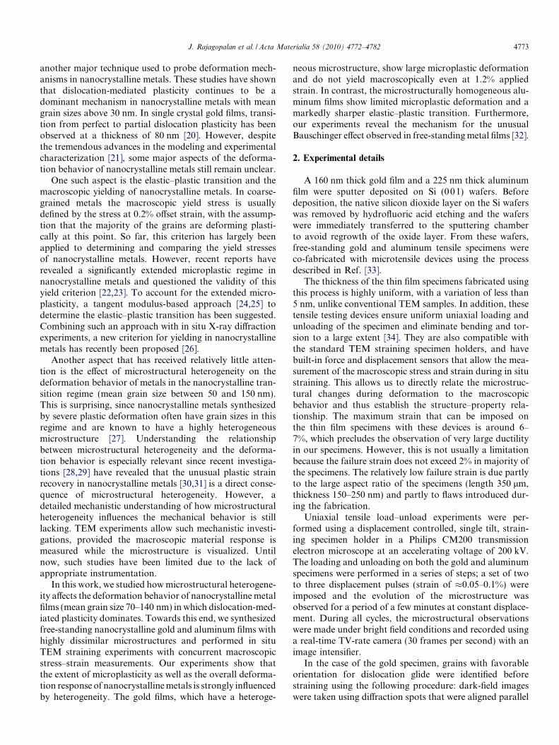
The microstructure of the thin film specimens wereexamined using TEM and X-ray diffraction. The gold filmdid not show epitaxial growth and had a fairly heteroge-neous microstructure (Fig. 1a), with a weak [111] texturein the film growth direction and a uniform in-plane texture.The average grain size (dm) was 70 nm, but some very smallgrains (<0.2dm) and some fairly large grains (�2.5dm) werealso present (Fig. 1b). Such a wide distribution of grainsizes has been observed previously in other nanocrystallinemetals and alloys [35].
Fig. 1. Bright-field transmission electron micrograph (a) and histogram of the gmicrograph (c) and histogram of the grain size distribution (d) of the aluminumwith respect to each other. The corresponding diffraction patterns (shown as i
The aluminum film (dm = 120 nm) showed a less pro-nounced variation (Fig. 1d) between the smallest grains(�0.5dm) and the largest (�2.5dm). More importantly, thefilm showed epitaxial growth [36] with the following rela-tionships: Al(110)kSi(0 01), Al[001]kSi[110] andAl(110)kSi(00 1), Al[00 1]kSi½1�10�. In other words, the filmhad a fairly homogeneous microstructure with a strong(11 0) out-of-plane texture and only two in-plane grain ori-entations, rotated 90� in-plane with respect to each other.Because the tensile loading axis was aligned with the[00 1] direction of one set of grains and the ½1�1 0� directionof the other set, all the grains had several [110]{111} slipsystems with an identical Schmid factor of 0.408. This dras-tically reduced the plastic incompatibilities that can arisefrom variations in resolved shear stresses in differentgrains.
4. Experimental results
4.1. In situ TEM deformation of nanocrystalline gold film
with heterogeneous microstructure
The stress–strain response of the gold film during in situTEM deformation is shown in Fig. 2a. In the first two
rain size distribution (b) of the gold film. Bright-field transmission electronfilm. The aluminum film has only two (110) growth variants, rotated 90�
nsets in (a) and (c)) reveal the different texture of the two films.

0
50
100
150
200
250
300
350
0 0.2 0.4 0.6 0.8 1 1.2
Stre
ss (M
Pa)
Strain (%)
Cycle 1Cycle 2Cycle 3
a
b
c
a Au
0
50
100
150
200
250
300
350
400
0 0.2 0.4 0.6 0.8 1 1.2 1.4 1.6 1.8 2
Stre
ss (M
pa)
Strain (%)
Cycle 1Cycle 2
b Al
Fig. 2. (a) The stress–strain measurements for the gold film during in situTEM deformation. Note that the stress–strain curves deviate from theelastic unloading path (indicated by dashed black lines) during all threedeformation cycles. In the first and second cycles, stress–strain measure-ments were made at only a few points, whereas the third cycle wasrecorded in more detail. The microstructural changes that accompanystrain increments/decrements during stages a–c of the third deformationcycle are shown in Fig. 4 (see text for details). (b) The stress–strainmeasurements for the aluminum film during in situ TEM deformation,showing a fairly sharp elastic–plastic transition.
J. Rajagopalan et al. / Acta Materialia 58 (2010) 4772–4782 4775
deformation cycles, we focused mainly on identifying thedeformation mechanisms and qualitatively observing themicrostructural changes. During the third cycle, stress–strain measurements were made regularly to correlate thechanges in the microstructure with the macroscopic behav-ior. The measurements provide direct evidence of the mac-roscopic Bauschinger effect, as seen by the pronounceddeviation of the stress–strain response from elastic behav-ior during unloading.
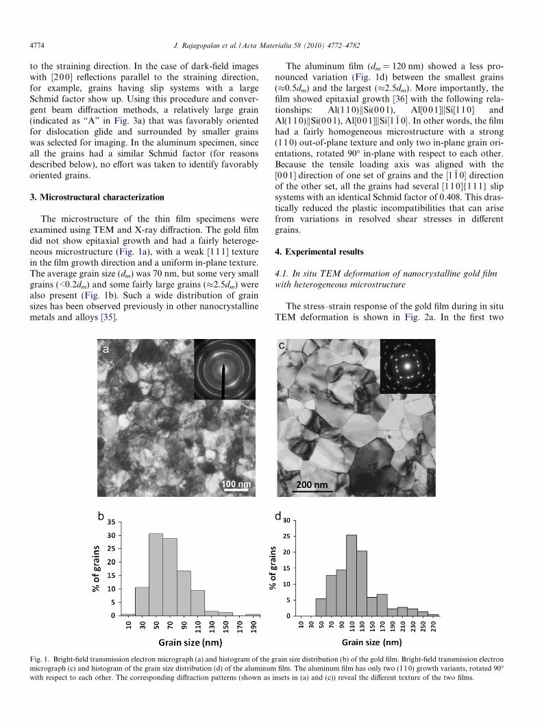
Fig. 3 shows the time evolution of the microstructure inthe gold specimen after the application of a set of deforma-tion pulses towards the end of loading in the third cycle(for the corresponding movie, see Video S1; note that thisvideo, as well as Videos S2, S3 and S4, are played at fourtimes the actual speed). As evident from the images, dislo-cation-induced changes in contrast (indicated by redarrows) were confined to only a few grains, with especially
high activity in the large grain in the middle. No noticeabledislocation activity was seen in most of the smaller grains,which indicates that the smaller grains are deforming elas-tically (for more evidence of such elastic–plastic deforma-tion see Video S2). In other words, the gold specimenshows microplastic deformation even though the plasticstrain induced in this cycle (>0.3%) is well above the con-ventional 0.2% limit for the macroplastic transition. It islikely, however, that the dislocation activity in some ofthe smaller grains was missed due to unfavorable diffrac-tion conditions or the short time scales for dislocationmotion in them.
Furthermore, even with the applied displacement heldconstant, dislocation bursts continued to occur severalminutes after the initial deformation pulse. This phenome-non, which was seen during all three deformation cycles,indicates a thermal dependence of dislocation propagationby depinning events and may explain the high strain ratesensitivity observed in nanocrystalline metals [10]. Thesequence of video frames shown in Fig. 3d–f shows thenucleation and propagation of a dislocation from the upperleft GB of the large grain. During its propagation, this dis-location gets pinned at one of its ends and further propaga-tion occurs upon depinning. Such time-dependentdepinning of dislocations at GBs has been observed previ-ously in MD simulations and was shown to be a thermallyactivated process [37]. We note that in all our analysis onlysudden contrast changes, as opposed to changes caused byelastic distortions, were interpreted as a signature of dislo-cation activity. In most cases, these sudden contrastchanges were accompanied by visible motion ofdislocations.
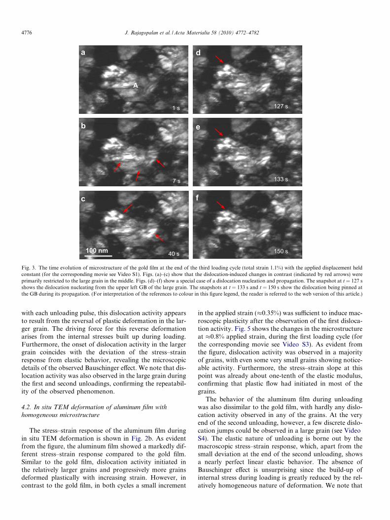
This extended microplasticity during loading offers astraightforward explanation for the Bauschinger effect seenduring unloading. During the initial stages of loading(Fig. 4a) there were no changes in contrast in any of thegrains, indicating that the deformation is primarily elastic.However, with increasing strain sudden changes in con-trast, frequently accompanied by visible motion of individ-ual dislocations, were observed in the larger grain (Fig. 4b)but were largely absent in the surrounding smaller grains.Furthermore, the onset of dislocation activity in the largergrain coincides with a reduction in the macroscopic stress–strain slope, which suggests that the apparent high strainhardening is just a manifestation of this elastic–plasticdeformation. More importantly, the plastic relaxationleads to a lower stress level in the larger grain as comparedto its elastically deforming neighbors, leading to a build-upof internal stresses.
During the initial phase of unloading, contrast changeswere not seen in any of the grains, which is consistent withthe observed elastic stress–strain response. However, uponfurther unloading, the dislocation configuration in the lar-ger grain became unstable and noticeable dislocation activ-ity was seen after an unloading pulse (Fig. 4c). Similardislocation activity was observed intermittently as theunloading progressed. Since the macroscopic stress reduces
a
b
1 s
7 s
c
40 s
d
e
f
127 s
133 s
150 s100 nm
A
Fig. 3. The time evolution of microstructure of the gold film at the end of the third loading cycle (total strain 1.1%) with the applied displacement heldconstant (for the corresponding movie see Video S1). Figs. (a)–(c) show that the dislocation-induced changes in contrast (indicated by red arrows) wereprimarily restricted to the large grain in the middle. Figs. (d)–(f) show a special case of a dislocation nucleation and propagation. The snapshot at t = 127 sshows the dislocation nucleating from the upper left GB of the large grain. The snapshots at t = 133 s and t = 150 s show the dislocation being pinned atthe GB during its propagation. (For interpretation of the references to colour in this figure legend, the reader is referred to the web version of this article.)
4776 J. Rajagopalan et al. / Acta Materialia 58 (2010) 4772–4782
with each unloading pulse, this dislocation activity appearsto result from the reversal of plastic deformation in the lar-ger grain. The driving force for this reverse deformationarises from the internal stresses built up during loading.Furthermore, the onset of dislocation activity in the largergrain coincides with the deviation of the stress–strainresponse from elastic behavior, revealing the microscopicdetails of the observed Bauschinger effect. We note that dis-location activity was also observed in the large grain duringthe first and second unloadings, confirming the repeatabil-ity of the observed phenomenon.
4.2. In situ TEM deformation of aluminum film withhomogeneous microstructure
The stress–strain response of the aluminum film duringin situ TEM deformation is shown in Fig. 2b. As evidentfrom the figure, the aluminum film showed a markedly dif-ferent stress–strain response compared to the gold film.Similar to the gold film, dislocation activity initiated inthe relatively larger grains and progressively more grainsdeformed plastically with increasing strain. However, incontrast to the gold film, in both cycles a small increment
in the applied strain (�0.35%) was sufficient to induce mac-roscopic plasticity after the observation of the first disloca-tion activity. Fig. 5 shows the changes in the microstructureat �0.8% applied strain, during the first loading cycle (forthe corresponding movie see Video S3). As evident fromthe figure, dislocation activity was observed in a majorityof grains, with even some very small grains showing notice-able activity. Furthermore, the stress–strain slope at thispoint was already about one-tenth of the elastic modulus,confirming that plastic flow had initiated in most of thegrains.
The behavior of the aluminum film during unloadingwas also dissimilar to the gold film, with hardly any dislo-cation activity observed in any of the grains. At the veryend of the second unloading, however, a few discrete dislo-cation jumps could be observed in a large grain (see VideoS4). The elastic nature of unloading is borne out by themacroscopic stress–strain response, which, apart from thesmall deviation at the end of the second unloading, showsa nearly perfect linear elastic behavior. The absence ofBauschinger effect is unsurprising since the build-up ofinternal stress during loading is greatly reduced by the rel-atively homogeneous nature of deformation. We note that
40 s
50 s
a
25 s
b
c
100 nm
Fig. 4. The evolution of microstructure of the gold film during the different stages of the third deformation cycle. Figs. (a)–(c) correspond to the stages a–cindicated in Fig. 2a, respectively. Green and yellow arrows indicate the direction of loading and unloading, respectively. The figure on the left side showsthe microstructure just before the application of the displacement pulses at each stage. The figure on the right side shows the microstructure after theapplication of the displacement pulses. The time difference is indicated in the right side figures. Clear changes in contrast (indicated by red arrows) wereobserved in the later stages of both loading (b) and unloading (c). On the other hand, very few changes in dislocation contrast were observed during theearly stages of loading (a) as well as unloading. (For interpretation of the references to colour in this figure legend, the reader is referred to the web versionof this article.)
J. Rajagopalan et al. / Acta Materialia 58 (2010) 4772–4782 4777
there was no stress-assisted grain growth in this aluminumfilm during deformation, unlike the films in Ref. [12], pos-sibly because of the columnar structure of the grains as wellas the small applied strain. However, we observed graingrowth in another aluminum film with a smaller grain size(dm = 100 nm) when it was deformed to about 6% strain(data not shown).
4.3. Deformation of aluminum film with heterogenous
microstructure
In addition to in situ TEM experiments, we also per-formed ex situ deformation experiments on another alumi-num film. This aluminum film had a thickness (215 nm)and mean grain size (140 nm) similar to those of the alumi-num film described in Section 4.2. However, in contrast tothe highly textured aluminum film, this film did not haveany preferred out-of-plane or in-plane texture (Fig. 6a).This non-textured film was synthesized by sputter deposit-ing aluminum on a Si (001) wafer with the native oxide
layer intact. The oxide layer disrupts the epitaxial growthand, as a result, the aluminum film does not have any pre-ferred texture. The stress–strain response of this non-tex-tured aluminum film is shown in Fig. 6c. As evident fromthe figure, this microstructurally heterogeneous aluminumfilm showed a gradual elastic–plastic transition and a sub-stantial Bauschinger effect during unloading. These resultsclearly show that differences in microstructural heterogene-ity alone can cause significant variation in the deformationbehavior of nanocrystalline metals even if they have similarmean grain sizes.
5. Discussions
As mentioned earlier, nanocrystalline metals are expectedto deform heterogeneously [38] and only a small fraction ofgrains undergo plastic events at the conventionally definedmacroyield point [39]. To account for the extendedmicroplasticity and to map the elastic–plastic transition insuch heterogeneously deforming materials, a tangent

0 s
30 s
80 s
130 s
310 s
380 s
480 s
550 s
200 nm
Fig. 5. The time evolution of the microstructure of the aluminum film at about 0.8% applied strain (first loading cycle). Dislocation activity could be seenin most of the grains at this stage (for the corresponding movie see Video S3).
4778 J. Rajagopalan et al. / Acta Materialia 58 (2010) 4772–4782
modulus-based approach was developed. This method wasused to analyze the deformation of Cu–Cr composite wires[24], and was later extended to thin films and multilayers[25]. Based on this analysis, it was concluded that the mic-rodeformation stage in most fine-grained polycrystalsgreatly exceeded the 0.2% strain criterion.
Recently, the deformation behavior of Cu/Nb compos-ite wires was examined in a series of studies [40–42] througha combination of macroscopic tensile experiments andin situ diffraction experiments. The Cu/Nb wires nominallyconsisted of three “phases” – a large-Cu phase, comprisinggrains ranging from a few hundred nanometers to several
microns; a fine-Cu phase, comprising grains of a few tensto a few hundred nanometers; and Nb nanotubes/nanofila-ments – and showed a macroscopic Bauschinger effect dur-ing unloading. The analysis of the in situ experiments usingthe tangent modulus approach revealed the presence ofphase-specific elasto-plastic regimes and showed that theBauschinger effect is the result of macroscopic yielding ofthe large-Cu phase in compression during unloading [26].Furthermore, it was found that the elastic strain to totalstrain ratio in the large-Cu phase at its macroscopic yield-ing, in both tension and compression, was 0.33. Based onthis insight, it was proposed that the macroyield stress be

200 nm
a
0
5
10
15
20
25
30
10 30 50 70 90 110
130
150
170
190
210
230
250
270
290
310
330
350
% o
f gra
ins
Grain size (nm)
b
0
50
100
150
200
250
300
0 0.2 0.4 0.6 0.8 1 1.2 1.4 1.6
Stre
ss (M
pa)
Strain (%)
Cycle 1
Cycle 2
c
Fig. 6. Bright-field transmission electron micrograph (a) and histogram ofgrain sizes (b) of the non-textured aluminum film (thickness 215 nm,dm = 140 nm). The diffraction pattern (shown as the inset in (a)) revealsthe lack of any preferred texture. (c) Stress–strain measurements for thealuminum film during two cycles. The film shows a gradual elastic–plastictransition during loading and a substantial Bauschinger effect duringunloading. The elastic unloading path is indicated by the dashed blacklines.
dσσ
a b
F
Fig. 7. (a) Idealized microstructure used for modeling the effect ofmicrostructural heterogeneity. (b) Equivalent representation of themicrostructure in terms of springs and sliding elements. Each spring–slider pair represents a grain. The pairs with larger sliding elementsrepresent grains with high yield stress and vice versa.
J. Rajagopalan et al. / Acta Materialia 58 (2010) 4772–4782 4779
defined as the point at which the macroscopic work hard-ening rate (tangent modulus), h = dr/d�, becomes less thanone-third of the Young’s modulus.
The tangent modulus approach to determine the macro-yield point of nanocrystalline metals is intuitively appealingsince it takes into account their gradual elastic–plastic tran-sition. Our in situ TEM experiments suggest that a crite-
rion for macroplastic transition should take into accountan additional factor, namely the heterogeneity of themicrostructure. The microstructurally heterogenous goldfilm undergoes only microplastic deformation in all threecycles and as a result shows a pronounced Bauschingereffect. This is the case even at the end of the third loading,where the macroscopic work hardening rate is less thanone-quarter of the Young’s modulus. On the other hand,the microstructurally homogeneous aluminum film, despitehaving a comparable mean grain size, exhibits a fairlysharp elastic–plastic transition – an increment in appliedstrain of around 0.35% after the onset of microplasticityis sufficient to induce macroplasticity in both cycles. Thistransition to macroplasticity is confirmed by the reductionin the macroscopic work hardening rate to about one-tenthof the Young’s modulus. We also performed additionalin situ TEM straining experiments on other Al films withhomogeneous microstructure to verify the observationsreported here. These studies unambiguously confirmed thata relatively homogenous microstructure leads to a reduc-tion in microplastic deformation as well as Bauschingereffect during unloading.
The effect of an inhomogeneous microstructure on thestress–strain response can be understood in terms of thesimple one-dimensional model shown in Fig. 7a. The modelidealizes the microstructure as a collection of grains ofdifferent sizes, all of which are under the same strain (equalto the macroscopic strain) at any point during loading orunloading. An equivalent representation of such a micro-structure in terms of springs and sliding elements is shownin Fig. 7b. Each spring–slider pair represents a grain. Theextension of the springs represents elastic deformation inthe grains while the motion of the sliders represents plasticdeformation. All the springs have equal stiffness, butgreater force is required to move larger sliding elements.In effect, spring–slider pairs with larger sliding elementsrepresent grains with high yield stress and vice versa. Tocalculate the uniaxial stress–strain response of such a sys-tem, we further assume that

4780 J. Rajagopalan et al. / Acta Materialia 58 (2010) 4772–4782
1. The grains have the stress–strain characteristics of anelastic–perfectly plastic material, that is, there is nostrain hardening.
2. The yield stress of the grains is the same in both ten-sion and compression.
Based on these assumptions, the normal stress incrementin grain i due to a macroscopic strain increment d� duringloading is given by
dri ¼Ed� ri < ryi
0 ri P ryi
�ð1Þ
Here ryi is the tensile yield stress of grain i and E is theYoung’s modulus. The stress decrement in grain i due toa macroscopic strain decrement during unloading is gi-ven by
dri ¼Ed� ri > �ryi
0 ri 6 �ryi
�ð2Þ
The macroscopic stress at any point during loading orunloading is given by the weighted average of the stres-ses in the individual grains. Therefore,
r ¼P
ridiPdi
ð3Þ
where di is the size of grain i. We now use this simple modelto simulate the uniaxial stress–strain response of the225 nm thick textured aluminum film (Fig. 2b) and the215 nm thick non-textured aluminum film (Fig. 6c). Inthese simulations, we use the actual grain size distributionof the films shown in Fig. 1d and Fig. 6b, respectively.
To simulate the stress–strain response, we first assignyield stresses to individual grains in the following way.Since the mean grain sizes (dm) of these films fall in thenanocrystalline transition regime (around 100 nm), weassume that grains that are larger than dm have pre-exist-ing dislocation sources, the size of which scale as the grainsize. Since the shear stress required to activate a disloca-tion source is inversely proportional to its size, the criticalresolved shear stress for these grains is inversely propor-tional their size di. However, the stress at which a grainyields also depends on its orientation with respect to thestraining direction, i.e. the Schmid factor (m) of the slipsystems in the grain. Typically, m is different for differentslip systems and the system with the highest m gets acti-vated first. However, depending on the grain orientation,up to five independent slip systems may be required toaccommodate the imposed strain purely through slip [1].For simplicity, we therefore assume that a grain yieldsonly when the applied stress is sufficient to activate at leastfive slip systems in the grain. If fewer than five slip systemshave a non-zero m, we assume that the grain yields whenthe least favorable system is activated. Hence, the yieldstress of the grains is dictated by the m of the least favor-able slip system required to accommodate the imposedstrain.
For grains smaller than dm we assume that plasticity iscontrolled by nucleation of dislocations from grain bound-aries and is independent of the grain size. Therefore, weassign yield stress values for these smaller grains randomlyfrom a uniform distribution with a lower limit of rnl and anupper limit of rnu.
We first consider the textured Al film which has only twomajor grain orientations. The grains whose [001] directionis aligned with the loading axis have eight slip systems withnon-zero m. The other set of grains have four such slip sys-tems. However, the Schmid factor of all the slip systems inboth sets of grains is identical (mt = 0.408). Therefore, theuniaxial yield stress of grains larger than dm (120 nm) canbe represented simply by
ryi ¼C
mtdidi > 120 nm ð4Þ
where C is a constant. The non-textured film has a slightlylarger mean grain size (dm = 140 nm) and the orientation ofthe grains vary. Therefore, for the non-textured film
ryi ¼D
mididi > 140 nm ð5Þ
where D is a constant and mi is the Schmid factor associatedwith grain i. Since the grains are randomly oriented, wechose mi from a uniform distribution with a range of 0.1–0.4. The limits 0.1 and 0.4 are conservative since there aregrain orientations for which the m of the least favorable slipsystem is outside these limits. The macroscopic stress–strainresponse is then calculated using Eqs. (1)–(3). Fig. 8 showsthe typical response for the textured and non-textured filmobtained from the simulations. For both the films,approximately 12,000 grains were used for simulating thestress–strain behavior. For these simulations, C = 10 N/m,D = 5 N/m, rnl = 250 MPa and rnu = 750 MPa. These val-ues were chosen so that the maximum stress obtained inthe simulations was similar to the experiments. Changingthese parameters leads to variation in the magnitude of thecalculated stresses, but the qualitative stress–strain responseremains similar.
As evident from Fig. 8, the textured film shows very littleBauschinger effect during both the cycles, which is consis-tent with the experimentally observed response (Fig. 2b).This is the case because, even though there is variation inry among the grains due to their size, it is sufficient to inducereverse yielding in only a few larger grains during unload-ing. On the other hand, the non-textured film shows anoticeable Bauschinger effect in both cycles, which is consis-tent with the experimentally observed behavior (Fig. 6c). Inthe non-textured film, the variation in ry comes from boththe grain size and the orientation (m). This leads to a sub-stantially more heterogeneous stress distribution duringloading. As a result, reverse yielding occurs in a significantfraction of large/favorably oriented grains during unload-ing, leading to a substantial Bauschinger effect.
Note that the stress–strain curves shown in Fig. 8 corre-sponds to a particular simulation. Because the yield stresses

a
b
0 0.3 0.6 0.9 1.2 1.50
50
100
150
200
250
300
350
Strain (%)
Stre
ss (M
Pa)
Cycle 1Cycle 2
0 0.3 0.6 0.9 1.2 1.50
50
100
150
200
250
300
350
Strain (%)
Stre
ss (M
Pa)
Cycle 1Cycle 2
Fig. 8. Simulated stress–strain curves for the 225 nm thick textured Alfilm (a) and the 215 nm thick non-textured Al film (b). The textured filmshows only a small Bauschinger effect in both cycles, whereas the non-textured film shows a substantial Bauschinger effect.
J. Rajagopalan et al. / Acta Materialia 58 (2010) 4772–4782 4781
of grains smaller than dm are assigned randomly, there is avery small variation in the response from simulation tosimulation. In the case of the non-textured film there is aslightly larger variation, since the yield stress of largergrains is also chosen randomly (Eq. (5)). Typically, theBauschinger effect is most pronounced in the non-texturedfilm when the relatively larger grains have high m and viceversa. However, the overall response is very similar fromsimulation to simulation. In addition, as the number ofgrains used in the simulations becomes higher the variationbecomes negligible.
In this simple model, only variations in yield stress aris-ing from the distribution of grain sizes and orientationwere considered. However, in real experimental samplesyielding in different grains can be affected, among otherfactors, by differences in the grain boundary structureand density of pre-existing dislocations, and therefore amore heterogeneous stress distribution is likely. Also,grains may have lower yield stress in compression if theyhave deformed plastically in tension. Both these effects willlead to a more pronounced Bauschinger effect. Despite themany simplifying assumptions used, the model captures the
effect of microstructural heterogeneity on the stress–strainresponse reasonably well. Along with the insights providedby the in situ TEM observations, these results clearly dem-onstrate the critical role of heterogeneity in shaping themechanical behavior of nanocrystalline metals.
6. Conclusions
In this study, we performed quantitative in situ TEMstraining experiments on free-standing gold and aluminumfilms to explore the role of microstructural heterogeneity inthe deformation behavior of nanocrystalline metals. Thegold film, which has a fairly heterogenous microstructure,with randomly oriented grains and a wide distribution ofgrain sizes, showed extensive microplasticity and a pro-nounced Bauschinger effect during unloading. Similarbehavior was also seen in aluminum films with a heteroge-neous microstructure. Microstructurally homogeneous alu-minum films, in contrast, exhibited limited microplasticdeformation and a very small Bauschinger effect despite acomparable mean grain size. A simple model that incorpo-rate the heterogeneity of the microstructure was used tosimulate the stress–strain behavior of the aluminum films.The simulations confirmed that the extended microplastic-ity and Bauschinger effect are the result of an inhomoge-neous stress distribution (high stresses in elasticallydeforming grains, low stresses in plastically deforminggrains) caused by microstructural heterogeneity. Theseresults strongly argue against a purely grain size-centricdescription of plasticity in nanocrystalline metals andemphasize the need to take into account both the micro-structural size and the heterogeneity.
Acknowledgements
This material is based upon work supported by theNational Science Foundation under Award No. NSFECS-0304243 and Award No. NSF CMMI-0728189. Thegold and aluminum specimens were fabricated in theMicro-nano-mechanical Systems Cleanroom and MicroNano Technology Laboratory at the University of Illinoisat Urbana-Champaign. The in situ TEM experiments wereperformed at the University of Vienna, supported by theresearch focus “Materials Science – Functional Materialsand Nanostructures”. We thank Prof. Hael Mughrabi(University of Erlangen) for valuable discussions.
Appendix A. Supplementary material
Supplementary data associated with this article can befound, in the online version, at doi:10.1016/j.actamat.2010.05.013.
References
[1] Hirth JH, Lothe J. Theory of dislocations. New York: Wiley-Interscience; 1982.
4782 J. Rajagopalan et al. / Acta Materialia 58 (2010) 4772–4782
[2] Legros M, Elliot BR, Rittner MN, Weertman JR, Hemker KJ. PhilosMag A 2000;80:1017–26.
[3] Haque MA, Saif MTA. J Mater Res 2005;20:1769–77.[4] Lu L, Sui ML, Lu K. Science 2000;287:1463–6.[5] Legros M, Gianola DS, Hemker KJ. Acta Mater 2008;56:3380–93.[6] Wu XL, Zhu YT, Ma E. Appl Phys Lett 2006;88:121905.[7] Wang YB, Li BQ, Sui ML, Mao SX. Appl Phys Lett 2008;92:011903.[8] Meyers M, Mishra A, Benson D. Prog Mater Sci 2006;51:427–556.[9] Schwaiger R, Moser B, Dao M, Chollacoop N, Suresh S. Acta Mater
2003;51:5159–72.[10] Wang YM, Hamza AV, Ma E. Acta Mater 2006;54:2715–26.[11] Zhang K, Weertman JR, Eastman JA. Appl Phys Lett 2005;87:061921.[12] Gianola DS, Van Petegem S, Legros M, Brandstetter S, Van
Swygenhoven H, Hemker KJ. Acta Mater 2006;54:2253–63.[13] Schiotz J, Jacobsen KW. Science 2003;301:1357–9.[14] Yamakov V, Wolf D, Phillpot SR, Mukherjee AK, Gleiter H. Nat
Mater 2004;3:43–7.[15] Swygenhoven HV, Derlet PM, Froseth AG. Nat Mater
2004;3:399–403.[16] Swygenhoven HV. Mater Sci Eng A 2008;483–484:33–9.[17] Hugo RC, Kung H, Weertman JR, Mitra R, Knapp JA, Follstaedt D.
Acta Mater 2003;51:1937–43.[18] Kumar KS, Suresh S, Chisholm MF, Horton JA, Wang P. Acta
Mater 2003;51:387–405.[19] Robertson IM, Ferreira P, Dehm G, Hull R. MRS Bull 2008;33/
2:122–31.[20] Oh SH, Legros M, Kiene D, Gruber P, Dehm G. Acta Mater
2007;55:5558–71.[21] Kumar KS, Van Swygenhoven H, Suresh S. Acta Mater 2003;51:5743–74.[22] Brandstetter S, Swygenhoven HV, Petegem SV, Schmitt B, MaaB R,
Derlet PM. Adv Mater 2006;18:1545–8.
[23] Li H, Choo H, Ren Y, Saleh TA, Lienert U, Liaw PK, et al. Phys RevLett 2008;101:015502.
[24] Sinclair CW, Saada G, Embury JD. Philos Mag 2006;86:4081–98.[25] Saada G, Verdier M, Dirras GF. Philos Mag 2007;87:4875–92.[26] Thilly L, Petegem SV, Renault P-O, Lecouturier F, Vidal V, Schmitt
B, et al. Acta Mater 2009;57:3157–69.[27] Valiev R, Islamgaliev R, Alexandrov I. Prog Mater Sci
2000;45:103–89.[28] Lonardelli I, Almer J, Ischia G, Menapace C, Molinari A. Scr Mater
2009;60:520–3.[29] Li X, Wei Y, Yang W, Gao H. Proc Natl Acad Sci USA
2009;106:16108–13.[30] Rajagopalan J, Han JH, Saif MTA. Science 2007;315:1831–4.[31] Rajagopalan J, Han JH, Saif MTA. Scr Mater 2008;59:921–6.[32] Rajagopalan J, Han JH, Saif MTA. Scr Mater 2008;59:734–7.[33] Han JH, Saif MTA. Rev Sci Instrum 2006;77:045102.[34] Haque MA, Saif MTA. Expt Mech 2002;42:123–8.[35] Rentenberger C, Waitz T, Karnthaler HP. Scr Mater 2004;51:
789–94.[36] Niwa H, Kato M. Appl Phys Lett 1991;59:543–5.[37] Van Swygenhoven H, Derlet PM, Froseth A. Acta Mater
2006;54:1975–83.[38] Bitzek E, Derlet P, Anderson P, Swygenhoven HV. Acta Mater
2008;56:4846–57.[39] Saada G. Mater Sci Eng A 2005;400–401:146–9.[40] Thilly L, Renault P-O, Vidal V, Lecouturier F, Petegem SV, Stuhr U,
et al. Appl Phys Lett 2006;88:191906.[41] Thilly L, Renault PO, Petegem SV, Brandstetter S, Schmitt B,
Swygenhoven HV, et al. Appl Phys Lett 2007;90:241907.[42] Vidal V, Thilly L, Petegem SV, Stuhr U, Lecouturier F, Renault P-O,
et al. Scr Mater 2009;60:171–4.