in-field built-in self-test for measuring rf transmitter ... · doohwang chang and koushik malladi...
TRANSCRIPT

In-field Built-in Self-test for Measuring RF Transmitter Power and Gain
by
Sudheer Kumar Reddy Gangula
A Thesis Presented in Partial Fulfillment
of the Requirements for the Degree
Master of Science
Approved November 2015 by the
Graduate Supervisory Committee:
Jennifer Kitchen, Chair
Sule Ozev
Umit Ogras
ARIZONA STATE UNIVERSITY
December 2015
i
ABSTRACT
RF transmitter manufacturers go to great extremes and expense to ensure that their
product meets the RF output power requirements for which they are designed. Therefore,
there is an urgent need for in-field monitoring of output power and gain to bring down the
costs of RF transceiver testing and ensure product reliability. Built-in self-test (BIST)
techniques can perform such monitoring without the requirement for expensive RF test
equipment. In most BIST techniques, on-chip resources, such as peak detectors, power
detectors, or envelope detectors are used along with frequency down conversion to analyze
the output of the design under test (DUT). However, this conversion circuitry is subject to
similar process, voltage, and temperature (PVT) variations as the DUT and affects the
measurement accuracy. So, it is important to monitor BIST performance over time, voltage
and temperature, such that accurate in-field measurements can be performed.
In this research, a multistep BIST solution using only baseband signals for test
analysis is presented. An on-chip signal generation circuit, which is robust with respect to
time, supply voltage, and temperature variations is used for self-calibration of the BIST
system before the DUT measurement. Using mathematical modelling, an analytical
expression for the output signal is derived first and then test signals are devised to extract
the output power of the DUT. By utilizing a standard 180nm IBM7RF CMOS process, a
2.4GHz low power RF IC incorporated with the proposed BIST circuitry and on-chip test
signal source is designed and fabricated. Experimental results are presented, which show
this BIST method can monitor the DUT’s output power with +/- 0.35dB accuracy over a
20dB power dynamic range.

ii
To my parents and family

iii
ACKNOWLEDGMENTS
I would like to express my appreciation and thanks to my supervisors Dr. Jennifer
Kitchen and Dr. Sule Ozev, for their support, guidance, and friendly attitude during my
graduate study and the development of this thesis. I also thank my committee member Dr.
Umit Ogras for his time and effort to help me fulfill the degree requirements.
I would like to thank my colleagues Soroush Moallemi, Jae Woong Jeong,
Doohwang Chang and Koushik Malladi for their support, help and great friendship. Thanks
to James Laux for his support in software and system issues.
I would like to thank to my parents and my sister, for their patience, support, and
encouragement throughout my Masters. Lastly, I would like to thank all my classmates and
friends for their support, friendship and fun time.

iv
TABLE OF CONTENTS
Page
LIST OF TABLES ................................................................................................................... vi
LIST OF FIGURES ............................................................................................................... vii
CHAPTER
1 INTRODUCTION ....................................................................................................... 1
1.1 Outline of Thesis ................................................................................. 1
1.2 Prior Work ............................................................................................ 2
2 BIST SYSTEM AND METHODOLOGY ................................................................ 7
2.1 System Model ...................................................................................... 7
2.2 Calibration Phase ............................................................................... 10
2.3 Measurement Phase ........................................................................... 12
3 CIRCUIT DESIGN AND IMPLEMENTATION ................................................... 15
3.1 BIST Signal Source............................................................................ 16
3.2 Directional Coupler ............................................................................ 19
3.3 SPDT RF Switch ................................................................................ 21
3.4 Down Conversion Mixer ................................................................... 22
3.5 LO VCO ............................................................................................. 24
3.5 Chip Integration and Top Level Routing .......................................... 25
4 MEASUREMENT RESULTS ..................................................................................27
4.1 Testing of BIST Signal Source .......................................................... 29
4.2 Calibration Phase ............................................................................... 32
4.3 Measurement Phase ........................................................................... 33

v
CHAPTER Page
5 CONCLUSION AND FUTURE WORK ................................................................ 37
REFERENCES.......................................................................................................................38

vi
LIST OF TABLES
Table Page
1. BIST Parameter Descriptions ............................................................................... 10
2. Area Overhead of the BIST System .................................................................... 26
3. GPATH Loss Results ................................................................................................ 29
4. BIST Source Amplitude and GBIST with Voltage Variation................................. 30
5. BIST Source Amplitude and GBIST with Temperature Variation ......................... 31
6. Calculated vs Measured Power Comparison ........................................................ 35

vii
LIST OF FIGURES
Figure Page
1. Pre-Distortion Scheme for CMOS PA ............................................................ 2
2. LUT based Power Detection ........................................................................... 3
3. Loopback Test Setup for RF Transceiver ...................................................... 5
4. RF Transmitter with BIST Monitoring System ............................................. 7
5. Block Diagram Showing Down Conversion Scheme .................................... 8
6. Proposed BIST Monitoring System ................................................................ 9
7. Monitoring System Showing Calibration Path ............................................ 11
8. Monitoring System Showing Measurement Path ......................................... 13
9. BIST Monitoring System Circuit Implementation ...................................... 15
10. LC Oscillator with Amplitude Control Loop .............................................. 18
11. Output Amplitude Settling of LC Oscillator ............................................... 19
12. Schematic of Directional Coupler ............................................................... 20
13. Input Matching and Coupling of Directional Coupler ................................ 20
14. Schematic of Single Pole Double Throw Switch ....................................... 21
15. S-Parameters of SPDT Switch over 2-3GHz Range ................................... 22
16. Schematic of Differential Gilbert Cell Mixer ............................................. 23
17. Linearity of Mixer ....................................................................................... 23
18. Schematic of LO VCO ................................................................................. 24
19. Frequency Tuning Range of LO VCO ....................................................... 25
20. Chip Die Microphotograph .......................................................................... 26
21. Evaluation PCB ............................................................................................ 27

viii
Figure Page
22. Hardware Setup for Path Loss Calibration ................................................. 28
23. Evaluation Board Path Loss Diagram ......................................................... 28
24. BIST Source Amplitude and GBIST over Voltage ....................................... 30
25. BIST Source Amplitude and GBIST over Temperature ............................... 31
26. Hardware Setup for Calibration Phase ........................................................ 32
27. Hardware Setup for Measurement Phase .................................................... 33
28. Injected vs BIST Computed Power at Nominal and Voltage Corner ........ 35
29. Injected vs BIST Computed Power at Temperature and VT Corner ......... 36
1
CHAPTER 1
INTRODUCTION
Wireless communications is the fastest growing segment of the communication
industry with currently 7400 million mobile subscriptions worldwide and forecasted to
have 9100 million subscriptions by 2021 [1]. With the exponential increase in the mobile
phone usage, reducing power consumption and cost of the device are of the utmost
importance. Recent advances in semiconductor technologies have allowed for high scale
integration of complete systems on a single chip. As higher levels of integration continue,
digital-centric silicon CMOS technologies have emerged as viable processes for Radio
Frequency (RF) integrated circuits.
However, as the process scales down, the supply voltages and device breakdowns
also decrease. Smaller feature size makes the device vulnerable to process, voltage, and
temperature (PVT) variations. Being the most crucial block in the transmitter, the power
amplifier (PA) is designed to have high efficiency and to deliver high power to the antenna.
Efficiency, output power and linearity of power amplifiers drastically change in the field
with temperature, ageing, and supply voltage [2], [3]. To ensure the quality over PVT
variations, on-chip test and calibration of RF transceiver SoCs appear to be a must for near-
future wireless transceivers.
1.1 Outline of Thesis:
This thesis consists of five chapters. The first chapter presents a brief overview of
the in-field monitoring of RF transmitters, different output power detection techniques, and
BIST methods for RF systems and their importance. The second chapter introduces the

2
proposed BIST technique for in-field monitoring of the design under test (DUT), describing
the system level model and theoretical equations. In the third chapter, the circuit
implementation of this BIST system is discussed in detail. Chapter Four demonstrates the
evaluation of this BIST system with hardware measurement results. Chapter Five finally
summarizes this work.
1.2 Prior Work:
In a communication system, the information sent from the transmitter is decoded to
amplitude and phase at the receiver. Any imperfection in the transmitter, especially in the
power amplifier, will result in symbol deviation, which causes error in signal information.
These non-idealities lead to AM/AM and AM/PM distortions and finally increase the Error
Vector Magnitude (EVM) of transmitters. So output monitoring and correction schemes to
improve different specifications is crucial in RF transmitters. In this section different output
detection and correction methods from prior work are shown and discussed.
PA
Digital Predistortion
Power Ctrl
VGADAC
RF Transmitter
Up conversion
LO
Down conversion
ADC
Fig. 1. Pre-Distortion Scheme for CMOS PA

3
A widely used method to improve the power amplifier linearity is Digital Pre-
Distortion (DPD). Fig. 1 above shows a digitally modulated CMOS PA with output
monitoring and pre-distortion scheme. In this method, the PA’s output amplitude and phase
is monitored and used to manipulate the input data to compensate for the overall PA
nonlinearity [4].
Adaptive pre-distortion and correction scheme using Look-Up Table (LUT) [6], [7]
is another well-known method to calibrate a power amplifier. Based on the input signal
statistics, a non-uniform lookup table index function is created [8] and the PA is adjusted
in-field according to the functions provided in the LUT. This method overcomes the basic
limitations of analog pre-distortion techniques by numerically synthesizing digital pre-
distortion functions having higher order nonlinearities. But, the non-uniform or uniform
LUT-based technique is open loop and it does not account for the receiver (RX) gain
changes over PVT variations. Fig. 2 below shows a PA under test and down conversion
scheme with LUT synthesis for correction method.
PA DUT
DSP for LUT synthesis
DACVector
Multiplier
Down converter
LUT for predistortion
ADC
RF Delay
Envelope Detector
RF OUT
RF IN
Fig. 2. LUT based Power Detection

4
The power amplifier is one of the most power hungry blocks in a wireless system.
A power detector to measure the RF power is a key requirement for power control. Power
detection by sensing the input stage of the PA is presented in [9] and the power level is
indicated by the output voltage of the detector. This method proves useful for linear PAs
because the detector causes minimal degradation at the output. Nonlinear PAs and
mismatches in the layout of the devices are unaccounted for. A power detection method
using a directional coupler and diode detector is used to control the transmitted power in a
GSM mobile transmitter [10]. This method is capable of measuring load variation
dependent output power changes, but PVT variations are not included.
The multiple power detection methods discussed until now show the importance of
output monitoring and correction methods for robust performance of RF systems. A
summary of these prior work on output power detection is as follows:
• Power detection using coupling and full receiver feedback loop for pre-distortion
scheme
– Requires full receiver down conversion chain
– Correction for nonlinearity, but requires high power, area and complexity
– Doesn’t account for receiver chain gain changes with PVT variations
• Power and gain measurement post-production and correction programmed in LUT
– Requires high test time and expensive equipment
– Does not guarantee in field performance
– LUT is programmed only once before deployment
• Power measurement using directional coupler and detector diode
– Capable of measuring load variation dependent output power changes

5
– Doesn’t account for PVT variations
Built-in self-test techniques provide a flexible way to convert the RF system
response to a lower frequency, which enables on-chip analysis [12]-[16]. This RF to low-
frequency conversion can be performed using additional circuitry like down conversion
mixers, peak detectors, power detectors, or envelope detectors. Such BIST techniques have
been proposed to characterize different RF blocks, or the entire transmitter (TX) chain [6]-
[10].
LNA
DAC
RECEIVER
TRANSMITTER
ADC
BUFFER
ATTENUATOR
BASEBAN
DPRO
CESSO
R
Fig. 3. Loopback Test Setup for RF Transceiver
One of the popular techniques for self-testing in RF transceivers is loopback based
testing [17]-[19]. Fig. 3 shows an RF transceiver configured for loop back testing. This
method provides faster diagnosis, but it suffers from one major drawback: fault-masking.
This arises because RX and TX paths cannot be calibrated and observed separately. The
techniques proposed in [17] improve the observability of loop-back testing compared to
the conventional loopback testing. An analytical model for the entire path is derived in
[18], [21] by using a simple input stimuli. In [20], similar mathematical models are used in
conjunction with specialized signals to achieve an analytical solution. However, these
approaches are limited by the completeness of the model and its robustness on different

6
parameter variations. In spite of having the advantages mentioned above, this technique
has limited usage due to the completeness of the model and its variability with PVT
variations. Also, this technique is used for post-production testing and doesn’t account for
in-field variations after deployment.
The proposed BIST strategy can eliminate fault masking and be used in-field for
the characterization of transmitter alone. Using the presented monitoring system, the output
power level and gain of the DUT can be measured, and we can then separate the TX and
RX path calibration in cases of loop back schemes of whole transceiver.
The main aim of this work is to monitor the in-field performance of an RF
transmitter system over time, voltage and temperature. But, the BIST system’s gain also
varies over voltage and temperature. Therefore, we require additional on-chip circuitry to
self-calibrate the BIST system. An on-chip RF test signal generator that is robust over
voltage and temperature variations is proposed and integrated with the BIST system. To
confirm our system level expectations, we built a behavioral model of the entire BIST
system and ran extensive simulations on RF circuit and system simulator to confirm the
power levels and accuracy of the test methodology.

7
CHAPTER 2
BIST SYSTEM AND METHODOLOGY
In this section, the proposed RF BIST approach and different phases of test
methodology are detailed. A system level block diagram of an RF transmitter with BIST
monitoring is shown in Fig. 4.
Fig. 4. RF Transmitter with BIST Monitoring System
The output of this transmitter can be monitored and processed using baseband DSP.
This baseband information also be used in different correction schemes for the transmitter.
This work only focuses on in-field monitoring of transmitter power and gain. The main
output power is transmitted through antenna while a small amount of the power is coupled
off for measurement in the monitoring system.
2.1 System Model:
Generally, in RF BIST systems, the high frequency circuit response is converted
into a low frequency form, which is easier to analyze in baseband. For this purpose, a down

8
conversion mixer is used along with a local oscillator in this system. This mixer multiplies
the RF input with the LO signal, generating low frequency and high frequency components.
Fig. 5. Block Diagram Showing Down Conversion Scheme
A simple frequency component representation of double sided down conversion is
shown in Fig. 5. As we can see, if the mixer is assumed ideal and working with good
linearity, two frequency components are generated based on the RF and LO signal
frequencies. The high frequency component is filtered by the low pass filter (LPF) used in
this system. So, only the low frequency component remains in the output measurements
and calibration. This low frequency data can also be further digitized and analyzed using
DSP, as discussed earlier. A standard ADC and processor can be used for this purpose.
Two testing paths are created in this monitoring system: calibration path and
measurement path. These paths are switched in or out using a Single Pole Double Throw
Switch (SPDT) controlled by an external digital input. A directional coupler is used to
couple off the small amount of power to be used in this monitoring system. A replica of

9
this coupler is also used in the calibration path to create matched paths between
measurement and calibration. A BIST signal source generating a test signal is created for
calibration purposes. This source is the critical part of this monitoring system and will be
thoroughly analyzed and designed in Section 3.1. The proposed BIST monitoring system
is shown in Fig. 6.
Fig. 6. Proposed BIST Monitoring System
As we have seen until now, BIST is an attractive choice, as it is simple and all of
the data analysis is done in the baseband and in most of the recent calibration systems, the
down conversion scheme is used. Unfortunately, computation of target parameters, output
power and gain from only the baseband response of the DUT is challenging, due to the
complex interactions among the parameters depending on the type of circuitry. In order to
facilitate the computation, it is necessary to (a) develop a relation between the measured
baseband signals and the target parameters and, (b) determine the test signals where these
relations can be used and analyzed with ease. The various system-level parameters used in
the theoretical analysis are defined in Table 1.

10
Table 1. BIST Parameter Descriptions
Parameter Symbol Representation
Amplitude of BIST source AOSC
Amplitude of Power Amplifier output APA
Amplitude of LO source ALO
Amplitude of Input RF signal AIN
Coupling of Directional Coupler GCP
Insertion loss of Switch GSW
Conversion Gain of Mixer GMX
Attenuation of Low Pass Filter GLPF
Gain of Power Amplifier GPA
Frequency of LO signal ωLO
Frequency of RF signal ωRF
Output Measurement MN
The two phases of testing for BIST system are explained in the next two
subsections. With theoretical equations to back it up, analysis of different parameters is
made easier and simple for computation.
2.2 Calibration Phase:
During this calibration phase, the SPDT switch is controlled to switch in the test
signal from the BIST signal source for baseband measurement after down conversion. The
calibration path showing the signal flow is represented in Fig. 7. The output power of the
BIST source is coupled off and fed into the mixer’s RF input through the SPDT switch.
This signal is mixed with the LO signal and low pass filtered to get the baseband IF signal.

11
Fig. 7. Monitoring System Showing Calibration Path
In both of these phases, an LO signal at ωLO is generated to overdrive the mixer.
This signal can be represented as:
𝑉𝐿𝑂 = 𝐴𝐿𝑂 cos(𝜔𝐿𝑂𝑡) (2.1)
Similarly, the RF output signal from the BIST source can be represented as:
𝑉𝑂𝑆𝐶 = 𝐴𝑂𝑆𝐶 cos(𝜔𝑅𝐹𝑡) (2.2)
If coupling loss of the coupler is represented as GCP, the RF signal at the coupler’s
output in the calibration path can be written as:
𝑉𝐶𝑃_𝐶𝐴𝐿𝐼𝐵𝑅𝐴𝑇𝐼𝑂𝑁 = 𝐴𝑂𝑆𝐶𝐺𝐶𝑃 cos(𝜔𝑅𝐹𝑡) (2.3)
It is to be noted that the coupling of both directional couplers used as GCP assumes
a good matching between them. These matching considerations and importance is
discussed more in circuit implementation of this monitoring system in the next section.
If insertion loss of the SPDT switch is represented as GSW as shown earlier, the RF
signal coming into the mixer through this switch can be written as:

12
𝑉𝑅𝐹_𝐶𝐴𝐿𝐼𝐵𝑅𝐴𝑇𝐼𝑂𝑁 = 𝐴𝑂𝑆𝐶𝐺𝐶𝑃𝐺𝑆𝑊 cos(𝜔𝑅𝐹𝑡) (2.4)
This RF signal mixed with LO signal will give an IF output:
𝑉𝐼𝐹_𝐶𝐴𝐿𝐼𝐵𝑅𝐴𝑇𝐼𝑂𝑁 = 𝐴𝑂𝑆𝐶𝐺𝐶𝑃𝐺𝑆𝑊 𝐺𝑀𝑋[cos(𝜔𝑅𝐹𝑡 − 𝜔𝐿𝑂𝑡) + 𝑐𝑜𝑠(𝜔𝑅𝐹𝑡 + 𝜔𝐿𝑂𝑡)] (2.5)
For the above equation (2.5) to be valid for different RF power signals coming in
the mixer needs to have good linearity in these range of powers. This design consideration
is taken into account and explained in circuit implementation section of mixer.
The low pass filtered output measurement M1 can be given as:
𝑀1 = 𝐴𝑂𝑆𝐶𝐺𝐶𝑃𝐺𝑆𝑊 𝐺𝑀𝑋𝐺𝐿𝑃𝐹[cos(𝜔𝑅𝐹𝑡 − 𝜔𝐿𝑂𝑡)] (2.6)
Assuming GBIST_CALIBRATION as (GCP*GSW*GMX*GLPF) since we do not need to
separate these gain components the above equation can be written as:
𝑀1 = 𝐴𝑂𝑆𝐶𝐺𝐵𝐼𝑆𝑇_𝐶𝐴𝐿𝐼𝐵𝑅𝐴𝑇𝐼𝑂𝑁 [cos(𝜔𝐼𝐹𝑡)] (2.7)
If the amplitude of this low frequency IF signal is taken it can be looked as:
𝑀1_𝐴 = 𝐴𝑂𝑆𝐶𝐺𝐵𝐼𝑆𝑇_𝐶𝐴𝐿𝐼𝐵𝑅𝐴𝑇𝐼𝑂𝑁 (2.8)
If AOSC is assumed to be a known value with good accuracy, GBIST_CALIBRATION can
be extracted from this test phase and can be used in the measurement phase to determine
the output power of the DUT, or power amplifier in this case. Since we are measuring the
output response at IF frequency, we don’t need to isolate the DC offsets generated from
the mixer. This is one of the significant advantages of this test method over direct down
conversion.
2.3 Measurement Phase:
During this measurement phase, the SPDT selects the output signal path from the
power amplifier, or the DUT, for down conversion. The measurement path is represented

13
in Fig. 8. Similar to the calibration phase, the output power of the power amplifier is
coupled off and fed into the RF input of the mixer through the SPDT switch. This signal is
down converted using the same LO signal and low pass filter.
Fig. 8. Monitoring System Showing Measurement Path
Since the same LO signal is being used, we can use Equation (2.1) from the
calibration phase to represent this signal. The PA output can be represented as:
𝑉𝑃𝐴 = 𝐴𝑃𝐴 cos(𝜔𝑅𝐹𝑡) (2.9)
In Equation (2.9), APA is the amplitude of the PA’s output power signal, and the
parameter for which we are monitoring. Similar to the calibration phase, the coupled signal
at the output of coupler in this measurement path can be described as:
𝑉𝐶𝑃_𝑀𝐸𝐴𝑆𝑈𝑅𝐸𝑀𝐸𝑁𝑇 = 𝐴𝑃𝐴𝐺𝐶𝑃 cos(𝜔𝑅𝐹𝑡) (2.10)
Assuming the SPDT switch is designed symmetrically with equal insertion losses
on both paths, the RF signal going into the mixer can be represented as:
𝑉𝑅𝐹_𝑀𝐸𝐴𝑆𝑈𝑅𝐸𝑀𝐸𝑁𝑇 = 𝐴𝑃𝐴𝐺𝐶𝑃𝐺𝑆𝑊 cos(𝜔𝑅𝐹𝑡) (2.11)
This RF signal mixed with LO signal will give an IF output:

14
𝑉𝐼𝐹_𝑀𝐸𝐴𝑆𝑈𝑅𝐸𝑀𝐸𝑁𝑇 = 𝐴𝑃𝐴𝐺𝐶𝑃𝐺𝑆𝑊 𝐺𝑀𝑋[cos(𝜔𝑅𝐹𝑡 − 𝜔𝐿𝑂𝑡) + 𝑐𝑜𝑠(𝜔𝑅𝐹𝑡 + 𝜔𝐿𝑂𝑡)] (2.12)
The low pass filtered output measurement M2 is described as:
𝑀2 = 𝐴𝑃𝐴𝐺𝐶𝑃𝐺𝑆𝑊 𝐺𝑀𝑋𝐺𝐿𝑃𝐹[cos(𝜔𝑅𝐹𝑡 − 𝜔𝐿𝑂𝑡)] (2.13)
Assuming GBIST_MEASUREMENT equals GCP*GSW*GMX*GLPF as in the calibration
phase, the above equation can be written as:
𝑀2 = 𝐴𝑃𝐴𝐺𝐵𝐼𝑆𝑇_𝑀𝐸𝐴𝑆𝑈𝑅𝐸𝑀𝐸𝑁𝑇 [cos(𝜔𝐼𝐹𝑡)] (2.14)
𝑀2_𝐴 = 𝐴𝑃𝐴𝐺𝐵𝐼𝑆𝑇_𝑀𝐸𝐴𝑆𝑈𝑅𝐸𝑀𝐸𝑁𝑇 (2.15)
Therefore, the gain through both the measurement and calibration paths is equal:
𝐺𝐵𝐼𝑆𝑇_𝑀𝐸𝐴𝑆𝑈𝑅𝐸𝑀𝐸𝑁𝑇 = 𝐺𝐵𝐼𝑆𝑇_𝐶𝐴𝐿𝐼𝐵𝑅𝐴𝑇𝐼𝑂𝑁
The power amplifier’s output amplitude can be measured as:
(𝑀2_𝐴/𝑀1_𝐴) ∗ 𝐴𝑂𝑆𝐶 = 𝐴𝑃𝐴 (2.16)
In a system where the power amplifier is the DUT, the gain of the PA can also be
extracted if the input power of the PA is known.
[(𝑀2_𝐴/𝑀1_𝐴) ∗ 𝐴𝑂𝑆𝐶]/𝑃𝐼𝑁 = 𝐺𝑃𝐴 (2.17)
The critical assumptions that determine the accuracy of this proposed test
methodology are: 1) the accuracy of the known AOSC, and 2) matching of coupling in both
couplers and the insertion loss of the SPDT switch.
15
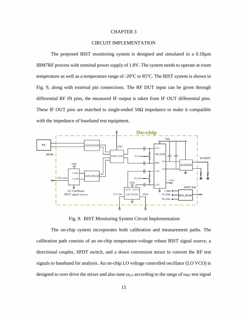
CHAPTER 3
CIRCUIT IMPLEMENTATION
The proposed BIST monitoring system is designed and simulated in a 0.18µm
IBM7RF process with nominal power supply of 1.8V. The system needs to operate at room
temperature as well as a temperature range of -20oC to 85oC. The BIST system is shown in
Fig. 9, along with external pin connections. The RF DUT input can be given through
differential RF IN pins, the measured IF output is taken from IF OUT differential pins.
These IF OUT pins are matched to single-ended 50Ω impedance to make it compatible
with the impedance of baseband test equipment.
Fig. 9. BIST Monitoring System Circuit Implementation
The on-chip system incorporates both calibration and measurement paths. The
calibration path consists of an on-chip temperature-voltage robust BIST signal source, a
directional coupler, SPDT switch, and a down conversion mixer to convert the RF test
signals to baseband for analysis. An on-chip LO voltage controlled oscillator (LO VCO) is
designed to over drive the mixer and also tune ωLO according to the range of ωRF test signal

16
defined by the frequency of the DUT. Two well-matched couplers are used to make equal
gain on both paths as discussed earlier in methodology considerations. It should be noted
that all the components of the system are designed for impedance matching with 50Ω single
ended or in some cases 100Ω differential inputs and outputs. This allows the system to
have maximum power transfer and remain compatible with the standard impedance of the
DUT tested for measurement. The RF signal path is characterized with frequency planning
and link budget analysis on system level before circuit design implementation.
The different BIST system blocks are designed and laid out to achieve a final
integration and a complete on-chip implementation. Each of them are explained in detail
and design tradeoffs are discussed in the following subsections.
3.1 BIST signal source:
The BIST signal source is the critical block for this monitoring system. The
objective of this block is to create an on-chip test signal with a known and robust amplitude
value, which remains unchanged over supply voltage and temperature.
A cross coupled differential LC oscillator topology is selected for signal generation
[24]. Based on the LC tank resonance, the oscillation frequency is created. Since these
components are not ideal and has loss a parallel resistance RP can be assumed.
𝑓𝑂𝑆𝐶 = 1/√(𝐿𝑡𝑎𝑛𝑘𝐶𝑡𝑎𝑛𝑘) (3.1)
This is also called a negative-gm oscillator. The negative resistance looking into the
cross-coupled NMOS pair can be expressed by [25]
𝑅𝑖𝑛 = − 2/𝐺𝑚 (3.2)
If this Rin is less than or equal to parallel resistance RP of the LC core tank, then the
circuit oscillates based on the Barkhausen criterion. Another way to look at it is that to

17
achieve the steady state oscillation the equivalent parallel resistance created by the LC tank
should be balanced with negative resistance created by the active circuit. When this
condition is satisfied, the circuit becomes lossless and generates oscillation. Essentially,
any energy dissipated in RP is compensated for with the energy produced by the active
circuitry.
For a given LC tank, RP and thus Gm are set. In typical submicron CMOS
technologies, an NMOS gives more transconductance per current than the same size PMOS
transistor. As a result, NMOS-based cross couple oscillators are most efficient in terms of
start-up. Hence, for a given current budget and required RP, these implementation result in
a smaller active area and thus less parasitic capacitances.
If the oscillator is biased to work in current regime, where the output swing is within
the available voltage headroom, this swing can be given by [24]
𝑉𝑜𝑢𝑡, 𝑝 = 4
𝜋𝐼𝑆𝑆𝑅𝑃 (3.3)
The peak to peak amplitude of the oscillator output is dependent on the bias current,
shunt resistance, and hence it is sensitive to PVT variations. Constant and robust amplitude
is highly desired in the calibration path, since it is used as a reference to calculate the DUT’s
output amplitude. Performance of the BIST system is influenced by the amplitude of the
reference oscillator’s output. With a small variation of amplitude VCO output, a
proportionate error will be observed at the DUT measurement. To make the amplitude
robust and optimized, we device a feedback mechanism. This method, called automatic
amplitude control is implemented in previous works for optimizing the phase noise of the
LC VCOs [26-27]

18
In this design, the automatic amplitude control scheme is adapted to minimize the
change in output amplitude caused by voltage and temperature variations [28]. The
schematic of the NMOS LC Oscillator with amplitude control loop is shown in the Fig. 10.
It contains three main sub-circuits: LC oscillator, peak detector and comparator. The
amplitude control is performed by the peak detector and comparator blocks.
A source follower based peak detector is used in the control block; this peak
detector senses the peak value of the oscillator output amplitude and creates a DC signal
proportional to the amplitude level. Based on the peak detector output signal, the error
amplifier output varies and in-turn controls the bias current of the LC oscillator. On-chip
bandgap reference voltage [29], which is robust to voltage and temperature (VT) variations,
is used as reference for this amplifier.
Fig. 10. LC Oscillator with Amplitude Control Loop
Vdd
OSC_bias
RFOUTN RFOUTP
Vref
+
-
Vbias

19
In addition to the control bias tail current source, a fixed bias source with a small
portion of current is added and biased externally to provide start-up to the oscillator in case
of initial oscillation problems. The two output buffers are added to facilitate the matching
with the next RF stage. The low pass filter on the output of the error amplifier helps in
filtering out the low frequency noise generated by the amplitude control circuitry
Fig. 11. Output Amplitude Settling of LC Oscillator
Fig.11 shows the differential output of the LC oscillator with amplitude controlled
and settled to a nominal value. The BIST signal source is designed using amplitude control
scheme to make it robust with VT variations. The automatic amplitude control LC
oscillator provides a peak amplitude variation of less than 20mV for a nominal value of
420mVpp at an operating frequency of 2.4GHz, and the output settles down within less than
50ns.
3.2 Directional Coupler:
A directional coupler is designed on-chip using integrated lumped elements to get
high linearity for high power measurement of the PAs. The coupler schematic is shown in
Fig. 12. In this coupler, In+ and In- are the differential inputs, and Cou+ and Cou- are the
differential coupled outputs. The through path outputs and isolated path outputs are
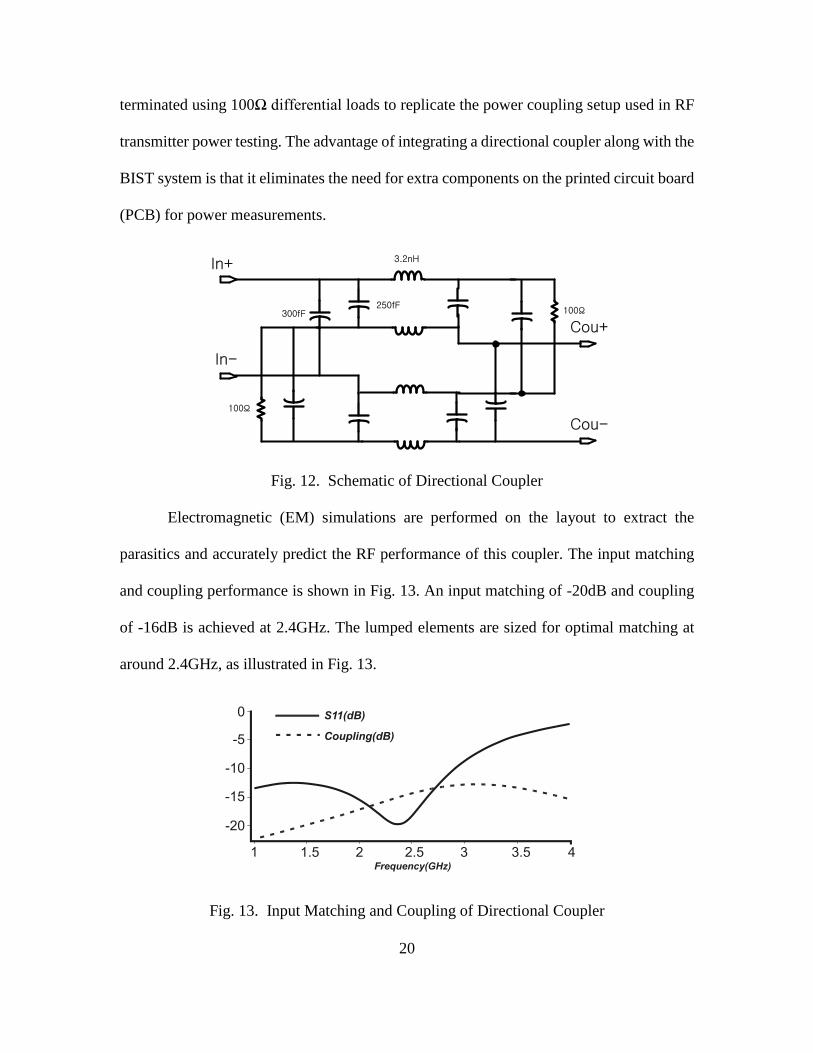
20
terminated using 100Ω differential loads to replicate the power coupling setup used in RF
transmitter power testing. The advantage of integrating a directional coupler along with the
BIST system is that it eliminates the need for extra components on the printed circuit board
(PCB) for power measurements.
In+
In-
Cou+
Cou-
3.2nH
100Ω
100Ω
250fF300fF
Fig. 12. Schematic of Directional Coupler
Electromagnetic (EM) simulations are performed on the layout to extract the
parasitics and accurately predict the RF performance of this coupler. The input matching
and coupling performance is shown in Fig. 13. An input matching of -20dB and coupling
of -16dB is achieved at 2.4GHz. The lumped elements are sized for optimal matching at
around 2.4GHz, as illustrated in Fig. 13.
Fig. 13. Input Matching and Coupling of Directional Coupler

21
3.3 SPDT RF Switch:
A Single Pole Double Throw CMOS RF switch has been used to connect the
coupled signals from the DUT and BIST test signal sources to the input of the Mixer. It is
controlled by two inverted signals Ctrl1 and Ctrl2. Based on Ctrl signal either the DUT
coupled signal or test coupled signal is passed through the switch.
CMOS switches have a single-pin control interface that enables maximum circuit
layout efficiency benefitting our BIST application. This is possible because CMOS allows
the integration of the driver and switch control circuitry with the switches, effectively
reducing the number of control pins [30].
Ctrl 1 Ctrl 2CtrlC
trl 2
Ctrl 2In1+
Out+
Ctrl 1
Ctrl 2
In2+
Ctrl 1
In1-
Out-
Ctrl 1
Ctrl 2
In2-
Ctrl 1
Fig. 14. Schematic of Single Pole Double Throw Switch
The SPDT switch schematic is shown in Fig. 14. N-channel transistors were used
in the design to provide low-on resistance to reduce insertion loss [31]. The circuit consists
of two series/shunt topologies, where the series transistors are the main switching
22
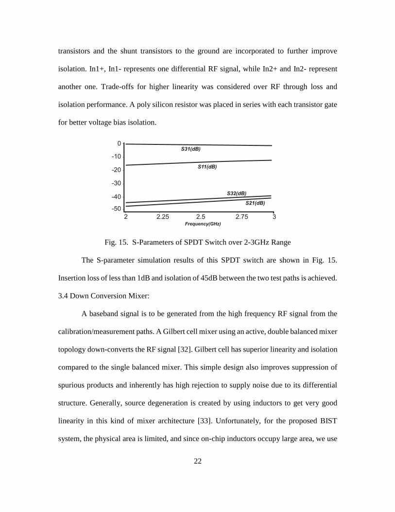
transistors and the shunt transistors to the ground are incorporated to further improve
isolation. In1+, In1- represents one differential RF signal, while In2+ and In2- represent
another one. Trade-offs for higher linearity was considered over RF through loss and
isolation performance. A poly silicon resistor was placed in series with each transistor gate
for better voltage bias isolation.
Fig. 15. S-Parameters of SPDT Switch over 2-3GHz Range
The S-parameter simulation results of this SPDT switch are shown in Fig. 15.
Insertion loss of less than 1dB and isolation of 45dB between the two test paths is achieved.
3.4 Down Conversion Mixer:
A baseband signal is to be generated from the high frequency RF signal from the
calibration/measurement paths. A Gilbert cell mixer using an active, double balanced mixer
topology down-converts the RF signal [32]. Gilbert cell has superior linearity and isolation
compared to the single balanced mixer. This simple design also improves suppression of
spurious products and inherently has high rejection to supply noise due to its differential
structure. Generally, source degeneration is created by using inductors to get very good
linearity in this kind of mixer architecture [33]. Unfortunately, for the proposed BIST
system, the physical area is limited, and since on-chip inductors occupy large area, we use

23
resistive degeneration, RS. Even though this resistors increase mixer noise figure, it is not
a big concern for our application. Moreover the noise is kept small using small sizes for
RS.
Fig. 16. Schematic of Differential Gilbert Cell Mixer
Fig. 17. Linearity of Mixer
The high frequency components of the IF signal are filtered out using capacitors at
both the outputs of the mixer. Also, the buffers are used to match the mixer stage’s load
impedance to the output load of 50Ω on each side. As shown in Fig. 17, the IIP3 of the
IFP IFN
LOP
LONRFP RFN
Rs Rs
RL RL
LOP
Vdd
I_bias

24
mixer is simulated to be 5dBm, which is higher than the coupled RF signal power coming
into the mixer.
3.5 LO VCO:
A varactor based voltage controlled LC oscillator is used to generate LO signals to
over drive the mixer. The schematic of the VCO is shown in Fig. 18. An NMOS based
cross-coupled differential structure is chosen with a tail source to control the bias current
of the core. The VCO output drives the switching inputs of the mixer through buffers. A
symmetric inductor from IBM 7RF technology is used along with tunable varactors to
create an LC tank [34]. The oscillation frequency is given by:
𝑓𝑂𝑆𝐶 = 1/2𝜋√(𝐿𝑠𝑦𝑚(𝐶𝑑 + 𝐶𝑣 + 𝐶𝑝) (3.4)
From Equation (3.4), Lsym is the inductance of the symmetric inductor, Cd is the
parasitic capacitances of transistors and varactors, Cp is the parasitic capacitance due to the
interconnection, and Cv is the capacitance of varactors seen at oscillation nodes. An
external biasing is set to mirror the tail current and can be controlled by an external
potentiometer for flexibility of current values.
Vdd
Ibias
Vtune
LO1 LO2
Fig. 18. Schematic of LO VCO

25
A fine frequency control is achieved using MOS varactors in the LC tank core. As
the oscillation frequency depends on the Cd, it can be tuned using the MOS varactors [35].
Fig. 19. Frequency Tuning Range of LO VCO
The tuning range and KVCO of this oscillator are shown in Fig. 19. The VCO
frequency can be tuned from 2.3GHz to 2.45GHz with KVCO of 85MHz/V. The tuning
voltage of 0.6V is used to get fLO of 2.39GHz for an IF frequency of 10MHz planned for
baseband measurements.
3.6 Chip Integration and Top Level Routing:
The complete BIST monitoring system is integrated and fabricated in a 0.18 µm,
seven metal layer RF CMOS process and occupies a core area of 0.65mm x 2.1mm. A die
photograph for the IC including the pad ring is shown in Fig. 20. The entire die including
ESD pad ring occupies an area of 1.5mm x 3mm. The fabricated chip was packaged in a
24-pin QFN package for testing. As shown earlier in Fig. 9, the two differential RF input
and differential IF output pins are the critical I/O for this chip. The other connected pins
are used for biasing the BIST signal source, mixer and LO VCO. A SPDT Ctrl pin is placed
close to the SW block and used with external signal of either 0 (GND) or 1 (VDD) to

26
control the switching between calibration and measurement paths. The LO VCO frequency
tuning is managed through a tuning pin using an external voltage Vtune.
Fig. 20. Chip Die Microphotograph
Table 2. Area Overhead of the BIST System
Circuit Area (mm2)
Oscillator 0.32
LO VCO 0.137
Mixer 0.122
Switch 0.015
Couplers 0.422
Total Area 1.016
RF transceiver [22-23] 9
%Overhead 11.28%
Table 2 shows the layout area of the different BIST on-chip circuits. As we can see,
the two directional couplers consume a major portion of the area because of the large sizes
of lumped elements. This system introduces approximately 1mm2 area overhead, and this
can be significantly reduced with more layout time and techniques.

27
CHAPTER 4
MEASUREMENT RESULTS
A double sided FR4 PCB board is designed for evaluation and characterization of
the BIST monitoring chip. The PCB with on board components can be seen in Fig. 21. The
24-pin BIST chip is mounted and assembled, along with the potentiometers and DC power
jacks. RF IN and IF OUT pins can be accessed through SMA connectors. A toggle switch
is assembled to control the SPDT Ctrl input, which switches between calibration and
measurement paths as discussed earlier in test methodology.
Fig. 21. Evaluation PCB
Since the extracted or measured APA is the amplitude entering the chip, we calibrate
out board and other losses involved in the connection of the DUT to the BIST chip. So, a
replica path of the RF IN differential path is designed on the PCB for initial calibration of
this path loss.

28
Fig. 22. Hardware Setup for Path Loss Calibration
In this calibration step, as shown in Fig. 23 a vector signal generator (N5182A) is
used to inject power at SMA1 and the output power from SMA2 is measured using a signal
analyzer (N9020A). The loss between the injected power and measured power gives the
estimate of losses of cable, SMA connector and the transmission line on the PCB.
C
S
C
S
T T
SMA2SMA1
Fig. 23. Evaluation Board Path Loss Diagram

29
The two cables have nearly the same loss at a particular frequency of 2.4GHz. C,
S, T represent the losses of cable, SMA connector and on-board RF path, respectively.
Test power – Measured power = Loss of the path = 2(C+S+T) (4.1)
Loss of single ended path = (C+S+T) (4.2)
Multiple measurements of path losses with different injected powers are initially
calibrated out to be further used in the BIST measurements. Different GPath values for
injected power inputs are shown in Table 3 below.
Table 3. GPATH Loss Results
Pin (dBm) Pout (dBm) GPath (dB)
-10 -12.47 -2.47
-5 -7.50 -2.50
0 -2.45 -2.45
5 2.62 -2.48
Since the replica path is designed exactly with the same transmission path length
and SMA connectors similar to RF IN, GPATH values can be assumed as the loss values for
the RF IN path to the input of the BIST chip with good accuracy.
4.1 Testing of BIST Signal Source:
Amplitude controlled BIST signal source is designed to maintain constant and
robust output amplitude over VT variations. This section concentrates on testing the
monitoring system for accuracy of the BIST signal source over VT variations.
This test setup requires three steps. (1) Measurement of output with injected RF
input from external signal generator (2) Calculation of path gain using Equation (2.14) (3)
Switch to connect the BIST signal source to the gain path and extract its amplitude based
30
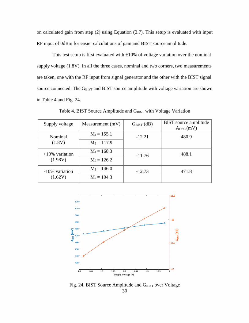
on calculated gain from step (2) using Equation (2.7). This setup is evaluated with input
RF input of 0dBm for easier calculations of gain and BIST source amplitude.
This test setup is first evaluated with ±10% of voltage variation over the nominal
supply voltage (1.8V). In all the three cases, nominal and two corners, two measurements
are taken, one with the RF input from signal generator and the other with the BIST signal
source connected. The GBIST and BIST source amplitude with voltage variation are shown
in Table 4 and Fig. 24.
Table 4. BIST Source Amplitude and GBIST with Voltage Variation
Supply voltage Measurement (mV) GBIST (dB) BIST source amplitude
AOSC (mV)
Nominal
(1.8V)
M1 = 155.1 -12.21 480.9
M2 = 117.9
+10% variation
(1.98V)
M1 = 168.3 -11.76 488.1
M2 = 126.2
-10% variation
(1.62V)
M1 = 146.0 -12.73 471.8
M2 = 104.3
1.6 1.65 1.7 1.75 1.8 1.85 1.9 1.95 2
430
440
450
460
470
480
490
500
510
520
Supply Voltage (V)
AO
SC (
mV
)
-13
-12
GB
IST
(dB
)
-11.5
-12.5
Fig. 24. BIST Source Amplitude and GBIST over Voltage

31
This setup is next evaluated for temperature variation of 27ºC to 85ºC with nominal
measurement at room temperature (27ºC). The GBIST and BIST source amplitude results
with temperature variation are shown in Table 5 and Fig. 25.
Table 5. BIST Source Amplitude and GBIST with Temperature Variation
Temperature Measurement (mV) GBIST (dB) BIST source amplitude
AOSC (mV)
27ºC M1 = 155.1
-12.21 480.9
M2 = 117.9
50ºC M1 = 140.6
-13.06 470.9
M2 = 104.7
85ºC M1 = 126.6
-13.97 460.7
M2 = 92.2
20 30 40 50 60 70 80 90
430
440
450
460
470
480
490
500
510
520
Temperature (oC)
AO
SC (
mV
)
-14
-13
-12
GB
IST
(dB
)
Fig. 25. BIST Source Amplitude and GBIST over Temperature
The experimental results from this test setup are in good agreement with the
expected values from simulations. A maximum deviation of 20mV is observed for the
amplitude of the BIST signal source with temperature variation. As we can see, GBIST
changes with VT variations, but the BIST signal source has maintained its robustness and

32
can be used in calibrating the gain variations in the calibration phase which is discussed in
the next section.
4.2 Calibration Phase:
Since the robustness of BIST source amplitude AOSC over voltage and temperature
variations has been verified, the main test methodolgy is implemented using the presented
hardware setup. During this calibration phase, based on the known AOSC parameter, the
GBIST_CALIBRATION parameter needs to be calibrated. The test measurement setup to run this
calibration phase is shown in Fig. 26. The low frequency IF outputs are measured using an
oscilloscope (DSO9254A). It can be seen that since the BIST test signal generated on-chip
is used as a reference amplitude signal there is no requirement for any power input signal.
Fig. 26. Hardware Setup for Calibration Phase
The SPDT switch is switched into calibration path using SW Ctrl = 0. This makes
the reference RF test signal from on-chip signal source to pass through for further down
conversion to baseband.
[𝑀1_𝐴/𝐴𝑂𝑆𝐶] = 𝐺𝐵𝐼𝑆𝑇_𝐶𝐴𝐿𝐼𝐵𝑅𝐴𝑇𝐼𝑂𝑁 (4.3)

33
Based on equation (4.3), the value for GBIST_CALIBRATION is found. Multiple
measurements for this calibration can improve the accuracy of the GBIST_CALIBRATION value
through averaging. But, the downside of more averaging is an increase in the test time.
This standard trade-off needs to be considered according to the accuracy or test time
requirements.
4.3 Measurement Phase:
The test setup used to characterize the measurement system in this phase is
illustrated in Fig. 27. As seen in the figure the low frequency IF differential outputs are
measured using an oscilloscope (DSO9254A). An Agilent N5182A vector signal generator
is used to feed 2.4GHz RF signal at the input port and replicate the DUT. However, we do
not assume the knowledge of the input signal amplitude.
Fig. 27. Hardware Setup for Measurement Phase
The SPDT switch is controlled using SW Ctrl = 1 to allow the RF DUT input signal
to pass for down conversion at the mixer. So, once the GBIST is calibrated for different
corners, the DUT signal amplitude can be extracted by multiple equations given earlier in

34
the test methodology section. While taking these measurements, 20dB range span for the
DUT power from -15dBm to 5dBm is chosen based on the linearity of the blocks along the
measurement path.
𝑀2_𝐴 = 𝐴𝑃𝐴𝐺𝐵𝐼𝑆𝑇_𝑀𝐸𝐴𝑆𝑈𝑅𝐸𝑀𝐸𝑁𝑇 (4.4)
(𝑀2_𝐴/𝑀1_𝐴) ∗ 𝐴𝑂𝑆𝐶 = 𝐴𝑃𝐴 (4.5)
Based on multiple M2 and M1 measurements with calibration APA can be computed
with good accuracy. The injected signal power from the DUT input is attenuated by losses
of the cable and RF transmission path on the board connecting the RF input of the chip.
The calibrated losses from measurements using a replica transmission path on the board,
as explained earlier, are used in this phase along with GBIST_CALIBRATION to extract DUT
signal amplitude.
The comparison of the injected power from the DUT and the extracted values from
the measured BIST are shown in Table 6. The first case represents the measurements at
nominal corner, while second and third are computed at voltage and temperature corners
respectively. The fourth case is computed at the extreme voltage and temperature corner to
verify the accuracy. Three injected power values of -5dBm, 0dBm and 5dBm are chosen
for quantification in the above table. The power measurement comparison with the injected
values at different corners is shown by the plots in further Fig. 28-29.

35
Table 6. Calculated vs Measured Power Comparison
APA calculated with RF
IN (dBm)
APA measured using
BIST (dBm)
Error
(dB)
VDD = 1.8 V
Temp = 27oC
-5 -4.92 0.08
0 0.05 0.05
5 4.96 0.04
VDD = 1.8 V
Temp = 85oC
-5 -5.35 0.35
0 -0.25 0.25
5 4.78 0.22
VDD = 1.98
V
Temp = 27oC
-5 -4.67 0.33
0 0.22 0.22
5 5.15 0.15
VDD = 1.98
V
Temp = 85oC
-5 -5.36 0.36
0 0.27 0.27
5 4.82 0.18
Fig. 28. Injected vs BIST Computed Power at Nominal and Voltage Corner
-15 -10 -5 0 5-15
-10
-5
0
5
Injected Power [dBm]
BIS
T C
om
pute
d P
ow
er
[dB
m]
-15 -10 -5 0 5-15
-10
-5
0
5
Injected Power [dBm]
BIS
T C
om
pute
d P
ow
er
[dB
m]

36
Fig. 29. Injected vs BIST Computed Power at Temperature and VT Corner
As we can see from four cases and plots, the error at the corners increases because
the initial calibrated source amplitude has corner variation. This causes an error in the
computation of the DUT output. This error or offset from the ideal computed power is
directly dependent on the variations caused by the BIST signal source, PCB path loss
measurements, GBIST calibration, and any mismatch between the gains of calibration and
measurement paths. The measured results verify that the on-chip BIST system accurately
measures the DUT output amplitude over supply voltage and temperature variations.
-15 -10 -5 0 5-15
-10
-5
0
5
Injected Power [dBm]
BIS
T C
om
pute
d P
ow
er
[dB
m]
-15 -10 -5 0 5-15
-10
-5
0
5
Injected Power [dBm]
BIS
T C
om
pute
d P
ow
er
[dB
m]

37
CHAPTER 5
CONCLUSION AND FUTURE WORK
A BIST solution for in-field monitoring of the output power and gain for an RF
power amplifier DUT is proposed. This system is capable of detecting the true power
delivered to the load with accuracy of 0.35dB over a 20dB power dynamic range. The
proposed system is targeted for ISM (2.4GHz) applications and is well suited for
integration with RF SoCs.
An on-chip RF test signal generator robust over voltage and temperature variations
is designed and calibrates the entire BIST system before actual DUT monitoring. By using
some additional circuitry like an RF switch and down conversion mixer, the BIST module
is able to convert the RF system response to a simpler form at baseband for low-overhead
analysis and signal processing. Simulation and hardware measurements show that the
output power and gain measurement at 2.4GHz can be done without any computational
complexity. The entire system is implemented on-chip, paving the way for on-chip
characterization and calibration.
RF transmitters are highly complex and there are more parameters that should be
considered for BIST monitoring, as they affect the performance of the entire RF system.
Thus, the proposed approach can be further expanded to monitor other specifications such
as linearity and supply modulation in the power amplifier DUT.

38
REFERENCES
[1] Ericsson Mobility report: On the pulse on the networked society
http://www.ericsson.com/res/docs/2015/mobility-report/ericsson-mobility-report-nov-
2015.pdf
[2] Liu, Yidong, and Jiann-Shiun Yuan. "CMOS RF power amplifier variability and
reliability resilient biasing design and analysis." Electron Devices, IEEE Transactions
on 58.2 (2011): 540-546.
[3] Yuan, J. S., and E. Kritchanchai. "Power amplifier resilient design for process, voltage,
and temperature variations." Microelectronics Reliability 53.6 (2013): 856-860.
[4] Presti, Calogero D., et al. "A 25 dBm digitally modulated CMOS power amplifier for
WCDMA/EDGE/OFDM with adaptive digital predistortion and efficient power
control." Solid-State Circuits, IEEE Journal of 44.7 (2009): 1883-1896.
[5] Boumaiza, Slim, et al. "Adaptive digital/RF predistortion using a nonuniform LUT
indexing function with built-in dependence on the amplifier nonlinearity."Microwave
Theory and Techniques, IEEE Transactions on 52.12 (2004): 2670-2677.
[6] Wen-Jie, Mao, Ran Li-Xing, and Chen Kang-Shen. "Adaptive predistortion for RF
power amplifier based on new look-up table indexing method." Microwave and Millimeter
Wave Technology, 2002. Proceedings. ICMMT 2002. 2002 3rd International Conference
on. IEEE, 2002.
[7] Muhonen, Kathleen J., Mohsen Kavehrad, and Rajeev Krishnamoorthy. "Look-up table
techniques for adaptive digital predistortion: a development and comparison." Vehicular
Technology, IEEE Transactions on 49.5 (2000): 1995-2002.
[8] Kyung Ai Lee, Dong Ho Lee, “A InGaP/GaAs HBT WLAN Power Amplifier with
Power Detector” 34" European Microwave Conference - Amsterdam, 2004
[9] Lei, Feiran, et al. "A RF/DC current-mode detector for BiST and digital calibration of
current-driven mixers." Electronics, Circuits and Systems (ICECS), 2012 19th IEEE
International Conference on. IEEE, 2012.
[10] Ossi PollSinen, Esko Jiirvinen, “Integrated Power Measurement Circuit for RF Power
Amplifiers” Radio and Wireless conference 2000. RAWCON 2000. 2000 IEEE.
[11] J.-Y. Ryu, B. Kim, and I. Sylla, “A new low-cost RF built-in selftest measurement
for system-on-chip transceivers,” IEEE Trans. Instrum. Meas., vol. 55, no. 2, pp. 381–388, Apr. 2006.

39
[12] D. Han and A. Chatterjee, “Robust built-in test of RF ICs using envelope detectors,
” in Proc. 4th Asian Test Symp., Dec. 2005, pp. 2–7.
[13] M. Barragan, R. Fiorelli, D. Vaquez, A. Rueda, and J. Huertas, “Lowcost signature
test of RF blocks based on envelope response analysis,” in Proc. IEEE Eur. Test Symp.
(ETS), May 2010, pp. 55–60.
[14] M. Barragan, R. Fiorelli, D. Vazquez, A. Rueda, and J. Huertas, “On-chip
characterisation of RF systems based on envelope response analysis,” Electron. Lett., vol.
46, pp. 36–38, Jul. 2010.
[15] D. Han, S. Bhattacharya, and A. Chatterjee, “Low-cost parametric test and diagnosis
of RF systems using multi-tone response envelope detection,” Comput. Digital Tech., vol.
1, pp. 170–179, May 2007.
[16] M. Negreiros, L. Carro, and A. A. Susin, “Reducing test time using an enhanced RF
loopback,” J. Electron. Testing, vol. 23, no. 6, pp. 613–623, 2007.
[17] J. Dabrowski and J. Bayon, “Mixed loopback BIST for RF digital transceivers,” in
Proc. IEEE Defect and Fault Tolerance in VLSI Systems (DFT 2004), Oct. 2004, pp. 220
– 228.
[18] A. Nassery and S. Ozev, “An analytical technique for characterization of transceiver
IQ imbalances in the loop-back mode,” in Design, Automation Test in Europe (DATE),
2012, pp. 1084–1089.
[19] A. Haldes, S. Bhattacharya, G. Srinivasan, and A. Chaterjee, “A system-level
alternate test approach for specification test of RF transceivers in loopback mode,” in
Proc. Int. Conf. on VLSI Design (VLSID’05), 2005, pp. 132–137.
[20] A. Nassery, O.E. Erol, S. Ozev, and M. Verhelst, “Test Signal Development and
Analysis for OFDM Systems RF Front-End Parameter Extraction,” IEEE Transactions
on Computer-Aided Design of Integrated Circuits and Systems,vol.31, no.6, pp.958-967,
June 2012.
[21] E.S. Erdogan and S. Ozev, “Detailed Characterization of Transceiver Parameters
Through Loop-Back-Based BiST,” IEEE Transactions on Very Large Scale Integration
(VLSI) Systems,vol.18, no.6, pp.901-911, June 2010.
[22] Komurasaki, H.; Sano, T.; Heima, T.; Yamamoto, Kazuya; Wakada, H.; Yasui, I.;
Ono, Masayoshi; Miwa, T.; Sato, H.; Miki, T.; Kato, N., "A 1.8-V operation RF CMOS
40
transceiver for 2.4- GHz-band GFSK applications," Solid-State Circuits, IEEE Journal of ,
vol.38, no.5, pp.817,825, May 2003.
[23] S. Lee; Y. Seo; B. Kim; S. Choi; C. Kim, "An IEEE 802.15.4g sun compliant MR-
OFDM RF CMOS transceiver for smart grid and CES," Consumer Electronics, IEEE
Transactions on , vol.59, no.3, pp.460,466, August 2013.
[24] B. Razavi, RF Microelectronics, Prentice-Hall, 1998.
[25] B. Razavi, Design of Analog CMOS Integrated Circuits, McGraw-Hill, 2001.
[26] Zanchi, A.; Samori, C.; Levantino, S.; Lacaita, A.L, "A 2-V 2.5-GHz - 104-dBc/Hz at
100kHz fully integrated VCO with Wide-Band LowNoise Automatic Amplitude Control
Loop," IEEE J. Solid-State Circuits, vol.36, Issue 4, pp. 611-619, 2001.
[27] Rogers, J.W.M.; Rahn, D.; Plett, C, "A Study of Digital and Analog Automatic-
Amplitude Control Circuitry for Voltage-Controlled Oscillators," IEEE J. Solid-State
Circuits, vol.38, Issue 2, pp. 352-356, 2003.
[28] Zhang, Yuxiang, et al. "Novel Hybrid Type Automatic Amplitude Control Loop
VCO." Electronics, Communications and Control (ICECC), 2011 International Conference
on. IEEE, 2011.
[29] Banba, Hironori, et al. "A CMOS bandgap reference circuit with sub-1-V
operation." Solid-State Circuits, IEEE Journal of 34.5 (1999): 670-674.
[30] X. J. Li and Y. P. Zhang, “Flipping the CMOS switch,” IEEE Microw. Mag., vol. 11,
no. 1, pp. 86–96, 2010.
[31] Huang, Feng-Jung. "A 2.4-GHz single-pole double-throw T/R switch with 0.8-dB
insertion loss implemented in a CMOS process." Solid-State Circuits Conference, 2001.
ESSCIRC 2001. Proceedings of the 27th European. IEEE, 2001.
[32] Barrie Gilbert,, "A precise four-quadrant multiplier with subnanosecond response,"
in Solid-State Circuits, IEEE Journal of , vol.3, no.4, pp.365-373, Dec. 1968.
[33] Park, Jinsung, et al. "Design and analysis of low flicker-noise CMOS mixers for direct-
conversion receivers." Microwave Theory and Techniques, IEEE Transactions on 54.12
(2006): 4372-4380.
[34] Choi, Tae-young, et al. "A low phase noise 10 GHz VCO in 0. 18/spl mu/m CMOS
process." Wireless Technology, 2005. The European Conference on. IEEE, 2005.
[35] Lee, Han-il, et al. "An extremely low power 2 GHz CMOS LC VCO for wireless
communication applications." Wireless Technology, 2005. The European Conference on.
IEEE, 2005.