in - cornell university tunneling into a nanotube ... with advances in technology over the past few...
TRANSCRIPT

1
Carbon Nanotubes: Electrons in One Dimension
by
Marc William Bockrath
B.S. (Massachusetts Institute of Technology) 1993
A dissertation submitted in partial satisfaction of the requirements
for the degreeof
Doctor of Philosophyin
Physics
In the
GRADUATE DIVISION
of the
UNIVERSITY OF CALIFORNIA, BERKELEY
Committee in charge:
Professor Paul McEuen, ChairProfessor Steven Louie
Professor Gabor Somorjai
Fall 1999

2
Abstract
Carbon Nanotubes: Electrons in One Dimension
by
Marc William Bockrath
Doctor of Philosophy in Physics
University of California, Berkeley
Professor Paul McEuen, Chair
The work presented in this thesis will discuss transport measurements on
individual single-walled nanotubes (SWNTs) and SWNT bundles. SWNTs, which are
essentially rolled-up sheets of graphite, are either one-dimensional (1D) metals or 1D
semiconductors depending on how they are rolled-up. Measurements on both metallic
and semiconducting SWNTs will be presented.
Chapter 1 will present an introductory overview to the thesis, discussing prior
related experimental work and introducing basic concepts that are used in subsequent
chapters. Chapter 2 discusses the experimental methods we have used to study
transport in SWNTs.
Chapters 3 and 4 discuss low temperature measurements of metallic SWNTs.
Chapter 3 will discuss the low temperature behavior of the conductance of a SWNT
bundle, or rope, that shows quantum mechanical effects resulting from the finite size of
the sample. Chapter 4 will discuss how these finite size effects can be used to
experimentally study the quantum level structure in metallic nanotubes and the effects
of an applied magnetic field.

3
In chapters 5 and 6, we discuss transport measurements of semiconducting
SWNTs. In chapter 5, we show that semiconducting SWNTs can be doped with
potassium. Chapter 6 presents experiment and theory that indicate that the elastic mean
free path in metallic tubes is far longer than in semiconducting tubes.
Chapters 7 and 8 address the effects of electron-electron (e-e) interactions on the
transport properties of metallic SWNTs. Chapter 7 discusses some theoretical aspects
of 1D wires when e-e interactions are taken account, giving a simplified picture of the
Luttinger-liquid state expected for a 1D system of interacting electrons. Finally,
chapter 8 will discuss measurements on metallic samples with extremely long mean
free paths. These experiments show evidence of this Luttinger-liquid behavior, in
which the electron-electron interactions lead to a qualitatively different ground state
than what would be expected with Fermi-liquid theory.

4
To my parents

5
Acknowledgments
The work of this thesis has been largely a collaborative effort. While there are
many people to thank for their contributions, I would first like to thank my advisor Paul
McEuen. His insight into physics (and everything else!) has been a constant source of
inspiration. I am grateful that I have had the opportunity to learn from him.
I also owe a large debt of gratitude to Dave Cobden. His hard work and
guidance were crucial in ensuring the success of these experiments. If not for his
efforts, this thesis would have been much shorter.
The potassium doping experiments would not have happened if not for Jim
Hone. Thanks to his efforts, we were able to get data in record time. I would also like to
thank Jia Lu for providing nanotube samples that permitted clear observations of
Luttinger liquid behavior.
Overall, our efforts have been accelerated by the contributions of Steve Louie,
Young-Gui Yoon, and Leon Balents, who provided theoretical support. Of course,
research on nanotubes would not be possible without nanotubes -- Nasreen Chopra,
Alex Zettl, Andreas Thess, Andrew Rinzler, and Richard Smalley have provided us
with the invaluable material as well as helpful discussions.
Finally, I would also like to thank my co-workers for making the lab an exciting
and stimulating place to work. In particular, I would like to thank Hongkun Park for his
guidance (scientific and otherwise), encouragement, and rides up the hill.
Outside of the lab, I am grateful that I have had the support of my family and
friends for these years. Also, I can not thank Debbie enough for her support and
encouragement. I will always cherish our time together here.

6
Table of Contents
Chapter 1: Carbon Nanotubes: Electrons in One Dimension ...........................................7
1.1 Introduction .............................................................................................................7
1.2 Brief History of Carbon Nanotubes.......................................................................10
1.3 Nanotube Band structure .......................................................................................12
1.4 Experimental Work ...............................................................................................16
Chapter 2: Experimental Techniques..............................................................................18
2.1 Sample Preparation................................................................................................18
2.2 Low Temperature Electrical Measurements..........................................................25
2.3 Basic Observations ................................................................................................28
Chapter 3: Single-Electron Transport in Ropes of Carbon Nanotubes...........................32
Chapter 4: Spin Splitting and Even-Odd Effects in Carbon Nanotubes.........................48
Chapter 5: Chemical Doping of Individual Semiconducting Carbon Nanotube Ropes .63
Chapter 6: Disorder, pseudospins, and backscattering in carbon nanotubes ..................73
Chapter 7: Electrons in One Dimension: Theory............................................................88
7.1 Introduction ...........................................................................................................88
7.2 Low-energy Lagrangian for a single spinless mode..............................................89
7.3 Phenomenological Model for Nanotubes ..............................................................94
7.4 Tunneling Density of States and the Semiclassical Approximation .....................99
7.5 Tunneling into a Nanotube ..................................................................................101
7.6 Limit of Many Modes and Connection to Coulomb Blockade Model................108
7.7 Summary..............................................................................................................112
Chapter 8: Luttinger Liquid Behavior in Carbon Nanotubes .......................................114
Chapter 9: Summary .....................................................................................................128
7
Chapter 1
Carbon Nanotubes: Electrons in One Dimension
1.1 Introduction
The dimensionality of a system has a profound influence on its physical
behavior. With advances in technology over the past few decades (e.g. molecular beam
epitaxy), it has become possible to fabricate and study reduced-dimensional systems in
which electrons are strongly confined in one or more dimensions. The study of
reduced-dimensional systems has yielded many important new results. This is evident
from Fig. 1-1, which shows a table of the properties of systems with different
dimensionalities. As can be seen from the table, much of the basic physics of electrons
in any dimension can be understood in terms of non-interacting electrons in a perfect
crystal. For example, non-interacting electrons models can explain why bulk Si is a
semiconductor or why two-dimensional (2-D) graphene is a semi-metal.
However, many striking phenomena require models that go beyond the above
simple picture. When considering such models the dimension of the system plays an
important role. For example, in three dimensions (3-D) it is possible for electrons to
remain delocalized even in the presence of disorder, unlike in one-dimensional (1-D)
systems. The dimensionality is no less important in determining the effects of electron-
electron interactions. For a 3-D electron system, unless the interactions are very strong,
the low energy excitations from the ground state behave

8
Interacting Electrons in Solids
NoninteractingPhysics
Include CoulombInteractions
Include Disorder/Lattice Coupling
Band StructureMetals, Insulators
Fermi LiquidMott Insulator(strong interactions)
'
'
'
SuperconductivityAnderson localization.(strong disorder)
2D SubbandsQuantum HallEffect
Fermi liquidFQHE - anyons, skyrmions, etc.
Localization
1D SubbandsConductance quantization
Luttinger LiquidCharge densitywaves, etc.Localization
quantum wells, layered compounds, etc.
lithographically patterned wires, polymers, nanotubes
bulk crytalline solids
Figure 1-1: Electronic systems in varying dimensions. While the non-interacting electron picture explains many of the basic features, many phenomena require including the effects Coulomb interactions, particularly in reduced dimensions.
Figure 1

9
essentially like weakly interacting electrons. This is the well-known Fermi-liquid
behavior; electron-electron interactions do not qualitatively change the picture given by
the independent electron model.
Electrons in 2-D at low magnetic fields are also well described by Fermi-liquid
theory. This has been demonstrated by a wealth of experiments on 2-D electron gasses
in GaAs heterojunctions. When a magnetic field is applied, the single-particle states
are Landau levels, which are then filled with electrons up to the Fermi level. The
number of filled Landau levels at a given magnetic field is referred to as the filling
factor ν. When ν is an integer greater than one, the electrons behave like a Fermi
liquid, as in the integer quantum Hall effect (IQHE). However, at high magnetic fields
when only one Landau level is partially filled, the fractional quantum Hall effect is
observed. Unlike the IQHE, understanding the FQHE requires the inclusion of
electron-electron interactions. Coulomb interactions break the degeneracy of the lowest
Landau level leading to a unique ground state and a gap for excitations. These
excitations can be very different from the bare electrons, having for example fractional
charge. Unlike a 3-D electron system, a 2-D electron system is qualitatively altered by
the effects of electron-electron interactions.
The study of 1-D electron systems based on e.g., semiconductor wires or
constrictions has also yielded important results. Most of these results, such as
conductance quantization, have been explained in terms of non-interacting electrons.
Unlike in 2-D and 3-D, however, the question of what role e-e interactions play in real
1-D systems has been difficult to address, because of the difficulty in obtaining long,
relatively disorder-free 1-D wires. Nevertheless, the prediction of dramatic effects in 1-

10
D due to e-e correlations has motivated a lengthy search for a good experimental
realization of a 1-D system. At last, single-walled carbon nanotubes (SWNTs) have
emerged as a material that promises to overcome these difficulties and provide a model
system for the study of electrons in 1-D.
1.2 Brief History of Carbon Nanotubes
The history of SWNTs begins with the discovery of multi-walled carbon
nanotubes (MWNTs.) MWNTs were first observed by transmission electron
microscopy (TEM) in carbon-arc soot by Iijima in 1991 [1]. These micron-long
nanotubes consisted of two or more concentric shells and range in outer diameter from
~2-20 nm (see Fig. 1-2A-B). Soon after, techniques were developed to increase the
yield of nanotube material[2]. Approximately two years after the discovery of
MWNTs, single-walled nanotubes (SWNTs) consisting of only a single shell of carbon
atoms were discovered independently by Iijima and by Bethune[3, 4]. In contrast to
MWNTs, the typical diameter of these SWNTs was ~ 1 nm. Later work enabled the
bulk production of ~1 nm diameter SWNTs[5]. Figure 1-2C shows an image of an
isolated SWNT. The bulk production of these nanotubes has led to a vast array of
experiments exploring their chemical, mechanical, and electrical properties. Here we
will concentrate on the electrical properties.

11
A B100 nm 10 nm
Figure 1-2: A) TEM images of multi-walled nanotubes. Image is a few hundrednanometers by few hundred nanmeters. B) High resolution TEM image of Multi-walled nanotubes showing the concentric walls of the two nanotubes and hollow core.C) TEM image of an individual 1.4 nm diameter single-walled nanotube.
C
Figure 2

12
1.3 Nanotube Band structure
A SWNT is essentially a single 2-D layer of graphite (a graphene sheet) rolled
into a tube. Graphene is an sp2 bonded network of carbon atoms arranged in a
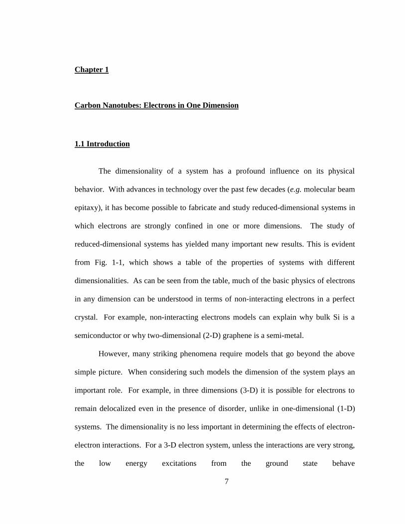
hexagonal lattice with two atoms per unit cell. This is shown in Fig. 1-3A, which
depicts the honeycomb lattice in which a carbon atom is located at each vertex. Figure
1-3A also shows the primitive lattice vectors a1 and a2, as well as the lattice constant a.
A nanotube of a particular radius and chirality may be specified by choosing a “roll-up”
vector that maps two given hexagons in the lattice on top of each other. The blue
arrows in Fig. 1-3A show an example of this for the two hexagons shown in gray.
Since any vector connecting two hexagons in the lattice is a Bravais lattice vector, it is
a linear combination of the primitive vectors with integer weight. Thus, a given
nanotube is associated with two indices that specify these integers. The nanotube
formed by identifying the two gray hexagons in Fig. 1-3A would thus be a (3,1)
nanotube. Note that this indexing scheme is one of convention as the choice of
primitive lattice vectors is not unique. However, this scheme appears to be the most
commonly used in the literature. Figure 1-3B shows how a (10,10) nanotube may be
rolled up from graphene.
For a very large radius tube, one might expect that the properties of the tube are
very similar to that of graphene. It has been found that even for very small diameter
tubes (~1 nm) that the basic electronic properties of nanotubes may be deduced from
the band structure of graphene[6]. Figure 1-4 shows this band structure in the first
Brillouin zone. Since there are two atoms per unit cell, the lower band is completely
13
a1 a2
a
x
y
A
B
Figure 1-3: A) Lattice parameters for graphene: a1 and a2 are the Bravais lattice vectors, a = .243 nm is the lattice constant, and the blue arrows show how a (3,1) nanotube may be formed by rolling the hexagons shown in gray on top of each other. B) A (10,10) nanotube rolled up from graphene

14
-2
-1
0
1
2
3
2π/a0
ky
-2π/a0
kx
2π/a0
Ene
rgy
(Arb
. uni
ts)
Kx
Ky
(5,5) "Armchair" 1D metal (6,4) chiral (insulator)
(4π/3a,0)
Figure 1-4: Graphene band structure. The conduction and valence bands touch at the six Fermi points indicated. Because there are two electrons per unit cell, the valence band is filled and the conduction band is empty. Graphene is thus a zero gap semiconductor, or semimetal.
Figure 1-5: In a nanotube, the periodic boundary conditions quantize the allowed k-values. The nanotube may be insulating or metallic depending on whether the Fermi points coincide with an allowed k-value.

15
filled. The Fermi surface then consists of two inequivalent Fermi points at the opposite
corners of the hexagonal Brillouin zone where the conduction band (CB) and valence
band (VB) touch. The six points where the CB and VB touch shown in Fig. 1-4 are
obtained by translating the two inequivalent points by reciprocal lattice vectors.
In the simplest possible model, the band structure of nanotubes can be derived
directly from the band structure of graphene. This is accomplished by imposing strictly
periodic boundary conditions for translations by the roll-up vector that defines the
nanotube. The allowed k values are then quantized in the direction perpendicular to the
roll-up vector R: kìR = 2πn, where n is an integer. Thus, the band structure of a
nanotube consists of 1-D subbands. For a 1 nm diameter tube the subband splitting is
expected to be on the order of one eV[7], and therefore nanotubes are expected to be
truly 1-D materials. Figure 1-5 depicts these allowed k values for a (5,5) tube and a
(6,4) tube. The nanotube will have a band gap unless the lines of allowed k pass though
the two gapless points. Thus, the (5,5) tube is metallic while the (6,4) tube is
semiconducting, despite the fact that their radii are identical to within less than 1%. In
general, an (n,m) nanotube will have a band gap unless n-m = 3p, where p is an
integer[6-8]. This behavior may also be derived within the context of a low-energy
effective theory[9]. Effects due to curvature result in corrections to this picture. For
example, some tubes that the above model would predict to be metallic may actually
develop a small band gap. However, since these effects have not been observed
experimentally, we will not discuss them here, but refer to the literature (see e.g. [9-
11].)

16
1.4 Experimental Work
STM experiments on individual ~1 nm SWNTs have been able to provide
conclusive evidence for the above theoretical picture[12, 13]. In these experiments,
both the atomic structure and the tunneling spectra for a variety of nanotubes could be
simultaneously measured. The picture given above was found to describe the
experimental results quite well. Depending on the chirality of the nanotube, they were
either metallic or had a band gap of ~0.6 eV. Furthermore, Van Hove singularities in
the density of states were observed at the band edges arising from the one-
dimensionality of the nanotubes. In addition to the STM work, resonant Raman
scattering[14] and transport experiments (for review see e.g. [15]) have also supported
this picture.
A number of these transport experiments will be discussed in the remainder of
this thesis. Some of the chapters describing these experiments have appeared
previously as publications. Specifically, Chapter 3 has been published as Science 275
1922 (1997), Chapter 4 as Phys. Rev. Lett. 81 681 (1998), and Chapter 8 as Nature 397
598 (1999). Other chapters have been submitted for publication but have not yet
appeared. Chapter 5 has been submitted to Applied Physics Letters, and Chapter 6 has
been submitted to Physical Review Letters

17
References
1 S. Iijima, Nature 354, 56 (1991).
2 T. W. Ebbesen and P. M. Ajayan, Nature 358, 220 (1992).
3 S. Iijima and T. Ichihashi, Nature 363, 603 (1993).
4 D. S. Bethune, C. H. Kiang, M. S. deVries, et al., Nature 363, 605 (1993).
5 A. Thess, R. Lee, P. Nikolaev, et al., Science 273, 483 (1996).
6 R. Saito, M. Fujita, G. Dresselhaus, et al., Applied Physics Letters 60, 2204
(1992).
7 N. Hamada, S. Sawada, and A. Oshiyama, Physical Review Letters 68, 1579
(1992).
8 J. W. Mintmire, D. H. Robertson, and C. T. White, Journal of the Physics and
Chemistry of Solids 54, 1835 (1993).
9 C. L. Kane and E. J. Mele, Physical Review Letters 78, 1932 (1997).
10 X. Blase, L. X. Benedict, E. L. Shirley, et al., Physical Review Letters 72, 1878
(1994).
11 L. Balents and M. P. A. Fisher, Physical Review B 55, R11973 (1997).
12 J. W. G. Wildoer, L. C. Venema, A. G. Rinzler, et al., Nature 391, 59 (1998).
13 T. W. Odom, H. Jin-Lin, P. Kim, et al., Nature 391, 62 (1998).
14 A. M. Rao, E. Richter, S. Bandow, et al., Science 275, 187 (1997).
15 C. Dekker, Physics Today 52, 22 (1999).
18
Chapter 2
Experimental Techniques
2.1 Sample Preparation
As discussed in the introduction, SWNTs represent a ready-made 1-D electron
system. Thus, all that is required to study the electrical properties of electrons in 1-D is
to connect these nanotubes to external wires. This section will describe how we attach
leads to individual nanotubes or nanotube bundles and make electrical measurements.
We begin with the raw “felt” material, which is shown in Figure 2-1A. We
obtain this material from Professor Richard Smalley and co-workers at Rice University,
where it is made by laser vaporizing carbon along with small amounts of Co and Ni,
which act as a catalyst. Closer inspection with a scanning electron microscope (SEM)
such as shown in Fig. 2-1B reveals that the felt material consists of very long, tangled
strands. These strands are bundles of SWNTs as shown in cross section in Fig. 2-1C.
They consist of 2D hexagonally packed SWNTs of a nearly monodisperse diameter ~1
nm. An isolated individual SWNT is shown in Fig. 2-1D. In order to make electrical
measurements of single nanotubes or few-nanometer bundles, the individual nanotubes
or bundles must first be isolated from the felt.
To accomplish this, the raw felt material shown in Fig. 2-1A is placed in a
liquid and exposed to ultrasound. The ultrasound produces microscopic bubbles in the
liquid.

19
QP
Figure 2-1: Single walled nanotube material shown at various levels of magnification. A) Nanotube material as it appears on a macroscopic scale. B) At the lowest level of magnification, the material appears as a tangled mass of rope-like strands. (Image from R. E. Smalley.) C) Higher magnification reveals bundles of SWNTs arranged in a hexagonal 2D lattice. (Image from R. E. Smalley.) D) The highest level of magnification shows a side view of a single 1.4 diameter SWNT. (Image from Nasreen Chopra.)
A) B)
C)
D)
20
When these bubbles collapse, the resulting shock waves serve to cut the ropes and
disperse them in the solvent. The diameter of the bundles, the prevalence of single
nanotubes, and the degree to which they are untangled by this procedure depends
critically on precisely which solvent is used. It has been found that 1,2 Dichloroethane
(DCE) is an excellent solvent in this regard. Ultrasounding the felt material in DCE
results in a suspension of nanotubes and bundles with a spectrum of lengths ranging
from < 1 µm to ~ 10 µm, and diameters in the 1-10 nm range. Presently, it is not
understood why DCE works so well. However, the attractive forces between suspended
particles in a liquid depends on many physical properties of the liquid, such as the
dielectric constant, the surface energies of the solvent and solute, etc. Thus, it is not
surprising that different liquids will have different levels of effectiveness at suspending
nanotubes and preventing them from coalescing.
Once the nanotubes are suspended in DCE, they can be deposited on a surface
by placing a drop of the suspension on a substrate. It is found that nanotubes suspended
in DCE will readily adhere to SiO2 by Van der Waals forces. After a few seconds and
before the DCE dries, the suspension is rinsed away with 2-propanol (IPA). This results
in a relatively uniform coverage of nanotubes on the surface. Once the IPA is blown
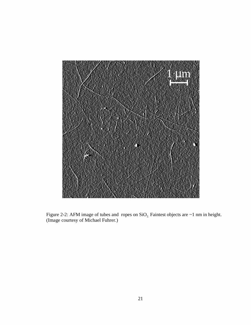
dry, the tubes remain immobilized on the surface. Figure 2-2 shows an atomic force
microscope (AFM) image of silicon dioxide with tubes deposited in this way.
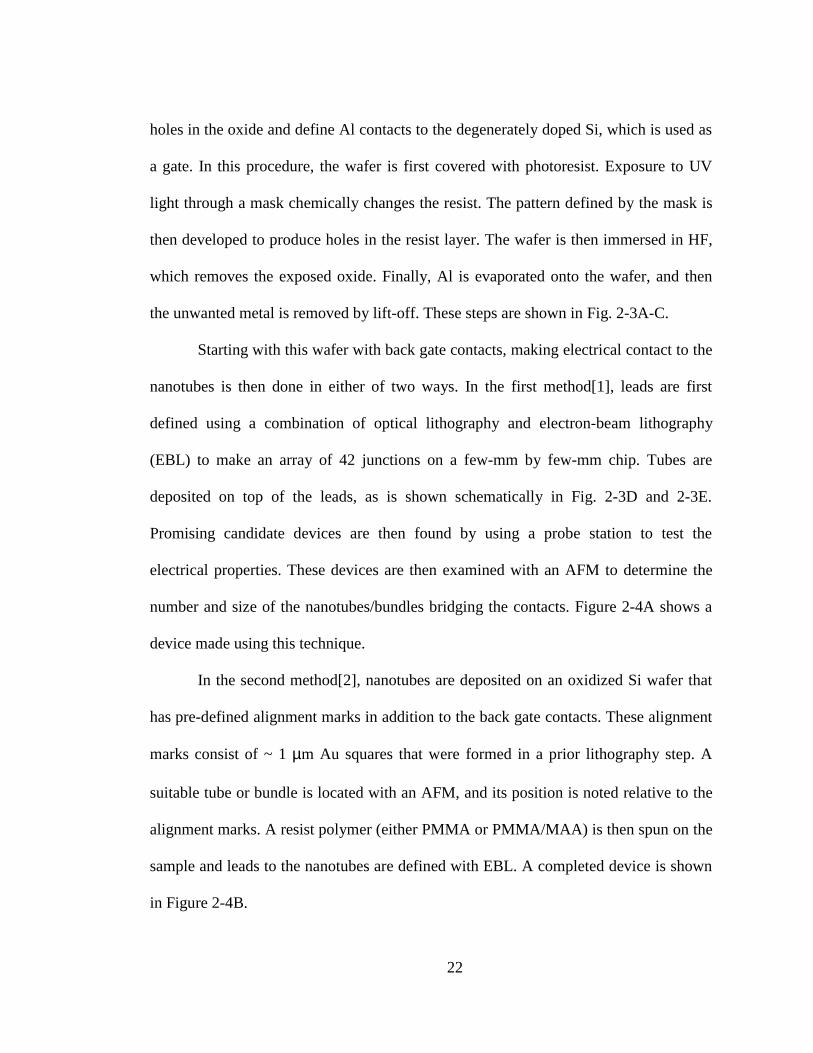
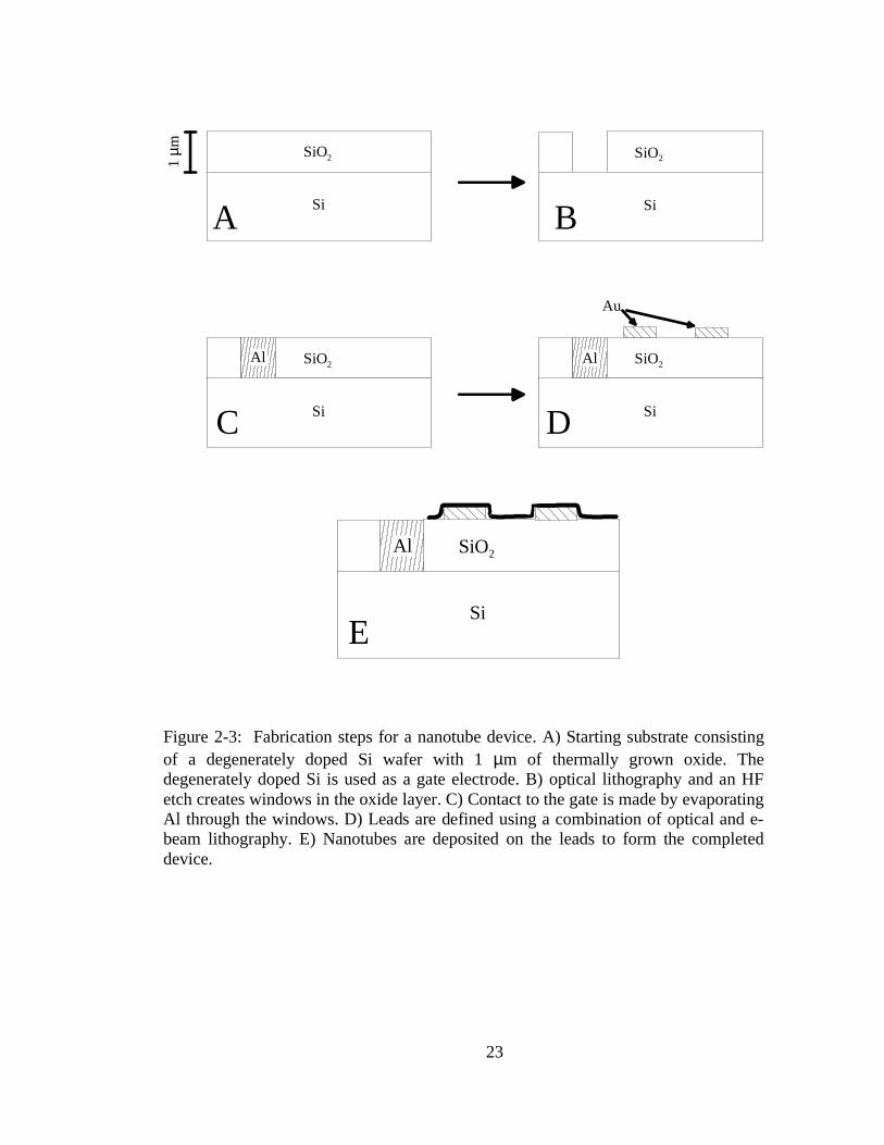
To attach leads to the nanotubes, we start with a degenerately doped Si wafer
that has 1 µm of thermal oxide grown on the surface. Optical lithography is used to etch
21
Figure 2-2: AFM image of tubes and ropes on SiO2. Faintest objects are ~1 nm in height. (Image courtesy of Michael Fuhrer.)
1 µm
22
holes in the oxide and define Al contacts to the degenerately doped Si, which is used as
a gate. In this procedure, the wafer is first covered with photoresist. Exposure to UV
light through a mask chemically changes the resist. The pattern defined by the mask is
then developed to produce holes in the resist layer. The wafer is then immersed in HF,
which removes the exposed oxide. Finally, Al is evaporated onto the wafer, and then
the unwanted metal is removed by lift-off. These steps are shown in Fig. 2-3A-C.
Starting with this wafer with back gate contacts, making electrical contact to the
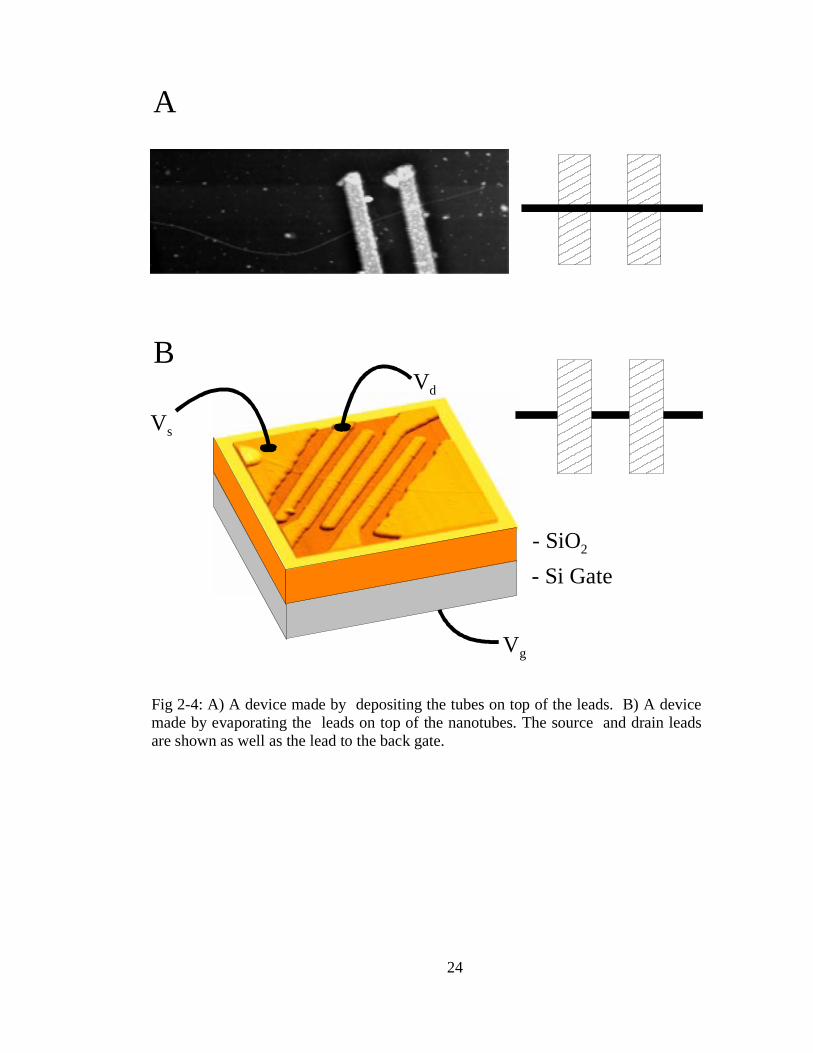
nanotubes is then done in either of two ways. In the first method[1], leads are first
defined using a combination of optical lithography and electron-beam lithography
(EBL) to make an array of 42 junctions on a few-mm by few-mm chip. Tubes are
deposited on top of the leads, as is shown schematically in Fig. 2-3D and 2-3E.
Promising candidate devices are then found by using a probe station to test the
electrical properties. These devices are then examined with an AFM to determine the
number and size of the nanotubes/bundles bridging the contacts. Figure 2-4A shows a
device made using this technique.
In the second method[2], nanotubes are deposited on an oxidized Si wafer that
has pre-defined alignment marks in addition to the back gate contacts. These alignment
marks consist of ~ 1 µm Au squares that were formed in a prior lithography step. A
suitable tube or bundle is located with an AFM, and its position is noted relative to the
alignment marks. A resist polymer (either PMMA or PMMA/MAA) is then spun on the
sample and leads to the nanotubes are defined with EBL. A completed device is shown
in Figure 2-4B.
23
Si
SiO2
Si
SiO2
Si
SiO2Al
Si
SiO2Al
Au
Si
SiO2Al
1 µ m
A B
C D
E
Figure 2-3: Fabrication steps for a nanotube device. A) Starting substrate consisting of a degenerately doped Si wafer with 1 µm of thermally grown oxide. The degenerately doped Si is used as a gate electrode. B) optical lithography and an HF etch creates windows in the oxide layer. C) Contact to the gate is made by evaporating Al through the windows. D) Leads are defined using a combination of optical and e-beam lithography. E) Nanotubes are deposited on the leads to form the completed device.
24
- SiO2
- Si Gate
Vg
Vs
Vd
Fig 2-4: A) A device made by depositing the tubes on top of the leads. B) A device made by evaporating the leads on top of the nanotubes. The source and drain leads are shown as well as the lead to the back gate.
B
A

25
In either method, once the leads have been attached, the device is mounted in a
chip package using colloidal silver paint. Electrical contact between the bonding pads
on the chip and the package is made by 2-mil Al wire, using ultrasonic wire bonding.
Finally, the package can then be inserted into standard 16-pin sockets and is ready for
electrical measurements.
2.2 Low Temperature Electrical Measurements
Making transport measurements of the samples requires that we apply voltages
and measure the resulting currents. To apply voltages to the sample, we use a standard
Windows PC computer with a National Instruments analog-to-digital (ADC) and
digital-to-analog (DAC) converter card. The voltages are applied via the output from
the DACs, which are software controlled. Using multiple DACs allows both a source-
drain voltage to be applied as well as a voltage on the gate. The current is measured
using an Ithaco current pre-amplifier that outputs a voltage proportional to the
measured current. This output voltage is read by the ADC and data acquisition software
allows the data to be plotted in real time.
The DACs can produce independent voltages from –10 V to +10 V with
approximately 0.5 mV resolution. Typically, the voltage applied to the sample is < 100
mV, and thus using the full range of the DAC is seldom necessary. Hence, depending
on the desired bias, the DAC output voltage can be divided down with a resistive
divider before appearing across the sample to sacrifice the full range of voltage for
increased resolution. For example, dividing by 100 gives a full range of –100 mV to
26
+100 mV with 5 µV resolution. A schematic of the typical measurement circuit is
shown in Figure 2-5.
To enable low-temperature measurements of nanotube devices, we have
employed several different methods. The simplest method involves dipping the package
into a partially filled liquid 4He dewar. By raising the sample above the liquid level, the
sample can be brought to equilibrium at different temperatures. The temperature is
measured by mounting a resistance thermometer near the sample. This allows
measurements over a temperature range from 4.2 K to approximately room
temperature.
For increased thermal stability and a temperature range from 1.4 K to 280 K, we
use an Oxford variable temperature system. This cryostat is designed to work while
immersed in liquid 4He (LHe.) The sample is isolated from the LHe by a vacuum
jacket. However, 4He may enter the sample space through a motorized needle valve and
heat exchanger. The temperature of the heat exchanger is regulated by a feedback
system, which can apply voltage to a heater and control the needle valve. By pumping
on the sample space, the sample temperature can then maintained by flowing 4He gas.
Finally, for the lowest temperature measurements, we have used an Oxford
Kelvinox 300 4He/3He dilution refrigerator (DR). This works as follows. A mixture of
3He and 4He is known to phase separate at low temperatures into a dilute and
concentrated phase. In the limit of zero temperature, the dilute phase will still be
approximately 6% 3He. In a DR, the cooling power is obtained by pumping the 3He

27
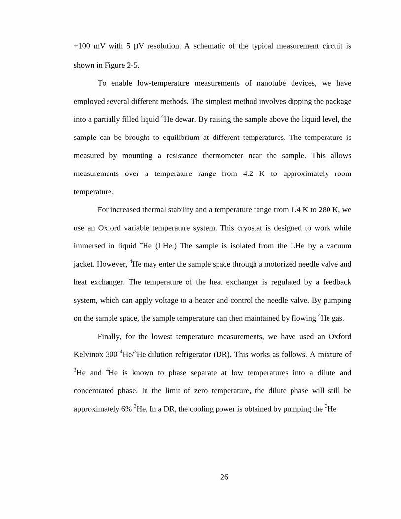
Vsd Vg
I
R1
R2
R3
C
Figure 2-5: Typical measurement setup. The nanotube device is indicated schematically by the dashed circle. The device consists of a nanotube contacted by two leads a gate electrode. A source-drain voltage is applied through the voltage divider formed by R1 and R2. The gate voltage Vg is applied through the low-pass filter formed by the resistor R3 and the capacitor C. R3 is typically one the order of 100 MΩ, which serves to protect the device in case of a gate oxide breakdown or some other mishap. The current though the device is measured with the Ithaco current amplifier as shown.
Voltage Divider
28
from the dilute phase. To restore the equilibrium concentration, 3He from the
concentrated phase must migrate across the phase boundary into the dilute phase. Since
the highest energy atoms leave preferentially, this cools the concentrated phase. The
3He removed from the dilute phase can be recondensed and returned to the mixture,
resulting in closed cycle refrigeration. The circulation rate can be increased
significantly by heating the dilute phase, and because there is always 3He present in the
dilute phase the DR can continue to provide cooling power down to extremely low
temperatures. In our lab, we typically reach a base temperature of ~50 mK.
2.3 Basic Observations
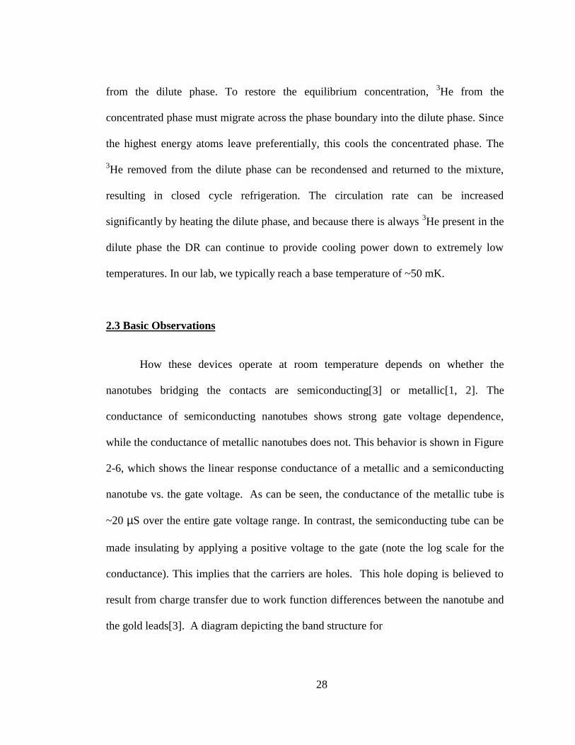
How these devices operate at room temperature depends on whether the
nanotubes bridging the contacts are semiconducting[3] or metallic[1, 2]. The
conductance of semiconducting nanotubes shows strong gate voltage dependence,
while the conductance of metallic nanotubes does not. This behavior is shown in Figure
2-6, which shows the linear response conductance of a metallic and a semiconducting
nanotube vs. the gate voltage. As can be seen, the conductance of the metallic tube is
~20 µS over the entire gate voltage range. In contrast, the semiconducting tube can be
made insulating by applying a positive voltage to the gate (note the log scale for the
conductance). This implies that the carriers are holes. This hole doping is believed to
result from charge transfer due to work function differences between the nanotube and
the gold leads[3]. A diagram depicting the band structure for

29
-4 -2 0 2 40
5
10
15
20
25
30
35
40
G (
µS)
Vg (V)
PHWDOOLF
EF
VHPLFRQGXFWLQJ
EF
-10 -8 -6 -4 -2 0 2 4 6 81E-8
1E-7
1E-6
1E-5
1E-4
1E-3
0.01
0.1
1
G (
µ S)
Vg (V)
Figure 2-6: A) A metallic tube. The conductance shows very little dependence on gate voltage. B) A semiconducting tube. The conductance shows a strong gate voltage dependence.
A
B

30
both types of nanotube is shown to the right of the data. We have performed extensive
low-temperature measurements on both types of nanotube, as will be discussed in detail
in the following chapters.
31
References
1 S. J. Tans, et al., Nature 386, 474 (1997).
2 M. Bockrath, et al., Science 275, 1922 (1997).
3 S. J. Tans, R. M. Verschueren, C. Dekker, Nature 393, 49 (1998).

32
Chapter 3
Single-Electron Transport in Ropes of Carbon Nanotubes
Marc Bockrath, David H. Cobden, Paul L. McEuen, Nasreen G. Chopra, and A. Zettl
Molecular Design Institute, Lawrence Berkeley National Laboratory and
Department of Physics, University of California at Berkeley, Berkeley, CA 94720, USA
Andreas Thess and R. E. Smalley
Center for Nanoscale Science and Technology, Rice Quantum Institute, and
Departments of Chemistry and Physics, Rice University MS-100, Rice University, P.O.
Box 1892, Houston, TX 77251, USA.
Abstract
The electrical properties of individual bundles, or "ropes," of single-walled carbon
nanotubes have been measured. Below ~10 Kelvin, the low bias conductance was
suppressed for voltages below a few millivolts. In addition, dramatic peaks were
observed in the conductance as a function of a gate voltage that modulated the number
of electrons in the rope. These results are interpreted in terms of single electron
charging and resonant tunneling through the quantized energy levels of the nanotubes
comprising the rope.
33
In the past decade, transport measurements have emerged as a primary tool for
exploring the properties of nanometer-scale structures. For example, studies of
quantum dots have illustrated that single-electron charging and resonant tunneling
through quantized energy levels regulate transport through small structures[1].
Recently, much attention has been focused on carbon nanotubes[2]. Their conducting
properties are predicted to depend upon the diameter and helicity of the tube,
parameterized by a rollup vector (n, m). One type of tube, the so-called (n, n), or
armchair, tube, is expected to be a one-dimensional (1D) conductor with current carried
by a pair of 1D subbands[3] whose dispersion relations near the Fermi energy EF are
indicated in the right inset to Fig. 3-1. A recent breakthrough has made it possible to
obtain large quantities of the (10,10) single-walled nanotube (SWNT), which is ~1.4
nm in diameter[4]. This advance, in combination with recent successes in performing
electrical measurements on individual multi-walled nanotubes (MWNTs)[5-8] and
nanotube bundles[9], makes possible the study of the electrical properties of this novel
1D system.
We have measured transport through bundles, or ropes, of nanotubes bridging contacts
separated by 200 to 500 nm. We find that a gap (suppressed conductance at low bias)
is observed in the current-voltage (I-V) curves at low temperatures. Further, dramatic
peaks are observed in the conductance as a function of a gate voltage Vg that modulates
the charge per unit length of the tubes. These observations are consistent with single-
electron transport through a segment of a single tube with a typical addition energy of ~
10 meV and an average level spacing of ~ 3 meV.

34
-40
-20
0
20
40
-6 -5 -4 -3 -2 -1 0 1 2 3 4 5 6
I (n
A) 1.3 K
290 K
V (mV)
Figure 3-1: The I-V characteristics at a series of different temperatures for the ropesegment between contacts 2 and 3. Left inset: an atomic force microscope (AFM)image of a completed device. The bright regions are the lithographically definedmetallic contacts, labeled 1-4. The rope is clearly visible as a brighter stripeunderneath the metallic contacts. In between the contacts (dark region) it is difficult tosee the rope because of the image contrast. Note that the width of the rope in the AFMimage reflects the convolution of its actual width with the AFM tip radius ofcurvature. The actual thickness of the rope is experimentally determined by themeasuring its height with the AFM and assuming that the rope is cylindrical. Rightinset: schematic energy-level diagram of the two 1D subbands near one of the twoDirac points [3], with the quantized energy levels indicated. The k-vector here pointsalong the tube axis.

35
The device geometry (Fig. 3-1, left inset) consists of a single nanotube rope to which
lithographically defined leads have been attached. The tubes are fabricated as
described in[4] and consist of ropes made up of ~1.4-nm diameter SWNTs.
Nanodiffraction studies[10] indicate that ~30 to 40% of these are (10,10) tubes.
Contacts were made to individual ropes as follows. First, the nanotube material was
ultrasonically dispersed in acetone and then dried onto an oxidized Si wafer on which
alignment marks had previously been defined. An atomic force microscope (AFM)
operating in the tapping mode was used to image the nanotubes. Once a suitable rope
was found, its position was noted relative to the alignment marks. Resist was then spun
over the sample, and electron beam lithography was used to define the lead geometry.
A metal evaporation of 3 nm Cr then 50 nm of Au followed by liftoff formed the leads.
This device has four contacts, and allows different segments of the rope to be measured
and four-terminal measurements to be performed. The rope is clearly seen underneath
the metal layer in the left inset to Fig. 3-1, although it is not visible in betweeen the
contacts because of the contrast of the image. The device was mounted on a standard
chip carrier, contacts were wire bonded, and the device was loaded into a 4He cryostat.
A dc bias could be applied to the chip carrier base to which the sample is attached. This
gate voltage Vg modified the charge density along the length of the rope. Four samples
were studied at liquid helium temperatures. All of the data presented here, however,
were obtained from a single 12 nm diameter rope containing ~60 SWNTs.
Figure 3-1 shows the I-V characteristics of the nanotube rope section between
contacts 2 and 3 as a function of T. The conductance is strongly suppressed near V = 0
for T < 10 K. Gaps of a similar magnitude were obtained for the other nanotube ropes
with diameters varying from 7 to 12 nm and lengths from 200 to 500 nm. There was
36
no clear trend in the size of the gap or the high-bias conductance with the rope length or
diameter. We note that measurements of MWNTs by ourselves and others[5,7,8]
displayed no such gap in their I-V curves. These results are in rough agreement,
however, with those reported previously by Fischer et al.[9] on similar, but longer,
ropes of SWNTs. In their experiments, the linear-response conductance also decreased
at low temperatures.
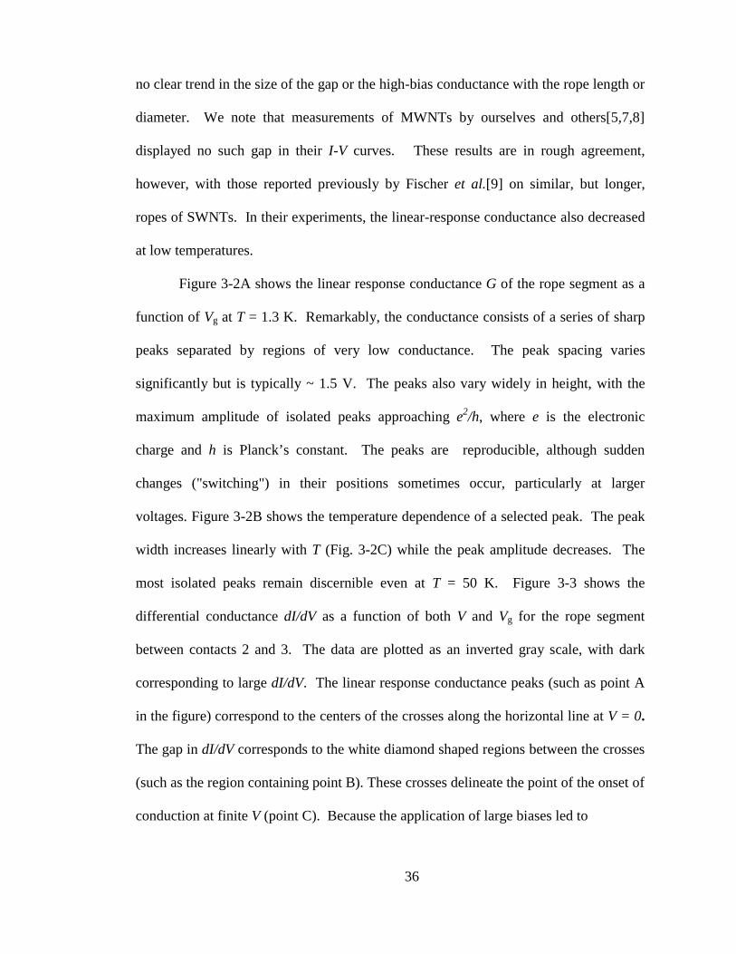
Figure 3-2A shows the linear response conductance G of the rope segment as a
function of Vg at T = 1.3 K. Remarkably, the conductance consists of a series of sharp
peaks separated by regions of very low conductance. The peak spacing varies
significantly but is typically ~ 1.5 V. The peaks also vary widely in height, with the
maximum amplitude of isolated peaks approaching e2/h, where e is the electronic
charge and h is Planck’s constant. The peaks are reproducible, although sudden
changes ("switching") in their positions sometimes occur, particularly at larger
voltages. Figure 3-2B shows the temperature dependence of a selected peak. The peak
width increases linearly with T (Fig. 3-2C) while the peak amplitude decreases. The
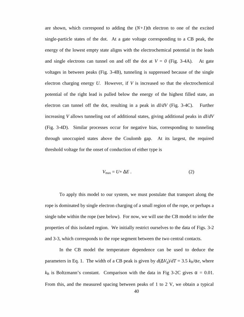
most isolated peaks remain discernible even at T = 50 K. Figure 3-3 shows the
differential conductance dI/dV as a function of both V and Vg for the rope segment
between contacts 2 and 3. The data are plotted as an inverted gray scale, with dark
corresponding to large dI/dV. The linear response conductance peaks (such as point A
in the figure) correspond to the centers of the crosses along the horizontal line at V = 0.
The gap in dI/dV corresponds to the white diamond shaped regions between the crosses
(such as the region containing point B). These crosses delineate the point of the onset of
conduction at finite V (point C). Because the application of large biases led to

37
16 18 20 22 24 26 28 300.0
0.2
0.4
0.6
0.8
1.0
AG
(e2 /h
)
Vg (V)25.2 25.4 25.6
0.0
0.1
T (K)
11
B
7
16
1.3
G (
e2 /h)
Vg (V)
0.0 0.5 1.00.0
0.1
0.2
0.3
0.4
C
Pea
k w
idth
(V
)
kBT (meV)
Figure 3-2: A) Conductance versus gate voltage at T =1.3 K for the rope segmentbetween contacts 2 and 3. B) Temperature dependence of a peak. Note that thispeak was measured on a different run from the data in A and does not directlycorrespond to any of the peaks there. C) Width of the peak in B as a function of T.

38
significant switching of the device, our sweeps were limited to ± 8 mV, and only the center
of the diamond regions are visible. Additional features (point D) are also observed above
the gap.
These results are reminiscent of previous measurements of Coulomb blockade
(CB) transport in metal and semiconductor wires and dots[1]. In these systems,
transport occurs by tunneling through an isolated segment of the conductor or dot that
is defined by either lithographic patterning or disorder. Tunneling on or off this dot is
governed by the single-electron addition and excitation energies for this small system.
The period of the peaks in gate voltage, ∆Vg, is determined by the energy for adding an
additional electron to the dot. In the simplest model that takes into account both
Coulomb interactions and energy level quantization, which we refer to as the CB
model, the peak spacing is given by
∆Vg = (U + ∆E)/eα , (1)
where U = e2/C is the Coulomb charging energy for adding an electron to the dot, ∆E is
the single-particle level spacing, and α = Cg/C is the rate at which the voltage applied to
the back gate changes the electrostatic potential of the dot. Here C is the total
capacitance of the dot and Cg is the capacitance between the dot and the back gate.
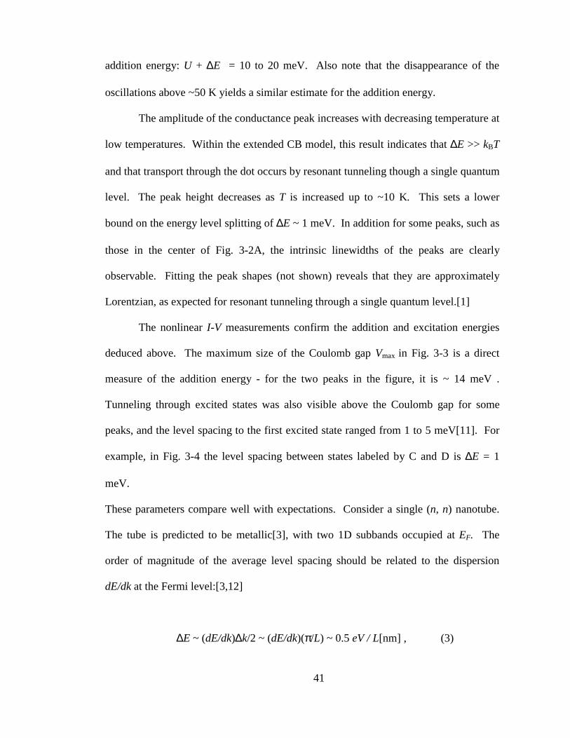
To understand the dependence on V and Vg in more detail, consider the energy
level diagrams in Fig. 3-4. They show a dot filled with N electrons, followed by a gap
U + ∆E for adding the (N+1)th electron. Above this, additional levels separated by ∆E

39
Vg (V)
CD
BAV (m
V)
-eVC
∆E
U+∆E
A B
C D
-eVD
••
•••
•••
•••
Figure 3-4: Schematic energy-level diagrams within the Coulomb blockade modelcorresponding to the points marked on Fig. 3: (A) at a Coulomb peak, where linear-response (V = 0) transport is possible; (B) between peaks, where linear-responsetransport is blockaded (the addition energy U+∆E and the level spacing ∆E areindicated here); (C) and (D) at two different applied voltages, where transport occursthrough the first and second occupied states respectively.
Figure 3-3: Gray scale plot of the differential conductance dI/dV of the rope segmentbetween contacts 2 and 3, as a function of V and Vg. To enhance the image contrast asmoothed version of the data was subtracted from the differential conductance. Thepoints marked A-D correspond to the diagrams in Fig. 4.
40
are shown, which correspond to adding the (N+1)th electron to one of the excited
single-particle states of the dot. At a gate voltage corresponding to a CB peak, the
energy of the lowest empty state aligns with the electrochemical potential in the leads
and single electrons can tunnel on and off the dot at V = 0 (Fig. 3-4A). At gate
voltages in between peaks (Fig. 3-4B), tunneling is suppressed because of the single
electron charging energy U. However, if V is increased so that the electrochemical
potential of the right lead is pulled below the energy of the highest filled state, an
electron can tunnel off the dot, resulting in a peak in dI/dV (Fig. 3-4C). Further
increasing V allows tunneling out of additional states, giving additional peaks in dI/dV
(Fig. 3-4D). Similar processes occur for negative bias, corresponding to tunneling
through unoccupied states above the Coulomb gap. At its largest, the required
threshold voltage for the onset of conduction of either type is
Vmax = U+ ∆E . (2)
To apply this model to our system, we must postulate that transport along the
rope is dominated by single electron charging of a small region of the rope, or perhaps a
single tube within the rope (see below). For now, we will use the CB model to infer the
properties of this isolated region. We initially restrict ourselves to the data of Figs. 3-2
and 3-3, which corresponds to the rope segment between the two central contacts.
In the CB model the temperature dependence can be used to deduce the
parameters in Eq. 1. The width of a CB peak is given by d(∆Vg)/dT = 3.5 kB/αe, where
kB is Boltzmann’s constant. Comparison with the data in Fig 3-2C gives α = 0.01.
From this, and the measured spacing between peaks of 1 to 2 V, we obtain a typical
41
addition energy: U + ∆E = 10 to 20 meV. Also note that the disappearance of the
oscillations above ~50 K yields a similar estimate for the addition energy.
The amplitude of the conductance peak increases with decreasing temperature at
low temperatures. Within the extended CB model, this result indicates that ∆E >> kBT
and that transport through the dot occurs by resonant tunneling though a single quantum
level. The peak height decreases as T is increased up to ~10 K. This sets a lower
bound on the energy level splitting of ∆E ~ 1 meV. In addition for some peaks, such as
those in the center of Fig. 3-2A, the intrinsic linewidths of the peaks are clearly
observable. Fitting the peak shapes (not shown) reveals that they are approximately
Lorentzian, as expected for resonant tunneling through a single quantum level.[1]
The nonlinear I-V measurements confirm the addition and excitation energies
deduced above. The maximum size of the Coulomb gap Vmax in Fig. 3-3 is a direct
measure of the addition energy - for the two peaks in the figure, it is ~ 14 meV .
Tunneling through excited states was also visible above the Coulomb gap for some
peaks, and the level spacing to the first excited state ranged from 1 to 5 meV[11]. For
example, in Fig. 3-4 the level spacing between states labeled by C and D is ∆E = 1
meV.
These parameters compare well with expectations. Consider a single (n, n) nanotube.
The tube is predicted to be metallic[3], with two 1D subbands occupied at EF. The
order of magnitude of the average level spacing should be related to the dispersion
dE/dk at the Fermi level:[3,12]
∆E ~ (dE/dk)∆k/2 ~ (dE/dk)(π/L) ~ 0.5 eV / L[nm] , (3)
42
where the 2 arises from non-degeneracy of the two 1D subbands (see Fig. 3-1, right
inset.) The charging energy is more difficult to estimate accurately. The actual
capacitance of the dot depends on the presence of the leads, the dielectric constant of
the substrate, and the detailed dielectric response of the rope[13]. For an order of
magnitude estimate, however, we take the capacitance to be given by the size of the
object, C = L. We then have:
Ue
C
e
L
eV
L nm= = ≈
2 2 14.
[ ]. (4)
Note the remarkable result that in 1D, both ∆E and U (Eqs. 3 and 4) scale as 1/L, and
hence the ratio of the charging energy to the level spacing is roughly independent of
length. This means that the level spacing will be important even in fairly large dots,
unlike in 3D systems. For a length of tube L ~ 200 nm (the spacing between the leads)
we obtain U = 7 meV and ∆E = 2.5 meV, consistent with the observed values.
To relate these theoretical results for a single tube to the measurements of rope
samples, we first note that current in the rope is likely to flow along a filamentary
pathway[14] consisting of a limited number of single tubes or few-tube segments. This
is because, first, 60 to 70 % of the tubes are not (10,10), and hence the majority of the
tubes in the rope will be insulating at low T[15]. Second, the intertube conductance is
small compared to the conductance along the tube, inhibiting intertube transport.
Finally, the metal probably only makes contact to those metallic tubes which are on the
surface of the rope, further limiting the number of tubes involved in transport.

43
Disorder along a filamentary pathway will tend to break it up into weakly
coupled localized regions. This disorder may result from defects[17], twists[18], or
places where intertube hopping is necessary along the pathway. Generally, the
conductance should then determined by single electron charging and tunneling between
a few such localized regions. For other rope segments that we have measured, the
characteristics were consistent with transport through a few segments in series or
parallel, each with different charging energies. For the particular rope segment we have
focused on here, however, a single well defined set of CB peaks was observed,
indicating that transport was dominated by a single localized region. We believe this
region is a section of a single tube, or at most a few-tube bundle. The measured
charging energies and level spacing indicate that the size of this region is roughly the
length between the contacts.
Each peak therefore corresponds to resonant tunneling though a coherent
molecular state that extends for up to hundreds of nanometers in a localized region
within the nanotube bundle. Furthermore, the amplitudes of some isolated peaks
approach the theoretical maximum for single-electron transport of e2/h. This is only
possible if the barriers which confine this state at either end are approximately equal,
and there is no other significant resistance in series with the localized region. This is
consistent with the barriers being at the contacts between the metal leads and the rope.
It is also possible that the barriers are within the rope, in which case the metal-rope
contacts must be almost ideal so as not to reduce the maximum conductance from
e2/h[16]. Variation in the coupling to each lead from level to level can account for the
varying peak sizes apparent in Fig. 3-2.

44
Although the above interpretation accounts for the major features in the data,
many interesting aspects of this system remain to be explored. First, one would like to
establish absolutely that transport is indeed occurring predominantly along a single
tube. Second, it should be determined whether all details of the data can be explained
within the simple CB model discussed above, since Coulomb interactions may
significantly modify the low-energy states from simple 1D non-interacting levels[19].
Of great interest would be measurements of disorder-free tubes, where the intrinsic
conducting properties of the tube can be measured without the complications of single-
electron charging. To address these issues, experiments on individual single-walled
tubes are highly desirable, and progress is being made in this direction[20]. Yet
another important experiment would be to measure directly the intertube coupling by
making separate electrical contact to two adjacent tubes.

45
References
A similar version of Chapter 3 appeared in Science 275 1922 (1997).
1 For a review, see Single Charge Tunneling, edited by H. Grabert and M.H.
Devoret (Plenum Press, NY, 1991); M. Kastner, Physics Today, 46, 24 (1993); Leo P.
Kouwenhoven and P.L. McEuen, Nanoscience and Technology, G. Timp, ed. (AIP
Press, NY), to be published.
2 S. Iijima, Nature 354, 56 (1991); for a recent review, see T. Ebbesen, Physics
Today, 49, 26 (1996).
3 R. Saito, M. Fujita, G. Dresselhaus, and M.S. Dresselhaus, Appl. Phys. Lett. 60,
2204 (1992); N. Hamada, S. Sawada, and A. Oshiyama, Phys. Rev. Lett. 68, 1579
(1992).
4 A. Thess et al., Science 273, 483 (1996).
5 L. Langer et al., Phys. Rev. Lett. 76, 479, (1996).
6 H. Dai, E.W. Wong, and C.M. Lieber, Science 272, 523 (1996).
7 T.W. Ebbesen et al., Nature 382, 54 (1996).
8 A. Yu. Kasumov, I.I. Khodos, P.M. Ajayan, and C. Colliex, Europhys. Lett. 34,
429 (1996).
9 J. E. Fischer et al, Phys. Rev. B. 55, 4921 (1997).
10 D. Bernaerts, A. Zettl, N. G. Chopra, A. Thess, R. E. Smalley, Solid State
Communications 105, 145-9 (1998); J. M. Cowley, P. Nikolaev, A. Thess, and R. E.
Smalley, Chem. Phys. Lett. 265, 379 (1997).
11 The level spacing can be determined from the data in Fig. 3-3 by two means.
The first means is to measure the separation between features in Vg, and employ the
46
conversion factor α = Vmax/∆Vg. The second is to measure the separation between the
features in V, and use the slopes of the lines defining the Coulomb gap to infer αL=
CL/C and αR = CR/C. For more information, see Ref [1].
12 H.-Y. Zhu, D. J. Klein, T. G. Schmalz, N. H. Rubio, and N. H. March, preprint
(1997).
13 L. X. Benedict, S. G. Louie, and M. L. Cohen, Phys. Rev. B, 52, 8541 (1995).
14 Other measurements on these samples also support the notion that transport is
through individual decoupled tubes. In four terminal measurements of the ropes at
temperatures > 30 K (where the rope resistance becomes much less than the voltage
probe impedance and reliable four-terminal measurements are possible), non-local
voltages have been observed. For example, referring to the AFM image shown in Fig.
3-1, a voltage can appear between the terminals 1 and 2 in response to a current flowing
between contacts 3 and 4. Such non-local effects are possible if different contacts make
contact to different tubes and the intertube coupling is small. Current injected into 4 in
a particular tube that is not well connected to 3 can arrive at contact 1 or 2, producing a
non-local response.
15 Individual tubes within a rope have chiral angles within 10o of the achiral
(10,10) tube with roughly 30 to 40% of the sample being (10,10) tubes [10]. The
indices of tubes consistent with the experimental constraints on chirality and radius [4]
are (10,10), (9,11), (8,12), (7,13) and the opposite-handed twins. The gap of the (7,13)
tube is small and likely does not survive intertube interactions, but the gaps of the
(9,11) and (8,12) tubes are about 0.5 eV, which is probably large enough to maintain
semiconducting behavior within the rope.

47
16 The large peak heights, combined with the fact that the room temperature
conductance of the center segment is also approximately e2/h, imply that good electrical
contact has been made between the metal leads and part of the rope.
17 L. Chico, L. X. Benedict, S. G. Louie, and M. L. Cohen, Phys. Rev. B 54, 2600
(1996); L. Chico et al. Phys. Rev. Lett. 76, 971 (1996).
18 C.L. Kane and E.J. Mele, to be published in Physical Review Letters.
19 Y. A. Krotov, D.-H. Lee, S. G. Louie, Phys. Rev. Lett. 78, 4245 (1997); C.
Kane, L. Balents, M. P. A. Fisher, Phys. Rev. Lett. 79, 5086 (1997).
20 S. Tans, et al., Nature 386, 474 (1997).
21 We would like to acknowledge useful discussions with V. Crespi, M. Cohen,
D.H. Lee, and S. Louie. We are also indebted to S. Tans for communicating his
unpublished results on measurements on nanotubes and emphasizing the importance of
a gate voltage. Supported by the U.S. Department of Energy under Contract No. DE-
AC03-76SF00098 and by the Office of Naval Research, Order No. N00014-95-F-0099.
48
Chapter 4
Spin Splitting and Even-Odd Effects in Carbon Nanotubes
David H. Cobden, Marc Bockrath, and Paul L. McEuen
Department of Physics, University of California and Materials Science Division,
Lawrence Berkeley National Laboratory, Berkeley, California, 94720
Andrew G. Rinzler and Richard E. Smalley
Center for Nanoscale Science and Technology, Rice Quantum Institute, and
Department of Chemistry and Physics, MS-100, Rice University, P.O. Box 1892,
Houston, TX 77251
Abstract
The level spectrum of a single-walled carbon nanotube rope, studied by transport
spectroscopy, shows Zeeman splitting in a magnetic field parallel to the tube axis. The
pattern of splittings implies that the spin of the ground state alternates by ½ as
consecutive electrons are added. Other aspects of the Coulomb blockade characteristics,
including the current-voltage traces and peak heights, also show corresponding even-odd
effects.
49
The spin state of small multi-electron systems is an important testing ground for
our understanding of interacting quantum systems. For N non-interacting electrons in
non-degenerate levels with spin, the single-particle states are occupied in order of
energy, leading to a total spin S = 0 for even N and S = 1/2 for odd N. Coulomb
interactions among the electrons can alter this behavior, however. In atoms, for
example, the exchange interaction among electrons in a shell leads to Hund’s rule and a
spin-polarized ground state for a partially filled shell. Recently, attention has been
focused on similar questions in quantum dots. In small 3D metallic dots, Zeeman
splitting consistent with an alternation between S = 0 and 1/2 was found [1]. This may
be understood within the constant interaction (CI) model [2], where the energy for
adding an electron is the non-interacting level spacing ∆E plus a constant charging
energy U. On the other hand, in two-dimensional dots evidence for spin polarization in
the ground state has been found in recent experiments on both high symmetry [3] and
low symmetry dots [4], requiring explanations beyond the CI model.
Of considerable interest is the situation in 1D, where Coulomb interactions are
predicted to profoundly influence the properties of the system [5]. Here exact
theoretical results are available for many model systems. For instance, for electrons in a
box in strictly one dimension (1D), Lieb and Mattis [6] proved that in spite of
interactions the ground state has the lowest possible spin. In real systems, however, a
variety of factors, such as finite transverse dimensions, multiple 1D subbands, and spin-
orbit coupling, may lead to a spin-polarized ground state.
Here we present measurements of the spin state of single-walled carbon
nanotubes, a novel quasi-1D conductor where the current is carried by two 1D subbands
50
[7]. It has recently been shown experimentally [8,9] that when contacts are attached,
these nanotubes behave as quasi-1D quantum dots. Here we concentrate on a very short
(~200 nm) nanotube dot with a correspondingly large level spacing. To study the spin
state, we apply a magnetic field along the axis of the nanotube and examine the Zeeman
effects in the transport spectrum. From the pattern of the spin splitting, we conclude that
as successive electrons are added the ground state spin oscillates between S0 and S0+1/2,
where S0 is most likely zero. This results in an even/odd nature of the Coulomb peaks
which is also manifested in the asymmetry of the current-voltage characteristics and the
peak height. It may also be reflected in the excited state spectrum.
The devices are made [9] by depositing single-walled nanotubes [10] from a
suspension in dichloroethane onto 1-µm thick SiO2. The degenerately doped silicon
substrate is used as a gate electrode. A single rope is located relative to prefabricated
gold alignment marks using an atomic force microscope (AFM). Chromium-gold
contacts are then deposited on top using 20 keV electron beam lithography. An AFM
image of a 5-nm diameter rope (consisting of about a dozen tubes) with six contacts is
shown in the inset to Fig. 4-1. Leads labeled s (source), d (drain) and Vg (gate) are
drawn in to indicate the typical measurement configuration.
Figure 4-1 shows the linear-response two-terminal conductance, G, versus gate
voltage, Vg, at magnetic field B = 0 and temperature T = 100 mK. It exhibits a series of
sharp Coulomb blockade oscillations [8,9,2] that occur each time an electron is added to
the nanotube dot. For T <~ 10 K all the peaks have the same width, proportional to T
[9], and a T-independent area, indicating that the level spacing ∆E is >> kBT and that

51
Vg1 µm
sd
P1P0
-2 0 2
0
2
4
Vg (V)
(µ)
T = 100 mK
P2
P3
Figure 4-1: A) Conductance G of a nanotube rope vs gate voltage Vg. Inset: AFMimage of a device with schematic wires added.

52
V (
mV
)
Vg (V)
V (
mV
)
B = 0 T
B = 5 T
P0 P1
X Y Z
UV
WT
(a)
(b)
X Y ZU WT V
(c)
0
10
0.0 0.1 0.2 0.3 0.4
∆Vg (V)
B (
T)
Figure 4-2: A) Greyscale plot of the differential conductance dI/dV of Coulombpeaks P0 and P1 at B = 0 (darker = more positive dI/dV.) B) Same as A but at B= 5 T. C) B-dependence of the relative positions of the peak in dI/dV labeled T-Z in A, at a bias of V = -7 mV as indicated by the dashed line in A. On the x-axis we plot ∆Vg = Vg - Vg
T, where VgT is the position of peak T, to remove
unreproducible temporal drift of the characteristics along the Vg - axis.

53
transport is through a single quantum level. We deduce that the dot electrostatic
potential Vdot is linearly related to Vg, with a coefficient α ≡ dVdot/dVg = 0.09.
Figure 4-2A is a greyscale plot of the differential conductance dI/dV as a
function of V and Vg at B = 0. Dark lines here are loci of peaks in dI/dV. Crosses P0 and
P1 are formed by the identically labeled Coulomb peaks in Fig. 4-1. The interpretation
of such a plot in the CI model is well known [3]. Each line is produced by the alignment
of a quantized energy level in the dot with the Fermi level in a contact. From the
spacing of the lines we infer a typical level spacing ∆E ~ 5 meV, and from the average
Coulomb peak spacing we obtain a charging energy U ~ 25 meV. These values are
consistent with expectations based on previous measurements [8,9] for a 100-200 nm
length of tube. Thus we find as before [9] that the portion of nanotube rope forming the
dot appears roughly equal in length to the distance between the contacts (nominally 200
nm.)
Figure 4-2B shows the results of the same measurement at B = 5 T. Most of the
lines observed at B = 0 have split into parallel pairs. The splitting is linearly
proportional to B. This can be seen in Fig. 4-2 C, where the relative positions of the
peaks in dI/dV at V = -7 mV (dotted line in Fig. 4-2A) are plotted as a function of B.
One group of peaks (denoted by open symbols) moves downwards in Vg relative to the
other (solid symbols) by an amount proportional to B. Note that not all the lines at B = 0
split. Over a series of ten consecutive crosses in the range -2 V < Vg < +1 V [11], the
following pattern emerges: on alternate peaks, (P0, P2, etc.,) the leftmost lines in the
cross (such as T) do not split, while on the other peaks, (P1, P3, etc.,) the rightmost lines
(such as Z) do not split.
54
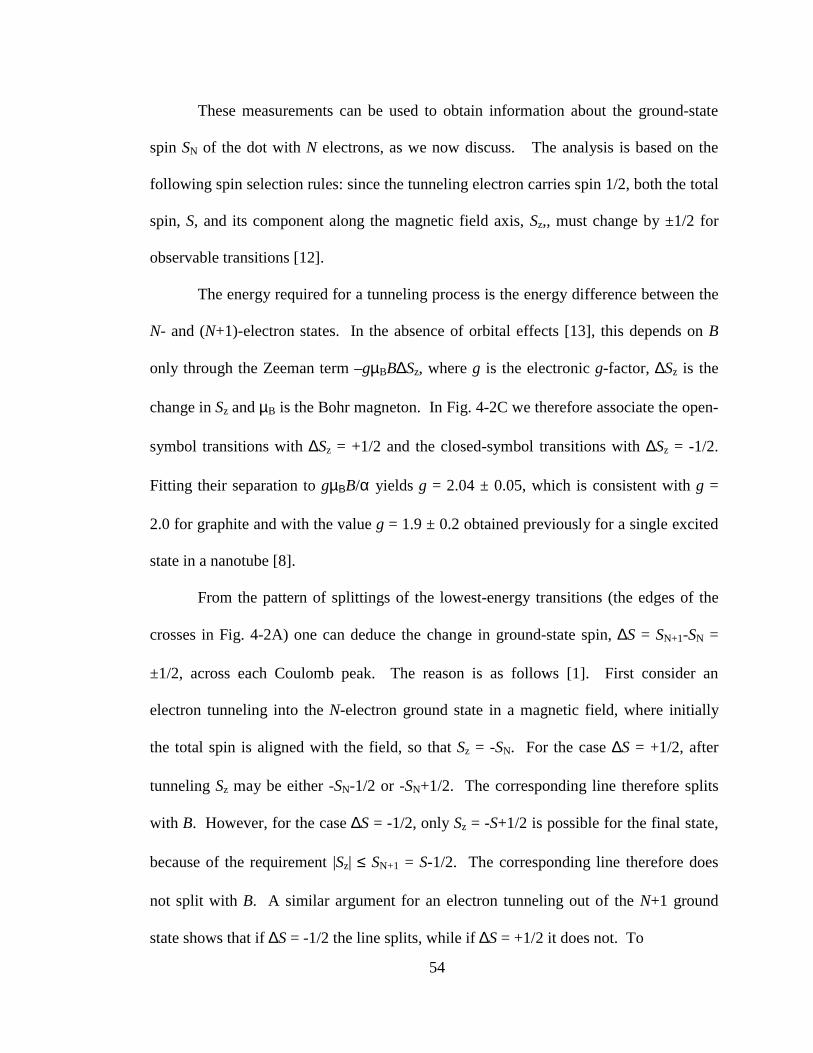
These measurements can be used to obtain information about the ground-state
spin SN of the dot with N electrons, as we now discuss. The analysis is based on the
following spin selection rules: since the tunneling electron carries spin 1/2, both the total
spin, S, and its component along the magnetic field axis, Sz,, must change by ±1/2 for
observable transitions [12].
The energy required for a tunneling process is the energy difference between the
N- and (N+1)-electron states. In the absence of orbital effects [13], this depends on B
only through the Zeeman term –gµBB∆Sz, where g is the electronic g-factor, ∆Sz is the
change in Sz and µB is the Bohr magneton. In Fig. 4-2C we therefore associate the open-
symbol transitions with ∆Sz = +1/2 and the closed-symbol transitions with ∆Sz = -1/2.
Fitting their separation to gµΒB/α yields g = 2.04 ± 0.05, which is consistent with g =
2.0 for graphite and with the value g = 1.9 ± 0.2 obtained previously for a single excited
state in a nanotube [8].
From the pattern of splittings of the lowest-energy transitions (the edges of the
crosses in Fig. 4-2A) one can deduce the change in ground-state spin, ∆S = SN+1-SN =
±1/2, across each Coulomb peak. The reason is as follows [1]. First consider an
electron tunneling into the N-electron ground state in a magnetic field, where initially
the total spin is aligned with the field, so that Sz = -SN. For the case ∆S = +1/2, after
tunneling Sz may be either -SN-1/2 or -SN+1/2. The corresponding line therefore splits
with B. However, for the case ∆S = -1/2, only Sz = -S+1/2 is possible for the final state,
because of the requirement |Sz| ≤ SN+1 = S-1/2. The corresponding line therefore does
not split with B. A similar argument for an electron tunneling out of the N+1 ground
state shows that if ∆S = -1/2 the line splits, while if ∆S = +1/2 it does not. To

55
U+∆EgµBB
Odd peak Even peak
Figure 4-3: Explanation of splitting pattern within the CB model. Thelowest-energy transition splits for an odd peak (left), where N changes fromeven to odd, but not for an even peak (right), where N changes from odd toeven.

56
summarize: if ∆S = +1/2 for a Coulomb peak, the lines on the right edge of the cross do
not split, while if ∆S = -1/2 the lines on the left edge do not split.
This general result is also predicted by the CI model, as indicated in Fig. 4-3. If
N is even, SN = 0, and the next electron can be added to either spin-up or spin-down state
of the next orbital level (left sketch), resulting in SN+1 = 1/2. On the other hand, if N is
odd, SN = 1/2 and the next electron can only be added to the one empty spin state of that
level (right sketch), resulting in SN+1 = 0. A corresponding story can be told for
removing an electron. The predicted pattern of splittings is the same as in the previous
paragraph, but with the additional implication that N is even if ∆S = +1/2 and odd if ∆S
= -1/2.
Comparing the above predictions with Fig. 4-2, we find that ∆S = +1/2 for peak
P0 and ∆S = -1/2 for peak P1. Since the pattern of splitting alternates between the two
types over ten Coulomb peaks, we deduce that SN oscillates between some value S0 and
S0+1/2 as ten successive electrons are added. We cannot rule out the possibility that S0
is finite. However, since polarization of a system is usually related to states near the
Fermi level, and in this system we see the spin alternating as these states are filled, it is
most likely that that S0 = 0, as in the CI model. If this is the case, the behavior is
consistent with the prediction of Ref. [6] for 1D electrons: the ground state spin
alternates between 0 and 1/2. This is our principal result. We subsequently describe
Coulomb peaks where N changes from odd to even (P0, P2, etc.) as even peaks, because
the added electron is even. Peaks P1, P3, etc. we call odd peaks, because the added
electron is odd. This is indicated in Fig. 4-3.

57
The alternating spin of the ground state should also be reflected in the I-V
characteristics at zero magnetic field, if the source and drain contacts have different
tunnel resistances. If, for instance, the source contact dominates the resistance, the
magnitude of the current I- at negative source bias V is determined by transitions from
the N to the N+1 electron ground state, as long as the bias is less than the level spacing.
On the other hand, the current I+ at positive V is determined by transitions from the N+1
to the N electron ground state. The ratio β = I+/I- therefore reflects the differences
caused by the spin selection rules in these two situations. This can easily be understood
in the CI model, as illustrated for an even peak (∆S = -1/2) in Fig. 4-4A. For negative V
(left sketch) an electron tunneling in from the source can only go into one available spin
state. On the other hand, for positive V (right sketch), either of two electrons can tunnel
out. The current is therefore larger for positive V. An elementary calculation gives β =
(2Gs+Gd)/(Gs+2Gd), where Gs and Gd are the source and drain barrier conductances
respectively. For Gs < Gd, this predicts 1 < β < 2. In contrast, for an odd peak (∆S =
+1/2), the inverse ratio is found, and 1/2 < β < 1 is predicted.
The solid line in fig. 4-4B is the I-V characteristic measured at the center of peak
P0. Near V = 0, the I-V is ohmic, but for |V| >~ 0.5 mV the current saturates into a
slowly varying form. The saturation current is larger for positive than for negative V.
Moreover, if the same data is plotted (dashed line) with the current scaled by a factor -β,
where β = 1.57, the I-V’s in the two bias directions can be brought onto the same
interpolated curve (dotted line.) For each peak an appropriate value of β can be chosen
to achieve a similar matching. The results are plotted in the top panel of Fig. 4-4C. We
find that 1 < β < 2 for P0 and P2, while 1/2 < β < 1 for P1 and P3. Comparing these

58
-V
-2 0 2-0.2
0.0
0.2 Current as measured Current multiplied by -β
I (n
A)
V (mV)
P0 β = 1.57
(a)
(c)
(b)
0.0 1.0
0
1
P3P2P1P0
G (µ
S)
Vg (V)
0
1
2
β
Figure 4-4: A) Current flow at high bias in the CI model. Only the largerbarrier, between source and dot, is drawn. B) Solid line: I-V measured at thecenter of peak P0 in Figure 4-1. Dashed line: the same trace with I multipliedby -β = -1.57. Dotted line: interpolation between these. C) Lower: expandedview of the peaks P0 - P3. Upper: measured values of β for these peaks. Theoscillating value of β implies that successive electrons are added withopposite spin directions (see text).

59
values with the predictions for β = I+/I- in the previous paragraph, we see that they are
perfectly consistent with our assignments of ∆S = +1/2 or -1/2 from the Zeeman splitting
[14].
We have seen from the Zeeman splitting and the I-V characteristics that the
ground state spin behaves as is predicted by the CI model. However, this implies not
that effects such as exchange are small, but only that they do not change the spin of the
N-electron ground state of the system. Exchange might for instance be manifested in the
excited state spectra, where one would anticipate a difference between even and odd
peaks. For odd peaks, the added electron simply goes into higher unoccupied orbital
levels, giving rise to a single-particle spectrum. For even peaks, however, the added
electron can form singlet and triplet states with the original unpaired electron, leading to
exchange splitting. A singlet-triplet splitting has indeed been seen in the excitation
spectra of semiconductor dots [15]. We observe indications of this predicted behavior in
peaks P0-P3. The lowest excited states visible at negative V on even peaks in each case
form a pair (such as lines U and V on peak P0 in Fig. 4-2A), while those on odd peaks
do not (such as line Y on P1). This will be investigated further in future work.
A contradiction with the CI model is also seen in the peak heights. These are
predicted to be identical for a pair of peaks arising from a single orbital level [16].
However, we find that the odd peaks tend to be considerably larger than the even peaks,
as apparent in Fig. 4-4C. This behavior is not understood and deserves further
investigation.

60
In summary, our transport measurements of a short nanotube quantum dot show
that the ground state of this 1D electronic system alternates between S = 0 and S = 1/2.
A variety of even-odd effects are seen in the addition spectrum, some of which, such as
an alternation of the peak heights, require explanations beyond the simple Coulomb
blockade picture.
We thank Marvin Cohen, Cees Dekker, Noah Kubow, Dung-Hai Lee, Steven
Louie, Jia Lu, Boris Muzykantskii, and Sander Tans for helpful discussions. The work
at LBNL was supported by the Office of Naval Research, Order No. N00014-95-F-0099
through the U.S. Department of Energy under Contract No. DE-AC03-76SF00098, and
by the Packard Foundation. The work at Rice was funded in part by the National
Science Foundation and the Robert A. Welch Foundation
.

61
References
A similar version of Chapter 4 appeared in Phys. Rev. Lett. 81 681 (1998).
1 D. C. Ralph, C. T. Black, and M. Tinkham, Phys. Rev. Lett. 74, 3241 (1995);
Phys. Rev. Lett. 78, 4087 (1997).
2 L. P. Kouwenhoven et al., in Mesoscopic Electron Transport, Eds. L. P.
Kouwenhoven, G. Schon and L. L. Sohn (Kluwer, 1997).
3 S. Tarucha et al., Phys. Rev. Lett. 77, 3613 (1996).
4 D. R. Stewart et al., Science 278, 1784 (1998).
5 See, e.g., The Many-Body Problem, Ed. D. C. Mattis (World Scientific,
Singapore, 1993).
6 E. Lieb and D. Mattis, Phys. Rev. 125, 164 (1962).
7 N. Hamada, S. Sawada, and A. Oshiyama, Phys. Rev. Lett. 68, 1579 (1992); R.
Saito et al., Appl. Phys. Lett. 60, 2204 (1992).
8 S. J. Tans et al., Nature 386, 474 (1997).
9 M. Bockrath et al., Science 275, 1922 (1997).
10 A. Thess et al., Science 273, 483 (1996).
11 Outside this range of Vg the characteristics are complicated by charging of
another dot (probably another section of nanotube.)
12 D. Weinmann, W. Hausler, and B. Kramer, Phys. Rev. Lett. 74, 984 (1995).
13 The only expected orbital effect of an axial magnetic field results from the
Aharonov-Bohm phase due to the flux φ through the tube [17], which may shift the
levels by up to ~ 2.5 meV at 12 T. In our data the non-Zeeman energy shifts of the
transitions at this field are less than 100 µeV. This can be accounted for if all levels are
62
shifted equally, as expected if the Fermi level is displaced away from the band-crossing
points by, for example, charge transfer from the metal contacts [18].
14 From a detailed study of the I-V’s in this range of Vg we can deduce that Gs < Gd.
The gradual increase of |I| as V becomes more positive in Figure 4-4B is explained by
electric-field lowering of the dominating source barrier, as indicated in Figure 4-4A.
15 L. P. Kouwenhoven et al., Science 278, 1788 (1997).
16 C. W. J. Beenakker, Phys. Rev. B 44, 1646 (1991).

63
Chapter 5
Chemical Doping of Individual Semiconducting Carbon Nanotube Ropes
Marc Bockrath, J. Hone, A. Zettl, and Paul L. McEuen
Department of Physics, University of California and Materials Science Division,
Lawrence Berkeley National Laboratory, Berkeley, California, 94720
Andrew G. Rinzler and Richard E. Smalley
Center for Nanoscale Science and Technology, Rice Quantum Institute, and
Department of Chemistry and Physics, MS-100, Rice University, P.O. Box 1892,
Houston, TX 77251
(April 2, 1999)
Abstract
We report the effects of potassium doping on the conductance of individual
semiconducting single walled carbon nanotube ropes. We are able to control the level of
doping by reversibly intercalating and de-intercalating potassium. After doping, the
carriers are electrons. Typical values for the doping level are found to be ~ 100-1000
electrons/µm. The effective mobility for the electrons is µeff ~ 20-60 cm2 V-1 s-1, a value
similar to that reported for the hole effective mobility in nanotubes[1].
64
Recently, much attention has been focused on the transport properties of ~1-2 nm
diameter single-walled carbon nanotubes (SWNTs). The band structure of a given
SWNT depends on its chirality and is either a one-dimensional (1-D) metal or a 1-D
semiconductor with a band gap on the order of 0.6 eV[2, 3]. Recent work has shown
that semiconducting nanotubes can exhibit transistor action that is similar in operation to
a MOSFET[1, 4]. In these experiments, a gate electrode is used to electrostatically vary
the charge density in the nanotubes. The dependence of the conductance on the carrier
density indicates that the carriers added to the tubes are holes.
Besides using a gate, another way to change the charge density in a
semiconductor is by chemical doping. Previous work on mats of SWNTs has shown
that potassium acts an electron donor to the nanotubes[5] and that their conductance is
increased significantly by doping with potassium vapor[6, 7]. However, the
interpretation of these experiments is complicated by the fact that mats consist of both
semiconducting and metallic nanotubes, and that transport through the mats includes
hopping between nanotubes and/or bundles.
Here we report the controlled chemical doping of semiconducting nanotube
ropes with potassium. After doping, the carriers in the doped ropes are electrons. We
estimate the number of carriers added and hence the number of intercalated potassium
atoms. In addition we determine an effective mobility µeff for the electrons, which is
found to be similar in magnitude to the value reported for holes[1].
The samples are made by placing ropes on top of Au electrodes that have 500 nm
separation[8] as shown in the inset to Fig. 5-2. These electrodes are on top of a

65
degenerately doped oxidized Si wafer[9]. The degenerately doped substrate is used as a
gate. Once the samples are made, semiconducting and metallic devices are
distinguished by their room temperature conductance behavior with respect to gate
voltage. The conductance of metallic tubes shows relatively little dependence on gate
voltage, whereas the conductance of semiconducting nanotubes shows a very strong
dependence[4, 10]. An example of semiconducting behavior is shown in Fig. 5-1. The
open circles in Fig. 5-1 show the conductance of a 3 nm diameter rope with as a function
of gate voltage. At positive gate voltages, the conductance of the rope approaches zero.
As a negative gate voltage is applied, the conductance begins to increase as holes are
added to the rope[4]. This increase in conductance is approximately linear in gate
voltage. A similar slope has been found in all the samples we have studied to within a
factor of three.
Once we have obtained samples that show the above semiconducting behavior,
we then dope them with potassium. These doping experiments were carried out in a
controlled environment to prevent the potassium from reacting chemically with oxygen.
The doping vessel is essentially a glass tube that has wire feedthroughs in order to
enable transport measurements. A diagram of the doping vessel is shown in the inset of
Fig. 5-2. In an argon atmosphere, potassium is placed in the doping vessel at the
opposite end from the sample. The potassium end of the doping vessel is then sealed
with a
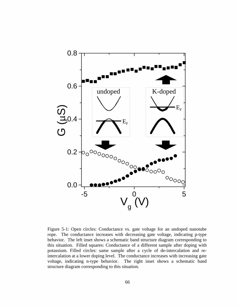
66
-5 0 50.0
0.2
0.4
0.6
0.8
G (
µS)
Vg (V)
EF
EF
undoped K-doped
Figure 5-1: Open circles: Conductance vs. gate voltage for an undoped nanotuberope. The conductance increases with decreasing gate voltage, indicating p-typebehavior. The left inset shows a schematic band structure diagram corresponding tothis situation. Filled squares: Conductance of a different sample after doping withpotassium. Filled circles: same sample after a cycle of de-intercalation and re-intercalation at a lower doping level. The conductance increases with increasing gatevoltage, indicating n-type behavior. The right inset shows a schematic bandstructure diagram corresponding to this situation.

67
0 1 2 3 4 5 6 70.0
0.1
0.2
0.3
0.4
0.5
0.6
0.7
D
E
B
C
AG
(µS
)
Time (hr)
Doping Vessel
500 nm
gate
source drain
K+
e-
Ts TK
potassiumvapor
sample
Figure 5-2: Main panel: Conductance of potassium-doped semiconducting samplevs. time. At point A heat was applied to the sample to de-intercalate potassiumfrom the doped sample. At point B heating was stopped temporarily. At point Cfurther heating resulted in the sample becoming insulating. Heat was then appliedto the potassium. At point D, the vapor pressure of the potassium is sufficient tobegin doping the sample. At point E, heating is stopped and the entire vesselbegins to return to room temperature. Inset: diagram of doping vessel and devicegeometry.

68
valve. Finally, the vessel is connected to a pump and is evacuated through the attached
valve.
The doping vessel is heated differentially by heaters on each end of the vessel.
The temperature at each end is measured with thermocouples. The temperature at the
sample end is denoted by Ts and the temperature at the potassium end is denoted by TK.
We have performed doping experiments on several samples. All of the samples yielded
similar results. However, all the potassium doping data shown here is taken from a
single sample.
Prior to heating the potassium, the sample is heated (Ts~400 K) while the vessel
is attached to the pump. During this procedure, we find that the conductance of undoped
semiconducting nanotubes decreases dramatically until the sample becomes insulating.
Although we do not fully understand this behavior, we have considered two possibilities.
One is that the semiconducting nanotubes become insulating as a result of changes in the
local electrostatic environment of the nanotube (e.g. neutralization of trapped oxide
charge). Another possibility is that they may be doped by molecular species that are
adsorbed from the air, which are removed by heating in vacuum. A more complete
understanding of this will require further work.
Following the bake-out, we have found that heating the potassium briefly with a
flame causes the conductance of semiconducting nanotubes to increase from zero to a
finite value. Since the potassium donates electrons to the nanotubes one expects to be
able to observe n-type behavior in the doped nanotubes. Indeed, we find that this is the
case, as shown in Fig. 5-1. The data plotted with filled squares in Fig. 5-1 shows the

69
conductance of the doped rope as a function of gate voltage after exposure to potassium
vapor. Unlike what is observed for intrinsic nanotubes, the conductance of the doped
nanotubes increases with increasing gate voltage. This implies that the carriers are
electrons, rather than holes[11].
We have found that this doping is reversible. The main panel of Fig. 5-2 shows
the conductance of a semiconducting sample after the initial potassium doping. No gate
voltage is applied, unless otherwise noted. At point A, the conductance is relatively
stable at a value of ~0.6 µS. At this point, we applied heat to the sample (Ts~400 K.) As
time evolves, the sample becomes less conductive as the potassium is de-intercalated
and electrons are removed[6, 7]. We stopped heating the sample at point B, at which
time the conductance begins to stabilize at a value of ~0.1 µS. Further heating caused
the sample to become insulating (not shown,) implying that the majority of the
intercalated potassium has been removed.
To add potassium to the sample in a controlled way, we heated both the sample
and the potassium simultaneously using the heaters. Throughout this procedure, the
sample was maintained at a slightly higher temperature than the potassium (Ts-TK~20 K)
to avoid gross deposition of potassium on the sample. At point C, TK = 400 K, while T
s= 420 K. At this point, the vapor pressure of the potassium is insufficient to dope the
sample, and it remains insulating. At point D, TK = 450 K, and the vapor pressure of the
potassium becomes large enough to begin doping the sample. As time evolves, the
conductance increases. At point E both the sample and the potassium are allowed to
cool to room temperature. Upon cooling down from point E, the conductance decreases
until the temperature stabilizes at room temperature, and the conductance stabilizes at G

70
~ 0.12 µS. The filled circles in Fig. 5-1 show the conductance of the sample as a
function of gate voltage after this procedure. At negative gate voltages, the sample is
insulating. At a threshold voltage Vth ~ -3.8 V, the conductance begins to increase, rising
approximately linearly with gate voltage.
We now discuss these results. First, we estimate the number of potassium atoms
added to the sample. When the gate voltage is zero, the charge density in the ropes is
determined by their local electrostatic environment, which includes the ionized
potassium donors. If we make the assumption that when the device is off that the
electrons in the rope are depleted, then the number of electrons ne at Vg = 0 will be given
by ene = CL|Vth|. Here, CL is the capacitance per unit length of the rope to the gate
electrode. Measurements of metallic nanotubes in a similar geometry in the Coulomb
blockade regime give a typical value CL ~ 20 e-/V-µm[9]. With the approximation that at
Vg = 0 each potassium atom donates an electron to the rope, we have nK ~ ne. Thus from
the data shown in Fig. 5-1 as filled circles we conclude that nK ~ 100 µm-1. For the
higher conductance data (filled squares) we estimate that the number of carriers is nK ~
700 µm-1 from the ratio of the conductance between the two doping levels at Vg = 0. In
comparison to the KC8 stoichiometric doping levels reported by Lee et al. and
Grigorian et al.[6, 7], this is therefore very light doping.
We note that similar to the case of p-type semiconducting nanotubes[1], the
increase in conductance is approximately linear in gate voltage. We can thus determine
an effective mobility for the carriers: µeff=L2/C dG/dVg, where L is the length of the
sample, C is the capacitance G is the conductance and Vg is the gate voltage. For the
undoped sample in Fig. 5-1 we find that the hole mobility is given by µeff~ 60 cm2 V-1 s-1
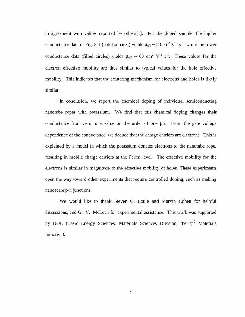
71
in agreement with values reported by others[1]. For the doped sample, the higher
conductance data in Fig. 5-1 (solid squares) yields µeff ~ 20 cm2 V-1 s-1, while the lower
conductance data (filled circles) yields µeff ~ 60 cm2 V-1 s-1. These values for the
electron effective mobility are thus similar to typical values for the hole effective
mobility. This indicates that the scattering mechanism for electrons and holes is likely
similar.
In conclusion, we report the chemical doping of individual semiconducting
nanotube ropes with potassium. We find that this chemical doping changes their
conductance from zero to a value on the order of one µS. From the gate voltage
dependence of the conductance, we deduce that the charge carriers are electrons. This is
explained by a model in which the potassium donates electrons to the nanotube rope,
resulting in mobile charge carriers at the Fermi level. The effective mobility for the
electrons is similar in magnitude to the effective mobility of holes. These experiments
open the way toward other experiments that require controlled doping, such as making
nanoscale p-n junctions.
We would like to thank Steven G. Louie and Marvin Cohen for helpful
discussions, and G. Y. McLean for experimental assistance. This work was supported
by DOE (Basic Energy Sciences, Materials Sciences Division, the sp2 Materials
Initiative).

72
References
This chapter has been submitted to Applied Physics Letters.
1 R. Martel, T. Schmidt, H. R. Shea, et al., Applied Physics Letters 73, 2447
(1998).
2 T. W. Odom, H. Jin-Lin, P. Kim, et al., Nature 391, 62 (1998).
3 J. W. G. Wildoer, L. C. Venema, A. G. Rinzler, et al., Nature 391, 59 (1998).
4 S. J. Tans, R. M. Verschueren, and C. Dekker, Nature 393, 49 (1998).
5 A. M. Rao, P. C. Eklund, S. Bandow, et al., Nature 388, 257 (1997).
6 R. S. Lee, H. J. Kim, J. E. Fischer, et al., Nature 388, 255 (1997).
7 L. Grigorian, G. U. Sumanasekera, A. L. Loper, et al., Phys. Rev. B (Condensed
Matter) 58, R4195 (1998).
8 S. J. Tans, M. H. Devoret, H. Dai, et al., Nature 386, 474 (1997).
9 D. H. Cobden, M. Bockrath, P. L. McEuen, et al., Phys. Rev. Lett. 81, 681
(1998).
10 We note that none of the procedures described hereafter have a significant effect
on metallic tubes, and thus we will focus exclusively on the properties of
semiconducting tubes.
11 We have never seen n-type behavior in undoped samples, even at large positive
gate voltages. We believe that this is because in the back gated geometry the contact
region is screened from the gate by the leads. Thus the contact regions remain p-type
regardless of the gate voltage, preventing the injection of charge into the n-type region.

73
Chapter 6
Disorder, pseudospins, and backscattering in carbon nanotubes
Paul L. McEuen, Marc Bockrath, David H. Cobden*, Young-Gui Yoon, and Steven G.
Louie
Department of Physics, University of California and Materials Sciences Division,
Lawrence Berkeley National Laboratory, Berkeley, California, 94720
Abstract
We address the effects of disorder on the conducting properties of metal and
semiconducting carbon nanotubes. Experimentally, the mean free path is found to be
much larger in metallic tubes than in doped semiconducting tubes. We show that this
result can be understood theoretically if the disorder potential is long-ranged. The effects
of a pseudospin index that describes the internal sublattice structure of the states lead to
a suppression of scattering in metallic tubes, but not in semiconducting tubes. This
conclusion is supported by tight-binding calculations.

74
Single-wall carbon nanotubes (SWNTs) are two-dimensional (2D) graphene
sheets rolled into nanometer-diameter cylinders[1,2] that can either be 1D metals or
semiconductors, depending on how the sheet is rolled up. This surprising behavior
follows from the unusual band structure of a graphene sheet. It is a semimetal with a
vanishing gap at the corners of the first Brillouin Zone (BZ) where the π (bonding) and
π* (antibonding) bands touch at two inequivalent wavevectors K and K’ . (Fig. 6-1A).
As the Fermi level moves due to chemical or electrostatic doping, the Fermi surface
becomes circular arcs at the corners of the BZ, as is shown in Fig. 6-1A for hole doping.
This Fermi surface can be more simply represented in the extended zone scheme by
piecing together the arcs to form Fermi circles of radius k centered around K (K’) point.
When a graphene sheet is rolled up into a tube, the allowed wavevector components
perpendicular to the tube axis become quantized, resulting in 1D subbands with allowed
k’s represented by dashed lines in Figures 6-1B and 6-1C. For metallic tubes (Fig. 6-
1B), one set of allowed wavevectors goes through the K point and there are propagating
modes at Ef at +k and –k. This 1D mode has a linear (massless) dispersion, as is
indicated in the Figure. For semiconducting tubes (Fig. 6-1C), the allowed wavevectors
do not go through the K point. For small k, there are thus no allowed states at Ef, but if
the tube is doped sufficiently, the Fermi circle reaches the nearest 1D subband and
propagating modes exist, whose (massive) dispersion is shown in the Figure.
A wealth of scanned probe and electrical transport measurements have been
performed to probe the electronic structure and conducting properties of SWNTs[2].
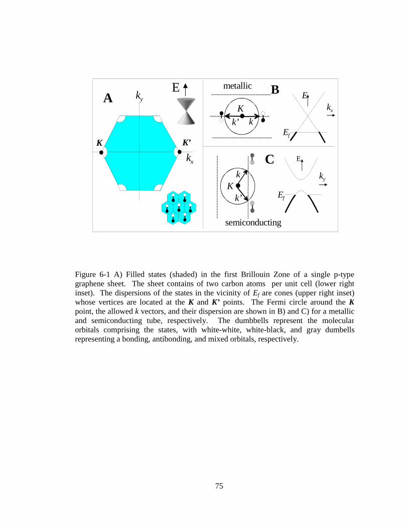
75
kx
ky
K’K
kk’
K
k
k’K
AB
C
E
Ef
Ef
E
E
ky
kx
metallic
semiconducting
Figure 6-1 A) Filled states (shaded) in the first Brillouin Zone of a single p-typegraphene sheet. The sheet contains of two carbon atoms per unit cell (lower rightinset). The dispersions of the states in the vicinity of Ef are cones (upper right inset)whose vertices are located at the K and K’ points. The Fermi circle around the Kpoint, the allowed k vectors, and their dispersion are shown in B) and C) for a metallicand semiconducting tube, respectively. The dumbbells represent the molecularorbitals comprising the states, with white-white, white-black, and gray dumbellsrepresenting a bonding, antibonding, and mixed orbitals, respectively.

76
Overall, the experimental results agree with the predictions of band structure
given above. Many interesting open issues remain, however, particularly concerning the
effect Coulomb interactions[3-6] and disorder[7-9]on the electronic states. For example,
recent theoretical work has emphasized that the effects of disorder may be significantly
reduced in SWNTs for a number of reasons[7-9]. Experiments indeed give compelling
evidence that a metallic tube can have a very long mean free path l - on the order of
microns[10-14] Initial experiments on doped semiconducting tubes, however, have
yielded l ’s that are orders of magnitude shorter[15,16]. This is perhaps surprising,
since the tubes are nearly structurally identical and the amount of disorder likely very
similar. In this letter, we address this apparent discrepancy between the properties of
metallic and doped semiconducting nanotubes.
We begin by discussing the experimental evidence that l can be very long in
metallic SWNTs. Figure 6-2 shows a measurement of a nanotube rope ~ 8µm in length.
At low T, Coulomb oscillations in the conductance G vs. gate voltage Vg are observed as
electrons are added to the rope [10,11]. Using the charging energy U ~ 0.5 meV
determined from the T-dependence, the effective length Leff of the segment of tube to
which the electrons are added can be estimated [10,11]. For this device, we find Leff ~ 10
µm, which is approximately the physical tube length, as previously observed by the
DELFT group[10]. Note that any significant backscattering within the tube would
localize the electronic states on the scale of l and effectively break the tube into a series
of dots[17]. This would result in multiple Coulomb blockade periods as a function of Vg

77
-0.75 -0.70 -0.65 -0.60 -0.550.000
0.050
0.100
0.150
0.200
1.5 K
3 K
T = 5 K
G (
e2 /h)
Vg (V)
VRXUFHGUDLQ
Leff ~ 8 µm
1 µm
Figure 6-2. Conductance versus gate voltage at different temperatures for the metallicnanotube device shown in the upper inset. The 3 nm diameter and 8 µm long nanotuberope is draped over 2 contacts that make tunnel contact to a metallic tube in the rope. Avoltage applied to the doped substrate is used to adjust the carrier density. The appearanceof the CB oscillations only at very low temperatures ( ~1.5 K) indicates that the electronsare delocalized over the entire length of the tube, an indicated in the lower inset.

78
with larger charging energies. The observation of a single, well-defined, and small
charging energy is thus very strong evidence that l is many µms in length.
Additional evidence for large l ’s comes from measurements of the two terminal
conductance of nanotubes with near-ohmic contacts. For perfect contacts, the
conductance is predicted to be: ∑= iTheG )/( 2 , where Ti is the transmission coefficient
for each of the four 1D channels propagating through the tube. Measurements by a
number of groups[11,13,14] have yielded conductances ~ e2/h, indicating that the Ti’s can
be on the order of unity, even for tubes many microns in length. Clearly, then, metallic
tubes can have mean free paths at the micron length scale.
We now turn to experiments on semiconducting tubes. Tans et al.[15] and Martel et
al.[16] measured electrostatically doped p-type tubes and Bockrath et al.[18] measured
n-type tubes that were chemically doped. These results can be analyzed using a model of
a diffusive conductor. In the simplest version, transport though the tube is limited by
scatterers spaced at a distance l, each with transmission probability Ti ~ ½. The
conductance of a tube of length L is then: G ≅ (4e2/h) (l/L). Using the physical length
of the tube and the maximum measured conductance, these experiments indicate l ~
2nm at the largest carrier densities. This is three orders of magnitude shorter than the
l found above for metallic tubes.
To investigate this striking discrepancy further, we have performed extensive
measurements on semiconducting tubes at both room and low temperatures. Figure 6-3
shows the G vs. Vg measured one device. At room temperature, the conductance
increases as Vg is decreased and holes are added to the valence band of the
semiconducting tube. (The saturation of G at large negative Vg is believed to be due to
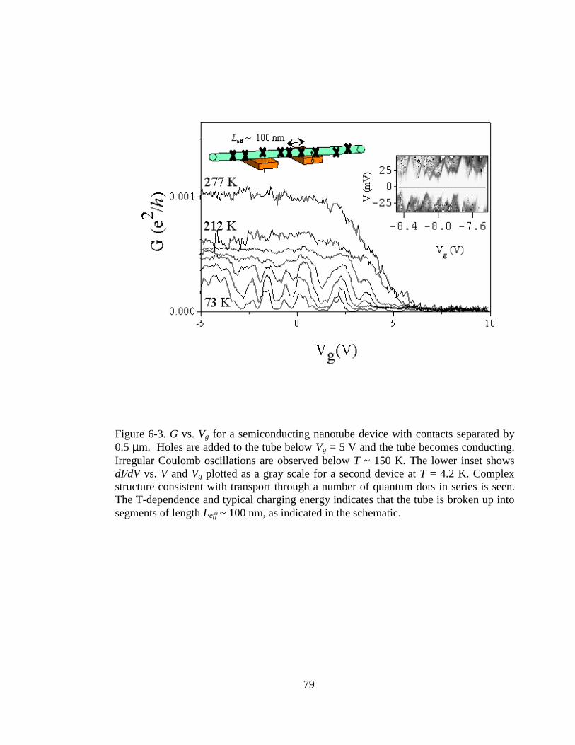
79
Figure 6-3. G vs. Vg for a semiconducting nanotube device with contacts separated by0.5 µm. Holes are added to the tube below Vg = 5 V and the tube becomes conducting.Irregular Coulomb oscillations are observed below T ~ 150 K. The lower inset showsdI/dV vs. V and Vg plotted as a gray scale for a second device at T = 4.2 K. Complexstructure consistent with transport through a number of quantum dots in series is seen.The T-dependence and typical charging energy indicates that the tube is broken up intosegments of length Leff ~ 100 nm, as indicated in the schematic.

80
the contact resistance for tunneling into to the tubes[15,16].) As T is lowered, G is
suppressed and breaks up into a series of peaks as a function of Vg. At low temperatures
(T < 20 K), G is immeasurably small at all Vg. The lower inset to Fig. 6-3 shows the
differential conductance, dI/dV, for a different semiconducting tube device as a function
of Vg and V at T = 4.2 K. The data is plotted as a gray scale. There is a gap around the
origin where dI/dV = 0. This gap shows complex behavior as a function of Vg and is
followed by a finite conductance region above V ~ 25 - 50 mV. Qualitatively similar
results have been obtained on a number of devices consisting of both ropes and single
tubes (as determined by AFM measurements of the rope/tube height).
The data in Fig. 6-3 are highly reminiscent of measurements of the Coulomb
blockade for a number of dots in series[19,20]. In these systems, an electron must hop
through a series of quantum dots, each with a typical charging energy U, for current to
flow. Since at any Vg, some of the dots will be blockaded, dI/dV = 0 at low energies.
Thermal energies kT or finite bias energies eV on the order U are required to overcome
the Coulomb blockade and produce a finite conductance. We therefore conclude that in
semiconducting tubes disorder effectively breaks the tube into a series of dots separated
by tunnel barriers, as is schematically illustrated in the inset to Fig. 6-3. The
conductance is thus determined by tunneling through a series of quantum dots.
We can estimate the size of these disorder-induced dots from the temperature and
bias dependence of the Coulomb blockade features. Since the features appear at energy
scales 100 times larger than for the metallic tube in Fig. 6-2, we find Leff ~ 100 nm.
Since the device is ~ 500 nm long, this implies that the effective sample consists ~ 5 dots

81
in series. From the conductance at room temperature, where charging effects are
minimal, we estimate that the tunnel barriers between the dots each have transmission
probabilites ~ 0.001-0.1.
These measurements indicate that the diffusive transport model discussed
previously – consisting of a large number of scatterers each with Ti ~ ½ - is
inappropriate for these samples. Instead, strong disorder over a much longer length
scale better describes this system. It is still the case, however, that G << e2/h, indicating
that semiconducting tubes are much more strongly influenced by disorder than metallic
tubes.
To understand this difference, we first review in detail the nature of the
electronic states in graphite near Ef. The band structure in the vicinity of the K (K’)
point can be described within the k*p approximation by a 2D Dirac Hamiltonian for
massless fermions, H v kF= ⋅h σ [21]. Here k is the wavevector measured relative to the
K (K’) point and the σ’s are the Pauli matrices. This Hamiltonian is well-known in both
condensed-matter and particle physics; in the latter case, it is used to describe, e.g. a 2D
massless neutrino. The states and their corresponding energies are given by[8,9,21]:
−>=
−⋅
2/
2/
2
1|
k
k
i
irik
e
ibeek θ
θ
; kvbE Fh= (1)
where θ k is the angle that k makes with the y-axis in Fig. 6-1A and b = 1(-1) for states
above(below) the energy at K. Eq. 1 shows that, in addition to their real spin, the
electrons possess a pseudospin - a two-component vector that gives the amplitude of the
electronic wavefunction on the two sublattice atoms. Inspection of Eq. 1 reveals that

82
the spinor is tied to the k vector such that it always points along k. This is completely
analogous the physical spin of a massless neutrino which points along the direction of
propagation. The states around K correspond to right-handed neutrinos (pseudospin
parallel to k), whereas those around K’ are left-handed (pseudospin antiparallel to k).
For the antiparticles (b= -1) this situation is reversed. Physically, this pseudospin means
that the character of the underlying molecular orbital state depends upon the propagation
direction. For example, a negative energy state near K with a positive kx is built from a
anti-bonding molecular orbitals while the state with -kx is built from bonding orbitals.
This is schematically indicated in Fig. 6-1B.
Following Ando and collaborators[8,9], we now consider scattering between
these allowed states in a carbon nanotube due to long-range disorder, i.e. disorder with
Fourier components V(q) such that q << Κ. In this case, the disorder does not couple to
the pseudospin portion of the wavefunction since the disorder potential is approximately
constant on the scale of the inter-atomic distance. The resulting matrix element between
states is then[8]: )(cos|)’(|||)(|’| ’,21222
kkkkVkrVk θ−=>< , where ’,kkθ is the angle
between the initial and final states. The first term is just the Fourier component at the
difference in the k values of the initial and final envelope wavefunctions. The cos term
is the overlap of the initial and final spinor states.
For a metallic tube (Fig. 6-1B), backscattering in the massless subband
corresponds to scattering between |kx >and |-kx >. Such scattering is forbidden,
however, since the molecular orbitals of these two states are orthogonal, as was clearly
emphasized by Ando et al.[8,9]. In semiconducting tubes, however, the situation is quite
different (Fig. 6-1C). The angle between the initial and final states is < π, and scattering

83
is thus only partially suppressed by the spinor overlap. As a result, semiconducting tubes
should be sensitive to long-range disorder, while metallic tubes should not. Note that
short-range disorder, q ~ Κ, will couple the molecular orbitals together and lead to
scattering in all of the subbands.
To support this picture, we have performed tight-binding calculations of the
conductance G of metal and semiconducting tubes in the presence of a scattering
potential. We employ the Landauer formalism to calculate the conductance from the
transmission coefficients Ti of each subband. A Gaussian disorder potential of the form
)2/exp()( 22 σrVrV o −= centered on one of the atoms on the nanotube wall is included in
the tight-binding Hamiltonian. The transmission coefficients are obtained from
boundary condition matching between the disorder-free region and the disordered
region.
In Fig. 6-4, the calculated G(E) is shown for two realizations of a single
Gaussian scatterer with the same integrated strength but different widths corresponding
to long-range (dashed lines) and short-range disorder (dash-dot lines). The massless 1D
band of a metallic tube is unaffected by a long-range scatter, but there is significant
backscattering of the states in the semiconducting tube in the region near the threshold
for transmission. There is also backscattering of the higher subband states of the
metallic tube, as is expected from extending the arguments above. This calculation
clearly demonstrates that the two types of subbands (massive and massless) are affected
very differently by long-range disorder in a manner accurately captured by the physics
of the pseudospin discussed above.

84
Figure 6-4. Tight-binding calculation of the conductance of an A) metallic (10,10)tube and B) semiconducting (17,0) tube in the presence of a Gaussian scatterer. Theenergy scale on the abscissa is 0.2 eV per division in both graphs. The solid linesshow the results for a disorder free tube, while the dash and the dot-dash lines arefor, respectively, a single long-range (σ = 0.348 nm, ∆V = 0.5 eV) and short range (σ= 0.116 nm, ∆V = 10 eV) scatterer centered on the wall of the tube. Here ∆V is theshift in the on-site energy at the potential center. The massless band of the metallictube is unaffected by the long-range scatterer, unlike the massive bands of themetallic and semiconducting tube. All subbands are influenced by the short-rangescatterer. The inset shows an expanded view of the onset of conduction in thesemiconducting tube at positive E, with each division corresponding to 1 meV. Tocompare to the experimental data, we estimate that a gate voltage change Vg of 1 Vin Figure 6-3 corresponds to a chemical potential change E of the on the order of 1meV.

85
These theoretical considerations agree very well with the experimental results. Long-
length scale disorder due to, e.g. localized charges near the tube, breaks the
semiconducting tube into a series of quantum dots with large barriers and a dramatically
reduced conductance. Metallic tubes, on the other hand, are insensitive to this disorder
and remain near-perfect 1D conductors. In the future, it will be great interest to explore
other experimental manifestations of this pseudospin degree of freedom in graphene
materials.
We wish acknowledge useful and enlightening discussions with Dung-Hai Lee
and thank the Smalley group for the nanotube material used in these studies. Y. Yoon
acknowledges discussions with Hyoung Joon Choi and the use of his tight binding code.
This work was supported by DOE, Basic Energy Sciences, Materials Sciences Division,
the sp2 Materials Initiative and by NSF DMR-9520554.

86
References
This chapter has been submitted to Physical Review Letters.
* Present Address: Oersted Laboratory, Neils Bohr Institute, Universitetsparken 5, DK-
2100 Copenhagen, Denmark.
1 M. S. Dresselhaus, G. Dresselhaus, and P. C. Eklund, Science of Fullerines and
Carbon Nanotubes (Academic, San Diego, 1996).
2 For a recent review, see C. Dekker, Physics Today 52, 22 (1999).
3 C. Kane, L. Balents, and M. P. A. Fisher, Phys. Rev. Lett. 79, 5086 (1997).
4 Y. A. Krotov, D.-H. Lee, and S. G. Louie, Phys. Rev. Lett. 78, 4245 (1997).
5 R. Egger and A. O. Gogolin, Phys. Rev. Lett. 79, 5082 (1997).
6 M. Bockrath et al., Nature 397, 598 (1999).
7 C. T. White and T. N. Todorov, Nature 393, 240 (1998).
8 T. Ando, T. Nakanishi, and R. Saito, J. Phys. Soc. Jpn. 67, 2857 (1998).
9 T. Ando and T. Nakanishi, J. Phys. Soc. Jpn. 67, 1704 (1998).
10 S. J. Tans et al., Nature 386, 474 (1997).
11 M. Bockrath et al., Science 275, 1922 (1997).
12 S. Frank et al., Science 280, 1744 (1998).
13 A. Y. Kasumov et al., Science 284, 1508 (1999).
14 H. T. Soh et al., preprint (1999).
15 S. J. Tans, R. M. Verschueren, and C. Dekker, Nature 393, 49 (1998).
16 R. Martel et al., Appl. Phys. Lett. 73, 2447 (1998).
17 A. Bezryadin et al., Phys. Rev. Lett. 80, 4036 (1998).

87
18 M. Bockrath et al., preprint (1999).
19 A. A. M. Staring, H. van Houten, and C. W. J. Beenakker, Phys. Rev. B 45, 9222
(1992).
20 V. Chandrasekhar, Z. Ovadyahu, and R. A. Webb, Phys. Rev. Lett. 67, 2862
(1991).
21 C. L. Kane and E. J. Mele, Phys. Rev. Lett. 78, 1932 (1997).

88
Chapter 7
Electrons in One Dimension: Theory
7.1 Introduction
Interacting electrons in 2- and 3-D are well described in terms of an approximate
model of weakly-interacting quasiparticles, namely Fermi liquid theory. This model has
been highly successful in explaining the properties of 2- and 3-D conductors. However,
this approximate picture does not hold in one dimension. Instead, the ground state of an
interacting 1-D electron gas (I1DEG) is a strongly correlated state known as a Luttinger
liquid. (For review, see e.g.[1].) Unlike in a Fermi liquid, in a Luttinger liquid the low-
energy excitations are bosonic sound-like density waves (plasmons).
One way to observe this Luttinger liquid behavior experimentally is to inject
electrons into a 1-D system from an external lead through a tunneling contact and
measure the resulting current. By varying the energy of the injected electrons, one can
measure the tunneling rates as a function of energy. To first order and at zero
temperature, these tunneling processes are described by:
)()(||2
)( 22
eVEEMh
e
dV
dIeV FsystemFleadtun +== ρρρ , (1)
which relates the tunneling density of states ρtun at a given energy to the product of a
matrix element M and the (joint) density of states ρlead(E1)ρsystem(E2). One usually
neglects both the energy dependence of the matrix element and the energy dependence
of the density of states in the metal lead. For this reason, the differential conductance is

89
often referred to as the “tunneling density of states” of the system being probed by the
leads, although in general the measured dI/dV depends on the tunneling matrix element
as well. In particular, for interacting electrons the dependence of the tunneling rate on
the matrix element may be very important. This is the case in 1-D, where the sudden
creation of an electron in the I1DEG requires the superposition of an infinite number of
plasmons. The resulting orthogonality catastrophe leads to a vanishing of the tunneling
matrix elements near the Fermi level.
Our goal in this chapter is to calculate the tunneling density of states for carbon
nanotubes using a phenomenological model of the Luttinger Liquid. To formulate this
model, we will first find a Lagrangian that describes the low-energy behavior of a non-
interacting 1-D wire with a single spinless mode. From this viewpoint, adding electron-
electron interactions will then become straightforward. Finally, we will consider the
more complicated case of electrons in nanotubes, where there are four conducting modes
at EF.
7.2 Low-energy Lagrangian for a single spinless mode
To find a Lagrangian that describes the low-energy behavior of a 1-D wire, we
will find expressions for the kinetic and the potential energy in terms of a slowly varying
change in the electron density from the ground state. The ground state of the 1-D wire,
taken to have zero total energy, is shown in Figure 7-1A by the solid black lines. The 1-
D momentum states are filled up to the Fermi level EF. To find the potential energy V
per unit length when the charge density is locally increased by an amount ρ, we consider

90
∆ΕF
e∆µ
Figure 7-1A: The local Fermi level of a 1D wire is increased by adding charge (shown in gray).
Figure 7-1B: A current is established by taking left movers in the energy range e∆µ/2 and changing them to right movers

91
adding N electrons to a region of length L>>λF, where λF is the Fermi wavelength. This
results in an increase in the local Fermi level by ∆ΕF, as indicated schematically in
Figure 7-1A by the solid gray lines. The increase in the energy per unit length is
δδ 2
0 4
1
2
11N
Ldnn
LV
N== ∫ (2)
where δ is the level spacing for the right or left movers in a length L:
Lvk
dk
dEF
πδ 2h=∆= . (3)
We arrive at the result
224
ρFve
hV = . (4)
By comparing this with the expression V = ρ2/2κ, where κ is the compressibility of the
non-interacting electron gas[1], we arrive at an expression for the compressibility: κ =
2e2/(hvF).
To find the kinetic energy per unit length T requires an expression for the energy
cost to dynamically change ρ. This energy cost is related to the current in the 1-D wire.
To find this energy, we calculate the increase in energy when a current is established by
taking some left-movers below EF in an energy range of width e∆µ/2 and promoting
them to right-movers above EF. This is shown schematically in Figure 7-1B. The total
energy cost is just the number of electrons N= e∆µ/2δ times the energy added per
electron e∆µ/2. Thus T=( e∆µ/2)2/δ. The difference between the chemical potential of
the right and left movers can be related to the current in the usual way for a 1-D wire:
I=e2/h ∆µ. This leads to the result that

92
224
1I
e
h
vT
F
= . (5)
Since this term goes as the current squared, we define a kinetic inductance L such that
T=1/2 LI2. Thus we find L=h/(2e2vF).
In terms of the kinetic inductance and the compressibility, we find the following
Lagrange density T-V:
22
2
1
2
1 ρκ
−= LIL . (6)
This is the Lagrange density for a transmission line, with the kinetic inductance playing
the role of the usual inductance and the compressibility playing the role of the
capacitance.
Once we have the Lagrangian, we can find the equations of motion for the charge
density. We expect based on the analogy with the transmission line Lagrangian that the
dynamics will be determined by the wave equation. To find these equations in detail, it
is helpful to introduce the displacement θ(x)[1]:
dxtxtxx
),(),( ∫ ∞−= ρθ (7)
Using the continuity equation
x
I
t ∂∂−=
∂∂ρ , (8)
we find
t
txI
∂∂−= ),(θ . (9)
in terms of θ(x,t) the Lagrangian is given by

93
22 )(2
1)(
2
1 θκ
θ xtL ∂−∂=L . (10)
Using the Euler-Lagrange equations
0)()(
=∂∂∂∂+
∂∂∂∂
θθ xx
tt
LL(11)
yields the equation of motion for θ(x,t):
01 22 =∂−∂ θκ
θ xtL (12)
This is the wave equation, which describes waves propagating at the Fermi velocity:
FvL
v ==κ1
. (13)
As mentioned earlier, this is in complete analogy to a transmission line. The velocity
vEM of the electromagnetic wave propagation is given by vEM2=1/LC, where L is the
inductance per unit length and C is the capacitance per unit length.
At this point, this Lagrangian does not give any new information about the non-
interacting 1DEG. It is clear that the excitations in the non-interacting 1DEG should
move at the Fermi velocity. However, from this viewpoint we can account for electron-
electron interactions by adding a term to the Lagrangian arising from the self-
capacitance per unit length C:
2int 2
1 ρC
−=L . (14)
This interaction Lagrangian makes several hidden assumptions that we will discuss later
in the context of discussing electrons in nanotubes. For the time being, we note that the
effect of this term is to add the real capacitance in series with the quantum capacitance
due to the compressibility. The effective capacitance of the I1DEG is then given by

94
κ111 +=
CCeff
. (15)
This leads to an increased wave velocity for the plasmons:
κLLCLCv
effp
111 +== . (16)
The strength of the interactions is characterized by the ratio between the plasmon
velocity and the Fermi velocity and is represented by the interaction parameter g:
2
1
)1(−
+==Cv
vg
p
F κ. (17)
Hence g = 1 characterizes a non-interacting electron gas, while g < 1 for repulsive
interactions.
Finally, we also note that
ppeff
ve
hgLv
C 212
2
1 −== , (18)
which will be useful later.
7.3 Phenomenological Model for Nanotubes
Applying the above theory for a single spinless mode to electrons in carbon
nanotubes is straightforward. The main complication is that a nanotube has four modes
at EF, two channels arising from the electron spin and two channels arising from the
sublattice degeneracy that was discussed in Chapter 1. In the absence of electron-
electron interactions, the Lagrangian is the sum of the single mode Lagrangians[2-4]:
22
2
1
2
1σχσχ
σχρ
κ−= ∑ LIL , (19)

95
Here σ is the electron spin, and χ is an index specifying which sublattice the electron
wavefunction is concentrated on. The electrostatic energy is determined by the total
charge density, and thus the interaction Lagrangian is:
2
int 2
1
−= ∑
σχσχρ
CL . (20)
The appearance of the total charge in the interaction Lagrangian suggests the following
basis[2, 4]:
The sum of the spin density on the two sublattices (denoted by a and b,)
)(2
1bbaas ↓↑↓↑+ −+−= ρρρρρ , (21)
the difference in spin density on the two sublattices,
)(2
1bbaas ↓↑↓↑− +−−= ρρρρρ , (22)
the total charge density,
)(2
1bbaac ↓↑↓↑+ +++= ρρρρρ , (23)
and the difference in the charge on the two sublattices
)(2
1bbaac ↓↑↓↑− −−+= ρρρρρ . (24)
Three of these modes are neutral, and one is charged. Note that because of the
normalization factors involved in the change of basis, the charge carried by the charged
mode is ½ of the physical charge. In this new basis the Lagrangian is given by
222222222 2)(
2
1)(
2
1+−+−+−+−+ −+++−+++= cccssccss C
IIIIL ρρρρρκ
L . (25)

96
Hence, these modes behave like four independent spinless 1-D modes. Interactions
affect only the charged mode, which has a plasmon velocity given by
κLLCv p
14 += . (26)
This gives the following value for gc+:
2
1
)4
1(−
+ +==Cv
vg
p
Fc
κ, (27)
While the g = 1 for the three neutral modes. We see that the addition of more modes
results in a lower value for gc+ compared to a single mode. For a finite size system of
length l, Eq. 27 can be written in terms of the mean level spacing ∆ = hvF/4l, and the
charging energy U = e2/Ctot, where Ctot is the total capacitance:
2
1
)2
1(−
+ ∆+= U
gc . (28)
This expression is useful for direct comparison of theory and experiment.
As mentioned previously, the interaction Lagrangian given by Eq. 20 makes
several assumptions. The first is that there is in fact a well-defined capacitance per unit
length. As is known from elementary electrostatics, the capacitance per unit length C of
a wire of radius R and length l approaches zero as
)/ln(
2 0
RlC
πε= . (29)
Hence, in order for a local capacitance to be defined that is independent of l, the length
of the wire must be greater than the screening length ls, which is some long distance cut-
off for the Coulomb interaction. In this case, C is independent of the length and is given
by
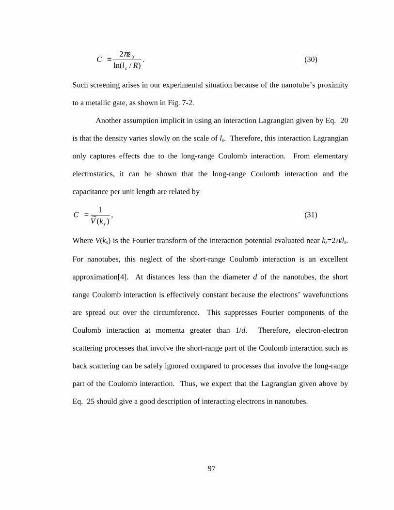
97
)/ln(
2 0
RlC
s
πε= . (30)
Such screening arises in our experimental situation because of the nanotube’s proximity
to a metallic gate, as shown in Fig. 7-2.
Another assumption implicit in using an interaction Lagrangian given by Eq. 20
is that the density varies slowly on the scale of ls. Therefore, this interaction Lagrangian
only captures effects due to the long-range Coulomb interaction. From elementary
electrostatics, it can be shown that the long-range Coulomb interaction and the
capacitance per unit length are related by
)(~
1
skVC = , (31)
Where V(ks) is the Fourier transform of the interaction potential evaluated near ks=2π/ls.
For nanotubes, this neglect of the short-range Coulomb interaction is an excellent
approximation[4]. At distances less than the diameter d of the nanotubes, the short
range Coulomb interaction is effectively constant because the electrons’ wavefunctions
are spread out over the circumference. This suppresses Fourier components of the
Coulomb interaction at momenta greater than 1/d. Therefore, electron-electron
scattering processes that involve the short-range part of the Coulomb interaction such as
back scattering can be safely ignored compared to processes that involve the long-range
part of the Coulomb interaction. Thus, we expect that the Lagrangian given above by
Eq. 25 should give a good description of interacting electrons in nanotubes.

98
d
Figure 7-2: A carbon nanotube a distance d above a conducting plane. The presense of the conducting plane cuts off the long-range Coulomb interaction for distances greater than the screening length ls = 2d.

99
7.4 Tunneling Density of States and the Semiclassical Approximation
With our faith in the simplified model confirmed, we can proceed to compute the
tunneling density of states. In general, this is given by the expression
)(|0|)(||2)( 02 EEExnE n
ntun −−><= ∑ + δψπρ , (32)
where |n> are the exact eigenstates of the Hamiltonian and En are the energy
eigenvalues, and Ψ(x) is the electron annihilation operator. Using the identity
dteEEE tEEEin
n∫∞ −+=−−
0
/)(0
01
)( h
hπδ , (33)
yields the result
dtxtxeE iEt∫∞ + ><=
0
/ 0|)0,(),(|0Re1
)( ψψπ
ρ h
h. (34)
The density of states is therefore related to the Fourier transform of the electron Green’s
function,
>=< + 0|)0,()’,’(|0)’,’,( xtxtxxG ψψ , (35)
evaluated at x = x’. This is the amplitude to introduce an electron into the system at t = 0
at x, and find it again at x at a later time t = t’. We will avoid the difficulties associated
with quantum theory by utilizing the semiclassical approximation to compute the
electron Green’s function, which we will now briefly review (see e.g. [5].)
In general, the amplitude for a quantum system to make a transition between any
two states can be calculated by summing the exponential of the classical action over all
paths connecting the initial and final states. Explicitly, this reads
DxdtLi
xtxtxxGt
cl∫∫>==< +
0
’
paths
)exp(0|)0,(),’(|0),’,(h
ψψ . (36)
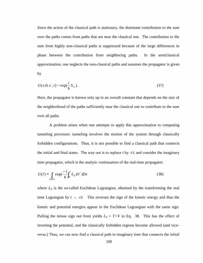
100
Since the action of the classical path is stationary, the dominant contribution to the sum
over the paths comes from paths that are near the classical one. The contribution to the
sum from highly non-classical paths is suppressed because of the large differences in
phase between the contribution from neighboring paths. In the semiclassical
approximation, one neglects the non-classical paths and assumes the propagator is given
by
)exp(~),;0,( ’clS
itxxG
h. (37)
Here, the propagator is known only up to an overall constant that depends on the size of
the neighborhood of the paths sufficiently near the classical one to contribute to the sum
over all paths.
A problem arises when one attempts to apply this approximation to computing
tunneling processes: tunneling involves the motion of the system through classically
forbidden configurations. Thus, it is not possible to find a classical path that connects
the initial and final states. The way out is to replace t by -iτ, and consider the imaginary
time propagator, which is the analytic continuation of the real-time propagator:
DxdLG E∫∫−=
τττ
0
’
paths
)1
exp()(h
(38)
where LE is the so-called Euclidean Lagrangian, obtained by the transforming the real
time Lagrangian by t → -iτ. This reverses the sign of the kinetic energy and thus the
kinetic and potential energies appear in the Euclidean Lagrangian with the same sign.
Pulling the minus sign out front yields LE = T+V in Eq. 38. This has the effect of
inverting the potential, and the classically forbidden regions become allowed (and vice-
versa.) Thus, we can now find a classical path in imaginary time that connects the initial

101
and final states. The imaginary time propagator in the semiclassical approximation
becomes
)1
exp(~)( clSGh
−τ . (39)
Note that the transition amplitude decays exponentially with the action, which is the
behavior one usually expects for tunneling through a classically forbidden configuration.
In contrast with the real time formalism, the principle of least action is enforced by
cutting off the non-classical paths by an exponentially small factor, rather than by
canceling the contributions of neighboring paths by virtue of their rapidly varying phase.
7.5 Tunneling into a Nanotube
To compute the tunneling density of states, we now introduce a model for
tunneling given in Fisher and Glazman[1]. In this model, the Luttinger liquid is
interrupted by a barrier, as shown in Fig. 7-3. Tunneling proceeds through the barrier in
a fast step that results in the sudden creation of a localized electron on the right hand
side of the barrier. (This process leads to an overall pre-factor in the tunneling rate and
we will neglect it in what follows.) However, at zero energy, the resulting configuration
is classically forbidden. The tunneling process then proceeds by a slow phase in which
the charge density relaxes to the ground state. Since the configuration is classically
forbidden at all times during tunneling, we will use the imaginary time propagator to
compute the Green’s function. Also, as discussed previously, we will compute the
Green’s function using the semiclassical approximation[1]. By considering the action
due to the charge relaxation on one side of the barrier only, we will compute the

102
Figure 7-3: Luttinger liquid interrupted by a barrier, producing two tunnel-coupled half-infinte Luttinger liquids. The diagram depicts a tunneling process in which an electron is removed from the Luttinger liquid on the left, leaving a hole, and is added to the Luttinger liquid on the right.

103
tunneling density of states for adding an electron to the end of a single half-infinite
Luttinger liquid.
To use this model for tunneling into a nanotube, we consider the creation of a
localized electron in a specific mode, say ρ↑a. (The result is independent of the specific
chosen mode.) This initial state requires the excitation all four of the modes ρc+, ρc-, ρs+,
ρs-, and hence the initial conditions read:
)()(22
1xexesscc δδρρρρ ===== −+−+ , (40)
where the ½ comes from the normalization factor and the two comes from the fact that
the density is only nonzero to the right of the barrier. The final state is given by
0==== −+−+ sscc ρρρρ . (41)
Now we must find the classical path that connects the initial state to the final
state. The equations of motion are the imaginary-time wave equation (ITWE.) For the
four modes, these read
0,/22
,/,/2 =∂+∂ ±±± scxscsct v θθ . (42)
with vc/s,+ being either the Fermi velocity or the plasmon velocity as appropriate. Note
that this differs from the usual wave equation by a change of sign. The general solution
of this equation is
)()( ,/,/,/ ττθ ±±± −++= scscsc ivxgivxf , (43)
where g(x) and f(x) are arbitrary functions describing right and left propagating waves.
This form, while very general, is somewhat difficult to match to the initial condition
where θ(x,0) is proportional to the unit step function. There are many ways to proceed.

104
One way is motivated by the fact that the solution must connect a delta function density
at t = 0 to zero density at t → ∞. Thus, we try to find a solution that spreads out,
=
τθ
v
xu , (44)
where u is an unknown function for which to solve. Putting this trial function into the
ITWE yields the ordinary differential equation
02)1( 2 =++ uu &&& ηη , (45)
where η = x/vτ. This equation is readily solved by integration to yield
21
1 tan CCu += − η where C1 and C2 are constants of integration. Note that this is a
special case of Eq. 43 since
[ ]iivxivxi
v
x πτττ
−+−−−=
− )ln()ln(
2tan 1 . (46)
It is straightforward to verify that
=
±
−± τπ
θ,/
1,/ tan
scsc v
xe(47)
matches the initial conditions given by Eq. 40 and solves the ITWE. The density is then
2,/
2,/
,/ )(),(
ττ
πρ
±
±± +
=sc
scsc vx
vetx . (48)
This function is plotted in Fig. 7-4A and Fig. 7-4B.
Now that we have determined the classical path, we can determine the action of
the classical path. This requires us to integrate the Lagrange density over space and
time. As discussed previously, in imaginary time the Lagrange density is the sum of the
potential and kinetic energies, rather than the difference. Therefore, the action will be
the sum of the action due to the potential energy and the action due to the kinetic energy.
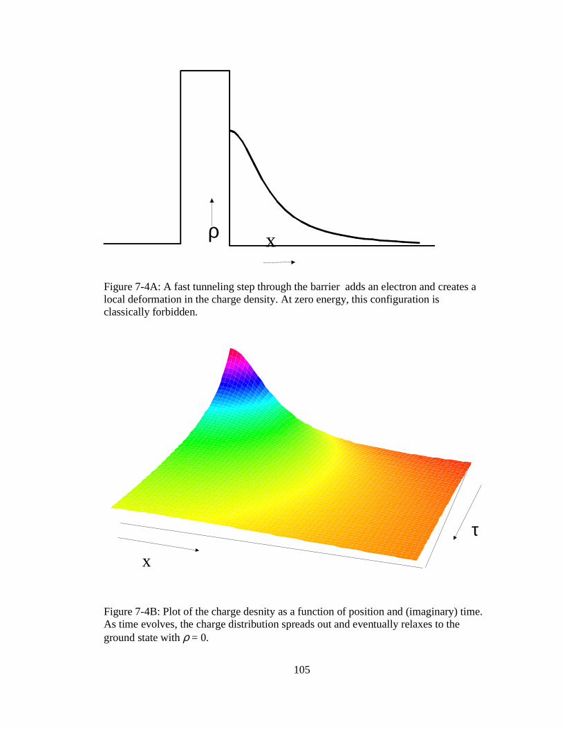
105
x
τ
xρ
Figure 7-4A: A fast tunneling step through the barrier adds an electron and creates a local deformation in the charge density. At zero energy, this configuration is classically forbidden.
Figure 7-4B: Plot of the charge desnity as a function of position and (imaginary) time. As time evolves, the charge distribution spreads out and eventually relaxes to the ground state with ρ = 0.

106
The potential energy due to the deformation caused by the tunneling electron is the sum
of the potential energies from each mode and is given by
dxvx
vv
e
hg
eV
sc sc
scscscdef
2
,/0 2
,/2
,/,/2
1,/2
2
)(22)( ∑ ∫
±
∞
±
±±
−±
+=
τ
τ
πτ
dxvx
vvg
h
sc sc
scscsc
2
,/0 2
,/2
,/,/
1,/2 )(4
∑ ∫±
∞
±
±±
−±
+=
τ
τ
π
( )316
1 += −+cg
h
πτ. (49)
Physically, this 1/τ dependence arises because the density ρ goes as 1/τ while the width
W of the density packet goes as τ. Hence the Vdef ~ ρ2W ~ 1/τ. Considering zero total
energy, the kinetic energy is equal to the potential energy and thus the action is
’)’(2)(/
ττττ
dVScE def∫=
h
(50)
h
τπ
cc
Eg
hln)3(
81 += −+ . (51)
Here, Ec is a high energy cut off on the order of e2/a, where a is the typical electron
spacing, or any other short range cutoff to the Coulomb interaction, e.g. the tube
diameter. The imaginary time propagator is then given by
βτττ−
=−
hh cE
SG )/)(exp(~)( , (52)
with β = (gc+ -1+3)/4. Hence, the exponential decay normally associated with tunneling
through a classically forbidden configuration is cancelled by the logarithmic divergence
of the action, resulting in power law behavior.
107
To arrive at the tunneling density of states we analytically continue the
imaginary time propagator back to real time and compute the Fourier transform:
dttiE
eE ciEttun ∫
∞−
0
/Re1
~)(β
πρ
hhh (53)
The behavior with respect to energy can be determined via a change of variables u =
2πEt/h (E>0). The integral then becomes
( ) duuiEeE
E ciu
tun ∫∞ −
0Re~)( β
α
πρ , (54)
where
α = αend = β−1 = (gc+ -1-1)/4. (55)
This implies that the differential conductance dI/dV ~ Vα, and the conductance G ~ Tα.
Note that for arbitrarily weak interactions (for any gc+ < 1) the tunneling density of
states vanishes at zero energy. This behavior is very different from that of the non-
interacting 1DEG, where for energies near the Fermi level the tunneling density of states
is constant. This is an essential distinction between the I1DEG and the non-interacting
1DEG.
Finally, this analysis is appropriate for determining the tunneling density of
states when the electron tunnels into the end of the nanotube. If the electron tunnels into
the middle, or bulk, the electron can spread out in two directions rather then one. As the
electron spreads out, the charge density is half as much but spread out over twice the
length as compared to the end tunneling case. Since the action is quadratic in the charge
density but linear in the size of the charge packet, the action for tunneling into the
middle is half the action for tunneling into the end. Hence, we expect that the tunneling
exponent for tunneling into the middle should be approximately half of the exponent for

108
tunneling into the end. A more detailed calculation[2, 4] yields the result ρ(E) ~ Eα,
where
α = αbulk = (gc+ -1+ gc+-2)/8. (56)
For g<<1 where it is expected that semiclassical reasoning is most valid, αbulk indeed
approaches ½ the value of the αend.
7.6 Limit of Many Modes and Connection to Coulomb Blockade Model
The above model for nanotubes with four conducting modes at EF can be
extended to the general case of N conducting modes at EF[6]. The Hamiltonian for an N
mode wire is given by
2
22
2
1
2
1
2
1H
++= ∑∑
nnnn
n CLI ρρ
κ, (57)
Where ρn is the density of charge in the nth mode, and In is the corresponding current.
Here as before, the interaction term depends only on the total charge. With a change of
variables via a rotation to basis in which one mode is the total charge and the rest are
orthogonal to this mode, this becomes
∑−=
=+++ ++++=
1
1
20
20
222
2
1
2
1
22
1
2
1H
Nn
nncncccc LI
C
NLI ρ
κρρ
κ, (58)
where ρc+ is the charged mode, Ic+ the corresponding current, ρc0n the nth neutral mode,
and Ic0n the nth neutral current. Note that because the change in variables used here is an
orthonormal transformation, the physical charge is related to the ρc+ by ρphysical = N1/2
ρc+. The sum in the Eq. 58 runs over the N-1 neutral modes. In this basis, the N modes

109
behave independently. The interaction strength g can be computed for each mode. The
result is that
2
1
)1(−
+ +==C
N
v
vg
p
Fc
κ(59)
for the charged mode, and gc0n = 1 for the N-1 neutral modes.
The tunneling density of states can be calculated using the same method
employed in the previous section with the result that αend = (gc+ -1-1)/N. In the limit
where N>>1, gc+ ~ (1/N)1/2. Thus we have α ∼ (1/N)1/2 to leading order. Hence as the
number of modes tends to infinity, the behavior of the wire tends toward the non-
interacting result α = 0. Physically, this occurs because in the limit N>>1, the tunneling
action is dominated by the spreading out of the neutral modes, and the contribution from
the charged mode becomes comparatively negligible. The result is that the tunneling
density of states is thereby determined by the non-interacting neutral modes, which gives
rise to the ohmic behavior expected for tunneling into a system of non-interacting
electrons.
Finally, we note the connection between this theory and the theory of Coulomb
blockade of tunneling in a resistively isolated tunnel junction (CB theory). (For review,
see e.g. [7]). In the CB theory at low energies the tunneling rate goes as a power law in
the applied bias,
αVdV
dI~ , (60)
where the exponent α is determined by the isolating impedance Z:
Zh
e22=α . (61)

110
As we will now show, this model is equivalent to the model discussed earlier in the limit
of many modes. In that model, α is given by:
−
+=
−
+=
−=
+
111
111
111
2/1
2
2/1
Fc LCv
N
NC
N
NgN
κα (62)
In the limit that N>>1, to leading order
NC
L
h
e
NLCvNC F
2211 === κα . (63)
This agrees with Eq. 61 provided the characteristic impedance of a multi-mode wire is
given by Z = (L/NC)1/2 in the limit where N>>1. To show this, we note that only the
charged mode couples to an external electric field[8]. Hence the impedance of the
neutral modes is infinite and the impedance of the wire is determined solely by the finite
impedance of the charged mode. The Hamiltonian for the charged mode may be written
in terms of the physical charge ρ = Ν1/2 ρc+, and the corresponding current I. The result
is
22
2
1
2
1
2
1H ρ
κ
++=
CNLI
N. (64)
In an ordinary electromagnetic transmission line with capacitance per unit length C0 and
inductance per unit length L0, the characteristic impedance Z0 is given by Z0 = (L0/C0)1/2.
By analogy, the characteristic impedance Z of the multi-mode wire is given by
+=
κNCN
LZ
2
11. (65)
In the limit N>>1, to leading order in N, this approaches
NC
LZ = , (66)

111
and thus the theory given by Eq. 57 reproduces the results of the CB theory in the limit
where N>>1.
112
7.7 Summary
In conclusion, we have presented a simplified phenomenological model for a
I1DEG and applied it to computing the tunneling density of states of metallic carbon
nanotubes. This tunneling density of states shows power law behavior with an exponent
that depends on whether the electron tunnels into the end of the nanotube or into the
middle. In particular, ρ(E) ~ Eα, where α = (gc+ -1-1)/4 in the case of tunneling into the
end, and α = αbulk = (gc+ -1+ gc+-2)/8 in the case of tunneling into the middle. This
power-law vanishing of the tunneling density of states at low energies is a striking
feature that signifies the correlated nature of the I1DEG.

113
References
1 M. P. A. Fisher and L. I. Glazman, in Mesoscopic electron transport, edited by
L. L. Sohn, L. P. Kouwenhoven and G. Schoen (Kluwer Academic Publishers,
Dordrecht ; Boston, 1997).
2 R. Egger and A. O. Gogolin, Phys. Rev. Lett. 79, 5082 (1997).
3 R. Egger and A. O. Gogolin, European Physical Journal B 3, 281 (1998).
4 C. Kane, L. Balents, and M. P. A. Fisher, Phys. Rev. Lett. 79, 5086 (1997).
5 R. Shankar, Principles of Quantum Mechanics (Plenum, New York, 1994).
6 K. A. Matveev and L. I. Glazman, Phys. Rev. Lett. 70, 990 (1993).
7 G.-L. Ingold and Yu. V. Nazarov, in Single charge tunneling: Coulomb blockade
phenomena in nanostructures, edited by H. Grabert and M. H. Devoret (Plenum Press,,
New York :, 1992).
8 K. A. Matveev and L. I. Glazman, Physica B 189, 266 (1993).
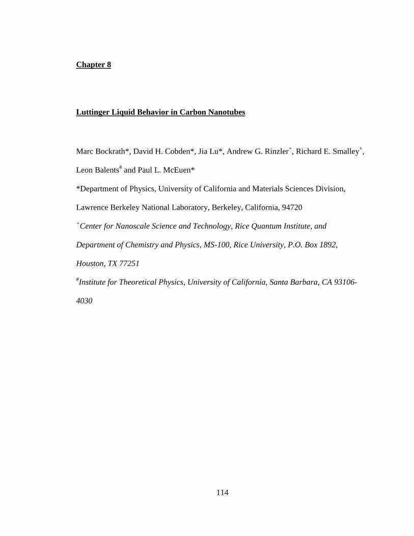
114
Chapter 8
Luttinger Liquid Behavior in Carbon Nanotubes
Marc Bockrath*, David H. Cobden*, Jia Lu*, Andrew G. Rinzler+, Richard E. Smalley+,
Leon Balents# and Paul L. McEuen*
*Department of Physics, University of California and Materials Sciences Division,
Lawrence Berkeley National Laboratory, Berkeley, California, 94720
+Center for Nanoscale Science and Technology, Rice Quantum Institute, and
Department of Chemistry and Physics, MS-100, Rice University, P.O. Box 1892,
Houston, TX 77251
#Institute for Theoretical Physics, University of California, Santa Barbara, CA 93106-
4030

115
Electron transport in conductors is usually well described by Fermi-liquid theory,
which assumes that the energy states of the electrons near the Fermi level EF are not
qualitatively altered by Coulomb interactions. In one-dimensional systems, however,
even weak Coulomb interactions cause strong perturbations. The resulting system,
known as a Luttinger liquid, is predicted to be distinctly different from its two- and
three-dimensional counterparts[1]. For example, tunneling in to a Luttinger liquid at
energies near the Fermi level is predicted to be strongly suppressed, unlike in two- and
three-dimensional metals. Experiments on one-dimensional semiconductor wires[2,3]
have been interpreted using Luttinger-liquid theory, but an unequivocal verification of
the theoretical predictions has not yet been obtained. Behavior consistent with a chiral
Luttinger liquid has been observed in fractional quantum Hall conductors[4-6], although
questions remain about the connection between theory and experiment. Electrically
conducting single-walled carbon nanotubes (SWNTs) represent quantum wires[7-10]
that may exhibit Luttinger-liquid behavior[11,12]. Here we present measurements of the
conductance of bundles (‘ropes’) of SWNTs as a function of temperature and voltage
that agree with predictions for tunneling into a Luttinger liquid. In particular, we find
that the conductance and differential conductance scale as power laws with respect to
temperature and bias voltage, respectively, and that the functional forms and the
exponents are in good agreement with theoretical predictions.
Since the initial discovery of SWNTs, experiments have revealed a great deal
about their electronic properties. STM measurements of individual tubes have verified
that they are either 1D semiconductors or conductors, depending upon their
chirality[7,8]. Electrodes have also been attached to nanotubes and ropes of nanotubes

116
to probe transport. These electrodes make tunneling contacts to the tubes and, for
conducting tubes, the resulting structure behaves as a 1D quantum dot. It was found that
for ropes transport was typically dominated by a single nanotube in the rope[9]. This is
reasonable since the majority of the tubes comprising a rope are insulating at low
temperatures[7,8] Measurements of such devices have been used to study the charging
energy, level spacing, and spin state of a nanotube[9,10,13,14].
The devices used in these previous experiments had two distinct geometries, one
which contacted the ends of a tube and one which contacted the bulk, as is discussed in
the legend to Fig. 1. Here, we explore the transport properties of rope samples in both of
the geometries. Fig. 1 shows the linear-response two-terminal conductance, G, versus
gate voltage, Vg, for a bulk-contacted metallic rope. At low temperatures, it exhibits a
series of Coulomb oscillations[15] that occur each time that an electron is added to a
nanotube within the rope. From the temperature dependence, we find that the charging
energy U for this sample is 1.9 meV. For kBT > U (i.e. T > 20 K), the Coulomb
oscillations are nearly completely washed out, and the conductance is independent of
gate voltage. A plot of the conductance vs. temperature in this regime is shown in the
inset. The conductance drops steeply as the temperature is lowered, extrapolating to G =
0 at T = 0.
Results for a number of samples are shown in Fig. 2, where the G versus T is
plotted on a log-log scale (solid lines). Fig. 2(a) shows data for end-contacted ropes,
whereas Fig. 2(b) shows the data for bulk-contacted ropes. The measured data (solid
lines) shows approximate power law behavior for the four samples shown. However, the
range of temperature over which the power law behavior occurs is limited by the effects

117
0.0 0.9 1.8 2.7 3.60
5
10
15
20
285 K
129 K
40 K
1.3 K
16 K
8 K
G (
µS)
Vg (V)
0 100 200 3000
5
10
15
20
T (K)
G (
µS)
Figure 8-1: The two-terminal linear-response conductance G vs. gate voltage Vg for abulk-contacted metallic rope at a variety of temperatures. The data show significanttemperature dependence for energy scales above the charging energy that cannot beexplained by the Coulomb blockade model. Inset: Average conductance plotted as afunction of temperature T. The devices used in these experiments are made in one oftwo ways. In both methods, SWNTs are deposited from a suspension indichloroethane onto 1-µm thick SiO2 that has been thermally grown on adegenerately doped Si wafer. The degenerately doped silicon substrate is used as agate electrode. AFM imaging reveals that the diameter of the ropes vary between 1and 10 nm. In the first method[9], chromium-gold contacts are applied over the topof the nanotube rope using electron beam lithography and lift-off. Frommeasurements of these devices in the Coulomb blockade regime, we conclude thatthe electrons are confined to the length of rope between the leads. This implies thatthe leads cut the nanotubes into segments, and transport involves tunneling into theends of the nanotubes (“end-contacted”). In the second method[10], electron beamlithography is first used to define leads, and ropes are deposited on top of the leads.Samples were selected that showed Coulomb blockade behavior at low temperatureswith a single well-defined period, indicating the presence of a single dot. Thecharging energy of these samples indicates a dot with a size substantially larger thanthe spacing between the leads, as found by Tans, et al.[10] Transport thus occurs byelectrons tunneling into the middle, or bulk, of the nanotubes (“bulk-contacted”).
118
10 1001
10
G(µ
S)
T(K)10 100
1
10
T(K)
0.0 0.2 0.4 0.6 0.8 1.0α
b)a)
Figure 8-2: Conductance G plotted against temperature T for individualnanotube ropes. The data are plotted on a log-log scale. Figure 2a shows datafor ropes that are deposited over pre-defined leads (bulk-contacted), whereasFig. 2b shows the data for ropes that are contacted by evaporating the leads ontop of the ropes (end-contacted). Sketches depicting the measurementconfiguration are shown in the lower right insets. The plots show both the baredata (solid line) and the data corrected for the temperature dependence expectedfrom the Coulomb blockade (CB) model (dashed line). We correct the data bydividing the measured G(T) by the theoretically expected temperaturedependence in the CB model. This correction factor only depends upon U/kBT,and, since U can be independently measured from the temperature dependenceof the Coulomb oscillations, the correction procedure requires no adjustableparameters. If the CB were the only source of the temperature dependence, thedashed lines would be horizontal. Instead they have a finite slope, indicating anapproximate power-law dependence on T. The upper left inset to Figure 2(a)shows the power-law exponents inferred for a variety of samples. Open circlesdenote end-contacted devices, while crosses denote bulk-contacted ones.

119
of Coulomb blockade at low temperatures. After correcting for the known temperature
dependence due to the Coulomb blockade[15], the corrected data (dashed lines) shows
power law behavior over a greater range, with slightly different exponents. Above
T~100 K, G begins to saturate for some samples. This saturation is observed in many,
but not all, of the samples studied.
Focusing on the corrected data, the bulk-contacted samples show approximate
power law behavior from 8 – 300 K with exponents αbulk ≈ 0.33 and 0.38. The end-
contacted samples show approximate power law behavior from 10 - 100 K with
exponents αend ≈ 0.6 for both samples. The upper inset to Fig. 2(a) shows the exponents
determined from the temperature dependence for a variety of samples. Exponents
marked with an ‘x‘ and ‘o’ are for bulk- and end- contacted tubes, respectively. The
bulk-contacted samples show a systematically lower exponent than end-contacted
devices, with αend ~ 0.6 and αbulk ~ 0.3.
Figure 3 shows the measured differential conductance dI/dV of these devices as a
function of the applied bias V. The upper left inset to Fig. 3(a) shows results for a bulk-
contacted device at different temperatures, plotted on a log-log scale. At low biases,
dI/dV is proportional to a (temperature-dependent) constant – G(T) from Figure 2. At
high biases dI/dV increases with increasing V. The curves at different temperatures fall
onto a single curve in the high bias regime. Since this curve is roughly linear on a log-
log plot, it implies that the differential conductance is described by a power law, dI/dV ~
Vα, where α = 0.36. At the lowest temperature T=1.6 K, this power law behavior occurs
over two decades in V, from 1 mV < V < 100 mV.

120
100 101
10-1
100
T=20 K T=40 K T=67 K
b)a)
Sca
led
Con
duct
ance
eV/kT10-210-1100 101 102 103
100
101
T=1.5 K T=8 K T=20 K T=35 K
eV/kT
10-1 100 101 102100
101
dI/d
V (
µS)
V (mV)100 101 102100
101
dI/d
V (
µS)
V (mV)
Figure 8-3: The differential conductance dI/dV measured at varioustemperatures. Figure 3a inset: dI/dV curves taken on a bulk-contacted rope attemperatures T=1.6 K, 8 K, 20 K, and 35K. Figure 3b inset: dI/dV curves takenon an end-contacted rope at temperatures T=20 K, 40 K, and 67K. In bothinsets, a straight line on the log-log plot is shown as a guide to the eye toindicate power-law behavior. The main panels show these measurementscollapsed onto a single curve using the scaling relations described in the text.The solid line is the theoretical result fit to the data using γ as a fittingparameter. The values of γ resulting in the best fit to the data are γ = 0.46 in (a)and γ = 0.63 in (b).
121
The upper left inset to Fig. 3(b) shows dI/dV as a function of V for an end-
contacted sample at several temperatures. The conductance is again a temperature-
dependent constant at low biases eV << kBT, whereas at higher biases dI/dV increases.
The high bias data follows an approximate power law before rolling off to reduced slope
for V > 30 mV. While the range of data is too small to conclude that a power law
accurately describes the behavior at intermediate voltages, if a straight line is fit to the
range 9 mV< V < 32 mV the exponent obtained is α = 0.87.
We now discuss the possible origins this approximate power law behavior. One
possible explanation is that the tunnel barriers are strongly energy-dependent, with
increased transparency at high energies. This would lead, e.g. to activated transport:
G~exp(-∆/kBT) over the barrier. However, the fact that the temperature dependence
extrapolates to G = 0 at T = 0 (Figure 1 inset) is inconsistent with this functional form.
Another potential explanation is that transport occurs through multiple dots in
series formed by disorder[16] or by barriers produced when the nanotubes bend over the
lithographically defined contacts[17]. We rule this possibility out however, as we have
chosen to study only samples where a single dominant period for the Coulomb
oscillations is observed at low temperatures. This indicates the existence of only a single
dot.
Having excluded these possibilities, let us consider whether the behavior can be
explained by the predictions of Luttinger Liquid (LL) theory. A LL is a one-
dimensional correlated electron state characterized by a parameter g that measures the
strength of the interaction between electrons. For any g ≠ 1, the low energy excitations

122
of the system are not all weakly interacting quasiparticles, and the Fermi liquid theory
used to describe conventional metals is not appropriate.
In SWNTs, the long-range Coulomb interaction between electrons is expected to
yield an LL with g < 1[11,12] For a finite length tube or rope, the Luttinger parameter g
is given by:
(1)
where U = e2/C is the charging energy of the tube and ∆ = π h vF/2L is the single-
particle level spacing (the two 1D subbands of the nanotube are assumed to be non-
degenerate). From previous measurements and theoretical estimates[9,10] U/∆ ~ 6.,
yielding an expected Luttinger parameter g(theory) ~ 0.28.
Tunneling of an electron into a LL is dramatically different than tunneling into
Fermi liquid. For a Fermi liquid, an energy-independent tunneling amplitude is
expected for energies near EF, where EF is the Fermi level. This yields a temperature-
and bias-independent tunneling conductance. For a clean LL on the other hand, the
tunneling amplitude is predicted to vanish as a power law in E-EF. This leads to a
power-law variation of G with T at small biases (eV<< kBT):
G(T) ~ ATα (2)
or with V at large biases (eV >>kBT) :
dI/dV ~Vα (3).
2/1]2
1[ −∆
+= Ug

123
The exponent of these power laws depends on the number of 1D channels[18] and
whether the electron tunnels into the bulk or the end of the LL. For a SWNT with four
conducting modes at EF, the exponents are[11,12]:
αend = (g-1 - 1) / 4 (4a)
αbulk = (g-1 + g - 2) / 8. (4b)
Using equations 1 and 4, we obtain αend(theory) = 0.65 and αbulk(theory) = 0.24.
To compare the theoretical predictions for tunneling into an isolated nanotube
through a single barrier to the experimental geometry where ropes are connected by two
contacts, we must make two assumptions. First, we assume that transport in the rope is
dominated by a single metallic tube, as discussed previously. Preliminary theoretical
studies of ropes composed of SWNTs with a relatively small fraction of metallic tubes
support this assumption. These studies find that the only significant inter-tube coupling
is electrostatic. Such an interaction will introduce extra screening of the Coulomb
interaction but, because of the weak (logarithmic) dependence of g on the screening
length, the LL predictions are essentially unchanged. Second, we assume that the tunnel
resistances into and out of the tube are the dominant resistances in the system. The
circuit thus consists of two tunnel junctions in series, with the current response of each
junction is described by equations 1-4. Note that the voltage drop across the highest
impedance junction will be some fraction γ of the total applied bias V, where 1/2 ≤ γ ≤
1. If the barriers are equal, the voltage will divide equally between these junctions and γ
= 1/2. Alternately, if the resistance of one junction dominates, γ = 1.
With these assumptions, the approximate power law behavior as a function of T
or V observed in Figures 2 and 3 then follows from Eq.s 1-4. The predicted values of

124
the exponents are also in very good agreement with the experimental values. This
agreement may be somewhat fortuitous due to the experimental uncertainty in the value
of U/∆ and complexities associated with the screening of the Coulomb interaction by the
metallic leads[11,12] Nevertheless, the measurements are both qualitatively and
quantitatively described by LL theory. Remarkably, power-law behavior in T is
observed up to 300 K in the bulk-contacted samples, indicating that nanotubes are
Luttinger Liquids even at room temperature.
At present, we do not understand the origins of the high-energy saturation
observed in the end-contacted tubes. One possibility is that, at high energies, electrons
can tunnel in both directions and hence the end-contacted tubes behave as bulk-
contacted tubes, with a correspondingly lower exponent. Future experiments are
necessary to clarify this issue.
The LL theory makes an additional prediction for this system. The differential
conductance for a single tunnel junction is given by a universal scaling curve[19,20]:
2
BB|)
k22
1(|
k2cosh
T
ieV
T
eVAT
dV
dI
πγαγα ++Γ
= (5)
where Γ(x) is the gamma function, γ is the constant introduced earlier that takes into
account the voltage division between the two tunnel junctions, and A is an arbitrary
constant. This equation assumes that the leads are at T = 0 K. For leads at a finite
temperature, dI/dV is given by the convolution of Eq. 5 and the derivative of the Fermi
distribution: )2/(hsec/ 24
1 TkeVdEdf BTkB
γ= .
If the above scaling relation is correct, it should be possible to collapse the data
at different temperatures onto a single universal curve. To do this, the measured dI/dV at

125
each temperature was divided by Tα and plotted against eV/kBT, as shown in the main
body of Figs. 3(a) and 3(b). For both geometries, the scaled conductance is constant at as
eV/kBT approaches zero, but above eV/kBT ~ 7, the scaled curve begins to increase. The
data collapses quite well onto a universal curve for the bulk-contacted device, Fig. 3(a),
over the entire bias range. For the end-contacted device, the data deviates from power-
law behavior for biases V > 30 mV as discussed previously. This is reflected in Fig. 3(b)
in a roll-off that occurs at lower values of eV/kBT as the temperature is increased.
The solid lines in Fig. 3(a) and 3(b) are a plot of the curve obtained by fitting Eq.
5 (convolved with df/dE) to the data, with γ as a fitting parameter. The theory fits the
scaled data reasonably well, especially for the bulk-contacted tube. For the samples
studied, the inferred values of γ fall, within error bars, of the allowable range (0.5 < γ <
1) for two barriers in series. This indicates that energy scale at which the differential
conductance makes the transition from a constant to power law behavior is well
described by the theory.
Taken as a whole, the data shown in Fig. 2 and Fig. 3 provide strong evidence
that the electrons in metallic carbon nanotubes constitute a Luttinger liquid. Future
work will test other predictions of the LL theory, such as tunneling between LLs in end-
to-end[1] and in crossed geometries[21]
We thank Steven Louie, Marvin Cohen, Dung-hai Lee, Alex Zettl, and Antoine
Georges for useful discussions. This work was supported by DOE (Basic Energy
Sciences, Materials Sciences Division, the sp2 Materials Initiative). L. Balents was
supported by the NSF.

126
References
A similar version of Chapter 8 appeared in Nature 397 598 (1999).
1 M. P. A. Fisher and A. Glazman, Mesoscopic Electron Transport (Kluwer
Academic Publishers,) Boston, (1997).
2 S. Tarucha, T. Honda, and T. Saku, Solid State Comm. 94, 413 (1995).
3 A. Yacoby et al., Phys. Rev. Lett. 77, 4612 (1996).
4 F. P. Milliken, C. P. Umbach, and R. A. Webb, Solid State Comm. 97, 309
(1996).
5 A. M. Chang, L. N. Pfeiffer, and K. W. West, Phys. Rev. Lett.. 77, 2538 (1996).
6 M. Grayson, et al., Phys. Rev. Lett., 80, 1062 (1998).
7 J.W.G. Wildoer, et al., Nature 391, 59 (1998).
8 T. W. Odom, J. Huang, P. Kim, and C. M. Lieber, Nature 391, 62 (1998).
9 M. Bockrath, et al., Science 275, 1922 (1997).
10 S. J. Tans, et al., Nature 386, 474 (1997).
11 R. Egger and A. Gogolin, Phys. Rev. Lett. 79, 5082 (1997).
12 C. Kane, L. Balents, and M. P. A. Fisher, Phys. Rev. Lett. 79, 5086 (1997).
13 D. H. Cobden, et al., Phys. Rev. Lett. 81, 681 (1998).
14 S. J. Tans, M. H. Devoret, R. J. A. Groeneveld, and C. Dekker, Nature 394, 761
(1998).
15 H. Grabert and M. H. Devoret, Single Charge Tunneling: Coulomb Blockade
Phenomena in Nanostructures (Plenum Press, New York, 1992).
16 C. L. Kane and E. J. Mele, Phys. Rev. Lett. 78, 1932 (1997).

127
17 A. Bezryadin, A. R. M. Verschueren, S. J. Tans, and C. Dekker, Phys. Rev. Lett.
80, 4036 (1998).
18 K. A. Matveev and L. I. Glazman, Phys. Rev. Lett. 70, 990 (1993)
19 M. P. A. Fisher and A. Dorsey, Phys. Rev. Lett. 54, 1609 (1985).
20 H. Grabert and U. Weiss, Phys. Rev. Lett. 54, 1605 (1985).
21 A. Komnik and R. Egger, Phys. Rev. Lett., 80. 2881 (1998)
128
Chapter 9
Summary
Recent advances have made the bulk production of ~1 nm diameter single-
walled carbon nanotubes (SWNTs) possible. These SWNTs may be considered as made
from a rolled-up single sheet of graphite. They are interesting for a variety of reasons,
and since their discovery, much effort has been made toward studying their mechanical,
chemical, and electrical properties. This thesis work has been focused on the electrical
properties of these SWNTs, which have been predicted to be either 1D metals or 1D
semiconductors depending on the precise way in which the tube is rolled from the
graphite sheet.
To study the electrical properties of SWNTs experimentally we have attached
leads to ~1 µm long nanotubes using electron beam lithography. These leads are
patterned on an oxidized degenerately doped Si wafer, which is used as a gate to
modulate the charge density on the nanotubes, similar in operation to a MOSFET.
How these devices operate depends on whether the SWNTs are metallic or
semiconducting. In metallic tubes, we have found that at low temperatures and biases a
nanotube behaves like a 1D quantum dot. The number of electrons on the nanotube is
discrete, and sharp peaks in the conductance are observed as the gate voltage is varied,
corresponding to the addition of a single electron to the nanotube. We have also
performed transport spectroscopy on the metallic tubes and have observed resonant

129
tunneling through the individual quantum levels of the electrons in the nanotubes. From
these measurements, we have determined the charging energy and mean level spacing
for many nanotube dots. We have found that the ratio of the charging energy to level
spacing is ~6 independent of the length of the dot, giving direct experimental evidence
for carbon nanotubes’ 1D nature. The size of the dots as estimated from the charging
energy can be quite large; the largest we have studied is ~10 µm in length. Because in
1D the elastic mean free path is on the order of the localization length, this indicates that
the mean free path lm in metallic tubes can be on the micron length scale. Finally, we
have used transport spectroscopy techniques to study the electron spin states in an
applied magnetic field.
These quantum-dot effects arise from the finite size of the nanotube. However, in
an infinite 1D system electron-electron (e-e) interactions are predicted to strongly
modify the 1D electron gas away from that of a conventional Fermi liquid. This strongly
correlated state is known as a Luttinger liquid (LL). In order to observe effects arising
from the e-e interactions, we therefore probed the nanotubes at energy scales well above
the charging energy and level spacing. In our transport measurements, when the
temperature T and/or bias V was well above the charging energy and level spacing,
power law behavior of the conductance as a function of temperature or bias voltage was
observed: G~ Tα and dI/dV ~ Vα. Both the power-law functional forms and the inferred
exponents are in good agreement with theoretical predictions for tunneling into a LL.
This is significant because it has shows that SWNTs constitute a very clean 1D system
in which LL effects may be observed, thus opening new possibilities for the study of a
1D interacting electron gas.

130
We now turn to semiconducting nanotubes. These nanotubes have been found by
others to show p-type transistor behavior, turning on at negative gate voltages and
turning off at positive gate voltages. We have extended this work by showing that n-type
transistors can be made from nanotubes that are doped with potassium.
Low temperature measurements of semiconducting nanotubes reveal behavior
consistent with transport through multiple quantum dots. The charging energy of these
dots is ~100 meV, which corresponds to a dot size of ~100 nm. This indicates that the
mean free path ls in semiconducting tubes is also typically on the order of ~100 nm.
Thus we find that for most of the devices we have studied ls<<lm. We believe that this
results from details of the band structure of metallic and semiconducting tubes that
prohibits backscattering from long range disorder in metallic tubes.
In conclusion, we have shown that carbon nanotubes constitute a nearly perfect
system in which to study the physics of electrons in 1D. This relatively new field (~3
years old) has already seen tremendous progress. Despite this, the prospects for exciting
developments remains undiminished. The extremely high aspect ratio of SWNTs makes
them an ideal bridge between the micron scale world and the nanometer scale world.
People have just begun to explore the uses of nanotubes as nanomechanical oscillators or
scanned probe tips[1, 2]. In addition, future work will no doubt continue to explore their
fascinating transport properties. SWNTs are truly a material for the new millenium.
131
References
1 H. Dai. et al., Nature, 384 147 (1996).
2 P. Poncharal et al., Science,. 283 1513 (1999).