imx7 data sheet · 2018-04-17 · imx7, ims7 series data sheet 7-watt dc-dc converters bcd20007-g...
TRANSCRIPT

IMX7, IMS7 Series Data Sheet7-Watt DC-DC Converters
BCD20007-G Rev AG, 10-Apr-2018 Page 1 of 14MELCHERThe Power Partners.
50.82.0"
25.41.0"
10.50.42"
Features
• Wide input voltage ranges up to 150 VDC
• RoHS lead-free-solder and lead-solder-exemptedproducts are available.
• 5 year warranty for RoHS lead-free-solder productswith temperature index -8.
• 1 or 2 isolated outputs up to 48 V
• 1500 to 2000 VAC voltage withstand test
• Immunity according to IEC/EN 61000-4-2, -3, -4, -5, -6
• High efficiency (typ. 84%)
• Input undervoltage lockout
• Inhibit input, adjustable output voltages
• Flex power: flexible load distribution on outputs
• Outputs no-load, overload, and short-circuit proof
• Operating ambient temperature –40 to +85 °C
• Thermal protection
• Planar technology for best mechanical stability
• 2” × 1” case with 10.5 mm profileDescriptionThe IMX7/IMS7 Series of board-mountable 7 Watt DC-DCconverters have been designed according to the latestindustry requirements and standards. The converters areparticularly suitable for use in mobile or stationaryapplications in transport, railways, industry, or telecom, wherevariable input voltages or high transient voltages areprevalent.
Covering a total input voltage range from 8.4 V to 150 V withsix different models, the converters are available with singleand electrically-isolated double outputs from 3.3 up to 48 Vwith flexible load distribution on double outputs. An inhibitinput allows remote on/off.
Features include efficient input and output filtering with goodtransient and surge protection, low output ripple and noise,consistently high efficiency over the entire input voltage range,and high reliability as well as excellent dynamic response toload and line changes.
The converters provide basic insulation with SELV outputs asfor instances required in battery-supported systems, wherethe bus voltage may exceed the SELV limit of 60 V. The models70IMX7 and 110IMX7 are CE-marked.
The circuitry is comprised of integral planar magnetics. Allcomponents are automatically assembled and securelysoldered onto a single PCB without any wire connections.Magnetic feedback ensures maximum reliability andrepeatability in the control loop over all operating conditions.Careful considerations of possible thermal stresses ensure theabsence of hot spots, providing long life in environments, wheretemperature cycles are a reality. The thermal design allowsoperation at full load up to an ambient temperature of 85 °C infree air without using any potting material. For extremely highvibration environments the case has holes for screw mounting.
Several options, such as open-frame, provide a high level ofapplication-specific engineering and design-in flexibility.
Table of Contents Page Page
Copyright © 2018, Bel Power Solutions Inc. All rights reserved.
Description ............................................................................. 1Model Selection ..................................................................... 2Functional Description ........................................................... 3Electrical Input Data ............................................................... 4Electrical Output Data ............................................................ 7Auxiliary Functions ................................................................. 9
Electromagnetic Compatibility (EMC) ................................. 11Immunity to Environmental Conditions ...............................12Mechanical Data .................................................................. 13Safety and Installation Instructions .....................................13Description of Options ........................................................14
Safety-approved to the latest edition of IEC/EN 60950-1and UL/CSA 60950-1
1 70/110IMX7
1
IMX7, IMS7 Series Data Sheet7-Watt DC-DC Converters
BCD20007-G Rev AG, 10-Apr-2018 Page 2 of 14MELCHERThe Power Partners.
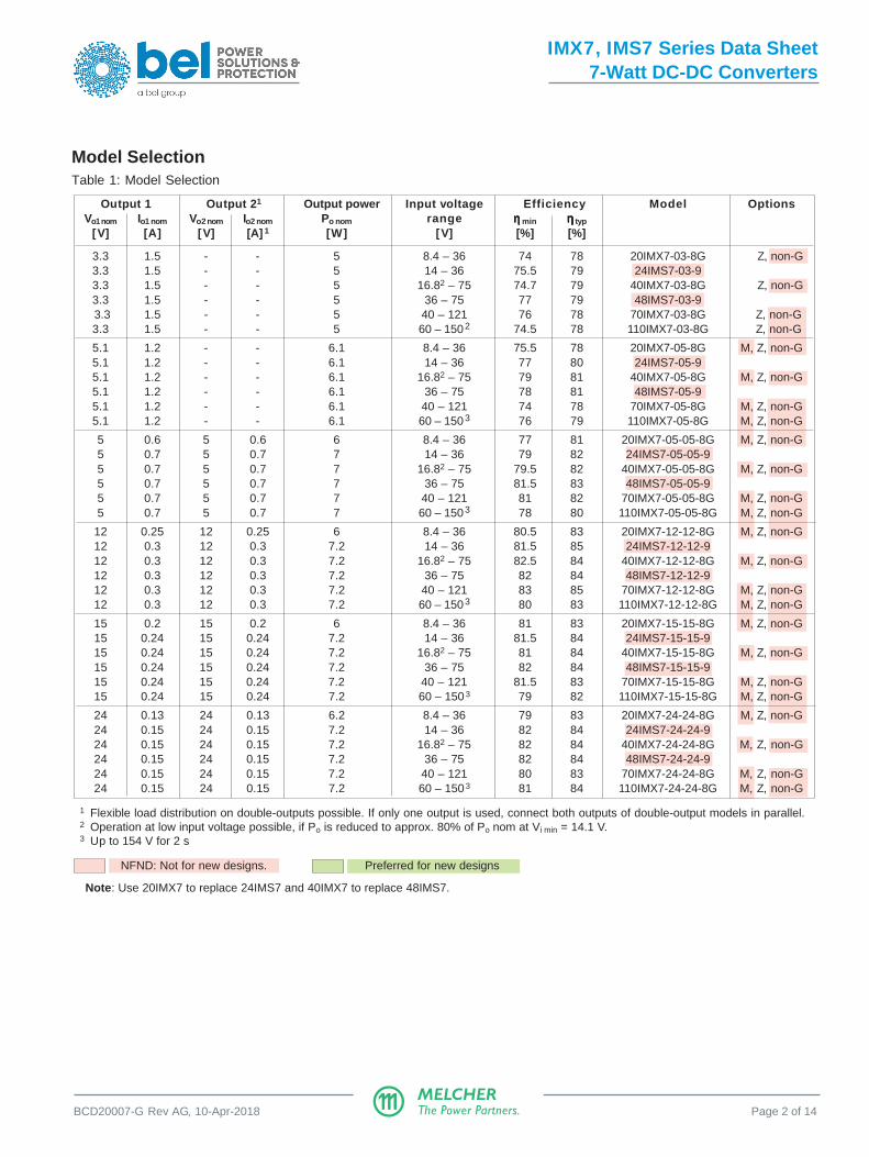
Model SelectionTable 1: Model Selection
Output 1 Output 21 Output power Input voltage Efficiency Model OptionsVo1 nom Io1 nom Vo2 nom Io2 nom Po nom range ηηηηη min ηηηηη typ
[V] [A] [V] [A] 1 [W] [V] [%] [%]
3.3 1.5 - - 5 8.4 – 36 74 78 20IMX7-03-8G Z, non-G3.3 1.5 - - 5 14 – 36 75.5 79 24IMS7-03-93.3 1.5 - - 5 16.82 – 75 74.7 79 40IMX7-03-8G Z, non-G3.3 1.5 - - 5 36 – 75 77 79 48IMS7-03-9 3.3 1.5 - - 5 40 – 121 76 78 70IMX7-03-8G Z, non-G3.3 1.5 - - 5 60 – 1502 74.5 78 110IMX7-03-8G Z, non-G
5.1 1.2 - - 6.1 8.4 – 36 75.5 78 20IMX7-05-8G M, Z, non-G5.1 1.2 - - 6.1 14 – 36 77 80 24IMS7-05-9 5.1 1.2 - - 6.1 16.82 – 75 79 81 40IMX7-05-8G M, Z, non-G5.1 1.2 - - 6.1 36 – 75 78 81 48IMS7-05-9 5.1 1.2 - - 6.1 40 – 121 74 78 70IMX7-05-8G M, Z, non-G5.1 1.2 - - 6.1 60 – 1503 76 79 110IMX7-05-8G M, Z, non-G
5 0.6 5 0.6 6 8.4 – 36 77 81 20IMX7-05-05-8G M, Z, non-G5 0.7 5 0.7 7 14 – 36 79 82 24IMS7-05-05-9 5 0.7 5 0.7 7 16.82 – 75 79.5 82 40IMX7-05-05-8G M, Z, non-G5 0.7 5 0.7 7 36 – 75 81.5 83 48IMS7-05-05-9 5 0.7 5 0.7 7 40 – 121 81 82 70IMX7-05-05-8G M, Z, non-G5 0.7 5 0.7 7 60 – 1503 78 80 110IMX7-05-05-8G M, Z, non-G
12 0.25 12 0.25 6 8.4 – 36 80.5 83 20IMX7-12-12-8G M, Z, non-G12 0.3 12 0.3 7.2 14 – 36 81.5 85 24IMS7-12-12-9 12 0.3 12 0.3 7.2 16.82 – 75 82.5 84 40IMX7-12-12-8G M, Z, non-G12 0.3 12 0.3 7.2 36 – 75 82 84 48IMS7-12-12-9 12 0.3 12 0.3 7.2 40 – 121 83 85 70IMX7-12-12-8G M, Z, non-G12 0.3 12 0.3 7.2 60 – 1503 80 83 110IMX7-12-12-8G M, Z, non-G
15 0.2 15 0.2 6 8.4 – 36 81 83 20IMX7-15-15-8G M, Z, non-G15 0.24 15 0.24 7.2 14 – 36 81.5 84 24IMS7-15-15-9 15 0.24 15 0.24 7.2 16.82 – 75 81 84 40IMX7-15-15-8G M, Z, non-G15 0.24 15 0.24 7.2 36 – 75 82 84 48IMS7-15-15-9 15 0.24 15 0.24 7.2 40 – 121 81.5 83 70IMX7-15-15-8G M, Z, non-G15 0.24 15 0.24 7.2 60 – 150 3 79 82 110IMX7-15-15-8G M, Z, non-G
24 0.13 24 0.13 6.2 8.4 – 36 79 83 20IMX7-24-24-8G M, Z, non-G24 0.15 24 0.15 7.2 14 – 36 82 84 24IMS7-24-24-9 24 0.15 24 0.15 7.2 16.82 – 75 82 84 40IMX7-24-24-8G M, Z, non-G24 0.15 24 0.15 7.2 36 – 75 82 84 48IMS7-24-24-9 24 0.15 24 0.15 7.2 40 – 121 80 83 70IMX7-24-24-8G M, Z, non-G24 0.15 24 0.15 7.2 60 – 150 3 81 84 110IMX7-24-24-8G M, Z, non-G
1 Flexible load distribution on double-outputs possible. If only one output is used, connect both outputs of double-output models in parallel.2 Operation at low input voltage possible, if Po is reduced to approx. 80% of Po nom at Vi min = 14.1 V.3 Up to 154 V for 2 s
NFND: Not for new designs. Preferred for new designs
Note: Use 20IMX7 to replace 24IMS7 and 40IMX7 to replace 48IMS7.
IMX7, IMS7 Series Data Sheet7-Watt DC-DC Converters
BCD20007-G Rev AG, 10-Apr-2018 Page 3 of 14MELCHERThe Power Partners.
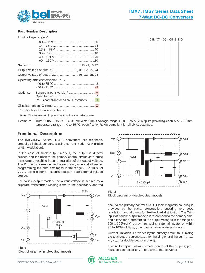
Functional DescriptionThe IMX7/IMS7 Series DC-DC converters are feedback-controlled flyback converters using current mode PWM (PulseWidth Modulation).
In the case of single-output models, the output is directlysensed and fed back to the primary control circuit via a pulsetransformer, resulting in tight regulation of the output voltage.The R input is referenced to the secondary side and allows forprogramming the output voltages in the range 75 to 105% ofVo nom, using either an external resistor or an external voltagesource.
For double-output models, the output voltage is sensed by aseparate transformer winding close to the secondary and fed
Fig. 2Block diagram of double-output models
Fig. 1Block diagram of single-output models
back to the primary control circuit. Close magnetic coupling isprovided by the planar construction, ensuring very goodregulation, and allowing for flexible load distribution. The Triminput of double-output models is referenced to the primary side,and allows for programming the output voltages in the range of100 to 105% of Vo nom by means of an external resistor, or within75 to 100% of Vo nom, using an external voltage source.
Current limitation is provided by the primary circuit, thus limitingthe total output current (Io nom for the single- and the sum Io1 nom
+ Io2 nom for double-output models).
The inhibit input i allows remote control of the outputs; pin imust be connected to Vi– to activate the converter.
Part Number Description
Input voltage range Vi
8.4 – 36 V .............................................. 2014 – 36 V ............................................... 2416.8 – 75 V ............................................ 4036 – 75 V ............................................... 4840 – 121 V ............................................. 7060 – 150 V ........................................... 110
Series .............................................................. IMX7, IMS7
Output voltage of output 1 ...................... 03, 05, 12, 15, 24
Output voltage of output 2 ............................ 05, 12, 15, 24
Operating ambient temperature TA
–40 to 85 °C ............................................... -8–40 to 71 °C ............................................... -9
Options: Surface mount version1 ........................................... MOpen frame1 ..................................................................... ZRoHS-compliant for all six substances ........ G
Obsolete option: C-pinout ............................................... C1 Option M and Z exclude each other.
Note: The sequence of options must follow the order above.
Example: 40IMX7-05-05-8ZG: DC-DC converter, input voltage range 16.8 – 75 V, 2 outputs providing each 5 V, 700 mA,temperature range –40 to 85 °C, open frame, RoHS compliant for all six substances.
40 IMX7 - 05 - 05 -8 Z G
PWM
2 × 2200 pF
1500 V
13
1
2
3
4
11
10
12
14
Vi+
i
Vi–
n.c.
Vo+
Vo–
R
n.c.
03025a
PWM
2 × 2200 pF 14
1
2
3
4
11
10
12
13
Vi+
Trim
i
Vi–
Vo1+
Vo1–
Vo2+
Vo2–
n.c.
03042b
IMX7, IMS7 Series Data Sheet7-Watt DC-DC Converters
BCD20007-G Rev AG, 10-Apr-2018 Page 4 of 14MELCHERThe Power Partners.
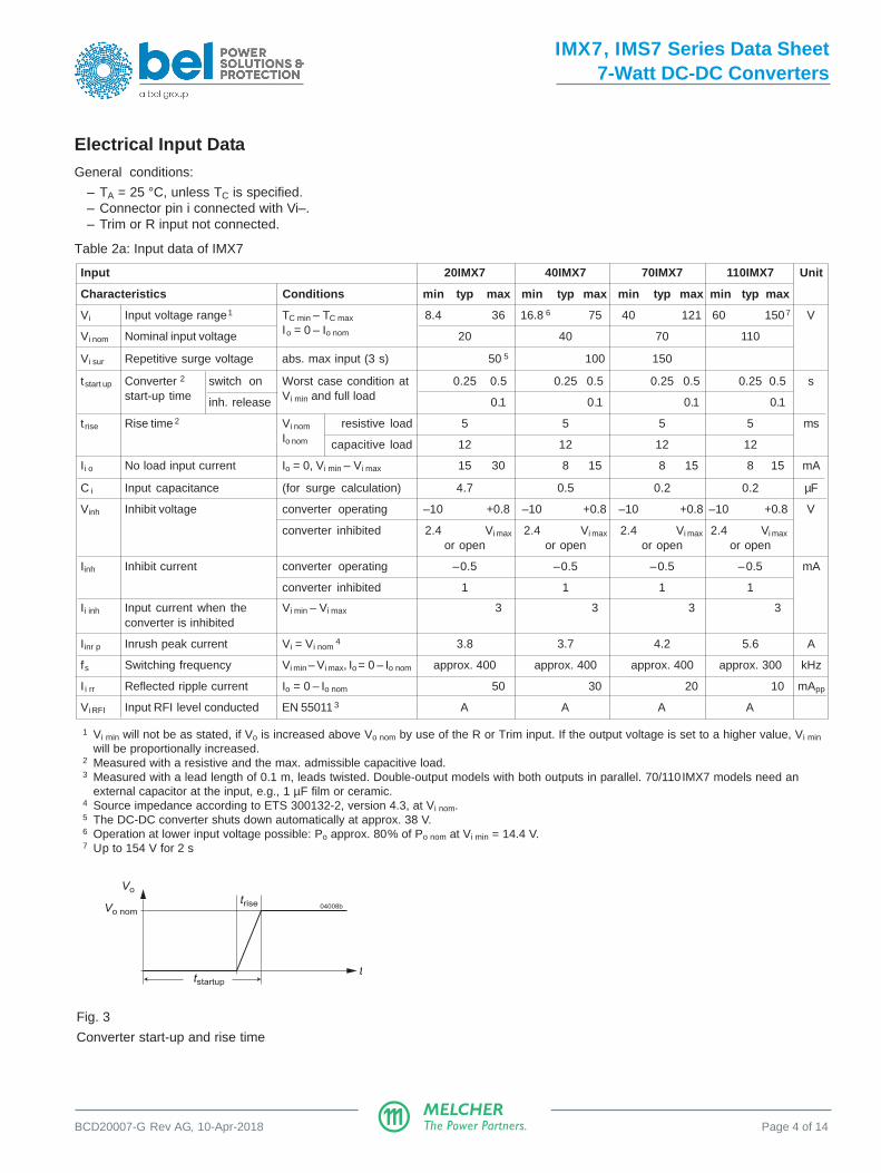
Electrical Input DataGeneral conditions:
– TA = 25 °C, unless TC is specified.– Connector pin i connected with Vi–.– Trim or R input not connected.
Table 2a: Input data of IMX7
Input 20IMX7 40IMX7 70IMX7 110IMX7 Unit
Characteristics Conditions min typ max min typ max min typ max min typ max
Vi Input voltage range1 TC min – TC max 8.4 36 16.8 6 75 40 121 60 150 7 V
Vi nom Nominal input voltage Io = 0 – Io nom 20 40 70 110
Vi sur Repetitive surge voltage abs. max input (3 s) 50 5 100 150
tstart up Converter 2 switch on Worst case condition at 0.25 0.5 0.25 0.5 0.25 0.5 0.25 0.5 sstart-up time inh. release Vi min and full load 0.1 0.1 0.1 0.1
t rise Rise time 2 Vi nom resistive load 5 5 5 5 msIo nom capacitive load 12 12 12 12
Ii o No load input current Io = 0, Vi min – Vi max 15 30 8 15 8 15 8 15 mA
C i Input capacitance (for surge calculation) 4.7 0.5 0.2 0.2 µF
Vinh Inhibit voltage converter operating –10 +0.8 –10 +0.8 –10 +0.8 –10 +0.8 V
converter inhibited 2.4 Vi max 2.4 Vi max 2.4 Vi max 2.4 Vi max
or open or open or open or open
Iinh Inhibit current converter operating –0.5 –0.5 –0.5 –0.5 mA
converter inhibited 1 1 1 1
Ii inh Input current when the Vi min – Vi max 3 3 3 3converter is inhibited
Iinr p Inrush peak current Vi = Vi nom 4 3.8 3.7 4.2 5.6 A
fs Switching frequency Vi min – Vi max, Io = 0 – Io nom approx. 400 approx. 400 approx. 400 approx. 300 kHz
I i rr Reflected ripple current Io = 0 – Io nom 50 30 20 10 mApp
Vi RFI Input RFI level conducted EN 55011 3 A A A A
1 Vi min will not be as stated, if Vo is increased above Vo nom by use of the R or Trim input. If the output voltage is set to a higher value, Vi min
will be proportionally increased.2 Measured with a resistive and the max. admissible capacitive load.3 Measured with a lead length of 0.1 m, leads twisted. Double-output models with both outputs in parallel. 70/110IMX7 models need an
external capacitor at the input, e.g., 1 µF film or ceramic.4 Source impedance according to ETS 300132-2, version 4.3, at Vi nom.5 The DC-DC converter shuts down automatically at approx. 38 V.6 Operation at lower input voltage possible: Po approx. 80% of Po nom at Vi min = 14.4 V.7 Up to 154 V for 2 s
Fig. 3
Converter start-up and rise time
Vo nom
Vo
tstartup
trise
t
04008b
IMX7, IMS7 Series Data Sheet7-Watt DC-DC Converters
BCD20007-G Rev AG, 10-Apr-2018 Page 5 of 14MELCHERThe Power Partners.
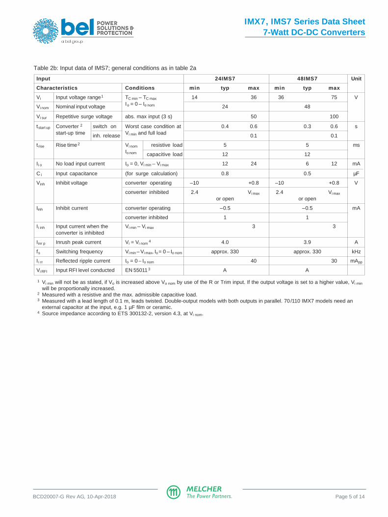
Table 2b: Input data of IMS7; general conditions as in table 2a
Input 24IMS7 48IMS7 Unit
Characteristics Conditions min typ max min typ max
Vi Input voltage range1 TC min – TC max 14 36 36 75 V
Vi nom Nominal input voltage Io = 0 – Io nom 24 48
Vi sur Repetitive surge voltage abs. max input (3 s) 50 100
tstart up Converter 2 switch on Worst case condition at 0.4 0.6 0.3 0.6 sstart-up time inh. release Vi min and full load 0.1 0.1
t rise Rise time 2 Vi nom resistive load 5 5 msIo nom capacitive load 12 12
Ii o No load input current Io = 0, Vi min – Vi max 12 24 6 12 mA
C i Input capacitance (for surge calculation) 0.8 0.5 µF
Vinh Inhibit voltage converter operating –10 +0.8 –10 +0.8 V
converter inhibited 2.4 Vi max 2.4 Vi max
or open or open
Iinh Inhibit current converter operating –0.5 –0.5 mA
converter inhibited 1 1
Ii inh Input current when the Vi min – Vi max 3 3converter is inhibited
Iinr p Inrush peak current Vi = Vi nom 4 4.0 3.9 A
fs Switching frequency Vi min – Vi max, Io = 0 – Io nom approx. 330 approx. 330 kHz
I i rr Reflected ripple current Io = 0 – Io nom 40 30 mApp
Vi RFI Input RFI level conducted EN 55011 3 A A
1 Vi min will not be as stated, if Vo is increased above Vo nom by use of the R or Trim input. If the output voltage is set to a higher value, Vi min
will be proportionally increased.2 Measured with a resistive and the max. admissible capacitive load.3 Measured with a lead length of 0.1 m, leads twisted. Double-output models with both outputs in parallel. 70 /110 IMX7 models need an
external capacitor at the input, e.g. 1 µF film or ceramic.4 Source impedance according to ETS 300132-2, version 4.3, at Vi nom.
IMX7, IMS7 Series Data Sheet7-Watt DC-DC Converters
BCD20007-G Rev AG, 10-Apr-2018 Page 6 of 14MELCHERThe Power Partners.
Input Transient Voltage Protection
In many applications transient voltages on the input of theconverter may occur and are possibly caused by short circuitsbetween Vi+ and Vi–, where the network inductance maycause high energy pulses.
In order to protect the converters, transient suppressors arefitted to the input; see table below:
Table 3: Built-in transient voltage suppressor
Model Breakdown Peak Power Peak PulseVoltage at 1 ms CurrentVBR nom P P IPP
20IMX7 1 overvoltage lockout at approx. 38 V
24IMS7 2 53 V 600 W 7.7 A
40IMX7 2 100 V 1500 W 11 A
48IMS7 2 100 V 600 W 4.1 A
70IMX7 2 144 V 600 W 2.9 A
110IMX7 2 167 V 600 W 2.5 A
1 The built-in overvoltage trigger disables the converter atapprox. 38 V protecting the input up to 50 V. For higher transientvoltages an external suppressor or voltage limiting circuit as,e.g., for IEC/EN 61000-4-5, level 2 compliance should beprovided.
2 If transients generating currents above the peak pulse currentare possible, an external limiting network such as the circuitrecommended for IEC/EN 61000-4-5, level 2 compliance, isnecessary.
To achieve IEC/EN 61000-4-5, level 2 compliance, anadditional inductor and capacitor should be providedexternally as shown in the figure below. The componentsshould have similar characteristics as listed in table 4.
Note: Suppressor diode D is only necessary for 20IMX7 models.
Input Fuse and Reverse Polarity Protection
The suppressor diode on the input also provides for reversepolarity protection by conducting current in the reversedirection, thus protecting the converter. An external fuse isrequired to limit this current. We recommend for:
– 20IMX7 and 24IMS7 a fast 2 A (F2A) fuse– 40IMX7 and 48IMS7 a fast 1 A (F1A) fuse– 70IMX7 a fast 0.63 A (F.63A) fuse– 110IMX7 a fast 0.63 A (F.63A) fuse.
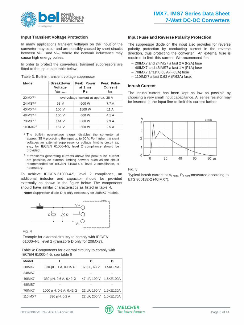
Inrush Current
The inrush current has been kept as low as possible bychoosing a very small input capacitance. A series resistor maybe inserted in the input line to limit this current further.
Fig. 5
Typical inrush current at Vi nom , Po nom measured according toETS 300132-2 (40IMX7).
0
1
2
3
A
0 20 40 60 80 µs
04030a
4
Table 4: Components for external circuitry to comply withIEC/EN 61000-4-5, see table 8
Model L C D
20IMX7 330 µH, 1 A, 0.115 Ω 68 µF, 63 V 1.5KE39A
24IMS7 – – –
40IMX7 330 µH, 0.6 A, 0.42 Ω 47 µF, 100 V 1.5KE100A
48IMS7 – – –
70IMX7 1000 µ H, 0.6 A, 0.42 Ω 22 µF, 160 V 1.5KE120A
110IMX7 330 µH, 0.2 A 22 µF, 200 V 1.5KE170A
Fig. 4
Example for external circuitry to comply with IEC/EN61000-4-5, level 2 (transzorb D only for 20IMX7).
Vi+
Vi–
07064
C
L
D+ i
IMX7, IMS7 Series Data Sheet7-Watt DC-DC Converters
BCD20007-G Rev AG, 10-Apr-2018 Page 7 of 14MELCHERThe Power Partners.
Electrical Output DataGeneral conditions:
– TA = 25 °C, unless TC is specified.– Pin i connected with Vi–; Trim or R input left open-circuit.
Table 5a: Output data for single-output models
Output Vo nom 3.3 V 5.1 V Unit
Characteristics Conditions min typ max min typ max
Vo Output voltage setting Vi nom 3.28 3.32 5.07 5.13 V
Io nom Output current (nom.) Vi min – Vi max 1.5 1.2 A
Io L Current limit 2 Vi nom 1.78 2.7 1.56 2.0
∆Vo Line and load regulation Vi min – Vi max ±1 ±1 %Io = (0.05 – 1) Io nom
vo Output voltage noise Vi min – Vi max5 70 70 mVpp
other models Io = Io nom 6 20 40 20 40
110IMX7 40 50 40 50
Vo clp Output overvoltage limit 7 Minimum load 1% 115 130 115 130 %
Co ext Admissible capacitive load 0 2500 0 2000 µF
Vo d Dynamic Voltage deviat. Vi nom ±250 ±250 mV
to dload Recovery time Io nom ↔ 1/2 Io nom 1 1 msregulation
αVo Temperature coefficient Vi min – Vi max ±0.02 ±0.02 %/K∆Vo/∆TC (TC min to TC max) Io = (0.05 – 1) Io nom
Table 5b: Output data for double-output models
Output Vo nom 2 × 5 V 2 × 12 V 2 ×15 V 2 × 24 V Unit
Characteristics Conditions min typ max min typ max min typ max min typ max
Vo1 Output voltage IMX7 Vi nom 4.96 5.04 11.90 12.10 14.88 15.12 23.81 24.19 VVo2 setting Io1 = Io2 = 0.5 Io nom 4.95 5.05 11.88 12.12 14.85 15.15 23.75 24.25
Vo1 IMS7 Vi nom 4.92 5.08 11.82 12.18 14.78 15.22 23.64 24.36Vo2 Io1 = Io2 = 0.5 Io nom 4.92 5.08 11.82 12.18 14.78 15.22 23.64 24.36
Io nom Output current 20IMX7 Vi min – Vi max 2 × 0.6 2 × 0.25 2 × 0.2 2 × 0.13 A(nom.)1
other models 2 × 0.7 2 × 0.3 2 × 0.24 2 × 0.15
Io L Current 20IMX7 Vi nom 1.8 2.1 0.7 0.9 0.5 0.7 0.35 0.45limit 2 3
other models 1.8 2.0 0.8 1.0 0.55 0.9 0.38 0.5
∆Vo1 Line regulation Vi min – Vi max, Io nom ±1 ±1 ±1 ±1 %
∆Vo l Load regulation 4 Vi nom , (0.1 – 1) Io nom ±3 ±3 ±3 ±3
vo1, 2 Output voltage noise Vi min – Vi ma5 80 120 150 240 mVpp
Io = Io nom 6 20 40 25 50 30 60 50 100
Vo clp Output overvoltage limit 7 Minimum load 1% 115 130 115 130 115 130 115 130 %
Co ext Admissible capacitive load3 0 2000 0 300 0 200 0 100 µF
Vo d Dynamic Voltage deviat. Vi nom ±150 ±330 ±350 ±600 mV
tdload Recovery time Io nom ↔ 1/2 Io nom 1 1 1 1 msregulation
αVo Temperature coefficient Vi min – Vi max ±0.02 ±0.02 ±0.02 ±0.02 %/Kof output voltage (0.05 – 1) Io nom
1 Each output is capable of delivering full output power Po nom according to table Model Selection.2 The current limit is primary side controlled. Io L is defined when Vo dropped to 85 to 94%.3 Measured with both outputs connected in parallel.4 Conditions for specified output. Other output loaded with constant current Io = 0.5 Io nom.5 BW = 20 MHz6 Measured with a probe according to EN 61204.7 The overvoltage protection is not tracking with the R control.

IMX7, IMS7 Series Data Sheet7-Watt DC-DC Converters
BCD20007-G Rev AG, 10-Apr-2018 Page 8 of 14MELCHERThe Power Partners.
Thermal Considerations
If the converter, mounted on a PCB, is located in free, quasi-stationary air (convection cooling) at the maximum ambienttemperature TA max (see table Temperature specifications) andis operated at nominal input voltage and output power, thecase temperature TC measured at the measuring point of casetemperature (see Mechanical Data) will approach TC max afterthe warm-up phase. However, the relationship between TA andTC depends heavily on the conditions of operation andintegration into a system, such as input voltage, output current,airflow, temperature of surrounding components and surfaces,and the properties of the printed circuit board. TA max istherefore only an indicative value, and under practicaloperating conditions, TA may be higher or lower.
Caution: The case temperature TC measured at the measuringpoint of case temperature (see Mechanical Data) may under nocircumstances exceed the specified maximum. The installer mustensure that under all operating conditions TC remains within thelimits stated in the table Temperature specifications.
Fig. 8a
Vo versus Io (typ.) of single-output models with Vo = 5.1 V
Fig. 8b
Vo versus Io (typ.) of double-output models (2 ×12 V) with bothoutputs in parallel
Short-Circuit Behavior
The current limitation shuts down the converter, when a shortcircuit is applied to the output. It acts self-protecting, andautomatically recovers after removal of the overload condition.
Output Overvoltage Protection
The outputs are protected against overvoltage by Zenerdiodes. In the event of an overvoltage, the converter will shutdown and attempt to restart automatically. The main purposeof this feature is to protect against possible overvoltage, whichcould occur due to a failure in the feedback control circuit. Theconverters are not designed to withstand external overvoltagesapplied to the outputs.
Series or Parallel Connection
The outputs of single- or double-output models can beconnected in series without any precautions, taking intoconsideration that the output voltage should remain below 60 Vfor SELV operation.
Both outputs of double-output models can be connected inparallel without any precautions. Several converters (single- ordouble-output models) with equal output voltage can be put inparallel and will share their output current quite equally.However, this may cause start-up problems and is onlyrecommended in applications, where one converter is able todeliver the full load current, e.g., in true redundant systems.
Fig. 7
Overload switch-off (hiccup mode).
5.5
5.0
4.5
4.0
3.5
3.00 0.4 0.8 1.2 1.6 Io [A]
Vo [V]05087a
1.0
0.8
0.6
0.4
0
0.2
20 40 60 80 100 °C
Po/Po max
JM017
TA
0.5 m/s = 100 LFM
natural cooling
70
100
Vo [%]
t
05041c
0.3 s
overload condition
switch-off
0
Fig. 6
Maximum allowed output power versus ambient temperature
7
8
9
10
11
12
13
Vo [V]
0.2 0.4 0.6 0.8 Io total [A]0
05086b
IMX7, IMS7 Series Data Sheet7-Watt DC-DC Converters
BCD20007-G Rev AG, 10-Apr-2018 Page 9 of 14MELCHERThe Power Partners.
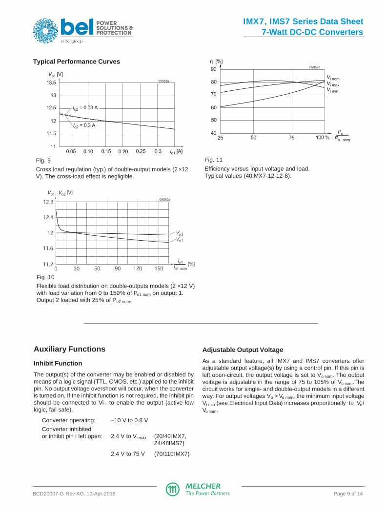
Fig. 10
Flexible load distribution on double-outputs models (2 ×12 V)with load variation from 0 to 150% of Po1 nom on output 1.Output 2 loaded with 25% of Po2 nom.
Vo1, Vo2 [V]
Io1 Io1 nom
05059a12.8
12.4
12
11.6
11.20 30 60 90 120 150
[%]
Vo2Vo1
Typical Performance Curves
Fig. 9
Cross load regulation (typ.) of double-output models (2 ×12V). The cross-load effect is negligible.
11
11.5
12
12.5
13
13.5
Vo1 [V]
0.10 0.15 0.20 0.25 0.3 Io1 [A]0.05
05088a
Io2 = 0.3 A
Io2 = 0.03 A
Fig. 11
Efficiency versus input voltage and load.Typical values (40IMX7-12-12-8).
40
50
60
70
80
9005052a
25 50 75 100 %Po Po nom
Vi nom
Vi max
Vi min
η [%]
Auxiliary Functions
Inhibit Function
The output(s) of the converter may be enabled or disabled bymeans of a logic signal (TTL, CMOS, etc.) applied to the inhibitpin. No output voltage overshoot will occur, when the converteris turned on. If the inhibit function is not required, the inhibit pinshould be connected to Vi– to enable the output (active lowlogic, fail safe).
Converter operating: –10 V to 0.8 V
Converter inhibitedor inhibit pin i left open: 2.4 V to Vi max (20/40IMX7,
24/48IMS7)
2.4 V to 75 V (70/110IMX7)
Adjustable Output Voltage
As a standard feature, all IMX7 and IMS7 converters offeradjustable output voltage(s) by using a control pin. If this pin isleft open-circuit, the output voltage is set to Vo nom. The outputvoltage is adjustable in the range of 75 to 105% of Vo nom.Thecircuit works for single- and double-output models in a differentway. For output voltages Vo > Vo nom, the minimum input voltageVi min (see Electrical Input Data) increases proportionally to Vo/Vo nom.
IMX7, IMS7 Series Data Sheet7-Watt DC-DC Converters
BCD20007-G Rev AG, 10-Apr-2018 Page 10 of 14MELCHERThe Power Partners.
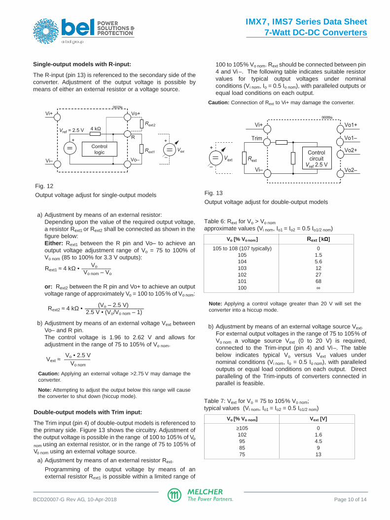
Fig. 12
Output voltage adjust for single-output models
Single-output models with R-input:
The R-input (pin 13) is referenced to the secondary side of theconverter. Adjustment of the output voltage is possible bymeans of either an external resistor or a voltage source.
Trim
Vo1+
Vo2–
+
Vext
–
Vi+
Vi–
Rext
Vo1–
Vo2+
06089a
Controlcircuit
Vref 2.5 V
Fig. 13
Output voltage adjust for double-output models
Double-output models with Trim input:
The Trim input (pin 4) of double-output models is referenced tothe primary side. Figure 13 shows the circuitry. Adjustment ofthe output voltage is possible in the range of 100 to 105% of Vo
nom using an external resistor, or in the range of 75 to 105% ofVo nom using an external voltage source.
a) Adjustment by means of an external resistor Rext.
Programming of the output voltage by means of anexternal resistor Rext1 is possible within a limited range of
b) Adjustment by means of an external voltage source Vext.For external output voltages in the range of 75 to 105% ofVo nom a voltage source Vext (0 to 20 V) is required,connected to the Trim-input (pin 4) and Vi–. The tablebelow indicates typical Vo versus Vext values undernominal conditions (Vi nom, Io = 0.5 Io nom), with paralleledoutputs or equal load conditions on each output. Directparalleling of the Trim-inputs of converters connected inparallel is feasible.
100 to 105% Vo nom. Rext should be connected between pin4 and Vi–. The following table indicates suitable resistorvalues for typical output voltages under nominalconditions (Vi nom, Io = 0.5 Io nom), with paralleled outputs orequal load conditions on each output.
Caution: Connection of Rext to Vi+ may damage the converter.
R
Vo+
Vo–
+
Vext
–
4 kΩVref = 2.5 V
Control
logic Rext1
Rext2
06029e
Vi–
Vi+
+
a) Adjustment by means of an external resistor:Depending upon the value of the required output voltage,a resistor Rext1 or Rext2 shall be connected as shown in thefigure below:Either: Rext1 between the R pin and Vo– to achieve anoutput voltage adjustment range of Vo = 75 to 100% ofVo nom (85 to 100% for 3.3 V outputs):
Vo Rext1 ≈ 4 kΩ • ––––––––– Vo nom – Vo
or: Rext2 between the R pin and Vo+ to achieve an outputvoltage range of approximately Vo = 100 to 105% of Vo nom:
(Vo – 2.5 V) Rext2 ≈ 4 kΩ • –––––––––––––––––– 2.5 V • (Vo/Vo nom – 1)
b) Adjustment by means of an external voltage Vext betweenVo– and R pin.The control voltage is 1.96 to 2.62 V and allows foradjustment in the range of 75 to 105% of Vo nom.
Vo • 2.5 V Vext ≈ ––––––––
Vo nom
Caution: Applying an external voltage >2.75 V may damage theconverter.
Note: Attempting to adjust the output below this range will causethe converter to shut down (hiccup mode).
Table 6: Rext for Vo > Vo nom
approximate values (Vi nom, Io1 = Io2 = 0.5 Io1/2 nom)
Vo [% Vo nom] Rext [kΩΩΩΩΩ]
105 to 108 (107 typically) 0105 1.5104 5.6103 12102 27101 68100 ∞
Note: Applying a control voltage greater than 20 V will set theconverter into a hiccup mode.
Table 7: Vext for Vo = 75 to 105% Vo nom;typical values (Vi nom, Io1 = Io2 = 0.5 Io1/2 nom)
Vo [% Vo nom] Vext [V]
≥105 0102 1.695 4.585 975 13
IMX7, IMS7 Series Data Sheet7-Watt DC-DC Converters
BCD20007-G Rev AG, 10-Apr-2018 Page 11 of 14MELCHERThe Power Partners.
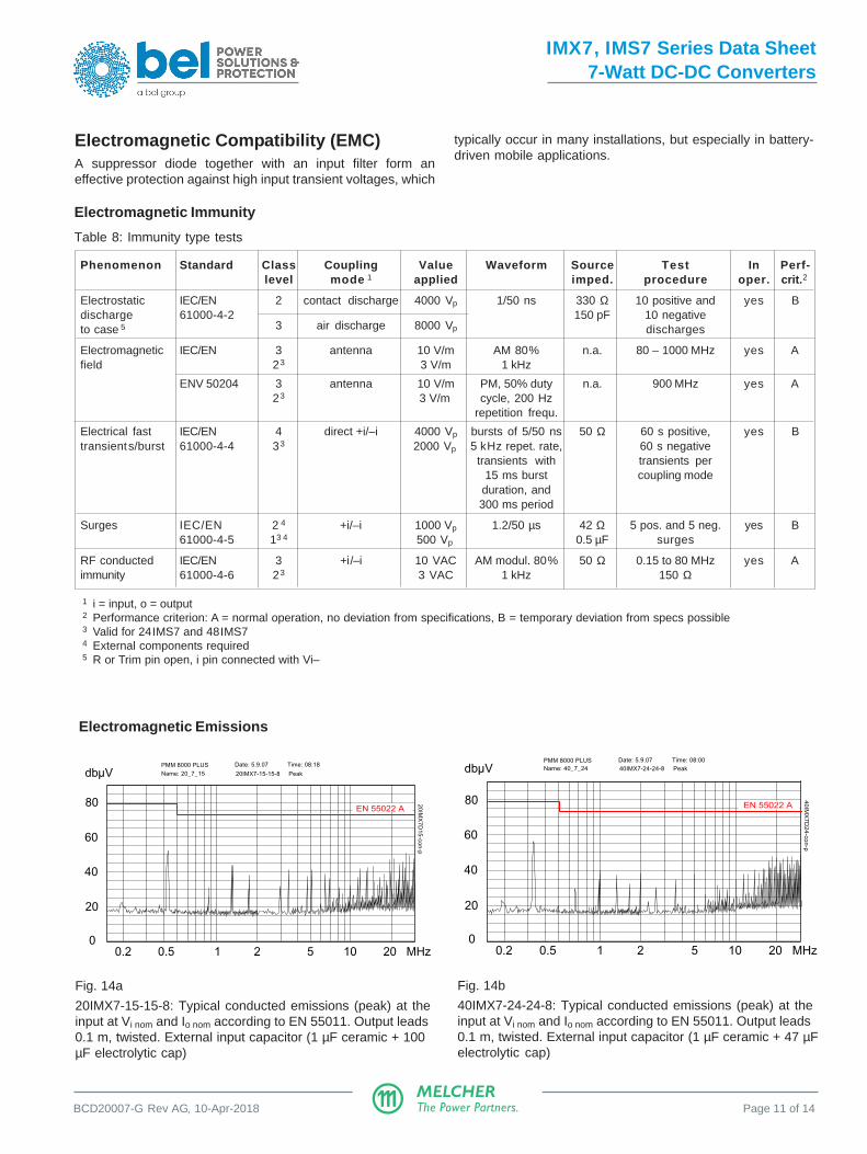
Electromagnetic Emissions
typically occur in many installations, but especially in battery-driven mobile applications.
Electromagnetic Compatibility (EMC)A suppressor diode together with an input filter form aneffective protection against high input transient voltages, which
Fig. 14a
20IMX7-15-15-8: Typical conducted emissions (peak) at theinput at Vi nom and Io nom according to EN 55011. Output leads0.1 m, twisted. External input capacitor (1 µF ceramic + 100µF electrolytic cap)
Electromagnetic Immunity
Table 8: Immunity type tests
Phenomenon Standard Class Coupling Value Waveform Source Test In Perf-level mode 1 applied imped. procedure oper. crit. 2
Electrostatic IEC/EN 2 contact discharge 4000 Vp 1/50 ns 330 Ω 10 positive and yes Bdischarge 61000-4-2
3 air discharge 8000 Vp
150 pF 10 negativeto case 5 discharges
Electromagnetic IEC/EN 3 antenna 10 V/m AM 80% n.a. 80 – 1000 MHz yes Afield 2 3 3 V/m 1 kHz
ENV 50204 3 antenna 10 V/m PM, 50% duty n.a. 900 MHz yes A2 3 3 V/m cycle, 200 Hz
repetition frequ.
Electrical fast IEC/EN 4 direct +i/–i 4000 Vp bursts of 5/50 ns 50 Ω 60 s positive, yes Btransients/burst 61000-4-4 3 3 2000 Vp
5 kHz repet. rate, 60 s negativetransients with transients per
15 ms burst coupling modeduration, and300 ms period
Surges IEC/EN 2 4 +i/–i 1000 Vp 1.2/50 µs 42 Ω 5 pos. and 5 neg. yes B61000-4-5 13 4 500 Vp
0.5 µF surges
RF conducted IEC/EN 3 +i/–i 10 VAC AM modul. 80% 50 Ω 0.15 to 80 MHz yes Aimmunity 61000-4-6 2 3 3 VAC 1 kHz 150 Ω
1 i = input, o = output2 Performance criterion: A = normal operation, no deviation from specifications, B = temporary deviation from specs possible3 Valid for 24IMS7 and 48IMS74 External components required5 R or Trim pin open, i pin connected with Vi–
PMM 8000 PLUS Date: 5.9.07 Time: 08:00
40IMX
7D24-con-p
dbµV
80
60
20
40
0 0.2 0.5 1 2 5 10 20 MHz
EN 55022 A
40IMX7-24-24-8 PeakName: 40_7_24
20IMX7-15-15-8 Peak
PMM 8000 PLUSName: 20_7_15
Date: 5.9.07 Time: 08:18
20IMX
7D15-con-p
dbµV
80
60
20
40
0 0.2 0.5 1 2 5 10 20 MHz
EN 55022 A
Fig. 14b
40IMX7-24-24-8: Typical conducted emissions (peak) at theinput at Vi nom and Io nom according to EN 55011. Output leads0.1 m, twisted. External input capacitor (1 µF ceramic + 47 µFelectrolytic cap)

IMX7, IMS7 Series Data Sheet7-Watt DC-DC Converters
BCD20007-G Rev AG, 10-Apr-2018 Page 12 of 14MELCHERThe Power Partners.
PMM 8000 PLUS Date: 5.9.07 Time: 08:00
110IMX
7-05-con-p
dbµV
80
60
20
40
0
110IMX7-05-8 PeakName: 110_7_05
0.2 0.5 1 2 5 10 20 MHz
EN 55022 A
Immunity to Environmental ConditionsTable 9: Mechanical and climatic stress
Test Method Standard Test conditions Status
Cab Damp heat IEC/EN 60068-2-78 Temperature: 40 ±2 °C Convertersteady state MIL-STD-810D section 507.2 Relative humidity: 93 +2/-3 % not
Duration: 56 days operating
Ea Shock IEC/EN 60068-2-27 Acceleration amplitude: 100 gn = 981 m/s2 Converter(half-sinusoidal) MIL-STD-810D section 516.3 Bump duration: 6 ms operating
Number of bumps: 18 (3 each direction)
Fc Vibration IEC/EN 60068-2-6 Acceleration amplitude: 0.35 mm (10 to 60 Hz) Converter(sinusoidal) 5 gn = 49 m/s2 (60 to 2000 Hz) operating
Frequency (1 Oct/min): 10 to 2000 HzTest duration: 7.5 h (2.5 h each axis)
Fh Vibration, IEC/EN 60068-2-64 Acceleration spectral density: 0.05 gn2/Hz Converter
broad-band Frequency band: 10 to 500 Hz operatingrandom Acceleration magnitude: 4.9 gn rms
(digital control) Test duration: 3 h (1 h each axis)
Kb Salt mist, cyclic IEC/EN 60068-2-52 Concentration: 5% (30 °C) Converter(sodium chloride Duration: 2 h per cycle notNaCl solution) Storage: 40 °C, 93% rel. humidity operating
Storage duration: 22 h per cycleNumber of cycles: 3
Fig. 15
48IMS7-15-15-8: Typical conducted emissions (peak) at theinput at Vi nom and Io nom according to EN 55011. Output leads0.1 m, twisted. External input capacitor (1 µF ceramic + 47 µFelectrolytic cap).
PMM 8000 PLUS Date: 5.9.07 Time: 09:10
dbµV
80
60
20
40
0
48IMS7-15-15-8 PeakName: 48_7_15
0.2 0.5 1 2 5 10 20 MHz
EN 55022 A
Fig. 14c
110IMX7-05-8: Typical conducted emissions (peak) at theinput at Vi nom and Io nom according to EN 55011. Output leads0.1 m, twisted. External input capacitor (0.15 µF ceramic +4.7 µF electrolytic cap).
Table 10: Temperature specifications, valid for air pressure of 800 to 1200 hPa (800 to 1200 mbar)
Temperature -9 -8 Unit
Characteristics Conditions min max min max
TA Ambient temperature Operational 1 –40 71 –40 85 °C
TC Case temperature –40 95 –40 105
TS Storage temperature Non operational –55 100 –55 85
1 See Thermal Considerations
Temperatures
IMX7, IMS7 Series Data Sheet7-Watt DC-DC Converters
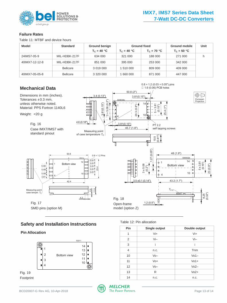
BCD20007-G Rev AG, 10-Apr-2018 Page 13 of 14MELCHERThe Power Partners.
50.8 (2")
3.81(0.15")
3.8
1(0
.15")
3.81(0.15")
5 ×
3.8
1
(0.1
5")
20.3
(0.8
")
3 ×
5.0
8 (
0.2
")
PT 2.2
self tapping screws
1
410
14
0.8 × 1.2 (0.03 × 0.05") pins
∅ 1.6 (0.06) PCB holes
10.5
(0.4
1")
3.4 (0.13")
45.7 (1.8")
25.4
(1")
4.6 (0.18")
S09030b
Measuring point
of case temperature TC
Mechanical DataDimensions in mm (inches).Tolerances ±0.3 mm,unless otherwise noted.Material: PPS Fortron 1140L6
Weight: <20 g
Fig. 16
Case IMX7/IMS7 withstandard pinout
EuropeanProjection
Failure Rates
Safety and Installation Instructions
Pin Allocation
Fig. 19
Footprint
Bottom view
1
410
14
10011
2
3 11
12
13
Table 12: Pin allocation
Pin Single output Double output
1 Vi+ Vi+
2 Vi– Vi–
3 i i
4 n.c. Trim
10 Vo– Vo1–
11 Vo+ Vo1+
12 Vo– Vo2–
13 R Vo2+
14 n.c. n.c.
Fig. 18
Open-framemodel (option Z)
Fig. 17
SMD pins (option M)
Table 11: MTBF and device hours
Model Standard Ground benign Ground fixed Ground mobile Unit
TC = 40 °C TC = 40 °C TC = 70 °C TC = 50 °C
24IMS7-05-9 MIL-HDBK-217F 634 000 321 000 188 000 271 000 h
40IMX7-12-12-8 MIL-HDBK-217F 851 000 395 000 253 000 342 000
Bellcore 3 019 000 1 510 000 809 000 409 000
40IMX7-05-05-8 Bellcore 3 320 000 1 660 000 871 000 447 000
43.2 (1.7")
S90002b
48 (1.9")1.2
7 (
0.0
5")
23 (
0.9
")
5 x
3.8
1
(0.1
5")
8.2
5
(0.3
2")
3 x
5.0
8
(0.2
")
1
410
14
3.5 ±0.1 (0.14")
1.2 (0.5")
Bottom view
TC Z
Core
50.8
3.81
3.81
3.81
3.81
3.81
5.08
5.08
5.08
3.81
1
410
14
0.8 × 1.2 Pins
25
.4
4.2
0.8
11
.0
42.4
09031a
Measuring point
case temper. TC
Bottom view
IMX7, IMS7 Series Data Sheet7-Watt DC-DC Converters
BCD20007-G Rev AG, 10-Apr-2018 Page 14 of 14MELCHERThe Power Partners.
Standards and Approvals
The converters are safety-approved to the latest edition of IEC/EN 60950-1 and UL/CSA 60950-1.
The converters have been evaluated for: • Building-in • Basic insulation input to output, based on their maximum
input voltage• Pollution degree 2 environment• Connecting the input to a secondary circuit, which is
subject to a maximum transient rating of
- 1500 V for 20IMX7, 24IMS7, 40IMX7, 48IMS7- 2000 V for 70IMX7- 2500 V for 110IMX7.
The converters are subject to manufacturing surveillance inaccordance with the above mentioned standards and ISO9001.
Railway Applications
To comply with railway standards, all components are coatedwith a protective lacquer (except option Z).
Protection Degree and Cleaning Liquids
The protection degree of the converters is IP 30, except open-frame models (option Z).
In order to avoid possible damage, any penetration of cleaningfluids should be prevented, since the power supplies are nothermetically sealed.
However, open-frame models (option Z) leave the factoryunlacquered; they may be lacquered by the customer, forinstance together with the mother board. Cleaning agents arenot permitted – except washing at room temperature withisopropyl alcohol. If necessary, the mother board must becleaned, before fitting the open-frame converter.
Note: Cleaning liquids may damage the adhesive joints of theferrite cores.
Isolation
The electric strength test is performed in the factory as a routinetest in accordance with EN 50514 and IEC/EN 60950, andshould not be repeated in the field. The Company will not honorany warranty claims resulting from electric strength field tests.
Installation Instruction
Installation of the converters must strictly follow the nationalsafety regulations in compliance with the enclosure, mounting,creepage, clearance, casualty, markings, and segregationrequirements of the end-use application.
Connection to the system shall be made via a printed circuitboard; see Mechanical Data.
The converters should be connected to a secondary circuit.
Do not open the converter.
Ensure that a converter failure does not result in a hazardousconditions.
To prevent excessive current flowing through the input lines incase of a short-circuit, an external fuse specified in sectionInput Fuse and Reverse Polarity Protection should be installedin the non-earthed input supply line.
Description of Options
Option M: SMD pins
This option allows surface mounting of the converters.
Option Z: Open Frame
For applications, where the protection by a housing is not
necessary or in the case that the motherboard should belacquered after fitting the converter; see Cleaning Liquids.
Option G: RoHS-6
Converters with a type designation ending by G are RoHS-compliant for all six substances.
NUCLEAR AND MEDICAL APPLICATIONS - These products are not designed or intended for use as critical components in life support systems,equipment used in hazardous environments, or nuclear control systems.
TECHNICAL REVISIONS - The appearance of products, including safety agency certifications pictured on labels, may change depending on thedate manufactured. Specifications are subject to change without notice.
Copyright © 2018, Bel Power Solutions Inc. All rights reserved. belfuse.com/power-solutions
Table 12: Electric strength test voltages
Characteristic Input to output o/o 3 Unit20/40IMX 20/40IMX2 110IMX24/48IMS 70IMX
Factory test >1 s 1.2 1.51 2.0 0.1 kVAC
Equivalent DC volt. (1.5) (2.1) (2.5) 0.15 kVDC
Coupling 1.2 1.2 1.2 – nFcapacitance
Insulation resist. >100 >100 >100 – MΩat 500 VDC
1 1.5 kVAC according to IEC 60950, sect. 6.2, Telecom equipment;type test with 1.5 kVAC / 60 s (IEE 802.3).
2 20/40IMX7 produced 2014 or later.3 The test voltage between outputs is not applied as routine test.