i.mx50 applications plastic package processors for
TRANSCRIPT

Freescale SemiconductorData Sheet: Technical Data
Document Number: IMX50CECRev. 7, 10/2013
MCIMX50
Package InformationPlastic Package
Case 416 MAPBGA 13 x 13 mm, 0.5 mm pitchCase 416 PoPBGA 13 x 13 mm, 0.5 mm pitchCase 400 MAPBGA 17 x 17 mm, 0.8 mm pitch
Ordering Information
See Table 1 on page 7 for ordering information.
© 2011–2013 Freescale Semiconductor, Inc. All rights reserved.
Freescale reserves the right to change the detail specifications as may be requiredto permit improvements in the design of its products.
1 IntroductionThe i.MX50 applications processors are multimedia-focused products offering high-performance processing optimized for lowest power consumption. The i.MX50 processors are Freescale Energy Efficiency Solutions products.
The i.MX50 is optimized for portable multimedia applications and features Freescale’s advanced implementation of the ARM Cortex-A8® core, which operates at speeds as high as 1 GHz. The i.MX50 provides a powerful display architecture, including a 2D Graphics Processing Unit (GPU) and Pixel Processing Pipeline (ePXP). Additionally, the i.MX50 includes a complete integration of the electrophoretic display function. The i.MX50 supports DDR2, LPDDR2, and LPDDR1 DRAM at clock rate up to 266 MHz to enable a range of performance and power trade-offs.
The flexibility of the i.MX50 architecture allows it to be used in a variety of applications. As the heart of the
i.MX50 Applications Processors for Consumer Products
1. Introduction . . . . . . . . . . . . . . . . . . . . . . . . . . . . . . . . . . . 11.1. Product Overview . . . . . . . . . . . . . . . . . . . . . . . . . . 21.2. Features . . . . . . . . . . . . . . . . . . . . . . . . . . . . . . . . . 31.3. Ordering Information . . . . . . . . . . . . . . . . . . . . . . . 71.4. Part Number Feature Comparison . . . . . . . . . . . . . 81.5. Package Feature Comparison . . . . . . . . . . . . . . . . 9
2. Architectural Overview . . . . . . . . . . . . . . . . . . . . . . . . . . 102.1. Block Diagram . . . . . . . . . . . . . . . . . . . . . . . . . . . 10
3. Modules List . . . . . . . . . . . . . . . . . . . . . . . . . . . . . . . . . . 113.1. Special Signal Considerations . . . . . . . . . . . . . . . 17
4. Electrical Characteristics . . . . . . . . . . . . . . . . . . . . . . . . 204.1. Chip-Level Conditions . . . . . . . . . . . . . . . . . . . . . 214.2. Supply Power-Up/Power-Down Requirements and
Restrictions . . . . . . . . . . . . . . . . . . . . . . . . . . . . . 294.3. I/O DC Parameters . . . . . . . . . . . . . . . . . . . . . . . . 314.4. Output Buffer Impedance Characteristics . . . . . . 374.5. I/O AC Parameters . . . . . . . . . . . . . . . . . . . . . . . . 414.6. System Modules Timing . . . . . . . . . . . . . . . . . . . . 484.7. External Interface Module (EIM) . . . . . . . . . . . . . . 604.8. DRAM Timing Parameters . . . . . . . . . . . . . . . . . . 684.9. External Peripheral Interfaces . . . . . . . . . . . . . . . 73
5. Package Information and Contact Assignments . . . . . 1015.1. 13 x 13 mm, 0.5 mm Pitch, 416 Pin MAPBGA Package
Information . . . . . . . . . . . . . . . . . . . . . . . . . . . . . 1015.2. 13 x 13 mm, 0.5 mm Pitch, 416 Pin PoPBGA Package
Information . . . . . . . . . . . . . . . . . . . . . . . . . . . . . 1095.3. 17 x 17 mm, 0.8 mm Pitch, 400 Pin MAPBGA Package
Information . . . . . . . . . . . . . . . . . . . . . . . . . . . . . 1165.4. Signal Assignments . . . . . . . . . . . . . . . . . . . . . . 124
6. Revision History . . . . . . . . . . . . . . . . . . . . . . . . . . . . . . 134

i.MX50 Applications Processors for Consumer Products, Rev. 7
Introduction
Freescale Semiconductor2
application chipset, the i.MX50 provides a rich set of interfaces for connecting peripherals, such as WLAN, Bluetooth™, GPS, and displays.
1.1 Product OverviewThe i.MX50 is designed to enable high-tier portable applications by satisfying the performance requirements of advanced operating systems and applications.
1.1.1 Dynamic Performance Scaling
Freescale’s dynamic voltage and frequency scaling (DVFS) allows the device to run at much lower voltage and frequency with ample processing capacity for tasks, such as audio decode, resulting in significant power reduction.
1.1.2 Multimedia Processing Powerhouse
The multimedia performance of the i.MX50 processor ARM Cortex-A8 core is boosted by a multi-level cache system, a NEON™ coprocessor with SIMD media processing architecture and 32-bit single-precision floating point support, and two vector floating point coprocessors. The system is further enhanced by a programmable smart DMA (SDMA) controller.
1.1.3 Powerful Display System
The i.MX50 includes support for both standard LCD displays as well as electrophoretic displays (e-paper). The display subsystem consists of the following modules:
• Electrophoretic Display Controller (EPDC) (i.MX508 only)
The EPDC is a feature-rich, low power, and high-performance direct-drive active matrix EPD controller. It is specifically designed to drive E-INKTM EPD panels, supporting a wide variety of TFT architectures. The goal of the EPDC is to provide an efficient SoC integration of this functionality for e-paper applications, allowing a significant bill of materials cost savings over an external solution while reaching much higher levels of performance and lower power. The EPDC module is defined in the context of an optimized hardware/software partitioning and works in conjunction with the ePXP (see Section 1.1.4, “Graphics Accelerators”).
• Enhanced LCD Controller Interface (eLCDIF)
The eLCDIF is a high-performance LCD controller interface that supports a rich set of modes and allows interoperability with a wide variety of LCD panels, including DOTCK/RGB and smart panels. The module also supports synchronous operation with the ePXP to allow the processed frames to be passed from the ePXP to the eLCDIF through an on-chip SRAM buffer. The eLCDIF can support up to 32-bit interfaces.
1.1.4 Graphics Accelerators
Integrated graphics accelerators offload processing from the ARM processor, enabling high performance graphic applications at minimum power.

Introduction
i.MX50 Applications Processors for Consumer Products, Rev. 7
Freescale Semiconductor 3
• Pixel Processing Pipeline (ePXP)
The ePXP is a high-performance pixel processor capable of 1 pixel/clock performance for combined operations, such as color-space conversion, alpha blending, gamma mapping, and rotation. The ePXP is enhanced with features specifically for grayscale applications working in conjunction with the electrophoretic display controller to form a full grayscale display solution. In addition, the ePXP supports traditional pixel/frame processing paths for still-image and video processing applications, allowing it to interface with the integrated LCD controller (eLCDIF).
• Graphics acceleration
The i.MX50 provides a 2D graphics accelerator with performance up to 200 Mpix/s.
1.1.5 Multilevel Memory System
The multilevel memory system of the i.MX50 is based on the L1 instruction and data caches, L2 cache, and internal and external memory. The i.MX50 supports many types of external memory devices, including DDR2, LPDDR2, LPDDR1, NOR Flash, PSRAM, Cellular RAM, NAND Flash (MLC and SLC) and OneNAND™, and managed NAND including eMMC up to rev. 4.4.
1.1.6 Smart Speed™ Technology
The i.MX50 device has power management throughout the SOC that enables the rich suite of multimedia features and peripherals to consume minimum power in both active and various low power modes. Smart Speed technology enables the designer to deliver a feature-rich product that requires levels of power that are far less than industry expectations.
1.1.7 Interface Flexibility
The i.MX50 supports connection to a variety of interfaces, including an LCD controller for displays, two high-speed USB on-the-go-capable PHYs, multiple expansion card ports (high-speed MMC/SDIO host and others), 10/100 Ethernet controller, and a variety of other popular interfaces (for example, UART, I2C, and I2S serial audio).
1.1.8 Advanced Security
The i.MX50 delivers hardware-enabled security features, such as High-Assurance Boot 4 (HAB4) for signed/authenticated firmware images, basic DRM support with random private keys and AES encryption/decryption, and storage and programmability of on-chip fuses.
1.2 FeaturesThe i.MX50 applications processor is based on the ARM Cortex-A8 platform and has the following features:
• MMU, L1 instruction cache, and L1 data cache
• Unified L2 cache
• 800 MHz or 1 GHz target frequency of the core (including NEON, VFPv3, and L1 cache)

i.MX50 Applications Processors for Consumer Products, Rev. 7
Introduction
Freescale Semiconductor4
• NEON coprocessor (SIMD Media Processing Architecture) and Vector Floating Point (VFP-Lite) coprocessor supporting VFPv3
The memory system consists of the following components:
• Level 1 cache:
— Instruction (32 Kbyte)
— Data (32 Kbyte)
• Level 2 cache:
— Unified instruction and data (256 Kbyte)
• Level 2 (internal) memory:
— Boot ROM, including HAB (96 Kbyte)
— Internal multimedia/shared, fast access RAM (128 Kbyte)
• External memory interfaces:
— 16/32-bit DDR2-533, LPDDR2-533, or LPDDR1-400 up to a total of 2 GByte
— 8-bit NAND SLC/MLC Flash with up to 100 MHz synchronous clock rate and up to 32-bit hardware ECC for 1 Kbyte block size
— 16/32-bit NOR Flash with a dedicated 16-bit muxed-mode interface. I/O muxing logic selects EIMv2 port as primary muxing at system boot.
— 16-bit PSRAM, Cellular RAM
— Managed NAND, including eMMC up to rev 4.4
The i.MX50 introduces a next generation system bus fabric architecture that aggregates various sub-system buses and masters for access to system peripherals and memories. The various bus-systems and components are as follows:
• 64-bit AXI Fabric (266 MHz)—This bus-fabric is the SoC’s central bus aggregation point.
— Provides access to all slave targets in the SoC:
– ROM (ROMCP)
– On-chip RAM (OCRAM)
– External DRAM (DRAM MC)
– External static RAM (EIM)
– Interrupt controller (TZIC)
– Decode into the AHB MAX crossbar second level AHB fabric.
— Provides arbitration to the following masters in the system:
– ARM CPU complex
– Pixel processing pipeline (ePXP)
– Electrophoretic display controller (EPDC)
– eLCDIF LCD display controller
– DCP Crypto engine
– BCH ECC engine
– MAX AHB crossbar

Introduction
i.MX50 Applications Processors for Consumer Products, Rev. 7
Freescale Semiconductor 5
– GPU 2D
– SDMA
– USBOH1 (USB OTG and host controller complex)
– FEC Ethernet controller
• MAX AHB crossbar (133 MHz)—This connects the various AHB bus sub-segments in the system and provides decode into the following slaves:
— IP-Bus 1 (66 MHz)—This bus segment contains peripherals accessible by the ARM core and without DMA capability
— IP-Bus 2 (66 MHz)—This bus segment contains peripherals accessible by the ARM core and without DMA capability
— APBH DMA bridge (133 MHz)—The APBH DMA bridge is a master to the MAX for its memory-side DMA operations. The APBH bus is an AMBA APB slave bus providing peripheral access to many of the high-speed IP blocks on the i.MX50.
• IP-Bus 3 (66 MHz)—This third peripheral bus segment contains peripherals accessible by the ARM core and SDMA and as such houses peripherals with DMA capability. The IP-Bus 3 can be accessed by the ARM CPU through IP-Bus 1 and SPBA.
• Quality of service controller (QoSC)—This provides both soft and dynamic arbitration/priority control. The QoSC works in conjunction with the critical display modules such as the eLCDIF and EPDC to provide dynamic priority control, based on real-time metrics.
The i.MX50 makes use of dedicated hardware accelerators to achieve state-of-the-art multimedia performance. The use of hardware accelerators provides both high performance and low power consumption, while freeing up the CPU core for other tasks.
The i.MX50 incorporates the following hardware accelerators:
• GPU2Dv1—2D Graphics accelerator, OpenVG 1.1, 200 Mpix/s performance
• ePXP—enhanced PiXel Processing Pipeline off loading key pixel processing operations required to support both LCD and EPD display applications
The i.MX50 includes the following interfaces to external devices:
NOTENot all the interfaces are available simultaneously depending on I/O multiplexer configuration.
• Displays:
— EPDC (i.MX508 Only)—Supporting direct-driver TFT backplanes beyond 2048 × 1536 at 106 Hz refresh (or 4096 × 4096 at 20 Hz)
— eLCDIF—Supporting beyond SXGA + (1400 × 1050) at 60 Hz resolutions with up to a 32-bit display interface
— On the i.MX508, both displays can be active simultaneously. If both displays are active, the eLCDIF only provides a 16-bit interface due to pin muxing.
• Expansion cards:
— Four SD/MMC card

i.MX50 Applications Processors for Consumer Products, Rev. 7
Introduction
Freescale Semiconductor6
• USB:
— One High Speed (HS) USB 2.0 OTG-capable port with integrated HS USB PHY
— One High Speed (HS) USB 2.0 host port with integrated HS USB PHY
• Miscellaneous interfaces:
— One-wire (OWIRE) port
— Two I2S/SSI/AC97 ports, supporting up to 1.4 Mbps each connected to the Audio Multiplexer (AUDMUX) providing four external ports
— Five UART RS232 ports, up to 4.0 Mbps each
— Two eCSPI (Enhanced CSPI) ports, up to 66 Mbps each plus CSPI port, up to 16.6 Mbps
— Three I2C ports, supporting 400 kbps
— Fast Ethernet controller IEEE 802.3, 10/100 Mbps
— Key pad port (KPP)
— Two pulse width modulators (PWM)
— GPIO with interrupt capabilities
— Secure JTAG controller (SJC)
The system supports efficient and smart power control and clocking:
• Supporting DVFS techniques for low power modes, including auto slow architecture
• Power gating-SRPG (state retention power gating) for ARM core and NEON
• Support for various levels of system power modes
• Flexible clock gating control scheme
• On-chip temperature monitor
• On-chip 32 kHz and 24 MHz oscillators
• A total of four PLLs with the fourth PLL providing up to eight independently controllable outputs, improving the ease of clocking control, especially for display and connectivity modules
Security functions are enabled and accelerated by the following hardware:
• Secure JTAG controller (SJC)—Protecting JTAG from debug port attacks by regulating or blocking the access to the system debug features
• Secure real-time clock (SRTC)—Tamper resistant RTC with dedicated power domain and mechanism to detect voltage and clock glitches
• Advanced high assurance boot (A-HAB)—HAB with the next embedded enhancements: SHA-256, 2048-bit RSA key, version control mechanism, warm boot, CSU, and TZ initialization

Introduction
i.MX50 Applications Processors for Consumer Products, Rev. 7
Freescale Semiconductor 7
1.3 Ordering InformationTable 1 provides the ordering information.
Table 1. Ordering Information
Part NumberMaximum ARM CLK Frequency
Mask Set
Features
Temperature Range (°C)
Package1
1 Case MAPBGA is RoHS compliant, lead-free MSL (Moisture Sensitivity Level) 3.
Tambient Tjunction
MCIMX508CVK1B 1 GHz N78A Full Specification 0 to 70 0 to 90 13 x 13 mm, 0.5 mm pitch BGACase: 416 MAPBGA
MCIMX508CVM1B 1 GHz N78A Full Specification 0 to 70 0 to 90 17 x 17 mm, 0.8 mm pitch BGACase: 400 MAPBGA
MCIMX508CVK8B 800 MHz N78A Full Specification 0 to 70 0 to 90 13 x 13 mm, 0.5 mm pitch BGA Case: 416 MAPBGA
MCIMX508CZK8B 800 MHz N78A Full Specification 0 to 70 0 to 90 13 x 13 mm, 0.5 mm pitch BGA Case: 416 PoPBGA
MCIMX508CVM8B 800 MHz N78A Full Specification 0 to 70 0 to 90 17 x 17 mm, 0.8 mm pitch BGA Case: 400 MAPBGA
MCIMX507CVM1B 1 GHz N78A No GPU 0 to 70 0 to 90 17 x 17 mm, 0.8 mm pitch BGACase: 400 MAPBGA
MCIMX507CVK1B 1 GHz N78A No GPU 0 to 70 0 to 90 13 x 13 mm, 0.5 mm pitch BGACase: 416 MAPBGA
MCIMX507CVM8B 800 MHz N78A No GPU 0 to 70 0 to 90 17 x 17 mm, 0.8 mm pitch BGA Case: 400 MAPBGA
MCIMX507CVK8B 800 MHz N78A No GPU 0 to 70 0 to 90 13 x 13 mm, 0.5 mm pitch BGA Case: 416 MAPBGA
MCIMX503CVK8B 800 MHz N78A No EPD controller 0 to 70 0 to 90 13 x 13 mm, 0.5 mm pitch BGA Case: 416 MAPBGA
MCIMX503CVM8B 800 MHz N78A No EPD controller 0 to 70 0 to 90 17 x 17 mm, 0.8 mm pitch BGA Case: 400 MAPBGA
MCIMX503EVM8B 800 MHz N78A No EPD controller,Extended Temperature
-20 to 70 -20 to 90 17 x 17 mm, 0.8 mm pitch BGA Case: 400 MAPBGA
MCIMX502CVK8B 800 MHz N78A No GPU, no EPD controller 0 to 70 0 to 90 13 x 13 mm, 0.5 mm pitch BGA Case: 416 MAPBGA
MCIMX502CVM8B 800 MHz N78A No GPU, no EPD controller 0 to 70 0 to 90 17 x 17 mm, 0.8 mm pitch BGA Case: 400 MAPBGA
MCIMX502EVM8B 800 MHz N78A No GPU, no EPD controller, Extended Temperature
-20 to 70 -20 to 90 17 x 17 mm, 0.8 mm pitch BGA Case: 400 MAPBGA

i.MX50 Applications Processors for Consumer Products, Rev. 7
Introduction
Freescale Semiconductor8
1.4 Part Number Feature ComparisonTable 2 provides an overview of the feature differences between the i.MX50 part numbers.
Table 2. Part Number Feature Comparison
Part Number Disabled Features Comments
MCIMX508 None
MCIMX507 GPU
MCIMX503 EPDC The i.MX503 has the same ball map and IOMUX as the i.MX508. The EPDC pins still exist on the i.MX503, but because the EPDC block is disabled, those pins cannot be used for EPDC functionality (ALT0) and must be configured in the IOMUX with another ALT-mode setting.
MCIMX502 GPU, EPDC The i.MX502 has the same ball map and IOMUX as the i.MX508. The EPDC pins still exist on the i.MX502, but because the EPDC block is disabled, those pins cannot be used for EPDC functionality (ALT0) and must beconfigured in the IOMUX with another ALT-mode setting.

Introduction
i.MX50 Applications Processors for Consumer Products, Rev. 7
Freescale Semiconductor 9
1.5 Package Feature ComparisonTable 3 provides an overview of the feature and pin differences between the i.MX50 packages.
Table 3. Package Feature Comparison
Package DimensionsI/O Pin Differences
Versus 416 MAPBGANotes on Package Differences
416 MAPBGA 13 x 13 mm, 0.5 mm pitch
— • USB_OTG_VDDA25 and USB_H1_VDDA25 are shorted together on the 416 MAPBGA package substrate.
• USB_OTG_VDDA33 and USB_H1_VDDA33 are shorted together on the 416 MAPBGA package substrate.
416 PoPBGA 13 x 13 mm, 0.5 mm pitch
Deleted Pins:DRAM_A10DRAM_A11DRAM_A12DRAM_A13DRAM_A14DRAM_CASDRAM_OPENDRAM_OPENFBDRAM_RASDRAM_SDBA0DRAM_SDBA1DRAM_SDBA2DRAM_SDCLK_1DRAM_SDCLK_1_BDRAM_SDODT0DRAM_SDODT1DRAM_SDWEDRAM_OPENDRAM_OPENFB
Added Pins:POP_EMMC_RSTPOP_LPDDR2_ZQ0POP_LPDDR2_ZQ1POP_LPDDR2_1.8VPOP_NAND_VCC
• The i.MX50 PoPBGA package supports 168-FBGA LPDDR2 DRAM memory only. It is not possible to support LPDDR1 or DDR2 on the i.MX50 PoPBGA.
• i.MX50 PoPBGA was designed to accommodate a combined LPDDR2 / eMMC PoP memory. The PoP eMMC device uses the SD3_DATA[7:0], SD3_CLK, and SD3_CMD pins. Because the PoP eMMC I/O and memory supplies are tied together on the substrate, 1.8 V eMMC I/O operation is not supported for the PoP eMMC device. POP_NAND_VCC and NVCC_NANDF must use a 3 V supply.
• The NVCC_EMI_DRAM power pins supply 1.2 V power to the i.MX50 DRAM controller as well as the PoP LPDDR2 DRAM.
• Additional PoP package pin descriptions may be found in the Special Signals Considerations section (Table 5).
• On the PoPBGA package, the DRAM Address, Data, and clock pins are routed to the bottom balls for Freescale test purposes only. It is recommended that these bottom DRAM pins are left unconnected on the customer PCB.
• USB_OTG_VDDA25 and USB_H1_VDDA25 are shorted together on the 416 PoPBGA package substrate.
• USB_OTG_VDDA33 and USB_H1_VDDA33 are shorted together on the 416 PoPBGA package substrate.
400 MAPBGA 17 x 17 mm, 0.8 mm pitch
Deleted Pins:DRAM_SDCLK_1DRAM_SDCLK_1_BDRAM_A14DRAM_SDODT1UART2_CTSUART2_RTS
• USB_OTG_VDDA25 and USB_H1_VDDA25 are independent and NOT shorted together on the 400 MAPBGA package substrate.
• USB_OTG_VDDA33 and USB_H1_VDDA33 are independent and NOT shorted together on the 400 MAPBGA package substrate.

i.MX50 Applications Processors for Consumer Products, Rev. 7
Architectural Overview
Freescale Semiconductor10
2 Architectural OverviewThe following sections provide an architectural overview of the i.MX50 processor system.
2.1 Block DiagramFigure 1 shows the functional modules in the i.MX50 processor system.
Figure 1. i.MX50 System Block Diagram

Modules List
i.MX50 Applications Processors for Consumer Products, Rev. 7
Freescale Semiconductor 11
NOTEThe numbers in brackets indicate the number of module instances. For example, PWM (2) indicates two separate PWM peripherals.
3 Modules ListThe i.MX50 processor contains a variety of digital and analog modules that are described in Table 4 in alphabetical order.
Table 4. i.MX50 Digital and Analog Modules
Block Mnemonic
Block Name Subsystem Brief Description
ARM Cortex-A8
ARM Cortex-A8 Platform
ARM The ARM Cortex-A8 Core Platform consists of the ARM Cortex-A8 processor and its essential sub-blocks. It contains the 32 Kbyte L1 instruction cache, 32 Kbyte L1 data cache, Level 2 cache controller and a 256 Kbyte L2 cache. The platform also contains an event monitor and debug modules. It also has a NEON coprocessor with SIMD media processing architecture, register file with 32 × 64-bit general-purpose registers, an Integer execute pipeline (ALU, Shift, MAC), dual, single-precision floating point execute pipeline (FADD, FMUL), load/store and permute pipeline, and a non-pipelined vector floating point (VFP Lite) coprocessor supporting VFPv3.
EPDC Electrophoretic Display Controller
Display Peripherals
The EPDC is a feature-rich, low power, and high-performance direct-drive active matrix EPD controller. It is specifically designed to drive E-INKTM EPD panels supporting a wide variety of TFT backplanes.
ePXP enhanced PiXel Processing Pipeline
Display Peripherals
A high-performance pixel processor capable of 1 pixel/clock performance for combined operations such as color-space conversion, alpha blending, gamma-mapping, and rotation. The ePXP is enhanced with features specifically for grayscale applications. In addition, the ePXP supports traditional pixel/frame processing paths for still-image and video processing applications allowing it to interface with the integrated LCD controller (eLCDIF).
eLCDIF enhanced LCD Interface
Display Peripherals
The eLCDIF is a high-performance LCD controller interface supporting a rich set of modes allowing inter operability with a wide variety of LCD panels, including DOTCK/RGB and smart panels. The module also supports a synchronous operation with the ePXP to allow the processed frames to be passed from the ePXP to the eLCDIF through an on-chip SRAM buffer. The eLCDIF can support up to 32-bit interfaces.
AUDMUX Digital Audio Mux
Slave Connectivity Peripherals
The AUDMUX is a programmable interconnect for voice, audio, and synchronous data routing between host serial interfaces (for example, SSI1 and SSI2) and peripheral serial interfaces (audio and voice codecs). The AUDMUX has six ports (two internal and four external) with identical functionality and programming models. A desired connectivity is achieved by configuring two or more AUDMUX ports.
CAMP-1 Clock Amplifier Clocks, Resets, and Power Control
Clock Amplifier

i.MX50 Applications Processors for Consumer Products, Rev. 7
Modules List
Freescale Semiconductor12
CCMGPCSRC
Clock Control ModuleGlobal Power ControllerSystem Reset Controller
Clocks, Resets, and Power Control
These modules are responsible for clock and reset distribution in the system, and also for system power management.The system includes four PLLs.
CSPIeCSPI-1eCSPI-2
Configurable SPI, Enhanced CSPI
Slave Connectivity Peripherals
Full-duplex enhanced synchronous serial interface, with data rate up to 66.5 Mbit/s (for eCSPI, master mode). It is configurable to support Master/Slave modes, four chip selects to support multiple peripherals.
DAPTPIUCTI
Debug System System Control Peripherals
The Debug System provides real-time trace debug capability of both instructions and data. It supports a trace protocol that is an integral part of the ARM Real Time Debug solution (RealView).Real-time tracing is controlled by specifying a set of triggering and filtering resources, which include address and data comparators, three cross-system triggers (CTI), counters, and sequencers.Debug access port (DAP)—The DAP provides real-time access for the debugger without halting the core to System memory and peripheral registers. All debug configuration registers and Debugger access to JTAG scan chains.
DRAM MC DRAM Memory Controller
External Memory Interface
The DRAM MC consists of a DRAM memory controller and PHY, supporting LPDDR2, DDR2, and LPDDR1 memories with clock frequencies up to 266 MHz with 32-bit interface. It is tightly linked with the system bus fabric and employs advanced arbitration mechanism to maximize DRAM bandwidth efficiency.
EIM Static Memory Controller
External Memory Interface
The EIM is an external static memory and generic host interface. It supports up to a 32-bit interface (through pin-muxing) or a dedicated 16-bit muxed interface. It can be used to interface to PSRAMs (sync and async), NOR-flash or any external memory mapped peripheral.
BCH32/GPMI2 Raw NAND System with ECC
RawNAND and SSP Peripherals
The i.MX50 contains a fully hardware accelerated raw NAND flash solution supporting SLC and MLC devices. The system consists of the GPMI2 module, which is driven by the APBH DMA engine to perform the NAND flash interface function (supporting up to ONFI2.1). Coupled with the GPMI2 is the BCH32 hardware error-correction engine which is an AXI bus-master and supports up to 32-bits of correction over block sizes up to 1 Kbyte (that is, supports up to 2 Kbyte code-size).
System Fabric and QoS
System Fabric and QoS
System Peripherals
In order to aggregate the multitude of masters and memory mapped devices, the i.MX50 contains a next-generation AMBA3 AXI bus fabric. In addition, the i.MX50 contains a Quality of Service Controller IP (QoSC) which allows both soft priority control and dynamic priority elevation. Software priority control works for all masters but dynamic hardware control only works for EPDC and eLCDIF.
EPIT Enhanced Periodic Interrupt Timer
Timer Peripherals
Each EPIT is a 32-bit set and forget timer that starts counting after the EPIT is enabled by software. It is capable of providing precise interrupts at regular intervals with minimal processor intervention. It has a 12-bit prescaler for division of input clock frequency to get the required time setting for the interrupts to occur, and counter values can be programmed on the fly.
Table 4. i.MX50 Digital and Analog Modules (continued)
Block Mnemonic
Block Name Subsystem Brief Description

Modules List
i.MX50 Applications Processors for Consumer Products, Rev. 7
Freescale Semiconductor 13
eSDHCv3-3 (eMMC 4.4)
Ultra-High-Speed Multi-Media Card/Secure Digital card host controller, ver. 3
Master Connectivity Peripherals
Ultra High-Speed eSDHC, enhanced to support eMMC 4.4 standard specification, for 832 Mbps.IP is backward compatible to eSDHCv2 IP. See complete features listing in eSDHCv2 entry below.Port 3 is specifically enhanced to support eMMC 4.4 specification, for double data rate (832 Mbps, 8-bit port).
eSDHCv2-1eSDHCv2-2
eSDHCv2-4
Enhanced Multi-Media Card/Secure Digital Host Controller, ver. 2
In Enhanced Multi-Media Card/Secure Digital Host Controller the Ports 1, 2, and 4 are compatible with the MMC System Specification version 4.3, full supportThe generic features of the eSDHCv2 module, when serving as SD/MMC host, include the following: • Can be configured either as SD/MMC controller • Supports eSD and eMMC standard, for SD/MMC embedded type cards • Conforms to SD Host Controller Standard Specification version 2.0, full
support • Compatible with the SD Memory Card Specification version 1.1 • Compatible with the SDIO Card Specification version 1.2 • Designed to work with SD Memory, miniSD Memory, SDIO, miniSDIO, SD
Combo, MMC and MMC RS cards • Configurable to work in one of the following modes:
—SD/SDIO 1-bit, 4-bit—MMC 1-bit, 4-bit, 8-bit
• Full/High speed mode • Host clock frequency variable between 32 kHz to 52 MHz • Up to 200 Mbps data transfer for SD/SDIO cards using four parallel data
lines • Up to 416 Mbps data transfer for MMC cards using eight parallel data lines
FEC Fast Ethernet Controller
Master Connectivity Peripherals
The Ethernet Media Access Controller (MAC) is designed to support both 10 Mbps and 100 Mbps Ethernet/IEEE Std 802.3™ networks. An external transceiver interface and transceiver function are required to complete the interface to the media.
GPIO-1GPIO-2GPIO-3GPIO-4GPIO-5GPIO-6
General Purpose I/O Modules
Slave Connectivity Peripherals
These modules are used for general purpose input/output to external ICs. Each GPIO module supports up to 32 bits of I/O.
GPT General Purpose Timer
Timer Peripherals
Each GPT is a 32-bit free-running or set and forget mode timer with a programmable prescaler and compare and capture register. A timer counter value can be captured using an external event, and can be configured to trigger a capture event on either the leading or trailing edges of an input pulse. When the timer is configured to operate in “set and forget” mode, it is capable of providing precise interrupts at regular intervals with minimal processor intervention. The counter has output compare logic to provide the status and interrupt at comparison. This timer can be configured to run either on an external clock or on an internal clock.
Table 4. i.MX50 Digital and Analog Modules (continued)
Block Mnemonic
Block Name Subsystem Brief Description

i.MX50 Applications Processors for Consumer Products, Rev. 7
Modules List
Freescale Semiconductor14
GPU2Dv1 Graphics Processing Unit-2D, ver. 1
Display Peripherals
The GPU2Dv1 provides hardware acceleration for 2D graphic algorithms with sufficient processor power to run desk-top quality interactive graphics applications on displays up to HD1080 resolution.
I2C-1I2C-2I2C-3
I2C Interface Connectivity Peripherals
I2C provides serial interface for controlling peripheral devices. Data rates of up to 400 kbps are supported.
OCOTP Controller
On-chip OTP controller
Security Peripherals
The on-chip one-time -programmable (OCOTP) ROM serves the functions of hardware and software capability bits, Freescale operations and unique-ID, the customer-programmable cryptography key, and storage of various ROM and general purpose configuration bits.
IOMUXC IOMUX Control Slave Connectivity Peripherals
This module enables flexible I/O multiplexing. Each I/O pad has default as well as several alternate functions. The alternate functions are software configurable.
KPP Keypad Port Slave Connectivity Peripherals
The KPP supports an 8 × 8 external keypad matrix. The KPP features are as follows: • Open drain design • Glitch suppression circuit design • Multiple keys detection • Standby key press detection
OWIRE One-Wire Interface
Slave Connectivity Peripherals
One-Wire support provided for interfacing with an on-board EEPROM, and smart battery interfaces, for example, Dallas DS2502.
PWM-1PWM-2
Pulse Width Modulation
Slave Connectivity Peripherals
The pulse-width modulator (PWM) has a 16-bit counter and is optimized to generate sound from stored sample audio images. It can also generate tones. The PWM uses 16-bit resolution and a 4 x 16 data FIFO to generate sound.
RAM 128 Kbytes
Internal RAM Internal Memory
The On-Chip Memory controller (OCRAM) module, is an interface between the system’s AXI bus, to the internal (on-chip) SRAM memory module. It is used for controlling the 128 Kbyte multimedia RAM, through a 64-bit AXI bus.
ROM96 Kbytes
Boot ROM Internal Memory
Supports secure and regular Boot Modes.The ROM Controller supports ROM Patching.
Table 4. i.MX50 Digital and Analog Modules (continued)
Block Mnemonic
Block Name Subsystem Brief Description

Modules List
i.MX50 Applications Processors for Consumer Products, Rev. 7
Freescale Semiconductor 15
SDMA Smart Direct Memory Access
Master Connectivity Peripherals
The SDMA is multi-channel flexible DMA engine. It helps in maximizing system performance by offloading various cores in dynamic data routing.The SDMA features list is as follows: • Powered by a 16-bit instruction-set micro-RISC engine • Multi-channel DMA supports up to 32 time-division multiplexed DMA
channels • 48 events with total flexibility to trigger any combination of channels • Memory accesses including linear, FIFO, and 2D addressing • Shared peripherals between ARM Cortex-A8 and SDMA • Very fast context-switching with two-level priority-based preemptive
multi-tasking • DMA units with auto-flush and prefetch capability • Flexible address management for DMA transfers (increment, decrement,
and no address changes on source and destination address) • DMA ports can handle uni-directional and bi-directional flows (copy mode) • Up to 8-word buffer for configurable burst transfers for EMI • Support of byte-swapping and CRC calculations • A library of scripts and API is available
SJC Secure JTAG Controller
System Control Peripherals
The Secure JTAG Controller provides a mechanism for regulating JTAG access, preventing unauthorized JTAG usage while allowing JTAG access for manufacturing tests and software debugging. The i.MX50 JTAG port provides debug access to several hardware blocks including the ARM processor and the system bus, therefore, it must be accessible for initial laboratory bring-up, manufacturing tests and troubleshooting, and for software debugging by authorized entities. However, if the JTAG port is left unsecured it provides a method for executing unauthorized program code, getting control over secure applications, and running code in privileged modes. The Secure JTAG controller provides three different security modes that can be selected through an e-fuse configuration to prevent unauthorized JTAG access.
SPBA Shared Peripheral Bus Arbiter
System Control Peripherals
SPBA (Shared Peripheral Bus Arbiter) is a two-to-one IP bus interface (IP bus) arbiter.
SRTC Secure Real Time Clock
Security Peripherals
The SRTC incorporates a special System State Retention Register (SSRR) that stores system parameters during system shutdown modes. This register and all SRTC counters are powered by dedicated supply rail NVCC_SRTC. The NVCC_SRTC can be energized separately even if all other supply rails are shut down. This register is helpful for storing warm boot parameters. The SSRR also stores the system security state. In case of a security violation, the SSRR marks the event (security violation indication).
Table 4. i.MX50 Digital and Analog Modules (continued)
Block Mnemonic
Block Name Subsystem Brief Description

i.MX50 Applications Processors for Consumer Products, Rev. 7
Modules List
Freescale Semiconductor16
SSI-1SSI-2
I2S/SSI/AC97 Interface
Slave Connectivity Peripherals
The SSI is a full-duplex synchronous interface used on the i.MX50 processor to provide connectivity with off-chip audio peripherals. The SSI interfaces connect internally to the AUDMUX for mapping to external ports. The SSI supports a wide variety of protocols (SSI normal, SSI network, I2S, and AC-97), bit depths (up to 24 bits per word), and clock/frame sync options.Each SSI has two pairs of 8 x 24 FIFOs and hardware support for an external DMA controller in order to minimize its impact on system performance. The second pair of FIFOs provides hardware interleaving of a second audio stream, which reduces CPU overhead in use cases where two time slots are being used simultaneously.
Temperature Monitor
Temp Sensor Analog The temperature sensor is an internal module to the i.MX50 that monitors the die temperature.
UART-1UART-2UART-3UART-4UART-5
UART Interface, ver. 2
Slave Connectivity Peripherals
Each of the UARTv2 modules supports the following serial data transmit/receive protocols and configurations: • 7 or 8-bit data words, 1 or 2 stop bits, programmable parity (even, odd, or
none) • Programmable bit-rates up to 4 Mbps. This is a higher max baud rate
relative to the 1.875 Mbps, which is specified by the TIA/EIA-232-F standard.
• 32-byte FIFO on Tx and 32 half-word FIFO on Rx supporting auto-baud • IrDA 1.0 support (up to SIR speed of 115200 bps)
USB-OH-1 USB 2.0 High-Speed OTG-capable and Host ports
Master Connectivity Peripherals
USB-OH-1 supports USB2.0 HS/FS/LS, and contains: • One high-speed OTG-capable module with integrated HS USB PHY • One high-speed Host module with integrated HS USB PHY
WDOG-1 Watch Dog Timer Peripherals
The Watchdog (WDOG) timer module protects against system failures by providing a method of escaping from unexpected events or programming errors. The WDOG Timer supports two comparison points during each counting period. Each of the comparison points is configurable to invoke an interrupt to the ARM core, and a second point invokes an external event on the WDOG line.
XTALOSC Crystal Oscillator I/F
Clocking The XTALOSC module combined with an external 24 MHz crystal with load capacitors implements a crystal oscillator.
Table 4. i.MX50 Digital and Analog Modules (continued)
Block Mnemonic
Block Name Subsystem Brief Description

Modules List
i.MX50 Applications Processors for Consumer Products, Rev. 7
Freescale Semiconductor 17
3.1 Special Signal ConsiderationsTable 5 lists special signal considerations for the i.MX50. The signal names are listed in alphabetical order. The package contact assignments are found in Section 5, “Package Information and Contact Assignments.” The signal descriptions are defined in the MCIMX50 Applications Processor Reference Manual (MCIMX50RM).
Table 5. Special Signal Considerations
Signal Name Remarks
BOOT_MODE0, BOOT_MODE1
These two input pins are sampled out of reset and set the boot mode. For Internal boot, they should be set to 00. For Internal Fuse Only boot, they should be set to 10. For USB downloader, they should be set to 11. The BOOTMODE pins are in the NVCC_RESET domain and include an internal 100K pull-up resistor at start-up.
BOOT_CONFIG1[7:0],BOOT_CONFIG2[7:0],BOOT_CONFIG3[7:0]
These 24 pins are the GPIO boot override pins and may be driven at power up to select the boot mode. They are sampled 4 x CKIL clock cycles after POR is de-asserted. Consult the “System Boot” chapter of the Reference Manual for more details.Note that these are not dedicated pins: the BOOT_CONFIG pins appear over 24 pins of the EIM interface.
BT_LPB_FREQ[1:0] If the LOW_BATT_GPIO (UART4_TXD) is asserted at power up, the BT_LPB_FREQ[1:0] pins will be sampled to determine the ARM core frequency. Consult the “System Boot” chapter of the Reference Manual for more details.Note that these are not dedicated pins: BT_LPB_FREQ0 appears on SSI_TXFS and BT_LPB_FREQ1 appears on SSI_TXC.
CHGR_DET_B This is the USB Charger Detect pin. It is an open drain output pin that expects a 100 K pull-up. This pin is asserted low when a USB charger is detected on the OTG PHY DP and DM. This detection occurs with the application of VBUS. This pin is a raw sensor output and care must be taken to follow the system timings outlined in the USB charger specification Rev 1.1. The maximum current leakage at this pin is 8.5 μA. This pin can be controlled by software control as well. If not used, this pin should be tied to ground or left floating.
CKIH This is an input to the CAMPs (Clock Amplifiers), which include on-chip AC-coupling precluding the need for external coupling capacitors. The CAMPs are enabled by default, but the main clocks feeding the on-chip clock tree are sourced from XTAL/EXTAL by default. Optionally, the use of a low jitter external oscillators to feed CKIH (while not required) can be an advantage if low jitter or special frequency clock sources are required by modules sourced by CKIH. See CCM chapter in the MCIMX50 Applications Processor Reference Manual (MCIMX50RM) for details on the respective clock trees.After initialization, the CAMPs may be disabled if not used by programming the CCR CAMPx_EN field. If disabled, the on-chip CAMP output is low and the input is irrelevant. CKIH is on the NVCC_JTAG power domain, so the input clock amplitude should not exceed NVCC_JTAG.If unused, the user should tie CKIH to GND for best practice.
CKIL/ECKIL The user must tie a fundamental mode 32.768 K crystal across ECKIL and CKIL. The target ESR should be 50 K or less. The bias resistor for the amplifier is integrated and approximately 14 MΩ. The target load capacitance for the crystal is approximately 10 pF. The load capacitors on the board should be slightly less than double this value after taking parasitics into account. While driving in an external 32 KHz signal into ECKIL, CKIL should be left floating so that it biases. A differential amplifier senses these two pins to propagate the clock inside the i.MX508. Care must be taken to minimize external leakages on ECKIL and CKIL. If they are significant to the 14 MΩ feedback or 1 μA, then loss of oscillation margin or cessation of oscillation may result.

i.MX50 Applications Processors for Consumer Products, Rev. 7
Modules List
Freescale Semiconductor18
DRAM_OPEN, DRAM_OPENFB (for 416 MAPBGA and 400 MAPBGA)
These pins are the echo gating output and feedback pins used by the DRAM PHY to bound a window around the DQS transition. For an application using a single DRAM device, these pins should be routed so that thetrace length (DRAM_OPEN + DRAM_OPENFB) =trace length (DRAM_SDCLK0 + DRAM_SDQS0). For an application using two DRAM devices, they should be routed so that thetrace length (DRAM_OPEN + DRAM_OPENFB) = trace length (AVG(DRAM_SDCLK0+DRAM_SDCLK1) + AVG (DRAM_SDQS0_to_Device0 + DRAM_SDQS0_to_Device1)).This connection is required for LPDDR1, LPDDR2, and DDR2. For the i.MX50 PoP package, these signals are connected on the substrate.
DRAM_SDODT0 (for 416 MAPBGA and 400 MAPBGA), DRAM_SDODT1 (for 416 MAPBGA only)
These pins are the On-die termination outputs from the i.MX50. For DDR2, these pins should be connected to the DDR2 DRAM ODT pins. For LPDDR1 and LPDDR2, these pins should be left floating. Note that both SDODT pins are removed on the 416 PoPBGA package, and only SDODT0 exists on the 400 MAPBGA package.
DRAM_CALIBRATION This pin is the ZQ calibration used to calibrate DRAM Ron and ODT.For LPDDR2, this pin should be connected to ground through a 240 Ω 1% resistor. For DDR2and LPDDR1, this pin should be connected to ground through a 300 Ω 1% resistor.
JTAG_MOD This input has an internal 100K pull-up, by default. Note that JTAG_MOD is referenced as SJC_MOD in the MCIMX50 Applications Processor Reference Manual (MCIMX50RM) - both names refer to the same signal. JTAG_MOD must be externally connected to GND for normal operation. Termination to GND through an external pull-down resistor (such as 1 kΩ) is allowed. If JTAG port is not needed, the internal pull-up can be disabled in order to reduce supply current to the pin.
JTAG_TCK This input has an internal 100K pull-down. This pin is in the NVCC_JTAG domain.
JTAG_TDI This input has an internal 47K pull-up to NVCC_JTAG. This pin is in the NVCC_JTAG domain.
JTAG_TDO This is a 3-state output with an internal gate keeper enable to prevent a floating condition. An external pull-up or pull-down resistor on JTAG_TDO is detrimental and should be avoided. This pin is in the NVCC_JTAG domain.
JTAG_TMS This input has an internal 47K pull-up to NVCC_JTAG. This pin is in the NVCC_JTAG domain.
JTAG_TRSTB This input has an internal 47K pull-up to NVCC_JTAG. This pin is in the NVCC_JTAG domain.
NC These signals are No Connect (NC) and should be floated by the user.
LOW_BATT_GPIO If the LOW_BATT_GPIO (UART4_TXD) is asserted at power up, the i.MX50 will boot up at a lower ARM clock frequency to reduce system power. The actual ARM clock frequency used when LOW_BATT_GPIO is asserted is determined by the BT_LPB_FREQ[1:0] pins (220 MHz to 55.3 MHz). The polarity of the LOW_BATT_GPIO is active high by default, but may be set to active low by setting the LOW_BATT_GPIO_LEVEL OTP bit.See the “System Boot” chapter of the Reference Manual for more details.Note that this is not a dedicated pin: LOW_BATT_GPIO appears on the UART4_TXD pin.
PMIC_STBY_REQ This output may be driven high when the i.MX50 enters the STOP mode to notify the PMIC to enter its low power standby state. This output is in the NVCC_SRTC domain.
PMIC_ON_REQ This output from the i.MX50 can instruct the PMIC to turn on when the i.MX50 only has NVCC_SRTC power. This may be useful for an alarm application, as it allows the i.MX50 to turn off all blocks except for the RTC and then power on again at a specified time. This output is in the NVCC_SRTC domain.
Table 5. Special Signal Considerations (continued)
Signal Name Remarks

Modules List
i.MX50 Applications Processors for Consumer Products, Rev. 7
Freescale Semiconductor 19
PMIC_RDY This input may be used by a PMIC to signal to the i.MX50 that the PMIC supply outputs are at operating levels when resuming from STOP mode. The PMIC_RDY input is pin muxed on ALT3 of the I2C3_SCL pin and is in the NVCC_MISC domain.
POP_EMMC_RST(416 PoPBGA Only)
This pin is the PoP eMMC 4.4 Reset pin. The customer may connect this on their PCB to any free GPIO, or just leave floating for non-4.4 eMMC. This pin does not connect to the i.MX50 die.
POP_LPDDR2_ZQ0/ZQ1(416 PoPBGA Only)
These pins connect to the PoP LPDDR2 DRAM ZQ pins and should be connected on the customer PCB to a 240 Ω 1% resistor to ground if used. These pins do not connect to the i.MX50 die.
POP_LPDDR2_1.8V(416 PoPBGA Only)
These pins are the 1.8 V supply for the PoP LPDDR2 DRAM. These pins do not connect to the i.MX50 die.
POP_NAND_VCC(416 PoPBGA Only)
This is the 3.3V I/O and memory supply for the PoP eMMC. Note that most eMMC can operate with a 1.8V I/O or a 3.3V I/O voltage. However, because we tied the eMMC memory and I/O domains together, you can't use the 1.8 V I/O option for the PoP eMMC, only 3.3 V I/O.
POR_B This POWER-ON RESET input is a cold reset negative logic input that resets all modules and logic in the IC. The POR_B pin should have an external 68 K pull-up to NVCC_RESET and a 1 μF capacitor to ground.Note: The POR_B input must be immediately asserted at power-up and remain asserted until after the last power rail is at its working voltage.
RESET_IN_B This warm reset negative logic input resets all modules and logic except for the following: • Test logic (JTAG, IOMUXC, DAP) • SRTC • Cold reset logic of WDOG—Some WDOG logic is only reset by POR_B. See WDOG
chapter in the MCIMX50 Applications Processor Reference Manual (MCIMX50RM) for details.
SSI_EXT1_CLK,SSI_EXT2_CLK
The SSI_EXT1_CLK and SSI_EXT2_CLK outputs are recommended for generating a clock output from the i.MX50. Use of the CKO1 and CKO2 clock outputs is not recommended, as the large number of combinational logic muxes on those signals will impact jitter and duty-cycle.Note that these two clock outputs do not have dedicated pins: SSI_EXT1_CLK is IOMUX ALT3 on the OWIRE pin, and SSI_EXT2_CLK is IOMUX ALT3 of the EPITO pin.
TEST_MODE TEST_MODE is for Freescale factory use only. This signal is internally connected to an on-chip pull-down device. The user must either float this signal or tie it to GND.
USB_H1_GPANAIO, USB_OTG_GPANAIO
These signals are reserved for Freescale manufacturing use only. Users should float these outputs.
USB_H1_RREFEXT, USB_OTG_RREFEXT
These signals determine the reference current for the USB PHY bandgap reference. An external 6.04 kΩ 1% resistor to GND is required. This resistor should be connected through a short (low impedance connection) and placed away from other noisy regions.
If USB_H1 is not used, the H1 RREFEXT resistor may be eliminated and the pin left floating. If USB_OTG is not used, the OTG RREFEXT resistor may be eliminated and the pin left floating.
Table 5. Special Signal Considerations (continued)
Signal Name Remarks

i.MX50 Applications Processors for Consumer Products, Rev. 7
Electrical Characteristics
Freescale Semiconductor20
4 Electrical CharacteristicsThis section provides the device and module-level electrical characteristics of the i.MX50 processor.
NOTEThese electrical specifications are preliminary. These specifications are not fully tested or guaranteed at this early stage of the product life cycle. Finalized specifications are published after thorough characterization and device qualifications have been completed.
USB_H1_VBUS,USB_OTG_VBUS
These inputs are used by the i.MX50 to detect the presence and level of USB 5 V. If either VBUS input pin is connected to an external USB connector, there is a possibility that a fast 5 V edge rate during a cable attach could trigger the VBUS input ESD protection, which could result in damage to the i.MX50 silicon. To prevent this, the system should use some circuitry to prevent the 5 V edge rate from exceeding 5.25 V / 1 μs. Freescale recommends the use of a low pass filter consisting of 100 Ω resistor in series and a 1 μF capacitor close to the i.MX50 pin. In the case when the USB interface is connected on an on-board USB device (for example, 3G modem), the corresponding USB_VBUS pin may be left floating.
VREF This pin is the DRAM MC reference voltage input. For LPDDR2 and DDR2, this pin should be connected to ½ of NVCC_EMI_DRAM. For LPDDR1, this pin should be left floating. The user may generate VREF using a precision external resistor divider. Use a 1 kΩ 0.5% resistor to GND and a 1 kΩ 0.5% resistor to NVCC_EMI_DRAM. Shunt each resistor with a closely-mounted 0.1 µF capacitor.
WDOG_B This output can be used to reset the system PMIC when the i.MX50 processor is locked up. This output is in the NVCC_MISC domain.
WDOG_RST_B_DEB This output may be used to drive out the internal system reset signal to the system reset controller. This is only intended for debug purposes.
XTAL/EXTAL These pins are the 24 MHz crystal driver as well as the external 24 MHz clock input. If using these pins to directly drive a 24 MHz crystal: • The user should tie a 24 MHz fundamental-mode crystal across XTAL and EXTAL. • The crystal must be rated for a maximum drive level of 100 μW or higher. • The recommended crystal ESR (equivalent series resistance) is 80 Ω or less. If using these pins as a clock input from an external 24 MHz oscillator: • The crystal may be eliminated and EXTAL driven directly driven by the external oscillator.
The clock signal level on EXTAL must swing from NVCC_SRTC to GND. • In this configuration, the XTAL pin must be floated and the COSC_EN bit (bit 12 in the CCR
register in the Clock Control Module) must be cleared to put the on-chip oscillator circuit in bypass mode which allows EXTAL to be externally driven.
• Note there are strict jitter requirements if using an external oscillator in a USB application: < 50 ps peak-to-peak below 1.2 MHz and < 100 ps peak-to-peak above 1.2 MHz for the USB PHY.
Table 5. Special Signal Considerations (continued)
Signal Name Remarks

Electrical Characteristics
i.MX50 Applications Processors for Consumer Products, Rev. 7
Freescale Semiconductor 21
4.1 Chip-Level ConditionsThis section provides the chip-level electrical characteristics for the IC. See Table 6 for a quick reference to the individual tables and sections.
4.1.1 Absolute Maximum Ratings
CAUTIONStresses beyond those listed under Table 7 may cause permanent damage to the device. These are stress ratings only. Functional operation of the device at these or any other conditions beyond those indicated in Table 11 is not implied. Exposure to absolute-maximum-rated conditions for extended periods may affect device reliability.
Table 6. i.MX50 Chip-Level Conditions
For these characteristics, see Topic appears …
Absolute Maximum Ratings on page 21
13 x 13 mm MAPBGA Package Thermal Resistance Data on page 22
13 x 13 mm PoPBGA Package Thermal Resistance Data on page 23
17 x 17 mm MAPBGA Package Thermal Resistance Data on page 23
Operating Ranges on page 24
Operating Frequencies on page 26
Supply Current on page 26
Table 7. Absolute Maximum Ratings
Parameter Description Symbol Min Max Unit
Peripheral core supply voltage VCC –0.3 1.5 V
ARM core supply voltage VDDGP –0.3 1.35 V
Bandgap and 480 MHz PLL supply VDD3P0 –0.5 3.6 V
PLL digital supplies VDD1P2 –0.3 1.35 V
PLL analog supplies VDD1P8 –0.3 2.25 V
Efuse, 24 MHz oscillator, 32 kHz oscillator mux supply
VDD2P5 –0.5 2.85 V
Memory array supply VDDA/VDDAL1 –0.5 1.35 V
Supply voltage (HVIO) Supplies denoted as I/O supply –0.5 3.6 V
Supply voltage (GPIO, LVIO) Supplies denoted as I/O supply –0.5 3.3 V
Input/output voltage range Vin/Vout –0.5 OVDD + 0.31 V
USB VBUS VBUS V
DCTransient (t<30ms, duty cycle < 0.05%)
——
6.007.00

i.MX50 Applications Processors for Consumer Products, Rev. 7
Electrical Characteristics
Freescale Semiconductor22
4.1.2 Thermal Resistance Data
4.1.2.1 13 x 13 mm MAPBGA Package Thermal Resistance DataTable 8 provides thermal resistance data for a 13 x 13 mm MAPBGA package.
ESD damage immunity: Vesd V
Human Body Model (HBM)Charge Device Model (CDM)
——
2000500
Storage temperature range TSTORAGE –40 125 oC
1 The term OVDD in this section refers to the associated supply rail of an input or output. The maximum range can be superseded by the DC tables.
Table 8. 13 x 13 mm MAPBGA Package Thermal Resistance Data
Rating Board Symbol Value Unit
Junction to Ambient (natural convection)1, 2
1 Junction temperature is a function of die size, on-chip power dissipation, package thermal resistance, mounting site (board) temperature, ambient temperature, air flow, power dissipation of other components on the board, and board thermal resistance.
2 Per JEDEC JESD51-2 with the single layer board horizontal. The thermal test board meets JESD51-9 specification.
Single layer board (1s) RθJA 51 °C/W
Junction to Ambient (natural convection)1, 2, 3
3 Per JEDEC JESD51-6 with the board horizontal.
Four layer board (2s2p) RθJA 28 °C/W
Junction to Ambient (at 200 ft/min)1, 3 Single layer board (1s) RθJMA 40 °C/W
Junction to Ambient (at 200 ft/min)1, 3 Four layer board (2s2p) RθJMA 24 °C/W
Junction to Board4
4 Thermal resistance between the die and the printed circuit board per JEDEC JESD51-8. Board temperature is measured on the top surface of the board near the package.
— RθJB 14 °C/W
Junction to Case5
5 Thermal resistance between the die and the case top surface as measured by using the cold plate method (MIL SPEC-883 Method 1012.1).
— RθJC 9 °C/W
Junction to Package Top (natural convection)6
6 Thermal characterization parameter indicating the temperature difference between the package top and the junction temperature per JEDEC JESD51-2. When Greek letters are not available, the thermal characterization parameter is written as Psi-JT.
— ΨJT 2 °C/W
Table 7. Absolute Maximum Ratings (continued)
Parameter Description Symbol Min Max Unit

Electrical Characteristics
i.MX50 Applications Processors for Consumer Products, Rev. 7
Freescale Semiconductor 23
4.1.2.2 13 x 13 mm PoPBGA Package Thermal Resistance DataTable 9 provides thermal resistance data for a 13 x 13 mm PoPBGA package.
4.1.2.3 17 x 17 mm MAPBGA Package Thermal Resistance DataTable 10 provides thermal resistance data for a 17 x 17 mm MAPBGA package.
Table 9. 13 x 13 mm PoPBGA Package Thermal Resistance Data
Rating Board Symbol Value Unit
Junction to Ambient (natural convection)1, 2
1 Junction temperature is a function of die size, on-chip power dissipation, package thermal resistance, mounting site (board) temperature, ambient temperature, air flow, power dissipation of other components on the board, and board thermal resistance.
2 Per JEDEC JESD51-2 with the single layer board horizontal. The thermal test board meets JESD51-9 specification.
Single layer board (1s) RθJA 57 °C/W
Junction to Ambient (natural convection)1, 2, 3
3 Per JEDEC JESD51-6 with the board horizontal.
Four layer board (2s2p) RθJA 31 °C/W
Junction to Ambient (at 200 ft/min)1, 3 Single layer board (1s) RθJMA 46 °C/W
Junction to Ambient (at 200 ft/min)1, 3 Four layer board (2s2p) RθJMA 28 °C/W
Junction to Board4
4 Thermal resistance between the die and the printed circuit board per JEDEC JESD51-8. Board temperature is measured on the top surface of the board near the package.
— RθJB 18 °C/W
Junction to Case5
5 Thermal resistance between the die and the case top surface as measured by using the cold plate method (MIL SPEC-883 Method 1012.1).
— RθJC 6 °C/W
Junction to Package Top (natural convection)6
6 Thermal characterization parameter indicating the temperature difference between the package top and the junction temperature per JEDEC JESD51-2. When Greek letters are not available, the thermal characterization parameter is written as Psi-JT.
— ΨJT 2 °C/W
Table 10. 17 x 17 mm MAPBGA Package Thermal Resistance Data
Rating Board Symbol Value Unit
Junction to Ambient (natural convection)1, 2
1 Junction temperature is a function of die size, on-chip power dissipation, package thermal resistance, mounting site (board) temperature, ambient temperature, air flow, power dissipation of other components on the board, and board thermal resistance.
2 Per JEDEC JESD51-2 with the single layer board horizontal. The thermal test board meets JESD51-9 specification.
Single layer board (1s) RθJA 53 °C/W
Junction to Ambient (natural convection)1, 2, 3 Four layer board (2s2p) RθJA 30 °C/W
Junction to Ambient (at 200 ft/min)1, 3 Single layer board (1s) RθJMA 44 °C/W
Junction to Ambient (at 200 ft/min)1, 3 Four layer board (2s2p) RθJMA 26 °C/W
Junction to Board4 — RθJB 19 °C/W
Junction to Case5 — RθJC 8 °C/W
Junction to Package Top (natural convection)6 — ΨJT 2 °C/W

i.MX50 Applications Processors for Consumer Products, Rev. 7
Electrical Characteristics
Freescale Semiconductor24
4.1.3 Operating RangesTable 11 provides the operating ranges of the i.MX50 processor.
3 Per JEDEC JESD51-6 with the board horizontal.4 Thermal resistance between the die and the printed circuit board per JEDEC JESD51-8. Board temperature is measured on
the top surface of the board near the package.5 Thermal resistance between the die and the case top surface as measured by using the cold plate method (MIL SPEC-883
Method 1012.1).6 Thermal characterization parameter indicating the temperature difference between the package top and the junction
temperature per JEDEC JESD51-2. When Greek letters are not available, the thermal characterization parameter is written as Psi-JT.
Table 11. i.MX50 Operating Ranges
Symbol Parameter Minimum1 Nominal2 Maximum1 Unit
VDDGP
ARM core supply voltagefARM = 1 GHz
1.20 1.275 1.35 V
ARM core supply voltage 400 < fARM ≤ 800 MHz
0.95 1.05 1.15 V
ARM core supply voltage 167 < fARM ≤ 400 MHz
0.85 0.95 1.15 V
ARM core supply voltage24 ≤ fARM ≤ 167 MHz
0.8 0.9 1.15 V
ARM core supply voltage Stop mode
0.75 0.85 1.15 V
VCC
Peripheral supply voltage Low Performance mode (LPM). The DDR clock rate is 24 MHz.
13 1.05 1.275 V
Peripheral supply voltage Reduced Performance mode (RPM). The DDR clock rate is 133 MHz.
13 1.05 1.275 V
Peripheral supply voltage High Performance mode (HPM). The clock frequencies are derived from AHB bus using 133 MHz and AXI bus using 266 MHz (as needed). The DDR clock rate is 266 MHz.
1.175 1.225 1.275 V
Peripheral supply voltage Stop mode 0.93 0.95 1.275 V
VDDA/VDDAL1 Memory arrays voltage—Run mode24 ≤ fARM ≤ 800 MHz
1.15 1.20 1.275 V
Memory arrays voltage—Run modefARM = 1 GHz
1.25 1.30 1.35 V
Memory arrays voltage—Stop mode 0.9 0.95 1.275 V
VDD3P0 Bandgap and 480 MHz PLL supply 2.7 3.0 3.3 V
VDD2P5 Efuse, 24 MHz oscillator, 32 kHz oscillator mux supply
2.375 2.5 2.625 V
VDD1P2 PLL digital supplies 1.15 1.2 1.32 V
VDD1P8 PLL analog supplies 1.75 1.8 1.95 V

Electrical Characteristics
i.MX50 Applications Processors for Consumer Products, Rev. 7
Freescale Semiconductor 25
NVCC_JTAG GPIO digital power supplies 1.65 1.875 or 2.775
3.1 V
NVCC_EMI_DRAM DDR supply DDR2/LPDDR1 range 1.71 1.8 1.95 V
DDR supply LPDDR2 range 1.14 1.2 1.3 V
VREF DRAM Reference Voltage Input 1/2 NVCC_E
MI_DRAM
VDDO25 EMI Pad Predriver supply 2.375 2.5 2.625 V
NVCC_NANDFNVCC_SD1NVCC_SD2
NVCC_KEYPADNVCC_EIM
NVCC_EPDCNVCC_LCDNVCC_MISCNVCC_SPINVCC_SSI
NVCC_UART
High voltage I/O (HVIO) suppliesHVIO_LHVIO_H
1.652.7
1.8753.0
1.953.3
V
NVCC_SRTC SRTC core and I/O supply (LVIO) 1.1 1.2 1.3 V
NVCC_RESET LVIO 1.65 1.875 or 2.775
3.1 V
USB_H1_VDDA25USB_OTG_VDDA254
USB_PHY analog supply 2.25 2.5 2.75 V
USB_H1_VDDA33USB_OTG_VDDA335
USB PHY I/O analog supply 3.0 3.3 3.6 V
VBUS See Table 7 and Table 78 for details. This is not a power supply.
— — — —
TA Ambient Temperature, Consumer 0 — 70 oC
TA Extended Ambient Temperature, Consumer -20 — 70 oC
Tj Junction Temperature, Consumer 0 — 90 oC
Tj Extended Junction Temperature, Consumer -20 — 90 oC
1 Voltage at the package power supply contact must be maintained between the minimum and maximum voltages. The design must allow for supply tolerances and system voltage drops.
2 The nominal values for the supplies indicate the target setpoint for a tolerance no tighter than ± 50 mV. Use of supplies with a tighter tolerance allows reduction of the setpoint with commensurate power savings.
3 VCC minimum voltage is 1.02 V for extended temperature (-20°C) devices.4 USB_OTG_VDDA25 and USB_H1_VDDA25 are shorted together on the 416 MAPBGA and 416 PoPBGA package substrates.5 USB_OTG_VDDA33 and USB_H1_VDDA33 are shorted together on the 416 MAPBGA and 416 PoPBGA package substrates.
Table 11. i.MX50 Operating Ranges (continued)
Symbol Parameter Minimum1 Nominal2 Maximum1 Unit

i.MX50 Applications Processors for Consumer Products, Rev. 7
Electrical Characteristics
Freescale Semiconductor26
4.1.4 Operating FrequenciesTable 12 shows the interface frequency requirements.
4.1.5 Supply CurrentTable 13 shows the run mode current consumption of the i.MX50.
Table 12. Interface Frequency
Parameter Description Symbol Min Max Unit
JTAG: TCK operating frequency ftck See Table 64 MHz
CKIL: operating frequency fckil 32.7681
1 Generated Internally or applied externally.
kHz
CKIH: operating frequency fckih See Table 38 MHz
XTAL oscillator fxtal 22 27 MHz
Table 13. EFuse Supply Current
Description Symbol Min Typ Max Unit
eFuse program current1
VDD2P5 current is required to program one eFuse bit.
1 The current Iprogram is only required during program time (tprogram).
Iprogram — 40 55 mA

Electrical Characteristics
i.MX50 Applications Processors for Consumer Products, Rev. 7
Freescale Semiconductor 27
Table 14 shows the maximum supply current consumption of the i.MX50 for PMIC specification purposes.
Table 14. Maximum Supply Current Consumption—ARM CLK = 800 MHz
Condition Supply Voltage (V) Current (mA) Power (mW)
• Ta = 70°C • ARM core in Run mode • ARM CLK = 800 MHz • SYS CLK = 266 MHz • AHB CLK = 133 MHz • DDR CLK = 266 MHz • All voltages operating at maximum
levels • External (MHz) crystal and on-chip
oscillator enabled • All modules enabled
VDDGP 1.15 628 723
VCC 1.275 185 236
VDDA/VDDAL1 1.275 40 51
VDD1P2 1.3 5.92 7.70
VDD1P8 1.95 1.53 2.99
VDD2P51
1 During eFuse programming, the maximum current on VDD2P5 will exceed these values. See Table 13 on page 26 for the maximum VDD2P5 current during eFuse programming.
2.75 1.13 3.11
VDD3P0 3.3 1.61 5.32
NVCC_EMI_DRAM 1.95 8.3 16.17
VDD_DCDCI 1.95 0.021 0.041
USB_OTG_VDDA33 + USB_H1_VDDA33
3.6 10.8 38.8
VDDO25 + USB_OTG_VDDA25 + USB_H1_VDDA25
2.75 12.45 34.239
NVCC_RESET 3.1 0.226 0.701
NVCC_SRTC 1.3 0.0035 0.0045
Total — — 1120

i.MX50 Applications Processors for Consumer Products, Rev. 7
Electrical Characteristics
Freescale Semiconductor28
4.1.5.1 Conditions for Stop Mode Current and Power Consumption
• ARM core in STOP mode and power gated
• VDDGP, VCC, and VDDA/VDDAL1 voltages at suspend levels
• VDD3P0, VDD2P5, VDD1P8, and VDD1P2 powered off
• USB_VDDA25 and USB_VDDA33 powered off
Table 15. Maximum Supply Current Consumption—ARM CLK = 1 GHz
Condition Supply Voltage (V) Current (mA) Power (mW)
• Ta = 70°C • ARM core in Run mode • ARM CLK = 1GHz • SYS CLK = 266 MHz • AHB CLK = 133 MHz • DDR CLK = 266 MHz • All voltages operating at maximum
levels • External (MHz) crystal and on-chip
oscillator enabled • All modules enabled
VDDGP 1.35 1000 1350
VCC 1.275 220 280.5
VDDA/VDDAL1 1.35 40 54
VDD1P2 1.3 15 19.5
VDD1P8 1.95 3 5.9
VDD2P51
1 During eFuse programming, the maximum current on VDD2P5 will exceed these values. See Table 13 on page 26 for the maximum VDD2P5 current during eFuse programming.
2.75 2 5.5
VDD3P0 3.3 2 6.6
NVCC_EMI_DRAM 1.95 8.3 16.17
VDD_DCDCi 1.95 0.021 0.041
USB_OTG_VDDA33 + USB_H1_VDDA33
3.6 10.8 38.8
VDDO25 + USB_OTG_VDDA25 + USB_H1_VDDA25
2.75 12.45 34.239
NVCC_RESET 3.1 0.226 0.701
NVCC_SRTC 1.3 0.0035 0.0045
Total — — 1812
Table 16. Stop Mode Current and Power Consumption 1
1 The typical power, at Ta = 25°C, will be < 1 mW, including all supplies. Total max power, at Ta=25°C, will not exceed 2.5 mW, including all supplies.
Supply Voltage (V)Current (mA)
Typical, Ta = 25°C Max, Ta = 25°C
VDDGP 0.85 0.057 0.198
VCC 0.95 0.544 1.890
VDDA/VDDAL1 0.95 0.071 0.247
Electrical Characteristics
i.MX50 Applications Processors for Consumer Products, Rev. 7
Freescale Semiconductor 29
• All other supply voltages at nominal levels
• External (MHz) crystal and on-chip oscillator disabled
• CKIL input ON with 32 kHz signal present
• All PLLs OFF, all CCM-generated clocks OFF
• All modules disabled
• No external resistive loads that cause current
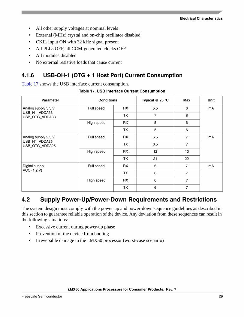
4.1.6 USB-OH-1 (OTG + 1 Host Port) Current ConsumptionTable 17 shows the USB interface current consumption.
4.2 Supply Power-Up/Power-Down Requirements and RestrictionsThe system design must comply with the power-up and power-down sequence guidelines as described in this section to guarantee reliable operation of the device. Any deviation from these sequences can result in the following situations:
• Excessive current during power-up phase
• Prevention of the device from booting
• Irreversible damage to the i.MX50 processor (worst-case scenario)
Table 17. USB Interface Current Consumption
Parameter Conditions Typical @ 25 °C Max Unit
Analog supply 3.3 VUSB_H1_VDDA33USB_OTG_VDDA33
Full speed RX 5.5 6 mA
TX 7 8
High speed RX 5 6
TX 5 6
Analog supply 2.5 VUSB_H1_VDDA25USB_OTG_VDDA25
Full speed RX 6.5 7 mA
TX 6.5 7
High speed RX 12 13
TX 21 22
Digital supplyVCC (1.2 V)
Full speed RX 6 7 mA
TX 6 7
High speed RX 6 7
TX 6 7

i.MX50 Applications Processors for Consumer Products, Rev. 7
Electrical Characteristics
Freescale Semiconductor30
4.2.1 Power-Up SequenceFigure 2 shows the power-up sequence.
Figure 2. Power-Up Sequence
NOTE1) The POR_B input must be immediately asserted at power-up and remain asserted until after the last power rail is at its working voltage.
2) No power-up sequence dependencies exist between the supplies shown shaded in gray.
4.2.2 Power-Down Sequence
The power-down sequence is recommended to be the opposite of the power-up sequence. In other words, the same power supply constraints exist while powering off as while powering on.
4.2.3 Resume Sequence
When the i.MX50 is resuming from STOP mode, there are some special sequencing considerations. The resume timing is determined by the following internal counters:
1. STBY_COUNT. This register is in the CCM block and may be set to a maximum of 16 x 32 kHz cycles, or 500 μsec.

Electrical Characteristics
i.MX50 Applications Processors for Consumer Products, Rev. 7
Freescale Semiconductor 31
2. OSCNT. This register is in the CCM block and may be set to a maximum of 256 x 32 kHz cycles, or 8 msec. This counter is intended to give the 24MHz clock time to start up and stabilize.
If the PMIC_RDY input is used and BYPASS_PMIC_VFUNCTIONAL_READY = 0, the i.MX50 will wait for STBY_COUNT cycles after PMIC_STBY_REQ negation before checking PMIC_RDY status. Once the STBY_COUNT has expired AND the PMIC_RDY signal has been asserted, the OSCNT counter begins and the 24MHz oscillator is powered up. After OSCNT expires the processor will enter RUN mode.
If the PMIC_RDY input is not used, the processor will attempt to start the 24 MHz oscillator after STBY_COUNT expires. So at a minimum, all the supplies necessary to start up the 24 MHz oscillator need to be powered before STBY_COUNT expires: NVCC_SRTC,VDD1P2, VDD1P8, VDD2P5, VDD3P0. After STBY_COUNT expires, the OSCNT counter begins and the 24 MHz oscillator is powered up. After OSCNT expires the processor will enter RUN mode, so all other supplies need to be at the appropriate operating levels before OSCNT expires.
4.3 I/O DC ParametersThis section includes the DC parameters of the following I/O types:
• General Purpose I/O and High-Speed General Purpose I/O (GPIO)
• Double Data Rate 2 (DDR2)
• Low Power Double Data Rate 2 (LPDDR2)
• Low Power Double Data Rate 1(LPDDR1)
• Low Voltage I/O (LVIO)
• High Voltage I/O (HVIO)
• Secure Digital Host Controllers (eSDHCv2 and eSDHCv3)
• USB-OTG and USB Host ports
NOTEThe term OVDD in this section refers to the associated supply rail of an input or output.
4.3.1 GPIO I/O DC ParametersThe parameters in Table 18 are guaranteed per the operating ranges in Table 11, unless otherwise noted.
Table 18. GPIO DC Electrical Characteristics
DC Electrical Characteristics Symbol Test Conditions MIN Typ MAX Units
High-level output voltage Voh Ioh=-1mAIoh=spec’ed Drive
OVDD-0.150.8*OVDD
— — V
Low-level output voltage Vol Iol=1mAIol=specified Drive
— — 0.150.2*OVDD
V
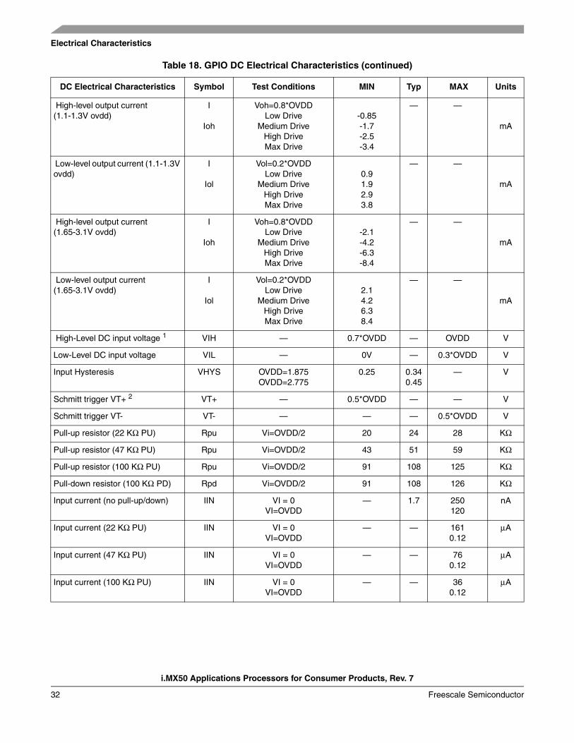
i.MX50 Applications Processors for Consumer Products, Rev. 7
Electrical Characteristics
Freescale Semiconductor32
High-level output current (1.1-1.3V ovdd)
I
Ioh
Voh=0.8*OVDDLow Drive
Medium DriveHigh DriveMax Drive
-0.85-1.7-2.5-3.4
— —
mA
Low-level output current (1.1-1.3V ovdd)
I
Iol
Vol=0.2*OVDDLow Drive
Medium DriveHigh DriveMax Drive
0.91.92.93.8
— —
mA
High-level output current (1.65-3.1V ovdd)
I
Ioh
Voh=0.8*OVDDLow Drive
Medium DriveHigh DriveMax Drive
-2.1-4.2-6.3-8.4
— —
mA
Low-level output current (1.65-3.1V ovdd)
I
Iol
Vol=0.2*OVDDLow Drive
Medium DriveHigh DriveMax Drive
2.14.26.38.4
— —
mA
High-Level DC input voltage 1 VIH — 0.7*OVDD — OVDD V
Low-Level DC input voltage VIL — 0V — 0.3*OVDD V
Input Hysteresis VHYS OVDD=1.875OVDD=2.775
0.25 0.340.45
— V
Schmitt trigger VT+ 2 VT+ — 0.5*OVDD — — V
Schmitt trigger VT- VT- — — — 0.5*OVDD V
Pull-up resistor (22 KΩ PU) Rpu Vi=OVDD/2 20 24 28 KΩ
Pull-up resistor (47 KΩ PU) Rpu Vi=OVDD/2 43 51 59 KΩ
Pull-up resistor (100 KΩ PU) Rpu Vi=OVDD/2 91 108 125 KΩ
Pull-down resistor (100 KΩ PD) Rpd Vi=OVDD/2 91 108 126 KΩ
Input current (no pull-up/down) IIN VI = 0VI=OVDD
— 1.7 250120
nA
Input current (22 KΩ PU) IIN VI = 0VI=OVDD
— — 1610.12
μA
Input current (47 KΩ PU) IIN VI = 0VI=OVDD
— — 760.12
μA
Input current (100 KΩ PU) IIN VI = 0VI=OVDD
— — 360.12
μA
Table 18. GPIO DC Electrical Characteristics (continued)
DC Electrical Characteristics Symbol Test Conditions MIN Typ MAX Units

Electrical Characteristics
i.MX50 Applications Processors for Consumer Products, Rev. 7
Freescale Semiconductor 33
4.3.2 DDR2 I/O DC Parameters
The DDR2 interface fully complies with JESD79-2E DDR2 JEDEC standard release April, 2008. The JEDEC LPDDR2 specification (JESD209_2B) supersedes any specification in this document. The parameters in Table 19 are guaranteed per the operating ranges in Table 11, unless otherwise noted.
Input current (100 KΩ PD) IIN VI = 0VI=OVDD
— — 0.2536
μA
External pull-up / pull-downresistor required to overdriveinternal keeper
Rext — — — 47 KΩ
1 To maintain a valid level, the transitioning edge of the input must sustain a constant slew rate (monotonic) from the current DC level through to the target DC level, VIL or VIH. Monotonic input transition time is from 0.1ns to 1s. VIL and VIH do not apply when hysteresis is enabled.
2 Hysteresis of 250 mV is guaranteed overall operating conditions when hysteresis is enabled.
Table 19. DDR2 DC Electrical Characteristics
DC Electrical Characteristics SymbolTest
ConditionsMIN TYP MAX Units
High-level output voltage Voh — 0.9*ovdd — — V
Low-level output voltage Vol — — — 0.1*ovdd V
Output min source current1
1 ovdd=1.7 V; Vout=1.42 V. (Vout-ovdd)/Ioh must be less than 21 Ω for values of Vout between ovdd and ovdd-0.28 V.
Ioh(dc) — -7.5 — — mA
Output min sink current2
2 ovdd=1.7 V; Vout=280 mV. Vout/Iol must be less than 21 Ω for values of Vout between 0 V and 280 mV.
Iol(dc) — 7.5 — — mA
Input reference voltage Vref — 0.49*ovdd 0.5*ovdd 0.51*ovdd —
DC input high voltage (data pins) Vihd(dc) — Vref+0.125 — ovdd+0.3 V
DC input low voltage (data pins) Vild(dc) — -0.3 — Vref-0.125 V
DC input voltage3 (clk pins)
3 Vin(dc) specifies the allowable dc excursion of each differential input.
Vin(dc) — -0.3 — ovdd+0.3 V
DC differential input voltage4
4 Vid(dc) specifies the input differential voltage |Vtr-Vcp| required for switching, where Vtr is the “pure” input level and Vcp is the “complementary” input level. the minimum value is equal to Vih(dc) - Vil(dc).
Vid(dc) — 0.25 — ovdd+0.6 V
Termination voltage5
5 Vtt is expected to track ovdd/2.
Vtt — Vref-0.04 Vref Vref+0.04 —
Input current6 (no pull-up/down)
6 Typ condition: typ model, 1.8 V, and 25 °C. Max condition: BCS model, 1.9 V, and 125 °C. Min condition: WCS model, 1.7 V, and -40 °C.
Iin VI = 0VI=ovdd
— 0.072
5360
nA
Tri-state I/O supply current6 Icc-ovdd VI = ovdd or 0 — 2.3 480 nA
Tri-state 2.5V predrivers supply current6
Icc-vdd2p5 VI = ovdd or 0 — 6.4 750 nA
Tri-state core supply current6 Icc-vddi VI = ovdd or 0 — 3.1 720 nA
Table 18. GPIO DC Electrical Characteristics (continued)
DC Electrical Characteristics Symbol Test Conditions MIN Typ MAX Units

i.MX50 Applications Processors for Consumer Products, Rev. 7
Electrical Characteristics
Freescale Semiconductor34
4.3.3 Low Power DDR2 I/O DC ParametersThe LPDDR2 interface fully complies with JEDEC standard release April, 2008. The parameters in Table 20 are guaranteed per the operating ranges in Table 11, unless otherwise noted.
4.3.4 Low Power DDR1 I/O DC Parameters
The LPDDR1 interface fully complies with JEDEC standard release April, 2008. The parameters in Table 21 are guaranteed per the operating ranges in Table 11, unless otherwise noted.
Table 20. LPDDR2 I/O DC Electrical Parameters
DC Electrical Characteristics Symbol Test Conditions MIN TYP MAX Units
High-level output voltage Voh — 0.9*ovdd — — V
Low-level output voltage Vol — — — 0.1*ovdd V
Input reference voltage Vref — 0.49*ovdd 0.5*ovdd 0.51*ovdd —
DC input high voltage Vih(dc) — Vref+0.13 — ovdd V
DC input low voltage Vil(dc) — ovss — Vref-0.13 V
Differential input logic high1
1 The single-ended signals need to be within the respective limits (Vih(dc) max, Vil(dc) min) for single-ended signals as well as the limitations for overshoot and undershoot.
Vih(diff) — 0.26 — — V
Differential input logic low1 Vil(diff) — — — -0.26 V
Input current (no pull-up/down) Iin VI = 0VI=ovdd
— 0.021.5
12.8290
nA
Tri-state I/O supply current2
2 Typ condition: typ model, 1.2V, and 25 °C. Max condition: BCS model, 1.3V, and 125 °C. Min condition: WCS model, 1.14V, and -40 °C.
Icc-ovdd VI = ovdd or 0 — 1.85 400 nA
Tri-state 2.5 V predrivers supply current2
Icc-vdd2p5 VI = ovdd or 0 — 5 700 nA
Tri-state core supply current2 Icc-vddi VI = ovdd or 0 — 3 700 nA
Pullup/Pulldown impedance mismatch2
— — -15 — +15 %
240 Ω unit calibration resolution — — — — 10 Ω
Table 21. LPDDR1 Mode DC Electrical Characteristics
DC Electrical Characteristics Symbol Test Conditions MIN TYP MAX Units
High-level output voltage Voh Ioh=-0.1mA 0.9*ovdd — — V
Low-level output voltage Vol Iol=0.1mA — — 0.1*ovdd V
DC input high voltage (data pins) Vihd(dc) — 0.7*ovdd — ovdd+0.3 V
DC input low voltage (data pins) Vild(dc) — -0.3 — 0.3*ovdd V
DC input voltage1 (clk pins) Vin(dc) — -0.3 — ovdd+0.3 V
DC input differential voltage2 Vid(dc) — 0.4*ovdd — ovdd+0.6 V
Input current3 (no pull-up/down) Iin VI = 0VI=ovdd
— 0.072
5360
nA
Tri-state I/O supply current3 Icc-ovdd VI = ovdd or 0 — 2.3 480 nA
Tri-state 2.5V predrivers supply current3
Icc-vdd2p5
VI = ovdd or 0 — 5.3 680 nA
Tri-state core supply current3 Icc-vddi VI = ovdd or 0 — 3.1 720 nA

Electrical Characteristics
i.MX50 Applications Processors for Consumer Products, Rev. 7
Freescale Semiconductor 35
4.3.5 Low Voltage I/O (LVIO) DC ParametersThe parameters in Table 22 are guaranteed per the operating ranges in Table 11, unless otherwise noted.
1 Vin(dc) specifies the allowable dc excursion of each differential input.2 Vid(dc) specifies the input differential voltage |Vtr-Vcp| required for switching, where Vtr is the “pure” input level and Vcp is
the “complementary” input level. the minimum value is equal to Vih(dc) - Vil(dc).3 Typ condition: typ model, 1.8 V, and 25 °C. Max condition: BCS model, 1.9 V, and 105 °C. Min condition: WCS model, 1.7 V,
and -20 °C.
Table 22. LVIO DC Electrical Characteristics
DC Electrical Characteristics Symbol Test Conditions MIN Typ MAX Units
High-level output voltage Voh Ioh=-1mAIoh=spec’ed Drive
OVDD-0.150.8*OVDD
— — V
Low-level output voltage Vol Iol=1mAIol=specified Drive
— — 0.150.2*OVDD
V
High-level output current I
Ioh
Voh=0.8*OVDDLow Drive
Medium DriveHigh DriveMax Drive
-2.1-4.2-6.3-8.4
— —
mA
Low-level output current I
Iol
Vol=0.2*OVDDLow Drive
Medium DriveHigh DriveMax Drive
2.14.26.38.4
— —
mA
High-Level DC input voltage 1 VIH — 0.7*OVDD — OVDD V
Low-Level DC input voltage VIL — 0V — 0.3*OVDD V
Input Hysteresis VHYS OVDD=1.875OVDD=2.775
0.35 0.621.27
— V
Schmitt trigger VT+ 2 VT+ — 0.5*OVDD — — V
Schmitt trigger VT- VT- — — — 0.5*OVDD V
Pull-up resistor (22 KΩ PU) Rpu Vi=OVDD/2 20 24 28 KΩ
Pull-up resistor (47 KΩ PU) Rpu Vi=OVDD/2 43 51 59 KΩ
Pull-up resistor (100 KΩ PU) Rpu Vi=OVDD/2 91 108 125 KΩ
Pull-down resistor (100 KΩ PD) Rpd Vi=OVDD/2 91 108 126 KΩ
Input current (no pull-up/down) IIN VI = 0VI=OVDD
— 1.7 250120
nA
Input current (22 KΩ PU) IIN VI = 0VI=OVDD
— — 1610.12
μA
Input current (47 KΩ PU) IIN VI = 0VI=OVDD
— — 760.12
μA
Input current (100 KΩ PU) IIN VI = 0VI=OVDD
— — 360.12
μA

i.MX50 Applications Processors for Consumer Products, Rev. 7
Electrical Characteristics
Freescale Semiconductor36
4.3.6 High Voltage I/O (HVIO) DC ParametersTable 23 shows the HVIO DC electrical operating conditions. The parameters are guaranteed per the operating ranges in Table 11, unless otherwise noted.
Input current (100 KΩ PD) IIN VI = 0VI=OVDD
— — 0.2536
μA
External pull-up / pull-downresistor required to overdriveinternal keeper
Rext — — — 47 KΩ
1 To maintain a valid level, the transitioning edge of the input must sustain a constant slew rate (monotonic) from the current DC level through to the target DC level, VIL or VIH. Monotonic input transition time is from 0.1 ns to 1 s. VIL and VIH do not apply when hysteresis is enabled.
2 Hysteresis of 350 mV is guaranteed over all operating conditions when hysteresis is enabled.
Table 23. HVIO DC Electrical Characteristics
DC Electrical Characteristics Symbol Test Conditions MIN TYP MAX Units
High-level output voltage Voh Ioh=-1mAIoh=spec’ed Drive
OVDD-0.150.8*OVDD
— — V
Low-level output voltage Vol Iol=1mAIol=specified Drive
— — 0.150.2*OVDD
V
High-level output current, low voltage mode Ioh_lv
Voh=0.8*OVDDLow Drive
Medium DriveHigh Drive
-2.2-4.4-6.6
— —
mA
High-level output current, high voltage mode Ioh_hv
Vol=0.8*OVDDLow Drive
Medium DriveHigh Drive
-5.1-10.2-15.3
— —
mA
Low-level output current, low voltage modeIol_lv
Voh=0.2*OVDDLow Drive
Medium DriveHigh Drive
2.24.46.6
— —
mA
Low-level output current, high voltage mode Iol_hv
Voh=0.2*OVDDLow Drive
Medium DriveHigh Drive
5.110.215.3
— —
mA
High-Level DC input voltage1 VIH — 0.7*OVDD — OVDD V
Low-Level DC input voltage VIL — 0V — 0.3*OVDD V
Input Hysteresis VHYS OVDD=1.875OVDD=3.0
0.25 0.360.80
— V
Schmitt trigger VT+2 VT+ — 0.5*OVDD — — V
Schmitt trigger VT- VT- — — — 0.5*OVDD V
Table 22. LVIO DC Electrical Characteristics (continued)
DC Electrical Characteristics Symbol Test Conditions MIN Typ MAX Units

Electrical Characteristics
i.MX50 Applications Processors for Consumer Products, Rev. 7
Freescale Semiconductor 37
4.4 Output Buffer Impedance CharacteristicsThis section defines the I/O impedance parameters of the i.MX50 processor.
Pull-up resistor (22 KΩ PU) Rpu Vi=OVDD/2 22 29 71 KΩ
Pull-up resistor (47 KΩ PU) Rpu Vi=OVDD/2 43 59 148 KΩ
Pull-up resistor (100 KΩ PU) Rpu Vi=OVDD/2 46 62 156 KΩ
Pull-down resistor (100 KΩ PD) Rpd Vi=OVDD/2 53 77 256 KΩ
Input current (no pull-up/down) IIN VI = 0VI=OVDD
— 2.8 47050
nA
Input current (22 KΩ PU) IIN VI = 0VI=OVDD
— — 1530.05
μA
Input current (47 KΩ PU) IIN VI = 0VI=OVDD
— — 770.05
μA
Input current (100 KΩ PU) IIN VI = 0VI=OVDD
— — 730.05
μA
Input current (100 KΩ PD) IIN VI = 0VI=OVDD
— — 0.4763
μA
High-level output current, high voltage mode Ioh_hv
Vol=0.8*OVDDLow Drive
Medium DriveHigh Drive
-5.1-10.2-15.3
— —
mA
External pull-up / pull-downresistor required to overdriveinternal keeper
Rext — — — 2.5 KΩ
1 To maintain a valid level, the transitioning edge of the input must sustain a constant slew rate (monotonic) from the current DC level through to the target DC level, VIL or VIH. Monotonic input transition time is from 0.1 ns to 1 s. VIL and VIH do not apply when hysteresis is enabled.
2 Hysteresis of 250 mV is guaranteed over all operating conditions when hysteresis is enabled.
Table 23. HVIO DC Electrical Characteristics (continued)
DC Electrical Characteristics Symbol Test Conditions MIN TYP MAX Units

i.MX50 Applications Processors for Consumer Products, Rev. 7
Electrical Characteristics
Freescale Semiconductor38
4.4.1 GPIO Output Buffer ImpedanceTable 24 shows the GPIO output buffer impedance of the i.MX50 processor.
4.4.2 LVIO Output Buffer ImpedanceTable 25 shows the LVIO output buffer impedance of the i.MX50 processor.
Table 24. GPIO Output Buffer Impedance
Parameter Symbol Test Conditions Min
Typ
Max UnitOVDD
2.775 VOVDD1.875V
Output driver impedance
Rpu Low drive strength, Ztl = 150 ΩMedium drive strength, Ztl = 75 ΩHigh drive strength, Ztl = 50 ΩMax drive strength, Ztl = 37.5 Ω
80402720
104523526
150755138
2501258362
Ω
Output driver impedance
Rpd Low drive strength, Ztl = 150 ΩMedium drive strength, Ztl = 75 ΩHigh drive strength, Ztl = 50 ΩMax drive strength, Ztl = 37.5 Ω
64322116
88443022
134664434
2431228161
Ω
Table 25. LVIO Output Buffer Impedance
Parameter Symbol Test Conditions Min
Typ
Max UnitOVDD
2.775 VOVDD1.875V
Output driver impedance
Rpu Low drive strength, Ztl = 150 ΩMedium drive strength, Ztl = 75 ΩHigh drive strength, Ztl = 50 ΩMax drive strength, Ztl = 37.5 Ω
80402720
104523526
150755138
2501258362
Ω
Output driver impedance
Rpd Low drive strength, Ztl = 150 ΩMedium drive strength, Ztl = 75 ΩHigh drive strength, Ztl = 50 ΩMax drive strength, Ztl = 37.5 Ω
64322116
88443022
134664434
2431228161
Ω

Electrical Characteristics
i.MX50 Applications Processors for Consumer Products, Rev. 7
Freescale Semiconductor 39
4.4.3 HVIO Output Buffer ImpedanceTable 26 shows the HVIO output buffer impedance of the i.MX50 processor.
NOTEOutput driver impedance is measured with long transmission line of impedance Ztl attached to I/O pad and incident wave launched into transmission line. Rpu/Rpd and Ztl form a voltage divider that defines specific voltage of incident wave relative to OVDD. Output driver impedance is calculated from this voltage divider (see Figure 3).
Table 26. HVIO Output Buffer Impedance
Parameter Symbol Test Conditions
Min Typ Max
UnitOVDD1.95 V
OVDD3.3 V
OVDD1.875 V
OVDD3.30V
OVDD1.65 V
OVDD2.68 V
Output driver impedance
Rpu Low drive strength, Ztl = 150 ΩMedium drive strength, Ztl = 75 ΩHigh drive strength, Ztl = 50 Ω
113.556.237.8
103.851.935.1
130.666
45.9
13369.241
219.4109.773.1
212.2111.171.8
Ω
Output driver impedance
Rpd Low drive strength, Ztl =1 50 ΩMedium drive strength, Ztl = 75 ΩHigh drive strength, Ztl = 50 Ω
78.539.726.8
7034.523
113.656.838.3
10250
33.3
230.8115.476.9
179.589.860.7
Ω

i.MX50 Applications Processors for Consumer Products, Rev. 7
Electrical Characteristics
Freescale Semiconductor40
Figure 3. Impedance Matching Load for Measurement
ipp_do
Cload = 1p
Ztl W, L = 20 inches
Predriver
PMOS (Rpu)
NMOS (Rpd)
Pad
OVDD
OVSS
t,(ns)0
U,(V)
OVDD
t,(ns)0
VDDVin (do)
Vout (pad)U,(V)
Vref
Rpu = Vovdd – Vref1
Vref1× Ztl
Rpd = × ZtlVref2
Vovdd – Vref2
Vref1 Vref2

Electrical Characteristics
i.MX50 Applications Processors for Consumer Products, Rev. 7
Freescale Semiconductor 41
4.5 I/O AC ParametersThe load circuit and output transition time waveforms are shown in Figure 4 and Figure 5. The AC electrical characteristics for slow and fast I/O are presented in the Table 27 and Table 28, respectively. Note that the fast or slow I/O behavior is determined by the appropriate control bit in the IOMUX control registers.
Figure 4. Load Circuit for Output
Figure 5. Output Transition Time Waveform
4.5.1 GPIO I/O Slow AC Parameters Table 27 shows the AC parameters for GPIO slow I/O.
Table 27. GPIO I/O Slow AC Parameters
Parameter Symbol Test Condition Min Typ Max Unit
Output Pad Transition Times (Max Drive) tr, tf 15 pF35 pF
1.91/1.523.07/2.65
ns
Output Pad Transition Times (High Drive) tr, tf 15 pF35 pF
2.22/1.813.81/3.42
ns
Output Pad Transition Times (Medium Drive) tr, tf 15 pF35 pF
2.88/2.425.43/5.02
ns
Output Pad Transition Times (Low Drive) tr, tf 15 pF35 pF
4.94/4.5010.55/9.70
ns
Output Pad Slew Rate (Max Drive)1 tps 15 pF35 pF
0.5/0.650.32/0.37
V/ns
Output Pad Slew Rate (High Drive) tps 15 pF35 pF
0.43/0.540.26/0.41
V/ns
Output Pad Slew Rate (Medium Drive) tps 15 pF35 pF
0.34/0.410.18/0.2
V/ns
Output Pad Slew Rate (Low Drive) tps 15 pF35 pF
0.20/0.220.09/0.1
V/ns
Output Pad di/dt (Max Drive) tdit 30 mA/ns
Test pointFrom output
CL
CL includes package, probe and fixture capacitance
Under test
0V
NVCC
20%
80% 80%
20%
tr tfOutput (at I/O)

i.MX50 Applications Processors for Consumer Products, Rev. 7
Electrical Characteristics
Freescale Semiconductor42
4.5.2 GPIO I/O Fast AC Parameters
Table 28 shows the AC parameters for GPIO fast I/O.
Output Pad di/dt (High Drive) tdit 23 mA/ns
Output Pad di/dt (Medium drive) tdit 15 mA/ns
Output Pad di/dt (Low drive) tdit 7 mA/ns
Input Transition Times2 trm 25 ns
1 tps is measured between VIL to VIH for rising edge and between VIH to VIL for falling edge.2 Hysteresis mode is recommended for inputs with transition time greater than 25 ns.
Table 28. GPIO I/O Fast AC Parameters
Parameter Symbol Test Condition Min Typ Max Unit
Output Pad Transition Times (Max Drive) tr, tf 15 pF35 pF
1.45/1.242.76/2.54
ns
Output Pad Transition Times (High Drive)
tr, tf 15 pF35 pF
1.81/1.593.57/3.33
ns
Output Pad Transition Times (Medium Drive)
tr, tf 15 pF35 pF
2.54/2.295.25/5.01
ns
Output Pad Transition Times (Low Drive) tr, tf 15 pF35 pF
4.82/4.5010.54/9.95
ns
Output Pad Slew Rate (Max Drive)1
1 tps is measured between VIL to VIH for rising edge and between VIH to VIL for falling edge.
tps 15 pF35 pF
0.69/0.780.36/0.39
V/ns
Output Pad Slew Rate (High Drive) tps 15 pF35 pF
0.55/0.620.28/0.30
V/ns
Output Pad Slew Rate (Medium Drive) tps 15 pF35 pF
0.39/0.440.19/0.20
V/ns
Output Pad Slew Rate (Low Drive) tps 15 pF35 pF
0.21/0.220.09/0.1
V/ns
Output pad di/dt (Max drive) tdit — — — 70 mA/ns
Output pad di/dt (High drive) tdit — — — 53 mA/ns
Output pad di/dt (Medium drive) tdit — — — 35 mA/ns
Output pad di/dt (Low drive) tdit — — — 18 mA/ns
Input transition times2
2 Hysteresis mode is recommended for inputs with transition time greater than 25 ns.
trm — — — 25 ns
Table 27. GPIO I/O Slow AC Parameters (continued)
Parameter Symbol Test Condition Min Typ Max Unit

Electrical Characteristics
i.MX50 Applications Processors for Consumer Products, Rev. 7
Freescale Semiconductor 43
4.5.3 LVIO I/O Slow AC Parameters Table 27 shows the AC parameters for LVIO slow I/O.
Table 29. LVIO I/O Slow AC Parameters
Parameter Symbol Test Condition Min Typ Max Unit
Output Pad Transition Times (Max Drive) tr, tf 15 pF35 pF
1.97/1.573.12/2.70
ns
Output Pad Transition Times (High Drive) tr, tf 15 pF35 pF
2.29/1.873.79/3.44
ns
Output Pad Transition Times (Medium Drive) tr, tf 15 pF35 pF
2.93/2.485.42/4.98
ns
Output Pad Transition Times (Low Drive) tr, tf 15 pF35 pF
4.92/4.5710.64/9.85
ns
Output Pad Slew Rate (Max Drive)1
1 tps is measured between VIL to VIH for rising edge and between VIH to VIL for falling edge.
tps 15 pF35 pF
0.50/0.630.32/0.37
V/ns
Output Pad Slew Rate (High Drive) tps 15 pF35 pF
0.43/0.530.26/0.29
V/ns
Output Pad Slew Rate (Medium Drive) tps 15 pF35 pF
0.34/0.400.18/0.20
V/ns
Output Pad Slew Rate (Low Drive) tps 15 pF35 pF
0.20/0.220.09/0.10
V/ns
Output Pad di/dt (Max Drive) tdit 30 mA/ns
Output Pad di/dt (High Drive) tdit 24 mA/ns
Output Pad di/dt (Medium drive) tdit 16 mA/ns
Output Pad di/dt (Low drive) tdit 8 mA/ns
Input Transition Times2
2 Hysteresis mode is recommended for inputs with transition time greater than 25 ns.
trm 25 ns

i.MX50 Applications Processors for Consumer Products, Rev. 7
Electrical Characteristics
Freescale Semiconductor44
4.5.4 LVIO I/O Fast AC ParametersTable 30 shows the AC parameters for LVIO fast I/O.
4.5.5 HVIO I/O Low Voltage (1.8 V) AC Parameters Table 27 shows the AC parameters for HVIO I/O Low Voltage (1.8 V).
Table 30. LVIO I/O Fast AC Parameters
Parameter Symbol Test Condition Min Typ Max Unit
Output Pad Transition Times (Max Drive) tr, tf 15 pF35 pF
1.44/1.272.78/2.56
ns
Output Pad Transition Times (High Drive)
tr, tf 15 pF35 pF
1.80/1.613.59/3.34
ns
Output Pad Transition Times (Medium Drive)
tr, tf 15 pF35 pF
2.55/2.285.32/5.01
ns
Output Pad Transition Times (Low Drive) tr, tf 15 pF35 pF
4.74/4.5910.59/10.21
ns
Output Pad Slew Rate (Max Drive)1
1 tps is measured between VIL to VIH for rising edge and between VIH to VIL for falling edge.
tps 15 pF35 pF
0.69/0.780.36/0.39
V/ns
Output Pad Slew Rate (High Drive) tps 15 pF35 pF
0.55/0.610.28/0.30
V/ns
Output Pad Slew Rate (Medium Drive) tps 15 pF35 pF
0.39/0.440.19/0.20
V/ns
Output Pad Slew Rate (Low Drive) tps 15 pF35 pF
0.21/0.220.09/0.10
V/ns
Output pad di/dt (Max drive) tdit — — — 70 mA/ns
Output pad di/dt (High drive) tdit — — — 54 mA/ns
Output pad di/dt (Medium drive) tdit — — — 35 mA/ns
Output pad di/dt (Low drive) tdit — — — 18 mA/ns
Input transition times2
2 Hysteresis mode is recommended for inputs with transition time greater than 25 ns.
trm — — — 25 ns
Table 31. HVIO I/O Low Voltage (1.8 V) AC Parameters
Parameter Symbol Test Condition Min Typ Max Unit
Output Pad Transition Times (High Drive) tr, tf 15 pF35 pF
1.82/1.973.39/3.57
ns
Output Pad Transition Times (Medium Drive) tr, tf 15 pF35 pF
2.48/2.624.95/5.14
ns
Output Pad Transition Times (Low Drive) tr, tf 15 pF35 pF
4.57/4.779.60/9.91
ns

Electrical Characteristics
i.MX50 Applications Processors for Consumer Products, Rev. 7
Freescale Semiconductor 45
4.5.6 HVIO I/O High Voltage (3.0 V) AC ParametersTable 32 shows the AC parameters for HVIO I/O High Voltage (3.0 V).
Output Pad Slew Rate (High Drive)1 tr, tf 15 pF35 pF
0.54/0.500.29/0.28
V/ns
Output Pad Slew Rate (Medium Drive) tr, tf 15 pF35 pF
0.40/0.380.20/0.19
V/ns
Output Pad Slew Rate (Low Drive) tr, tf 15 pF35 pF
0.22/0.210.10/0.10
V/ns
Output Pad di/dt (High Drive) tdit 34 mA/ns
Output Pad di/dt (Medium drive) tdit 22 mA/ns
Output Pad di/dt (Low drive) tdit 11 mA/ns
Input Transition Times2 trm 25 ns
1 tps is measured between VIL to VIH for rising edge and between VIH to VIL for falling edge.2 Hysteresis mode is recommended for inputs with transition time greater than 25 ns.
Table 32. HVIO I/O High Voltage (3.0 V) AC Parameters
Parameter Symbol Test Condition Min Typ Max Unit
Output Pad Transition Times (High Drive)
tpr 15 pF35 pF
2.16/1.793.75/3.28
ns
Output Pad Transition Times (Medium Drive)
tpr 15 pF35 pF
2.81/2.405.06/4.58
ns
Output Pad Transition Times (Low Drive) tpr 15 pF35 pF
4.69/4.158.91/8.51
ns
Output Pad Slew Rate (High Drive)1
1 tps is measured between VIL to VIH for rising edge and between VIH to VIL for falling edge.
tps 15 pF35 pF
0.75/0.900.43/0.49
V/ns
Output Pad Slew Rate (Medium Drive) tps 15 pF35 pF
0.57/0.670.32/0.35
V/ns
Output Pad Slew Rate (Low Drive) tps 15 pF35 pF
0.34/0.390.18/0.19
V/ns
Output pad di/dt (High drive) tdit — — — 55 mA/ns
Output pad di/dt (Medium drive) tdit — — — 36 mA/ns
Output pad di/dt (Low drive) tdit — — — 16 mA/ns
Input transition times2
2 Hysteresis mode is recommended for inputs with transition time greater than 25 ns.
trm — — — 25 ns
Table 31. HVIO I/O Low Voltage (1.8 V) AC Parameters (continued)
Parameter Symbol Test Condition Min Typ Max Unit

i.MX50 Applications Processors for Consumer Products, Rev. 7
Electrical Characteristics
Freescale Semiconductor46
4.5.7 DDR2 I/O AC ParametersTable 33 shows the AC parameters for DDR2 I/O.
Table 33. DDR2 I/O AC Parameters
Parameter Symbol Min Max Unit
AC input logic high Vih(ac) Vref+0.25 -
V
AC input logic low Vil(ac) - Vref-0.25
AC differential input voltage1
1Vid(ac) specifies the input differential voltage |Vtr-Vcp| required for switching, where Vtr is the“true” input signal and Vcp is the “complementary” input signal. The Minimum value is equal toVih(ac)-Vil(ac)
Vid(ac) 0.5 ovdd
AC Input differential cross point voltage2
2The typical value of Vix(ac) is expected to be about 0.5*OVDD. and Vix(ac) is expected to trackvariation of OVDD. Vix(ac) indicates the voltage at which differential input signal must cross.
Vix(ac) 0.5*ovdd -0.175
0.5*ovdd + 0.175
AC output differential cross point voltage 3
3The typical value of Vox(ac) is expected to be about 0.5*OVDD and Vox(ac) is expected to trackvariation in OVDD. Vox(ac) indicates the voltage at which differential output signal must cross.
Vox(ac) 0.5*ovdd -0.125
0.5*ovdd+ 0.125
Output propagation delay high to low tPOHLD 3.5
nsOutput propagation delay low to high tPOLHD 3.5
Input propagation delay high to low tPIHLD 1.5
Input propagation delay low to high tPILHD 1.5
Single output slew rate tsr 0.4 2 V/ns

Electrical Characteristics
i.MX50 Applications Processors for Consumer Products, Rev. 7
Freescale Semiconductor 47
4.5.8 LPDDR1 I/O AC ParametersTable 34 shows the AC parameters for LPDDR1 I/O.
4.5.9 LPDDR2 I/O AC ParametersTable 35 shows the AC parameters for LPDDR2 I/O.
Table 34. LPDDR1 I/O AC Parameters
Parameter Symbol Min Max Unit
AC input logic high Vihd(ac) 0.8*ovdd ovdd+0.3
V
AC input logic low Vild(ac) -0.3 0.2*ovdd
AC input differential voltage1
1Vid(ac) specifies the input differential voltage |Vtr-Vcp| required for switching, where Vtr isthe “true” input signal and Vcp is the “complementary” input signal. The Minimum value isequal to Vih(ac)-Vil(ac)
Vid(ac) 0.6*ovdd ovdd+0.6
AC input differential crosspoint voltage2
2The typical value of Vix(ac) is expected to be about 0.5*ovdd. and Vix(ac) is expected totrack variation of ovdd. Vix(ac) indicates the voltage at which differential input signal mustcross.
Vix(ac) 0.4*ovdd 0.6*ovdd
Output propagation delay high to low tPOHLD 2.5ns
Output propagation delay low to high tPOLHD 2.5
Input propagation delay high to low tPIHLD 1.5
Input propagation delay low to high tPILHD 1.5
Single output slew rate tsr 0.3 2.5 V/ns
Table 35. LPDDR2 I/O AC Parameters
Parameter Symbol Min Max Unit
AC input logic high Vih(ac) Vref+0.22 ovdd
V
AC input logic low Vil(ac) ovss Vref-0.22
AC differential input high voltage1 Vidh(ac) 0.44 -
AC differential input low voltage Vidhl(ac) - 0.44
AC input differential cross point voltage (relative to ovdd / 2)2
Vix(ac) -0.12 0.12
Over/undershoot peak Vpeak 0.35ns
Over/undershoot area (above OVDD or below OVSS)
Varea 0.6 (at 266 MHz)
V-ns
Output propagation delay high to low tPOHLD 3.5ns
Output propagation delay low to high tPOLHD 3.5
Input propagation delay high to low tPIHLD 1.5
Input propagation delay low to high tPILHD 1.5

i.MX50 Applications Processors for Consumer Products, Rev. 7
Electrical Characteristics
Freescale Semiconductor48
4.6 System Modules TimingThis section contains the timing and electrical parameters for the modules in the i.MX50 processor.
4.6.1 Reset Timings ParametersFigure 6 shows the reset timing and Table 36 lists the timing parameters.
Figure 6. Reset Timing Diagram
4.6.2 WDOG Reset Timing ParametersFigure 7 shows the WDOG reset timing and Table 37 lists the timing parameters.
Figure 7. WDOG_RST_B Timing Diagram
Single output slew rate(Driver impedance =40Ω+/-30%)
tsr 1.5 3.5 V/ns
Single output slew rate(Driver impedance =60Ω+/-30%
tsr 1 2.5 V/ns
1Vid(ac) specifies the input differential voltage |Vtr-Vcp| required for switching, where Vtr is the“true” input signal and Vcp is the “complementary” input signal. The Minimum value is equal toVih(ac)-Vil(ac).2The typical value of Vix(ac) is expected to be about 0.5*OVDD. and Vix(ac) is expected to trackvariation of OVDD. Vix(ac) indicates the voltage at which differential input signal must cross.
Table 36. Reset Timing Parameters
ID Parameter Min Max Unit
CC1 Duration of RESET_IN_B assertion to be qualified as valid (input slope = 5 ns)
50 — ns
Table 35. LPDDR2 I/O AC Parameters (continued)
Parameter Symbol Min Max Unit
RESET_IN_B
CC1
(Input)
WDOG_RST_B
CC5
(Input)

Electrical Characteristics
i.MX50 Applications Processors for Consumer Products, Rev. 7
Freescale Semiconductor 49
NOTECKIL is approximately 32 kHz. TCKIL is one period or approximately 30 μs.
4.6.3 Clock Amplifier Parameters (CKIH)
The input to clock amplifier (CAMP) is internally ac-coupled allowing direct interface to a square wave or sinusoidal frequency source. No external series capacitors are required.
Table 38 shows the electrical parameters of CAMP.
4.6.4 DPLL Electrical ParametersTable 39 shows the electrical parameters of digital phase-locked loop (DPLL).
Table 37. WDOG_RST_B Timing Parameters
ID Parameter Min Max Unit
CC5 Duration of WDOG_RST_B Assertion 1 — TCKIL
Table 38. CAMP Electrical Parameters (CKIH)
Parameter Min Typ Max Unit
Input frequency 8.0 — 40.0 MHz
VIL (for square wave input) 0 — 0.3 V
VIH (for square wave input) (VCC1 – 0.25)
1 VCC is the supply voltage of CAMP.
— 3 V
Sinusoidal input amplitude 0.4 2
2 This value of the sinusoidal input is determined during characterization.
— VDD Vp-p
Output duty cycle 45 50 55 %
Table 39. DPLL Electrical Parameters
Parameter Test Conditions/Remarks Min Typ Max Unit
Reference clock frequency range1 — 10 — 100 MHz
Reference clock frequency range after pre-divider
— 10 — 40 MHz
Output clock frequency range (dpdck_2) — 300 — 1025 MHz
Pre-division factor2 — 1 — 16 —
Multiplication factor integer part — 5 — 15 —
Multiplication factor numerator3 Should be less than denominator –67108862 — 67108862 —
Multiplication factor denominator2 — 1 — 67108863 —
Output duty cycle — 48.5 50 51.5 %

i.MX50 Applications Processors for Consumer Products, Rev. 7
Electrical Characteristics
Freescale Semiconductor50
4.6.5 General Purpose Media Interface (GPMI) ParametersThe i.MX50 GPMI controller is a flexible interface NAND Flash controller with 8-bit data width, up to 200 MB/s I/O speed and individual chip select.
It supports Asynchronous timing mode, Source Synchronous timing mode and Samsung Toggle timing mode separately described in the following paragraphs.
4.6.5.1 Asynchronous Mode AC Timing (ONFI 1.0 Compatible)
Asynchronous mode AC timings are provided as multiplications of the clock cycle and fixed delay. The Maximum I/O speed of GPMI in Asynchronous mode is about 50 MB/s. Figure 8, Figure 9, Figure 10 and Figure 11 depict the relative timing between GPMI signals at the module level for different
Frequency lock time4
(FOL mode or non-integer MF)— — — 398 Tdpdref
Phase lock time — — — 100 µs
Frequency jitter5 (peak value) — — 0.02 0.04 Tdck
Phase jitter (peak value) FPL mode, integer and fractional MF — 2.0 3.5 ns
Power dissipation fdck = 300 MHz @ avdd = 1.8 V, dvdd = 1.2 Vfdck = 650 MHz @ avdd = 1.8 V, dvdd = 1.2 V
— — 0.65 (avdd)0.92 (dvdd)1.98 (avdd)1.8 (dvdd)
mW
1 Device input range cannot exceed the electrical specifications of the CAMP, see Table 38.2 The values specified here are internal to DPLL. Inside the DPLL, a 1 is added to the value specified by the user. Therefore, the
user has to enter a value 1 less than the desired value at the inputs of DPLL for PDF and MFD.3 The maximum total multiplication factor (MFI + MFN/MFD) allowed is 15. Therefore, if the MFI value is 15, MFN value must be
zero.4 Tdpdref is the time period of the reference clock after predivider. According to the specification, the maximum lock time in FOL
mode is 398 cycles of divided reference clock when DPLL starts after full reset.5 Tdck is the time period of the output clock, dpdck_2.
Table 39. DPLL Electrical Parameters (continued)
Parameter Test Conditions/Remarks Min Typ Max Unit

Electrical Characteristics
i.MX50 Applications Processors for Consumer Products, Rev. 7
Freescale Semiconductor 51
operations under Asynchronous mode. Table 40 describes the timing parameters (NF1–NF17) that are shown in the figures.
Figure 8. Command Latch Cycle Timing Diagram
Figure 9. Address Latch Cycle Timing Diagram
CLE
CEn
WE
ALE
IO[7:0] Command
NF9NF8
NF1 NF2
NF5
NF3 NF4
NF6 NF7
CLE
CEn
WE
ALE
IO[7:0] Address
NF9NF8
NF1
NF5
NF3 NF4
NF6
NF11
NF10
NF7
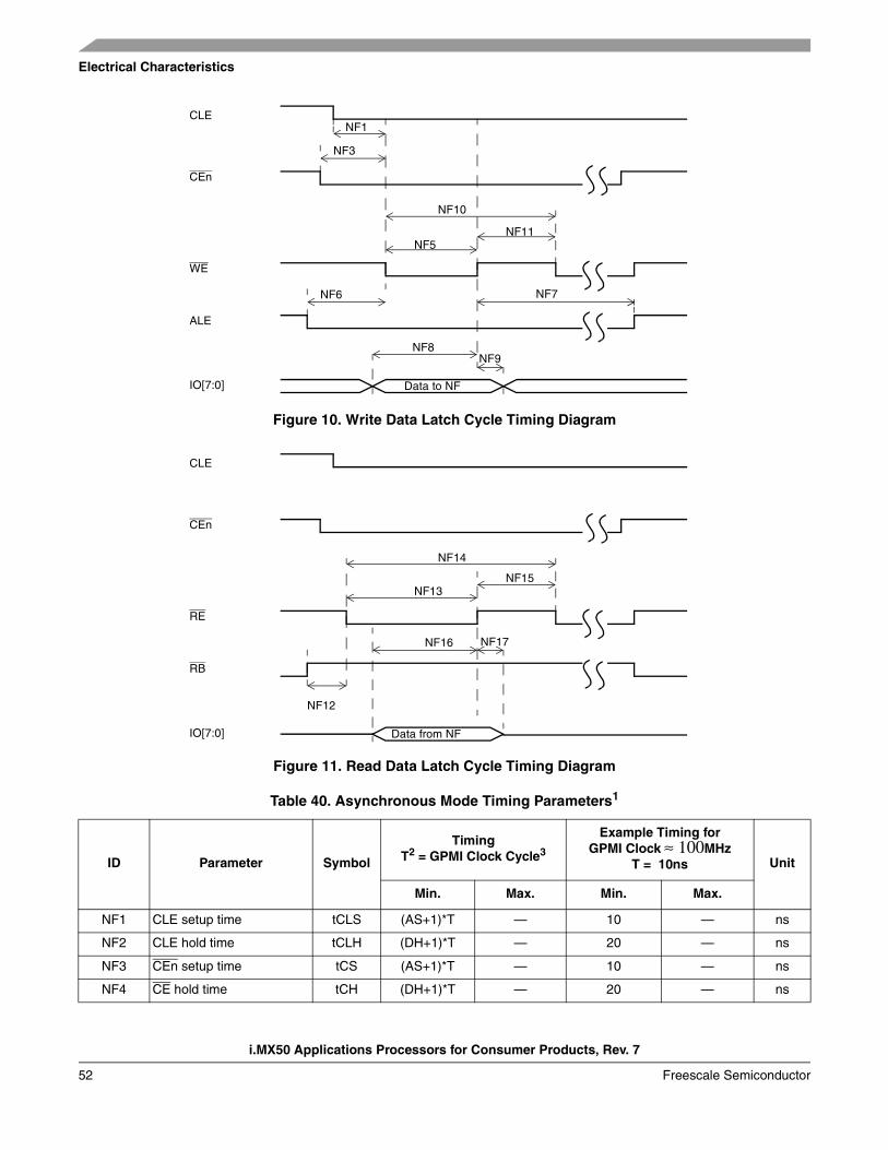
i.MX50 Applications Processors for Consumer Products, Rev. 7
Electrical Characteristics
Freescale Semiconductor52
Figure 10. Write Data Latch Cycle Timing Diagram
Figure 11. Read Data Latch Cycle Timing Diagram
Table 40. Asynchronous Mode Timing Parameters1
ID Parameter Symbol
TimingT2 = GPMI Clock Cycle3
Example Timing for GPMI Clock ≈ 100MHz
T = 10ns Unit
Min. Max. Min. Max.
NF1 CLE setup time tCLS (AS+1)*T — 10 — ns
NF2 CLE hold time tCLH (DH+1)*T — 20 — ns
NF3 CEn setup time tCS (AS+1)*T — 10 — ns
NF4 CE hold time tCH (DH+1)*T — 20 — ns
CLE
CEn
WE
ALE
IO[7:0] Data to NF
NF9NF8
NF1
NF5
NF3
NF6
NF11
NF10
NF7
CLE
CEn
RE
RB
IO[7:0] Data from NF
NF13NF15
NF14
NF17
NF12
NF16

Electrical Characteristics
i.MX50 Applications Processors for Consumer Products, Rev. 7
Freescale Semiconductor 53
NF5 WE pulse width tWP DS*T 10 ns
NF6 ALE setup time tALS (AS+1)*T — 10 — ns
NF7 ALE hold time tALH (DH+1)*T — 20 — ns
NF8 Data setup time tDS DS*T — 10 — ns
NF9 Data hold time tDH DH*T — 10 — ns
NF10 Write cycle time tWC (DS+DH)*T 20 ns
NF11 WE hold time tWH DH*T 10 ns
NF12 Ready to RE low tRR (AS+1)*T — 10 — ns
NF13 RE pulse width tRP DS*T — 10 — ns
NF14 READ cycle time tRC (DS+DH)*T — 20 — ns
NF15 RE high hold time tREH DH*T 10 — ns
NF16 Data setup on read tDSR N/A 10 — ns
NF17 Data hold on read tDHR N/A 10 — ns1 GPMI’s Async Mode output timing could be controlled by module’s internal register, say
HW_GPMI_TIMING0_ADDRESS_SETUP, HW_GPMI_TIMING0_DATA_SETUP, and HW_GPMI_TIMING0_DATA_HOLD. This AC timing depends on these registers’ setting. In the above table, we use AS/DS/DH representing these settings each.
2 T represents for the GPMI clock period.3 AS minimum value could be 0, while DS/DH minimum value is 1.
Table 40. Asynchronous Mode Timing Parameters1 (continued)
ID Parameter Symbol
TimingT2 = GPMI Clock Cycle3
Example Timing for GPMI Clock ≈ 100MHz
T = 10ns Unit
Min. Max. Min. Max.

i.MX50 Applications Processors for Consumer Products, Rev. 7
Electrical Characteristics
Freescale Semiconductor54
4.6.5.2 Source Synchronous Mode AC Timing (ONFI 2.x Compatible)
The following diagrams show the write and read timing of Source Synchronous Mode.
Figure 12. Source Synchronous Mode Command and Address Timing Diagram
CE_N
CLE
ALE
CLK
DQS
W/R#
DQ[7:0] CMD
NF20NF21
NF22
NF23
NF18NF19
DQS outputenable
DQ[7:0] Outputenable
NF24
ADD ADD
NF20NF21

Electrical Characteristics
i.MX50 Applications Processors for Consumer Products, Rev. 7
Freescale Semiconductor 55
Figure 13. Source Synchronous Mode Data Write Timing Diagram
CE_N
CLE
ALE
CLK
DQS
W/R#
DQ[7:0]
NF22
NF23
NF18NF19
DQS outputenable
DQ[7:0] Outputenable
NF24
NF27 NF27NF27
NF25
NF25
NF26

i.MX50 Applications Processors for Consumer Products, Rev. 7
Electrical Characteristics
Freescale Semiconductor56
Figure 14. Source Synchronous Mode Data Read Timing Diagram
Table 41. Source Synchronous Mode Timing Parameters1
ID Parameter Symbol
TimingT = GPMI Clock Cycle Unit
Min. Max.
NF18 CE# access time tCE CE_DELAY*tCK — ns
NF19 CE# hold time tCH 0.5 *tCK — ns
NF20 Command/address DQ setup time
tCAS 0.5*tCK — ns
NF21 Command/address DQ hold time
tCAH 0.5*tCK — ns
NF22 clock period tCK 5 — ns
NF23 preamble delay tPRE PRE_DELAY*tCK — ns
CE_N
CLE
ALE
CLK
DQS
W/R#
DQ[7:0]
NF22
NF23
NF18NF19
DQS output enable
DQ[7:0] Outputenable
NF24
NF25NF25
NF25 NF26

Electrical Characteristics
i.MX50 Applications Processors for Consumer Products, Rev. 7
Freescale Semiconductor 57
4.6.5.3 Samsung Toggle Mode AC Timing
4.6.5.3.1 Command and Address Timing
NOTESamsung Toggle Mode command and address timing is the same as ONFI 1.0 compatible Async mode AC timing. Please refer to the above chapter for details.
NF24 postamble delay tPOST POST_DELAY*tCK — ns
NF25 CLE and ALE setup time tCALS 0.5*tCK — ns
NF26 CLE and ALE hold time tCALH 0.5*tCK — ns
NF27 Data input to first DQS latching transition
tDQSS tCK — ns
1 GPMI’s sync mode output timing could be controlled by module’s internal register, say HW_GPMI_TIMING2_CE_DELAY, HW_GPMI_TIMING_PREAMBLE_DELAY, and HW_GPMI_TIMING2_POST_DELAY. This AC timing depends on these registers’ setting. In the above table, we use CE_DELAY/PRE_DELAY/POST_DELAY representing these settings each.
Table 41. Source Synchronous Mode Timing Parameters1 (continued)
ID Parameter Symbol
TimingT = GPMI Clock Cycle Unit
Min. Max.

i.MX50 Applications Processors for Consumer Products, Rev. 7
Electrical Characteristics
Freescale Semiconductor58
4.6.5.3.2 Read and Write Timing
Figure 15. Samsung Toggle Mode Data Write Timing
CE_N
CLE
ALE
WE_N
DQS
RE_N
DQ[7:0]
NF23
0.5 tCK
NF22
NF24
0.5 tCK
0
0
0
1
1
dev_clk

Electrical Characteristics
i.MX50 Applications Processors for Consumer Products, Rev. 7
Freescale Semiconductor 59
Figure 16. Samsung Toggle Mode Data Read Timing
Table 42. Samsung Toggle Mode Timing Parameters1
ID Parameter Symbol
TimingT = GPMI Clock Cycle Unit
Min. Max.
NF18 CE# access time tCE CE_DELAY*tCK — ns
NF19 CE# hold time tCH 0.5 *tCK — ns
NF20 Command/address DQ setup time
tCAS 0.5*tCK — ns
NF21 Command/address DQ hold time
tCAH 0.5*tCK — ns
NF22 clock period tCK 7.5 — ns
CE_N
CLE
ALE
WE_N
DQS
RE_N
DQ[7:0]
NF23
NF24
0
0
11 tCK
1 tCK
1 tCK
NF18
dev_clk
1 tCK1 tCK

i.MX50 Applications Processors for Consumer Products, Rev. 7
Electrical Characteristics
Freescale Semiconductor60
4.7 External Interface Module (EIM)The following sections provide information on the EIM.
4.7.1 General EIM TimingFigure 17, Figure 18, and Table 43 specify the timings related to the EIM module. All EIM output control signals may be asserted and de-asserted by an internal clock synchronized to the EIM_BCLK rising edge according to corresponding assertion/negation control fields.
,
Figure 17. EIM Outputs Timing Diagram
NF23 preamble delay tPRE (PRE_DELAY+1)*tCK — ns
NF24 postamble delay tPOST POST_DELAY*tCK — ns
NF25 CLE and ALE setup time tCALS 0.5*tCK — ns
NF26 CLE and ALE hold time tCALH 0.5*tCK — ns1 GPMI’s sync mode output timing could be controlled by module’s internal register, say HW_GPMI_TIMING2_CE_DELAY,
HW_GPMI_TIMING_PREAMBLE_DELAY, HW_GPMI_TIMING2_POST_DELAY. This AC timing depends on these registers’ setting. In the above table, we use CE_DELAY/PRE_DELAY/POST_DELAY representing these settings each.
Table 42. Samsung Toggle Mode Timing Parameters1 (continued)
ID Parameter Symbol
TimingT = GPMI Clock Cycle Unit
Min. Max.
WE4EIM_ADDR
EIM_CSx
EIM_RW
EIM_OE
EIM_BCLK
EIM_EBx
EIM_LBA
EIM_DATA
...
WE5
WE6 WE7
WE8 WE9
WE10 WE11
WE12 WE13
WE14 WE15
WE16 WE17
WE3WE2WE1

Electrical Characteristics
i.MX50 Applications Processors for Consumer Products, Rev. 7
Freescale Semiconductor 61
Figure 18. EIM Inputs Timing Diagram
EIM_DATA
EIM_WAIT
EIM_BCLK
WE19
WE18
WE21
WE20

i.MX50 Applications Processors for Consumer Products, Rev. 7
Electrical Characteristics
Freescale Semiconductor62
Table 43. EIM Bus Timing Parameters 1
1 t is axi_clk cycle time. The maximum allowed axi_clk frequency is 133 MHz, whereas the maximum allowed EIM_BCLK frequency is 66.5 MHz. As a result, if BCD = 0, axi_clk must be ≤ 66.5 MHz. If BCD = 1, then 133 MHz is allowed for axi_clk, resulting in a EIM_BCLK of 66.5 MHz. When the clock branch to EIM is decreased to 66.5 MHz, other buses are impacted which are clocked from this source. See the CCM chapter of the MCIMX50 Applications Processor Reference Manual (MCIMX50RM) for a detailed clock tree description.
ID ParameterBCD = 0 BCD = 1 BCD = 2 BCD = 3
Min Max Min Max Min Max Min Max
WE1 EIM_BCLK Cycle time2 t — 2t — 3t — 4t —
WE2 EIM_BCLK Low Level Width 0.4t — 0.8t — 1.2t — 1.6t —
WE3 EIM_BCLK High Level Width
0.4t — 0.8t — 1.2t — 1.6t —
WE4 Clock rise to address valid3 0.5t – 1.25 0.5t + 1.75 t – 1.25 t + 1.75 2t – 1.25 2t + 1.75 3t – 1.25 3t + 1.75
WE5 Clock rise to address invalid 0.5t – 1.25 0.5t + 1.75 t – 1.25 t + 1.75 2t – 1.25 2t + 1.75 3t – 1.25 3t + 1.75
WE6 Clock rise to EIM_CSx valid 0.5t – 1.25 0.5t + 1.75 t – 1.25 t + 1.75 2t – 1.25 2t + 1.75 3t – 1.25 3t + 1.75
WE7 Clock rise to EIM_CSx invalid
0.5t – 1.25 0.5t + 1.75 t – 1.25 t + 1.75 2t – 1.25 2t + 1.75 3t – 1.25 3t + 1.75
WE8 Clock rise to EIM_RW valid 0.5t – 1.25 0.5t + 1.75 t – 1.25 t + 1.75 2t – 1.25 2t + 1.75 3t – 1.25 3t + 1.75
WE9 Clock rise to EIM_RW invalid
0.5t – 1.25 0.5t + 1.75 t – 1.25 t + 1.75 2t – 1.25 2t + 1.75 3t – 1.25 3t + 1.75
WE10 Clock rise to EIM_OE valid 0.5t – 1.25 0.5t + 1.75 t – 1.25 t + 1.75 2t – 1.25 2t + 1.75 3t – 1.25 3t + 1.75
WE11 Clock rise to EIM_OE invalid 0.5t – 1.25 0.5t + 1.75 t – 1.25 t + 1.75 2t – 1.25 2t + 1.75 3t – 1.25 3t + 1.75
WE12 Clock rise to EIM_EBx valid 0.5t – 1.25 0.5t + 1.75 t – 1.25 t + 1.75 2t – 1.25 2t + 1.75 3t – 1.25 3t + 1.75
WE13 Clock rise to EIM_EBx invalid
0.5t – 1.25 0.5t + 1.75 t – 1.25 t + 1.75 2t – 1.25 2t + 1.75 3t – 1.25 3t + 1.75
WE14 Clock rise to EIM_LBA valid 0.5t – 1.25 0.5t + 1.75 t – 1.25 t + 1.75 2t – 1.25 2t + 1.75 3t – 1.25 3t + 1.75
WE15 Clock rise to EIM_LBA invalid
0.5t – 1.25 0.5t + 1.75 t – 1.25 t + 1.75 2t – 1.25 2t + 1.75 3t – 1.25 3t + 1.75
WE16 Clock rise to Output Data valid
0.5t – 1.25 0.5t + 1.75 t – 1.25 t + 1.75 2t – 1.25 2t + 1.75 2t – 1.25 2t + 1.75
WE17 Clock rise to Output Data Invalid
0.5t – 1.25 0.5t + 1.75 t – 1.25 t + 1.75 2t – 1.25 2t + 1.75 2t – 1.25 2t + 1.75
WE18 Input Data setup time to Clock rise
2 — 2 — 2 — 2 —
WE19 Input Data hold time from Clock rise
2.5 — 2.5 — 2.5 — 2.5 —
WE20 EIM_WAIT setup time to Clock rise
2 — 2 — 2 — 2 —
WE21 EIM_WAIT hold time from Clock rise
2.5 — 2.5 — 2.5 — 2.5 —

Electrical Characteristics
i.MX50 Applications Processors for Consumer Products, Rev. 7
Freescale Semiconductor 63
4.7.2 Examples of EIM AccessesFigure 19, Figure 20, Figure 21, Figure 22, Figure 23, and Figure 24 give a few examples of basic EIM accesses to external memory devices with the timing parameters mentioned previously for specific control parameters settings.
Figure 19. Synchronous Memory Read Access, WSC=1
2 EIM_BCLK parameters are being measured from the 50% point that is, high is defined as 50% of signal value and low is defined as 50% as signal value.
3 For signal measurements High is defined as 80% of signal value and Low is defined as 20% of signal value.
Last Valid Address Address v1
D(v1)
EIM_BCLK
EIM_ADDR
EIM_DATA
EIM_RW
EIM_LBA
EIM_OE
EIM_EBx
EIM_CSx
Next AddressWE4 WE5
WE6 WE7
WE10 WE11
WE13WE12
WE14 WE15
WE18
WE19

i.MX50 Applications Processors for Consumer Products, Rev. 7
Electrical Characteristics
Freescale Semiconductor64
Figure 20. Synchronous Memory, Write Access, WSC=1, WBEA=1, WBEN=1, and WADVN=0
Figure 21. Synchronous 16-Bit Memory, Two Non-Sequential 32-Bit Read Accesses, WSC=2, SRD=1, BCD=0
Last Valid Address Address V1
D(V1)
EIM_BCLK
EIM_ADDR
EIM_DATA
EIM_RW
EIM_LBA
EIM_OE
EIM_EBx
EIM_CSx
Next Address
WE4 WE5
WE6 WE7
WE8 WE9
WE12 WE13
WE14
WE15
WE16 WE17
Last Valid Addr Address V1 Address V2
D(V1) D(V1+1) D(V2) D(V2+1)
EIM_BCLK
EIM_ADDR
EIM_WAIT
EIM_DATA Halfword Halfword
EIM_CSx
EIM_RW
EIM_LBA
EIM_OE
EIM_EBx
Halfword Halfword
WE4 WE5
WE7
WE10 WE11
WE12 WE13
WE14WE15
WE18
WE19WE20
WE21
WE6
WE15 WE14

Electrical Characteristics
i.MX50 Applications Processors for Consumer Products, Rev. 7
Freescale Semiconductor 65
Figure 22. Synchronous Memory, Burst Write, BCS=1, WSC=4, SRD=1, and BCD=0
Figure 23. Muxed Address/Data (A/D) Mode, Synchronous Write Access, WSC=6,ADVA=1, ADVN=1, and ADH=1
NOTEIn 32-bit muxed address/data (A/D) mode, the 16 MSBs are driven on the data bus.
Last Valid Addr
EIM_BCLK
EIM_ADDR
EIM_DATA
EIM_CSx
EIM_RW
EIM_LBA
EIM_OE
EIM_EBx
EIM_WAIT
Address V1
D(V1) D(V2) D(V4)D(V3)
WE12
WE4 WE5
WE6 WE7
WE8 WE9
WE13
WE14
WE16 WE16
WE17WE17
WE20
WE21
WE15
Last
EIM_BCLK
EIM_ADDR/
EIM_RW
EIM_LBA
EIM_OE
EIM_EBx
EIM_CSx
Address V1 Write DataValid AddrEIM_DATA
WE4 WE16
WE6 WE7
WE9WE8
WE10 WE11
WE14 WE15
WE17WE5

i.MX50 Applications Processors for Consumer Products, Rev. 7
Electrical Characteristics
Freescale Semiconductor66
Figure 24. 16-Bit Muxed A/D Mode, Synchronous Read Access, WSC=7, RADVN=1, ADH=1, OEA=2
Figure 25, Figure 26, Figure 27, and Table 44 help to determine timing parameters relative to the chip select (CS) state for asynchronous and DTACK EIM accesses with corresponding EIM bit fields and the timing parameters mentioned above.
Figure 25. Asynchronous Memory Read Access
Last
EIM_BCLK
EIM_ADDR/
EIM_RW
EIM_LBA
EIM_OE
EIM_EBx
EIM_CSx
Address V1 DataValid AddrEIM_DATA
WE5
WE6
WE7
WE14 WE15
WE10 WE11
WE12 WE13
WE18
WE19WE4
Last Valid Address Address V1
D(V1)
EIM_ADDR
EIM_DATA
EIM_RW
EIM_LBA
EIM_OE
EIM_EBx
EIM_CSx
Next Address
WE39
WE35
WE37
WE32
WE36
WE38
WE43
WE40
WE31
WE44

Electrical Characteristics
i.MX50 Applications Processors for Consumer Products, Rev. 7
Freescale Semiconductor 67
Figure 26. Asynchronous Memory Write Access
Figure 27. DTACK Read Access
Table 44. EIM Asynchronous Timing Parameters Table Relative Chip Select
ID ParameterDetermination by
Synchronous Measured Parameters 1
Min Max Unit
WE31 EIM_CSx valid to Address valid WE4 – WE6 – CSA2 — 3 – CSA ns
WE32 Address invalid to EIM_CSx invalid WE7 – WE5 – CSN3 — 3 – CSN ns
WE33 EIM_CSx valid to EIM_RW valid WE8 – WE6 + (WEA – CSA) — 3 + (WEA – CSA) ns
Last Valid Address Address V1
D(V1)
EIM_ADDR
EIM_DATA
EIM_RW
EIM_LBA
EIM_OE
EIM_EBx
EIM_CSx
Next Address
WE31
WE39
WE33
WE45
WE32
WE40
WE34
WE46
WE42
WE41
Last Valid Address Address V1
D(V1)
EIM_ADDR
EIM_DATA
EIM_RW
EIM_LBA
EIM_OE
EIM_EBx
EIM_CSx
Next Address
WE39
WE35
WE37
WE32
WE36
WE38
WE43
WE40
WE31
WE44
EIM_DTACK
WE48
WE47

i.MX50 Applications Processors for Consumer Products, Rev. 7
Electrical Characteristics
Freescale Semiconductor68
4.8 DRAM Timing Parameters
This section includes descriptions of the electrical specifications of DRAM MC module which interfaces external DDR2, LPDDR1, and LPDDR2 memory devices.
WE34 EIM_RW invalid to EIM_CSx invalid WE7 – WE9 + (WEN – CSN) — 3 – (WEN_CSN) ns
WE35 EIM_CSx valid to EIM_OE valid WE10 – WE6 + (OEA – CSA) — 3 + (OEA – CSA) ns
WE36 EIM_OE invalid to EIM_CSx invalid WE7 – WE11 + (OEN – CSN) — 3 – (OEN – CSN) ns
WE37 EIM_CSx valid to EIM_EBx valid (Read access)
WE12 – WE6 + (RBEA – CSA) — 3 + (RBEA4 – CSA) ns
WE38 EIM_EBx invalid to EIM_CSx invalid (Read access)
WE7 – WE13 + (RBEN – CSN) — 3 – (RBEN5 – CSN) ns
WE39 EIM_CSx valid to EIM_LBA valid WE14 – WE6 + (ADV – CSA) — 3 + (ADVA – CSA) ns
WE40 EIM_LBA invalid to EIM_CSx invalid (ADVL is asserted)
WE7 – WE15 – CSN — 3 – CSN ns
WE41 EIM_CSx valid to Output Data valid WE16 – WE6 – WCSA — 3 – WCSA ns
WE42 Output Data invalid to EIM_CSx invalid
WE17 – WE7 – CSN — 3 – CSN ns
WE43 Input Data valid to EIM_CSx invalid MAXCO + MAXDI MAXCO6 + MAXDI7
— ns
WE44 EIM_CSx invalid to Input Data invalid 0 0 — ns
WE45 EIM_CSx valid to EIM_EBx valid (Write access)
WE12 – WE6 + (WBEA – CSA) — 3 + (WBEA – CSA) ns
WE46 EIM_EBx invalid to EIM_CSx invalid (Write access)
WE7 – WE13 + (WBEN – CSN) — –3 + (WBEN – CSN) ns
WE47 EIM_DTACK valid to EIM_CSx invalid
MAXCO + MAXDTI MAXCO6 + MAXDTI8
— ns
WE48 EIM_CSx invalid to EIM_DTACK invalid
0 0 — ns
1 Parameters WE4–WE21 value, see in the Table 44.2 EIM_CSx Assertion. This bit field determines when EIM_CSx signal is asserted during read/write cycles.3 EIM_CSx Negation. This bit field determines when EIM_CSx signal is negated during read/write cycles.4 EIM_EBx Assertion. This bit field determines when EIM_EBx signal is asserted during read cycles.5 EIM_EBx Negation. This bit field determines when EIM_EBx signal is negated during read cycles.6 Output maximum delay from internal driving the FFs to chip outputs. The maximum delay between all memory controls
(EIM_ADDR, EIM_CSx, EIM_OE, EIM_RW, EIM_EBx, and EIM_LBA).7 Maximum delay from chip input data to internal FFs. The maximum delay between all data input pins.8 DTACK maximum delay from chip input data to internal FF.
Table 44. EIM Asynchronous Timing Parameters Table Relative Chip Select (continued)
ID ParameterDetermination by
Synchronous Measured Parameters 1
Min Max Unit

Electrical Characteristics
i.MX50 Applications Processors for Consumer Products, Rev. 7
Freescale Semiconductor 69
4.8.1 DRAM Command & Address Output Timing—DDR2 and LPDDR1The following diagrams and tables specify the timings related to the address and command pins, which interfaces DDR2 and LPDDR1 memory devices.
Table 45. EMI Command/Address AC Timing
ID Description Symbol Min Max Unit
DDR1 CK cycle time tCK 3.75 — ns
DDR2 CK high level width tCH 0.48 tCK 0.52 tCK ns
DDR3 CK low level width tCL 0.48 tCK 0.52 tCK ns
DDR4 Address and control output setup time tIS 0.5 tCK- 0.3
— ns
DDR5 Address and control output hold time tIH 0.5 tCK- 0.3
— ns
Figure 28. DRAM Command/Address Output Timing—DDR2 and LPDDR1
DRAM_SDCLK
DRAM_SDCLK_B
DRAM_CS0
DRAM_RAS
DRAM_CAS
DRAM_SDWE
bankrow
bankcolumn
DRAM_ADDR
DDR1
DDR2 DDR3
DDR4 DDR5
DDR4 DDR5
DDR4
DDR5

i.MX50 Applications Processors for Consumer Products, Rev. 7
Electrical Characteristics
Freescale Semiconductor70
4.8.2 DRAM Command and Address Output Timing—LPDDR2The following diagrams and tables specify the timings related to the address and command pins, which interface LPDDR2 memory devices.
Table 46. EMI Command/Address AC Timing
ID Description Symbol Min Max Unit
DDR1 CK cycle time tCK 3.75 — ns
DDR2 CK high level width tCH 0.48 tCK 0.52 tCK ns
DDR3 CK low level width tCL 0.48 tCK 0.52 tCK ns
DDR4 Control output setup time tIS 0.5 tCK- 0.3
— ns
DDR5 Control output hold time tIH 0.5 tCK- 0.3
— ns
DDR6CK >= 200 MHz
Address output setup time tIS 0.5 tCK- 1.3
— ns
DDR7CK >= 200 MHz
Address output hold time tIH 0.5 tCK- 1.3
— ns
DDR6CK < 200 MHz
Address output setup time tIS 1 — ns
DDR7CK < 200 MHz
Address output hold time tIH 1 — ns
Figure 29. DRAM Command/Address Output Timing—LPDDR2
DRAM_SDCLK
DRAM_SDCLK_B
DRAM_CS0
DRAM_A[9:0]
DDR1
DDR2 DDR3
DDR4 DDR5
rise fall
DDR6
DDR7

Electrical Characteristics
i.MX50 Applications Processors for Consumer Products, Rev. 7
Freescale Semiconductor 71
NOTEDDR6 and DDR7 can be adjusted by the parameter -DLL_WR_DELAY-;
The ideal case is that SDCLK is center aligned to the DRAM_A[9:0] data valid window;
For this table, HW_DRAM_PHY23[14:8] (DLL_WR_DELAY) = 0x10;
4.8.3 DRAM Data Output TimingThe DRAM data output timing is defined for all DDR types: DDR2, LPDDR1, and LPDDR2.
Table 47. DDR Output AC Timing
ID Description Symbol Min Max Unit
DDR10 Positive DQS latching edge to associated CK edge tDQSS -0.3 0.3 ns
DDR11 DQS falling edge from CK rising edge—hold time tDSH 0.5 tCK- 0.3
0.5 tCK+ 0.3
ns
DDR12 DQS falling edge to CK rising edge—setup time tDSS 0.5 tCK- 0.3
0.5 tCK+ 0.3
ns
DDR13 DQS output high pulse width tDQSH 0.48 tCK 0.52 tCK ns
DDR14 DQS output low pulse width tDQSL 0.48 tCK 0.52 tCK ns
DDR15CK >= 200 MHz
DQ & DQM output setup time relative to DQS tDS 0.5 tCK- 1.3
— ns
Figure 30. DRAM Data Output Timing
DRAM_SDCLK
DRAM_SDCLK_B
DRAM_SDQS
DDR13 DDR14
d0
DDR10
d1 d2 d3DRAM_D &DRAM_DQM
DDR11 DDR12
DDR15
DDR16
DRAM_SDQS_B

i.MX50 Applications Processors for Consumer Products, Rev. 7
Electrical Characteristics
Freescale Semiconductor72
NOTEThe DDR15,16 could be adjusted by the parameter “DLL_WR_DELAY”;
The ideal case is that SDQS is center aligned to the DRAM_D data valid window;
For this table, HW_DRAM_PHY15[14:8] (DLL_WR_DELAY) = 0x10;
4.8.4 DRAM Data Input TimingDRAM Data input timing is defined for all DDR types: DDR2, LPDDR1, and LPDDR2.
DDR16CK >= 200 MHz
DQ & DQM output hold time relative to DQS tDH 0.5 tCK- 1.3
— ns
DDR15CK < 200 MHz
DQ & DQM output setup time relative to DQS tDS 1 — ns
DDR16CK < 200 MHz
DQ & DQM output hold time relative to DQS tDH 1 — ns
Table 48. DDR2 Input AC Timing
ID Description Symbol Min Max Unit
DDR20 Positive DQS latching edge to associated CK edge tDQSCK -0.5 tCK — ns
Table 47. DDR Output AC Timing
ID Description Symbol Min Max Unit
Figure 31. DRAM Data Input Timing
DRAM_SDCLK
DRAM_SDCLK_B
DRAM_SDQS
DDR21
DDR22
d0
DDR20
d1 d2 d3DRAM_D
DRAM_SDQS_B

Electrical Characteristics
i.MX50 Applications Processors for Consumer Products, Rev. 7
Freescale Semiconductor 73
NOTEThe timing parameter DDR20(tDQSCK) is not strictly required by this DRAM MC design.
4.9 External Peripheral InterfacesThe following sections provide information on external peripheral interfaces.
4.9.1 AUDMUX Timing Parameters
The AUDMUX provides programmable interconnect logic for voice, audio and data routing between internal serial interfaces (SSIs) and external serial interfaces (audio and voice codecs). The AC timing of AUDMUX external pins is hence governed by the SSI module.
4.9.2 CSPI and eCSPI Timing ParametersThis section describes the timing parameters of the CSPI and eCSPI modules. The CSPI and eCSPI have separate timing parameters for master and slave modes. The nomenclature used with the CSPI/eCSPI modules and the respective routing of these signals is shown in Table 49.
DDR21 DQS to DQ input skew tDQSQ — 0.65 ns
DDR22 DQS to DQ input hold time tQH 0.45 tCK-0.85
— ns
Table 49. CSPI Nomenclature and Routing
Module I/O Access
eCSPI1 GPIO, KPP, DISP0_DAT, CSI0_DAT, and EIM_D through IOMUX
eCSPI2 DISP0_DAT, CSI0_DAT, and EIM through IOMUX
CSPI DISP0_DAT, EIM_A/D, SD1, and SD2 through IOMUX
Table 48. DDR2 Input AC Timing
ID Description Symbol Min Max Unit

i.MX50 Applications Processors for Consumer Products, Rev. 7
Electrical Characteristics
Freescale Semiconductor74
4.9.2.1 CSPI Master Mode Timing
Figure 32 depicts the timing of CSPI in master mode and Table 50 lists the CSPI master mode timing characteristics.
Figure 32. CSPI Master Mode Timing Diagram
Table 50. CSPI Master Mode Timing Parameters
ID Parameter Symbol Min Max Unit
CS1 CSPIx_CLK Cycle Time tclk 60 — ns
CS2 CSPIx_CLK High or Low Time tSW 6 — ns
CS3 CSPIx_CLK Rise or Fall tRISE/FALL — — ns
CS4 CSPIx_CS_x pulse width tCSLH 15 — ns
CS5 CSPIx_CS_x Lead Time (CS setup time) tSCS 5 — ns
CS6 CSPIx_CS_x Lag Time (CS hold time) tHCS 5 — ns
CS7 CSPIx_DO Setup Time tSmosi 5 — ns
CS8 CSPIx_DO Hold Time tHmosi 5 — ns
CS9 CSPIx_DI Setup Time tSmiso 5 — ns
CS10 CSPIx_DI Hold Time tHmiso 5 — ns
CS11 CSPIx_DRYN Setup Time tSDRY 5 — ns
CS1
CS7 CS8
CS2
CS2
CS4
CS6 CS5
CS9 CS10
CSPIx_CLK
CSPIx_CS_x
CSPIx_DO
CSPIx_DI
CSPIx_DRYN1
CS11
CS3
CS3

Electrical Characteristics
i.MX50 Applications Processors for Consumer Products, Rev. 7
Freescale Semiconductor 75
4.9.2.2 CSPI Slave Mode Timing
Figure 33 depicts the timing of CSPI in slave mode. Table 51 lists the CSPI slave mode timing characteristics.
Figure 33. CSPI Slave Mode Timing Diagram
Table 51. CSPI Slave Mode Timing Parameters
ID Parameter Symbol Min Max Unit
CS1 CSPIx_CLK Cycle Time tclk 60 — ns
CS2 CSPIx_CLK High or Low Time tSW 15 — ns
CS3 CSPIx_CLK Rise or Fall tRISE/FALL — — ns
CS4 CSPIx_CS_x pulse width tCSLH 30 — ns
CS5 CSPIx_CS_x Lead Time (CS setup time) tSCS 5 — ns
CS6 CSPIx_CS_x Lag Time (CS hold time) tHCS 5 — ns
CS7 CSPIx_DO Setup Time tSmosi 5 — ns
CS8 CSPIx_DO Hold Time tHmosi 5 — ns
CS9 CSPIx_DI Setup Time tSmiso 5 — ns
CS10 CSPIx_DI Hold Time tHmiso 5 — ns
CS1
CS7CS8
CS2
CS2
CS4
CS6 CS5
CS9CS10
CSPIx_CLK
CSPIx_CS_x
CSPIx_DI
CSPIx_DO
CS3
CS3

i.MX50 Applications Processors for Consumer Products, Rev. 7
Electrical Characteristics
Freescale Semiconductor76
4.9.2.3 eCSPI Master Mode Timing
Figure 34 depicts the timing of eCSPI in master mode and Table 52 lists the eCSPI master mode timing characteristics.
Figure 34. eCSPI Master Mode Timing Diagram
Table 52. eCSPI Master Mode Timing Parameters
ID Parameter Symbol Min Max Unit
CS1 eCSPIx_CLK Cycle Time–ReadeCSPIx_CLK Cycle Time–Write
tclk 6015
— ns
CS2 eCSPIx_CLK High or Low Time tSW 6 — ns
CS3 eCSPIx_CLK Rise or Fall tRISE/FALL — — ns
CS4 eCSPIx_CS_x pulse width tCSLH 15 — ns
CS5 eCSPIx_CS_x Lead Time (CS setup time) tSCS 5 — ns
CS6 eCSPIx_CS_x Lag Time (CS hold time) tHCS 5 — ns
CS7 eCSPIx_DO Setup Time tSmosi 5 — ns
CS8 eCSPIx_DO Hold Time tHmosi 5 — ns
CS9 eCSPIx_DI Setup Time tSmiso 5 — ns
CS10 eCSPIx_DI Hold Time tHmiso 5 — ns
CS11 eCSPIx_DRYN Setup Time tSDRY 5 — ns
CS1
CS7 CS8
CS2
CS2
CS4
CS6 CS5
CS9 CS10
eCSPIx_CLK
eCSPIx_CS_x
eCSPIx_DO
eCSPIx_DI
eCSPIx_DRYN1
CS11
CS3
CS3

Electrical Characteristics
i.MX50 Applications Processors for Consumer Products, Rev. 7
Freescale Semiconductor 77
4.9.2.4 eCSPI Slave Mode Timing
Figure 35 depicts the timing of eCSPI in slave mode and Table 53 lists the eCSPI slave mode timing characteristics.
Figure 35. eCSPI Slave Mode Timing Diagram
Table 53. eCSPI Slave Mode Timing Parameters
ID Parameter Symbol Min Max Unit
CS1 eCSPIx_CLK Cycle Time–ReadeCSPIx_CLK Cycle Time–Write
tclk 6015
— ns
CS2 eCSPIx_CLK High or Low Time tSW 6 — ns
CS3 eCSPIx_CLK Rise or Fall tRISE/FALL — — ns
CS4 eCSPIx_CS_x pulse width tCSLH 15 — ns
CS5 eCSPIx_CS_x Lead Time (CS setup time) tSCS 5 — ns
CS6 eCSPIx_CS_x Lag Time (CS hold time) tHCS 5 — ns
CS7 eCSPIx_DO Setup Time tSmosi 5 — ns
CS8 eCSPIx_DO Hold Time tHmosi 5 — ns
CS9 eCSPIx_DI Setup Time tSmiso 5 — ns
CS10 eCSPIx_DI Hold Time tHmiso 5 — ns
CS1
CS7CS8
CS2
CS2
CS4
CS6 CS5
CS9CS10
eCSPIx_CLK
eCSPIx_CS_x
eCSPIx_DI
eCSPIx_DO
CS3
CS3

i.MX50 Applications Processors for Consumer Products, Rev. 7
Electrical Characteristics
Freescale Semiconductor78
4.9.3 Enhanced Secured Digital Host Controller (eSDHCv2/v3) and uSDHC AC Timing
This section describes the electrical information of the eSDHCv2/v3 and the uSDHC, which includes SD/eMMC4.3 (Single Data Rate) timing and eMMC4.4 (Dual Date Rate) timing.
4.9.3.1 SD/eMMC4.3 (Single Data Rate) eSDHCv3 and uSDHC AC Timing
Figure 36 depicts the timing of SD/eMMC4.3, and Table 54 lists the SD/eMMC4.3 timing characteristics.
Figure 36. SD/eMMC4.3 Timing
Table 54. SD/eMMC4.3 Interface Timing Specification
ID Parameter Symbols Min Max Unit
Card Input Clock
SD1 Clock Frequency (Low Speed) fPP1 0 400 kHz
Clock Frequency (SD/SDIO Full Speed/High Speed) fPP2 0 25/50 MHz
Clock Frequency (MMC Full Speed/High Speed) fPP3 0 20/52 MHz
Clock Frequency (Identification Mode) fOD 100 400 kHz
SD2 Clock Low Time tWL 7 — ns
SD3 Clock High Time tWH 7 — ns
SD4 Clock Rise Time tTLH — 3 ns
SD5 Clock Fall Time tTHL — 3 ns
SD1
SD3
SD5
SD4
SD7
CMD
output from eSDHCv2 to cardDAT1......DAT7
DAT0
CMD
input from card to eSDHCv2 DAT1......DAT7
DAT0
SCK
SD2
SD8
SD6
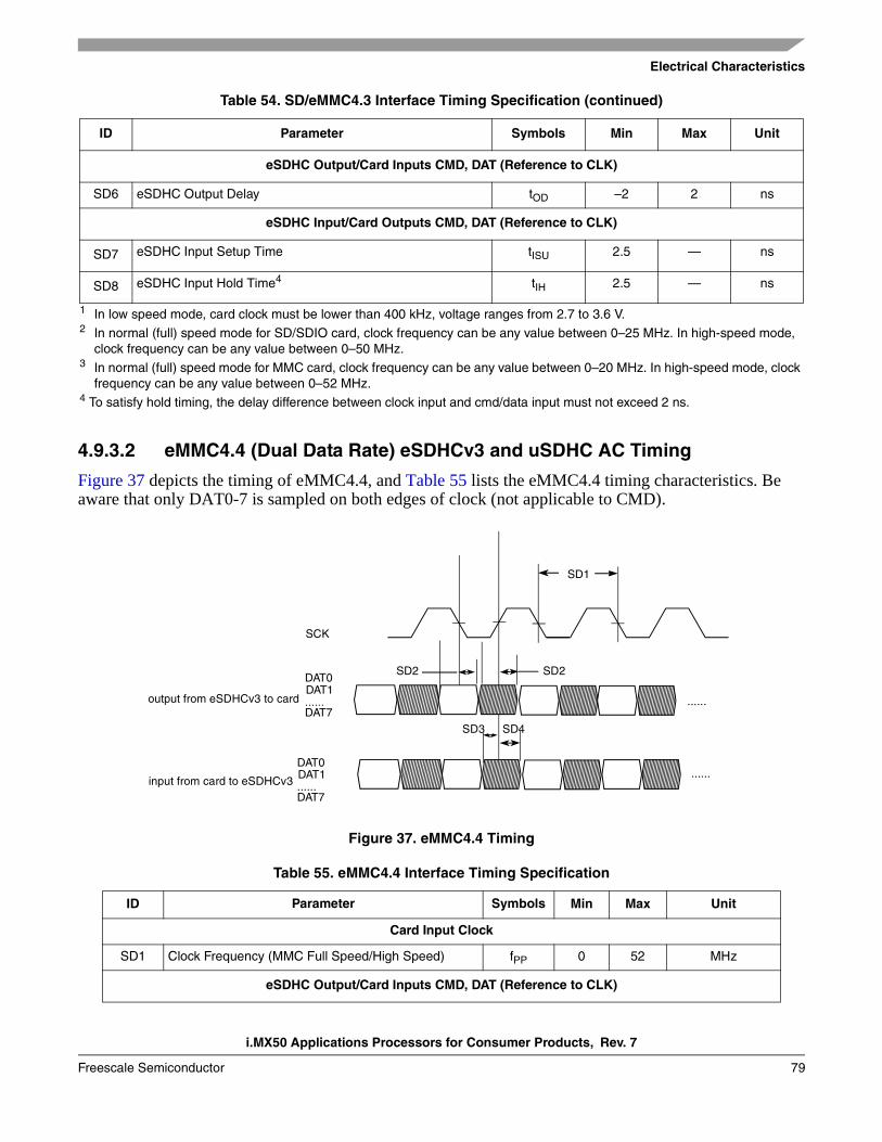
Electrical Characteristics
i.MX50 Applications Processors for Consumer Products, Rev. 7
Freescale Semiconductor 79
4.9.3.2 eMMC4.4 (Dual Data Rate) eSDHCv3 and uSDHC AC Timing
Figure 37 depicts the timing of eMMC4.4, and Table 55 lists the eMMC4.4 timing characteristics. Be aware that only DAT0-7 is sampled on both edges of clock (not applicable to CMD).
Figure 37. eMMC4.4 Timing
eSDHC Output/Card Inputs CMD, DAT (Reference to CLK)
SD6 eSDHC Output Delay tOD –2 2 ns
eSDHC Input/Card Outputs CMD, DAT (Reference to CLK)
SD7 eSDHC Input Setup Time tISU 2.5 — ns
SD8 eSDHC Input Hold Time4 tIH 2.5 — ns
1 In low speed mode, card clock must be lower than 400 kHz, voltage ranges from 2.7 to 3.6 V.2 In normal (full) speed mode for SD/SDIO card, clock frequency can be any value between 0–25 MHz. In high-speed mode,
clock frequency can be any value between 0–50 MHz.3 In normal (full) speed mode for MMC card, clock frequency can be any value between 0–20 MHz. In high-speed mode, clock
frequency can be any value between 0–52 MHz.4 To satisfy hold timing, the delay difference between clock input and cmd/data input must not exceed 2 ns.
Table 55. eMMC4.4 Interface Timing Specification
ID Parameter Symbols Min Max Unit
Card Input Clock
SD1 Clock Frequency (MMC Full Speed/High Speed) fPP 0 52 MHz
eSDHC Output/Card Inputs CMD, DAT (Reference to CLK)
Table 54. SD/eMMC4.3 Interface Timing Specification (continued)
ID Parameter Symbols Min Max Unit
SD1
SD2
SD3
output from eSDHCv3 to cardDAT1......DAT7
DAT0
input from card to eSDHCv3 DAT1......DAT7
DAT0
SCK
SD4
SD2
......
......

i.MX50 Applications Processors for Consumer Products, Rev. 7
Electrical Characteristics
Freescale Semiconductor80
4.9.4 FEC AC Timing Parameters
This section describes the AC timing specifications of the FEC. The i.MX50 FEC supports 10/100 Mbps RMII with MII serial management interface. The RMII and serial management signals are compatible with transceivers operating at a voltage of 3.3 V.
4.9.4.1 RMII Async Inputs Signal Timing (FEC_COL)
Table 56 lists RMII asynchronous inputs signal timing information. Figure 38 shows MII asynchronous input timings listed in Table 56.
.
Figure 38. MII Async Inputs Timing Diagram
4.9.4.2 RMII Serial Management Channel Timing (FEC_MDIO and FEC_MDC)
Table 57 lists RMII serial management channel timings. Figure 39 shows RMII serial management channel timings listed in Table 57. The MDC frequency should be equal to or less than 2.5 MHz to be compliant with the IEEE 802.3 RMII specification. However, the FEC can function correctly with a maximum MDC frequency of 15 MHz.
SD2 eSDHC Output Delay tOD –5 5 ns
eSDHC Input/Card Outputs CMD, DAT (Reference to CLK)
SD3 eSDHC Input Setup Time tISU 2.5 — ns
SD4 eSDHC Input Hold Time tIH 1.5 — ns
Table 56. RMII Async Inputs Signal Timing
Num Characteristics Min Max Unit
M9 FEC_COL minimum pulse width 1.5 — FEC_TX_CLK period
Table 57. RMII Transmit Signal Timing
ID Characteristics Min Max Unit
M10 FEC_MDC falling edge to FEC_MDIO output invalid (minimum propagation delay) 0 — ns
M11 FEC_MDC falling edge to FEC_MDIO output valid (max propagation delay) — 5 ns
M12 FEC_MDIO (input) to FEC_MDC rising edge setup 18 — ns
M13 FEC_MDIO (input) to FEC_MDC rising edge hold 0 — ns
Table 55. eMMC4.4 Interface Timing Specification (continued)
ID Parameter Symbols Min Max Unit
FEC_COL
M9

Electrical Characteristics
i.MX50 Applications Processors for Consumer Products, Rev. 7
Freescale Semiconductor 81
Figure 39. RMII Serial Management Channel Timing Diagram
4.9.4.3 RMII Mode Timing
In RMII mode, FEC_TX_CLK is used as the REF_CLK which is a 50 MHz ± 50 ppm continuous reference clock. FEC_RX_DV is used as the CRS_DV in RMII, and other signals under RMII mode include FEC_TX_EN, FEC_TXD[1:0], FEC_RXD[1:0] and optional FEC_RX_ER.
The RMII mode timings are shown in Table 58 and Figure 40.
M14 FEC_MDC pulse width high 40% 60% FEC_MDC period
M15 FEC_MDC pulse width low 40% 60% FEC_MDC period
Table 58. RMII Signal Timing
No. Characteristics Min Max Unit
M16 REF_CLK(FEC_TX_CLK) pulse width high 35% 65% REF_CLK period
M17 REF_CLK(FEC_TX_CLK) pulse width low 35% 65% REF_CLK period
M18 REF_CLK to FEC_TXD[1:0], FEC_TX_EN invalid 2 — ns
M19 REF_CLK to FEC_TXD[1:0], FEC_TX_EN valid — 16 ns
M20 FEC_RXD[1:0], CRS_DV(FEC_RX_DV), FEC_RX_ER to REF_CLK setup
4 — ns
M21 REF_CLK to FEC_RXD[1:0], FEC_RX_DV, FEC_RX_ER hold 2 — ns
Table 57. RMII Transmit Signal Timing (continued)
ID Characteristics Min Max Unit
FEC_MDC (output)
FEC_MDIO (output)
M14
M15
M10
M11
M12 M13
FEC_MDIO (input)

i.MX50 Applications Processors for Consumer Products, Rev. 7
Electrical Characteristics
Freescale Semiconductor82
Figure 40. RMII Mode Signal Timing Diagram
4.9.5 I2C Module Timing ParametersThis section describes the timing parameters of the I2C module. Figure 41 depicts the timing of I2C module, and Table 59 lists the I2C module timing characteristics.
Figure 41. I2C Bus Timing
Table 59. I2C Module Timing Parameters
ID Parameter
Standard ModeSupply Voltage =
1.65 V–1.95 V, 2.7 V–3.3 V
Fast ModeSupply Voltage =
2.7 V–3.3 V Unit
Min Max Min Max
IC1 I2CLK cycle time 10 — 2.5 — µs
IC2 Hold time (repeated) START condition 4.0 — 0.6 — µs
IC3 Set-up time for STOP condition 4.0 — 0.6 — µs
REF_CLK (input)
FEC_TX_EN
M16
M17
M18
M19
M20 M21
FEC_RXD[1:0]
FEC_TXD[1:0] (output)
FEC_RX_ER
CRS_DV (input)
IC10 IC11 IC9
IC2 IC8 IC4 IC7 IC3
IC6
IC10
IC5
IC11 START STOP STARTSTART
I2DAT
I2CLK
IC1

Electrical Characteristics
i.MX50 Applications Processors for Consumer Products, Rev. 7
Freescale Semiconductor 83
4.9.6 One-Wire (OWIRE) Timing Parameters
Figure 42 depicts the RPP timing, and Table 60 lists the RPP timing parameters.
Figure 42. Reset and Presence Pulses (RPP) Timing Diagram
IC4 Data hold time 01 3.452 01 0.92 µs
IC5 HIGH Period of I2CLK Clock 4.0 — 0.6 — µs
IC6 LOW Period of the I2CLK Clock 4.7 — 1.3 — µs
IC7 Set-up time for a repeated START condition 4.7 — 0.6 — µs
IC8 Data set-up time 250 — 1003 — ns
IC9 Bus free time between a STOP and START condition 4.7 — 1.3 — µs
IC10 Rise time of both I2DAT and I2CLK signals — 1000 20 + 0.1Cb4 300 ns
IC11 Fall time of both I2DAT and I2CLK signals — 300 20 + 0.1Cb4 300 ns
IC12 Capacitive load for each bus line (Cb) — 400 — 400 pF
1 A device must internally provide a hold time of at least 300 ns for I2DAT signal in order to bridge the undefined region of the falling edge of I2CLK.
2 The maximum hold time has only to be met if the device does not stretch the LOW period (ID no IC5) of the I2CLK signal.3 A Fast-mode I2C-bus device can be used in a Standard-mode I2C-bus system, but the requirement of Set-up time (ID No IC7)
of 250 ns must be met. This automatically is the case if the device does not stretch the LOW period of the I2CLK signal. If such a device does stretch the LOW period of the I2CLK signal, it must output the next data bit to the I2DAT line max_rise_time (IC9) + data_setup_time (IC7) = 1000 + 250 = 1250 ns (according to the Standard-mode I2C-bus specification) before the I2CLK line is released.
4 Cb = total capacitance of one bus line in pF.
Table 59. I2C Module Timing Parameters (continued)
ID Parameter
Standard ModeSupply Voltage =
1.65 V–1.95 V, 2.7 V–3.3 V
Fast ModeSupply Voltage =
2.7 V–3.3 V Unit
Min Max Min Max
One-Wire bus
One Wire Device Tx “Presence Pulse”
(BATT_LINE)
One-WIRE Tx“Reset Pulse”
OW1
OW2
OW3
OW4tR

i.MX50 Applications Processors for Consumer Products, Rev. 7
Electrical Characteristics
Freescale Semiconductor84
Figure 43 depicts Write 0 Sequence timing, and Table 61 lists the timing parameters.
Figure 43. Write 0 Sequence Timing Diagram
Figure 44 depicts Write 1 Sequence timing, Figure 45 depicts the Read Sequence timing, and Table 62 lists the timing parameters.
Figure 44. Write 1 Sequence Timing Diagram
Table 60. RPP Sequence Delay Comparisons Timing Parameters
ID Parameters Symbol Min Typ Max Unit
OW1 Reset Time Low tRSTL 480 511 —1
1 In order not to mask signaling by other devices on the 1-Wire bus, tRSTL + tR should always be less than 960 µs.
µs
OW2 Presence Detect High tPDH 15 — 60 µs
OW3 Presence Detect Low tPDL 60 — 240 µs
OW4 Reset Time High(includes recovery time)
tRSTH 480 512 — µs
Table 61. WR0 Sequence Timing Parameters
ID Parameter Symbol Min Typ Max Unit
OW5 Write 0 Low Time tLOW0 60 100 120 µs
OW6 Transmission Time Slot tSLOT OW5 117 120 µs
— Recovery time tREC 1 — — µs
OW5
OW6
One-Wire bus (BATT_LINE)
tREC
OW7
OW8
One-Wire bus (BATT_LINE)

Electrical Characteristics
i.MX50 Applications Processors for Consumer Products, Rev. 7
Freescale Semiconductor 85
Figure 45. Read Sequence Timing Diagram
4.9.7 Pulse Width Modulator (PWM) Timing Parameters
This section describes the electrical information of the PWM. The PWM can be programmed to select one of three clock signals as its source frequency. The selected clock signal is passed through a prescaler before being input to the counter. The output is available at the pulse-width modulator output (PWMO) external pin.
Figure 46 depicts the timing of the PWM, and Table 63 lists the PWM timing parameters.
Figure 46. PWM Timing
Table 62. WR1 /RD Timing Parameters
ID Parameter Symbol Min Typ Max Unit
OW7 Write 1 Low Time tLOW1 1 5 15 µs
OW8 Transmission Time Slot tSLOT 60 117 120 µs
— Read Data Setup tSU — — 1 µs
OW9 Read Low Time tLOWR 1 5 15 µs
OW10 Read Data Valid tRDV — 15 — µs
OW11 Release Time tRELEASE 0 — 45 µs
tSU
OW8
OW10
One-Wire bus (BATT_LINE)
OW9OW11
System Clock
2a1
PWM Output
3b
2b3a
4b
4a

i.MX50 Applications Processors for Consumer Products, Rev. 7
Electrical Characteristics
Freescale Semiconductor86
4.9.8 Secure JTAG Controller (SJC) Timing ParametersFigure 47 depicts the SJC test clock input timing. Figure 48 depicts the SJC boundary scan timing. Figure 49 depicts the SJC test access port. Figure 50 depicts the TRST timing. The signal parameters are listed in Table 64.
Figure 47. Test Clock Input Timing Diagram
Table 63. PWM Output Timing Parameter
Ref. No. Parameter Min Max Unit
1 System CLK frequency1
1 CL of PWMO = 30 pF
0 ipg_clk MHz
2a Clock high time 12.29 — ns
2b Clock low time 9.91 — ns
3a Clock fall time — 0.5 ns
3b Clock rise time — 0.5 ns
4a Output delay time — 9.37 ns
4b Output setup time 8.71 — ns
TCK(Input) VM VMVIH
VIL
SJ1
SJ2 SJ2
SJ3SJ3

Electrical Characteristics
i.MX50 Applications Processors for Consumer Products, Rev. 7
Freescale Semiconductor 87
Figure 48. Boundary Scan (JTAG) Timing Diagram
Figure 49. Test Access Port Timing Diagram
TCK(Input)
DataInputs
DataOutputs
DataOutputs
DataOutputs
VIHVIL
Input Data Valid
Output Data Valid
Output Data Valid
SJ4 SJ5
SJ6
SJ7
SJ6
TCK(Input)
TDI
(Input)
TDO(Output)
TDO(Output)
TDO(Output)
VIHVIL
Input Data Valid
Output Data Valid
Output Data Valid
TMS
SJ8 SJ9
SJ10
SJ11
SJ10

i.MX50 Applications Processors for Consumer Products, Rev. 7
Electrical Characteristics
Freescale Semiconductor88
Figure 50. TRST Timing Diagram
Table 64. JTAG Timing
ID Parameter1,2All Frequencies
Unit Min Max
SJ0 TCK frequency of operation 1/(3•TDC)1
1 TDC = target frequency of SJC
0.001 22 MHz
SJ1 TCK cycle time in crystal mode 45 — ns
SJ2 TCK clock pulse width measured at VM2
2 VM = mid-point voltage
22.5 — ns
SJ3 TCK rise and fall times — 3 ns
SJ4 Boundary scan input data set-up time 5 — ns
SJ5 Boundary scan input data hold time 24 — ns
SJ6 TCK low to output data valid — 40 ns
SJ7 TCK low to output high impedance — 40 ns
SJ8 TMS, TDI data set-up time 5 — ns
SJ9 TMS, TDI data hold time 25 — ns
SJ10 TCK low to TDO data valid — 44 ns
SJ11 TCK low to TDO high impedance — 44 ns
SJ12 TRST assert time 100 — ns
SJ13 TRST set-up time to TCK low 40 — ns
TCK(Input)
TRST(Input)
SJ13
SJ12
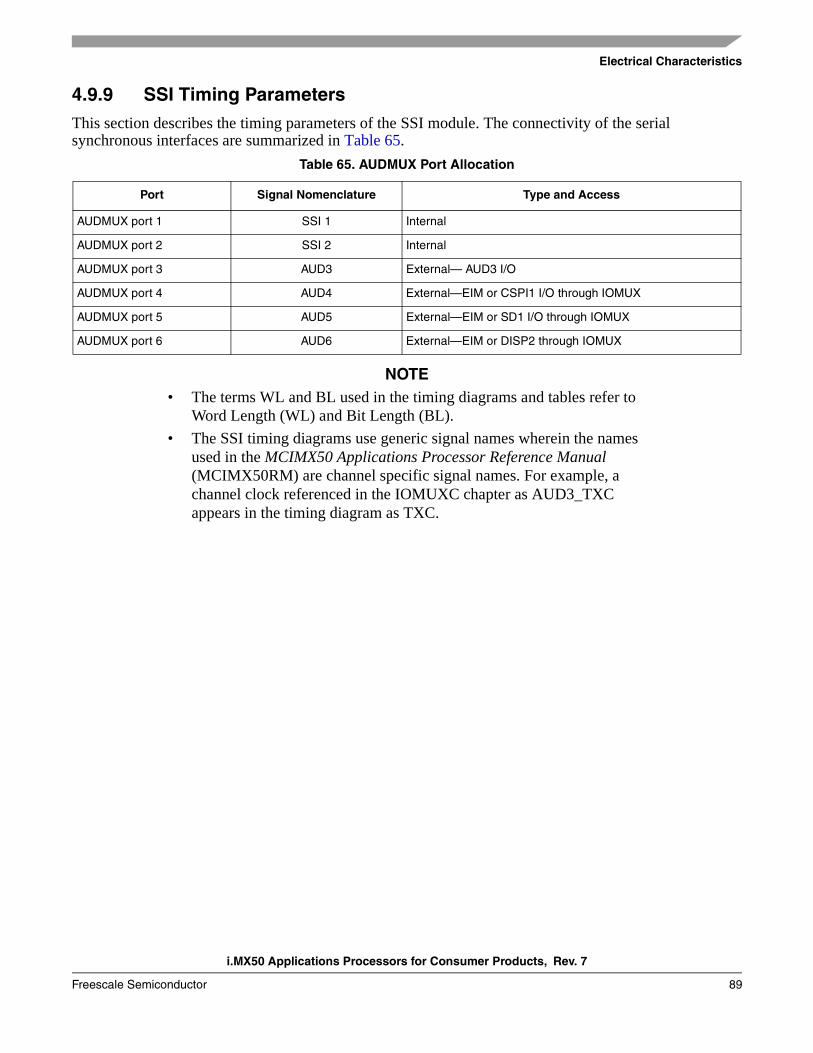
Electrical Characteristics
i.MX50 Applications Processors for Consumer Products, Rev. 7
Freescale Semiconductor 89
4.9.9 SSI Timing ParametersThis section describes the timing parameters of the SSI module. The connectivity of the serial synchronous interfaces are summarized in Table 65.
NOTE• The terms WL and BL used in the timing diagrams and tables refer to
Word Length (WL) and Bit Length (BL).
• The SSI timing diagrams use generic signal names wherein the names used in the MCIMX50 Applications Processor Reference Manual (MCIMX50RM) are channel specific signal names. For example, a channel clock referenced in the IOMUXC chapter as AUD3_TXC appears in the timing diagram as TXC.
Table 65. AUDMUX Port Allocation
Port Signal Nomenclature Type and Access
AUDMUX port 1 SSI 1 Internal
AUDMUX port 2 SSI 2 Internal
AUDMUX port 3 AUD3 External— AUD3 I/O
AUDMUX port 4 AUD4 External—EIM or CSPI1 I/O through IOMUX
AUDMUX port 5 AUD5 External—EIM or SD1 I/O through IOMUX
AUDMUX port 6 AUD6 External—EIM or DISP2 through IOMUX

i.MX50 Applications Processors for Consumer Products, Rev. 7
Electrical Characteristics
Freescale Semiconductor90
4.9.9.1 SSI Transmitter Timing with Internal Clock
Figure 51 depicts the SSI transmitter internal clock timing and Table 66 lists the timing parameters for the SSI transmitter internal clock.
.
Figure 51. SSI Transmitter Internal Clock Timing Diagram
Table 66. SSI Transmitter Timing with Internal Clock
ID Parameter Min Max Unit
Internal Clock Operation
SS1 (Tx/Rx) CK clock period 81.4 — ns
SS2 (Tx/Rx) CK clock high period 36.0 — ns
SS3 (Tx/Rx) CK clock rise time — 6.0 ns
SS4 (Tx/Rx) CK clock low period 36.0 — ns
SS5 (Tx/Rx) CK clock fall time — 6.0 ns
SS6 (Tx) CK high to FS (bl) high — 15.0 ns
SS8 (Tx) CK high to FS (bl) low — 15.0 ns
SS10 (Tx) CK high to FS (wl) high — 15.0 ns
SS12 (Tx) CK high to FS (wl) low — 15.0 ns
SS14 (Tx/Rx) Internal FS rise time — 6.0 ns
SS15 (Tx/Rx) Internal FS fall time — 6.0 ns
SS16 (Tx) CK high to STXD valid from high impedance — 15.0 ns
SS19
SS1
SS2 SS4
SS3SS5
SS6 SS8
SS10 SS12
SS14
SS18SS15
SS17SS16
SS43SS42
Note: SRXD input in synchronous mode only
TXC(Output)
TXFS (wl)(Output)
TXFS (bl)(Output)
RXD(Input)
TXD(Output)

Electrical Characteristics
i.MX50 Applications Processors for Consumer Products, Rev. 7
Freescale Semiconductor 91
NOTE• All the timings for the SSI are given for a non-inverted serial clock
polarity (TSCKP/RSCKP = 0) and a non-inverted frame sync (TFSI/RFSI = 0). If the polarity of the clock and/or the frame sync have been inverted, all the timing remains valid by inverting the clock signal STCK/SRCK and/or the frame sync STFS/SRFS shown in both the tables and figures.
• All timings are on Audiomux Pads when SSI is being used for data transfer.
• The terms WL and BL refer to word length (WL) and bit length (BL).
• Tx and Rx refer to the transmit and receive sections of the SSI.
• For internal frame sync operation using external clock, the FS timing is same as that of Tx Data (for example, during AC97 mode of operation).
SS17 (Tx) CK high to STXD high/low — 15.0 ns
SS18 (Tx) CK high to STXD high impedance — 15.0 ns
SS19 STXD rise/fall time — 6.0 ns
Synchronous Internal Clock Operation
SS42 SRXD setup before (Tx) CK falling 10.0 — ns
SS43 SRXD hold after (Tx) CK falling 0.0 — ns
SS52 Loading — 25.0 pF
Table 66. SSI Transmitter Timing with Internal Clock (continued)
ID Parameter Min Max Unit

i.MX50 Applications Processors for Consumer Products, Rev. 7
Electrical Characteristics
Freescale Semiconductor92
4.9.9.2 SSI Receiver Timing with Internal Clock
Figure 52 depicts the SSI receiver internal clock timing and Table 67 lists the timing parameters for the receiver timing with internal clock.
Figure 52. SSI Receiver Internal Clock Timing Diagram
Table 67. SSI Receiver Timing with Internal Clock
ID Parameter Min Max Unit
Internal Clock Operation
SS1 (Tx/Rx) CK clock period 81.4 — ns
SS2 (Tx/Rx) CK clock high period 36.0 — ns
SS3 (Tx/Rx) CK clock rise time — 6.0 ns
SS4 (Tx/Rx) CK clock low period 36.0 — ns
SS5 (Tx/Rx) CK clock fall time — 6.0 ns
SS7 (Rx) CK high to FS (bl) high — 15.0 ns
SS9 (Rx) CK high to FS (bl) low — 15.0 ns
SS11 (Rx) CK high to FS (wl) high — 15.0 ns
SS13 (Rx) CK high to FS (wl) low — 15.0 ns
SS20 SRXD setup time before (Rx) CK low 10.0 — ns
SS21 SRXD hold time after (Rx) CK low 0.0 — ns
SS50SS48
SS1
SS4SS2
SS51
SS20SS21
SS49
SS7 SS9
SS11 SS13
SS47
SS3SS5
TXC(Output)
TXFS (bl)(Output)
TXFS (wl)(Output)
RXD(Input)
RXC(Output)

Electrical Characteristics
i.MX50 Applications Processors for Consumer Products, Rev. 7
Freescale Semiconductor 93
NOTE• All the timings for the SSI are given for a non-inverted serial clock
polarity (TSCKP/RSCKP = 0) and a non-inverted frame sync (TFSI/RFSI = 0). If the polarity of the clock and/or the frame sync have been inverted, all the timing remains valid by inverting the clock signal STCK/SRCK and/or the frame sync STFS/SRFS as shown in both the tables and figures.
• All timings are on Audiomux Pads when SSI is being used for data transfer.
• Tx and Rx refer to the transmit and receive sections of the SSI.
• The terms WL and BL refer to word length (WL) and bit length (BL).
• For internal frame sync operation using external clock, the FS timing is same as that of Tx Data (for example, during AC97 mode of operation).
Oversampling Clock Operation
SS47 Oversampling clock period 15.04 — ns
SS48 Oversampling clock high period 6.0 — ns
SS49 Oversampling clock rise time — 3.0 ns
SS50 Oversampling clock low period 6.0 — ns
SS51 Oversampling clock fall time — 3.0 ns
Table 67. SSI Receiver Timing with Internal Clock (continued)
ID Parameter Min Max Unit

i.MX50 Applications Processors for Consumer Products, Rev. 7
Electrical Characteristics
Freescale Semiconductor94
4.9.9.3 SSI Transmitter Timing with External Clock
Figure 53 depicts the SSI transmitter external clock timing and Table 68 lists the timing parameters for the transmitter timing with external clock.
Figure 53. SSI Transmitter External Clock Timing Diagram
Table 68. SSI Transmitter Timing with External Clock
ID Parameter Min Max Unit
External Clock Operation
SS22 (Tx/Rx) CK clock period 81.4 — ns
SS23 (Tx/Rx) CK clock high period 36.0 — ns
SS24 (Tx/Rx) CK clock rise time — 6.0 ns
SS25 (Tx/Rx) CK clock low period 36.0 — ns
SS26 (Tx/Rx) CK clock fall time — 6.0 ns
SS27 (Tx) CK high to FS (bl) high –10.0 15.0 ns
SS29 (Tx) CK high to FS (bl) low 10.0 — ns
SS31 (Tx) CK high to FS (wl) high –10.0 15.0 ns
SS33 (Tx) CK high to FS (wl) low 10.0 — ns
SS37 (Tx) CK high to STXD valid from high impedance — 15.0 ns
SS38 (Tx) CK high to STXD high/low — 15.0 ns
SS45
SS33
SS24SS26
SS25SS23
Note: SRXD Input in Synchronous mode only
SS31
SS29SS27
SS22
SS44
SS39SS38SS37
SS46
TXC(Input)
TXFS (bl)(Input)
TXFS (wl)(Input)
TXD(Output)
RXD(Input)

Electrical Characteristics
i.MX50 Applications Processors for Consumer Products, Rev. 7
Freescale Semiconductor 95
NOTE• All the timings for the SSI are given for a non-inverted serial clock
polarity (TSCKP/RSCKP = 0) and a non-inverted frame sync (TFSI/RFSI = 0). If the polarity of the clock and/or the frame sync have been inverted, all the timing remains valid by inverting the clock signal STCK/SRCK and/or the frame sync STFS/SRFS shown in both the tables and figures.
• All timings are on Audiomux Pads when SSI is being used for data transfer.
• Tx and Rx refer to the transmit and receive sections of the SSI.
• The terms WL and BL refer to word length (WL) and bit length (BL).
• For internal frame sync operation using external clock, the FS timing is same as that of Tx Data (for example, during AC97 mode of operation).
SS39 (Tx) CK high to STXD high impedance — 15.0 ns
Synchronous External Clock Operation
SS44 SRXD setup before (Tx) CK falling 10.0 — ns
SS45 SRXD hold after (Tx) CK falling 2.0 — ns
SS46 SRXD rise/fall time — 6.0 ns
Table 68. SSI Transmitter Timing with External Clock (continued)
ID Parameter Min Max Unit

i.MX50 Applications Processors for Consumer Products, Rev. 7
Electrical Characteristics
Freescale Semiconductor96
4.9.9.4 SSI Receiver Timing with External Clock
Figure 54 depicts the SSI receiver external clock timing and Table 69 lists the timing parameters for the receiver timing with external clock.
Figure 54. SSI Receiver External Clock Timing Diagram
Table 69. SSI Receiver Timing with External Clock
ID Parameter Min Max Unit
External Clock Operation
SS22 (Tx/Rx) CK clock period 81.4 — ns
SS23 (Tx/Rx) CK clock high period 36 — ns
SS24 (Tx/Rx) CK clock rise time — 6.0 ns
SS25 (Tx/Rx) CK clock low period 36 — ns
SS26 (Tx/Rx) CK clock fall time — 6.0 ns
SS28 (Rx) CK high to FS (bl) high –10 15.0 ns
SS30 (Rx) CK high to FS (bl) low 10 — ns
SS32 (Rx) CK high to FS (wl) high –10 15.0 ns
SS34 (Rx) CK high to FS (wl) low 10 — ns
SS35 (Tx/Rx) External FS rise time — 6.0 ns
SS36 (Tx/Rx) External FS fall time — 6.0 ns
SS40 SRXD setup time before (Rx) CK low 10 — ns
SS41 SRXD hold time after (Rx) CK low 2 — ns
SS24
SS34
SS35
SS30SS28
SS26
SS25SS23
SS40
SS22
SS32
SS36SS41
TXC(Input)
TXFS (bl)(Input)
TXFS (wl)(Input)
RXD(Input)

Electrical Characteristics
i.MX50 Applications Processors for Consumer Products, Rev. 7
Freescale Semiconductor 97
NOTE• All the timings for the SSI are given for a non-inverted serial clock
polarity (TSCKP/RSCKP = 0) and a non-inverted frame sync (TFSI/RFSI = 0). If the polarity of the clock and/or the frame sync have been inverted, all the timing remains valid by inverting the clock signal STCK/SRCK and/or the frame sync STFS/SRFS shown in both the tables and figures.
• All timings are on Audiomux Pads when SSI is being used for data transfer.
• Tx and Rx refer to the transmit and receive sections of the SSI.
• The terms WL and BL refer to word length (WL) and bit length (BL).
• For internal Frame Sync operation using external clock, the FS timing is same as that of Tx Data (for example, during AC97 mode of operation).
4.9.10 UART I/O Configuration and Timing Parameters
The following sections describe the UART I/O configuration and timing parameters.
4.9.10.1 UART RS-232 I/O Configuration in Different Modes
Table 70 shows the UART I/O configuration based on which mode is enabled.
4.9.10.2 UART RS-232 Serial Mode Timing
The following sections describe the electrical information of the UART module in the RS-232 mode.
Table 70. UART I/O Configuration vs. Mode
PortDTE Mode DCE Mode
Direction Description Direction Description
RTS Output RTS from DTE to DCE Input RTS from DTE to DCE
CTS Input CTS from DCE to DTE Output CTS from DCE to DTE
TXD_MUX Input Serial data from DCE to DTE Output Serial data from DCE to DTE
RXD_MUX Output Serial data from DTE to DCE Input Serial data from DTE to DCE

i.MX50 Applications Processors for Consumer Products, Rev. 7
Electrical Characteristics
Freescale Semiconductor98
4.9.10.2.1 UART Transmitter
Figure 55 depicts the transmit timing of UART in the RS-232 serial mode with 8 data bit/1 stop bit format. Table 71 lists the UART RS-232 serial mode transmit timing characteristics.
Figure 55. UART RS-232 Serial Mode Transmit Timing Diagram
4.9.10.2.2 UART Receiver
Figure 56 depicts the RS-232 serial mode receive timing with 8 data bit/1 stop bit format. Table 72 lists serial mode receive timing characteristics.
Figure 56. UART RS-232 Serial Mode Receive Timing Diagram
4.9.10.3 UART IrDA Mode Timing
The following sections give the UART transmit and receive timings in IrDA mode.
Table 71. RS-232 Serial Mode Transmit Timing Parameters
ID Parameter Symbol Min Max Units
UA1 Transmit Bit Time tTbit 1/Fbaud_rate1 – Tref_clk
2
1 Fbaud_rate: Baud rate frequency. The maximum baud rate the UART can support is (ipg_perclk frequency)/16.2 Tref_clk: The period of UART reference clock ref_clk (ipg_perclk after RFDIV divider).
1/Fbaud_rate + Tref_clk —
Table 72. RS-232 Serial Mode Receive Timing Parameters
ID Parameter Symbol Min Max Units
UA2 Receive Bit Time1
1 The UART receiver can tolerate 1/(16*Fbaud_rate) tolerance in each bit. But accumulation tolerance in one frame must not exceed 3/(16*Fbaud_rate).
tRbit 1/Fbaud_rate2 – 1/(16*Fbaud_rate)
2 Fbaud_rate: Baud rate frequency. The maximum baud rate the UART can support is (ipg_perclk frequency)/16.
1/Fbaud_rate + 1/(16*Fbaud_rate) —
Bit 1 Bit 2Bit 0 Bit 4 Bit 5 Bit 6 Bit 7TXD(output)
Bit 3StartBit STOP
BIT
NextStartBit
PossibleParity
Bit
Par Bit
UA1
UA1 UA1
UA1
Bit 1 Bit 2Bit 0 Bit 4 Bit 5 Bit 6 Bit 7RXD
(input) Bit 3StartBit STOP
BIT
NextStartBit
PossibleParity
Bit
Par Bit
UA2 UA2
UA2 UA2
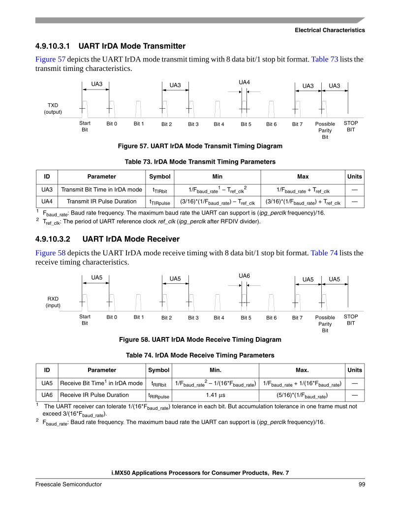
Electrical Characteristics
i.MX50 Applications Processors for Consumer Products, Rev. 7
Freescale Semiconductor 99
4.9.10.3.1 UART IrDA Mode Transmitter
Figure 57 depicts the UART IrDA mode transmit timing with 8 data bit/1 stop bit format. Table 73 lists the transmit timing characteristics.
Figure 57. UART IrDA Mode Transmit Timing Diagram
4.9.10.3.2 UART IrDA Mode Receiver
Figure 58 depicts the UART IrDA mode receive timing with 8 data bit/1 stop bit format. Table 74 lists the receive timing characteristics.
Figure 58. UART IrDA Mode Receive Timing Diagram
Table 73. IrDA Mode Transmit Timing Parameters
ID Parameter Symbol Min Max Units
UA3 Transmit Bit Time in IrDA mode tTIRbit 1/Fbaud_rate1 – Tref_clk
2
1 Fbaud_rate: Baud rate frequency. The maximum baud rate the UART can support is (ipg_perclk frequency)/16.2 Tref_clk: The period of UART reference clock ref_clk (ipg_perclk after RFDIV divider).
1/Fbaud_rate + Tref_clk —
UA4 Transmit IR Pulse Duration tTIRpulse (3/16)*(1/Fbaud_rate) – Tref_clk (3/16)*(1/Fbaud_rate) + Tref_clk —
Table 74. IrDA Mode Receive Timing Parameters
ID Parameter Symbol Min. Max. Units
UA5 Receive Bit Time1 in IrDA mode
1 The UART receiver can tolerate 1/(16*Fbaud_rate) tolerance in each bit. But accumulation tolerance in one frame must not exceed 3/(16*Fbaud_rate).
tRIRbit 1/Fbaud_rate2 – 1/(16*Fbaud_rate)
2 Fbaud_rate: Baud rate frequency. The maximum baud rate the UART can support is (ipg_perclk frequency)/16.
1/Fbaud_rate + 1/(16*Fbaud_rate) —
UA6 Receive IR Pulse Duration tRIRpulse 1.41 μs (5/16)*(1/Fbaud_rate) —
Bit 1 Bit 2Bit 0 Bit 4 Bit 5 Bit 6 Bit 7
TXD(output)
Bit 3StartBit
STOPBIT
PossibleParity
Bit
UA3 UA3 UA3 UA3UA4
Bit 1 Bit 2Bit 0 Bit 4 Bit 5 Bit 6 Bit 7
RXD(input)
Bit 3StartBit
STOPBIT
PossibleParity
Bit
UA5 UA5 UA5 UA5UA6

i.MX50 Applications Processors for Consumer Products, Rev. 7
Electrical Characteristics
Freescale Semiconductor100
4.9.11 USB PHY Parameters
This section describes the USB OTG PHY and the USB host port PHY parameters.
4.9.11.1 USB PHY AC Parameters
Table 75 lists the AC timing parameters for USB PHY.
4.9.11.2 USB PHY Additional Electrical Parameters
Table 76 lists the parameters for additional electrical characteristics for USB PHY.
4.9.11.3 USB PHY System Clocking (SYSCLK)
Table 77 lists the USB PHY system clocking parameters
Table 75. USB PHY AC Timing Parameters
Parameter Conditions Min Typ Max Unit
trise 1.5Mbps12Mbps
480Mbps
754
0.5
— 30020
ns
tfall 1.5Mbps12Mbps
480Mbps
754
0.5
— 30020
ns
Jitter 1.5Mbps12Mbps
480Mbps
— — 101
0.2
ns
Table 76. Additional Electrical Characteristics for USB PHY
Parameter Conditions Min Typ Max Unit
Vcm DC(dc level measured at receiver connector)
HS ModeLS/FS Mode
–0.050.8
— 0.52.5
V
Crossover Voltage LS ModeFS Mode
1.31.3
— 22
V
Power supply ripple noise(analog 3.3 V)
< 160 MHz –50 0 50 mV
Power supply ripple noise(analog 2.5 V)
< 1.2 MHz> 1.2 MHz
–10–50
00
1050
mV
Power supply ripple noise(Digital 1.2 V)
All conditions –50 0 50 mV
Table 77. USB PHY System Clocking Parameters
Parameter Conditions Min Typ Max Unit
Clock deviation Reference Clock frequency 24 MHz
–150 — 150 ppm
Rise/fall time — — — 200 ps

Package Information and Contact Assignments
i.MX50 Applications Processors for Consumer Products, Rev. 7
Freescale Semiconductor 101
4.9.11.4 USB VBUS Parameters
Table 78 lists the USB VBUS input parameters.
5 Package Information and Contact AssignmentsThis section includes the contact assignment information and mechanical package drawing.
5.1 13 x 13 mm, 0.5 mm Pitch, 416 Pin MAPBGA Package InformationThis section contains the outline drawing, signal assignment map, ground, power, reference ID (by ball grid location) for the 13 x 13 mm, 0.5 mm pitch, 416 pin MAPBGA package.
Jitter (peak-peak) <1.2 MHz 0 — 50 ps
Jitter (peak-peak) >1.2 MHz 0 — 100 ps
Duty-cycle Reference Clock frequency 24 MHz
40 — 60 %
Table 78. VBUS Comparators Thresholds
Parameter Conditions Min Typ Max Unit
A-Device Session Valid Comparator Threshold
— 0.8 1.4 2.0 V
B-Device Session Valid Comparator Threshold
— 0.8 1.4 4.0 V
B-Device Session End Comparator Threshold
— 0.2 0.45 0.8 V
VBUS Valid Comparator Threshold1
1 For VBUS maximum rating, see Table 7.
— 4.4 4.6 4.75 V
VBUS for CHGR_DET_B Operation — 3.0 — — V
VBUS Input Current VBUS = 5.25 V — — 350 μA
Table 77. USB PHY System Clocking Parameters (continued)
Parameter Conditions Min Typ Max Unit

i.MX50 Applications Processors for Consumer Products, Rev. 7
Package Information and Contact Assignments
Freescale Semiconductor102
5.1.1 Case 416 MAPBGA, 13 x 13 mm, 0.5 mm Pitch Package ViewsFigure 59 shows the top view of the 13 x 13 mm package, Figure 60 shows the bottom view (416 soldier balls) of the 13 x 13 mm package, and Figure 61 shows the side view of the 13 x 13 mm package.
Figure 59. 416 MAPBGA 13x13 mm Package Top View
Figure 60. 416 MAPBGA 13x13 mm Package Bottom View

Package Information and Contact Assignments
i.MX50 Applications Processors for Consumer Products, Rev. 7
Freescale Semiconductor 103
Figure 61. 416 MAPBGA 13x13 mm Package Side View
The following notes apply to Figure 59, Figure 60, and Figure 61:
• Unless otherwise specified dimensions are in millimeters.
• All dimensions and tolerances conform to ASME Y14.5M-1994.
• Parallelism measurement shall exclude any effect of mark on top surface of package.

i.MX50 Applications Processors for Consumer Products, Rev. 7
Package Information and Contact Assignments
Freescale Semiconductor104
5.1.2 416 MAPBGA 13 x 13 mm, 0.5 mm Pitch Ball MapTable 79 shows the 416 MAPBGA 13 x 13 mm, 0.5 mm pitch ball map.
Table 79. 416 MAPBGA 13x13 mm, 0.5 mm Pitch Ball Map
1 2 3 4 5 6 7 8 9 10 11 12 13 14 15 16 17 18 19 20 21 22 23 24
A
VS
S
EIM
_RD
Y
EIM
_CR
E
EIM
_EB
0
EIM
_BC
LK
EIM
_DA
12
EIM
_DA
8
EIM
_DA
4
EIM
_DA
0
EP
DC
_SD
SH
R
EP
DC
_GD
CLK
EP
DC
_GD
RL
EP
DC
_SD
CLK
EP
DC
_D12
EP
DC
_D8
EP
DC
_D4
EP
DC
_D0
VS
S
DR
AM
_D30
DR
AM
_D29
NV
CC
_EM
I_D
RA
M
DR
AM
_D26
DR
AM
_D25
VS
S
A
B
KE
Y_C
OL0
KE
Y_C
OL1
EIM
_OE
EIM
_EB
1
EIM
_RW
EIM
_DA
13
EIM
_DA
9
EIM
_DA
5
EIM
_DA
1
EIM
_CS
0
EP
DC
_GD
OE
EP
DC
_GD
SP
EP
DC
_SD
CLK
N
EP
DC
_D13
EP
DC
_D9
EP
DC
_D5
EP
DC
_D1
VS
S
DR
AM
_D31
DR
AM
_D28
NV
CC
_EM
I_D
RA
M
DR
AM
_D27
DR
AM
_D24
DR
AM
_DQ
M3
B
C
KE
Y_C
OL2
KE
Y_C
OL3
NC
NC
NC
NC
NC
NC
NC
NC
NC
NC
NC
NC
NC
NC
NC
NC
NC
NC
NC
NC
DR
AM
_SD
QS
3
DR
AM
_SD
QS
3_B
C
D
KE
Y_R
OW
0
KE
Y_R
OW
1
NC
KE
Y_R
OW
2
EIM
_WA
IT
EIM
_DA
14
EIM
_DA
10
EIM
_DA
6
EIM
_DA
2
EIM
_CS
1
EP
DC
_SD
CE
4
EP
DC
_SD
CE
2
EP
DC
_SD
CE
0
EP
DC
_D14
EP
DC
_D10
EP
DC
_D6
EP
DC
_D2
EP
DC
_SD
LE
EP
DC
_SD
OE
D
EP
DC
_VC
OM
1
NV
CC
_EM
I_D
RA
M
NC
NV
CC
_EM
I_D
RA
M
NV
CC
_EM
I_D
RA
M
D
E
I2C
1_S
CL
I2C
1_S
DA
NC
KE
Y_R
OW
3
EIM
_LB
A
EIM
_DA
15
EIM
_DA
11
EIM
_DA
7
EIM
_DA
3
EIM
_CS
2
EP
DC
_SD
CE
5
EP
DC
_SD
CE
3
EP
DC
_SD
CE
1
EP
DC
_D15
EP
DC
_D11
EP
DC
_D7
EP
DC
_D3
EP
DC
_SD
OE
EP
DC
_SD
OE
Z
EP
DC
_BD
R0
EP
DC
_BD
R1
NC
DR
AM
_D15
DR
AM
_D14
E
F
I2C
2_S
CL
I2C
2_S
DA
NC
PW
M2
PW
M1
NC
NC
NC
NC
NC
NC
NC
NC
NC
NC
NC
NC
NC
NC
DR
AM
_A14
DR
AM
_A13
NC
DR
AM
_D12
DR
AM
_D13
F
G
I2C
3_S
CL
I2C
3_S
DA
NC
EP
ITO
WD
OG
NC
OW
IRE
VD
DG
P
VD
DG
P
VD
DG
P
EP
DC
_PW
RC
OM
EP
DC
_PW
RC
TR
L0
EP
DC
_PW
RC
TR
L1
EP
DC
_PW
RC
TR
L2
EP
DC
_PW
RC
TR
L3
EP
DC
_PW
RS
TAT
EP
DC
_VC
OM
0
DR
AM
_SD
OD
T0
NC
VS
S
VS
S
NC
VS
S
DR
AM
_D10
G

Package Information and Contact Assignments
i.MX50 Applications Processors for Consumer Products, Rev. 7
Freescale Semiconductor 105
H
UA
RT
1_T
XD
UA
RT
1_C
TS
NC
SS
I_T
XF
S
SS
I_T
XD
NC
SS
I_R
XF
S
VD
DG
P
VD
DG
P
VD
DG
P
VD
DG
P
VS
S
VS
S
VC
C
VC
C
VC
C
VC
C
DR
AM
_OP
EN
FB
NC
DR
AM
_A12
DR
AM
_RA
S
NC
DR
AM
_D11
DR
AM
_D9
H
J
UA
RT
1_R
XD
UA
RT
1_R
TS
NC
SS
I_T
XC
SS
I_R
XD
NC
SS
I_R
XC
VD
DG
P
NC
NC
NC
NC
NC
NC
NC
NC
VC
C
DR
AM
_OP
EN
NC
DR
AM
_A11
DR
AM
_CA
S
NC
DR
AM
_D8
DR
AM
_DQ
M1
J
K
UA
RT
2_T
XD
UA
RT
2_C
TS
NC
UA
RT
3_T
XD
UA
RT
4_T
XD
NC
VD
DG
P
VD
DG
P
NC
VD
DG
P
VD
DG
P
VS
S
VS
S
VC
C
VC
C
NC
VC
C
DR
AM
_SD
BA
0
NC
DR
AM
_A10
NV
CC
_EM
I_D
RA
M
NC
NV
CC
_EM
I_D
RA
M
NV
CC
_EM
I_D
RA
M
K
L
UA
RT
2_R
XD
UA
RT
2_R
TS
NC
UA
RT
3_R
XD
UA
RT
4_R
XD
NC
NV
CC
_EIM
VD
DG
P
NC
VD
DG
P
VD
DG
P
VS
S
VS
S
VS
S
VC
C
NC
VS
S
DR
AM
_SD
BA
1
NC
DR
AM
_CA
LIB
RAT
ION
DR
AM
_A9
NC
DR
AM
_SD
QS
1
DR
AM
_SD
QS
1_B
L
M
CS
PI_
SC
LK
CS
PI_
MO
SI
NC
CS
PI_
SS
0
CS
PI_
MIS
O
NC
NV
CC
_EIM
NV
CC
_EIM
NC
NV
CC
_EP
DC
VS
S
NC
NC
VS
S
VS
S
NC
VS
S
VS
S
NC
VS
S
VS
S
NC
VR
EF
DR
AM
_SD
CLK
_0_B
M
N
EC
SP
I1_S
CLK
EC
SP
I1_M
OS
I
NC
EC
SP
I2_S
S0
EC
SP
I2_M
ISO
NC
EC
SP
I1_M
ISO
NV
CC
_KE
YPA
D
NC
NV
CC
_EP
DC
VS
S
NC
NC
VS
S
VS
S
NC
VS
S
DR
AM
_SD
BA
2
NC
DR
AM
_A7
DR
AM
_A8
NC
VD
DO
25
DR
AM
_SD
CLK
_0
N
P
SD
1_C
LK
SD
1_D
1
NC
EC
SP
I2_S
CLK
EC
SP
I2_M
OS
I
NC
EC
SP
I1_S
S0
NV
CC
_MIS
C
NC
NV
CC
_EP
DC
VS
S
VS
S
VS
S
VS
S
VD
DA
L1
NC
VD
DA
DR
AM
_SD
WE
NC
DR
AM
_A5
DR
AM
_A6
NC
DR
AM
_SD
QS
0
DR
AM
_SD
QS
0_B
P
Table 79. 416 MAPBGA 13x13 mm, 0.5 mm Pitch Ball Map (continued)

i.MX50 Applications Processors for Consumer Products, Rev. 7
Package Information and Contact Assignments
Freescale Semiconductor106
R
SD
1_C
MD
SD
1_D
0
NC
SD
1_D
2
SD
1_D
3
NC
NV
CC
_SP
I
NV
CC
_SS
I
NC
NV
CC
_EP
DC
VS
S
VS
S
VS
S
VS
S
VD
DA
L1
NC
VD
DA
DR
AM
_SD
OD
T1
NC
DR
AM
_SD
CLK
_1_B
NV
CC
_EM
I_D
RA
M
NC
NV
CC
_EM
I_D
RA
M
NV
CC
_EM
I_D
RA
M
R
T
SD
2_D
0
SD
2_D
1
NC
SD
2_C
D
SD
2_W
P
NC
NV
CC
_SD
1
NV
CC
_UA
RT
NC
NC
NC
NC
NC
NC
NC
NC
VS
S
VS
S
NC
DR
AM
_SD
CLK
_1
DR
AM
_CS
0
NC
DR
AM
_D6
DR
AM
_DQ
M0
T
U
SD
2_C
LK
SD
2_D
5
NC
SD
2_D
6
SD
2_D
7
NC
JTA
G_T
DO
NV
CC
_SD
2
NV
CC
_JTA
G
NV
CC
_EP
DC
NV
CC
_LC
D
VS
S
VS
S
VS
S
VS
S
VS
S
VS
S
VS
S
NC
DR
AM
_SD
CK
E
DR
AM
_CS
1
NC
DR
AM
_D5
DR
AM
_D7
U
V
SD
2_D
2
SD
2_D
3
NC
SD
2_D
4
SD
2_C
MD
NC
JTA
G_M
OD
NV
CC
_RE
SE
T
NV
CC
_NA
ND
F
NV
CC
_NA
ND
F
CH
GR
_DE
T_B
DIS
P_D
11
DIS
P_D
12
DIS
P_D
13
DIS
P_D
14
DIS
P_D
15
VS
S
VS
S
NC
VS
S
VS
S
NC
VS
S
DR
AM
_D4
V
W
PM
IC_O
N_R
EQ
PM
IC_S
TB
Y_R
EQ
NC
JTA
G_T
CK
GN
D_D
CD
C
NC
NC
NC
NC
NC
NC
NC
NC
NC
NC
NC
NC
NC
NC
DR
AM
_A0
DR
AM
_A1
NC
DR
AM
_D2
DR
AM
_D3
W
Y
CK
IL
EC
KIL
NC
JTA
G_T
MS
VD
D_D
CD
CO
VD
D_D
CD
CI
US
B_O
TG
_GPA
NA
IO
US
B_O
TG
_ID
US
B_O
TG
_VB
US
US
B_H
1_V
BU
S
US
B_H
1_G
PAN
AIO
DIS
P_D
1
DIS
P_D
3
DIS
P_D
5
DIS
P_D
7
DIS
P_D
9
DIS
P_D
10
SD
3_D
5
SD
3_D
7
DR
AM
_A2
DR
AM
_A3
NC
DR
AM
_D1
DR
AM
_D0
Y
AA
NV
CC
_SR
TC
NG
ND
_SR
TC
NC
JTA
G_T
DI
JTA
G_T
RS
TB
CK
IH
GN
D_K
EL
US
B_O
TG
_RR
EF
EX
T
VS
S
US
B_H
1_R
RE
FE
XT
VS
S
DIS
P_D
0
DIS
P_D
2
DIS
P_D
4
DIS
P_D
6
DIS
P_D
8
SD
3_D
3
SD
3_D
4
SD
3_D
6
DR
AM
_A4
NV
CC
_EM
I_D
RA
M
NC
NV
CC
_EM
I_D
RA
M
NV
CC
_EM
I_D
RA
M
AA
Table 79. 416 MAPBGA 13x13 mm, 0.5 mm Pitch Ball Map (continued)

Package Information and Contact Assignments
i.MX50 Applications Processors for Consumer Products, Rev. 7
Freescale Semiconductor 107
5.1.3 416 MAPBGA 13 x 13 Power Rails
AB
BO
OT
_MO
DE
0
BO
OT
_MO
DE
1
NC
NC
NC
NC
NC
NC
NC
NC
NC
NC
NC
NC
NC
NC
NC
NC
NC
NC
NC
NC
DR
AM
_SD
QS
2
DR
AM
_SD
QS
2_B
AB
AC
RE
SE
T_I
N_B
TE
ST
_MO
DE
GN
D3P
0
GN
D2P
5
EX
TAL
GN
D1P
2
GN
D1P
8
US
B_O
TG
_DN
US
B_O
TG
_VD
DA
25_1
US
B_H
1_D
N
US
B_H
1_V
DD
A33
DIS
P_B
US
Y
DIS
P_R
S
DIS
P_R
ES
ET
SD
3_D
0
SD
3_D
1
SD
3_D
2
VS
S
DR
AM
_D16
DR
AM
_D18
NV
CC
_EM
I_D
RA
M
DR
AM
_D20
DR
AM
_D22
DR
AM
_DQ
M2
AC
AD
VS
S
PO
R_B
VD
D3P
0
VD
D2P
5
XTA
L
VD
D1P
2
VD
D1P
8
US
B_O
TG
_DP
US
B_H
1_V
DD
A25
_1
US
B_H
1_D
P
US
B_O
TG
_VD
DA
33
DIS
P_W
R
DIS
P_R
D
DIS
P_C
S
SD
3_W
P
SD
3_C
LK
SD
3_C
MD
VS
S
DR
AM
_D17
DR
AM
_D19
NV
CC
_EM
I_D
RA
M
DR
AM
_D21
DR
AM
_D23
VS
S
AD
1 2 3 4 5 6 7 8 9 10 11 12 13 14 15 16 17 18 19 20 21 22 23 24
Table 80. 416 MAPBGA 13x13 Ground, Power, Sense, and Reference Contact Signals
Pin Name Ball Number Comments
GND_DCDC W5 —
NVCC_EIM L7, M7, M8 —
NVCC_EMI_DRAM A21, AA21, AA23, AA24, AC21, AD21, B21, D21, D23, D24, K21, K23, K24, R21, R23, R24
—
NVCC_EPDC M10, N10, P10, R10, U10 —
NVCC_JTAG U9 —
NVCC_KEYPAD N8 —
NVCC_LCD U11 —
NVCC_MISC P8 —
NVCC_NANDF V9, V10 —
NVCC_RESET V8 —
NVCC_SD1 T7 —
NVCC_SD2 U8 —
NVCC_SPI R7 —
Table 79. 416 MAPBGA 13x13 mm, 0.5 mm Pitch Ball Map (continued)

i.MX50 Applications Processors for Consumer Products, Rev. 7
Package Information and Contact Assignments
Freescale Semiconductor108
NVCC_SRTC AA1 —
NVCC_SSI R8 —
NVCC_UART T8 —
USB_H1_VDDA25 AD9 Note that on the 416 MAPBGA package, USB_OTG_VDDA25 and USB_H1_VDDA25 are shorted together on the substrate.
USB_H1_VDDA33 AC11 Note that on the 416 MAPBGA package, USB_OTG_VDDA33 and USB_H1_VDDA33 are shorted together on the substrate.
USB_OTG_VDDA25 AC9 Note that on the 416 MAPBGA package, USB_OTG_VDDA25 and USB_H1_VDDA25 are shorted together on the substrate.
USB_OTG_VDDA33 AD11 Note that on the 416 MAPBGA package, USB_OTG_VDDA33 and USB_H1_VDDA33 are shorted together on the substrate.
VCC H14, H15, H16, H17, J17, K14, K15, K17, L15 —
VDD_DCDCI Y6 —
VDD_DCDCO Y5 —
VDD1P2 AD6 —
VDD1P8 AD7 —
VDD2P5 AD4 —
VDD3P0 AD3 —
VDDA P17, R17 —
VDDAL1 P15, R15 —
VDDGP G10, G8, G9, H10, H11, H8, H9, J8, K10, K11, K7, K8, L10, L11, L8
—
VDDO25 N23 —
VSS A1, A18, A24, AA11, AA2, AA9, AC18, AC3, AC4, AC6, AC7, AD1, AD18, AD24, B18, G20, G21, G23, H12, H13, K12, K13, L12, L13, L14, L17, M11, M14, M15, M17, M18, M20, M21, N11, N14, N15, N17, P11, P12, P13, P14, R11, R12, R13, R14, T17, T18, U12, U13, U14, U15, U16, U17, U18, V17, V18, V20, V21, V23
—
Table 80. 416 MAPBGA 13x13 Ground, Power, Sense, and Reference Contact Signals (continued)

Package Information and Contact Assignments
i.MX50 Applications Processors for Consumer Products, Rev. 7
Freescale Semiconductor 109
5.2 13 x 13 mm, 0.5 mm Pitch, 416 Pin PoPBGA Package InformationThis section contains the outline drawing, signal assignment map, ground, power, reference ID (by ball grid location) for the 13 x 13 mm, 0.5 mm pitch, 416 pin PoPBGA package.
5.2.1 416 PoPBGA 13 x 13 mm Package Views
Figure shows the top view of the 416 PoPBGA 13 x 13 package, Figure 63 shows the side view of the package, and Figure 64 shows the bottom view of the package.
Figure 62. 416 PoPBGA 13 x 13 mm Package Top View

i.MX50 Applications Processors for Consumer Products, Rev. 7
Package Information and Contact Assignments
Freescale Semiconductor110
Figure 63. 416 PoPBGA 13 x 13 Package Side View
Figure 64. 416 PoPBGA 13 x 13 mm Package Bottom View
The following notes apply to Figure , Figure 63, and Figure 64:
• Unless otherwise specified dimensions are in millimeters.
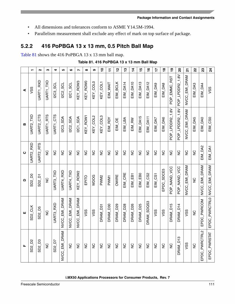
Package Information and Contact Assignments
i.MX50 Applications Processors for Consumer Products, Rev. 7
Freescale Semiconductor 111
• All dimensions and tolerances conform to ASME Y14.5M-1994.
• Parallelism measurement shall exclude any effect of mark on top surface of package.
5.2.2 416 PoPBGA 13 x 13 mm, 0.5 Pitch Ball Map
Table 81 shows the 416 PoPBGA 13 x 13 mm ball map.
Table 81. 416 PoPBGA 13 x 13 mm Ball Map
1 2 3 4 5 6 7 8 9 10 11 12 13 14 15 16 17 18 19 20 21 22 23 24
A
VS
S
UA
RT
1_R
XD
UA
RT
1_T
XD
I2C
3_S
CL
I2C
2_S
CL
I2C
1_S
CL
KE
Y_R
OW
3
KE
Y_R
OW
0
KE
Y_C
OL0
KE
Y_C
OL1
EIM
_WA
IT
EIM
_BC
LK
EIM
_DA
14
EIM
_DA
10
EIM
_DA
13
EIM
_DA
12
EIM
_DA
9
EIM
_DA
8
PO
P_E
MM
C_R
ST
PO
P_L
PD
DR
2_1.
8V
NV
CC
_EM
I_D
RA
M
EIM
_DA
3
EIM
_DA
4
VS
S
B
UA
RT
2_T
XD
UA
RT
2_C
TS
UA
RT
1_R
TS
UA
RT
1_C
TS
I2C
3_S
DA
I2C
2_S
DA
I2C
1_S
DA
KE
Y_R
OW
1
KE
Y_C
OL2
KE
Y_C
OL3
EIM
_RD
Y
EIM
_OE
EIM
_LB
A
EIM
_RW
EIM
_DA
15
EIM
_DA
11
EIM
_DA
7
EIM
_DA
6
PO
P_L
PD
DR
2_1.
8V
PO
P_L
PD
DR
2_1.
8V
NV
CC
_EM
I_D
RA
M
EIM
_DA
5
EIM
_DA
0
EIM
_CS
0
C
UA
RT
2_R
XD
UA
RT
2_R
TS
NC
NC
NC
NC
NC
NC
NC
NC
NC
NC
NC
NC
NC
NC
NC
NC
NC
NC
NC
NC
EIM
_DA
2
EIM
_DA
1
D
SD
2_D
0
SD
2_D
1
NC
UA
RT
3_T
XD
UA
RT
4_R
XD
UA
RT
4_T
XD
KE
Y_R
OW
2
EP
ITO
WD
OG
PW
M2
PW
M1
OW
IRE
EIM
_CR
E
EIM
_EB
1
EIM
_EB
0
EIM
_CS
2
EIM
_CS
1
EP
DC
_SD
CE
5
PO
P_N
AN
D_V
CC
PO
P_N
AN
D_V
CC
NV
CC
_EM
I_D
RA
M
NC
NV
CC
_EM
I_D
RA
M
NV
CC
_EM
I_D
RA
M
E
SD
2_C
LK
SD
2_D
5
NC
UA
RT
3_R
XD
NV
CC
_EM
I_D
RA
M
NV
CC
_EM
I_D
RA
M
NV
CC
_EM
I_D
RA
M
VS
S
VS
S
DR
AM
_D31
DR
AM
_D30
DR
AM
_D29
DR
AM
_D28
DR
AM
_D26
DR
AM
_D25
DR
AM
_SD
QS
3
VS
S
VS
S
DR
AM
_D15
DR
AM
_D14
VS
S
NC
EP
DC
_PW
RC
OM
EP
DC
_PW
RC
TR
L0
F
SD
2_D
2
SD
2_D
3
NC
SD
2_D
7
NV
CC
_EM
I_D
RA
M
NC
NC
NC
NC
NC
NC
NC
NC
NC
NC
NC
NC
NC
NC
DR
AM
_D13
VS
S
NC
EP
DC
_PW
RC
TR
L2
EP
DC
_PW
RS
TAT

i.MX50 Applications Processors for Consumer Products, Rev. 7
Package Information and Contact Assignments
Freescale Semiconductor112
G
SD
2_C
MD
SD
2_D
4
NC
SD
2_W
P
NV
CC
_EM
I_D
RA
M
NC
NV
CC
_EM
I_D
RA
M
VD
DG
P
VD
DG
P
VD
DG
P
VS
S
VS
S
VS
S
DR
AM
_D27
DR
AM
_D24
DR
AM
_SD
QS
3_B
DR
AM
_DQ
M3
DR
AM
_D12
NC
DR
AM
_D10
VS
S
NC
VS
S
EP
DC
_GD
CLK
H
CS
PI_
SC
LK
CS
PI_
MIS
O
NC
SD
2_D
6
DR
AM
_A9
NC
VD
DG
P
VD
DG
P
VD
DG
P
VD
DG
P
VS
S
VS
S
VS
S
VC
C
VC
C
VC
C
VC
C
DR
AM
_D11
NC
DR
AM
_D9
EP
DC
_SD
CE
2
NC
EP
DC
_SD
SH
R
EP
DC
_VC
OM
0
J
CS
PI_
MO
SI
CS
PI_
SS
0
NC
SD
2_C
D
DR
AM
_A8
NC
VD
DG
P
VD
DG
P
NC
NC
NC
NC
NC
NC
NC
NC
VC
C
DR
AM
_D8
NC
DR
AM
_SD
QS
1
EP
DC
_SD
CE
3
NC
EP
DC
_D12
EP
DC
_GD
OE
K
EC
SP
I2_S
S0
EC
SP
I2_M
OS
I
NC
EC
SP
I1_M
ISO
DR
AM
_A7
NC
VD
DG
P
VD
DG
P
NC
VD
DG
P
VS
S
VS
S
VS
S
VC
C
VC
C
NC
VC
C
DR
AM
_SD
QS
1_B
NC
NV
CC
_EM
I_D
RA
M
EP
DC
_SD
CE
4
NC
EP
DC
_PW
RC
TR
L1
EP
DC
_SD
CLK
L
EC
SP
I2_S
CLK
EC
SP
I2_M
ISO
NC
EC
SP
I1_S
S0
DR
AM
_A6
NC
VD
DG
P
VD
DG
P
NC
VD
DG
P
VS
S
VS
S
VS
S
VS
S
VC
C
NC
VS
S
DR
AM
_DQ
M1
NC
NV
CC
_EM
I_D
RA
M
EP
DC
_PW
RC
TR
L3
NC
EP
DC
_GD
RL
EP
DC
_SD
CLK
N
M
SD
1_C
LK
SD
1_D
2
NC
EC
SP
I1_S
CLK
PO
P_L
PD
DR
2_1.
8V
NC
NV
CC
_EIM
NV
CC
_EIM
NC
NV
CC
_EP
DC
VS
S
NC
NC
VS
S
VS
S
NC
VS
S
DR
AM
_DQ
M0
NC
NV
CC
_EM
I_D
RA
M
EP
DC
_D13
NC
VR
EF
EP
DC
_SD
LE
N
SD
1_C
MD
SD
1_D
1
NC
EC
SP
I1_M
OS
I
PO
P_L
PD
DR
2_1.
8V
NC
NV
CC
_EIM
NV
CC
_KE
YPA
D
NC
NV
CC
_EP
DC
VS
S
NC
NC
VS
S
VS
S
NC
VS
S
DR
AM
_SD
QS
0
NC
NV
CC
_EM
I_D
RA
M
EP
DC
_D14
NC
VD
DO
25
EP
DC
_SD
CE
0
Table 81. 416 PoPBGA 13 x 13 mm Ball Map (continued)

Package Information and Contact Assignments
i.MX50 Applications Processors for Consumer Products, Rev. 7
Freescale Semiconductor 113
P
SD
3_D
4
SD
1_D
0
NC
DR
AM
_CA
LIB
RAT
ION
DR
AM
_SD
CLK
_0_B
NC
DR
AM
_A5
NV
CC
_MIS
C
NC
NV
CC
_EP
DC
VS
S
VS
S
VS
S
VS
S
VD
DA
L1
NC
VD
DA
DR
AM
_SD
QS
0_B
NC
NV
CC
_EM
I_D
RA
M
EP
DC
_D15
NC
EP
DC
_GD
SP
EP
DC
_SD
CE
1
R
SD
3_D
2
SD
3_D
6
NC
SD
1_D
3
DR
AM
_SD
CLK
_0
NC
NV
CC
_SP
I
NV
CC
_SS
I
NC
NV
CC
_EP
DC
VS
S
VS
S
VS
S
VS
S
VD
DA
L1
NC
VD
DA
DR
AM
_D7
NC
NV
CC
_EM
I_D
RA
M
EP
DC
_D11
NC
EP
DC
_SD
OE
D
EP
DC
_D4
T
SD
3_C
LK
SD
3_C
MD
NC
SD
3_W
P
DR
AM
_SD
CK
E
NC
NV
CC
_SD
1
NV
CC
_UA
RT
NC
NC
NC
NC
NC
NC
NC
NC
VS
S
DR
AM
_D6
NC
DR
AM
_D4
EP
DC
_D9
NC
EP
DC
_D7
EP
DC
_D5
U
SD
3_D
5
SD
3_D
3
NC
SD
3_D
7
DR
AM
_CS
0
NC
DR
AM
_CS
1
NV
CC
_SD
2
NV
CC
_JTA
G
NV
CC
_EP
DC
NV
CC
_LC
D
VS
S
VS
S
VS
S
VS
S
VS
S
VS
S
DR
AM
_D5
NC
DR
AM
_D3
EP
DC
_SD
OE
Z
NC
EP
DC
_D2
EP
DC
_D6
V
SD
3_D
0
SD
3_D
1
NC
JTA
G_T
DO
JTA
G_M
OD
NC
DR
AM
_A0
NV
CC
_RE
SE
T
NV
CC
_NA
ND
F
NV
CC
_NA
ND
F
DR
AM
_D16
DR
AM
_D18
DR
AM
_D20
DR
AM
_D22
DR
AM
_SD
QS
2_B
DR
AM
_D0
DR
AM
_D2
NV
CC
_EM
I_D
RA
M
NC
NV
CC
_EM
I_D
RA
M
EP
DC
_SD
OE
NC
EP
DC
_D10
EP
DC
_D3
W
PM
IC_O
N_R
EQ
PM
IC_S
TB
Y_R
EQ
NC
JTA
G_T
CK
GN
D_D
CD
C
NC
NC
NC
NC
NC
NC
NC
NC
NC
NC
NC
NC
NC
NC
NV
CC
_EM
I_D
RA
M
EP
DC
_VC
OM
1
NC
EP
DC
_D8
EP
DC
_D1
Y
CK
IL
EC
KIL
NC
JTA
G_T
MS
VD
D_D
CD
CO
VD
D_D
CD
CI
DR
AM
_A1
DR
AM
_A2
DR
AM
_A3
DR
AM
_A4
DR
AM
_D17
DR
AM
_D19
DR
AM
_D21
DR
AM
_D23
DR
AM
_SD
QS
2
DR
AM
_DQ
M2
DR
AM
_D1
NV
CC
_EM
I_D
RA
M
NV
CC
_EM
I_D
RA
M
NV
CC
_EM
I_D
RA
M
EP
DC
_BD
R0
NC
EP
DC
_BD
R1
EP
DC
_D0
Table 81. 416 PoPBGA 13 x 13 mm Ball Map (continued)

i.MX50 Applications Processors for Consumer Products, Rev. 7
Package Information and Contact Assignments
Freescale Semiconductor114
5.2.3 416 PoPBGA 13 x 13 mm Power Rails
Table 82 shows the device connection list for ground, power, sense, and reference contact signals. Table 85 displays an alpha-sorted list of the signal assignments including power rails and associated power supplies.
AA
NV
CC
_SR
TC
VS
S
NC
JTA
G_T
DI
JTA
G_T
RS
TB
CK
IH
GN
D_K
EL
US
B_O
TG
_RR
EF
EX
T
VS
S
US
B_H
1_R
RE
FE
XT
VS
S
US
B_O
TG
_ID
US
B_O
TG
_VB
US
US
B_O
TG
_GPA
NA
IO
CH
GR
_DE
T_B
US
B_H
1_V
BU
S
US
B_H
1_G
PAN
AIO
VS
S
DIS
P_R
ES
ET
DIS
P_R
D
DIS
P_B
US
Y
NC
PO
P_L
PD
DR
2_Z
Q1
PO
P_L
PD
DR
2_Z
Q0
AB
BO
OT
_MO
DE
0
BO
OT
_MO
DE
1
NC
NC
NC
NC
NC
NC
NC
NC
NC
NC
NC
NC
NC
NC
NC
NC
NC
NC
NC
NC
DIS
P_D
14
DIS
P_D
5
AC
RE
SE
T_I
N_B
TE
ST
_MO
DE
VS
S
VS
S
EX
TAL
VS
S
VS
S
US
B_O
TG
_DN
US
B_V
DD
A25
US
B_H
1_D
N
US
B_V
DD
A33
SS
I_T
XF
S
SS
I_T
XC
SS
I_R
XD
DIS
P_D
3
DIS
P_D
1
DIS
P_D
0
VS
S
DIS
P_D
7
DIS
P_D
9
DIS
P_C
S
DIS
P_D
12
DIS
P_D
13
DIS
P_D
4
AD
VS
S
PO
R_B
VD
D3P
0
VD
D2P
5
XTA
L
VD
D1P
2
VD
D1P
8
US
B_O
TG
_DP
US
B_V
DD
A25
US
B_H
1_D
P
US
B_V
DD
A33
SS
I_R
XC
SS
I_R
XF
S
SS
I_T
XD
DIS
P_D
2
DIS
P_D
6
DIS
P_
VS
S
DIS
P_D
11
DIS
P_W
R
DIS
P_D
15
DIS
P_D
10
DIS
P_R
S
VS
S
Table 82. 416 PoPBGA 13 x 13 mm Ground, Power, Sense, and Reference Contact Signals
Pin Name Ball Number Comments
GND_DCDC W5 —
NVCC_EIM N7 M7 M8 —
NVCC_EMI_DRAM A21, B21, D21, D23, D24, E5, E6, E7, F5, G5, G7, K20, L20, M20, N20, P20, R20, V18, V20, W20, Y18, Y19, Y20
These are the 1.2V supply to both the i.MX50 DRAM controller as well as the PoP LPDDR2.
NVCC_EPDC M10, N10, P10, R10, U10 —
NVCC_JTAG U9 —
NVCC_KEYPAD N8 —
NVCC_LCD U11 —
NVCC_MISC P8 —
NVCC_NANDF V9, V10 —
Table 81. 416 PoPBGA 13 x 13 mm Ball Map (continued)

Package Information and Contact Assignments
i.MX50 Applications Processors for Consumer Products, Rev. 7
Freescale Semiconductor 115
NVCC_RESET V8 —
NVCC_SD1 T7 —
NVCC_SD2 U8 —
NVCC_SPI R7 —
NVCC_SRTC AA1 —
NVCC_SSI R8 —
NVCC_UART T8 —
POP_EMMC_RST A19 This is PoP eMMC 4.4 NAND Reset input pin. This pin does not connect to the i.MX50. If using eMMC 4.4 NAND, this pin can be connected to a GPIO. For non 4.4 eMMC applications, leave floating.
POP_LPDDR2_1.8V A20, B19, B20, M5, N5 This is the 1.8V supply for the PoP LPDDR2. These pins do not connect to the i.MX50.
POP_LPDDR2_ZQ0 AA24 This is the PoP LPDDR2 ZQ0 pin. This pin does not connect to the i.MX50. This should be connected on the PCB to a 240 Ω 1% resistor to ground
POP_LPDDR2_ZQ1 AA23 This is the PoP LPDDR2 ZQ1 pin. This pin does not connect to the i.MX50. If used, this should be connected on the PCB to a 240 Ω 1% resistor to ground
POP_NAND_VCC D19, D20 This is the 3.3V I/O and memory supply for the PoP eMMC NAND. Note that because the eMMC memory and I/O domains are shorted together, it is not possible to support 1.8 V I/O for the PoP eMMC NAND.
USB_VDDA25 AC9, AD9 Note that on the PoPBGA package, USB_OTG_VDDA25 and USB_H1_VDDA25 are shorted together.
USB_VDDA33 AC11, AD11 Note that on the PoPBGA package, USB_OTG_VDDA33 and USB_H1_VDDA33 are shorted together.
VCC H14, H15, H16, H17, J17, K14, K15, K17, L15 —
VDD_DCDCI Y6 —
VDD_DCDCO Y5 —
VDD1P2 AD6 —
VDD1P8 AD7 —
Table 82. 416 PoPBGA 13 x 13 mm Ground, Power, Sense, and Reference Contact Signals (continued)

i.MX50 Applications Processors for Consumer Products, Rev. 7
Package Information and Contact Assignments
Freescale Semiconductor116
5.3 17 x 17 mm, 0.8 mm Pitch, 400 Pin MAPBGA Package InformationThis section contains the outline drawing, signal assignment map, ground, power, reference ID (by ball grid location) for the 17 x 17 mm, 0.8 mm pitch, 400 pin MAPBGA package.
VDD2P5 AD4 —
VDD3P0 AD3 —
VDDA P17, R17 —
VDDAL1 P15, R15 —
VDDGP G10, G8, G9, H10, H7, H8, H9, J7, J8, K10, K7, K8, L10, L7, L8
—
VDDO25 N23 —
VSS A1, A24, AA11, AA18, AA2, AA9, AC18, AC3, AC4, AC6, AC7, AD1, AD18, AD24, E17, E18, E21, E8, E9, F21, G11, G12, G13, G21, G23, H11, H12, H13, K11, K12, K13, L11, L12, L13, L14, L17, M11, M14, M15, M17, N11, N14, N15, N17, P11, P12, P13, P14, R11, R12, R13, R14, T17, U12, U13, U14, U15, U16, U17
—
Table 82. 416 PoPBGA 13 x 13 mm Ground, Power, Sense, and Reference Contact Signals (continued)

Package Information and Contact Assignments
i.MX50 Applications Processors for Consumer Products, Rev. 7
Freescale Semiconductor 117
5.3.1 400 MAPBGA 17 x 17 mm Package ViewsFigure 65 shows the top view of the 17 x 17 mm package, Figure 66 shows the bottom view of the package, and Figure 67 shows the side view of the package.
Figure 65. 400 MAPBGA 17x17 mm Package Top view
17A1 INDEX AREA
17
BC
0.15
Top View
4x

i.MX50 Applications Processors for Consumer Products, Rev. 7
Package Information and Contact Assignments
Freescale Semiconductor118
Figure 66. 400 MAPBGA 17x17 mm Package Bottom View

Package Information and Contact Assignments
i.MX50 Applications Processors for Consumer Products, Rev. 7
Freescale Semiconductor 119
Figure 67. 400 MAPBGA 17x17 mm Package Side View
The following notes apply to Figure 65, Figure 66, and Figure 67:
• Unless otherwise specified dimensions are in millimeters.
• All dimensions and tolerances conform to ASME Y14.5M-1994.
• Parallelism measurement shall exclude any effect of mark on top surface of package.
5.3.2 400 MAPBGA 17 x 17 mm Ball Map
Table 83 shows the 400 MAPBGA 17 x 17 mm ball map.
Table 83. 400 MAPBGA 17 x 17 mm Ball Map
1 2 3 4 5 6 7 8 9 10 11 12 13 14 15 16 17 18 19 20
A NC
EIM
_RD
Y
EIM
_CR
E
EIM
_EB
0
EIM
_BC
LK
EIM
_DA
12
EIM
_DA
8
EP
DC
_SD
SH
R
EIM
_DA
4
EP
DC
_GD
RL
EP
DC
_GD
CLK
EP
DC
_SD
CE
1
EP
DC
_D5
EP
DC
_D1
EP
DC
_BD
R0
DR
AM
_D26
DR
AM
_D28
DR
AM
_D29
DR
AM
_D30
NC
B
KE
Y_C
OL0
KE
Y_C
OL1
EIM
_OE
EIM
_EB
1
EIM
_RW
EIM
_DA
13
EIM
_DA
9
EIM
_DA
5
EIM
_DA
1
EIM
_DA
0
EIM
_CS
0
EP
DC
_SD
CE
0
EP
DC
_SD
CLK
EP
DC
_VC
OM
0
EP
DC
_D0
EP
DC
_D2
DR
AM
_D27
DR
AM
_D25
DR
AM
_D24
DR
AM
_D31

i.MX50 Applications Processors for Consumer Products, Rev. 7
Package Information and Contact Assignments
Freescale Semiconductor120
C
KE
Y_C
OL2
KE
Y_C
OL3
KE
Y_R
OW
2
EIM
_WA
IT
EIM
_DA
14
EIM
_DA
10
EIM
_DA
6
EIM
_DA
2
EIM
_CS
1
EP
DC
_GD
OE
EP
DC
_SD
CE
2
EP
DC
_PW
RS
TAT
EP
DC
_SD
OE
EP
DC
_D6
EP
DC
_SD
LE
EP
DC
_D3
DR
AM
_D15
DR
AM
_D14
DR
AM
_SD
QS
3
DR
AM
_SD
QS
3_B
D
KE
Y_R
OW
0
KE
Y_R
OW
1
KE
Y_R
OW
3
EIM
_LB
A
EIM
_DA
15
EIM
_DA
11
EIM
_DA
7
EIM
_DA
3
EIM
_CS
2
EP
DC
_SD
CE
4
EP
DC
_GD
SP
EP
DC
_SD
CLK
N
EP
DC
_D10
EP
DC
_D7
EP
DC
_D4
EP
DC
_BD
R1
DR
AM
_D8
DR
AM
_D12
DR
AM
_D11
DR
AM
_DQ
M3
E
I2C
1_S
CL
I2C
1_S
DA
PW
M2
PW
M1
OW
IRE
EP
DC
_SD
CE
5
EP
DC
_PW
RC
OM
EP
DC
_SD
CE
3
EP
DC
_PW
RC
TR
L1
EP
DC
_PW
RC
TR
L0
EP
DC
_D14
EP
DC
_PW
RC
TR
L2
EP
DC
_D15
EP
DC
_D13
EP
DC
_D8
EP
DC
_D9
DR
AM
_D10
DR
AM
_D13
DR
AM
_A12
DR
AM
_RA
S
F
I2C
2_S
CL
I2C
2_S
DA
SS
I_R
XD
WD
OG
EP
ITO
NV
CC
_EIM
NV
CC
_EIM
NV
CC
_EIM
NV
CC
_EP
DC
NV
CC
_EP
DC
NV
CC
_EP
DC
NV
CC
_EP
DC
EP
DC
_D12
EP
DC
_D11
EP
DC
_PW
RC
TR
L3
EP
DC
_SD
OE
Z
DR
AM
_DQ
M1
DR
AM
_D9
DR
AM
_A13
DR
AM
_CA
LIB
RAT
ION
G
I2C
3_S
CL
I2C
3_S
DA
SS
I_T
XC
SS
I_T
XD
SS
I_R
XF
S
VD
DG
P
VD
DG
P
VD
DG
P
VD
DG
P
VD
DG
P
VS
S
VS
S
VS
S
VS
S
EP
DC
_VC
OM
1
EP
DC
_SD
OE
D
DR
AM
_SD
QS
1
DR
AM
_SD
QS
1_B
DR
AM
_A9
DR
AM
_CA
S
H
UA
RT
1_T
XD
UA
RT
4_T
XD
SS
I_T
XF
S
SS
I_R
XC
NV
CC
_KE
YPA
D
VD
DG
P
VD
DG
P
VD
DG
P
VD
DG
P
VD
DG
P
VS
S
VS
S
VS
S
VS
S
VS
S
NV
CC
_EM
I_D
RA
M
DR
AM
_OP
EN
FB
DR
AM
_OP
EN
DR
AM
_A11
DR
AM
_SD
BA
1
J
UA
RT
1_C
TS
UA
RT
3_T
XD
UA
RT
4_R
XD
CS
PI_
SS
0
NV
CC
_MIS
C
VD
DG
P
VD
DG
P
VS
S
VD
DA
L1
VD
DA
L1
VD
DA
VC
C
VS
S
VS
S
NV
CC
_EM
I_D
RA
M
NV
CC
_EM
I_D
RA
M
DR
AM
_SD
CLK
_0
DR
AM
_SD
CLK
_0_B
DR
AM
_A10
DR
AM
_SD
BA
0
Table 83. 400 MAPBGA 17 x 17 mm Ball Map (continued)

Package Information and Contact Assignments
i.MX50 Applications Processors for Consumer Products, Rev. 7
Freescale Semiconductor 121
K
UA
RT
1_R
XD
UA
RT
1_R
TS
UA
RT
3_R
XD
CS
PI_
MIS
O
NV
CC
_SS
I
VD
DG
P
VD
DG
P
VS
S
VD
DA
VC
C
VC
C
VC
C
VS
S
NV
CC
_EM
I_D
RA
M
NV
CC
_EM
I_D
RA
M
NV
CC
_EM
I_D
RA
M
VR
EF
DR
AM
_SD
OD
T0
DR
AM
_A5
DR
AM
_A7
L
UA
RT
2_T
XD
UA
RT
2_R
XD
CS
PI_
MO
SI
EC
SP
I2_M
ISO
NV
CC
_UA
RT
VD
DG
P
VS
S
VS
S
VS
S
VC
C
VC
C
VC
C
VS
S
VS
S
NV
CC
_EM
I_D
RA
M
NV
CC
_EM
I_D
RA
M
VD
DO
25
DR
AM
_SD
WE
DR
AM
_A6
DR
AM
_A8
M
CS
PI_
SC
LK
EC
SP
I2_S
S0
EC
SP
I1_M
ISO
EC
SP
I1_M
OS
I
NV
CC
_SP
I
VS
S
VS
S
VS
S
VS
S
VC
C
VC
C
VS
S
VS
S
VS
S
VS
S
NV
CC
_EM
I_D
RA
M
DR
AM
_SD
QS
0
DR
AM
_SD
QS
0_B
DR
AM
_SD
BA
2
DR
AM
_D6
N
EC
SP
I2_M
OS
I
EC
SP
I1_S
CLK
EC
SP
I1_S
S0
EC
SP
I2_S
CLK
NV
CC
_SD
1
VS
S
VS
S
VS
S
VS
S
VS
S
VS
S
VS
S
VS
S
NV
CC
_EM
I_D
RA
M
NV
CC
_EM
I_D
RA
M
NV
CC
_EM
I_D
RA
M
DR
AM
_DQ
M0
DR
AM
_D5
DR
AM
_D7
DR
AM
_D4
P
SD
1_D
1
SD
1_D
3
SD
1_D
2
SD
1_C
MD
NV
CC
_SD
2
NV
CC
_RE
SE
T
VS
S
VS
S
NV
CC
_JTA
G
NV
CC
_LC
D
NV
CC
_NA
ND
F
NV
CC
_NA
ND
F
VS
S
VS
S
NV
CC
_EM
I_D
RA
M
NV
CC
_EM
I_D
RA
M
DR
AM
_CS
0
DR
AM
_CS
1
DR
AM
_D3
DR
AM
_D2
R
SD
1_C
LK
SD
1_D
0
SD
2_D
0
SD
2_D
6
NV
CC
_SR
TC
GN
D_D
CD
C
VD
D_D
CD
CI
JTA
G_T
CK
JTA
G_T
MS
VS
S
VS
S
VS
S
VS
S
VS
S
VS
S
NV
CC
_EM
I_D
RA
M
DR
AM
_A4
DR
AM
_SD
CK
E
DR
AM
_D1
DR
AM
_D0
T
SD
2_C
D
SD
2_W
P
SD
2_C
LK
SD
2_D
3
VS
S
VD
D_D
CD
CO
GN
D_K
EL
JTA
G_M
OD
JTA
G_T
DO
CH
GR
_DE
T_B
DIS
P_D
1
DIS
P_C
S
DIS
P_D
13
DIS
P_R
ES
ET
SD
3_D
7
SD
3_D
2
DR
AM
_A0
DR
AM
_A1
DR
AM
_SD
QS
2
DR
AM
_SD
QS
2_B
Table 83. 400 MAPBGA 17 x 17 mm Ball Map (continued)

i.MX50 Applications Processors for Consumer Products, Rev. 7
Package Information and Contact Assignments
Freescale Semiconductor122
U
SD
2_D
1
SD
2_D
5
BO
OT
_MO
DE
1
TE
ST
_MO
DE
VD
D3P
0
VD
D1P
2
JTA
G_T
RS
TB
JTA
G_T
DI
US
B_H
1_R
RE
FE
XT
US
B_H
1_G
PAN
AIO
DIS
P_B
US
Y
DIS
P_D
6
DIS
P_D
5
DIS
P_D
14
SD
3_D
3
SD
3_C
MD
SD
3_D
5
DR
AM
_A2
DR
AM
_D23
DR
AM
_DQ
M2
V
SD
2_C
MD
SD
2_D
4
BO
OT
_MO
DE
0
CK
IH
VD
D2P
5
VD
D1P
8
US
B_O
TG
_GPA
NA
IO
US
B_O
TG
_VB
US
US
B_H
1_V
BU
S
DIS
P_W
R
DIS
P_D
0
DIS
P_R
D
DIS
P_D
7
DIS
P_D
12
DIS
P_D
9
SD
3_D
1
SD
3_D
6
DR
AM
_A3
DR
AM
_D18
DR
AM
_D22
W
SD
2_D
7
SD
2_D
2
RE
SE
T_I
N_B
EC
KIL
VS
S
EX
TAL
US
B_O
TG
_RR
EF
EX
T
US
B_O
TG
_DN
US
B_O
TG
_VD
DA
25
US
B_H
1_D
N
US
B_H
1_V
DD
A33
DIS
P_D
2
DIS
P_D
3
DIS
P_D
11
DIS
P_D
8
SD
3_W
P
SD
3_D
4
DR
AM
_D21
DR
AM
_D19
DR
AM
_D20
Y NC
PM
IC_S
TB
Y_R
EQ
PM
IC_O
N_R
EQ
CK
IL
PO
R_B
XTA
L
US
B_O
TG
_ID
US
B_O
TG
_DP
US
B_H
1_V
DD
A25
US
B_H
1_D
P
US
B_O
TG
_VD
DA
33
DIS
P_R
S
DIS
P_D
4
SD
3_C
LK
DIS
P_D
15
DIS
P_D
10
SD
3_D
0
DR
AM
_D17
DR
AM
_D16
NC
Table 83. 400 MAPBGA 17 x 17 mm Ball Map (continued)

Package Information and Contact Assignments
i.MX50 Applications Processors for Consumer Products, Rev. 7
Freescale Semiconductor 123
5.3.3 400 MAPBGA 17 x 17 Power RailsTable 84. 400 MAPBGA 17x17 Ground, Power, Sense, and Reference Contact Signals
Pin Name Ball Number
NC A1 Y1 A20 Y20
NVCC_EIM F6 F7 F8
NVCC_EMI_DRAM K14 N14 J15 K15 L15 N15 P15 H16 J16 K16 L16 M16 N16 P16 R16
NVCC_EPDC F9 F10 F11 F12
NVCC_JTAG P9
NVCC_KEYPAD H5
NVCC_LCD P10
NVCC_MISC J5
NVCC_NANDF P11 P12
NVCC_RESET P6
NVCC_SD1 N5
NVCC_SD2 P5
NVCC_SPI M5
NVCC_SRTC R5
NVCC_SSI K5
NVCC_UART L5
USB_H1_VDDA25 Y9
USB_H1_VDDA33 W11
USB_OTG_VDDA25 W9
USB_OTG_VDDA33 Y11
VCC K10 L10 M10 K11 L11 M11 J12 K12 L12
VDD1P2 U6
VDD1P8 V6
VDD2P5 V5
VDD3P0 U5
VDDA K9 J11
VDDAL1 J9 J10
VDDGP G6 H6 J6 K6 L6 G7 H7 J7 K7 G8 H8 G9 H9 G10 H10
VDDO25 L17
VSS T5 W5 M6 N6 L7 M7 N7 P7 J8 K8 L8 M8 N8 P8 L9 M9 N9 N10 R10 G11 H11 N11 R11 G12 H12 M12 N12 R12 G13 H13 J13 K13 L13 M13 N13 P13 R13 G14 H14 J14 L14 M14 P14 R14 H15 M15 R15

i.MX50 Applications Processors for Consumer Products, Rev. 7
Package Information and Contact Assignments
Freescale Semiconductor124
5.4 Signal Assignments
VDD_DCDCI R7
VDD_DCDCO T6
GND_DCDC R6
Table 85. Alphabetical List of Signal Assignments
Pin Name
416 MAPBGA
Ball Number
416 PoPBGA
Ball Number
400 MAPBGA
Ball Number
Pin PowerDomain
Pad Type
IOMUXMUX CTLAfterReset
DirectionAfter Reset
IOMUX PAD CTL
After Reset
BOOT_MODE0 AB1 AB1 V3 NVCC_RESET LVIO ALT0 IN 100K PU
BOOT_MODE1 AB2 AB2 U3 NVCC_RESET LVIO ALT0 IN 100K PU
CHGR_DET_B V11 AA15 T10 USB_H1_VDDA25, USB_H1_VDDA33
ANALOG25 — OUT-OD —
CKIH AA6 AA6 V4 NVCC_JTAG ANALOG — — —
CKIL Y1 Y1 Y4 NVCC_SRTC ANALOG — — —
CSPI_MISO M5 H2 K4 NVCC_SPI HVIO ALT1 IN Keeper
CSPI_MOSI M2 J1 L3 NVCC_SPI HVIO ALT1 IN Keeper
CSPI_SCLK M1 H1 M1 NVCC_SPI HVIO ALT1 IN Keeper
CSPI_SS0 M4 J2 J4 NVCC_SPI HVIO ALT1 IN Keeper
DISP_BUSY AC12 AA21 U11 NVCC_LCD HVIO ALT1 IN Keeper
DISP_CS AD14 AC21 T12 NVCC_LCD HVIO ALT3 OUT-LO 100K PU
DISP_D0 AA12 AC17 V11 NVCC_LCD HVIO ALT3 OUT-LO 100K PU
DISP_D1 Y12 AC16 T11 NVCC_LCD HVIO ALT3 OUT-LO 100K PU
DISP_D10 Y17 AD22 Y16 NVCC_NANDF HVIO ALT1 IN Keeper
DISP_D11 V12 AD19 W14 NVCC_NANDF HVIO ALT1 IN Keeper
DISP_D12 V13 AC22 V14 NVCC_NANDF HVIO ALT1 IN Keeper
DISP_D13 V14 AC23 T13 NVCC_NANDF HVIO ALT1 IN Keeper
DISP_D14 V15 AB23 U14 NVCC_NANDF HVIO ALT1 IN Keeper
DISP_D15 V16 AD21 Y15 NVCC_NANDF HVIO ALT1 IN Keeper
DISP_D2 AA13 AD15 W12 NVCC_LCD HVIO ALT3 OUT-LO 100K PU
DISP_D3 Y13 AC15 W13 NVCC_LCD HVIO ALT3 OUT-LO 100K PU
DISP_D4 AA14 AC24 Y13 NVCC_LCD HVIO ALT3 OUT-LO 100K PU
DISP_D5 Y14 AB24 U13 NVCC_LCD HVIO ALT3 OUT-LO 100K PU
Table 84. 400 MAPBGA 17x17 Ground, Power, Sense, and Reference Contact Signals (continued)

Package Information and Contact Assignments
i.MX50 Applications Processors for Consumer Products, Rev. 7
Freescale Semiconductor 125
DISP_D6 AA15 AD16 U12 NVCC_LCD HVIO ALT3 OUT-LO 100K PU
DISP_D7 Y15 AC19 V13 NVCC_LCD HVIO ALT3 OUT-LO 100K PU
DISP_D8 AA16 AD17 W15 NVCC_NANDF HVIO ALT1 IN Keeper
DISP_D9 Y16 AC20 V15 NVCC_NANDF HVIO ALT1 IN Keeper
DISP_RD AD13 AA20 V12 NVCC_LCD HVIO ALT3 OUT-LO 100K PU
DISP_RESET AC14 AA19 T14 NVCC_LCD HVIO ALT1 IN Keeper
DISP_RS AC13 AD23 Y12 NVCC_LCD HVIO ALT3 OUT-LO 100K PU
DISP_WR AD12 AD20 V10 NVCC_LCD HVIO ALT3 OUT-LO 100K PU
DRAM_A0 W20 V7 T17 NVCC_EMI_DRAM DRAM ALT0 OUT-LO Keeper
DRAM_A1 W21 Y7 T18 NVCC_EMI_DRAM DRAM ALT0 OUT-LO Keeper
DRAM_A10 K20 — J19 NVCC_EMI_DRAM DRAM ALT0 OUT-LO Keeper
DRAM_A11 J20 — H19 NVCC_EMI_DRAM DRAM ALT0 OUT-LO Keeper
DRAM_A12 H20 — E19 NVCC_EMI_DRAM DRAM ALT0 OUT-LO Keeper
DRAM_A13 F21 — F19 NVCC_EMI_DRAM DRAM ALT0 OUT-LO Keeper
DRAM_A14 F20 — — NVCC_EMI_DRAM DRAM ALT0 OUT-LO Keeper
DRAM_A2 Y20 Y8 U18 NVCC_EMI_DRAM DRAM ALT0 OUT-LO Keeper
DRAM_A3 Y21 Y9 V18 NVCC_EMI_DRAM DRAM ALT0 OUT-LO Keeper
DRAM_A4 AA20 Y10 R17 NVCC_EMI_DRAM DRAM ALT0 OUT-LO Keeper
DRAM_A5 P20 P7 K19 NVCC_EMI_DRAM DRAM ALT0 OUT-LO Keeper
DRAM_A6 P21 L5 L19 NVCC_EMI_DRAM DRAM ALT0 OUT-LO Keeper
DRAM_A7 N20 K5 K20 NVCC_EMI_DRAM DRAM ALT0 OUT-LO Keeper
DRAM_A8 N21 J5 L20 NVCC_EMI_DRAM DRAM ALT0 OUT-LO Keeper
DRAM_A9 L21 H5 G19 NVCC_EMI_DRAM DRAM ALT0 OUT-LO Keeper
DRAM_CALIBRATION
L20 P4 F20 NVCC_EMI_DRAM DRAMCALIB
— — —
DRAM_CAS J21 — G20 NVCC_EMI_DRAM DRAM ALT0 OUT-HI Keeper
DRAM_CS0 T21 U5 P17 NVCC_EMI_DRAM DRAM ALT0 OUT-HI Keeper
DRAM_CS1 U21 U7 P18 NVCC_EMI_DRAM DRAM ALT0 OUT-HI Keeper
DRAM_D0 Y24 V16 R20 NVCC_EMI_DRAM DRAM ALT0 IN Keeper
DRAM_D1 Y23 Y17 R19 NVCC_EMI_DRAM DRAM ALT0 IN Keeper
Table 85. Alphabetical List of Signal Assignments (continued)
Pin Name
416 MAPBGA
Ball Number
416 PoPBGA
Ball Number
400 MAPBGA
Ball Number
Pin PowerDomain
Pad Type
IOMUXMUX CTLAfterReset
DirectionAfter Reset
IOMUX PAD CTL
After Reset

i.MX50 Applications Processors for Consumer Products, Rev. 7
Package Information and Contact Assignments
Freescale Semiconductor126
DRAM_D10 G24 G20 E17 NVCC_EMI_DRAM DRAM ALT0 IN Keeper
DRAM_D11 H23 H18 D19 NVCC_EMI_DRAM DRAM ALT0 IN Keeper
DRAM_D12 F23 G18 D18 NVCC_EMI_DRAM DRAM ALT0 IN Keeper
DRAM_D13 F24 F20 E18 NVCC_EMI_DRAM DRAM ALT0 IN Keeper
DRAM_D14 E24 E20 C18 NVCC_EMI_DRAM DRAM ALT0 IN Keeper
DRAM_D15 E23 E19 C17 NVCC_EMI_DRAM DRAM ALT0 IN Keeper
DRAM_D16 AC19 V11 Y19 NVCC_EMI_DRAM DRAM ALT0 IN Keeper
DRAM_D17 AD19 Y11 Y18 NVCC_EMI_DRAM DRAM ALT0 IN Keeper
DRAM_D18 AC20 V12 V19 NVCC_EMI_DRAM DRAM ALT0 IN Keeper
DRAM_D19 AD20 Y12 W19 NVCC_EMI_DRAM DRAM ALT0 IN Keeper
DRAM_D2 W23 V17 P20 NVCC_EMI_DRAM DRAM ALT0 IN Keeper
DRAM_D20 AC22 V13 W20 NVCC_EMI_DRAM DRAM ALT0 IN Keeper
DRAM_D21 AD22 Y13 W18 NVCC_EMI_DRAM DRAM ALT0 IN Keeper
DRAM_D22 AC23 V14 V20 NVCC_EMI_DRAM DRAM ALT0 IN Keeper
DRAM_D23 AD23 Y14 U19 NVCC_EMI_DRAM DRAM ALT0 IN Keeper
DRAM_D24 B23 G15 B19 NVCC_EMI_DRAM DRAM ALT0 IN Keeper
DRAM_D25 A23 E15 B18 NVCC_EMI_DRAM DRAM ALT0 IN Keeper
DRAM_D26 A22 E14 A16 NVCC_EMI_DRAM DRAM ALT0 IN Keeper
DRAM_D27 B22 G14 B17 NVCC_EMI_DRAM DRAM ALT0 IN Keeper
DRAM_D28 B20 E13 A17 NVCC_EMI_DRAM DRAM ALT0 IN Keeper
DRAM_D29 A20 E12 A18 NVCC_EMI_DRAM DRAM ALT0 IN Keeper
DRAM_D3 W24 U20 P19 NVCC_EMI_DRAM DRAM ALT0 IN Keeper
DRAM_D30 A19 E11 A19 NVCC_EMI_DRAM DRAM ALT0 IN Keeper
DRAM_D31 B19 E10 B20 NVCC_EMI_DRAM DRAM ALT0 IN Keeper
DRAM_D4 V24 T20 N20 NVCC_EMI_DRAM DRAM ALT0 IN Keeper
DRAM_D5 U23 U18 N18 NVCC_EMI_DRAM DRAM ALT0 IN Keeper
DRAM_D6 T23 T18 M20 NVCC_EMI_DRAM DRAM ALT0 IN Keeper
DRAM_D7 U24 R18 N19 NVCC_EMI_DRAM DRAM ALT0 IN Keeper
DRAM_D8 J23 J18 D17 NVCC_EMI_DRAM DRAM ALT0 IN Keeper
DRAM_D9 H24 H20 F18 NVCC_EMI_DRAM DRAM ALT0 IN Keeper
Table 85. Alphabetical List of Signal Assignments (continued)
Pin Name
416 MAPBGA
Ball Number
416 PoPBGA
Ball Number
400 MAPBGA
Ball Number
Pin PowerDomain
Pad Type
IOMUXMUX CTLAfterReset
DirectionAfter Reset
IOMUX PAD CTL
After Reset

Package Information and Contact Assignments
i.MX50 Applications Processors for Consumer Products, Rev. 7
Freescale Semiconductor 127
DRAM_DQM0 T24 M18 N17 NVCC_EMI_DRAM DRAM ALT0 IN Keeper
DRAM_DQM1 J24 L18 F17 NVCC_EMI_DRAM DRAM ALT0 IN Keeper
DRAM_DQM2 AC24 Y16 U20 NVCC_EMI_DRAM DRAM ALT0 IN Keeper
DRAM_DQM3 B24 G17 D20 NVCC_EMI_DRAM DRAM ALT0 IN Keeper
DRAM_OPEN J18 — H18 NVCC_EMI_DRAM DRAM ALT0 OUT-LO Keeper
DRAM_OPENFB H18 — H17 NVCC_EMI_DRAM DRAM ALT0 IN Keeper
DRAM_RAS H21 — E20 NVCC_EMI_DRAM DRAM ALT0 OUT-HI Keeper
DRAM_SDBA0 K18 — J20 NVCC_EMI_DRAM DRAM ALT0 OUT-LO Keeper
DRAM_SDBA1 L18 — H20 NVCC_EMI_DRAM DRAM ALT0 OUT-LO Keeper
DRAM_SDBA2 N18 — M19 NVCC_EMI_DRAM DRAM ALT0 OUT-LO Keeper
DRAM_SDCKE U20 T5 R18 NVCC_EMI_DRAM DRAM ALT0 OUT-LO Keeper
DRAM_SDCLK_0 N24 R5 J17 NVCC_EMI_DRAM DRAMCLK ALT0 OUT-LO Keeper
DRAM_SDCLK_0_B
M24 P5 J18 NVCC_EMI_DRAM DRAMCLK ALT0 OUT-HI —
DRAM_SDCLK_1 T20 — — NVCC_EMI_DRAM DRAMCLK ALT0 OUT-LO Keeper
DRAM_SDCLK_1_B
R20 — — NVCC_EMI_DRAM DRAMCLK ALT0 OUT-HI —
DRAM_SDODT0 G18 — K18 NVCC_EMI_DRAM DRAM ALT0 OUT-LO Keeper
DRAM_SDODT1 R18 — — NVCC_EMI_DRAM DRAM ALT0 OUT-LO Keeper
DRAM_SDQS0 P23 N18 M17 NVCC_EMI_DRAM DRAMCLK ALT0 IN —
DRAM_SDQS0_B P24 P18 M18 NVCC_EMI_DRAM DRAMCLK ALT0 IN —
DRAM_SDQS1 L23 J20 G17 NVCC_EMI_DRAM DRAMCLK ALT0 IN —
DRAM_SDQS1_B L24 K18 G18 NVCC_EMI_DRAM DRAMCLK ALT0 IN —
DRAM_SDQS2 AB23 Y15 T19 NVCC_EMI_DRAM DRAMCLK ALT0 IN —
DRAM_SDQS2_B AB24 V15 T20 NVCC_EMI_DRAM DRAMCLK ALT0 IN —
DRAM_SDQS3 C23 E16 C19 NVCC_EMI_DRAM DRAMCLK ALT0 IN —
DRAM_SDQS3_B C24 G16 C20 NVCC_EMI_DRAM DRAMCLK ALT0 IN —
DRAM_SDWE P18 — L18 NVCC_EMI_DRAM DRAM ALT0 OUT-HI Keeper
ECKIL Y2 Y2 W4 NVCC_SRTC ANALOG — — —
ECSPI1_MISO N7 K4 M3 NVCC_SPI HVIO ALT1 IN Keeper
ECSPI1_MOSI N2 N4 M4 NVCC_SPI HVIO ALT1 IN Keeper
Table 85. Alphabetical List of Signal Assignments (continued)
Pin Name
416 MAPBGA
Ball Number
416 PoPBGA
Ball Number
400 MAPBGA
Ball Number
Pin PowerDomain
Pad Type
IOMUXMUX CTLAfterReset
DirectionAfter Reset
IOMUX PAD CTL
After Reset

i.MX50 Applications Processors for Consumer Products, Rev. 7
Package Information and Contact Assignments
Freescale Semiconductor128
ECSPI1_SCLK N1 M4 N2 NVCC_SPI HVIO ALT1 IN Keeper
ECSPI1_SS0 P7 L4 N3 NVCC_SPI HVIO ALT1 IN Keeper
ECSPI2_MISO N5 L2 L4 NVCC_SPI HVIO ALT1 IN Keeper
ECSPI2_MOSI P5 K2 N1 NVCC_SPI HVIO ALT1 IN Keeper
ECSPI2_SCLK P4 L1 N4 NVCC_SPI HVIO ALT1 IN Keeper
ECSPI2_SS0 N4 K1 M2 NVCC_SPI HVIO ALT1 IN Keeper
EIM_BCLK A5 A12 A5 NVCC_EIM HVIO ALT0 OUT-LO 100K PU
EIM_CRE A3 D13 A3 NVCC_EIM HVIO ALT0 OUT-LO 100K PU
EIM_CS0 B10 B24 B11 NVCC_EIM HVIO ALT0 OUT-HI 100K PU
EIM_CS1 D10 D17 C9 NVCC_EIM HVIO ALT0 OUT-HI 100K PU
EIM_CS2 E10 D16 D9 NVCC_EIM HVIO ALT0 OUT-HI 100K PU
EIM_DA0 A9 B23 B10 NVCC_EIM HVIO ALT0 IN 100K PU
EIM_DA1 B9 C24 B9 NVCC_EIM HVIO ALT0 IN 100K PU
EIM_DA10 D7 A14 C6 NVCC_EIM HVIO ALT0 IN 100K PU
EIM_DA11 E7 B16 D6 NVCC_EIM HVIO ALT0 IN 100K PU
EIM_DA12 A6 A16 A6 NVCC_EIM HVIO ALT0 IN 100K PU
EIM_DA13 B6 A15 B6 NVCC_EIM HVIO ALT0 IN 100K PU
EIM_DA14 D6 A13 C5 NVCC_EIM HVIO ALT0 IN 100K PU
EIM_DA15 E6 B15 D5 NVCC_EIM HVIO ALT0 IN 100K PU
EIM_DA2 D9 C23 C8 NVCC_EIM HVIO ALT0 IN 100K PU
EIM_DA3 E9 A22 D8 NVCC_EIM HVIO ALT0 IN 100K PU
EIM_DA4 A8 A23 A9 NVCC_EIM HVIO ALT0 IN 100K PU
EIM_DA5 B8 B22 B8 NVCC_EIM HVIO ALT0 IN 100K PU
EIM_DA6 D8 B18 C7 NVCC_EIM HVIO ALT0 IN 100K PU
EIM_DA7 E8 B17 D7 NVCC_EIM HVIO ALT0 IN 100K PU
EIM_DA8 A7 A18 A7 NVCC_EIM HVIO ALT0 IN 100K PU
EIM_DA9 B7 A17 B7 NVCC_EIM HVIO ALT0 IN 100K PU
EIM_EB0 A4 D15 A4 NVCC_EIM HVIO ALT0 OUT-HI 100K PU
EIM_EB1 B4 D14 B4 NVCC_EIM HVIO ALT0 OUT-HI 100K PU
EIM_LBA E5 B13 D4 NVCC_EIM HVIO ALT0 OUT-HI 100K PU
Table 85. Alphabetical List of Signal Assignments (continued)
Pin Name
416 MAPBGA
Ball Number
416 PoPBGA
Ball Number
400 MAPBGA
Ball Number
Pin PowerDomain
Pad Type
IOMUXMUX CTLAfterReset
DirectionAfter Reset
IOMUX PAD CTL
After Reset

Package Information and Contact Assignments
i.MX50 Applications Processors for Consumer Products, Rev. 7
Freescale Semiconductor 129
EIM_OE B3 B12 B3 NVCC_EIM HVIO ALT0 OUT-HI 100K PU
EIM_RDY A2 B11 A2 NVCC_EIM HVIO ALT0 IN 100K PU
EIM_RW B5 B14 B5 NVCC_EIM HVIO ALT0 OUT-HI 100K PU
EIM_WAIT D5 A11 C4 NVCC_EIM HVIO ALT0 IN 100K PU
EPDC_BDR0 E20 Y21 A15 NVCC_EPDC HVIO ALT1 IN Keeper
EPDC_BDR1 E21 Y23 D16 NVCC_EPDC HVIO ALT1 IN Keeper
EPDC_D0 A17 Y24 B15 NVCC_EPDC HVIO ALT1 IN Keeper
EPDC_D1 B17 W24 A14 NVCC_EPDC HVIO ALT1 IN Keeper
EPDC_D10 D15 V23 D13 NVCC_EPDC HVIO ALT1 IN Keeper
EPDC_D11 E15 R21 F14 NVCC_EPDC HVIO ALT1 IN Keeper
EPDC_D12 A14 J23 F13 NVCC_EPDC HVIO ALT1 IN Keeper
EPDC_D13 B14 M21 E14 NVCC_EPDC HVIO ALT1 IN Keeper
EPDC_D14 D14 N21 E11 NVCC_EPDC HVIO ALT1 IN Keeper
EPDC_D15 E14 P21 E13 NVCC_EPDC HVIO ALT1 IN Keeper
EPDC_D2 D17 U23 B16 NVCC_EPDC HVIO ALT1 IN Keeper
EPDC_D3 E17 V24 C16 NVCC_EPDC HVIO ALT1 IN Keeper
EPDC_D4 A16 R24 D15 NVCC_EPDC HVIO ALT1 IN Keeper
EPDC_D5 B16 T24 A13 NVCC_EPDC HVIO ALT1 IN Keeper
EPDC_D6 D16 U24 C14 NVCC_EPDC HVIO ALT1 IN Keeper
EPDC_D7 E16 T23 D14 NVCC_EPDC HVIO ALT1 IN Keeper
EPDC_D8 A15 W23 E15 NVCC_EPDC HVIO ALT1 IN Keeper
EPDC_D9 B15 T21 E16 NVCC_EPDC HVIO ALT1 IN Keeper
EPDC_GDCLK A11 G24 A11 NVCC_EPDC HVIO ALT1 IN Keeper
EPDC_GDOE B11 J24 C10 NVCC_EPDC HVIO ALT1 IN Keeper
EPDC_GDRL A12 L23 A10 NVCC_EPDC HVIO ALT1 IN Keeper
EPDC_GDSP B12 P23 D11 NVCC_EPDC HVIO ALT1 IN Keeper
EPDC_PWRCOM G11 E23 E7 NVCC_EPDC HVIO ALT1 IN Keeper
EPDC_PWRCTRL0
G12 E24 E10 NVCC_EPDC HVIO ALT1 IN Keeper
EPDC_PWRCTRL1
G13 K23 E9 NVCC_EPDC HVIO ALT1 IN Keeper
Table 85. Alphabetical List of Signal Assignments (continued)
Pin Name
416 MAPBGA
Ball Number
416 PoPBGA
Ball Number
400 MAPBGA
Ball Number
Pin PowerDomain
Pad Type
IOMUXMUX CTLAfterReset
DirectionAfter Reset
IOMUX PAD CTL
After Reset

i.MX50 Applications Processors for Consumer Products, Rev. 7
Package Information and Contact Assignments
Freescale Semiconductor130
EPDC_PWRCTRL2
G14 F23 E12 NVCC_EPDC HVIO ALT1 IN Keeper
EPDC_PWRCTRL3
G15 L21 F15 NVCC_EPDC HVIO ALT1 IN Keeper
EPDC_PWRSTAT G16 F24 C12 NVCC_EPDC HVIO ALT1 IN Keeper
EPDC_SDCE0 D13 N24 B12 NVCC_EPDC HVIO ALT1 IN Keeper
EPDC_SDCE1 E13 P24 A12 NVCC_EPDC HVIO ALT1 IN Keeper
EPDC_SDCE2 D12 H21 C11 NVCC_EPDC HVIO ALT1 IN Keeper
EPDC_SDCE3 E12 J21 E8 NVCC_EPDC HVIO ALT1 IN Keeper
EPDC_SDCE4 D11 K21 D10 NVCC_EPDC HVIO ALT1 IN Keeper
EPDC_SDCE5 E11 D18 E6 NVCC_EPDC HVIO ALT1 IN Keeper
EPDC_SDCLK A13 K24 B13 NVCC_EPDC HVIO ALT1 IN Keeper
EPDC_SDCLKN B13 L24 D12 NVCC_EPDC HVIO ALT1 IN Keeper
EPDC_SDLE D18 M24 C15 NVCC_EPDC HVIO ALT1 IN Keeper
EPDC_SDOE E18 V21 C13 NVCC_EPDC HVIO ALT1 IN Keeper
EPDC_SDOED D19 R23 G16 NVCC_EPDC HVIO ALT1 IN Keeper
EPDC_SDOEZ E19 U21 F16 NVCC_EPDC HVIO ALT1 IN Keeper
EPDC_SDSHR A10 H23 A8 NVCC_EPDC HVIO ALT1 IN Keeper
EPDC_VCOM0 G17 H24 B14 NVCC_EPDC HVIO ALT1 IN Keeper
EPDC_VCOM1 D20 W21 G15 NVCC_EPDC HVIO ALT1 IN Keeper
EPITO G4 D8 F5 NVCC_MISC HVIO ALT1 IN Keeper
EXTAL AC5 AC5 W6 VDD2P5 ANALOG — — —
GND_KEL AA7 AA7 T7 VDD2P5 ANALOG — — —
I2C1_SCL E1 A6 E1 NVCC_MISC HVIO ALT1 IN Keeper
I2C1_SDA E2 B7 E2 NVCC_MISC HVIO ALT1 IN Keeper
I2C2_SCL F1 A5 F1 NVCC_MISC HVIO ALT1 IN Keeper
I2C2_SDA F2 B6 F2 NVCC_MISC HVIO ALT1 IN Keeper
I2C3_SCL G1 A4 G1 NVCC_MISC HVIO ALT1 IN Keeper
I2C3_SDA G2 B5 G2 NVCC_MISC HVIO ALT1 IN Keeper
JTAG_MOD V7 V5 T8 NVCC_JTAG GPIO ALT0 IN 100K PU
JTAG_TCK W4 W4 R8 NVCC_JTAG GPIO ALT0 IN 100K PD
Table 85. Alphabetical List of Signal Assignments (continued)
Pin Name
416 MAPBGA
Ball Number
416 PoPBGA
Ball Number
400 MAPBGA
Ball Number
Pin PowerDomain
Pad Type
IOMUXMUX CTLAfterReset
DirectionAfter Reset
IOMUX PAD CTL
After Reset
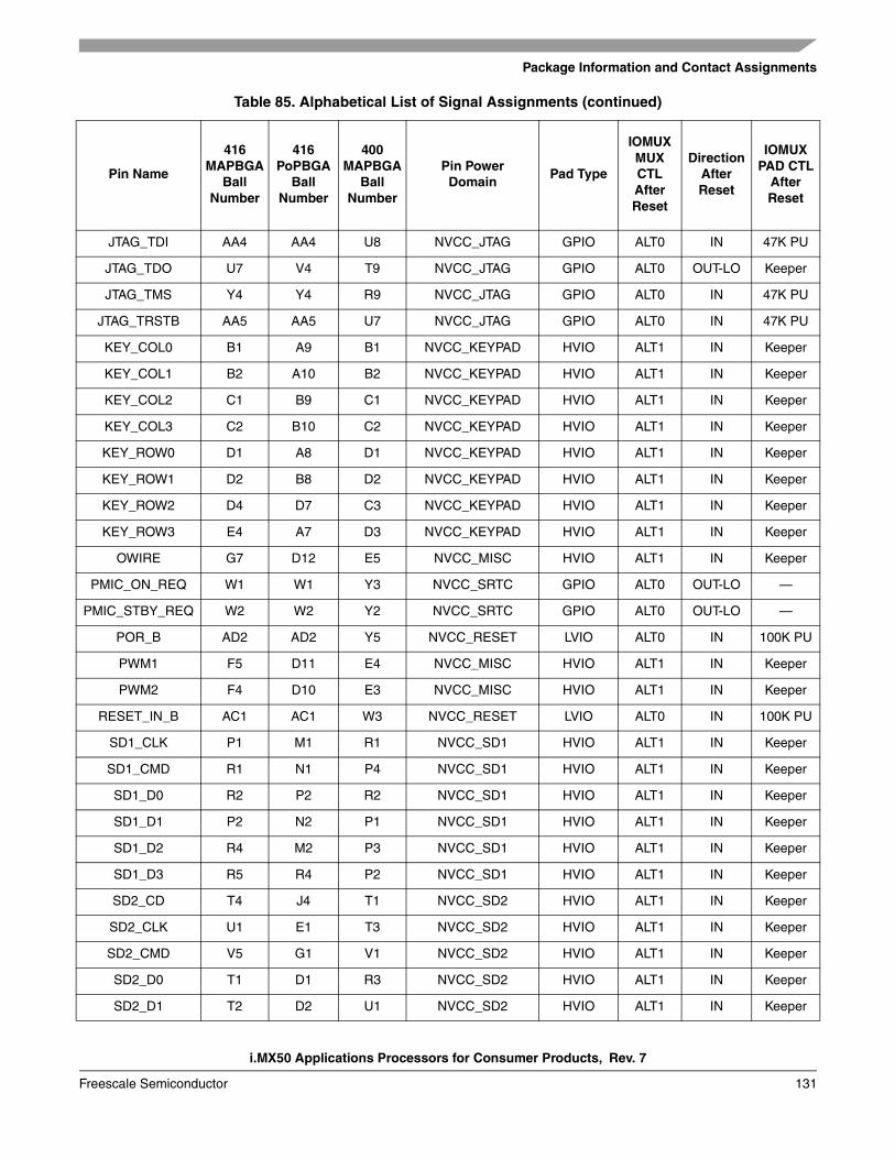
Package Information and Contact Assignments
i.MX50 Applications Processors for Consumer Products, Rev. 7
Freescale Semiconductor 131
JTAG_TDI AA4 AA4 U8 NVCC_JTAG GPIO ALT0 IN 47K PU
JTAG_TDO U7 V4 T9 NVCC_JTAG GPIO ALT0 OUT-LO Keeper
JTAG_TMS Y4 Y4 R9 NVCC_JTAG GPIO ALT0 IN 47K PU
JTAG_TRSTB AA5 AA5 U7 NVCC_JTAG GPIO ALT0 IN 47K PU
KEY_COL0 B1 A9 B1 NVCC_KEYPAD HVIO ALT1 IN Keeper
KEY_COL1 B2 A10 B2 NVCC_KEYPAD HVIO ALT1 IN Keeper
KEY_COL2 C1 B9 C1 NVCC_KEYPAD HVIO ALT1 IN Keeper
KEY_COL3 C2 B10 C2 NVCC_KEYPAD HVIO ALT1 IN Keeper
KEY_ROW0 D1 A8 D1 NVCC_KEYPAD HVIO ALT1 IN Keeper
KEY_ROW1 D2 B8 D2 NVCC_KEYPAD HVIO ALT1 IN Keeper
KEY_ROW2 D4 D7 C3 NVCC_KEYPAD HVIO ALT1 IN Keeper
KEY_ROW3 E4 A7 D3 NVCC_KEYPAD HVIO ALT1 IN Keeper
OWIRE G7 D12 E5 NVCC_MISC HVIO ALT1 IN Keeper
PMIC_ON_REQ W1 W1 Y3 NVCC_SRTC GPIO ALT0 OUT-LO —
PMIC_STBY_REQ W2 W2 Y2 NVCC_SRTC GPIO ALT0 OUT-LO —
POR_B AD2 AD2 Y5 NVCC_RESET LVIO ALT0 IN 100K PU
PWM1 F5 D11 E4 NVCC_MISC HVIO ALT1 IN Keeper
PWM2 F4 D10 E3 NVCC_MISC HVIO ALT1 IN Keeper
RESET_IN_B AC1 AC1 W3 NVCC_RESET LVIO ALT0 IN 100K PU
SD1_CLK P1 M1 R1 NVCC_SD1 HVIO ALT1 IN Keeper
SD1_CMD R1 N1 P4 NVCC_SD1 HVIO ALT1 IN Keeper
SD1_D0 R2 P2 R2 NVCC_SD1 HVIO ALT1 IN Keeper
SD1_D1 P2 N2 P1 NVCC_SD1 HVIO ALT1 IN Keeper
SD1_D2 R4 M2 P3 NVCC_SD1 HVIO ALT1 IN Keeper
SD1_D3 R5 R4 P2 NVCC_SD1 HVIO ALT1 IN Keeper
SD2_CD T4 J4 T1 NVCC_SD2 HVIO ALT1 IN Keeper
SD2_CLK U1 E1 T3 NVCC_SD2 HVIO ALT1 IN Keeper
SD2_CMD V5 G1 V1 NVCC_SD2 HVIO ALT1 IN Keeper
SD2_D0 T1 D1 R3 NVCC_SD2 HVIO ALT1 IN Keeper
SD2_D1 T2 D2 U1 NVCC_SD2 HVIO ALT1 IN Keeper
Table 85. Alphabetical List of Signal Assignments (continued)
Pin Name
416 MAPBGA
Ball Number
416 PoPBGA
Ball Number
400 MAPBGA
Ball Number
Pin PowerDomain
Pad Type
IOMUXMUX CTLAfterReset
DirectionAfter Reset
IOMUX PAD CTL
After Reset

i.MX50 Applications Processors for Consumer Products, Rev. 7
Package Information and Contact Assignments
Freescale Semiconductor132
SD2_D2 V1 F1 W2 NVCC_SD2 HVIO ALT1 IN Keeper
SD2_D3 V2 F2 T4 NVCC_SD2 HVIO ALT1 IN Keeper
SD2_D4 V4 G2 V2 NVCC_SD2 HVIO ALT1 IN Keeper
SD2_D5 U2 E2 U2 NVCC_SD2 HVIO ALT1 IN Keeper
SD2_D6 U4 H4 R4 NVCC_SD2 HVIO ALT1 IN Keeper
SD2_D7 U5 F4 W1 NVCC_SD2 HVIO ALT1 IN Keeper
SD2_WP T5 G4 T2 NVCC_SD2 HVIO ALT1 IN Keeper
SD3_CLK AD16 T1 Y14 NVCC_NANDF HVIO ALT1 IN Keeper
SD3_CMD AD17 T2 U16 NVCC_NANDF HVIO ALT1 IN Keeper
SD3_D0 AC15 V1 Y17 NVCC_NANDF HVIO ALT1 IN Keeper
SD3_D1 AC16 V2 V16 NVCC_NANDF HVIO ALT1 IN Keeper
SD3_D2 AC17 R1 T16 NVCC_NANDF HVIO ALT1 IN Keeper
SD3_D3 AA17 U2 U15 NVCC_NANDF HVIO ALT1 IN Keeper
SD3_D4 AA18 P1 W17 NVCC_NANDF HVIO ALT1 IN Keeper
SD3_D5 Y18 U1 U17 NVCC_NANDF HVIO ALT1 IN Keeper
SD3_D6 AA19 R2 V17 NVCC_NANDF HVIO ALT1 IN Keeper
SD3_D7 Y19 U4 T15 NVCC_NANDF HVIO ALT1 IN Keeper
SD3_WP AD15 T4 W16 NVCC_NANDF HVIO ALT1 IN Keeper
SSI_RXC J7 AD12 H4 NVCC_SSI HVIO ALT1 IN Keeper
SSI_RXD J5 AC14 F3 NVCC_SSI HVIO ALT1 IN Keeper
SSI_RXFS H7 AD13 G5 NVCC_SSI HVIO ALT1 IN Keeper
SSI_TXC J4 AC13 G3 NVCC_SSI HVIO ALT1 IN Keeper
SSI_TXD H5 AD14 G4 NVCC_SSI HVIO ALT1 IN Keeper
SSI_TXFS H4 AC12 H3 NVCC_SSI HVIO ALT1 IN Keeper
TEST_MODE AC2 AC2 U4 NVCC_RESET LVIO ALT0 IN 100K PD
UART1_CTS H2 B4 J1 NVCC_UART HVIO ALT1 IN Keeper
UART1_RTS J2 B3 K2 NVCC_UART HVIO ALT1 IN Keeper
UART1_RXD J1 A2 K1 NVCC_UART HVIO ALT1 IN Keeper
UART1_TXD H1 A3 H1 NVCC_UART HVIO ALT1 IN Keeper
UART2_CTS K2 B2 NVCC_UART HVIO ALT1 IN Keeper
Table 85. Alphabetical List of Signal Assignments (continued)
Pin Name
416 MAPBGA
Ball Number
416 PoPBGA
Ball Number
400 MAPBGA
Ball Number
Pin PowerDomain
Pad Type
IOMUXMUX CTLAfterReset
DirectionAfter Reset
IOMUX PAD CTL
After Reset

Package Information and Contact Assignments
i.MX50 Applications Processors for Consumer Products, Rev. 7
Freescale Semiconductor 133
UART2_RTS L2 C2 NVCC_UART HVIO ALT1 IN Keeper
UART2_RXD L1 C1 L2 NVCC_UART HVIO ALT1 IN Keeper
UART2_TXD K1 B1 L1 NVCC_UART HVIO ALT1 IN Keeper
UART3_RXD L4 E4 K3 NVCC_UART HVIO ALT1 IN Keeper
UART3_TXD K4 D4 J2 NVCC_UART HVIO ALT1 IN Keeper
UART4_RXD L5 D5 J3 NVCC_UART HVIO ALT1 IN Keeper
UART4_TXD K5 D6 H2 NVCC_UART HVIO ALT1 IN Keeper
USB_H1_DN AC10 AC10 W10 USB_H1_VDDA25, USB_H1_VDDA33
ANALOG50 — — —
USB_H1_DP AD10 AD10 Y10 USB_H1_VDDA25, USB_H1_VDDA33
ANALOG50 — — —
USB_H1_GPANAIO
Y11 AA17 U10 USB_H1_VDDA25, USB_H1_VDDA33
ANALOG25 — — —
USB_H1_RREFEXT
AA10 AA10 U9 USB_H1_VDDA25, USB_H1_VDDA33
ANALOG25 — — —
USB_H1_VBUS Y10 AA16 V9 USB_H1_VDDA25, USB_H1_VDDA33
ANALOG50 — — —
USB_OTG_DN AC8 AC8 W8 USB_OTG_VDDA25, USB_OTG_VDDA33
ANALOG50 — — —
USB_OTG_DP AD8 AD8 Y8 USB_OTG_VDDA25, USB_OTG_VDDA33
ANALOG50 — — —
USB_OTG_GPANAIO
Y7 AA14 V7 USB_OTG_VDDA25, USB_OTG_VDDA33
ANALOG25 — — —
USB_OTG_ID Y8 AA12 Y7 USB_OTG_VDDA25, USB_OTG_VDDA33
ANALOG25 — — —
USB_OTG_RREFEXT
AA8 AA8 W7 USB_OTG_VDDA25, USB_OTG_VDDA33
ANALOG25 — — —
USB_OTG_VBUS Y9 AA13 V8 USB_OTG_VDDA25, USB_OTG_VDDA33
ANALOG50 — — —
VREF M23 M23 K17 VDDO25 ANALOG — — —
WDOG G5 D9 F4 NVCC_MISC HVIO ALT1 IN —
XTAL AD5 AD5 Y6 VDD2P5 ANALOG — — —
Table 85. Alphabetical List of Signal Assignments (continued)
Pin Name
416 MAPBGA
Ball Number
416 PoPBGA
Ball Number
400 MAPBGA
Ball Number
Pin PowerDomain
Pad Type
IOMUXMUX CTLAfterReset
DirectionAfter Reset
IOMUX PAD CTL
After Reset

i.MX50 Applications Processors for Consumer Products, Rev. 7
Revision History
Freescale Semiconductor134
6 Revision HistoryTable 86 provides a revision history for this data sheet.
Table 86. i.MX50 Data Sheet Document Revision History
Rev.Number
Date Substantive Change(s)
Rev. 7 10/2013 • Added new part number information for parts with 1 GHz core frequencies: — MCIMX508CVK1B— MCIMX508CVM1B— MCIMX507CVM1B— MCIMX507CVK1BUpdated sections:— Section 1, “Introduction” — Table 1, “Ordering Information” — Table 11, “i.MX50 Operating Ranges”— Table 15, “Maximum Supply Current Consumption—ARM CLK = 1 GHz” (added)
Rev. 6 07/2013 • In Table 11, “i.MX50 Operating Ranges,” added VCC Stop mode ranges.
Rev. 5 05/2013 • In Table 11, “i.MX50 Operating Ranges,” changed VCC peripheral supply (LPM) minimum voltage from 0.9 V to 1 V, and changed nominal voltage from 0.95 V to 1.05 V.
Rev. 4 01/2013 • In Table 1, "Ordering Information," on page 7, added new part number information for MCIMX507CVK8B. • In Figure 27, "DTACK Read Access," on page 67, updated timing of EIM_DTACK.
Rev. 3 10/2012 • In Table 11, "i.MX50 Operating Ranges," on page 24:—Changed DDR clock rate for reduced performance mode (RPM) of VCC from 100 MHz to 133 MHz—Changed DDR clock rate for high performance mode (HPM) of VCC from 200 MHz to 266 MHz
Rev. 2 05/2012 • In Table 1, "Ordering Information," on page 7, added the following new part numbers: MCIMX508CZK8B, MCIMX503CVK8B, MCIMX503EVM8B, MCIMX502CVK8B, and MCIMX502EVM8B.
• In Table 1, "Ordering Information," on page 7, added a new column, Tjunction. • In Table 3, "Package Feature Comparison," on page 9, added a new row for 416 PoPBGA package. • Updated Figure 1, "i.MX50 System Block Diagram," on page 10 by removing “LDOx3” and “DC-DC 1.2V.” • In Table 5, "Special Signal Considerations," on page 17, updated details for the following signals:
DRAM_OPEN/DRAM_OPENFB and DRAM_SDODT0/DRAM_SDODT1 • In Table 5, "Special Signal Considerations," on page 17, added new rows for the following signals:
POP_EMMC_RST, POP_LPDDR2_ZQ0/ZQ1, POP_LPDDR2_1.8V, and POP_NAND_VCC. • Added Section 4.1.2.1, “13 x 13 mm MAPBGA Package Thermal Resistance Data.” • Added Section 4.1.2.2, “13 x 13 mm PoPBGA Package Thermal Resistance Data.” • Added Section 4.1.2.3, “17 x 17 mm MAPBGA Package Thermal Resistance Data.” • In Table 11, "i.MX50 Operating Ranges," on page 24, added footnotes for USB_OTG_VDDA25 and
USB_OTG_VDDA33. • In Table 78, "VBUS Comparators Thresholds," on page 101, changed VBUS input max current to 350 μA. • Added Section 5.2, “13 x 13 mm, 0.5 mm Pitch, 416 Pin PoPBGA Package Information.” • In Table 85, "Alphabetical List of Signal Assignments," on page 124:
—Added a new column “416 PoPBGA Ball Number”—Changed “USB_H1_VDDA” to “USB_H1_VDDA25, USB_H1_VDDA33”—Changed “USB_OTG_VDDA” to “USB_OTG_VDDA25, USB_OTG_VDDA33”
• Replace mDDR with LPDDR1 throughout the document.

Revision History
i.MX50 Applications Processors for Consumer Products, Rev. 7
Freescale Semiconductor 135
Rev. 1 10/2011 • Table 5, "Special Signal Considerations," on page 17 changed CHRG_DET_B to CHGR_DET_B. • Table 5, "Special Signal Considerations," on page 17 in the CHGR_DET_B signal remarks, added “The
maximum current leakage at this pin is 8.5 μA.” • Table 5, "Special Signal Considerations," on page 17 in the JTAG_MOD remarks, changed “pull-down”
to “pull-up, by default” and added “If JTAG port is not needed, the internal pull-up can be disabled in order to reduce supply current to the pin.”
• Table 14, "Maximum Supply Current Consumption—ARM CLK = 800 MHz," on page 27 in the 11th row under the Supply column, changed VDDO2P5 to VDDO25.
• Table 78, "VBUS Comparators Thresholds," on page 101 changed CHRG_DET_B to CHGR_DET_B. • Table 5, "Special Signal Considerations," on page 17 for 416 MAPBGA, DRAM_SDCLK_0 pin number
was changed to N24 and DRAM_SDCLK_0_B pin number was changed to M24. • Table 5, "Special Signal Considerations," on page 17 for 416 MAPBGA, DRAM_SDCLK_1 pin number
was changed to T20 and DRAM_SDCLK_1_B pin number was changed to R20. • Table 5, "Special Signal Considerations," on page 17 for 416 MAPBGA, DRAM_SDQS0 pin number was
changed to P23 and DRAM_SDQS0_B pin number was changed to P24. • Table 5, "Special Signal Considerations," on page 17 changed pad type of pin DRAM_CALIBRATION to
DRAMCALIB. • Table 5, "Special Signal Considerations," on page 17 changed pad type of pins DRAM_SDCLK_0,
DRAM_SDCLK_0_B, DRAM_SDCLK_1, DRAM_SDCLK_1_B, DRAM_SDQS0, DRAM_SDQS0_B, DRAM_SDQS1, DRAM_SDQS1_B, DRAM_SDQS2, DRAM_SDQS2_B, DRAM_SDQS3, and DRAM_SDQS3_B to DRAMCLK.
Rev. 0 07/2011 Initial release.
Table 86. i.MX50 Data Sheet Document Revision History (continued)
Rev.Number
Date Substantive Change(s)

Document Number: IMX50CECRev. 710/2013
Information in this document is provided solely to enable system and software
implementers to use Freescale products. There are no express or implied copyright
licenses granted hereunder to design or fabricate any integrated circuits based on the
information in this document.
Freescale reserves the right to make changes without further notice to any products
herein. Freescale makes no warranty, representation, or guarantee regarding the
suitability of its products for any particular purpose, nor does Freescale assume any
liability arising out of the application or use of any product or circuit, and specifically
disclaims any and all liability, including without limitation consequential or incidental
damages. “Typical” parameters that may be provided in Freescale data sheets and/or
specifications can and do vary in different applications, and actual performance may
vary over time. All operating parameters, including “typicals,” must be validated for each
customer application by customer’s technical experts. Freescale does not convey any
license under its patent rights nor the rights of others. Freescale sells products pursuant
to standard terms and conditions of sale, which can be found at the following address:
freescale.com/SalesTermsandConditions.
How to Reach Us:
Home Page: freescale.com
Web Support: freescale.com/support
Freescale, the Freescale logo, and Energy Efficient Solutions logo are trademarks of
Freescale Semiconductor, Inc., Reg. U.S. Pat. & Tm. Off. All other product or service
names are the property of their respective owners. ARM and Cortex are the registered
trademarks of ARM Limited. NEON is the trademark of ARM Limited.
© 2011–2013 Freescale Semiconductor, Inc.