improving the resolution limit of electron beam lithography
TRANSCRIPT

[email protected] 1Litho2006 – Marseille, 28.06.2006
Improving the Resolution Limit of Improving the Resolution Limit of Improving the Resolution Limit of Improving the Resolution Limit of Electron Beam LithographyElectron Beam LithographyElectron Beam LithographyElectron Beam Lithography
J. Bolten, T. Wahlbrink, M.C. Lemme, H. Kurz

[email protected] Litho2006 – Marseille, 28.06.2006
Contents
� AMO GmbH / AMICA
� Why electron beam lithography?
� Improving electron beam
lithography
� Applications
� Summary & Outlook

[email protected] Litho2006 – Marseille, 28.06.2006
Contents
� AMO GmbH / AMICA
� Why electron beam lithography?
� Improving electron beam
lithography
� Applications
� Summary & Outlook

[email protected] Litho2006 – Marseille, 28.06.2006
AMO GmbH / AMICA
� Spin-Off of RWTH Aachen University
� “Research foundry”
� Operational since 1997
� 43 Employees (29 Nanolab AMICA, 10 AMO Systems)
� 70% joint research, 30% sales
� 6 to 10 concurrent R&D projects
� 400 m² class 10-1000 clean room, highly flexible
� Advanced nanofabrication facilities

[email protected] Litho2006 – Marseille, 28.06.2006
Information
Life Energy
AMO
RWTH
Basics
Technology
transfer
Markets
Basic research on semiconductors(Processes, technology and devices)
Nanotechnology
Mission of AMO

[email protected] Litho2006 – Marseille, 28.06.2006
Research projects and collaboration
� Recent projects:
� NaPa
� CellPROM
� Sinano / PullNano
� OLAS
� Souvenir
� Krismos
� …
� Partners
� AMD
� IBM
� Infineon
� Qimonda
� Raith GmbH
� Vistec
� EV Group
� RWTH Aachen
� …

[email protected] Litho2006 – Marseille, 28.06.2006
Fields of research
� Novel gate stack materials
� metal gates
� high-k materials
� Nano transistors, e. g. triple gate MOSFETS
� Siliconizing photonics
� Fabrication of nanostructures for life
science applications
� Nanoimprint lithography (NIL)
� Process development for electron
beam lithography (EBL)

[email protected] Litho2006 – Marseille, 28.06.2006
Contents
� AMO GmbH, AMICA
� Why electron beam lithography?
� Improving electron beam
lithography
� Applications
� Summary & Outlook
[email protected] Litho2006 – Marseille, 28.06.2006
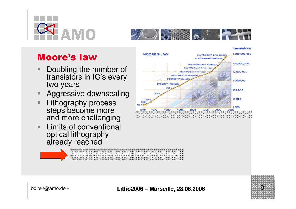
Moore’s law
� Doubling the number of transistors in IC’s every two years
� Aggressive downscaling
� Lithography process steps become more and more challenging
� Limits of conventional optical lithography already reached
Source: www.intel.com
Next generation lithography?

[email protected] Litho2006 – Marseille, 28.06.2006
Next generation lithography?
� Possible candidates for next generation
lithography (NGL):
� EUV lithography (EUVL)
� Nanoimprint lithography
� Both rely on EBL for mask (EUVL) and
template (NIL) fabrication
Whatever technique will be chosen forNGL, EBL will be an important part of it
[email protected] Litho2006 – Marseille, 28.06.2006
Challenges for EBL
� Ultra high resolution well below 10nm needed
� Aspect ratios for such small resist structures have to besufficient for pattern transfer
� Surface and line edge roughness of resist structures haveto be kept as small as possible
� To achieve this, conventional processing might not besufficient
New processing techniques needed to further improve resolution and aspectratio and to decrease resist roughness

[email protected] Litho2006 – Marseille, 28.06.2006
Contents
� AMO GmbH, AMICA
� Why electron beam lithography?
� Improving electron beam
lithography
� Applications
� Summary & Outlook

[email protected] Litho2006 – Marseille, 28.06.2006
EBL process
� EBL tool� Leica EBPG 5000 operated @ 100kV� Minimal beam step size: 5nm� Stage interferometer resolution: ~5nm� Margin for improvements is small
� Choice of resist material� Well-known resists with potential for
further improvements, e.g. poly(methylmethacrylate) (PMMA) � Novel resist materials, e. g. hydrogen silsesquioxane (HSQ)
� Development process� Megasonic-assisted development (MAD)
� Drying process after development� Supercritical resist drying (SRD)

[email protected] Litho2006 – Marseille, 28.06.2006
Megasonic-assisted development I
� Conventional dip development� Thick viscous boundary layer at resist/developer interface
� Long development times neeeded
� Acoustic agitation during development process step� Reduces thickness of boundary layer
� Ultrasonic agitation (20-350 kHz)� Thickness of boundary layer: ~4 µm
� Tends to damage resist structures
� Megasonic agitation (700 kHz – 1 MHz)� Thickness of boundary layer: <1 µm
� Applicable for both positive and negative tone resist materials
� Best results for positive tone resist (PMMA)

[email protected] Litho2006 – Marseille, 28.06.2006
Megasonic-assisted development II
Dense holes in ~700nm PMMA
resist, developed without…
…and with megasonic agitationduring development
MAD
D. Küpper et al, JVST B, to be published 2006
[email protected] Litho2006 – Marseille, 28.06.2006
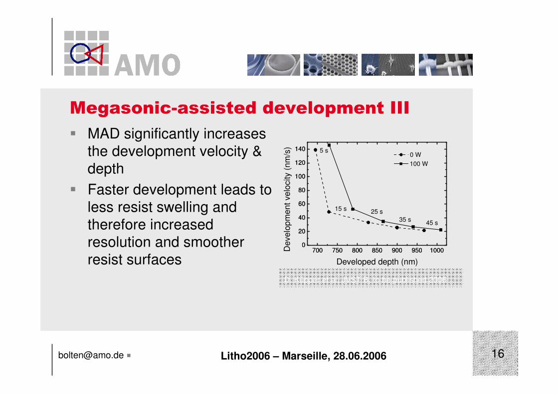
Megasonic-assisted development III
� MAD significantly increases
the development velocity &
depth
� Faster development leads to
less resist swelling and
therefore increased
resolution and smoother
resist surfaces700 750 800 850 900 950 1000
0
20
40
60
80
100
120
140
700 750 800 850 900 950 10000
20
40
60
80
100
120
140
45 s35 s
25 s15 s
100 W
5 s
Develo
pm
ent ve
locity (
nm
/s)
Developed depth (nm)
0 W
D. Küpper et al, JVST B, to be published 2006

[email protected] Litho2006 – Marseille, 28.06.2006
D. Küpper et al, JVST B, to be published 2006
Megasonic-assisted development IV
Nano holes with diameters of ~6nm, sample has been coated with Cr to avoid static during SEM inspection
� MAD significantlyimproves:� Development homogeniety
� Development depth
� Roughness
� Resolution
[email protected] Litho2006 – Marseille, 28.06.2006
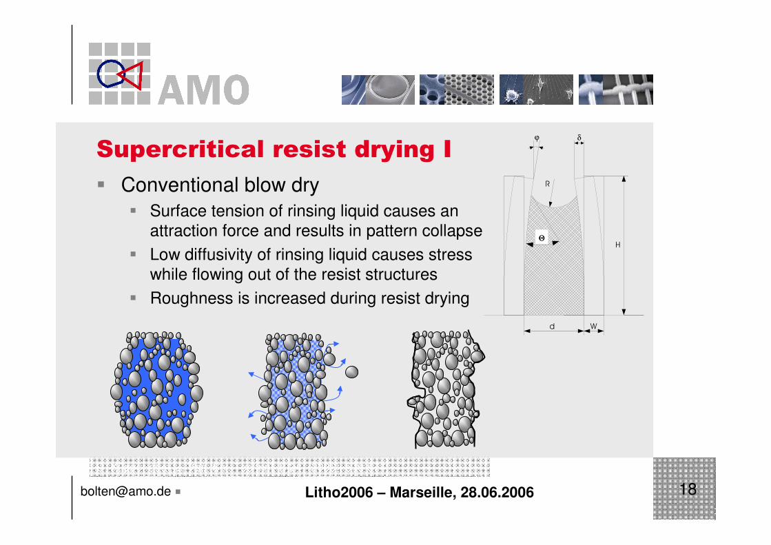
Supercritical resist drying I
� Conventional blow dry
� Surface tension of rinsing liquid causes an attraction force and results in pattern collapse
� Low diffusivity of rinsing liquid causes stresswhile flowing out of the resist structures
� Roughness is increased during resist drying
d
H
ϕ δ
ΘΘ
W
R
D. Küpper et al, J. Vac. Sci. Technol. B 24, (2006), 570-574

[email protected] Litho2006 – Marseille, 28.06.2006
Supercritical resist drying II
� Rinsing liquid is replaced by supercritical CO2
� Why CO2?
� Chemically inert, environmental friendly
� In supercritial state : Reduced surface tension, high diffusivity
� Chamber pressure and temperature:7.38 MPa @ 35°C
� Best results for HSQ (negative tone resist)
Reduced stress for resist structuresduring the drying process

[email protected] Litho2006 – Marseille, 28.06.2006
…and with linewidths of ~20nm,
dried with SRD
HSQ lines with linewidths of
~40nm, dried without SRD …
Supercritical resist drying III
SRD
T. Wahlbrink et al, Micro. Eng. 83 (2006), 1124-1127

[email protected] Litho2006 – Marseille, 28.06.2006
Supercritical resist drying IV
HSQ lines with linewidths of ~20nm, aspect ratio ~40
� SRD improves:
� max. aspect ratio (AR) of resist structures
� depending on resistthickness the AR cannearly be doubled usingSRD
T. Wahlbrink et al, Micro. Eng. 83 (2006), 1124-1127

[email protected] Litho2006 – Marseille, 28.06.2006
Supercritical resist drying V
� SRD improves:
� Surface and lineedge roughnessby up to 20%
380 400 420 440 460 480 500 520 5403.0
3.5
4.0
4.5
5.0
5.5
6.0
6.5
7.0
7.5
380 400 420 440 460 480 500 520 5403.0
3.5
4.0
4.5
5.0
5.5
6.0
6.5
7.0
7.5
380 400 420 440 460 480 500 520 5403.0
3.5
4.0
4.5
5.0
5.5
6.0
6.5
7.0
7.5
380 400 420 440 460 480 500 520 5403.0
3.5
4.0
4.5
5.0
5.5
6.0
6.5
7.0
7.5
380 400 420 440 460 480 500 520 5403.0
3.5
4.0
4.5
5.0
5.5
6.0
6.5
7.0
7.5
380 400 420 440 460 480 500 520 5403.0
3.5
4.0
4.5
5.0
5.5
6.0
6.5
7.0
7.5
H2O rinse + IPA rinse, SCD (CO2)
Linear fit
Surf
ace R
oughness,
rms σ
(nm
)
Dose (µC/cm2)
H2O rinse + IPA rinse, N-blow
Linear fit
H2O rinse, N-blow
Linear fit
Both increased ARs and decreasedroughness lead to higher resolution
D. Küpper et al, J. Vac. Sci. Technol. B 24, (2006), 570-574

[email protected] Litho2006 – Marseille, 28.06.2006
Contents
� AMO GmbH, AMICA
� Why electron beam lithography?
� Improving electron beam
lithography
� Applications
� Summary & Outlook

[email protected] Litho2006 – Marseille, 28.06.2006
Applications
� Lithography for transfer of
nano patterns
Source: AMO GmbH

[email protected] Litho2006 – Marseille, 28.06.2006
Applications
� Ring resonator structures
„all optical switch“
Source: AMO GmbH

[email protected] Litho2006 – Marseille, 28.06.2006
Applications
� Nanowire structures, e.g. for
sensor applications
Source: AMO GmbH

[email protected] Litho2006 – Marseille, 28.06.2006
Applications
� Nano transistors
Triple gate MOSFETS
Lemme et al., SSE, 2004

[email protected] Litho2006 – Marseille, 28.06.2006
Contents
� AMO GmbH / AMICA
� Why electron beam lithography?
� Improving electron beam
lithography
� Applications
� Summary & Outlook

[email protected] Litho2006 – Marseille, 28.06.2006
Summary & Outlook
� EBL will be an important part of NGL
� Resolution well below 10nm will be needed
� MAD and SRD have demonstrated their potential
concerning resolution improvements in this regime
� Further investigations into both techniques have to bedone to explore their limits
� Novel resist materials sensitive to electron beam
exposure should be investigated
[email protected] Litho2006 – Marseille, 28.06.2006
Acknowledgments
� European Commission
� German ministry of education and research (BMBF)
� Our partners in our research projects

[email protected] Litho2006 – Marseille, 28.06.2006
Thank you.
You want to know more about us? Please talk to one of our representatives or visit our website:
www.amo.de