improved models for dc-dc converters · the boost converter has an output voltage that is higher...
TRANSCRIPT

Improved Models for DC-DC Converters
Bengt Johansson
Licentiate Thesis
Department of Industrial Electrical Engineering and Automation

ii
Department of Industrial Electrical Engineering and Automation Lund University P.O. Box 118 SE-221 00 LUND SWEDEN http://www.iea.lth.se ISBN 91-88934-29-2 CODEN:LUTEDX/(TEIE-1037)/1-365/(2003) ©Bengt Johansson, 2003 Printed in Sweden by Media-Tryck Lund University Lund, 2003

iii
Abstract
To obtain high performance control of a dc-dc converter, a good model
of the converter is needed. It is suitable to consider the load to be included in the converter model since it usually affects the dynamics. The load is often the most variable part of this system. If the load current and the output voltage are measured there are good possibilities to obtain a good model of the load on-line. Adaptive control can then be applied to improve the control.
In peak current-mode control, the output voltage and the inductor current are measured and utilized by the controller. This thesis analyses some properties that can be obtained if the load current is also measured and utilized for control. Accurate expressions for the control-to-output transfer function, the output impedance, and the audio susceptibility are derived for the buck, boost, and buck-boost converters operated in continuous conduction mode in the case where the load is a linear resistor. If the measured load current is utilized properly by the controller, the output impedance becomes low and the control-to-output transfer function becomes almost invariant for different loads. The use of load current acts as a feedforward term if the load is a current source. However, if the load is a resistor the load current is influenced by changes in the output voltage and the stability is affected. Therefore, the use of load current is not a feedforward action in this case. Instead it can be seen as gain scheduling, which can be considered a special case of adaptive control.
In the thesis it is also shown that the two published models for current-mode control, Ridley (1991) and Tan and Middlebrook (1995), give accurate expressions for the control-to-output transfer function and the output impedance but not for the audio susceptibility. A novel model for the audio susceptibility is presented and it is used to improve the two published models.
Most of the results in the thesis are validated by comparing the frequency responses predicted by the expressions and switched large-signal simulation models.

iv

v
Acknowledgements
First of all, I would like to thank my supervisors Professor Gustaf Olsson
and Dr Matz Lenells for guidance during my work and for comments on the draft of this thesis. Thanks also to Dr Per Karlsson for reading and commenting the draft.
Furthermore, I would like to thank Johan Fält, Ericsson Microwave Systems AB, and Mikael Appelberg, Ericsson Power Modules AB, for discussions about practical problems with dc-dc converters and for helping me with measurements.
I would also like to thank the staff at the Department of Technology, University College of Kalmar, and the staff at the Department of Industrial Electrical Engineering and Automation (IEA), Lund University, who have helped me in many ways.
This work has been financially supported by The Knowledge Foundation, University College of Kalmar, and Ericsson Microwave Systems AB.
Finally, I would like to thank my family for supporting me.
Kalmar, October 2003 Bengt Johansson

vi

vii
Notation
Frequently used signals and parameters are presented with name and
description in the list below. Signals and parameters that only appear in one of the chapters are not included in the list. The names of signals consist of lower-case letters. However, exceptions are made for the subscript part of the names. The names of the signals are also used to denote their dc values but capital letters are used in this case. However, the letters in the subscript part are not changed. The dc value names are not included in the list.
Name Description
C Capacitance of the capacitor d Duty cycle
'd dd −=1'
ci Current reference
capi Capacitor current
ei External ramp used for slope compensation
inji Current injected into the output stage
Li Inductor current
loadi Load current
fk Input voltage feedforward gain (see Section 3.4)
rk Output voltage feedforward gain (see Section 3.4) L Inductance of the inductor
1m Slope of the inductor current while the transistor in on
2m− Slope of the inductor current while the transistor in off
cm Relative slope of the external ramp, 11 MMm ec +=
eM Slope of the external ramp R Resistance of the load resistor
cR Equivalent Series Resistance (ESR) of the capacitor
sT Switching period

viii
gv Input voltage
ov Output voltage
refv Voltage reference δ Control signal of the transistor driver
nω Half the switching frequency, sn Tπω = Signals are often divided into a dc part and an ac part. The ac part is
denoted by using the hat-symbol (^). As mentioned earlier, the dc part is denoted by using capital letters. To explicitly denote that a signal is a function of time, the variable t is added to the name, i.e. )(tnamesignal . The sampled version of a continuous-time signal is denoted by replacing the variable t with n . The Laplace transform of a continuous-time signal is denoted by replacing the variable t with s . The Z-transform of a discrete-time signal is denoted by replacing the variable n with z .
The notation is to some extent chosen such that it is compatible with the one used by Ridley (1991).

ix
Contents
CHAPTER 1 INTRODUCTION........................................................1
1.1 BACKGROUND ..........................................................................1 1.2 MOTIVATION FOR THE WORK ..................................................5 1.3 MAIN CONTRIBUTIONS.............................................................7 1.4 A GUIDE FOR THE READER AND THE OUTLINE OF THE
THESIS ......................................................................................9 1.5 PUBLICATIONS........................................................................10
CHAPTER 2 STATE-SPACE AVERAGING ................................11
2.1 INTRODUCTION.......................................................................11 2.2 OPERATION OF THE BUCK CONVERTER .................................12 2.3 MODEL OF THE BUCK CONVERTER........................................15 2.4 SIMULATION OF A BUCK CONVERTER ...................................33 2.5 OPERATION OF THE BOOST CONVERTER ...............................39 2.6 MODEL OF THE BOOST CONVERTER ......................................44 2.7 SIMULATION OF A BOOST CONVERTER..................................55 2.8 OPERATION OF THE BUCK-BOOST CONVERTER.....................58 2.9 MODEL OF THE BUCK-BOOST CONVERTER ...........................61 2.10 SIMULATION OF A BUCK-BOOST CONVERTER.......................71 2.11 SUMMARY AND CONCLUDING REMARKS ..............................74
CHAPTER 3 CURRENT-MODE CONTROL ...............................77
3.1 INTRODUCTION.......................................................................77 3.2 OPERATION OF CURRENT-MODE CONTROL...........................78 3.3 AN ACCURATE CONTROL-TO-CURRENT TRANSFER
FUNCTION...............................................................................83 3.4 THE RIDLEY AND TAN MODELS APPLIED TO THE BUCK
CONVERTER ...........................................................................87

x
3.5 A COMPARISON OF THE TWO MODELS AND THE SIMULATION RESULTS......................................................... 109
3.6 THE RIDLEY MODEL APPLIED TO THE BOOST CONVERTER 115 3.7 THE RIDLEY MODEL APPLIED TO THE BUCK-BOOST
CONVERTER......................................................................... 125 3.8 SUMMARY AND CONCLUDING REMARKS............................ 136
CHAPTER 4 A NOVEL MODEL ................................................. 139
4.1 CHAPTER SURVEY ............................................................... 139 4.2 A NOVEL MODEL FOR THE AUDIO SUSCEPTIBILITY............ 139 4.3 AUDIO SUSCEPTIBILITY OF THE BUCK CONVERTER............ 154 4.4 AUDIO SUSCEPTIBILITY OF THE BOOST CONVERTER.......... 161 4.5 AUDIO SUSCEPTIBILITY OF THE BUCK-BOOST CONVERTER175 4.6 SUMMARY AND CONCLUDING REMARKS............................ 183
CHAPTER 5 IMPROVED MODELS........................................... 185
5.1 CHAPTER SURVEY ............................................................... 185 5.2 IMPROVED EXPRESSIONS FOR THE BUCK CONVERTER ....... 185 5.3 IMPROVED EXPRESSION FOR THE BOOST CONVERTER ....... 188 5.4 IMPROVED EXPRESSION FOR THE BUCK-BOOST
CONVERTER......................................................................... 196 5.5 SUMMARY AND CONCLUDING REMARKS............................ 205
CHAPTER 6 APPROXIMATIONS OF OBTAINED EXPRESSIONS............................................................................... 207
6.1 CHAPTER SURVEY ............................................................... 207 6.2 APPROXIMATE MODEL FOR THE BUCK CONVERTER........... 207 6.3 APPROXIMATE MODEL FOR THE BOOST CONVERTER ......... 229 6.4 APPROXIMATE MODEL FOR THE BUCK-BOOST
CONVERTER......................................................................... 241 6.5 SUMMARY AND CONCLUDING REMARKS............................ 258
CHAPTER 7 USING LOAD CURRENT FOR CONTROL....... 259
7.1 CHAPTER SURVEY ............................................................... 259 7.2 A REVIEW ............................................................................ 259 7.3 PRINCIPAL PROPERTIES ....................................................... 262 7.4 PROPERTIES OF THE BUCK CONVERTER.............................. 272 7.5 PROPERTIES OF THE BOOST CONVERTER ............................ 298 7.6 PROPERTIES OF THE BUCK-BOOST CONVERTER ................. 325 7.7 SUMMARY AND CONCLUDING REMARKS............................ 336
xi
CHAPTER 8 SUMMARY ..............................................................341
8.1 RESULTS...............................................................................341 8.2 FUTURE WORK.....................................................................344
CHAPTER 9 ERRATA FOR THREE PAPERS ..........................345
9.1 PAPER 1 ................................................................................346 9.2 PAPER 2 ................................................................................347 9.3 PAPER 3 ................................................................................348
CHAPTER 10 REFERENCES.......................................................351

xii

1
Chapter 1 Introduction
This thesis is concerned with the modeling and control of dc-dc converters with current-mode control. Special focus is on using load current measurements for control.
In this first chapter, the background of the problem is described, the motivation for the work is presented and the contributions of the thesis are outlined.
1.1 Background
DC-DC Converters
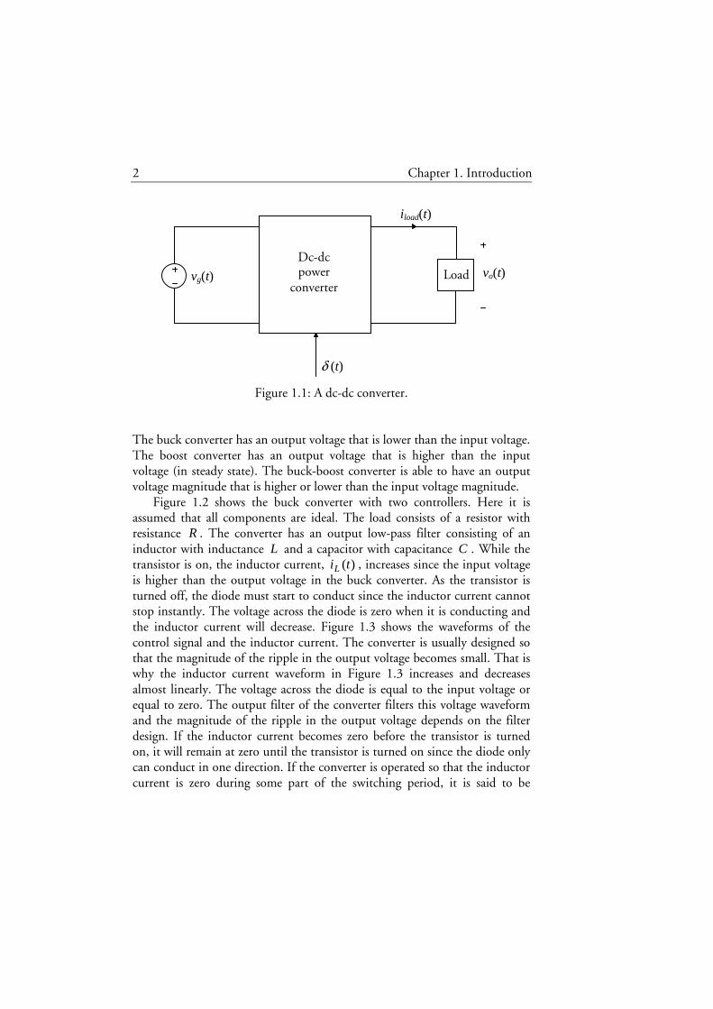
The principal schematic of a dc-dc converter is shown in Figure 1.1. It converts a dc input voltage, )(tvg , to a dc output voltage, )(tvo , with a magnitude other than the input voltage (Erickson and Maksimovic, 2000, Section 1.1). The converter often includes one (or several) transistor in order to control the output voltage, using the control signal )(tδ .
It is desirable that the conversion be made with low losses in the converter. Therefore, the transistor is not operated in its linear interval. Instead, it is operated as a switch and the control signal is binary. While the transistor is on, the voltage across it is low which means that the power loss in the transistor is low. While the transistor is off, the current through it is low and the power loss is also low. To obtain low losses, resistors are avoided in the converters. Capacitors and inductors are used instead since they ideally do not have any losses.
The electrical components can be combined and connected to each other in different ways, called topologies, each one having different properties. The buck, boost, and buck-boost converters are three basic converter topologies.
2 Chapter 1. Introduction
Figure 1.1: A dc-dc converter.
The buck converter has an output voltage that is lower than the input voltage. The boost converter has an output voltage that is higher than the input voltage (in steady state). The buck-boost converter is able to have an output voltage magnitude that is higher or lower than the input voltage magnitude.
Figure 1.2 shows the buck converter with two controllers. Here it is assumed that all components are ideal. The load consists of a resistor with resistance R . The converter has an output low-pass filter consisting of an inductor with inductance L and a capacitor with capacitance C . While the transistor is on, the inductor current, )(tiL , increases since the input voltage is higher than the output voltage in the buck converter. As the transistor is turned off, the diode must start to conduct since the inductor current cannot stop instantly. The voltage across the diode is zero when it is conducting and the inductor current will decrease. Figure 1.3 shows the waveforms of the control signal and the inductor current. The converter is usually designed so that the magnitude of the ripple in the output voltage becomes small. That is why the inductor current waveform in Figure 1.3 increases and decreases almost linearly. The voltage across the diode is equal to the input voltage or equal to zero. The output filter of the converter filters this voltage waveform and the magnitude of the ripple in the output voltage depends on the filter design. If the inductor current becomes zero before the transistor is turned on, it will remain at zero until the transistor is turned on since the diode only can conduct in one direction. If the converter is operated so that the inductor current is zero during some part of the switching period, it is said to be
δ (t)
vg(t)
iload(t)
vo(t) Load Dc-dcpower
converter

Chapter 1. Introduction 3
Figure 1.2: The buck converter with a current controller and a voltage
controller.
Figure 1.3: The waveforms of the control signal and the inductor current. operated in discontinuous conduction mode. Otherwise, it is operated in continuous conduction mode.
The switching period, sT , of the converter is determined by the control signal )(tδ , as shown in Figure 1.3. In this figure, the switching period is held constant. The average output voltage is controlled by changing the width of the pulses. In Figure 1.3, the falling edge is controlled i.e. when the
L
vo(t) C
Driver
ic(t)
R
δ (t)
iload(t)
Currentcontroller
Voltage controller
Vref
iL(t)
vg(t)
t 0 Tsd(t) Ts
iL(t)
t
δ (t)

4 Chapter 1. Introduction
transistor should turn off. The duty cycle, )(td , is a real value in the interval 0 to 1 and it is equal to the ratio of the width of a pulse to the switching period. The duty cycle is actually a discrete-time signal.
State-Space Averaging
The converter acts as a time-invariant system while the transistor is on. While the transistor is off the converter acts as another time-invariant system and if the inductor current reaches zero, the converter acts as yet another time-invariant system. If the transistor is controlled as described previously, the converter can be described as switching between different time-invariant systems during the switching period. Consequently, the converter can be modeled as a time-variant system. State-space averaging (Middlebrook and Cuk, 1976) is one method to approximate this time-variant system with a linear continuous-time time-invariant system. This method uses the state-space description of each time-invariant system as a starting point. These state-space descriptions are then averaged with respect to their duration in the switching period. The averaged model is nonlinear and time-invariant and has the duty cycle, )(td , as the control signal instead of )(tδ . This model is finally linearized at the operating point to obtain a small-signal model. From the model we will extract three major transfer functions:
• The control-to-output transfer function describes how a change in the
control signal affects the output voltage. • The output impedance describes how a change in the load current affects
the output voltage. • The audio susceptibility describes how a change in the input voltage
affects the output voltage.
Current-Mode Control
Figure 1.2 shows the buck converter controlled by two control loops. The inductor current is fed back to the current controller in the inner loop and the output voltage is fed back to the voltage controller in the outer loop. This control method is called current-mode control. (The name current controller is used instead of current modulator in this thesis, see Section 3.2.) Assume that the outer loop is not present. The system is then a closed loop system since the inductor current is fed back. If the outer loop is added, a new closed loop is obtained. The control signal from the outer loop acts as the reference

Chapter 1. Introduction 5
signal for the current controller. The three transfer functions mentioned above will in general be different for the new closed loop system.
The current controller controls the inductor current. This can be made in different ways. One way is to control the peak value of the inductor current in each switching period. Ridley (1991) and Tan and Middlebrook (1995) have presented two models for current-mode control. (The voltage controller is actually excluded.) The main difference between the two models is the modeling of the current loop gain.
The output voltage is fed back to the voltage controller so that the output voltage is kept near the voltage reference signal refV (see Figure 1.2). The voltage controller controls the reference signal of the current controller, )(tic . An alternative is to let the voltage controller control the duty cycle directly. This means that the measurement of the inductor current and the current controller are not needed. This control method is called voltage-mode control.
1.2 Motivation for the Work
Many aspects must be considered in the case where a converter is to be designed. One such aspect is keeping the output voltage in the specified voltage interval. Here are some examples of changes that can decrease the variation of the output voltage:
• Change the properties of some of the components in the converter, e.g.
increase the capacitance of the capacitor. • Change the converter topology. • Change to a more advanced controller. • Increase the number of signals that are measured and used by the
controller.
Each one of these changes has one or several disadvantages such as:
• Higher cost. • Increased weight and volume. • Lower reliability. • Lower efficiency (see Poon, Tse, and Liu (1999)).
Therefore, the change or changes that are most suitable depend to a large extent on the converter specification at hand.
6 Chapter 1. Introduction
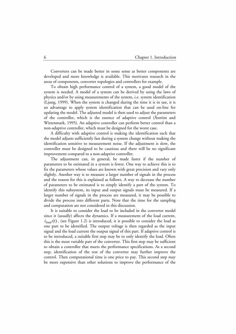
Converters can be made better in some sense as better components are developed and more knowledge is available. This motivates research in the areas of components, converter topologies and controllers for example.
To obtain high performance control of a system, a good model of the system is needed. A model of a system can be derived by using the laws of physics and/or by using measurements of the system, i.e. system identification (Ljung, 1999). When the system is changed during the time it is in use, it is an advantage to apply system identification that can be used on-line for updating the model. The adjusted model is then used to adjust the parameters of the controller, which is the essence of adaptive control (Åström and Wittenmark, 1995). An adaptive controller can perform better control than a non-adaptive controller, which must be designed for the worst case.
A difficulty with adaptive control is making the identification such that the model adjusts sufficiently fast during a system change without making the identification sensitive to measurement noise. If the adjustment is slow, the controller must be designed to be cautious and there will be no significant improvement compared to a non-adaptive controller.
The adjustment can, in general, be made faster if the number of parameters to be estimated in a system is fewer. One way to achieve this is to fix the parameters whose values are known with great precision and vary only slightly. Another way is to measure a larger number of signals in the process and the reason for this is explained as follows. A way to decrease the number of parameters to be estimated is to simply identify a part of the system. To identify this subsystem, its input and output signals must be measured. If a larger number of signals in the process are measured, it may be possible to divide the process into different parts. Note that the time for the sampling and computation are not considered in this discussion.
It is suitable to consider the load to be included in the converter model since it (usually) affects the dynamics. If a measurement of the load current,
)(tiload , (see Figure 1.2) is introduced, it is possible to consider the load as one part to be identified. The output voltage is then regarded as the input signal and the load current the output signal of this part. If adaptive control is to be introduced, a suitable first step may be to only identify the load. Often this is the most variable part of the converter. This first step may be sufficient to obtain a controller that meets the performance specifications. As a second step, identification of the rest of the converter may further improve the control. Then computational time is one price to pay. This second step may be more expensive than other solutions to improve the performance of the

Chapter 1. Introduction 7
closed loop system. This discussion motivates the research in identification of the load.
As mentioned above, the output voltage and the load current should be measured to obtain fast load identification. There are several papers that suggest that the load current should be measured and utilized for control of the converter and they show what properties are obtained. Two of these papers are mentioned here. The output voltage and the inductor current are assumed to be measured besides the load current in these two papers.
Redl and Sokal (1986) show that the transient in the output voltage due to a step change in the load can be much reduced. They call the use of the measured load current feedforward. For a definition of feedforward, see Åström and Hägglund (1995, Section 7.3). Redl and Sokal also show that the control-to-output transfer function does not change when this feedforward is introduced.
The dc gain of the control-to-output transfer function normally depends on the load. Hiti and Borojevic (1993) use the measured load current to make the control-to-output transfer function invariant for different loads at dc for the boost converter. Hiti and Borojevic thus show that the control-to-output transfer function changes when the use of measured load current is introduced. The control Hiti and Borojevic use turns out to be exactly the same as the one Redl and Sokal propose for the boost converter.
To summarize, Redl and Sokal show that the control-to-output transfer function does not change when the use of measured load current is introduced while Hiti and Borojevic show that it does change. It thus seems to be a contradiction. Since the output voltage and the load current are assumed to be measured in the two papers, the analysis may be connected to identification of the load in some way. Therefore, it is motivated to investigate this possible connection and contradiction before the work with identification of the load starts.
1.3 Main Contributions
Some of the properties that can be obtained using measured load current for control are analyzed in this thesis. The analysis is only made for the case where current-mode control is used. An accurate model is used in the case where the load is a linear resistor.
1. The analysis confirms that low output impedance can be obtained.

8 Chapter 1. Introduction
2. The analysis shows that in the case where the load is a current source, i.e. the load current is independent of the output voltage, the following properties are obtained: • The use of measured load current for control is feedforward. • The control-to-output transfer function does not change when this
feedforward is introduced. 3. The analysis shows that in the case where the load is a linear resistor, the
following properties are obtained: • The control-to-output transfer function can change when the
measured load current is introduced for control. • The converter can become unstable when the measured load current
is introduced for control. • The control-to-output transfer function can be almost invariant for
different linear resistive loads if the measured load current is used for control. This is especially the case for the buck converter.
• The use of measured load current for control is not feedforward. It can instead be seen as gain scheduling, which can be considered a special case of adaptive control (Åström and Wittenmark, 1995, Chapter 9).
In the thesis it is also shown that the two published models for current-
mode control, Ridley (1991) and Tan and Middlebrook (1995), give accurate expressions for the control-to-output transfer function and the output impedance but not for the audio susceptibility. A novel model for the audio susceptibility is presented and it is used to improve the Ridley and Tan models. The novel model is in some cases inaccurate at low frequencies but the improvements are made in such a way that this shortcoming is not transferred to the improved models. The improved models are accurate.
Accurate (continuous-time) expressions for the control-to-output transfer function, the output impedance, and the audio susceptibility are in this thesis derived for dc-dc converters that meet the following specifications:
• The converter topology is buck, boost or buck-boost. • The converter is operated in continuous conduction mode. • Current-mode control with constant switching frequency and peak-
current command is used. • The load is a linear resistor.

Chapter 1. Introduction 9
1.4 A Guide for the Reader and the Outline of the Thesis
A Guide for the Reader
If the reader is a designer of dc-dc converters and is about to use measured load current for the controller, it is recommended that Chapter 7 is read since it will increase the understanding of what properties can be expected. However, if the converter topology is buck (-derived), Section 7.5 and Section 7.6 can be omitted and if the converter topology is boost (-derived), Section 7.6 can be omitted. Section 7.6 should only be read if the converter topology is buck-boost (-derived).
The accurate transfer functions for current-mode control that are used as a basis for the analysis in Chapter 7 are derived throughout Chapters 2-6. This derivation is mainly of academic interest. In most of these chapters, the buck, boost, and buck-boost converters are treated in sequence. The derivations for the buck-boost converter are very similar to the derivations for the boost converter. Therefore, all the sections treating the buck-boost converter can be omitted without missing any information of principal interest.
For those readers that are familiar with the models presented by Ridley (1991) and Tan and Middlebrook (1995) and are interested in the derivations of the accurate expressions for the audio susceptibility, it is recommended to read Section 3.5, Chapter 4 (except Section 4.5), and Section 5.3. Note that the inaccuracy of the Ridley and Tan models in the case where the audio susceptibility is considered is small in most cases and therefore of little practical interest. However, the accurate expressions for the audio susceptibility can be of academic interest since it is easier to draw conclusions from an analysis if it is known that the error in the model that is used as a starting point is small.
Outline of the Thesis
In Chapter 2, the operation of the buck, boost, and buck-boost converters are described. State-space averaging is used to derive models of the converters. These models are compared with results from simulations of switched models.

10 Chapter 1. Introduction
Current-mode control is explained in Chapter 3. The Ridley and Tan models are used to obtain models of the buck converter with current-mode control. These models are compared with results from simulations of a buck converter. The results of the comparison are explained. The Ridley model is also used to obtain models of the boost and buck-boost converters with current-mode control. These models are also compared with simulation results.
Chapter 4 presents the novel model for the audio susceptibility. The model is applied to the three converter topologies and the obtained expressions are compared with the corresponding ones in Chapter 3.
In Chapter 5, the Ridley and Tan models are improved by using the results in Chapter 4.
Chapter 6 shows some approximations of the models for current-mode control presented in the previous chapters.
Chapter 7 analyzes some properties that can be obtained when using load current measurements to control the converter. The results of this analysis are compared with simulation results.
A summary is presented in Chapter 8.
1.5 Publications
The author has published the following conference papers:
1. Johansson, B. and Lenells, M. (2000), Possibilities of obtaining small-signal models of DC-to-DC power converters by means of system identification, IEEE International Telecommunications Energy Conference, pp. 65-75, Phoenix, Arizona, USA, 2000.
2. Johansson, B. (2002a), Analysis of DC-DC converters with current-mode control and resistive load when using load current measurements for control, IEEE Power Electronics Specialists Conference, vol. 1, pp. 165-172, Cairns, Australia, 2002.
3. Johansson, B. (2002b), A comparison and an improvement of two continuous-time models for current-mode control, IEEE International Telecommunications Energy Conference, pp. 552-559, Montreal, Canada, 2002.
Paper 1 is not included in this thesis. Paper 2 contains parts of Chapter 7.
Paper 3 contains parts of Chapters 3-6.

11
Chapter 2 State-Space Averaging
In this chapter we derive small-signal models for three basic converter topologies by means of state-space averaging. To find out if the frequency functions predicted by the derived models are accurate, they are compared with simulation results. Switched (large-signal) simulation models are utilized. The derived models will be utilized in Chapter 3 where models for converters with current-mode control are considered.
2.1 Introduction
The converter can be described as switching between different time-invariant systems during each switching period and is subsequently a time-variant system. There are several methods that approximate this time-variant system with a linear continuous-time time-invariant system. State-space averaging (Middlebrook and Cuk, 1976), circuit averaging (Wester and Middlebrook (1973) and Vorperian (1990)), and the current-injected approach (Clique and Fossard, 1977) are some of them. State-space averaging is used in this chapter to derive models for the buck, boost, and buck-boost converters.
The operation of the buck converter is explained in Section 2.2. State-space averaging is used in Section 2.3 to derive a model of the buck converter. The control-to-output transfer function, the output impedance, and the audio susceptibility are extracted from this model. The method of state-space averaging is included in Section 2.3 and it is presented in a little different way compared to the traditional one. In Section 2.4, a switched simulation model of the buck converter is presented. It is shown how the frequency functions of the converter are obtained from this simulation model. The frequency

12 Chapter 2. State-Space Averaging
functions are presented and compared with the three transfer functions derived in Section 2.3.
The operation of the boost converter is explained in Section 2.5. State-space averaging is applied to the boost converter in Section 2.6 and the result is compared with simulation results in Section 2.7. The corresponding work is made for the buck-boost converter in Section 2.8, 2.9, and 2.10. A summary and concluding remarks are presented in Section 2.11.
2.2 Operation of the Buck Converter
The circuit and operation of the buck converter are presented in this section. Numerous notations are introduced and some design considerations are presented.
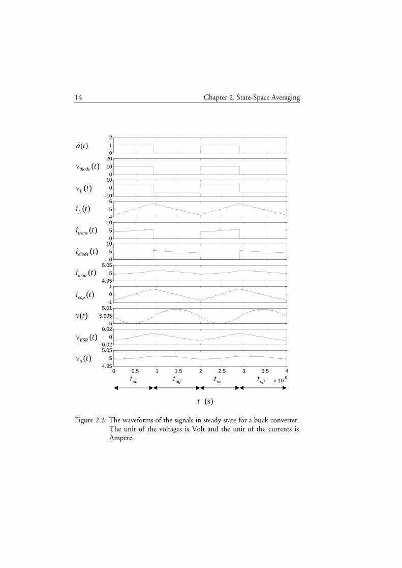
The components of a converter are not ideal and some of these non-idealities can be considered in a model. Only one non-ideality is considered in the model that will be used. The capacitor is modeled as an ideal capacitor in series with an ideal resistor with resistance cR . The resistance cR is called the Equivalent Series Resistance (ESR) of the capacitor. The ESR is used to represent all the power losses in the capacitor. The dependency of power loss on frequency is not addressed here. Figure 2.1 shows the circuit that will be used for the buck converter.
We assume that steady state is reached. The control signal, )(tδ , then consists of pulses with constant width. The waveforms of the signals in the circuit are as shown in Figure 2.2. In Section 2.4, a simulation model will be presented and this model is used to obtain the presented waveforms. The time intervals where the control signal )(tδ is high are called ont and the once where )(tδ is low are called offt . The switching period, sT , is the time between two successive positive flanks of )(tδ and hence equal to the sum of
ont and offt . The ratio of ont to sT is called the duty cycle or the duty ratio and it is denoted by )(td . The duty cycle is constant in steady state. During
ont the transistor operates in the on state and during offt the transistor operates in the off state. The voltage across the diode, )(tvdiode , is equal to the input voltage, )(tvg , during ont . The input voltage is held constant in the simulation. During offt the diode voltage is equal to zero since we assume that the converter is operated in continuous conduction mode (see Section 1.3). The diode voltage is filtered by the output low-pass LC-filter. The corner frequency of this filter is chosen to be much lower than the switching

Chapter 2. State-Space Averaging 13
Figure 2.1: The circuit of the buck converter.
frequency to obtain small magnitude of the ripple in the output voltage, )(tvo . Consequently, this voltage is approximately equal to the mean value of
the diode voltage. The mean value of )(tvdiode is lower than )(tvg . Therefore, )(tvo is lower than )(tvg in steady state.
The voltage across the inductor, )(tvL , is equal to the difference between )(tvdiode and )(tvo . The inductor current, )(tiL , is proportional to the
integral of )(tvL . Therefore, )(tiL increases during ont and decreases during
offt . During each time interval, the slope of )(tiL is almost constant since )(tvL is almost constant.
The inductor current is equal to the sum of the transistor current, )(titrans , and the diode current, )(tidiode . The transistor current is equal to
)(tiL during ont since )(tidiode is zero. The diode current is equal to )(tiL during offt since )(titrans is zero. The load current, )(tiload , is almost constant since )(tvo is almost constant. The capacitor current, )(ticap , is equal to the difference between )(tiL and )(tiload . The mean value of
)(ticap is zero in steady state. Consequently, )(tiload and )(tiL have the same mean value.
The voltage across the (ideal) capacitor, )(tv , is proportional to the integral of )(ticap . The voltage across the capacitor’s ESR, )(tvESR , is proportional to )(ticap . The output voltage, )(tvo , is equal to the sum of
)(tv and )(tvESR . Table 2.1 shows the parameter values used in the simulation. These are
also used by Ridley (1991). The switching frequency, sf , is equal to 50 kHz (the inverse of sT ). If the ESR in the capacitor is negligible, the corner frequency of the LC filter is
vg(t)
iL(t) L
vo(t)
C
Driver R
δ (t)
iload(t) itrans(t)
icap(t) idiode(t)
vdiode(t)
vL(t)
v(t)
vESR(t) Rc
14 Chapter 2. State-Space Averaging
0
1
2
0
10
20
-10
0
10
4
5
6
0
5
10
0
5
10
4.95
5
5.05
-1
0
1
5
5.005
5.01
-0.02
0
0.02
0 0.5 1 1.5 2 2.5 3 3.5 4
x 10-5
4.95
5
5.05
)(tδ
)(tvdiode
)(tvL
)(tiL
)(titrans
)(tidiode
)(tiload
)(ticap
)(tv
)(tvESR
)(tvo
ont offt ont offt
)s(t
Figure 2.2: The waveforms of the signals in steady state for a buck converter.
The unit of the voltages is Volt and the unit of the currents is Ampere.

Chapter 2. State-Space Averaging 15
kHz. 3.12
10 ==
LCf
π(2.1)
0f is thus much lower than sf , which means that the magnitude of the ripple in )(tvo is small. The magnitude is decreased if L , C , or sf is increased. However, there are disadvantages by doing so, for example: • If L is increased, it will take longer time for the inductor current to reach
a new average level. This is needed when a step change occurs in the load current.
• If L or C is increased, the volume, weight, and cost of the converter are increased.
• If sf is increased, the switching losses in the transistor are increased. The ESR of the capacitor also contributes to the ripple in )(tvo since this
voltage is equal to the sum of )(tv and )(tvESR . Furthermore, it causes a step change in )(tvo when a step change occurs in the load current. This is one of the reasons for the use of capacitors with low ESR in converters.
Table 2.1: The parameter values used in the simulation of the buck converter.
Parameter Value
L 37.5 µH
C 400 µF
cR 14 mΩ
R 1 Ω
)(tvg 11 V
)(td 0.455
sT 20 µs
2.3 Model of the Buck Converter
In this section, a linear time-invariant model of the buck converter is derived by means of state-space averaging. The converter can be described as switching between different time-invariant systems and the state-space
16 Chapter 2. State-Space Averaging
description of each one of these systems is first derived. These state-space descriptions are used as a starting point in the method of state-space averaging. This method is presented and then applied to the buck converter. The result is a linear time-invariant model in state-space description. Finally, several transfer functions are extracted from this model.
State-Space Description for Each Time Interval
Since it is assumed that the converter is operated in continuous conduction mode, two different systems must be considered. The state-space description of each one of these two systems is derived in this subsection.
While the transistor is on, the voltage across the diode is equal to the input voltage. The circuit in Figure 2.3 can therefore be used as a model of the buck converter during ont . In the figure, a current source is added. It injects the current )(tiinj into the output stage of the converter. This current is an input signal and is needed to determine the output impedance.
From Figure 2.3, the following equations are obtained:
( ) ,)()(1)(
tvtvLdt
tdiog
L −= (2.2)
,)()(
)(1)(
−−= tiR
tvti
Cdt
tdvinj
oL (2.3)
.)()(
)()()(
−−+= tiR
tvtiRtvtv inj
oLco (2.4)
(2.4) is rearranged to:
( ),)()()()()( titiRtvtvR
Rtv injLco
co −+=+ (2.5)
( )
,1
)()()()(
RR
titiRtvtv
c
injLco +
−+= (2.6)
Chapter 2. State-Space Averaging 17
Figure 2.3: The circuit of the buck converter during ont .
.)()()()( tiRR
RRtv
RR
Rti
RR
RRtv inj
c
c
cL
c
co +
−+
++
= (2.7)
(2.7) is used to substitute )(tvo in (2.2) and (2.3):
( ) ( )
( ) ,)()(1
)()()(
tiLRR
RRtv
L
tvLRR
Rti
LRR
RR
dt
tdi
injc
cg
cL
c
cL
++
++
−+
−= (2.8)
( ) ( )
( ) .)(1
)(
)(1
)()(1)(
tiC
tiCRR
R
tvCRR
tiCRR
Rti
Cdt
tdv
injinjc
c
cL
c
cL
−+
++
−+
−= (2.9)
(2.9) is simplified:
( ) ( ) ( ) .)()(1
)()(
tiCRR
Rtv
CRRti
CRR
R
dt
tdvinj
ccL
c +−
+−
+= (2.10)
The circuit in Figure 2.3 is a second order system. Let )(tiL and )(tv be
chosen as the state variables. Regard )(tvg and )(tiinj as the input signals and )(tvo as the output signal. By using (2.8), (2.10), and (2.7), the following state-space system is obtained:
vg(t)
iL(t) L
vo(t)
C
R
v(t)
Rc
iinj(t)
18 Chapter 2. State-Space Averaging
+=
+=
)()()(
)()()(
ttt
ttdt
td
uExCy
uBxAx
11
11 (2.11)
where
,)(
)()(
=
tv
tit Lx (2.12)
,)(
)()(
=
ti
tvt
inj
gu (2.13)
,)()( tvt o=y (2.14)
( ) ( )
( ) ( ),
1
+−
+
+−
+−
=
CRRCRR
RLRR
R
LRR
RR
cc
cc
c
1A (2.15)
( )
( ),
0
1
+−
+=
CRR
RLRR
RR
L
c
c
c
1B (2.16)
,
++
=cc
c
RR
R
RR
RR1C (2.17)
.0
+
−=c
c
RR
RR1E (2.18)
While the transistor is off, the voltage across the diode is equal to zero.
The circuit in Figure 2.4 can therefore be used as a model of the buck converter during offt . The circuit in Figure 2.3 and Figure 2.4 are the same if
Chapter 2. State-Space Averaging 19
Figure 2.4: The circuit of the buck converter during offt .
)(tvg is zero. Therefore, a state-space model for the circuit in Figure 2.4 can
be obtained by setting all the coefficients for )(tvg to zero in (2.11):
+=
+=
)()()(
)()()(
ttt
ttdt
td
uExCy
uBxAx
22
22 , (2.19)
where
12 AA = , (2.20)
( )
( ),
0
0
+−
+=
CRR
RLRR
RR
c
c
c
2B (2.21)
12 CC = , (2.22)
12 EE = . (2.23)
The Method of State-Space Averaging
The converter behaves like switching between the two different linear time-invariant systems (2.11) and (2.19) during the switching period, so it looks like a time-variant system. State-space averaging will be used in the next
iL(t) L
vo(t)
C
R
v(t)
Rc
iinj(t)

20 Chapter 2. State-Space Averaging
subsection to approximate this time-variant system with a linear continuous-time time-invariant system. In this subsection, the method of state-space averaging is presented. The first step is calculating a nonlinear time-invariant system by means of averaging and the second step is linearizing this nonlinear system. The presentation is a little different compared to the traditional one.
The two linear systems are first averaged with respect to their duration in the switching period:
( )( ) ( )( )( )( ) ( )( )
−++−+=
−++−+=
)()(1)()()(1)()(
)()(1)()()(1)()(
ttdtdttdtdt
ttdtdttdtddt
td
uEExCCy
uBBxAAx
2121
2121 (2.24)
(2.24) is an approximation of the time-variant system and new variable
names should formally have been used. To limit the number of variable names, this is not made. The duty cycle, )(td , is an additional input signal in (2.24). A new input vector is therefore defined:
.)(
)()(
=
td
tt
uu' (2.25)
This is not made in traditional presentations of state-space averaging, where the control signal )(td is kept separate from the disturbance signals )(tvg and )(tiinj . However, in system theory, all control signals and disturbance signals are put in an input vector.
Since the duty cycle can be considered to be a discrete-time signal with sampling interval sT , one cannot expect the system in (2.24) to be valid for frequencies higher than half the switching frequency.
The system in (2.24) is a nonlinear time-invariant system. It is nonlinear since there are products of two input signals and it is time-invariant since all the coefficients are independent of time.
A nonlinear time-invariant system with state-vector )(tx , input vector )(tu' , and output vector )(ty , are written as
( )( )
=
=
)(),()(
)(),()(
ttgt
ttfdt
td
u'xy
u'xx
, (2.26)
Chapter 2. State-Space Averaging 21
A straight-forward linearization is applied, where we define the deviations from an operating point as follows:
,)(ˆ)( tt xXx += (2.27)
,)(ˆ)( tt 'uU'u' += (2.28)
.)(ˆ)( tt yYy += (2.29)
Capital letters denote the operating-point (dc, steady-state) values and the hat-symbol (^) denotes perturbation (ac) signals. Assume that the operating point is an equilibrium point, i.e.
( ) .0)(),(
)(
)(=
==
U'u'Xx
u'x
t
tttf
(2.30)
The operating point output values are
( ) .)(),(
)(
)(
U'u'Xx
u'xY
==
=
t
tttg
(2.31)
The following linearized (ac, small-signal) system can now be obtained
from (2.26) (Goodwin, Graebe and Salgado, 2001, Section 3.10):
+=
+=
)(ˆ)(ˆ)(ˆ
)(ˆ)(ˆ)(ˆ
ttt
ttdt
td
'uE'xC'y
'uB'xA'x
, (2.32)
where
,
)()(
U'u'Xxx
A'
==
∂∂=
tt
f (2.33)

22 Chapter 2. State-Space Averaging
,
)()(
U'u'Xxu'
B'
==
∂∂=
tt
f (2.34)
,
)()(
U'u'Xxx
C'
==
∂∂=
tt
g (2.35)
.
)()(
U'u'Xxu'
E'
==
∂∂=
tt
g (2.36)
(2.32) is an approximation of the nonlinear system and new variable names should formally have been used. To limit the number of variable names, this is not made.
(2.24) is a special case of (2.26). The equations (2.28) and (2.30)-(2.36) will now be rewritten for this special case. The following equation is obtained if (2.28) is applied to (2.25):
,)(ˆ)(ˆ
)(
)()(
+
=
=
td
t
Dtd
tt
uUuu' (2.37)
The following variables are now defined:
)(1)(' tdtd −= , (2.38)
DD −=1' . (2.39)
The variable )(' td is equal to the fraction of the time the transistor is off. 'D is the operating-point value of )(' td . (2.30) and (2.31) are rewritten by using (2.24):
+=+=
EUCXY
BUAX0 , (2.40)
where

Chapter 2. State-Space Averaging 23
,' 21 AAA DD += (2.41)
,' 21 BBB DD += (2.42)
,' 21 CCC DD += (2.43)
.' 21 EEE DD += (2.44)
(2.40) is rewritten:
( )
+−=−=
−
−
UEBCAY
BUAX1
1
. (2.45)
(2.33)-(2.36) are reformulated by using (2.24):
( )( ) ,)(1)(
)()(
)()(
AAAx
A'
U'u'Xx
21
U'u'Xx
=−+=
∂∂=
==
==
tt
tt
tdtdf
(2.46)
( ) ( ) ( )[ ]
( ) ( )[ ] ,
)()()(1)(
)()(
)()(
)()(
UBBXAAB
uBBxAABB
uu'B'
2121
U'u'Xx212121
U'u'Xx
U'u'Xx
−+−
=−+−−+
=
∂∂
∂∂=
∂∂=
==
==
==
tt
tt
tt
tttdtd
d
fff
(2.47)
( )( ) ,)(1)(
)()(
)()(
CCCx
C'
U'u'Xx
21
U'u'Xx
=−+=
∂∂=
==
==
tt
tt
tdtdg
(2.48)

24 Chapter 2. State-Space Averaging
( ) ( ) ( )[ ]
( ) ( )[ ] ,
)()()(1)(
)()(
)()(
)()(
UEEXCCE
uEExCCEE
uu'E'
2121
U'u'Xx212121
U'u'Xx
U'u'Xx
−+−
=−+−−+
=
∂∂
∂∂=
∂∂=
==
==
==
tt
tt
tt
tttdtd
d
ggg
(2.49)
(2.32) can now be rewritten:
+=
+=
)(ˆ)(ˆ)(ˆ
)(ˆ)(ˆ)(ˆ
ttt
ttdt
td
'uE'xCy
'uB'xAx
. (2.50)
B' and E' are defined as
[ ] ,dBBB'= (2.51)
[ ] ,dEEE'= (2.52)
where
( ) ( ) ,UBBXAAB 2121d −+−= (2.53)
( ) ( ) .UEEXCCE 2121d −+−= (2.54)
The results of state-space averaging method are the dc model (2.45) (or
(2.40)) and the ac model (2.50).
Applying State-Space Averaging
The method of state-space averaging is applied to the buck converter in this subsection. The approximation made in the linearization is also considered.
The following equations are obtained if (2.27)-(2.29) are applied to (2.12)-(2.14):

Chapter 2. State-Space Averaging 25
,)(ˆ
)(ˆ
)(
)()(
+
=
=
tv
ti
V
I
tv
tit LLLx (2.55)
,
)(ˆ)(ˆ)(ˆ
0
)(
)(
)(
)(ˆ)(ˆ
)(
)()(
+
=
=
+
=
=
td
ti
tv
D
V
td
ti
tv
td
t
Dtd
tt inj
gg
inj
guUuu' (2.56)
.)(ˆ)()( tvVtvt ooo +==y (2.57)
Note that the dc value of )(tiinj is set to zero in (2.56) so that only the load resistor determines the dc load current.
(2.41)-(2.44) can easily be expanded since 1'=+ DD :
( ) ( )
( ) ( ),
1
+−
+
+−
+−
=
CRRCRR
RLRR
R
LRR
RR
cc
cc
c
A (2.58)
( )
( ),
0
1
+−
+=
CRR
RLRR
RR
LD
c
c
c
B (2.59)
,
++
=cc
c
RR
R
RR
RRC (2.60)
.0
+
−=c
c
RR
RRE (2.61)
The dc equations will now be derived. The following equations are
obtained if (2.40) is expanded:
26 Chapter 2. State-Space Averaging
( ) ( ) ,0 gc
Lc
c VL
DV
LRR
RI
LRR
RR+
+−
+−= (2.62)
( ) ( ) ,1
0 VCRR
ICRR
R
cL
c +−
+= (2.63)
.VRR
RI
RR
RRV
cL
c
co +
++
= (2.64)
(2.63) is simplified to:
.LRIV = (2.65)
(2.65) is inserted into (2.64):
.VVRR
RV
RR
RV
cc
co =
++
+= (2.66)
(2.65) is inserted in (2.62):
( ) ( ) ,0 gcc
c DVVRR
RV
RR
R+
+−
+−= (2.67)
.DV
V
g
= (2.68)
The dc current to the capacitor is zero and the dc voltage across the capacitor’s ESR is zero. This explains the results in (2.65) and (2.66). Equation (2.68) shows the dc amplification of the buck converter. The voltage across the diode is equal to gV during the fraction D of the time and equal to zero otherwise. V (= oV ) is equal to the mean value of the voltage across the diode ( gDV ).
(2.53) and (2.54) are expanded and written on an explicit form:
Chapter 2. State-Space Averaging 27
,000
01
=
+=
LVL gU0XBd (2.69)
.0=+= 0U0XEd (2.70)
(2.51) and (2.52) are expanded:
( )
( ),
00
+−
+=
CRR
RL
V
LRR
RR
L
D
c
g
c
c
B' (2.71)
.00
+
−=c
c
RR
RRE' (2.72)
All the coefficient matrices in the ac model (2.50) are now available.
The approximation made in the linearization is now considered. The following equation is obtained from the nonlinear system (2.24):
( ) ( )
( ) .)()()(1
)()()(
tiLRR
RRtvtd
L
tvLRR
Rti
LRR
RR
dt
tdi
injc
cg
cL
c
cL
++
++
−+
−=(2.73)
(2.73) is rewritten by using (2.55) and (2.56):
( )( ) ( ) ( ) ( )
( )( ) ( ) .)(ˆ)(ˆ)(ˆ1
)(ˆ)(ˆ)(ˆ
tiLRR
RRtvVtdD
L
tvVLRR
RtiI
LRR
RR
dt
tiId
injc
cgg
cLL
c
cLL
++++
+++
−++
−=+
(2.74)
(2.74) is rewritten by using (2.62):
28 Chapter 2. State-Space Averaging
( ) ( )
( ) .)(ˆ)(ˆ)(ˆ1)(ˆ1
)(ˆ1
)(ˆ)(ˆ)(ˆ
tiLRR
RRtvtd
LtdV
LtvD
L
tvLRR
Rti
LRR
RR
dt
tid
injc
cggg
cL
c
cL
++++
++
−+
−=(2.75)
The following equation is obtained from the linearized system in (2.50):
( ) ( )
( ) .)(ˆ)(ˆ)(ˆ
)(ˆ)(ˆ)(ˆ
tdL
Vti
LRR
RRtv
L
D
tvLRR
Rti
LRR
RR
dt
tid
ginj
c
cg
cL
c
cL
++
+
++
−+
−=(2.76)
The difference between (2.75) and (2.76) is the term Ltvtd g )(ˆ)(ˆ , which is a scaled product of two perturbation signals. Thus, this product is neglected in the linearization.
Extracting the Transfer Functions
The control-to-output transfer function, the output impedance and the audio susceptibility will now be derived from the linearized system in (2.50). Assume that the state is zero initially. The Laplace transform of (2.50) is
+=+=
)(ˆ)(ˆ)(ˆ
)(ˆ)(ˆ)(ˆ
sss
ssss
'uE'xCy
'uB'xAx. (2.77)
To be spared from introducing new variable names, the Laplace transform of a signal is denoted by the same name as the signal, e.g. )()( svtvL = , even if this is not a formally correct notation.
(2.77) is rewritten:
( )
+=−= −
)(ˆ)(ˆ)(ˆ
)(ˆ)(ˆ 1
sss
sss
'uE'xCy
'uB'AIx. (2.78)
The first equation in (2.78) is expanded:
Chapter 2. State-Space Averaging 29
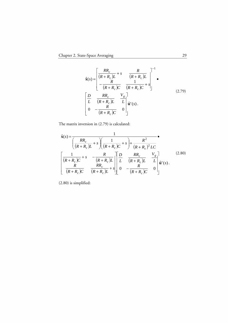
( ) ( )
( ) ( )
( )
( ).)(ˆ
00
1)(ˆ
1
s
CRR
RL
V
LRR
RR
L
D
sCRRCRR
RLRR
Rs
LRR
RR
s
c
g
c
c
cc
cc
c
'u
x
+−
+
•
+++
−
++
+=
−
(2.79)
The matrix inversion in (2.79) is calculated:
( ) ( ) ( )
( ) ( )
( ) ( )
( )
( ).)(ˆ
00
1
1
1)(ˆ
2
2
s
CRR
RL
V
LRR
RR
L
D
sLRR
RR
CRR
RLRR
Rs
CRR
LCRR
Rs
CRRs
LRR
RRs
c
g
c
c
c
c
c
cc
ccc
c
'u
x
+−
+
+++
+−+
+
•
++
+
+
+
+
=
(2.80)
(2.80) is simplified:
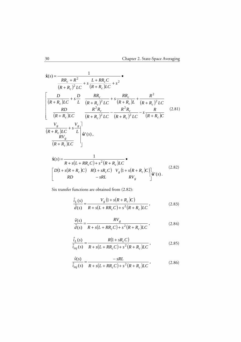
30 Chapter 2. State-Space Averaging
( ) ( )
( ) ( ) ( ) ( )
( ) ( ) ( ) ( )
( )
( )
,)(ˆ
1)(ˆ
2
2
2
2
2
2
2
22
2
s
LCRR
RVL
Vs
LCRR
V
CRR
Rs
LCRR
RR
LCRR
RR
LCRR
RD
LCRR
R
LRR
RRs
LCRR
RR
L
Ds
LCRR
D
sLCRR
CRRLs
LCRR
RRRs
c
g
g
c
g
cc
c
c
c
c
cc
c
c
c
c
c
c
c
c
'u
x
+
++
+−
+−
++
++
++
++
+
•+
++
++
+=
(2.81)
( ) ( )
( )( ) ( ) ( )( ).)(ˆ
111
1)(ˆ
2
sRVsRLRD
CRRsVCsRRCRRsD
LCRRsCRRLsRs
g
cgcc
cc
'u
x
−
+++++
•++++
=
(2.82)
Six transfer functions are obtained from (2.82):
( )( )
( ) ( ),
1
)(ˆ)(ˆ
2 LCRRsCRRLsR
CRRsV
sd
si
cc
cgL
++++
++= (2.83)
( ) ( ),
)(ˆ)(ˆ
2 LCRRsCRRLsR
RV
sd
sv
cc
g
++++= (2.84)
( )
( ) ( ),
1
)(ˆ)(ˆ
2 LCRRsCRRLsR
CsRR
si
si
cc
c
inj
L
+++++
= (2.85)
( ) ( ),
)(ˆ)(ˆ
2 LCRRsCRRLsR
sRL
si
sv
ccinj ++++−= (2.86)

Chapter 2. State-Space Averaging 31
( )( )
( ) ( ),
1
)(ˆ
)(ˆ2 LCRRsCRRLsR
CRRsD
sv
si
cc
c
g
L
++++++
= (2.87)
( ) ( ).
)(ˆ)(ˆ
2 LCRRsCRRLsR
RD
sv
sv
ccg ++++= (2.88)
The second equation in (2.78) is now expanded:
.)(ˆ00)(ˆ)(ˆ sRR
RRs
RR
R
RR
RRs
c
c
cc
c 'uxy
+
−+
++
= (2.89)
The control-to-output transfer function is obtained by combining (2.89), (2.83), and (2.84):
( )( )( ) ( ) ( )( )
( ) ( )( ) ( ) ( )( )
( )( ) ( )
.1
1
)(ˆ)(ˆ
)(ˆ)(ˆ
)(ˆ)(ˆ
2
2
2
2
LCRRsCRRLsR
CsRRV
LCRRsCRRLsRRR
CRRVsRRRRRV
LCRRsCRRLsRRR
VRCRRsVRR
sd
sv
RR
R
sd
si
RR
RR
sd
sv
cc
cg
ccc
cgccg
ccc
gcgc
c
L
c
co
++++
+
=+++++
+++
=+++++
+++
=+
++
=
(2.90)
The output impedance is obtained by combining (2.89), (2.85), and (2.86):
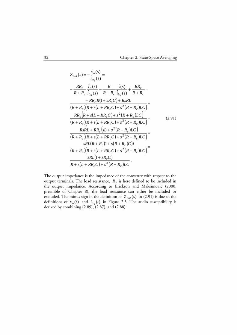
32 Chapter 2. State-Space Averaging
( )( ) ( ) ( )( )
( ) ( )( )( ) ( ) ( )( )
( )( )( ) ( ) ( )( )
( )( )( )( ) ( ) ( )( )
( )( ) ( )
.1
1
1
)(ˆ)(ˆ
)(ˆ)(ˆ
)(ˆ)(ˆ
)(
2
2
2
2
2
2
2
LCRRsCRRLsR
CsRsRL
LCRRsCRRLsRRR
CRRsRRsRL
LCRRsCRRLsRRR
LCRRssLRRRsRL
LCRRsCRRLsRRR
LCRRsCRRLsRRR
LCRRsCRRLsRRR
RsRLCsRRRR
RR
RR
si
sv
RR
R
si
si
RR
RR
si
svsZ
cc
c
ccc
cc
ccc
cc
ccc
ccc
ccc
cc
c
c
injcinj
L
c
c
inj
oout
+++++
=+++++
+++
=+++++
+++
=+++++
++++
++++++
++−
=+
++
−+
−
=−=
(2.91)
The output impedance is the impedance of the converter with respect to the output terminals. The load resistance, R , is here defined to be included in the output impedance. According to Erickson and Maksimovic (2000, preamble of Chapter 8), the load resistance can either be included or excluded. The minus sign in the definition of )(sZout in (2.91) is due to the definitions of )(tvo and )(tiinj in Figure 2.3. The audio susceptibility is derived by combining (2.89), (2.87), and (2.88):
Chapter 2. State-Space Averaging 33
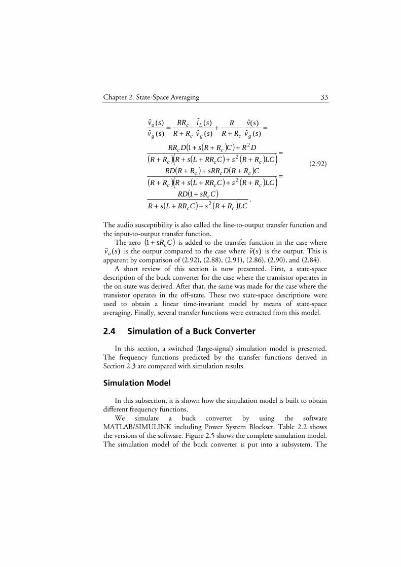
( )( )( ) ( ) ( )( )
( ) ( )( ) ( ) ( )( )
( )( ) ( )
.1
1
)(ˆ)(ˆ
)(ˆ
)(ˆ
)(ˆ
)(ˆ
2
2
2
2
LCRRsCRRLsR
CsRRD
LCRRsCRRLsRRR
CRRDsRRRRRD
LCRRsCRRLsRRR
DRCRRsDRR
sv
sv
RR
R
sv
si
RR
RR
sv
sv
cc
c
ccc
ccc
ccc
cc
gcg
L
c
c
g
o
+++++
=+++++
+++
=+++++
+++
=+
++
=
(2.92)
The audio susceptibility is also called the line-to-output transfer function and the input-to-output transfer function.
The zero ( )CsRc+1 is added to the transfer function in the case where )(ˆ svo is the output compared to the case where )(ˆ sv is the output. This is
apparent by comparison of (2.92), (2.88), (2.91), (2.86), (2.90), and (2.84). A short review of this section is now presented. First, a state-space
description of the buck converter for the case where the transistor operates in the on-state was derived. After that, the same was made for the case where the transistor operates in the off-state. These two state-space descriptions were used to obtain a linear time-invariant model by means of state-space averaging. Finally, several transfer functions were extracted from this model.
2.4 Simulation of a Buck Converter
In this section, a switched (large-signal) simulation model is presented. The frequency functions predicted by the transfer functions derived in Section 2.3 are compared with simulation results.
Simulation Model
In this subsection, it is shown how the simulation model is built to obtain different frequency functions.
We simulate a buck converter by using the software MATLAB/SIMULINK including Power System Blockset. Table 2.2 shows the versions of the software. Figure 2.5 shows the complete simulation model. The simulation model of the buck converter is put into a subsystem. The
34 Chapter 2. State-Space Averaging
subsystem has three input signals and three output signals and they are described in Table 2.3.
The subsystem is shown in Figure 2.6. The input and output signals are used as interface signals to the electrical part of the simulation model. The input signals vg and iinj, control a voltage and a current source, respectively. However, iinj is first multiplied by -1 to obtain a direction of the injected current that agrees with the one defined in Figure 2.3. The input signal delta, controls the transistor. A controllable switch emulates the diode. The inverse of delta is used to control this switch since the diode should conduct when the transistor in not conducting. To be able to start the simulation, a dummy resistor is included in the model. The resistance of this resistor is set to 1 MΩ and its effect on the simulation result is negligible. The output signals vo, iload, and iL are measurements of the output voltage, load current, and inductor current, respectively.
The input and output signals of the converter are connected as shown in Figure 2.5, to obtain the frequency functions of the converter. The input
Table 2.2: The versions of the software.
Software Version
MATLAB 5.3
SIMULINK 3.0
Power System Blockset 2.0
Table 2.3: The input and output signals of the subsystem.
Name Type Description
vg Input Input voltage, )(tvg
iinj Input Injected current, )(tiinj
delta Input Control signal, )(tδ
vo Output Output voltage, )(tvo
iload Output Load current, )(tiload
iL Output Inductor current, )(tiL

Chapter 2. State-Space Averaging 35
Figure 2.5: The complete simulation model.
Figure 2.6: The buck converter subsystem.
voltage, vg, is the sum of its dc value, Vg, and its ac value vghat. The injected current, iinj, and the duty cycle, d, are implemented in a corresponding way. The dc value of iinj, i.e. Iinj, is equal to zero in all the simulations. Only one signal generator at the time is activated. Specifying the amplitude to be equal to zero inactivates a signal generator.
The pulse width modulation (PWM) makes use of a saw-tooth signal. The signal sawtooth is increasing linearly from 0 to 1 as shown in Figure 2.7. When the signal reaches 1, it is instantly set to 0 again. The period of the signal is equal to sT , i.e. the switching period. When the signal sawtooth
Vg
S
R
Q
!Q
Iinj
signal
magnitude
angle
D
0.5
vg
iinj
delta
vo
iload
iL
Buck converter iinjhat
iL
iload
vo
iinj
vghat
vg
dhat
d
sawtooth
delta
3 iL
2 iload
1 vo
signal
-1
+ -
v 1 g
2 m
Transistor
Rdummy
Rc
R
NOT
L
signal +
-
+ i - + i
-
1 g
2 m Diode emulator
C
3 delta
2 iinj
1 vg
36 Chapter 2. State-Space Averaging
Figure 2.7: The waveforms of the signals in a pulse-width modulator.
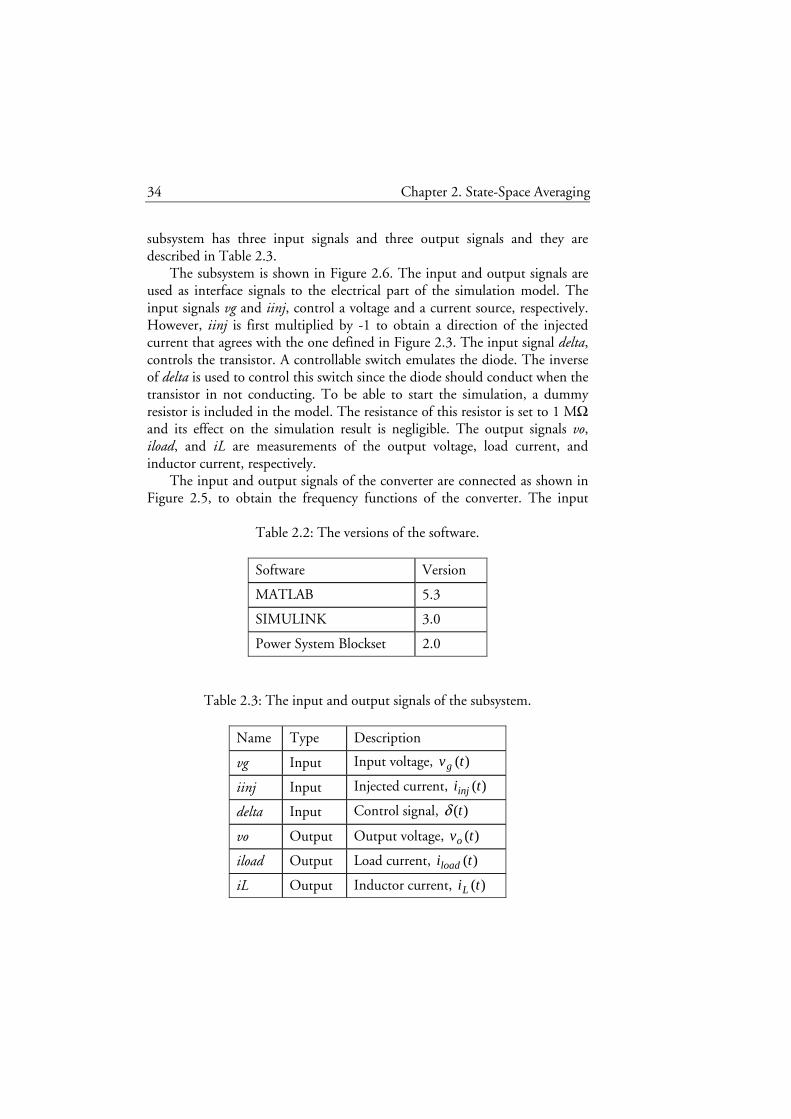
becomes greater than the duty cycle, d, the SR-latch is reset. A relay block is used to generate the reset signal. The output signal of the relay block is equal to 1 if the input signal is positive and equal to 0 if the input signal is negative. The hysteretic property in the relay block is thus not utilized. A pulse generator sets the SR-latch. The period of the set signal is equal to sT and the duration of each pulse is 1 percent of sT . The set signal is synchronized with the sawtooth signal so that the SR-latch is set each time the sawtooth signal goes from 1 to 0. The output signal of the SR-latch, delta, is a pulse train and the width of each pulse is determined by the duty cycle signal d. Note that it is possible to obtain PWM without using a SR-latch by using the inverse of the reset signal instead.
Consider the output signal vo of the converter which represents the output voltage. This signal has a Fourier component with a frequency equal to the frequency of the signal from the active signal generator. There exist other Fourier components in the output voltage (Erickson and Maksimovic, 2000, Section 7.1). The linearized model derived in Section 2.3 will be compared with the simulation results in the next subsection. The output of a linear system only consists of one Fourier component if the input is a
0 0.2 0.4 0.6 0.8 1 1.2 1.4 1.6 1.8 2
x 10-4
0
0.2
0.4
0.6
0.8
1
t (s)
saw
toot
h, d
0 0.2 0.4 0.6 0.8 1 1.2 1.4 1.6 1.8
x 10-4
0
0.2
0.4
0.6
0.8
1
t (s)
delta

Chapter 2. State-Space Averaging 37
sinusoidal. The frequency of this component is the same as the frequency of the input sinusoidal. To be able to compare the simulation results with the linearized model, only the Fourier component in the output voltage with a frequency equal to the frequency of the signal from the active signal generator is considered. A network analyzer also just considers this Fourier component (Erickson and Maksimovic, 2000, Section 8.5).
A Fourier component of a continuous-time periodic signal with period T is calculated by solving an integral where the length of the integration interval is equal to T (or a multiple of T ). Therefore, the period of the output voltage is now considered and let it be denoted by T . If none of the signal generator is active, then T is equal to the switching period sT . If one signal generator is active and the period of its signal is equal to sT , then T is still equal to sT . If the period of the signal from the signal generator is sT2 , then T = sT2 , and so forth. However, if the period of the signal from the signal generator is sT5.1 , then T is equal to sT3 , not sT5.1 . The relative difference between the periods of the two signals can be large if the period of the signal from the signal generator is chosen “badly”. In a simulation, the Fourier integral is solved numerically and the length of the integration interval is equal to T to obtain fast simulation. Furthermore, the period of the signal from the active signal generator should be equal to a multiple of the switching period sT , to avoid unnecessary large T . We follow these recommendations in all the simulations where the frequency functions of the converter is searched.
The switching frequency, sf , is equal to 50 kHz (the inverse of sT ). We evaluate the frequency functions at the frequencies 16666.6667 Hz ( 3sf≈ ), 10000 Hz ( 5sf= ), 5000 Hz, 2500 Hz, 1000 Hz, 500 Hz, 250 Hz, 100 Hz, and 50 Hz. To evaluate a frequency function at a specific frequency, the active signal generator is set to generate a sinusoidal with this frequency. The specific frequency is also set in the Fourier analysis block. This block has the output voltage vo as the input signal. It analyzes the Fourier component with the specific frequency by using a part of the signal vo. The part has an interval length equal to the inverse of the specific frequency. The interval length is equal to the period of the signal vo for each evaluated frequency and the Fourier component is therefore calculated correctly according to the previous discussion.
The result of the Fourier analysis is the magnitude and the phase of the component. The analysis is repeated during the simulation and the results are viewed by using the oscilloscope block. At the start of each simulation, the result of the Fourier analysis changes considerably since the inductor current

38 Chapter 2. State-Space Averaging
and the capacitor voltage are far from the final dc values. The simulation is stopped when the changes in the result of the Fourier analysis is negligible.
The result of a frequency function at a specific frequency is a magnitude and the phase. The magnitude is equal to the ratio of the magnitude of the output voltage, obtained from the Fourier analysis, to the magnitude of the signal from the active signal generator. The phase is equal to the phase of the output voltage, obtained from the Fourier analysis, since the phase of the signal from the active signal generator is zero.
The magnitude of the signal from the active signal generator should be small to avoid nonlinear properties of the converter. However, it should not be too small since this can result in numerical problems in the simulator. To obtain confidence that a suitable magnitude is chosen, we conduct an extra simulation with another magnitude. The magnitude is changed by least a factor of 2. If the change of the result of the frequency function at the specific frequency is negligible, the originally chosen magnitude is considered suitable.
A suitable solver algorithm and a small step size must be used in the simulation to obtain accurate results. We use the settings shown in Table 2.4 for the simulator solver. To obtain confidence that these settings are suitable, extra simulations have been conducted with other settings. The “Max step size” and the “Relative tolerance” have been reduced to one tenth of their values in the table but the change in the simulation result where negligible.
For each one of the frequencies mentioned previously, we conduct a simulation. This procedure is repeated three times since there are three different signal generators.
The parameter values shown in Table 2.1 are used in all the simulations except for )(tvg and )(td . They are of course not constant in the simulations. The values in the table are instead their dc values.
Table 2.4: The settings for the simulator solver.
Name Value
Type Variable-step, ode23tb (stiff/TR-BDF2)
Max step size 2e-7
Relative tolerance 1e-3
Initial step size auto
Absolute tolerance auto
Chapter 2. State-Space Averaging 39
Simulation Results
In this subsection, the frequency functions predicted by the transfer functions derived in Section 2.3 are compared with simulation results.
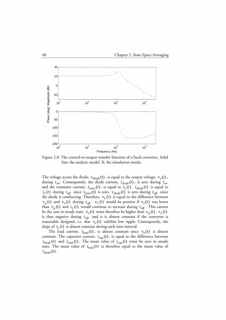
Figure 2.8 shows the Bode plot for the control-to-output transfer function (2.90). The frequency function obtained in the case where the magnitude of the signal dhat is non-zero in the simulations is also shown in the figure. The figure shows that the control-to-output transfer function derived in Section 2.3 agrees closely with the simulation results.
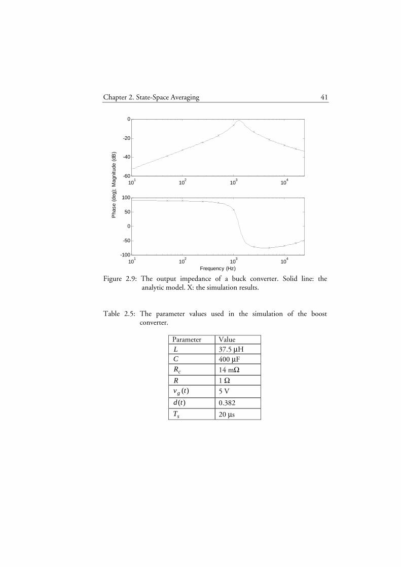
Figure 2.9 shows the Bode plot for the output impedance (2.91). The frequency function obtained in the case where the magnitude of the signal iinjhat is non-zero in the simulations is also shown in the figure. However, the phase of the frequency function is shifted 180 degrees due to the definition of the output impedance in (2.91). The figure shows that the output impedance derived in Section 2.3 agrees closely with the simulation results.
Figure 2.10 shows the Bode plot for the audio susceptibility (2.92). The frequency function obtained in the case where the magnitude of the signal vghat is non-zero in the simulations is also shown in the figure. The figure shows that the audio susceptibility derived in Section 2.3 agrees closely with the simulation results.
2.5 Operation of the Boost Converter
In this section, the circuit and operation of the boost converter are presented. A linear model of the boost converter will be derived in Section 2.6 and compared with simulation results in Section 2.7. The boost converter will be treated similarly as the buck converter in the previous sections.
Figure 2.11 shows the circuit that will be used for the boost converter. Figure 2.12 shows the waveforms of the signals in the circuit in steady state. We obtained the waveforms by using the simulation model that will be presented in Section 2.7. Table 2.5 shows the parameter values used in the simulation. The control signal, )(tδ , contains pulses with constant width in steady state. The transistor is on during ont and off during offt . The voltage across the inductor, )(tvL , is equal to the input voltage, )(tvg , during ont .
)(tvg is held constant in the simulation. The inductor current, )(tiL , is proportional to the integral of )(tvL . Therefore, )(tiL increases during ont .
40 Chapter 2. State-Space Averaging
Figure 2.8: The control-to-output transfer function of a buck converter. Solid line: the analytic model. X: the simulation results.
The voltage across the diode, )(tvdiode , is equal to the output voltage, )(tvo , during ont . Consequently, the diode current, )(tidiode , is zero during ont and the transistor current, )(titrans , is equal to )(tiL . )(tidiode is equal to
)(tiL during offt since )(titrans is zero. )(tvdiode is zero during offt since the diode is conducting. Therefore, )(tvL is equal to the difference between
)(tvg and )(tvo during offt . )(tvL would be positive if )(tvo was lower than )(tvg and )(tiL would continue to increase during offt . This cannot be the case in steady state. )(tvo must therefore be higher than )(tvg . )(tvL is thus negative during offt and it is almost constant if the converter is reasonable designed, i.e. that )(tvo exhibits low ripple. Consequently, the slope of )(tiL is almost constant during each time interval.
The load current, )(tiload , is almost constant since )(tvo is almost constant. The capacitor current, )(ticap , is equal to the difference between
)(tidiode and )(tiload . The mean value of )(ticap must be zero in steady state. The mean value of )(tiload is therefore equal to the mean value of
)(tidiode .
101
102
103
104
-20
0
20
40
101
102
103
104
-200
-150
-100
-50
0
Frequency (Hz)
Pha
se (
deg)
; M
agni
tude
(dB
)
Chapter 2. State-Space Averaging 41
Figure 2.9: The output impedance of a buck converter. Solid line: the analytic model. X: the simulation results.
Table 2.5: The parameter values used in the simulation of the boost converter.
Parameter Value L 37.5 µH C 400 µF
cR 14 mΩ
R 1 Ω )(tvg 5 V
)(td 0.382
sT 20 µs
101
102
103
104
-60
-40
-20
0
101
102
103
104
-100
-50
0
50
100
Frequency (Hz)
Pha
se (
deg)
; M
agni
tude
(dB
)

42 Chapter 2. State-Space Averaging
Figure 2.10: The audio susceptibility of a buck converter. Solid line: the analytic model. X: the simulation results.
Figure 2.11: The circuit of the boost converter.
101
102
103
104
-60
-40
-20
0
101
102
103
104
-200
-150
-100
-50
0
Frequency (Hz)
Pha
se (
deg)
; M
agni
tude
(dB
)
vg(t)
iL(t) L
vo(t)
C
R
δ (t)
iload(t)
icap(t)
idiode(t)
vL(t)
v(t)
vESR(t) Rc
Driver itrans(t)
vdiode(t)

Chapter 2. State-Space Averaging 43
0
1
2
-5
0
5
12
13
14
0
5
10
0
10
20
0
10
20
7.5
8
8.5
-10
0
10
7.9
8
8.1
-0.2
0
0.2
0 0.5 1 1.5 2 2.5 3 3.5 4
x 10-5
7.5
8
8.5
)(tδ )(tvL
)(tiL
)(tvdiode
)(tidiode
)(titrans
)(tiload
)(ticap
)(tv
)(tvESR
)(tvo
ont offt ont offt
)s(t
Figure 2.12: The waveforms of the signals in steady state for a boost
converter. The unit of the voltages is Volt and the unit of the currents is Ampere.
44 Chapter 2. State-Space Averaging
The voltage across the (ideal) capacitor, )(tv , is proportional to the integral of )(ticap . The voltage across the capacitor’s ESR, )(tvESR , is proportional to )(ticap . The output voltage, )(tvo , is equal to the sum of
)(tv and )(tvESR . The capacitor and the load are fed by )(tidiode . )(tidiode is discontinuous
and the magnitude of its ripple is high. Therefore, )(tvo is also discontinuous (due to the capacitor’s ESR). This is not the case for the buck converter where the capacitor and the load are fed by the inductor current. The inductor current is continuous and it is possible to keep the magnitude of its ripple at a reasonable level. It is therefore more difficult to obtain a low magnitude of the ripple in )(tvo for the boost converter than for the buck converter.
2.6 Model of the Boost Converter
A linear time-invariant model of the boost converter is derived by means of state-space averaging in this section. The methodology is analogous to the buck converter modeling.
State-Space Description for Each Time Interval
In this subsection, state-space descriptions of the boost converter are derived for the cases where the transistor operates in the on-state and in the off-state.
While the transistor is on, the voltage across the transistor is zero and the diode is not conducting. The circuit in Figure 2.13 can be used as a model of the boost converter during ont . In the figure, a current source is added.
From Figure 2.13, the following equations are obtained:
,)(1)(
tvLdt
tdig
L = (2.93)
,)()(1)(
−−= tiR
tv
Cdt
tdvinj
o (2.94)
.)()(
)()(
−−+= tiR
tvRtvtv inj
oco (2.95)
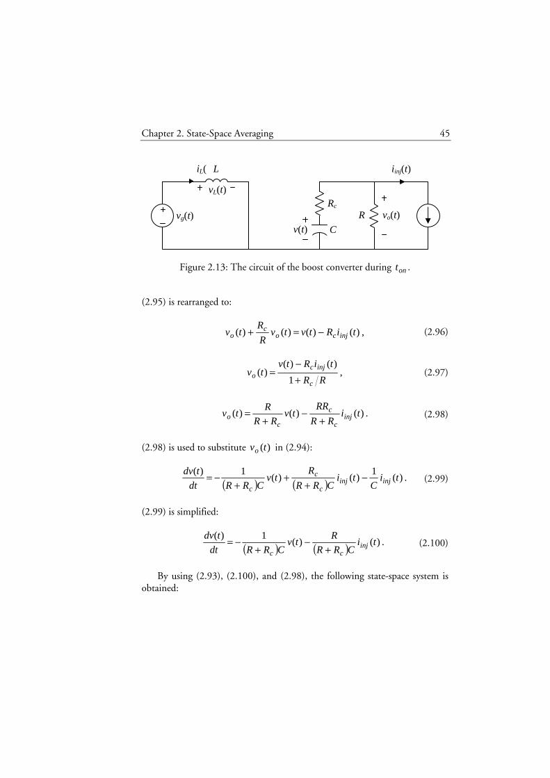
Chapter 2. State-Space Averaging 45
Figure 2.13: The circuit of the boost converter during ont .
(2.95) is rearranged to:
,)()()()( tiRtvtvR
Rtv injco
co −=+ (2.96)
,1
)()()(
RR
tiRtvtv
c
injco +
−= (2.97)
.)()()( tiRR
RRtv
RR
Rtv inj
c
c
co +
−+
= (2.98)
(2.98) is used to substitute )(tvo in (2.94):
( ) ( ) .)(1
)()(1)(
tiC
tiCRR
Rtv
CRRdt
tdvinjinj
c
c
c
−+
++
−= (2.99)
(2.99) is simplified:
( ) ( ) .)()(1)(
tiCRR
Rtv
CRRdt
tdvinj
cc +−
+−= (2.100)
By using (2.93), (2.100), and (2.98), the following state-space system is
obtained:
iL(
)
vg(t)
L
vo(t)
C
R
iinj(t)
vL(t)
v(t)
Rc
46 Chapter 2. State-Space Averaging
+=
+=
)()()(
)()()(
ttt
ttdt
td
uExCy
uBxAx
11
11 (2.101)
where
,)(
)()(
=
tv
tit Lx (2.102)
,)(
)()(
=
ti
tvt
inj
gu (2.103)
,)()( tvt o=y (2.104)
( )
,10
00
+−=
CRR c
1A (2.105)
( ),
0
01
+−
=
CRR
RL
c
1B (2.106)
,0
+
=cRR
R1C (2.107)
.0
+
−=c
c
RR
RR1E (2.108)
While the transistor is off, the voltage across the diode is equal to zero.
The circuit in Figure 2.3 can therefore be used as a model of the boost converter during offt . A state-space model for this circuit is presented in Section 2.3, (2.11)-(2.18). The state-space model of the boost converter during offt is thus

Chapter 2. State-Space Averaging 47
+=
+=
)()()(
)()()(
ttt
ttdt
td
uExCy
uBxAx
22
22 , (2.109)
where
( ) ( )
( ) ( ),
1
+−
+
+−
+−
=
CRRCRR
RLRR
R
LRR
RR
cc
cc
c
2A (2.110)
( )
( ),
0
1
+−
+=
CRR
RLRR
RR
L
c
c
c
2B (2.111)
,
++
=cc
c
RR
R
RR
RR2C (2.112)
.0 12 EE =
+
−=c
c
RR
RR (2.113)
Applying State-Space Averaging
The method of state-space averaging is applied to the boost converter in this subsection.
The following equations are obtained if (2.41)-(2.44) are expanded:
( ) ( )
( ) ( ),
1'
''
+−
+
+−
+−
=
CRRCRR
RD
LRR
RD
LRR
RRD
cc
cc
c
A (2.114)
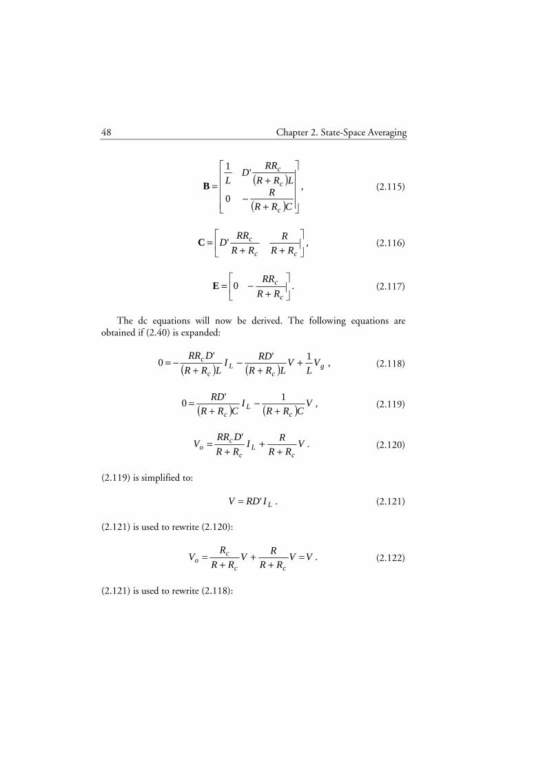
48 Chapter 2. State-Space Averaging
( )
( ),
0
'1
+−
+=
CRR
RLRR
RRD
L
c
c
c
B (2.115)
,'
++
=cc
c
RR
R
RR
RRDC (2.116)
.0
+
−=c
c
RR
RRE (2.117)
The dc equations will now be derived. The following equations are
obtained if (2.40) is expanded:
( ) ( ) ,1''
0 gc
Lc
c VL
VLRR
RDI
LRR
DRR+
+−
+−= (2.118)
( ) ( ) ,1'
0 VCRR
ICRR
RD
cL
c +−
+= (2.119)
.'
VRR
RI
RR
DRRV
cL
c
co +
++
= (2.120)
(2.119) is simplified to:
.' LIRDV = (2.121)
(2.121) is used to rewrite (2.120):
.VVRR
RV
RR
RV
cc
co =
++
+= (2.122)
(2.121) is used to rewrite (2.118):
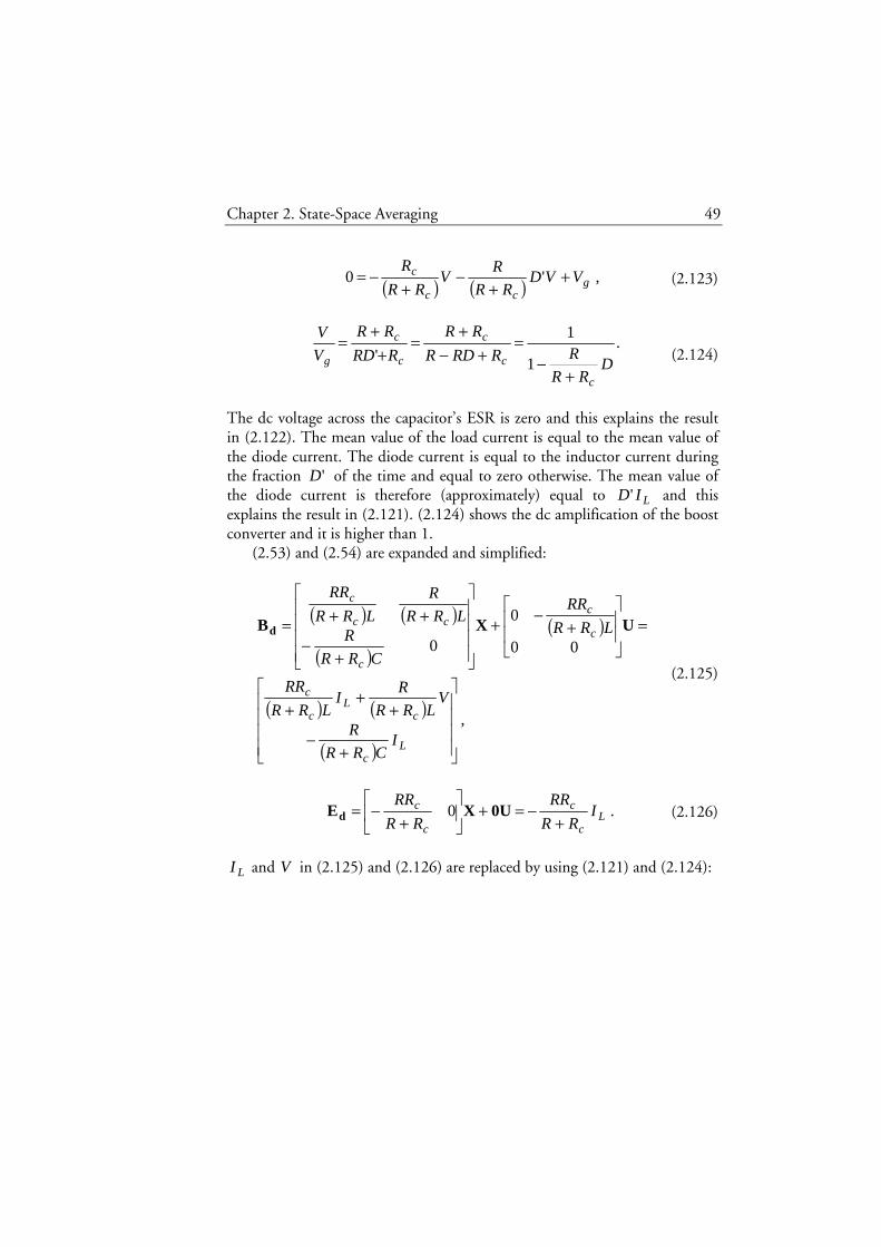
Chapter 2. State-Space Averaging 49
( ) ( ) ,'0 gcc
c VVDRR
RV
RR
R+
+−
+−= (2.123)
.
1
1
' DRR
RRRDR
RR
RRD
RR
V
V
c
c
c
c
c
g
+−
=+−
+=
++
= (2.124)
The dc voltage across the capacitor’s ESR is zero and this explains the result in (2.122). The mean value of the load current is equal to the mean value of the diode current. The diode current is equal to the inductor current during the fraction 'D of the time and equal to zero otherwise. The mean value of the diode current is therefore (approximately) equal to LID' and this explains the result in (2.121). (2.124) shows the dc amplification of the boost converter and it is higher than 1.
(2.53) and (2.54) are expanded and simplified:
( ) ( )
( )( )
( ) ( )
( ),
00
0
0
+−
++
+
=
+
−+
+−
++=
Lc
cL
c
c
c
c
c
cc
c
ICRR
R
VLRR
RI
LRR
RR
LRR
RR
CRR
RLRR
R
LRR
RR
UXBd
(2.125)
.0 Lc
c
c
c IRR
RR
RR
RR
+−=+
+
−= 0UXEd (2.126)
LI and V in (2.125) and (2.126) are replaced by using (2.121) and (2.124):

50 Chapter 2. State-Space Averaging
( ) ( )
( )
( )( )
( )
( ),
''
'
'
'
'
'
1'
'
'
+−
=
+−
++
=
+−
++
+=
CDRRD
VLD
V
CDRR
VLDRR
VRRD
VCDRR
VLDRR
RDV
LDRR
R
c
g
g
c
c
c
c
cc
c
dB
(2.127)
( ) ( ) .''' DRRD
VRV
DRR
R
c
gc
c
c
+−=
+−=dE (2.128)
(2.51) and (2.52) are expanded:
( )
( ) ( )
,
''0
'
'1
+−
+−
+=
CDRRD
V
CRR
R
LD
V
LRR
DRR
L
c
g
c
g
c
c
B' (2.129)
( ) .''
0
+−
+−=
c
gc
c
c
RRDD
VR
RR
RRE' (2.130)
All the coefficient matrices in the ac model (2.50) are now available.
Extracting the Transfer Functions
The control-to-output transfer function, the output impedance and the audio susceptibility will now be extracted from the linearized system. The first equation in (2.78) is written on the form:

Chapter 2. State-Space Averaging 51
( ) ( )
( ) ( )
( )
( ) ( )
.)(ˆ
''0
'
'1
1'
''
)(ˆ
1
s
CDRRD
V
CRR
R
LD
V
LRR
DRR
L
sCRRCRR
RDLRR
RDs
LRR
DRR
s
c
g
c
g
c
c
cc
cc
c
'u
x
+−
+−
+
•
+++
−
++
+=
−
(2.131)
The matrix inversion in (2.131) is calculated:
( ) ( ) ( )
( ) ( )
( ) ( )
( )
( ) ( )
.)(ˆ
''0
'
'1
''
'1
'1'
1)(ˆ
2
22
s
CDRRD
V
CRR
R
LD
V
LRR
DRR
L
sLRR
DRR
CRR
RDLRR
RDs
CRR
LCRR
DRs
CRRs
LRR
DRRs
c
g
c
g
c
c
c
c
c
cc
ccc
c
'u
x
+−
+−
+
•
+++
+−+
+
•
++
+
+
+
+
=
(2.132)
(2.132) is modified to:

52 Chapter 2. State-Space Averaging
( ) ( )
( ) ( ) ( ) ( )
( ) ( ) ( ) ( )
( ) ( )( )
( ) ( )( ) ( )
,)(ˆ
''''
'''
'
''
'''
'''11
'''
1)(ˆ
2
2
2
22
2
2
2
22
22
s
CDRRD
Vs
LCDRRDRR
VDRR
LCRR
RVLCDRRDRR
VRD
LD
Vs
LCDRR
V
CRR
Rs
LCRR
DRR
LCRR
DRR
LCRR
RD
LCRR
DR
LRR
DRRs
LCRR
DRR
Ls
LCRR
sLCRR
CDRRLs
LCRR
DRDRRs
c
g
cc
gc
c
g
cc
gg
c
g
cc
c
c
c
c
cc
c
c
c
c
c
c
c
c
'u
x
+−
++−
+
++++
+
+−
+−
++
++
++
++
+
•+
++
++
+=
(2.133)
( ) ( ) ( ) ( )( ) ( )
( )
( )
( ) ( )( ).)(ˆ
'''
'
'1
'
''
1'1
'''
1)(ˆ
22
2
2
s
LRRsDRRRDD
V
CRRsRRD
RD
D
V
sRLRR
DDRRRD
CsRRDCRRs
LCRRsCDRRLsRRRRDRDs
cc
g
cc
g
c
c
cc
cccc
'u
x
+−+
++
++
−+
−
+++
•++++++
=
(2.134)
Six transfer functions are derived from (2.134):
( )
( ) ( ) ( ) ( ),
'''
'
'1
'
)(ˆ)(ˆ
2 LCRRsCDRRLsRRRRDRD
CRRsRRD
RD
D
V
sd
si
cccc
cc
g
L
++++++
++
++
=
(2.135)
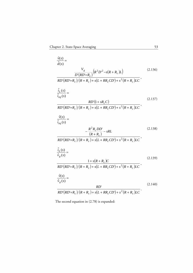
Chapter 2. State-Space Averaging 53
( ) ( )( )( ) ( ) ( ) ( )
,'''
'''
)(ˆ)(ˆ
2
22
LCRRsCDRRLsRRRRDRD
LRRsDRRRDD
V
sd
sv
cccc
cc
g
++++++
+−+
=
(2.136)
( )( ) ( ) ( ) ( )
,'''
1'
)(ˆ)(ˆ
2 LCRRsCDRRLsRRRRDRD
CsRRD
si
si
cccc
c
inj
L
+++++++
=
(2.137)
( )( ) ( ) ( ) ( )
,'''
'
)(ˆ)(ˆ
2
2
LCRRsCDRRLsRRRRDRD
sRLRR
DDRR
si
sv
cccc
c
c
inj
++++++
−+
−
=
(2.138)
( )( ) ( ) ( ) ( )
,'''
1
)(ˆ
)(ˆ
2 LCRRsCDRRLsRRRRDRD
CRRs
sv
si
cccc
c
g
L
++++++++
= (2.139)
( ) ( ) ( ) ( ).
'''
'
)(ˆ)(ˆ
2 LCRRsCDRRLsRRRRDRD
RD
sv
sv
cccc
g
++++++
=
(2.140)
The second equation in (2.78) is expanded:
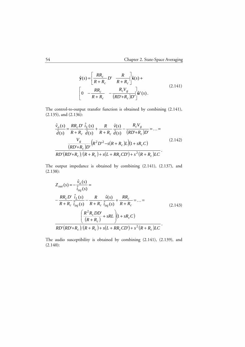
54 Chapter 2. State-Space Averaging
( ) .)(ˆ''
0
)(ˆ')(ˆ
sDRRD
VR
RR
RR
sRR
RD
RR
RRs
c
gc
c
c
cc
c
'u
xy
+−
+−
+
++
=
(2.141)
The control-to-output transfer function is obtained by combining (2.141), (2.135), and (2.136):
( )
( ) ( )( )( )
( ) ( ) ( ) ( ).
'''
1'''
'')(ˆ)(ˆ
)(ˆ)(ˆ'
)(ˆ)(ˆ
2
22
LCRRsCDRRLsRRRRDRD
CsRLRRsDRDRRD
V
DRRD
VR
sd
sv
RR
R
sd
si
RR
DRR
sd
sv
cccc
ccc
g
c
gc
c
L
c
co
++++++
++−+
==+
−+
++
= K
(2.142)
The output impedance is obtained by combining (2.141), (2.137), and (2.138):
( ) ( )
( ) ( ) ( ) ( ).
'''
1'
)(ˆ)(ˆ
)(ˆ)(ˆ'
)(ˆ)(ˆ
)(
2
2
LCRRsCDRRLsRRRRDRD
CsRsRLRR
DDRR
RR
RR
si
sv
RR
R
si
si
RR
DRR
si
svsZ
cccc
cc
c
c
c
injcinj
L
c
c
inj
oout
++++++
+
+
+
==+
++
−+
−
=−=
K(2.143)
The audio susceptibility is obtained by combining (2.141), (2.139), and (2.140):
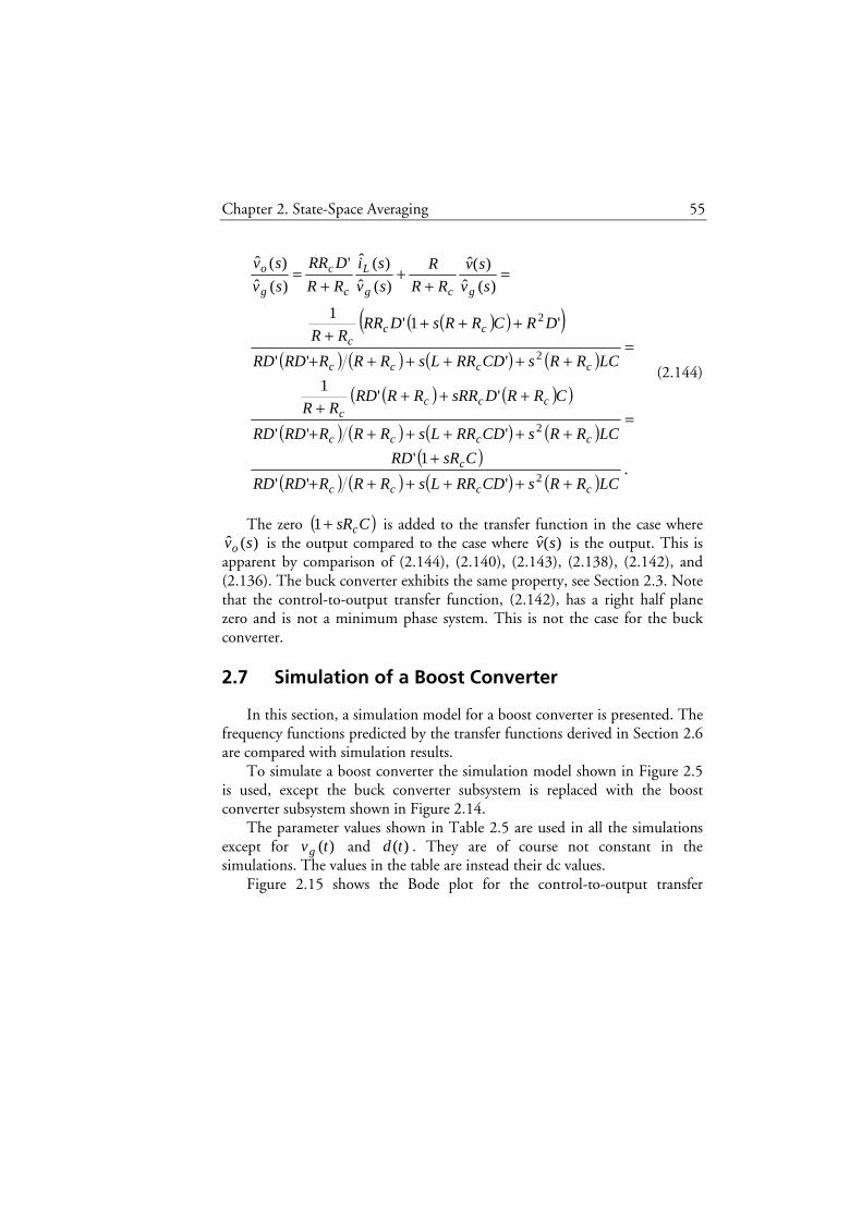
Chapter 2. State-Space Averaging 55
( )( )( )( ) ( ) ( ) ( )
( ) ( )( )
( ) ( ) ( ) ( )( )
( ) ( ) ( ) ( ).
'''
1'
'''
''1
'''
'1'1
)(ˆ)(ˆ
)(ˆ
)(ˆ'
)(ˆ
)(ˆ
2
2
2
2
LCRRsCDRRLsRRRRDRD
CsRRD
LCRRsCDRRLsRRRRDRD
CRRDsRRRRRDRR
LCRRsCDRRLsRRRRDRD
DRCRRsDRRRR
sv
sv
RR
R
sv
si
RR
DRR
sv
sv
cccc
c
cccc
cccc
cccc
ccc
gcg
L
c
c
g
o
+++++++
=++++++
++++
=++++++
++++
=+
++
=
(2.144)
The zero ( )CsRc+1 is added to the transfer function in the case where )(ˆ svo is the output compared to the case where )(ˆ sv is the output. This is
apparent by comparison of (2.144), (2.140), (2.143), (2.138), (2.142), and (2.136). The buck converter exhibits the same property, see Section 2.3. Note that the control-to-output transfer function, (2.142), has a right half plane zero and is not a minimum phase system. This is not the case for the buck converter.
2.7 Simulation of a Boost Converter
In this section, a simulation model for a boost converter is presented. The frequency functions predicted by the transfer functions derived in Section 2.6 are compared with simulation results.
To simulate a boost converter the simulation model shown in Figure 2.5 is used, except the buck converter subsystem is replaced with the boost converter subsystem shown in Figure 2.14.
The parameter values shown in Table 2.5 are used in all the simulations except for )(tvg and )(td . They are of course not constant in the simulations. The values in the table are instead their dc values.
Figure 2.15 shows the Bode plot for the control-to-output transfer
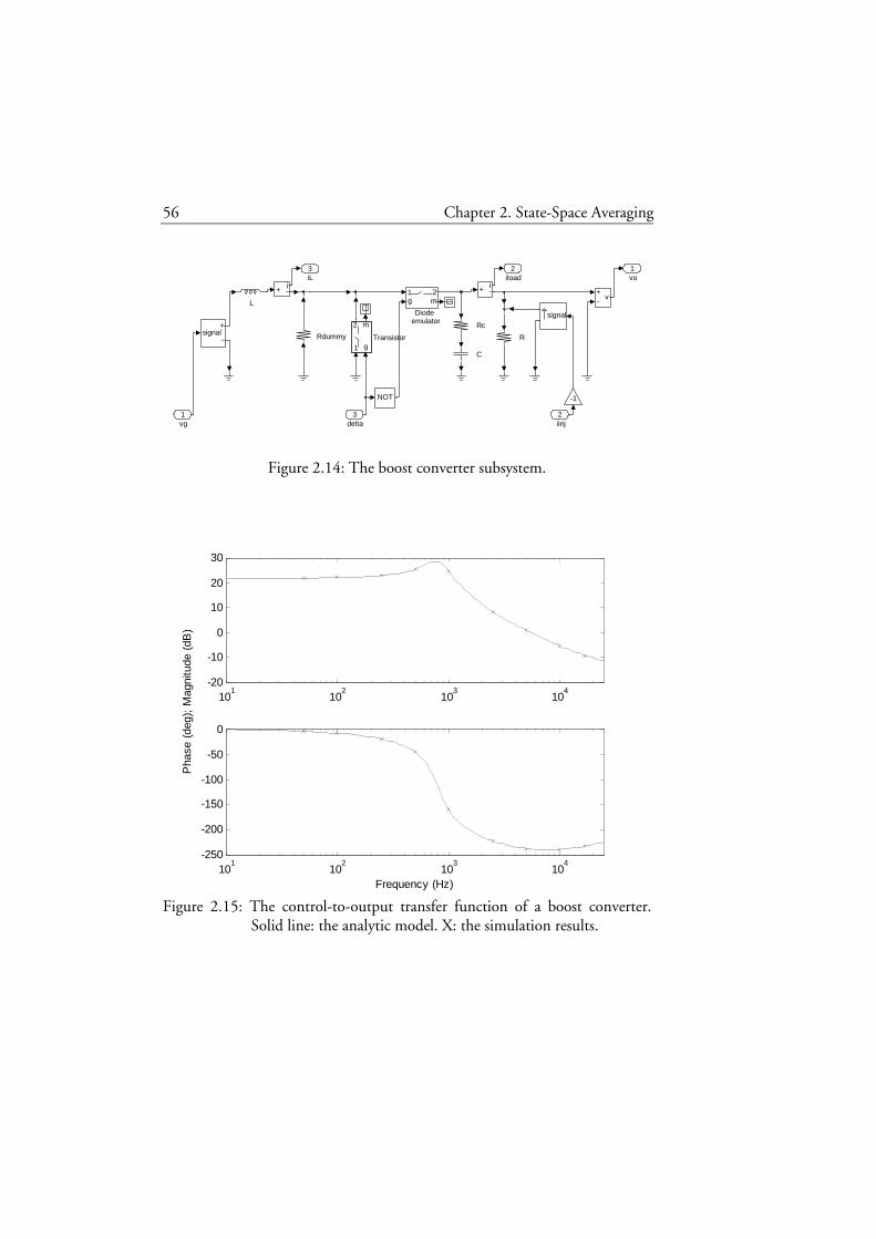
56 Chapter 2. State-Space Averaging
Figure 2.14: The boost converter subsystem.
Figure 2.15: The control-to-output transfer function of a boost converter. Solid line: the analytic model. X: the simulation results.
3 iL
2 iload
1 vo
signal
-1
+ - v
1 g
2 m
Transistor Rdummy
Rc
R
NOT
L
signal +
-
+ i - + i
- 1 g
2 m
Diode emulator
C
3 delta
2 iinj
1 vg
101
102
103
104
-20
-10
0
10
20
30
101
102
103
104
-250
-200
-150
-100
-50
0
Frequency (Hz)
Pha
se (
deg)
; M
agni
tude
(dB
)
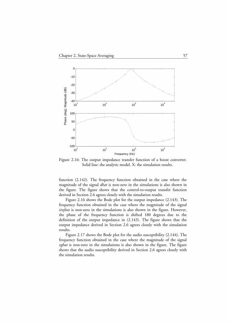
Chapter 2. State-Space Averaging 57
Figure 2.16: The output impedance transfer function of a boost converter. Solid line: the analytic model. X: the simulation results.
function (2.142). The frequency function obtained in the case where the magnitude of the signal dhat is non-zero in the simulations is also shown in the figure. The figure shows that the control-to-output transfer function derived in Section 2.6 agrees closely with the simulation results.
Figure 2.16 shows the Bode plot for the output impedance (2.143). The frequency function obtained in the case where the magnitude of the signal iinjhat is non-zero in the simulations is also shown in the figure. However, the phase of the frequency function is shifted 180 degrees due to the definition of the output impedance in (2.143). The figure shows that the output impedance derived in Section 2.6 agrees closely with the simulation results.
Figure 2.17 shows the Bode plot for the audio susceptibility (2.144). The frequency function obtained in the case where the magnitude of the signal vghat is non-zero in the simulations is also shown in the figure. The figure shows that the audio susceptibility derived in Section 2.6 agrees closely with the simulation results.
101
102
103
104
-40
-30
-20
-10
0
101
102
103
104
-100
-50
0
50
100
Frequency (Hz)
Pha
se (
deg)
; M
agni
tude
(dB
)
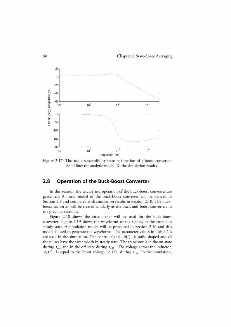
58 Chapter 2. State-Space Averaging
Figure 2.17: The audio susceptibility transfer function of a boost converter. Solid line: the analytic model. X: the simulation results.
2.8 Operation of the Buck-Boost Converter
In this section, the circuit and operation of the buck-boost converter are presented. A linear model of the buck-boost converter will be derived in Section 2.9 and compared with simulation results in Section 2.10. The buck-boost converter will be treated similarly as the buck and boost converters in the previous sections.
Figure 2.18 shows the circuit that will be used for the buck-boost converter. Figure 2.19 shows the waveforms of the signals in the circuit in steady state. A simulation model will be presented in Section 2.10 and this model is used to generate the waveforms. The parameter values in Table 2.6 are used in the simulation. The control signal, )(tδ , is pulse shaped and all the pulses have the same width in steady state. The transistor is in the on state during ont and in the off state during offt . The voltage across the inductor,
)(tvL , is equal to the input voltage, )(tvg , during ont . In the simulation,
101
102
103
104
-60
-40
-20
0
20
101
102
103
104
-200
-150
-100
-50
0
Frequency (Hz)
Pha
se (
deg)
; M
agni
tude
(dB
)
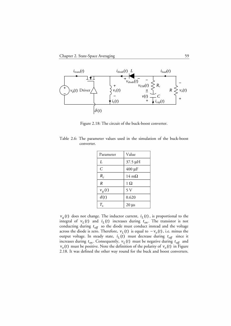
Chapter 2. State-Space Averaging 59
Figure 2.18: The circuit of the buck-boost converter.
Table 2.6: The parameter values used in the simulation of the buck-boost converter.
Parameter Value
L 37.5 µH
C 400 µF
cR 14 mΩ
R 1 Ω
)(tvg 5 V
)(td 0.620
sT 20 µs
)(tvg does not change. The inductor current, )(tiL , is proportional to the
integral of )(tvL and )(tiL increases during ont . The transistor is not conducting during offt so the diode must conduct instead and the voltage across the diode is zero. Therefore, )(tvL is equal to )(tvo− , i.e. minus the output voltage. In steady state, )(tiL must decrease during offt since it increases during ont . Consequently, )(tvL must be negative during offt and
)(tvo must be positive. Note the definition of the polarity of )(tvo in Figure 2.18. It was defined the other way round for the buck and boost converters.
idiode(t)
vg(t)
iL(t)
L
vo(t)
C
Driver R
δ (t)
iload(t) itrans(t)
icap(t)
vdiode(t)
vL(t)
v(t)
vESR(t) Rc
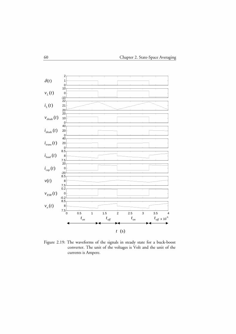
60 Chapter 2. State-Space Averaging
0
1
2
-10
0
10
20
21
22
0
10
20
0
20
40
0
20
40
7.5
8
8.5
-20
0
20
7.5
8
8.5
-0.2
0
0.2
0 0.5 1 1.5 2 2.5 3 3.5 4
x 10-5
7.5
8
8.5
)(tδ )(tvL
)(tiL
)(tvdiode
)(tidiode
)(titrans
)(tiload
)(ticap
)(tv
)(tvESR
)(tvo
ont offt ont offt
)s(t
Figure 2.19: The waveforms of the signals in steady state for a buck-boost
converter. The unit of the voltages is Volt and the unit of the currents is Ampere.

Chapter 2. State-Space Averaging 61
)(tvL is almost constant during offt if the converter is reasonable designed, i.e. that the magnitude of the ripple in )(tvo is low. Hence, during each time interval the slope of )(tiL is almost constant.
The voltage across the diode, )(tvdiode , is equal to )()( tvtv og + during
ont . The diode current, )(tidiode , is therefore zero during ont and the transistor current, )(titrans , is equal to )(tiL . )(tidiode is equal to )(tiL during offt since )(titrans is zero.
Since )(tvo is almost constant, also the load current, )(tiload , is almost constant. The capacitor current, )(ticap , is equal to the difference between
)(tidiode and )(tiload . In steady state, the mean value of )(ticap is zero and the mean value of )(tiload is therefore equal to the mean value of )(tidiode .
The voltage across the (ideal) capacitor, )(tv , is proportional to the integral of )(ticap . The voltage across the capacitor’s ESR, )(tvESR , is proportional to )(ticap . The output voltage, )(tvo , is equal to the sum of
)(tv and )(tvESR . The capacitor and the load are fed by )(tidiode which is the case also for
the boost converter. See Section 2.5 for a discussion about the consequences.
2.9 Model of the Buck-Boost Converter
A linear time-invariant model of the buck-boost converter is derived by means of state-space averaging in this section. The methodology is analogous to the modeling of the buck and boost converters.
State-Space Description for Each Time Interval
In this subsection, state-space descriptions of the buck-boost converter are derived for the cases where the transistor operates in the on-state and in the off-state.
While the transistor is on, the voltage across the transistor is zero and the diode is not conducting. The circuit in Figure 2.13 can therefore be used as a model of the buck-boost converter during ont . A consequence of using this circuit is that the injected current, )(tiinj , is defined in opposite direction compared to the definition used for the boost converter. This will be compensated for in the simulation model for the buck-boost converter. (Compare Figure 2.14 and Figure 2.20.) A state-space model for the circuit in Figure 2.13 is presented in Section 2.6, (2.101)-(2.108). The state-space model of the buck-boost converter during ont is thus

62 Chapter 2. State-Space Averaging
+=
+=
)()()(
)()()(
ttt
ttdt
td
uExCy
uBxAx
11
11 , (2.145)
where
,)(
)()(
=
tv
tit Lx (2.146)
,)(
)()(
=
ti
tvt
inj
gu (2.147)
,)()( tvt o=y (2.148)
( )
,10
00
+−=
CRR c
1A (2.149)
( ),
0
01
+−
=
CRR
RL
c
1B (2.150)
,0
+
=cRR
R1C (2.151)
.0
+
−=c
c
RR
RR1E (2.152)
While the transistor is off, the voltage across the diode is equal to zero.
The circuit in Figure 2.4 can therefore be used as a model of the buck-boost converter during offt . A state-space model for this circuit is presented in Section 2.3, (2.19)-(2.23). The state-space model of the buck-boost converter during offt is thus
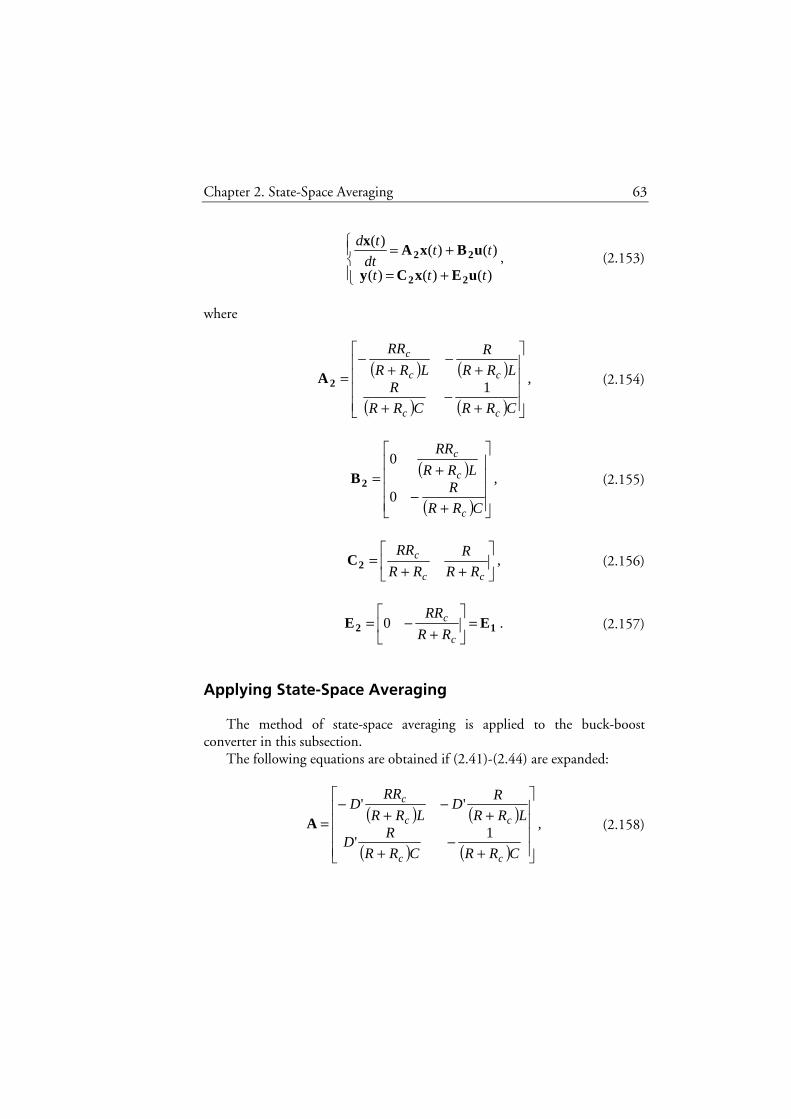
Chapter 2. State-Space Averaging 63
+=
+=
)()()(
)()()(
ttt
ttdt
td
uExCy
uBxAx
22
22 , (2.153)
where
( ) ( )
( ) ( ),
1
+−
+
+−
+−
=
CRRCRR
RLRR
R
LRR
RR
cc
cc
c
2A (2.154)
( )
( ),
0
0
+−
+=
CRR
RLRR
RR
c
c
c
2B (2.155)
,
++
=cc
c
RR
R
RR
RR2C (2.156)
.0 12 EE =
+
−=c
c
RR
RR (2.157)
Applying State-Space Averaging
The method of state-space averaging is applied to the buck-boost converter in this subsection.
The following equations are obtained if (2.41)-(2.44) are expanded:
( ) ( )
( ) ( ),
1'
''
+−
+
+−
+−
=
CRRCRR
RD
LRR
RD
LRR
RRD
cc
cc
c
A (2.158)

64 Chapter 2. State-Space Averaging
( )
( ),
0
'1
+−
+=
CRR
RLRR
RRD
LD
c
c
c
B (2.159)
,'
++
=cc
c
RR
R
RR
RRDC (2.160)
.0
+
−=c
c
RR
RRE (2.161)
The dc equations will now be derived. The following equations are
obtained if (2.40) is expanded:
( ) ( ) ,''
0 gc
Lc
c VL
DV
LRR
RDI
LRR
DRR+
+−
+−= (2.162)
( ) ( ) ,1'
0 VCRR
ICRR
RD
cL
c +−
+= (2.163)
.'
VRR
RI
RR
DRRV
cL
c
co +
++
= (2.164)
(2.163) is rewritten:
.' LIRDV = (2.165)
(2.165) is used to rewrite (2.164):
.VVRR
RV
RR
RV
cc
co =
++
+= (2.166)
(2.165) is used to rewrite (2.162):

Chapter 2. State-Space Averaging 65
,'0 gcc
c DVVDRR
RV
RR
R+
+−
+−= (2.167)
( ) ( ).
1' DRR
RD
RRDR
RRD
RRD
RRD
V
V
c
c
c
c
c
g
+−
=+−
+=
++
= (2.168)
The dc voltage across the capacitor’s ESR is zero and this explains the result in (2.166). The mean value of the load current is equal to the mean value of the diode current. The diode current is equal to the inductor current during the fraction 'D of the time and equal to zero otherwise. The mean value of the diode current is therefore (approximately) equal to LID' and this explains the result in (2.165). Eq. (2.168) shows the dc amplification of the buck-boost converter. It is higher than 1 for ( ) ( )cc RRRRD ++> 2 .
(2.53) and (2.54) is expanded and simplified:
( ) ( )
( )( )
( ) ( )
( ),
1
00
1
0
+−
++
++
=
+
−+
+−
++=
Lc
gc
Lc
c
c
c
c
cc
c
ICRR
R
VL
VLRR
RI
LRR
RR
LRR
RR
L
CRR
RLRR
R
LRR
RR
UXBd
(2.169)
.0 Lc
c
c
c IRR
RR
RR
RR
+−=+
+
−= 0UXEd (2.170)
LI and V in (2.169) and (2.170) is replaced by using (2.165) and (2.168):
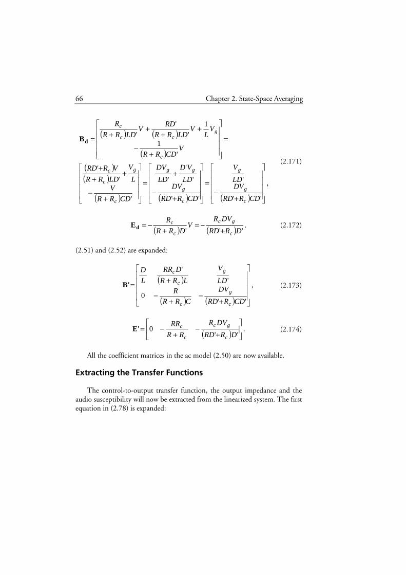
66 Chapter 2. State-Space Averaging
( ) ( )
( )( )( )
( ) ( ) ( ),
''
'
''
'
'
'
'
'
'
'
1
1
'
'
'
+−
=
+−
+=
+−
++
+
=
+−
++
++=
CDRRD
DVLD
V
CDRRD
DVLD
VD
LD
DV
CDRR
VL
V
LDRR
VRRD
VCDRR
VL
VLDRR
RDV
LDRR
R
c
g
g
c
g
gg
c
g
c
c
c
gcc
c
dB
(2.171)
( ) ( ) .''' DRRD
DVRV
DRR
R
c
gc
c
c
+−=
+−=dE (2.172)
(2.51) and (2.52) are expanded:
( )
( ) ( )
,
''0
'
'
+−
+−
+=
CDRRD
DV
CRR
RLD
V
LRR
DRR
L
D
c
g
c
g
c
c
B' (2.173)
( ) .''
0
+−
+−=
DRRD
DVR
RR
RR
c
gc
c
cE' (2.174)
All the coefficient matrices in the ac model (2.50) are now available.
Extracting the Transfer Functions
The control-to-output transfer function, the output impedance and the audio susceptibility will now be extracted from the linearized system. The first equation in (2.78) is expanded:
Chapter 2. State-Space Averaging 67
( ) ( )
( ) ( )
( )
( ) ( )
.)(ˆ
''0
'
'
1'
''
)(ˆ
1
s
CDRRD
DV
CRR
R
LD
V
LRR
DRR
L
D
sCRRCRR
RDLRR
RDs
LRR
DRR
s
c
g
c
g
c
c
cc
cc
c
'u
x
+−
+−
+
•
+++
−
++
+=
−
(2.175)
The matrix inversion in (2.175) is calculated:
( ) ( ) ( )
( ) ( )
( ) ( )
( )
( ) ( )
.)(ˆ
''0
'
'
''
'1
'1'
1)(ˆ
2
22
s
CDRRD
DV
CRR
R
LD
V
LRR
DRR
L
D
sLRR
DRR
CRR
RDLRR
RDs
CRR
LCRR
DRs
CRRs
LRR
DRRs
c
g
c
g
c
c
c
c
c
cc
ccc
c
'u
x
+−
+−
+
•
+++
+−+
+
•
++
+
+
+
+
=
(2.176)
(2.176) is modified to:
68 Chapter 2. State-Space Averaging
( ) ( )
( ) ( ) ( ) ( )
( ) ( ) ( ) ( )
( ) ( )( )
( ) ( )( ) ( )
,)(ˆ
''''
'''
'
''
'''
'''
'''
1)(ˆ
2
2
2
22
2
2
2
22
22
s
CDRRD
DVs
LCDRRDRR
VDDRR
LCRR
RVLCDRRDRR
VRDD
LD
Vs
LCDRR
V
CRR
Rs
LCRR
DRR
LCRR
DRR
LCRR
RDD
LCRR
DR
LRR
DRRs
LCRR
DRR
L
Ds
LCRR
D
sLCRR
CDRRLs
LCRR
DRDRRs
c
g
cc
gc
c
g
cc
gg
c
g
cc
c
c
c
c
cc
c
c
c
c
c
c
c
c
'u
x
+−
++−
+
++++
+
+−
+−
++
++
++
++
+
×+
++
++
+=
(2.177)
( ) ( ) ( ) ( )( )( ) ( )
( )
( )( )
( ) ( ).)(ˆ
'''
'
'1
'
''
1'1
'''
1)(ˆ
2
2
2
s
sLDRDRRDD
RRV
CRRsRRD
RDD
D
V
sRLRR
DDRRRDD
CsRRDCRRsD
LCRRsCDRRLsRRRRDRDs
c
cg
cc
g
c
c
cc
cccc
'u
x
−+
+
++
++
−+
−
+++
•++++++
=
(2.178)
Six transfer functions are now derived from (2.178):
( )
( ) ( ) ( ) ( ),
'''
'
'1
'
)(ˆ)(ˆ
2 LCRRsCDRRLsRRRRDRD
CRRsRRD
RDD
D
V
sd
si
cccc
cc
g
L
++++++
++
++
=
(2.179)
Chapter 2. State-Space Averaging 69
( )( ) ( )
( ) ( ) ( ) ( ),
'''
'''
)(ˆ)(ˆ
2
2
LCRRsCDRRLsRRRRDRD
sLDRDRRDD
RRV
sd
sv
cccc
c
cg
++++++
−+
+
=
(2.180)
( )( ) ( ) ( ) ( )
,'''
1'
)(ˆ)(ˆ
2 LCRRsCDRRLsRRRRDRD
CsRRD
si
si
cccc
c
inj
L
+++++++
=
(2.181)
( )( ) ( ) ( ) ( )
,'''
'
)(ˆ)(ˆ
2
2
LCRRsCDRRLsRRRRDRD
sRLRR
DDRR
si
sv
cccc
c
c
inj
++++++
−+
−
=
(2.182)
( )( )( ) ( ) ( ) ( )
,'''
1
)(ˆ
)(ˆ
2 LCRRsCDRRLsRRRRDRD
CRRsD
sv
si
cccc
c
g
L
++++++++
= (2.183)
( ) ( ) ( ) ( ).
'''
'
)(ˆ)(ˆ
2 LCRRsCDRRLsRRRRDRD
RDD
sv
sv
cccc
g
++++++
=
(2.184)
The second equation in (2.78) is expanded:
70 Chapter 2. State-Space Averaging
( ) .)(ˆ''
0
)(ˆ')(ˆ
sDRRD
DVR
RR
RR
sRR
RD
RR
RRs
c
gc
c
c
cc
c
'u
xy
+−
+−
+
++
=
(2.185)
The control-to-output transfer function is obtained by combining (2.185), (2.179), and (2.180):
( )( )
( ) ( )( )
( ) ( ) ( ) ( ).
'''
1'''
'')(ˆ)(ˆ
)(ˆ)(ˆ'
)(ˆ)(ˆ
2
2
LCRRsCDRRLsRRRRDRD
CsRsLDRDDRRD
RRV
DRRD
DVR
sd
sv
RR
R
sd
si
RR
DRR
sd
sv
cccc
cc
cg
c
gc
c
L
c
co
++++++
+−+
+
==+
−+
++
= K
(2.186)
The output impedance is derived by combining (2.185), (2.181), and (2.182):
( ) ( )
( ) ( ) ( ) ( ).
'''
1'
)(ˆ)(ˆ
)(ˆ)(ˆ'
)(ˆ)(ˆ
)(
2
2
LCRRsCDRRLsRRRRDRD
CsRsRLRR
DDRR
RR
RR
si
sv
RR
R
si
si
RR
DRR
si
svsZ
cccc
cc
c
c
c
injcinj
L
c
c
inj
oout
++++++
+
+
+
==+
++
−+
−
=−=
K(2.187)
The audio susceptibility is calculated by combining (2.185), (2.183), and (2.184):

Chapter 2. State-Space Averaging 71
( )( )( )( ) ( ) ( ) ( )
( ) ( )( )
( ) ( ) ( ) ( )( )
( ) ( ) ( ) ( ).
'''
1'
'''
''1
'''
'1'1
)(ˆ)(ˆ
)(ˆ
)(ˆ'
)(ˆ
)(ˆ
2
2
2
2
LCRRsCDRRLsRRRRDRD
CsRRDD
LCRRsCDRRLsRRRRDRD
CRRDDsRRRRRDDRR
LCRRsCDRRLsRRRRDRD
DDRCRRsDDRRRR
sv
sv
RR
R
sv
si
RR
DRR
sv
sv
cccc
c
cccc
cccc
cccc
ccc
gcg
L
c
c
g
o
+++++++
=++++++
++++
=++++++
++++
=+
++
=
(2.188)
The zero ( )CsRc+1 is added to the transfer function in the case where )(ˆ svo is the output compared to the case where )(ˆ sv is the output. This is
apparent by comparison of (2.188), (2.184), (2.187), (2.182), (2.186), and (2.180). The buck and boost converters exhibit the same property, see Section 2.3 and 2.6. Note that the control-to-output transfer function, (2.186), has a right half plane zero and is not a minimum phase system. This is also the case for the boost converter but not for the buck converter.
2.10 Simulation of a Buck-Boost Converter
In this section, a simulation model for a buck-boost converter is presented. The frequency functions predicted by the transfer functions derived in Section 2.9 are compared with simulation results.
To simulate a buck-boost converter the simulation model shown in Figure 2.5 is used, except the buck converter subsystem is replaced with the buck-boost converter subsystem shown in Figure 2.20.
The parameter values shown in Table 2.6 are used in all the simulations except for )(tvg and )(td . They are of course not constant in the simulations. The values in the table are instead their dc values.
Figure 2.21 shows the Bode plot for the control-to-output transfer function (2.186). The frequency function obtained in the case where the magnitude of the signal dhat is non-zero in the simulations is also shown in the figure. The figure shows that the control-to-output transfer function derived in Section 2.9 agrees closely with the simulation results.

72 Chapter 2. State-Space Averaging
Figure 2.20: The buck-boost converter subsystem.
Figure 2.21: The control-to-output transfer function of a buck-boost converter. Solid line: the analytic model. X: the simulation results.
3 iL
2 iload
1 vo
signal
-1 + -
v 1 g
2 m
Transistor
Rdummy Rc
R
NOT
L
signal +
-
+ i -
+ i - 1
g 2 m
Diode emulator
C
3 delta
2 iinj
1 vg
101
102
103
104
-10
0
10
20
30
40
101
102
103
104
-250
-200
-150
-100
-50
0
Frequency (Hz)
Pha
se (
deg)
; M
agni
tude
(dB
)
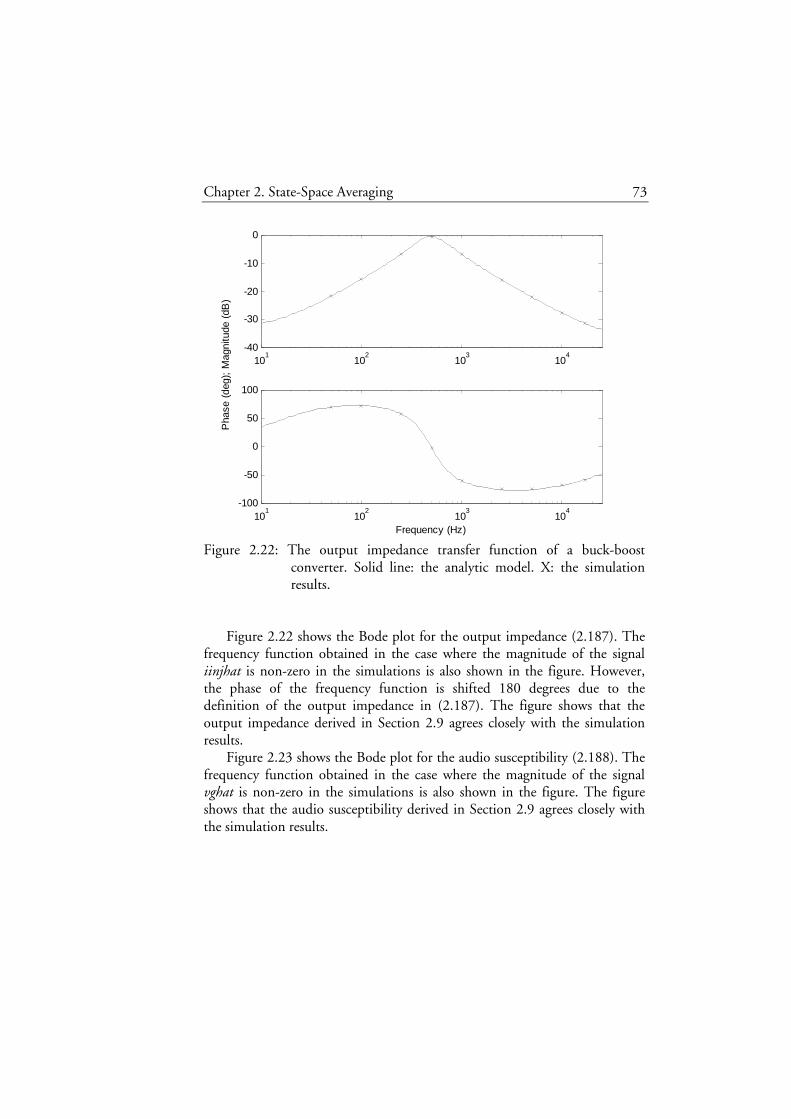
Chapter 2. State-Space Averaging 73
Figure 2.22: The output impedance transfer function of a buck-boost converter. Solid line: the analytic model. X: the simulation results.
Figure 2.22 shows the Bode plot for the output impedance (2.187). The
frequency function obtained in the case where the magnitude of the signal iinjhat is non-zero in the simulations is also shown in the figure. However, the phase of the frequency function is shifted 180 degrees due to the definition of the output impedance in (2.187). The figure shows that the output impedance derived in Section 2.9 agrees closely with the simulation results.
Figure 2.23 shows the Bode plot for the audio susceptibility (2.188). The frequency function obtained in the case where the magnitude of the signal vghat is non-zero in the simulations is also shown in the figure. The figure shows that the audio susceptibility derived in Section 2.9 agrees closely with the simulation results.
101
102
103
104
-40
-30
-20
-10
0
101
102
103
104
-100
-50
0
50
100
Frequency (Hz)
Pha
se (
deg)
; M
agni
tude
(dB
)
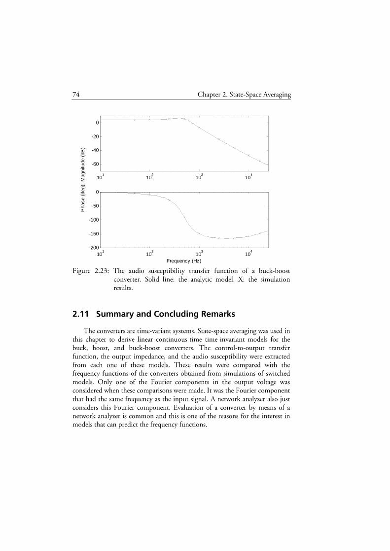
74 Chapter 2. State-Space Averaging
Figure 2.23: The audio susceptibility transfer function of a buck-boost converter. Solid line: the analytic model. X: the simulation results.
2.11 Summary and Concluding Remarks
The converters are time-variant systems. State-space averaging was used in this chapter to derive linear continuous-time time-invariant models for the buck, boost, and buck-boost converters. The control-to-output transfer function, the output impedance, and the audio susceptibility were extracted from each one of these models. These results were compared with the frequency functions of the converters obtained from simulations of switched models. Only one of the Fourier components in the output voltage was considered when these comparisons were made. It was the Fourier component that had the same frequency as the input signal. A network analyzer also just considers this Fourier component. Evaluation of a converter by means of a network analyzer is common and this is one of the reasons for the interest in models that can predict the frequency functions.
101
102
103
104
-60
-40
-20
0
101
102
103
104
-200
-150
-100
-50
0
Frequency (Hz)
Pha
se (
deg)
; M
agni
tude
(dB
)

Chapter 2. State-Space Averaging 75
The conclusion of the comparison is that the models derived by using state-space averaging agree closely with the simulation results at the tested frequencies ( 3,,500,1000 sss fff K ). However, it should be noted that the linearized models are valid only for small signals.


77
Chapter 3 Current-Mode Control
In this chapter we consider models for converters with current-mode control. Various transfer functions are derived and subsequently compared with simulation results. Switched (large-signal) simulation models are utilized. In Chapter 6, some of the derived transfer functions will be approximated and then, in Chapter 7, used to analyze some properties that can be obtained when load current measurements are utilized for control.
3.1 Introduction
In current-mode control, the inductor current is feed back in an inner control loop and the output voltage is feed back in an outer control loop. Current-mode control is also called current programmed control and current-injected control. Descriptions of current-mode control can be found in e.g. Kislovski, Redl and Sokal (1991, Chapter 5), Erickson and Maksimovic (2000, Chapter 12), and Mitchell (1988, Chapter 6).
A large number of continuous-time models for current-mode control have been presented during the years. Some of these models are intended to be accurate also at high frequencies. The models presented by Ridley (1991), Tan and Middlebrook (1995), and Tymerski and Li (1993) are designed to be accurate from dc to half the switching frequency. The main difference between the Ridley and Tan models is the modeling of the current loop gain. Tymerski and Li (1993) presents a state-space model while the Ridley and Tan models uses the PWM switch model (Vorperian, 1990).
In Tymerski (1994), time-varying system theory is used to derive models for the frequency function and they are claimed to be exact for all frequencies. Only the control-to-output frequency function is derived (so far) in the case where current-mode control is utilized. The model is more complicated than
78 Chapter 3. Current-Mode Control
the previously mentioned models. When the control-to-output frequency function of a converter is used to design a controller, the frequency interval dc to half the switching frequency is the most interesting. The previously mentioned models may therefore be good enough when designing a controller.
When an accurate model of current-mode control has been needed, the one presented by Ridley (1991) often has been chosen. An example of this is Lo and King (1999), where the choice was between the Ridley and Tan models. In Lo and King (1999), the Tan model is considered suspect and some other authors have also expressed this opinion.
The operation of current-mode control is explained in Section 3.2. An accurate control-to-current transfer function is reviewed in Section 3.3. In Section 3.4, the Ridley and Tan models are reviewed and compared. These two models utilizes the accurate control-to-current transfer function reviewed in Section 3.3. The Ridley and Tan models are used to obtain the control-to-output transfer function, the output impedance, and the audio susceptibility of the buck converter with current-mode control and these derivations are also presented in Section 3.4. These transfer functions are compared with results from simulations of a buck converter in Section 3.5. The results of the comparison are also explained in this section. In Section 3.6, the Ridley model is used to obtain the transfer functions for the boost converter with current-mode control. These transfer function are also compared with results from simulations of a boost converter in Section 3.6. The corresponding work is made for the buck-boost converter in Section 3.7. A summary and concluding remarks are presented in Section 3.8.
3.2 Operation of Current-Mode Control
The operation and implementation of current-mode control are discussed in this section.
In current-mode control, two control loops are used (Redl and Sokal, 1986). See Figure 3.1. The inner loop is fast and controls the inductor current, )(tiL . The outer loop is slower and controls the output voltage,
)(tvo . The inductor current is fed back via the current controller in the inner loop while the output voltage is fed back via the voltage controller in the outer loop. The voltage controller has the reference signal )(tvref . The voltage controller tries to get )(tvo equal to )(tvref by changing its control
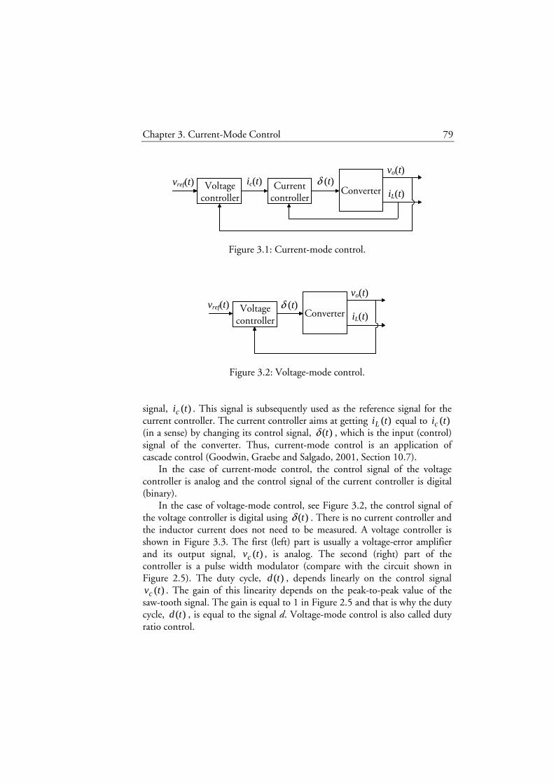
Chapter 3. Current-Mode Control 79
Figure 3.1: Current-mode control.
Figure 3.2: Voltage-mode control.
signal, )(tic . This signal is subsequently used as the reference signal for the current controller. The current controller aims at getting )(tiL equal to )(tic (in a sense) by changing its control signal, )(tδ , which is the input (control) signal of the converter. Thus, current-mode control is an application of cascade control (Goodwin, Graebe and Salgado, 2001, Section 10.7).
In the case of current-mode control, the control signal of the voltage controller is analog and the control signal of the current controller is digital (binary).
In the case of voltage-mode control, see Figure 3.2, the control signal of the voltage controller is digital using )(tδ . There is no current controller and the inductor current does not need to be measured. A voltage controller is shown in Figure 3.3. The first (left) part is usually a voltage-error amplifier and its output signal, )(tvc , is analog. The second (right) part of the controller is a pulse width modulator (compare with the circuit shown in Figure 2.5). The duty cycle, )(td , depends linearly on the control signal
)(tvc . The gain of this linearity depends on the peak-to-peak value of the saw-tooth signal. The gain is equal to 1 in Figure 2.5 and that is why the duty cycle, )(td , is equal to the signal d. Voltage-mode control is also called duty ratio control.
vref(t) Voltage controller
Currentcontroller
vo(t) ic(t) δ (t)
iL(t) Converter
vref(t) Voltagecontroller
vo(t) δ (t)
iL(t) Converter

80 Chapter 3. Current-Mode Control
Figure 3.3: A voltage controller in voltage-mode control.
Figure 3.4: A current controller in current-mode control. A typical current controller in current-mode control is implemented as
shown in Figure 3.4. The peak inductor current is controlled and the control method is therefore called peak current-mode control. This is the most common type of current-mode control and the word “peak” is often left out. If Figure 3.4 and Figure 3.3 are compared, the current controller seems to consist only of a modulator. Kislovski, Redl and Sokal (1991, Chapter 5) use the name current modulator instead of current controller. Average current-mode control is another type of current-mode control (Kislovski, Redl and
vo(t)
vref(t) vc(t)
δ (t) Q S
R
Sawtooth andpulse generator
iL(t)
ic(t)
δ (t) Q S
R
Sawtooth andpulse generator
ie(t)

Chapter 3. Current-Mode Control 81
Figure 3.5: The waveforms of the signals in a current controller in (peak)
current-mode control.
Sokal, 1991, Chapter 5). The first part of the current controller in average current-mode control is a current-error amplifier. It may in this case not be suitable to call the current controller a current modulator since one may consider it consist of more than a modulator (compare with the voltage controller in voltage-mode control). The name current controller may therefore be seen as more general and it is used in this thesis. The modulator is seen as a (large or small) part of the current controller.
The operation of the current controller in (peak) current-mode control shown in Figure 3.4 will now be explained. For a moment assume that the saw-tooth signal, )(tie , is not present. The period of the signal from the pulse generator is equal to sT and the signal sets the SR-latch. Each time this occurs, the transistor is turned on and the inductor current, )(tiL , starts to increase as shown in Figure 3.5. When )(tiL becomes greater than the signal
)(tic , the SR-latch is reset and )(tiL then decreases until a new set pulse is generated. This is the same function as the pulse width modulator in Figure 2.5 and Figure 3.3 except the inductor current, )(tiL , replaces the saw-tooth signal. Compare the waveforms shown in Figure 3.5 and Figure 2.7. The signal )(tic is the reference signal of the current controller. The current controller tries to get )(tiL equal to )(tic in the sense that it is the peak value of )(tiL that is of interest. In average current-mode control, it is the average value of )(tiL that is of interest. The current controller in (peak) current-mode control is fast since it manages to get the peak value of )(tiL equal to
t 0 Tsd(t) Ts
iL(t)+ie(t), ic(t)
t
δ (t)
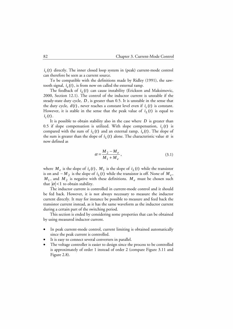
82 Chapter 3. Current-Mode Control
)(tic directly. The inner closed loop system in (peak) current-mode control can therefore be seen as a current source.
To be compatible with the definitions made by Ridley (1991), the saw-tooth signal, )(tie , is from now on called the external ramp.
The feedback of )(tiL can cause instability (Erickson and Maksimovic, 2000, Section 12.1). The control of the inductor current is unstable if the steady-state duty cycle, D , is greater than 0.5. It is unstable in the sense that the duty cycle, )(td , never reaches a constant level even if )(tic is constant. However, it is stable in the sense that the peak value of )(tiL is equal to
)(tic . It is possible to obtain stability also in the case where D is greater than
0.5 if slope compensation is utilized. With slope compensation, )(tic is compared with the sum of )(tiL and an external ramp, )(tie . The slope of the sum is greater than the slope of )(tiL alone. The characteristic value α is now defined as
,1
2
e
e
MM
MM
+−
=α (3.1)
where eM is the slope of )(tie , 1M is the slope of )(tiL while the transistor is on and 2M− is the slope of )(tiL while the transistor is off. None of eM ,
1M , and 2M is negative with these definitions. eM must be chosen such that 1<α to obtain stability.
The inductor current is controlled in current-mode control and it should be fed back. However, it is not always necessary to measure the inductor current directly. It may for instance be possible to measure and feed back the transistor current instead, as it has the same waveform as the inductor current during a certain part of the switching period.
This section is ended by considering some properties that can be obtained by using measured inductor current.
• In peak current-mode control, current limiting is obtained automatically
since the peak current is controlled. • It is easy to connect several converters in parallel. • The voltage controller is easier to design since the process to be controlled
is approximately of order 1 instead of order 2 (compare Figure 3.11 and Figure 2.8).

Chapter 3. Current-Mode Control 83
• The audio susceptibility can become low for a buck converter by choosing proper slope compensation (compare Figure 4.14 and Figure 2.10).
• A disadvantage is that the output impedance is high (compare Figure 3.12 and Figure 2.9).
3.3 An Accurate Control-to-Current Transfer Function
The high-frequency extensions in the Ridley and Tan models are based on the accurate control-to-current transfer function that is reviewed in this section.
In Figure 3.5, )(tie is added to )(tiL but the same function is obtained if )(tie is subtracted from )(tic and this is used in Figure 3.6(a). Figure 3.6(a) shows the waveforms of the signals )(tic , )()( titi ec − , and two different versions of the inductor current. The first version (solid line) shows the inductor current waveform in steady state, i.e. in the case where there are no perturbations of )(tic . The second version (dashed line) shows the inductor current waveform in the case where there is a step perturbation in
)(tic as shown in Figure 3.6(a). The transistor is assumed to turn on at the points snTt = , where n is an integer. The transistor will then turn off at the points ( ) sTDnt += in steady state. It is assumed that the changes in the input voltage and the output voltage are negligible so that the slopes of the inductor current can be considered constant.
In Figure 3.6(a), )(tic was perturbed, and this perturbation, )(ˆ tic , is shown in Figure 3.6(b). This perturbation results in a perturbation in the inductor current that is equal to the difference between the two versions of the inductor current in Figure 3.6(a). The perturbation in the inductor current, )(ˆ tiL , is shown in Figure 3.6(c).
An approximation of )(ˆ tiL is shown in Figure 3.6(d). This approximation causes an error but the integral of this error is small compared to the integral of )(ˆ tiL if the amplitude of )(ˆ tiL is small. The reason for this is that the time needed to change from one level to the next is short compared to sT in this case. If we search for a linearized model, the use of the waveform in Figure 3.6(d) instead of the waveform in Figure 3.6(c) does not cause an approximation since:

84 Chapter 3. Current-Mode Control
Figure 3.6: Different versions of the currents in a current controller.
Ts(k+1+D) t
Ts(k+1) Ts(k-1+D)
iL(t)
ic(t)
ic(t)-ie(t)
(a)
Ts(k+1+D) t
Ts(k+D) Ts(k-1+D) (b)
ic(t)
Ts(k+1+D) t
Ts(k+D) Ts(k-1+D) (c)
iL(t)
k+1 n
k k-1 (f)
iL(n)
Ts(k+1+D) t
Ts(k+D) Ts(k-1+D)
iL(t) (app.)
(d)
k+1 n
k k-1 (e)
ic(n)
^
^
^
^
^
Chapter 3. Current-Mode Control 85
Figure 3.7: An enlargement of a part of Figure 3.6(a).
( ) 0)(ˆ
)(lim
0)(ˆmax=
∫∫
→ dtti
dtterror
LtiL
. (3.2)
The signal )(tic affects the waveform of the inductor current. If the
changes in )(tic are small, the value of )(tic is important only in a small surrounding of the points ( ) sTDnt += If the changes of )(tic in these surroundings are slow, only a sampled version of )(tic (or )(ˆ tic ) is needed to obtain an accurate model. A sampled version of )(ˆ tic is shown in Figure 3.6(e) and it is denoted )(ˆ nic . To be spared from introducing new variable names, the sampled (discrete-time) version of a continuous-time signal is denoted by the same name as the continuous-time signal, which is not a formally correct notation.
A sampled version of the approximate )(ˆ tiL is shown in Figure 3.6(f) and it is denoted )(ˆ niL . An expression for )(ˆ niL will now be derived. A small part of Figure 3.6(a) is enlarged and it is shown in Figure 3.7. The following two equations are obtained from Figure 3.7:
,)1(ˆ)(ˆ
1 tMtMkiki ecL ∆+∆=+− (3.3)
.)1(ˆ)(ˆ21 tMtMkiki LL ∆+∆=+− (3.4)
t
iL(k+1)
Ts(k+1+D)
iL(k)
ic(k+1)
M1
-M2
-M2
M1
-Me
∆t
^
^
^
86 Chapter 3. Current-Mode Control
We first solve from (3.3):
( ) ,)1(ˆ)(ˆ1
1
tkikiMM
t cLe
+−+
=∆ (3.5)
and insert the result into (3.4):
( ) ( )
( ) .)1(ˆ1)(ˆ)1(ˆ1
)(ˆ
)1(ˆ)(ˆ1)(ˆ)1(ˆ
1
21
1
1
1
21
1
1
121
+++−=+
++
+++
−
+
++
−++
=+−+
+−=+
kikikiMM
MM
MM
MM
kiMM
MM
MM
MM
kikiMM
MMkiki
cLcee
e
Lee
e
cLe
LL
αα
(3.6)
The variable k is substituted by n in (3.6):
( ) .)1(ˆ1)(ˆ)1(ˆ +++−=+ ninini cLL αα (3.7)
where α is defined in (3.1). The difference equation (3.7) is stable if 1<α , which is in agreement with the condition presented in Section 3.2. Remember that (3.7) is valid only for small )(ˆ tic and )(ˆ niL , so (3.7) can not be used to claim that )(ˆ niL approaches infinity if 1>α . The dc gain of (3.7) is equal to 1, which is evident by setting )1(ˆ +niL equal to )(ˆ niL . This result should be used with some care. The reason is that a constant 0)(ˆ ≠tic may affect the output voltage such that its change is not negligible, which is an assumption in the derivation of (3.7).
The following discrete-time transfer function is obtained from the Z-transform of (3.7):
( )
αα
++
==z
z
zi
zizH
c
L 1
)(ˆ)(ˆ
)( (3.8)
)(ˆ ziL and )(ˆ zic denote the Z-transform of )(ˆ niL and )(ˆ nic . To be
spared from introducing new variable names, the Z-transform of a signal is denoted by the same name as the signal, e.g. )()( ziniZ = .

Chapter 3. Current-Mode Control 87
The approximate perturbed inductor current shown in Figure 3.6(d) is reconstructed from )(ˆ niL by using a zero-order-hold circuit. The continuous-time control-to-current transfer function is therefore (Åström and Wittenmark, 1997, Section 7.7):
( ) ( )
s
e
e
e
Tsi
sisF
s
s
s sT
sT
sT
sc
Lh
−−+
+==
111
)(ˆ)(ˆ
)(α
α (3.9)
The first fraction in (3.9) represents the sampling of )(ˆ tic . The second
fraction is )(zH transformed into continuous-time domain by substituting z with ssTe . The third fraction is the transfer function of a zero-order-hold circuit. Note that there are other frequency components in )(ˆ tiL than (3.9) predicts (Perreault and Verghese, 1997). If )(ˆ tic is a sinusoidal, the model only predicts the Fourier component that is of the same frequency as )(ˆ tic . The same conclusion was made about the models derived in Chapter 2 (see Section 2.4).
Once again, note that the derivation of (3.9) is made with the assumption that the changes in the input and output voltage are negligible. The high-frequency extensions in the Ridley and Tan models are based on the accurate control-to-current transfer function (3.9).
3.4 The Ridley and Tan Models Applied to the Buck Converter
In this section, the Ridley and Tan models are reviewed and compared. One block diagram is here used for both of these models. However, the contents in the blocks are (of course) not the same for the two models. General expressions for the control-to-output transfer function, the output impedance, and the audio susceptibility are derived from the block diagram. These general expressions are then applied to the buck converter. The obtained expressions are finally used to derive expressions according to the Ridley and Tan models.
A Brief Review
Both the Ridley and Tan models are unified models, i.e. they can be applied to different types of converter topologies. The block diagram in

88 Chapter 3. Current-Mode Control
Figure 3.8: A small-signal model of the current controller and the converter.
Figure 3.8 is used to compare the Ridley and Tan models. Both are small-signal models and, therefore, the linearized model of the converter is included in Figure 3.8.
The model of the current controller consists of six blocks. The iR blocks will be explained later in this subsection. )(sFm is the transfer function of the modulator. Changes in the input and output voltages affect the control and this effect are modeled with the feedforward gains fk and rk . Note that the input and output voltages are not fed forward in Figure 3.1. The reason why they are needed in Figure 3.8 is that there are Fourier components missing in the signal )(ˆ1 siL L
− compared the signal )(tiL in Figure 3.1 (see Section 2.4). It is not just the dc component that is missing. The input and output voltages affect the slopes of the inductor current in each switching period, which is an important factor in the current controller. The use of )(ˆ svg and
)(ˆ svo in the small-signal model of the current controller therefore complements )(ˆ siL so that the waveform of )(tiL is better known. The feedforward gains are in the Ridley and Tan models calculated in a way that makes the amplification of the closed loop system correct at dc. In Section 3.5, it will be shown that this way introduces a modeling error at high frequencies.
Converter iL(s) ^
vo(s) ^ vg(s) ^
Fm(s) kr kf
vc(s) ^
He(s)
d(s) ^
Ri
Ri
ic(s) ^

Chapter 3. Current-Mode Control 89
The high-frequency extensions in the Ridley and Tan models are based on the accurate control-to-current transfer function (3.9). )(sHe is used to include the high-frequency extension in the Ridley model and it is calculated to be:
.1
)(−
=ssT
se
e
sTsH (3.10)
The Ridley model utilizes an approximation of (3.10). The approximation:
,
1
1
2
2
2
2
nzn
nznsT
s
Q
s
s
Q
s
e s
ωω
ωω
+−
++≈− (3.11)
where
,2
π−=zQ (3.12)
.s
n T
πω = (3.13)
is used both by Ridley and Tan to replace the exponential functions. The approximation error of (3.11) is zero at dc and half the switching frequency,
nω :
,
01
0
1
1
2
2
2
2
jse
js
s
Q
s
s
Q
s
ssT
nzn
nzn
===
=
+−
++−
ωω
ωω
90 Chapter 3. Current-Mode Control
.1
11
11
1
1
2
2
2
2
n
sT
z
z
n
nzn
nzn
jse
Q
jQ
j
js
s
Q
s
s
Q
s
s
ω
ωωω
ωω
==−=
−−
−+=
=
+−
++−
By combining (3.10) and (3.11), the approximate )(sHe is:
,12
1
1
1
1
1
)(
2
22
2
2
2
2
2
2
2
2
2
nzn
zn
nzns
nzn
nzn
nzn
nzn
se
s
Q
s
Q
s
s
Q
ssT
s
Q
s
s
Q
s
s
Q
s
s
Q
s
sTsH
ωωω
ωω
ωω
ωω
ωω
ωω
++=−
++
=
++
++−
++
+−=
(3.14)
By combining (3.9) and (3.11), an approximate expression for )(sFh is
obtained:
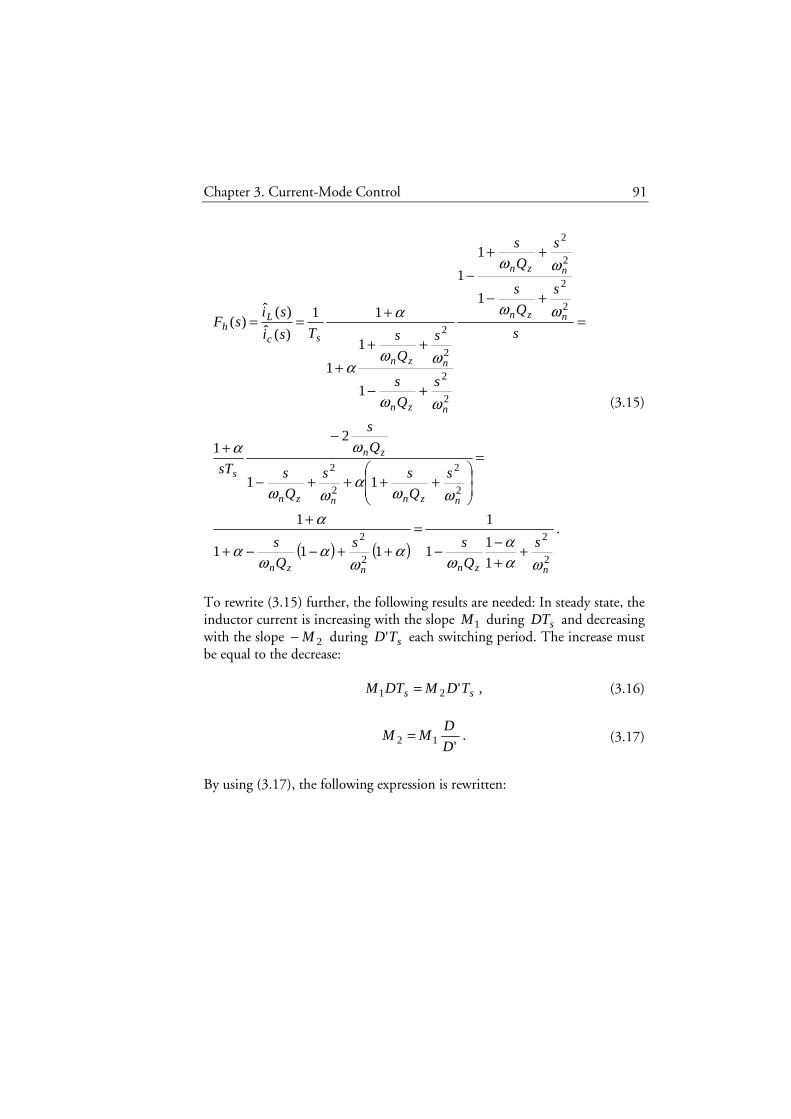
Chapter 3. Current-Mode Control 91
( ) ( ).
1
11
1
111
1
11
21
1
1
1
1
1
1
11
)(ˆ)(ˆ
)(
2
2
2
2
2
2
2
2
2
2
2
2
2
2
2
2
nznnzn
nznnzn
zn
s
nzn
nzn
nzn
nzn
sc
Lh
s
Q
ss
Q
s
s
Q
ss
Q
s
Q
s
sT
s
s
Q
s
s
Q
s
s
Q
s
s
Q
sTsi
sisF
ωαα
ωα
ωα
ωα
αωω
αωω
ωα
ωω
ωω
ωω
ωωα
α
++−−
=++−−+
+
=
++++−
−+
=+−
++−
+−
+++
+==
(3.15)
To rewrite (3.15) further, the following results are needed: In steady state, the inductor current is increasing with the slope 1M during sDT and decreasing with the slope 2M− during sTD' each switching period. The increase must be equal to the decrease:
,'21 ss TDMDTM = (3.16)
.'12 D
DMM = (3.17)
By using (3.17), the following expression is rewritten:

92 Chapter 3. Current-Mode Control
( )
( ) ,1'21'2'1''2'
'
'2'
'
2'
2
1
1
111
1
11
11
11
21
21
1
2
1
1
1
2
1
1
−
+=+−−=+−
=++−
=+
+−
=+
+−=
+−
+++
+−
−++
=+−
DM
MD
M
MDDD
M
MDD
DDM
DMDMDM
D
DMM
MD
DMM
MM
MMM
MM
MM
MM
MM
MM
MM
MM
MM
eee
ee
e
e
e
e
e
e
e
e
e
αα
(3.18)
(3.15) is now rewritten by using (3.18):
,
1
1
1'212
1
1
)(ˆ)(ˆ
)(
2
2
2
2
1
nn
n
e
n
c
Lh
s
Q
s
sD
M
Mssi
sisF
ωω
ωωπ
++
=
+
−
++
==
(3.19)
where
( ) ,5.0'
1−
=Dm
Qcπ
(3.20)
.11M
Mm e
c += (3.21)
The high-frequency extension in the Tan model is obtained by including
a pole in )(sFm . Tan and Middlebrook (1995) present the following model for the buck converter:

Chapter 3. Current-Mode Control 93
( ),
12
'
1)(
+
−+
=
ps
ge
ms
TL
VDDM
sF
ω
(3.22)
,2
'
L
TDDk s
f −= (3.23)
,0=rk (3.24)
,1)( =sHe (3.25)
,1Ω=iR (3.26)
.Q
np
ωω = (3.27)
In a practical current-mode controller, the inductor current is measured
and transformed to a voltage signal. Voltage signals also represent the control signal and the external ramp signal. Ridley models this by including a gain,
iR , in the inductor current feedback loop. Tan does not model this and iR is therefore set to 1 in (3.26). The following variables are used in the Ridley model:
,)(ˆ)(ˆ siRsv cic = (3.28)
,1MRS in = (3.29)
,2MRS if = (3.30)
.eie MRS = (3.31)
Ridley (1990a) presents the following model for the buck converter:
( ) ,11
)(sncsen
mm TSmTSSFsF =
+== (3.32)
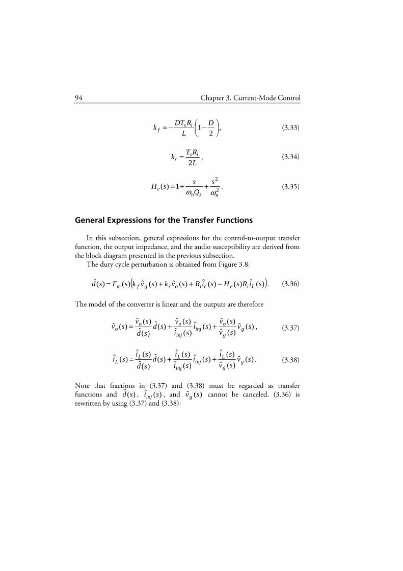
94 Chapter 3. Current-Mode Control
,2
1
−−= D
L
RDTk is
f (3.33)
,2L
RTk is
r = (3.34)
.1)(2
2
nzne
s
Q
ssH
ωω++= (3.35)
General Expressions for the Transfer Functions
In this subsection, general expressions for the control-to-output transfer function, the output impedance, and the audio susceptibility are derived from the block diagram presented in the previous subsection.
The duty cycle perturbation is obtained from Figure 3.8:
( ).)(ˆ)()(ˆ)(ˆ)(ˆ)()(ˆ siRsHsiRsvksvksFsd Lieciorgfm −++= (3.36)
The model of the converter is linear and the outputs are therefore
,)(ˆ)(ˆ
)(ˆ)(ˆ
)(ˆ)(ˆ
)(ˆ)(ˆ)(ˆ
)(ˆ svsv
svsi
si
svsd
sd
svsv g
g
oinj
inj
ooo ++= (3.37)
.)(ˆ)(ˆ
)(ˆ)(ˆ
)(ˆ)(ˆ
)(ˆ)(ˆ)(ˆ
)(ˆ svsv
sisi
si
sisd
sd
sisi g
g
Linj
inj
LLL ++= (3.38)
Note that fractions in (3.37) and (3.38) must be regarded as transfer functions and )(ˆ sd , )(ˆ siinj , and )(ˆ svg cannot be canceled. (3.36) is rewritten by using (3.37) and (3.38):
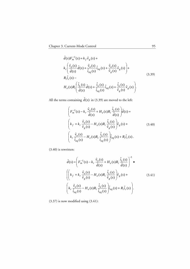
Chapter 3. Current-Mode Control 95
.)(ˆ)(ˆ
)(ˆ)(ˆ
)(ˆ)(ˆ
)(ˆ)(ˆ)(ˆ
)(
)(ˆ
)(ˆ)(ˆ
)(ˆ)(ˆ
)(ˆ)(ˆ
)(ˆ)(ˆ)(ˆ
)(ˆ)()(ˆ 1
++
−
+
++
+=−
svsv
sisi
si
sisd
sd
siRsH
siR
svsv
svsi
si
svsd
sd
svk
svksFsd
gg
Linj
inj
LLie
ci
gg
oinj
inj
oor
gfm
(3.39)
All the terms containing )(ˆ sd in (3.39) are moved to the left:
.)(ˆ)(ˆ)(ˆ)(ˆ
)()(ˆ)(ˆ
)(ˆ)(ˆ
)(ˆ)(
)(ˆ
)(ˆ
)(ˆ)(ˆ)(ˆ
)()(ˆ)(ˆ
)(1
siRsisi
siRsH
si
svk
svsv
siRsH
sv
svkk
sdsd
siRsH
sd
svksF
ciinjinj
Lie
inj
or
gg
Lie
g
orf
Lie
orm
+
−
+
−+
=
+−−
(3.40)
(3.40) is rewritten:
.)(ˆ)(ˆ)(ˆ)(ˆ
)()(ˆ)(ˆ
)(ˆ)(ˆ
)(ˆ)(
)(ˆ
)(ˆ
)(ˆ)(ˆ
)()(ˆ)(ˆ
)()(ˆ1
1
+
−
+
−+
•
+−=
−−
siRsisi
siRsH
si
svk
svsv
siRsH
sv
svkk
sd
siRsH
sd
svksFsd
ciinjinj
Lie
inj
or
gg
Lie
g
orf
Lie
orm
(3.41)
(3.37) is now modified using (3.41):

96 Chapter 3. Current-Mode Control
.)(ˆ)(ˆ
)(ˆ)(ˆ
)(ˆ)(ˆ
)(ˆ)(ˆ)(ˆ)(ˆ
)()(ˆ)(ˆ
)(ˆ)(ˆ
)(ˆ)(
)(ˆ
)(ˆ
)(ˆ)(ˆ
)()(ˆ)(ˆ
)()(ˆ)(ˆ
)(ˆ
1
1
svsv
svsi
si
sv
siRsisi
siRsH
si
svk
svsv
siRsH
sv
svkk
sd
siRsH
sd
svksF
sd
svsv
gg
oinj
inj
o
ciinjinj
Lie
inj
or
gg
Lie
g
orf
Lie
orm
oo
+
+
+
−
+
−+
•
+−=
−−
(3.42)
The control-to-output transfer function of the closed loop system, which
includes the converter and the current controller, is obtained from (3.42):
.
)(ˆ)(ˆ
)(ˆ)(ˆ
)()(ˆ)(ˆ
)(
)(ˆ)(ˆ
)()(ˆ)(ˆ
)()(ˆ)(ˆ
)(ˆ)(ˆ
111
11
−−−
−−
+−
=
+−=
sd
sv
sd
siRsHk
sd
svsF
R
Rsd
siRsH
sd
svksF
sd
sv
si
sv
oLier
om
i
iL
ieo
rmo
c
o
(3.43)
The subscript ol will be used for the converter transfer functions, i.e. for the open loop system. When otherwise obvious the subscript will be excluded. The output impedance of the closed loop system is obtained from (3.42):
.)(ˆ)(ˆ
)(ˆ)(ˆ
)(ˆ)(ˆ
)()(ˆ)(ˆ
)(
)(ˆ)(ˆ
)()(ˆ)(ˆ
)(ˆ)(ˆ
)(
111 olinj
o
oLier
om
olinj
Lie
olinj
or
inj
oout
si
sv
sd
sv
sd
siRsHk
sd
svsF
si
siRsH
si
svk
si
svsZ
−
+−
−
−
=−=
−−−
(3.44)

Chapter 3. Current-Mode Control 97
The audio susceptibility of the closed loop system can be obtained from (3.42):
.)(ˆ
)(ˆ
)(ˆ)(ˆ
)(ˆ)(ˆ
)()(ˆ)(ˆ
)(
)(ˆ
)(ˆ)(
)(ˆ
)(ˆ
)(ˆ
)(ˆ
111 olg
o
oLier
om
olg
Lie
olg
orf
g
o
sv
sv
sd
sv
sd
siRsHk
sd
svsF
sv
siRsH
sv
svkk
sv
sv
+
+−
−
+
=
−−−
(3.45)
Transfer Functions for the Buck Converter
The general expressions for the control-to-output transfer function, the output impedance, and the audio susceptibility derived in the previous subsection are in this subsection applied to the buck converter.
For the buck converter, (3.43) is rewritten by using (2.83) and (2.90):
( )( )
( )( )
( ) ( )( )
( ),
)(
1
1)(1)()(
1
1
1)(
1
)()(
)(ˆ)(ˆ
1
1
sden
CsRR
CRRssHCsRRR
k
V
sden
R
sF
CsRR
CsRR
CRRsRsHk
CsRRV
sdensF
R
si
sv
c
ceci
r
g
ol
i
m
c
c
cier
cg
olm
i
c
o
+
=++++−
+
=
+++
+−+
=
−
−
(3.46)
where

98 Chapter 3. Current-Mode Control
( ) ( )
( ) ( )( ) ,11
)( 2
CRRssLCsRR
LCRRsCRRLsRsden
cc
ccol
++++=++++=
(3.47)
( ) ( )( ) .1)(1)(
)(1111 CRRssHCsRRkRdenVsFR
sden
cecriolgmi ++++−
=−−−−
(3.48)
)(sdenol is the denominator in the open loop transfer functions and )(sden is the denominator in the closed loop transfer functions. For the buck converter, (3.44) can be rewritten by using (2.83), (2.85) (2.90), and (2.91):
( ) ( ) ( )
( )
( )
( ) ( )( ).)(1)(1
)(
1
)(
1
)(
1
)(
)(
1)(
)(
11
)(ˆ)(ˆ
)(
1
1
ssLdenCsRRsHCsRsRLkR
sdensden
CsRR
sden
CsRsRL
sden
sden
CsRRRsH
sden
CsRsRLkCsRRR
si
svsZ
cecri
ol
c
ol
c
ol
cie
ol
crci
inj
oout
++++
•+
=+
+
++
++
=−=
−
−
(3.49)
For the buck converter, (3.45) is modified by using (2.83), (2.87), (2.90), and (2.92):

Chapter 3. Current-Mode Control 99
( )
( ) ( )( )
( )
( ) (( ) ( )( ) ).)(1)(1
)()(
1
)(
1
)(
1
)(
)(
1)(
)(
1
1)(ˆ
)(ˆ
1
1
1
sDdenCRRsDsHCsRRDkR
sdenkRsdensden
CsRR
sden
CsRRD
sden
sden
CRRsDRsH
sden
CsRRDkk
CsRRRsv
sv
cecri
olfiol
c
ol
c
ol
cie
ol
crf
cig
o
+++−+
++
=+
+
++−
++
•+=
−
−
−
(3.50)
Transfer Functions Obtained by Applying the Ridley Model to the Buck Converter
In this subsection, the transfer functions for the buck converter with current-mode control are derived according to the Ridley model.
For the buck converter, the slope of the inductor current while the transistor is on is
.1 L
VVM
og −= (3.51)
The first term in (3.48) is modified by using (3.32), (3.29), (3.51), (2.66), (2.68), (2.39), and (3.47):
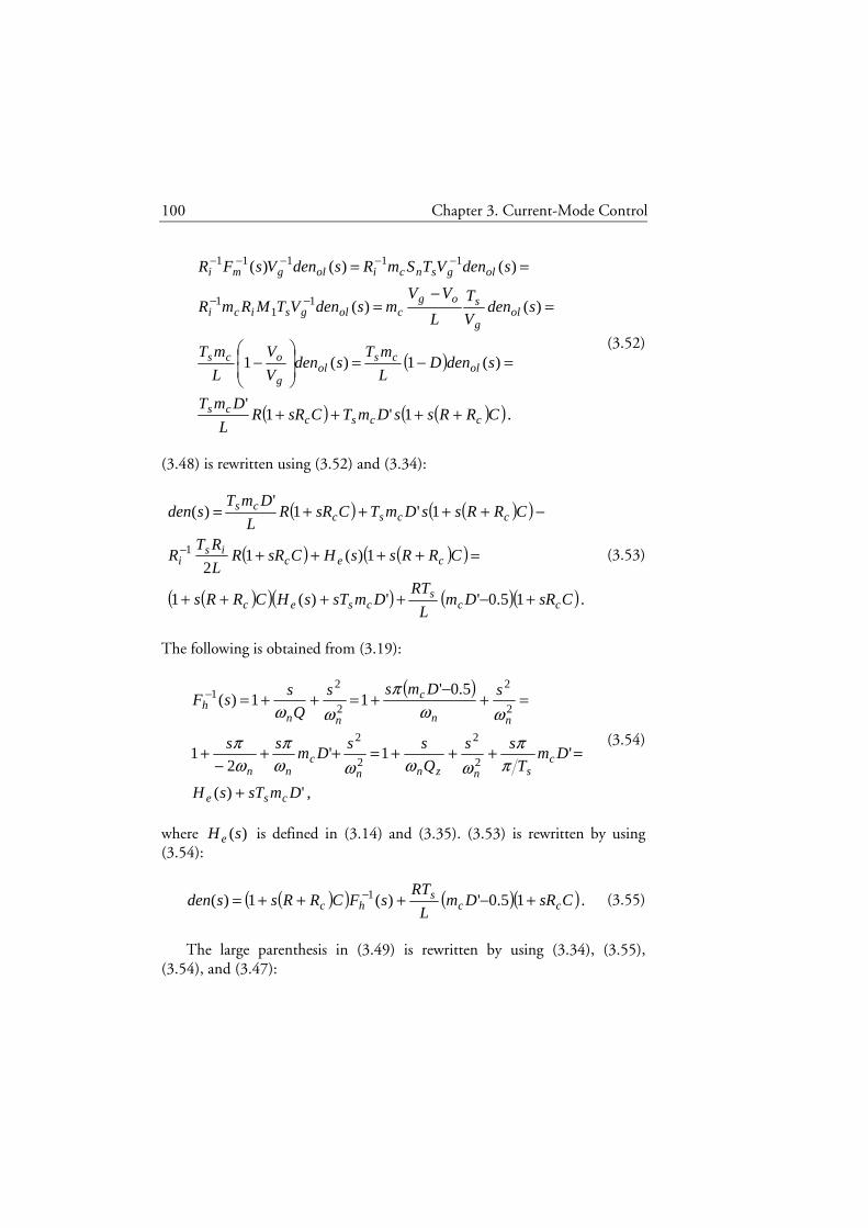
100 Chapter 3. Current-Mode Control
( )
( ) ( )( ) .1'1'
)(1)(1
)()(
)()()(
11
1
11111
CRRssDmTCsRRL
DmT
sdenDL
mTsden
V
V
L
mT
sdenV
T
L
VVmsdenVTMRmR
sdenVTSmRsdenVsFR
ccsccs
olcs
olg
ocs
olg
sogcolgsici
olgsnciolgmi
++++
=−=
−
=−
=
==
−−
−−−−−
(3.52)
(3.48) is rewritten using (3.52) and (3.34):
( ) ( )( )
( ) ( )( )
( )( )( ) ( )( ) .15.0'')(1
1)(12
1'1'
)(
1
CsRDmL
RTDmsTsHCRRs
CRRssHCsRRL
RTR
CRRssDmTCsRRL
DmTsden
ccs
csec
cecis
i
ccsccs
+−++++
=++++
−++++=
− (3.53)
The following is obtained from (3.19):
( )
,')(
'1'2
1
5.0'11)(
2
2
2
2
2
2
2
21
DmsTsH
DmT
ss
Q
ssDm
ss
sDmss
Q
ssF
cse
csnznn
cnn
nn
c
nnh
+
=+++=++−
+
=+−
+=++=−
ππ
ωωωωπ
ωπ
ωωπ
ωω(3.54)
where )(sH e is defined in (3.14) and (3.35). (3.53) is rewritten by using (3.54):
( )( ) ( )( ) .15.0')(1)( 1 CsRDmL
RTsFCRRssden cc
shc +−+++= − (3.55)
The large parenthesis in (3.49) is rewritten by using (3.34), (3.55),
(3.54), and (3.47):
Chapter 3. Current-Mode Control 101
( ) ( )
( )
( )( ) ( )( )
( ) ( )
( )( )( ) ( )( ) .)()()(11)(
)(1
15.0')(2
15.0')(1
1)(2
)(1)(1
111
1
1
1
1
sdensFsFCRRssLCsRRsF
sFCRRssL
CsRRDmsTsHT
s
CsRDmL
RTsFCRRssL
CsRRsHsLL
RTR
ssLdenCsRRsHCsRsRLkR
olhhcch
hc
ccses
ccs
hc
ceis
i
cecri
−−−
−
−
−
−
=++++
=++
++
−++
=
+−+++
++
+
=++++
(3.56)
The large parenthesis in (3.50) is rewritten by using (3.34), (3.55),
(3.54), and (3.47):
102 Chapter 3. Current-Mode Control
( )( )( )
( )( )( )
( )( ) ( )( )
( ) ( )
( ) ( )( )
( )( )( )
( ) ( )( )( )
.)('
)('
11')(
1'
1')(
1)()(
15.0'2
)(
15.0')(1
1)(
12
)(
)(1)(
1)(
1
1
1
1
1
1
11
11
sdenkRDT
LDmD
L
T
sdenDDmL
TkR
CRRssLCsRRDDmL
TsdenkR
CRRsDDmsT
CsRDRDmL
TsdenkR
CRRsDsFsH
CsRDRDmL
T
L
TsdenkR
CsRDmL
RTDsFCRRsD
CRRsDsH
CsRRDL
RTRsdenkR
sDdenCRRsDsH
CsRRDkRsdenkR
olfis
cs
olcs
fi
cccs
olfi
ccs
ccs
olfi
che
ccss
olfi
ccs
hc
ce
cis
iolfi
ce
criolfi
+
=
+
=+++++
=++
+++
=+++−
++
−++
=+−+++
+++
−++
=+++
−++
−
−
−
−
−
−
−−
−−
(3.57)
(3.50) is rewritten by using (3.57):
( )
.)(
1'
)(ˆ
)(ˆ
sden
CsRkRDT
LDmD
L
RT
sv
svcf
isc
s
g
o
+
+
= (3.58)
The transfer functions obtained by applying the Ridley model to the buck
converter are now summarized. The denominators are the same and given by (3.55). The control-to-output transfer function of the closed loop system is given directly by (3.46). The output impedance of the closed loop system is obtained by combining (3.49) and (3.56). The audio susceptibility of the
Chapter 3. Current-Mode Control 103
closed loop system is obtained by combining (3.58) and (3.33). The results are:
( )
,)(
1)(ˆ
)(ˆ
)(ˆ)(ˆ
sden
CsRR
Rsv
sv
si
sv c
ic
o
c
o +== (3.59)
( )
,)(
)(1)(
1
sden
sFCsRRsZ hc
out
−+= (3.60)
( )
,)(
12
1'
)(ˆ
)(ˆ
sden
CsRD
DmDL
RT
sv
svcc
s
g
o
+
−−=
(3.61)
where
( )( ) ( )( ) .15.0')(1)( 1 CsRDmL
RTsFCRRssden cc
shc +−+++= − (3.62)
and )(sFh is defined in (3.19).
Transfer Functions Obtained by Applying the Tan Model to the Buck Converter
In this subsection, the transfer functions for the buck converter with current-mode control are derived according to the Tan model.
(3.48) is rewritten by using (3.22), (3.24)-(3.27), and (3.47):
( )
( ) ( )( )( ) ( )( ) .111
12
')( 1
CRRsCRRssLCsRR
VQ
sT
L
VDDMsden
ccc
gn
sg
e
+++++++
•
+
−+= −
ω (3.63)
One part of (3.63) is first rewritten by using (3.21), (3.51), (2.66), (2.68), and (2.39):

104 Chapter 3. Current-Mode Control
( ) ( ) ( )
( ) ( )
( )
( ) .5.0'2
''
2
'''
2
'11
1
2
'1
2
'1
2
'
1
11
1
−=
+−
=
−+−=
−+−
−
=
−+−
−
=
−+−=
−+
−
−−
DmL
TDDDm
L
T
DDDDm
L
TT
L
DDm
V
V
L
VTL
VDDm
L
VV
VTL
VDDmMVT
L
VDDM
cs
cs
cs
scg
o
gsg
cog
gsg
cgsg
e
(3.64)
(3.63) can now be rewritten by using (3.64), (3.20), (3.13), and (3.19):
Chapter 3. Current-Mode Control 105
( ) ( )( ) ( )( )( ) ( )( )
( )
( ) ( )( )( ) ( )( )
( ) ( ) ( ) ( )( )
( ) ( )( ) ( )( )
( )( ) ( )
( )
( )( )( )
( )
( )( ) ( ) .12
15.0')(1
12
15.0'
5.0'
111
15.0'
5.0'11
111
15.0'15.0'
111
5.0'
111
5.0'15.0')(
1
2
2
2
2
CsRsDmL
RTsFCRRs
CsRsDmL
RT
s
DmT
sCRRs
CsRs
DmL
RT
TssDmTCRRs
CRRsCRRsTs
CsRRL
sT
CRRssDmTCsRRDmL
T
CRRsCRRssLCsRR
L
sTDm
L
T
CRRsCRRssLCsRR
Dm
sDm
L
Tsden
cn
cs
hc
cn
cs
n
cs
c
cn
cs
n
scsc
ccn
sc
n
s
ccsccs
ccc
n
sc
s
ccc
cnc
s
+
−−+++
=+
−−
+
+
−
+++
=+
+−
+
+−+++
=+++++++
+++−++−
=+++++++
•
+−
=+++++++
•
−
+−=
−
πω
πω
ωπ
π
πω
πω
πωπω
πω
πω
(3.65)
The large parenthesis in (3.49) is modified by using (3.24), (3.25), (3.65),
(3.14), (3.54), and (3.47):
106 Chapter 3. Current-Mode Control
( ) ( )( ) ( )( )
( )
( )
( )( )
( )
( )( )( ) ( ) ( )( )
( ) ( )( ) .)()()(11)(
)(11')(
)(1
1'2
1
)(1
12
15.0'1
12
15.0'
)(11
)(1)(1
111
1
1
2
1
1
1
sdensFsFCRRssLCsRRsF
sFCRRssLCsRRDmsTsH
sFCRRssL
CsRRDmsTT
s
T
s
sFCRRssL
CsRRsDmsT
CsRsDmL
RTsL
sFCRRssLCsRR
ssLdenCsRRsHCsRsRLkR
olhhcch
hcccse
hc
ccssns
hc
cn
cs
cn
cs
hcc
cecri
−−−
−
−
−
−
−
=++++
=+++++
=++
++
++
−+
=++
++
−−+
=+
−−
+++++
=++++
πω
πω
πω
(3.66)
The large parenthesis in (3.50) is altered by using (3.24)-(3.26), (3.65),
(3.19), (3.20), (3.13), and (3.47):

Chapter 3. Current-Mode Control 107
( )( )( )
( )( ) ( )( )
( )
( ) ( )( )
( )
( )( )
( )
( ) ( )( )( )
.)(2
12
1'
)(2
15.0'
)(
112
15.0'
)(
12
15.0'
15.0')(
12
15.0'
15.0'11
)(
12
15.0'
)(11)(
)(1)(
1)(
2
2
1
11
sdenskDT
LDmD
L
T
sdensDmDL
T
sdenk
CRRssLCsRRsDmDL
T
sdenk
CsRRsDmDL
T
CRRsDs
DmsTsdenk
CsRRsDmDL
T
CRRsDs
DmT
s
sdenk
CsRsDmL
RTD
sFCRRsDCRRsDsdenk
sDdenCRRsDsH
CsRRDkRsdenkR
oln
fs
cs
oln
cs
olf
ccn
cs
olf
cn
cs
cn
csolf
cn
cs
cn
cs
olf
cn
cs
hccolf
ce
criolfi
−−+
=
−−
+
=++++
−−
+
=+
−−
+++
+−+
=+
−−
+++
+−++−
+
=+
−−
++++++−
=+++
−++
−
−−
πω
πω
πω
πω
πω
πω
ωπ
π
πω
(3.67)
By inserting (3.67) into (3.50) we get:

108 Chapter 3. Current-Mode Control
( )
.)(
12
12
1'
)(ˆ
)(ˆ
sden
CsRskDT
LDmD
L
RT
sv
svc
nf
sc
s
g
o
+
−−+
=πω (3.68)
The transfer functions obtained by applying the Tan model to the buck
converter are now summarized. The denominators are the same and given by (3.65). The control-to-output transfer function of the closed loop system is given directly by (3.46). The output impedance of the closed loop system is obtained by combining (3.49) and (3.66). The audio susceptibility of the closed loop system is obtained by combining (3.68) and (3.23). The results are:
( )
,)(
1
)(ˆ)(ˆ
sden
CsRR
si
sv c
c
o += (3.69)
( )
,)(
)(1)(
1
sden
sFCsRRsZ hc
out
−+= (3.70)
( )
,)(
12
1'
)(ˆ
)(ˆ
sden
CsRsD
DmDL
RT
sv
svc
nc
s
g
o
+
+
−−
=πω (3.71)
where
( )( ) ( ) .12
15.0')(1
)(
1 CsRsDmL
RTsFCRRs
sden
cn
cs
hc +
−−+++
=
−
πω (3.72)
and )(sFh is defined in (3.19).
The denominator in the Tan model, (3.72), is almost the same as the one in the Ridley model, (3.62). The difference is often insignificant for converters that are used in practice. The control-to-output transfer functions predicted by the Ridley and Tan models are therefore approximately the same since the numerators in (3.59) and (3.69) are exactly the same. The same is
Chapter 3. Current-Mode Control 109
true for the output impedances since the numerators in (3.60) and (3.70) are exactly the same. However, the numerator in (3.61) and (3.71) are not the same. The audio susceptibility predicted by the Tan model includes an extra zero compared to the Ridley model.
3.5 A Comparison of the Two Models and the Simulation Results
In this section, a simulation model of a buck converter with current-mode control is presented. The transfer functions derived in Section 3.4 by means of the Ridley and Tan models are compared with simulation results. The results of the comparison are also explained.
Simulation Model
A simulation model of a buck converter with current-mode control is presented in this subsection.
Figure 3.9 shows the simulation model. The inductor current iL is fed back and added to the external compensation signal ie and the sum is compared to reference signal ic. The signal ie is obtained by multiplying the signal sawtooth with es MT . The slope of sawtooth is equal to sT1 so the slope of ie is equal to eM . The reference signal, ic, is the sum of its dc value, Ic, and its ac value ichat.
If the output of the relay block is connected directly to the reset input of the SR-latch, the simulation program report an existence of an algebraic loop. This was not the case in the simulation model shown in Figure 2.5 but in the simulation model shown in Figure 3.9, the feedback of the inductor current causes this algebraic loop.
To avoid the algebraic loop, the subsystem shown is Figure 3.10 is inserted between the relay and the SR-latch. The subsystem breaks the algebraic loop by inserting a delay in the loop. The delay is one simulation step. To avoid a significant deterioration of the simulation result, a small step size must be used. Since the input signal is binary, it is enough to use a small step size only when the input signal changes. To force the simulator to take a small step size at these occasions, the original delta signal is first created. The output signal of the integrator is limited to the interval [-0.1 1.1]. The absolute value of the input signal of the integrator is great and when the

110 Chapter 3. Current-Mode Control
Figure 3.9: The simulation model for current-mode control (without the voltage controller).
Figure 3.10: The subsystem that breaks the algebraic loop.
original delta signal changes, the sign of this input signal changes. This means that the output signal of the integrator changes very fast from one limit value to the other when a change in the original delta signal occurs. The sign of the input signal to the relay block will therefore also change after a very short time and this causes the simulator to take a short step. The solution presented
Vg
S
R
Q
!Q
Iinj
Ts*Me
signal
magnitude
angle
Ic
0.5
vg
iinj
delta
vo
iload
iL
Buck converter
in out
Avoid algebraic
loop
iinjhat
iload
vo
iinj
vghat
vg
ichat
ic
delta
iL
sawtooth ie
1
out Step delay
S
R
Q
!Q
0.5
1e12 s 1
Integrator with limited
output
1 in
original delta

Chapter 3. Current-Mode Control 111
here is probably not the most optimal one, but it has proven to be good enough for the purpose here.
The parameters used in the simulation model presented in Section 2.4 are also used here. Ic is adjusted manually so that the average value of the output voltage, oV , is equal to 5 V ( D =0.455). eM is calculated by using (3.21) and (3.51):
( ) ,1−−
= cog
e mL
VVM (3.73)
where cm is chosen to be 2.
Simulation Results
The transfer functions derived in Section 3.4 by means of the Ridley and Tan models are compared with simulation results in this subsection.
Figure 3.11 shows the Bode plots for the control-to-output transfer functions in (3.59) and (3.69) together with the simulation results. iR is set to 1 Ω. From the figure it is seen that the control-to-output transfer functions predicted by the Ridley and Tan models are almost the same and they agree closely with the simulation results.
Figure 3.12 shows the Bode plots for the output impedances in (3.60) and (3.70) together with the simulation results. From the figure it is seen that the output impedances predicted by the Ridley and Tan models are almost the same and they agree closely with the simulation results.
Figure 3.13 shows the Bode plots for the audio susceptibilities in (3.61) and (3.71) together with the simulation results. From the figure it is seen that the audio susceptibilities predicted by the Ridley and Tan models are not the same and neither agrees closely with the simulation results at high frequencies. The Tan model has the largest deviation from the simulation results in the magnitude while the Ridley model has the largest deviation from the simulation results in the phase shift.
Explanation of the Comparison Results
In the previous subsection we compared the transfer functions obtained by utilizing the Ridley and Tan models with simulation results. The results of this comparison are explained in this subsection.

112 Chapter 3. Current-Mode Control
Figure 3.11: The control-to-output transfer function of a buck converter with a current controller. X: the simulation results. Solid line: the Ridley model. Dashed line: the Tan model. Note that the two lines almost coincide.
The control-to-current transfer function, which was reviewed in Section
3.3, is derived under the assumption that there are no changes in the input and output voltages. To cope with changes in these voltages, the feedforward gains fk and rk are included in the Ridley and Tan models. The feedforward gains are calculated in a way that makes the amplification of the closed loop system correct at dc. At high frequencies, the perturbation of the voltage across the inductor cannot be considered constant during a switching period. However, the amplitude of the changes in the output voltage is low at high frequencies due to the output capacitor. This explains why the control-to-output transfer functions and the output impedances predicted by the Ridley and Tan models are so accurate. In the case where the audio susceptibility is considered, also the input voltage changes. Since the input voltage is the input signal in this case, its amplitude is assumed to be unity. The perturbation of the voltage across the inductor is therefore not small at high frequencies and the errors in the Ridley and Tan models are significant.
101
102
103
104
-40
-30
-20
-10
0
101
102
103
104
-150
-100
-50
0
Frequency (Hz)
Pha
se (
deg)
; M
agni
tude
(dB
)
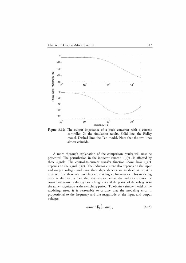
Chapter 3. Current-Mode Control 113
Figure 3.12: The output impedance of a buck converter with a current controller. X: the simulation results. Solid line: the Ridley model. Dashed line: the Tan model. Note that the two lines almost coincide.
A more thorough explanation of the comparison results will now be
presented. The perturbation in the inductor current, )(ˆ tiL , is affected by three signals. The control-to-current transfer function shows how )(ˆ tiL depends on the signal )(ˆ tic . The inductor current also depends on the input and output voltages and since these dependencies are modeled at dc, it is expected that there is a modeling error at higher frequencies. This modeling error is due to the fact that the voltage across the inductor cannot be considered constant during a switching period if the period of the voltage is in the same magnitude as the switching period. To obtain a simple model of the modeling error, it is reasonable to assume that the modeling error is proportional to the frequency and the magnitude of the input and output voltages:
( ) ,ˆ~ˆin error oL vi ω (3.74)
101
102
103
104
-40
-30
-20
-10
0
101
102
103
104
-80
-60
-40
-20
0
Frequency (Hz)
Pha
se (
deg)
; M
agni
tude
(dB
)
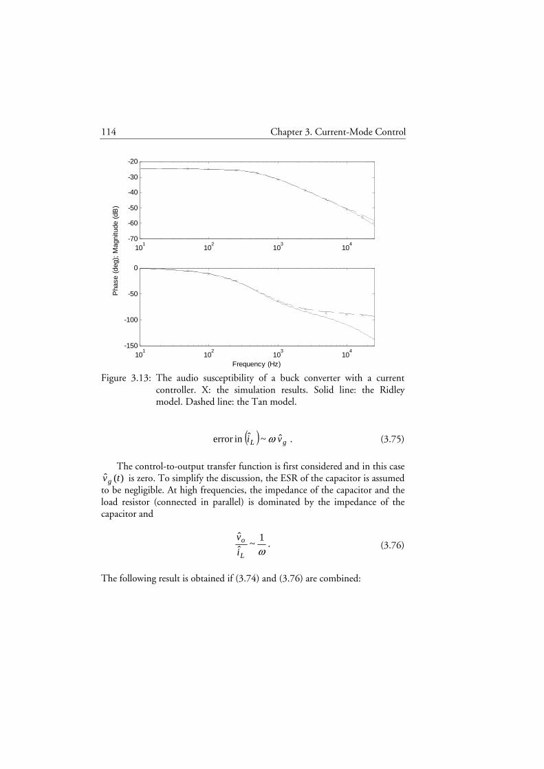
114 Chapter 3. Current-Mode Control
Figure 3.13: The audio susceptibility of a buck converter with a current controller. X: the simulation results. Solid line: the Ridley model. Dashed line: the Tan model.
( ) .ˆ~ˆin error gL vi ω (3.75)
The control-to-output transfer function is first considered and in this case )(ˆ tvg is zero. To simplify the discussion, the ESR of the capacitor is assumed
to be negligible. At high frequencies, the impedance of the capacitor and the load resistor (connected in parallel) is dominated by the impedance of the capacitor and
.1
~ˆˆ
ωL
o
i
v (3.76)
The following result is obtained if (3.74) and (3.76) are combined:
101
102
103
104
-70
-60
-50
-40
-30
-20
101
102
103
104
-150
-100
-50
0
Frequency (Hz)
Pha
se (
deg)
; M
agni
tude
(dB
)
Chapter 3. Current-Mode Control 115
( ) .ˆ~ˆ1~ˆ~ˆin error LLoL iivi
ωωω (3.77)
From (3.77), it is seen that the relative error in )(ˆ tiL is independent of
the frequency. The relative error in )(ˆ tvo is proportional to the relative error in )(ˆ tiL . The conclusion is that there is no significant increase in the relative error in )(ˆ tvo when the frequency of )(ˆ tic is increased.
The output impedances are now considered and in this case )(ˆ tvg and )(ˆ tic are zero. The perturbation of the total current, )(ˆ titotal , to the output
stage is the sum of )(ˆ tiL and )(ˆ tiinj− . The corresponding result of (3.76) is:
.1
~ˆˆ
ωtotal
o
i
v (3.78)
Assume that )(ˆ tiinj has constant amplitude and that the frequency increases. The changes in the output voltage then decrease according to (3.78). Since
)(ˆ tvg and )(ˆ tic are zero, the changes in the inductor current depends only on the changes in the output voltage. Therefore, the changes in the inductor current decrease and the fraction injL ii ˆˆ also decreases. )(ˆ titotal is more and more dominated by )(ˆ tiinj and the relative error in )(ˆ titotal does not increase even if the relative error in )(ˆ tiL increases.
Finally, the audio susceptibility is considered and now )(ˆ tic is zero. From Figure 3.13, it is seen that the audio susceptibility can be approximated by a first order system. This means that the amplitude of )(ˆ tiL is almost the same for all shown frequencies if the amplitude of the input voltage is constant. Assume that the changes in the input voltage have constant amplitude and that the frequency increases. From (3.75), it is apparent that the error in
)(ˆ tiL increases. Therefore, the relative error in )(ˆ tiL also increases. Consequently, the relative error in )(ˆ tvo increases when the frequency of
)(ˆ tvg increases.
3.6 The Ridley Model Applied to the Boost Converter
In this section, the Ridley model is used to obtain the control-to-output transfer function, the output impedance, and the audio susceptibility for the boost converter with current-mode control. These transfer function are also compared with simulation results.

116 Chapter 3. Current-Mode Control
Transfer Functions
In Section 3.4 we derived general expressions for the control-to-output transfer function, the output impedance, and the audio susceptibility. In this subsection, these expressions are used to derive the transfer functions for the boost converter with current-mode control according to the Ridley model. The methodology is analogous to the buck converter modeling.
For the boost converter, (3.43) is modified by using (2.135) and (2.142):

Chapter 3. Current-Mode Control 117
( ) ( )( )( )
( )
( ) ( )( )( )
( )( )( )( )
( ) ( )
( )( )( )
( )( )( )( )(
( )( )( )( ) ( )( ))
( ) ( )
( ) ( )
( )
( ) ( ),
)('
11'
'
'
'
'2)(
1'
1'
)(')(1
'1'
''')(
1'
)('')(
1'
1'
'
'1'
)(
1'
)('')(
1'''
'
'1
')(
1'''
)()(
)(ˆ)(ˆ
22
1
22
1
22
1
22
11
22
1
22
22
11
1
22
22
1
sdenDR
LRRsCsRRD
RD
RRDCRRs
RD
RRDsH
CsRDR
LRRsRD
R
k
V
sden
R
RRD
R
sFCsR
DR
LRRsRD
RRDCRRsRDRRDRsH
CsRLRRsDRk
sdenVDRRDsF
CsRLRRsDRR
CsRLRRsDR
CRRsRRD
RDRRD
RsH
kCsRLRRsDR
sdenVDRRDsFR
CsRLRRsDRDRRD
V
CRRsRRD
RD
D
V
RsHk
CsRLRRsDRDRRD
Vsden
sFRsi
sv
cc
cc
ce
cc
i
r
g
olc
i
mc
c
cccie
ccr
olgcm
cci
cc
cc
c
ie
rcc
olgcmi
ccc
g
cc
g
ier
ccc
g
olmi
c
o
+−+
=
+++
+
++
+−
−
+•+
+−
=+++++
+++−
−+
•++−
=
++−
++
+++
+−
++−
+
=
++−+
++
++
+
−++−
+
=
−
−
−
−−
−
−−
−
−
(3.79)
118 Chapter 3. Current-Mode Control
where
( ) ( ) ( ) ( )( ) ( )( ) ( )( ) ,1''
'''
)(2
CRRssLCsRRRRRDRD
LCRRsCDRRLsRRRRDRD
sden
cccc
cccc
ol
++++++=++++++
=
(3.80)
( )( ) ( ) ( )( )
( ) ( ) ( ) ( ) ( )( ) .''''2)(
'11'
')()()(
221
111
RDRRDCRRsRDRRDsH
DRLRRsCsRRDkR
RRRDsdenVsFRsden
ccce
ccri
colgmi
++++++−+
−+=−
−−−
(3.81)
)(sdenol is the denominator in the open loop transfer functions and )(sden
is the denominator in the closed loop transfer functions. For the boost converter, (3.44) is rewritten by using (2.135), (2.137), (2.142), and (2.143):

Chapter 3. Current-Mode Control 119
( ) ( )
( )( )
( )
( )
( ) ( )
( ) ( )
.)('
1')('
1'
1'
'1'
)(
1
)(
1
)(
1'
)(
1')(
)(
1'
)('
11'
)(ˆ)(ˆ
)(
22
221
2
2
221
+
+
++
+−
++
+
+
+−
•+
=
+
+
+
+
++
+
+
+
•
+−+
=−=
−
−
sdensLRR
DDRR
CsRRDsHDR
LRRsD
CsRRsLRR
DDRRk
DR
LRRsDR
sdensden
CsRR
sden
CsRsRLRR
DDRR
sden
CsRRDRsH
sden
CsRsRLRR
DDRR
k
sdenDR
LRRsCsRRDR
si
svsZ
c
c
cec
cc
cr
ci
ol
c
ol
cc
c
ol
cie
ol
cc
c
r
cci
inj
oout
(3.82)
For the boost converter, (3.45) is rewritten by using (2.135), (2.139), (2.142), and (2.144):
120 Chapter 3. Current-Mode Control
( ) ( )
( ) ( )
( )
( ) ( )
( ) ( )
( ) ( )( ) .)('1)('
1'
1''
1'
)('
1')(
1
)(
1
)(
1'
)(
1)(
)(
1'
)('
11'
)(ˆ
)(ˆ
22
221
221
221
+++
+−
−+
+−
+
+−
+
=+
+
++−
++
•
+−+
=
−
−
−
sdenDCRRssHDR
LRRsD
CsRRDkDR
LRRsDR
sdenkDR
LRRsDR
sdensden
CsRR
sden
CsRRD
sden
CRRsRsH
sden
CsRRDkk
sdenDR
LRRsCsRRDR
sv
sv
cec
crc
i
olfc
iol
c
ol
c
ol
cie
ol
crf
cci
g
o
(3.83)
Ridley (1990a) presents the following model for the boost converter:
,2L
RTk is
f −= (3.84)
,2
'2
L
RTDk is
r = (3.85)
)(sFm is defined in (3.32), and )(sH e is defined in (3.35).
For the boost converter, the slope of the inductor current while the transistor is on is
.1 L
VM
g= (3.86)
The first term in (3.81) is rewritten by using (3.32), (3.29), (3.86), and (3.80):
Chapter 3. Current-Mode Control 121
( )( )
( )
( )( ) .1'
''
')(
')(
')(
')()(
11
1
11
111
+++
+
+++
=+
=+
=+
=+
−−
−−
−−−
CRRssLCsRRR
RRDRD
R
RRD
L
mT
R
RRDsden
V
T
L
Vm
RRRDsdenVTMRmR
RRRDsdenVTSmR
RRRDsdenVsFR
ccc
cccs
col
g
sgc
colgsici
colgsnci
colgmi
(3.87)
(3.81) is rewritten by using (3.87) and (3.85):
( )( )
( ) ( )
( ) .'
'
'
'2)(
'11
2
'
1'
''
)(
22
3
+++
+
+
+−+
−
+++
+
+++
=
RD
RRDCRRs
RD
RRDsH
DR
LRRsCsR
L
TRD
CRRssLCsRRR
RRDRD
R
RRD
L
mT
sden
cc
ce
cc
s
ccc
cccs
(3.88)
The large parenthesis in (3.82) is rewritten by using (3.85), (3.88), (3.35)
and (3.80):
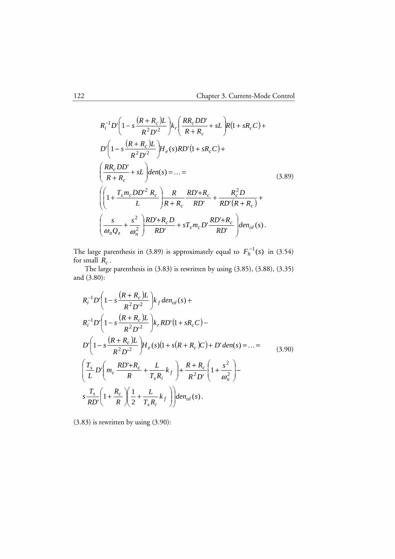
122 Chapter 3. Current-Mode Control
( ) ( )
( ) ( )
( )
.)('
''
'
'
''
''1
)('
1')('
1'
1'
'1'
2
2
22
22
221
sdenRD
RRDDmsT
RD
DRRDs
Q
s
RRRD
DR
RD
RRD
RR
R
L
RDDmT
sdensLRR
DDRR
CsRRDsHDR
LRRsD
CsRRsLRR
DDRRk
DR
LRRsDR
olc
csc
nzn
c
cc
c
ccs
c
c
cec
cc
cr
ci
++
+
+
+
++
++
+
==
+
+
++
+−
++
+
+
+−−
ωω
K (3.89)
The large parenthesis in (3.89) is approximately equal to )(1 sFh
− in (3.54) for small cR .
The large parenthesis in (3.83) is rewritten by using (3.85), (3.88), (3.35) and (3.80):
( )
( ) ( )
( ) ( )( )
.)(2
11
'
1'
''
)('1)('
1'
1''
1'
)('
1'
2
2
2
22
221
221
sdenkRT
L
R
R
RD
Ts
s
DR
RRk
RT
L
R
RRDmD
L
T
sdenDCRRssHDR
LRRsD
CsRRDkDR
LRRsDR
sdenkDR
LRRsDR
olfis
cs
n
cf
is
cc
s
cec
crc
i
olfc
i
+
+
−
+
++
+
+
==+++
+−
−+
+−
+
+−
−
−
ω
K (3.90)
(3.83) is rewritten by using (3.90):
Chapter 3. Current-Mode Control 123
( ).
)(
1
2
11
'
1'
''
)(ˆ
)(ˆ2
2
sden
CsRk
RT
L
R
R
D
Ts
s
RD
RRk
RT
L
R
RRDmD
L
RT
sv
sv
cf
is
cs
n
cf
is
cc
s
g
o
+
+
+
−
+
++
+
+=
ω (3.91)
The transfer functions obtained by applying the Ridley model to the
boost converter are now summarized. The denominators are the same and given by (3.88). The control-to-output transfer function of the closed loop system is given directly by (3.79). The output impedance of the closed loop system is obtained by combining (3.82) and (3.89). The audio susceptibility of the closed loop system is obtained by combining (3.91) and (3.84). The results are:
( ) ( )
,)(
'11'
)(ˆ
)(ˆ
)(ˆ)(ˆ 22
sdenDR
LRRsCsRRD
Rsv
sv
si
svc
c
ic
o
c
o
+−+
== (3.92)
( )
( )
,'
''
'
'
''
''1
)(
1)(
2
2
22
++
+
+
+
++
++
+
•+
=
RD
RRDDmsT
RD
DRRDs
Q
s
RRRD
DR
RD
RRD
RR
R
L
RDDmT
sden
CsRRsZ
ccs
c
nzn
c
cc
c
ccs
cout
ωω
(3.93)
( ),
)(
11'
5.0'
'
)(ˆ
)(ˆ
2
2
sden
CsRs
RD
RR
R
RRDmD
L
RT
sv
sv
cn
ccc
s
g
o
+
+
++
−+
=
ω
(3.94)
where

124 Chapter 3. Current-Mode Control
( )( )
( ) ( )
( ) ,'
'
'
'2)(
'11
2
'
1'
''
)(
22
3
+++
+
+
+−+
−
+++
+
+++
=
RD
RRDCRRs
RD
RRDsH
DR
LRRsCsR
L
TRD
CRRssLCsRRR
RRDRD
R
RRD
L
mT
sden
cc
ce
cc
s
ccc
cccs
(3.95)
and )(sHe is defined in (3.35).
Simulation Results
In this section, a simulation model of a boost converter with current-mode control is presented. The transfer functions derived in the previous subsection are compared with simulation results.
The simulation model shown in Figure 3.9 is used, except the buck converter subsystem is replaced with the boost converter subsystem shown in Figure 2.14. The parameters used in the simulation model presented in Section 2.7 are also used here. Ic is adjusted manually so that the average value of the output voltage, oV , is equal to 8 V ( D =0.382). eM is calculated by using (3.21) and (3.86):
( ) ,1−= cg
e mL
VM (3.96)
where cm is chosen to be 2.
Figure 3.14 shows the Bode plot for the control-to-output transfer function in (3.92) together with the simulation results. iR is set to 1 Ω. From the figure it is seen that the control-to-output transfer function predicted by the Ridley model agrees closely with the simulation results.
Figure 3.15 shows the Bode plot for the output impedance in (3.93) together with the simulation results. From the figure it is seen that the output impedance predicted by the Ridley model agrees closely with the simulation results.
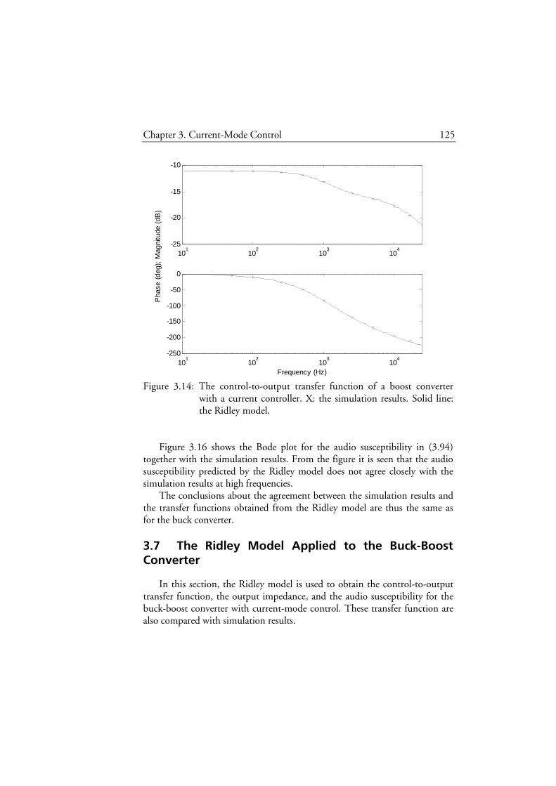
Chapter 3. Current-Mode Control 125
Figure 3.14: The control-to-output transfer function of a boost converter with a current controller. X: the simulation results. Solid line: the Ridley model.
Figure 3.16 shows the Bode plot for the audio susceptibility in (3.94)
together with the simulation results. From the figure it is seen that the audio susceptibility predicted by the Ridley model does not agree closely with the simulation results at high frequencies.
The conclusions about the agreement between the simulation results and the transfer functions obtained from the Ridley model are thus the same as for the buck converter.
3.7 The Ridley Model Applied to the Buck-Boost Converter
In this section, the Ridley model is used to obtain the control-to-output transfer function, the output impedance, and the audio susceptibility for the buck-boost converter with current-mode control. These transfer function are also compared with simulation results.
101
102
103
104
-25
-20
-15
-10
101
102
103
104
-250
-200
-150
-100
-50
0
Frequency (Hz)
Pha
se (
deg)
; M
agni
tude
(dB
)
126 Chapter 3. Current-Mode Control
Figure 3.15: The output impedance of a boost converter with a current controller. X: the simulation results. Solid line: the Ridley model.
Transfer Functions
In Section 3.4 we derived general expressions for the control-to-output transfer function, the output impedance, and the audio susceptibility. In this subsection, these expressions are used to derive the transfer functions for the buck-boost converter with current-mode control according to the Ridley model. The methodology is analogous to the modeling of the buck and boost converters.
For the buck-boost converter, (3.43) is rewritten by using (2.179) and (2.186):
101
102
103
104
-40
-30
-20
-10
0
101
102
103
104
-80
-60
-40
-20
0
Frequency (Hz)
Pha
se (
deg)
; M
agni
tude
(dB
)
Chapter 3. Current-Mode Control 127
( )( ) ( )( )
( )
( )( ) ( )( )
( )( )( )( )
( ) ( )
( )( )( )
( )( )( )( )(
( )( )( )( ) ( )( ))
( )
( )
( )
( ),
)('
11'
'
'
'
'')(
1'
1'
)(')(1
'1'
''')(
1'
)('')(
1'
1'
'
'1'
)(
1'
)('')(
1'''
'
'1
')(
1'''
)()(
)(ˆ)(ˆ
2
1
2
1
2
1
2
11
2
1
2
2
11
1
2
2
1
sdenRD
LDsCsRRD
D
RRDsC
DRR
RRDDRDsH
CsRRD
LDsRD
R
k
V
sden
RR
RRD
R
sFCsR
RD
LDsRD
RRDCRRsRDDRRDRsH
CsRsLDRDRRk
sdenVDRRDsF
CsRsLDRDRRR
CsRsLDRDRR
CRRsRRD
RDDRRD
RsH
kCsRsLDRDRR
sdenVDRRDsFR
CsRsLDRDDRRD
RRV
CRRsRRD
RDD
D
V
RsHk
CsRsLDRDDRRD
RRV
sdensFR
si
sv
c
c
c
ce
ci
r
g
ol
c
c
i
mc
cccie
ccr
olgcm
cci
cc
cc
c
ie
rcc
olgcmi
cc
cg
cc
g
ier
cc
cg
olmi
c
o
−+
=
++
+++
++
−
−
++
+
−
=+++++
++−+
−+
•+−+
=
+−+
++
+++
+−
+−+
+
=
+−+
+
++
++
+
−+−
++
=
−
−
−
−−
−
−−
−
−
(3.97)
128 Chapter 3. Current-Mode Control
Figure 3.16: The audio susceptibility of a boost converter with a current controller. X: the simulation results. Solid line: the Ridley model.
where
( ) ( ) ( ) ( )( ) ( )( ) ( )( ) ,1''
'''
)(2
CRRssLCsRRRRRDRD
LCRRsCDRRLsRRRRDRD
sden
cccc
cccc
ol
++++++=++++++
=
(3.98)
( ) ( )( ) ( )( )
( )( ) ( )( ) ( )( ) .'''1')(
'11'
')()()(
21
111
DRRDsCDRRRDRDsH
RDsLDCsRRDkR
RRRRDsdenVsFRsden
ccce
cri
ccolgmi
++++++−+
−++=−
−−−
(3.99)
)(sdenol is the denominator in the open loop transfer functions and )(sden
is the denominator in the closed loop transfer functions. For the buck-boost converter, (3.44) is rewritten by using (2.179), (2.181), (2.186), and (2.187):
101
102
103
104
-60
-40
-20
0
101
102
103
104
-150
-100
-50
0
Frequency (Hz)
Pha
se (
deg)
; M
agni
tude
(dB
)

Chapter 3. Current-Mode Control 129
( )
( )( )
( )
( )
( )
( )
.)('
1')('
1'
1'
'1'
)(
1
)(
1
)(
1'
)(
1')(
)(
1'
)('
11'
)(ˆ)(ˆ
)(
2
21
2
2
21
+
+
++
−
++
+
+
−
•+
=
+
+
+
+
++
+
+
+
•
−+=−=
−
−
sdensLRR
DDRR
CsRRDsHRD
LDsD
CsRRsLRR
DDRRk
RD
LDsDR
sdensden
CsRR
sden
CsRsRLRR
DDRR
sden
CsRRDRsH
sden
CsRsRLRR
DDRR
k
sdenRD
LDsCsRRDR
si
svsZ
c
c
ce
cc
cri
ol
c
ol
cc
c
ol
cie
ol
cc
c
r
ci
inj
oout
(3.100)
For the buck-boost converter, (3.45) is rewritten by using (2.179), (2.183), (2.186), and (2.188):
130 Chapter 3. Current-Mode Control
( )
( ) ( )( )
( )
( )
( )
( )( ) .)('1)('
1'
1''
1'
)('
1')(
1
)(
1
)(
1'
)(
1)(
)(
1'
)('
11'
)(ˆ
)(ˆ
2
21
21
21
+++
−
−+
−
+
−+
=+
+
++−
++
•
−+=
−
−
−
sdenDDCRRsDsHRD
LDsD
CsRRDDkRD
LDsDR
sdenkRD
LDsDR
sdensden
CsRR
sden
CsRRDD
sden
CRRsDRsH
sden
CsRRDDkk
sdenRD
LDsCsRRDR
sv
sv
ce
cri
olfiol
c
ol
c
ol
cie
ol
crf
ci
g
o
(3.101)
Ridley (1990a) presents the following model for the buck-boost
converter:
,2
1
−−= D
L
RDTk is
f (3.102)
,2
'2
L
RTDk is
r = (3.103)
)(sFm is defined in (3.32), and )(sH e is defined in (3.35).
For the buck-boost converter, the slope of the inductor current while the transistor is on is
.1 L
VM
g= (3.104)
The first term in (3.99) is rewritten by using (3.32), (3.29), (3.104), and (3.98):

Chapter 3. Current-Mode Control 131
( ) ( )( ) ( )
( ) ( )
( )( ) .1'
''
')(
')(
')(
')()(
11
1
11
111
+++
+
++
++
=++
=++
=++
=++
−−
−−
−−−
CRRssLCsRRR
RRDRD
RR
RRD
L
mT
RR
RRDsden
V
T
L
Vm
RRRRDsdenVTMRmR
RRRRDsdenVTSmR
RRRRDsdenVsFR
ccc
c
c
ccs
c
col
g
sgc
ccolgsici
ccolgsnci
ccolgmi
(3.105)
(3.99) is rewritten by using (3.105) and (3.103):
( )( )
( )
( )( ) .
'
'
'
1')(
'11
2
'
1'
''
)(
2
3
++
+++
+
−+
−
+++
+
++
++
=
D
RRDsC
DRR
RDRDsH
RD
LDsCsR
L
TRD
CRRssLCsRRR
RRDRD
RR
RRD
L
mT
sden
c
c
ce
cs
ccc
c
c
ccs
(3.106)
The large parenthesis in (3.100) is rewritten by using (3.103), (3.106),
(3.35) and (3.98):
132 Chapter 3. Current-Mode Control
( )
( )
( )( )
( )( ) ( )
( )( ) ( ) .)(
'
''
'
'1'
'
'''
)('
1')('
1'
1'
'1'
2
2
22
2
2
21
sdenDRR
RRDDmsT
DRR
DDRRDs
Q
s
DRR
R
RRL
RRDRRDDmT
RR
DRDRRR
sdensLRR
DDRR
CsRRDsHRD
LDsD
CsRRsLRR
DDRRk
RD
LDsDR
olc
ccs
c
c
nzn
c
c
c
cccs
c
cc
c
c
ce
cc
cri
+
++
+−+
+
+
++
+
++
+
−+
==
+
+
++
−
++
+
+
−−
ωω
K (3.107)
The large parenthesis in (3.107) is approximately equal to )(1 sFh
− in (3.54) for small cR .
The large parenthesis in (3.101) is rewritten by using (3.103), (3.106), (3.35) and (3.98):
( )
( )( )
.)(2'
1'
''
)('1)('
1'
1''
1'
)('
1'
2
2
2
21
21
sDdenkRT
LD
RD
Ts
s
RD
Dk
RDT
L
RR
RRDmD
L
T
sdenDDCRRsDsHRD
LDsD
CsRRDDkRD
LDsDR
sdenkRD
LDsDR
olfis
s
nf
isc
cc
s
ce
cri
olfi
+
−
++
+
++
==+++
−
−+
−
+
−
−
−
ω
K (3.108)
(3.101) is rewritten by using (3.108):
Chapter 3. Current-Mode Control 133
( ).
)(
1
2'
1'
''
)(ˆ
)(ˆ2
2
sden
CsRDk
RT
LD
D
Ts
s
D
Dk
RDT
L
RR
RRDmD
L
RT
sv
sv
cf
is
s
nf
isc
cc
s
g
o
+
+
−
++
+
++
=ω
(3.109)
The transfer functions obtained by applying the Ridley model to the
buck-boost converter are now summarized. The denominators are the same and given by (3.106). The control-to-output transfer function of the closed loop system is given directly by (3.97). The output impedance of the closed loop system is obtained by combining (3.100) and (3.107). The audio susceptibility of the closed loop system is obtained by combining (3.109) and (3.102). The results are:
( )
,)(
'11'
)(ˆ
)(ˆ
)(ˆ)(ˆ 2
sdenRD
LDsCsRRD
Rsv
sv
si
sv c
ic
o
c
o
−+==
(3.110)
( )
( )( )
( )( ) ( )
( )( ) ( ) ,
'
''
'
'1'
'
'''
)(
1)(
2
2
22
2
+
++
+−+
+
+
++
+
++
+
−+
•+
=
DRR
RRDDmsT
DRR
DDRRDs
Q
s
DRR
R
RRL
RRDRRDDmT
RR
DRDRRR
sden
CsRRsZ
c
ccs
c
c
nzn
c
c
c
cccs
c
cc
cout
ωω
(3.111)
134 Chapter 3. Current-Mode Control
( )
( ),
)(
1
2
1'2
1'
'
)(
1
21
2'
1'2
1'
')(ˆ
)(ˆ
2
2
2
2
sden
CsRDDTs
s
D
DD
RR
RRDmD
L
RT
sden
CsRDDD
D
D
Ts
s
D
DD
RR
RRDmD
L
RT
sv
sv
cs
nc
cc
s
cs
nc
cc
s
g
o
+
+
++
−−
++
=+
−−
−
++
−−
++
=
ω
ω
(3.112)
where
( )( )
( )
( )( ) .
'
'
'
1')(
'11
2
'
1'
''
)(
2
3
++
+++
+
−+
−
+++
+
++
++
=
D
RRDsC
DRR
RDRDsH
RD
LDsCsR
L
TRD
CRRssLCsRRR
RRDRD
RR
RRD
L
mT
sden
c
c
ce
cs
ccc
c
c
ccs
(3.113)
and )(sHe is defined in (3.35).
Simulation Results
In this section, a simulation model of a buck-boost converter with current-mode control is presented. The transfer functions derived in the previous subsection are compared with simulation results.
The simulation model shown in Figure 3.9 is used, except the buck converter subsystem is replaced with the buck-boost converter subsystem shown in Figure 2.20. The parameters used in the simulation model presented in Section 2.10 are also used here. Ic is adjusted manually so that the average value of the output voltage, oV , is equal to 8 V ( D =0.620). eM is calculate by using (3.21) and (3.104):
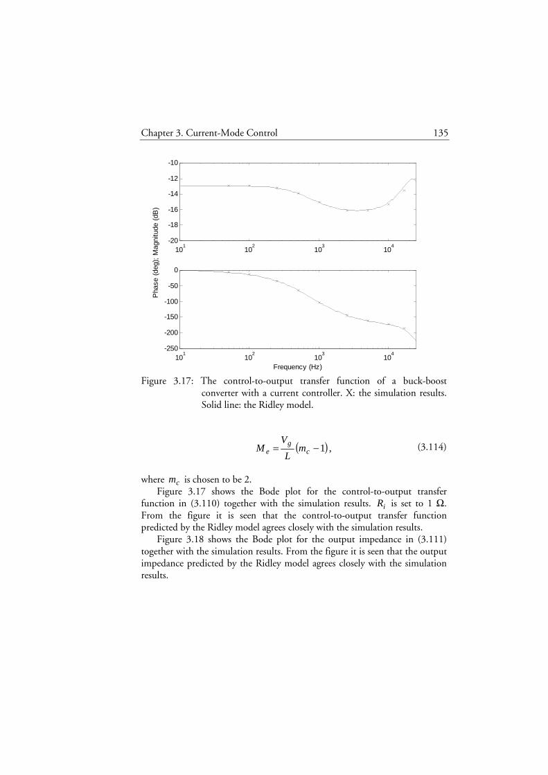
Chapter 3. Current-Mode Control 135
Figure 3.17: The control-to-output transfer function of a buck-boost converter with a current controller. X: the simulation results. Solid line: the Ridley model.
( ) ,1−= cg
e mL
VM (3.114)
where cm is chosen to be 2.
Figure 3.17 shows the Bode plot for the control-to-output transfer function in (3.110) together with the simulation results. iR is set to 1 Ω. From the figure it is seen that the control-to-output transfer function predicted by the Ridley model agrees closely with the simulation results.
Figure 3.18 shows the Bode plot for the output impedance in (3.111) together with the simulation results. From the figure it is seen that the output impedance predicted by the Ridley model agrees closely with the simulation results.
101
102
103
104
-20
-18
-16
-14
-12
-10
101
102
103
104
-250
-200
-150
-100
-50
0
Frequency (Hz)
Pha
se (
deg)
; M
agni
tude
(dB
)
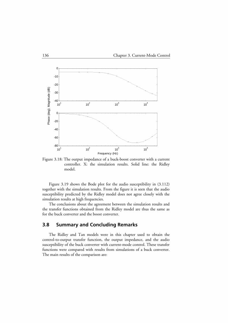
136 Chapter 3. Current-Mode Control
Figure 3.18: The output impedance of a buck-boost converter with a current controller. X: the simulation results. Solid line: the Ridley model.
Figure 3.19 shows the Bode plot for the audio susceptibility in (3.112)
together with the simulation results. From the figure it is seen that the audio susceptibility predicted by the Ridley model does not agree closely with the simulation results at high frequencies.
The conclusions about the agreement between the simulation results and the transfer functions obtained from the Ridley model are thus the same as for the buck converter and the boost converter.
3.8 Summary and Concluding Remarks
The Ridley and Tan models were in this chapter used to obtain the control-to-output transfer function, the output impedance, and the audio susceptibility of the buck converter with current-mode control. These transfer functions were compared with results from simulations of a buck converter. The main results of the comparison are:
101
102
103
104
-40
-30
-20
-10
0
101
102
103
104
-80
-60
-40
-20
0
Frequency (Hz)
Pha
se (
deg)
; M
agni
tude
(dB
)

Chapter 3. Current-Mode Control 137
Figure 3.19: The audio susceptibility of a buck-boost converter with a current controller. X: the simulation results. Solid line: the Ridley model.
• The control-to-output transfer functions predicted by the Ridley and
Tan models are almost the same and they agree closely with the simulation results.
• The output impedances predicted by the Ridley and Tan models are almost the same and they agree closely with the simulation results.
• The audio susceptibilities predicted by the Ridley and Tan models are not the same and neither agrees closely with the simulation results at high frequencies.
The reason why the control-to-output transfer functions and the output impedances are so accurate at high frequencies is that the perturbation in the output voltage is small at high frequencies. In the case where the audio susceptibility is considered, the perturbation in the input voltage is not small at high frequencies while the frequency function is evaluated.
In this chapter, the Ridley model was also used to obtain the transfer functions for the boost and buck-boost converters with current-mode control.
101
102
103
104
-40
-30
-20
-10
0
101
102
103
104
-80
-60
-40
-20
0
Frequency (Hz)
Pha
se (
deg)
; M
agni
tude
(dB
)

138 Chapter 3. Current-Mode Control
These transfer function were compared with results from simulations. The result of this comparison is that the audio susceptibilities predicted by the Ridley model do not agree closely with the simulation results at high frequencies, i.e. the same result as was obtained for the buck converter.

139
Chapter 4 A Novel Model
Models for converters with current-mode control were considered in Chapter 3. We showed that the way the changes in the input and output voltages are treated in the Ridley and Tan models introduces a modeling error at high frequencies. We also showed that this modeling error is significant for the audio susceptibility. To obtain an accurate model for the audio susceptibility, the changes in the input and output voltages must be treated in a more refined way. In this chapter, a novel model for the audio susceptibility is derived and compared with simulation results. This model will be utilized in Chapter 5 to improve the Ridley and Tan models.
4.1 Chapter Survey
A novel model for the audio susceptibility is derived in Section 4.2. In Section 4.3, this model is applied to the buck converter and the result is compared with simulation results and the Ridley and Tan models. In Section 4.4, the novel model is applied to the boost converter and the result is compared with simulation results and the Ridley model. The corresponding work is made for the buck-boost converter in Section 4.5. A summary and concluding remarks are presented in Section 4.6.
4.2 A Novel Model for the Audio Susceptibility
In this section, a novel model for the audio susceptibility is derived. It is first shown that it is easy to obtain a model if the perturbation in the duty cycle, )(ˆ sd , is known. As an intermediate step, a model for )(ˆ zd is derived. To be able to motivate that the novel model is reasonable, the spectrum of
)(ˆ nd and )(ˆ tvo are examined. Finally, the novel model is presented.

140 Chapter 4. A Novel Model
Introduction
The audio susceptibility describes how a perturbation in the input voltage affects the output voltage. Figure 4.1 shows the converter and the current controller. In the case where the audio susceptibility is considered, the reference signal, )(tic , is constant and the input voltage, )(tvg , is perturbed. If the current controller is not present, a perturbation in )(tvg causes a perturbation in the output voltage and the inductor current according to the transfer functions
,)(ˆ
)(ˆ
olg
o
sv
sv
(4.1)
,)(ˆ
)(ˆ
olg
L
sv
si
(4.2)
which were derived for the buck, boost, and buck-boost converters in Chapter 2. In the case where the current controller is present, a perturbation in )(tvg causes a perturbation in the duty cycle of )(tδ since the inductor current is fed back to the current controller. The perturbation in the duty cycle of )(tδ causes a perturbation in the output voltage and the inductor current according to the transfer functions
,)(ˆ)(ˆ
sd
svo (4.3)
,)(ˆ)(ˆ
sd
siL (4.4)
that were derived in Chapter 2. Since the rule of superposition holds for the linearized converter, the Laplace transform of the perturbed output voltage is
.)(ˆ)(ˆ)(ˆ
)(ˆ)(ˆ
)(ˆ)(ˆ sd
sd
svsv
sv
svsv o
g
olg
oo +
= (4.5)

Chapter 4. A Novel Model 141
Figure 4.1: The converter and the current controller.
If )(ˆ sd were known, )(ˆ svo could be calculated with (4.5). A model for )(ˆ zd (the Z-transform of the sampled version of )(ˆ td ) will first be derived.
A Model for )(zd
In this subsection, a model for )(ˆ zd is derived. A model for the discrete-time signal )(ˆ nd is first derived by considering the perturbations in the slopes of the inductor current. The result is then transformed to the frequency domain.
The voltage across the inductor depends on the input and output voltages and the topology of the converter according to Table 4.1, see Chapter 2 or Ridley (1990b, Table 4.2). The positive voltage across the inductor as the transistor is on is called )(tvon while the positive voltage across the inductor as the transistor is off is called )(tvoff . Both these voltages are here defined to be equal to the expressions in Table 4.1 for all t , i.e. the expressions for
)(tvon is valid also when the transistor is off and the expressions for )(tvoff is valid also when the transistor is on.
Table 4.1: The positive voltage across the inductor.
Buck Boost Buck-Boost
)(tvon )()( tvtv og − )(tvg )(tvg
)(tvoff )(tvo )()( tvtv go − )(tvo
vg(t)
Currentcontroller
vo(t)
ic(t) δ (t) iL(t) Converter

142 Chapter 4. A Novel Model
The slopes of the inductor current are calculated by:
( ) ,)(1
)(ˆ1
)(ˆ)( 111 tvL
tvVL
tmMtm ononon =+=+= (4.6)
( ) .)(1
)(ˆ1
)(ˆ)( 222 tvL
tvVL
tmMtm offoffoff =+=+= (4.7)
)(1 tm is the positive slope of the inductor current while the transistor is on.
Note that it is defined for all t since it is a function of )(tvon . The negative slope of the inductor current as the transistor is off corresponds to )(2 tm− . This function is also defined for all t since it is a function of )(tvoff . All of
)(1 tm , 1M , )(tvon , onV , )(2 tm , 2M , )(tvoff , and offV are positive with these definitions and )(1 tm , )(ˆ1 tm , )(tvon , )(ˆ tvon , )(2 tm , )(ˆ 2 tm , )(tvoff , and )(ˆ tvoff are defined for all t with these definitions. The perturbation signals )(ˆ1 tm and )(ˆ 2 tm are zero when there are no perturbations of the input and output voltages.
When the audio susceptibility is considered, )(tic is constant and equal to its dc value cI . Figure 4.2 shows the waveforms of cI , cI minus the external ramp, )(tie , and two different versions of the inductor current. The first version ( )(tiLss , solid line) shows how the inductor current waveform is in steady state, i.e. when there are no perturbations of the inductor current slopes )(1 tm and )(2 tm− . The dashed line shows an example of how the inductor current waveform if there are perturbations of the inductor current slopes. The transistor is assumed to turn on at the points snTt = , where n is an integer. In steady state the transistor will then turn off at the points
( ) sTDnt += . To find out how much the inductor current changes, the inductor current slopes are integrated. The following two equations are obtained from Figure 4.2:
( )( )
,)()1(ˆ)()1(ˆ1
2∫−++−
+−+=−kT
kdDkT
sesLc
s
s
dttmkdDTMkTiI (4.8)
( )( )
.)()(ˆ)()(ˆ
1∫++
++=−kdDkT
kTsesLc
s
s
dttmkdDTMkTiI (4.9)
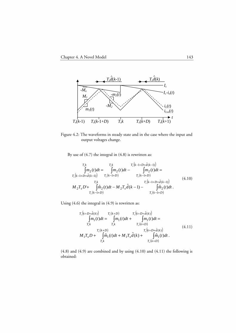
Chapter 4. A Novel Model 143
Figure 4.2: The waveforms in steady state and in the case where the input and
output voltages change. By use of (4.7) the integral in (4.8) is rewritten as:
( ) ( ) ( )
( )
( ) ( )
( ).)(ˆ)1(ˆ)(ˆ'
)()()(
)1(ˆ1
122
122
)1(ˆ1
12
12
)1(ˆ1
2
∫∫
∫∫∫
−++−
+−+−
−++−
+−+−−++−
−−−+
=−=
kdDkT
DkTs
kT
DkTs
kdDkT
DkT
kT
DkT
kT
kdDkT
s
s
s
s
s
s
s
s
s
s
dttmkdTMdttmDTM
dttmdttmdttm
(4.10)
Using (4.6) the integral in (4.9) is rewritten as:
( ) ( )
( )
( )
( )
( )
( ).)(ˆ)(ˆ)(ˆ
)()()(
)(ˆ
1111
)(ˆ
11
)(ˆ
1
∫∫
∫∫∫
++
+
+
++
+
+++
+++
=+=
kdDkT
DkTs
DkT
kTs
kdDkT
DkT
DkT
kT
kdDkT
kT
s
s
s
s
s
s
s
s
s
s
dttmkdTMdttmDTM
dttmdttmdttm
(4.11)
(4.8) and (4.9) are combined and by using (4.10) and (4.11) the following is obtained:
Ts(k+D) t
Tsk Ts(k-1+D)
iL(t)
Ic-ie(t)
Ts(k-1) Ts(k+1)
Tsd(k-1) Tsd(k)
iLss(t)
Ic
M1
-Me
-M2 m1(t)
-m2(t)
^ ^
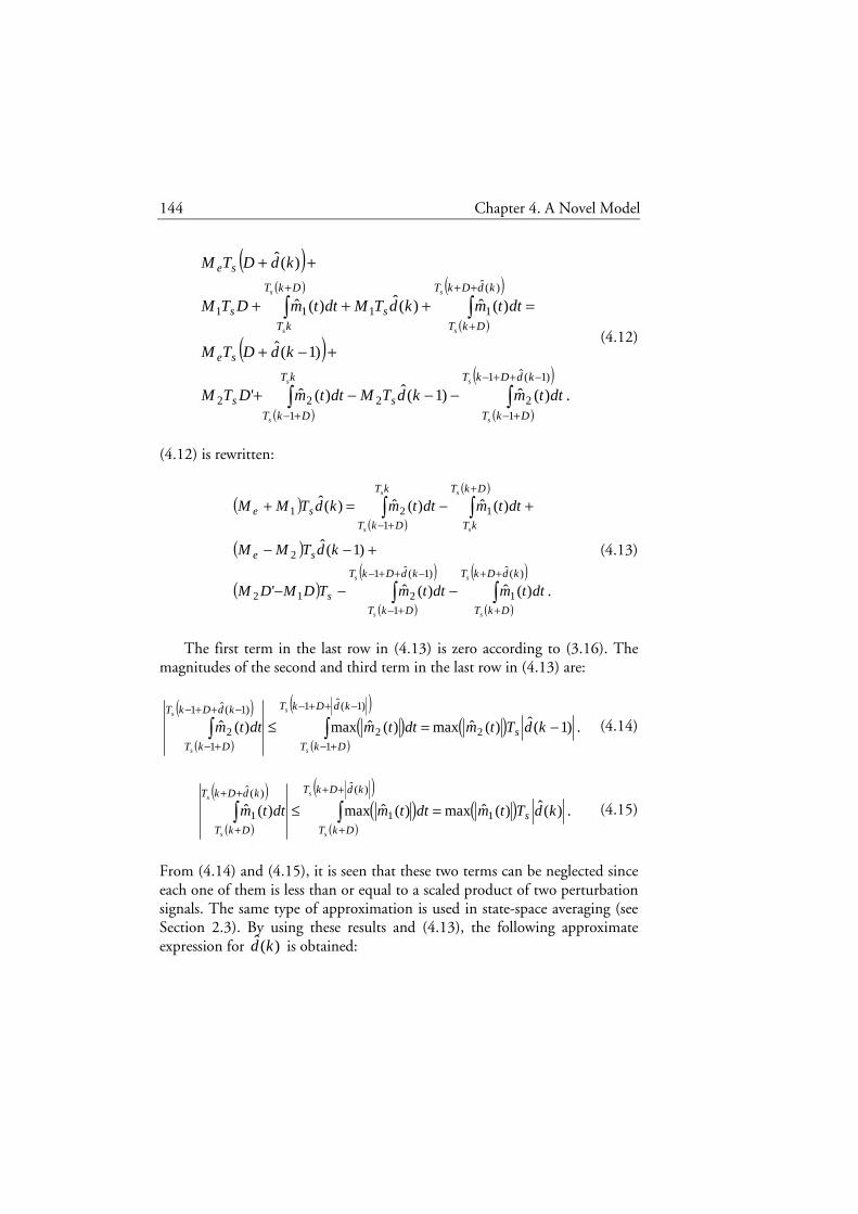
144 Chapter 4. A Novel Model
( )( )
( )
( )
( )
( ) ( )
( ).)(ˆ)1(ˆ)(ˆ'
)1(ˆ
)(ˆ)(ˆ)(ˆ
)(ˆ
)1(ˆ1
122
122
)(ˆ
1111
∫∫
∫∫
−++−
+−+−
++
+
+
−−−+
+−+
=+++
++
kdDkT
DkTs
kT
DkTs
se
kdDkT
DkTs
DkT
kTs
se
s
s
s
s
s
s
s
s
dttmkdTMdttmDTM
kdDTM
dttmkdTMdttmDTM
kdDTM
(4.12)
(4.12) is rewritten:
( )( )
( )
( )
( )( )
( )
( )
( ).)(ˆ)(ˆ'
)1(ˆ
)(ˆ)(ˆ)(ˆ
)(ˆ
1
)1(ˆ1
1212
2
11
21
∫∫
∫∫
++
+
−++−
+−
+
+−
−−−
+−−
+−=+
kdDkT
DkT
kdDkT
DkTs
se
DkT
kT
kT
DkTse
s
s
s
s
s
s
s
s
dttmdttmTDMDM
kdTMM
dttmdttmkdTMM
(4.13)
The first term in the last row in (4.13) is zero according to (3.16). The
magnitudes of the second and third term in the last row in (4.13) are:
( )
( )( ) ( )
( )
( ).)1(ˆ)(ˆmax)(ˆmax)(ˆ
)1(ˆ1
122
)1(ˆ1
12 −=≤ ∫∫
−++−
+−
−++−
+−
kdTtmdttmdttm s
kdDkT
DkT
kdDkT
DkT
s
s
s
s
(4.14)
( )
( )( ) ( )
( )
( ).)(ˆ)(ˆmax)(ˆmax)(ˆ
)(ˆ
11
)(ˆ
1 kdTtmdttmdttm s
kdDkT
DkT
kdDkT
DkT
s
s
s
s
∫∫++
+
++
+
=≤ (4.15)
From (4.14) and (4.15), it is seen that these two terms can be neglected since each one of them is less than or equal to a scaled product of two perturbation signals. The same type of approximation is used in state-space averaging (see Section 2.3). By using these results and (4.13), the following approximate expression for )(ˆ kd is obtained:

Chapter 4. A Novel Model 145
( )
( )( )
( ) .
)1(ˆ)(ˆ)(ˆ
)(ˆ1
211
2
se
se
DkT
kT
kT
DkT
TMM
kdTMMdttmdttm
kd
s
s
s
s
+
−−+−
=∫∫+
+− (4.16)
The integer variable k is substituted by the integer variable n and (4.16) can therefore be rewritten as
( ) ( )
( )( ) ( )
.)(ˆ)(ˆ)(ˆ)(ˆ1
)1(ˆ1)(ˆ
11
1
221
21
+−−
+
+−−+
=
∫∫∫∫∞−
+
∞−
+−
∞−∞−
nTDnTDnTnT
se
sese
ssss
dttmdttmdttmdttmTMM
ndTMMTMM
nd
(4.17)
The discrete-time signal )(ˆ nd is the result of sampling the continuous-
time signal )(ˆ td . The sampling interval changes if the converter is not in steady state. Similarly to the discussion in Section 3.3, sampling at the points
( ) sTDnt += is a good approximation if the magnitude of )(ˆ td is small and the changes of )(ˆ td are slow in the surroundings of these sampling points. From (4.17), it is seen that )(ˆ nd is a sum of a discrete-time part (first term) and a continuous-time part (last term). To be able to create the discrete-time signal )(ˆ nd , the continuous-time part must deliver its value at ( ) sTDnt += so that it can be sampled and added to the discrete-time part of (4.17). In the first integral in (4.17),
,)(ˆ 2∫∞−
nTs
dttm
the signal )(ˆ 2 tm is integrated up to snTt = so the value of the integral is known at snTt = . Since the value of the integral has to be delivered at
( ) sTDnt += , the value must be delayed by sDT . In the second integral in (4.17),
( )
,)(ˆ1
2∫+−
∞−
DnTs
dttm

146 Chapter 4. A Novel Model
the signal )(ˆ 2 tm should be integrated up to ( ) sTDnt +−= 1 . Since the value of the integral is to be delivered at ( ) sTDnt += , the value must be delayed by sT . In the third integral in (4.17),
( )
,)(ˆ 1∫+
∞−
DnTs
dttm
the signal )(ˆ1 tm is integrated up to ( ) sTDnt += and therefore it will not be delayed. In the fourth integral in (4.17),
,)(ˆ 1∫∞−
nTs
dttm
the signal )(ˆ1 tm is integrated up to snTt = and has to be delayed by sDT . By using these results and (4.17), the signal )(ˆ nd can be created as shown in Figure 4.3.
The block diagram in Figure 4.3 is transformed from the time domain to the frequency domain and the result is shown in Figure 4.4. A feedback is included in Figure 4.4 to eliminate one of the input signals. The feedback is transformed from the discrete-time part to the continuous-time part if z is substituted with ssTe and the result is shown in Figure 4.5.
An expression for )(ˆ sx in Figure 4.5 can be obtained from Figure 4.5:
( )( )
( ) .)(ˆ)(ˆ)(ˆ)(ˆ
)(ˆ)(ˆ
1
11
11
21
21
1
2
se
sDTsTsDT
se
sTse
TMM
smsesmssmsesmse
TMM
sxeTMMsx
sss
s
++−−
++
−=
−−−−−−−
−
(4.18)
Rearranging (4.18) gives:
( ).
)(ˆ1
)(ˆ
)(ˆ21
12
s
sss
sTee
s
sDT
s
sTsDT
eMMMM
smsT
esm
sT
ee
sx−
−−−
−−+
−+−
=(4.19)
The denominator in (4.19) is now rewritten by using (3.21) and (3.17):
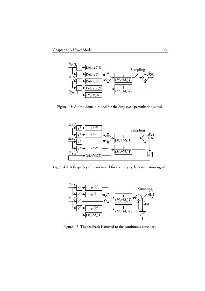
Chapter 4. A Novel Model 147
Figure 4.3: A time-domain model for the duty cycle perturbation signal.
Figure 4.4: A frequency-domain model for the duty cycle perturbation signal.
Figure 4.5. The feedback is moved to the continuous-time part.
m2(t) ^ Delay: TsD
Sampling
m1(t) ^
(Me+M1)Ts 1
(Me+M1)Ts 1
(Me-M2)Ts d(n-1) ^
∫
∫ Delay: Ts
Delay: 0 ∫
∫ Delay: TsD
d(n) ^
m2(s) ^
m1(s) ^
Sampling
(Me+M1)Ts 1
(Me+M1)Ts 1
(Me-M2)Ts d(z) ^
d(z) ^
z-1 s-1
s-1
s-1
s-1 e-sT D s
e-sT s
e-sT D s
z-1
m2(s) ^
Sampling
m1(s) ^
(Me+M1)Ts 1
(Me+M1)Ts 1
(Me-M2)Ts
d(z) ^
s-1
s-1
s-1
s-1 e-sT D s
e-sT s
e-sT D s
e-sT s
x(s) ^
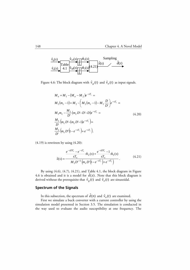
148 Chapter 4. A Novel Model
Figure 4.6: The block diagram with )(ˆ tvg and )(ˆ tvo as input signals.
( )
( ) ( )
( )
( )( )( )( ).1'
'
1'''
'''
'11
1
1
11
1111
21
ss
s
s
s
s
sTsTc
sTcc
sTcc
sTcc
sTee
eeDmD
M
eDmDmD
M
eDDDmD
MmM
eD
DMmMMmM
eMMMM
−−
−
−
−
−
+−
=−−
=−−−
=
−−−+−
=−−+
(4.20)
(4.19) is rewritten by using (4.20):
( )( ) .1''
)(ˆ1
)(ˆ
)(ˆ1
1
12
ss
sss
sTsTc
s
sDT
s
sTsDT
eeDmDM
smsT
esm
sT
ee
sx−−−
−−−
+−
−+−
= (4.21)
By using (4.6), (4.7), (4.21), and Table 4.1, the block diagram in Figure
4.6 is obtained and it is a model for )(ˆ zd . Note that this block diagram is derived without the prerequisite that )(ˆ tvg and )(ˆ tvo are sinusoidal.
Spectrum of the Signals
In this subsection, the spectrum of )(ˆ nd and )(ˆ tvo are examined. First we simulate a buck converter with a current controller by using the
simulation model presented in Section 3.5. The simulation is conducted in the way used to evaluate the audio susceptibility at one frequency. The
x(s) ^
m2(s) ^
m1(s) ^
vo(s) ^
vg(s) ^
von(s) ^
voff(s) ^ L 1
L 1
(4.21) 4.1 Table
Sampling d(z) ^

Chapter 4. A Novel Model 149
Figure 4.7: The discrete Fourier series for )(ˆ nd ( mω =5000π rad/s).
voltage )(ˆ tvg is thus sinusoidal. The simulation is conducted for the frequency 2500 Hz ( mω =5000π rad/s). We record the signal delta during the simulation. From this result the duty cycle, )(nd , of the signal delta is manually measured for the last switching periods in the simulation. The period of )(nd is equal to 20 sT so only 20 values of )(nd are measured. The mean value of this sequence is subtracted to obtain )(ˆ nd . The discrete Fourier series is calculated for the series )(ˆ nd . Figure 4.7 shows the absolute value of the complex Fourier coefficients, )(kc . The value )0(c is zero since the mean value is removed. The signal )(ˆ nd has a Fourier component at mω which corresponds to k =1. The other Fourier components in the interval dc to half the switching frequency ( k =10) are negligible. The coefficients
)19()11( cc K are the complex-conjugate values of )1()9( cc K . The sinusoidal signal corresponding to the coefficient )1(c is presented in Figure 4.8 together with the )(ˆ nd series. )(ˆ nd is almost a sampled version of the sinusoidal signal since )10()2( cc K are negligible compared to )1(c .
0 2 4 6 8 10 12 14 16 18 200
0.5
1
1.5
2
2.5x 10
-3
k
|c(k
)|
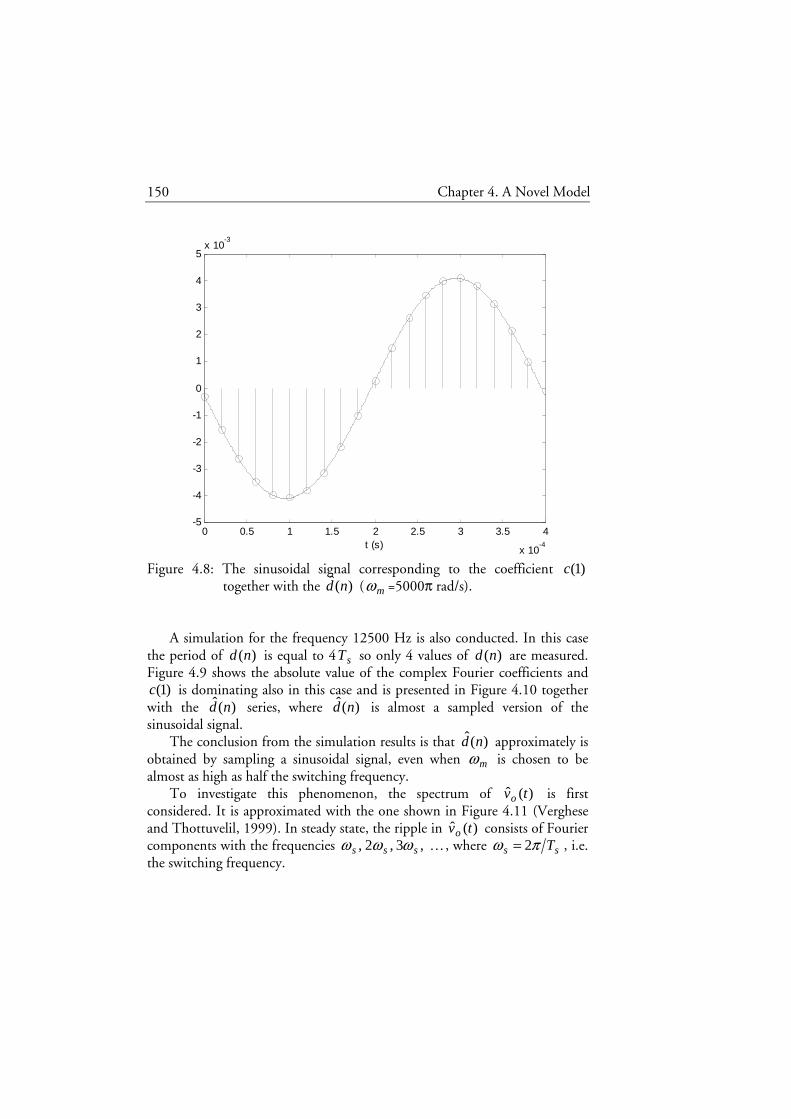
150 Chapter 4. A Novel Model
Figure 4.8: The sinusoidal signal corresponding to the coefficient )1(c together with the )(ˆ nd ( mω =5000π rad/s).
A simulation for the frequency 12500 Hz is also conducted. In this case
the period of )(nd is equal to 4 sT so only 4 values of )(nd are measured. Figure 4.9 shows the absolute value of the complex Fourier coefficients and
)1(c is dominating also in this case and is presented in Figure 4.10 together with the )(ˆ nd series, where )(ˆ nd is almost a sampled version of the sinusoidal signal.
The conclusion from the simulation results is that )(ˆ nd approximately is obtained by sampling a sinusoidal signal, even when mω is chosen to be almost as high as half the switching frequency.
To investigate this phenomenon, the spectrum of )(ˆ tvo is first considered. It is approximated with the one shown in Figure 4.11 (Verghese and Thottuvelil, 1999). In steady state, the ripple in )(ˆ tvo consists of Fourier components with the frequencies K,3,2, sss ωωω , where ss Tπω 2= , i.e. the switching frequency.
0 0.5 1 1.5 2 2.5 3 3.5 4
x 10-4
-5
-4
-3
-2
-1
0
1
2
3
4
5x 10
-3
t (s)
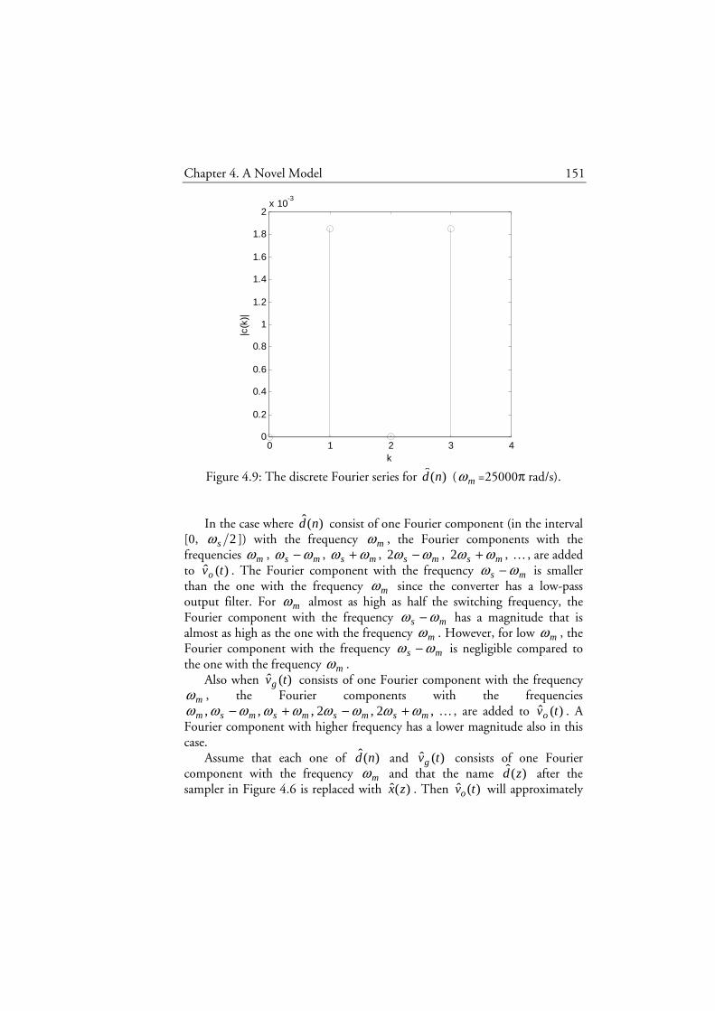
Chapter 4. A Novel Model 151
Figure 4.9: The discrete Fourier series for )(ˆ nd ( mω =25000π rad/s). In the case where )(ˆ nd consist of one Fourier component (in the interval
[0, 2sω ]) with the frequency mω , the Fourier components with the frequencies mω , ms ωω − , ms ωω + , ms ωω −2 , ms ωω +2 , K , are added to )(ˆ tvo . The Fourier component with the frequency ms ωω − is smaller than the one with the frequency mω since the converter has a low-pass output filter. For mω almost as high as half the switching frequency, the Fourier component with the frequency ms ωω − has a magnitude that is almost as high as the one with the frequency mω . However, for low mω , the Fourier component with the frequency ms ωω − is negligible compared to the one with the frequency mω .
Also when )(ˆ tvg consists of one Fourier component with the frequency
mω , the Fourier components with the frequencies K,2,2,,, msmsmsmsm ωωωωωωωωω +−+− , are added to )(ˆ tvo . A
Fourier component with higher frequency has a lower magnitude also in this case.
Assume that each one of )(ˆ nd and )(ˆ tvg consists of one Fourier component with the frequency mω and that the name )(ˆ zd after the sampler in Figure 4.6 is replaced with )(ˆ zx . Then )(ˆ tvo will approximately
0 1 2 3 40
0.2
0.4
0.6
0.8
1
1.2
1.4
1.6
1.8
2x 10
-3
k
|c(k
)|
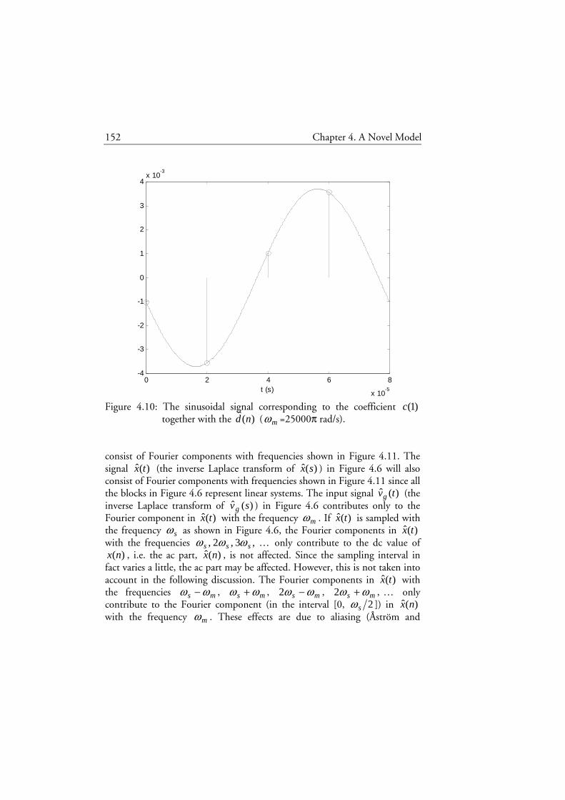
152 Chapter 4. A Novel Model
Figure 4.10: The sinusoidal signal corresponding to the coefficient )1(c together with the )(ˆ nd ( mω =25000π rad/s).
consist of Fourier components with frequencies shown in Figure 4.11. The signal )(ˆ tx (the inverse Laplace transform of )(ˆ sx ) in Figure 4.6 will also consist of Fourier components with frequencies shown in Figure 4.11 since all the blocks in Figure 4.6 represent linear systems. The input signal )(ˆ tvg (the inverse Laplace transform of )(ˆ svg ) in Figure 4.6 contributes only to the Fourier component in )(ˆ tx with the frequency mω . If )(ˆ tx is sampled with the frequency sω as shown in Figure 4.6, the Fourier components in )(ˆ tx with the frequencies K,3,2, sss ωωω only contribute to the dc value of
)(nx , i.e. the ac part, )(ˆ nx , is not affected. Since the sampling interval in fact varies a little, the ac part may be affected. However, this is not taken into account in the following discussion. The Fourier components in )(ˆ tx with the frequencies ms ωω − , ms ωω + , ms ωω −2 , ms ωω +2 , K only contribute to the Fourier component (in the interval [0, 2sω ]) in )(ˆ nx with the frequency mω . These effects are due to aliasing (Åström and
0 2 4 6 8
x 10-5
-4
-3
-2
-1
0
1
2
3
4x 10
-3
t (s)

Chapter 4. A Novel Model 153
Figure 4.11: The approximate spectrum of )(ˆ tvo .
Wittenmark, 1997, Section 7.4). Thus )(ˆ nx will only consist of one Fourier component (in the interval [0, 2sω ]) which explains the conclusion made from the simulation results.
Assume that the input signal )(ˆ tvo in Figure 4.6 is replaced with a signal consisting of just the Fourier component in )(ˆ tvo with the frequency mω . This introduce an error in )(ˆ tx . For low mω the relative error in )(ˆ tx is small since the Fourier components in )(ˆ tvo with the frequencies ms ωω − ,
ms ωω + , ms ωω −2 , ms ωω +2 , K are negligible compared to the one with the frequency mω . For mω almost as high as half the switching frequency, the Fourier component in )(ˆ tvo with the frequency ms ωω − is significant compared to the one with the frequency mω . This would introduce a large relative error in )(ˆ tx if the input signal )(ˆ tvg in Figure 4.6 is zero. In Section 3.5, it was concluded that the magnitude of )(ˆ tvo is much smaller than the magnitude of )(ˆ tvg at high frequencies (i.e. almost as high as nω ). The relative error in )(ˆ tx is therefore small also at high frequencies.
The important conclusions are now summarized for the case where )(ˆ tvg is a sinusoidal with the frequency mω :
• The discrete-time signal )(nd consists of just one Fourier
component (approximately) and it has the frequency mω . Therefore, )(nd can be obtained by sampling a sinusoidal signal.
• A good approximation of the signal )(ˆ tx in Figure 4.6 is obtained if the input signal )(ˆ tvo is replaced with a signal consisting of just the Fourier component in )(ˆ tvo with the frequency mω .
ω 2ωs-ωm ωs-ωm 0 2ωs+ωm ωs ωm 2ωs ωs+ωm

154 Chapter 4. A Novel Model
Figure 4.12: A model of the audio susceptibility.
A Novel Model of the Audio Susceptibility
To find a linear model of the audio susceptibility that is accurate from dc to half the switching frequency it is sufficient to consider just the case where the perturbation in the input voltage, )(ˆ tvg , is a sinusoidal signal with the frequency mω . The model should be accurate for any mω in the frequency interval. From the summarized conclusions above, it seems reasonable that an accurate model of the audio susceptibility can be obtained from the block diagram in Figure 4.12, where the block diagram in Figure 4.6 is combined with equation (4.5). )(ˆ sx is used as )(ˆ sd and the output )(ˆ svo from (4.5) is fed back to the input )(ˆ svo in the block diagram in Figure 4.6. The Fourier component in the output voltage with the frequency mω (see Section 2.11) is correctly predicted in (4.5) and it is enough to use this component as the
)(ˆ svo -input in the block diagram in Figure 4.6. In Section 4.4, it will be shown that the prediction of the audio susceptibility by means of the block diagram in Figure 4.12 has a serious shortcoming. At low frequencies, the prediction is very sensitive to modeling errors in the different blocks in the diagram.
4.3 Audio Susceptibility of the Buck Converter
In this section, the novel model derived in Section 4.2 is applied to the buck converter. The obtained expression is compared with simulation results, experimental result, and the Ridley and Tan models.
vo(s) ^
x(s) ^
m2(s) ^
m1(s) ^
vo(s) ^
vg(s) ^
von(s) ^
voff(s) ^ L 1
L 1
d(s) ^
vg(s) ^
vo(s) ^
ol
d(s) ^
vo(s) ^
(4.21) 4.1
Table

Chapter 4. A Novel Model 155
A Novel Expression
The audio susceptibility of the buck converter with current-mode control is obtained by using Figure 4.12, Table 4.1, (4.21), (2.92), (2.90), and (3.51):
( )
( )
( )( ),
1''
)(ˆ)(ˆ1)(ˆ
)(
1
)(ˆ)(
1)(ˆ
1
+−−
−−+−+
++
=
−−−
−−−
ss
sss
sTsTc
og
og
s
sDTo
s
sTsDT
ol
cg
gol
co
eeDmDL
VV
L
svsv
sT
e
L
sv
sT
ee
sden
CsRRV
svsden
CsRRDsv
(4.22)
where
( ) ( )
( ) ( )( ) .11
)( 2
CRRssLCsRR
LCRRsCRRLsRsden
cc
ccol
++++=++++=
(4.23)
(4.22) is rewritten by using (2.66), (2.68), and (2.39):
( )( )( )( ) ( )
( ) .)(ˆ)(ˆ1)(ˆ
1
)(ˆ11'
)(ˆ1')(
−−+−+
+++−
=+−
−−−
−−
−−
L
svsv
sT
e
L
sv
sT
eeCsRRV
svCsRRDeeDmL
V
sveeDmL
Vsden
og
s
sDTo
s
sTsDT
cg
gcsTsT
cg
osTsT
cg
ol
sss
ss
ss
(4.24)
(4.24) is rewritten:
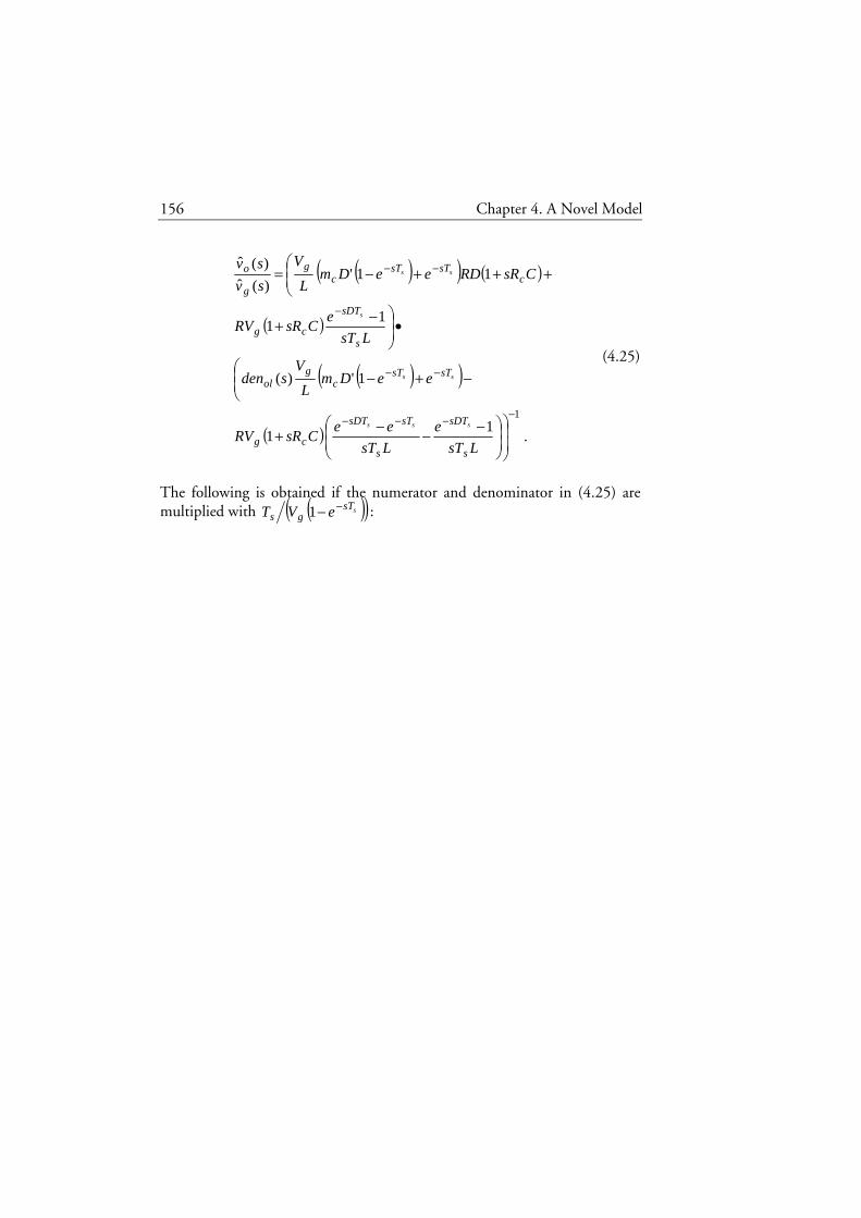
156 Chapter 4. A Novel Model
( )( ) ( )
( )
( )( )
( ) .1
1
1')(
11
11')(ˆ
)(ˆ
1−−−−
−−
−
−−
−−−+
−+−
•
−+
+++−=
LsT
e
LsT
eeCsRRV
eeDmL
Vsden
LsT
eCsRRV
CsRRDeeDmL
V
sv
sv
s
sDT
s
sTsDT
cg
sTsTc
gol
s
sDT
cg
csTsT
cg
g
o
sss
ss
s
ss
(4.25)
The following is obtained if the numerator and denominator in (4.25) are multiplied with ( )( )ssT
gs eVT −−1 :
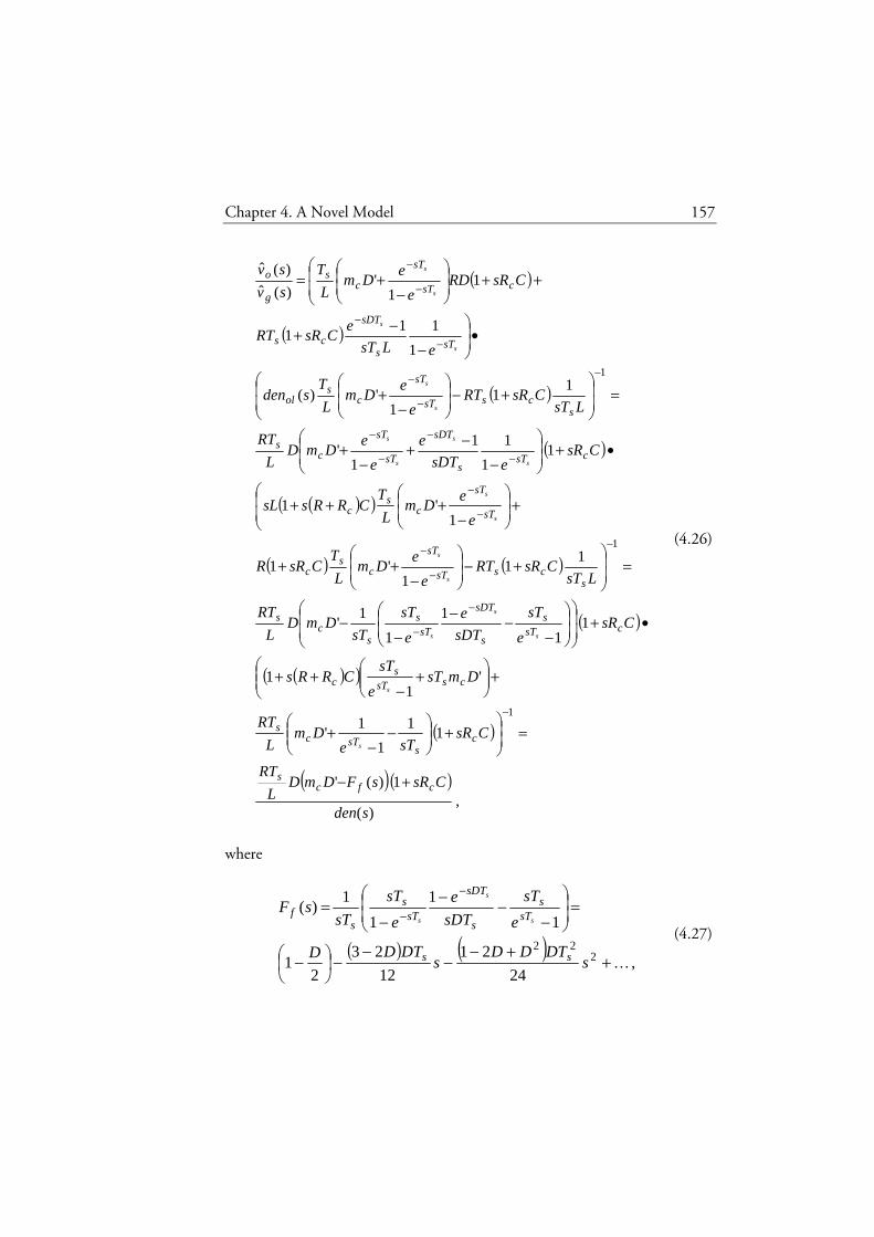
Chapter 4. A Novel Model 157
( )
( )
( )
( )
( )( )
( ) ( )
( )
( )( )
( )
( )( ),
)(
1)('
11
1
1'
'1
1
11
1
1
1'
11
1'1
1'1
11
11
1'
11
1')(
1
111
11
')(ˆ
)(ˆ
1
1
1
sden
CsRsFDmDL
RT
CsRsTe
DmL
RT
DmsTe
sTCRRs
CsRe
sT
sDT
e
e
sT
sTDmD
L
RT
LsTCsRRT
e
eDm
L
TCsRR
e
eDm
L
TCRRssL
CsResDT
e
e
eDmD
L
RT
LsTCsRRT
e
eDm
L
Tsden
eLsT
eCsRRT
CsRRDe
eDm
L
T
sv
sv
cfcs
cs
sTcs
cssTs
c
csTs
s
sDT
sTs
sc
s
scssT
sT
cs
c
sT
sT
cs
c
csTs
sDT
sT
sT
cs
scssT
sT
cs
ol
sTs
sDT
cs
csT
sT
cs
g
o
s
s
s
s
s
s
s
s
s
s
s
s
s
s
s
s
s
s
s
+−
=
+
−
−+
+
+−
++
•+
−−−
−−
=
+−
−++
+
−+++
•+
−−+
−+
=
+−
−+
•
−−+
++
−+=
−
−
−
−
−
−
−
−
−
−
−
−
−
−
−
−
−
−
−
(4.26)
where
( ) ( )
,24
21
12
23
21
1
1
1
1)(
222
K++−
−−
−
−
=
−−−
−=
−
−
sDTDD
sDTDD
e
sT
sDT
e
e
sT
sTsF
ss
sTs
s
sDT
sTs
sf
s
s
s
(4.27)

158 Chapter 4. A Novel Model
( )( )( )
( ) ,1)(1
'
')(1)(
CsRsT
sHDm
L
RT
DmsTsHCRRssden
cs
ec
s
csec
+
−−
++++=
(4.28)
and )(sHe is the same as in (3.10). The Taylor series of )(sF f is also shown in (4.27). (4.26) is the novel expression for the audio susceptibility of the buck converter with current-mode control. The denominator in this novel expression will now be compared with the denominators in the Ridley and Tan models.
If )(sHe in (4.28) is approximated by (3.14) and (3.54) is used, the following approximate denominator is obtained:
( )( )
( )
( )( ) ( )
( )( ) ( ) .12
15.0')(1
12
')(1
1
11
'
)(1)(
1
2
1
2
2
1
CsRsDmL
RTsFCRRs
CsRsT
TssT
DmL
RTsFCRRs
CsRsT
s
Q
s
DmL
RT
sFCRRssden
cn
cs
hc
cs
n
ss
cs
hc
cs
nznc
s
hc
+
−−+++
=+
−
−+++
=+
−−−
−
+++=
−
−
−
πω
πω
ωω
(4.29)
(4.29) is exactly the same as (3.72), i.e. the denominator in the Tan model. In Section 3.4, it was concluded that the denominator in the Tan model is almost the same as the denominator in the Ridley model, (3.62). The novel expression and the audio susceptibility predicted by the Ridley and Tan models thus have approximately the same denominator but three different numerators, compare (4.26), (3.61), and (3.71).
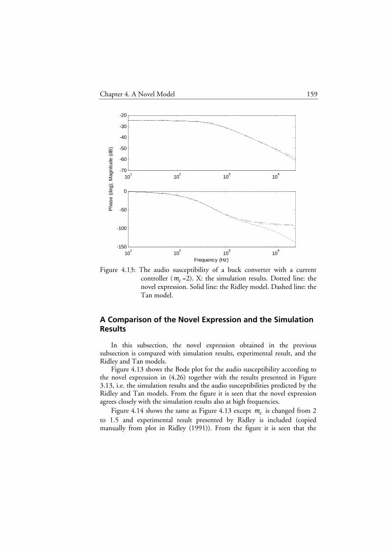
Chapter 4. A Novel Model 159
Figure 4.13: The audio susceptibility of a buck converter with a current controller ( cm =2). X: the simulation results. Dotted line: the novel expression. Solid line: the Ridley model. Dashed line: the Tan model.
A Comparison of the Novel Expression and the Simulation Results
In this subsection, the novel expression obtained in the previous subsection is compared with simulation results, experimental result, and the Ridley and Tan models.
Figure 4.13 shows the Bode plot for the audio susceptibility according to the novel expression in (4.26) together with the results presented in Figure 3.13, i.e. the simulation results and the audio susceptibilities predicted by the Ridley and Tan models. From the figure it is seen that the novel expression agrees closely with the simulation results also at high frequencies.
Figure 4.14 shows the same as Figure 4.13 except cm is changed from 2 to 1.5 and experimental result presented by Ridley is included (copied manually from plot in Ridley (1991)). From the figure it is seen that the
101
102
103
104
-70
-60
-50
-40
-30
-20
101
102
103
104
-150
-100
-50
0
Frequency (Hz)
Pha
se (
deg)
; M
agni
tude
(dB
)
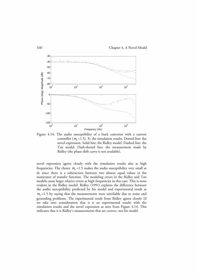
160 Chapter 4. A Novel Model
Figure 4.14: The audio susceptibility of a buck converter with a current controller ( cm =1.5). X: the simulation results. Dotted line: the novel expression. Solid line: the Ridley model. Dashed line: the Tan model. Dash-dotted line: the measurement made by Ridley (the phase shift curve is not available).
novel expression agrees closely with the simulation results also at high frequencies. The choice cm =1.5 makes the audio susceptibility very small at dc since there is a subtraction between two almost equal values in the numerator of transfer function. The modeling errors in the Ridley and Tan models cause larger relative errors at high frequencies in this case. This is most evident in the Ridley model. Ridley (1991) explains the difference between the audio susceptibility predicted by his model and experimental result at
cm =1.5 by saying that the measurements were unreliable due to noise and grounding problems. The experimental result from Ridley agrees closely (if we take into consideration that it is an experimental result) with the simulation results and the novel expression as seen from Figure 4.14. This indicates that it is Ridley’s measurements that are correct, not his model.
101
102
103
104
-80
-70
-60
-50
-40
-30
101
102
103
104
-150
-100
-50
0
Frequency (Hz)
Pha
se (
deg)
; M
agni
tude
(dB
)
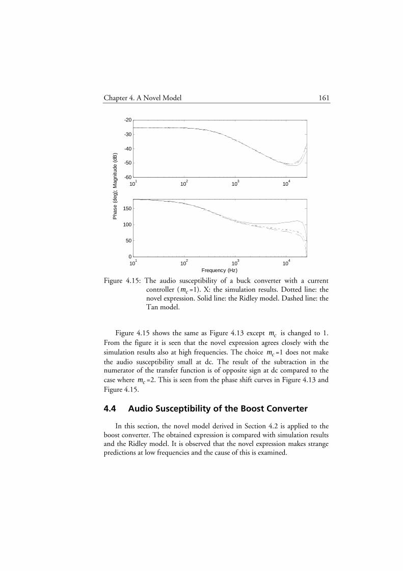
Chapter 4. A Novel Model 161
Figure 4.15: The audio susceptibility of a buck converter with a current controller ( cm =1). X: the simulation results. Dotted line: the novel expression. Solid line: the Ridley model. Dashed line: the Tan model.
Figure 4.15 shows the same as Figure 4.13 except cm is changed to 1.
From the figure it is seen that the novel expression agrees closely with the simulation results also at high frequencies. The choice cm =1 does not make the audio susceptibility small at dc. The result of the subtraction in the numerator of the transfer function is of opposite sign at dc compared to the case where cm =2. This is seen from the phase shift curves in Figure 4.13 and Figure 4.15.
4.4 Audio Susceptibility of the Boost Converter
In this section, the novel model derived in Section 4.2 is applied to the boost converter. The obtained expression is compared with simulation results and the Ridley model. It is observed that the novel expression makes strange predictions at low frequencies and the cause of this is examined.
101
102
103
104
-60
-50
-40
-30
-20
101
102
103
104
0
50
100
150
Frequency (Hz)
Pha
se (
deg)
; M
agni
tude
(dB
)
162 Chapter 4. A Novel Model
A Novel Expression
The audio susceptibility of the boost converter with current-mode control is obtained by using Figure 4.12, Table 4.1, (4.21), (2.144), (2.142), and (3.86):
( )
( ) ( )( )( )
( )( ),
1''
)(ˆ1)(ˆ)(ˆ
)(
1'''
)(ˆ)(
1')(ˆ
1
22
+−
−+−−
•++−
+
++
=
−−−
−−−
ss
sss
sTsTc
g
g
s
sDTgo
s
sTsDT
ol
ccc
g
gol
co
eeDmDL
V
L
sv
sT
e
L
svsv
sT
ee
sden
CsRLRRsDRDRRD
V
svsden
CsRRDsv
(4.30)
where
( ) ( ) ( ) ( )( ) ( )( ) ( )( ) ,1''
'''
)(2
CRRssLCsRRRRRDRD
LCRRsCDRRLsRRRRDRD
sden
cccc
cccc
ol
++++++=++++++
=
(4.31)
(4.30) is rewritten:
( )( )( )( ) ( )
( ) ( )( )( )
.)(ˆ1)(ˆ)(ˆ
1'''
)(ˆ1'1''
)(ˆ1''
)(
22
−+−−
•++−+
+++−
=+−
−−−
−−
−−
L
sv
sT
e
L
svsv
sT
ee
CsRLRRsDRDRRD
V
svCsRRDeeDmLD
V
sveeDmLD
Vsden
g
s
sDTgo
s
sTsDT
ccc
g
gcsTsT
cg
osTsT
cg
ol
sss
ss
ss
(4.32)
(4.32) is rewritten:

Chapter 4. A Novel Model 163
( )( ) ( )
( ) ( )( )( )
( )( )
( ) ( )( )( ) .1'''
1''
)(
1
1'''
1'1'')(ˆ
)(ˆ
1
22
22
−−−
−−
−−−
−−
−++−+
−+−
•
−−−
•++−+
+++−=
LsT
eeCsRLRRsDR
DRRD
V
eeDmLD
Vsden
LsT
ee
LsT
e
CsRLRRsDRDRRD
V
CsRRDeeDmLD
V
sv
sv
s
sTsDT
ccc
g
sTsTc
gol
s
sTsDT
s
sDT
ccc
g
csTsT
cg
g
o
ss
ss
sss
ss
(4.33)
The following is obtained if the numerator and denominator in (4.33) are multiplied with ( )( )ssT
gs eVTD −−1' :
( )
( )( ) ( )
( )( )( )1
22
22
1
11'
'
1')(
11'
'
1'1
')(ˆ
)(ˆ
−
−
−−
−
−
−
−
−−++−
+
−
−+
•
++−
+
−+
−+=
s
ss
s
s
s
s
sTs
sTsDT
ccc
s
sT
sT
cs
ol
scc
c
s
csT
sT
cs
g
o
eLsT
eeCsRLRRsDR
RRD
T
e
eDm
L
Tsden
LsTCsRLRRsDR
RRD
T
CsRRDe
eDm
L
T
sv
sv
(4.34)
The numerator in (4.34) is rewritten:
164 Chapter 4. A Novel Model
( )
( )( )( )
( )( ) ( )
( )
( ) ,1'
1
'
'1)(''
1'
1
'
'
1
1''
11
''
'
1''
11'
'
1'1
'
22
22
CsRRRD
RR
sTRRD
RDsFDmD
L
RT
CsRRRD
RR
sTRRD
RD
eDmD
L
RT
CsRsTRRDRD
LRRsDR
e
eDmD
L
RT
LsTCsRLRRsDR
RRD
T
CsRRDe
eDm
L
T
cc
c
scfc
s
cc
c
scsTc
s
csc
csT
sT
cs
scc
c
s
csT
sT
cs
s
s
s
s
s
+
++
+
+
−+−
=+
++
+
+
−−
+
=+
++−
−−
+
=++−+
−+
−+
−
−
−
−
(4.35)
where
.720122
1
1
11)( 3
3
K++−=−
−= sT
sT
esTsF ss
sTs
fs
(4.36)
The Taylor series of )(sF f is also shown in (4.36). The denominator in (4.34) is now rewritten:

Chapter 4. A Novel Model 165
( )( )( )
( )( )( )
( )( )
( ) ( )( )( )
( )( )
( )
( )
( )( )
( )
( )( ) ( )
( ) ,1
1
'
1'
'
'''
)('
11
'
''
'
'
)('
1')(
1'
11
'
'
1'
1'
'
'
1
1
'
1'
'
'
11
1
'
1
1''')(
1
1
'
11'
'
'
1
11
''
')(
1
111'
'
1
1)(')(
1
11'
'
1')(
'22
'22
'
'22
'22
'22
22
22
−
−+
−++
+−
+
++
−+
−
++++
=
−−++
+
−−
−+
+
−−
+
−−
+++−
+−+
++
=−
−++−+
−−
+++
+
++
+
=−
−++−+
−−
+
=−
−++−+
−
−+
−
−
−−
−
−
s
s
s
s
s
s
s
s
s
ss
s
s
s
s
s
ss
s
s
ss
s
s
sTs
TsD
c
s
c
cs
es
TsD
cc
cc
c
ecccs
ol
sTs
s
TsD
ccc
sTs
s
TsD
cc
sTs
TsD
c
s
sTs
csTs
c
sTc
csc
sol
sTs
TsD
ccc
s
sTs
ccc
c
cs
ol
sTs
sDTsT
ccc
s
sTs
olcs
ol
sTs
sTsDT
ccc
s
sT
sT
cs
ol
eTsD
eDR
RRDL
DT
RR
RRD
L
RDT
sHTsD
eCsR
RRD
RRDCRDR
RRDL
D
sHCRRsCRL
RDDm
L
Tsden
e
sT
TsD
eCsRRR
RRD
D
e
sT
TsD
eCRDR
RRDL
D
eTsD
eDR
RRDL
DT
e
sTCRRs
e
sTCR
L
RD
eRR
RRD
L
RDTDm
L
Tsden
eTsD
eCsRLRRsDR
RRDL
DT
eL
TCRRssLCsR
RR
RRDRD
DmL
Tsden
eLsT
eeCsRLRRsDR
RRD
T
eL
TsdenDm
L
Tsden
eLsT
eeCsRLRRsDR
RRD
T
e
eDm
L
Tsden
(4.37)
166 Chapter 4. A Novel Model
where )(sHe is the same as in (3.10). The novel expression for the audio susceptibility of the boost converter with current-mode control is obtained by using (4.35) and (4.37) to rewrite (4.34):
( ),
)(
1'
1
'
'1)(''
)(ˆ
)(ˆ
sden
CsRRRD
RR
sTRRD
RDsFDmD
L
RT
sv
sv
cc
c
scfc
s
g
o
+
++
+
+
−+−
=
(4.38)
where
( )( )
( )( ) ( )
( )
,'
1)(
'
1
'
'
''
''
'1)(
)('
11
'
'
'
'
1'
''
)(
'3
'32
se
s
TsD
cc
cs
cce
es
TsD
cc
c
c
c
ccc
ccs
TsDsH
TsD
e
RRD
RD
DRRD
RRD
L
RDT
CRRsCRL
RDsH
sHTsD
eCsR
RRD
DRR
RRDL
CRDR
CRRssLCsRRR
RRDRDD
L
mT
sden
s
s
−+
−++
+
+++
+−
+
++
−+
−
+++
+
++
=
(4.39)
)(sF f is defined in (4.36) and )(sHe is defined in (3.10).
If (4.38) and (4.39) are compared with (3.94) and (3.95), i.e. the Ridley model, it is seen that there are some differences both in the numerator and in the denominator.
A Comparison of the Novel Expression and the Simulation Results
In this subsection, the novel expression obtained in the previous subsection is compared with simulation results and the Ridley model. It is
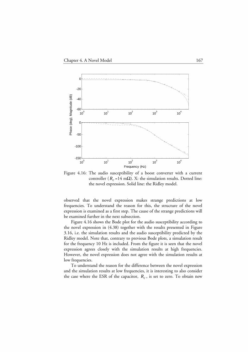
Chapter 4. A Novel Model 167
Figure 4.16: The audio susceptibility of a boost converter with a current controller ( cR =14 mΩ). X: the simulation results. Dotted line: the novel expression. Solid line: the Ridley model.
observed that the novel expression makes strange predictions at low frequencies. To understand the reason for this, the structure of the novel expression is examined as a first step. The cause of the strange predictions will be examined further in the next subsection.
Figure 4.16 shows the Bode plot for the audio susceptibility according to the novel expression in (4.38) together with the results presented in Figure 3.16, i.e. the simulation results and the audio susceptibility predicted by the Ridley model. Note that, contrary to previous Bode plots, a simulation result for the frequency 10 Hz is included. From the figure it is seen that the novel expression agrees closely with the simulation results at high frequencies. However, the novel expression does not agree with the simulation results at low frequencies.
To understand the reason for the difference between the novel expression and the simulation results at low frequencies, it is interesting to also consider the case where the ESR of the capacitor, cR , is set to zero. To obtain new
100
101
102
103
104
-60
-40
-20
0
100
101
102
103
104
-150
-100
-50
0
Frequency (Hz)
Pha
se (
deg)
; M
agni
tude
(dB
)
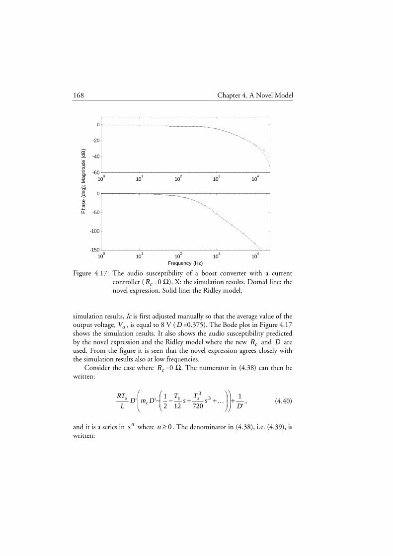
168 Chapter 4. A Novel Model
Figure 4.17: The audio susceptibility of a boost converter with a current controller ( cR =0 Ω). X: the simulation results. Dotted line: the novel expression. Solid line: the Ridley model.
simulation results, Ic is first adjusted manually so that the average value of the output voltage, oV , is equal to 8 V ( D =0.375). The Bode plot in Figure 4.17 shows the simulation results. It also shows the audio susceptibility predicted by the novel expression and the Ridley model where the new cR and D are used. From the figure it is seen that the novel expression agrees closely with the simulation results also at low frequencies.
Consider the case where cR =0 Ω. The numerator in (4.38) can then be written:
,'
1
720122
1'' 3
3
Ds
Ts
TDmD
L
RT ssc
s +
++−− K (4.40)
and it is a series in ns where 0≥n . The denominator in (4.38), i.e. (4.39), is written:
100
101
102
103
104
-60
-40
-20
0
100
101
102
103
104
-150
-100
-50
0
Frequency (Hz)
Pha
se (
deg)
; M
agni
tude
(dB
)
Chapter 4. A Novel Model 169
( )( )
( ) .'
1)(
'
11
'1)(
)('
11''
'3
'2
se
s
TsDs
e
es
TsDcs
TsDsH
TsD
e
L
RDTsRCsH
sHTsD
esRCsLRDD
L
mT
s
s
−−++
+−+++
(4.41)
The following expressions are written as Taylor series:
,6
'
2
'1
'
1 222'
K+++=−s
TDs
TD
TsD
e ss
s
TsD s
(4.42)
,122
11
)( 22
K++−=−
= sT
sT
e
sTsH ss
sTs
es
(4.43)
.24
'
6
'
2
1
'
1
'
11 2
22'
K+−−−=
−− sTD
sTD
TsDTsD
e ss
ss
TsD s
(4.44)
The denominator (4.39) is therefore also a series in ns where 0≥n . The gain of the denominator approaches a specific value as the frequency decreases. The same is true for the nominator.
Consider now the case where ≥cR 0 Ω. The term:
sc sTRRD
RD 1
'
'1
+
− (4.45)
makes the numerator in (4.38) to be a series in ns where 1−≥n . The term:
s
es
TsD
cc
cs
TsDsH
TsD
e
RRD
RD
DRRD
RRD
L
RDT s
'
1)(
'
1
'
'
''
'' '3
−+
−++
(4.46)
makes the denominator (4.39) also to be a series in ns where 1−≥n . Both the numerator and the denominator in (4.38) therefore contain an 1−s term. From Figure 4.16, it is seen that the gain starts to increase at approximately 100 Hz as the frequency decreases and this is due to the 1−s term in the numerator of (4.38). It is also seen that the gain stops increasing at
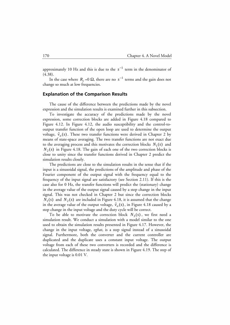
170 Chapter 4. A Novel Model
approximately 10 Hz and this is due to the 1−s term in the denominator of (4.38).
In the case where cR =0 Ω, there are no 1−s terms and the gain does not change so much at low frequencies.
Explanation of the Comparison Results
The cause of the difference between the predictions made by the novel expression and the simulation results is examined further in this subsection.
To investigate the accuracy of the predictions made by the novel expression, some correction blocks are added in Figure 4.18 compared to Figure 4.12. In Figure 4.12, the audio susceptibility and the control-to-output transfer function of the open loop are used to determine the output voltage, )(ˆ svo . These two transfer functions were derived in Chapter 2 by means of state-space averaging. The two transfer functions are not exact due to the averaging process and this motivates the correction blocks )(1 sN and
)(2 sN in Figure 4.18. The gain of each one of the two correction blocks is close to unity since the transfer functions derived in Chapter 2 predict the simulation results closely.
The predictions are close to the simulation results in the sense that if the input is a sinusoidal signal, the predictions of the amplitude and phase of the Fourier component of the output signal with the frequency equal to the frequency of the input signal are satisfactory (see Section 2.11). If this is the case also for 0 Hz, the transfer functions will predict the (stationary) change in the average value of the output signal caused by a step change in the input signal. This was not checked in Chapter 2 but since the correction blocks
)(1 sN and )(2 sN are included in Figure 4.18, it is assumed that the change in the average value of the output voltage, )(ˆ svo , in Figure 4.18 caused by a step change in the input voltage and the duty cycle will be correct.
To be able to motivate the correction block )(3 sN , we first need a simulation result. We conduct a simulation with a model similar to the one used to obtain the simulation results presented in Figure 4.17. However, the change in the input voltage, vghat, is a step signal instead of a sinusoidal signal. Furthermore, both the converter and the current controller are duplicated and the duplicate uses a constant input voltage. The output voltage from each of these two converters is recorded and the difference is calculated. The difference in steady state is shown in Figure 4.19. The step of the input voltage is 0.01 V.
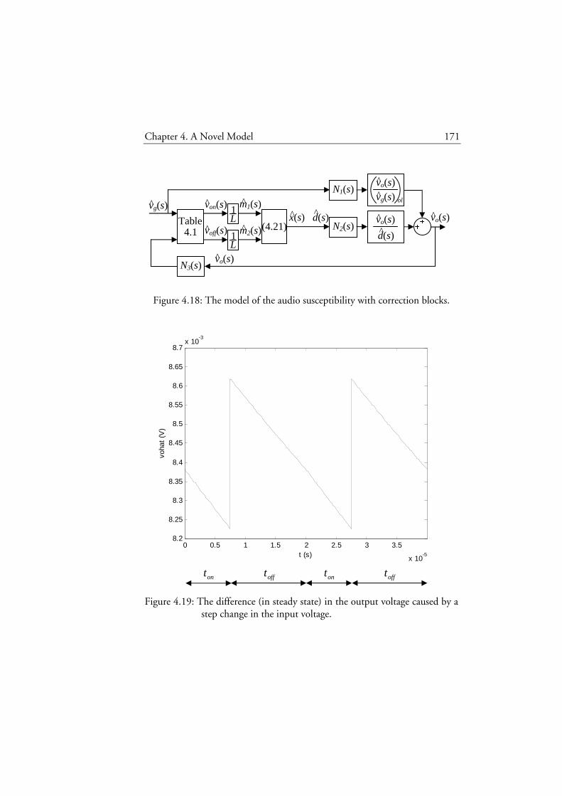
Chapter 4. A Novel Model 171
Figure 4.18: The model of the audio susceptibility with correction blocks.
ont offt ont offt
Figure 4.19: The difference (in steady state) in the output voltage caused by a
step change in the input voltage.
N3(s)
vo(s) ^
x(s) ^
m2(s) ^
m1(s) ^
vo(s) ^
vg(s) ^
von(s) ^
voff(s) ^ L 1
L 1
d(s) ^
vg(s) ^
vo(s) ^
ol
d(s) ^
vo(s) ^
(4.21) 4.1
Table
N1(s)
N2(s)
0 0.5 1 1.5 2 2.5 3 3.5
x 10-5
8.2
8.25
8.3
8.35
8.4
8.45
8.5
8.55
8.6
8.65
8.7x 10
-3
voha
t (V
)
t (s)

172 Chapter 4. A Novel Model
The correction block )(3 sN in Figure 4.18 can now be motivated as follows. The novel expression for the audio susceptibility should be able to predict the change in the average output voltage. The change in the voltage across the inductor during the time the transistor is off, )(ˆ tvoff , is equal to
)(ˆ)(ˆ tvtv go − according to Table 4.1. To obtain a good model, )(ˆ tvoff should not be calculated by using the average value of )(ˆ tvo . Instead, the average value of )(ˆ tvo as the transistor is off should be used. Note from Figure 4.19 that these two average values are not the same and )(3 sN must be used to correct this deviation.
If Figure 4.18 is used instead of Figure 4.12, the following equation corresponds to (4.30):
( )
( ) ( )( )( )
( )( ).
1''
)(ˆ1)(ˆ)(ˆ)(
)()(
1'''
)(ˆ)()(
1')(ˆ
1
3
2
22
1
+−
−+−−
•++−
+
++
=
−−−
−−−
ss
sss
sTsTc
g
g
s
sDTgo
s
sTsDT
ol
ccc
g
gol
co
eeDmDL
V
L
sv
sT
e
L
svsvsN
sT
ee
sNsden
CsRLRRsDRDRRD
V
svsNsden
CsRRDsv
(4.47)
By using (4.47) instead of (4.30), the corresponding equations to (4.32), (4.33), (4.34), (4.35), (4.37), (4.38), and (4.39) have been derived. Only the corresponding equations to (4.38), and (4.39) are presented here:
( ),
)(
1)(
'
1)(
'
')()()()('
')(ˆ
)(ˆ
2
2111
sden
CsRsN
RRD
RR
sTsN
RRD
RDsNsNsFsNDm
DL
RT
sv
sv
c
c
c
scfc
s
g
o
+
+
+
+
+
−+−
•
=
(4.48)
where

Chapter 4. A Novel Model 173
( )( )
( )( ) ( )
( )
.'
1)(
)()('
1
'
'
''
''
'1)(
)()()(
'
11
'
'
'
'
1'
''
)(
32
'3
32
'32
se
s
TsD
cc
cs
cce
e
s
TsD
cc
c
c
c
ccc
ccs
TsDsH
sNsNTsD
e
RRD
RD
DRRD
RRD
L
RDT
CRRsCRL
RDsH
sNsNsH
TsD
eCsR
RRD
RRD
RRDL
CRDR
CRRssLCsRRR
RRDRDD
L
mT
sden
s
s
•
−+
−++
+
+++
+
•−
+
++
−+
−
+++
+
++
=
(4.49)
If )(1 sN , )(2 sN and )(3 sN are equal to unity, (4.48) is the same as (4.38) and (4.49) is the same as (4.39).
Consider the case where cR =0 Ω. Then (4.48) and (4.49) can be simplified:
( )
)(
)('
11)()()()()(''
)(ˆ
)(ˆ
22111
sden
sNDsT
sNsNsNsFsNDmDL
RT
sv
sv
sfc
s
g
o
+
−+−
=
(4.50)
and

174 Chapter 4. A Novel Model
( )( )( )
.'
1)()()(
'
11
'
1)()()()('
1
1'')(
32
'3
32
'
2
se
s
TsDs
ees
TsD
cs
TsDsHsNsN
TsD
e
L
RDT
sRCsHsNsNsHTsD
e
sRCsLRDDL
mTsden
s
s
−−
+++−
+++=
(4.51)
The dc gain predicted by the model in Figure 4.18 is found by letting s tend to zero in (4.50) and (4.51). If )0(1N , )0(2N and )0(3N are equal to unity, the dc gain is calculated by using (4.36), (4.42), (4.43), and (4.44):
.
2
'2'
'
1
2
1''
)(ˆ
)(ˆ
0
lim3
3
L
RDTRD
L
mT
DDmD
L
RT
sv
sv
s scs
cs
g
o
−+
+
−=
→ (4.52)
The dc gain predicted by the Ridley model, (3.94), is exactly the same as (4.52). If )0(1N and )0(3N are equal to unity and )0(2N is not equal to unity, the numerator and the denominator must be multiplied with s before the dc gain is calculated:
( )
( ).
'
1
'
1)0(1
'
1)0(1'
)(ˆ
)(ˆ
0
lim
2
3
2
D
TDN
L
RDT
TND
L
RT
sv
sv
ss
s
s
s
g
o =−
−=
→(4.53)
If )0(2N and )0(3N are equal to unity and )0(1N is not equal to unity, the absolute value of the gain tend to infinity as s tend to zero. If )0(1N and
)0(2N are equal to unity and )0(3N is not equal to unity, the gain tend to zero as s tend to zero. This discussion shows that the predictions made by the model of the gain at low frequencies is very sensitive to errors in some parts of the model. From Figure 4.17, it was seen that the model in Figure 4.12 predicts the simulation results closely at low frequencies in the case where cR =0 Ω. The conclusion is that this is due to more good luck than good management.

Chapter 4. A Novel Model 175
From Figure 4.16, it was seen that the model in Figure 4.12 does not predict the simulation results closely at low frequencies in the case where
cR =14 mΩ. This may be due to absence of good luck. From Figure 4.16, it was also seen that the Ridley model predicts the simulation results closely at low frequencies in the case where cR =14 mΩ. This seems a little surprising since Ridley uses an approximate model of the PWM switch when the feedforward gains are derived. In Vorperian (1990), the PWM switch model depends on cR but Ridley uses this model as if cR =0 Ω.
4.5 Audio Susceptibility of the Buck-Boost Converter
In this section, the novel model derived in Section 4.2 is applied to the buck-boost converter. This is made in a way similar to the one used for the boost converter. The obtained expression is compared with simulation results and the Ridley model.
A Novel Expression
The audio susceptibility of the buck-boost converter with current-mode control is obtained by using Figure 4.12, Table 4.1, (4.21), (2.188), (2.186), and (3.104):
( )
( )( ) ( )( )
( )( ),
1''
)(ˆ1)(ˆ
)(
1'''
)(ˆ)(
1')(ˆ
1
2
+−
−+−
•+−
+
+
++
=
−−−
−−−
ss
sss
sTsTc
g
g
s
sDTo
s
sTsDT
ol
cc
cg
gol
co
eeDmDL
V
L
sv
sT
e
L
sv
sT
ee
sden
CsRsLDRDDRRD
RRV
svsden
CsRRDDsv
(4.54)
where

176 Chapter 4. A Novel Model
( ) ( ) ( ) ( )( ) ( )( ) ( )( ) ,1''
'''
)(2
CRRssLCsRRRRRDRD
LCRRsCDRRLsRRRRDRD
sden
cccc
cccc
ol
++++++=++++++
=
(4.55)
(4.54) is rewritten:
( )( )( )( ) ( )
( )( ) ( )( )
.)(ˆ1)(ˆ
1'''
)(ˆ1'1''
)(ˆ1''
)(
2
−+−
•+−+
+
+++−
=+−
−−−
−−
−−
L
sv
sT
e
L
sv
sT
ee
CsRsLDRDDRRD
RRV
svCsRRDDeeDmLD
V
sveeDmLD
Vsden
g
s
sDTo
s
sTsDT
cc
cg
gcsTsT
cg
osTsT
cg
ol
sss
ss
ss
(4.56)
(4.56) is rewritten:
( )( ) ( )
( )( ) ( )( )
( )( )( )
( ) ( )( ) .1'''
1''
)(
1
1'''
1'1'')(ˆ
)(ˆ
1
2
2
−−−
−−
−
−−
−+−+
+
−+−
•
−
•+−+
+
+++−=
LsT
eeCsRsLDRD
DRRD
RRV
eeDmLD
Vsden
LsT
e
CsRsLDRDDRRD
RRV
CsRRDDeeDmLD
V
sv
sv
s
sTsDT
cc
cg
sTsTc
gol
s
sDT
cc
cg
csTsT
cg
g
o
ss
ss
s
ss
(4.57)
The following is obtained if the numerator and denominator in (4.57) are multiplied with ( )( )ssT
gs eVTD −−1' :

Chapter 4. A Novel Model 177
( )
( ) ( )( )
( ) ( )( )1
2
2
1
11'
'
1')(
1
111'
'
1'1
')(ˆ
)(ˆ
−
−
−−
−
−
−
−
−
−
−−+−
++
−
−+
•
−−+−
++
++
−+=
s
ss
s
s
s
s
s
s
sTs
sTsDT
cc
cs
sT
sT
cs
ol
sTs
sDT
cc
cs
csT
sT
cs
g
o
eLsT
eeCsRsLDRD
RRD
RRT
e
eDm
L
Tsden
eLsT
eCsRsLDRD
RRD
RRT
CsRRDDe
eDm
L
T
sv
sv
(4.58)
The numerator in (4.58) is rewritten:
178 Chapter 4. A Novel Model
( )
( ) ( )( )
( )( )( )
( )( )( )
( )( )( )
( ) ( )
( )
( )( ) ( )
( )
( )
( )( ) ( )
( ) ( )
( ) ( ) ,1)(''
'
1)(
'
'1)(
'
'''
11
1
''
'
1
1
1
11
'
'
1
1
'
'1''
11
11
'''
1
11
'
'
1
1''
11
11
''
1
11
''
'
1''
1
1
11
''
'
1''
1
111'
'
1'1
'
2
1
2
2
2
CsRDsFD
D
RRD
RRD
sTsH
RRD
RRDsF
RRD
RRDDmD
L
RT
CsRDeD
e
D
D
RRD
RRD
eesDT
e
RRD
RRD
eRRD
RRDDmD
L
RT
CsRDesT
e
RRDRD
sLRRD
L
RT
esDT
e
RRD
RRD
eDmD
L
RT
CsRDesT
e
RRDRDD
sLDRR
esT
e
RRDRDD
RDRR
e
eDmD
L
RT
CsRD
esT
e
RRDRDD
sLDRDRR
e
eDmD
L
RT
eLsT
eCsRsLDRD
RRD
RRT
CsRRDDe
eDm
L
T
cfc
c
se
c
cf
c
cc
s
csT
sDT
c
c
sTsTs
sDT
c
c
sTc
cc
s
csTs
sDT
c
cs
sTs
sDT
c
csTc
s
csTs
sDT
c
c
sTs
sDT
c
csT
sT
cs
c
sTs
sDT
c
csT
sT
cs
sTs
sDT
cc
cs
csT
sT
cs
s
s
ss
s
s
s
s
s
s
s
s
s
s
s
s
s
s
s
s
s
s
s
s
s
+
++
+
++
−+++
−
=+
−−
++
+
−−
−−
++
−
−
++
−+
=+
−−
++
+
−−
++
−−
+
=+
−−
+−+
+
−−
++
+−
+
=+
•
−−
+−+
+−
+
=−
−+−++
++
−+
−
−
−
−
−
−
−
−
−
−
−
−
−
−
−
−
−
−
−
−
−
−
(4.59)
where

Chapter 4. A Novel Model 179
( ) ( )
,24
21
12
23
21
1
1
1
1)(
222
1
K++−
−−
−
−
=
−−−
−=
−
−
sDTDD
sDTDD
e
sT
sDT
e
e
sT
sTsF
ss
sTs
s
sDT
sTs
sf
s
s
s
(4.60)
( ).
12
231
2
'1
1
11)( 2
22
2 K++−
++=−
−= −
−s
TDDs
TD
e
e
DsF ss
sT
sDT
fs
s
(4.61)
and )(sHe is the same as in (3.10). The Taylor series of )(1 sF f and )(2 sF f are also shown in (4.60) and (4.61). Note that )(1 sF f in (4.60) is exactly the same as )(sF f in (4.27). The denominator in (4.58) is rewritten:

180 Chapter 4. A Novel Model
( ) ( )( )
( ) ( )( )
( )( )
( )( ) ( )( )
( )( )
( )( )
( )( )( ) ( )
( )
( )( )
( ) ( )
( )( ) ,
1
1
'
1'
'
'''
)('
11
'
''
'
'
)('
1')(
1'
11
'
'
1'
1'
'
'
1
1
'
1'
'
'
11
1
'
1
1''')(
1
1
'
11'
'
'
1
11
''
')(
1
111'
'
1
1)(')(
1
11'
'
1')(
'2
'2
'
'2
'2
'2
2
2
−
−++
−++
+−
+
++
−++
−
++++
=
−−+
++
−−
−++
+
−−
++
−−
+++−
+−+
++
=−
−+−++
−−
+++
+
++
+
=−
−+−++
−−
+
=−
−+−++
−
−+
−
−
−−
−
−
s
s
s
s
s
s
s
s
s
ss
s
s
s
s
s
ss
s
s
ss
s
s
sTs
TsD
c
cs
c
cs
es
TsD
cc
cc
c
c
ecccs
ol
sTs
s
TsD
cc
c
sTs
s
TsD
cc
c
sTs
TsD
c
cs
sTs
csTs
c
sTc
csc
sol
sTs
TsD
cc
cs
sTs
ccc
c
cs
ol
sTs
sDTsT
cc
cs
sTs
olcs
ol
sTs
sTsDT
cc
cs
sT
sT
cs
ol
eTsD
eRD
RRDL
RRDT
RR
RRD
L
RDT
sHTsD
eCsRD
RRD
RRDCRRD
RRDL
RRD
sHCRRsCRL
RDDm
L
Tsden
e
sT
TsD
eCsRD
RRD
RRD
e
sT
TsD
eCRRD
RRDL
RRD
eTsD
eRD
RRDL
RRDT
e
sTCRRs
e
sTCR
L
RD
eRR
RRD
L
RDTDm
L
Tsden
eTsD
eCsRsLDRD
RRDL
RRDT
eL
TCRRssLCsR
RR
RRDRD
DmL
Tsden
eLsT
eeCsRsLDRD
RRD
RRT
eL
TsdenDm
L
Tsden
eLsT
eeCsRsLDRD
RRD
RRT
e
eDm
L
Tsden
(4.62)
Chapter 4. A Novel Model 181
where )(sHe is the same as in (3.10). The novel expression for the audio susceptibility of the buck-boost converter with current-mode control is obtained by using (4.59) and (4.62) to rewrite (4.58):
( ) ( )
( ) ( ),
)(
1)(
''
'
1)(
'
'1)(
'
'''
)(ˆ
)(ˆ
2
1
sden
CsRDsF
D
D
RRD
RRD
sTsH
RRD
RRDsF
RRD
RRDDmD
L
RT
sv
sv
cf
c
c
se
c
cf
c
cc
s
g
o
+
++
+
++
−+++
−
=
(4.63)
where
( )( )
( )( )
( ) ( )
( )
( ),
'
1)(
'
1
'
'
''
''
'1)(
)('
11
'
'
'
'
1'
''
)(
'3
'3
se
s
TsD
c
c
c
cs
cce
es
TsD
cc
c
c
cc
ccc
cc
s
TsDsH
TsD
e
RRD
DRR
DRRD
RRD
L
RDT
CRRsCRL
RDsH
sHTsD
eCsR
RRD
DDRR
RRDL
CRRDRR
CRRssLCsRRR
RRDRDDm
L
T
sden
s
s
−+
+−
++
+
+++
+−
+
++
−+
+
−
+++
+
++
=
(4.64)
)(1 sF f is defined in (4.60), )(2 sF f is defined in (4.61), and )(sHe is
defined in (3.10). If (4.63) and (4.64) are compared with (3.112) and (3.113), i.e. the
Ridley model, it is seen that there are some differences both in the numerator and in the denominator.
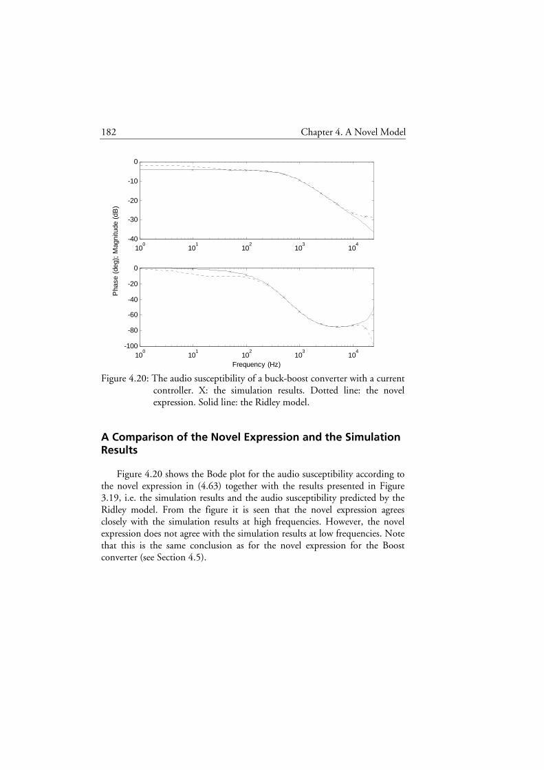
182 Chapter 4. A Novel Model
Figure 4.20: The audio susceptibility of a buck-boost converter with a current controller. X: the simulation results. Dotted line: the novel expression. Solid line: the Ridley model.
A Comparison of the Novel Expression and the Simulation Results
Figure 4.20 shows the Bode plot for the audio susceptibility according to the novel expression in (4.63) together with the results presented in Figure 3.19, i.e. the simulation results and the audio susceptibility predicted by the Ridley model. From the figure it is seen that the novel expression agrees closely with the simulation results at high frequencies. However, the novel expression does not agree with the simulation results at low frequencies. Note that this is the same conclusion as for the novel expression for the Boost converter (see Section 4.5).
100
101
102
103
104
-40
-30
-20
-10
0
100
101
102
103
104
-100
-80
-60
-40
-20
0
Frequency (Hz)
Pha
se (
deg)
; M
agni
tude
(dB
)
Chapter 4. A Novel Model 183
4.6 Summary and Concluding Remarks
A novel model for the audio susceptibility of converters with current-mode control was derived in this chapter. This was made by considering how the duty cycle depends on changes in the input and output voltages. The novel model was applied to the buck converter to obtain a novel expression for the audio susceptibility. The novel expression was compared with simulation results and the Ridley and Tan models. We concluded that the novel expression agrees closely with the simulation results also at high frequencies. The Ridley and Tan models do not agree closely with the simulation results at high frequencies due to modeling errors. The ramp that is used for slope compensation in current-mode control can be chosen such that the audio susceptibility is very small at dc for the buck converter. The predictions of the simulation results made by the Ridley and Tan models are worse for this case compared to other cases.
The novel model was also applied to the boost converter. The novel expression was compared with simulation results and the Ridley model. We concluded that the novel expression agrees closely with the simulation results at high frequencies, contrary to the Ridley model. However, the novel expression does not agree with the simulation results at low frequencies but the Ridley model does. In the case where the ESR of the capacitor, cR , is zero, the novel expression agrees closely with the simulation results also at low frequencies. An attempt to explain the predictions made by the novel expression for low frequencies was made. We saw that these predictions are very sensitive to errors in some parts of the derived model. The good result for cR =0 Ω is therefore due to more good luck than good management.
The novel model was also applied to the buck-boost converter. The novel expression was compared with simulation results and the Ridley model. We concluded that the novel expression agrees closely with the simulation results at high frequencies, contrary to the Ridley model. However, the novel expression does not agree with the simulation results at low frequencies but the Ridley model does. Thus, the novel expressions for the boost and buck-boost converters have similar properties.


185
Chapter 5 Improved Models
Models for converters with current-mode control were considered in Chapter 3. We showed that the way the changes in the input and output voltages are treated in the Ridley and Tan models introduces a modeling error at high frequencies. We also showed that this modeling error is significant for the audio susceptibility. A novel model for the audio susceptibility was derived in Chapter 4. In this chapter, this model is utilized to improve the Ridley and Tan models. In Chapter 6, the improved Ridley model will be approximated and then, in Chapter 7, used to analyze some properties that can be obtained when load current measurements are utilized for control.
5.1 Chapter Survey
The expressions for the audio susceptibility obtained by applying the Ridley and Tan models to the buck converter are improved in Section 5.2. The expressions for the audio susceptibility obtained by applying the Ridley model to the boost and buck-boost converters are improved in Section 5.3 and Section 5.4, respectively. A summary and concluding remarks are presented in Section 5.5.
5.2 Improved Expressions for the Buck Converter
The expression for the audio susceptibility obtained by applying the Ridley model to the buck converter is (see (3.58), (3.62), and (3.33))
( )
,)(
1'
)(ˆ
)(ˆ
sden
CsRkRDT
LDmD
L
RT
sv
svcf
isc
s
g
o
+
+
= (5.1)

186 Chapter 5. Improved Models
where
( )( ) ( )( ) ,15.0')(1)( 1 CsRDmL
RTsFCRRssden cc
shc +−+++= − (5.2)
,2
1
−−= D
L
RDTk is
f (5.3)
and )(sFh is defined in (3.19).
The expression for the audio susceptibility obtained by applying the Tan model to the buck converter is (see (3.68), (3.72), and (3.23))
( )
,)(
12
12
1'
)(ˆ
)(ˆ
sden
CsRskDT
LDmD
L
RT
sv
svc
nf
sc
s
g
o
+
−−+
=πω (5.4)
where
( )( ) ( ) ,12
15.0')(1
)(
1 CsRsDmL
RTsFCRRs
sden
cn
cs
hc +
−−+++
=
−
πω (5.5)
,2
'
L
TDDk s
f −= (5.6)
and )(sFh is defined in (3.19).
The novel expression for the audio susceptibility obtained by applying the novel model derived in Chapter 4 to the buck converter is (see (4.26) and (4.28))
( )( )
,)(
1)('
)(ˆ
)(ˆ
sden
CsRsFDmDL
RT
sv
sv cfcs
g
o+−
= (5.7)
where

Chapter 5. Improved Models 187
( )( )( )
( ) ,1)(1
'
')(1)(
CsRsT
sHDm
L
RT
DmsTsHCRRssden
cs
ec
s
csec
+
−−
++++=
(5.8)
)(sF f is defined in (4.27), and )(sHe is defined in (3.10).
In Section 4.3, it was concluded that the three expressions for the audio susceptibility presented above have approximately the same denominator but three different numerators. One way to improve the Ridley and Tan models is to modify the numerators in (5.1) and (5.4) in some way so that they are equal to the numerator in (5.7). The feedforward gain fk is not present in the denominators (5.2) and (5.5) and may therefore be used to modify the numerators in (5.1) and (5.4) without changing the denominators. Note that predictions of the control-to-output transfer function and the output impedance made by the Ridley and Tan models are not affected when fk is changed. This parameter is the gain of the feedforward of the input voltage, which is constant in the case where the control-to-output transfer function and the output impedance are considered. Note that modifying only fk may not be the most suitable solution. This will be discussed in Section 5.5.
The improvement of the Ridley model is first considered. The following equation is obtained if the numerator in (5.1) is put equal to the numerator in (5.7):
( )
( )( ) .1)('
1)('
CsRsFDmDL
RT
CsRskRDT
LDmD
L
RT
cfcs
cfis
cs
+−
=+
+
(5.9)
The new fk depends on s and this is prepared for in (5.9). The transfer function )(sk f is calculated by using (5.9):
.)()( sFL
RDTsk f
isf −= (5.10)
where )(sF f is defined in (4.27). Note that the 0s term in (5.10) is equal to (5.3).

188 Chapter 5. Improved Models
The improvement of the Tan model is now considered. The following equation is obtained if the numerator in (5.4) is put equal to the numerator in (5.7):
( )
( )( ) .1)('
12
12
1)('
CsRsFDmDL
RT
CsRsskDT
LDmD
L
RT
cfcs
cn
fs
cs
+−
=+
−−+
πω(5.11)
)(sk f is found by rearranging (5.11):
.2
12
1)()(
−−−=
nf
sf ssF
L
DTsk
πω (5.12)
where )(sF f is defined in (4.27). Note that the 0s term in (5.12) is equal to (5.6).
5.3 Improved Expression for the Boost Converter
The expression for the audio susceptibility obtained by applying the Ridley model to the boost converter is improved in this section. The methodology is slightly different compared to the one used for the buck converter since the novel expression exhibits poor low-frequency predictions. A combined expression is first derived and this expression is then used to derive a new feedforward gain )(sk f .
The expression for the audio susceptibility obtained by applying the Ridley model to the boost converter is (see (3.94) and (3.95))
( ),
)(1
1'
5.0'
'
)(ˆ
)(ˆ1
2
2
sdenCsR
s
RD
RR
R
RRDmD
L
RT
sv
sv
c
n
ccc
s
g
o−+
+
++
−+
=ω
(5.13)
where

Chapter 5. Improved Models 189
( )( )
( ) ( )
( ) ,'
'
'
'2)(
'11
2
'
1'
''
)(
22
3
+++
+
+
+−+
−
+++
+
+++
=
RD
RRDCRRs
RD
RRDsH
DR
LRRsCsR
L
TRD
CRRssLCsRRR
RRDRD
R
RRD
L
mT
sden
cc
ce
cc
s
ccc
cccs
(5.14)
and )(sHe is defined in (3.35). The novel expression for the audio susceptibility obtained by applying the
novel model derived in Chapter 4 to the boost converter is (see (4.38) and (4.39))
( ),
)(1
'
1
'
'1)(''
)(ˆ
)(ˆ1 sdenCsR
RRD
RR
sTRRD
RDsFDmD
L
RT
sv
sv
c
c
c
scfc
s
g
o−+
++
+
+
−+−
= (5.15)
where
( )( )
( )( ) ( )
( )
,'
1)(
'
1
'
'
''
''
'1)(
)('
11
'
'
'
'
1'
''
)(
'3
'32
se
s
TsD
cc
cs
cce
es
TsD
cc
c
c
c
ccc
ccs
TsDsH
TsD
e
RRD
RD
DRRD
RRD
L
RDT
CRRsCRL
RDsH
sHTsD
eCsR
RRD
DRR
RRDL
CRDR
CRRssLCsRRR
RRDRDD
L
mT
sden
s
s
−+
−++
+
+++
+−
+
++
−+
−
+++
+
++
=
(5.16)
)(sF f is defined in (4.36), and )(sHe is defined in (3.10).
In Section 4.4, it was concluded that the expression (5.13) agrees closely

190 Chapter 5. Improved Models
Figure 5.1: The denominator in the audio susceptibility of a boost converter with a current controller ( cR =14 mΩ). Dotted line: the novel expression. Solid line: the Ridley model.
with the simulation results at low frequencies but not at high frequencies. It was also concluded that the novel expression (5.15) agrees closely with the simulation results at high frequencies but not at low frequencies. These two expressions will now be combined to an expression that agrees closely with the simulation results both at low and high frequencies.
The Bode plots for the denominators in (5.13) and (5.15) are shown in Figure 5.1. The parameter values shown in Table 2.5 are used. The two denominators agree closely at high frequencies. The maximum difference is approximately 0.3 dB and 2 degrees in the frequency interval 500 - 25000 Hz. (5.15) is not good at low frequencies in the case where cR =14 mΩ. Figure 5.2 shows the same as Figure 5.1 except cR is changed from 14 mΩ to 0 Ω. In this case, the two denominators agree closely in the whole presented frequency interval. The maximum difference is approximately 0.1 dB and 2 degrees.
This discussion shows that it is reasonable to replace the denominator in
100
101
102
103
104
0
10
20
30
40
50
100
101
102
103
104
-100
-50
0
50
100
150
Frequency (Hz)
Pha
se (
deg)
; M
agni
tude
(dB
)
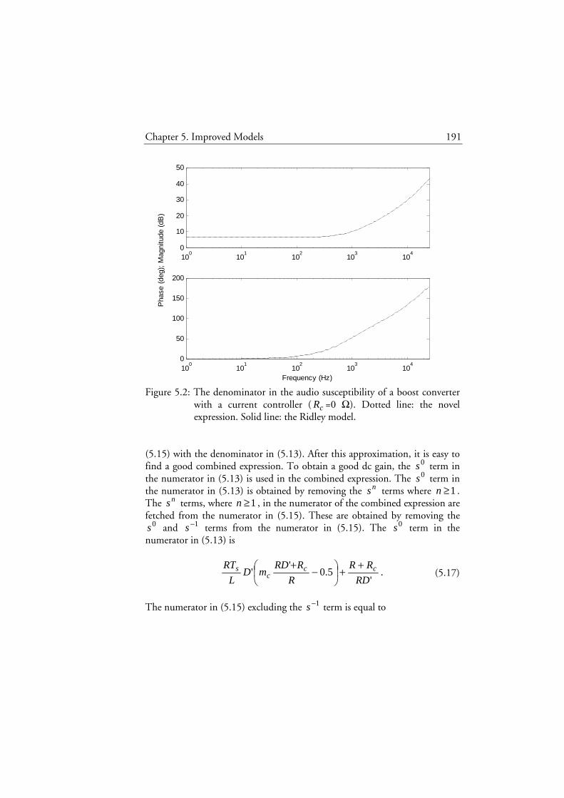
Chapter 5. Improved Models 191
Figure 5.2: The denominator in the audio susceptibility of a boost converter with a current controller ( cR =0 Ω). Dotted line: the novel expression. Solid line: the Ridley model.
(5.15) with the denominator in (5.13). After this approximation, it is easy to find a good combined expression. To obtain a good dc gain, the 0s term in the numerator in (5.13) is used in the combined expression. The 0s term in the numerator in (5.13) is obtained by removing the ns terms where 1≥n . The ns terms, where 1≥n , in the numerator of the combined expression are fetched from the numerator in (5.15). These are obtained by removing the
0s and 1−s terms from the numerator in (5.15). The 0s term in the numerator in (5.13) is
.'
5.0'
'RD
RR
R
RRDmD
L
RT ccc
s ++
−+
(5.17)
The numerator in (5.15) excluding the 1−s term is equal to
100
101
102
103
104
0
10
20
30
40
50
100
101
102
103
104
0
50
100
150
200
Frequency (Hz)
Pha
se (
deg)
; M
agni
tude
(dB
)
192 Chapter 5. Improved Models
( ) .'
)(''c
cfc
s
RRD
RRsFDmD
L
RT
++
+− (5.18)
By using (4.36), the following is obtained if the 0s term is removed from (5.18):
.2
1)('
−− sFD
L
RTf
s (5.19)
The numerator in the combined expression is now obtained by adding (5.17) and (5.19):
( )
.'
)('
'
5.0)(''
5.0'
'
RD
RRsF
R
RRDmD
L
RT
sFDL
RT
RD
RR
R
RRDmD
L
RT
cf
cc
s
fscc
cs
++
−+
=−−+
+
−+
(5.20)
By using (5.20), the combined expression for the audio susceptibility is obtained:
( ),
)(1
')(
''
)(ˆ
)(ˆ1 sdenCsR
RD
RRsF
R
RRDmD
L
RT
sv
sv
c
cf
cc
s
g
o−+
++
−
+
= (5.21)
where )(sden is defined in (5.14) and )(sF f is defined in (4.36).
Figure 5.3 shows the Bode plot for the audio susceptibility according to the combined expression in (5.21) together with the results presented in Figure 4.16, i.e. the simulation results and the audio susceptibilities predicted by the novel expression, (5.15), and the Ridley model, (5.13). From the figure it is seen that the combined expression agrees closely with the simulation results both at low and high frequencies.
(5.13) is the expression for the audio susceptibility obtained by applying the Ridley model to the boost converter. This expression is written as follows (see (3.91) and (3.84)):

Chapter 5. Improved Models 193
Figure 5.3: The audio susceptibility of a boost converter with a current controller. X: the simulation results. Dashed line: the combined expression. Dotted line: the novel expression. Solid line: the Ridley model. Note that the dashed line almost coincides with the solid line at low frequencies.
( ),
)(1
1
2
11
'
1'
''
)(ˆ
)(ˆ
1
2
2
sdenCsRk
RT
L
R
R
D
Ts
s
RD
RRk
RT
L
R
RRDmD
L
RT
sv
sv
cf
is
cs
n
cf
is
cc
s
g
o
−+
+
+
−
+
++
+
+=
ω (5.22)
where
,2L
RTk is
f −= (5.23)
and )(sden is defined in (5.14).
100
101
102
103
104
-60
-40
-20
0
100
101
102
103
104
-150
-100
-50
0
Frequency (Hz)
Pha
se (
deg)
; M
agni
tude
(dB
)

194 Chapter 5. Improved Models
The combined expression will now be used to improve the Ridley model. Note that the denominator in (5.21) and (5.22) are exactly the same. One way to improve the Ridley model is to modify the numerator in (5.22) in some way so that it is equal to the numerator in (5.21). The feedforward gain
fk is not present in the denominator in (5.22) and may therefore be used to modify the numerator in (5.22) without changing the denominator. The following equation is obtained if the numerator in (5.22) is put equal to the numerator in (5.21):
.'
)('
'
)(2
11
'
1'
)('
'2
2
RD
RRsF
R
RRDmD
L
RT
skRT
L
R
R
D
Ts
s
RD
RRsk
RT
L
R
RRDmD
L
RT
cf
cc
s
fis
cs
n
cf
is
cc
s
++
−+
=
+
+
−
+
++
+
+ω
(5.24)
The new fk depends on s and this is prepared for in (5.24). )(sk f is calculated by using (5.24):
( ) ,)('
)(2
11
'
')('
2
2
sFDL
RT
skRT
L
R
R
D
Ts
s
RD
RRsk
RT
LD
L
RT
fs
fis
cs
n
cf
is
s
−
=
+
+
−
++
ω
(5.25)
Chapter 5. Improved Models 195
( )
.
1'
1
12
1'
)(2
2
1'
1
1''
2)(2
2
1'
1
1'2'
)(
1'
''
2
11
'')('
')(
2
22
2
22
2
22
2
22
2
22
2
2
+−
+
−−
−
=
+−
+−+
+−
=
+−
+++
−−
=
+−
+++
−−
=
R
R
RD
Ls
R
Rs
TRD
LssF
L
RT
R
R
RD
Ls
R
R
RD
Ls
s
DR
RR
T
LsF
L
RT
R
R
RD
Ls
R
R
RD
RTs
s
DR
RRRsF
L
RT
RT
L
R
R
D
Ts
RT
LD
L
RT
RD
R
R
R
D
Ts
s
RD
RRsFD
L
RT
RD
R
sk
c
c
nsf
is
c
c
n
c
sf
is
c
cis
n
icf
is
is
cs
is
si
cs
n
cf
si
f
ω
ω
ω
ω
(5.26)
(5.26) is rewritten by using (3.13):
,
1'
1
12
1'
)(2
2)(
2
2
+−
+
−−
−=
R
R
RD
Ls
R
Rs
RD
LssF
L
RTsk
c
c
nf
isf
πω (5.27)
where )(sF f is defined in (4.36). Note that the 0s term in (5.27) is equal to (5.23). Note also that )(sk f is an unstable transfer function since its pole is in the right half plane.

196 Chapter 5. Improved Models
5.4 Improved Expression for the Buck-Boost Converter
The expression for the audio susceptibility obtained by applying the Ridley model to the buck-boost converter is improved in this section. The methodology is analogous to the one used for the boost converter.
The expression for the audio susceptibility obtained by applying the Ridley model to the buck-boost converter is (see (3.112) and (3.113))
( ),
)(1
21
'21
''
)(ˆ
)(ˆ11
2
2
sdenCsRD
DTs
s
D
DD
RR
RRDmD
L
RT
sv
sv
c
s
nc
cc
s
g
o−− +
+
++
−−
++
=ω
(5.28)
where
( )( )
( )
( )( ) .
'
'
'
1')(
'11
2
'
1'
''
)(
2
3
++
+++
+
−+
−
+++
+
++
++
=
D
RRDsC
DRR
RDRDsH
RD
LDsCsR
L
TRD
CRRssLCsRRR
RRDRD
RR
RRD
L
mT
sden
c
c
ce
cs
ccc
c
c
ccs
(5.29)
and )(sHe is defined in (3.35). The novel expression for the audio susceptibility obtained by applying the
novel model derived in Chapter 4 to the buck-boost converter is (see (4.63) and (4.64))
Chapter 5. Improved Models 197
( ) ( )
( )( )
,)(1
1)(
''
'
1)(
'
'1)(
'
'''
)(ˆ
)(ˆ
112
1
sdenCsRDsF
D
D
RRD
RRD
sTsH
RRD
RRDsF
RRD
RRDDmD
L
RT
sv
sv
cf
c
c
se
c
cf
c
cc
s
g
o
−− +
++
+
++
−+++
−
=
(5.30)
where
( )( )
( )( )
( ) ( )
( )
( ),
'
1)(
'
1
'
'
''
''
'1)(
)('
11
'
'
'
'
1'
''
)(
'3
'3
se
s
TsD
c
c
c
cs
cce
es
TsD
cc
c
c
cc
ccc
cc
s
TsDsH
TsD
e
RRD
DRR
DRRD
RRD
L
RDT
CRRsCRL
RDsH
sHTsD
eCsR
RRD
DDRR
RRDL
CRRDRR
CRRssLCsRRR
RRDRDDm
L
T
sden
s
s
−+
+−
++
+
+++
+−
+
++
−+
+
−
+++
+
++
=
(5.31)
)(1 sF f is defined in (4.60), )(2 sF f is defined in (4.61), and )(sHe is
defined in (3.10). In Section 4.5, it was concluded that the expression (5.28) agrees closely
with the simulation results at low frequencies but not at high frequencies. It was also concluded that the novel expression (5.30) agrees closely with the simulation results at high frequencies but not at low frequencies. These two expressions will now be combined to an expression that agrees closely with the simulation results both at low and high frequencies.
The Bode plots for the denominators in (5.28) and (5.30) are shown in Figure 5.4. The parameter values shown in Table 2.6 are used. The two denominators agree closely at high frequencies. The maximum difference is approximately 0.4 dB and 4 degrees in the frequency interval 250 - 25000 Hz. (5.30) is not good at low frequencies in the case where cR =14 mΩ. Figure 5.5 shows the same as Figure 5.4 except cR is changed from 14 mΩ

198 Chapter 5. Improved Models
Figure 5.4: The denominator in the audio susceptibility of a buck-boost converter with a current controller ( cR =14 mΩ). Dotted line: the novel expression. Solid line: the Ridley model.
to 0 Ω. In this case, the two denominators agree closely in the whole presented frequency interval. The maximum difference is approximately 0.3 dB and 3 degrees.
This discussion shows that it is reasonable to replace the denominator in (5.30) with the denominator in (5.28). After this approximation, it is easy to find a good combined expression. To obtain a dc gain that agrees closely with the simulation results, the 0s term in the numerator in (5.28) is used in the combined expression. The 0s term in the numerator in (5.28) is obtained by removing the ns terms where 1≥n . The ns terms, where 1≥n , in the numerator of the combined expression are fetched from the numerator in (5.30). These are obtained by removing the 0s and 1−s terms from the numerator in (5.30). The 0s term in the numerator in (5.28) is
.'2
1'
'D
DD
RR
RRDmD
L
RT
c
cc
s +
−−
++
(5.32)
100
101
102
103
104
0
10
20
30
40
100
101
102
103
104
-100
-50
0
50
100
150
Frequency (Hz)
Pha
se (
deg)
; M
agni
tude
(dB
)

Chapter 5. Improved Models 199
Figure 5.5: The denominator in the audio susceptibility of a buck-boost converter with a current controller ( cR =0 Ω). Dotted line: the novel expression. Solid line: the Ridley model.
By using (4.43), the numerator in (5.30) excluding the 1−s term is obtained:
( )
( ) ( )
( ).)(
''
'
11)(
'
'1
)('
'''
2
1
sFD
D
RRD
RRD
sTsH
RRD
RRD
sFRRD
RRDDmD
L
RT
fc
c
se
c
c
fc
cc
s
++
+
−
++
−
+
++
−
(5.33)
By using (4.43), (4.60), and (4.61), the following is obtained if the 0s term is removed from (5.33):
100
101
102
103
104
0
10
20
30
40
100
101
102
103
104
0
50
100
150
200
Frequency (Hz)
Pha
se (
deg)
; M
agni
tude
(dB
)
200 Chapter 5. Improved Models
( )
( )
( ) ( ).1)(''
'
1
21)(
'
'1
21)(
'
''
2
1
−++
+
−−
++
−
+
−−
++
−
sFD
D
RRD
RRD
sTs
TsH
RRD
RRD
DsF
RRD
RRDD
L
RT
fc
c
s
se
c
c
fc
cs
(5.34)
The numerator in the combined expression is now obtained by adding (5.32) and (5.34):
( )
( )
( ) ( ).1)(''
'
1
21)(
'
'1
21)(
'
''
'21
''
2
1
−++
+
−−
++
−
+
−−
++
−
++
−−
++
sFD
D
RRD
RRD
sTs
TsH
RRD
RRD
DsF
RRD
RRDD
L
RT
D
DD
RR
RRDmD
L
RT
fc
c
s
se
c
c
fc
cs
c
cc
s
(5.35)
One part of (5.35) can be rewritten as follows:
( )
( )( )
( )( )
( )( ) .
21
')(
'
'
211
'
')(
'
'
21
'
'
21)(
'
'
21)(
'
'
21
1
1
1
1
−
++
++
−
=
−
−
++
+++
−
=
−
++
+
−−
++
−
=
−−
++
−
−−
D
RRD
DRsF
RRD
RRD
D
RRD
RRDsF
RRD
RRD
D
RRD
RRDDsF
RRD
RRD
DsF
RRD
RRDD
c
cf
c
c
c
cf
c
c
c
cf
c
c
fc
c
(5.36)
Another part of (5.35) can be rewritten as follows:

Chapter 5. Improved Models 201
( ) ( )( )
( )( )
( ) .'
)(''
'
'
'1)(
''
'
1)(''
'
'
2
2
2
+
+++
=
++
+−++
=−++
+
c
cf
c
c
c
cf
c
c
fc
c
RRD
DRsF
D
D
RRD
RRD
RRD
RRDsF
D
D
RRD
RRD
sFD
D
RRD
RRD
D
D
(5.37)
By using (5.36) and (5.37) to rewrite (5.35), the combined expression for the audio susceptibility is obtained:
( )( )
( )
( )( ) ( )
,)(1
1
')(
''
'
1
21)(
'
'1
21
')(
'
'''
)(ˆ
)(ˆ
112
1
sdenCsRDRRD
DRsF
D
D
RRD
RRD
sTs
TsH
RRD
RRD
D
RRD
DRsF
RRD
RRD
RR
RRDmD
L
RT
sv
sv
cc
cf
c
c
s
se
c
c
c
cf
c
c
c
cc
s
g
o
−− +
+
+++
+
−−
++
−
+
−
++
++
−++
=
(5.38)
where )(sden is defined in (5.29), )(1 sF f is defined in (4.60), )(2 sF f is defined in (4.61), and )(sHe is defined in (3.10).
Figure 5.6 shows the Bode plot for the audio susceptibility according to the combined expression in (5.38) together with the results presented in Figure 4.20, i.e. the simulation results and the audio susceptibilities predicted by the novel expression, (5.30), and the Ridley model, (5.28). From the figure it is seen that the combined expression agrees closely with the simulation results both at low and high frequencies.
(5.28) is the expression for the audio susceptibility obtained by applying the Ridley model to the buck-boost converter. This expression is now written as follows (see (3.109) and (3.102)):

202 Chapter 5. Improved Models
Figure 5.6: The audio susceptibility of a buck-boost converter with a current controller. X: the simulation results. Dashed line: the combined expression. Dotted line: the novel expression. Solid line: the Ridley model. Note that the dashed line almost coincides with the solid line at low frequencies.
( ),
)(1
1
2'
1'
''
)(ˆ
)(ˆ
11
2
2
sdenCsRDk
RT
LD
D
Ts
s
D
Dk
RDT
L
RR
RRDmD
L
RT
sv
sv
cf
is
s
nf
isc
cc
s
g
o
−− +
+
−
++
+
++
=ω
(5.39)
where
,2
1
−−= D
L
RDTk is
f (5.40)
and )(sden is defined in (5.29).
100
101
102
103
104
-40
-30
-20
-10
0
100
101
102
103
104
-100
-80
-60
-40
-20
0
Frequency (Hz)
Pha
se (
deg)
; M
agni
tude
(dB
)
Chapter 5. Improved Models 203
The combined expression will now be used to improve the Ridley model. Note that the denominator in (5.38) and (5.39) are exactly the same. One way to improve the Ridley model is to modify the numerator in (5.39) in some way so that it is equal to the numerator in (5.38). The feedforward gain
fk is not present in the denominator in (5.39) and may therefore be used to modify the numerator in (5.39) without changing the denominator. The following equation is obtained if the numerator in (5.39) is put equal to the numerator in (5.38):
( )( )
( )
( )( ) .
')(
''
'
1
21)(
'
'1
21
')(
'
'''
)(2'
1'
)('
'
2
1
2
2
+
+++
+
−−
++
−
+
−
++
++
−++
=
+
−
++
+
++
c
cf
c
c
s
se
c
c
c
cf
c
c
c
cc
s
fis
s
nf
isc
cc
s
RRD
DRsF
D
D
RRD
RRD
sTs
TsH
RRD
RRD
D
RRD
DRsF
RRD
RRD
RR
RRDmD
L
RT
skRT
LD
D
Ts
s
D
Dsk
RDT
L
RR
RRDmD
L
RT
ω
(5.41)
The new fk depends on s and this is prepared for in (5.41). )(sk f is calculated by using (5.41):
( )( )
( )
( )( ) ,
')(
''
'
1
21)(
'
'1
21
')(
'
''
)(2'
1'
)('
2
1
2
2
+
+++
+
−−
++
−
−
−
++
++
−
=
+−
++
c
cf
c
c
s
se
c
c
c
cf
c
cs
fis
s
nf
is
s
RRD
DRsF
D
D
RRD
RRD
sTs
TsH
RRD
RRD
D
RRD
DRsF
RRD
RRDD
L
RT
skRT
LD
D
Ts
s
D
Dsk
RDT
LD
L
RT
ω
(5.42)

204 Chapter 5. Improved Models
( )( )
( )
( )( )
( )( )
( )
( )( )
.'
1
21
'')(
'
'
'
1
21)(
'
'1
21
')(
'
'
''
'
2'1
'')(
''
'
1
21)(
'
'1
21
')(
'
''
'
)(
1
2
2
2
2
2
22
2
1
11
2
2
2
1
−
−−
−
•
+−−
+
+++
+
−−
++
−
−
−
++
++
−
=
−
•
+
+−
+
+++
+
−−
++
−
−
−
++
++
−
=
RD
LDs
sTs
RD
RD
RRD
DRsF
RRD
RRD
RD
RD
sTs
TsH
RRD
RRD
D
RRD
DRsF
RRD
RRD
L
RDT
RT
L
D
Ts
RDT
LD
L
RT
RD
DR
D
D
Ts
s
D
D
RRD
DRsF
D
D
RRD
RRD
sTs
TsH
RRD
RRD
D
RRD
DRsF
RRD
RRDD
L
RT
RD
DR
sk
n
si
c
cf
c
ci
s
se
c
c
c
cf
c
cis
is
s
is
si
s
nc
cf
c
c
s
se
c
c
c
cf
c
csi
f
ω
ω
(5.43)
(5.43) is rewritten by using (3.12) and (3.13):
( )( )
( ) ( )
( ) ( )
.'
1
')(1
'
'
'
'
'
1
21)(
'
'1
21
')(
'
')(
1
2
22
2
2
2
1
−
−
•
+−−
++
++
•++
−
−−
++
−
−
−
++
++
−=
RD
LDs
RRD
DRsF
s
Q
s
RRD
RRD
RRD
RRD
RD
RD
sTs
TsH
RRD
RRD
D
RRD
DRsF
RRD
RRD
L
RDTsk
c
cf
nznc
c
c
ci
s
se
c
c
c
cf
c
cisf
ωω
(5.44)
Chapter 5. Improved Models 205
where )(1 sF f is defined in (4.60), )(2 sF f is defined in (4.61), and )(sHe is defined in (3.10). Note that the 0s term in (5.44) is equal to (5.40). Note also that )(sk f is an unstable transfer function since its pole is in the right half plane.
5.5 Summary and Concluding Remarks
A novel model for the audio susceptibility was derived in Chapter 4. This model was in this chapter used to improve the Ridley and Tan models.
The expressions for the audio susceptibility obtained by applying the Ridley and Tan models to the buck converter were improved by modifying the gain of the feedforward of the input voltage, fk . The feedforward gain
fk was derived by putting the numerator in the expressions equal to the numerator in the novel expression obtained by applying the novel model to the buck converter. We could use this method since the denominators in the three expressions are approximately the same and fk is not present in the denominators.
The expression for the audio susceptibility obtained by applying the Ridley model to the boost converter was also improved by modifying the feedforward gain fk . However, we could not use the novel expression obtained by applying the novel model to the boost converter directly since this expression exhibits poor low-frequency predictions (see Section 4.6). Instead, we first derived a combined expression that has high-frequency properties similar to the novel expression and low-frequency properties similar to the expression obtained by applying the Ridley model to the boost converter. The combined expression was then used to derive the modified fk in the same way as for the buck converter.
The expression for the audio susceptibility obtained by applying the Ridley model to the buck-boost converter was improved by using the same methodology as for the boost converter.
The modified fk for the boost and buck-boost converter, (5.27) and (5.44), will provide unstable transfer functions. This does not seem to be so natural. The reason for obtaining unstable transfer functions may be due to that no physical interpretation was used when choosing to modify only fk . Therefore, it is more suitable to also modify the gain of the feedforward of the output voltage, rk . However, the modification of rk must be made in a way that causes negligible effects on the control-to-output transfer function and the output impedance. From Figure 4.12, it is seen that it is possible to write

206 Chapter 5. Improved Models
( ) ,)(ˆ),(ˆ)(ˆ svsvfsd offon= (5.45)
where the function f can be obtained by using (4.21). From (4.21) and Figure 4.12, it is seen that )(ˆ sd depends linearly on )(ˆ svon and )(ˆ svoff . The function f may therefore be written as
( ) ( ) ,)(ˆ)(')(ˆ)(')(ˆ),(ˆ)(ˆmoffronfoffon Fsvsksvsksvsvfsd +== (5.46)
for some )(' sk f and )(' skr . mF is defined in (3.32). (5.46) is a unified model for how )(ˆ sd is affected by )(ˆ svon and )(ˆ svoff . It is unified since the voltage across the inductor is used instead of the input and output voltages. In (Johansson, 2002b), it is suggested that an improved unified model may be obtained if the definitions of 'fk and 'rk presented by Ridley (1991) were replaced by )(' sk f and )(' skr defined above. This is not a good suggestion, which is seen from the small-signal model in Figure 3.8. A change in the input voltage causes a change in the inductor current and since the inductor current is fed back, )(ˆ sd depends on three signals in the small-signal model,
)(ˆ siL , )(ˆ svg and )(ˆ svo . In the unified model, the three signals are instead )(ˆ siL , )(ˆ svon and )(ˆ svoff . The )(' sk f and )(' skr in (5.46) must therefore
be modified before they are to be used in an improved unified model. Further research is needed to find out how these modifications can be made and if the resulting model is suitable. The problem with poor predictions at low frequencies must also be considered before an improved unified model is obtained.
207
Chapter 6 Approximations of Obtained Expressions
Models for converters with current-mode control were considered in Chapter 3 and they were improved regarding the audio susceptibility in Chapter 5. The expressions obtained from all these models are rather complicated. In this chapter, the expressions for the control-to-output transfer function and the output impedance obtained by using the Ridley model are approximated. The expressions for the audio susceptibility according to the improved Ridley model are also approximated. In Chapter 7, these approximate expressions will be used to analyze some properties that can be obtained when load current measurements are utilized for control.
6.1 Chapter Survey
The expressions connected with the buck converter are approximated in Section 6.2. The expressions connected with the boost and buck-boost converters are approximated in Section 6.3 and Section 6.4, respectively. A summary and concluding remarks are presented in Section 6.5.
6.2 Approximate Model for the Buck Converter
In this section, the transfer functions obtained by applying the (improved) Ridley model to the buck converter are approximated. The common denominator for these transfer functions is first approximated. The control-to-output transfer function, the output impedance, and the audio susceptibility are then approximated by using the approximated denominator. The expression )(sF f , used in the numerator of the audio susceptibility, is also approximated.
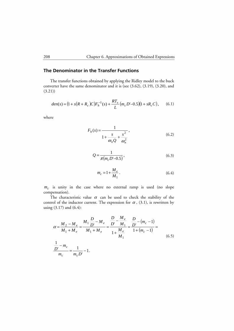
208 Chapter 6. Approximations of Obtained Expressions
The Denominator in the Transfer Functions
The transfer functions obtained by applying the Ridley model to the buck converter have the same denominator and it is (see (3.62), (3.19), (3.20), and (3.21))
( )( ) ( )( ) ,15.0')(1)( 1 CsRDmL
RTsFCRRssden cc
shc +−+++= − (6.1)
where
,
1
1)(
2
2
nn
hs
Q
ssF
ωω++
= (6.2)
( ) ,5.0'
1−
=Dm
Qcπ
(6.3)
.11M
Mm e
c += (6.4)
cm is unity in the case where no external ramp is used (no slope compensation).
The characteristic value α can be used to check the stability of the control of the inductor current. The expression for α , (3.1), is rewritten by using (3.17) and (6.4):
( )( )
.1'
1'
1
11
1'
1
''
1
1
1
1
1
2
−=−
=−+
−−=
+
−=
+
−=
+−
=
Dmm
mD
m
mD
D
M
MM
M
D
D
MM
MD
DM
MM
MM
cc
c
c
c
e
e
e
e
e
eα
(6.5)
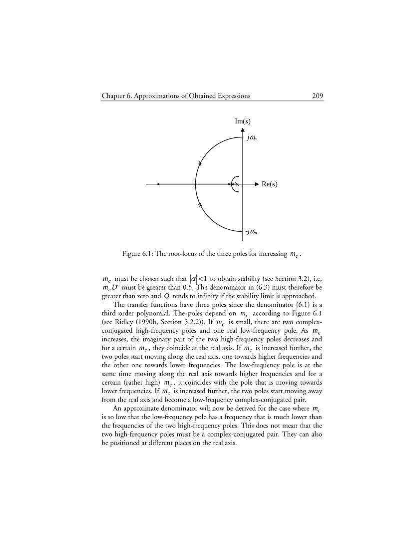
Chapter 6. Approximations of Obtained Expressions 209
Figure 6.1: The root-locus of the three poles for increasing cm .
cm must be chosen such that 1<α to obtain stability (see Section 3.2), i.e. 'Dmc must be greater than 0.5. The denominator in (6.3) must therefore be
greater than zero and Q tends to infinity if the stability limit is approached. The transfer functions have three poles since the denominator (6.1) is a
third order polynomial. The poles depend on cm according to Figure 6.1 (see Ridley (1990b, Section 5.2.2)). If cm is small, there are two complex-conjugated high-frequency poles and one real low-frequency pole. As cm increases, the imaginary part of the two high-frequency poles decreases and for a certain cm , they coincide at the real axis. If cm is increased further, the two poles start moving along the real axis, one towards higher frequencies and the other one towards lower frequencies. The low-frequency pole is at the same time moving along the real axis towards higher frequencies and for a certain (rather high) cm , it coincides with the pole that is moving towards lower frequencies. If cm is increased further, the two poles start moving away from the real axis and become a low-frequency complex-conjugated pair.
An approximate denominator will now be derived for the case where cm is so low that the low-frequency pole has a frequency that is much lower than the frequencies of the two high-frequency poles. This does not mean that the two high-frequency poles must be a complex-conjugated pair. They can also be positioned at different places on the real axis.
Re(s)
Im(s)
jωn
-jωn

210 Chapter 6. Approximations of Obtained Expressions
Assume that the ESR of the capacitor is much smaller than the resistance of the load, i.e.
.RRc << (6.6)
The denominator (6.1) can then be rewritten as:
( ) ( )( )
( ) ( )
( ) ,)(1
111
5.0'1
5.0'1
15.0'11)(
133
221
1
32
22
2
2
sPKsasasaK
sRCsQ
RC
sCRDmL
RTRC
QDm
L
RT
CsRDmL
RTs
Q
ssRCsden
nnn
ccs
nc
s
ccs
nn
−− =+++
=+
+
+
−+++−+
=+−+
+++≈
ωωω
ω
ωω
(6.7)
where
( ),
5.0'1
1
−+=
DmL
RTK
cs
(6.8)
,1)( 33
221 sasasasP +++= (6.9)
( ) ,5.0'11
1
−++= DmL
TRRC
QKa c
sc
nω(6.10)
,1
22
+=
Q
RCKa
nn ωω (6.11)
.23n
RCKa
ω= (6.12)
Chapter 6. Approximations of Obtained Expressions 211
The following derivation is similar to the one made by Erickson and Maksimovic (2000, Section 8.1.8). The polynomial )(sP is factored into
( )( )( )( ) ( )
( )( )( ) ,
1
111)(
313
12
11
213
12
13
11
12
11
13
12
11
13
12
11
sppp
sppppppsppp
spspspsP
−−−
−−−−−−−−−
−−−
−−−
++++−−−+
=−−−=
(6.13)
where 1p , 2p , and 3p are the three poles. The coefficient 1a is identified by using (6.9) and (6.13):
.13
12
111
−−− −−−= pppa (6.14)
As mentioned previously, the approximation will be made with the
assumption that the low-frequency pole has a frequency that is much lower than the frequencies of the two high-frequency poles. This means that
21 pp << and 31 pp << if 1p is the low-frequency pole. 1a is then approximated with
.111−−≈ pa (6.15)
An approximate expression for the (real) low-frequency pole is hence known. The polynomial )(sP is approximated with
( )( )( )( )( )
( ) ( ) .1
11
111)(
321
221111
2211
13
121
sbasbbasba
sbsbsa
spspsasP
+++++
=+++
=−−+≈ −−
(6.16)
The coefficients 1b and 2b are real since the poles 1p and 2p are either complex conjugated or real. Approximate expressions for 1b and 2b are obtained by comparing (6.9) and (6.16):
,1
32 a
ab ≈ (6.17)

212 Chapter 6. Approximations of Obtained Expressions
.
21
3
1
2
1
1
32
1
221
a
a
a
a
a
a
aa
a
bab −=
−≈
−≈
(6.18)
(6.16) is rewritten by using (6.17) and (6.18):
( ) .11)( 2
1
321
3
1
21
+
−++≈ s
a
as
a
a
a
asasP (6.19)
The denominator (6.7) is now approximated by using (6.19):
( ) .11)()( 2
1
321
3
1
21
11
+
−++≈≈ −− s
a
as
a
a
a
asaKsPKsden (6.20)
The following two assumptions are made before continuing:
( ) ,15.0' <<−DmL
TRc
sc (6.21)
.1
RCQn
<<ω
(6.22)
This means that 1a can be approximated with
.1 RCKa ≈ (6.23)
The denominator (6.20) is approximated by using (6.23), (6.11), and (6.12):
( )
.1111
1
1)(
2222
1
+
−++
•+≈ −
ssRCKQRC
RCKsKsden
nnnn ωωωω
(6.24)
One part of (6.24) is rewritten as follows by using (6.8), (3.13), and (6.3):

Chapter 6. Approximations of Obtained Expressions 213
( )
( )( )
,111
11
5.0'
1111
5.0'11
5.0'1111
11
11111
20
2
22
2
222
−=
−
=
−
−=−−
=
−+−+
=
−+=−+
nnnn
cs
nncs
nn
cs
nn
nnnnn
QLCQ
DmTLCQ
DmTLCQ
DmL
RT
RCQ
KRCQRCKQRC
ωω
ωωω
ππωωωω
ωω
ωωωωω
(6.25)
where
LC
10 =ω (6.26)
is the corner frequency of the output low-pass LC-filter (if the ESR in the capacitor is negligible). The corner frequency of this filter should be chosen to be much lower than the switching frequency to obtain small magnitude of the ripple in the output voltage (see Section 2.2). The following assumption is therefore also made:
.0 nωω << (6.27)
The denominator (6.24) can now be approximated by using (6.25) and (6.27):
( ) ,)(1)( 11 sFsRCKKsden h−− +≈ (6.28)
where )(sFh is defined in (6.2).
One of the assumptions used in the derivation of the approximate denominator (6.28) is that the low-frequency pole has a frequency that is much lower than the frequencies of the two high-frequency poles. Conditions that ensure that this assumption is fulfilled are derived in the following by utilization of the approximate denominator (6.28). It is a little unsatisfactory
214 Chapter 6. Approximations of Obtained Expressions
to utilize the expression for the approximate denominator to derive a condition that shows if the expression for the approximate denominator is valid. This is made anyway since the derivation then becomes rather simple.
In the approximate denominator (6.28), the low-frequency pole is equal to RCK1− and the two high-frequency poles are determined by )(sFh . In the case where the two high-frequency poles are complex conjugates, both of them have the frequency nω . The condition
nRCKω<<1
(6.29)
ensures that the low-frequency pole has a frequency that is much lower than the frequencies of the two high-frequency poles in this case. In the case where the two high-frequency poles are real, one of them has a frequency that is lower than (or equal to) nω . By putting the denominator in )(sFh equal to zero, it is concluded that the two high-frequency poles are real if and only if
5.0≤Q . The frequency of the pole with the lowest frequency can in this case be approximated with Qnω according to Erickson and Maksimovic (2000, Section 8.1.7). This pole is hence moving towards the low-frequency pole as Q is decreased. This is in accordance with Figure 6.1 since Q is decreasing if
cm is increasing (see (6.3)). It is concluded that the condition
QRCK nω<<1
(6.30)
ensures that the low-frequency pole has a frequency that is much lower than the frequencies of the two high-frequency poles in the case where the two high-frequency poles are real.
From (6.8), it is seen that K is a positive number less than unity since 'Dmc is greater than 0.5 if the current control is stable (see (6.5)). The
following is obtained if this result is combined with (6.30):
.1
RCRCKQn
<<<ω
(6.31)
Hence, the condition (6.30) ensures that the condition (6.22) is fulfilled.
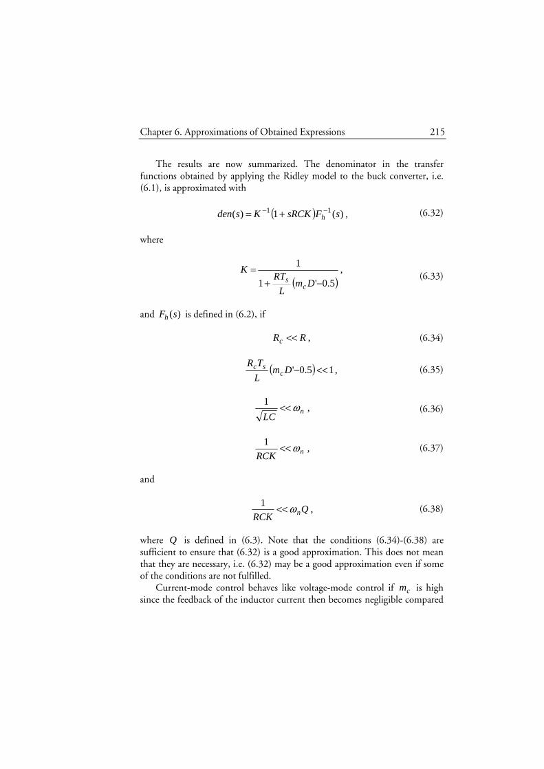
Chapter 6. Approximations of Obtained Expressions 215
The results are now summarized. The denominator in the transfer functions obtained by applying the Ridley model to the buck converter, i.e. (6.1), is approximated with
( ) ,)(1)( 11 sFsRCKKsden h−− += (6.32)
where
( ),
5.0'1
1
−+=
DmL
RTK
cs
(6.33)
and )(sFh is defined in (6.2), if
,RRc << (6.34)
( ) ,15.0' <<−DmL
TRc
sc (6.35)
,1
nLC
ω<< (6.36)
,1
nRCKω<< (6.37)
and
,1
QRCK nω<< (6.38)
where Q is defined in (6.3). Note that the conditions (6.34)-(6.38) are sufficient to ensure that (6.32) is a good approximation. This does not mean that they are necessary, i.e. (6.32) may be a good approximation even if some of the conditions are not fulfilled.
Current-mode control behaves like voltage-mode control if cm is high since the feedback of the inductor current then becomes negligible compared
216 Chapter 6. Approximations of Obtained Expressions
Figure 6.2: The denominator in the transfer functions for a buck converter with a current controller. Dashed line: the approximated denominator. Solid line: the Ridley model. Note that the two lines almost coincide.
to the external ramp (compare Figure 3.3 and Figure 3.4). In voltage-mode control, there is a resonance frequency at approximately LC1 . This is predicted by the denominator (6.1) since it has two low-frequency complex-conjugated poles for high cm . However, the approximate denominator (6.32) does not predict this since it only has real poles for high cm .
The Bode plots for the denominators (6.1) and (6.32) are shown in Figure 6.2. The parameter values shown in Table 2.1 are used. From the figure it is seen that the two denominators are almost the same. The maximum difference is approximately 0.1 dB and 0.3 degrees in the presented frequency interval.
Control-to-Output Transfer Function
An approximate version of the control-to-output transfer function obtained by applying the Ridley model to the buck converter is
101
102
103
104
0
10
20
30
40
50
101
102
103
104
0
50
100
150
200
Frequency (Hz)
Pha
se (
deg)
; M
agni
tude
(dB
)
Chapter 6. Approximations of Obtained Expressions 217
( )
,)(
1
)(ˆ)(ˆ
sden
CsRR
si
sv c
c
o += (6.39)
where )(sden is defined in (6.32) if the conditions in (6.34)-(6.38) are fulfilled. The only difference compared to the non-approximated version (3.59) is that the approximate denominator (6.32) is used instead of the denominator (6.1).
(6.39) is rewritten by using (6.32):
( )
( ),)()()(
)(1
1
)(ˆ)(ˆ
11sFsFsRKF
sFsRCKK
CsRR
si
svhESRl
h
c
c
o =+
+= −− (6.40)
where
,1
1)(
sRCKsFl +
= (6.41)
,1)( CsRsF cESR += (6.42)
)(sFh is defined in (6.2), and K is defined in (6.33). (6.40) is exactly the
same as the approximate control-to-output transfer function proposed by Ridley (1991).
Output Impedance
An approximate version of the output impedance obtained by applying the Ridley model to the buck converter is
( )
,)(
)(1)(
1
sden
sFCsRRsZ hc
out
−+= (6.43)
where )(sden is defined in (6.32) and )(sFh is defined in (6.2) if the conditions in (6.34)-(6.38) are fulfilled. The only difference compared to the non-approximated version (3.60) is that the approximate denominator (6.32) is used instead of the denominator (6.1).
(6.43) is rewritten by using (6.32):
218 Chapter 6. Approximations of Obtained Expressions
( )( )
,)()()(1
)(1)(
11
1
sFsRKFsFsRCKK
sFCsRRsZ ESRl
h
hcout =
++
= −−
− (6.44)
where K is defined in (6.33), )(sFl is defined in (6.41), and )(sFESR is defined in (6.42). The two high-frequency poles are cancelled by two of the zeros. (6.44) is exactly the same as the approximate output impedance proposed by Ridley (1991).
Audio Susceptibility
In this subsection, the audio susceptibilities obtained by applying the Ridley model and the improved Ridley model to the buck converter are approximated. The expression )(sF f , used in the numerator of the improved expression for the audio susceptibility, is approximated in two different ways. The first one is by using a Taylor polynomial and the second one is by minimizing an integral.
An approximate version of the audio susceptibility obtained by applying the Ridley model to the buck converter is
( )
,)(
12
1'
)(ˆ
)(ˆ
sden
CsRD
DmDL
RT
sv
svcc
s
g
o
+
−−
=(6.45)
where )(sden is defined in (6.32) if the conditions in (6.34)-(6.38) are fulfilled. The only difference compared to the non-approximated version (3.61) is that the approximate denominator (6.32) is used instead of the denominator (6.1).
(6.45) is rewritten by using (6.32):
( )
( )
,)()()(2
1'
)(1
12
1'
)(ˆ
)(ˆ11
sFsFsKFD
DmL
DRT
sFsRCKK
CsRD
DmDL
RT
sv
sv
hESRlcs
h
ccs
g
o
−−
=+
+
−−= −− (6.46)
Chapter 6. Approximations of Obtained Expressions 219
where K is defined in (6.33), )(sFl is defined in (6.41), )(sFESR is defined in (6.42), and )(sFh is defined in (6.2). (6.46) is exactly the same as the approximate audio susceptibility proposed by Ridley (1991).
The expression for the audio susceptibility obtained by applying the Ridley model to the buck converter was improved in Chapter 5 by replacing the numerator (see (5.9)). An approximate version of this improved expression is
( )( )( )
( ) ,)()()()('
)(1
1)('
)(ˆ
)(ˆ11
sFsFsKFsFDmL
DRT
sFsRCKK
CsRsFDmDL
RT
sv
sv
hESRlfcs
h
cfcs
g
o
−
=+
+−= −− (6.47)
where
( ) ( )
K++−
−−
−
−
=
−−−
−=
−
−
222
24
21
12
23
21
1
1
1
1)(
sDTDD
sDTDD
e
sT
sDT
e
e
sT
sTsF
ss
sTs
s
sDT
sTs
sf
s
s
s
(6.48)
(see (4.27)), K is defined in (6.33), )(sFl is defined in (6.41), )(sFESR is defined in (6.42), and )(sFh is defined in (6.2) if the conditions in (6.34)-(6.38) are fulfilled.
Since )(sF f is a rather complicated expression, it is desirable to find an approximate expression. )(sF f can be approximated by a Taylor polynomial, i.e. a truncated version of the Taylor series in (6.48). The higher degree of the Taylor polynomial that is used, the better approximation is obtained. If a Taylor polynomial of degree 0 is used, )(sk f in (5.10) is the same as fk in (5.3) and the Ridley model is not improved. This is also seen if (6.46) and (6.47) are compared. If a Taylor polynomial of degree 1 is used, there is an extra zero in the improved Ridley model. In Section 3.4, it was observed that the Tan model includes an extra zero compared to the Ridley model (compare (3.61) and (3.71)). If a Taylor polynomial of degree 1 is used to improve the Tan model, the extra zero that is already present in the Tan model, is moved to a more suitable position. The extra zero in the Tan model
220 Chapter 6. Approximations of Obtained Expressions
explains why the Tan model is better than the Ridley model in Figure 4.14. However, the Ridley model is better than the Tan model in some cases since the extra zero in the Tan model is not placed at the most suitable position. This is for instance the case if D is small. If D tend to zero, )(sF f in (6.48) tend to 1 and 21 D− in the numerator of (6.46) also tend to 1. The Ridley model therefore becomes the same as the improved version of the Ridley model. However, in the Tan model the extra zero remains, which can be concluded from (3.71). s is equal to the extra zero if
.02
1' =+
−−
nc
sDDm
πω (6.49)
(6.49) is rewritten:
.2
11
21'
−−−−=
−−−= ccncn mDm
DDms πωπω (6.50)
It is seen from (6.50) that the extra zero does not disappear (move to infinity) as D tend to zero.
Figure 6.3 is a modified version of Figure 4.14. It shows the Bode plot for the audio susceptibility predicted by the Ridley model (3.61) together with the simulation results. It also shows the audio susceptibilities predicted by the improved Ridley model ((3.58) with fk replaced by )(sk f in (5.10)) in the cases where )(sF f is not approximated, )(sF f is approximated by a Taylor polynomial of degree 1 and 2. From the figure it is seen that the predictions of the improved Ridley model agree more closely with the simulation results if the degree of the Taylor polynomial is increased.
A Taylor polynomial approximates a function in a neighborhood of a point. There are other methods that approximate a function in an interval. The rest of this section will be devoted to an example of how )(sF f can be approximated in the frequency interval dc to half the switching frequency,
nω . This example can be omitted by the reader without risk of increasing difficulty to understand subsequent sections of this thesis.
Let the function )(zg be defined by (see (6.48))
.1
1
1
1)(
−−−
−=
=
−
− z
zD
zs
fe
z
zD
e
e
z
zT
zFzg (6.51)

Chapter 6. Approximations of Obtained Expressions 221
Figure 6.3: The audio susceptibility of a buck converter with a current controller ( cm =1.5). X: the simulation results. Solid line: the Ridley model. Dashed line: the improved Ridley model with
)(sF f approximated by a Taylor polynomial of degree 1. Dash-dotted line: the improved Ridley model with )(sF f approximated by a Taylor polynomial of degree 2. Dotted line: the improved Ridley model with )(sF f not approximated.
Note that the complex variable z is not connected with the Z-transform in this chapter. )(zg will be approximated and an approximation of )(sF f is then obtained by
.)()( sf sTgsF = (6.52)
Let ωjs = . If nωω ≤≤0 , then ssT is in the interval [ ]snTjω,0 which is rewritten as [ ]πj,0 by using (3.13). )(zg should therefore be approximated for z in the interval [ ]πj,0 .
One way of approximating a function )(zf on a curve C is to use the method of least squares and the result is (Walsh, 1935, Section 6.1):
101
102
103
104
-80
-70
-60
-50
-40
-30
101
102
103
104
-150
-100
-50
0
Frequency (Hz)
Pha
se (
deg)
; M
agni
tude
(dB
)
222 Chapter 6. Approximations of Obtained Expressions
.)()()()( 1100 zpazpazpazf nn+++≈ K (6.53)
where
,)()(∫=C
kk dzzpzfa (6.54)
and the functions )(0 zp , )(1 zp , K , )(zpn are normal and orthogonal on C . The coefficients ka in (6.54) minimizes the integral
.)()(
2
0∫ ∑
=−
C
n
kkk dzzpazf (6.55)
The function )(zg is approximated by using (6.53) and (6.54). The
curve C is chosen to be the part of the imaginary axis that starts at the origin and ends at πj . A set of functions, )(0 zp , )(1 zp , K , )(zpn , that are normal and orthogonal on C must also be found. It is seen from (6.55) that the approximation error is equally weighed for each z in C . It is possible to reduce the approximation error for some z by introducing a weight function. The approximation error will then increase for other z . Another possibility is to introduce a special condition and then reformulate the approximation problem so that the condition is fulfilled. If the special condition is that the approximation error should be zero for z =0 (dc), then the reformulated approximation problem is to approximate the function )(zf defined by
.)0()(
)(z
gzgzf
−= (6.56)
)(zg is then obtained by
.)()0()( zzfgzg += (6.57)
It is seen from (6.57) that the approximation error equals zero for z =0. If )(zf in (6.56) is approximated by using (6.53) and (6.54) and the
functions )(0 zp , )(1 zp , K , )(zpn are polynomials, then the approximated )(zf is also a polynomial. The coefficients in this polynomial are complex numbers. It will now be shown how )(zf can be approximated
Chapter 6. Approximations of Obtained Expressions 223
by a polynomial of degree 1 where the coefficients are restricted to be real numbers. Note that this approximation will not be as good as the case where complex coefficients are allowed. )(zf is approximated by the polynomial
.10 zλλ + (6.58)
The values of the real coefficients 0λ and 1λ are obtained by minimizing the integral
( ) ( )
( )( )
()
( )
( ) .3
)()(
)()()()(
)(
)()()()()(
)()(
)()(
321
20
01
00
0
22101110
20
0010
01010
0
210
0
210
πλπλθθθθθλ
θθθλθθθ
θθλθλλθθλθλλλ
θλθλθλθθθ
θθλλθθλλθ
θθλλθλλ
π
ππ
π
π
ππ
+++−
−+−
=++−−
+−+−
=−−−−
=+−=+−
∫
∫∫
∫
∫
∫∫
djfjjfj
djfjfdjfjf
djjfjj
jfjjfjfjfjf
djjfjjf
djjfdzzzfj
(6.59)
Define the following:
( ) ,)()(2
1
00 ∫ +=
πθθθ
πdjfjfa (6.60)
( ) .)()(2
3
031 ∫ +−=
πθθθθθ
πdjfjjfja (6.61)
(6.59) is rewritten by using (6.60) and (6.61);
224 Chapter 6. Approximations of Obtained Expressions
( )
( ) ( ) .33
)()(
33
33
22)()(
)(
21
320
211
32
000
21
321
320
20
321
201
3
1000
0
210
aaaadjfjf
aaaa
aadjfjf
dzzzfj
ππλπλπθθθ
ππππ
πλπλπλπλθθθ
λλ
π
π
π
−−−+−+
=−+−
+++−−
=+−
∫
∫
∫
(6.62)
It is seen from (6.62) that the minimum is obtained if 0λ is equal to 0a and
1λ is equal to 1a . It is also seen that if )(zf should be approximated by a polynomial of degree 0, i.e. 1λ =0, then 0λ should still be set equal to 0a to obtain the minimum. (6.60) and (6.61) are rewritten:
( ) ,)(Re1
00 ∫=
πθθ
πdjfa (6.63)
( ) ( )
( ) ( )( )( )
( ) ( ) .)(Im3
)(Im3
)(Im)(ReRe3
)(Re3
)()(2
3
03
03
03
03
031
∫∫
∫
∫∫
=
=+−
=−=+−=
ππ
π
ππ
θθθπ
θθθπ
θθθθθπ
θθθπ
θθθθθπ
djfdjf
djfjjfj
djfjdjfjjfja
(6.64)
The conclusion is that the function )(zf in (6.56) can be approximated by the first order polynomial
,)( 10 zaazf +≈ (6.65)
where 0a is defined in (6.63) and 1a is defined in (6.64). )(zf can also be approximated by the zeroth order polynomial
Chapter 6. Approximations of Obtained Expressions 225
,)( 0azf ≈ (6.66)
where 0a is defined in (6.63). Note that 0a and 1a are real numbers. )0(g is calculated by application of (6.51) and (6.48):
( ) .2
10)0(D
Fg f −== (6.67)
From (6.52), (6.57), and (6.67), )(sF f is written as
.)(2
1)()0()()( sssssf sTfsTD
sTfsTgsTgsF +
−=+== (6.68)
)(sF f can now be approximated with
22102
1)( sTasTaD
sF ssf ++
−≈ (6.69)
(by using (6.68) and (6.65)) or
sTaD
sF sf 021)( +
−≈ (6.70)
(by using (6.68) and (6.66)), where
( ) ,)(Re1
00 ∫=
πθθ
πdjfa (6.71)
( ) .)(Im3
031 ∫=
πθθθ
πdjfa (6.72)
)( θjf in (6.71) and (6.72) is obtained by using (6.56), (6.67), and (6.51):

226 Chapter 6. Approximations of Obtained Expressions
Figure 6.4: Calculated value of 0a for different values of D .
.2
11
1
1
1
21)(
)0()()(
θ
θθ
θθ
θ
θ
θθθ
θ
θ
θ
j
D
e
j
Dj
e
e
j
j
j
Djg
j
gjgjf
j
Dj
j
−−
−−−
−
=
−−=−=
−
−
(6.73)
The integrals in (6.71) and (6.72) must be solved numerically. The lower
integration limit must be increased to a small positive number since there will be divisions with zero if θ is set to zero in )( θjf . It is seen from (6.73) that
)( θjf depends on D , i.e. the operating-point value of the duty cycle. 0a and 1a therefore also depend on D . 0a and 1a are calculated for 1000 different values of D in the interval ] ]1,0 . The results are plotted in Figure 6.4 and Figure 6.5.
0 0.1 0.2 0.3 0.4 0.5 0.6 0.7 0.8 0.9 1
-0.1
-0.09
-0.08
-0.07
-0.06
-0.05
-0.04
-0.03
-0.02
-0.01
0
D
a0

Chapter 6. Approximations of Obtained Expressions 227
Figure 6.5: Calculated value of 1a for different values of D . A polynomial curve is fitted to the 1000 values plotted in Figure 6.4 by
utilization of the method of least squares. An approximate expression for 0a is obtained:
.01654.015370.025892.000046.0 320 DDDa ++−≈ (6.74)
The same is made for the values plotted in Figure 6.5 and an approximate expression for 1a is:
.04892.009816.004933.000012.0 321 DDDa −+−≈ (6.75)
Figure 6.6 is a modified version of Figure 6.3. It shows the Bode plot for
the audio susceptibility predicted by the Ridley model (3.61) together with the simulation results. It also shows the audio susceptibilities predicted by the improved Ridley model ((3.58) with fk replaced by )(sk f in (5.10)) in the cases where )(sF f is not approximated, )(sF f is approximated by (6.70),
0 0.1 0.2 0.3 0.4 0.5 0.6 0.7 0.8 0.9 1-0.008
-0.007
-0.006
-0.005
-0.004
-0.003
-0.002
-0.001
0
D
a1
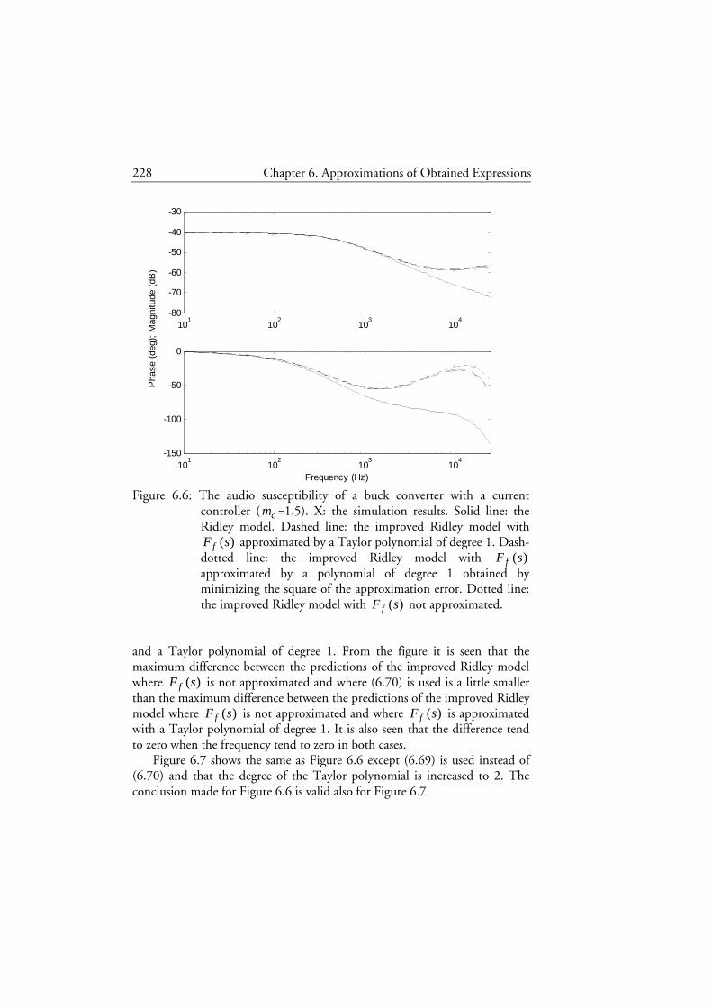
228 Chapter 6. Approximations of Obtained Expressions
Figure 6.6: The audio susceptibility of a buck converter with a current controller ( cm =1.5). X: the simulation results. Solid line: the Ridley model. Dashed line: the improved Ridley model with
)(sF f approximated by a Taylor polynomial of degree 1. Dash-dotted line: the improved Ridley model with )(sF f approximated by a polynomial of degree 1 obtained by minimizing the square of the approximation error. Dotted line: the improved Ridley model with )(sF f not approximated.
and a Taylor polynomial of degree 1. From the figure it is seen that the maximum difference between the predictions of the improved Ridley model where )(sF f is not approximated and where (6.70) is used is a little smaller than the maximum difference between the predictions of the improved Ridley model where )(sF f is not approximated and where )(sF f is approximated with a Taylor polynomial of degree 1. It is also seen that the difference tend to zero when the frequency tend to zero in both cases.
Figure 6.7 shows the same as Figure 6.6 except (6.69) is used instead of (6.70) and that the degree of the Taylor polynomial is increased to 2. The conclusion made for Figure 6.6 is valid also for Figure 6.7.
101
102
103
104
-80
-70
-60
-50
-40
-30
101
102
103
104
-150
-100
-50
0
Frequency (Hz)
Pha
se (
deg)
; M
agni
tude
(dB
)
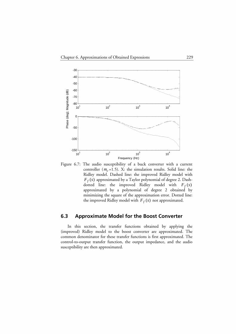
Chapter 6. Approximations of Obtained Expressions 229
Figure 6.7: The audio susceptibility of a buck converter with a current controller ( cm =1.5). X: the simulation results. Solid line: the Ridley model. Dashed line: the improved Ridley model with
)(sF f approximated by a Taylor polynomial of degree 2. Dash-dotted line: the improved Ridley model with )(sF f approximated by a polynomial of degree 2 obtained by minimizing the square of the approximation error. Dotted line: the improved Ridley model with )(sF f not approximated.
6.3 Approximate Model for the Boost Converter
In this section, the transfer functions obtained by applying the (improved) Ridley model to the boost converter are approximated. The common denominator for these transfer functions is first approximated. The control-to-output transfer function, the output impedance, and the audio susceptibility are then approximated.
101
102
103
104
-80
-70
-60
-50
-40
-30
101
102
103
104
-150
-100
-50
0
Frequency (Hz)
Pha
se (
deg)
; M
agni
tude
(dB
)

230 Chapter 6. Approximations of Obtained Expressions
The Denominator in the Transfer Functions
The transfer functions obtained by applying the Ridley model to the boost converter have the same denominator and it is (see (3.95), (3.35), and (3.12))
( )( )
( ) ( )
( ) ,'
'
'
'2)(
'11
2
'
1'
''
)(
22
3
+++
+
+
+−+
−
+++
+
+++
=
RD
RRDCRRs
RD
RRDsH
DR
LRRsCsR
L
TRD
CRRssLCsRRR
RRDRD
R
RRD
L
mT
sden
cc
ce
cc
s
ccc
cccs
(6.76)
where
,1)(2
2
nzne
s
Q
ssH
ωω++= (6.77)
.2
π−=zQ (6.78)
An approximate denominator will now be derived for the case where cm
is so low that the low-frequency pole has a frequency that is much lower than the frequencies of the two high-frequency poles.
Assume that
.'RDRc << (6.79)
Since 'D is a positive number less than or equal to unity, the following is obtained by using (6.79):
.' RRDRc ≤<< (6.80)
The denominator (6.76) is rewritten by using (6.80) and (3.54):

Chapter 6. Approximations of Obtained Expressions 231
( ) ( )( )
( )
( )
( ) ,)(11
'12
2
''
'22
2
'
2
'''
22
''
2'1
'11
2
'
1''')(
133
221
132
22
32
33
2
2
2
3
sPKsasasaKRCs
sRCDmTRCQ
CRTD
LRCDL
mT
sRCDmTQ
TD
CRL
TRDDmTCRRD
L
mT
L
TRDRD
L
mT
sRCDmsTs
Q
s
RD
LsCsR
L
TRD
sRCsLCsRDRDDL
mTsden
n
csnn
cscs
csn
s
cs
csccs
scs
csnn
cs
ccs
−− =+++=
+
−+++
+
+−+
+
−+
++−
=+
−++
+
−+
−+++≈
ω
ωω
ω
ωω
(6.81)
where
( ),
5.0'
2
13
−+=
cs m
L
TRDK
(6.82)
,1)( 33
221 sasasasP +++= (6.83)
( ) ,5.0'2
''1
2 2
1
−−
−++= csc
sc
n
mTDD
mL
TDRRC
QKa
ω (6.84)
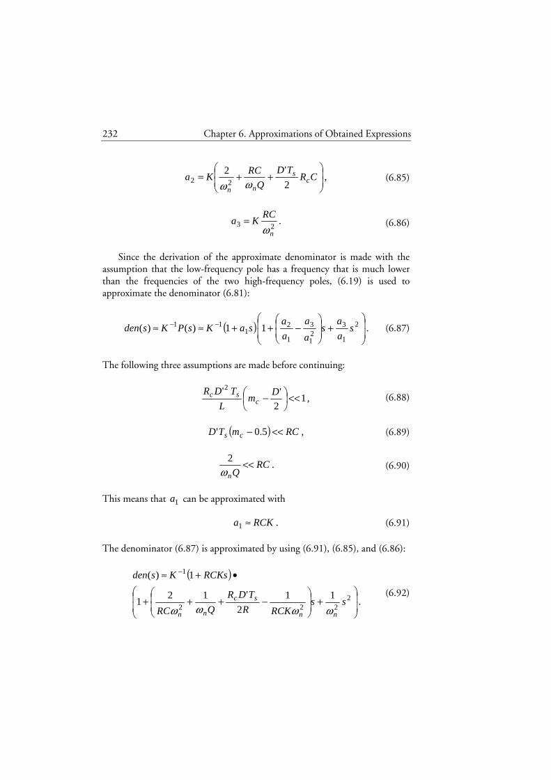
232 Chapter 6. Approximations of Obtained Expressions
,2
'222
++= CR
TD
Q
RCKa c
s
nn ωω (6.85)
.23n
RCKa
ω= (6.86)
Since the derivation of the approximate denominator is made with the
assumption that the low-frequency pole has a frequency that is much lower than the frequencies of the two high-frequency poles, (6.19) is used to approximate the denominator (6.81):
( ) .11)()( 2
1
321
3
1
21
11
+
−++≈≈ −− s
a
as
a
a
a
asaKsPKsden (6.87)
The following three assumptions are made before continuing:
,12
''2<<
− D
mL
TDRc
sc (6.88)
( ) ,5.0' RCmTD cs <<− (6.89)
.2
RCQn
<<ω
(6.90)
This means that 1a can be approximated with
.1 RCKa ≈ (6.91)
The denominator (6.87) is approximated by using (6.91), (6.85), and (6.86):
( )
.11
2
'121
1)(
2222
1
+
−+++
•+≈ −
ssRCKR
TDR
QRC
RCKsKsden
nn
sc
nn ωωωω
(6.92)
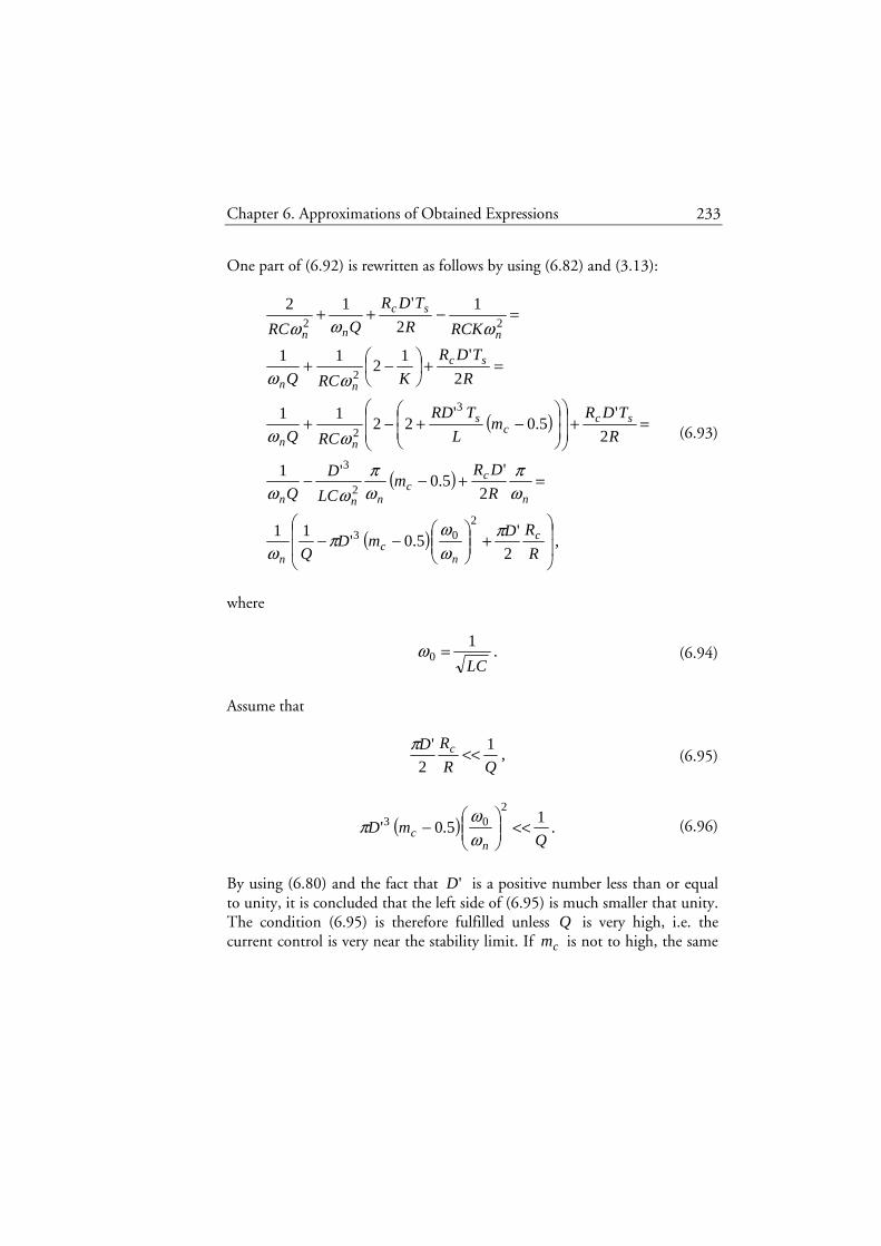
Chapter 6. Approximations of Obtained Expressions 233
One part of (6.92) is rewritten as follows by using (6.82) and (3.13):
( )
( )
( ) ,2
'5.0'
11
2
'5.0
'1
2
'5.0
'22
11
2
'12
11
1
2
'12
203
2
3
3
2
2
22
+
−−
=+−−
=+
−+−+
=+
−+
=−++
R
RDmD
Q
R
DRm
LC
D
Q
R
TDRm
L
TRD
RCQ
R
TDR
KRCQ
RCKR
TDR
QRC
c
nc
n
n
cc
nnn
scc
s
nn
sc
nn
n
sc
nn
πωωπ
ω
ωπ
ωπ
ωω
ωω
ωω
ωωω
(6.93)
where
.1
0LC
=ω (6.94)
Assume that
,1
2
'
QR
RD c <<π (6.95)
( ) .1
5.0'2
03
QmD
nc <<
−
ωωπ (6.96)
By using (6.80) and the fact that 'D is a positive number less than or equal to unity, it is concluded that the left side of (6.95) is much smaller that unity. The condition (6.95) is therefore fulfilled unless Q is very high, i.e. the current control is very near the stability limit. If cm is not to high, the same

234 Chapter 6. Approximations of Obtained Expressions
is true also for condition (6.96) since 0ω usually is much lower than nω . The denominator (6.92) is approximated by using (6.93), (6.95), and (6.96):
( ) ,)(1)( 11 sFsRCKKsden h−− +≈ (6.97)
where )(sFh is defined in (6.2).
One of the assumptions used in the derivation of the approximate denominator (6.97) is that the low-frequency pole has a frequency that is much lower than the frequencies of the two high-frequency poles. Conditions that ensure that this assumption is fulfilled are (6.29) and (6.30), i.e. the conditions derived for the buck converter. The same conditions can be used for the boost converter since the approximate denominators are exactly the same (see (6.28) and (6.97)) except for the definition of K .
From (6.82), it is seen that K is a positive number less than 0.5. The following is obtained if this result is combined with (6.30):
.22
RCRCKQn
<<<ω
(6.98)
Hence, the condition (6.30) ensures that the condition (6.90) is fulfilled.
The results are now summarized. The denominator in the transfer functions obtained by applying the Ridley model to the boost converter, i.e. (6.76), is approximated with
( ) ,)(1)( 11 sFsRCKKsden h−− += (6.99)
where
( ),
5.0'
2
13
−+=
cs m
L
TRDK
(6.100)
and )(sFh is defined in (6.2), if
,'RDRc << (6.101)

Chapter 6. Approximations of Obtained Expressions 235
,12
''2<<
− D
mL
TDRc
sc (6.102)
( ) ,5.0' RCmTD cs <<− (6.103)
,1
2
'
QR
RD c <<π (6.104)
( ) ,11
5.0'
23
Q
LCmD
nc <<
−
ωπ (6.105)
,1
nRCKω<< (6.106)
and
,1
QRCK nω<< (6.107)
where Q is defined in (6.3).
The Bode plots for the denominators (6.76) and (6.99) are shown in Figure 6.8. The parameter values shown in Table 2.5 are used. From the figure it is seen that the two denominators are almost the same. The maximum difference is approximately 0.3 dB and 2 degrees in the presented frequency interval.
Control-to-Output Transfer Function
An approximate version of the control-to-output transfer function obtained by applying the Ridley model to the boost converter is
( )
,)(
'11'
)(ˆ)(ˆ 2
sdenRD
LsCsRRD
si
sv c
c
o
−+
= (6.108)

236 Chapter 6. Approximations of Obtained Expressions
Figure 6.8: The denominator in the transfer functions for a boost converter with a current controller. Dashed line: the approximated denominator. Solid line: the Ridley model. Note that the two lines almost coincide.
where )(sden is defined in (6.99) if the conditions in (6.101)-(6.107) are fulfilled. The only differences compared to the non-approximated version (3.92) are that the approximate denominator (6.99) is used instead of the denominator (6.76) and that (6.101) (which gives (6.80)) is used to approximate the numerator.
(6.108) is rewritten by using (6.99):
( )
( ),)()()()('
)(1
'11'
)(ˆ)(ˆ
11
2
sFsFsFsKFRD
sFsRCKK
RD
LsCsRRD
si
sv
RHPhESRl
h
c
c
o =+
−+
= −− (6.109)
where
101
102
103
104
0
10
20
30
40
50
101
102
103
104
0
50
100
150
200
Frequency (Hz)
Pha
se (
deg)
; M
agni
tude
(dB
)

Chapter 6. Approximations of Obtained Expressions 237
,1
1)(
sRCKsFl +
= (6.110)
,'
1)(2RD
LssFRHP −= (6.111)
)(sFESR is defined in (6.42), )(sFh is defined in (6.2), and K is defined in
(6.100).
Output Impedance
The output impedance obtained by applying the Ridley model to the boost converter is given by (3.93). The numerator in (3.93) will first be approximated. By using (6.101) (which gives (6.80)) and the fact that D is a positive number less than or equal to unity, the following is obtained:
.' RRDRDRR
RDR cc
cc ≤<<≤<< (6.112)
The numerator in (3.93) is approximated by using (6.112):
( )
.''
'1
1)(
2
2
2
22
+++++
•+=
DmsTs
Q
s
DR
DR
L
RDDmT
CsRRsnum
csnzn
cccs
c
ωω (6.113)
One part of (6.113) is approximated by using (2.39) and (6.112):
( )
( ) .''
1
'1'
'
'
'
'1
2
2
2
22
DmmL
TDR
DmL
TDR
RDR
RDRRD
DR
DR
L
RDDmT
ccsc
csc
cc
cccs
−+
≈−++
=++
(6.114)

238 Chapter 6. Approximations of Obtained Expressions
The second term in (6.114) is approximated by using (6.102) and the fact that cm is a positive number greater than or equal to unity:
( ) .1'2
1''
' 22
<<
−≤− Dm
L
TDRDmm
L
TDRc
sccc
sc (6.115)
Hence, (6.114) is approximately equal to unity. The numerator (6.113) can therefore be approximated with:
( ) )(1)( 1 sFCsRRsnum hc−+≈ (6.116)
according to (3.54).
An approximate version of the output impedance obtained by applying the Ridley model to the boost converter is
( )
,)(
)(1)(
1
sden
sFCsRRsZ hc
out
−+= (6.117)
where )(sden is defined in (6.99) and )(sFh is defined in (6.2) if the conditions in (6.101)-(6.107) are fulfilled. The only differences compared to the non-approximated version (3.93) are that the approximate denominator (6.99) is used instead of the denominator (6.76) and that the approximate numerator (6.116) is used instead of the numerator in (3.93).
(6.117) is rewritten by using (6.99):
( )( )
,)()()(1
)(1)(
11
1
sFsRKFsFsRCKK
sFCsRRsZ ESRl
h
hcout =
++
= −−
− (6.118)
where K is defined in (6.100), )(sFl is defined in (6.110), and )(sFESR is defined in (6.42). The two high-frequency poles are cancelled by two of the zeros.
Audio Susceptibility
The expression for the audio susceptibility obtained by applying the Ridley model to the boost converter was improved in Chapter 5 by replacing

Chapter 6. Approximations of Obtained Expressions 239
the numerator (see (5.24)). The improved expression then became the same as the combined expression (5.21). An approximate version of the improved expression is
( ) ( )
,)(
1'
1)(''
)(ˆ
)(ˆ
sden
CsRD
sFDmDL
RT
sv
sv cfcs
g
o
+
+−
= (6.119)
where
K++−=−
−= 33
720122
1
1
11)( s
Ts
T
esTsF ss
sTs
fs
(6.120)
(see (4.36)) and )(sden is defined in (6.99) if the conditions in (6.101)-(6.107) are fulfilled. The only differences compared to the non-approximated improved version (5.21) are that the approximate denominator (6.99) is used instead of the denominator (6.76) and that (6.101) (which gives (6.80)) is used to approximate the numerator.
(6.119) is rewritten by using (6.99):
( ) ( )
( )
( ) ,)()()('
1)('
'
)(1
1'
1)(''
)(ˆ
)(ˆ11
sFsFsKFD
sFDmL
DRT
sFsRCKK
CsRD
sFDmDL
RT
sv
sv
hESRlfcs
h
cfcs
g
o
+−
=+
+
+−
=−− (6.121)
where )(sF f is defined in (6.120), K is defined in (6.100), )(sFl is defined in (6.110), )(sFESR is defined in (6.42), and )(sFh is defined in (6.2).
)(sk f defined in (5.27) will now be approximated. )(sk f is first approximated by using (6.101) (which gives (6.80)):
,'
12
1'
)(22
)(1
22
−
−
−−−≈
RD
Lss
RD
LssF
L
RTsk
nf
isf πω
(6.122)

240 Chapter 6. Approximations of Obtained Expressions
Figure 6.9: The audio susceptibility of a boost converter with a current controller. X: the simulation results. Solid line: the Ridley model. Dashed line: the improved Ridley model with )(sF f approximated by a Taylor polynomial of degree 0. Dash-dotted line: the improved Ridley model with )(sF f approximated by a Taylor polynomial of degree 1. Dotted line: the improved Ridley model with )(sF f not approximated. Note that the solid and dashed lines coincide and that the dash-dotted and dotted lines almost coincide in the phase shift plot. Note also that the dashed, dash-dotted, and dotted lines almost coincide in the magnitude plot.
where )(sF f is defined in (6.120). A second step to approximate )(sk f is to approximate )(sF f .
)(sF f is approximated by a Taylor polynomial, i.e. a truncated version of the Taylor series in (6.120). Figure 6.9 is a modified version of Figure 5.3. It shows the Bode plot for the audio susceptibility predicted by the Ridley model (3.94) together with the simulation results. It also shows the audio susceptibilities predicted by the improved Ridley model ((3.91) with fk replaced by )(sk f in (5.27)) in the cases where )(sF f is not approximated,
101
102
103
104
-60
-40
-20
0
101
102
103
104
-150
-100
-50
0
Frequency (Hz)
Pha
se (
deg)
; M
agni
tude
(dB
)
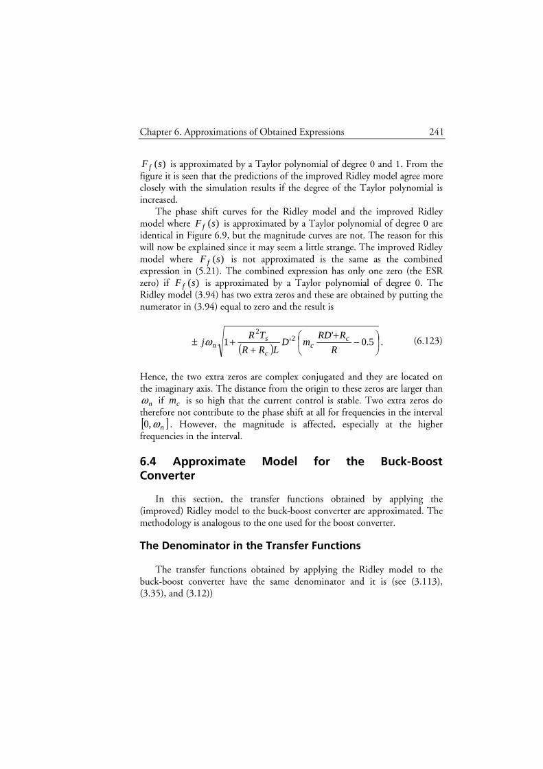
Chapter 6. Approximations of Obtained Expressions 241
)(sF f is approximated by a Taylor polynomial of degree 0 and 1. From the figure it is seen that the predictions of the improved Ridley model agree more closely with the simulation results if the degree of the Taylor polynomial is increased.
The phase shift curves for the Ridley model and the improved Ridley model where )(sF f is approximated by a Taylor polynomial of degree 0 are identical in Figure 6.9, but the magnitude curves are not. The reason for this will now be explained since it may seem a little strange. The improved Ridley model where )(sF f is not approximated is the same as the combined expression in (5.21). The combined expression has only one zero (the ESR zero) if )(sF f is approximated by a Taylor polynomial of degree 0. The Ridley model (3.94) has two extra zeros and these are obtained by putting the numerator in (3.94) equal to zero and the result is
( ) .5.0
''1 2
2
−+
++±
R
RRDmD
LRR
TRj c
cc
snω (6.123)
Hence, the two extra zeros are complex conjugated and they are located on the imaginary axis. The distance from the origin to these zeros are larger than
nω if cm is so high that the current control is stable. Two extra zeros do therefore not contribute to the phase shift at all for frequencies in the interval [ ]nω,0 . However, the magnitude is affected, especially at the higher frequencies in the interval.
6.4 Approximate Model for the Buck-Boost Converter
In this section, the transfer functions obtained by applying the (improved) Ridley model to the buck-boost converter are approximated. The methodology is analogous to the one used for the boost converter.
The Denominator in the Transfer Functions
The transfer functions obtained by applying the Ridley model to the buck-boost converter have the same denominator and it is (see (3.113), (3.35), and (3.12))
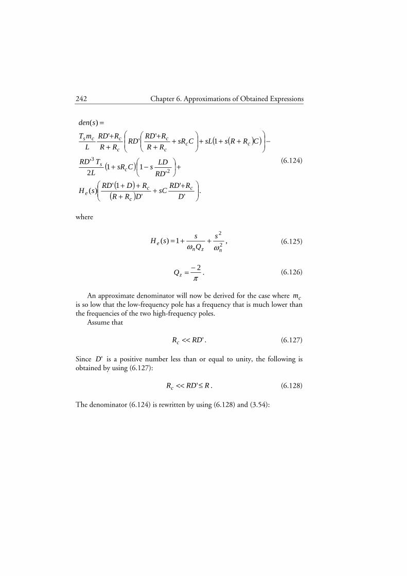
242 Chapter 6. Approximations of Obtained Expressions
( )( )
( )
( )( ) .
'
'
'
1')(
'11
2
'
1'
''
)(
2
3
++
+++
+
−+
−
+++
+
++
++
=
D
RRDsC
DRR
RDRDsH
RD
LDsCsR
L
TRD
CRRssLCsRRR
RRDRD
RR
RRD
L
mT
sden
c
c
ce
cs
ccc
c
c
ccs
(6.124)
where
,1)(2
2
nzne
s
Q
ssH
ωω++= (6.125)
.2
π−=zQ (6.126)
An approximate denominator will now be derived for the case where cm
is so low that the low-frequency pole has a frequency that is much lower than the frequencies of the two high-frequency poles.
Assume that
.'RDRc << (6.127)
Since 'D is a positive number less than or equal to unity, the following is obtained by using (6.127):
.' RRDRc ≤<< (6.128)
The denominator (6.124) is rewritten by using (6.128) and (3.54):

Chapter 6. Approximations of Obtained Expressions 243
( ) ( )( )
( )
( )
( )
( ) ,)(11
'1
2
''
'11
2
'
2
'''
12
''
1'1
'11
2
'
1''')(
133
221
132
22
32
33
2
2
2
3
sPKsasasaKRCs
sRCDmTQ
RCDCR
TDDLRCD
L
mT
sRCDmTDQ
DTDD
CRL
TRDDmTCRRD
L
mT
DL
TRDRD
L
mT
sRCDDmsTs
Q
s
RD
LDsCsR
L
TRD
sRCsLCsRDRDDL
mTsden
n
csnn
cscs
csn
s
cs
csccs
scs
csnn
cs
ccs
−− =+++=
+
−++++
+
++−++
+
−+
+++−
=++
−++
+
−+
−+++≈
ω
ωω
ω
ωω
(6.129)
where
( ),
5.0'
1
13
−++=
cs m
L
TRDD
K (6.130)
,1)( 33
221 sasasasP +++= (6.131)
( ) ,5.0'2
''1
1 2
1
−−
−+++
=
cscsc
n
mTDDD
mL
TDRRC
Q
DK
a
ω (6.132)

244 Chapter 6. Approximations of Obtained Expressions
,2
'122
+++= CR
TDD
Q
RCDKa c
s
nn ωω (6.133)
.23n
RCKa
ω= (6.134)
Since the derivation of the approximate denominator is made with the
assumption that the low-frequency pole has a frequency that is much lower than the frequencies of the two high-frequency poles, (6.19) is used to approximate the denominator (6.129):
( ) .11)()( 2
1
321
3
1
21
11
+
−++≈≈ −− s
a
as
a
a
a
asaKsPKsden (6.135)
The following three assumptions are made before continuing:
,12
''2<<
− D
mL
TDRc
sc (6.136)
( ) ,5.0' RCmTDD cs <<− (6.137)
.1
RCQ
D
n
<<+ω
(6.138)
This means that 1a can be approximated with
.1 RCKa ≈ (6.139)
The denominator (6.135) is approximated by using (6.139), (6.133), and (6.134):

Chapter 6. Approximations of Obtained Expressions 245
( )
.11
2
'111
1)(
2222
1
+
−++++
•+≈ −
ssRCKR
TDDR
QRC
D
RCKsKsden
nn
sc
nn ωωωω
(6.140)
One part of (6.140) is rewritten as follows by using (6.130) and (3.13):
( )
( )
( ) ,2
'5.0'
11
2
'5.0
'1
2
'
5.0'
1111
2
'11
11
1
2
'11
203
2
3
3
2
2
22
+
−−
=+−−=
+
−++−++
=+
−++
=−+++
R
RDDmD
Q
R
DDRm
LC
D
QR
TDDR
mL
TRDDD
RCQ
R
TDDR
KD
RCQ
RCKR
TDDR
QRC
D
c
nc
n
n
cc
nnn
sc
cs
nn
sc
nn
n
sc
nn
πωωπ
ω
ωπ
ωπ
ωω
ωω
ωω
ωωω
(6.141)
where
.1
0LC
=ω (6.142)
Assume that
,1
2
'
QR
RDD c <<π (6.143)
( ) .1
5.0'2
03
QmD
nc <<
−
ωωπ (6.144)

246 Chapter 6. Approximations of Obtained Expressions
The denominator (6.140) can now be approximated by using (6.141), (6.143), and (6.144):
( ) ,)(1)( 11 sFsRCKKsden h−− +≈ (6.145)
where )(sFh is defined in (6.2).
One of the assumptions used in the derivation of the approximate denominator (6.145) is that the low-frequency pole has a frequency that is much lower than the frequencies of the two high-frequency poles. Conditions that ensure that this assumption is fulfilled are (6.29) and (6.30), i.e. the conditions derived for the buck converter. The same conditions can be used for the buck-boost converter since the approximate denominators are exactly the same (see (6.28) and (6.145)) except for the definition of K .
From (6.140), it is seen that K is a positive number less than ( )D+11 . The following is obtained if this result is combined with (6.30):
( ) .11
RCRCKDQ
D
n
<+<<+ω
(6.146)
Hence, the condition (6.30) ensures that the condition (6.138) is fulfilled.
The results are now summarized. The denominator in the transfer functions obtained by applying the Ridley model to the buck-boost converter, i.e. (6.124), is approximated with
( ) ,)(1)( 11 sFsRCKKsden h−− += (6.147)
where
( ),
5.0'
1
13
−++=
cs m
L
TRDD
K (6.148)
and )(sFh is defined in (6.2), if
,'RDRc << (6.149)
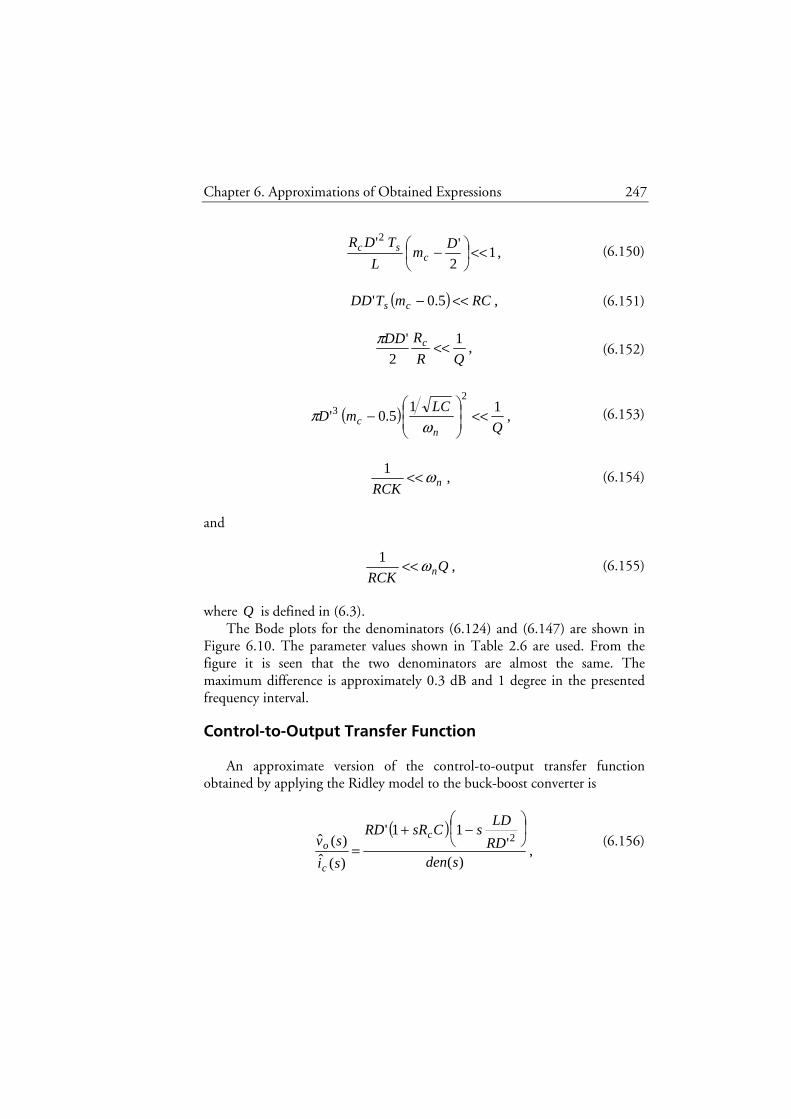
Chapter 6. Approximations of Obtained Expressions 247
,12
''2<<
− D
mL
TDRc
sc (6.150)
( ) ,5.0' RCmTDD cs <<− (6.151)
,1
2
'
QR
RDD c <<π (6.152)
( ) ,11
5.0'
23
Q
LCmD
nc <<
−
ωπ (6.153)
,1
nRCKω<< (6.154)
and
,1
QRCK nω<< (6.155)
where Q is defined in (6.3).
The Bode plots for the denominators (6.124) and (6.147) are shown in Figure 6.10. The parameter values shown in Table 2.6 are used. From the figure it is seen that the two denominators are almost the same. The maximum difference is approximately 0.3 dB and 1 degree in the presented frequency interval.
Control-to-Output Transfer Function
An approximate version of the control-to-output transfer function obtained by applying the Ridley model to the buck-boost converter is
( )
,)(
'11'
)(ˆ)(ˆ 2
sdenRD
LDsCsRRD
si
sv c
c
o
−+=
(6.156)
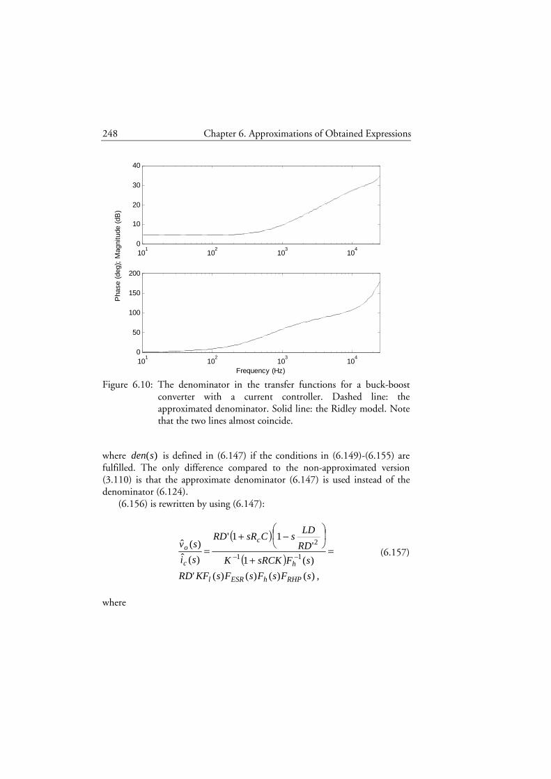
248 Chapter 6. Approximations of Obtained Expressions
Figure 6.10: The denominator in the transfer functions for a buck-boost converter with a current controller. Dashed line: the approximated denominator. Solid line: the Ridley model. Note that the two lines almost coincide.
where )(sden is defined in (6.147) if the conditions in (6.149)-(6.155) are fulfilled. The only difference compared to the non-approximated version (3.110) is that the approximate denominator (6.147) is used instead of the denominator (6.124).
(6.156) is rewritten by using (6.147):
( )
( ),)()()()('
)(1
'11'
)(ˆ)(ˆ
11
2
sFsFsFsKFRD
sFsRCKK
RD
LDsCsRRD
si
sv
RHPhESRl
h
c
c
o =+
−+
= −− (6.157)
where
101
102
103
104
0
10
20
30
40
101
102
103
104
0
50
100
150
200
Frequency (Hz)
Pha
se (
deg)
; M
agni
tude
(dB
)
Chapter 6. Approximations of Obtained Expressions 249
,1
1)(
sRCKsFl +
= (6.158)
,'
1)(2RD
LDssFRHP −= (6.159)
)(sFESR is defined in (6.42), )(sFh is defined in (6.2), and K is defined in
(6.148).
Output Impedance
The output impedance obtained by applying the Ridley model to the buck-boost converter is given by (3.111). The numerator in (3.111) will first be approximated. By using (6.149) and the fact that D and 'D are positive numbers less than or equal to unity, the following is obtained:
.'''' RRDRDRDDRR
RDDR ccc
cc ≤<<≤≤<< (6.160)
The numerator in (3.111) is approximated by using (6.160):
( )
.''
'
1)(
2
22
2
22
+++++
−
•+=
DmsTs
Q
s
RD
R
L
RDDmT
R
DRR
CsRRsnum
csnzn
cccsc
c
ωω (6.161)
One part of (6.161) is approximated by using (2.39) and (6.160):
( )
( ) .''
1
'1'
'
''
'
'
2
2
2
2
22
DmmL
TDR
DmL
TDR
RD
RR
RDDRRD
RD
R
L
RDDmT
R
DRR
ccsc
csc
cc
c
cccsc
−+
≈−++−
=++−
(6.162)

250 Chapter 6. Approximations of Obtained Expressions
The second term in (6.162) is approximated by using (6.150) and the fact that cm is a positive number greater than or equal to unity:
( ) .1'2
1''
' 22
<<
−≤− Dm
L
TDRDmm
L
TDRc
sccc
sc (6.163)
Hence, (6.162) is approximately equal to unity. The numerator (6.161) can therefore by approximated with:
( ) )(1)( 1 sFCsRRsnum hc−+≈ (6.164)
according to (3.54).
An approximate version of the output impedance obtained by applying the Ridley model to the buck-boost converter is
( )
,)(
)(1)(
1
sden
sFCsRRsZ hc
out
−+= (6.165)
where )(sden is defined in (6.147) and )(sFh is defined in (6.2) if the conditions in (6.149)-(6.155) are fulfilled. The only differences compared to the non-approximated version (3.111) are that the approximate denominator (6.147) is used instead of the denominator (6.124) and that the approximate numerator (6.164) is used instead of the numerator in (3.111).
(6.165) is rewritten by using (6.147):
( )( )
,)()()(1
)(1)(
11
1
sFsRKFsFsRCKK
sFCsRRsZ ESRl
h
hcout =
++
= −−
− (6.166)
where K is defined in (6.148), )(sFl is defined in (6.158), and )(sFESR is defined in (6.42). The two high-frequency poles are cancelled by two of the zeros.
Audio Susceptibility
The expression for the audio susceptibility obtained by applying the Ridley model to the buck-boost converter was improved in Chapter 5 by
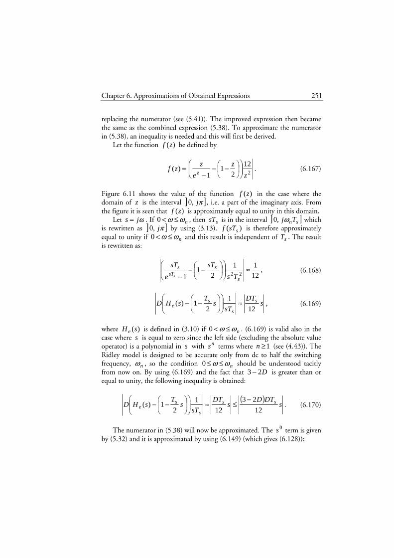
Chapter 6. Approximations of Obtained Expressions 251
replacing the numerator (see (5.41)). The improved expression then became the same as the combined expression (5.38). To approximate the numerator in (5.38), an inequality is needed and this will first be derived.
Let the function )(zf be defined by
.12
21
1)(
2z
z
e
zzf
z
−−
−= (6.167)
Figure 6.11 shows the value of the function )(zf in the case where the domain of z is the interval ] ]πj,0 , i.e. a part of the imaginary axis. From the figure it is seen that )(zf is approximately equal to unity in this domain.
Let ωjs = . If nωω ≤<0 , then ssT is in the interval ] ]snTjω,0 which is rewritten as ] ]πj,0 by using (3.13). )( ssTf is therefore approximately equal to unity if nωω ≤<0 and this result is independent of sT . The result is rewritten as:
,12
11
21
1 22≈
−−− s
ssT
s
Ts
sT
e
sTs
(6.168)
,12
1
21)( s
DT
sTs
TsHD s
s
se ≈
−− (6.169)
where )(sH e is defined in (3.10) if nωω ≤<0 . (6.169) is valid also in the case where s is equal to zero since the left side (excluding the absolute value operator) is a polynomial in s with ns terms where 1≥n (see (4.43)). The Ridley model is designed to be accurate only from dc to half the switching frequency, nω , so the condition nωω ≤≤0 should be understood tacitly from now on. By using (6.169) and the fact that D23 − is greater than or equal to unity, the following inequality is obtained:
( )
.12
23
12
1
21)( s
DTDs
DT
sTs
TsHD ss
s
se
−≤≈
−− (6.170)
The numerator in (5.38) will now be approximated. The 0s term is given
by (5.32) and it is approximated by using (6.149) (which gives (6.128)):

252 Chapter 6. Approximations of Obtained Expressions
Figure 6.11: The value of the function )(zf (see (6.167)) in the case where the domain of z is the interval ] ]πj,0 , i.e. a part of the imaginary axis.
.'2
1''
'21
''
D
DDDmD
L
RT
D
DD
RR
RRDmD
L
RT
cs
c
cc
s
+
−−
≈+
−−
++
(6.171)
The other terms are given by (5.34) and they are approximated by using (6.149) (which gives (6.128)):
0 0.5 1 1.5 2 2.5 30
0.5
1
1.5
Im(z)
f(z)

Chapter 6. Approximations of Obtained Expressions 253
( )
( )
( ) ( )
( ) ( )
( ) ,1)('
1
21)(
'
21
24
21
12
23
21
'
1)(''
'
1
21)(
'
'1
21)(
'
''
2
222
2
1
−+
−−
+
−−+
+−−
−−−−
•
≈−++
+
−−
++
−
+
−−
++
−
sFD
D
sTs
TsHD
RD
R
Ds
DTDDs
DTDD
DL
RT
sFD
D
RRD
RRD
sTs
TsH
RRD
RRD
DsF
RRD
RRDD
L
RT
fs
se
c
ss
s
fc
c
s
se
c
c
fc
cs
K
(6.172)
where )(1 sF f is defined in (4.60), )(2 sF f is defined in (4.61), and )(sHe is defined in (3.10). (6.172) is approximated by using (6.149) and (6.170) and the result is:
( ).1)('2
1)(' 21 −+
−−− sF
D
DDsFD
L
RTff
s (6.173)
An approximate version of the numerator in (5.38) is obtained by adding (6.171) and (6.173):
( )
( ) .)('
)(''
1)(''
21)(
21''
21
2
1
sFD
DsFDmD
L
RT
sFD
D
D
D
DsF
DDmD
L
RT
ffcs
f
fcs
+−
=−+
+
−−−
−−
(6.174)

254 Chapter 6. Approximations of Obtained Expressions
The expression for the audio susceptibility obtained by applying the Ridley model to the buck-boost converter was improved in Chapter 5. An approximate version of the improved expression is
( ) ( )
,)(
1)('
)(''
)(ˆ
)(ˆ 21
sden
CsRDsFD
DsFDmD
L
RT
sv
sv cffcs
g
o
+
+−
=(6.175)
where
( ) ( )
,24
21
12
23
21
1
1
1
1)(
222
1
K++−
−−
−
−
=
−−−
−=
−
−
sDTDD
sDTDD
e
sT
sDT
e
e
sT
sTsF
ss
sTs
s
sDT
sTs
sf
s
s
s
(6.176)
( ),
12
231
2
'1
1
11)( 2
22
2 K++−
++=−
−= −
−s
TDDs
TD
e
e
DsF ss
sT
sDT
fs
s
(6.177)
(see (4.60) and (4.61)), and )(sden is defined in (6.147) if the conditions in (6.149)-(6.155) are fulfilled. The only differences compared to the non-approximated improved version (5.38) are that the approximate )(sden in (6.147) is used instead of )(sden in (6.124) and that the numerator in (5.38) is replaced by its approximate version (6.174).
(6.175) is rewritten by using (6.147):
( ) ( )
( )
( ) ,)()()()('
)(''
)(1
1)('
)(''
)(ˆ
)(ˆ
21
11
21
sFsFsDKFsFD
DsFDm
L
DRT
sFsRCKK
CsRDsFD
DsFDmD
L
RT
sv
sv
hESRlffcs
h
cffcs
g
o
+−
=+
+
+−
=−− (6.178)
where )(1 sF f is defined in (6.176), )(2 sF f is defined in (6.177), K is defined in (6.148), )(sFl is defined in (6.158), )(sFESR is defined in (6.42), and )(sFh is defined in (6.2).
Chapter 6. Approximations of Obtained Expressions 255
)(sk f defined in (5.44) will now be approximated. The 0s term of the numerator of )(sk f is written as
( )( )
( )( ) ( )
( ) ( )( )( )
( ) ( ) ( )( )( )
( )( ) .
21
21
'
'
'
'
'
11
'
'
'
21
'
1
'
'
'1
'
'
'
'
'
21
'21
'
'
2
2
2
2
−−=
−
++
++
−
=
+
−+−−+−++
−
−
+++−
++
−
=
+
−−++
++
−
−
++
−
++
−
D
L
RDTD
RRD
RRD
RRD
RRD
L
RDT
RRD
DRRRDRDR
RRD
RRD
RD
RD
D
RRD
DRRRD
RRD
RRD
L
RDT
RRD
DR
RRD
RRD
RRD
RRD
RD
RD
D
RRD
DRD
RRD
RRD
L
RDT
is
c
c
c
cis
c
ccc
c
ci
c
cc
c
cis
c
c
c
c
c
ci
c
c
c
cis
(6.179)
The other terms of the numerator of )(sk f are approximated by using (6.149) (which gives (6.128)):

256 Chapter 6. Approximations of Obtained Expressions
( )
( )
( )( ) ( )
( ) ( )
( ) ,1)('
1
21)(
'
21
24
21
12
23
21
1)('
'
'
'
'
1
21)(
'
'1
21)(
'
'
22
2
2
2
222
22
2
2
2
1
−−
+
−
−−
−
−−+
+−−
−−−
•−
≈
−−
+
++
++
−
−−
++
−
−
−−
++
−
sFs
Q
s
RD
RD
sTs
TsHD
RD
R
Ds
DTDDs
DTDD
L
RDT
sFs
Q
s
RRD
RRD
RRD
RRD
RD
RD
sTs
TsH
RRD
RRD
DsF
RRD
RRD
L
RDT
fnzn
i
s
se
c
ss
is
fnznc
c
c
ci
s
se
c
c
fc
cis
ωω
ωω
K
(6.180)
where )(1 sF f is defined in (6.176), )(2 sF f is defined in (6.177), and
)(sHe is defined in (3.10). (6.180) is approximated by using (6.149) and (6.170) and the result is:
( ) ,)()('2
1)( 22
2
1 sFsHRD
RDDsF
L
RDTfe
if
is −−
−−− (6.181)
where )(sHe is defined in (3.14). An approximate version of )(sk f is obtained by replacing the numerator in (5.44) with the sum of (6.179) and (6.181) and the result is:
( ) ,'
1)()('
)()(1
222
2
1
−
−
−−−=
RD
LDssFsH
RD
RDsF
L
RDTsk fe
if
isf
(6.182)
where )(1 sF f is defined in (6.176), )(2 sF f is defined in (6.177), and )(sHe is defined in (3.14). A second step to approximate )(sk f is to
approximate )(sF f and )(2 sF f .
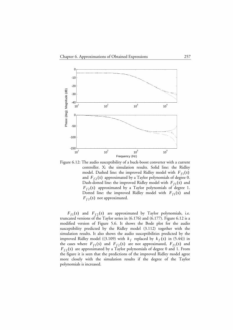
Chapter 6. Approximations of Obtained Expressions 257
Figure 6.12: The audio susceptibility of a buck-boost converter with a current controller. X: the simulation results. Solid line: the Ridley model. Dashed line: the improved Ridley model with )(1 sF f and )(2 sF f approximated by a Taylor polynomials of degree 0. Dash-dotted line: the improved Ridley model with )(1 sF f and
)(2 sF f approximated by a Taylor polynomials of degree 1. Dotted line: the improved Ridley model with )(1 sF f and
)(2 sF f not approximated.
)(1 sF f and )(2 sF f are approximated by Taylor polynomials, i.e. truncated versions of the Taylor series in (6.176) and (6.177). Figure 6.12 is a modified version of Figure 5.6. It shows the Bode plot for the audio susceptibility predicted by the Ridley model (3.112) together with the simulation results. It also shows the audio susceptibilities predicted by the improved Ridley model ((3.109) with fk replaced by )(sk f in (5.44)) in the cases where )(1 sF f and )(2 sF f are not approximated, )(1 sF f and
)(2 sF f are approximated by a Taylor polynomials of degree 0 and 1. From the figure it is seen that the predictions of the improved Ridley model agree more closely with the simulation results if the degree of the Taylor polynomials is increased.
101
102
103
104
-40
-30
-20
-10
0
101
102
103
104
-150
-100
-50
0
Frequency (Hz)
Pha
se (
deg)
; M
agni
tude
(dB
)

258 Chapter 6. Approximations of Obtained Expressions
6.5 Summary and Concluding Remarks
In this chapter, the expressions obtained from the (improved) Ridley model were approximated. To derive these approximations, we assumed that the distance from the origin to the low-frequency pole is much smaller than the distance from the origin to the two high-frequency poles. We also made some other assumptions to obtain simple expressions.
Since the denominators for the control-to-output transfer function, output impedance, and audio susceptibility are the same (for each specific converter), we approximated the common denominator only once (for each specific converter). The most complicated numerators were simplified the most. Therefore, the approximated numerators are approximately equally simple. The expressions for the audio susceptibility depend on )(sF f ( )(1 sF f and )(2 sF f ). The expressions for )(sF f were therefore also approximated.
259
Chapter 7 Using Load Current for Control
The output voltage and the inductor current are measured in the case where current-mode control is utilized. In this chapter, some properties that can be obtained when the controller also utilizes load current measurements are analyzed. The results of this analysis are compared with simulation results.
The analysis in this chapter is partly based on the approximate expressions obtained in Chapter 6. This may result in unreliable analysis (see Section 7.7).
7.1 Chapter Survey
Some of the previous works made in this area are reviewed in Section 7.2. In Section 7.3, a simple model of the buck converter with current-mode control is used to give a simple explanation of some of the properties that are obtained when using load current measurements to control the converter. In Section 7.4, the model obtained in Chapter 6 for the buck converter with current-mode control is used to analyze the properties and the results are compared with simulation results. The same is made for the boost and buck-boost converters in Section 7.5 and Section 7.6, respectively. A summary and concluding remarks are presented in Section 7.7.
7.2 A Review
A number of papers suggest that the load current should be measured in order to improve the control of dc-dc converters. A few of them are mentioned in this section.
Redl and Sokal (1986) show that the transient in the output voltage due

260 Chapter 7. Using Load Current for Control
Figure 7.1: The configuration of the controller.
to a step change in the load can be much reduced if the load current is measured and used to control the converter. They only consider the case where current-mode control is used. The configuration of the controller is shown in Figure 7.1. The inductor current, )(tiL , is fed back in the inner loop. The inner loop consists of the current controller and the converter. The load current, )(tiload , is used in the middle loop. (The input voltage, )(tvg , and output voltage, )(tvo , are in some cases also used in the middle loop.) The middle loop consists of a controller and a process where the process is the closed inner loop. The output voltage, )(tvo , is fed back in the outer loop. The outer loop consists of a voltage controller and a process where the process is the closed middle loop. The control method includes an extra middle controller compared to current-mode control (compare Figure 7.1 and Figure 3.1). The control signal of the voltage controller is now called )(2 tic and it affects the middle controller. The reference signal for the current controller is still called )(tic . The middle controller should be as follows according to Redl and Sokal (1986).
Buck: ,)()()( 2 tititi loadcc += (7.1)
Boost: ,)()(
)()()( 2 ti
tv
tvtiti load
g
occ += (7.2)
Buck-boost: .)()(
)()()()( 2 ti
tv
tvtvtiti load
g
gocc
++= (7.3)
ic2(t) Controller using load
current
Currentcontroller
iload(t) ic(t) δ (t)
iL(t)
Converter
vo(t) vg(t)
vref(t) Voltagecontroller
Chapter 7. Using Load Current for Control 261
The numerator in (7.3), )()( tvtv go + , is actually not what is proposed by Redl and Sokal (1986). Instead, )()( tvtv go − is used but in Kislovski, Redl and Sokal (1991, Section 11.2) )()( tvtv go + is used. If )()( tvtv go − is used as the numerator in (7.3), then (7.3) does not make sense with the definitions of signs of voltages and currents made in this thesis.
Schoneman and Mitchell (1989) analyze the proposed use of load current further in the case of a buck converter, i.e. (7.1).
Redl and Sokal (1986) suggest that the load current is not measured directly but calculated indirectly. For example, in a buck converter, the inductor current, )(tiL , and the current to the output capacitor, )(ticap , are measured. The load current can then be calculated as the difference (see Figure 2.1):
.)()()( tititi capLload −= (7.4)
Note that the inductor current is measured in current-mode control so it is still only necessary to measure one extra current compared to current-mode control.
Schoneman and Mitchell (1989) propose an alternative approach. From Figure 3.4, it is seen that the difference )()( titi Lc − is calculated in the current controller. This difference is rewritten by using (7.1) and (7.4):
.)()()()()()(
)()()()()(
22
2
titititititi
tititititi
capcLcapLc
LloadcLc
−=−−+=−+=−
(7.5)
Hence, it is not necessary to measure the inductor and load currents. Only the current to the output capacitor must be measured.
Hiti and Borojevic (1993) use the measured load current to modify the current-mode control for the boost converter. The modification is made in such a way that the dc gain of the closed middle loop in Figure 7.1 (i.e. the transfer function that describes how )(tvo is affected by )(2 tic ) is independent of the load. The modification turns out to be the same as the one presented for the boost converter by Redl and Sokal (1986), i.e. (7.2).

262 Chapter 7. Using Load Current for Control
Figure 7.2: The basic configuration of the controller.
7.3 Principal Properties
In this section, some properties obtained by using measured load current are explained by using a simple model of the buck converter with current-mode control. The properties are:
• Low output impedance. • An almost invariant control-to-output transfer function for different
loads. • Risk of instability.
However, two concepts in control theory, feedforward and gain scheduling, are first reviewed.
Feedforward and Gain Scheduling
Figure 7.2 shows the configuration of the controller used as a base here. The control signal of the controller is called u and it controls the input signal of the process that should be controlled. The output signal of the process is called y and it is fed back to the controller. The reference signal of the controller is called r . The controller is very general since the compensators
1C and 2C can be chosen independently. The definition of feedforward is that a disturbance signal is measured and
used to make a change in the control signal before the disturbance has caused
r u y C1
C2
Process
Controller

Chapter 7. Using Load Current for Control 263
Figure 7.3: A controller with feedforward.
any change in the output of the process (Åström and Hägglund, 1995, Section 7.3). Figure 7.3 shows an example where the controller in Figure 7.2 is extended to also include feedforward. The disturbance signal is called v and it is multiplied with ffC to obtain the contribution to the control signal from the feedforward part. Feedforward does not cause any stability problems (Åström and Hägglund, 1995, Section 7.3). A consequence of this is that, for linear systems, feedforward does not affect the loop gain.
Before continuing with gain scheduling, some more examples of feedforward will be considered. One input signal to the middle controller in Figure 7.1 is (in some cases) the input voltage, )(tvg , and it is a disturbance signal. If Figure 7.1 is compared with Figure 7.3, it is clear that the use of the measured input voltage in the controller should be called feedforward. Another input signal to the middle controller is the load current, )(tiload . Whether the use of the measured load current should be called feedforward or not will be analyzed later in this section. Yet another input signal to the middle controller is (in some cases) the output voltage, )(tvo . The output voltage depends on the state variables in the controller and it should therefore not be regarded as a disturbance signal. The use of the measured output voltage should therefore not be called feedforward. Ridley (1990a) uses the expression “feedforward gains fk and rk ”. From Figure 3.8 and the previous discussion, it is concluded that it is correct to use the expression “feedforward gain fk ” but not the expression “feedforward gain rk ”. Both of these expressions are used in this thesis even though it is not formally correct.
r u y
C1
C2
Process
Controller withfeedforward v
Cff
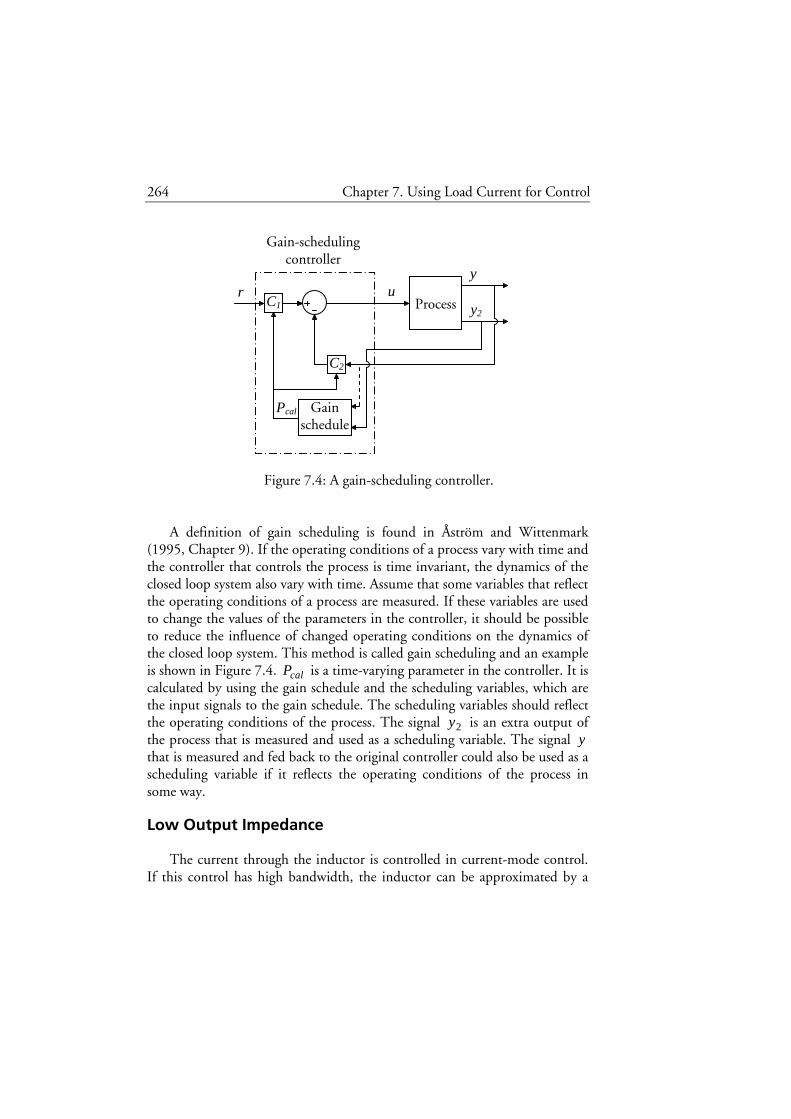
264 Chapter 7. Using Load Current for Control
Figure 7.4: A gain-scheduling controller.
A definition of gain scheduling is found in Åström and Wittenmark
(1995, Chapter 9). If the operating conditions of a process vary with time and the controller that controls the process is time invariant, the dynamics of the closed loop system also vary with time. Assume that some variables that reflect the operating conditions of a process are measured. If these variables are used to change the values of the parameters in the controller, it should be possible to reduce the influence of changed operating conditions on the dynamics of the closed loop system. This method is called gain scheduling and an example is shown in Figure 7.4. calP is a time-varying parameter in the controller. It is calculated by using the gain schedule and the scheduling variables, which are the input signals to the gain schedule. The scheduling variables should reflect the operating conditions of the process. The signal 2y is an extra output of the process that is measured and used as a scheduling variable. The signal y that is measured and fed back to the original controller could also be used as a scheduling variable if it reflects the operating conditions of the process in some way.
Low Output Impedance
The current through the inductor is controlled in current-mode control. If this control has high bandwidth, the inductor can be approximated by a
r y2
u y
C1
Gain schedule
Pcal
C2
Process
Gain-schedulingcontroller

Chapter 7. Using Load Current for Control 265
Figure 7.5: A simple model of the buck converter with current-mode control.
Figure 7.6: The measured load current affects the control signal.
controlled current source. The buck converter with current-mode control can then be modeled as in Figure 7.5 (compare with Figure 1.2). The current from the current source is equal to the reference signal for the current controller, )(tic . The ESR of the capacitor is neglected in Figure 7.5.
Figure 7.6 shows how the measured load current should be used to control the buck converter according to (7.1). If )(tiload changes, )(tic changes by the same amount, provided that )(2 tic is constant, e.g. when the voltage controller is disabled. Consequently, the capacitor current does not change. The conclusion is that changes in load current do not affect the output voltage, that is, the output impedance is zero:
.0)(
)()( =−=
si
svsZ
load
oout (7.6)
Load
vo(t) C
iload(t)
Voltage controller
Vref ic(t) ic(t)
Load
vo(t) C ic2(t)
iload(t)
Voltage controller
Vref ic(t) ic(t)
iload(t)

266 Chapter 7. Using Load Current for Control
The output impedance is zero also in the case where the voltage controller is enabled since a load change does not cause a change in the output voltage according to (7.6). Note that the definition of output impedance used in (7.6) is not the same as the one used elsewhere in this thesis, e.g. (2.91). According to Erickson and Maksimovic (2000, preamble of Chapter 8), the load resistance, R , can either be included in the output impedance as in (2.91) (see Figure 2.6) or excluded as in (7.6).
An Almost Invariant Control-to-Output Transfer Function for Different Loads
In this subsection, the control-to-output transfer function that describes how )(2 tic affects )(tvo is analyzed. Two different types of loads are considered. The first type is a current source, i.e. the load current is independent of the output voltage. The second type is a linear resistive load.
First assume that the load is a current source. If the load current is not used, )(tic is equal to )(2 tic and the output voltage is
( ) .)()(1
)( 2 sisisC
sv loadco −= (7.7)
Since )(tiload is determined by the current source, it can be regarded as an input signal in addition to )(2 tic . The control-to-output transfer function that describes how )(2 tic affects )(tvo is therefore obtained if )(tiload is set to zero:
.1
)(
)()(
0)(22 sCsi
svsG
sic
oiv
load
co==
=
(7.8)
If the load current is used, )(tic is according to (7.1) and the output voltage is
( )
( ) )(1
)()()(1
)()(1
)(
22 sisC
sisisisC
sisisC
sv
cloadloadc
loadco
=−+
=−=(7.9)

Chapter 7. Using Load Current for Control 267
and )(2
sGcoiv is
.1
)(
)()(
22 sCsi
svsG
c
oiv co
== (7.10)
It is seen from (7.8) and (7.10) that the control-to-output transfer function
)(2
sGcoiv does not change when the measured load current is introduced for
control. Therefore, the loop gain and the stability properties do not change. Since the load current does not depend on the states of the converter, it can be seen as a disturbance signal. The conclusion is that the use of measured load current for control is feedforward in the case where the load is a current source.
Now assume that the load is a resistor with resistance R . If the load current is not used, )(
2sG
coiv is
.1
1
)(
)()(
22
sCR
sCR
si
svsG
c
oiv co
+== (7.11)
If the load current is used, the output voltage is given by (7.9) and )(
2sG
coiv is given by (7.10). It is seen from (7.11) and (7.10) that )(
2sG
coiv changes from the impedance of the parallel of the capacitor and resistor to just the impedance of the capacitor when the measured load current is introduced for control. Since R is not present in (7.10), the use of the load current makes the control-to-output transfer function )(
2sG
coiv invariant for different values of R , i.e. different linear resistive loads.
If the load is a resistor and the measured load current is introduced for control, the control-to-output transfer function )(
2sG
coiv changes, as shown above, and can also become unstable, as will be shown in the next subsection. The conclusion is that the use of measured load current for control is not feedforward in the case where the load is a resistor. It can instead be seen as gain scheduling, as now will be shown. Figure 7.7 is a modified version of Figure 7.1. The closed inner loop in Figure 7.1 is regarded as the process to be controlled in Figure 7.7. The controller in Figure 7.7 controls the input signal of the process, )(tic . The output signals of the process, )(tvo and
)(tiload , are measured and used by the controller. The controller consists of

268 Chapter 7. Using Load Current for Control
Figure 7.7: A configuration of the controller where the gain-scheduling
property is emphasized.
two voltage controllers in cascade: an outer voltage controller and a gain-scheduling voltage controller. The outer voltage controller then controls a “process” which is the closed loop of the gain-scheduling voltage controller and the process. Assume that the gain-scheduling voltage controller is designed just to make this “process” invariant for different linear resistive loads. Assume further that the outer voltage controller is designed thereafter to obtain the wanted properties of the whole closed loop system. If the designed gain-scheduling voltage controller is
,1)(1 =tC (7.12)
,)(
1)(2 tR
tCcal
−= (7.13)
ic2 (Outer) voltage
controller
Currentcontroller
iload ic δ
iL
vo
Vref C1
Gain schedule
Rcal
C2
Converter
Process Controller
Gain-schedulingvoltage controller

Chapter 7. Using Load Current for Control 269
,)(
)()(
ti
tvtR
load
ocal = (7.14)
then the control signal is
.)()()(
)(
)(1
)(
)()(
1)()()()()()(
22
2221
tititv
ti
tvti
tvtR
titvtCtitCti
loadco
load
oc
ocal
cocc
+=+
=+=−=
(7.15)
Hence, the gain-scheduling voltage controller is exactly the same as the middle controller in Figure 7.1 for the buck converter, i.e. (7.1). The use of measured load current for control can therefore be seen as gain scheduling.
It was shown previously that the control-to-output transfer function )(
2sG
coiv is invariant for different linear resistive loads if (7.1) is used. The designed gain-scheduling voltage controller, (7.12)-(7.14), is therefore reasonable since it is equivalent to (7.1) and the purpose was to obtain invariance for different linear resistive loads. The gain-scheduling voltage controller can be designed by using model matching, but this will be shown first in the next section.
The simple model in Figure 7.5 gives the following description of the process in Figure 7.7 in the case where the load is a resistor:
,1
1
)(
)()(
sCR
sCR
si
svsG
c
oiv co
+== (7.16)
.)(
)(R
svsi o
load = (7.17)
This is a first order system and the most natural choice for the state variable is the voltage across the capacitor, which is the same as the output voltage,
)(tvo . )(tvo and )(tiload are both measurements of this state, where the latter one is scaled by the factor R1 . If the controller knows the value of R ,
270 Chapter 7. Using Load Current for Control
it will control the process equally well with only )(tiload measured compared to if only )(tvo is measured.
That both signals are measured and used by the controller is in the above gain-scheduling approach interpreted as follows. )(tvo is a measurement of the state and is fed back to the controller. The controller shall try to control the process such that )(tvo is equal to reference signal refV and it is therefore a voltage controller. The value of the load resistance, R , will be a parameter in the voltage controller. The operating conditions of the process vary with time since the load resistance varies. To reduce the influence of the changed dynamics of the process, the parameter R in the controller is replaced by the time-varying parameter )(tRcal . It should be an estimate of the load resistance. To be able to calculate this estimate, an extra variable that reflects the operating conditions of a process must be measured and it is the load current, )(tiload . An estimate of the load resistance can now be calculated with the gain schedule (7.14). )(tiload and also )(tvo are used as scheduling variables. The calculated estimate, )(tRcal , is equal to the load resistance, R , if there are no measurement errors.
An alternative interpretation of that )(tvo and )(tiload are both measured, is that it is the output power, )()( titv loado , that is measured and used to control the input power (Hiti and Borojevic, 1993).
Schoneman and Mitchell (1989) use a load consisting of both a resistor and a current source. The load current is in this case dependent of the output voltage. The authors say that the load current is fed forward, but this is thus not correct, strictly speaking. They also claim that the “feedforward” does not affect the loop gain. The reason for this erroneous conclusion is that the authors at a point in the derivation neglect the changes of the current through the resistor.
Risk of Instability
From Figure 7.6, it is seen that there is positive feedback in the load current loop. This indicates that there can be a problem with the stability in the case where the load is a resistor. To investigate the stability, Figure 7.6 is generalized to obtain Figure 7.8, where the gain in the measurement of the load current is iH . In a real system, iH is not exactly equal to 1, but the measurement can be made such that iH is close to 1. The output voltage is

Chapter 7. Using Load Current for Control 271
Figure 7.8: A measurement gain, iH , is introduced for the load current.
( ) .)()(
)(1
)()(1
)( 2
−+=−=R
sv
R
svHsi
sCsisi
sCsv oo
icloadco (7.18)
Hence, the control-to-output transfer function )(
2sG
coiv is
( ) ( )
.1
1
1
11
1
1
)(
)()(
22
−+
=−−
==
RCHsCH
sRC
sCsi
svsG
iic
oiv co
(7.19)
)(
2sG
coiv has a pole at
( ) .1
11 RCHp i−−= (7.20)
If iH >1, the system is unstable since the pole is in the right half side in the complex s-plane. If iH =1, the system has a pole in the origin and the system acts as an integrator. If iH <1, the system is stable and the dc gain is
( )iHR −1 , i.e. very high if iH is close to 1. The conclusion of all this is that it is difficult or impossible to obtain a specific output voltage by manually setting a value for )(2 tic if iH is close to 1. Instead, an outer voltage controller is used to set )(2 tic and the system can be stabilized.
vo(t) C ic2(t)
R
iload(t)
Voltage controller
Vref
Hi
ic(t) ic(t)
iload(t)

272 Chapter 7. Using Load Current for Control
Summary
Analysis was made in this section by using a simple model of the buck converter with current-mode control. We concluded the following.
1. The output impedance can become zero if the measured load current is
used for control. 2. The following properties are obtained in the case where the load is a
current source: • The use of measured load current for control is feedforward. • The control-to-output transfer function does not change when this
feedforward is introduced. 3. The following properties are obtained in the case where the load is a
linear resistor: • The control-to-output transfer function can change when the
measured load current is introduced for control. • The converter can become unstable when the measured load current
is introduced for control. • The control-to-output transfer function can be invariant for different
linear resistive loads if the measured load current is used for control. • The use of measured load current for control is not feedforward. It
can instead be seen as gain scheduling. Some properties that can be obtained in the case where the load is a linear
resistor and the controller uses load current measurements will be analysed further in the next sections by using the models obtained in Chapter 6.
7.4 Properties of the Buck Converter
In Section 6.2, approximate expressions for the buck converter with current-mode control were derived. In this section, these expressions are used to analyze how the control-to-output transfer function, the output impedance and the audio susceptibility are affected when using load current measurements to control the converter. An expression for the output voltage is first derived and this is then used to derive the three transfer functions. The results are compared with simulation results and the used simulation models are presented at the end of this section. In this section, it is assumed that the
Chapter 7. Using Load Current for Control 273
conditions in (6.34)-(6.38) are fulfilled since the approximate expressions derived in Section 6.2 may not be valid otherwise.
An Expression for the Output Voltage
To make the analysis in this section general, a transfer function, )(sHi , is introduced in (7.1):
.)(ˆ)()(ˆ)(ˆ
2 sisHsisi loadicc += (7.21)
)(sHi can represent the dynamics of a filter, which filters the signal from the load-current sensor, and also the sensor itself. From Figure 2.6, it is seen that the load current is
.)()(
)( tiR
tvti inj
oload += (7.22)
Figure 7.9 shows the system obtained by using (7.21) and (7.22). In Chapter 3, the subscript ol was introduced to denote the converter transfer functions, i.e. the open loop system. This system is controlled by changing the duty cycle, )(tδ . If the inductor current is fed back, a new system is obtained which is controlled by changing )(tic . The transfer functions for this new system will be denoted with the subscript 2ol . However, it is not used for the control-to-output transfer function since there is no risk of confusion in that case. Since linear models are used, the output voltage is obtained by adding the contribution from each input signal.
The following is obtained from Figure 7.9:
.)(ˆ)(ˆ
)(ˆ)(ˆ
)(ˆ)(ˆ
)(ˆ)(ˆ)()(ˆ
)(ˆ)(ˆ
)(ˆ)(ˆ
)(ˆ)(ˆ
)(ˆ)(ˆ
)(ˆ)(ˆ)(ˆ
)(ˆ
22
2
22
svsv
svsi
si
sv
siR
svsHsi
si
sv
svsv
svsi
si
svsi
si
svsv
g
olg
oinj
olinj
o
injo
icc
o
g
olg
oinj
olinj
oc
c
oo
+
+
++
=
+
+=
(7.23)
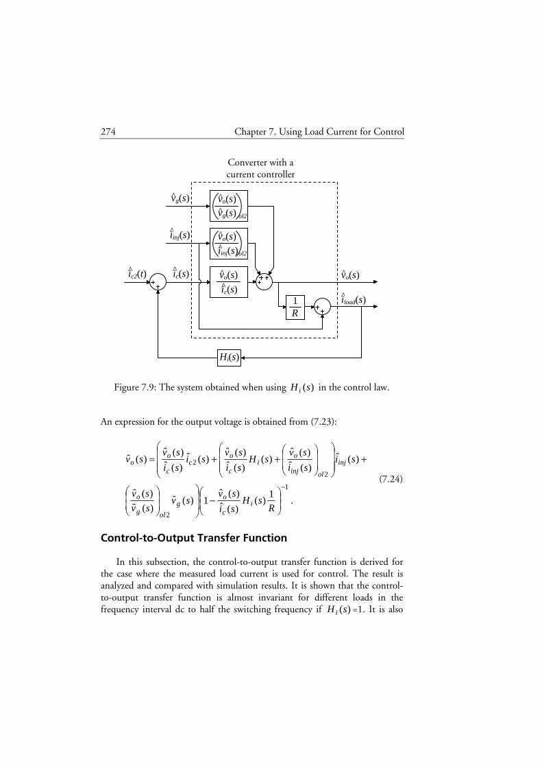
274 Chapter 7. Using Load Current for Control
Figure 7.9: The system obtained when using )(sHi in the control law.
An expression for the output voltage is obtained from (7.23):
.1
)()(ˆ)(ˆ
1)(ˆ)(ˆ
)(ˆ
)(ˆ)(ˆ)(ˆ
)()(ˆ)(ˆ
)(ˆ)(ˆ)(ˆ
)(ˆ
1
2
2
2
−
−
+
++=
RsH
si
svsv
sv
sv
sisi
svsH
si
svsi
si
svsv
ic
og
olg
o
inj
olinj
oi
c
oc
c
oo
(7.24)
Control-to-Output Transfer Function
In this subsection, the control-to-output transfer function is derived for the case where the measured load current is used for control. The result is analyzed and compared with simulation results. It is shown that the control-to-output transfer function is almost invariant for different loads in the frequency interval dc to half the switching frequency if )(sHi =1. It is also
iload(s)
ic2(t) ic(s)
Converter with acurrent controller
vo(s)
iinj(s)
iinj(s) ^
vo(s) ^
ol2
ic(s) ^
vo(s) ^
vg(s) ^
vo(s) ^
ol2
1 R
vg(s)
Hi(s)
^
^
^ ^
^
^

Chapter 7. Using Load Current for Control 275
shown that invariance (theoretically) is obtained for a specific )(sHi . Furthermore, it is shown that this specific )(sHi can be obtained by designing a gain-scheduling controller.
The approximate control-to-output transfer function (6.40) is repeated here for convenience:
,)()()()(ˆ)(ˆ
)( sFsFsRKFsi
svsG hESRl
c
oiv co
== (7.25)
where
( ),
5.0'1
1
−+=
DmL
RTK
cs
(7.26)
,1
1)(
sRCKsFl +
= (7.27)
,1)( CsRsF cESR += (7.28)
,
1
1)(
2
2
nn
hs
Q
ssF
ωω++
= (7.29)
nω is defined in (3.13), Q is defined in (3.20), and cm is defined in (3.21). To obtain the control-to-output transfer function of the closed loop
system where (7.21) is used, the two input signals )(ˆ svg and )(ˆ siinj are set to zero in (7.24):
.1
)()(ˆ)(ˆ
1
)(ˆ)(ˆ
)(ˆ)(ˆ
2
RsH
si
svsi
sv
si
sv
ic
o
c
o
c
o
−= (7.30)
(7.30) is rewritten by using (7.25):
276 Chapter 7. Using Load Current for Control
.)()()()(
)()(
)()()()(1
)()()(
)(ˆ)(ˆ
)(
1111
22
sHsFsFRsFKR
sFsF
sHsFsFsKF
sFsFsRKF
si
svsG
ihESRl
hESR
ihESRl
hESRl
c
oiv co
−−−− −
=−
==
(7.31)
The (last) denominator in (7.31) is rewritten by using (7.27) and (7.26):
( )
( ) ( ) .5.0'1
)()()(1
)()()(5.0'
)()()(
)()()()(
11
111
1111
−+−+
=−+−+
=−+
=−
−−
−−−
−−−−
DmLC
T
RCsHsFsFsC
sHsFsFRsCDmL
TR
sHsFsFRsCKR
sHsFsFRsFKR
cs
ihESR
ihESRcs
ihESR
ihESRl
(7.32)
(7.31) is rewritten by using (7.32):
( ) ( ).
5.0'1
)()()(1
)()(
)(ˆ)(ˆ
)(2
2
−+−+
==
DmLC
T
RCsHsFsFsC
sFsF
si
svsG
cs
ihESR
hESR
c
oiv co
(7.33)
Note that if )(sHi is set to zero in (7.33), i.e. the measured load current is not used, )(
2sG
coiv is the same as )(sGcoiv in (7.25).
A new variable, )(sF , is now introduced:
.)()()( sFsFsF hESR= (7.34)
The load resistance, R , occurs only at one place in (7.33) and the more )(sHi is in accordance with )(1 sF , the closer invariance for different loads
is the control-to-output transfer function. )(1 sF is approximately equal to 1 at low frequencies since both )(sFESR and )(sFh are approximately equal to 1 at low frequencies. Condition (6.34) sets a lower limit for the corner frequency of )(sFESR . Condition (6.38) sets a lower limit for Q and

Chapter 7. Using Load Current for Control 277
therefore also a lower limit for the corner frequency of )(sFh (see upper plot in Figure 7.10). If (7.1) is used, i.e. )(sHi is equal to 1, the control-to-output transfer function is almost invariant for different loads at low frequencies. It will be shown below that the absolute value of the second term is much smaller than the absolute value of the first term, s , in the (largest) parenthesis in the denominator of (7.33). This means that the control-to-output transfer function is almost invariant for different loads for all frequencies in the interval [ ]nω,0 . The conclusion is that there is not so much to gain by trying to get )(sHi in accordance with )(1 sF compared to setting )(sHi equal to 1.
It will now be shown that
( )
1
1)()()(1
<<−
s
RCsHsFsF ihESR
(7.35)
for all frequencies in the interval [ ]nω,0 in the case where )(sHi is equal to 1. In addition to the conditions in (6.34)-(6.38), the condition
( ) 221
1
QCQRRCcn
n
+−<<
ω
ω (7.36)
is also assumed to be fulfilled. This extra condition is necessary for showing that (7.35) is valid also for frequencies near nω and it sets an upper limit for Q . The left side of (7.35) is rewritten by using (7.28) and (7.29):
( ) ( )
( ),)()(
111)(
1)()()(
1)()(1
2
2
1
sGsFs
RCCsR
s
Q
ssF
s
RCsFsFsF
s
RCsFsF
h
cnn
h
ESRhhhESR
=
+−++
=−
=− −
ωω
(7.37)
where
278 Chapter 7. Using Load Current for Control
103
104
105
106
-80
-60
-40
-20
0
20
103
104
105
106
-60
-40
-20
0
20
Frequency (Hz)
Mag
nitu
de G
(dB
); M
agni
tude
Fh
(dB
)
Figure 7.10: The magnitude of )(sFh and )(sG for different values of Q . Q = 8,4,2,21,4.0,2.0 . πω 2n is equal to 25000 Hz.
.11
)(2 RC
CRs
QsG c
nn
−+=
ωω (7.38)
)( ωjFh and )( ωjG are shown in Figure 7.10 for different values of Q .
The following parameters are used: R =1 Ω, C =400 µF, cR =0 Ω,
nω =50000π rad/s, Q = 8,4,2,21,4.0,2.0 . It is seen that )( ωjFh has a peak at approximately nω for high Q . There is no peak if 21≤Q . It is also seen that the dc gain of )(sG depends on Q . The high-frequency asymptote of )( ωjG is equal to ( )RCj n
2ωω and it is hence independent of Q and cR . The asymptote is equal to 1 at the frequency aω :
.2 RCna ωω = (7.39)
Since K is a positive number less than unity (see Section 6.2), the following are obtained from (6.37) and (6.38):
Q decreasing
Q decreasing
Chapter 7. Using Load Current for Control 279
,1
nRCω<< (7.40)
.1
QRC nω<< (7.41)
The following is obtained by combining (7.39) and (7.40):
.na ωω >> (7.42)
The absolute value of the dc gain of )(sG is equal to
.111
)0(R
R
QRCRCCR
QjG c
nc
n
−=
−=
ωω (7.43)
Assume that cR =0 Ω. By combining (7.43) and (7.41), it is concluded that
1)0( <<jG . If cR increases, )0( jG decreases and it becomes zero for a certain cR . For higher cR ,
.11
)0( <<<−=R
R
R
R
QRCjG cc
nω (7.44)
Condition (6.34) is used in (7.44). The conclusion is that 1)0( <<jG for all permitted cR . Since the slope of the high-frequency asymptote of )( ωjG is equal to 1 (20 dB/decade) and aω is much higher than nω according to (7.42), 1)( <<ωjG for all frequencies in the interval [ ]nω,0 .
First consider the case where 21≤Q . Since )( ωjFh has no peak, 1)( ≤ωjFh and hence 1)()( <<ωω jGjFh for all frequencies in the
interval [ ]nω,0 . Now consider the case where 21>Q . The maximum of )( ωjFh is located approximately at nω . The maximum of
)()( ωω jGjFh in the frequency interval [ ]nω,0 is also located approximately at nω . The maximum is therefore approximately
280 Chapter 7. Using Load Current for Control
( )
( ) .11
11
1111
111
)()(
22
2
222
2
2
2
1
2
2
<<+−
=+
−=
+
−
=
−+
++
=−
RCQCQR
RC
QCQR
RCCR
RCCR
j
Q
j
Q
j
jGjF
cnn
nc
nn
nc
n
cn
n
nn
n
n
n
nnh
ωω
ωωωω
ω
ωω
ωωω
ωω
ωω
(7.45)
Condition (7.36) is used in (7.45). The conclusion is that 1)()( <<ωω jGjFh for all permitted Q and all frequencies in the interval
[ ]nω,0 . From (7.37), it is now concluded that (7.35) is valid for all frequencies in the interval [ ]nω,0 in the case where )(sHi is equal to 1.
It is seen from (7.28) and (7.29) that )(sFESR has one high-frequency zero and )(sFh has two high-frequency poles. If )(sHi is equal to 0, i.e. the measured load current is not used in the control law, the low-frequency pole in (7.33) is
( ) .5.0'1
1
−+−= DmLC
T
RCp c
s (7.46)
If )(sHi is equal to 1, i.e. the control law (7.1) is used, the low-frequency pole in (7.33) is approximately
( ) .5.0'1 −−≈ DmLC
Tp c
s (7.47)
There would be no approximation in (7.47) if )(sF was equal to 1. Since
)(sF is approximately equal to 1 at low frequencies, the low-frequency pole can be approximated according to (7.47). The results obtained here for the position of the low-frequency pole are compared with the results obtained in Section 7.3 where a simple model was used. According to (7.20), the pole moves from ( )RC1− to the origin if iH is increases from 0 to 1. The pole moves into the right half side in the complex s-plane if iH increases further and the system becomes unstable. From (7.46) and (7.47), it is seen that the

Chapter 7. Using Load Current for Control 281
position of the low-frequency pole is shifted approximately ( ) ( )LCDmT cs 5.0'− to the left in the s-plane compared to the position of the
pole in the simple model. A greater )(sHi is therefore needed to obtain instability according to the model used in this section compared to what is needed according to the simple model.
It is seen from (7.33) that the dc gain is approximately inversely proportional to the distance between the low-frequency pole and the origin. Therefore, the dc gain approximately increases by the same degree as the first (lowest) corner frequency decreases if )(sHi is changed from 0 to 1.
Figure 7.11 shows the Bode plot for )(2
sGcoiv in (7.33) when different
)(sHi and loads, minR =1 Ω and maxR =4 Ω, are used. Except for R , the parameter values shown in Table 2.1 are used. cm is set to 2. From the figure it is seen that for )(sHi =0, the gain and phase shift changes considerably for different loads. For )(sHi =1, the gain and phase shift is almost invariant for different loads. Simulation results are also plotted in Figure 7.11 and they are in good agreement with (7.33). The used simulation model will be presented at the end of this section.
Previously in this subsection, we concluded from (7.33) that the more )(sHi is in accordance with )(1 sF , the closer invariance for different loads
is the control-to-output transfer function. Simulation results have showed that when )(sHi is set to )(1 sF in series with a second order Butterworth low-pass filter with corner frequency at the switching frequency, the transfer function is closer to invariance for different loads than when )(sHi is set equal to 1. (The Bode plot with the simulation results is not presented here.) This is in accordance with the conclusion. )(1 sF has two zeros and one pole and cannot therefore be implemented. To be able to implement a rational transfer function, it must be proper, i.e. the degree (order) of the numerator polynomial must be lower than or equal to the degree of the denominator polynomial. The combination of )(1 sF and a first order Butterworth low-pass filter is proper since an extra pole is added. To obtain a small amplification of the load current at very high frequencies, the order of the Butterworth filter is increased to two in the simulation.
According to (7.33), )(sHi should be equal to )(1 sF to obtain invariance for different loads. The rest of this subsection will be devoted to showing that this result also can be obtained by applying gain scheduling.
It was shown in Section 7.3 that the use of measured load current for control can be seen as gain scheduling. Assume that the only goal with the gain scheduling controller is to make the closed loop invariant for different

282 Chapter 7. Using Load Current for Control
Figure 7.11: The control-to-output transfer function of a buck converter controlled by (7.21). Symbol for simulation result is in parenthesis. Dash-dotted line (): )(sHi =0 and R = minR . Dotted line (O): )(sHi =0 and R = maxR . Solid line (+):
)(sHi =1 and R = minR . Dashed line (x): )(sHi =1 and R = maxR . Note that the two last mentioned lines almost coincide.
loads and an outer controller is designed later to control the output voltage (see Figure 7.7). The first step in designing the gain scheduling controller is to design a controller as if the resistance of the load is constant and known. This controller will here be designed by using model matching (Chen, 1999, Section 9.3), which is similar to pole placement but the zeros are also placed. The design procedure presented by Chen (1999, Section 9.3) will be used and the notation will be almost the same. One difference is that the polynomial
)(sF is replaced by )(sB since )(sF is already reserved (see (7.34)). The process to be controlled is )(sG
coiv in (7.25):
101
102
103
104
-40
-20
0
20
101
102
103
104
-150
-100
-50
0
Frequency (Hz)
Pha
se (
deg)
; M
agni
tude
(dB
)
Chapter 7. Using Load Current for Control 283
,)(
)(
)()(
)(
)(ˆ)(ˆ
)(11 sD
sN
sFsF
sRKF
si
svsG
hl
ESR
c
oiv co
=== −− (7.48)
where
,)()( sRKFsN ESR= (7.49)
.)()()( 11 sFsFsD hl−−= (7.50)
It is assumed that no pole in )(sG
coiv coincides with a zero. This means that )(sN and )(sD are coprime, i.e. they have no common factors. The position
of the zero connected with )(sFESR does not depend on R . The same is true for the two high-frequency poles connected with )(sFh . However, the position of the low-frequency pole, 1p , connected with )(sFl and the dc gain of )(sG
coiv depend on R . The expressions for the dc gain and the position of all the poles and zeros
of the closed loop system )(2
sGcoiv should be independent of R . Since this is
the only goal with the controller, the dc gain and the positions are chosen such that the expression of the controller is simple. Two poles and a zero are therefore placed at the same position as the two high-frequency poles and the zero in )(sG
coiv . It is not clear at this point how the dc gain and the position of the last pole in )(
2sG
coiv should be chosen to obtain a simple expression of the controller. The derivation of the controller will here be made only with analytic expressions. The derivation will therefore not be much more difficult if two variables are introduced for the dc gain and the position of the last pole. The expressions for these two variables are chosen later to obtain a simple expression of the controller. The dc gain of )(
2sG
coiv is denoted β and the position of the last pole in )(
2sG
coiv is denoted np1 . Hence, the low-frequency pole, 1p , in )(sG
coiv is replaced by a new low-frequency pole,
np1 , in )(2
sGcoiv and the following notation is introduced:
.1
1)(
11 sp
sFn
nl −−= (7.51)
)(
2sG
coiv can now be written as
284 Chapter 7. Using Load Current for Control
,)(
)(
)()(
)(
)(ˆ)(ˆ
)(11
22 sB
sE
sFsF
sF
si
svsG
hnl
ESR
c
oiv co
=== −−β
(7.52)
where
,)()( sFsE ESRβ= (7.53)
.)()()( 11 sFsFsB hnl−−= (7.54)
It is assumed that )(sE and )(sB are coprime.
The fraction )()(2
sNsGcoiv is now computed:
,)(
)(
)()(
)()()(
)(
)()(
)(
)(
)(
11
112
sB
sE
RKsFsF
sRKFsFsF
sF
sNsB
sE
sN
sG
hnl
ESRhnl
ESRiv co
=
===
−−
−−
β
β
(7.55)
where
,)( β=sE (7.56)
.)()()( 11 RKsFsFsB hnl−−= (7.57)
)(sE and )(sB are coprime since all common factors ( )(sFESR ) are
cancelled. The two compensators in the controller are
,)(
)()(1 sA
sLsC = (7.58)
.)(
)()(2 sA
sMsC = (7.59)
Chapter 7. Using Load Current for Control 285
Both )(1 sC and )(2 sC should be proper rational transfer functions. Note that the denominators are chosen to be the same in the design procedure. From Figure 7.7, it is seen that the closed loop system is
.)()()()(
)()(
)(
)(
)(
)(1
)(
)(
)(
)(
)()(1
)()(
)(ˆ)(ˆ
)(2
12
2
sNsMsDsA
sNsL
sA
sM
sD
sNsD
sN
sA
sL
sCsG
sGsC
si
svsG
co
co
coiv
iv
c
oiv
+=
+
=+
==
(7.60)
The following is obtained by combining (7.55) and (7.60):
.)(
)()(
)()()()(
)()()(
2 sB
sNsE
sNsMsDsA
sNsLsG
coiv =+
= (7.61)
If the two numerators in (7.61) are set equal and consequently, the two denominators are set equal, there might not exist any solution such that
)()()(2 sAsMsC = is proper. A new polynomial, )(ˆ sB , is therefore introduced and it must fulfill two conditions. The roots of )(ˆ sB must be in the open left half side in the complex s-plane and the degree of )(ˆ sB must be:
.)(deg1)(deg2)(ˆdeg sBsDsB −−≥ (7.62)
For our system, the degree condition is 23132)(ˆdeg =−−⋅≥sB . The polynomial )(ˆ sB can be chosen arbitrarily as long as it fulfills these two conditions. (7.61) can now be rewritten:
.)(ˆ)(
)()(ˆ)(
)()()()(
)()()(
2 sBsB
sNsBsE
sNsMsDsA
sNsLsG
coiv =+
= (7.63)
There exists a proper )(2 sC if the numerators in (7.63) are set equal and
)(sL , )(sM and )(sA can thus be calculated from
,)(ˆ)()( sBsEsL = (7.64)

286 Chapter 7. Using Load Current for Control
.)(ˆ)()()()()( sBsBsNsMsDsA =+ (7.65) The polynomial )(ˆ sB is a factor both in the numerator and the
denominator of )(2
sGcoiv and does therefore not affect the dynamics of the
closed loop. The degree of )(ˆ sB is here chosen to two and one root of )(ˆ sB is chosen to be equal to the ESR zero since this simplifies the analysis of the controller design. (It is assumed that 0>cR .) The second root of )(ˆ sB is denoted fp and )(ˆ sB is written as
( ).1)()(ˆ 1spsFsB fESR−−= (7.66)
As concluded previously, )(1 sF is not proper. Since )(2 sC is proper with the used design procedure, it will be studied what happens when fp tend to
∞− . At the limit, condition (7.62) is not fulfilled and )(2 sC is not proper. The following notions are introduced:
,)( 2210 sAsAAsA ++= (7.67)
,)( 2210 sMsMMsM ++= (7.68)
,)(ˆ)( 55
44
33
2210 sBsBsBsBsBBsBsB +++++= (7.69)
,)( 33
2210 sNsNsNNsN +++= (7.70)
.)( 33
2210 sDsDsDDsD +++= (7.71)
(7.65) is rewritten as
[ ][ ] ,543210
221100
BBBBBB
SMAMAMA m = (7.72)
where

Chapter 7. Using Load Current for Control 287
.
00
00
00
00
00
00
3210
3210
3210
3210
3210
3210
=
NNNN
DDDD
NNNN
DDDD
NNNN
DDDD
Sm (7.73)
)(sM and )(sA are obtained by rewriting (7.72):
[ ][ ] .1
543210
221100
−
=
mSBBBBBB
MAMAMA (7.74)
The polynomials )(sL , )(sM and )(sA are calculated by using the
software MAPLE (version 5.00). By executing the sequence of commands shown in Figure 7.12, the following results are obtained:
( ) ,11)(
−+=
fc p
sCsRsL β (7.75)
( )( )( )
,11
)(222
12
221
CKRQpp
QssQRCKpRCKpsM
nnf
nnnf
ω
ωω ++++= (7.76)
( )( )
.11
)(1
2
1
nf
fnc
pKRpC
RCKpRCKpsRCKCsRsA
−−−+= (7.77)
The resulting )(1 sC and )(2 sC are (after some rewriting)
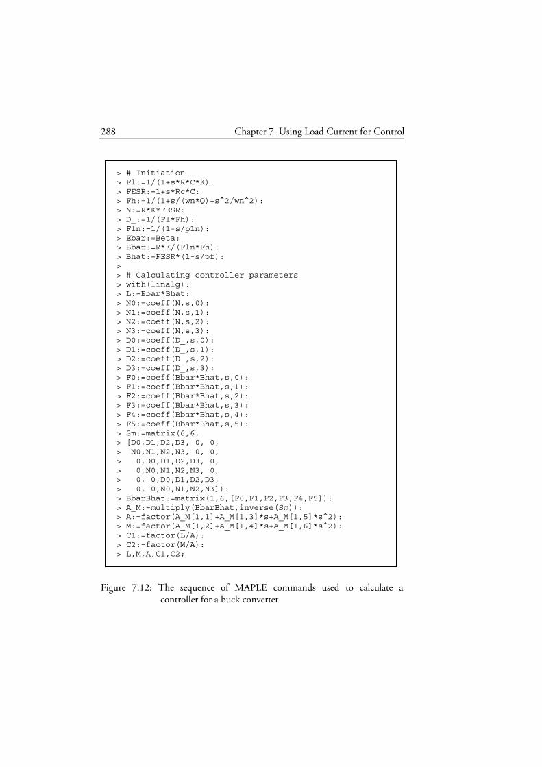
288 Chapter 7. Using Load Current for Control
> # Initiation > Fl:=1/(1+s*R*C*K): > FESR:=1+s*Rc*C: > Fh:=1/(1+s/(wn*Q)+s^2/wn^2): > N:=R*K*FESR: > D_:=1/(Fl*Fh): > Fln:=1/(1-s/p1n): > Ebar:=Beta: > Bbar:=R*K/(Fln*Fh): > Bhat:=FESR*(1-s/pf): > > # Calculating controller parameters > with(linalg): > L:=Ebar*Bhat: > N0:=coeff(N,s,0): > N1:=coeff(N,s,1): > N2:=coeff(N,s,2): > N3:=coeff(N,s,3): > D0:=coeff(D_,s,0): > D1:=coeff(D_,s,1): > D2:=coeff(D_,s,2): > D3:=coeff(D_,s,3): > F0:=coeff(Bbar*Bhat,s,0): > F1:=coeff(Bbar*Bhat,s,1): > F2:=coeff(Bbar*Bhat,s,2): > F3:=coeff(Bbar*Bhat,s,3): > F4:=coeff(Bbar*Bhat,s,4): > F5:=coeff(Bbar*Bhat,s,5): > Sm:=matrix(6,6, > [D0,D1,D2,D3, 0, 0, > N0,N1,N2,N3, 0, 0, > 0,D0,D1,D2,D3, 0, > 0,N0,N1,N2,N3, 0, > 0, 0,D0,D1,D2,D3, > 0, 0,N0,N1,N2,N3]): > BbarBhat:=matrix(1,6,[F0,F1,F2,F3,F4,F5]): > A_M:=multiply(BbarBhat,inverse(Sm)): > A:=factor(A_M[1,1]+A_M[1,3]*s+A_M[1,5]*s^2): > M:=factor(A_M[1,2]+A_M[1,4]*s+A_M[1,6]*s^2): > C1:=factor(L/A): > C2:=factor(M/A): > L,M,A,C1,C2;
Figure 7.12: The sequence of MAPLE commands used to calculate a controller for a buck converter

Chapter 7. Using Load Current for Control 289
,
11
111
1
)(
)()(
1
1
1
1
++−
++
−
−==
RCKpp
s
pRCKp
p
sCp
sA
sLsC
nff
n
fnβ
(7.78)
( ).
111)()(
11
)(
)()(
1
11
2
−++
++
−==
−
fnhESR
fn
ps
RCKpRsFsF
RCKpRCpK
sA
sMsC (7.79)
With )(1 sC and )(2 sC according to (7.78) and (7.79), the expressions for the dc gain and the position of all the poles and zeros of the closed loop system )(
2sG
coiv are independent of R if β and np1 are chosen not to depend on R . Note that both )(1 sC and )(2 sC are proper rational transfer functions.
Assume that fp is a negative real value with great absolute value. )(1 sC and )(2 sC can then be approximated in the frequency interval [ ]nω,0 by using (7.78), (7.79) and (7.26):
,)( 11 nCpsC β−≈ (7.80)
( )
.)()(
5.0'1
)()()(
11
1
2 RsFsF
pDmLC
TRC
RsFsF
RCpKsC
hESR
ncs
hESR
n
+−+
−=+
−≈−
(7.81)
It is seen from (7.81) and (7.80) that it is suitable to choose
( ) ,5.0'1 −−= DmLC
Tp c
sn (7.82)
290 Chapter 7. Using Load Current for Control
( ).
5.0'
11
1 −=−=
DmL
TCpc
sn
β (7.83)
None of β and np1 depends on R as required. Note that if )(sHi is equal to )(1 sF in (7.33), then the dc gain and the low-frequency pole in (7.33) are exactly the same as β and np1 in (7.83) and (7.82).
With the choices for β and np1 in (7.83) and (7.82), the following limits are obtained when fp tend to ∞− :
,1)(1 =sC (7.84)
.)()(
1)(2 RsFsF
sChESR
−= (7.85)
Note that )(2 sC in (7.85) is no longer a proper rational transfer function. From Figure 7.7, it is seen that the following control law is obtained if (7.84) and (7.85) are used:
,)(ˆ)(
1)(ˆ)(ˆ
2 svRsF
sisi occ−−= (7.86)
where )(sF is defined in (7.34).
The second step in designing the gain scheduling controller is to replace the parameter R in the control law (7.86) with the time-varying parameter
)(tRcal defined in (7.14) and the result is
.)(ˆ)(
1)(ˆ)(ˆ
)()(
1)(ˆ)(ˆ
22 sisF
sisvsRsF
sisi loadcocal
cc +=−−= (7.87)
By comparing (7.87) and (7.21), it is concluded that )(sHi should be equal to )(1 sF to obtain invariance for different loads. It has now been shown that this result could be obtained by applying gain scheduling.
Chapter 7. Using Load Current for Control 291
Output Impedance
In this subsection, the output impedance is derived for the case where the measured load current is used for control. The result is analyzed and compared with simulation results.
The approximate output impedance (6.44) is repeated here for convenience:
( ) ,)()()(ˆ)(ˆ
)(
2
2 sFsRKFsi
svsZ ESRl
olinj
oolout =
−= (7.88)
where K is defined in (7.26), )(sFl is defined in (7.27), and )(sFESR is defined in (7.28).
To obtain the output impedance of the closed loop system where (7.21) is used, the two input signals )(ˆ svg and )(ˆ
2 sic are set to zero in (7.24):
.1
)()(ˆ)(ˆ
1
)(ˆ)(ˆ
)()(ˆ)(ˆ
)(ˆ)(ˆ
)( 2
RsH
si
sv
si
svsH
si
sv
si
svsZ
ic
o
olinj
oi
c
o
inj
oout
−
+
−=−= (7.89)
(7.89) is rewritten by using (7.88) and (7.25):
( ).
)()()()(
)()()(1
)()()()(1
)()()()()()()(
1111 sHsFsFRsFKR
sFsHsF
sHsFsFsKF
sFsRKFsHsFsFsRKFsZ
ihESRl
ESRih
ihESRl
ESRlihESRlout
−−−− −−
=−
−−=
(7.90)
(7.90) is rewritten by using (7.32):
( )
( ) ( ).
5.0'1
)()()(1
)()()(1)(
−+−+
−=
DmLC
T
RCsHsFsFsC
sFsHsFsZ
cs
ihESR
ESRihout
(7.91)
292 Chapter 7. Using Load Current for Control
Figure 7.13: The output impedance of a buck converter controlled by (7.21). Dash-dotted line (): )(sHi =0 and R = minR . Dotted line (O):
)(sHi =0 and R = maxR . Solid line (+): )(sHi =1 and R = minR . Dashed line (x): )(sHi =1 and R = maxR . Note that the two last mentioned lines almost coincide. Points: Simulation with R = maxR and )(sHi equal to )(1 sFh in series with a second order filter.
Note that the denominator is exactly the same as in (7.33) and that the numerator is independent of R . The conclusions about invariance of R for the control-to-output transfer function are therefore also valid in this case. From (7.91), it is seen that the more )(sHi is in accordance with )(1 sFh , the lower is the output impedance. )(1 sFh is approximately equal to 1 at low frequencies. If (7.1) is used, i.e. )(sHi is equal to 1, the output impedance will be low at low frequencies.
Figure 7.13 shows the Bode plot for the output impedance in (7.91) when different )(sHi and loads are used. The parameter values used for the control-to-output transfer function are also used here. From the figure it is seen that for )(sHi =0, the output impedance is high at low frequencies.
101
102
103
104
-60
-40
-20
0
101
102
103
104
-100
-50
0
50
100
Frequency (Hz)
Pha
se (
deg)
; M
agni
tude
(dB
)
Chapter 7. Using Load Current for Control 293
When )(sHi is changed to 1, the output impedance is reduced at low frequencies and it becomes almost invariant for different loads. Simulation results are also plotted in Figure 7.13 and they are in good agreement with (7.91). The used simulation model will be presented at the end of this section. When )(sHi is changed to )(1 sFh in series with a second order Butterworth low-pass filter with corner frequency at five times the switching frequency, simulation results show (see Figure 7.13) that the output impedance is further decreased by approximately 20 dB for all the tested frequencies. Note that (7.91) is not valid for frequencies over half the switching frequency. It cannot therefore be used to predict what happens when there is a step change in the load, since the load current in this case consists of frequency components that are also over half the switching frequency.
Audio Susceptibility
In this subsection, the audio susceptibility is derived for the case where the measured load current is used for control. The result is analyzed and compared with simulation results.
The approximate audio susceptibility (6.47) is repeated here for convenience:
( ) ,)()()()(')(ˆ
)(ˆ
2
sFsFsKFsFDmL
DRT
sv
svhESRlfc
s
olg
o −=
(7.92)
where
( ) ( ),
24
21
12
23
21)( 2
22
sDTDD
sDTDD
sF ssf
+−−
−−−= (7.93)
K is defined in (7.26), )(sFl is defined in (7.27), )(sFESR is defined in (7.28), and )(sFh is defined in (7.29). )(sF f in (7.93) is used in this section and it is a Taylor polynomial of degree 2 of )(sF f in (6.48).
To obtain the audio susceptibility of the closed loop system where (7.21) is used, the two input signals )(ˆ siinj and )(ˆ
2 sic are set to zero in (7.24):
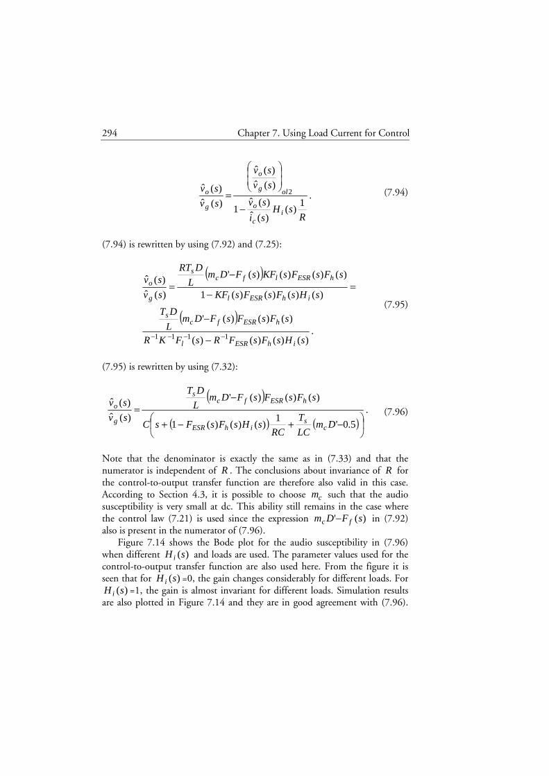
294 Chapter 7. Using Load Current for Control
.1
)()(ˆ)(ˆ
1
)(ˆ
)(ˆ
)(ˆ
)(ˆ 2
RsH
si
sv
sv
sv
sv
sv
ic
o
olg
o
g
o
−
= (7.94)
(7.94) is rewritten by using (7.92) and (7.25):
( )
( ).
)()()()(
)()()('
)()()()(1
)()()()('
)(ˆ
)(ˆ
1111 sHsFsFRsFKR
sFsFsFDmL
DT
sHsFsFsKF
sFsFsKFsFDmL
DRT
sv
sv
ihESRl
hESRfcs
ihESRl
hESRlfcs
g
o
−−−− −
−
=−
−=
(7.95)
(7.95) is rewritten by using (7.32):
( )( ) ( )
.
5.0'1
)()()(1
)()()('
)(ˆ
)(ˆ
−+−+
−=
DmLC
T
RCsHsFsFsC
sFsFsFDmL
DT
sv
sv
cs
ihESR
hESRfcs
g
o (7.96)
Note that the denominator is exactly the same as in (7.33) and that the numerator is independent of R . The conclusions about invariance of R for the control-to-output transfer function are therefore also valid in this case. According to Section 4.3, it is possible to choose cm such that the audio susceptibility is very small at dc. This ability still remains in the case where the control law (7.21) is used since the expression )(' sFDm fc − in (7.92) also is present in the numerator of (7.96).
Figure 7.14 shows the Bode plot for the audio susceptibility in (7.96) when different )(sHi and loads are used. The parameter values used for the control-to-output transfer function are also used here. From the figure it is seen that for )(sHi =0, the gain changes considerably for different loads. For
)(sHi =1, the gain is almost invariant for different loads. Simulation results are also plotted in Figure 7.14 and they are in good agreement with (7.96).
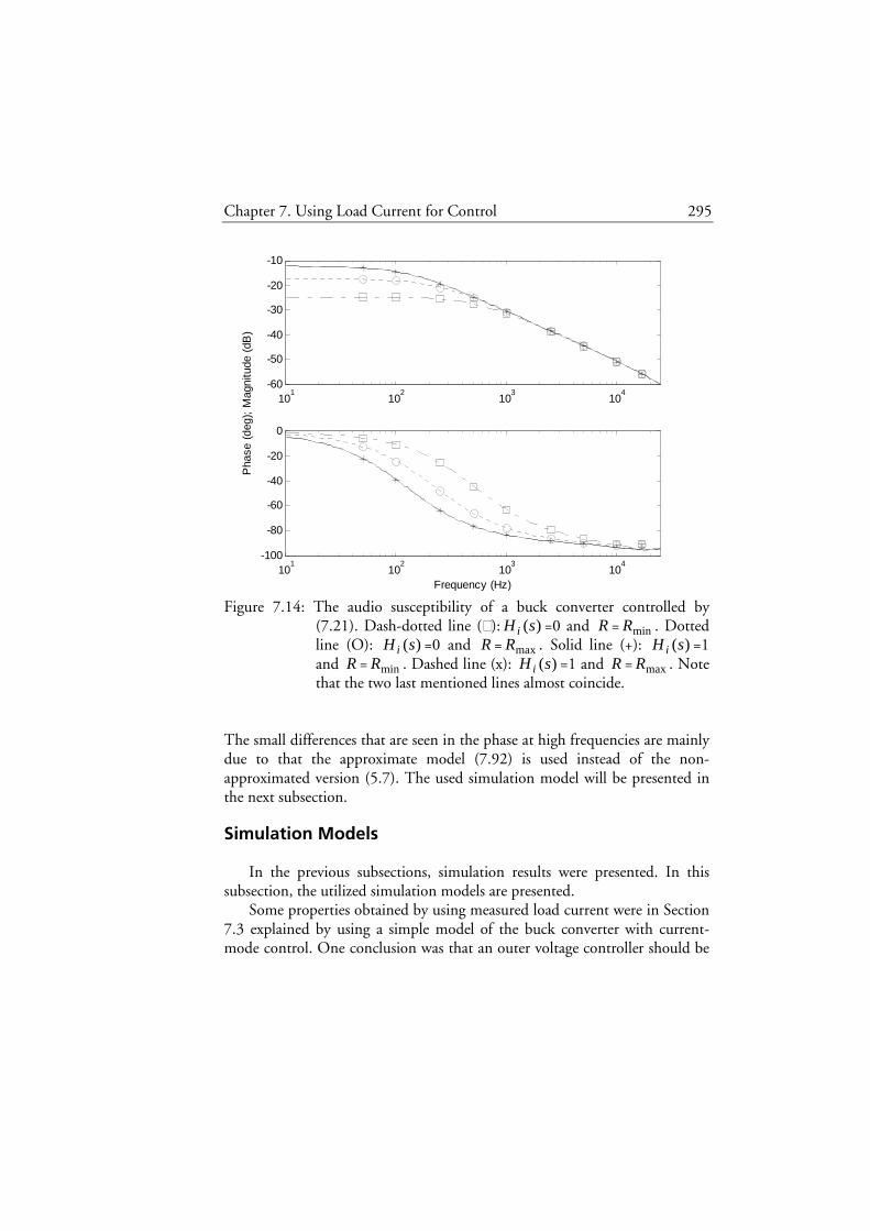
Chapter 7. Using Load Current for Control 295
Figure 7.14: The audio susceptibility of a buck converter controlled by (7.21). Dash-dotted line (): )(sHi =0 and R = minR . Dotted line (O): )(sHi =0 and R = maxR . Solid line (+): )(sHi =1 and R = minR . Dashed line (x): )(sHi =1 and R = maxR . Note that the two last mentioned lines almost coincide.
The small differences that are seen in the phase at high frequencies are mainly due to that the approximate model (7.92) is used instead of the non-approximated version (5.7). The used simulation model will be presented in the next subsection.
Simulation Models
In the previous subsections, simulation results were presented. In this subsection, the utilized simulation models are presented.
Some properties obtained by using measured load current were in Section 7.3 explained by using a simple model of the buck converter with current-mode control. One conclusion was that an outer voltage controller should be
101
102
103
104
-60
-50
-40
-30
-20
-10
101
102
103
104
-100
-80
-60
-40
-20
0
Frequency (Hz)
Pha
se (
deg)
; M
agni
tude
(dB
)
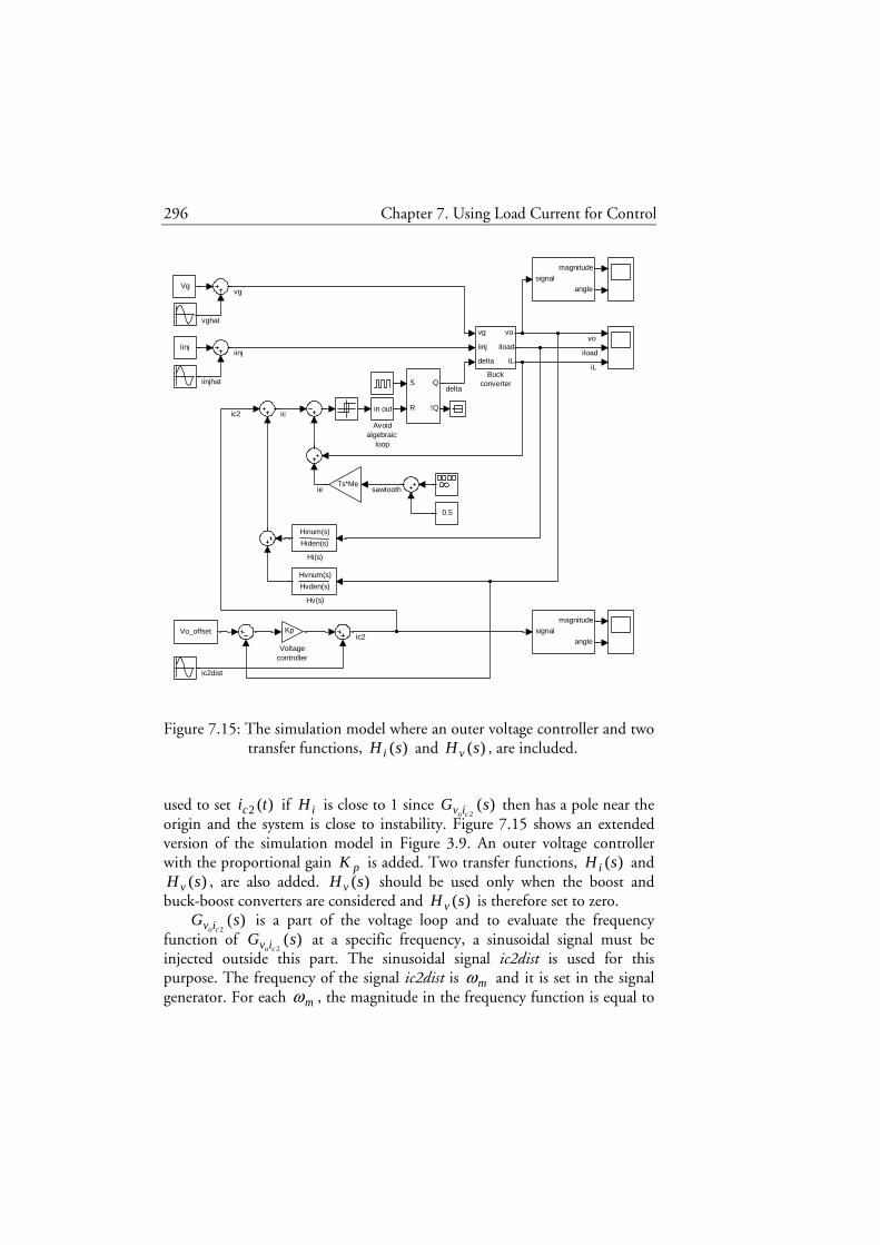
296 Chapter 7. Using Load Current for Control
Figure 7.15: The simulation model where an outer voltage controller and two
transfer functions, )(sHi and )(sH v , are included.
used to set )(2 tic if iH is close to 1 since )(2
sGcoiv then has a pole near the
origin and the system is close to instability. Figure 7.15 shows an extended version of the simulation model in Figure 3.9. An outer voltage controller with the proportional gain pK is added. Two transfer functions, )(sHi and
)(sH v , are also added. )(sH v should be used only when the boost and buck-boost converters are considered and )(sH v is therefore set to zero.
)(2
sGcoiv is a part of the voltage loop and to evaluate the frequency
function of )(2
sGcoiv at a specific frequency, a sinusoidal signal must be
injected outside this part. The sinusoidal signal ic2dist is used for this purpose. The frequency of the signal ic2dist is mω and it is set in the signal generator. For each mω , the magnitude in the frequency function is equal to
Kp Voltage
controller
Vg
S
R
Q
!Q
Iinj
Hvnum(s) Hvden(s)
Hv(s)
Hinum(s) Hiden(s)
Hi(s)
Ts*Me
signal
magnitude
angle
signal
magnitude
angle
Vo_offset
0.5
vg
iinj
delta
vo
iload
iL
Buck converter
in out
Avoid algebraic
loop
iinjhat
vo
iinj
vghat
vg
delta
iL
ie sawtooth
ic
iload
ic2dist
ic2
ic2

Chapter 7. Using Load Current for Control 297
the ratio of the magnitude of the signal vo to the magnitude of the signal ic2. The phase is equal to the phase of vo minus the phase of ic2. The magnitude and the phase of ic2 is not known since ic2 is partly set by the outer voltage controller. Fourier analysis must therefore be made of both ic2 and vo so that the components with frequency mω is obtained.
The simulation results for )(2
sGcoiv presented in Figure 7.11 are obtained
by using the simulation model in Figure 7.15. The parameters used in the simulation model presented in Section 3.5 are also used here. pK is set to 2 and the constant Vo_offset is adjusted manually so that the average value of the output voltage, oV , is equal to 5 V ( D =0.455).
The linearized system that is analyzed in this section has three input signals: )(ˆ tvg , )(ˆ tiinj , and )(ˆ
2 tic . )(ˆ2 tic is assumed to be zero in the cases
where the output impedance and the audio susceptibility are considered. If the signal generator for ic2dist is deactivated and either the signal generator for vghat or iinjhat is activated in the simulation model in Figure 7.15, the signal ic2 contains a component with frequency mω since the output voltage is fed back. One solution to this problem is to design the voltage controller such that the gain is zero at the frequency mω . This controller can be regarded as one with a notch filter included. One drawback of this solution is that the controller must be changed when mω is changed. Another drawback is that the time for each simulation can be long. We concluded previously in this section that according to the model derived in this section, the low-frequency pole is shifted a little to the left in the s-plane compared to what the simple model in Section 7.3 predicts. The system is therefore stable for
)(sHi =1 also without the outer voltage controller according to the model derived in this section. However, the stationary value of the output voltage is rather sensitive to changes in the stationary value of )(2 tic . Figure 7.16 shows a simulation model where the outer voltage controller is excluded. The magnitude and phase of the signal ic2 are set directly in the signal generator. The constant Ic2 is adjusted instead of Vo_offset. The frequency function of
)(2
sGcoiv has been obtained with the simulation model in Figure 7.16 but the
result is not presented here since it is almost the same as the result obtained with the simulation model in Figure 7.15. No difference can be seen without zooming the two Bode plots.
The simulation results for the output impedance presented in Figure 7.13 and the audio susceptibility presented in Figure 7.14 are obtained by using the simulation model in Figure 7.16.

298 Chapter 7. Using Load Current for Control
Figure 7.16: The simulation model where the outer voltage controller is
excluded.
7.5 Properties of the Boost Converter
In Section 6.3, approximate expressions for the boost converter with current-mode control were derived. In this section, these expressions are used to analyze how the control-to-output transfer function, the output impedance and the audio susceptibility are affected when using load current measurements to control the converter. An expression for the output voltage is first derived and this is then used to derive the three transfer functions. The results are compared with simulation results and a small difference is observed. This difference is explained for one case (the control-to-output transfer function) at the end of this section. In this section, it is assumed that the conditions in (6.101)-(6.107) are fulfilled since the approximate expressions derived in Section 6.3 may not be valid otherwise.
Vg
S
R
Q
!Q
Iinj
Hvnum(s) Hvden(s)
Hv(s)
Hinum(s) Hiden(s)
Hi(s)
Ts*Me
signal
magnitude
angle
Ic2
0.5
vg
iinj
delta
vo
iload
iL
Buck converter
in out
Avoid algebraic
loop
iinjhat
vo
iinj
vghat
vg
ic2hat
delta
iL
ie sawtooth
ic ic2
iload
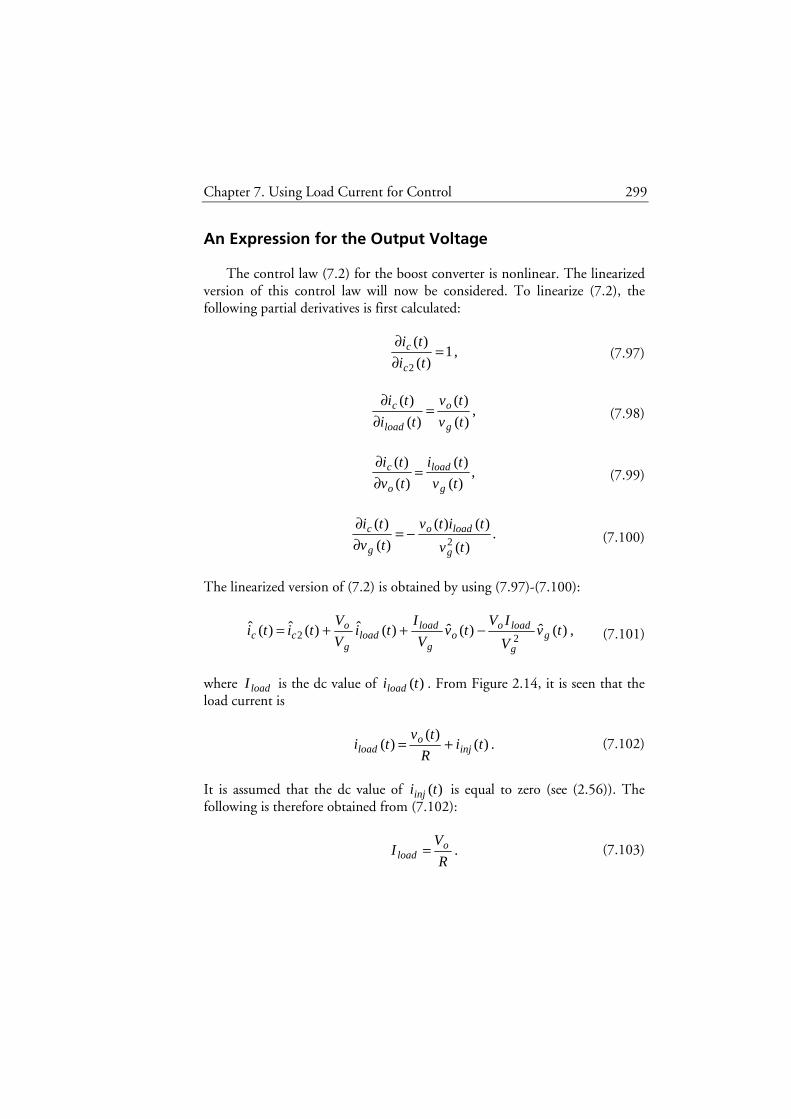
Chapter 7. Using Load Current for Control 299
An Expression for the Output Voltage
The control law (7.2) for the boost converter is nonlinear. The linearized version of this control law will now be considered. To linearize (7.2), the following partial derivatives is first calculated:
,1)(
)(
2
=∂∂
ti
ti
c
c (7.97)
,)(
)(
)(
)(
tv
tv
ti
ti
g
o
load
c =∂
∂ (7.98)
,)(
)(
)(
)(
tv
ti
tv
ti
g
load
o
c =∂∂
(7.99)
.)(
)()(
)(
)(2 tv
titv
tv
ti
g
loado
g
c −=∂∂
(7.100)
The linearized version of (7.2) is obtained by using (7.97)-(7.100):
,)(ˆ)(ˆ)(ˆ)(ˆ)(ˆ22 tv
V
IVtv
V
Iti
V
Vtiti g
g
loadoo
g
loadload
g
occ −++= (7.101)
where loadI is the dc value of )(tiload . From Figure 2.14, it is seen that the load current is
.)()(
)( tiR
tvti inj
oload += (7.102)
It is assumed that the dc value of )(tiinj is equal to zero (see (2.56)). The following is therefore obtained from (7.102):
.R
VI o
load = (7.103)
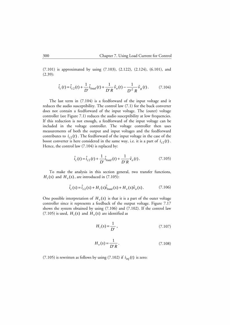
300 Chapter 7. Using Load Current for Control
(7.101) is approximated by using (7.103), (2.122), (2.124), (6.101), and (2.39):
.)(ˆ'
1)(ˆ
'
1)(ˆ
'
1)(ˆ)(ˆ
22 tvRD
tvRD
tiD
titi goloadcc −++= (7.104)
The last term in (7.104) is a feedforward of the input voltage and it
reduces the audio susceptibility. The control law (7.1) for the buck converter does not contain a feedforward of the input voltage. The (outer) voltage controller (see Figure 7.1) reduces the audio susceptibility at low frequencies. If this reduction is not enough, a feedforward of the input voltage can be included in the voltage controller. The voltage controller then uses measurements of both the output and input voltages and the feedforward contributes to )(2 tic . The feedforward of the input voltage in the case of the boost converter is here considered in the same way, i.e. it is a part of )(2 tic . Hence, the control law (7.104) is replaced by:
.)(ˆ'
1)(ˆ
'
1)(ˆ)(ˆ
2 tvRD
tiD
titi oloadcc ++= (7.105)
To make the analysis in this section general, two transfer functions,
)(sHi and )(sH v , are introduced in (7.105):
.)(ˆ)()(ˆ)()(ˆ)(ˆ2 svsHsisHsisi ovloadicc ++= (7.106)
One possible interpretation of )(sH v is that it is a part of the outer voltage controller since it represents a feedback of the output voltage. Figure 7.17 shows the system obtained by using (7.106) and (7.102). If the control law (7.105) is used, )(sHi and )(sH v are identified as
,'
1)(
DsHi = (7.107)
.'
1)(
RDsH v = (7.108)
(7.105) is rewritten as follows by using (7.102) if )(tiinj is zero:
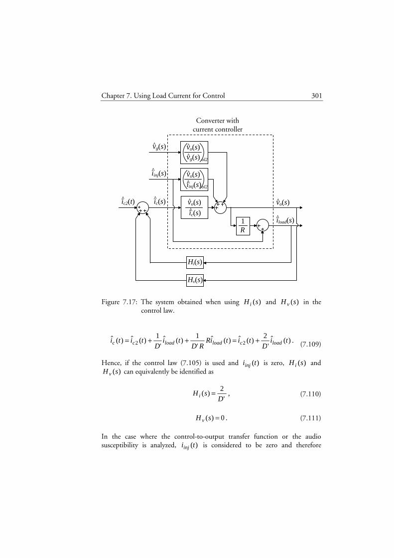
Chapter 7. Using Load Current for Control 301
Figure 7.17: The system obtained when using )(sHi and )(sH v in the
control law.
.)(ˆ'
2)(ˆ)(ˆ
'
1)(ˆ
'
1)(ˆ)(ˆ
22 tiD
titiRRD
tiD
titi loadcloadloadcc +=++=
(7.109)
Hence, if the control law (7.105) is used and )(tiinj is zero, )(sHi and )(sH v can equivalently be identified as
,'
2)(
DsHi = (7.110)
.0)( =sH v (7.111)
In the case where the control-to-output transfer function or the audio susceptibility is analyzed, )(tiinj is considered to be zero and therefore
iload(s)
ic2(t) ic(s)
Converter withcurrent controller
vo(s)
iinj(s)
iinj(s) ^
vo(s) ^
ol2
ic(s) ^
vo(s) ^
vg(s) ^
vo(s) ^
ol2
1 R
vg(s)
Hi(s)
Hv(s)
^
^
^ ^
^
^

302 Chapter 7. Using Load Current for Control
(7.110) and (7.111) can be used. The contribution )(ˆ)( svsH ov can always be moved to )(ˆ)( sisH loadi in these two cases and )(sH v can be considered to be zero. The control law (7.106) can then be replaced by (7.21) (see Figure 7.9).
The following is obtained from Figure 7.17:
.)(ˆ)(ˆ
)(ˆ)(ˆ
)(ˆ)(ˆ
)(ˆ)()(ˆ)(ˆ)()(ˆ
)(ˆ)(ˆ
)(ˆ)(ˆ
)(ˆ)(ˆ
)(ˆ)(ˆ
)(ˆ)(ˆ)(ˆ
)(ˆ
22
2
22
svsv
svsi
si
sv
svsHsiR
svsHsi
si
sv
svsv
svsi
si
svsi
si
svsv
g
olg
oinj
olinj
o
ovinjo
icc
o
g
olg
oinj
olinj
oc
c
oo
+
+
+
++
=
+
+=
(7.112)
An expression for the output voltage is obtained from (7.112):
,1
)()(ˆ)(ˆ
1)(ˆ)(ˆ
)(ˆ
)(ˆ)(ˆ)(ˆ
)()(ˆ)(ˆ
)(ˆ)(ˆ)(ˆ
)(ˆ
1
2
2
2
−
−
+
++=
RsH
si
svsv
sv
sv
sisi
svsH
si
svsi
si
svsv
c
og
olg
o
inj
olinj
oi
c
oc
c
oo
(7.113)
where
.)()()( sRHsHsH vi += (7.114)
Control-to-Output Transfer Function
In this subsection, the control-to-output transfer function is derived for the case where the measured load current is used for control. The result is analyzed and compared with simulation results. It is shown that the control-to-output transfer function cannot be made invariant for different loads in the frequency interval dc to half the switching frequency due to a right half plane zero. It is shown how to fix the poles and the rest of the zeros by designing a gain-scheduling controller.

Chapter 7. Using Load Current for Control 303
The approximate control-to-output transfer function (6.109) is repeated here for convenience:
,)()()()(')(ˆ)(ˆ
)( sFsFsFsKFRDsi
svsG RHPhESRl
c
oiv co
== (7.115)
where
( ),
5.0'
2
13
−+=
cs m
L
TRDK
(7.116)
,1
1)(
sRCKsFl +
= (7.117)
,'
1)(2RD
LssFRHP −= (7.118)
)(sFESR is defined in (7.28), )(sFh is defined in (7.29), and cm is defined
in (3.21). To obtain the control-to-output transfer function of the closed loop
system where (7.106) is used, the two input signals )(ˆ svg and )(ˆ siinj are set to zero in (7.113):
.1
)()(ˆ)(ˆ
1
)(ˆ)(ˆ
)(ˆ)(ˆ
2
RsH
si
svsi
sv
si
sv
c
o
c
o
c
o
−= (7.119)
(7.119) is rewritten by using (7.115):
.)()()()(')(
)()()('
)()()()()('1
)()()()('
)(ˆ)(ˆ
)(
1111
22
sHsFsFsFDRsFKR
sFsFsFD
sHsFsFsFsKFD
sFsFsFsKFRD
si
svsG
RHPhESRl
RHPhESR
RHPhESRl
RHPhESRl
c
oiv co
−−−− −
=−
==
(7.120)

304 Chapter 7. Using Load Current for Control
The (last) denominator in (7.120) is rewritten by using (7.117) and (7.116):
( )
( ) .5.0'
2)()()()(
2
'1
)()()()('
5.0'
2
)()()()('
)()()()(')(
3
1
31
111
1111
−
+
−+
=
−+−+
=−+
=−
−
−
−−−
−−−−
cs
RHPhESR
RHPhESR
cs
RHPhESR
RHPhESRl
mLC
TD
RCsHsFsFsF
DsC
sHsFsFsFDR
sCmL
TDR
sHsFsFsFDRsCKR
sHsFsFsFDRsFKR
(7.121)
According to a discussion previously in this section, )(sH v can be considered to be zero in the case where the control-to-output transfer function is analyzed. )(sH in (7.114) can therefore be replaced by )(sHi . (7.120) is rewritten by using this conclusion and (7.121):
( ) .5.0'
2)()()()(
2
'1
)()()(')(ˆ)(ˆ
)(
13
22
−
−
+
−+
•==
cs
iRHPhESR
RHPhESRc
oiv
mLC
TD
RCsHsFsFsF
DsC
sFsFsFDsi
svsG
co
(7.122)
A new variable, )(sF , is now introduced:
.)()()()( sFsFsFsF RHPhESR= (7.123)
The load resistance, R , occurs explicitly only at one place in (7.122) but it also occurs implicitly in )(sFRHP , see (7.118). The more )(sHi is in accordance with ( ))('2 sFD , the closer invariance for different loads is the denominator in the control-to-output transfer function. This is not easily
Chapter 7. Using Load Current for Control 305
made since )(1 sF has a right half plane pole and is unstable. If )(sF is approximately equal to 1 at low frequencies a good choice is to set )(sHi equal to '2 D which is the same as (7.110). )(sF is approximately equal to 1 at low frequencies if )(sFESR , )(sFh , and )(sFRHP are approximately equal to 1 at low frequencies. Condition (6.101) sets a lower limit for the corner frequency of )(sFESR . Condition (6.107) sets a lower limit for Q and therefore also a lower limit for the corner frequency of )(sFh (see upper plot in Figure 7.10). None of the conditions (6.101)-(6.107) sets an upper limit for L and therefore no lower limit for the corner frequency of )(sFRHP . However, there is a lower limit for the corner frequency of )(sFRHP in the design of the converter since a right half plane zero sets an upper limit for the bandwidth of the closed loop system. However, this bandwidth depends on the specifications of the converter. Therefore, from now on it will be assumed that corner frequency of )(sFRHP is much higher than the frequency of the low-frequency pole in (7.124).
If )(sHi is equal to 0, i.e. the measured load current is not used in the control law, the low-frequency pole in (7.122) is
( ) .5.0'2 3
1
−+−= cs m
LC
TD
RCp (7.124)
If )(sHi is equal to '2 D as in (7.110), the low-frequency pole in (7.122) is approximately
( ) .5.0'31 −−≈ cs m
LC
TDp (7.125)
There would be no approximation in (7.125) if )(sF was equal to 1. Since
)(sF is approximately equal to 1 at low frequencies, the low-frequency pole can be approximated according to (7.125).
It is seen from (7.122) that the dc gain is approximately inversely proportional to the distance between the low-frequency pole and the origin. Therefore, the dc gain approximately increases by the same degree as the first (lowest) corner frequency decreases if )(sHi is changed from 0 to '2 D .
Figure 7.18 shows the Bode plot for )(2
sGcoiv in (7.122) when different
)(sHi and loads, minR =1 Ω and maxR =4 Ω, are used. Except for R , the parameter values shown in Table 2.5 are used. cm is set to 2. From the figure

306 Chapter 7. Using Load Current for Control
Figure 7.18: The control-to-output transfer function of a boost converter controlled by (7.21). Dash-dotted line (): )(sHi =0 and R = minR . Dotted line (O): )(sHi =0 and R = maxR . Solid line (+): )(sHi = '2 D and R = minR . Dashed line (x):
)(sHi = '2 D and R = maxR .
it is seen that for )(sHi =0, the gain and phase shift changes considerably for different loads. For )(sHi = '2 D , the gain is almost invariant for different loads for low frequencies but not for high frequencies. Simulation results are also plotted in Figure 7.18 and they are in good agreement with (7.122). The small difference that is seen will be explained at the end of this section. The simulation model shown in Figure 7.15 is used, except the buck converter subsystem is replaced with the boost converter subsystem shown in Figure 2.14. The parameters used in the simulation model presented in Section 3.6 are also used here. pK is set to 2 and the constant Vo_offset is adjusted manually so that the average value of the duty cycle, D , is equal to 0.382. Note that the average value of the output voltage, oV , is a little higher in the case where R = maxR compared to the case where R = minR according to (2.124) and (2.122).
101
102
103
104
-40
-20
0
20
101
102
103
104
-250
-200
-150
-100
-50
0
Frequency (Hz)
Pha
se (
deg)
; M
agni
tude
(dB
)
Chapter 7. Using Load Current for Control 307
To see if it is possible to make the control-to-output transfer function closer to invariance for different loads compared to the choice )(sHi = '2 D , gain scheduling can be applied. The rest of this subsection will be devoted to applying gain scheduling and this will be made in the same way as in Section 7.4.
The first step is to design a controller by using model matching as if the resistance of the load is constant and known. The process to be controlled is
)(sGcoiv in (7.115):
,)(
)(
)()(
)()('
)(ˆ)(ˆ
)(11 sD
sN
sFsF
sFsKFRD
si
svsG
hl
RHPESR
c
oiv co
=== −− (7.126)
where
,)()(')( sFsKFRDsN RHPESR= (7.127)
.)()()( 11 sFsFsD hl−−= (7.128)
The position of the zero connected with )(sFESR does not depend on R . The same is true for the two high-frequency poles connected with )(sFh . However, the position of the low-frequency pole, 1p , connected with )(sFl depends on R . The position of the zero connected with )(sFRHP and the dc gain of )(sG
coiv also depend on R . The expressions for the dc gain and the position of all the poles and zeros
of the closed loop system )(2
sGcoiv should be independent of R . However,
this is not possible since the zero connected with )(sFRHP is in the right half side of the complex s-plane and such zeros cannot be moved, i.e. they must be placed at the same position as they have in the process (Chen, 1999, Section 9.3). To obtain a simple expression of the controller, the other zero and two poles are placed at the same position as the ESR zero and the two high-frequency poles in )(sG
coiv . The dc gain of )(2
sGcoiv is denoted β and the
position of the last pole in )(2
sGcoiv is denoted np1 . Hence, the low-
frequency pole, 1p , in )(sGcoiv is replaced by a new low-frequency pole,
np1 , in )(2
sGcoiv . The notation )(sF nl defined in (7.51) is used. )(
2sG
coiv can now be written as

308 Chapter 7. Using Load Current for Control
,)(
)(
)()(
)()(
)(ˆ)(ˆ
)(11
22 sB
sE
sFsF
sFsF
si
svsG
hnl
RHPESR
c
oiv co
===−−
β(7.129)
where
,)()()( sFsFsE RHPESRβ= (7.130)
.)()()( 11 sFsFsB hnl−−= (7.131)
The fraction )()(
2sNsG
coiv is now computed:
,
)(
)(
')()(
)()(')()(
)()(
)()(
)(
)(
)(
11
112
sB
sE
KRDsFsF
sFsKFRDsFsF
sFsF
sNsB
sE
sN
sG
hnl
RHPESRhnl
RHPESRiv co
=
===
−−
−−
β
β
(7.132)
where
,)( β=sE (7.133)
.')()()( 11 KRDsFsFsB hnl−−= (7.134)
The degree of the polynomial )(ˆ sB is chosen according to (7.62). For
our system, the degree condition is 23132)(ˆdeg =−−⋅≥sB . The degree of )(ˆ sB is here chosen to two and one root of )(ˆ sB is chosen to be equal to the
ESR zero since this simplifies the analysis of the controller design. The second root of )(ˆ sB is denoted fp and )(ˆ sB is written as
( ).1)()(ˆ 1spsFsB fESR−−= (7.135)
The polynomials )(sL , )(sM and )(sA are calculated by using the
same sequence of MAPLE commands as in Section 7.4 (see Figure 7.12) except for the initiation part which is replaced by the sequence shown in Figure 7.19. The following results are obtained:

Chapter 7. Using Load Current for Control 309
> # Initiation > Fl:=1/(1+s*R*C*K): > FESR:=1+s*Rc*C: > FRHP:=1-s*Lind/(R*Dp^2): > Fh:=1/(1+s/(wn*Q)+s^2/wn^2): > N:=R*Dp*K*FESR*FRHP: > D_:=1/(Fl*Fh): > Fln:=1/(1-s/p1n): > Ebar:=Beta: > Bbar:=R*Dp*K/(Fln*Fh): > Bhat:=FESR*(1-s/pf):
Figure 7.19: The initiation part of the sequence of MAPLE commands used to calculate a controller for a boost converter.
( ) ,11)(
−+=
fc p
sCsRsL β (7.136)
( )( )( )
( ) ,'
'11)(
1222
2221
nnf
nnnf
QpCKpLKCDR
DQssQRKCpRKCpsM
ω
ωω
+
++++= (7.137)
( )(
) ( )( ) .''
''''
1)(
11
221
21
222222
−+
+−−−+
•+=
nfnf
nf
c
pCpLKCDRDpRLKCp
RDCpKDRCpKDRLssCKDR
CsRsA
(7.138)
The resulting )(1 sC and )(2 sC are (after some rewriting)
,')(
'
1''
)(
)()(
2
112
121
1
f
RHPnn
f
n
p
RDs
RCK
sFpLpRD
p
sK
RC
LRD
D
Cp
sA
sLsC
−++−
−
+
−==
−β (7.139)
310 Chapter 7. Using Load Current for Control
( ).
')(')()(
11'
)(
)()(
2
112
11
2
−++−
++
−
==
−
f
RHPnnhESR
fn
p
RDs
RCK
sFpLpRDsFsF
RCKpRCpKD
sA
sMsC
(7.140)
With )(1 sC and )(2 sC according to (7.139) and (7.140), the expressions for the dc gain and the position of all the poles and one zeros of the closed loop system )(
2sG
coiv are independent of R if β and np1 are chosen not to depend on R . Note that both )(1 sC and )(2 sC are proper rational transfer functions.
Assume that fp is a negative real value with great absolute value. )(1 sC and )(2 sC can then be approximated in the frequency interval [ ]nω,0 by using (7.139), (7.140) and (7.116):
( ),
'
5.0'2
''
'
''
)(
12
321
12
121
1
LpRD
mC
TD
RC
LRD
D
Cp
LpRD
KRC
LRD
D
Cp
sC
n
csn
n
n
−
−++
−
=−
+−≈
−
β
β
(7.141)
( )( )
( )
( ) .')()(
5.0'''2
')()(
')(
12
13
121
1
2
LpRDsFsF
pmLC
TDRCDD
LpRDsFsF
RCpKDsC
nhESR
ncs
nhESR
n
−
+−+
−
=−
+−≈
−
(7.142)
It is seen from (7.142) and (7.141) that it is suitable to choose
Chapter 7. Using Load Current for Control 311
( ) ,5.0'31 −−= cs
n mLC
TDp (7.143)
( ).
5.0'
1'
21 −=−=
csn m
L
TD
Cp
Dβ (7.144)
None of β and np1 depends on R as required. Note that if )(sH i is equal to ( ))('2 sFD in (7.122), then the dc gain and the low-frequency pole in (7.122) are exactly the same as β and np1 in (7.144) and (7.143).
With the choices for β and np1 in (7.144) and (7.143), the following limits are obtained when fp tend to ∞− :
( )
,'
5.0'2
')(
12
32
1LpRD
mC
TD
RC
LRD
sCn
cs
−
−++= (7.145)
( ) .')()(
'2)(
122
LpRDsFsF
DsC
nhESR −−= (7.146)
Note that )(2 sC in (7.146) is no longer a proper rational transfer function. From Figure 7.7, it is seen that the following control law is obtained if (7.145) and (7.146) are used:
( )
.)(ˆ)()(
')(ˆ
'
2)(ˆ
'
)(ˆ)()(
'2)(ˆ2
'
'
)(ˆ)()(
'2)(ˆ5.0'
2'
)(ˆ
21
22
12
212
12
232
+
−+
=−
+
−+
=−
+
−++
=
svsFsF
Dsi
RC
L
LpRDsi
LpRD
svsFsF
DsiLp
RC
LRD
LpRD
svsFsF
Dsim
C
TD
RC
LRD
si
ohESR
cn
c
n
ohESR
cn
n
ohESR
ccs
c
(7.147)

312 Chapter 7. Using Load Current for Control
Figure 7.20: The control-to-output transfer function of a boost converter controlled by using gain scheduling. Solid line (+): R = minR . Dashed line (x): R = maxR .
The second step in designing the gain scheduling controller is to replace
the parameter R in the control law (7.147) with the time-varying parameter )(tRcal defined in (7.14).
Figure 7.20 shows the Bode plot for )(2
sGcoiv when the gain scheduling
controller ((7.147) with )(tR = )(tRcal ) and different loads, minR =1 Ω and
maxR =4 Ω, are used. Except for R , the parameter values shown in Table 2.5 are used. cm is set to 2. The output voltage should be filtered by
( ))()(1 sFsF hESR according to (7.147) but a second order Butterworth low-pass filter with corner frequency at the switching frequency is connected in series so that )(2 sC is proper. Note that this modifies the closeness to invariance for different loads a little near the switching frequency. (7.139) and (7.140) should have been used for )(1 sC and )(2 sC instead of (7.145) and (7.146) to obtain the invariance for different loads that was specified with proper )(2 sC . If Figure 7.20 is compared with Figure 7.18, where
101
102
103
104
-40
-20
0
20
101
102
103
104
-250
-200
-150
-100
-50
0
Frequency (Hz)
Pha
se (
deg)
; M
agni
tude
(dB
)
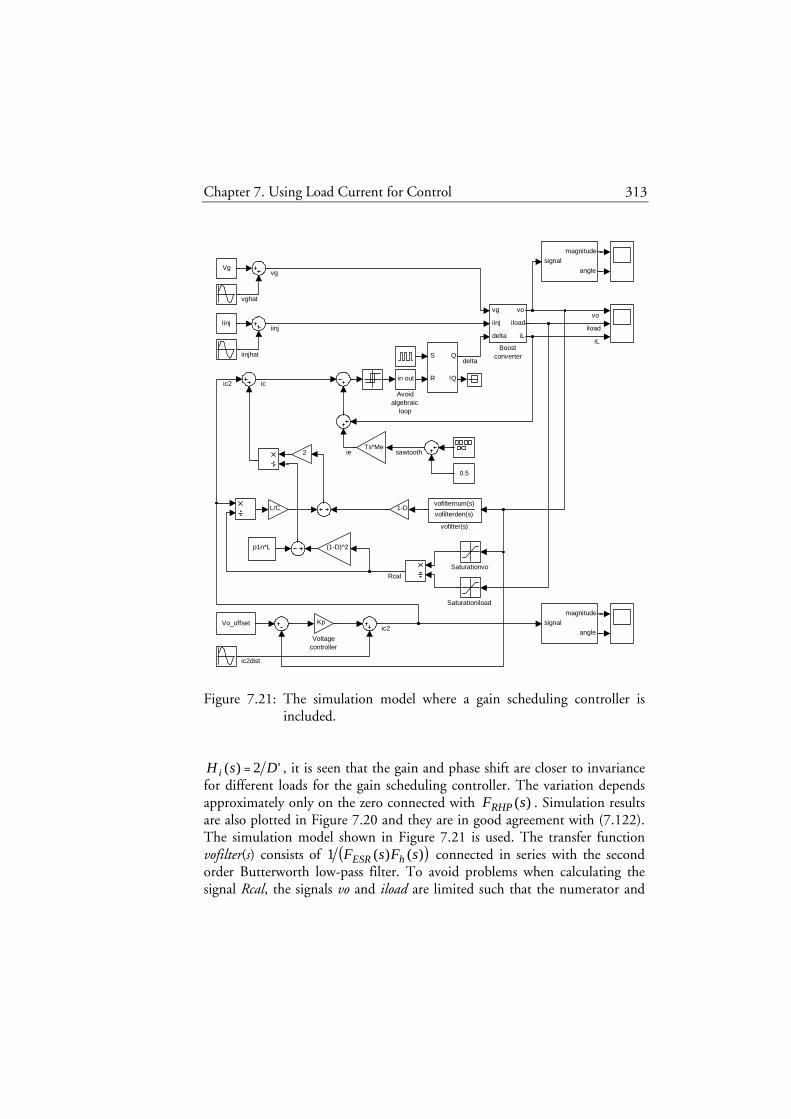
Chapter 7. Using Load Current for Control 313
Figure 7.21: The simulation model where a gain scheduling controller is
included.
)(sH i = '2 D , it is seen that the gain and phase shift are closer to invariance for different loads for the gain scheduling controller. The variation depends approximately only on the zero connected with )(sFRHP . Simulation results are also plotted in Figure 7.20 and they are in good agreement with (7.122). The simulation model shown in Figure 7.21 is used. The transfer function vofilter(s) consists of ( ))()(1 sFsF hESR connected in series with the second order Butterworth low-pass filter. To avoid problems when calculating the signal Rcal, the signals vo and iload are limited such that the numerator and
vofilternum(s) vofilterden(s)
vofilter(s)
L/C
2
(1-D)^2
1-D
Kp Voltage
controller
Vg
Saturationvo
Saturationiload
S
R
Q
!Q
Iinj
Ts*Me
signal
magnitude
angle
signal
magnitude
angle
p1n*L
Vo_offset
0.5
vg
iinj
delta
vo
iload
iL
Boost converter
in out
Avoid algebraic
loop
iinjhat
vo
iinj
vghat
vg
delta
iL
ie sawtooth
ic
iload
Rcal
ic2dist
ic2
ic2

314 Chapter 7. Using Load Current for Control
denominator in the fraction are greater than or equal to a small number. The parameters used in the simulation model used to obtain the simulation results in Figure 7.18 are also used here.
Output Impedance
In this subsection, the output impedance is derived for the case where the measured load current is used for control. The result is analyzed and compared with simulation results.
The approximate output impedance (6.118) is repeated here for convenience:
( ) ,)()()(ˆ)(ˆ
)(
2
2 sFsRKFsi
svsZ ESRl
olinj
oolout =
−= (7.148)
where K is defined in (7.116), )(sFl is defined in (7.117), and )(sFESR is defined in (7.28).
To obtain the output impedance of the closed loop system where (7.106) is used, the two input signals )(ˆ svg and )(ˆ
2 sic are set to zero in (7.113):
.1
)()(ˆ)(ˆ
1
)(ˆ)(ˆ
)()(ˆ)(ˆ
)(ˆ)(ˆ
)( 2
RsH
si
sv
si
svsH
si
sv
si
svsZ
c
o
olinj
oi
c
o
inj
oout
−
+
−=−= (7.149)
(7.149) is rewritten by using (7.148) and (7.115):
( ).
)()()()(')(
)()()()('1
)()()()()('1
)()()()()()()('
)(
1111 sHsFsFsFDRsFKR
sFsHsFsFD
sHsFsFsFsKFD
sFsRKFsHsFsFsFsKFRD
sZ
RHPhESRl
ESRiRHPh
RHPhESRl
ESRliRHPhESRl
out
−−−− −−
=−
−−
=
(7.150)
(7.150) is rewritten by using (7.121):

Chapter 7. Using Load Current for Control 315
( )
( ) ,5.0'
2)()()()(
2
'1
)()()()('1)(
13
−
−
+
−+
•−=
cs
RHPhESR
ESRiRHPhout
mLC
TD
RCsHsFsFsF
DsC
sFsHsFsFDsZ
(7.151)
where )(sH is defined in (7.114). Note that if (7.107) and (7.108) are used in (7.151) and if (7.110) is used in (7.122), then the denominators in (7.151) and (7.122) are exactly the same. From (7.151), it is seen that the more
)(sH i is in accordance with ( ))()('1 sFsFD RHPh , the lower is the output impedance. This is not easily made since )(sFRHP has a right half plane zero.
)()( sFsF RHPh is approximately equal to 1 at low frequencies so a good choice is to set )(sH i equal to '1 D which is the same as (7.107).
Figure 7.22 shows the Bode plot for the output impedance in (7.151) when different )(sH i , )(sH v , and loads are used. The parameter values used for the control-to-output transfer function are also used here. From the figure it is seen that when )(sH i and )(sH v are both zero, the output impedance is high at low frequencies. When )(sH i is changed to '1 D and
)(sH v is changed to ( )RD'1 , the output impedance is reduced at low frequencies but increased at high frequencies. However, the maximum impedance is decreased. The output impedance is not invariant for different loads at low frequencies due to )(sFRHP in the numerator of (7.151). Simulation results are also plotted in Figure 7.22 and they are in good agreement with (7.151) except at low frequencies in the case where
)(sH i = '1 D and )(sH v = ( )RD'1 . In this case, the phase shift and the slope of the magnitude curve are almost zero at low frequencies. It has also been noticed that the simulation results are very sensitive to changes in D in this case. None of these results are predicted by (7.151). Note that simulation results for the frequency 20 Hz are included in Figure 7.22. The simulation model shown in Figure 7.16 is used, except the buck converter subsystem is replaced with the boost converter subsystem shown in Figure 2.14. The parameters used in the simulation model presented in Section 3.6 are also used here. The constant Ic2 is adjusted manually so that the average value of the duty cycle, D , is equal to 0.382. Note once again that the average value of the output voltage, oV , is a little higher in the case where R = maxR compared to the case where R = minR according to (2.124) and (2.122).
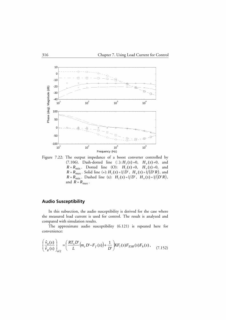
316 Chapter 7. Using Load Current for Control
Figure 7.22: The output impedance of a boost converter controlled by (7.106). Dash-dotted line (): )(sH i =0, )(sH v =0, and R = minR . Dotted line (O): )(sH i =0, )(sH v =0, and R = maxR . Solid line (+): )(sH i = '1 D , )(sH v = ( )RD'1 , and R = minR . Dashed line (x): )(sH i = '1 D , )(sH v = ( )RD'1 , and R = maxR .
Audio Susceptibility
In this subsection, the audio susceptibility is derived for the case where the measured load current is used for control. The result is analyzed and compared with simulation results.
The approximate audio susceptibility (6.121) is repeated here for convenience:
( ) ,)()()('
1)('
'
)(ˆ
)(ˆ
2
sFsFsKFD
sFDmL
DRT
sv
svhESRlfc
s
olg
o
+−=
(7.152)
101
102
103
104
-40
-30
-20
-10
0
10
101
102
103
104
-100
-50
0
50
100
Frequency (Hz)
Pha
se (
deg)
; M
agni
tude
(dB
)

Chapter 7. Using Load Current for Control 317
where
,122
1)( s
TsF s
f −= (7.153)
K is defined in (7.116), )(sFl is defined in (7.117), )(sFESR is defined in (7.28), and )(sFh is defined in (7.29). )(sF f in (7.153) is used in this section and it is a Taylor polynomial of degree 1 of )(sF f in (6.120).
To obtain the audio susceptibility of the closed loop system where (7.106) is used, the two input signals )(ˆ siinj and )(ˆ
2 sic are set to zero in (7.113):
.1
)()(ˆ)(ˆ
1
)(ˆ
)(ˆ
)(ˆ
)(ˆ 2
RsH
si
sv
sv
sv
sv
sv
c
o
olg
o
g
o
−
= (7.154)
(7.154) is rewritten by using (7.152) and (7.115):
( )
( ).
)()()()(')(
)()('
1)('
'
)()()()()('1
)()()('
1)('
'
)(ˆ
)(ˆ
1111 sHsFsFsFDRsFKR
sFsFRD
sFDmL
DT
sHsFsFsFsKFD
sFsFsKFD
sFDmL
DRT
sv
sv
RHPhESRl
hESRfcs
RHPhESRl
hESRlfcs
g
o
−−−− −
+−
=−
+−
= (7.155)
According to a discussion in the beginning of this section, )(sH v can be considered to be zero in the case where the audio susceptibility is analyzed.
)(sH in (7.114) can therefore be replaced by )(sH i . (7.155) is rewritten by using this conclusion and (7.121):

318 Chapter 7. Using Load Current for Control
( )
( ) .5.0'
2)()()()(
2
'1
)()('
1)('
'
)(ˆ
)(ˆ
13
−
−
+
−+
•
+−=
cs
iRHPhESR
hESRfcs
g
o
mLC
TD
RCsHsFsFsF
DsC
sFsFRD
sFDmL
DT
sv
sv
(7.156)
Note that the denominator is exactly the same as in (7.122). When )(sH i =0, an increase in R makes the numerator and the denominator in (7.156) both smaller and the audio susceptibility can in some cases be almost invariant for different loads at low frequencies. When )(sH i = '2 D , an increase in R makes the numerator smaller. The denominator is on the other hand almost invariant for different loads at low frequencies. The conclusion is that the audio susceptibility is closer to invariance for different loads when )(sH i =0 compared to when )(sH i = '2 D . For the buck converter, the conclusion was the opposite.
Figure 7.23 shows the Bode plot for the audio susceptibility in (7.156) when different )(sH i and loads are used. The parameter values used for the control-to-output transfer function are also used here. From the figure it is seen that for )(sH i = '2 D , the gain changes considerably for different loads at low frequencies. For )(sH i =0, the gain is almost invariant for different loads at low frequencies. Simulation results are also plotted in Figure 7.23 and they are in good agreement with (7.156). The simulation model used for the output impedance and its parameters are also used here.
The Difference Between the Simulation Results and the Model
From Figure 7.18, it is seen that there is a small difference between the simulation results and the model )(
2sG
coiv in (7.122) for the case where )(sH i = '2 D and R = minR . The reason for this difference is explained in
this subsection. The simulation results shown in Figure 7.18 were obtained with the
simulation model in Figure 7.15 (with the buck converter subsystem replaced). It is interesting to compare these simulation results with the ones
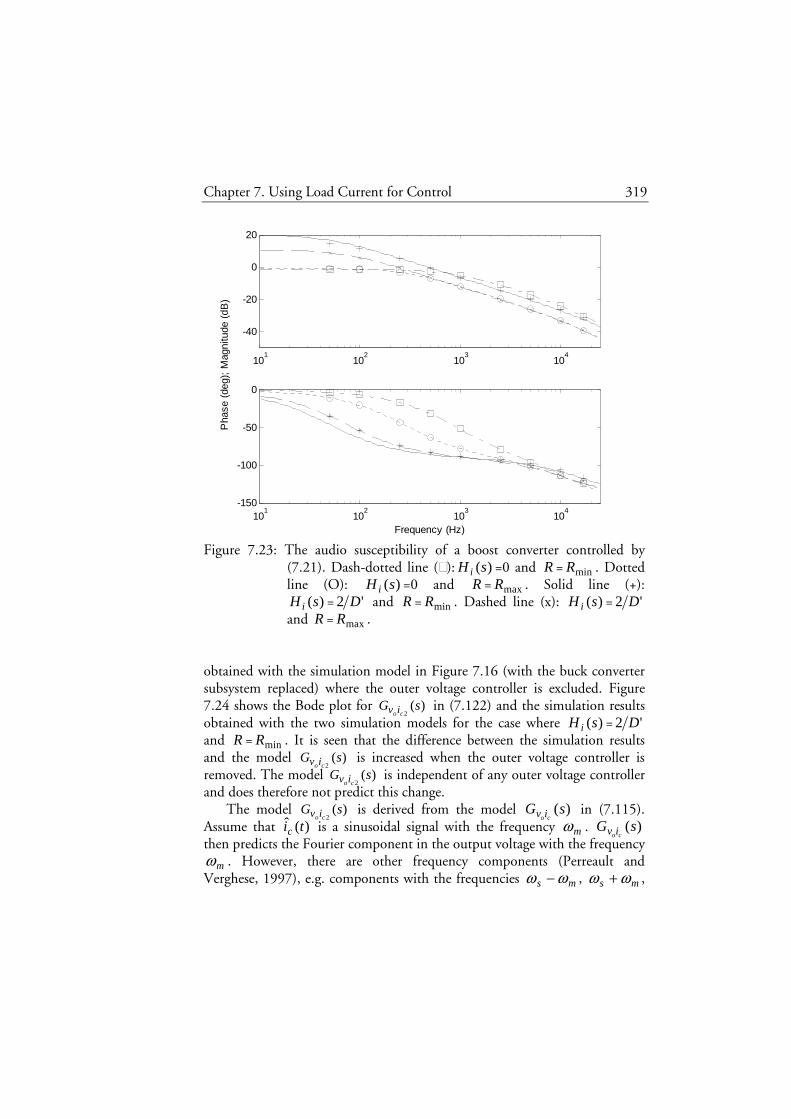
Chapter 7. Using Load Current for Control 319
Figure 7.23: The audio susceptibility of a boost converter controlled by (7.21). Dash-dotted line (): )(sH i =0 and R = minR . Dotted line (O): )(sH i =0 and R = maxR . Solid line (+):
)(sH i = '2 D and R = minR . Dashed line (x): )(sH i = '2 D and R = maxR .
obtained with the simulation model in Figure 7.16 (with the buck converter subsystem replaced) where the outer voltage controller is excluded. Figure 7.24 shows the Bode plot for )(
2sG
coiv in (7.122) and the simulation results obtained with the two simulation models for the case where )(sH i = '2 D and R = minR . It is seen that the difference between the simulation results and the model )(
2sG
coiv is increased when the outer voltage controller is removed. The model )(
2sG
coiv is independent of any outer voltage controller and does therefore not predict this change.
The model )(2
sGcoiv is derived from the model )(sG
coiv in (7.115). Assume that )(ˆ tic is a sinusoidal signal with the frequency mω . )(sG
coiv then predicts the Fourier component in the output voltage with the frequency
mω . However, there are other frequency components (Perreault and Verghese, 1997), e.g. components with the frequencies ms ωω − , ms ωω + ,
101
102
103
104
-40
-20
0
20
101
102
103
104
-150
-100
-50
0
Frequency (Hz)
Pha
se (
deg)
; M
agni
tude
(dB
)

320 Chapter 7. Using Load Current for Control
Figure 7.24: The control-to-output transfer function of a boost converter for the case where )(sH i = '2 D and R = minR . Solid line: model. +: simulation where the outer voltage controller is included and
pK =2. X: simulation where the outer voltage controller is excluded.
ms ωω −2 , ms ωω +2 , K , where sω is the switching frequency. The load current is proportional to the output voltage. )(ˆ tic is therefore not sinusoidal if the load current is used to affect )(ˆ tic . )(ˆ tic is sampled in current-mode control (see Section 3.3) and the sampling frequency is (in average) sω . Due to aliasing (Åström and Wittenmark, 1997, Section 7.4), the components in
)(ˆ tic with the frequencies ms ωω − , ms ωω + , ms ωω −2 , ms ωω +2 , K , affect the frequency component in )(ˆ zic with the frequency mω . This means that the model )(sG
coiv may not be valid if )(ˆ tic has components with frequencies higher than nω . The use of the model )(sG
coiv in the derivation of the model )(
2sG
coiv introduces an error since the model )(sGcoiv is used
in a situation where it is not valid. The following is obtained from Figure 7.15 if )(sH v =0:
101
102
103
104
-30
-20
-10
0
10
101
102
103
104
-250
-200
-150
-100
-50
0
Frequency (Hz)
Pha
se (
deg)
; M
agni
tude
(dB
)
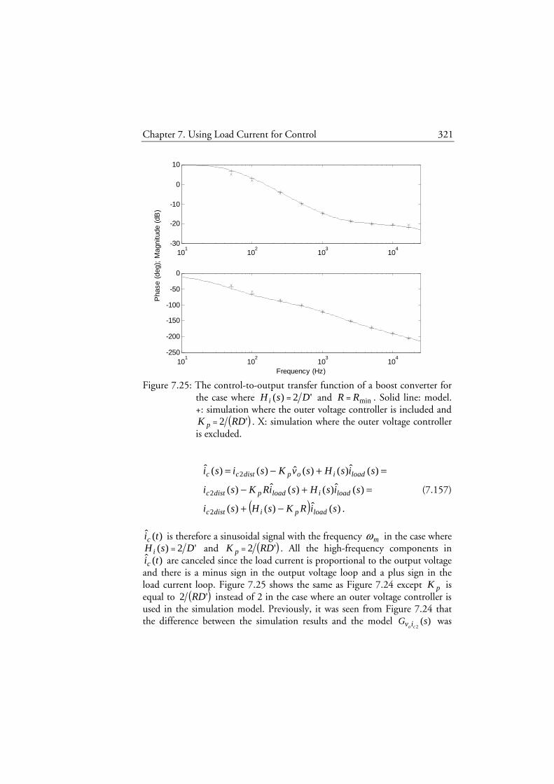
Chapter 7. Using Load Current for Control 321
Figure 7.25: The control-to-output transfer function of a boost converter for the case where )(sH i = '2 D and R = minR . Solid line: model. +: simulation where the outer voltage controller is included and
pK = ( )'2 RD . X: simulation where the outer voltage controller is excluded.
( ) .)(ˆ)()(
)(ˆ)()(ˆ)(
)(ˆ)()(ˆ)()(ˆ
2
2
2
siRKsHsi
sisHsiRKsi
sisHsvKsisi
loadpidistc
loadiloadpdistc
loadiopdistcc
−+
=+−
=+−=
(7.157)
)(ˆ tic is therefore a sinusoidal signal with the frequency mω in the case where
)(sH i = '2 D and pK = ( )'2 RD . All the high-frequency components in )(ˆ tic are canceled since the load current is proportional to the output voltage
and there is a minus sign in the output voltage loop and a plus sign in the load current loop. Figure 7.25 shows the same as Figure 7.24 except pK is equal to ( )'2 RD instead of 2 in the case where an outer voltage controller is used in the simulation model. Previously, it was seen from Figure 7.24 that the difference between the simulation results and the model )(
2sG
coiv was
101
102
103
104
-30
-20
-10
0
10
101
102
103
104
-250
-200
-150
-100
-50
0
Frequency (Hz)
Pha
se (
deg)
; M
agni
tude
(dB
)

322 Chapter 7. Using Load Current for Control
decreased when the outer voltage controller with pK =2 was included. By comparing Figure 7.24 and Figure 7.25, it is seen that the difference between the simulation results and the model )(
2sG
coiv decreases further when pK increases to ( )'2 RD . The high-frequency components in )(ˆ tic decreases continuously when pK increases continuously from 0 (no voltage controller) to ( )'2 RD .
From Figure 7.25, it is seen that there is a difference between the simulation results and the model )(
2sG
coiv in the case where pK is equal to ( )'2 RD even though the model )(sG
coiv is used in a situation where it should be valid. The difference is largest at low frequencies. If Figure 7.18 is zoomed, it is seen that difference in magnitude between the simulation results and the model )(
2sG
coiv is in order of 0.1 dB for the case where R = minR and )(sH i =0, i.e. the model )(sG
coiv is actually considered. Hence, it seems that )(
2sG
coiv is very sensitive to modeling errors in )(sGcoiv at low
frequencies. To investigate this, assume that the transfer function that correctly describes how )(ˆ tic affects (the component mω in) )(ˆ tvo in the simulation model is denoted by )(sG
coiv . Assume further that the transfer function that correctly describes how )(ˆ
2 tic affects (the component mω in) )(ˆ tvo in the simulation model is denoted by )(
2sG
coiv . The following are obtained from (7.119) and the fact that )(sH can be set to )(sH i :
,)()(1
)()(
12 −−=
RsHsG
sGsG
iiv
iviv
co
co
co (7.158)
.)()(1
)()(
12 −−=
RsHsG
sGsG
iiv
iviv
co
co
co (7.159)
Let )(s
coiv∆ and )(2
scoiv∆ denote the relative error in )(sG
coiv and )(
2sG
coiv , respectively, such that
( ) ,)()(1)( sGssGcococo iviviv ∆+= (7.160)
( ) .)()(1)(222
sGssGcococo iviviv ∆+= (7.161)
The following expression is obtained by using (7.161), (7.159), (7.158), and (7.160):
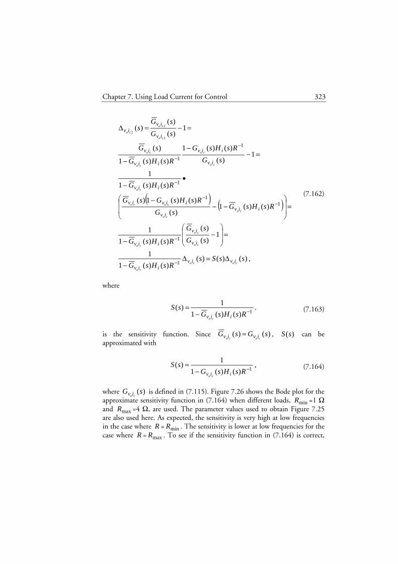
Chapter 7. Using Load Current for Control 323
( ) ( )
,)()()()()(1
1
1)(
)(
)()(1
1
)()(1)(
)()(1)(
)()(1
1
1)(
)()(1
)()(1
)(
1)(
)()(
1
1
11
1
1
1
2
2
2
ssSsRsHsG
sG
sG
RsHsG
RsHsGsG
RsHsGsG
RsHsG
sG
RsHsG
RsHsG
sG
sG
sGs
coco
co
co
co
co
co
co
coco
co
co
co
co
co
co
co
co
iviviiv
iv
iv
iiv
iiviv
iiviv
iiv
iv
iiv
iiv
iv
iv
iviv
∆=∆−
=
−
−
=
−−
−
•−
=−−
−
=−=∆
−
−
−−
−
−
−
(7.162)
where
.)()(1
1)(
1−−=
RsHsGsS
iiv co
(7.163)
is the sensitivity function. Since )()( sGsG
coco iviv ≈ , )(sS can be approximated with
,)()(1
1)(
1−−≈
RsHsGsS
iiv co
(7.164)
where )(sG
coiv is defined in (7.115). Figure 7.26 shows the Bode plot for the approximate sensitivity function in (7.164) when different loads, minR =1 Ω and maxR =4 Ω, are used. The parameter values used to obtain Figure 7.25 are also used here. As expected, the sensitivity is very high at low frequencies in the case where R = minR . The sensitivity is lower at low frequencies for the case where R = maxR . To see if the sensitivity function in (7.164) is correct,
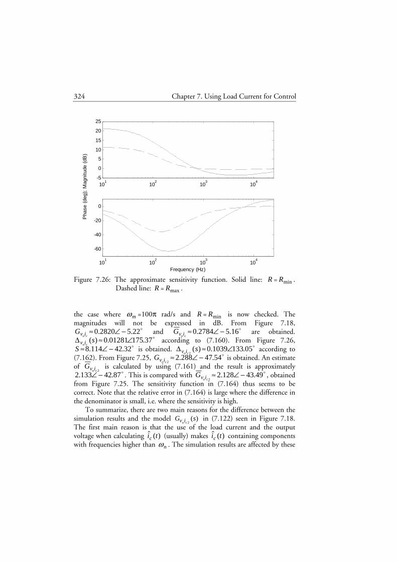
324 Chapter 7. Using Load Current for Control
Figure 7.26: The approximate sensitivity function. Solid line: R = minR . Dashed line: R = maxR .
the case where mω =100π rad/s and R = minR is now checked. The magnitudes will not be expressed in dB. From Figure 7.18,
coivG ≈ o22.52820.0 −∠ and coivG ≈ o16.52784.0 −∠ are obtained.
)(scoiv∆ ≈ o37.17501281.0 ∠ according to (7.160). From Figure 7.26,
S ≈ o32.42114.8 −∠ is obtained. )(2
scoiv∆ ≈ o05.1331039.0 ∠ according to
(7.162). From Figure 7.25, 2coivG ≈ o54.47288.2 −∠ is obtained. An estimate
of 2coivG is calculated by using (7.161) and the result is approximately
o87.42133.2 −∠ . This is compared with 2coivG ≈ o49.43128.2 −∠ , obtained
from Figure 7.25. The sensitivity function in (7.164) thus seems to be correct. Note that the relative error in (7.164) is large where the difference in the denominator is small, i.e. where the sensitivity is high.
To summarize, there are two main reasons for the difference between the simulation results and the model )(
2sG
coiv in (7.122) seen in Figure 7.18. The first main reason is that the use of the load current and the output voltage when calculating )(ˆ tic (usually) makes )(ˆ tic containing components with frequencies higher than nω . The simulation results are affected by these
101
102
103
104
-5
0
5
10
15
20
25
101
102
103
104
-60
-40
-20
0
Frequency (Hz)
Pha
se (
deg)
; M
agni
tude
(dB
)
Chapter 7. Using Load Current for Control 325
components but the model )(sGcoiv , which )(
2sG
coiv is derived from, is not designed to handle these components. The second main reason is that
)(2
sGcoiv is very sensitive to model errors in )(sG
coiv according to Figure 7.26.
Consider again the first main reason. As seen from Figure 7.25, the change in the simulation results is larger at low and high frequencies compared to at the frequencies in the middle. It seems to be rather complicated to analyze how the change varies with frequency since there seems to be several causal connections involved. However, it seems that the main reason for the relatively large change at very low frequencies is the high sensitivity to changes in )(sG
coiv according to Figure 7.26. It also seems that the main reason for the relatively large change at high frequencies is the significant increase in the magnitude of the component with frequency
ms ωω − in )(ˆ tic when mω increases towards nω .
7.6 Properties of the Buck-Boost Converter
In Section 6.4, approximate expressions for the buck-boost converter with current-mode control were derived. In this section, these expressions are used to analyze how the control-to-output transfer function, the output impedance and the audio susceptibility are affected when using load current measurements to control the converter. An expression for the output voltage is first derived and this is then used to derive the three transfer functions. The results are compared with simulation results. In this section, it is assumed that the conditions in (6.149)-(6.155) are fulfilled since the approximate expressions derived in Section 6.4 may not be valid otherwise. Many of the expressions in this section are identical to the ones obtained in Section 7.5.
An Expression for the Output Voltage
The control law (7.3) for the buck-boost converter is nonlinear. The linearized version of this control law will now be considered. To linearize (7.3), the following partial derivatives is first calculated:
,1)(
)(
2
=∂∂
ti
ti
c
c (7.165)

326 Chapter 7. Using Load Current for Control
,)(
)()(
)(
)(
tv
tvtv
ti
ti
g
go
load
c +=
∂∂
(7.166)
,)(
)(
)(
)(
tv
ti
tv
ti
g
load
o
c =∂∂
(7.167)
.)(
)()(
)(
)(2 tv
titv
tv
ti
g
loado
g
c −=∂∂
(7.168)
The linearized version of (7.3) is obtained by using (7.165)-(7.168):
.)(ˆ)(ˆ)(ˆ)(ˆ)(ˆ22 tv
V
IVtv
V
Iti
V
VVtiti g
g
loadoo
g
loadload
g
gocc −+
++= (7.169)
From Figure 2.20, it is seen that the load current is
.)()(
)( tiR
tvti inj
oload += (7.170)
It is assumed that the dc value of )(tiinj is equal to zero (see (2.56)). The following is therefore obtained from (7.170):
.R
VI o
load = (7.171)
(7.169) is approximated by using (7.171), (2.166), (2.168), (6.149), and (2.39):
.)(ˆ'
)(ˆ'
)(ˆ'
1)(ˆ)(ˆ
2
2
2 tvRD
Dtv
RD
Dti
Dtiti goloadcc −++= (7.172)
The last term in (7.172) is a feedforward of the input voltage and it is
here regarded as a part of )(2 tic (see Section 7.5). Hence, the control law (7.172) is replaced by:
Chapter 7. Using Load Current for Control 327
.)(ˆ'
)(ˆ'
1)(ˆ)(ˆ
2 tvRD
Dti
Dtiti oloadcc ++= (7.173)
To make the analysis in this section general, two transfer functions,
)(sH i and )(sH v , are introduced in (7.173):
.)(ˆ)()(ˆ)()(ˆ)(ˆ2 svsHsisHsisi ovloadicc ++= (7.174)
Figure 7.17 shows the system obtained by using (7.174) and (7.170). If the control law (7.173) is used, )(sH i and )(sH v are identified as
,'
1)(
DsH i = (7.175)
.'
)(RD
DsH v = (7.176)
(7.173) is rewritten as follows by using (7.170) if )(tiinj is zero:
.)(ˆ
'
1)(ˆ
)(ˆ'
)(ˆ'
1)(ˆ)(ˆ
2
2
tiD
Dti
tiRRD
Dti
Dtiti
loadc
loadloadcc
++
=++=(7.177)
Hence, if the control law (7.173) is used and )(tiinj is zero, )(sH i and
)(sH v can equivalently be identified as
,'
1)(
D
DsH i
+= (7.178)
.0)( =sH v (7.179)
In the case where the control-to-output transfer function or the audio susceptibility is analyzed, )(tiinj is considered to be zero and (7.178) and (7.179) can be used. The contribution )(ˆ)( svsH ov can always be moved to

328 Chapter 7. Using Load Current for Control
)(ˆ)( sisH loadi in these two cases and )(sH v can be considered to be zero. The control law (7.174) can then be replaced by (7.21) (see Figure 7.9).
(7.113) is an expression for the output voltage for the buck-boost converter since (7.174) and (7.170) are the same as (7.106) and (7.102), respectively.
Control-to-Output Transfer Function
In this subsection, the control-to-output transfer function is derived for the case where the measured load current is used for control. The result is analyzed and compared with simulation results.
The approximate control-to-output transfer function (6.157) is repeated here for convenience:
,)()()()(')(ˆ)(ˆ
)( sFsFsFsKFRDsi
svsG RHPhESRl
c
oiv co
== (7.180)
where
( ),
5.0'
1
13
−++=
cs m
L
TRDD
K (7.181)
,1
1)(
sRCKsFl +
= (7.182)
,'
1)(2RD
LDssFRHP −= (7.183)
)(sFESR is defined in (7.28), )(sFh is defined in (7.29), and cm is defined
in (3.21). To obtain the control-to-output transfer function of the closed loop
system where (7.174) is used, the two input signals )(ˆ svg and )(ˆ siinj are set to zero in (7.113):
Chapter 7. Using Load Current for Control 329
.1
)()(ˆ)(ˆ
1
)(ˆ)(ˆ
)(ˆ)(ˆ
2
RsH
si
sv
si
sv
si
sv
c
o
c
o
c
o
−= (7.184)
(7.184) is rewritten by using (7.180):
.)()()()(')(
)()()('
)()()()()('1
)()()()('
)(ˆ)(ˆ
)(
1111
22
sHsFsFsFDRsFKR
sFsFsFD
sHsFsFsFsKFD
sFsFsFsKFRD
si
svsG
RHPhESRl
RHPhESR
RHPhESRl
RHPhESRl
c
oiv co
−−−− −
=−
==
(7.185)
The (last) denominator in (7.185) is rewritten by using (7.182) and (7.181):
( ) ( )
( ) .5.0'
1)()()()(
1
'1
)()()()('
5.0'
1
)()()()('
)()()()(')(
3
1
31
111
1111
−
++
+−+
=
−+−++
=−+
=−
−
−
−−−
−−−−
cs
RHPhESR
RHPhESR
cs
RHPhESR
RHPhESRl
mLC
TD
RC
DsHsFsFsF
D
DsC
sHsFsFsFDR
sCmL
TDRD
sHsFsFsFDRsCKR
sHsFsFsFDRsFKR
(7.186)
According to a discussion previously in this section, )(sH v can be considered to be zero in the case where the control-to-output transfer function is analyzed. )(sH in (7.114) can therefore be replaced by )(sH i . (7.185) is rewritten by using this conclusion and (7.186):
330 Chapter 7. Using Load Current for Control
( ) .5.0'
1)()()()(
1
'1
)()()(')(ˆ)(ˆ
)(
13
22
−
−
++
+−+
•==
cs
iRHPhESR
RHPhESRc
oiv
mLC
TD
RC
DsHsFsFsF
D
DsC
sFsFsFDsi
svsG
co
(7.187)
A new variable, )(sF , is now introduced:
.)()()()( sFsFsFsF RHPhESR= (7.188)
The load resistance, R , occurs explicitly only at one place in (7.122) but it also occurs implicitly in )(sFRHP , see (7.183). The more )(sH i is in accordance with ( ) ( ))('1 sFDD+ , the closer invariance for different loads is the denominator in the control-to-output transfer function. This is not easily made since )(1 sF has a right half plane pole and is unstable. If )(sF is approximately equal to 1 at low frequencies a good choice is to set )(sH i equal to ( ) '1 DD+ which is the same as (7.178). )(sF is approximately equal to 1 at low frequencies if )(sFESR , )(sFh , and )(sFRHP are approximately equal to 1 at low frequencies. Condition (6.149) sets a lower limit for the corner frequency of )(sFESR . Condition (6.155) sets a lower limit for Q and therefore also a lower limit for the corner frequency of
)(sFh (see upper plot in Figure 7.10). None of the conditions (6.149)-(6.155) sets an upper limit for L and therefore no lower limit for the corner frequency of )(sFRHP .
Figure 7.27 shows the Bode plot for )(2
sGcoiv in (7.187) when different
)(sH i and loads, minR =1 Ω and maxR =4 Ω, are used. Except for R , the parameter values shown in Table 2.6 are used. cm is set to 2. From the figure it is seen that for )(sH i =0, the gain and phase shift changes considerably for different loads. For )(sH i = ( ) '1 DD+ , the gain is almost invariant for different loads for low frequencies but not for high frequencies. Simulation results are also plotted in Figure 7.27 and they are in good agreement with (7.187). The simulation model shown in Figure 7.15 is used, except the buck converter subsystem is replaced with the buck-boost converter subsystem shown in Figure 2.20. The parameters used in the simulation model
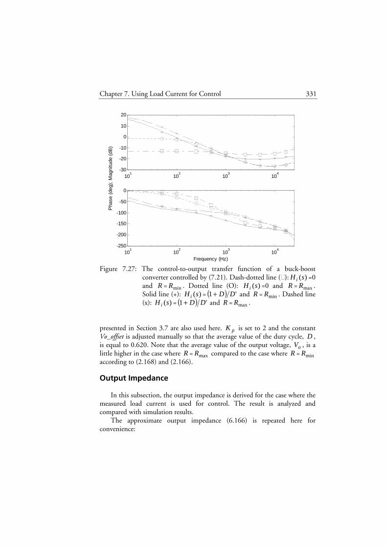
Chapter 7. Using Load Current for Control 331
Figure 7.27: The control-to-output transfer function of a buck-boost converter controlled by (7.21). Dash-dotted line (): )(sH i =0 and R = minR . Dotted line (O): )(sH i =0 and R = maxR . Solid line (+): )(sH i = ( ) '1 DD+ and R = minR . Dashed line (x): )(sH i = ( ) '1 DD+ and R = maxR .
presented in Section 3.7 are also used here. pK is set to 2 and the constant Vo_offset is adjusted manually so that the average value of the duty cycle, D , is equal to 0.620. Note that the average value of the output voltage, oV , is a little higher in the case where R = maxR compared to the case where R = minR according to (2.168) and (2.166).
Output Impedance
In this subsection, the output impedance is derived for the case where the measured load current is used for control. The result is analyzed and compared with simulation results.
The approximate output impedance (6.166) is repeated here for convenience:
101
102
103
104
-30
-20
-10
0
10
20
101
102
103
104
-250
-200
-150
-100
-50
0
Frequency (Hz)
Pha
se (
deg)
; M
agni
tude
(dB
)
332 Chapter 7. Using Load Current for Control
( ) ,)()()(ˆ)(ˆ
)(
2
2 sFsRKFsi
svsZ ESRl
olinj
oolout =
−= (7.189)
where K is defined in (7.181), )(sFl is defined in (7.182), and )(sFESR is defined in (7.28).
To obtain the output impedance of the closed loop system where (7.174) is used, the two input signals )(ˆ svg and )(ˆ
2 sic are set to zero in (7.113):
.1
)()(ˆ)(ˆ
1
)(ˆ)(ˆ
)()(ˆ)(ˆ
)(ˆ)(ˆ
)( 2
RsH
si
sv
si
svsH
si
sv
si
svsZ
c
o
olinj
oi
c
o
inj
oout
−
+
−=−= (7.190)
(7.190) is rewritten by using (7.189) and (7.180):
( ).
)()()()(')(
)()()()('1
)()()()()('1
)()()()()()()('
)(
1111 sHsFsFsFDRsFKR
sFsHsFsFD
sHsFsFsFsKFD
sFsRKFsHsFsFsFsKFRD
sZ
RHPhESRl
ESRiRHPh
RHPhESRl
ESRliRHPhESRl
out
−−−− −−
=−
−−
=
(7.191)
(7.191) is rewritten by using (7.186):
( )
( ) ,5.0'
1)()()()(
1
'1
)()()()('1)(
13
−
−
++
+−+
•−=
cs
RHPhESR
ESRiRHPhout
mLC
TD
RC
DsHsFsFsF
D
DsC
sFsHsFsFDsZ
(7.192)
where )(sH is defined in (7.114). From (7.192), it is seen that the more
)(sH i is in accordance with ( ))()('1 sFsFD RHPh , the lower is the output impedance. This is not easily made since )(sFRHP has a right half plane zero.

Chapter 7. Using Load Current for Control 333
Figure 7.28: The output impedance of a buck-boost converter controlled by (7.174). Dash-dotted line (): )(sH i =0, )(sH v =0, and R = minR . Dotted line (O): )(sH i =0, )(sH v =0, and R = maxR . Solid line (+): )(sH i = '1 D , )(sH v = ( )RDD ' , and R = minR . Dashed line (x): )(sH i = '1 D , )(sH v = ( )RDD ' , and R = maxR .
)()( sFsF RHPh is approximately equal to 1 at low frequencies so a good choice is to set )(sH i equal to '1 D which is the same as (7.175).
Figure 7.28 shows the Bode plot for the output impedance in (7.192) when different )(sH i , )(sH v , and loads are used. The parameter values used for the control-to-output transfer function are also used here. From the figure it is seen that when )(sH i and )(sH v are both zero, the output impedance is high at low frequencies. When )(sH i is changed to '1 D and
)(sH v is changed to ( )RDD ' , the output impedance is reduced at low frequencies but increased at high frequencies. However, the maximum impedance is decreased. The output impedance is not invariant for different loads at low frequencies due to )(sFRHP in the numerator of (7.192). Simulation results are also plotted in Figure 7.28 and they are in good agreement with (7.192) except at low frequencies in the case where
101
102
103
104
-40
-30
-20
-10
0
10
101
102
103
104
-100
-50
0
50
100
Frequency (Hz)
Pha
se (
deg)
; M
agni
tude
(dB
)

334 Chapter 7. Using Load Current for Control
)(sH i = '1 D and )(sH v = ( )RDD ' . The simulation model shown in Figure 7.16 is used, except the buck converter subsystem is replaced with the buck-boost converter subsystem shown in Figure 2.20. The parameters used in the simulation model presented in Section 3.7 are also used here. The constant Ic2 is adjusted manually so that the average value of the duty cycle, D , is equal to 0.620. To obtain D =0.620 in steady state, not just Ic2 must be adjusted but also the initial voltage across the output capacitor. The initial voltage must be close to the output voltage corresponding to D =0.620. The initial values of the states in the simulator are set by using a powergui block. Note that this was not necessary for the boost converter where the duty cycle converged to the correct value even if the initial values were zero. The model that we derived for the buck-boost converter, which predicted stability, is a small-signal model and may result in erroneous conclusions if the deviations from the specified operating point are large.
Audio Susceptibility
In this subsection, the audio susceptibility is derived for the case where the measured load current is used for control. The result is analyzed and compared with simulation results.
The approximate audio susceptibility (6.178) is repeated here for convenience:
( ) ,)()()()('
)(''
)(ˆ
)(ˆ
21
2
sFsFsDKFsFD
DsFDm
L
DRT
sv
sv
hESRlffcs
olg
o
+−
=
(7.193)
where
( )
,12
23
21)(1 s
DTDDsF s
f−
−−= (7.194)
,2
'1)(2 s
TDsF s
f += (7.195)

Chapter 7. Using Load Current for Control 335
K is defined in (7.181), )(sFl is defined in (7.182), )(sFESR is defined in (7.28), and )(sFh is defined in (7.29). )(1 sF f and )(2 sF f in (7.194) and (7.195) are used in this section and they are Taylor polynomials of degree 1 of )(1 sF f and )(2 sF f in (6.176) and (6.177).
To obtain the audio susceptibility of the closed loop system where (7.174) is used, the two input signals )(ˆ siinj and )(ˆ
2 sic are set to zero in (7.113):
.1
)()(ˆ)(ˆ
1
)(ˆ
)(ˆ
)(ˆ
)(ˆ 2
RsH
si
sv
sv
sv
sv
sv
c
o
olg
o
g
o
−
= (7.196)
(7.196) is rewritten by using (7.193) and (7.180):
( )
( ).
)()()()(')(
)()()('
)(''
)()()()()('1
)()()()('
)(''
)(ˆ
)(ˆ
1111
21
21
sHsFsFsFDRsFKR
sFsDFsFRD
DsFDm
L
DT
sHsFsFsFsKFD
sFsFsDKFsFD
DsFDm
L
DRT
sv
sv
RHPhESRl
hESRffcs
RHPhESRl
hESRlffcs
g
o
−−−− −
+−
=−
+−
=
(7.197)
According to a discussion in the beginning of this section, )(sH v can be considered to be zero in the case where the audio susceptibility is analyzed.
)(sH in (7.114) can therefore be replaced by )(sH i . (7.197) is rewritten by using this conclusion and (7.186):

336 Chapter 7. Using Load Current for Control
( )
( ) .5.0'
1)()()()(
1
'1
)()()('
)(''
)(ˆ
)(ˆ
13
21
−
−
++
+−+
•
+−=
cs
iRHPhESR
hESRffcs
g
o
mLC
TD
RC
DsHsFsFsF
D
DsC
sFsDFsFRD
DsFDm
L
DT
sv
sv
(7.198)
When )(sH i =0, an increase in R makes the numerator and the denominator in (7.198) both smaller and the audio susceptibility can in some cases be almost invariant for different loads at low frequencies. When
)(sH i = ( ) '1 DD+ , an increase in R makes the numerator smaller. The denominator is on the other hand almost invariant for different loads at low frequencies. The conclusion is that the audio susceptibility is closer to invariance for different loads when )(sH i =0 compared to when
)(sH i = ( ) '1 DD+ . Figure 7.29 shows the Bode plot for the audio susceptibility in (7.198)
when different )(sH i and loads are used. The parameter values used for the control-to-output transfer function are also used here. From the figure it is seen that for )(sH i = ( ) '1 DD+ , the gain changes considerably for different loads at low frequencies. For )(sH i =0, the gain is almost invariant for different loads at low frequencies. Simulation results are also plotted in Figure 7.29 and they are in good agreement with (7.198). The simulation model used for the output impedance and its parameters are also been used here.
7.7 Summary and Concluding Remarks
The output voltage and the inductor current are measured in the case where current-mode control is used. Some properties that can be obtained when the controller also uses load current measurements were in this chapter analyzed and some of the previous works were reviewed.
The main results are summarized here.
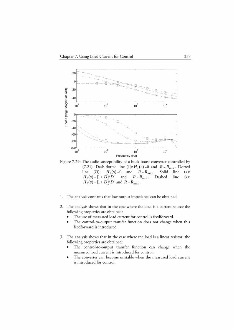
Chapter 7. Using Load Current for Control 337
Figure 7.29: The audio susceptibility of a buck-boost converter controlled by (7.21). Dash-dotted line (): )(sH i =0 and R = minR . Dotted line (O): )(sH i =0 and R = maxR . Solid line (+):
)(sH i = ( ) '1 DD+ and R = minR . Dashed line (x): )(sH i = ( ) '1 DD+ and R = maxR .
1. The analysis confirms that low output impedance can be obtained. 2. The analysis shows that in the case where the load is a current source the
following properties are obtained: • The use of measured load current for control is feedforward. • The control-to-output transfer function does not change when this
feedforward is introduced. 3. The analysis shows that in the case where the load is a linear resistor, the
following properties are obtained: • The control-to-output transfer function can change when the
measured load current is introduced for control. • The converter can become unstable when the measured load current
is introduced for control.
101
102
103
104
-40
-20
0
20
101
102
103
104
-100
-80
-60
-40
-20
0
Frequency (Hz)
Pha
se (
deg)
; M
agni
tude
(dB
)

338 Chapter 7. Using Load Current for Control
• The control-to-output transfer function can be almost invariant for different linear resistive loads if the measured load current is used for control. This is especially the case for the buck converter.
• The use of measured load current for control is not feedforward. It can instead be seen as gain scheduling.
Expressions for the control-to-output transfer function, the output
impedance, and the audio susceptibility were derived from the expressions obtained in Chapter 6. There are differences between simulation results and the predictions of these derived expressions in the case where the boost or the buck-boost converter is considered. The difference was examined in one specific case. We concluded that there are two main reasons for the difference. The first main reason is that components with frequencies higher than half the switching frequency affects the control signal and the expression is derived without taking these into account. The second main reason is that the expression can be very sensitive to errors in the used expressions from Chapter 6. The differences in the other cases are probably also due to these two reasons.
The approximate expressions obtained in Chapter 6 were used as a starting point in Section 7.4, 7.5, and 7.6. This is not the best way to derive reliable expressions for the closed loop system obtained when the load current is used for control. Instead, the non-approximate expressions should have been used as a starting point and the derived expressions for the closed loop system should have been approximated afterwards.
As an example, consider the control-to-output transfer function )(2
sGcoiv
for the buck converter, (7.33). The denominator is:
( ) ( ) .5.0'1
)()()(1
−+−+ DmLC
T
RCsHsFsFsC c
sihESR (7.199)
If the non-approximate expressions are used and the approximation is made afterwards, the following denominator is obtained:
( ) ( ) .5.0'1
)()(1
−+−+ DmLC
T
RCsHsFsC c
sih (7.200)
If )(sH i is equal to 0, there is no difference between (7.199) and (7.200). It was shown in Section 7.4 that if )(sH i is equal to 1, the absolute value of the

Chapter 7. Using Load Current for Control 339
second term is much smaller than the absolute value of the first term, s , in the (largest) parenthesis in (7.199). The difference between (7.199) and (7.200) is therefore negligible in the case where )(sH i is equal to 1 if the values of the denominators are considered. However, the two denominators give two different answers to the question of how to set )(sH i to obtain (total) invariance for different loads. At high frequencies, it is a large difference between the two answers )(sH i = ( ))()(/1 sFsF hESR and
)(sH i = )(/1 sFh . The results in Section 7.4, 7.5, and 7.6 are planned to be remade in such
a way that the approximations are made after the derivations. The new results are planned to be published in the Ph.D. dissertation of the author of this thesis.

341
Chapter 8 Summary
The work presented in this thesis is summarized in this chapter. Suggestions for future work are also summarized.
8.1 Results
This section explains which major models were obtained and how they were derived. The main conclusions are also presented. However, the method used to verify the obtained models is first explained.
Verification
Evaluation of a converter by means of a network analyzer is common and this is one of the reasons for the interest in models that can predict the frequency functions.
To verify the derived small-signal models, the frequency functions predicted by them were compared with simulation results. Switched (large-signal) simulation models were utilized and the output voltage then consists of several Fourier components. To obtain the frequency function, one frequency at the time was evaluated. A sinusoidal signal with frequency mω was injected and only the Fourier component with frequency mω in the output voltage was considered. A network analyzer also just considers this Fourier component.
The control signal can be considered to be sampled with the switching frequency. The frequency functions were therefore only evaluated for the frequency interval dc to half the switching frequency.

342 Chapter 8. Summary
State-Space averaging
State-space averaging was used to derive linear continuous-time time-invariant models for the buck, boost, and buck-boost converters. The control-to-output transfer function, the output impedance, and the audio susceptibility were extracted from each one of these models. We concluded that these transfer functions are in good agreement with the simulation results.
Current-Mode Control
The Ridley and Tan models were applied to the buck converter with current-mode control. We concluded that the obtained control-to-output transfer functions and the output impedances are in good agreement with the simulation results but the obtained audio susceptibilities are not.
The Ridley model was also applied to the boost and buck-boost converters with current-mode control. Also in these cases, we concluded that the obtained audio susceptibilities are not in good agreement with the simulation results.
The high-frequency extensions in the Ridley and Tan models are based on an accurate control-to-current transfer function, which is derived with the assumption that the changes in the input and output voltages are negligible. The actual changes in the input and output voltages are in the Ridley and Tan models taken into consideration by including two feedforward gains, fk and rk . These gains are designed such that the dc gain should be correct. This design results in modeling errors, especially for the audio susceptibilities at high frequencies. The reason is that the amplitude of the perturbation in the input voltage does not decrease at high frequencies since the injection signal from the network analyzer affects the input voltage directly. However, when the control-to-output transfer function and the output impedance are considered, the input voltage is not affected and the changes in the output voltage is negligible at high frequencies due to the low-pass character of the output filter of the converters.
A Novel Model
A novel model for the audio susceptibility of converters with current-mode control was derived by treating the changes in the input and output voltages in a more refined way. The novel model was applied to the buck,
Chapter 8. Summary 343
boost and buck-boost converters. We concluded that the obtained audio susceptibilities are in good agreement with simulation results at high frequencies but in some cases not at low frequencies. For one of these cases, we concluded that the reason for the poor predictions is that the novel model is very sensitive at low frequencies to errors in some of models that it is based on.
Improved Models
The novel model was used to improve the Ridley and Tan models. The feedforward gains fk were changed such that the two models became equal to the novel model. However, we used a combined model instead of the novel model in the cases where the novel model makes poor low-frequency predictions. To obtain the combined model, the low-frequency properties of the (original) Ridley model was combined with the high-frequency properties of the novel model
One disadvantage with the improved models is that fk in some cases was an unstable transfer function.
Approximations of Obtained Expressions
The control-to-output transfer functions, the output impedances, and the audio susceptibilities obtained from the (improved) Ridley model were approximated. To be able to do this, several assumptions were introduced.
Using Load Current for Control
The output voltage and the inductor current are measured in the case where current-mode control is used. Some properties that can be obtained when the controller also uses load current measurements were analyzed. The control-to-output transfer function, the output impedance, and the audio susceptibility were derived for each treated converter topology: buck, boost, and buck-boost. The main conclusions are presented here.
1. The analysis confirms that low output impedance can be obtained. 2. The analysis shows that in the case where the load is a current source the
following properties are obtained: • The use of measured load current for control is feedforward.

344 Chapter 8. Summary
• The control-to-output transfer function does not change when this feedforward is introduced.
3. The analysis shows that in the case where the load is a linear resistor, the
following properties are obtained: • The control-to-output transfer function can change when the
measured load current is introduced for control. • The converter can become unstable when the measured load current
is introduced for control. • The control-to-output transfer function can be almost invariant for
different linear resistive loads if the measured load current is used for control. This is especially the case for the buck converter.
• The use of measured load current for control is not feedforward. It can instead be seen as gain scheduling.
The difference between the simulation results and the derived control-to-
output transfer functions, the output impedances, and the audio susceptibilities are is some cases significant. For one specific case, we concluded that the reasons for this are the fact that the measured load current contains components with frequencies higher than half the switching frequency and high sensitivity to errors in the models used as a starting point in the analysis.
8.2 Future Work
Suggestions for future work are summarized here.
• Modify the novel model in such a way that the low-frequency predictions are not so sensitive to errors.
• Find out how to improve the Ridley model without using unstable transfer functions. An idea how to do this was presented in Section 5.5.
• Perform experiments to validate the main results in Chapter 7. • Find out suitable methods to identify the load and use the result in an
adaptive controller in cases where the load is more complex. This was discussed in Section 1.2.

345
Chapter 9 Errata for Three Papers
Errata for the following three conference papers are presented in this chapter.
1. Johansson, B. and Lenells, M. (2000), Possibilities of obtaining
small-signal models of DC-to-DC power converters by means of system identification, IEEE International Telecommunications Energy Conference, pp. 65-75, Phoenix, Arizona, USA, 2000.
2. Johansson, B. (2002a), Analysis of DC-DC converters with current-mode control and resistive load when using load current measurements for control, IEEE Power Electronics Specialists Conference, vol. 1, pp. 165-172, Cairns, Australia, 2002.
3. Johansson, B. (2002b), A comparison and an improvement of two continuous-time models for current-mode control, IEEE International Telecommunications Energy Conference, pp. 552-559, Montreal, Canada, 2002.
Two page numbers is specified for each error. The second page number is
in parentheses and it is relative to the first page in the paper.

346 Chapter 9. Errata for Three Papers
9.1 Paper 1
This section presents errata for the paper “Possibilities of obtaining small-signal models of DC-to-DC power converters by means of system identification”, i.e. Johansson and Lenells (2000).
Page 67 (3), left column, line 1-2
The sentence should be:
The noise term )(tv will not change if )(kh is doubled and λ halved.
Page 72 (8), figure 12 The figure text should be:
The Model Gain Obtained from the Step Response (dotted line) and the Parametric (OE) Model (solid line).
Page 72 (8), right column, line 11 from bottom The line should be:
( ) ( ))(Re)(Re1
ωωωω αα itikik
ti eGeekge == −∞=∑
Page 74 (10), left column, line 2 from bottom The line should be:
∫
∫
−
−
−
−=
Φ
Φ= π
π γ
π
π γω
ξξωξ
ξξξωξ
ω
ω
dUW
dUYWeG
N
NN
Nu
Nyui
N 2)()(
)()()(
)(ˆ
)(ˆ)(ˆ

Chapter 9. Errata for Three Papers 347
9.2 Paper 2
This section presents errata for the paper “Analysis of DC-DC converters with current-mode control and resistive load when using load current measurements for control”, i.e. Johansson (2002a).
Page 168 (4), equation 16
The equation should be:
.)()()( sFsRKFsZ ESRlout =
Page 170 (6), figure 8 The figure should be:
101
102
103
104
-40
-20
0
20
101
102
103
104
-250
-200
-150
-100
-50
0
Frequency (Hz)
Pha
se (
deg)
; M
agni
tude
(dB
)

348 Chapter 9. Errata for Three Papers
Page 171 (7), equation 30 The equation should be:
.)()()( sFsRKFsZ ESRlout =
Page 172 (8), figure 10 The second sentence in the figure text should be:
Dash-dotted line (): )(sH i =0 and R = minR .
Page 172 (8), equation 37 The equation should be:
.)()()( sFsRKFsZ ESRlout =
Page 172 (8), list of references, reference 6 The year should be 2003.
9.3 Paper 3
This section presents errata for the paper “A comparison and an improvement of two continuous-time models for current-mode control”, i.e. Johansson (2002b).
Page 554 (3), left column, line 5
The line should be:
where gV is the DC component of the supply voltage.

Chapter 9. Errata for Three Papers 349
Page 555 (4), figure 4 The figure should be:
Page 556 (5), left column, line 2 from bottom The sentence should be:
The integral in (22) can be rewritten in a similar way.
Page 556 (5), figure 7 In the figure, )(2 tm should be replaced with )(2 tm− .
101
102
103
104
-40
-30
-20
-10
0
101
102
103
104
-80
-60
-40
-20
0
Frequency (Hz)
Pha
se (
deg)
; M
agni
tude
(dB
)

350 Chapter 9. Errata for Three Papers
Page 559 (8), left column, line 8-9 The sentence
The Tan model will however keep the extra zero since it is independent of D .
should be replaced with:
The Tan model will however keep the extra zero, which can be concluded from (16). s is equal to the extra zero if
.02
1' =+
−−
nc
sDDm
πω
This equation is rewritten:
.2
11
21'
−−−−
=
−−−=
ccn
cn
mDm
DDms
πω
πω
It is seen from this equation that the extra zero does not disappear (move to infinity) as D tend to zero.
Page 559 (8), right column, line 2 The line should be:
,12
)231(
2
'1
1
11)( 2
22
2 K++−
++=−
−= −
−s
TDDs
DT
e
e
DsF ss
sT
DsT
fs
s
Page 559 (8), list of references, reference 7 The year should be 2003.

351
Chapter 10 References
Chen, C. –T. (1999), Linear system theory and design, Third edition, Oxford University Press, ISBN 0-19-511777-8.
Clique, M., Fossard, A. J. (1977), A general model for switching converters, IEEE Transactions on Aerospace and Electronic Systems, vol. AES-13, no. 4, pp. 397-400, 1977.
Erickson, R. W., Maksimovic, D. (2000), Fundamentals of power electronics, Second edition, Kluwer Academic Publishers, ISBN 0-7923-7270-0.
Goodwin, G. C., Graebe, S. F., Salgado, M. E. (2001), Control System Design, Prentice-Hall, ISBN 0-13-958653-9.
Hiti, S., Borojevic, D. (1993), Robust nonlinear control for boost converter, IEEE Power Electronics Specialists Conference Record, pp. 191-196, 1993.
Johansson, B., Lenells, M. (2000), Possibilities of obtaining small-signal models of DC-to-DC power converters by means of system identification, IEEE International Telecommunications Energy Conference, pp. 65-75, 2000.
Johansson, B. (2002a), Analysis of DC-DC converters with current-mode control and resistive load when using load current measurements for control, IEEE Power Electronics Specialists Conference, vol. 1, pp. 165-172, 2002.
Johansson, B. (2002b), A comparison and an improvement of two continuous-time models for current-mode control, IEEE International Telecommunications Energy Conference, pp. 552-559, 2002.
Kislovski, A. S., Redl, R., Sokal, N. O. (1991), Dynamic analysis of switching-mode dc/dc converters, Van Nostrand Reinhold, ISBN 0-442-23916-5.
Ljung, L. (1999), System identification: theory for the user, Second edition, Prentice-Hall, ISBN 0-13-656695-2.
Lo, Y. –W., King, R. J. (1999), Sampled-data modeling of the average-input current-mode-controlled buck converter, IEEE Transactions on Power Electronics, vol. 14, no. 5, pp. 918-927, 1999.
352 Chapter 10. References
Middlebrook, R. D., Cuk, S. (1976), A general unified approach to modeling switching converter power stages, IEEE Power Electronics Specialists Conference Record, pp. 18-34, 1976.
Mitchell, D. M. (1988), Switching regulator analysis, McGraw-Hill, ISBN 0-07-042597-3.
Perreault, D. J., Verghese, G. C. (1997), Time-varying effects and averaging issues in models for current-mode control, IEEE Transactions on Power Electronics, vol. 12, no. 3, pp. 453-461, 1997.
Poon, F. N. K., Tse, C. K., Liu, J. C. P. (1999), Very fast transient voltage regulators based on load correction, IEEE Power Electronics Specialists Conference, vol. 1, pp. 66-71, 1999.
Redl, R., Sokal, N. O. (1986), Near-optimum dynamic regulation of dc-dc converters using feedforward and current-mode control, IEEE Transactions on Power Electronics, vol. 1, no. 3, pp. 181-192, 1986.
Ridley, R. B. (1990a), A new, continuous-time model for current-mode control with constant frequency, constant on-time, and constant off-time, in CCM and DCM, IEEE Power Electronics Specialists Conference Record, pp. 382-389, 1990.
Ridley, R. B. (1990b), A new small-signal model for current-mode control, Ph.D. dissertation, Virginia Polytechnic Institute and State University, Blacksburg, 1990.
Ridley, R. B. (1991), A new, continuous-time model for current-mode control, IEEE Transactions on Power Electronics, vol. 6, no. 2, pp. 271-280, 1991.
Schoneman, G. K., Mitchell, D. M. (1989), Output impedance considerations for switching regulators with current-injected control, IEEE Transactions on Power Electronics, vol. 4, no. 1, pp. 25-35, 1989.
Tan, F. D., Middlebrook, R. D. (1995), A unified model for current-programmed converters, IEEE Transactions on Power Electronics, vol. 10, no. 4, pp. 397-408, 1995.
Tymerski, R., Li, D. (1993), State-space models for current programmed pulsewidth-modulated converters, IEEE Transactions on Power Electronics, vol. 8, no. 3, pp. 271-278, 1993.
Tymerski, R. (1994), Application of the time-varying transfer function for exact small-signal analysis, IEEE Transactions on Power Electronics, vol. 9, no. 2, pp. 196-205, 1994.
Verghese, G. C., Thottuvelil, V. J. (1999), Aliasing effects in PWM power converters, IEEE Power Electronics Specialists Conference Record, vol. 2, pp. 1043-1049, 1999.

Chapter 10. References 353
Vorperian, V. (1990), Simplified analysis of PWM converters using model of PWM switch: Part I and II, IEEE Transactions on Aerospace and Electronic Systems, vol. 26, no. 3, pp. 490-505, 1990.
Walsh, J. L. (1935), Interpolation and approximation by rational functions in the complex domain, American mathematical society, Colloquium publications, vol. XX.
Wester, G. W., Middlebrook, R. D. (1973), Low-frequency characterization of switched dc-dc converters, IEEE Transactions on Aerospace and Electronic Systems, vol. AES-9, no. 3, pp. 376-385, 1977.
Åström, K. J., Hägglund, T. (1995), PID controllers; theory, design, and tuning, Second edition, Instrument Society of America, ISBN 1-55617-516-7.
Åström, K. J., Wittenmark, B. (1995), Adaptive control, Second edition, Addison-Wesley, ISBN 0-201-55866-1.
Åström, K. J., Wittenmark, B. (1997), Computer-controlled systems: theory and design, Third edition, Prentice Hall, ISBN 0-13-314899-8.