improved approach for utilization of fpga technology into
TRANSCRIPT

Improved Approach for Utilization of FPGA Technology into DAQ,DSP, and Computing Applications
CONTENTS
Part a. Identification and Significance of the Problem or Opportunity, and TechnicalApproach
IDENTIFICATION AND SIGNIFICANCE OF PROBLEM
Advanced data acquisition (DAQ) systems, signal processing, and data preprocessing technolo-gies are critical to particle detectors and associated systems. Two extremes exist in high en-ergy physics. One is obvious, which is the requirement for very large systems to handle multi-gigabyte/second data rates. However, to develop these systems, a much smaller flexible prototypesystem is required to develop the final product. A hardware and software environment that allowsquick development and minimal change is needed to move to the final product, which will havemany copies produced. Innovation Partners believes an improved approach is possible and willbe described in this proposal. In particular, current FPGA technology can allow for preprocessingAnalog-to-Digital Converters (ADCs) in real time. This includes ADCs that do conversions in25–50 ns, meaning that signals can be digitized at an early level and then the FPGA can work withthe digital information with no further analog stages.
The opportunity to produce a standard hardware/software solution to manufacturing DAQ com-ponents such as trigger modules would greatly decrease the expense and time to create this partof the DAQ system. There are aspects of new FPGAs that improve their usefulness in providingreconfigurable logic for a trigger. One is their ability to be reprogrammed in real time. This wouldmean that one could change the trigger logic rapidly based on changing conditions. New FPGAscan be at least partially reprogrammed in milliseconds or even a single clock cycle. This is some-thing that no NIM, CAMAC, or custom logic boards can provide. Inclusion of FPGA solutionsshould often replace the need for custom logic boards. Another ability of FPGAs is that they haveflexible clock locking. For example, QuickLogic R©manufactures an FPGA that can have multipleclocks, from 5–20, in multiple areas of the FPGA. These can also be independently be programmedto multiply or divide the clock speed, or change the phase of the clock. This provides the DAQdesigner capabilities not possible in earlier technology. These FPGAs also offer “instant on” ca-pabilities that older SRAM based designs do not have. A side benefit is that these devices are freefrom what is termed “Single Event Upset” where the reprogramming process can generate errorsin the code that actuall gets loaded. This same company makes FPGAs that have 10 microampstandby currents and only consume 60 mW at 175 MHz.
Data throughput can also be very high. They can be uses as First-In-First-Out (FIFO) buffers atseveral hundred MHz. With 250 to over 650 inputs, FPGAs offer other powerful logic capabilities.Also, large capacity FPGAs are available with more than 1,000,000 gates.
OPPORTUNITY
Innovation Partners recognizes that recent advances in new digital signal processing techniques,in particular FPGAs, provide significant improvements in high-performance DAQ, computing, andsignal processing systems. What is lacking is software/hardware co-designs providing forward
1
From Phase I Application to list objectives

DRAFT November 21, 2006 16:12
compatibility so that new FPGA hardware can be adopted with minimal impact. Some systemsare being developed by various companies such as National Instruments, but the solutions are forpropriortory devices and often prohibitively expensive. The company sees this as an opportunityto help increase the capabilities and quality of DAQ and signal processing capability. Researchunder this proposal will study improvements possible in DAQ algorithm development, DAQ up-grades/migration, and signal conditioning or processing of data before sending them to the nextlevel. For example, event trigger generators could make use of FPGA results. Since the FPGAsare reprogrammable, this solution allows changes to be made for different detector conditions orto implement other necessary changes. Taking advantage of this new hardware and providing anenvironment where the programmer is able to use a seamless system provides the opportunity to:
• decrease significantly the time to exploit new FPGA designs.• keep already developed software, avoiding duplication of effort.• provide at least a 100% performance improvement.• provide at least a 100% improvement in life-cycle costs.• provide the same functionality of an application-specific integrated circuit (ASIC) design,
but at significantly lower costs.• use a commercial off-the-shelf (COTS) design to improve manufacturability.• take advantage of work for things like software radio to find high performance COTS de-
signs.• reduce the cost of updating new hardware.• provide excellent capabilities for scaling to the needs of larger detector systems and up-
grades.• provide FPGA computing for data manipulation with superior human-hardware interface.• provide a straightforward path to adding new digitization technology.• allow the addition of non-FPGA technology for pre- or post-processing signals.
TECHNICAL APPROACH
Innovation Partners proposes a software/hardware co-design approach to reduce both the diffi-culty and time implemention of FPGA solutions to data acquisition and specialized computationalapplications. At present, FPGAs can require excessive time for programming and require special-ized knowledge; the company’s solution will greatly reduce both. Not only are FPGAs ideal forDAQ and embedded solutions, they can also be the best solution for specialized signal processingto complement or replace digital signal processors (DSPs). By allowing FPGA programming tobe done via a GUI interface, with the equivalent of a simple compilation, algorithm changes andimprovements can be easily implemented decreasing the life-cycle costs and allowing substitutionof new FPGA designs to maximize hardware independence. The basic process-overview of thecompany’s approach is shown in Figure 1.
Part b. Anticipated Public Benefits
TECHNOLOGICAL AND ECONOMIC BENEFITS
The proposed technology system will save development time, improve performance and reducethe cost of programming and updating FPGA devices. At present, FPGAs are used extensively indata acquisition, signal processing, and embedded systems. These are critical components in sys-tems used by experimental physics programs. Innovation Partners will provide affordable systemswhere scientists can utilize new FPGAs in a mode almost transparent to the algorithm developer.
2

3 DEGREE TO WHICH PHASE I HAS DEMONSTRATED TECHNICALFEASIBILITY
3 Degree to which Phase I has Demonstrated Technical Fea-sibility
The results for Phase I research were very exciting. The proposed methodology was shownto work very well. Several different common devices were created in an FPGA using the pro-posed software/hardware model proposed in Phase I. One example was a Constant FractionDiscriminator. This type of discriminator is designed to improve timing measurements bytriggering on a constant fraction of the height of the electrical pulse. A discriminator thattriggers at a specific voltage threshold will vary in its timing if the pulse height is differentfrom pulse-to-pulse. This should be obvious when comparing a large to a small pulse. Thelarge pulse will pass the threshold early on the leading edge, whereas a small pulse mayonly pass the threshold near the maximum of the pulse. This can result in variations inthe timing of the pulses on the order of the total rise time of the pulse. By triggering ona constant fraction of the maximum of the pulse, this problem is avoided, giving a muchbetter timing resolution.
The FPGA CFD was able to be programmed in less than one day and showed animprovement of at least a factor of five over the leading edge version. One aspect of suchan implementation is that CFDs tend to be expensive and bulky. The FPGA version isinherently low cost and can be added to any TDC configuration with a minimal amount ofwork.
Several other common functions used in data acquisition systems were created. Allperformed better than expected and most took less than a day to program. Thus it wasshown in Phase I that the software/hardware approach could permit an enormous amount offlexibility. Furthermore, changes to the pulse shaping software or addition of new methodswere shown to be simple to implement by undergraduate students with little to no experiencewith FPGAs.
3.1 Feasibility questions
• FPGA Design Automation Focus:
– Is it possible to reduce the programming time from 6–18 months down to days?
– Is it possible to enable a non hardware engineer to program the FPGAs in days?
– Is the quality of the FPGA design high enough for production use? (speed andarea)
• Data Acquisition Focus: Can Concurrent EDA’s tools produce a hardware designthat handles data at 100 million samples/second without loss of data?
• Results Processing Focus: Given a set of results from a significant number ofdata acquisition channels, can the processing of this set of results be performed inan FPGA in real-time AND programmed by a non hardware engineer? Specifically,can Principal Component Analysis be implemented in software and automaticallyconverted to an FPGA design using Concurrent EDA’s tools?
8
3.1 Feasibility questions3 DEGREE TO WHICH PHASE I HAS DEMONSTRATED TECHNICAL
FEASIBILITY
3.1.1 The Need for FPGA Processing in Data Acquisition Systems
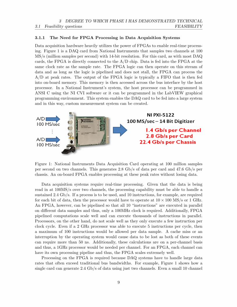
Data acquisition hardware heavily utilizes the power of FPGAs to enable real-time process-ing. Figure 1 is a DAQ card from National Instruments that samples two channels at 100MS/s (million samples per second) with 14-bit resolution. For this card, as with most DAQcards, the FPGA is directly connected to the A/D chip. Data is fed into the FPGA at thesame clock rate as the sample rate. The FPGA logic can then operate on this stream ofdata and as long as the logic is pipelined and does not stall, the FPGA can process theA/D at peak rates. The output of the FPGA logic is typically a FIFO that is then fedinto on-board memory. This memory is then accessed across the bus interface by the hostprocessor. In a National Instrument’s system, the host processor can be programmed inANSI C using the NI CVI software or it can be programmed in the LabVIEW graphicalprogramming environment. This system enables the DAQ card to be fed into a large systemand in this way, custom measurement system can be created.
Figure 1: National Instruments Data Acquisition Card operating at 100 million samplesper second on two channels. This generates 2.8 Gb/s of data per card and 47.6 Gb/s perchassis. An on-board FPGA enables processing at these peak rates without losing data.
Data acquisition systems require real-time processing. Given that the data is beingread in at 100MS/s over two channels, the processing capability must be able to handle asustained 2.4 Gb/s. If a process is to be used, and 10 instructions, for example, are requiredfor each bit of data, then the processor would have to operate at 10× 100 MS/s or 1 GHz.An FPGA, however, can be pipelined so that all 10 “instructions” are executed in parallelon different data samples and thus, only a 100MHz clock is required. Additionally, FPGApipelined computations scale well and can execute thousands of instructions in parallel.Processors, on the other hand, do not scale well as they only execute a few instruction perclock cycle. Even if a 2 GHz processor was able to execute 5 instructions per cycle, thena maximum of 100 instructions would be allowed per data sample. A cache miss or aninterruption by the operating system would cause data to be lost as both of these eventscan require more than 50 ns. Additionally, these calculations are on a per-channel basisand thus, a 1GHz processor would be needed per channel. For an FPGA, each channel canhave its own processing pipeline and thus, the FPGA scales extremely well.
Processing on the FPGA is required because DAQ systems have to handle large datarates that often exceed traditional bus bandwidths. For example, Figure 1 shows how asingle card can generate 2.4 Gb/s of data using just two channels. Even a small 10 channel
9

3.2 The FPGA Design Problem3 DEGREE TO WHICH PHASE I HAS DEMONSTRATED TECHNICAL
FEASIBILITY
system generates 14Gb/s of data traffic. This is more than a traditional PCI bus can handle.Since Compact PCI and PXI are all based on PCI, this is problematic. For high-end bustechnology, such as 32-lane PCI Express (PCIe), the data capacity is expanded to 64 Gb/s.Even this bandwidth is exhausted when 64 channels are utilized as this would require nearly90Gb/s of sustained throughput. It is clearly imperative that processing be performed bythe FPGA on the DAQ card itself.
3.2 The FPGA Design Problem
The problem, however, is that the traditional FPGA design flow is not well suited toscientists. Scientists are gifted individuals who have great depth in their domain of expertiseand utilize custom software in their experiments. Unfortunately, the traditional FPGAdesign flow does not capitalize on this capability and requires that a hardware descriptionlanguage (e.g. VHDL and Verilog) be used to design the FPGA. VHDL and Verilog are notjust another syntax for creating sequential programs but are low-level circuit descriptionlanguages that require the designer to have a detailed understanding of parallel logic design.Additionally, these languages are technology dependent and have to be rewritten for eachnew FPGA device. For example, the code for a 100MHz FPGA does not work well fora newer 200 MHz FPGA as the technology changes and new hardware resources, such asmultiply-accumulate blocks, are available to the designer. To achieve peak FPGA processingrates, as is needed by DAQ systems, the designers must exploit all of the available resourcesin the FPGA.
FPGA designs are complex and are labor intensive. In 2005, EE Times performed astudy of the design duration and costs associated with creating FPGA designs. As shownin Figure 2, only 9% of the designs were completed in 3 months, 17% in 3 to 6 months, and47% required 6 to 12 months. 27% required more than a year to complete. The mediandesign time was 9 months.
Figure 2: FPGA designs are both lengthy (9 months median length) and expensive ($360Kmedian cost), according to the 2005, EE Times FPGA Survey.
FPGA designs are also expensive. According to the same EE Times survey, the mediancost of an FPGA design was $360K. Almost half (48%) of the FPGA designs cost between
10
3.2 The FPGA Design Problem3 DEGREE TO WHICH PHASE I HAS DEMONSTRATED TECHNICAL
FEASIBILITY
$100K and $1M. 25% cost less than $100K and 23% cost over $1M.With 90,000 FPGA designs started each year, there is a significant market opportunity
if the design time and design costs can be significantly reduced.
3.2.1 Why are FPGAs so difficult to design?
At the core of the problem is the level at which designers are forced to work. An FPGAdesigner had to determine how much logic can be placed between every pair of registerssuch that the delay through this logic does not slow down the entire circuit. If a designincorrectly designs a single set of logic, the entire design must be slowed down. SinceFPGAs have a single clock, a single error in the design causes the entire FPGA to performslowly. This process is tedious and error prone.
Verification is also a lengthy portion of the FPGA design process. Typically, the domainexpert writes software to implement their algorithms. The design engineer then learns thealgorithm and manually converts the functionality of the software into parallel hardware.This requires that the design engineer have a detailed understanding of the algorithm.Verifying that the parallel hardware performs the exact same computation as the softwareis difficult as they were written in two entirely different languages with different designtools/compilers.
3.2.2 The Solution: The DAQ Accelerator Design Tool
As part of Phase I of this project, Concurrent EDA has customized their tools to dra-matically improve the speed of FPGA design for DAQ signal processing. This new toolis called the DAQ Accelerator as it enables software to be transformed into hardwarecomputations in an FPGA-based data acquisition card. Rather than requiring hardwareengineers to design at the logic-level, the DAQ Accelerator enables physics domain expertsto program the DAQ card using standard C software. The DAQ Accelerator enables thephysicist to view the FPGA DAQ hardware as a software function that is executed on everyA/D sample. A history of prior samples is also provided to the user so that they can viewup to 64 points on the analog waveform per sample.
Figure 3 shows the hardware framework for the DAQ Accelerator. In this diagram, theA/D chip is directly connected to the FPGA with its output labeled as A/D Samples. Aseries of registers within the FPGA buffer samples of the A/D to enable the user to accessprior samples. The user sees all A/D samples as an array called DAC[], where DAC[t] is theA/D sample from t cycles ago. Free running counters are also available to enable the user tochange the sampling rate or for timing calculations. The output of the logic is two signals,Valid and Result. If Valid is 1, then Result is placed into the FIFO, otherwise the currentsample (DAC[0]) is not kept. The data from the FIFO is sent to the host processor forfurther processing. In Phase I, we demonstrated that this process can be fully integratedinto the National Instruments DAQ FPGA hardware and integrated into the LabVIEWhost software.
The code in Figure 4 shows how samples that are close to zero are detected and ignored.Figure 5 is slightly more complex as it also incorporates a value from the knob on theLabVIEW console. This example demonstrates that configuration data from LabVIEW canbe sent into the FPGA to configure the user-specified computation. From a programming
11

3.2 The FPGA Design Problem3 DEGREE TO WHICH PHASE I HAS DEMONSTRATED TECHNICAL
FEASIBILITY
Figure 3: Concurrent EDA’s DAQ Accelerator Hardware Framework. This diagram showshow samples from the A/D are fed into the User Programmable FPGA Logic. The out ofthe User Logic is fed into a FIFO that interfaces with the DAQ Hardware.
perspective, these values are seen as a set of 32 global variables called WRITE_REG0 throughWRITE_REG31. Addition READ_REG values are also available to the user and are then availablewithin LabVIEW as a scalar value.
Concurrent EDA’s DAQ Accelerator is focused on enabling non-computer engineers tocreate high performance DAQ hardware. This tool is focused on scientists, who have thebest knowledge of the experiments but don’t want to design circuits just to conduct anexperiment. However, the quality of the results must not suffer and the automaticallygenerated circuits must be able to keep up with the A/D data rates. The user interface isthe same as that of a software compiler except that the final step requires an FPGA place-and-route run, which can take hours. To enable this last lengthy step to be performedonly once, DAQ Accelerator provides early area estimates for the user. As such, the usercan explore multiple algorithms quickly and selectively determine which ones need to bedownloaded onto the FPGA. See the DAQ Accelerator workflow detailed in Figure 6
3.2.3 How is this possible?
Compiled software is a sequence of simple processor instructions that perform operationson data stored in a set of software registers. If one instruction performs a computationand places the results in register R1 and another instruction reads R1, then there is a datadependency between the instructions. By creating a graph of these low-level instructionsand data dependencies, the computation can be unrolled and turned into hardware. Controlflow (e.g. if-then statements) can be turned into data flow through a process called predicted
12

3.2 The FPGA Design Problem3 DEGREE TO WHICH PHASE I HAS DEMONSTRATED TECHNICAL
FEASIBILITY
Figure 4: Concurrent EDA’s DAQ Accelerator enables signal processing software to beconverted into FPGA hardware designs in hours rather than months.
Figure 5: Demonstration of a Zero Suppression algorithm running on the FPGA in a Na-tional Instrument’s DAQ card and displayed in LabVIEW on the host processor. In thisexample, the knob changes the height of the “zero” band.
13

3.2 The FPGA Design Problem3 DEGREE TO WHICH PHASE I HAS DEMONSTRATED TECHNICAL
FEASIBILITY
Figure 6: Concurrent EDA’s DAQ Accelerator transforms user-defined software functionsinto a low-level data flow graph of operations. The graph above is the data flow graphof the zero-suppression program shown earlier. Using static timing analysis, this graph isconverted into FPGA logic and converted into an FPGA bit-stream.
14

3.3 Timing-related examples3 DEGREE TO WHICH PHASE I HAS DEMONSTRATED TECHNICAL
FEASIBILITY
execution. In this way, an entire function can be converted into a data flow graph. Sincewe are targeting DAQ hardware, the inputs and outputs are already defined. The graph isthen converted into a hardware data flow graph and operation-level timing information isincorporated into the graph. Static timing analysis is performed on this graph and registersare inserted to achieve the user-specified A/D sampling rate. The graph is then used tocreate VHDL that is then transformed into an FPGA bit-stream using the Xilinx (or Altera)backend tools.
3.2.4 What are the limitations of this approach?
There are no programming language restrictions within the DAQ_func() function. However,FPGA area is not unlimited and can be exhausted. Loops are allowed and are unrolledto create a pipelined hardware block. Large loops will require a large amount of FPGAhardware and may exceed the area available in the FPGA. Complex control flow commands,such as nested if-then-else structures and case/switch structures are allowed and can be ascomplex as needed. Both integer and floating point computations are allowed but requiredifferent amounts of FPGA area.
There are some function-level features that are available in software that do not work inversion 1.0 of the DAQ Accelerator tool. Recursive calls from DAQ_func() to itself are notallowed. However, fixed depth recursion can be converted in theory and may be includedas a feature later. Since this is not required and since the user has access to a large array ofprior A/D samples to implement recursive-like calls, this is currently a low priority feature.Function calls from within DAQ_func() to other functions is currently supported using the#inline command in the software. Future version will enable this automatically. Supportfor precompiled libraries is a feature that will be implemented in Phase II.
3.3 Timing-related examples
For various timing benchmarks, Landau shaped pulses were used. See Figure 7 for anexample Landau shaped pulse.
3.3.1 Leading edge discriminator
One of the simplest methods for extracting timing information from a detector pulse is athreshold discriminator followed by a TDC. This example approximates this functionalityof the threshhold discriminator using a high-speed ADC and FPGA. The basic premise isto analyze streaming input samples from the ADC and generate a timing signal when thesampled waveform value exceeds a set threshold.
3.3.2 Constant fraction discriminator
A more interesting tool for extracting timing information is a constant fraction discrimina-tor. A CFD offers significanly better timing resolution than a leading edge discriminatorbecause it addresses the issue of time-walk. Walk in this sense is a systematic shift in thetiming pulse related to the amplitude of the input pulse. A CFD addresses this problem bytriggering when a pulse is a certain fraction of its maximum amplitude.
15

3.3 Timing-related examples3 DEGREE TO WHICH PHASE I HAS DEMONSTRATED TECHNICAL
FEASIBILITY
Time0 50 100 150 200 250 300 350 400
Valu
e
-1800
-1600
-1400
-1200
-1000
-800
-600
-400
-200
0
200
Landau peak with gaussian noise
Figure 7: Simulated Landau pulse with Gaussian noise added.
Time0 200 400 600 800 1000 1200 1400 1600 1800 2000
Valu
e
-7000
-6000
-5000
-4000
-3000
-2000
-1000
0
Input samples
Time0 200 400 600 800 1000 1200 1400 1600 1800 2000
Valu
e
0
0.2
0.4
0.6
0.8
1
Output samples
Figure 8: Simulated Landau pulses as input with output timing pulses generated by aleading edge discriminator.
16

3.4 Digital pulse shaping examples3 DEGREE TO WHICH PHASE I HAS DEMONSTRATED TECHNICAL
FEASIBILITY
COTS hardware-based CFDs tend to be expensive in price, power consumption, andrack space (e.g. Ortec NIM module [7]). The performance of an FPGA-based CFD imple-mentation will of course be limited by ADC sample-rates, so this should be considered whenmaking direct comparisons between this example and dedicated hardware implementations.
This software implementation of a CFD is similar to the method used in an analoghardware based CFD. A key requirement for a CFD is that the rise-time of the inputpulses must be known. An input waveform is inverted and delayed (by the rise-time) beforebeing added to an attenuated (by a factor of 4) version of the original input waveform.These operations generate a bipolar waveform with a zero crossing at the time the originalpulse reaches 25% of maximum.
Time0 200 400 600 800 1000 1200 1400 1600 1800 2000
Valu
e
-7000
-6000
-5000
-4000
-3000
-2000
-1000
0
Input samples
Time0 200 400 600 800 1000 1200 1400 1600 1800 2000
Valu
e
0
0.2
0.4
0.6
0.8
1
Output samples
Figure 9: Simulated Landau pulses as input with output timing pulses generated by aconstant fraction discriminator.
Comparison of time walk for constant fraction and leading edge discriminatorsA large number of pulses with varied heights were analyzed using both leading edge andconstant fraction discriminators. Time walk is histogrammed in Figure 10 and Figure 11for each type of timing discriminator. The symbol, TMPV, in the time walk figures is thetime corresponding to the peak of the generated Landau pulse.
3.4 Digital pulse shaping examples
Analysis of electrical pulses is of critical importance to the extraction of valuable informationfrom many types of detectors. Digital pulse shaping is a type of digital pulse analysis thatis optimized for streaming processing of waveforms. Many analog filtering techniques canbe applied in the digital realm to sampled waveforms. The two following pulse shaping
17

3.4 Digital pulse shaping examples3 DEGREE TO WHICH PHASE I HAS DEMONSTRATED TECHNICAL
FEASIBILITY
[sample cycles]MPV - Tout T-20 -15 -10 -5 0 5 10 15 20
Co
un
ts
0
500
1000
1500
2000
2500
3000
3500
4000
Leading-edge discriminator walk time Entries 10000
Mean -10.56
RMS 1.099
Underflow 0
Overflow 0
Leading-edge discriminator walk time
Figure 10: Systematically reduced timing resolution from a leading edge discriminator.
[sample cycles]MPV - Tout T-20 -15 -10 -5 0 5 10 15 20
Co
un
ts
0
2000
4000
6000
8000
10000
Constant-fraction discriminator walk time Entries 10000
Mean 2
RMS 0
Underflow 0
Overflow 0
Constant-fraction discriminator walk time
Figure 11: Single ADC clock-cycle precision timing resolution from a constant fractiondiscriminator.
18

3.4 Digital pulse shaping examples3 DEGREE TO WHICH PHASE I HAS DEMONSTRATED TECHNICAL
FEASIBILITY
examples are used in spectroscopy systems (e.g. gamma ray). As it is more and morefeasible to put ADCs on every channel and process digital samples on front-end FPGAs,similar techniques become interesting for other detector applications.
3.4.1 Trapezoidal pulse shaper for exponential pulses
This pulse shaping example is an implementation of an algorithm given in Reference [8].The trapezoidal pulse shaper has the effect of generating a trapezoid (or triangular) pulsefrom an input exponential pulse.
In Figure Figure 12 the input pulse was the exponential (black) curve and the outputof the FPGA pulse shaping algorithm is the trapezoidal (red) pulse. The code for this isvery short and can easily process 100 MS/sec without losing any of the samples. A morerealistic case would involve noise being present in the signal. In Figure Figure 13 the sameshaping is applied with a noisy exponential input pulse. The zero line here has been raisedso that the baseline noise can be seen. It is clearly seen in this figure that the noise in theoutput trapezoidal pulse is significantly smaller than the noise in the input pulse. Thusnot only is it easy to produce a pulse of different shape than the input pulse, but it is alsotrivial to reduce noise in the pulse at the same time.
Time290 300 310 320 330 340 350 360 370 380
Valu
e
0
500
1000
1500
2000
2500
3000
Input
OutputTrapezoidal pulse shaper
Figure 12: Simulated sampled exponential pulse and result after application of the digitaltrapezoidal shaper.
The same basic principles are shown in producing a cusp-like pulse as shown in FiguresFigure 14 and Figure 15. The cusp-like filter is also an implementation of an algorithmpresented in Reference [8]. The second case once again adds noise to the exponential inputpulse, clearly showing the reduction in noise while outputting a pulse shape of whatever
19

3.5 Principal component analysis3 DEGREE TO WHICH PHASE I HAS DEMONSTRATED TECHNICAL
FEASIBILITY
Time290 300 310 320 330 340 350 360 370 380
Valu
e
0
500
1000
1500
2000
2500
3000
Input
OutputTrapezoidal pulse shaper
Figure 13: Simulated sampled exponential pulse with noise added and result after applica-tion of the digital trapezoidal shaper.
type is needed. These are fairly simple examples, but they demonstrate that digital pulseshaping FPGA code can be produced efficiently and flexibly.
3.5 Principal component analysis
Component analysis techniques are generally used to reduce high-dimensional data to lower-dimensional representations. Principal component analysis (PCA) is a linear method to ac-complish this task. In a physical system, PCA can often be used to extract dimensions thatare most significant physically (i.e. separating interesting signals from noise or combiningredundant measurements).
During Phase I, an example PCA was developed based on candidate tracks in a simplifiedversion of the Fermilab E906 di-muon spectrometer. Geant4 was used to simulate particletracks through the detector system. Figure 16 shows the detector geometry and simulatedtracks. The basic premise of this example is the common generic PCA process might beused as a pre-processing filter in part of an advanced FPGA accelerated trigger system.
Since the plan for Phase II is to work with Fermilab E906 this process was tested ontaking measurements made at x-y hodoscope planes to assess the ability to find tracks inreal-time. In this test six x-y planes were used, for a total of twelve measurements. E906will likely only have four x-y planes, but it was decided to increase the number of planes tobetter demonstrate the performance of the method. The basic layout of E906 is shown inFigure 16, which is a two-magnet spectrometer. This experiment is a followup experimentto Fermilab E866/NuSea, which determined the ratio of anti-down to anti-up quarks over anapproximate Bjorken x range of 0.05 to 0.25 via the Drell-Yan process. The DY process is
20

3.5 Principal component analysis3 DEGREE TO WHICH PHASE I HAS DEMONSTRATED TECHNICAL
FEASIBILITY
Time290 300 310 320 330 340 350 360 370 380
Valu
e
0
500
1000
1500
2000
2500
3000
Input
OutputCusp-like pulse shaper
Figure 14: Simulated sampled exponential pulse and result after application of the digitalcusp-like shaper.
Time290 300 310 320 330 340 350 360 370 380
Valu
e
0
500
1000
1500
2000
2500
3000
Input
OutputCusp-like pulse shaper
Figure 15: Simulated sampled exponential pulse with noise and result after application ofthe digital cusp-like shaper.
21

3.5 Principal component analysis3 DEGREE TO WHICH PHASE I HAS DEMONSTRATED TECHNICAL
FEASIBILITY
Magnet1 Magnet2
Target
x0,y0 x1,y1 x2,y2
x3,y3 x4,y4 x5,y5
DetectorStation
DetectorStation
DetectorStation
Detector Stationsand Absorbers
Figure 16: Simplified E906 di-muon spectrometer geometry from Geant4 simulation. Thepositive muon track is colored blue. Negative particle tracks (negative muon and ionizationelectrons) are colored red. For simplicity, this simulation assumes x-y coordinates will berecorded at all six detector planes, while the actual experiment has some y-only planes.The length of the apparatus is approximately 26 meters.
when a quark in the beam proton annihilates an anti-quark in the target proton or neutronsea, producing a virtual photon which then decays into a pair of leptons. The easiest ofcourse to detect is a di-muon pair due to high energy muons ability to penetrate materialused to absorb hadrons. E906 will extend the Nu/Sea measurements up to an x of around0.5.
Figure 17 shows the distribution of input data for the PCA. These data hit coordinatesat detector planes valid simulated positive muon tracks. Figure 18 shows the same datasetafter it has been transformed into the PCA coordinate space. The signifcant coordinates inthis case (pc0, pc1, pc2) correspond to a scaled linear combination of each muon’s initialmomentum vector. The outliers in the higher coordinates of Figure 18 correspond to muonsthat have undergone significant multiple scattering.
Invalid tracks (not shown) would tend to be very large in the higher PCA transformedcoordinates, while valid tracks would be generally very small in the higher PCA transformedcoordinates. This information could be used as the basis for a naïve track classifier, or itcould be combined with other data or more complicated techniques (e.g. artificial neuralnetworks) to create a powerful track classifier.
The reason this result is extremely interesting is that one could perform a PCA oninput data from a detector to determine if a particle track is present. Because of theparallel nature of the FPGA and its inherent pipeline structure, one gets a PCA resulton every clock cycle. This makes it possible to consider implementing a PCA hardwaretrigger, which would allow one to check for possible tracks while throwing none of the dataaway. One of the goals of working on FPGAs for the trigger hodoscopes for E906 to testthis methodology is to produce a trigger with zero dead time. This would mean that whiledoing a higher level track reconstruction process, as compared to a set of lookup matrices,no data are lost if the event being processed turns out to either have no tracks or has toomany tracks to successfully reconstruct. In the case of E906 the problem appears to be verydoable since the experiment is looking for di-muon pairs from Drell-Yan interactions. Thissimplifies the type of events one wants to record significantly, so Innovation Partners willwork with the E906 collaboration to produce the desired FPGA code for the trigger to runon FPGA boards based on designs already existing for other parts of the E906 detector. ThePrincipal Investigator has already worked in close contact with Pat McGaughey of LANL
22

3.5 Principal component analysis3 DEGREE TO WHICH PHASE I HAS DEMONSTRATED TECHNICAL
FEASIBILITY
Figure 17: Parallel coordinate diagram showing the distribution of input x and y coordi-nates in the laboratory coordinate system for valid positive muon tracks. These values aremeasured in inches at each detector plane.
23

3.5 Principal component analysis3 DEGREE TO WHICH PHASE I HAS DEMONSTRATED TECHNICAL
FEASIBILITY
Figure 18: Parallel coordinate diagram showing the distribution of valid positive muontracks that have been transformed into the principal coordinate space. The high ordercoordinates (pc9, pc10, pc11) are almost negligible for most valid tracks as most physicalinformation is in the lowest three coordinates (pc0, pc1, pc2).
24