implementation of low power active …eprints.usm.my/39556/1/raj_kumar_krishnasamy_24_pages.pdfthe...
TRANSCRIPT

IMPLEMENTATION OF LOW POWER ACTIVE
SECURITY MESH
By
RAJ KUMAR KRISHNASAMY
A Dissertation submitted for partial fulfilment of the
requirement for the degree of Master of Science
JUN 2017

ii
Acknowledgement
The dissertation has been made possible with the guidance and supervision of Dr. Khoo
Bee Ee. She kept in touch constantly to monitor the progress of the thesis and gave very
good ideas that shaped the dissertation.
I need to extend my appreciations to Jeff Khoo and Ong Chin Hu for their understanding
and support during the course of the dissertation.
Finally, to my wife and family who stood by me and encouraged me all the way.

iii
Table of Contents
Acknowledgement ............................................................................................................. ii
Table of Contents .............................................................................................................. iii
List of Tables ................................................................................................................... vii
List of Figures and Illustrations ...................................................................................... viii
List of Abbreviations and Nomenclature .......................................................................... xi
Abstrak ............................................................................................................................. xii
Abstract ........................................................................................................................... xiii
CHAPTER 1 ................................................................................................................ 1
INTRODUCTION ....................................................................................................... 1
1.1 Overview ............................................................................................................ 1
1.2 Challenges to IC industry................................................................................... 3
1.3 Problem Statement ............................................................................................. 6
1.4 Aim and Objective ............................................................................................. 6
1.5 Scope .................................................................................................................. 6
1.6 Thesis Outline .................................................................................................... 7

iv
CHAPTER 2 ................................................................................................................ 8
LITERATURE REVIEW ............................................................................................ 8
2.1 Overview ............................................................................................................ 8
2.2 Current Methods of attack ................................................................................ 8
2.2.1 Hack Attack ............................................................................................... 9
2.2.2 Shack Attack .............................................................................................. 9
2.2.3 Lab Attack ............................................................................................... 10
2.2.4 Fab Attack................................................................................................ 10
2.3 Evolution of mesh ............................................................................................ 11
2.4 Security Mesh .................................................................................................. 13
2.4.1 Passive mesh ............................................................................................ 13
2.4.2 Active mesh ............................................................................................. 14
2.5 Dense Random Spaghetti Active Shield .......................................................... 15
2.6 Other types of counter measures ...................................................................... 16
2.7 Methods and Tools ........................................................................................... 18
2.7.1 Focused Ion Beam ................................................................................. 18
2.7.2 Scanning Electron Microscope ............................................................. 20
2.7.3 Low cost probing station ....................................................................... 22
2.7.4 Probe Tips ............................................................................................. 23
2.7.5 Back Probing ......................................................................................... 24

v
CHAPTER 3 .............................................................................................................. 26
METHODOLOGY .................................................................................................... 26
3.1 Overview .......................................................................................................... 26
3.2 Implementation of active security mesh hard macros ...................................... 27
3.2.1 Linear Function Shift Register ................................................................. 28
3.2.2 Pseudorandom Bit Generator ................................................................... 29
3.2.3 Bit Comparator......................................................................................... 31
3.2.4 Initial seeds .............................................................................................. 33
3.3 Mesh wires ....................................................................................................... 34
3.3.1 How to choose the right metal layer for active mesh ............................... 35
3.3.2 Other factors to consider .......................................................................... 38
3.4 Active security mesh implementation .............................................................. 40
3.5 How to reduce the power consumption ........................................................... 43
3.5.1 Lower frequency ...................................................................................... 43
3.5.2 Optimization of the number of registers .................................................. 44
3.5.3 Inverter Block .......................................................................................... 44
3.5.3 Approach A .............................................................................................. 45
3.5.4 Approach B .............................................................................................. 48
3.6 Spice Simulation .............................................................................................. 50
3.6.1 What is a spice simulation ....................................................................... 50
3.6.2 How the spice simulation was created .................................................... 51
3.6.3 Calculating the power consumption......................................................... 53
3.6.4 Estimation using Power Analysis Tool .................................................... 54

vi
CHAPTER 4 .............................................................................................................. 56
RESULTS AND DISCUSSION ................................................................................ 56
4.1 Overview .......................................................................................................... 56
4.2 Testing the active mesh .................................................................................... 57
4.3 Power saving on active mesh ........................................................................... 60
4.4 Full chip power calculation .............................................................................. 61
4.5 Area used by the mesh ..................................................................................... 63
CHAPTER 5 .............................................................................................................. 66
CONCLUSION .......................................................................................................... 66
5.1 General ............................................................................................................. 66
5.2 Limitations ....................................................................................................... 67
5.3 Future improvements ....................................................................................... 68
REFERENCES ................................................................................................................ 70

vii
List of Tables
Table 1-1 Top 5 most counterfeited semiconductors in 2011 ...................................... 5
Table 2-1 Types of attack and its characteristics ....................................................... 11
Table 2-2 Hamilton Algorithm .................................................................................. 15
Table 4-1 Approach A power savings compare to original design ............................ 60
Table 4-2 Active mesh without any register optimization ......................................... 63
Table 4-3 Active mesh with Approach A .................................................................. 63
Table 4-4 Gate area of the active mesh ...................................................................... 64

viii
List of Figures and Illustrations
Figure 1-1 Trojan Horse ............................................................................................... 3
Figure 1-2 Hacked satellite decoder card ..................................................................... 4
Figure 1-3 Reports of counterfeit ................................................................................. 5
Figure 2-1 Classification of attacks ............................................................................. 8
Figure 2-2 Exposed bus lines ..................................................................................... 12
Figure 2-3 Etched power mesh .................................................................................. 12
Figure 2-4 Example of probing .................................................................................. 13
Figure 2-5 Example of active mesh ........................................................................... 14
Figure 2-6 Example of active mesh structures ........................................................... 14
Figure 2-7 DRSAS ..................................................................................................... 15
Figure 2-8 Example of data bus scrambling .............................................................. 16
Figure 2-9 MCU 6805 core has the data bus in order ................................................ 16
Figure 2-10 MCU 6805 core has the data bus scrambled .......................................... 17
Figure 2-11 Example of FIB station .......................................................................... 18
Figure 2-12 FIB edits ................................................................................................. 19
Figure 2-13 Physical IC Debug .................................................................................. 19
Figure 2-14 Reverse Engineering of a chip and standard cell ................................... 20
Figure 2-15 Image of mesh after the glass is etched away under SEM ..................... 21
Figure 2-16 Layers being overlaid using Photoshop ................................................. 21
Figure 2-17 Epoxy dissolved in hot nitric acid .......................................................... 22
Figure 2-18 Low cost probing station ........................................................................ 23
Figure 2-19 Probe tip ................................................................................................. 24
Figure 2-20 Back Side FIB ........................................................................................ 25
Figure 2-21 Camo cell ............................................................................................... 25

ix
Figure 3-1 Active Mesh Hard Macro ......................................................................... 27
Figure 3-2 Example of 8 bit LFSR with 3 taps .......................................................... 28
Figure 3-3 PBG behavioral code ................................................................................ 30
Figure 3-4 BC behavioral code .................................................................................. 32
Figure 3-5 Flawed placement ..................................................................................... 32
Figure 3-6 Serpentine shaped mesh wires can be bypassed using FIB ...................... 34
Figure 3-7 Serpentine shape nets can be easily mapped and bypassed ..................... 34
Figure 3-8 Mz layers are used to connect the power ................................................. 36
Figure 3-9 Security mesh nets are placed in between the Power and Ground ........... 39
Figure 3-10 Good example of mesh covered chip by My.......................................... 39
Figure 3-11 Mesh wires must cover the block pins ................................................... 39
Figure 3-12 Active security mesh hard macro placement.......................................... 40
Figure 3-13 Optimum placement for active security mesh hard macro ..................... 41
Figure 3-14 Active security mesh placement for large IP ......................................... 42
Figure 3-15 Added IB into BC ................................................................................... 45
Figure 3-16 Approach A uses half the registers ......................................................... 46
Figure 3-17 Approach A security features ................................................................. 47
Figure 3-18 Approach B ............................................................................................ 48
Figure 3-19 How mesh wires can be shorted ............................................................. 49
Figure 3-20 Example of spice run deck ..................................................................... 51
Figure 3-21 Example of the spice result .................................................................... 52
Figure 3-22 RedHawk dynamic power analysis flow ................................................ 55
Figure 3-23 Example of IR drop map ........................................................................ 55
Figure 4-1 Testing the active mesh on test bench ...................................................... 57
Figure 4-2 Alarm goes high when the mesh wires are tampered .............................. 58

x
Figure 4-3 Example of the testbench used ................................................................. 59
Figure 4-4 Power number comparison between spice simulation and RedHawk .... 61
Figure 4-5 Example of die size .................................................................................. 64
Figure 4-6 Different floorplan requirement ............................................................... 65

xi
List of Abbreviations and Nomenclature
Abbreviation Meaning
ATM Automated Teller Machine
BC Bit Comparator
CMP Chemical Mechanical Planarization
DIP Dual Inline Package
DRC Design Rule Check
DRSAS Dense Random Spaghetti Active Shield
FIB Focused Ion Beam
GDS Graphic Database System
HM Hard Macro
IB Inverter Block
IC Integrated Circuit
LB Litar Bersepadu
LFSR Linear Function Shift Register
LKAC Litar Keselamatan Anti-Ceroboh
LMC Laser Micro Chemical
Mx Metal in the lower stack, has higher resistance
My Metal in the middle stack, has lower resistance than Mx layers
Mz Metal in the highest stack, has lowest resistance
PBG Pseudorandom Bit generator
PVT Process, voltage, temperature
RDL Redistribution Layer
RE Reverse Engineering
SEM Scanning Electron Microscope
TV Television
JTAG Joint Test Action Group
BIST Built-In Self-Test
xii
Implementasi Litar Keselamatan Anti-Ceroboh Berkuasa Rendah
Abstrak
Keselamatan Litar Bersepadu(LB) merupakan isu besar kepada banyak syarikat korporat
kerana banyak peranti tiruan telah wujud di pasaran. Banyak langkah keselamatan telah
diambil untuk mengatasi masalah ini seperti litar keselamatan anti ceroboh(LKAC), litar
cegah gangguan voltan dan penyulitan data. Kebanyakan LB hanya beroperasi pada satu
frekuensi sahaja. Ini sangat merugikan kuasa apabila LB tidak membuat apa-apa operasi.
Kajian ini bertujuan mereka LKAC yang mudah dan berkuasa rendah. Ia juga menguji
beberapa frekuensi untuk mendapatkan jumlah kuasa yang rendah. Jumlah kuasa
dibanding antara LKAC asal dan LKAC baru. LKAC baru menggunakan peranti logik
yang optimum dan beroperasi pada frekuensi yang lebih rendah. Kuasa akan dikira
menggunakan anggaran “spice”. Kajian berikutnya membandingkan jumlah kuasa yang
digunakan oleh LKAC yang baru melalui Spice dan melalui perisian penganalisa kuasa
seperti RedHawk. Tujuan kajian ini adalah untuk membuktikan penjimatan kuasa.
Berdasarkan kedua kajian di atas, boleh dirumuskan bahawa pengurangan peranti logik
dan kawalan frekuensi yang optimum boleh mengurangkan penggunaan kuasa sebanyak
96.6%. Nilai ini adalah satu anggaran yang pesimistik dan jumlah penjimatan adalah lebih
tinggi sebenarnya. Jadi, keselamatan LB boleh dijaga dan jumlah kuasa boleh dijimatkan
semasa LB tidak beroperasi.

xiii
Implementation of Low Power Active Security Mesh
Abstract
Integrated Chip (IC) security has been a big concern for companies and consumers as the
number of counterfeit devices have increased tremendously. Many counter-measures have
been taken to improve the chip security like anti-tamper mesh, glitch protection and
encryptions. The current anti tamper mesh usually runs on a single frequency and would
consume a lot of power when the chip is idle. An inefficient mesh implementation would
cause the die size to increase but the area protected would not be complete. This research
will concentrate to make the anti-tamper mesh simple and secure yet, consumes low
power. It uses the least resource in terms routing tracks and makes use of several operating
frequencies to get the best of power consumption. The power number is compared using
standard cell spice simulation numbers. The cells with reduced gate count and reduced
frequency are compared with original settings using spice simulation number. The second
experiment was done to compare the numbers from the spice simulations against power
analysis tool. This is to ensure the spice simulation numbers reflect the power saving and
to prove that the savings are real and can be even lower than estimated. Based on the
experiments, it can be concluded that varying the frequencies of the active security mesh
blocks and reduction of registers used can save power and still maintain the integrity of
the active mesh. The spice simulation numbers are pessimistic and in power analysis, it is
shown to be much lower. The total power saved by reducing the registers is 34.4%. When
the registers and frequency are reduced, the total savings is about 96.6%.

1
CHAPTER 1
INTRODUCTION
1.1 Overview
Integrated Chip (IC) are an integral part of our life in these modern days. The chips are
everywhere, in consumer devices, banking, entertainment, communications devices,
transportation and medical industry. The evolution of IC from several transistors in a
single chip to billion gates in processors just shows the importance of IC in everyday life.
According to Moore’s law, the density of gates would double every year driving down the
cost, size and doubling in performance. Even digital cameras have zoomed past its older
cousin, the exposure film, adding millions of pixels on its way to snatch the supremacy in
photography industry.
Healthcare industry is teeming with life as age boundary is pushed further, life expectancy
is higher than a century ago. More elderly people are actively participating in everyday
activities and contribute till much later part of their life. Many exoskeleton equipment and
life support devices have IC in them to do a million calculations and execute the right
movement in a short fraction of time.
Transportation is an industry that is very heavily dependent on IC to improve the safety
and reliability of the machines. It is no more a component that provides entertainment
videos or music but one that is heavily involved in braking, maneuvering and reducing the
impact of a collision in cars.

2
For example, air plane safety standards are so high and without IC, it would be impossible
to achieve it. Imagine a fighter jet without the advancement of IC technologies, it would
not be able to fly at high speed while keeping an eye on the target.
Banking industry have gone global, contributing to the economy to countries across the
globe. People can travel worldwide and conduct transaction everywhere. Automated
Teller Machine cards enable people to withdraw cash anytime convenient to them.
Security key fobs enable people to conduct electronic banking from the comfort of their
homes.
Communications have made the world smaller, with miles of fiber optics and array of
technology chips make data transfer safe and possible. Companies can safely transfer
company related data for business activities online.
IC have become extremely important in today’s world that almost everyone’s lives are
touched by the technology. With so much of importance in IC, imagine a scenario where
someone, a hacker, a data thief or corporate espionage decides to take the chip and clone
it and manufacture and sell the cloned chips at lower price. It would spell a death knell to
the original manufacturer.
Before 1995, the cards had no mesh, the data bus was not scrambled and the data was not
encrypted. Post 2000, passive mesh was introduced, data bus scrambling was introduced
and data encryption was also introduced. Post 2005, many new technologies were
introduced like implementing internal oscillator, active security mesh, encryption, bus
scrambling, glitch sensors, voltage monitors, camo cells and custom internal oscillators.

3
1.2 Challenges to IC industry
Corporate espionage can add a “Trojan horse” in the chip. Trojan horse in a chip means
the chip function will differ than the original design of the chip (Wang et al., 2008). It
could either be overwriting the security features of the chip, bypass the encryption or write
out crucial data from the chip.
Figure 1-1 Trojan Horse (Wang et al., 2008)
Data thief would probe the IC on an ATM card or satellite decoders and steal the keys
embedded in the card and use it to manufacture cloned cards. With the cards, the thief can
withdraw cash from the ATM or use the satellite channels for free (Olivier Thomas
BlackHat 2015). Both the actions would result in huge loss for the public and corporations.

4
Figure 1-2 Hacked satellite decoder card (Olivier Thomas BlackHat 2015)
The effects would be worst if medical devices are cloned for profit as it would result in
patients getting substandard or expired medical devices. Companies have invested
millions in research and development of the devices. A hacker can steal the information
on the chip and clone the product and sell it at lower cost. These activities are getting
bigger by the year as the amount of money involved is huge and the interest shown by
certain parties are encouraging.
The occurrence of counterfeit devices has been increasing at break neck pace lately and it
is expected to get worse. It has infiltrated global electronic supply chain as the cost of
counterfeit devices are lower. Hackers are improving their techniques making it very hard
to detect counterfeit devices. (The hacker is also known as data thief or attacker).
The effect of these developments is a main cause of worry to manufacturers and also to
consumers. Imagine a plane that is flying at high speed and the navigation system fails.
That would be a nightmare scenario for the pilots.

5
Table 1-1 Top 5 most counterfeited semiconductors in 2011
(IHS Parts Management 2012)
Ranks Component type
% of reported
incidents
1 Analog IC 25.2
2 Microprocessor IC 13.4
3 Memory IC 13.1
4
Programmable logic
IC 8.3
5 Transistors 7.6
The graph below shows the amount of counterfeit parts detected in global supply chain in
the last few years. Hackers would take a chip, break it down layer by layer and duplicate
the design and reproduce the chip at a fraction of the cost (Guin et al, 2014). For fabless
manufacturers, supply chain security is a great concern as they would need to comb for
genuine devices. Mass selling products like medical devices, consumer products like game
consoles are targeted due to the size of the market.
Figure 1-3 Reports of counterfeit (Guin et al., 2014)

6
1.3 Problem statement
Hackers are using advanced tools to read the memory and data bus on a chip. Therefore,
a good active mesh need to be designed to deter the hackers. Active security mesh uses a
significant amount of die area and in order to improve the effectiveness of the security
mesh, more than 1 metal layer need to be used. That would increase the cost of the chip.
Active security mesh need to be running at all time to give the best protection for the chip
it intends to protect. However, that would make the active security mesh unsuitable for
low powered devices like mobile devices.
1.4 Aim and Objective
The objective of the thesis is to create an active mesh system that
1) Has high security, simple implementation, low cost and uses minimum area
2) Consumes lower power during idle and runs at higher frequency to maximize the
protection for the chip
1.5 Scope
The scope of the research will be on the
1) design of active security blocks that utilizes minimum amount of area
2) design a mesh using single metal layer for both the mesh signals and power bus
3) design the active security mesh to use the lowest amount of power during idle
4) compare the power savings between spice simulation and power analysis

7
1.6 Thesis outline
There are 5 chapters that will be discussed in the thesis. By the end of the fifth chapter,
the thesis should be able to prove the need of active security mesh and how easy it is to
implement the mesh in a chip, what are the requirements and how to implement the mesh
in low power devices.
Chapter 1 discusses the problem security problem that many IC manufacturer faces and
the need for a low power active mesh.
Chapter 2 discusses about the current technologies that are available in the market. It
discusses about the technologies are used to delayer the chip and reverse engineering
Chapter 3 discusses on the design and the methodologies that will be applied to design the
active mesh
Chapter 4 will focus on the experiments done to implement the active mesh and the steps
to reduce the power consumption.
Chapter 5 concludes the thesis with results of the experiments and explanations. It also
includes future suggestion on how to make the chip more secure in the future.

8
CHAPTER 2
LITERATURE REVIEW
2.1 Overview
This chapter will discuss the current attack methods, types of metal mesh, evolution of
security mesh, the available counter measures and the technologies used to do physical
tampering. The latest trend in physical tampering is back side tampering. It will be
discussed at the end of the chapter.
2.2 Current methods of attack
Physical attacks can be categorized as Invasive Attacks, Non-Invasive Attacks and Semi-
Invasive Attacks.
Figure 2-1: Classification of attacks (Tehranipoor, Mohammad, (2012))

9
Table 2-1: Types of attack and its characteristics (Tehranipoor, Mohammad, (2012))
In some reports, the attacks are classified as Hack, Shack, Lab and Fab attack. It can be a
combination of direct physical attack, glitches, or through malware (Iqbal, 2013).
Although the classifications are different, the attacks are similar to Fig.2-1. For example,
Reverse Engineering is done in Lab Attack while Fault Injection is part of Shack Attack.
2.2.1 Hack Attack
The attacker executes viruses or malware into the device after initiating contact with the
device. The contact could be direct physical contact or by wireless protocol. Usually the
hacker would send a software claiming to be an update or add-on. When the user approves
the installation, the malware embedded in the software would be installed also.
2.2.2 Shack Attack
The attack, like its name, is a low-cost hardware attack. The hardware to execute the attack
can be bought from electronic hardware stores or online (Greg Wood, 2016). The attacker

10
would probe the signals, pins or busses using probes and network analyzers. The person
would use test features in the IC like BIST, JTAG and boundary scan to probe the
functional state. Usually the type of attack is quite simple like forcing the logic on the pins
like logic 1 or 0, reprogramming the memory devices or bypassing some components.
2.2.3 Lab Attack
This type of attack is done by a group who has modern equipment and lab facilities.
Usually will cost more and requires a higher expertise compare to hack and shack attack.
The attackers would be able to reverse engineer the logic and memory, glitch the signal
nets and scan the layout using electron microscope.
The attack on this scale would be able to perform cryptographic key analysis and analyze
analog signals. The attacker can bridge IC chip net traces using FIB to reroute data or pins.
2.2.4 Fab Attack
This is the lowest form of attack where the attacker edits the layout and add additional
monitor circuit into the layout. These edits are in GDS form and are done in foundry or
fabrication plant. The advantage of this edit is that the edits cannot be detected by regular
validation tools. It takes an experienced engineer to monitor the power or signal pattern
to know that an attack is going on.
Overbuilding happens when the fab produces more than ordered part and uses the extra
parts as counterfeits (Gedare Bloom et al, 2010). Stolen mask sets or the GDS database
are known as fab attack.

11
2.3 Evolution of mesh
Chip security has been a big concern for some time. In the entertainment industry, satellite
TV have huge customer pool and hackers see an opportunity to create and sell cloned
cards. They used a variety of low cost micro probing techniques to steal the information
from the cards. Shack attack, lab attack or invasive attack require micro probing into the
chip. A good protection is needed to protect the chip against micro probing.
Mesh wires are made of additional metal layer on top of the die. Initially it does not carry
any signal or clock nets. It just blocks the attacker from probing any of nets in the chip.
The attackers managed to find a way to etch the mesh and expose the nets underneath the
mesh wires.
Etching the mesh layers is not very straight forward as the thickness of the mesh layers
and glass oxide underneath the mesh would differ. Although chemical mechanical
planarization polishes the surface to be near perfect flat, it is not meant for the top layer
to be etched away. Once the top layer is etched using chemical process, the surface would
not be evenly etched. All these have changed with probing and imaging technology
advancement.
Passive security mesh was introduced later but it was later found that the mesh wires can
be altered without triggering the alarm.
Active security mesh overcame the problem that passive security mesh faced. It monitors
the mesh wires continuously for open or forced logics. The active meshes were
implemented in many products available in the market. Active mesh was first introduced

12
in ST series smartcards. However, design flaws in active mesh made the chip vulnerable
to attacks.
For example, ST16SF48A (Fig.2-2) chip has redundant extension of the bus that is not
protected by the mesh, making it easy to be probed. Another chip had mesh interleaved
with power and ground nets (Fig.2-3). The attacker simply removed a portion of the PG
nets using FIB.
Figure 2-2 Exposed bus lines Figure 2-3 Etched power mesh
13
2.4 Security mesh
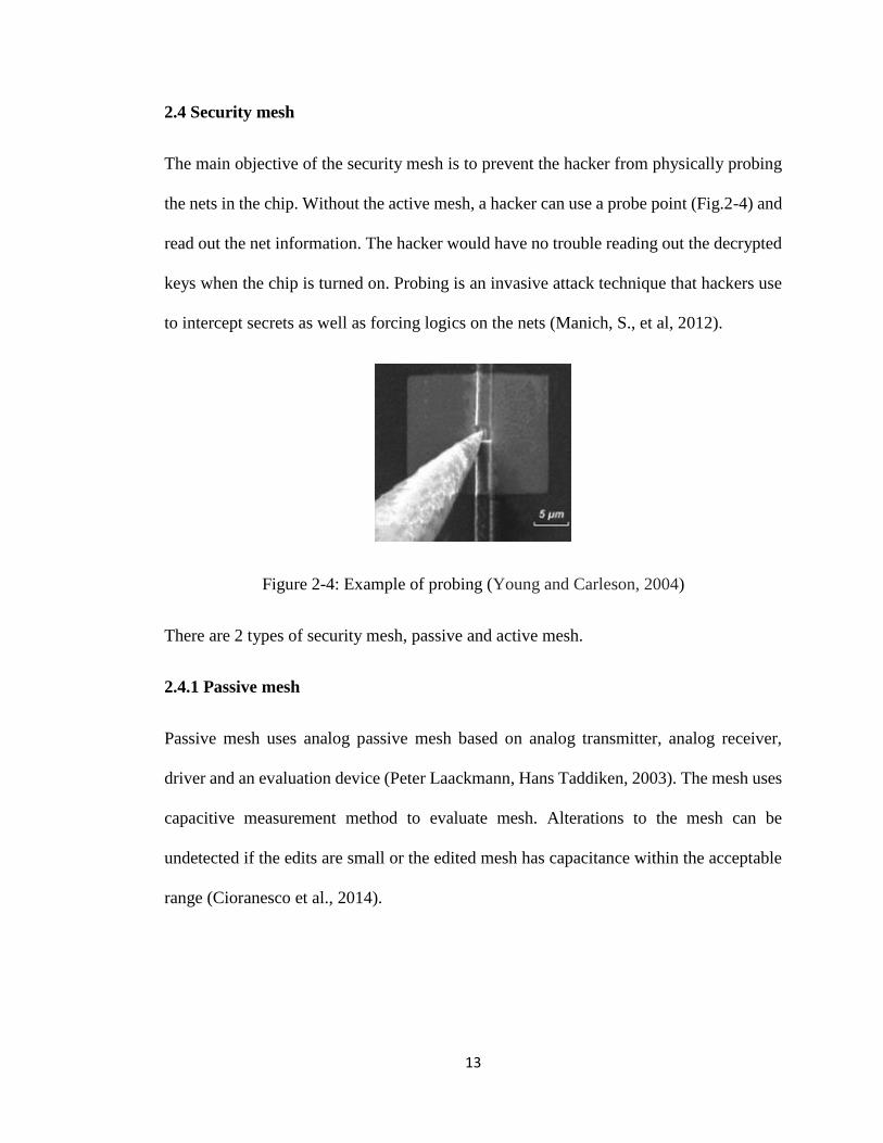
The main objective of the security mesh is to prevent the hacker from physically probing
the nets in the chip. Without the active mesh, a hacker can use a probe point (Fig.2-4) and
read out the net information. The hacker would have no trouble reading out the decrypted
keys when the chip is turned on. Probing is an invasive attack technique that hackers use
to intercept secrets as well as forcing logics on the nets (Manich, S., et al, 2012).
Figure 2-4: Example of probing (Young and Carleson, 2004)
There are 2 types of security mesh, passive and active mesh.
2.4.1 Passive mesh
Passive mesh uses analog passive mesh based on analog transmitter, analog receiver,
driver and an evaluation device (Peter Laackmann, Hans Taddiken, 2003). The mesh uses
capacitive measurement method to evaluate mesh. Alterations to the mesh can be
undetected if the edits are small or the edited mesh has capacitance within the acceptable
range (Cioranesco et al., 2014).

14
2.4.2 Active mesh
Passive mesh has a weakness that are exploited by hackers to remove the mesh layers.
Active mesh (Fig.2-5) consists in injecting random sequences of bits through the mesh
wires. The random signals are checked at the end of the mesh wires to check for any
differences. These are usually digital in nature and cannot be altered by the hackers using
external wires. The dissertation will discuss about active mesh.
Figure 2-5: Example of active mesh (Tarnovsky, 2010)
Active and passive mesh do not protect against delayering. However, they do protect
against dynamic attacks that occurs when the chip is rebooted or extraction of decrypted
key from non-volatile memory. This data cannot be retrieved when the chip is in off state.
Figure 2-6 Example of active mesh structures (Cioranesco et al., 2014)

15
2.5 Dense Random Spaghetti Active Shield (DRSAS)
The concept behind DRSAS (Briais, et al., 2012) is to use 2 metal layers (metal 5 and
metal6) and lay them in unpredictable pattern. The layout is so dense that there will be no
tracks missed by either one of the 2 metal layers. It is called Hamiltonian path.
The algorithm for Hamiltonian path is described below as Table 2-2. (As taken from
Briais, et al., 2012)
Input: N: number of different interleaved equipotentials
Output: A random shield made of N equipotentials
1: Build a graph whose vertices consists in free via slots and edges in the
free routing slots
2: Label each edge by a random number
3: Solve the Traveling Salesman Problem (TSP) to get one Hamiltonian
circuit
4: Cut the Hamiltonian circuit into N subpaths, and return those.
Table 2-2 Hamilton Algorithm
An example of DRSAS done using Table 2-2 is in Figure 2-7. This is quite an effective
mesh but it uses 2 metal layers and 1 via layers. Therefore, the cost is higher.
Figure 2-7 DRSAS

16
2.6 Other types of counter measures
Bus scrambling is a security technique that has been around since late 90s.
Figure 2-8 Example of data bus scrambling
The bus ordering in a chip is usually in order. For example, an 8 bit bus, the bus sequence
is as follows. mem_ports[7:0]=mem_bus[7,6,5,4,3,2,1,0].
Once the bus has been identified, the hacker can eavesdrop on the bus to read out the keys,
or the boot sequence.
Figure 2-9 MCU 6805 core has the data bus in order (Motorola SC27/28 Smartcard)
The data buses are scrambled to throw the hacker of in different direction. The person
would need to understand the chip design.
17
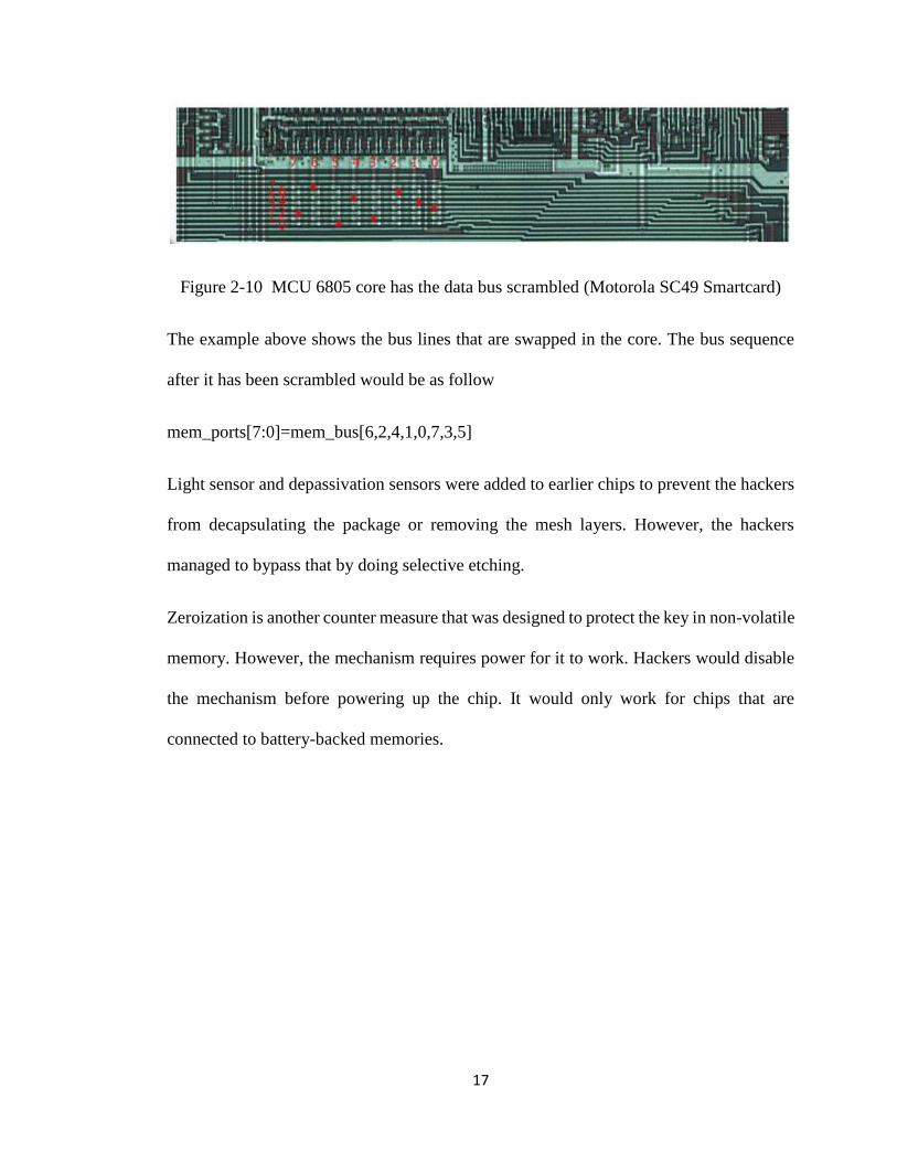
Figure 2-10 MCU 6805 core has the data bus scrambled (Motorola SC49 Smartcard)
The example above shows the bus lines that are swapped in the core. The bus sequence
after it has been scrambled would be as follow
mem_ports[7:0]=mem_bus[6,2,4,1,0,7,3,5]
Light sensor and depassivation sensors were added to earlier chips to prevent the hackers
from decapsulating the package or removing the mesh layers. However, the hackers
managed to bypass that by doing selective etching.
Zeroization is another counter measure that was designed to protect the key in non-volatile
memory. However, the mechanism requires power for it to work. Hackers would disable
the mechanism before powering up the chip. It would only work for chips that are
connected to battery-backed memories.

18
2.7 Methods and tools
2.7.1 Focused Ion Beam (FIB)
Figure 2-11 Example of FIB station (Image from
http://www.brucherseifer.com/html/sem___fib.html)
Focused Ion Beams or FIB, is a tool that performs chip level surgery. The concept behind
FIB is similar to SEM. FIB can be used for imaging, cut nets off and modifications to the
nets. It uses energized Ga+ ions.
FIB can image sample up to 5nm resolution. If the beam current is increased, FIB can be
used to cut the metal. Attackers use FIB to do manual probing of metals that are embedded

19
deep in the die or the poly nets (if probe from the back side of the die). Once the hole is
made to the net of interest, platinum will fill the hole to create a probe pad.
FIB can be used to modify layout on the die directly (Cole et al, 2009). This is very useful
for a design and test engineer as they can perform a quick modification on the die to see
if the edits can fix the chip failure (Fig.2-12). It is fairly quick to set up and use.
FIB workstations are very expensive to operate; therefore, most companies would rent the
workstations on hourly basis.
Figure 2-12: FIB edits (Cole et al., 2009)
However, FIB would be very costly for back side modifications. FIB requires an open
area to do the modifications, the deeper the net, the larger the open area.
Figure 2-13 Physical IC Debug (Boit et al., 2008)

20
2.7.2 Scanning Electron Microscope
The chip can be delayered one layer at a time. Once delayered, Scanning Electron
Microscope (SEM) are used to extract the image in high resolution. The images are fed
into software like Photoshop where the images can be stacked on one another to study the
chip. These technique is very useful in reverse engineering or understanding the mesh
patterns. Tarnovsky (2010) has demonstrated the method and he used Photoshop to
overlay the images.
Poly layer Metal1
Metal2 Metal3
Figure 2-14 Reverse Engineering of a chip and standard cell (Thomas, 2015)

21
Figure 2-15 Image of mesh after the glass is etched away under SEM
Figure 2-16 Layers being overlaid using Photoshop (Tarnovsky, 2010)

22
2.7.3 Low cost probing station
The cost of doing an invasive attack on an IC has come down and this plays a part in
increasing the number of counterfeit devices in the market.
Invasive attacks mean probing the signal or clock nets using a probe. In order to do this,
the chip package has to be removed and a decent probing station is required. Probing
stations are made up of microscopes and controllable arm that can maneuver the fine probe
or “cat whiskers” on the surface of the chip. Some has laser accessories to create a hole
on the passivation layers. Usually these types of probing stations can be found in
production line to do manual testing.
For package removal (in the case of epoxy package), the chip need to be dipped in nitric
acid that has been heated to 60°C until the black epoxy dissolves. The chip is then soaked
in ultrasonic acetone bath. If needed, wash the chip in deionized water and isopropanol.
Figure 2-17: Epoxy dissolved in hot nitric acid

23
Figure 2-18: Low cost probing station
2.7.4 Probe Tips
As the IC technology shrinks, the net width also shrinks. Attacker would need a very fine
probe tips to probe the nets. The tips are also called cat whisker. They have to use probe
pins that are smaller than the metal width size else they would end up shorting the net.
The technology behind the probe tips is quite impressive as some probe tip can be as small
as 0.1um radius. It is mainly made of tungsten.

24
Figure 2-19 Probe tip
2.7.5 Back Probing
As technology in scanning and FIB advances, hackers have found new creative ways to
tap into the die without touching the active mesh. Initially this technology was designed
to help with chip test and failure analysis. The alarm would not go off and the hacker
would be able to power up the chip to steal the data.
It was not very famous before as the hacker would not be able to FIB through the back
side of the IC without damaging the diffusion layers and the person would be trying in the
dark many times before he hits a correct clock or data bus. Moreover, the person would
be able to probe first few metal layers only as probing deeper would require bigger area
to FIB.
The preparation for back side probing require thinning of the silicon layer. This is usually
done by FIB or Laser MicroChemical (LMC) Etching (Barton et al., 2004). FIB is quite
accurate but costly. Figure 2-20 shows the attacker accesses the metal lines using backside
FIB.
Figure 2-20: Back Side FIB