implementation of combined svl technique in domino ... · overheads in terms of chip area and speed...
TRANSCRIPT
International Research Journal of Engineering and Technology (IRJET) e-ISSN: 2395-0056
Volume: 05 Issue: 12 | Dec 2018 www.irjet.net p-ISSN: 2395-0072
© 2018, IRJET | Impact Factor value: 7.211 | ISO 9001:2008 Certified Journal | Page 464
Implementation of Combined SVL Technique in Domino Inverter
using Microwind
K. Kalai Selvi
Assistant Professor, Dept. of Electronics & Communication Engineering, Government College of Engineering, Tirunelveli, India
---------------------------------------------------------------------***---------------------------------------------------------------------Abstract - This paper implements self controllable voltage level circuit in 2 levels -upper & lower levels & called combined self controllable voltage level circuit for power reduction in Domino circuit. Back gate bias is increased & Drain induced lowering effect is reduced by the circuit. This change increases threshold voltage which reduces leakage current. All the simulations have been carried out in Microwind tool at 90 nm technology ,Vdd Supply of 1.2 volt is given , input sequence used is 01010.The other name of Self controllable Voltage Level is Adaptive voltage level circuit (AVL).
Key Words: Static CMOS, Combined self controllable voltage level USVL, (upper self controllable voltage level) ,LSVL (lower self controllable voltage level), Leakage current, Power dissipation.
1. INTRODUCTION CMOS consists of both PMOS field effect transistors (FETs), which is suitable for efficiently driving a high voltage or logic one value, and NMOS transistors, which is good for a zero voltage. The presence of complementary transistors permits CMOS logic gates to be implemented so that the output voltage level is connected to the power or ground line, but not both. This ability to prevent contention ensures that if the inputs are not changing, then no power is dissipated. This was a benefit of CMOS over the others available, which dissipated constant leakage or bias currents. when the inputs to a CMOS circuit do not change, often called a standby or idle state, almost no power dissipation occurs, CMOS implementations reduced standby power by six orders of magnitude over equivalent bipolar and PMOS implementations except for a small leakage current which flows through the transistors due to the imperfect manner in which a MOSFET behaves as a switch (due to the persistent scaling in the physical dimensions of CMOS processes, driven by the cost advantages of having a smaller silicon area for digital functions, MOS transistors have become less efficient switches, leading to greater leakage current).
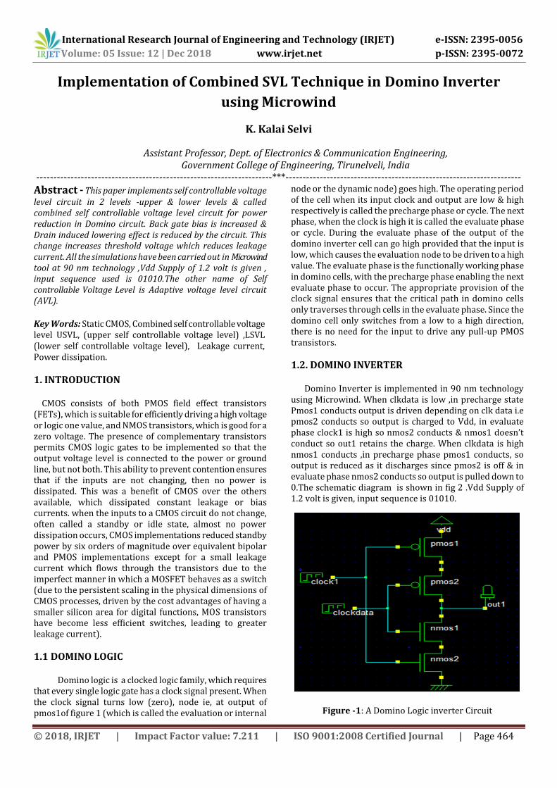
1.1 DOMINO LOGIC
Domino logic is a clocked logic family, which requires that every single logic gate has a clock signal present. When the clock signal turns low (zero), node ie, at output of pmos1of figure 1 (which is called the evaluation or internal
node or the dynamic node) goes high. The operating period of the cell when its input clock and output are low & high respectively is called the precharge phase or cycle. The next phase, when the clock is high it is called the evaluate phase or cycle. During the evaluate phase of the output of the domino inverter cell can go high provided that the input is low, which causes the evaluation node to be driven to a high value. The evaluate phase is the functionally working phase in domino cells, with the precharge phase enabling the next evaluate phase to occur. The appropriate provision of the clock signal ensures that the critical path in domino cells only traverses through cells in the evaluate phase. Since the domino cell only switches from a low to a high direction, there is no need for the input to drive any pull-up PMOS transistors.
1.2. DOMINO INVERTER
Domino Inverter is implemented in 90 nm technology using Microwind. When clkdata is low ,in precharge state Pmos1 conducts output is driven depending on clk data i.e pmos2 conducts so output is charged to Vdd, in evaluate phase clock1 is high so nmos2 conducts & nmos1 doesn’t conduct so out1 retains the charge. When clkdata is high nmos1 conducts ,in precharge phase pmos1 conducts, so output is reduced as it discharges since pmos2 is off & in evaluate phase nmos2 conducts so output is pulled down to 0.The schematic diagram is shown in fig 2 .Vdd Supply of 1.2 volt is given, input sequence is 01010.
Figure -1: A Domino Logic inverter Circuit
International Research Journal of Engineering and Technology (IRJET) e-ISSN: 2395-0056
Volume: 05 Issue: 12 | Dec 2018 www.irjet.net p-ISSN: 2395-0072
© 2018, IRJET | Impact Factor value: 7.211 | ISO 9001:2008 Certified Journal | Page 465
2. SELF CONTROLLABLE VOLTAGE LEVEL
SVL stands for Self controllable Voltage Level. A self-controllable voltage level (SVL) circuit can supply a maximum dc voltage to an active-load circuit on request or can decrease the dc voltage supplied to a load circuit in standby mode is developed.
This SVL circuit can drastically reduce standby leakage power of CMOS logic circuits with minimal overheads in terms of chip area and speed .SVL is a technique which can be set either at the top of the load, or bottom of the load or both.
2.1 Combined SELF CONTROLLABLE VOLTAGE LEVEL
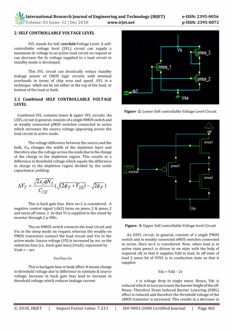
Combined SVL contains lower & upper SVL circuits .An LSVL circuit in general, consists of a single NMOS switch and m weakly connected pMOS switches connected in series which increases the source voltage appearing across the load circuit in active mode.
The voltage difference between the source and the bulk, VSB changes the width of the depletion layer and therefore also the voltage across the oxide due to the change of the charge in the depletion region. This results in a difference in threshold voltage which equals the difference in charge in the depletion region divided by the oxide capacitance, yielding:
This is back gate bias. Here m=2 is considered. A negative control signal (clk2) turns on pmos_3 & pmos_2 and turns off nmos_1. So that Vs is supplied to the stand-by inverter through 2 p-SWs.
The on-NMOS switch connects the load circuit and
Vss in the sleep mode on request whereas the weakly-on PMOS transistors connect the load circuit and Vss in the active mode. Source voltage (VS) is increased by mv, so the substrate bias (i.e., back-gate bias) (Vsub), expressed by Vsub = – mv
Vs=Vss+2v
This is backgate bias or body effect. It means change in threshold voltage due to difference in substate & source voltage. Increase in back gate bias lead to increase in threshold voltage which reduces leakage current
Figure -2: Lower Self controllable Voltage Level Circuit
Figure- 3: Upper Self controllable Voltage level Circuit
An USVL circuit, in general, consists of a single PMOS switch and m weakly connected nMOS switches connected in series. Here m=2 is considered. Now, when load is in active state pmos1 is driven to on state with the help of required clk so that it supplies Vdd to load. In off state of load 2 nmos fet of USVL is in conduction state so that it supplies
Vdc = Vdd – 2v
v is voltage drop in single nmos. Hence, Vdc is reduced which in turn increases the barrier height of the off-Nmos. Therefore Drain Induced Barrier Lowering (DIBL) effect is reduced and therefore the threshold voltage of the nMOS transistor is increased. This results in a decrease in

International Research Journal of Engineering and Technology (IRJET) e-ISSN: 2395-0056
Volume: 05 Issue: 12 | Dec 2018 www.irjet.net p-ISSN: 2395-0072
© 2018, IRJET | Impact Factor value: 7.211 | ISO 9001:2008 Certified Journal | Page 466
sub-threshold leakage current of the nMOS transistor in the load circuit. In combined SVL technique both upper & lower svl incorporates reduction in Drain induced barrier lowering & increase in back gate bias leads to increase in threshold voltage & hence reduction in leakage current.
2.2 COMBINED SELF CONTROLLABLE VOLTAGE
LEVEL CIRCUIT WITH INVERTER AS LOAD
Figure- 4: Combined Self controllable Voltage level Circuit with Inverter as load
Figure -5: Voltage waveforms & power consumption of Combined Self controllable Voltage Level Circuit with
Inverter as load
Figure -6: Power dissipation of combined Self controllable Voltage Level Circuit with Inverter as load
2.3 COMBINED SELF CONTROLLABLE VOLTAGE
LEVEL CIRCUIT WITH DOMINO INVERTER AS
LOAD
Figure- 7: Combined Self controllable Voltage level
Circuit with Domino Inverter as load
Figure -8: Voltage waveforms & power consumption of
Combined Self controllable Voltage Level Circuit with
Domino Inverter as load
International Research Journal of Engineering and Technology (IRJET) e-ISSN: 2395-0056
Volume: 05 Issue: 12 | Dec 2018 www.irjet.net p-ISSN: 2395-0072
© 2018, IRJET | Impact Factor value: 7.211 | ISO 9001:2008 Certified Journal | Page 467
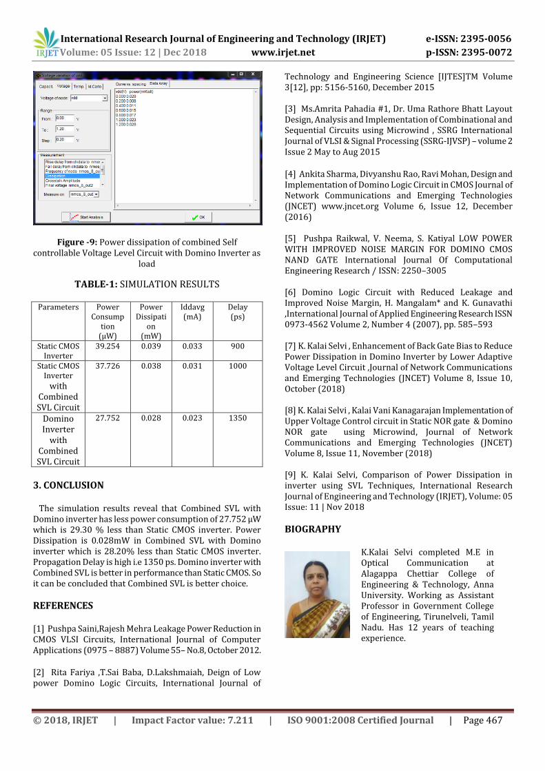
Figure -9: Power dissipation of combined Self controllable Voltage Level Circuit with Domino Inverter as
load
TABLE-1: SIMULATION RESULTS
Parameters Power Consump
tion (μW)
Power Dissipati
on (mW)
Iddavg (mA)
Delay (ps)
Static CMOS Inverter
39.254 0.039 0.033 900
Static CMOS Inverter
with Combined SVL Circuit
37.726 0.038 0.031 1000
Domino Inverter
with Combined SVL Circuit
27.752 0.028 0.023 1350
3. CONCLUSION The simulation results reveal that Combined SVL with Domino inverter has less power consumption of 27.752 μW which is 29.30 % less than Static CMOS inverter. Power Dissipation is 0.028mW in Combined SVL with Domino inverter which is 28.20% less than Static CMOS inverter. Propagation Delay is high i.e 1350 ps. Domino inverter with Combined SVL is better in performance than Static CMOS. So it can be concluded that Combined SVL is better choice.
REFERENCES [1] Pushpa Saini,Rajesh Mehra Leakage Power Reduction in CMOS VLSI Circuits, International Journal of Computer Applications (0975 – 8887) Volume 55– No.8, October 2012. [2] Rita Fariya ,T.Sai Baba, D.Lakshmaiah, Deign of Low power Domino Logic Circuits, International Journal of
Technology and Engineering Science [IJTES]TM Volume 3[12], pp: 5156-5160, December 2015 [3] Ms.Amrita Pahadia #1, Dr. Uma Rathore Bhatt Layout Design, Analysis and Implementation of Combinational and Sequential Circuits using Microwind , SSRG International Journal of VLSI & Signal Processing (SSRG-IJVSP) – volume 2 Issue 2 May to Aug 2015 [4] Ankita Sharma, Divyanshu Rao, Ravi Mohan, Design and Implementation of Domino Logic Circuit in CMOS Journal of Network Communications and Emerging Technologies (JNCET) www.jncet.org Volume 6, Issue 12, December (2016) [5] Pushpa Raikwal, V. Neema, S. Katiyal LOW POWER WITH IMPROVED NOISE MARGIN FOR DOMINO CMOS NAND GATE International Journal Of Computational Engineering Research / ISSN: 2250–3005 [6] Domino Logic Circuit with Reduced Leakage and Improved Noise Margin, H. Mangalam* and K. Gunavathi ,International Journal of Applied Engineering Research ISSN 0973-4562 Volume 2, Number 4 (2007), pp. 585–593 [7] K. Kalai Selvi , Enhancement of Back Gate Bias to Reduce Power Dissipation in Domino Inverter by Lower Adaptive Voltage Level Circuit ,Journal of Network Communications and Emerging Technologies (JNCET) Volume 8, Issue 10, October (2018) [8] K. Kalai Selvi , Kalai Vani Kanagarajan Implementation of Upper Voltage Control circuit in Static NOR gate & Domino NOR gate using Microwind, Journal of Network Communications and Emerging Technologies (JNCET) Volume 8, Issue 11, November (2018) [9] K. Kalai Selvi, Comparison of Power Dissipation in inverter using SVL Techniques, International Research Journal of Engineering and Technology (IRJET), Volume: 05 Issue: 11 | Nov 2018
BIOGRAPHY
K.Kalai Selvi completed M.E in Optical Communication at Alagappa Chettiar College of Engineering & Technology, Anna University. Working as Assistant Professor in Government College of Engineering, Tirunelveli, Tamil Nadu. Has 12 years of teaching experience.