implementation of all-optical logic and gate using … · implementation of all-optical logic and...
TRANSCRIPT

Photonic Research Center
Implementation of All-Optical Logic AND Gate using XGM based on Semiconductor Optical Amplifiers
Sang H. Kim 1, J. H. Kim1,2, C. W. Son1, G. Kim1, Y. T. Byun1, Y. M. Jhon1, S. Lee1, D. H. Woo1, and S. H. Kim1
1Photonics Research Center, Korea Institute of Science and Technology, 39-1 Hawolgok, Seongbuk, Seoul 136-791, Korea, Phone :+82-02-98-6705, Fax:+82-958-5709, e-mail: [email protected]
2Department of Electrical Engineering, Pennsylvania State University, University Park, PA 16802, USA

Photonic Research CenterContents
Introduction
What is a Cross Gain Modulation?
Previous All-Optical AND Gate
Basic Operation
Simulation for Logic AND
Experimental Setup
Experimental Results
Conclusions
Photonic Research Center
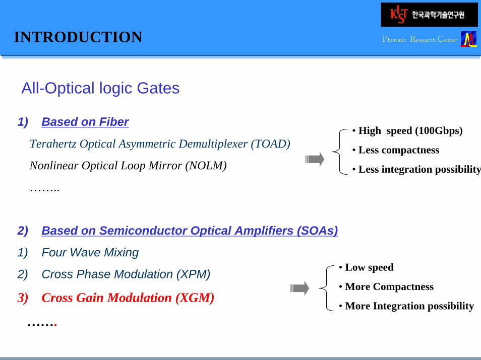
1) Based on Fiber
Terahertz Optical Asymmetric Demultiplexer (TOAD)
Nonlinear Optical Loop Mirror (NOLM)
……..
2) Based on Semiconductor Optical Amplifiers (SOAs)
1) Four Wave Mixing
2) Cross Phase Modulation (XPM)
3) Cross Gain Modulation (XGM)
…….
All-Optical logic Gates
• High speed (100Gbps)
• Less compactness
• Less integration possibility
• Low speed
• More Compactness
• More Integration possibility
INTRODUCTION
Photonic Research Center
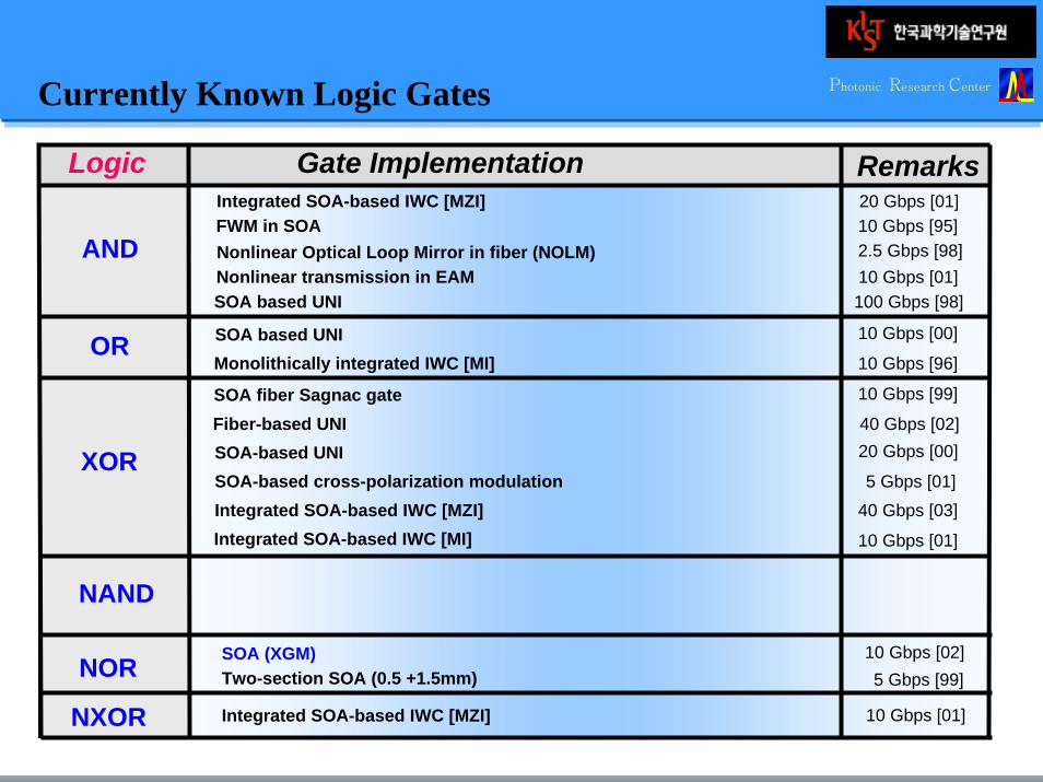
AND
OR
XOR
NAND
NOR
NXOR
Logic Gate Implementation
FWM in SOANonlinear Optical Loop Mirror in fiber (NOLM)Nonlinear transmission in EAMSOA based UNI
SOA based UNIMonolithically integrated IWC [MI]
SOA fiber Sagnac gateFiber-based UNISOA-based UNISOA-based cross-polarization modulationIntegrated SOA-based IWC [MZI]Integrated SOA-based IWC [MI]
SOA (XGM)Two-section SOA (0.5 +1.5mm)
Integrated SOA-based IWC [MZI]
Remarks
10 Gbps [95]2.5 Gbps [98]10 Gbps [01]100 Gbps [98]
10 Gbps [00]
10 Gbps [96]
10 Gbps [99]
40 Gbps [02]20 Gbps [00]
5 Gbps [01]40 Gbps [03]
10 Gbps [01]
10 Gbps [02]5 Gbps [99]
10 Gbps [01]
Integrated SOA-based IWC [MZI] 20 Gbps [01]
Currently Known Logic Gates

Photonic Research CenterWhy Logic Gates based on XGM?
• Higher compactness compared to UNI and TOAD
• Simple and Stable compared to other optical logic gates
• Potentially independent on polarization and wavelength
• Potentially transparent
• Integration capable
• Low switching energy

Photonic Research Center
XOR Type PerformanceContrast ratio at 10Gb/s
Repeated Operation speed
Energy No. of SOA(s)
Bit-pattern Dependence
Polarization Sensitive
Integration Potential
XOR Based-on Kerr Effect in Fiber
NOLM-based XOR 10dB 100Gb/s High 0 Very low No Weak
XOR Using CPM in SOA Poor 5/10/20Gb/s Moderate 1 High Very Strong
XOR Using FWM in SOA 20dB 2.5/10/20Gb/s Low 1 Low Yes Strong
XOR Using XGM in SOA 11dB 5/10Gb/s Moderate 1 or 2 Low Not so Strong
TOAD-based XOR 11dB 10Gb/s Moderate 1 Moderate Yes Weak
UNI-based XOR 20/40Gb/s Low 1 Low Yes Weak
XOR Using XPM in SOA-MZI
13~15.5dB 10/20/40Gb/s Low 2Low if with Differential Scheme
Yes Strong
XOR Using XGM in SOA-MZI
Moderate 2Low if with Differential Scheme
No Strong
XOR Based-on SOA-Assisted Integrated Interferometer
XOR Based on SOA-Assisted Fiber Interferometer
XOR Using Nonlinear Effects in SOA itself
Min Zhang, Ling Wang, Peida Ye, “All optical XOR logic gates: technologies and experiment demonstrations, IEEE Communications Magazines, 43, 19-24(2005).
A Comparison of the performance among the XOR gates using various schemes

Photonic Research Center
Probe signal (CW)
Input (dBm) - (pump signal)O
utpu
t (a.
u.)
Converted Signal
(Wavelength ofProbe signal)
Input Signal
SOACW
Static CharacteristicsGain saturation
- 4
- 3
- 2
- 1
0
1
2
- 15 - 10 - 5 0 5 10Input signal (dBm)
Out
puts
igna
l(a.
u.)
NRZ signal at Low Speed
XGM Wavelength Conversion?

Photonic Research Center
RZ signal at High Speed
Probe signal – continuous pulse train
Input (dBm) - (pump signal)O
utpu
t (a.
u.)
Converted Signal
(Wavelength ofProbe signal)
Input Signal
0 1 0 1
1 0 0 1
More than3dB
XGM Wavelength Conversion
Cross gain modulation?
The carrier density changes in SOA a signal at one wavelength affect the gain of signal at another wavelength using carrier density change in SOA.
SOAClock

Photonic Research Center
SOA
pumpprobepumpprobe signalsignalSOAofFunctionBoolean ⋅=,
probesignal
pumpprobe signalsignal ⋅
pumpsignal
clockSOA
1
pumppumpprobe,pump signalsignalSOAofFunctionBoolean =⋅= 1
pumpsignal
pumpsignal
All-optical Logic Functions Using XGM

Photonic Research Center
SOA-1clock B
B
SOA-2A X
XA ⋅
BA)B(AXAOutputSOA ⋅=⋅=⋅=−2
)B(BClockOutput SOA =⋅=−1
Previous All-Optical AND Gate
J. H. Kim et al., “All-Optical AND Gate Using Cross-Gain Modulation in Semiconductor Optical Amplifiers,”
Jpn. J. of Appl. Phys. 43, 608-610 (2004).
It requires 3 input signals!!!!!!

Photonic Research Center
J. H. Kim et al., “All-Optical AND Gate Using Cross-Gain Modulation in Semiconductor Optical Amplifiers,”
Jpn. J. of Appl. Phys. 43, 608-610 (2004).
Previous Experimental Setup
Input signal
Fiber Ring Laser pulse
Attenuator
Optical delay
PolarizationController (PC)
Signal Analyzer
PD
Photo-detector
SOA-1
EDFA-1
B
CLOCKCirculator
Attenuator
Optical delay
PC
Delay of 200 ps B
SOA-2
EDFA-2
Optical delay Delay of 100 ps
Delay of 100 psOperation speedof 2.5 Gb/s
A
AB
EDFA
Input signal
Fiber Ring Laser pulse
Attenuator
Optical delay
PolarizationController (PC)
Signal Analyzer
PD
Photo-detector
SOA-1
EDFA-1
B
CLOCKCirculator
Attenuator
Optical delay
PC
Delay of 200 ps B
SOA-2
EDFA-2
Optical delay Delay of 100 ps
Delay of 100 psOperation speedof 2.5 Gb/s
A
AB
EDFA
B
A
B
CLK
AND
Setup for All-Optical logic AND 10Gbps All-Optical logic AND

Photonic Research Center
SOA-1A B
BA ⋅
SOA-2ABA ⋅
BAOutput SOA ⋅=−1
BABAAA)BA(A)BA(AXAOutputSOA
⋅=⋅+⋅=
+⋅=⋅=⋅=−2
New AND without Clock Signal
It requires 2 Input signals !!!!!!

Photonic Research CenterSetup for simulation results

Photonic Research CenterSimulation results for implementing logic AND

Photonic Research Center
Experimental Setup for Logic AND
SOA-1
SOA-2Oscilloscope
PC Att
B
1X2
ANDOscilloscope
B
SOA-1
SOA-2OscilloscopeOscilloscope
EDFA-2
B
ANDOscilloscope
FRL
VOD
A
BEDFA-1
OC-1
OC-2
SA
OI

Photonic Research Center
Inputs and Output in SOA-1
A
B
BA •
1 1 0 0
0 1 1 0
1 0 0 0
Experimental Oscilloscope Traces of Input data pattern and Output data pattern in SOA-1 and SOA-2
BA •
A
BA •
1 1 0 0
1 0 0 0
0 1 0 0
Inputs and Output in SOA-2
Experiment Results
Photonic Research CenterConclusions
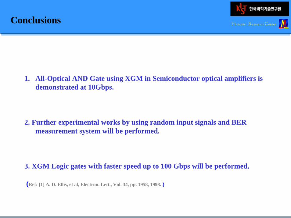
1. All-Optical AND Gate using XGM in Semiconductor optical amplifiers is demonstrated at 10Gbps.
2. Further experimental works by using random input signals and BER measurement system will be performed.
3. XGM Logic gates with faster speed up to 100 Gbps will be performed.
(Ref: [1] A. D. Ellis, et al, Electron. Lett., Vol. 34, pp. 1958, 1998. )