impedance and electrical models - pearson higher ed
TRANSCRIPT

79
C
H A P T E R
3
Impedance and Electrical Models
In high-speed digital systems, where signal integrity plays a significant role,we often refer to signals as either changing voltages or a changing currents. Allthe effects that we lump in the general category of signal integrity are due to howanalog signals (those changing voltages and currents) interact with the electricalproperties of the interconnects. The key electrical property with which signalsinteract is the impedance of the interconnects.
Impedance is defined as the ratio of the voltage to the current. We usuallyuse the letter Z to represent impedance. The definition, which is
always
true, isZ = V/I. The manner in which these fundamental quantities, voltage and cur-rent, interact with the impedance of the interconnects determines all signal-integrity effects. As a signal propagates down an interconnect, it is constantlyprobing the impedance of the interconnect and reacting based on the answer.
Likewise, if we have a target spec for performance and know what the sig-nals will be, we can sometimes specify an impedance specification for the inter-connects. If we understand how the geometry and material properties affect the
T I P
If we know the impedance of the interconnect, we canaccurately predict how the signals will be distorted and whether adesign will meet the performance specification, before we build it.

80 Chapter 3 • Impedance and Electrical Models
impedance of the interconnects, then we will be able to design the cross section,the topology, and the materials and select the other components so they will meetthe impedance spec and result in a product that works the first time.
3.1 Describing Signal-Integrity Solutions in Terms of Impedance
Each of the four basic families of signal-integrity problems can be describedbased on impedance.
1.
Signal-quality problems arise because voltage signals reflect and are dis-torted whenever the impedance the signal sees changes. If the impedance the signal sees is always constant, there will be no reflection and the signal will continue undistorted. Attenuation effects are due to series and shunt-resistive impedances.
2.
Cross talk arises from the electric and magnetic fields coupling between two adjacent signal traces (and, of course, their return paths). The mutual capaci-tance and mutual inductance between the traces establishes an impedance, which determines the amount of coupled current.
3.
Rail collapse of the voltage supply is really about the impedance in the power-distribution system (PDS). A certain amount of current must flow to feed all the ICs in the system. Because of the impedance of the power and ground distribution, a voltage drop will occur as the IC current switches. This voltage drop means the power and ground rails have collapsed from their nominal values.
4.
The greatest source of EMI is from common-mode currents, driven by volt-ages in the ground planes, through external cables. The higher the imped-ance of the return current paths in the ground planes, the greater the voltage drop, or ground bounce, which will drive the radiating currents. The most common fix for EMI from cables is the use of a ferrite choke around the cable. This works by increasing the impedance the common-mode currents see, thereby reducing the amount of common-mode current.
There are a number of design rules, or guidelines, that establish constraintson the physical features of the interconnects. For example, “keep the spacing
T I P
Impedance is the key term that describes every impor-tant electrical property of an interconnect. Knowing the imped-ance and propagation delay of an interconnect is to know almosteverything about it electrically.

Describing Signal-Integrity Solutions in Terms of Impedance 81
between adjacent signal traces greater than 10 mils” is a design rule to minimizecross talk. “Use power and ground planes on adjacent layers separated by lessthan 5 mils” is a design rule for the power and ground distribution.
These rules establish a specific impedance for the physical interconnects.This impedance provides a specific environment for the signals, resulting in adesired performance. For example, keeping the power and ground planes closelyspaced will result in a low impedance for the power distribution system and hencea lower voltage drop for a given power and ground current. This helps minimizerail collapse and EMI.
If we understand how the physical design of the interconnects affects theirimpedance, we will be able to interpret how they will interact with signals andwhat performance they might have.
Impedance is at the heart of the methodology we will use to solve signal-integrity problems. Once we have designed the physical system as we think itshould be for optimal performance, we will translate the physical structure into itsequivalent electrical circuit model. This process is called modeling.
It is the impedance of the resulting circuit model that will determine how theinterconnects will affect the voltage and current signals. Once we have the circuitmodel, we will use a circuit simulator, such as SPICE, to predict the new wave-forms as the voltage sources are affected by the impedances of the interconnects.Alternatively, behavioral models of the drivers or interconnects can be used wherethe interaction of the signals with the impedance, described by the behavioralmodel, will predict performance. This process is called simulation.
Finally, the predicted waveforms will be analyzed to determine if they meetthe timing and distortion or noise specs, and are acceptable, or if the physicaldesign has to be modified. This process flow for a new design is illustrated inFigure 3-1.
T I P
Not only are the problems associated with signal integritybest described by the use of impedance, but the solutions andthe design methodology for good signal integrity are also basedon the use of impedance.
T I P
Impedance is the Rosetta stone that links physicaldesign and electrical performance. Our strategy is to translatesystem-performance needs into an impedance requirement andphysical design into an impedance property.

82 Chapter 3 • Impedance and Electrical Models
The two key processes, modeling and simulation, are based on convertingelectrical properties into an impedance, and analyzing the impact of the imped-ance on the signals.
If we understand the impedance of each of the circuit elements used in aschematic and how the impedance is calculated for a combination of circuit ele-ments, the electrical behavior of
any
model and
any
interconnect can be evaluated.This concept of impedance is absolutely critical in all aspects of signal-integrityanalysis.
3.2 What Is Impedance?
We use the term
impedance
in everyday language and often confuse the elec-trical definition with the common usage definition. As we saw earlier, the electricalterm
impedance
has a very precise definition based on the relationship between thecurrent through a device and the voltage across it: Z = V/I. This basic definitionapplies to any two-terminal device, such as a surface mount resistor, a decouplingcapacitor, a lead in a package, or the front connections to a printed circuit-boardtrace and its return path. When there are more than two terminals, such as in cou-pled conductors, or between the front and back ends of a transmission line, the def-inition of impedance is the same, it’s just more complex to take into account theadditional terminals.
For two-terminal devices, the definition of impedance, as illustrated inFigure 3-2, is simply:
Figure 3-1 Process flow for hardware design. The modeling, simulation,and evaluation steps should be implemented as early and often in the de-sign cycle as possible.
Specifications
Chip design/selection
Board design/component selection
Modeling
Simulation
Performance evaluation

What Is Impedance? 83
(3-1)
where:
Z = the impedance, measured in Ohms
V = the voltage across the device, in units of volts
I = the current through the device, in units of Amps
For example, if the voltage across a terminating resistor is 5 v and the cur-rent through it is 0.1 A, then the impedance of the device must be 5 v/0.1 A = 50Ohms. No matter what type of device the impedance is referring to, in both thetime and the frequency domain, the units of impedance are always in Ohms.
If we always go back to this basic definition, we will never go wrong andoftentimes eliminate many sources of confusion. One aspect of impedance that isoften confusing is to think of it only in terms of resistance. As we shall see, theimpedance of an ideal resistor-circuit element, with resistance, R, is, in fact, Z = R.
Our intuition of the impedance of a resistor is that a high impedance meansless current flow for a fixed voltage. Likewise, a low impedance means a lot ofcurrent can flow for the same voltage. This is consistent with the definition that I =V/Z, and applies just as well when the voltage or current is not DC.
T I P
This definition of impedance applies to absolutely all situ-ations, whether in the time domain or the frequency domain,whether for real devices that are measured or for ideal devicesthat are calculated.
Z VI----=
Figure 3-2 The definition of impedance for any two-terminal deviceshowing the current through the component and the voltage across theleads.
+
-
V I

84 Chapter 3 • Impedance and Electrical Models
In addition to the notion of the impedance of a resistor, the concept ofimpedance can apply to an ideal capacitor, an ideal inductor, a real-wire bond, aprinted circuit trace, or even a pair of connector pins.
There are two special extreme cases of impedance. For a device that is anopen, there will be no current flow. If the current through the device for any volt-age applied is zero, the impedance is Z = 1 v / 0 A = infinite Ohms. The imped-ance of an open device is very, very large. When the device is a short, there will beno voltage across it, no matter what the current through it. The impedance of ashort is Z = 0 v / 1 A = 0 Ohms. The impedance of a short is always 0 Ohms.
3.3 Real vs. Ideal Circuit Elements
There are two types of electrical devices, real and ideal. Real devices can bemeasured. They are the only things that physically exist. They are the actual inter-connects or components that make up the hardware of a real system. Real devicesare traces on a board, leads in a package, or discrete decoupling capacitorsmounted to a board.
Ideal devices are mathematical descriptions of specialized circuit elementsthat have precise, specific definitions. Simulators can only simulate the perfor-mance of ideal devices. The formalism and power of circuit theory apply only toideal devices. Models are composed of combinations of ideal devices.
It is very important to keep separate real versus ideal circuit elements. Theimpedance of any real, physical interconnect or passive component can be mea-sured. However, when impedance is calculated, it is only the impedance of fourvery-well-defined, ideal circuit elements that can be considered. We cannot mea-sure ideal circuit elements, nor can we calculate the impedance of any circuit ele-ments other than ideal ones. This is why it is important to make the distinctionbetween real components and ideal circuit elements. This distinction is illustratedin Figure 3-3.
A circuit model will always be an approximation of the real-world structure.However, it is possible to construct an ideal model with a simulated impedancewhich accurately matches the measured impedance of a real device. For example,Figure 3-4 shows the measured impedance of a real decoupling capacitor and the
T I P
Ultimately, our goal is to create an equivalent circuitmodel composed of combinations of ideal circuit elements whoseimpedance closely approximates the actual, measured imped-ance of a real component.

Real vs. Ideal Circuit Elements 85
simulated impedance based on an RLC circuit model. These are the componentand model in Figure 3-3. The agreement is excellent even up to 5 GHz, the band-width of the measurement.
There are four ideal, two-terminal, circuit elements that we will use in com-bination as building blocks to describe any real interconnect:
Figure 3-3 The two worldviews of a component, in this case a 1206 de-coupling capacitor mounted to a circuit board and an equivalent circuitmodel composed of combinations of ideal circuit elements.
Real physicalcomponent
Equivalent electrical circuitmodel of ideal circuit elements:
C = 0.67 nF
R = 0.50 ΩL = 1.78 nH
R L C
Topology:
Parasitic values:
Impe
danc
e, O
hms
Figure 3-4 The measured impedance, as circles, and the simulated im-pedance, as the line, for a nominal 1-nF decoupling capacitor. The mea-surement was performed with a network analyzer and a GigaTest LabsProbe Station.

86 Chapter 3 • Impedance and Electrical Models
1.
A resistor
2.
A capacitor
3.
An inductor
4.
A transmission line
We usually group the first three elements in a category called “lumped cir-cuit elements,” in the sense that their properties can be lumped into a single point.This is different from the properties of an ideal transmission line, which are “dis-tributed” along its length.
As ideal circuit elements, these elements have precise definitions thatdescribe how they interact with currents and voltages. It is very important to keepin mind that ideal elements are different from real components, such as real resis-tors, real capacitors, or real inductors. One is a physical component, the other anideal element.
The properties of a transmission line are initially seen as so confusing andnon-intuitive, yet so important, that we devote an entire chapter to transmissionlines and their impedance. In this chapter, we will concentrate on the impedanceof just R, L, and C elements.
An equivalent electrical circuit model is an idealized electrical description ofa real structure. It is an approximation, based on using combinations of ideal cir-cuit elements. A good model will have a calculated impedance that closelymatches the measured impedance of the real device. The better we can model theimpedance of an interconnect, the better we can predict how a signal will interactwith it.
When dealing with some high-frequency effects, such as lossy lines, we willneed to invent new ideal circuit elements to create better models.
3.4 Impedance of an Ideal Resistor in the Time Domain
Each of the four basic circuit elements above has a definition of how voltageand current interact with it. This is different from the impedance of the ideal cir-cuit element.
The relationship between the voltage across and the current through an idealresistor is:
T I P
Only real devices can be measured, and only ideal ele-ments can be calculated or simulated.

Impedance of an Ideal Capacitor in the Time Domain 87
(3-2)
where:
V = the voltage across the ends of the resistor
I = the current through the resistor
R = the resistance of the resistor, in Ohms
An ideal resistor has a voltage across it that increases with the current through it.This definition of the I-V properties of an ideal resistor applies in both the timedomain and the frequency domain.
In the time domain, we can apply the definition of the impedance and, usingthe definition of the ideal element, calculate the impedance of an ideal resistor:
(3-3)
This basically says, the impedance is constant and independent of the current orvoltage across a resistor. The impedance of a resistor is pretty boring.
3.5 Impedance of an Ideal Capacitor in the Time Domain
In an ideal capacitor, there is a relationship between the charge storedbetween the two leads and the voltage across the leads. The capacitance of anideal capacitor is defined as:
(3-4)
where:
C = the capacitance, in Farads
V = the voltage across the leads, in volts
Q = the charge stored between the leads, in Coulombs
V I R×=
Z VI---- I R×
I------------ R= = =
C QV----=
88 Chapter 3 • Impedance and Electrical Models
The value of the capacitance of a capacitor describes its capacity to store charge atthe expense of voltage. A large capacitance means the ability to store a lot ofcharge at a low voltage across the terminals.
The impedance of a capacitor can only be calculated based on the currentthrough it and the voltage across its terminals. In order to relate the voltage acrossthe terminals with the current through it, we need to know how the current flowsthrough a capacitor. A real capacitor is made from two conductors separated by adielectric. How does current get from one conductor to the other, when it has aninsulating dielectric between them? This is a fundamental question and will popup over and over in signal integrity applications.
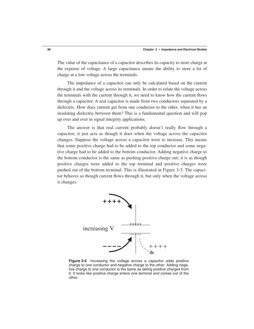
The answer is that real current probably doesn’t really flow through acapacitor, it just acts as though it does when the voltage across the capacitorchanges. Suppose the voltage across a capacitor were to increase. This meansthat some positive charge had to be added to the top conductor and some nega-tive charge had to be added to the bottom conductor. Adding negative charge tothe bottom conductor is the same as pushing positive charge out; it is as thoughpositive charges were added to the top terminal and positive charges werepushed out of the bottom terminal. This is illustrated in Figure 3-5. The capaci-tor behaves as though current flows through it, but only when the voltage acrossit changes.
Figure 3-5 Increasing the voltage across a capacitor adds positivecharge to one conductor and negative charge to the other. Adding nega-tive charge to one conductor is the same as taking positive charges fromit. It looks like positive charge enters one terminal and comes out of theother.
+++++
-----
++++
---- ++++
increasing V

Impedance of an Ideal Capacitor in the Time Domain 89
By taking derivatives of both sides of the previous equation, a new definitionof the I-V behavior of a capacitor can be developed:
(3-5)
where:
I = the current through the capacitor
Q = the charge on one conductor of the capacitor
C = the capacitance of the capacitor
V = the voltage across the capacitor
This relationship points out, as we saw previously, that the only way currentflows through a capacitor is when the voltage across it changes. If the voltage isconstant, the current through a capacitor is zero. We also saw that for a resistor,the current through it doubled if the current doubled. However, in the case of acapacitor, the current through it doubles if the rate of change of the voltage acrossit doubles.
This definition is consistent with our intuition. If the voltage changes rap-idly, the current through a capacitor is large. If the voltage is nearly constant, thecurrent through a capacitor is near zero. Using this relationship, we can calculatethe impedance of an ideal capacitor in the time domain:
(3-6)
where:
V = the voltage across the capacitor
C = the capacitance of the capacitor
I = the current through the capacitor
This is a complicated expression. It says that the impedance of a capacitordepends on the precise shape of the voltage waveform across it. If the slope of thewaveform is large (i.e., if the voltage changes very fast), the current through it ishigh and the impedance is small. It also says that a large capacitor will have
I dQdt------- C
dVdt-------= =
Z VI---- V
CdVdt-------
------------= =

90 Chapter 3 • Impedance and Electrical Models
a lower impedance than a small capacitor for the same rate of change of the volt-age signal.
However, the precise value of the impedance of a capacitor is more compli-cated. It is hard to generalize what the impedance of a capacitor is other than itdepends on the shape of the voltage waveform. The impedance of a capacitor isnot an easy term to use in the time domain.
3.6 Impedance of an Ideal Inductor in the Time Domain
The behavior of an ideal inductor is defined by:
(3-7)
where:
V = the voltage across the inductor
L = the inductance of the inductor
I = the current through the inductor
This says that the voltage across an inductor depends on how fast the currentthrough it changes. If the current is constant, the voltage across the inductor willbe zero. Likewise, if the current changes rapidly through an inductor, there will bea large voltage drop across it. The inductance is the proportionality constant thatsays how sensitive the voltage generated is to a changing current. A large induc-tance means that a small changing current produces a large voltage.
There is often confusion about the direction of the voltage drop that is gener-ated across an inductor. If the direction of the changing current reverses, the polar-ity of the induced voltage will reverse. An easy way of remembering the polarityof the voltage is to base it on the voltage drop of a resistor.
If a DC current goes through a resistor, the terminal the current goes into isthe positive side and the other terminal is the negative side. Likewise, with aninductor, the terminal the current is increasing into is the positive side and theother is the negative side for the induced voltage. This is illustrated in Figure 3-6.
Using this basic definition of inductance, we can calculate the impedance ofan inductor. This is, by definition, the ratio of the voltage to the current through aninductor:
V LdIdt-----=

Impedance of an Ideal Inductor in the Time Domain 91
(3-8)
where:
V = the voltage across the inductor
L = the inductance of the inductor
I = the current through the inductor
Again, we see the impedance of an inductor, though well defined, is awk-ward to use in the time domain. The general features are easy to discern. If thecurrent through an inductor increases rapidly, the impedance of the inductor islarge. An inductor will have a high impedance when current through it tries tochange. If the current through an inductor changes only slightly, its impedancewill be very small. For DC current the impedance of an inductor is nearly zero.But, other than these simple generalities, the actual impedance of an inductordepends very strongly on the precise waveform of the current through it.
T I P
For both the capacitor and the inductor, the impedance,in the time domain, is not a simple function at all. Impedance inthe time domain is a very complicated way of describing thesebasic building-block ideal circuit elements. It is not wrong, it is justcomplicated.
Figure 3-6 The direction of voltage drop across an inductor for a chang-ing current is in the same direction as the voltage drop across a resistorfor a DC current.
+ -
I
+ -
dI/dt
Z VI---- L
dIdt-----
I-----= =

92 Chapter 3 • Impedance and Electrical Models
This is one of the important occasions where moving to the frequencydomain will make the analysis of a problem much simpler.
3.7 Impedance in the Frequency Domain
The important feature of the frequency domain is that the only waveformsthat can exist are sine waves. We can only describe the behavior of ideal circuitelements in the frequency domain by how they interact with sine waves: sinewaves of current and sine waves of voltage. These sine waves have three and onlythree features: the frequency, the amplitude, and the phase associated with eachwave.
Rather than describe the phase in cycles or degrees, it is more common touse radians. There are 2 x
π
radians in one cycle, so a radian is about 57 degrees.The frequency in radians per second is referred to as the angular frequency. TheGreek letter omega (
ω
) is used to denote the angular frequency.
ω
is related to thefrequency, by:
(3-9)
where:
ω
= the angular frequency, in radians/sec
f = the sine-wave frequency, in Hertz
We can apply sine-wave voltages across a circuit element and look at thesine waves of current through it. When we do this, we will still use the same basicdefinition of impedance (that is, the ratio of the voltage to the current) except thatwe will be taking the ratio of two sine waves, a voltage sine wave and a currentsine wave.
It is important to keep in mind that all the basic building-block circuit ele-ments and all the interconnects are linear devices. If a voltage sine wave of1 MHz, for example, is applied across any of the four ideal circuit elements, theonly sine-wave-frequency components that will be present in the current wave-form will be a sine wave at 1 MHz. The amplitude of the current sine wave willbe some number of Amps and it will have some phase shift with respect to thevoltage wave, but it will have exactly the same frequency. This is illustrated inFigure 3-7.
ω 2π f×=

Impedance in the Frequency Domain 93
What does it mean to take the ratio of two sine waves, the voltage and thecurrent? The ratio of two sine waves is not a sine wave. It is a pair of numbers thatcontains information about the ratio of the amplitudes and the phase shift, at eachfrequency value. The magnitude of the ratio is just the ratio of the amplitudes ofthe two sine waves:
(3-10)
The ratio of the voltage amplitude to the current amplitude will have units ofOhms. We refer to this ratio as the magnitude of the impedance. The phase of theratio is the phase shift between the two waves. The phase shift has units of degreesor radians. In the frequency domain, the impedance of a circuit element or combi-nation of circuit elements would be of the form: at 20 MHz, the magnitude of theimpedance is 15 Ohms and the phase of the impedance is 25 degrees. This meansthe impedance is 15 Ohms and the voltage wave is leading the current wave by25 degrees.
T I P
When we take the ratio of two sine waves, we need toaccount for the ratio of the amplitudes and the phase shiftbetween the two waves.
Figure 3-7 The sine-wave current through and voltage across an idealcircuit element will have exactly the same frequency but different ampli-tudes and some phase shift.
current
voltage
time
Z VI
-------=

94 Chapter 3 • Impedance and Electrical Models
The impedance of any circuit element is two numbers, a magnitude and aphase, at every frequency value. Both the magnitude of the impedance and thephase of the impedance may be frequency dependent. The ratio of the amplitudesmay vary with frequency or the phase may vary with frequency. When wedescribe the impedance, we need to specify at what frequency we are describingthe impedance.
In the frequency domain, impedance can also be described with complexnumbers. For example, the impedance of a circuit can be described as having areal component and an imaginary component. The use of real and imaginary com-ponents allows the powerful formalism of complex numbers to be applied, whichdramatically simplifies the calculations of impedance in large circuits. Exactly thesame information is contained in the magnitude and the phase information. Theseare two different and equivalent ways of describing impedance.
With this new idea of working in the frequency domain, and dealing onlywith sine waves of current and voltage, we can take another look at impedance.
We apply a sine wave of current through a resistor and we get a sine wave ofvoltage across it that is simply R times the current wave:
(3-11)
We can describe the sine wave of current in terms of sine and cosine waves or interms of complex exponential notation.
When we take the ratio of the voltage to the current for a resistor, we findthat it is simply the value of the resistance:
(3-12)
The impedance is independent of frequency and the phase shift is zero. Theimpedance of an ideal resistor is flat with frequency. This is basically the sameresult we saw in the time domain, still pretty boring.
When we look at an ideal capacitor in the frequency domain, we will apply asine-wave voltage across the ends. The current through the capacitor is the deriva-tive of the voltage, which is a cosine wave:
V I0 ωt( )sin R×=
Z VI----
I0 ωt( )sin R×I0 ωt( )sin
--------------------------------- R= = =

Impedance in the Frequency Domain 95
(3-13)
This says the current amplitude will increase with frequency, even if thevoltage amplitude stays constant. The higher the frequency, the larger the ampli-tude of the current through the capacitor. This suggests the impedance of a capac-itor will decrease with increasing frequency. The impedance of a capacitor iscalculated from:
(3-14)
Here is where it gets confusing. This ratio is easily described using complexmath, but most of the insight can also be gained from sine and cosine waves. Themagnitude of the impedance of a capacitor is just 1/
ω
C. All the important infor-mation is here. As the angular frequency increases, the impedance of a capacitordecreases. This says that even though the value of the capacitance is constant withfrequency, the impedance gets smaller with higher frequency. We see this is rea-sonable because the current through the capacitor will increase with higher fre-quency and hence its impedance will be less.
The phase of the impedance is the phase shift between a sine and cosinewave, which is –90 degrees. When described in complex notation, the –90 degreephase shift is represented by the complex number, –i. In complex notation, theimpedance of a capacitor is –i/
ω
C. For most of the following discussion, the phaseadds more confusion than value and will generally be ignored.
A real decoupling capacitor has a capacitance of 10 nF. What is its imped-ance at 1 GHz? First, we assume this capacitor is an ideal capacitor. A 10-nFideal capacitor will have an impedance of 1/(2
π
×
1 GHz
×
10 nF) = 1/(6
×
10
9
×
10 x 10
-9) = 1/60 ~ 0.016 Ohms. This is a very small impedance. If the realdecoupling capacitor behaved like an ideal capacitor, its impedance would beabout 10 milliOhms at 1 GHz. Of course, at lower frequency, its impedancewould be higher. At 1 Hz, its impedance would be about 16 MegaOhms.
Let’s use this same frequency-domain analysis with an inductor. When weapply a sine wave current through an inductor, the voltage generated is:
I Ctd
d× V0 ωt( )sin C ω× V0 ωt( )cos= =
Z VI----
V0 ωt( )sin
C ω× V0 ωt( )cos-----------------------------------------
1ωC-------- ωt( )sin
ωt( )cos-------------------×= = =

96 Chapter 3 • Impedance and Electrical Models
(3-15)
This says that for a fixed current amplitude, the voltage across an inductor getslarger at higher frequency. It takes a higher voltage to push the same currentamplitude through an inductor. This would hint that the impedance of an inductorincreases with frequency.
Using the basic definition of impedance, the impedance of an inductor in thefrequency domain can be derived as:
(3-16)
The magnitude of the impedance increases with frequency, even though thevalue of the inductance is constant with frequency. It is a natural consequence ofthe behavior of an inductor that it is harder to shove AC current through it withincreasing frequency.
The phase of the impedance of an inductor is the phase shift between thevoltage and the current which is +90 degrees. In complex notation, a +90 degreephase shift is i. The complex impedance of an inductor is Z = iωL.
In a real decoupling capacitor, there is inductance associated with the intrin-sic shape of the capacitor and its board-attach footprint. A rough estimate for thisintrinsic inductance is 2 nH. We really have to work hard to get it any lower thanthis. What is the impedance of just the series inductance of the real capacitor thatwe will model as an ideal inductor of 2 nH, at a frequency of 1 GHz?
The impedance is Z = 2 × π × 1 GHz × 2 nH = 12 Ohms. When it is in serieswith the power and ground distribution and we want a low impedance, for exam-ple less than 0.1 Ohms, 12 Ohms is a lot. How does this compare with the imped-ance of the ideal-capacitor component of the real decoupling capacitor? In thelast problem, the impedance of the ideal capacitor element at 1 GHz was 0.01Ohm. The impedance of the ideal inductor component is more than 1000 timeshigher than this and will clearly dominate the high-frequency behavior of a realcapacitor.
We see that for both the ideal capacitor and inductor, the impedance in thefrequency domain has a very simple form and is easily described. This is one ofthe powers of the frequency domain and why we will often turn to it to help solveproblems.
V Ltd
d× I0 ωt( )sin L ω× I0 ωt( )cos= =
Z VI----
L ω× I0 ωt( )cos
I0 ωt( )sin--------------------------------------- ωL
ωt( )cosωt( )sin
-------------------×= = =
Equivalent Electrical Circuit Models 97
The value of the resistance, capacitance, and inductance of ideal resistors,capacitors, and inductors are all constant with frequency. For the case of an idealresistor, the impedance is also constant with frequency. However, for a capacitor,its impedance will decrease with frequency, and for an inductor, its impedancewill increase with frequency.
3.8 Equivalent Electrical Circuit Models
The impedance behavior of real interconnects can be closely approximatedby combinations of these ideal elements. A combination of ideal circuit elementsis called an equivalent electrical circuit model, or typically, just a model. Thedrawing of the circuit model is often referred to as a schematic.
An equivalent circuit model has two features: it identifies how the circuitelements are connected together (called the circuit topology) and it identifies thevalue of each circuit element (referred to as the parameter values or parasitic val-ues).
Chip designers, who like to think they produce drivers with perfect, pristinewaveforms, view all interconnects as parasitics in that they can only screw up theirwonderful waveforms. To the chip designer, the process of determining the param-eter values of the interconnects is really parasitic extraction, and the term hasstuck in general use.
There will always be a limit to how well we can predict the actual impedancebehavior of real interconnects, using an ideal equivalent circuit model. This limitcan often be found only by measuring the actual impedance of an interconnect andcomparing it to the predictions based on the simulations of circuits containingthese ideal circuit elements.
There are always two important questions to ask of every model: how goodis it and what is its bandwidth? Remember, its bandwidth is the highest sine-wave
T I P It is important to keep straight that for an ideal capacitoror inductor, even though its value of capacitance and inductanceis absolutely constant with frequency, its impedance will vary withfrequency.
T I P It is important to keep in mind that whenever we draw cir-cuit elements, they are always ideal circuit elements. We willhave to use combinations of ideal elements to approximate theactual performance of real interconnects.

98 Chapter 3 • Impedance and Electrical Models
frequency at which we get good agreement between the measured impedance andthe predicted impedance. As a general rule, the closer we would like the predic-tions of a circuit model to be to the actual measured performance, the more com-plex the model may have to be.
Take, for example, a real decoupling capacitor and its impedance as mea-sured from one of the capacitor pads, through a via and a plane below it, comingback up to the start of the capacitor. This is the example shown previously in Fig-ure 3-3. We might expect that this real device could be modeled as a simple idealcapacitor. But, at how high a frequency will the real capacitor still behave like anideal capacitor? The measured impedance of this real device, from 10 MHz to 5GHz, is shown in Figure 3-8, with the impedance predicted for an ideal capacitorsuperimposed.
It is clear that this simple model works really well at low frequency. Thissimple model of an ideal capacitor with a value of 0.67 nF is a very good model.It’s just that it gives good agreement only up to about 70 MHz. Its bandwidth is70 MHz.
T I P It is good practice to always start the process of modelingwith the simplest model possible and grow in complexity fromthere.
Figure 3-8 Comparison of the measured impedance of a real decou-pling capacitor and the predicted impedance of a simple first-order modelusing a single C element and a second-order model using an RLC circuitmodel. Measured with a GigaTest Labs Probe Station.
measured impedance
Impe
danc
e, O
hms
Frequency, Hz
first-ordercapacitor model
second-orderRLC model
Circuit Theory and SPICE 99
If we expend a little more effort, we can create a more accurate circuit modelwith a higher bandwidth. A more accurate model for a real decoupling capacitor isan ideal capacitor, inductor, and resistor in series. Choosing the best parametervalues, we see in Figure 3-8 that the agreement between the predicted impedanceof this model and the measured impedance of the real device is excellent, all theway up to the bandwidth of the measurement, 5 GHz in this case.
We often refer to the simplest model we create as a first-order model, as it isthe first starting place. As we increase the complexity, and hopefully, better agree-ment with the real device, we refer to each successive model as the second-ordermodel, third-order model, and so on.
Using the second-order model for a real capacitor would let us accuratelypredict every important electrical feature of this real capacitor as it would behavein a system with application bandwidths at least up to 5 GHz.
3.9 Circuit Theory and SPICE
There is a well-defined and relatively straightforward formalism to describethe impedance of combinations of ideal circuit elements. This is usually referredto as circuit theory. The important rule in circuit theory is that when two or moreelements are in series, that is, connected end-to-end, the impedance of the combi-nation, from one end terminal to the other end terminal, is the sum of the imped-ances of each element. What makes it a little complicated is that when in thefrequency domain, the impedances that are summed are complex and must obeycomplex algebra.
In the previous section, we saw that it is possible to calculate the impedanceof each individual circuit element by hand. When there are combinations of circuitelements it gets more complicated. For example, the impedance of an RLC modelapproximating a real capacitor is given by:
(3-17)
We could use this analytic expression for the impedance of the RLC circuitto plot the impedance versus frequency for any chosen values of R, L, and C. It
T I P It is remarkable that the relatively complex behavior ofreal components can be very accurately approximated, to veryhigh bandwidths, by combinations of ideal circuit elements.
Z ω( ) R i ωL 1ωC--------–
+=

100 Chapter 3 • Impedance and Electrical Models
can conveniently be used in a spreadsheet and each element changed. When thereare five or ten elements in the circuit model, the resulting impedance can be calcu-lated by hand, but it can be very complicated and tedious.
However, there is a commonly available tool that is much more versatile incalculating and plotting the impedance of any arbitrary circuit. It is so commonand so easy to use, every engineer who cares about impedance or circuits in gen-eral, should have access to it on their desktop. It is SPICE.
SPICE stands for Simulation Program with Integrated Circuit Emphasis. Itwas developed in the early 1970s at UC Berkeley as a tool to predict the behaviorof transistors based on the as-fabricated dimensions. It is basically a circuit simu-lator. Any circuit we can draw with R, L, C, and T elements can be simulated for avariety of voltage or current-exciting waveforms. It has evolved and diversifiedover the past 30 years, with over 30 vendors each adding their own special fea-tures and capabilities. There are a few either free versions or student versions forless than $100 that can be downloaded from the Web. Some of the free versionshave limited capability but are excellent tools to learn about circuits.
In SPICE, only ideal circuit elements are used and every circuit element hasa well-defined, precise behavior. There are two basic types of elements: active andpassive. The active elements are the signal sources, current or voltage waveforms,or actual transistor or gate models. The passive elements are all the ideal circuitelements described above. One of the distinctions between the various forms ofSPICE is the variety of ideal circuit elements they provide. Every version ofSPICE includes at least the R, L, C, and T (transmission-line) elements.
SPICE simulators allow the prediction of the voltage or current at everypoint in a circuit, simulated either in the time-domain or the frequency domain. Atime-domain simulation is called a transient simulation and a frequency-domainsimulation is called an AC simulation. SPICE is an incredibly powerful tool.
For example, a driver connected to two receivers located very close togethercan be modeled with a simple voltage source and an RLC circuit. The R is theimpedance of the driver, typically about 10 Ohms. The C is the capacitance of theinterconnect traces and the input capacitance of the two receivers, typically about5 pF total. The L is the total loop inductance of the package leads and the inter-connect traces, typically about 7 nH. The set-up of this circuit in SPICE and theresulting time-domain waveform, showing the ringing that might be found in theactual circuit, is shown in Figure 3-9.

Circuit Theory and SPICE 101
SPICE can be used to calculate and plot the impedance of any circuit in thefrequency domain. Normally, it plots only the voltage or current waveforms atevery connection point, but a trick can be used to convert this into impedance.
One of the circuit elements SPICE has in its toolbox for AC simulation is aconstant-current sine-wave-current source. This current source will output a sinewave of current, with a constant amplitude, at a predetermined frequency. Whenrunning an AC analysis, the SPICE engine will step the frequency of the sine-wave-current source from the start frequency value to the stop frequency valuewith a number of intermediate frequency points.
It generates the constant-current amplitude by outputting a sin wave voltage-amplitude sine wave. The amplitude of the voltage wave is automatically adjustedto result in the specified constant amplitude of current.
To build an impedance analyzer in SPICE, we set the current source to havea constant amplitude of 1 Amp. No matter what circuit elements are connected tothe current source, SPICE will adjust the voltage amplitude to result in 1-Amp
T I P If the circuit schematic can be drawn, SPICE can simu-late the voltage and current waveforms. This is the real power ofSPICE for general electrical engineering analysis.
Figure 3-9 Simple equivalent circuit model to represent a driver and re-ceiver fanout of two, including the packaging and interconnects, as set upin Agilent’s Advanced Design System (ADS), a version of SPICE, and theresulting simulation of the internal-voltage waveform and the voltage atthe input of the receivers. The rise time simulated is 0.5 nsec. The leadand interconnect inductance plus the input-gate capacitance dominatethe source of the ringing.
V_o
ut
TranTran2
MaxTimeStep = 0.1 nsecStopTime = 10 sec
TRANSIENT
t
1 2 3 4 5 6 7 8 90 10
1
2
3
4
5
6
7
0
8
Time

102 Chapter 3 • Impedance and Electrical Models
current amplitude through the circuit. If the constant-current source is connectedto a circuit that has some impedance associated with it, Z(ω), then to keep theamplitude of the current constant, the voltage it applies will have to adjust. Thevoltage applied to the circuit, from the constant-current source, with a 1-Amp cur-rent amplitude, is V(ω) = Z(ω) × 1 Amp. The voltage across the current source, involts, is numerically equal to the impedance of the circuit attached, in Ohms.
For example, if we attach a 1-Ohm resistor across the terminals, in order tomaintain the constant current of 1 Amp, the voltage amplitude generated must beV = 1 Ohm × 1A = 1 v. If we attach a capacitor with capacitance C, the voltageamplitude at any frequency will be V = 1/ωC. Effectively, this circuit will emulatean impedance analyzer. Plotting the voltage versus the frequency is a measure ofthe magnitude of the impedance versus frequency for any circuit. The phase of thevoltage is also a measure of the phase of the impedance.
To use SPICE to plot an impedance profile, we construct an AC constant-current source with amplitude of 1 A and connect the circuit under test acrossthe terminals. The voltage measured across the current source is a direct mea-sure of the impedance of the circuit. An example of a simple circuit is shown inFigure 3-10. As a trivial example, we connect a few different circuit elements tothe impedance analyzer and plot their impedance profiles.
We can use this impedance analyzer to plot the impedance of any circuitmodel. Impedance is complex. It has not only magnitude information but alsophase information. We can plot each of these separately in SPICE. The phase is
Figure 3-10 Left: An impedance analyzer in SPICE. The voltage acrossthe constant-current source is a direct measure of the impedance of thecircuit connected to it. Right: An example of the magnitude of the imped-ance of various circuit elements, calculated with the impedance analyzerin SPICE.
ACAC1
Stop = 10.0 GHzStart = 1.0 MHz
AC
V(w) = Z(w)
1 E7 1 E8 1 E91 E6 1 E1 0
1
E1
E2
E3
E4
1 E- 1
E5
L = 7 nH
R = 10 Ohms
C = 5 pF
Frequency, Hz
Imp
edan
ce

Introduction to Modeling 103
also available in an AC simulation in SPICE. In Figure 3-11, we illustrate usingthe impedance analyzer to simulate the impedance of an RLC circuit model,approximating a real capacitor, plotting the magnitude and phase of the imped-ance across a wide frequency range.
It is exactly as expected. At low frequency, the phase of the impedance is –90degrees, suggesting capacitive behavior. At high frequency the phase of the imped-ance is +90 degrees, suggesting inductive behavior.
3.10 Introduction to Modeling
As pointed out in Chapter 1, equivalent circuit models for interconnects andpassive devices can be created based either on measurements or on calculations.In either case, the starting place is always some assumed topology for the circuitmodel. How do we pick the right topology? How do we know what is the best cir-cuit schematic with which to start?
The strategy for building models of interconnects or other structures is tofollow the principle that Albert Einstein articulated when he said, “Everythingshould be made as simple as possible, but not simpler.” Always start with the sim-plest model first, and build in complexity from there.
Figure 3-11 Simulated magnitude and phase of an ideal RLC circuit.The phase shows the capacitive behavior at low frequency and the induc-tive behavior at high frequency.
1E8 1E91E7 5E9
-80
-60
-40
-20
0
20
40
60
80
-100
100
1E8 1E91E7 5E9
1
1E1
1E2
1E3
1E-1
1E4
Frequency, Hz
Frequency, Hz
Impe
danc
e, O
hms
Pha
se, d
egre
es

104 Chapter 3 • Impedance and Electrical Models
Building models is a constant balancing act between the accuracy and band-width of the model required and the amount of time and effort we are willing toexpend in getting the result. In general, the more accuracy required, the moreexpensive the cost in time, effort, and dollars. This is illustrated in Figure 3-12.
When the interconnect structure is electrically short, the simplest circuitmodel to start with is one composed of lumped circuit elements. When it is uni-form and electrically long, the best circuit model to start with is an ideal transmis-sion line model. This property of electrical length is described in a later chapter.
The simplest lumped circuit model is just a single R, L, or C circuit element.The next simplest are combinations of two of them, and then three of them, and soon. The key factor that determines when we need to increase the complexity of amodel is the bandwidth of the model required. As a general trend, the higher thebandwidth, the more complex the model. However, every high-bandwidth modelmust still give good agreement at low frequency; otherwise it will not be accuratefor transient simulations that can have low-frequency components in the signals.
T I P When constructing models for interconnects, it is alwaysimportant to keep in mind that sometimes an OK answer, now, isbetter than a more accurate answer late. This is why Einstein’sadvice should be followed: start with the simplest model first andbuild in complexity from there.
Figure 3-12 Fundamental trade-off between the accuracy of a modeland how much effort is required to achieve it. This is a fundamental rela-tionship for most issues in general.
Cost: time, effort, $$
Acc
ura
cy

Introduction to Modeling 105
For discrete passive devices, such as surface-mount technology (SMT) ter-
minating resistors, decoupling capacitors, and filter inductors, the low-bandwidth
and high-bandwidth ideal circuit model topologies are illustrated in Figure 3-13.
As we saw earlier for the case of decoupling capacitors, the single-element circuit
model worked very well at low frequency. The higher-bandwidth model for a real
decoupling capacitor worked even up to 5 GHz for the specific component mea-
sured. The bandwidth of a circuit model for a real component is not easy to esti-
mate except from a measurement.
For many interconnects that are electrically short, simple circuit models can
also be used. The simplest starting place for a printed-circuit trace over a return
plane in the board, which might be used to connect one driver to another, is a sin-
gle capacitor. Figure 3-14 is an example of the measured impedance of a one-inch
interconnect and the simulated impedance of a first-order model consisting of a
single C element model. In this case, the agreement is excellent up to about
1 GHz. If the application bandwidth was less than 1 GHz, a simple ideal capacitor
could be used to accurately model this one-inch-long interconnect.
Figure 3-13 Simplest starting models for real components or intercon-nect elements, at low frequency and for higher bandwidth.
Lowfrequency
Highfrequency
RealR
RealL
RealC

106 Chapter 3 • Impedance and Electrical Models
For a higher bandwidth model, a second-order model consisting of aninductor in series with the capacitor can be used. The agreement of this higher-bandwidth model is about 2 GHz.
As we show in a later chapter, the best model for an electrically long, uni-form interconnect is an ideal transmission line model. This T element works atlow frequency and at high frequency. Figure 3-15 illustrates the excellent agree-ment between the measured impedance and the simulated impedance of an ideal Telement across the entire bandwidth of the measurement.
An ideal resistor-circuit element can model the actual behavior of real resis-tor devices up to surprisingly high bandwidth. There are three general technolo-gies for resistor components, such as those used for terminating resistors: axiallead, SMT, and integrated passive devices (IPDs). The measured impedance of arepresentative of each technology is shown in Figure 3-16.
An ideal resistor will have an impedance that is constant with frequency. Ascan be seen, the IPD resistors match the ideal resistor-element behavior up to thefull-measurement bandwidth of 5 GHz. SMT resistors are well approximated by anideal resistor up to about 2 GHz, depending on the mounting geometry and boardstack-up, and axial-lead resistors can be approximated to about 500 MHz by anideal resistor. In general, the primary effect that arises at higher frequency is theimpact from the inductive properties of the real resistors. A higher-bandwidthmodel would have to include inductor elements and maybe also capacitor elements.
Figure 3-14 Measured impedance of a one-inch-long microstrip traceand the simulated impedance of a first- and second-order model. Thefirst-order model is a single C element and has a bandwidth of about 1GHz. The second-order model uses a series LC circuit and has a band-width of about 2 GHz.
measured impedance
first-ordercapacitor model
second-orderLC model
Impe
danc
e, O
hms
Frequency, Hz

Introduction to Modeling 107
Having the circuit-model topology is only half of the solution. The other halfis to extract the parameter values, either from a measurement or with a calcula-tion. Starting with the circuit topology, we can use rules of thumb, analyticapproximations, and numerical-simulation tools to calculate the parameter valuesfrom the geometry and material properties for each of the circuit elements. This isdetailed in the next chapters.
Figure 3-15 Measured impedance of a one-inch-long microstrip traceand the simulated impedance of an ideal T element model. The agree-ment is excellent up to the full bandwidth of the measurement. Agreementis also excellent at low frequency.
measured impedance
Ideal T element model
Frequency, Hz
Impe
danc
e, O
hms
Figure 3-16 Measured impedance of three different resistor compo-nents, axial lead, surface-mount (SMT), and integrated passive device(IPD). An ideal resistor element has an impedance constant with frequen-cy. This simple model matches each real resistor at low frequency but haslimited bandwidth depending on the resistor technology.
Mag
nitu
de Im
peda
nce,
Ohm
s
Frequency, Hz
axial lead resistor
IPD resistor
SMT resistor
108 Chapter 3 • Impedance and Electrical Models
3.11 The Bottom Line
1. Impedance is a powerful concept to describe all signal-integrity problems and solutions.
2. Impedance describes how voltages and currents are related in an intercon-nect or component. It is fundamentally the ratio of the voltage across a device to the current through it.
3. Real components that make up the actual hardware are not to be confused with ideal circuit elements that are the mathematical description of an approximation to the real world.
4. Our goal is to create an ideal circuit model that adequately approximates the impedance of the real physical interconnect or component. There will always be a bandwidth beyond which the model is no longer an accurate description, but simple models can work to surprisingly high bandwidth.
5. The resistance of an ideal resistor, the capacitance of an ideal capacitor, and the inductance of an ideal inductor are all constant with frequency.
6. Though impedance has the same definition in the time and frequency domains, the description is simpler and easier to generalize for C and L com-ponents in the frequency domain.
7. The impedance of an ideal R is constant with frequency. The impedance of an ideal capacitor varies as 1/ωC and the impedance of an ideal inductor var-ies as ωL.
8. SPICE is a very powerful tool to simulate the impedance of any circuit or the voltage and current waveforms expected in both the time and frequency domains. Every engineer who deals with impedance should have a version of SPICE available to him or her on his or her desktop.
9. When building equivalent circuit models for real interconnects, it is always important to start with the simplest model possible and build in complexity from there. The simplest starting models are single R, L, C, or T elements. Higher-bandwidth models use combinations of these ideal circuit elements.
10. Real components can have very simple equivalent circuit models with band-widths in the GHz range. The only way to know what the bandwidth of a model is, however, is to compare a measurement of the real device to the simulation of the impedance using the ideal circuit model.