imb technology for embedded active and passive … · has been to stack components in 3d format...
TRANSCRIPT
134
Transactions of The Japan Institute of Electronics Packaging Vol. 2, No. 1, 2009
IMB Technology for Embedded Active and Passive Components
in SiP, SiB and Single IC Package ApplicationsR. Tuominen*, T. Waris** and J. Mettovaara**
*Imbera Electronics, 1694 Hibiscus Boulevard, Melbourne, FL 32901, USA
**Ruukintie 2, 02330 Espoo, Finland
(Received August 18, 2009; accepted November 24, 2009)
Abstract
There is a strong development activity constantly ongoing in the electronics packaging industry to find new and cost-
effective packaging solutions. At the same time that existing package technology solutions are being pushed to the limit,
completely new and revolutionary electronics manufacturing solutions are emerging to the market. A great challenge in
the ongoing development is to be able to create a package technology solution that provides further miniaturization and
improved electrical performance with a cost effective and robust manufacturing concept.
Imbera Electronics has developed several generations of Integrated Module Board (IMB) technology to embed discrete
components inside an organic, low-cost PCB motherboard or substrate. The 1st and 2nd generations were initially devel-
oped in late 90’s at the Helsinki University of Technology. The current focus is in the 3rd generation IMB technology
developed by Imbera Electronics in 2003. The 3rd generation technology provides a flexible platform for multiple com-
ponent types from low- to mid-range I/O count components.
In this paper the IMB technology concept is reviewed with a focus on technology capability, reliability, production quality
and potential application areas. The cost impact of different production process alternatives are studied and reviewed.
Also, an analysis of key cost drivers is presented.
Keywords: IMB, Integrated Module Board Technology, Embedded, Active, Passive, Miniaturization, PCB, Printed
Circuit Board, Integration, Reliability
1. IntroductionToday’s mobile handset market is driving the develop-
ment of novel technology solutions to improve product per-
formance, shrink the form size and still maintain low total
cost of ownership. One of the current package solutions
has been to stack components in 3D format utilizing wire-
bonding or soldering techniques. However these solutions
have limitations and thus the industry is in search of new
packaging technologies to further improve the product
performance and miniaturization.
Embedding components inside a PCB motherboard or a
substrate provides literally a new dimension to achieve the
needs of today’s high end electronics manufacturing. Com-
ponent embedding inside a substrate is not a completely
new idea, and several technology approaches have been in
development over the years – the first real attempt to com-
mercialize an embedding technology was done by GE in
mid 80’s.[1] But only now has the market evolved to accept
component-embedding solutions and at the same time the
infrastructure has matured to a level where component
embedding becomes a commercially viable solution.
2. Imbera IMB Technology SolutionImbera Electronics has worked in the area of embedded
components since 2002. The technology development
itself was started at the Helsinki University of Technology
in 1997.[2] Over the years Imbera has developed and
evolved several technology concepts for component
embedding. The current 3rd generation Integrated Module
Board (IMB) technology solution provides a robust, flexi-
ble and a cost effective process for component embedding.
The 3rd gen IMB technology is feasible for embedding
low- to mid-range I/O count components, with the main
target area of components in the range 2 to 350 I/Os. The
technology has been proven for Si, GaAs, IPD, and dis-
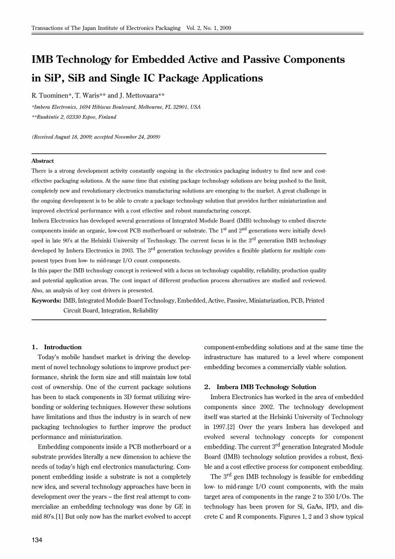
crete C and R components. Figures 1, 2 and 3 show typical
135
IMB module level products with one embedded silicon
component. iQFN represents a low pin-count product area
with only one conductor layer, iBGA has a higher routing
capability through multiple conductor layers, and the stan-
dard IMB module has one embedded component inside a
standard interposer and one wire bonded component on
top (with over-mould). The iQFN package has one conduc-
tor layer that is used for both die to package electrical
interconnection and solder lands. The layer has good level
of freedom to support typical interconnection structures,
and can replicate a standard QFN solder-land layout. The
iBGA package has full freedom in solder-land design and
supports, for example, a full array BGA layout structure.
Requirements for the standard IMB module are similar to
typical interposers and both the upper and lower surfaces
support normal package designs. Furthermore, all module
structures support multiple embedded components that
can be assembled side-by-side or stacked.
IMB technology production utilizes standard, widely
available materials and processes. This enables a large
supply base and competitive total cost of ownership.
The IMB manufacturing process is presented in Figure
4. The process begins with a metal foil onto which
microvias and alignment marks are drilled with a laser.
Non-conductive paste (NCP) is printed onto the foil and
passive and/or active components are assembled using a
chip shooter or flip chip bonder. A minimum of 3 μm copper
or gold metallization is required on the component pad
openings. Typically the components are assembled with a
chip shooter due to its faster processing time, which helps
to minimize the cost of embedding. After the components
are assembled and the NCP is cured, the PCB core is man-
ufactured around the components using standard pre-preg
materials. The pre-preg has pre-manufactured openings in
the area of the embedded components. Material can then
be selected based upon the product requirements (normal
FR-4, high Tg FR-4, or BT epoxy). Once the pre-preg is
cured with a PCB pressing machine, the copper foil is pat-
terned to form the desired routing layer. Several PCB pro-
cess flows can then be selected based upon the product
requirements. In the motherboard applications, the manu-
facturing is typically done using a minimum 50 μm L/S
process. With more advanced structures - such as iBGA -
a semi-additive process can be used to achieve a 30 μm L/S
process or below. In substrate applications the maximum
layer count is normally limited to 6 in order to secure high
yields. A typical layer count in motherboard applications is
from 8 to 10.[3, 4]
Fig. 1 iQFN for sub 100 I/Os.
Fig. 2 iBGA for sub 350 I/Os.
Fig. 3 Standard IMB module for sub 350 I/Os.
Fig. 4 Integrated Module Board process flow (4-layer sub-strate with embedded active and passive).
Fig. 5 Embedded die interconnection area (polymer layersselectively removed).
Tuominen et al.: IMB Technology for Embedded Active and Passive Components (2/5)
136
Transactions of The Japan Institute of Electronics Packaging Vol. 2, No. 1, 2009
Figure 5 presents a top view of the embedded die after
the polymer layers have been selectively removed. The I/O
structure is staggered to several rows in order to provide
sufficient tolerance for the chip shooter machine and PCB
processes.
3. IMB Application AreasIMB application areas are presented in Table 1. The
technology can be utilized in both motherboard and
module types of products. For low-cost packaging the com-
ponent module contains routing layers only on one side of
the module.
The technology provides a flexible and robust platform
for various component types. The technology does not
have any thickness restrictions and can be used with stan-
dard discrete passives, IPD, Si, and GaAs components.
The embedded core is typically less than 250 μm in thick-
ness, with component thicknesses from 50 μm to 150 μm.
In order to fabricate a reliable 3rd generation IMB inter-
connection, the component needs to have a minimum of 3
μm copper or gold plating. Future IMB technology will
enable a bumpless interconnection with metallization
thickness below 1 μm.
4. Reliability EvaluationAn iQFN product with one conductor layer was selected
to verify the IMB technology reliability. The package has
one wiring layer connecting the component I/Os to the
package pins (28 pieces), and a standard QFN solder pad
layout for external connection. The pad pitch is 0.5 mm
and OSP coating covers the pad areas. The package design
enables very good manufacturability and high yields in
manufacturing. Industry standard reliability specifications
were used to determinate the package and board level reli-
ability. The test methods used are shown in Table 2.
The tested package has a 2.13 mm × 2.13 mm daisy-
chain test silicon die embedded inside a 4.0 mm × 4.0 mm
package. The embedded component thickness is 150 μm
and the full package thickness is 340 μm. A 50 μm/50 μm
L/S PCB process was selected for manufacturing the inter-
connection layer. The component was assembled with a
chip shooter machine; ± 13 μm alignment accuracy, 7000
UPH. The final electrical yield of the product was 99.35%.
Figure 6 presents a cross sectional schematic presenta-
tion of the iQFN package structure. The package has one
embedded component and one conductor layer. The same
conductor layer forms the electrical interconnection with
the embedded component and with the motherboard.
A summary of the reliability tests is presented in Table
2. Typical JEDEC standards used in consumer electronics
were selected to verify the reliability of the iQFN package.
Both package and board level tests were selected to
Table 1 IMB application categories.
System in Board (SIB) System in Package (SIP) Low Cost Package
Des
crip
tion
Embedded components inside aPCB motherboard.
» miniaturization» excellent electrical performance
Embedded component inside acomponent interposer.
» miniaturization» excellent electrical performance» excellent themal performance» embedded EMI shield
Escape routing only on one side ofthe package [structure resembles FC-BGA or fan out WLP]
» One or more embeddedcomponents with the package (bothactive and passive).
Feat
ures
High speed component assembly» UPH typically 15000 or higher(only with chip shooter)
Motherboard PCB processes» minimum L/S 50 μm/50 μm» maximum layer count 10
Medium speed component assembly» Chip shooter UPH typically around5000 (down to ± 13 μm accuracy)» FC process user for higher accuracyalignment (UPH below 1000)
Substrate PCB processes» minimum L/S 30 μm/30 μm» maximum layer count 8
Low cost package solution» minimized PCB costs/unit
Medium speed component assembly
Motherboard or substrate PCBprocess
» maximum layer count 3
Em
bedd
edco
mpo
nent
s Medium low I/O count Si or GaAs» up to 150–200 I/Os
Embedded passives;» resistors, capacitors, IPDs
Medium high I/O count Si or GaAs» up to 300–350 I/Os
Embedded passives;» resistors, capacitors, IPDs
Low to medium I/O count Si or GaAs» iQFN around 100 I/Os» iBGA around 300 I/Os
Embedded passives;» resistors, capacitors, IPDs

137
ensure full coverage of potential failure mechanics in dif-
ferent environments. The iQFN package passed all the
tests with no failures.
5. Cost Impact of Assembly and Bumping Technol-ogies
Component assembly cycle time has a crucial role in the
total cost of IMB production. Therefore, it has been impor-
tant for Imbera to develop a fast component-attachment
method to enable wider technology acceptance. These
advanced mass-production methods improve the compo-
nent-assembly process and replace traditional high-accu-
racy Flip-Chip assembly technology in the low-end and
mid-range product areas.
An iBGA design with two conductor layers was chosen
to demonstrate the cost impact of IMB technology in
different manufacturing environments. The example
design is a 7 × 7 mm2 iBGA package with one build-up
layer. The package includes 5 × 5 mm2 silicon component
with 120 I/Os. A schematic diagram of the iBGA package
is shown in Figure 7.
The three different attachment methods in this cost
analysis use Flip Chip, chip shooter, and advanced chip
shooter manufacturing techniques. The chip shooter has a
capacity of 7000 UPH and the advanced chip shooter has a
capacity of 15000 UPH, while the Flip-Chip bonder has a
capacity of below 1000 UPH. The cost impact of the dif-
ferent chip attachment methods are presented in Table 3.
iBGA assembled using the Flip-Chip bonder is indexed to
be 100%. The cost of the alternative bonding technologies
is presented relative to the iBGA assembled using the Flip-
Chip bonder. Shorter assembly time significantly reduces
the total cost of component embedding due to lower
amounts of allocated depreciation and factory overheads.
Also, the improved capacity significantly impacts the
required facility and equipment investment needs.
In the assembly cost comparison, it can be noted that, by
assembling the components with a chip shooter, the cost
efficiency of IMB products can be improved by 20%. By
optimizing the assembly process even further, costs can be
reduced by 25% compared to iBGA products assembled
with a Flip-Chip bonder.
Bumping of the embedded components is also an impor-
tant cost factor. The bump is usually manufactured at the
wafer level and the process includes several steps to form
the desired metallization structure. Imbera 3rd gen IMB
technology utilizes standard Au or Cu bumping techniques
to manufacture an IMB-optimized bump structure. While
Table 2 iQFN test summary
Testmethod
Standard(JEDEC)
Conditions Result
Pack
age
Leve
l
ReflowMoistureSensitibe
J-ST D-020 Level 185°C/85% RH 168 h+ reflow 3 times
pass
ThermalCycling
JES D22-A104 Condition: M (–40°C– + 150°C)Soak mode 3 (10 min)Cycles per hour. 2Cycle count: 500
pass
TemperatureHumidityBiss
JES D22-A101 Condition: 85°C85% humid, 1000 h
pass
High TempStorage
JES D22-A103 Condition A: 125°C,500 h
pass
Low TempStorage
JES D22-A103 Condition A: –40°C ±3°C, 168 h
pass
Boa
rd L
evel
MechanicalShook
JES D22-B104 B, 1500 G pass
ThermalCycling
JES D22-A104 Condition: (–40°C –+125°C)Soak mode 3 (10 min)Cycles per houre. 2Cycle count: 500
pass
Fig. 6 iQFN package structure.
Fig. 7 iBGA package structure.
Table 3 Cost comparison of different component assemblytechnologies.
Tuominen et al.: IMB Technology for Embedded Active and Passive Components (4/5)
138
Transactions of The Japan Institute of Electronics Packaging Vol. 2, No. 1, 2009
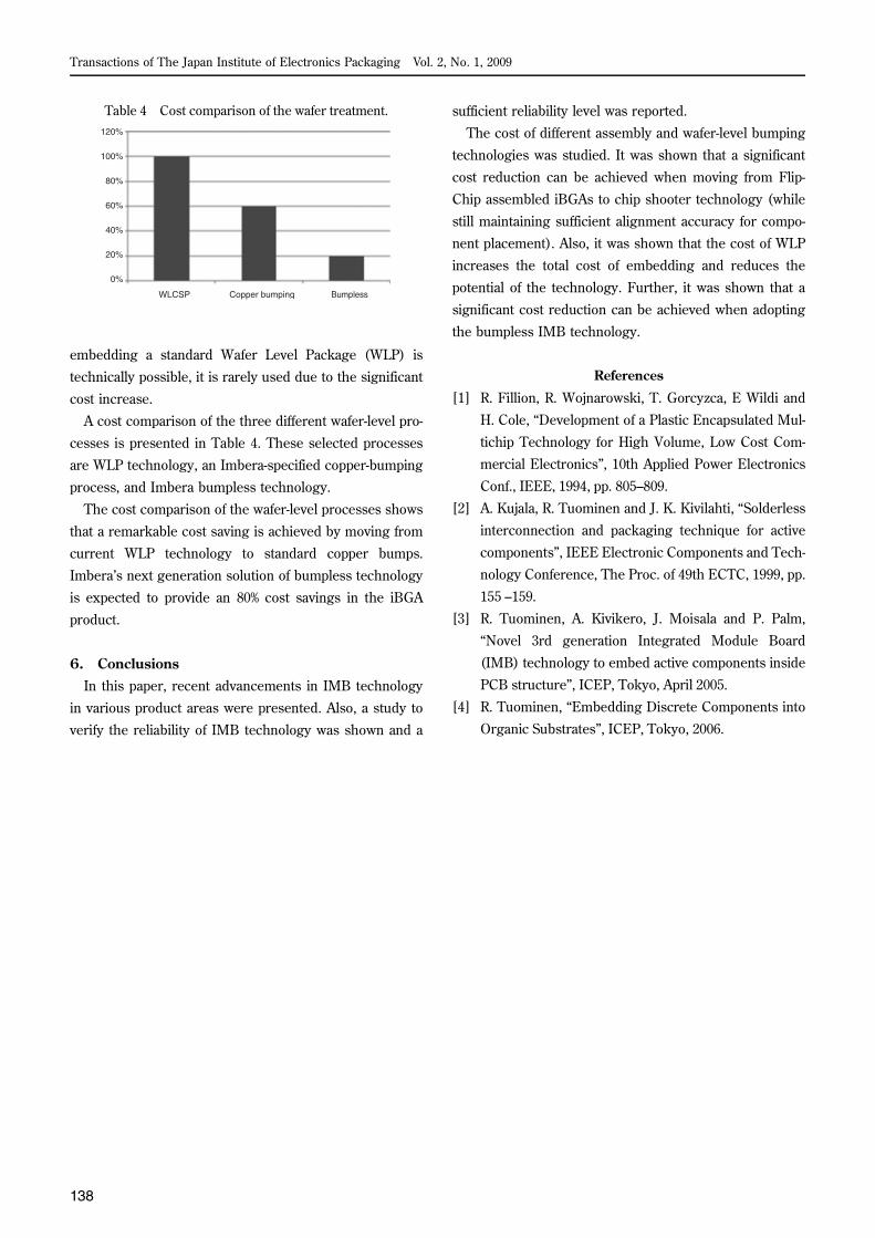
embedding a standard Wafer Level Package (WLP) is
technically possible, it is rarely used due to the significant
cost increase.
A cost comparison of the three different wafer-level pro-
cesses is presented in Table 4. These selected processes
are WLP technology, an Imbera-specified copper-bumping
process, and Imbera bumpless technology.
The cost comparison of the wafer-level processes shows
that a remarkable cost saving is achieved by moving from
current WLP technology to standard copper bumps.
Imbera’s next generation solution of bumpless technology
is expected to provide an 80% cost savings in the iBGA
product.
6. ConclusionsIn this paper, recent advancements in IMB technology
in various product areas were presented. Also, a study to
verify the reliability of IMB technology was shown and a
sufficient reliability level was reported.
The cost of different assembly and wafer-level bumping
technologies was studied. It was shown that a significant
cost reduction can be achieved when moving from Flip-
Chip assembled iBGAs to chip shooter technology (while
still maintaining sufficient alignment accuracy for compo-
nent placement). Also, it was shown that the cost of WLP
increases the total cost of embedding and reduces the
potential of the technology. Further, it was shown that a
significant cost reduction can be achieved when adopting
the bumpless IMB technology.
References
[1] R. Fillion, R. Wojnarowski, T. Gorcyzca, E Wildi and
H. Cole, “Development of a Plastic Encapsulated Mul-
tichip Technology for High Volume, Low Cost Com-
mercial Electronics”, 10th Applied Power Electronics
Conf., IEEE, 1994, pp. 805–809.
[2] A. Kujala, R. Tuominen and J. K. Kivilahti, “Solderless
interconnection and packaging technique for active
components”, IEEE Electronic Components and Tech-
nology Conference, The Proc. of 49th ECTC, 1999, pp.
155 –159.
[3] R. Tuominen, A. Kivikero, J. Moisala and P. Palm,
“Novel 3rd generation Integrated Module Board
(IMB) technology to embed active components inside
PCB structure”, ICEP, Tokyo, April 2005.
[4] R. Tuominen, “Embedding Discrete Components into
Organic Substrates”, ICEP, Tokyo, 2006.
Table 4 Cost comparison of the wafer treatment.