iii-v/si photonics by die-to-wafer bondingphotonics.intec.ugent.be/download/pub_2142.pdf ·...
TRANSCRIPT
ISSN:1369 7021 © Elsevier Ltd 2007JULY-AUGUST 2007 | VOLUME 10 | NUMBER 7-836
III-V/Si photonics by die-to-wafer bonding
Photonics is acknowledged as an enabling technology for the
21st century. It is generally defined as the science in which the
properties of light and its interaction with materials are studied.
Research in the field of integrated photonics is driven by the
advantages seen in integrating electronic functions on electronic
integrated circuits, which are ubiquitously used today. Analogous
to electronic integrated circuits, integrating photonic functions on
a single chip allows the realization of cheaper and more compact
optical systems with higher performance.
Si photonicsSi is the material from which nearly all classical electronic integrated
circuits are fabricated. While SOI is nowadays used for the fabrication
of high-end electronic integrated circuits, the use of the material for
photonic applications is being intensively studied1-5. An SOI wafer
(commercially available up to 300 mm in diameter) consists of a Si
layer on top of a buried SiO2 layer, fabricated on a Si substrate. While
in electronic integrated circuits the presence of the buried SiO2 layer
improves transistor performance, in photonic applications it is used
to create a high vertical refractive index contrast between the Si top
layer (nSi = 3.45) and the SiO2 (nSiO2 = 1.45), that is able to guide
near-infrared light (λ >1.1 μm) in the Si top layer by total internal
reflection. A large omnidirectional index contrast can be obtained
by laterally etching the Si top layer to obtain a Si photonic wire
surrounded by low refractive index air and SiO2 cladding material. In
order to restrain the propagation of light in the optical waveguide to a
Photonic integrated circuits offer the potential of realizing low-cost, compact optical functions. Silicon-on-insulator (SOI) is a promising material platform for this photonic integration, as one can rely on the massive electronics processing infrastructure to process the optical components. However, the integration of a Si laser is hampered by its indirect bandgap. Here, we present the integration of a direct bandgap III-V epitaxial layer on top of the SOI waveguide layer by means of a die-to-wafer bonding process in order to realize near-infrared laser emission on and coupled to SOI.
G. Roelkens1*, J. Van Campenhout1, J. Brouckaert1, D. Van Thourhout1, R. Baets1, P. Rojo Romeo2, P. Regreny2, A. Kazmierczak2,
C. Seassal2, X. Letartre2, G. Hollinger2, J.M. Fedeli3, L. Di Cioccio3, and C. Lagahe-Blanchard4
1Photonics Research Group – UGent/IMEC, Sint-Pietersnieuwstraat 41, B-9000 Ghent, Belgium2Institut des Nanotechnologies de Lyon, Ecole Centrale de Lyon, 36 Avenue Guy de Collongue, 69134 Ecully, France3CEA-DRT/LETI, 17 Rue des Martyrs, 38054 Grenoble Cedex 9, France4TRACIT Technologies, Zone Astec, 15 rue des Martyrs, 38054 Grenoble Cedex 9, France
*E-mail: [email protected]
MT1007_p36_43.indd 36MT1007_p36_43.indd 36 06/06/2007 15:08:1406/06/2007 15:08:14

JULY-AUGUST 2007 | VOLUME 10 | NUMBER 7-8 37
single optical mode at the telecommunication wavelengths of 1.3 μm
and 1.55 μm, a typical maximum waveguide cross-section of 0.1 μm2
is required.
The high omnidirectional refractive index contrast enables the
large-scale integration of optical functions on an SOI chip, as light is
tightly confined to the Si wire. It allows the fabrication of ultracompact
resonators with high quality factor6, wavelength-scale waveguide
bends7, and optical circuits with photonic wire pitches on the order
of 1 μm with negligible crosstalk. Moreover, the tight confinement
and associated high power densities in the photonic wire allow the
nonlinear optical properties of Si to be exploited at moderate optical
power levels. To fabricate these photonic integrated circuits, standard
complementary metal oxide semiconductor (CMOS) technology can
be used. This allows high-yield fabrication and a reduction of the
component cost through economies of scale. Even the integration of
photonic and electronic functions on a common substrate is feasible8.
Although in recent years many research groups have reported high-
performance operation of photonic circuits in SOI (both passive optical
functions like wavelength-selective optical functions3,5-7, optical
power splitters9, and active optical functions like optical modulators10
and all-optical wavelength converters11), the use of Si as a medium
for stimulated light emission has been hampered by its indirect
bandgap. Because of this indirect bandgap, the probability for an
excited electron-hole pair to recombine and emit a photon is strongly
reduced as a result of the much higher nonradiative recombination
rate. Although advances are being made to achieve light emission from
Si, either by modifying the Si on a nanoscale12 or by exploiting its
nonlinear optical properties13, in the foreseeable future these devices
will not outperform their III-V semiconductor counterparts, which
currently supply state-of-the-art opto-electronic components for the
telecommunication market. We, therefore, propose integrating a direct
bandgap III-V layer on top of a SOI waveguide substrate to achieve
stimulated light emission and to couple this stimulated emission to the
underlying SOI waveguide circuit as depicted in Fig. 1. The integration
process should, however, maintain the advantages of the CMOS
manufacturing process, namely the high yield and economy of scale.
Semiconductor wafer bonding There are three main routes to the integration of III-V material on
top of SOI, namely flip-chip integration, heteroepitaxial growth, and
bonding technology. In the first of these, individual laser diode dies
are flip-chipped on and coupled to an SOI waveguide circuit14. While
flip-chip integration is the most rugged, it is a slow and therefore
costly process, as individual dies need to be accurately aligned and
placed on the surface. Also, the integration density is limited by the
pitch and size of the bumps. Heteroepitaxial growth of InP/InGaAsP
– the III-V material used to produce stimulated light emission at the
telecommunication wavelength of 1.55 μm – is hampered by the large
lattice mismatch of 8% between the III-V material and the Si host
substrate. This leads to large threading and misfit dislocation densities
in the grown layers and deterioration of the optical properties.
Although the growth of GaAs (lattice mismatch of 4%) on top of Si
has been demonstrated15, the growth of InP/InGaAsP requires very
thick buffer layers in order to shield the device active layer from the
growth defects16. Advances are being made in heteroepitaxy of AlGaSb
on top of Si because of the fact that the growth mode for AlGaSb is
completely different from that of InP and GaAs17. This might pave the
way for the fabrication of heteroepitaxially grown III-V laser diodes
emitting at telecommunication wavelengths. Temperature budget
and contamination in combination with CMOS electronics fabrication
on the same Si substrate are still an issue, however. The final route,
semiconductor wafer bonding, allows the integration of high-quality
III-V epitaxial layers on top of a Si platform by transferring the III-V
layer stack from its original growth substrate to the SOI wafer. To
decrease the cost of the integration process, in terms of both time
and consumption of expensive III-V material, a die-to-wafer bonding
process has been proposed in which unprocessed InP/InGaAsP dies
are bonded, epitaxial layers down, to the processed SOI wafer. This
reduces material consumption, as III-V semiconductors are only bonded
where they are needed, and reduces the time require to complete
the integration process compared with a flip-chip process, as limited
alignment accuracy is needed because of the absence of structures
on the dies. After bonding, the InP growth substrate is removed, and
Fig. 1 Schematic of how to achieve light emission on a SOI waveguide circuit by integrating III-V epitaxial layers on top of the waveguide circuit and coupling light from the III-V epitaxial layer to the SOI waveguide layer.
III-V/Si photonics by die-to-wafer bonding REVIEW
MT1007_p36_43.indd 37MT1007_p36_43.indd 37 06/06/2007 15:08:2506/06/2007 15:08:25
JULY-AUGUST 2007 | VOLUME 10 | NUMBER 7-838
laser diodes can be fabricated in the InP/InGaAsP epitaxial layers, using
wafer-scale processing, and lithographically aligned to the underlying
SOI features. The drawback of the approach compared with a flip-
chip process is that an electrical and thermal interface is not directly
established, although this can be achieved during the processing of the
III-V opto-electronic components after bonding. Local integration of
III-V material in micrometer-sized areas requires bonding of larger dies
(for the sake of easy handling) and removal by etching after bonding,
while in heteroepitaxial growth, local III-V material integration can be
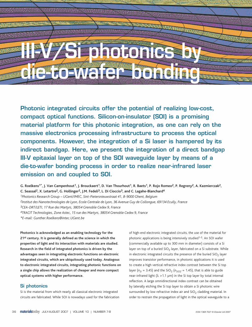
envisioned. The proposed die-to-wafer bonding integration process is
presented in Fig. 2.
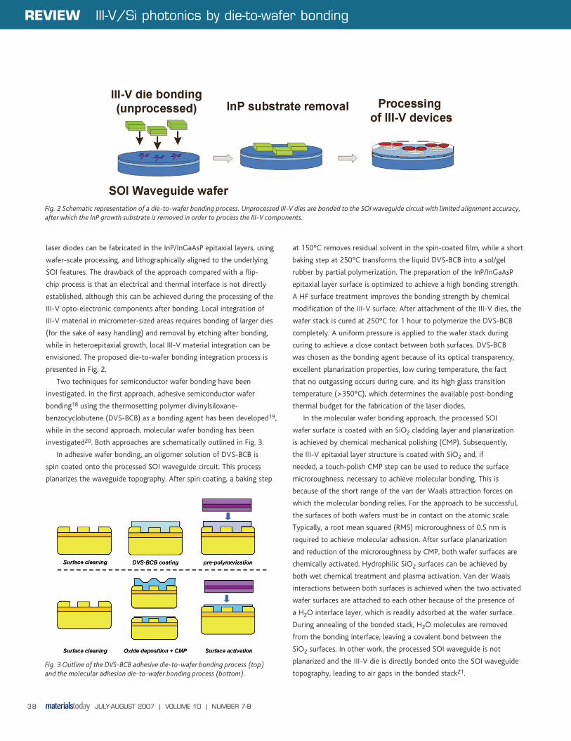
Two techniques for semiconductor wafer bonding have been
investigated. In the first approach, adhesive semiconductor wafer
bonding18 using the thermosetting polymer divinylsiloxane-
benzocyclobutene (DVS-BCB) as a bonding agent has been developed19,
while in the second approach, molecular wafer bonding has been
investigated20. Both approaches are schematically outlined in Fig. 3.
In adhesive wafer bonding, an oligomer solution of DVS-BCB is
spin coated onto the processed SOI waveguide circuit. This process
planarizes the waveguide topography. After spin coating, a baking step
at 150°C removes residual solvent in the spin-coated film, while a short
baking step at 250°C transforms the liquid DVS-BCB into a sol/gel
rubber by partial polymerization. The preparation of the InP/InGaAsP
epitaxial layer surface is optimized to achieve a high bonding strength.
A HF surface treatment improves the bonding strength by chemical
modification of the III-V surface. After attachment of the III-V dies, the
wafer stack is cured at 250°C for 1 hour to polymerize the DVS-BCB
completely. A uniform pressure is applied to the wafer stack during
curing to achieve a close contact between both surfaces. DVS-BCB
was chosen as the bonding agent because of its optical transparency,
excellent planarization properties, low curing temperature, the fact
that no outgassing occurs during cure, and its high glass transition
temperature (>350°C), which determines the available post-bonding
thermal budget for the fabrication of the laser diodes.
In the molecular wafer bonding approach, the processed SOI
wafer surface is coated with an SiO2 cladding layer and planarization
is achieved by chemical mechanical polishing (CMP). Subsequently,
the III-V epitaxial layer structure is coated with SiO2 and, if
needed, a touch-polish CMP step can be used to reduce the surface
microroughness, necessary to achieve molecular bonding. This is
because of the short range of the van der Waals attraction forces on
which the molecular bonding relies. For the approach to be successful,
the surfaces of both wafers must be in contact on the atomic scale.
Typically, a root mean squared (RMS) microroughness of 0.5 nm is
required to achieve molecular adhesion. After surface planarization
and reduction of the microroughness by CMP, both wafer surfaces are
chemically activated. Hydrophilic SiO2 surfaces can be achieved by
both wet chemical treatment and plasma activation. Van der Waals
interactions between both surfaces is achieved when the two activated
wafer surfaces are attached to each other because of the presence of
a H2O interface layer, which is readily adsorbed at the wafer surface.
During annealing of the bonded stack, H2O molecules are removed
from the bonding interface, leaving a covalent bond between the
SiO2 surfaces. In other work, the processed SOI waveguide is not
planarized and the III-V die is directly bonded onto the SOI waveguide
topography, leading to air gaps in the bonded stack21. Fig. 3 Outline of the DVS-BCB adhesive die-to-wafer bonding process (top) and the molecular adhesion die-to-wafer bonding process (bottom).
Fig. 2 Schematic representation of a die-to-wafer bonding process. Unprocessed III-V dies are bonded to the SOI waveguide circuit with limited alignment accuracy, after which the InP growth substrate is removed in order to process the III-V components.
REVIEW III-V/Si photonics by die-to-wafer bonding
MT1007_p36_43.indd 38MT1007_p36_43.indd 38 06/06/2007 15:08:2906/06/2007 15:08:29
JULY-AUGUST 2007 | VOLUME 10 | NUMBER 7-8 39
Although semiconductor wafer bonding is performed in a cleanroom
environment, special care has to be taken to avoid the inclusion of
particles at the bonding interface as they can create large unbonded
areas. Typically, a particle with a height h trapped at the bonding
interface results in a circular unbonded area with a radius of about
5000h20.
After bonding of the III-V dies to the SOI waveguide wafer, the
InP growth substrate is removed using a combination of mechanical
grinding and wet chemical etching using 3HCl:H2O until an InGaAs
etch stop layer is reached. After substrate removal, the bonded
epitaxial layer stack is ready for device processing. An example of an
InP/InGaAsP epitaxial film transferred to an SOI waveguide circuit using
DVS-BCB is shown in Fig. 4.
Laser diodes on SOIThe choice of the architecture of the laser diode and the coupling
method between the III-V layer and the SOI waveguide circuit depends
on the envisaged application. For example, in a transceiver application
for fiber-to-the-home (FTTH)22, high optical output power (milliwatt
range) would be required for the upstream data traffic from the
customers’ home, while the power consumption and footprint of the
laser diode is of minor importance. In this case, the SOI waveguide
circuit would perform the duplexing function of the upstream and
downstream data traffic (at different optical wavelengths). In an
intrachip optical interconnect application23, where laser diodes are used
to transmit data between various points on an electronic integrated
circuit, power consumption and device footprint are of paramount
importance, while optical output power can be fairly low (tens of
microwatts). In this case, the SOI passive waveguide circuit would
only provide the optical point-to-point or broadcasting links on the
electronic integrated circuit. Bearing this application diversity in mind,
two types of laser diode architectures and coupling schemes have been
designed and fabricated. A bonded Fabry-Perot laser diode, injecting
high optical power (milliwatt range) into an SOI waveguide circuit
at the expense of the device footprint and power consumption, and
an ultracompact microdisk laser showing low laser threshold at the
expense of lower output power are characterized below.
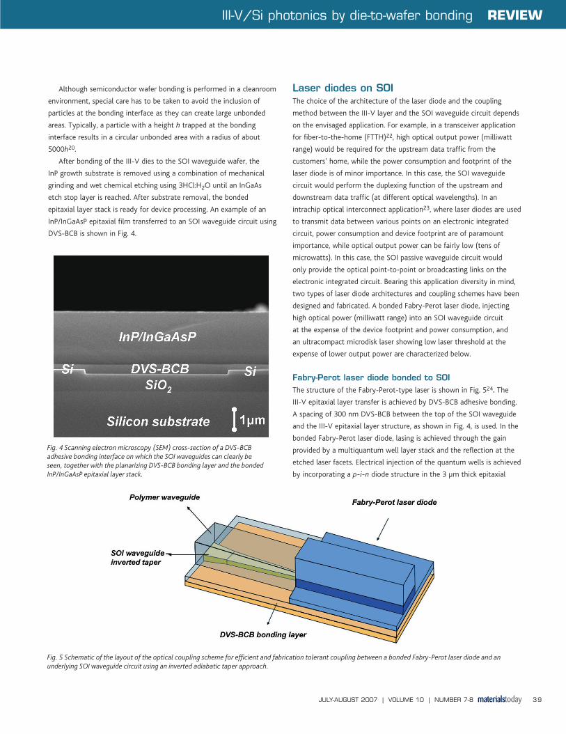
Fabry-Perot laser diode bonded to SOIThe structure of the Fabry-Perot-type laser is shown in Fig. 524. The
III-V epitaxial layer transfer is achieved by DVS-BCB adhesive bonding.
A spacing of 300 nm DVS-BCB between the top of the SOI waveguide
and the III-V epitaxial layer structure, as shown in Fig. 4, is used. In the
bonded Fabry-Perot laser diode, lasing is achieved through the gain
provided by a multiquantum well layer stack and the reflection at the
etched laser facets. Electrical injection of the quantum wells is achieved
by incorporating a p-i-n diode structure in the 3 μm thick epitaxial
Fig. 4 Scanning electron microscopy (SEM) cross-section of a DVS-BCB adhesive bonding interface on which the SOI waveguides can clearly be seen, together with the planarizing DVS-BCB bonding layer and the bonded InP/InGaAsP epitaxial layer stack.
Fig. 5 Schematic of the layout of the optical coupling scheme for efficient and fabrication tolerant coupling between a bonded Fabry-Perot laser diode and an underlying SOI waveguide circuit using an inverted adiabatic taper approach.
III-V/Si photonics by die-to-wafer bonding REVIEW
MT1007_p36_43.indd 39MT1007_p36_43.indd 39 06/06/2007 15:08:3006/06/2007 15:08:30
JULY-AUGUST 2007 | VOLUME 10 | NUMBER 7-840
layer stack and placing the quantum wells in the intrinsic region of the
diode structure. As the stimulated emission exits the edge of the laser
diode, an additional coupling structure is required for efficient coupling
of this stimulated emission to the SOI waveguide. While various
approaches have been investigated, our research has indicated that
an adiabatic inverted taper design is the optimal coupling structure
in terms of coupling efficiency and fabrication tolerance. The concept
of the inverted adiabatic structure is to butt-couple the bonded
laser diode to a polymer waveguide, after which the optical mode is
gradually transformed into that of the SOI waveguide by increasing the
cross-sectional area of the Si wire. The inverted taper tip width has to
be sufficiently small in order for the fundamental optical waveguide
mode at the tip to resemble the waveguide mode of the polymer
waveguide closely. A typical photonic wire cross-sectional area of
0.04 μm2 is required, which is about the limit of what can be achieved
using standard 248 nm deep ultraviolet (UV) CMOS processing
technology for the SOI layer structure used. Gradually broadening the
cross-section of the Si photonic wire increases the pull of light toward
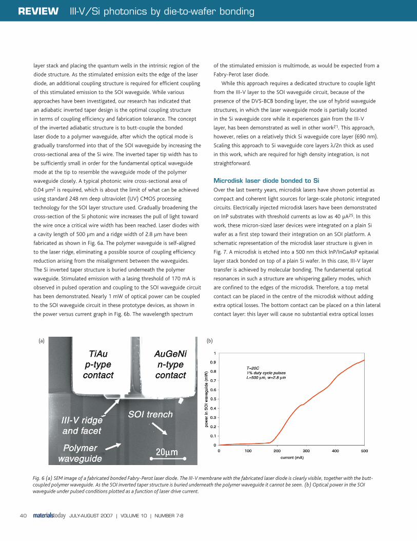
the wire once a critical wire width has been reached. Laser diodes with
a cavity length of 500 μm and a ridge width of 2.8 μm have been
fabricated as shown in Fig. 6a. The polymer waveguide is self-aligned
to the laser ridge, eliminating a possible source of coupling efficiency
reduction arising from the misalignment between the waveguides.
The Si inverted taper structure is buried underneath the polymer
waveguide. Stimulated emission with a lasing threshold of 170 mA is
observed in pulsed operation and coupling to the SOI waveguide circuit
has been demonstrated. Nearly 1 mW of optical power can be coupled
to the SOI waveguide circuit in these prototype devices, as shown in
the power versus current graph in Fig. 6b. The wavelength spectrum
of the stimulated emission is multimode, as would be expected from a
Fabry-Perot laser diode.
While this approach requires a dedicated structure to couple light
from the III-V layer to the SOI waveguide circuit, because of the
presence of the DVS-BCB bonding layer, the use of hybrid waveguide
structures, in which the laser waveguide mode is partially located
in the Si waveguide core while it experiences gain from the III-V
layer, has been demonstrated as well in other work21. This approach,
however, relies on a relatively thick Si waveguide core layer (690 nm).
Scaling this approach to Si waveguide core layers λ/2n thick as used
in this work, which are required for high density integration, is not
straightforward.
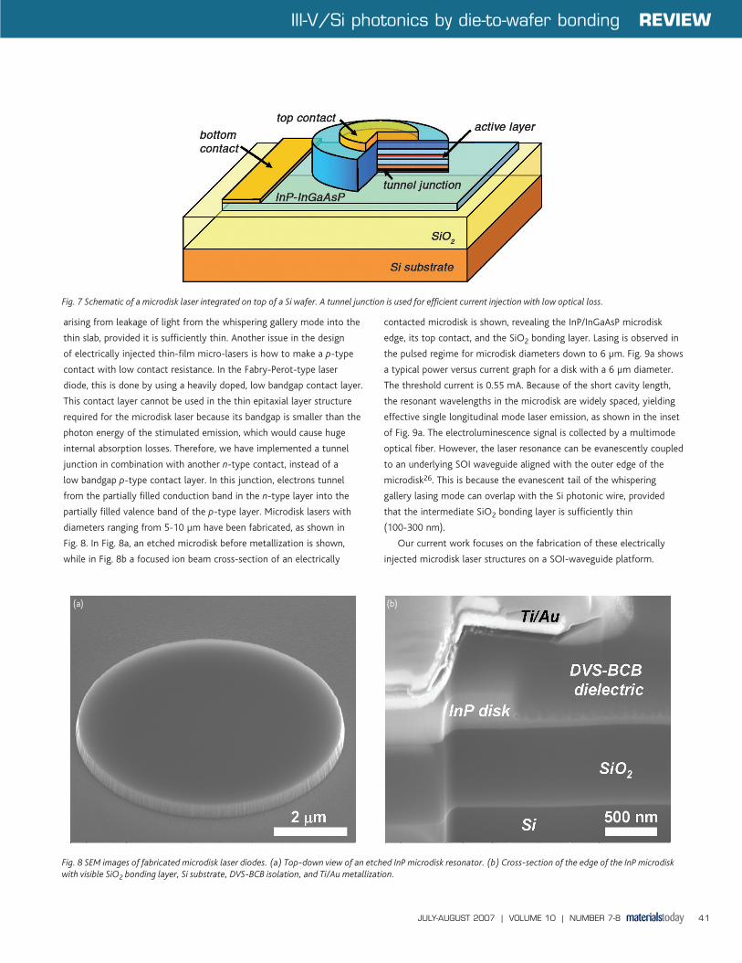
Microdisk laser diode bonded to SiOver the last twenty years, microdisk lasers have shown potential as
compact and coherent light sources for large-scale photonic integrated
circuits. Electrically injected microdisk lasers have been demonstrated
on InP substrates with threshold currents as low as 40 μA25. In this
work, these micron-sized laser devices were integrated on a plain Si
wafer as a first step toward their integration on an SOI platform. A
schematic representation of the microdisk laser structure is given in
Fig. 7. A microdisk is etched into a 500 nm thick InP/InGaAsP epitaxial
layer stack bonded on top of a plain Si wafer. In this case, III-V layer
transfer is achieved by molecular bonding. The fundamental optical
resonances in such a structure are whispering gallery modes, which
are confined to the edges of the microdisk. Therefore, a top metal
contact can be placed in the centre of the microdisk without adding
extra optical losses. The bottom contact can be placed on a thin lateral
contact layer: this layer will cause no substantial extra optical losses
Fig. 6 (a) SEM image of a fabricated bonded Fabry-Perot laser diode. The III-V membrane with the fabricated laser diode is clearly visible, together with the butt-coupled polymer waveguide. As the SOI inverted taper structure is buried underneath the polymer waveguide it cannot be seen. (b) Optical power in the SOI waveguide under pulsed conditions plotted as a function of laser drive current.
REVIEW III-V/Si photonics by die-to-wafer bonding
(b)(a)
MT1007_p36_43.indd 40MT1007_p36_43.indd 40 06/06/2007 15:08:3106/06/2007 15:08:31
JULY-AUGUST 2007 | VOLUME 10 | NUMBER 7-8 41
arising from leakage of light from the whispering gallery mode into the
thin slab, provided it is sufficiently thin. Another issue in the design
of electrically injected thin-film micro-lasers is how to make a p-type
contact with low contact resistance. In the Fabry-Perot-type laser
diode, this is done by using a heavily doped, low bandgap contact layer.
This contact layer cannot be used in the thin epitaxial layer structure
required for the microdisk laser because its bandgap is smaller than the
photon energy of the stimulated emission, which would cause huge
internal absorption losses. Therefore, we have implemented a tunnel
junction in combination with another n-type contact, instead of a
low bandgap p-type contact layer. In this junction, electrons tunnel
from the partially filled conduction band in the n-type layer into the
partially filled valence band of the p-type layer. Microdisk lasers with
diameters ranging from 5-10 μm have been fabricated, as shown in
Fig. 8. In Fig. 8a, an etched microdisk before metallization is shown,
while in Fig. 8b a focused ion beam cross-section of an electrically
contacted microdisk is shown, revealing the InP/InGaAsP microdisk
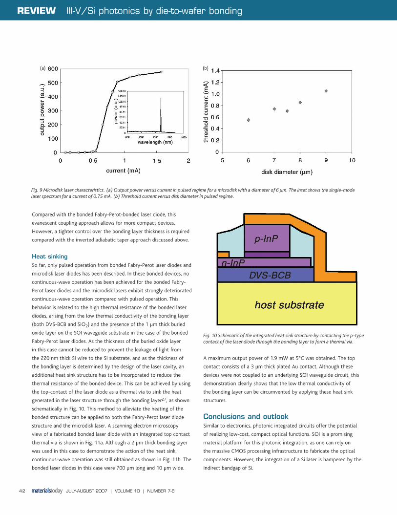
edge, its top contact, and the SiO2 bonding layer. Lasing is observed in
the pulsed regime for microdisk diameters down to 6 μm. Fig. 9a shows
a typical power versus current graph for a disk with a 6 μm diameter.
The threshold current is 0.55 mA. Because of the short cavity length,
the resonant wavelengths in the microdisk are widely spaced, yielding
effective single longitudinal mode laser emission, as shown in the inset
of Fig. 9a. The electroluminescence signal is collected by a multimode
optical fiber. However, the laser resonance can be evanescently coupled
to an underlying SOI waveguide aligned with the outer edge of the
microdisk26. This is because the evanescent tail of the whispering
gallery lasing mode can overlap with the Si photonic wire, provided
that the intermediate SiO2 bonding layer is sufficiently thin
(100-300 nm).
Our current work focuses on the fabrication of these electrically
injected microdisk laser structures on a SOI-waveguide platform.
Fig. 7 Schematic of a microdisk laser integrated on top of a Si wafer. A tunnel junction is used for efficient current injection with low optical loss.
Fig. 8 SEM images of fabricated microdisk laser diodes. (a) Top-down view of an etched InP microdisk resonator. (b) Cross-section of the edge of the InP microdisk with visible SiO2 bonding layer, Si substrate, DVS-BCB isolation, and Ti/Au metallization.
III-V/Si photonics by die-to-wafer bonding REVIEW
(b)(a)
MT1007_p36_43.indd 41MT1007_p36_43.indd 41 06/06/2007 15:08:3606/06/2007 15:08:36
JULY-AUGUST 2007 | VOLUME 10 | NUMBER 7-842
Compared with the bonded Fabry-Perot-bonded laser diode, this
evanescent coupling approach allows for more compact devices.
However, a tighter control over the bonding layer thickness is required
compared with the inverted adiabatic taper approach discussed above.
Heat sinkingSo far, only pulsed operation from bonded Fabry-Perot laser diodes and
microdisk laser diodes has been described. In these bonded devices, no
continuous-wave operation has been achieved for the bonded Fabry-
Perot laser diodes and the microdisk lasers exhibit strongly deteriorated
continuous-wave operation compared with pulsed operation. This
behavior is related to the high thermal resistance of the bonded laser
diodes, arising from the low thermal conductivity of the bonding layer
(both DVS-BCB and SiO2) and the presence of the 1 μm thick buried
oxide layer on the SOI waveguide substrate in the case of the bonded
Fabry-Perot laser diodes. As the thickness of the buried oxide layer
in this case cannot be reduced to prevent the leakage of light from
the 220 nm thick Si wire to the Si substrate, and as the thickness of
the bonding layer is determined by the design of the laser cavity, an
additional heat sink structure has to be incorporated to reduce the
thermal resistance of the bonded device. This can be achieved by using
the top-contact of the laser diode as a thermal via to sink the heat
generated in the laser structure through the bonding layer27, as shown
schematically in Fig. 10. This method to alleviate the heating of the
bonded structure can be applied to both the Fabry-Perot laser diode
structure and the microdisk laser. A scanning electron microscopy
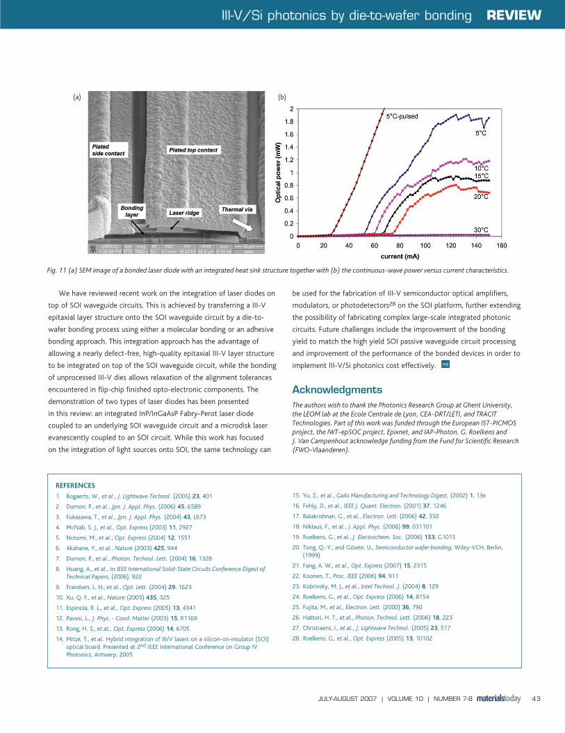
view of a fabricated bonded laser diode with an integrated top contact
thermal via is shown in Fig. 11a. Although a 2 μm thick bonding layer
was used in this case to demonstrate the action of the heat sink,
continuous-wave operation was still obtained as shown in Fig. 11b. The
bonded laser diodes in this case were 700 μm long and 10 μm wide.
A maximum output power of 1.9 mW at 5°C was obtained. The top
contact consists of a 3 μm thick plated Au contact. Although these
devices were not coupled to an underlying SOI waveguide circuit, this
demonstration clearly shows that the low thermal conductivity of
the bonding layer can be circumvented by applying these heat sink
structures.
Conclusions and outlookSimilar to electronics, photonic integrated circuits offer the potential
of realizing low-cost, compact optical functions. SOI is a promising
material platform for this photonic integration, as one can rely on
the massive CMOS processing infrastructure to fabricate the optical
components. However, the integration of a Si laser is hampered by the
indirect bandgap of Si.
Fig. 10 Schematic of the integrated heat sink structure by contacting the p-type contact of the laser diode through the bonding layer to form a thermal via.
Fig. 9 Microdisk laser characteristics. (a) Output power versus current in pulsed regime for a microdisk with a diameter of 6 μm. The inset shows the single-mode laser spectrum for a current of 0.75 mA. (b) Threshold current versus disk diameter in pulsed regime.
REVIEW III-V/Si photonics by die-to-wafer bonding
(b)(a)
MT1007_p36_43.indd 42MT1007_p36_43.indd 42 06/06/2007 15:08:3906/06/2007 15:08:39
JULY-AUGUST 2007 | VOLUME 10 | NUMBER 7-8 43
We have reviewed recent work on the integration of laser diodes on
top of SOI waveguide circuits. This is achieved by transferring a III-V
epitaxial layer structure onto the SOI waveguide circuit by a die-to-
wafer bonding process using either a molecular bonding or an adhesive
bonding approach. This integration approach has the advantage of
allowing a nearly defect-free, high-quality epitaxial III-V layer structure
to be integrated on top of the SOI waveguide circuit, while the bonding
of unprocessed III-V dies allows relaxation of the alignment tolerances
encountered in flip-chip finished opto-electronic components. The
demonstration of two types of laser diodes has been presented
in this review: an integrated InP/InGaAsP Fabry-Perot laser diode
coupled to an underlying SOI waveguide circuit and a microdisk laser
evanescently coupled to an SOI circuit. While this work has focused
on the integration of light sources onto SOI, the same technology can
be used for the fabrication of III-V semiconductor optical amplifiers,
modulators, or photodetectors28 on the SOI platform, further extending
the possibility of fabricating complex large-scale integrated photonic
circuits. Future challenges include the improvement of the bonding
yield to match the high yield SOI passive waveguide circuit processing
and improvement of the performance of the bonded devices in order to
implement III-V/Si photonics cost effectively.
AcknowledgmentsThe authors wish to thank the Photonics Research Group at Ghent University, the LEOM lab at the Ecole Centrale de Lyon, CEA-DRT/LETI, and TRACIT Technologies. Part of this work was funded through the European IST-PICMOS project, the IWT-epSOC project, Epixnet, and IAP-Photon. G. Roelkens and J. Van Campenhout acknowledge funding from the Fund for Scientific Research (FWO-Vlaanderen).
REFERENCES
1. Bogaerts, W., et al., J. Lightwave Technol. (2005) 23, 401
2. Dumon, P., et al., Jpn. J. Appl. Phys. (2006) 45, 6589
3. Fukazawa, T., et al., Jpn. J. Appl. Phys. (2004) 43, L673
4. McNab, S. J., et al., Opt. Express (2003) 11, 2927
5. Notomi, M., et al., Opt. Express (2004) 12, 1551
6. Akahane, Y., et al., Nature (2003) 425, 944
7. Dumon, P., et al., Photon. Technol. Lett. (2004) 16, 1328
8. Huang, A., et al., In IEEE International Solid-State Circuits Conference Digest of Technical Papers, (2006), 922
9. Frandsen, L. H., et al., Opt. Lett. (2004) 29, 1623
10. Xu, Q. F., et al., Nature (2005) 435, 325
11. Espinola, R. L., et al., Opt. Express (2005) 13, 4341
12. Pavesi, L., J. Phys. - Cond. Matter (2003) 15, R1169
13. Rong, H. S., et al., Opt. Express (2006) 14, 6705
14. Mitze, T., et al. Hybrid integration of III/V lasers on a silicon-on-insulator (SOI) optical board. Presented at 2nd IEEE International Conference on Group IV Photonics, Antwerp, 2005
15. Yu, Z., et al., GaAs Manufacturing and Technology Digest, (2002) 1, 13e
16. Fehly, D., et al., IEEE J. Quant. Electron. (2001) 37, 1246
17. Balakrishnan, G., et al., Electron. Lett. (2006) 42, 350
18. Niklaus, F., et al., J. Appl. Phys. (2006) 99, 031101
19. Roelkens, G., et al., J. Electrochem. Soc. (2006) 153, G1015
20. Tong, Q.-Y., and Gösele, U., Semiconductor wafer bonding, Wiley-VCH, Berlin, (1999)
21. Fang, A. W., et al., Opt. Express (2007) 15, 2315
22. Koonen, T., Proc. IEEE (2006) 94, 911
23. Kobrinsky, M. J., et al., Intel Technol. J. (2004) 8, 129
24. Roelkens, G., et al., Opt. Express (2006) 14, 8154
25. Fujita, M., et al., Electron. Lett. (2000) 36, 790
26. Hattori, H. T., et al., Photon. Technol. Lett. (2006) 18, 223
27. Christiaens, I., et al., J. Lightwave Technol. (2005) 23, 517
28. Roelkens, G., et al., Opt. Express (2005) 13, 10102
Fig. 11 (a) SEM image of a bonded laser diode with an integrated heat sink structure together with (b) the continuous-wave power versus current characteristics.
III-V/Si photonics by die-to-wafer bonding REVIEW
(b)(a)
MT1007_p36_43.indd 43MT1007_p36_43.indd 43 06/06/2007 15:08:3906/06/2007 15:08:39