iii-v hbt modeling with hicum - tu dresden hbt modeling with hicum ... • • similar to agilent...
TRANSCRIPT

III-V HBT modeling with HICUM
III-V HBT modeling with HICUM
T. Nardmann, P. Sakalas, M. Schröter Chair for Electron Devices and Integr. Circuits
Univ. of Technol. Dresden, Germany
[email protected], [email protected]://www.iee.et.tu-dresden.de/iee/eb/eb_homee.html
HICUM WorkshopBordeaux, June 28/29, 2011
© 1

III-V HBT modeling with HICUM
OUTLINE
1 Introduction
2 Compact modeling
3 InGaAs/InP technology
4 InGaP/GaAs technology
5 Conclusions
© 2

III-V HBT modeling with HICUM Introduction
Introduction
III-V HBT technology• GaAs HBTs dominate PA handset market
• InP HBTs are among fastest transistors built (record for fT, fmax)
• InP HBTs are suitable for high-speed electronics and optoelectronics applications
• Integration of InP HBTs with silicon appears possible
... however ...• compact models mostly based on external extensions of SGP model due to its
availability in all circuit simulators (incl. special microwave simulators)
• single device parameter extraction => discrete models (vs. scalable in silicon) => no circuit optimization through simple device sizing
• no efficient statistical modeling possible although more needed than for silicon tech-nologies
© 3

III-V HBT modeling with HICUM Introduction
Important physical effects ... in III-V HBTs
• current blocking and charge storage due to conduction band spikes
• collector-base capacitance variation due to III-V electron velocity profile
• velocity overshoot and/or negative differential mobility in low-current transit time
• thermionic emission and tunneling (dep. on composition grading in BE junction)
... and in advanced HBTs in general• collector-base depletion capacitance punch-through
• self-heating
• impact ionization
• NQS effects for charge and transfer current with bias dep. NQS time constants
• bias dependent GICCR weight factors (for graded composition profiles)
=> not covered by (built-in) SGP model
© 4

III-V HBT modeling with HICUM Compact modeling
Compact modelingTypical III-V HBT example: UCSD HBT model
• http://hbt.ucsd.edu/• similar to Agilent AHBT model• self-heating• charge storage in heterojunction• BC capacitance punch-through• neg. diff. mobility (NDM) in τf and CBC
• Missing Effects:• NQS effects• bias-dependent VER
• no scaling available• thermionic emission, tunneling
• Issues• Discrepancy between small-signal and large-signal values: small-signal charge is obtained
by taking τ*Icf, instead of integral over the term• often: III-V HBT models are used only for small-signal modeling• often: proprietary models
=> unavailable across simulators, non-uniform and unreliable implementation
© 5

III-V HBT modeling with HICUM Compact modeling
Physical effects in compact models
physical effect UCSD HICUM/L2 HICUM/L0current blocking and related charge storagein HICUM: for BC junction in GaAsSb/Inp HBT
√ - -
current dependent BC depletion capacit. √ - -
velocity overshoot / negative diff. mobility √ - -
thermionic emission, intraband tunneling - - -
BC depletion capacitance punch-through √ √ √
self-heating √ √ √
impact ionization √ √ √
NQS effects - √ -
bias and bandgap dependent Early effect(relevant only for graded composition)
- √ √
© 6

III-V HBT modeling with HICUM Compact modeling
Goal
Extend Si-based standard model to III-V HBTs
Benefits• Unified standard model => large knowledge pool for parameter extraction methods
• available in all mainstream circuit simulators
• III-V models incapable of modeling Si
• Experience with standardized extraction schemes
• Test structure development experience
=> Establish comprehensive model suitable for all bipolar technologies(possibly model hierarchy)
© 7

III-V HBT modeling with HICUM Compact modeling
Starting point: HICUM/L0 v1.3
• Effects included• self-heating• BC capacitance punch-through• bias-dependent VER
• impact ionization
• Missing • NDM-caused changes in charge
and transit time• NQS effects• current blocking at BE junction,
explicit BC barrier effect
iTB
E
CC’
B’
E’
dQjEdt
--------------
dQjCi*
dt----------------
dQdEdt
----------------
dQdCdt
----------------iAVL rCxijBC
ijBE
rBdQjCx
*
dt------------------
rE
CBEpar
CBCpar
P
Rth
Cth
TjD
• applied to InP HBTs
• no special test structures available for geometry scaling => single device extraction necessay
© 8
III-V HBT modeling with HICUM Compact modeling
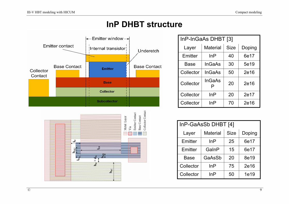
InP DHBT structureInP-InGaAs DHBT [3]
Layer Material Size Doping
Emitter InP 40 6e17
Base InGaAs 30 5e19
Collector InGaAs 50 2e16
Collector InGaAsP 20 2e16
Collector InP 20 2e17
Collector InP 70 2e16
InP-GaAsSb DHBT [4]Layer Material Size Doping
Emitter InP 25 6e17
Emitter GaInP 15 6e17
Base GaAsSb 20 8e19
Collector InP 75 2e16
Collector InP 50 1e19
© 9

III-V HBT modeling with HICUM Compact modeling
Band diagrams of DHBTs
InP-InGaAs DHBT band diagram at forward active bias (from [3])
type I vs type II BC band diagramat zero and forward bias (from [5])
=> GaAsSb base is more attractive approach
© 10

III-V HBT modeling with HICUM InGaAs/InP technology
InGaAs/InP technology• Transistors provided by Fraunhofer IAF
• fT ≈ 350 GHz, fmax ≈ 400 GHz
• HICUM/L0 version 1.3 used [2] • physical formulation for bias dependent VER (relevant for compositional grading)• temperature dependence of VER
• no test structures or scaling, automated extraction with manual improvement• calculation of series resistances from theory and sheet resistance• measurements at various ambient temperatures available for extraction of temperature
related parameters
• for more information see CSICS 2011 [6]
© 11

III-V HBT modeling with HICUM InGaAs/InP technology
Experimental resultsGummel characteristics at different VBC
0.5 0.6 0.7 0.8 0.9 1
10−5
100
VBE
(V)
J (m
A/μ
m2)
VBC = -0.25 V
0.5 0.6 0.7 0.8 0.9 1
10−6
10−4
10−2
100
VBE
(V)
J (m
A/μ
m2 )
VBC = 0 V
0.5 0.6 0.7 0.8 0.9 1
10−5
100
VBE
(V)
J (m
A/μ
m2)
VBC = 0.5 V
© 12

III-V HBT modeling with HICUM InGaAs/InP technology
Experimental results output characteristics transit frequency VBC
0 0.5 1 1.50
1
2
3
4
5
VCE
(V)
J C (
mA
/μm
2 )
10−1
1000
100
200
300
400
JC (mA/μm2)
f T (
GH
z)VBE = [0.74, 0.8, 0.86, 0.88, 0.9, 0.92] V VBC = [-0.25, -0.1, 0, 0.3, 0.5] V
=> very good agreement
© 13

III-V HBT modeling with HICUM InGaAs/InP technology
Experimental results max. available power gain power added efficiency
100
1015
10
15
20
25
30
35
freq (GHz)
MAG
(dB)
−35 −25 −15 −50
10
20
30
Pin
(dBm)
Gai
n (d
B)
−35 −25 −15 −50
10
20
30
PAE
(%)
JC = 2 mA/µm², VBC = -0.1 V (≈ 2/3 ft,peak)
JC = {0.5, 2.0} and {1.0, 3.8} mA/µm², VBC = {0.3, 0}V (1/2 ft,peak, ft,peak)
=> already acceptable agreement
© 14

III-V HBT modeling with HICUM InGaP/GaAs technology
InGaP/GaAs technology
• DHBTs provided by Skyworks Inc.
• fT ≈ 45...60 GHz, fmax ≈ 80...95 GHz
• three different base widths were investigated: wB = {50, 70, 90} nm
• Focus on noise sources
• for more information see PSS 2011 [7]
© 15

III-V HBT modeling with HICUM InGaP/GaAs technology
Experimental results Gummel characteristics transit frequency
VBC = 0 V
VBC = 0 V
=> deviations at medium JCpossibly caused by missing
velocity overshoot
=> good agreement
© 16
III-V HBT modeling with HICUM InGaP/GaAs technology
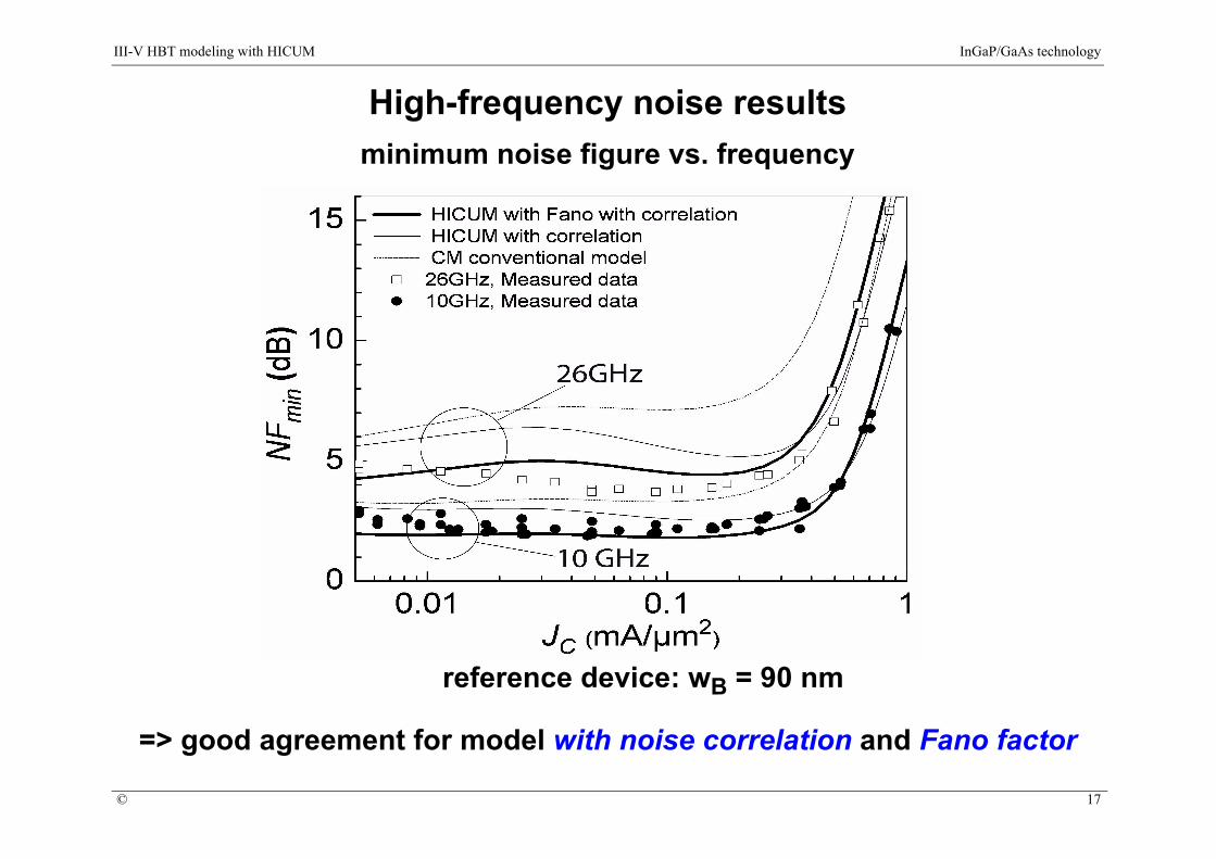
High-frequency noise resultsminimum noise figure vs. frequency
reference device: wB = 90 nm
VBC = 0 V
=> good agreement for model with noise correlation and Fano factor
© 17

III-V HBT modeling with HICUM Conclusions
Conclusions
• successfully applied HICUM/L0 to InGaAs/InP HBT, HICUM/L2 to InGaP/GaAs HBT• HICUM/L0 required addition of IBC,rec, ajC
• Good results for standard characteristics, large-signal, and noise measurements• deviations in fT at medium current densities for InGaP/GaAs HBT
• planned: addition of III-V (especially InP) specific features related to • carrier transport• charge storage (vel. overshoot/neg. diff. mobility, current-dependent CjC) • device scaling and statistical models
AcknowledgmentsThe authors would like to thank the DFG for financial support. They are also indebted to the Fraunhofer IAF and Skyworks for supplying wafers
© 18

III-V HBT modeling with HICUM References
References[1] http://hbt.ucsd.edu/[2] A. Pawlak, M. Schröter, A. Mukherjee, S. Lehmann, S. Shou, D. Céli, "Automated
Model Complexity Reduction using the HICUM Hierarchy", Proc. IEEE SCD, 4p, 2011.
[3] K. Schneider, “Broadband Amplifiers for High Data Rates using InP/InGaAs Double Heterojunction Bipolar Transistors”, Diss., Universitätsverlag Karlsruhe, 2006.
[4] H. G. Liu, O. Ostinelli, Y. Zend, C. R. Bolognesi, "600 GHz InP/GaAsSb/InP DHBTs Grown by MOCVD with a GaAsSb Graded-Base and fT x BVCEO > 2.5 THz-V at Room Temperature", IEDM Digest, pp. 667-670, 2007.
[5] V. Nodjiadjim et al, "Comparative collector design in InGaAs and GaAsSb based InP DHBTs", Proc. IRPM, pp. 1-4, 2008.
[6] M. Schroter, A. Pawlak, P. Sakalas, J. Krause, T. Nardmann, "SiGeC and InP HBT compact modeling for mm-wave and THz applications", inv. paper at CSICS 2011.
[7] A. Shimukovitch, P. Sakalas, P. Zampardi, M. Schröter and A. Matulionis "Investi-gation of electron delay in the base on noise performance in InGaP heterojunction bipolar transistors" Phys. Status Solidi, No. 11, pp. 335–337, 2010.
© 19