ieee transactions on very large scale...
TRANSCRIPT

IEEE TRANSACTIONS ON VERY LARGE SCALE INTEGRATION (VLSI) SYSTEMS, VOL. 17, NO. 4, APRIL 2009 473
Fault Secure Encoder and Decoder forNanoMemory Applications
Helia Naeimi and André DeHon
Abstract—Memory cells have been protected from soft errors formore than a decade; due to the increase in soft error rate in logiccircuits, the encoder and decoder circuitry around the memoryblocks have become susceptible to soft errors as well and mustalso be protected. We introduce a new approach to design fault-se-cure encoder and decoder circuitry for memory designs. The keynovel contribution of this paper is identifying and defining a newclass of error-correcting codes whose redundancy makes the de-sign of fault-secure detectors (FSD) particularly simple. We fur-ther quantify the importance of protecting encoder and decodercircuitry against transient errors, illustrating a scenario where thesystem failure rate (FIT) is dominated by the failure rate of the en-coder and decoder. We prove that Euclidean Geometry Low-Den-sity Parity-Check (EG-LDPC) codes have the fault-secure detectorcapability. Using some of the smaller EG-LDPC codes, we can tol-erate bit or nanowire defect rates of 10% and fault rates of �� ��
upsets/device/cycle, achieving a FIT rate at or below one for theentire memory system and a memory density of ���� bit/cm� withnanowire pitch of 10 nm for memory blocks of 10 Mb or larger.Larger EG-LDPC codes can achieve even higher reliability andlower area overhead.
Index Terms—Decoder, encoder, fault tolerant, memory, nan-otechnology.
I. INTRODUCTION AND MOTIVATION
N ANOTECHNOLOGY provides smaller, faster, and lowerenergy devices which allow more powerful and com-
pact circuitry; however, these benefits come with a cost—thenanoscale devices may be less reliable. Thermal- and shot-noiseestimations [8], [12] alone suggest that the transient fault rateof an individual nanoscale device (e.g., transistor or nanowire)may be orders of magnitude higher than today’s devices. As aresult, we can expect combinational logic to be susceptible totransient faults in addition to storage cells and communicationchannels. Therefore, the paradigm of protecting only memorycells and assuming the surrounding circuitries (i.e., encoderand decoder) will never introduce errors is no longer valid.
Manuscript received January 29, 2008; revised July 14, 2008. First publishedFebruary 27, 2009; current version published March 18, 2009. This researchwas supported in part by National Science Foundation Grant CCF-0403674and by the Defense Advanced Research Projects Agency under ONR ContractN00014-01-0651.
H. Naeimi was with the Computer Science Department, California Institute ofTechnology, Pasadena, CA 91125 USA. She is now with Intel Research, SantaClara Laboratory, Santa Clara, CA 95054 USA (e-mail: [email protected]).
A. DeHon is with the Department of Electrical and Systems Engineering,University of Pennsylvania, Philadelphia, PA 19104 USA (e-mail: [email protected]).
Digital Object Identifier 10.1109/TVLSI.2008.2009217
In this paper, we introduce a fault-tolerant nanoscale memoryarchitecture which tolerates transient faults both in the storageunit and in the supporting logic (i.e., encoder, decoder (cor-rector), and detector circuitries).
Particularly, we identify a class of error-correcting codes(ECCs) that guarantees the existence of a simple fault-tolerantdetector design. This class satisfies a new, restricted definitionfor ECCs which guarantees that the ECC codeword has an ap-propriate redundancy structure such that it can detect multipleerrors occurring in both the stored codeword in memory andthe surrounding circuitries. We call this type of error-correctingcodes, fault-secure detector capable ECCs (FSD-ECC). Theparity-check Matrix of an FSD-ECC has a particular structurethat the decoder circuit, generated from the parity-check Ma-trix, is Fault-Secure. The ECCs we identify in this class areclose to optimal in rate and distance, suggesting we can achievethis property without sacrificing traditional ECC metrics.
We use the fault-secure detection unit to design a fault-tol-erant encoder and corrector by monitoring their outputs. If a de-tector detects an error in either of these units, that unit must re-peat the operation to generate the correct output vector. Usingthis retry technique, we can correct potential transient errors inthe encoder and corrector outputs and provide a fully fault-tol-erant memory system.
The novel contributions of this paper include the following:1) a mathematical definition of ECCs which have simple
FSD which do not requiring the addition of further redun-dancies in order to achieve the fault-secure property (seeSection IV);
2) identification and proof that an existing LDPC code (EG-LDPC) has the FSD property (see Section V);
3) a detailed ECC encoder, decoder, and corrector design thatcan be built out of fault-prone circuits when protected bythis fault-secure detector also implemented in fault-pronecircuits and guarded with a simple OR gate built out ofreliable circuitry (see Section VI).
To further show the practical viability of these codes, we workthrough the engineering design of a nanoscale memory systembased on these encoders and decoders including the following:
• memory banking strategies and scrubbing (seeSection VI-E);
• reliability analysis (see Section VII);• unified ECC scheme for both permanent memory bit de-
fects and transient upsets (see Section VIII).This allows us to report the area, performance, and reliabilityachieved for systems based on these encoders and decoders(see Section IX). We start by reviewing the related work (seeSection II) to put this development in context, and we provide
1063-8210/$25.00 © 2009 IEEE
Authorized licensed use limited to: CALIFORNIA INSTITUTE OF TECHNOLOGY. Downloaded on April 13, 2009 at 17:27 from IEEE Xplore. Restrictions apply.
474 IEEE TRANSACTIONS ON VERY LARGE SCALE INTEGRATION (VLSI) SYSTEMS, VOL. 17, NO. 4, APRIL 2009
an overview of the system architecture for the fault-tolerantmemory system (see Section III) which uses these circuits.
We first introduced the concept of ECC with fault-secure de-tector in [19]; then we developed the nanowire-based imple-mentation and memory-system optimization in [20]. In additionto combining the results from our earlier papers, this paper de-scribes how to use the single ECC system for both permanentdefect and transient fault tolerance. This article also provides amore detailed accounting of net memory bit density.
II. RELATED WORK
Traditionally, memory cells were the only circuitry suscep-tible to transient faults, and all the supporting circuitries aroundthe memory (i.e., encoders and decoders) were assumed to befault-free. As a result most of prior work designs for fault-tol-erant memory systems focused on protecting only the memorycells. However, as we continue scaling down feature sizes oruse sublithographic devices, the surrounding circuitries of thememory system will also be susceptible to permanent defectsand transient faults [11].
One approach to avoid the reliability problem in the sur-rounding circuitries is to implement these units with morereliable devices (e.g., more reliable CMOS technologies [6],[26]). However, from an area, performance, and power con-sumption point of view it is beneficial to implement encodersand decoders with scaled feature size or nanotechnology de-vices. Consequently, it is important to remove the reliabilitybarrier for these logic circuits so they can be implemented withscaled feature size or nanotechnology devices.
Almost all of the proposed fault tolerant encoders and de-coders so far, use the conventional fault tolerant scheme (e.g.,logic replication or concurrent parity prediction) to protect theencoder and corrector circuitry. That is, they add additionallogic to check the correctness of the circuit calculation. In con-trast, the technique introduced in this work exploits the existingstructure of the ECC to guarantee the fault-secure property ofthe detector unit without adding redundant computations.
The work presented in [21], is an example of the scheme usingredundancy to generate fault tolerant encoder. Reference [21]develops a fault-secure encoder unit using a concurrent parity-prediction scheme. Like the general parity-prediction technique,[21] concurrently generates (predicts) the parity-bits of the en-coder outputs (encoded bits) from the encoder inputs (informa-tion bits). The predicted parity bits are then compared againstthe actual parity function of the encoder output (encoded bits)to check the correctness of the encoder unit. The parity pre-dictor circuit implementation is further optimized for each ECCto make a more compact design. For this reason, efficient parity-prediction designs are tailored to a specific code. Simple parityprediction guarantees single error detection; however, no gen-eralization is given for detecting multiple errors in the detectorother than complete replication of the prediction and compar-ison units.
In contrast, our design detects multiple errors in the encoderand corrector units. Furthermore, the fault-secure detector andchecking logic for our FSD-ECC codes can be automaticallygenerated from the already known parity-check matrix. This
fault secure detector delivers protection without requiring ad-ditional fault-tolerance circuitry.
III. SYSTEM OVERVIEW
In this section, we outline our memory system design that cantolerate errors in any part of the system, including the storageunit and encoder and corrector circuits using the fault-securedetector. For a particular ECC used for memory protection, let
be the maximum number of error bits that the code can correctand be the maximum number of error bits that it can detect,and in one error combination that strikes the system, let , ,and be the number of errors in encoder, a memory word,and corrector, and let and be the number of errors inthe two separate detectors monitoring the encoder and correctorunits. In conventional designs, the system would guarantee errorcorrection as long as and . In contrast, herewe guarantee that the system can correct any error combinationas long as , , and
. This design is feasible when the following two fundamentalproperties are satisfied:
1) any single error in the encoder or corrector circuitry can atmost corrupt a single codeword bit (i.e., no single error canpropagate to multiple codeword bits);
2) there is a fault secure detector that can detect any combi-nation of errors in the received codeword along with errorsin the detector circuit. This fault-secure detector can verifythe correctness of the encoder and corrector operation.
The first property is easily satisfied by preventing logic sharingbetween the circuits producing each codeword bit or infor-mation bit in the encoder and the corrector respectively. InSection IV, we define the requirements for a code to satisfy thesecond property.
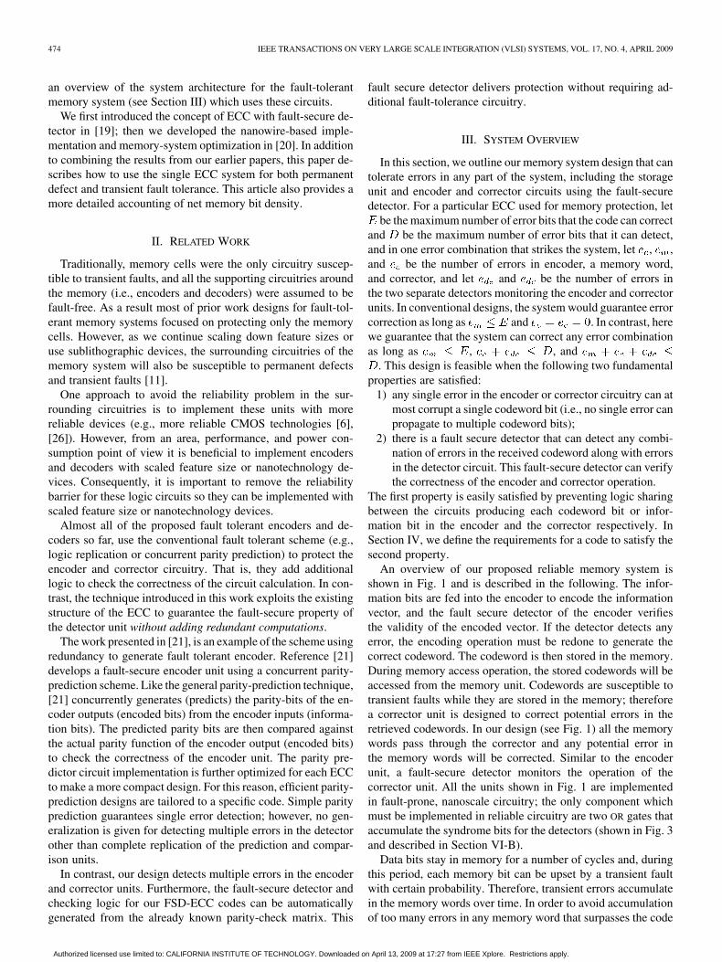
An overview of our proposed reliable memory system isshown in Fig. 1 and is described in the following. The infor-mation bits are fed into the encoder to encode the informationvector, and the fault secure detector of the encoder verifiesthe validity of the encoded vector. If the detector detects anyerror, the encoding operation must be redone to generate thecorrect codeword. The codeword is then stored in the memory.During memory access operation, the stored codewords will beaccessed from the memory unit. Codewords are susceptible totransient faults while they are stored in the memory; thereforea corrector unit is designed to correct potential errors in theretrieved codewords. In our design (see Fig. 1) all the memorywords pass through the corrector and any potential error inthe memory words will be corrected. Similar to the encoderunit, a fault-secure detector monitors the operation of thecorrector unit. All the units shown in Fig. 1 are implementedin fault-prone, nanoscale circuitry; the only component whichmust be implemented in reliable circuitry are two OR gates thataccumulate the syndrome bits for the detectors (shown in Fig. 3and described in Section VI-B).
Data bits stay in memory for a number of cycles and, duringthis period, each memory bit can be upset by a transient faultwith certain probability. Therefore, transient errors accumulatein the memory words over time. In order to avoid accumulationof too many errors in any memory word that surpasses the code
Authorized licensed use limited to: CALIFORNIA INSTITUTE OF TECHNOLOGY. Downloaded on April 13, 2009 at 17:27 from IEEE Xplore. Restrictions apply.

NAEIMI AND DEHON: FAULT SECURE ENCODER AND DECODER FOR NANOMEMORY APPLICATIONS 475
Fig. 1. Overview of our proposed fault-tolerant memory architecture, with pipelined corrector.
correction capability, the system must perform memory scrub-bing. Memory scrubbing is the process of periodically readingmemory words from the memory, correcting any potential er-rors, and writing them back into the memory (e.g., [22]). Thisfeature is shown in the revised system overview in Fig. 10. Toperform the periodic scrubbing operation, the normal memoryaccess operation is stopped and the memory performs the scruboperation. In Section VI, we further detail the scrubbing oper-ation and potential optimization to achieve high performanceand high reliability. We also explain each of the above units, en-coder, corrector, and detector, and memory operations in greaterdetail in Section VI.
IV. ECCS WITH FAULT SECURE DETECTOR
In this section, we present our novel, restricted ECC defini-tion for our fault-secure detector capable codes. Before startingthe details of our new definition we briefly review basic linearECCs.
A. Error-Correcting Code Reviews
Let be the -bit information vector thatwill be encoded into an -bit codeword, .For linear codes, the encoding operation essentially performsthe following vector-matrix multiplication:
(1)
where is a generator matrix. The validity of a receivedencoded vector can be checked with the Parity-Check matrix,which is an binary matrix named . The checkingor detecting operation is basically summarized as the followingvector-matrix multiplication:
(2)
The -bit vector is called the syndrome vector. A syn-drome vector is zero if is a valid codeword, and nonzero if isan erroneous codeword. Each code is uniquely specified by itsgenerator matrix or parity-check matrix.
A code is a systematic code if every codeword consists of theoriginal -bit information vector followed by parity bits[16]. With this definition, the generator matrix of a systematiccode must have the following structure:
(3)
where is a identity matrix and is a matrixthat generates the parity-bits. The advantage of using systematiccodes is that there is no need for a decoder circuit to extract theinformation bits. The information bits are simply available inthe first bits of any encoded vector.
A code is said to be a cyclic code if for any codeword , all thecyclic shifts of the codeword are still valid codewords. A codeis cyclic iff the rows of its parity-check matrix and generatormatrix are the cyclic shifts of their first rows.
The minimum distance of an ECC, , is the minimum numberof code bits that are different between any two codewords. Themaximum number of errors that an ECC can detect is ,and the maximum number that it corrects is . Any ECCis represented with a triple , representing code length,information bit length, and minimum distance, respectively.
B. FSD-ECC Definition
The restricted ECC definition which guarantees a FSD-ECCis as follows.
Definition I: Let be an ECC with minimum distance .is FSD-ECC if it can detect any combination of overallor fewer errors in the received codeword and in the detectorcircuitry.
Theorem I: Let be an ECC, with minimum distance .is FSD-ECC iff any error vector of weight , hassyndrome vector of weight at least .
Note: The following proof depends on the fact that any singleerror in the detector circuitry can corrupt at most one output(one syndrome bit). This can be easily satisfied for any circuitby implementing the circuit in such a way that no logic elementis shared among multiple output bits; therefore, any single errorin the circuit corrupts at most one output (one syndrome bit).
Proof: The core of a detector circuitry is a multiplier thatimplements the vector-matrix multiply of the received vectorand the parity-check matrix to generate the syndrome vector.Now if errors strike the received codeword the syndromeweight of the error pattern is at least from the assumption.Furthermore, the maximum number of tolerable errors in thewhole system is and errors already exist in the encodedvector, therefore the maximum number of errors that can strikein the detector circuitry is . From the previous note,these many errors can corrupt at most syndrome bit,which in worst case leaves at least one nonzero syndrome bitand therefore detects the errors.
The difference between FSD-ECC and normal ECC is simplythe demand on syndrome weight. That is, for error vector ofweight , a normal ECC demands nonzero syndromeweight while FSD-ECC demands syndrome weight of .
Authorized licensed use limited to: CALIFORNIA INSTITUTE OF TECHNOLOGY. Downloaded on April 13, 2009 at 17:27 from IEEE Xplore. Restrictions apply.

476 IEEE TRANSACTIONS ON VERY LARGE SCALE INTEGRATION (VLSI) SYSTEMS, VOL. 17, NO. 4, APRIL 2009
V. FSD-ECC EXAMPLE: EUCLIDEAN GEOMETRY CODES
A. Euclidean Geometry Code Review
This section reviews the construction of Euclidean Geometrycodes based on the lines and points of the corresponding fi-nite geometries [27]. Euclidean Geometry codes are also calledEG-LDPC codes based on the fact that they are low-densityparity-check (LDPC) codes [14]. LDPC codes have a limitednumber of 1’s in each row and column of the matrix; this limitguarantees limited complexity in their associated detectors andcorrectors making them fast and light weight [9].
Let be a Euclidean Geometry with points and lines.is a finite geometry that is shown to have the following
fundamental structural properties:1) every line consists of points;2) any two points are connected by exactly one line;3) every point is intersected by lines;4) two lines intersect in exactly one point or they are parallel;
i.e., they do not intersect.Let be a binary matrix, whose rows and columns
corresponds to lines and points in an Euclidean geometry,respectively, where if and only if the th line ofcontains the th point of , and otherwise. A row in
displays the points on a specific line of and has weight. A column in displays the lines that intersect at a specific
point in and has weight . The rows of are called theincidence vectors of the lines in , and the columns of arecalled the intersecting vectors of the points in . Therefore,
is the incidence matrix of the lines in over the points in. It is shown in [15] that is a LDPC matrix, and therefore
the code is an LDPC code.A special subclass of EG-LDPC codes, type-I 2-D EG-LDPC,
is considered here. It is shown in [15] that type-I 2-D EG-LDPChave the following parameters for any positive integer :
• information bits, ;• length, ;• minimum distance, ;• dimensions of the parity-check matrix, ;• row weight of the parity-check matrix, ;• column weight of the parity-check matrix, .It is important to note that the rows of are not necessarily
linearly independent, and therefore the number of rows do notnecessarily represents the rank of the matrix. The rank ofis which makes the code of this matrix linear code.Since the matrix is , the implementation has syndromebits instead of . The , parity-check ma-trix of an euclidean geometry, can be formed by takingthe incidence vector of a line in and its cyclic shiftsas rows; therefore this code is a cyclic code.
B. FSD-ECC Proof for EG-LDPC
In this section, we prove that EG-LDPC codes have theFSD-ECC property.
Theorem II: Type-I 2-D EG-LDPC codes are FSD-ECC.Proof: Let be an EG-LDPC code with column weight
and minimum distance . We have to show that any error vectorof weight corrupting the received encoded vectorhas syndrome vector of weight at least .
TABLE IEG-LDPCS AND UPPER AND LOWER BOUNDS ON CODE LENGTH
Now a specific bit in the syndrome vector will be one if andonly if the parity-check sum corresponding to this syndromevector has an odd number of error bits present in it. Lookingfrom the Euclidean geometry perspective, each error bit cor-responds to a point in the geometry and each bit in the syn-drome vector corresponds to a line. Consequently, we are in-terested in obtaining a lower bound on the number of lines thatpass through an odd number of error points. We further lowerbound this quantity by the number of lines that pass throughexactly one of the error points. Based on the definition of theEuclidean geometry, lines pass through each point; so errorpoints potentially impact lines. Also at most one line con-nects two points. Therefore, looking at the error points, thereare at most lines between pairs of error points. Hence, thenumber of lines passing through a collection of these pointsis lower bounded by . Out of this number, at mostlines connect two or more points of the error points. Summa-rizing all this, the number of lines passing through exactly oneerror point, which gives us the lower bound on the syndromevector weight, is at least .
From the code properties introduced in Section V-A andknowing that , we can derive the following inequality:
when
The previous inequality says that the weight of the syndromevector of a codeword with errors is at least when
which is the required condition of Theorem (I). Therefore,EG-LDPC is FSD-ECC.
C. Efficiency of EG-LDPC
It is important to compare the rate of the EG-LDPC codewith other codes to understand if the interesting properties oflow-density and FSD-ECC come at the expense of lower coderates. We compare the code rates of the EG-LDPC codes that weuse here with an achievable code rate upper bound (Gilbert-Var-shamov bound) and a lower bound (Hamming bound). Table Ishows the upper and lower bounds on the code overhead, foreach of the used EG-LDPC. The EG-LDPC codes are no largerthan the achievable Gilbert bound for the same and value,and they are not much larger than the Hamming bounds. Conse-quently, we see that we achieve the FSD property without sac-rificing code compactness.
VI. DESIGN STRUCTURE
In this section, we provide the design structure of the en-coder, corrector, and detector units of our proposed fault-tol-erant memory system. We also present the implementation of
Authorized licensed use limited to: CALIFORNIA INSTITUTE OF TECHNOLOGY. Downloaded on April 13, 2009 at 17:27 from IEEE Xplore. Restrictions apply.

NAEIMI AND DEHON: FAULT SECURE ENCODER AND DECODER FOR NANOMEMORY APPLICATIONS 477
Fig. 2. Structure of NanoMemory core. Please note that the address decodersare for memory access and are not related to the memory ECC decoders.
these units on a sub-lithographic, nanowire-based substrate. Be-fore going into the design structure details we start with a briefoverview of the sub-lithographic memory architecture model.
A. NanoMemory Architecture Model
We use the NanoMemory [4], [6] and NanoPLA [5] archi-tectures to implement the memory core and the supportinglogic, respectively. NanoMemory and NanoPLA are based onnanowire crossbars [2], [10].
The NanoMemory architecture developed in [4], [6] canachieve greater than b/cm density even after includingthe lithographic-scale address wires and defects. This designuses a nanowire crossbar to store memory bits and a limitednumber of lithographic scale wires for address and control lines.Fig. 2 shows a schematic overview of this memory structure.The fine crossbar shown in the center of the picture stores onememory bit in each crossbar junction. To be able to write thevalue of each bit into a junction, the two nanowires crossingthat junction must be uniquely selected and an adequate voltagemust be applied to them (e.g., [3], [24]). The nanowires can beuniquely selected through the two address decoders located onthe two sides of the memory core.
The detail of the NanoMemory structure is presented in [4]and [6]. For our design, we revise the original NanoMemorystructure introduced in [4] and [6]. Instead of using a litho-graphic-scale interface to read and write into the memory core,we use a nanowire-based interface. The reason that we can re-move the lithographic-scale interface is that all the blocks inter-facing with the memory core (encoder, corrector and detectors)are implemented with nanowire-based crossbars. So we use ananowire-based DEMUX to connect the memory core to the sup-porting logic blocks. The detail of the DEMUX structure is avail-able in [17], [18], and [20].
B. Fault Secure Detector
The core of the detector operation is to generate the syn-drome vector, which is basically implementing the followingvector-matrix multiplication on the received encoded vectorand parity-check matrix :
(4)
Fig. 3. Fault-secure detector for (15, 7, 5) EG-LDPC code. All the gates exceptthe last OR gate are implemeneted with fault-prone nanoscale circuitry. The lastOR gate is implemented with more reliable lithography technique.
TABLE IIDETECTOR, ENCODER, AND CORRECTOR CIRCUIT AREA IN THE
NUMBER OF 2-INPUT GATES
Therefore each bit of the syndrome vector is the product ofwith one row of the parity-check matrix. This product is a linearbinary sum over digits of where the corresponding digit inthe matrix row is 1. This binary sum is implemented with anXOR gate. Fig. 3 shows the detector circuit for the (15, 7, 5)EG-LDPC code. Since the row weight of the parity-check ma-trix is , to generate one digit of the syndrome vector we needa -input XOR gate, or 2-input XOR gates. For the wholedetector, it takes 2-input XOR gates. Table II illustratesthis quantity for some of the smaller EG-LDPC codes. Note thatimplementing each syndrome bit with a separate XOR gate satis-fies the assumption of Theorem I of no logic sharing in detectorcircuit implementation.
An error is detected if any of the syndrome bits has a nonzerovalue. The final error detection signal is implemented by an OR
function of all the syndrome bits. The output of this -input OR
gate is the error detector signal (see Fig. 3). In order to avoida single point of failure, we must implement the OR gate witha reliable substrate (e.g., in a system with sub-lithographicnanowire substrate, the OR gate is implemented with reliablelithographic technology—i.e., lithographic-scaled wire-OR).This -input wire-OR is much smaller than implementing theentire 2-input XORs at the lithographic scale. Thearea of each detector is computed using the model of NanoPLAand NanoMemory form [5] and [4] and [6] accounting for allthe supporting lithographic wires and reported in Table III.
Fig. 4 shows the implementation of the detector on aNanoPLA substrate. The framed block in Fig. 4(b) showsa -input XOR gate, implementing a -level XOR treein spiral form (see Fig. 4(a)). The solid boxes display therestoration planes and the white boxes display the wired-OR
planes of NanoPLA architecture model [5], [7]. In Fig. 4, thesignals rotate counter clock-wise, and each round of signalgenerates the XOR functions of one level of the XOR-tree. Thefinal output then gates a robust lithographic-scale wire. Thislithographic-scale wire generates a wired-OR function of all the
Authorized licensed use limited to: CALIFORNIA INSTITUTE OF TECHNOLOGY. Downloaded on April 13, 2009 at 17:27 from IEEE Xplore. Restrictions apply.

478 IEEE TRANSACTIONS ON VERY LARGE SCALE INTEGRATION (VLSI) SYSTEMS, VOL. 17, NO. 4, APRIL 2009
TABLE IIIDECOMPOSED AREA PER BIT OF THE DESIGN POINTS SELECTED FOR THE CURVES IN Fig. 14. THE MEMORY SIZE FOR THIS DESIGN IS �� bit. THE UNIT OF
AREA IS NANOMETERS SQUARED PER BIT
Fig. 4. (a) �-input XOR tree implemented on NanoPLA structure. (b) Detector circuit implemented on NanoPLA: The parameters in the figure are � � � � � ,� � �� � ��� � ��, � � � ���� � � �� � �� � ��� � ��, and � � ��� � , where � ���, is the width of a NanoPLA plane with nanowire, includingthe area of the supporting lithographic scale wires.
-input XORs and is the final output of the detector circuit.The XOR gate is the main building block of the encoder andcorrector as well.
C. Encoder
An -bit codeword , which encodes a -bit informationvector is generated by multiplying the -bit informationvector with a bit generator matrix ; i.e., .
EG-LDPC codes are not systematic and the information bitsmust be decoded from the encoded vector, which is not desirablefor our fault-tolerant approach due to the further complicationand delay that it adds to the operation. However, these codes arecyclic codes [15]. We used the procedure presented in [15] and
Fig. 5. Generator matrix for the (15, 7, 5) EG-LDPC in systematic format; notethe identity matrix in the left columns.
[16] to convert the cyclic generator matrices to systematic gen-erator matrices for all the EG-LDPC codes under consideration.
Authorized licensed use limited to: CALIFORNIA INSTITUTE OF TECHNOLOGY. Downloaded on April 13, 2009 at 17:27 from IEEE Xplore. Restrictions apply.

NAEIMI AND DEHON: FAULT SECURE ENCODER AND DECODER FOR NANOMEMORY APPLICATIONS 479
Fig. 6. Structure of an encoder circuit for the (15, 7, 5) EG-LDPC code; � to � are 7-bit information vector. Each of the XOR gates generate one parity bit of theencoded vector. The codeword consists of seven information bits followed by eight parity bits.
Fig. 5 shows the systematic generator matrix to generate (15,7, 5) EG-LDPC code. The encoded vector consists of informa-tion bits followed by parity bits, where each parity bit is simplyan inner product of information vector and a column of , from
. Fig. 6 shows the encoder circuit to computethe parity bits of the (15, 7, 5) EG-LDPC code. In this figure
is the information vector and will be copied tobits of the encoded vector, , and the rest of encoded
vector, the parity bits, are linear sums (XOR) of the informationbits.
If the building block is two-input gates then the encoder cir-cuitry takes 22 two-input XOR gates. Table II shows the area ofthe encoder circuits for each EG-LDPC codes under considera-tion based on their generator matrices.
Once the XOR functions are known, the encoder structure isvery similar to the detector structure shown in Fig. 4, except itconsists of XOR gates of varying numbers of inputs. Eachnanowire-based XOR gate has structure similar to the XOR treeshown in Fig. 4.
D. Corrector
One-step majority-logic correction is a fast and relativelycompact error-correcting technique [15]. There is a limitedclass of ECCs that are one-step-majority correctable whichinclude type-I two-dimensional EG-LDPC. In this section,we present a brief review of this correcting technique. Thenwe show the one-step majority-logic corrector for EG-LDPCcodes.
1) One-Step Majority-Logic Corrector: One-step majority-logic correction is the procedure that identifies the correct valueof a each bit in the codeword directly from the received code-word; this is in contrast to the general message-passing error-correction strategy (e.g., [23]) which may demand multiple iter-ations of error diagnosis and trial correction. Avoiding iterationmakes the correction latency both small and deterministic. Thistechnique can be implemented serially to provide a compact im-plementation or in parallel to minimize correction latency.
This method consists of two parts: 1) generating a specificset of linear sums of the received vector bits and 2) finding themajority value of the computed linear sums. The majority valueindicates the correctness of the code-bit under consideration; ifthe majority value is 1, the bit is inverted, otherwise it is keptunchanged.
The theory behind the one-step majority corrector and theproof that EG-LDPC codes have this property are availablein [15]. Here we overview the structure of such correctors forEG-LDPC codes.
Fig. 7. Serial one-step majority logic corrector structure to correct last bit (bit14th) of 15-bit (15,7,5) EG-LDPC code.
A linear sum of the received encoded vector bits canbe formed by computing the inner product of the receivedvector and a row of a parity-check matrix. This sum is calledParity-Check sum. The core of the one-step majority-logic cor-rector is generating parity-check sums from the appropriaterows of the parity-check matrix. The one-step majority logicerror correction is summarized in the following procedure.These steps correct a potential error in one code bit lets say,e.g., .
1) Generate parity-check sums by computing the innerproduct of the received vector and the appropriate rows ofparity-check matrix.
2) The check sums are fed into a majority gate. The outputof the majority gate corrects the bit by inverting thevalue of if the output of majority gate is “1”.
The circuit implementing a serial one-step majority logic cor-rector for (15, 7, 5) EG-LDPC code is shown in Fig. 7. This cir-cuit generates parity-check sums with XOR gates and thencomputes the majority value of the parity-check sums. Sinceeach parity-check sum is computed using a row of the parity-check matrix and the row density of EG-LDPC codes are , eachXOR gate that computes the linear sum has inputs. The singleXOR gate on the right of Fig. 7 corrects the code bit usingthe output of the majority gate. Once the code bit is cor-rected the codeword is cyclic shifted and code bit is placedat position and will be corrected. The whole codeword canbe corrected in rounds.
If implemented in flat, two-level logic, a majority gate couldtake exponential area. The two-level majority gate is imple-mented by computing all the product terms that have
ON inputs and one -input OR-term. For ex-
ample, the majority of 3 inputs , , is computed withproduct terms and one 3-input OR-terms as follows:
(5)
Authorized licensed use limited to: CALIFORNIA INSTITUTE OF TECHNOLOGY. Downloaded on April 13, 2009 at 17:27 from IEEE Xplore. Restrictions apply.

480 IEEE TRANSACTIONS ON VERY LARGE SCALE INTEGRATION (VLSI) SYSTEMS, VOL. 17, NO. 4, APRIL 2009
Fig. 8. (a) Four-input sorting network; each vertical line shows a one-inputcomparator. (b) One comparator structure.
Fig. 9. Eight-input majority gate using sorting network.
In the next section we presents a novel, compact implementationof majority circuits.
2) Majority Circuit Implementation: Here we present a com-pact implementation for the majority gate using Sorting Net-works [13]. The majority gate has application in many othererror-correcting codes, and this compact implementation canimprove many other applications.
A majority function of binary digits is simply the medianof the digits (where we define the median of an even number ofdigits as the smallest digit).
To find the median of the inputs, we do the following:1) divide the inputs into two halves with size ;2) sort each of the halves;3) the median is 1 if for the th element of
one half and the th element of the other halfare both 1.
We use binary Sorting Networks [13] to do the sort operationof the second step efficiently. An -input sorting network is thestructure that sorts a set of bits, using a 2-bit sorter buildingblocks. Fig. 8(a) shows a 4-input sorting network. Each of thevertical lines represents one comparator which compares twobits and assigns the larger one to the top output and the smallerone to the bottom [see Fig. 8(b)]. The four-input sorting net-work, has five comparator blocks, where each block consists oftwo two-input gates; overall the four-input sorting network con-sists of ten two-input gates in total.
To check the condition in the third step, we use two-inputAND gates followed by a -input OR gate. Fig. 9 shows thecircuit implementing the above technique to find the medianvalue of 8 bits. It has two -input (four-input) sorting net-works followed by combinational circuitry, consisting of fourtwo-input AND gates and a four-input OR gate, which can beimplemented with three two-input OR gates. Therefore in totalan eight-input majority gate implemented with sorting networkstake 27 two-input gates; in contrast, the two-level implementa-tion of this majority gate takes five-input AND gatesand one 56-input OR gate.
3) Serial Corrector: As mentioned earlier, the same one-stepmajority-logic corrector can be used to correct all the bits ofthe received codeword of a cyclic code. To correct each code-bit,the received encoded vector is cyclic shifted and fed into to theXOR gates as shown in Fig. 7. The serial majority corrector takes
Fig. 10. Partial system overview with serial corrector. Here only the correctorand its detector are shown; these blocks connect to the memory block and therest of the system shown in Fig. 1.
cycles to correct an erroneous codeword. If the fault rate islow, the corrector block is used infrequently; since the commoncase is error-free codewords, the latency of the corrector will nothave a severe impact on the average memory read latency. Theserial corrector must be placed off the normal memory read path.This is shown in Fig. 10. The memory words retrieved fromthe memory unit are checked by detector unit. If the detectordetects an error, the memory word is sent to the corrector unitto be corrected, which has the latency of the detector plus theround latency of the corrector.
4) Parallel Corrector: For high error rates [e.g., whentolerating permanent defects in memory words as well (seeSection VIII)], the corrector is used more frequently and itslatency can impact the system performance. Therefore wecan implement a parallel one-step majority corrector whichis essentially copies of the single one-step majority-logiccorrector. Fig. 1 shows a system integration using the parallelcorrector. All the memory words are pipelined through theparallel corrector. This way the corrected memory wordsare generated every cycle. The detector in the parallel casemonitors the operation of the corrector, if the output of thecorrector is erroneous, the detector signals the corrector torepeat the operation. Note that faults detected in a nominallycorrected memory word arise solely from faults in the detectorand corrector circuitry and not from faults in the memoryword. Since detector and corrector circuitry are relatively smallcompared to the memory system, the failure rate of these unitsis relatively low; e.g., in a memory system that runs at 1 GHzand , the parallel corrector for a (255, 175, 17)code should see one upset every 30 hours (calculation is doneusing the reliability equations in Section VII). Therefore, theerror detection and repeat process happens infrequently anddoes not impact the system throughput.
Assuming our building blocks are two-input gates, numberof -input parity-check sums will require two-inputXOR gates. The size of the majority gate is defined by the sortingnetwork implementation. Table II shows the overall area of a se-rial one-step majority-logic corrector in the number of two-inputgates for the codes under consideration. The parallel implemen-tation consists of exactly copies of the serial one-step ma-jority-logic corrector.
Generating the linear binary sums (XORs) of the one-step ma-jority sum is the same as Fig. 4. The majority gate is simplycomputed following the structure shown in Fig. 9 using thenanowire-based substrate.
Authorized licensed use limited to: CALIFORNIA INSTITUTE OF TECHNOLOGY. Downloaded on April 13, 2009 at 17:27 from IEEE Xplore. Restrictions apply.

NAEIMI AND DEHON: FAULT SECURE ENCODER AND DECODER FOR NANOMEMORY APPLICATIONS 481
Fig. 11. Banked memory organization, with single global corrector.
E. Banked Memory
Large memories are conventionally organized as sets ofsmaller memory blocks called banks. The reason for breaking alarge memory into smaller banks is to trade off overall memorydensity for access speed and reliability. Excessively small banksizes will incur a large area overhead for memory drivers andreceivers. Large memory banks require long rows and columnswhich results in high capacitance wires that consequently in-creases the delay. Furthermore long wires are more susceptibleto breaks and bridging defects. Therefore excessively largememory banks have high defect rate and low performance.The organization of NanoMemory is not different from theconventional memory organization, except that the overheadper bank is larger due to the scale difference between the size ofa memory bit (a single wire crossing) and the support structures(e.g., microscale wires for addressing and bootstrapping). Thework presented in [6] provides more detail on memory banksand shows how the banks would be integrated into a completememory system. The memory system overview shown in Fig. 1can be generalized to multiple banks as shown in Fig. 11,where similarly the encoder and correctors are protected withfault-secure detectors.
Memory words must be scrubbed frequently to prevent erroraccumulation. The number of faults that accumulate in thememory is directly related to the scrubbing period. The longerthe scrubbing period is, the larger the number of errors thatcan accumulate in the system. However, scrubbing all memorywords serially can take a long time. If the time to serially scrubthe memory becomes noticeable compared to the scrubbingperiod, it can reduce the system performance. To reduce thescrubbing time, we can potentially scrub all the memory banksin parallel. For this, each memory bank requires a separatecorrector and detector unit. It may not be necessary to go tothe extreme of scrubbing all banks in parallel. Instead, we cancluster a number of memory banks together and consider acorrector and detector unit for each Cluster. Fig. 12 shows amemory system with two parallel corrector units. Here each
Fig. 12. Banked memory organization with cluster size of 2.
cluster contains two memory banks. In Section IX, we calculatethe appropriate cluster sizes to balance performance and area.
VII. RELIABILITY ANALYSIS
In this section, we analyze the reliability of the system. Tomeasure the system reliability, we estimate the probability thatsystem fails—i.e., the system experiences a greater number oferrors in a memory word than the number of errors the error-cor-recting code can tolerate. With this analysis, we then show theimpact of protecting the ECC support logic (see Section VII-B).
A. Analysis
We assume the fault probability of each device at each cyclehas i.i.d. and random distribution over the devices of the
memory system. Recall and are the nominal number of er-rors that occurs in encoder and encoder detector during memorywrite operation at one instance. Similarly, , , and arethe number of errors that occur in a memory word and its corre-sponding corrector and detector. Let , , and be the sizeof the circuitry involved in an operation on a single code bit inthe encoder, corrector, or detector, respectively. This is the sizeof the logic cone of a single output of each of the above units. Forexample, in a detector each logic cone is a -input XOR gate gen-erating a single bit of the syndrome vector (see Section VI-B).
Let a nominal unit have a logic cone size of ( may be oneof the values , , ). With worst-case analysis the outputof the logic cone fails when any of the devices in the logic conefails. So when at least one of the devices inside the cone iserroneous, the output of the logic cone, which is a code bit,would be erroneous. Therefore, the probability that a code bitis erroneous in any of the above units is
. Similarly the probability that a memory-bit is erroneousin scrubbing interval of cycles is
(6)
where is the number of devices contained in one memorycell. When using 6 T-SRAM cells, . When using aNanoMemory, the memory bit is essentially a single nanowire
Authorized licensed use limited to: CALIFORNIA INSTITUTE OF TECHNOLOGY. Downloaded on April 13, 2009 at 17:27 from IEEE Xplore. Restrictions apply.

482 IEEE TRANSACTIONS ON VERY LARGE SCALE INTEGRATION (VLSI) SYSTEMS, VOL. 17, NO. 4, APRIL 2009
crosspoint. However, since accessing each memory bit requiresreading the signal value through a pair of nanowires (see Fig. 2),the correctness of each memory bit depends on the correctnessof two nanowires. Therefore, for the NanoMemory design,
. Each unit or a memory-word experience errors amongbits of the codeword with the probability
(7)
which is simply a binomial distribution; is the code-length,is either or , and is , , , ,
or .As explained in Section VI-B, errors in the encoder unit are
detected by its following detector, and are corrected by repeatingthe encoding operation to generate a correct encoded vector. Thedetector can detect up to errors overall in these two units.Where is the code distance. With worst-case assumptions, thedetector fails to detect the errors if there are more thanerrors. Therefore, we define the first reliability condition as
Cond. I)
which states that the total number of errors in the encoder unitand the following detector unit must be smaller than the min-imum distance of the code. The detector of the corrector isalso capable of detecting up to errors accumulated frommemory unit, corrector unit and the second detector unit. Sim-ilarly with worst-case assumption, the detector fails to detecterrors when they are more than . Therefore, the second re-liability condition is defined as
Cond. II)
Furthermore, the corrector can recover a memory-word with upto errors from the memory unit. If moreerrors are accumulated in a memory word, then the EG-LDPCcodes cannot correct the memory word. Therefore, the third re-liability condition is formulated as
Cond. III)
which states that the maximum number of tolerable errors ineach memory word is . Satisfying the three previous condi-tions guarantees that the memory system operates with no un-detectable or uncorrectable errors. We calculated the probabilityof each of the above conditions employing (7), for all the var-ious EG-LDPC codes.
Section IX illustrates the reliability of the system for differentdevice failure rate . It also presents the best design points foroptimizing reliability, area, and throughput.
B. Impact of Providing Reliability for Supporting Logic
It is important to understand the impact of protecting the sup-porting logic on the system FIT rate. Could the system FIT ratebe low enough if only memory words were protected? What isthe potential cost of protecting the supporting logic? We answerthese questions with the following example.
Fig. 13. Impact of protecting logic on system reliability for fault rate equals�� per bit per cycle �� � �� �.
Fig. 13 shows the FIT rate of the system decomposed into thecontribution from the memory bank and the contribution fromthe supporting logic. The FIT in the supporting logic is withouta fault-secure detector (i.e., any error in the supporting logic re-sults an erroneous output, with worst-case analysis). Obviouslythe FIT of the whole system with no logic protection is the sumof the above two FITs, illustrated with a solid line. This graphis plotted for a device fault rate of with a memoryscrubbing interval of 10 minutes. As you can see, for codes withminimum distance larger than 9, the FIT of the system withno logic protection is dominated by the FIT of the unprotectedlogic. Using codes with greater redundancy will decrease theFIT of memory bank; however, since the unprotected logic hasa nontrivial FIT rate, increasing the code redundancy withoutprotecting the logic does not decrease the FIT of the compositesystem. To achieve the higher reliability the logic must also beprotected. The FIT of such system with fault secure logic is il-lustrated with the dashed line, and as you can see, the FIT ofthis system follows very closely the FIT of the memory bank.Protecting supporting logic, is essentially done by the fault-se-cure detector and the only cost to achieve the logic protectionis the cost that we pay for the detectors. Table III shows thatthe detector takes a negligible fraction of area compared to thememory core, encoder, and corrector. Therefore with minimalarea overhead the system reliability can be greatly improved.
VIII. TOLERATING PERMANENT DEFECT IN MEMORY CELLS
In this paper, so far we focused on a transient fault-tolerantmemory structure. Equally important is to tolerate permanentdefects in the memory systems. Since the memory unit has aregular structure, most of the defect tolerant designs are basedon row and column sparing. This means that we overpopulatethe rows and columns based on the expected defect rate so thatafter removing all the defective rows and columns the memoryhas the desired size. For example, if we want to have a 1 K
1 K memory, and the junction defect rate is 0.001% whichresults in nanowire defect rate of ,then, with 2% row and column overpopulation (20 more rows
Authorized licensed use limited to: CALIFORNIA INSTITUTE OF TECHNOLOGY. Downloaded on April 13, 2009 at 17:27 from IEEE Xplore. Restrictions apply.

NAEIMI AND DEHON: FAULT SECURE ENCODER AND DECODER FOR NANOMEMORY APPLICATIONS 483
and columns), the system yields a 1 K 1 K memory core with99.6% probability
(8)
and the memory yields when both rows and columns yieldwhich is the product of the two probabilities and
(9)
So when the defect rate is small (0.001%), even with very smallarea overhead (2% overpopulation), the system can yield a per-fect 1 K 1 K memory core with high probability.
A. ECC for Defect Tolerance
However, with higher defect rates, the column and rowsparing can be very costly. For example, a 1% junction defectrate on a nanowire with 1000 junctions implies that, with almost100% probability, every nanowire in the memory block has atleast one defective junction. At this defect rate we cannot affordto discard nanowires with any defective junctions. The workpresented in [6] suggests a defect tolerant technique that ismore efficient than the column and row sparing. This techniquediscards nanowires that have more defective junctions thana set threshold. These nanowires will be replaced with sparenanowires. The limited number of defective junctions on theremaining nanowires are tolerated using ECCs.
For the previous example with a junction defect rate of 1%,if we keep nanowires with up to 12 defective junctions, then thesystem would require only 31% row and column overpopulationto achieve 99% yield. The computation is shown as follows. Theprobability that a wire is accepted—i.e., has at most 12 defectivejunction—is
(10)
With only 31% column and row sparing we can get 99% yield
(11)
and the final memory yield is
(12)
In [6], it is suggested that a reliable lithographic-scale encoderand decoder be used to encode and decode memory bits to tol-erate limited defective bits in each row. With the techniques in-troduced here, the encoder and decoder can be built with fault-prone nanowire circuitry as well.
Here we use the same EG-LDPC codes that we use for tran-sient faults for tolerating permanent defects. The error correc-
tion capability of the ECC is partitioned between fault toler-ance and defect tolerance similar to the approach in [26]. Forexample, the EG-LDPC code (255, 175, 17) can correct up toeight errors in each memory word. This can be partitioned totolerate four transient faults and four permanent defect in eachcode word. With this technique we allow each memory word(code word) to contain up to four defective junctions; with a rowwidth of 1020, this is about 16 defective junctions per row sinceeach row holds four memory words and each memory word tol-erates four defects.
This reduces the area overhead compared to solely row andcolumn sparing. The important point is that this area overheadreduction is achieved with almost no extra cost since it uses thestructure which already exists for transient fault tolerance—i.e.,encoder, corrector, and detector units. The only potential draw-back point for this technique is that it increases the effective FITrate of the memory block relative to the case where we had all8 errors available to tolerate transient upsets. Therefore to guar-antee the desired reliability, codes with larger minimum distancewhich can tolerate larger numbers of defects and faults must beused. Section IX shows detail results on how the reliability andarea overhead costs are balanced.
[25] and [26] present more sophisticated schemes for memorydefect tolerance at the cost of reliable, CMOS ECC circuitry andmemories to remap or invert blocks. Our scheme minimizes thereliable support needed for the nanoscale memory.
B. Impact on Error Correction Frequency
When we have a limited number of defective junction inmemory words, this means that with high probability a memoryword has erroneous bits and must be corrected. Therefore,as mentioned in Section III we use a parallel, fully pipelinedcorrector to prevent throughput loss. The probability that amemory word has a limited number of defects is computed inthe following. Remember that the memory words with morethan a set threshold are removed. Let the set threshold of thenumber of defects in each memory word be , and thedefect rate be , therefore the memory words have 0 todefective bits. The probability that a memory word is partiallydefective and requires correction is
(13)
For example for 1% defect rate and tolerating up to four de-fective bits per memory word, the probability that a 255-bitmemory word contains defective bits, and needs correcting,is . Therefore, 91% of the memorywords must be corrected which motivates the use of the paralleland fully pipelined corrector to prevent high throughput loss.In the following section, we show the effect of on area,throughput, and reliability.
IX. AREA AND PERFORMANCE ANALYSIS AND RESULTS
There are three design aspects that are specifically importantwhen designing fault-tolerant designs: system reliability, area
Authorized licensed use limited to: CALIFORNIA INSTITUTE OF TECHNOLOGY. Downloaded on April 13, 2009 at 17:27 from IEEE Xplore. Restrictions apply.

484 IEEE TRANSACTIONS ON VERY LARGE SCALE INTEGRATION (VLSI) SYSTEMS, VOL. 17, NO. 4, APRIL 2009
overhead, and performance. It is important to see how thesethree factors interact and generate various design points. Thereare multiple design parameters that determines the balance be-tween reliability, area, and performance. Among these parame-ters, those that we keep variable in our simulations are as fol-lows:
• maximum number of defects which exist per memory word;
• scrubbing interval ;• cluster size of memory banks for scrubbing .
For a fixed memory size, bank size, and transient fault rate, wefind the right value for , , and to minimize area whileachieving the desired performance and reliability. First, we re-view the impact of each of these parameters on area, perfor-mance, and reliability.
The threshold on the number of defects per memory wordeffects area, reliability, and performance.
• Increasing reduces the number of spare memory rows(e.g., nanowires) required [6].
• Since defines where we partition the redundancyin the error correcting code between defect toleranceand fault tolerance, larger means that the code hasweaker residual capability for tolerating transient faultsand therefore has lower system reliability.
• The decrease in reliability which comes from increasingalso increases overhead cost for error correction. For
fixed ECC, when we reduce the number of bits available fortolerating transient faults, we must scrub more frequentlyto prevent error accumulation to tolerate the same transientfault rate. However scrubbing more frequently can reduceperformance. To reduce the impact on the system perfor-mance, we may need to increase the parallelism in the scrub-bing operation by increasing the number of corrector unit,which in turn increases the overall area overhead.
The scrubbing interval length impacts the system perfor-mance and the reliability. The longer the scrubbing interval is,the less reliable the system will be, because more errors canaccumulate in each memory word during longer scrubbing in-tervals. Equation (6) shows how scrubbing interval impacts thereliability of each single memory bit. However the shorter thescrubbing interval is, the lower the throughput will be, becausethe system spends more time performing the scrubbing opera-tion. Below we show how the value of impacts the systemthroughput. Assume a memory system has bank size of andcluster size of . This means that every memory banks shareone corrector and detector to perform the scrubbing operation.During each scrubbing operation all the memory wordsin each cluster will be read, corrected, and written back intothe memory. With fully pipelined parallel corrector this takesabout cycles. If the scrubbing interval is cycles thenthe system throughput loss is
Throughput loss (14)
If is too small, the throughput loss is large.The impact of memory bank cluster size and memory bank
size is also clear on the system throughput: larger memorybank size and cluster size increase the throughput loss. In this
Fig. 14. FIT of EG-LDPC codes for a system with �� memory bits, memorybank size of 1 Mb, system frequency of 1 GHz, and the defect rate of 1%. Thecurve labels are of the form: ��� �� ��� .
paper, we set the memory bank size to 1 K 1 K, to achievehigh enough memory density following the detail analysis onmemory bank size provided in [4] and [6]. Here we vary clustersize to optimize the throughput and area overhead. When thecluster size is large, the parallel corrector is shared among alarge number of memory words and therefore the area of thecorrector and detector is amortized over a large number ofmemory words. However, the throughput loss can increase forlarge cluster size (14).
For our simulation, we set the limit of throughput loss to0.1% and reliability to 1 FIT, and then minimize the area
overhead. Fig. 14 shows the reliability of different codes for dif-ferent . We also provided the case with , whichmeans that the EG-LDPC codes are solely used for transientfaults and the permanent defects are not tolerated with currentECC. Setting the limit on the throughput and reliability, deter-mines the values of scrubbing interval and cluster size ofmemory banks.
Fig. 14 plots the reliability of the systems that satisfy thethroughput loss limit and reliability limit while achieving theminimum area overhead. The decomposed area of these designpoints is shown in Table III. All of the previous design points arefor memory size of bits. For these calculations we assumea memory unit with the following parameters: lithographic wirepitch of 105 nm (45 nm node [1]), nanowire pitch of 10 nm, de-fect rate of 0.01 per memory junction, and memory bank size of
bits.Fig. 15 plots the total area per bit for different memory sizes,
when the upset rate is errors/device/cycle. The area of thememory banks are computed following the area model providedin [4]. The area of the supporting units (encoder, corrector, anddetector) is computed using the area model of NanoPLA pro-vided in [5].
The codes (255, 175, 17) tolerating 4 defects per memorywords and (63, 37, 9) tolerating 2 defects, are the most compactdesigns for EG-LDPC codes. The area overhead of the code inthe flat part of the curve is defined by the following multiplefactors:
1) code overhead ;
Authorized licensed use limited to: CALIFORNIA INSTITUTE OF TECHNOLOGY. Downloaded on April 13, 2009 at 17:27 from IEEE Xplore. Restrictions apply.

NAEIMI AND DEHON: FAULT SECURE ENCODER AND DECODER FOR NANOMEMORY APPLICATIONS 485
Fig. 15. Area of the memory system versus the memory size; the fault rate is� � �� errors/device/cycle, the scrubbing interval and the cluster size isset to values that satisfy FIT � 1 and throughput loss �0.001. The curve labelsare of the format: ��� �� ��� .
2) constant area overhead of the memory bank which makesthe per-bit area of the memory decrease for larger memorysize;
3) number of accepted defective junctions per memory word.
The final area per bit shown in Fig. 15 is the combined resultof the above factors. The code overhead is smallest forlarger codes; e.g., (255, 175, 17) has the lowest code overhead.If all the other costs where amortized out over the large numberof memory bits, we would expect that the largest code showsthe lowest area per memory bit. However one important fact thatdominates the code overhead is the limited memory bank size.We set the memory banks size fixed at 1 Mb, and for a cluster ofmemory banks, which can be from 1 to 1000 banks per cluster,we dedicate one corrector and one detector (see Fig. 12). Thearea overhead of these units are amortized over the memory bitsof a cluster and is not reduced as the total memory size increase.The only costs that are reduced as the total memory size grow isthe global encoder and its detector unit which are shared amongall the memory bits.
Finally, the memory core area per bit plays an important rolein the area overhead of the system. This is greatly influenced by
; the more defective junctions we can tolerate per memoryrow, the fewer spare rows the system requires and the smallerthe area will be. This effect is visible when comparing the samecodes [e.g., (255, 175, 17)] for different (e.g., 2, 3, and4). The combination of all of these factors results in the curvesshown in Fig. 15.
In order to understand how each part of the memory systemcontribute to the final area overhead and how they change withthe cluster size, we show decomposed area for a memory systemof size 1 Mb, which is essentially one memory bank, in Table IV.First of all, let us look at the memory core area per bit. Thememory core area per bit is fixed for the code and pair. Itdoes not change with the cluster size or with the total memorysize increase. For one code, the larger number of defects it cantolerate the smaller the area of the core will be, because it can
TABLE IVDECOMPOSED AREA PER BIT OF SINGLE CLUSTER (MEMORY SIZE OF 1 Mb).
THE UNIT OF AREA IS NANOMETERS SQUARED PER BIT
use more defective wires and requires less wire sparing. For ex-ample, compare rows 4 and 6 of Table IV. The area of the FinalMemory when tolerating 4 defect per codeword is almost 1/3compared to the case when tolerating 2 defect per codeword(746 versus 2180). The maximum number of defective junctionsthat the smaller codes can tolerate per row is larger than the max-imum number of defective junctions of the larger codes. For oursystem with memory rows of 1000 bits, a (15,7,5) code whichtolerates 1 defect per memory word essentially tolerates 66 er-rors per row, and a (255,175,17) which tolerates 4 defective bits,tolerates 12 errors per row. Therefore, generally, smaller codescould result in lower area because they can tolerate more defec-tive bits in a row. However larger codes have better code rates
. The combination of these factors makes the memory coreusing code (63, 37, 9) and tolerating 2 defective junctions, thesmallest memory cores; note the second row of Table IV withthe per-bit area of 719 nm .
The second part is the area overhead due to the corrector anddetector per bank cluster. The area of the corrector and detectoris amortized over the memory bits of one cluster. Table IV showsthe area of the corrector and decoder amortized over 1 Mbit-memory bank (one cluster). For larger clusters (e.g., Table III)these net area per memory bit decrease.
The global encoder and its detector, are shared among thewhole memory system. Therefore, the net per bit area of theseunits decrease as the memory size increases. For large enoughmemory ( 0.1 Gb) these units have negligible area overheadper bit compared to other parts of the system.
The overall area overhead per memory bit for large enoughmemories, is dominated mainly by the memory core area; theoverhead of this core area is determined both by the defect-tolerant overpopulation and rate of the ECC. The cluster cor-rector and detector also contribute to the area, but their area isa second-order effect compared to the memory core area. Theglobal encoder contributes an even smaller amount to the effec-tive memory bit area. The curves in Fig. 15 plot the total areaper bit for a range of memory size, and shows its decrease as thememory size increases.
X. SUMMARY
In this paper, we presented a fully fault-tolerant memorysystem that is capable of tolerating errors not only in thememory bits but also in the supporting logic including the ECCencoder and corrector. We used Euclidean Geometry codes.We proved that these codes are part of a new subset of ECCsthat have FSDs. Using these FSDs we design a fault-tolerantencoder and corrector, where the fault-secure detector monitors
Authorized licensed use limited to: CALIFORNIA INSTITUTE OF TECHNOLOGY. Downloaded on April 13, 2009 at 17:27 from IEEE Xplore. Restrictions apply.

486 IEEE TRANSACTIONS ON VERY LARGE SCALE INTEGRATION (VLSI) SYSTEMS, VOL. 17, NO. 4, APRIL 2009
their operation. We also presented a unified approach to toleratepermanent defects and transient faults. This unified approachreduces the area overhead. Without this technique to tolerateerrors in the ECC logic, we would required reliable (and conse-quently lithographic scale) encoders and decoders. Accountingfor all the above area overhead factors, all the codes consideredhere achieve memory density of 20 to 100 Gb/nm , for largeenough memory ( 0.1 Gb).
ACKNOWLEDGMENT
The authors would like to thank Dr. S. Ghosh for her valu-able reference to EG-LDPCs. This material is based upon worksupported by the Department of the Navy, Office of Naval Re-search. Any opinions, findings, and conclusions or recommen-dations expressed in this material are those of the authors and donot necessarily reflect the views of the National Science Foun-dation or the Office of Naval Research.
REFERENCES
[1] ITRS, “International technology roadmap for semiconductors,”2005. [Online]. Available: http://www.itrs.net/Links/2005ITRS/Home2005.htm
[2] Y. Chen, G.-Y. Jung, D. A. A. Ohlberg, X. Li, D. R. Stewart, J.O. Jeppesen, K. A. Nielsen, J. F. Stoddart, and R. S. Williams,“Nanoscale molecular-switch crossbar circuits,” Nanotechnology, vol.14, pp. 462–468, 2003.
[3] Y. Chen, D. A. A. Ohlberg, X. Li, D. R. Stewart, R. S. Williams,J. O. Jeppesen, K. A. Nielsen, J. F. Stoddart, D. L. Olynick, and E.Anderson, “Nanoscale molecular-switch devices fabricated by imprintlithography,” Appl. Phys. Lett., vol. 82, no. 10, pp. 1610–1612, 2003.
[4] A. DeHon, “Deterministic addressing of nanoscale devices assembledat sublithographic pitches,” IEEE Trans. Nanotechnol., vol. 4, no. 6,pp. 681–687, 2005.
[5] A. DeHon, “Nanowire-based programmable architectures,” ACM J.Emerging Technol. Comput. Syst., vol. 1, no. 2, pp. 109–162, 2005.
[6] A. DeHon, S. C. Goldstein, P. J. Kuekes, and P. Lincoln, “Non-pho-tolithographic nanoscale memory density prospects,” IEEE Trans.Nanotechnol., vol. 4, no. 2, pp. 215–228, Feb. 2005.
[7] A. DeHon and M. J. Wilson, “Nanowire-based sublithographic pro-grammable logic arrays,” in Proc. Int. Symp. Field-Program. Gate Ar-rays, Feb. 2004, pp. 123–132.
[8] M. Forshaw, R. Stadler, D. Crawley, and K. Nikolic, “A short re-view of nanoelectronic architectures,” Nanotechnology, vol. 15, pp.S220–S223, 2004.
[9] R. G. Gallager, Low-Density Parity-Check Codes. Cambridge, MA:MIT Press, 1963.
[10] J. E. Green, J. W. Choi, A. Boukai, Y. Bunimovich, E. John-ston-Halperin, E. DeIonno, Y. Luo, B. A. Sheriff, K. Xu, Y. S. Shin,H.-R. Tseng, J. F. Stoddart, and J. R. Heath, “A 160-kilobit molecularelectronic memory patterned at �� ���� per square centimeter,”Nature, vol. 445, pp. 414–417, Jan. 25, 2007.
[11] S. Hareland, J. Maiz, M. Alavi, K. Mistry, S. Walsta, and C. Dai, “Im-pact of CMOS process scaling and SOI on the soft error rates of logicprocesses,” in Proc. Symp. VLSI, 2001, pp. 73–74.
[12] J. Kim and L. Kish, “Error rate in current-controlled logic processorswith shot noise,” Fluctuation Noise Lett., vol. 4, no. 1, pp. 83–86, 2004.
[13] D. E. Knuth, The Art of Computer Programming, 2nd ed. Reading,MA: Addison Wesley, 2000.
[14] Y. Kou, S. Lin, and M. P. C. Fossorier, “Low-density parity-checkcodes based on finite geometries: A rediscovery and new results,” IEEETrans. Inf. Theory, vol. 47, no. 7, pp. 2711–2736, Jul. 2001.
[15] S. Lin and D. J. Costello, Error Control Coding, 2nd ed. EnglewoodCliffs, NJ: Prentice-Hall, 2004.
[16] R. J. McEliece, The Theory of Information and Coding. Cambridge,U.K.: Cambridge University Press, 2002.
[17] H. Naeimi, “A greedy algorithm for tolerating defective crosspointsin nanoPLA design,” M.S. thesis, Dept. Comput. Sci., California Inst.Technol., Pasadena, CA, Mar. 2005.
[18] H. Naeimi, “Reliable integration of terascale designs with nanoscaledevices,” Ph.D. dissertation, Dept. Comput. Sci., California Inst.Technol., Pasadena, CA, Sep. 2007.
[19] H. Naeimi and A. DeHon, “Fault secure encoder and decoder formemory applications,” in Proc. IEEE Int. Symp. Defect Fault Toler-ance VLSI Syst., Sep. 2007, pp. 409–417.
[20] H. Naeimi and A. DeHon, “Fault-tolerant nano-memory with fault se-cure encoder and decoder,” presented at the Int. Conf. Nano-Netw.,Catania, Sicily, Italy, Sep. 2007.
[21] S. J. Piestrak, A. Dandache, and F. Monteiro, “Designing fault-secureparallel encoders for systematic linear error correcting codes,” IEEETrans. Reliab., vol. 52, no. 4, pp. 492–500, Jul. 2003.
[22] A. Saleh, J. Serrano, and J. Patel, “Reliability of scrubbing recovery-techniques for memory systems,” IEEE Trans. Reliab., vol. 39, no. 1,pp. 114–122, Jan. 1990.
[23] M. Sipser and D. Spielman, “Expander codes,” IEEE Trans. Inf.Theory, vol. 42, no. 6, pp. 1710–1722, Nov. 1996.
[24] D. R. Stewart, D. A. A. Ohlberg, P. A. Beck, Y. Chen, R. S. Williams, J.O. Jeppesen, K. A. Nielsen, and J. F. Stoddart, “Molecule-independentelectrical switching in pt/organic monolayer/ti devices,” Nanoletters,vol. 4, no. 1, pp. 133–136, 2004.
[25] F. Sun, L. Feng, and T. Zhang, “Run-time data-dependent defect tol-erance for hybrid CMOS/nanodevice digital memories,” IEEE Trans.Nanotechnol., vol. 7, no. 2, pp. 217–222, Mar. 2008.
[26] F. Sun and T. Zhang, “Defect and transient fault-tolerant system designfor hybrid CMOS/nanodevice digital memories,” IEEE Trans. Nan-otechnol., vol. 6, no. 3, pp. 341–351, Jun. 2007.
[27] H. Tang, J. Xu, S. Lin, and K. A. S. Abdel-Ghaffar, “Codes on finitegeometries,” IEEE Trans. Inf. Theory, vol. 51, no. 2, pp. 572–596, Feb.2005.
Helia Naeimi (S’00–M’08) received the Ph.D.and M.Sc. degrees in computer science from theCalifornia Institute of Technology, Pasadena, and theB.Sc. degree in computer engineering from SharifUniversity of Technology in 2008, 2005, and 2002respectively.
Since 2008, she has been a Research Scientistwith Intel Research, Santa Clara Laboratory, SantaClara, CA. Her main research interest is designingreliable systems with nanotechnology devices, whichincludes solving challenging issues such as high
soft-error rate, low system yield, and high parameter variations.
André DeHon (S’92–M’96) received the S.B., S.M.,and Ph.D. degrees in electrical engineering andcomputer science from the Massachusetts Instituteof Technology, Cambridge, in 1990, 1993, and 1996,respectively.
Since 2006, he has been an Associate Professorwith the Department of Electrical and Systems En-gineering, University of Pennsylvania, Philadelphia.From 1996 to 1999, he co-ran the BRASS Groupin the Computer Science Department, Universityof California at Berkeley, Berkeley. From 1999
to 2006, he was an Assistant Professor with the Department of ComputerScience, California Institute of Technology, Pasadena. He is broadly interestedin how we physically implement computations from substrates, including VLSIand molecular electronics, up through architecture, CAD, and programmingmodels. He places special emphasis on spatial programmable architectures(e.g., FPGAs) and interconnect design and optimization.
Authorized licensed use limited to: CALIFORNIA INSTITUTE OF TECHNOLOGY. Downloaded on April 13, 2009 at 17:27 from IEEE Xplore. Restrictions apply.