ieee transactions on microwave theory and …jbornema/journals/128-14mtt-rsab.pdf · 2014-11-09 ·...
TRANSCRIPT

IEEE TRANSACTIONS ON MICROWAVE THEORY AND TECHNIQUES, VOL. 62, NO. 11, NOVEMBER 2014 2659
Compact Multi-Port Power Combination/DistributionWith Inherent Bandpass Filter Characteristics
Uwe Rosenberg, Senior Member, IEEE, Mehdi Salehi, Smain Amari, and Jens Bornemann, Fellow, IEEE
Abstract—Compact multi-port power combiners and dividerswith filter characteristics are introduced. These componentsadvantageously combine the functions of power distribution andfiltering in a single component, thus reducing the number of com-ponents in a system and improving overall system performance.The design principle, which is entirely based on filter theory, is firstpresented for a symmetric filtering four-port combiner/dividerand is then extended to an eight-port network. Measurementson a symmetric all-metal waveguide four-port prototype showexcellent agreement with simulations and validate the generaldesign approach. The experimental response of an asymmetricsubstrate integrated waveguide eight-port network agrees rea-sonably well with simulations and demonstrates that the basicfour-port element can be extended to very compact multi-portcombiner/dividers to cope with a variety of systems requirements.
Index Terms—Filter synthesis, multiports, power combiner,power divider, substrate integrated waveguide (SIW), waveguidefilters.
I. INTRODUCTION
M ULTI-PORT combiner/distribution networks are widelyused in modern communications systems. They are, for
example, employed for the combination of several high-powersignals (e.g., [1]), Butler matrices, as well as for beam-formingnetworks within an antenna subsystem (e.g., [2]). Thus, thesemulti-port networks are generally aiming at low dissipationlosses to accommodate optimal systems properties and highpower-handling capability. Therefore, they are often imple-mented in waveguide technology. A realization with substrateintegrated waveguide (SIW) technology can provide an attrac-tive compromise with reasonable dissipation loss on one handand compact size and low production cost on the other.
Manuscript received April 25, 2014; revised July 31, 2014; acceptedSeptember 22, 2014. Date of publication October 15, 2014; date of currentversion November 03, 2014. This work was supported in part by the NaturalScience and Engineering Research Council of Canada (NSERC) and under theTELUS Grant in Wireless Communications.U. Rosenberg is with Mician Global Engineering GbR, 28195 Bremen, Ger-
many (e-mail: [email protected]).M. Salehi was with the Department of Electrical and Computer Engineering,
University of Victoria, Victoria, BC, Canada V8W 2Y2. He is now with theDepartment of Electrical and Computer Engineering, University of Waterloo,Waterloo, ON, Canada N2L 3G1 (e-mail: [email protected]).S. Amari is with the Department of Electrical and Computer Engineering,
Royal Military College of Canada, Kingston, ON, Canada K7K 7B4 (e-mail:[email protected]).J. Bornemann is with the Department of Electrical and Computer Engi-
neering, University of Victoria, Victoria, BC, Canada V8W 2Y2 (e-mail:[email protected]).Color versions of one or more of the figures in this paper are available online
at http://ieeexplore.ieee.org.Digital Object Identifier 10.1109/TMTT.2014.2361345
The principle implementation of both variants (metal wave-guide and SIW) is very similar. This means that the overalldesign of multi-port combiner networks considers convenientinterconnections of several single/individual power-combinercomponents. Components that provide decoupled ports arecommonly preferred because the general characteristics arelargely independent of the matching properties of other com-ponents connected to the individual ports of the multi-portnetwork.1 Consequently, these applications employ couplers,hybrids, rat-race rings, and/or magic tees (e.g., [3]–[5]) insteadof simple power splitters (e.g., [3, pp. 345–359]). In addition,filtering capabilities are generally mandatory in communica-tions system equipment.Recently, there have been first implementations providing
the combinations of power splitting and filtering functions[6]–[8]. One principle is based on coupled resonators; i.e.,first, the common port couples directly the resonators of twoseparate identical filters [6], or secondly, the common portcouples a common filter section with several resonators wherethe last resonator of this common section directly couples tworesonators of individual path sections [7]. Another approach isbased on the combination of simple power splitters combinedwith filter sections [8]. It should be noted that all these princi-ples consider specific matching properties only at the commonport, whereas matching properties at the distributing ports, aswell as “isolation” between them, are principally resulting fromthe assigned power magnitudes; i.e., a 3-dB power splittingentails 6-dB return loss and “isolation” at/between the outputports.2 The matching properties at the common port as well asthe determined power distribution are obtained only when allports are (perfectly) terminated; i.e., a remarkable mismatchat only one of the ports will affect the overall performance(i.e., matching and power distribution). In addition, all thesesolutions are considering only a single common port for powerdistribution/combination.The inherent drawbacks of these principles are obviated by
the use of coupler solutions; they are providing matching andisolation properties for all ports. In addition, they provide thepossibility of several input and output ports; i.e., it is well knownthat a single coupler provides two decoupled input and twooutput ports, respectively, that can be utilized for more complexand special designs such as Butler matrices.
1Note that in case of a simple branching/bifurcation, the overall propertiesdepend on the matching properties at all ports.2Without consideration of dissipative losses.
0018-9480 © 2014 IEEE. Personal use is permitted, but republication/redistribution requires IEEE permission.See http://www.ieee.org/publications_standards/publications/rights/index.html for more information.
2660 IEEE TRANSACTIONS ON MICROWAVE THEORY AND TECHNIQUES, VOL. 62, NO. 11, NOVEMBER 2014
In the past, the coupler functions for such designs and thefiltering have been dedicated to different components (e.g., [2]),and therefore, their designs have been treated and specifiedseparately. Only recently have power dividers with inherentfilter characteristics been introduced for microstrip circuitries,e.g., [9]–[11], low-temperature co-fired ceramic (LTCC) tech-nology [12], and for a dielectric loaded cavity configuration[13].Another general approach based on waveguide technology
has been proposed in [14]. It builds on a basic four-port elementwith four resonators where each of the ports is coupled to oneresonator while each resonator is coupled to two adjacent ones.An initial validation of this principle has been introduced bya power-combiner design in SIW technology, which exhibits arat-race characteristic with second-order filter functions for thesemi-signal transmission paths [15]. This paper uses the samebasic concept for the basic building block, but follows up withtheory, design guidelines, extensions to multi-port power com-biners/dividers, transmission zeros, and implementation.The application of this novel concept allows the merging of
power dividers and filters so that only a single component willbe required that simultaneously provides power distribution/combination and filter characteristics, thus resulting in reducednumber of components. Hence, the numbers of components andinternal system interfaces as well as overall equipment costs arereduced while overall performance properties are improved.Therefore, the aim of this paper is to introduce the advan-
tageous application of this novel approach [15] to multi-portpower distribution/combination networks with inherent higherorder filter characteristics. The complete subsystem is designedin one part without any interconnections (internal interfaces)of individual coupler components such as in current state-of-the-art multi-port realizations with distributed individual com-ponents. This permits a very compact design with well-definedcharacteristics and no need for post-assembly tuning or othercompensation measures.The validation of this approach is provided by two different
prototypes. First, a four-port waveguide power divider withsecond-order filter function is designed, analyzed, and tested.The consideration of one port with an orthogonal alignmentto the -plane waveguide structure yields a symmetricalstructure design. The computed and measured results of thisdesign demonstrate that excellent performance properties areachievable, especially when structural symmetry of the basicfour-port elements can be considered.Secondly, an eight-port power distribution/combination
network is prototyped in SIW technology. Due to the entirelyplanar SIW structure, this implementation possesses a certaininherent structural asymmetry, but still achieves isolation be-tween all ports. The signals fed to two of the ports are equallydistributed to four others, and the respective signal pathsexhibit fifth-order filter characteristics. Each of the remainingtwo ports provides signal paths with third-order filter functionsto only two assigned ones of the four ports. Good agreementbetween computed and measured characteristics validate theoverall design approach.
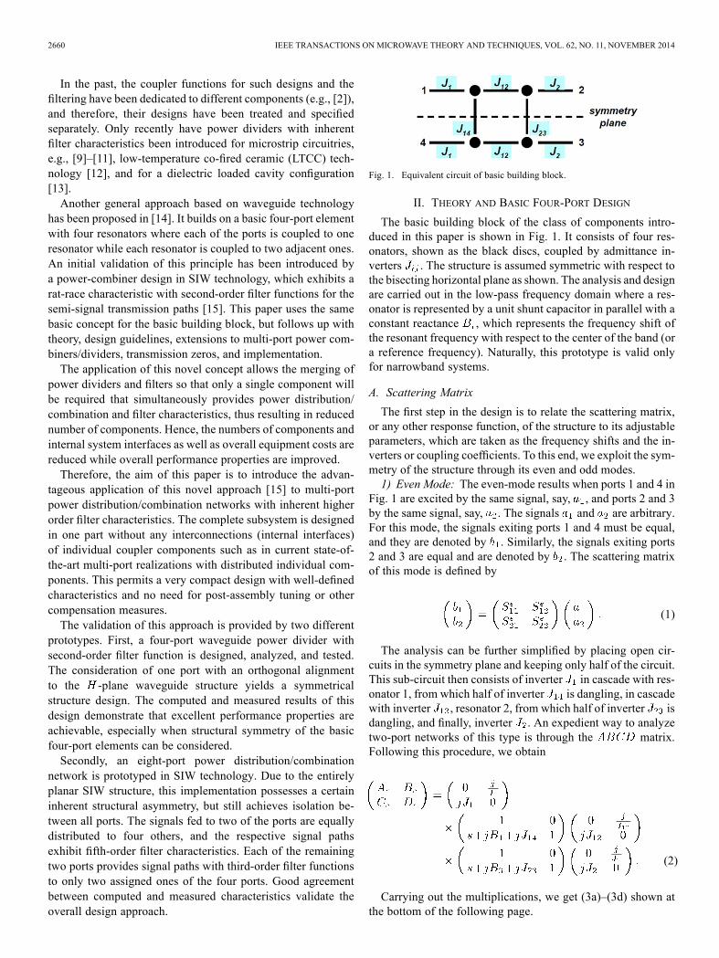
Fig. 1. Equivalent circuit of basic building block.
II. THEORY AND BASIC FOUR-PORT DESIGN
The basic building block of the class of components intro-duced in this paper is shown in Fig. 1. It consists of four res-onators, shown as the black discs, coupled by admittance in-verters . The structure is assumed symmetric with respect tothe bisecting horizontal plane as shown. The analysis and designare carried out in the low-pass frequency domain where a res-onator is represented by a unit shunt capacitor in parallel with aconstant reactance , which represents the frequency shift ofthe resonant frequency with respect to the center of the band (ora reference frequency). Naturally, this prototype is valid onlyfor narrowband systems.
A. Scattering Matrix
The first step in the design is to relate the scattering matrix,or any other response function, of the structure to its adjustableparameters, which are taken as the frequency shifts and the in-verters or coupling coefficients. To this end, we exploit the sym-metry of the structure through its even and odd modes.1) Even Mode: The even-mode results when ports 1 and 4 in
Fig. 1 are excited by the same signal, say, , and ports 2 and 3by the same signal, say, . The signals and are arbitrary.For this mode, the signals exiting ports 1 and 4 must be equal,and they are denoted by . Similarly, the signals exiting ports2 and 3 are equal and are denoted by . The scattering matrixof this mode is defined by
(1)
The analysis can be further simplified by placing open cir-cuits in the symmetry plane and keeping only half of the circuit.This sub-circuit then consists of inverter in cascade with res-onator 1, from which half of inverter is dangling, in cascadewith inverter , resonator 2, from which half of inverter isdangling, and finally, inverter . An expedient way to analyzetwo-port networks of this type is through the matrix.Following this procedure, we obtain
(2)
Carrying out the multiplications, we get (3a)–(3d) shown atthe bottom of the following page.

ROSENBERG et al.: COMPACT MULTI-PORT POWER COMBINATION/DISTRIBUTION WITH INHERENT BANDPASS FILTER CHARACTERISTICS 2661
The scattering matrix of this mode follows from the standardrelations between the matrix and the scattering matrix,normalized to unity in this case, as given in the Appendix.2) Odd Mode: The odd mode can be analyzed similarly to
the even mode. Short circuits are placed in the symmetry plane,keeping only half of the circuit. The matrix of the re-maining half of the circuit is obtained from the matrixof the even mode by changing the signs of and . The re-sult is
(4)
Bymultiplying out these matrices, we get (5a)–(5d), shown atthe bottom of this page. Once the matrices of the evenand odd modes are known, we construct the scattering matricesof each mode and then that of the overall structure according tothe relationship
(6)When the elements of this scattering matrix are calculated,
it is found that their denominator is of order 4 in the complex
frequency with leading term . However, interesting cancel-lations take place when additional constraints are imposed, aswe now discuss.3) Case With , , and : An
examination of the equations relating the parameters toscattering parameters in the Appendix shows that, under theseconditions, the denominators of the scattering matrices of theeven and odd modes are identical. This leads to a reduction inthe order of the denominator of the scattering parameters of theoverall structure from 4 to 2, shown in (7)–(10) at the bottom ofthe following page.The scattering parameters given by (10) show that port 1 is
completely isolated from port 3 and so is port 2 from port 4.This is a direct consequence of the symmetry of the structureand the phase reversal in and . Equation (9) shows thatthe transmission between ports 1 and 4 and that between ports 2and 3 are equal in magnitude, but always 180 out of phase. Thetransmission coefficients between ports 1 and 2 and betweenports 3 and 4 are equal both in magnitude and phase, as shownby (8). Finally, the relative coupling as given by and isdetermined by the ratio .
B. Design for , , and
Since this building block consists of coupled resonators, itcan be designed similarly to coupled-resonator filters. The sym-metry is further exploited to reduce the number of dimensionsthat must be determined. It is, however, worth pointing out thatthe class of second-order responses that can be implemented islimited because of the reduced number of free parameters in thescattering parameters in (7)–(9). We consider a simple exampleto illustrate the procedure.
(3a)
(3b)
(3c)
(3d)
(5a)
(5b)
(5c)
(5d)

2662 IEEE TRANSACTIONS ON MICROWAVE THEORY AND TECHNIQUES, VOL. 62, NO. 11, NOVEMBER 2014
Let us assume that target second-order transmission coeffi-cients of the following forms are sought:
(11)
(12)
The constants and are real with the denomi-nator being a Hurwitz polynomial. The first step is to relate theparameters of the model, , , and to these constants bematching (8) and (11), as well as (9) and (12). The resulting con-straints are
(13a)
(13b)
(13c)
(13d)
For an arbitrary set and there may be no so-lution to (13a)–(13d) with real values of and .This is best illustrated by using an example of a second-order3-dB Chebyshev response.The transmission coefficients are given by
(14)
This expression is obtained from the standard pole-zero de-composition of a second-order Chebyshev filter with a rippleconstant and a return loss of 20 dB.From (13c), we see that . From (13a) and (13b), and
the fact that , we see that .Under this condition, (13c) and (13d) giveand . However, these values do not satisfy (13a)and (13b) since , which is slightly differentfrom . It is also straightforward to confirm thatthe roots of as given by (7) are located at insteadof 0.7071 for a second-order two-pole Chebyshev response.This example confirms that there is no exact solution for a pureChebyshev response for this configuration.Fortunately, very good approximate solutions can be found.
For the same example, an optimized solution leads to
Fig. 2. Responses of the central building block with(solid lines) and the second-order Chebyshev “filter” in
(14) (dashed lines). (a) Wideband response. (b) Expanded view of the passband.
and . A plot of andfor these values along with the transmission coefficient givenby (14) is given in Fig. 2(a). The agreement between the tworesponses is very good over the entire frequency range. In fact,the difference between the two responses is not visible in thisfigure. An expanded view of the passband does show the differ-ence [see Fig. 2(b)].Once the values of the coupling coefficients (inverters) are
known, the design of the central building block follows stan-dard techniques of coupled-resonator filters. Since these are welldocumented, e.g., [16], they are not repeated here.
(7)
(8)
(9)
and
(10)

ROSENBERG et al.: COMPACT MULTI-PORT POWER COMBINATION/DISTRIBUTION WITH INHERENT BANDPASS FILTER CHARACTERISTICS 2663
Fig. 3. Phase characteristics of a basic four-port design (cf. Fig. 1) at 11 GHz(150-MHz bandwidth, return loss 26 dB); red (in online version):
; green (in online version): .
III. DESIGN CONSIDERATIONS FOR MULTIPORT NETWORKS
It is obvious that the general concept introduced in this paperis not only restricted to the designs of four-ports as presented forthe basic building block. The almost arbitrary combination ofbasic four-port elements with additional resonator/filter sectionsallows the design of very compact multi-port subsystems thatcan accommodate a variety of system requirements.In multiport subsystems applications, aspects regarding the
implementation of special filter characteristics and phase re-lations may become important for the individual signal paths.Consequently, the realization of a frequency-selective powerdistribution subsystem has to consider the convenient designand combination of the basic building blocks, possibly withadditional filter sections. Hence, the inherent characteristics ofbasic structures are decisively important.
A. Phase Characteristics
As introduced above, the basic building block exhibits fourports. It provides the splitting of a signal fed to one of the portsinto semi portions occurring at two dedicated other ports, whilethe fourth port is isolated. All ports are matched within the pass-band and the power distribution will not be impaired in prin-ciple by the matching properties terminating the ports. Thus,the principle characteristic within the passband is comparableto that of a magic tee or rat-race ring, e.g., [17]. It dependson whether for the input signal at the feeding port, the powersplitting is in-phase (0 ) or out-of-phase (180 ). Consideringthe basic structure of Fig. 1 with , anin-phase power splitting is achieved for an input signal at port1 and port 4 .Out-of-phase power splitting occurs for signals fed to port 2
and port 3 ,respectively. The analyzed phase characteristics for this basicbuilding block design at 11 GHz with 150-MHz bandwidth areshown in Fig. 3.
Fig. 4. Schematic of eight-port power divider/combiner; gray disks with num-bers indicate ports; basic-block numbering (from left to right) II, I, III.
Consequently, the design of a multiport power distributionnetwork—consisting of the direct combination of several basicbuilding blocks—has to carefully consider the phasing rela-tions of the individual blocks. In other words, for an overalldesign, the configuration of the individually combined blocksis decisively important to satisfy specific phasing requirementsas necessary, for example, for beam-forming networks. How-ever, the relative phasing relation of the individual paths doesnot only depend on the inherent phase relation of the basicblocks. The transmission phase of each path also depends onthe number of resonators and the transformation properties ofthe resonators within individual paths. For example, an extra
mode resonator within a path transforms the phase by180 .
B. Phase Design Example: Eight-Port Power Divider3
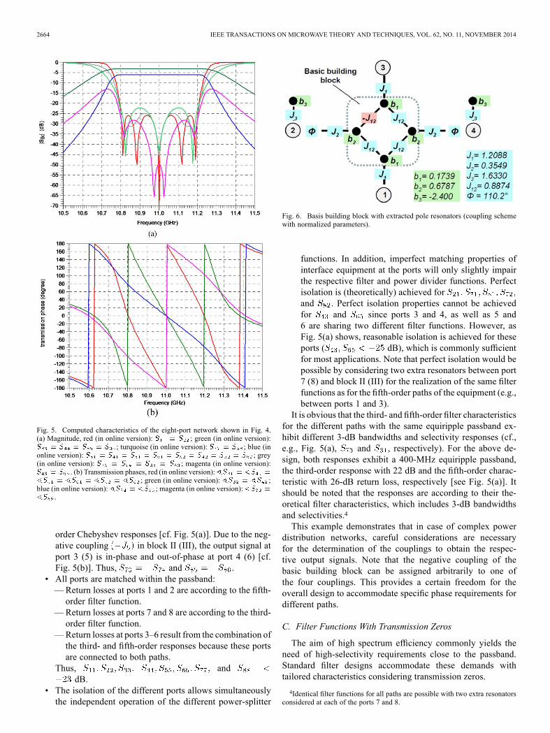
The example of an eight-port frequency-selective power di-vider (cf. schematic in Fig. 4) demonstrates the general designapproach. The subsystem consists of 16 coupled resonators, 12of which are forming three basic building blocks (II, I, III) thatare directly interconnected with couplings . One additionalresonator is attached each to ports 1 and 2. Two other resonatorsare considered at ports 7 and 8.This structure has been optimized to satisfy operation at
11 GHz (bandwidth of 400 MHz) with the following character-istics (cf. coupling values in Fig. 4).• 6-dB power distribution of input signals at port 1 (and 2)to output ports 3–6. These signal paths exhibit five res-onators yielding a fifth-order Chebyshev filter response [cf.Fig. 5(a)]. Considering the paths with the input signal atport 1, all output signals are in-phase. A signal fed to port2 exhibits in-phase signals at ports 5 and 6, while the outputsignals at port 3 and 4 are out-of-phase (due to the nega-tive coupling in block I), as shown in Fig. 4). Thus,
and.
• 3-dB power-splitting functions of input signals at port 7(and 8) to output ports 3 and 4 (5 and 6). The respectivesignal paths have three resonators, thus providing third-
3The description considers the divider case for simplicity—of course the de-sign can be also operated in the reverse direction as a combiner.
2664 IEEE TRANSACTIONS ON MICROWAVE THEORY AND TECHNIQUES, VOL. 62, NO. 11, NOVEMBER 2014
Fig. 5. Computed characteristics of the eight-port network shown in Fig. 4.(a) Magnitude, red (in online version): ; green (in online version):
; turquoise (in online version): ; blue (inonline version): ; grey(in online version): ; magenta (in online version):
. (b) Transmission phases, red (in online version):; green (in online version): ;
blue (in online version): ; magenta (in online version):.
order Chebyshev responses [cf. Fig. 5(a)]. Due to the neg-ative coupling in block II (III), the output signal atport 3 (5) is in-phase and out-of-phase at port 4 (6) [cf.Fig. 5(b)]. Thus, and .
• All ports are matched within the passband:— Return losses at ports 1 and 2 are according to the fifth-order filter function.
— Return losses at ports 7 and 8 are according to the third-order filter function.
— Return losses at ports 3–6 result from the combination ofthe third- and fifth-order responses because these portsare connected to both paths.
Thus, anddB.
• The isolation of the different ports allows simultaneouslythe independent operation of the different power-splitter
Fig. 6. Basis building block with extracted pole resonators (coupling schemewith normalized parameters).
functions. In addition, imperfect matching properties ofinterface equipment at the ports will only slightly impairthe respective filter and power divider functions. Perfectisolation is (theoretically) achieved forand . Perfect isolation properties cannot be achievedfor and since ports 3 and 4, as well as 5 and6 are sharing two different filter functions. However, asFig. 5(a) shows, reasonable isolation is achieved for theseports ( dB), which is commonly sufficientfor most applications. Note that perfect isolation would bepossible by considering two extra resonators between port7 (8) and block II (III) for the realization of the same filterfunctions as for the fifth-order paths of the equipment (e.g.,between ports 1 and 3).
It is obvious that the third- and fifth-order filter characteristicsfor the different paths with the same equiripple passband ex-hibit different 3-dB bandwidths and selectivity responses (cf.,e.g., Fig. 5(a), and , respectively). For the above de-sign, both responses exhibit a 400-MHz equiripple passband,the third-order response with 22 dB and the fifth-order charac-teristic with 26-dB return loss, respectively [see Fig. 5(a)]. Itshould be noted that the responses are according to their the-oretical filter characteristics, which includes 3-dB bandwidthsand selectivities.4
This example demonstrates that in case of complex powerdistribution networks, careful considerations are necessaryfor the determination of the couplings to obtain the respec-tive output signals. Note that the negative coupling of thebasic building block can be assigned arbitrarily to one ofthe four couplings. This provides a certain freedom for theoverall design to accommodate specific phase requirements fordifferent paths.
C. Filter Functions With Transmission Zeros
The aim of high spectrum efficiency commonly yields theneed of high-selectivity requirements close to the passband.Standard filter designs accommodate these demands withtailored characteristics considering transmission zeros.
4Identical filter functions for all paths are possible with two extra resonatorsconsidered at each of the ports 7 and 8.

ROSENBERG et al.: COMPACT MULTI-PORT POWER COMBINATION/DISTRIBUTION WITH INHERENT BANDPASS FILTER CHARACTERISTICS 2665
Fig. 7. Computed responses of configuration in Fig. 6 (with extractedpole); red (in online version): ; green (in online version):
; perfect isolation: .
The basic building block introduced in Section II exhibits asecond-order Chebyshev filter response between all transmis-sion paths. As shown by the example above, the filter order ofa multiport network is increased due to the direct combinationof several blocks, as well as using extra resonators directly cou-pled to the ports of the basic blocks. However, the sequentialcoupling of resonators always yields Chebyshev responses.This general approach, however, is based on coupled res-
onators in the same way as applied for standard filter designs.Thus, extra filter sections that are used for the implementationof transmission zeros (singlets, doublets, etc., as used in mod-ular filter designs [16], [18], [19]) can be employed within thebasic blocks or within the overall multiport network.Two examples are introduced to demonstrate the variety of
possibilities. The schematic of the first example is depicted inFig. 6. In this case, a basic building block is extended symmet-rically at two of its ports with extracted pole resonators. Theparameters (couplings, resonances, and phases between the ex-tracted pole cavities and the assigned resonators of the block)have been determined to satisfy third-order filter characteris-tics at 11 GHz (bandwidth 150 MHz, return loss 25 dB) witha transmission zero at 11.18 GHz (design considerations sim-ilar to [20]). The computed characteristics of this configuration(depicted in Fig. 7) validate this general approach.In the second example, the basic building block is symmetri-
cally associated with two doublets, i.e., each doublet is directlycoupled to a dedicated resonator of the block (cf. schematic inFig. 8). Thus, fourth-order filter responses with one transmis-sion zero are obtained for the transmission paths. The couplingsand resonances are determined to satisfy a filter characteristic at11 GHz (bandwidth 200 MHz, return loss 25 dB) with a trans-mission zero at 11.2 GHz. The computed results of this designin Fig. 9 also verify this design possibility.Thus, it should be noted that the introduced multiport power-
divider approach can be extended by suitable filter sections forthe implementation of advanced filter characteristics with trans-mission zeros. These sections will be directly associated withthe basic building blocks coupled between different blocks or
Fig. 8. Basic building block extended with doublets; coupling scheme withnormalized parameters.
Fig. 9. Computed responses of basic building block with two doublets ac-cording to Fig. 8; red (in online version): ; green (inonline version): ; perfect isolation: .
between blocks and interface ports. They have to be consideredin the overall design since they are improving the filter functionsof the dedicated paths. The examination also includes their ef-fects on the path transmission phases in applications where thephase properties are of special interest. The implementation ofextracted pole solutions is only useful close to interface portssince they require specific phase relations that are commonlyrealized by transmission line sections.
D. General Remarks Regarding Implementation
The above characteristics of the equivalent circuits are basedon the exact values of the dedicated identical parameters (con-sidering also the exact out-of phase conditions of the relatedcouplings, i.e., the symmetry of the structure determined inSection II-B). However, there are commonly special constraintsfor the implementation of physical microwave structures. Oneis related to resonator arrangements allowing the realization ofthe required couplings between dedicated resonators. Anotheraspect applies to the realization of positive and negative cou-plings, especially with identical value, but opposite sign. Theseconstraints entail usually different structures and dimensions,respectively, for the designs of the individual elements. In

2666 IEEE TRANSACTIONS ON MICROWAVE THEORY AND TECHNIQUES, VOL. 62, NO. 11, NOVEMBER 2014
Fig. 10. Photograph of the opened four-port power combination/distributioncomponent in: (a) waveguide technology and (b) port designation.
other words, the design of the structure of each individualelement (resonator, iris) accommodates the realization of thedetermined parameter of the equivalent circuit to satisfy therequired symmetry “electrically.” However, the approximationof the exact values is only achieved in the vicinity of the centerfrequency, which is also known from the equivalent circuitrepresentation in standard filter designs. Especially in caseof different realizations of the same element value, there willbe small differences in the variation of amplitude and phasecharacteristics versus frequency.In the present approach, the effect of these small differences
is especially observed by the impairment of the perfect isolationbetween the assigned ports.Considering for example the design of the basic four-port
structure introduced in Section IV (Figs. 10 and 11). This imple-mentation exhibits single-plane symmetry across ports 1 and 3.The negative coupling is accomplished by a symmetrically cou-pled cavity, yielding identical dimensions of the positiveand negative coupling iris. The intercavity irises coupling res-onator 1 with resonators 2 and 4 are also identical. Due to thissymmetry, the respective transmission signal paths from port1 to port 2 and 4 (as well as from port 3 to 2 and 4) exhibitidentical responses. Thus, almost perfect isolation ( 50 dB) be-tween ports 1 and 3 is observed. (Note that the “non-ideal” value
Fig. 11. Comparisons between theoretical, simulated, and measured scatteringparameters for the four-port prototype in waveguide technology.
of 50 dB of the electromagnetic (EM) simulation can be at-tributed to small imperfections of the modeling.)Compared to this symmetrical port situation of the structure,
a noticeable impairment of the isolation between ports 2 and 4 isobserved (cf. responses of simulation in Fig. 11(b), dB

ROSENBERG et al.: COMPACT MULTI-PORT POWER COMBINATION/DISTRIBUTION WITH INHERENT BANDPASS FILTER CHARACTERISTICS 2667
Fig. 12. Eight-port combiner/divider network in SIW technology with dimensions in millimeters [actual number of via-holes according to the inset in Fig. 15(a)].
within the passband). There is no symmetry for these ports, i.e.,the different paths of the semi-signals through the and
cavities (towards ports 1 and 3, respectively) cause smalldifferences in the transfer characteristics. The comparison of thecomputed amplitude and phase characteristics of the associatedpaths ( and ) within the passband (MHz) exhibits a maximum amplitude imbalance of 0.02 dB
and a maximum phase imbalance of 0.7 . These deviations aremainly the reason for the nonperfect isolation of the assignedports.As this examination demonstrates, implementations with
symmetrical configurations provide the advantage of almostperfect characteristics of the dedicated paths, i.e., no amplitudeand phase imbalance and perfect isolation. However, this isnot a general prerequisite for this approach, i.e., realizationswithout any structural symmetry are feasible. Although suchdesigns will exhibit small deviations of the amplitude andphase characteristics for the individual path responses withinthe passband, they still provide high-performance properties asthe eight-port design example below proves.
IV. RESULTS
This section presents the implementation of the design theoryand considerations for two different multi-port power combina-tion/distribution components.The first circuit is a single-plane symmetric four-port
waveguide circuit that satisfies the conditions outlined inSection II-B. It is designed for a bandwidth of 150 MHz,centered at 11 GHz with a return loss of 26 dB. The normalizedparameters for this design are
and . Fine optimization is performed inthe Wave Wizard. A photograph of the opened prototype isshown in Fig. 10(a). The model of the complete configurationin Wave Wizard including port designation is depicted inFig. 10(b). The component is realized as a structural part thatis completed with a flat lid—made from aluminum using CNCmilling techniques. Note that of port 4 in Fig. 10(b), only theaperture is seen in Fig. 10(a), where this port points into thepage.The basic design consists of an -plane configuration of four
cavities. Each cavity exhibits couplings to one port and the twoadjacent cavities according to the equivalent circuit in Fig. 1.Three of the cavities are utilizing the mode resonanceswhile one cavity (the one associated with port 4) is operatedwith the resonance mode. This allows the utilization ofthe coupling transformation properties (similar as in [21]) ofthis mode to accommodate the prerequisite of inthe planar -plane configuration. The three mode cavi-ties exhibit iris couplings to the dedicated waveguide ports—allof which are realized within the -plane waveguide configu-ration [cf. Fig. 10(a)]. The mode can be also coupledby an -plane iris and waveguide port to maintain an overall-plane configuration (as later considered for the eight-port
SIW application), but this would yield a complete asymmetricstructure—thus in such a case, the principle design demands ofequal coupling values and resonances (cf. Section II-B) are sat-isfied electrically with individual dimensions of the elements,i.e., irises and cavities. However, the optimal “electrical” sym-metry is principally only achieved in the close vicinity of thepassband center frequency, yielding especially a deviation of the

2668 IEEE TRANSACTIONS ON MICROWAVE THEORY AND TECHNIQUES, VOL. 62, NO. 11, NOVEMBER 2014
isolation performance caused by small phase and amplitude im-balances that are increasing from the center frequency towardthe band edges.For the present waveguide implementation, the inherent
asymmetry of an -plane coupled cavity is avoided byconsidering an interface from the top wall (port 4). This is aniris coupling associated with the interface waveguide and islocated in the center of the top wall of the cavity—i.e.,orthogonal to the -plane iris couplings to the adjacent cavities[see Fig. 10(b)]. It is noticed that this implementation exhibitsa single symmetry plane across ports 1 and 3, while the planeacross ports 2 and 4 is still asymmetric, which is finally alsoobserved in the results.Fig. 11 shows comparisons between the simulated and mea-
sured scattering parameters with port numbering depicted inFig. 10(b). It is observed that the measurements agree very wellwith theoretical data obtained from the design procedure inSection II, as well as with simulations—except for the theoret-ically perfect isolation [ in Fig. 11(a) and in Fig. 11(b)]that could be hardly achieved in real implementations. (Notethat the deviations of the selectivity of synthesis and simu-lated/measured results are quite similar to those known fromtypical -plane filter designs.) The measured return loss atall four ports is better than 20 dB, and the 3-dB power com-bination/division capability is demonstrated. The maximuminsertion loss down from the 3-dB level at the center frequencyof 11 GHz is only 0.16 dB for [see Fig. 11(a)] and 0.11 dBfor [see Fig. 11(b)] as well as and [see Fig. 11(c)].The measured isolation between ports 1 and 3 is better than50 dB [see Fig. 11(a)] as a result of the symmetry plane acrossthe respective ports. The measured isolation between oppositeports 2 and 4 is larger than 26 dB, which is still an attractivefigure for power-combiner applications. As mentioned above,this value is attributed to the asymmetry of the configurationacross these ports. Nevertheless, the excellent results in mea-surements and simulations fully verify the design theory.It is obvious that the general concept introduced in this paper
is not only restricted to the designs of four-ports as presentedhere. The almost arbitrary combination of basic four-port ele-ments with additional resonator/filter sections allows the designof very compact multi-port subsystems that can accommodatea variety of system requirements, as for example, those alreadyintroduced by the eight-port example in Section III. In order todemonstrate this point, the eight-port design above was used fora prototype implementation. However, instead of using metalwaveguides, a SIW circuit was used. Fig. 12 shows the circuitlayout and its dimensions.Since a SIW is a planar technology, interfacing of the
-mode cavity in the waveguide version [see Fig. 10(b)]must now be placed in the same plane as all other ports. Thatmakes the circuit completely asymmetric as observed in Fig. 12,and therefore, a larger impact on the isolation properties is ex-pected. Although the symmetric design guidelines presented inSections II and III can still be applied, they must accommodatean “electrical” symmetry considering individual designs ofall elements, i.e., coupling irises and cavities, by an overallfine optimization. To accommodate the planar structure, the
-mode cavity of the basic design above is now coupled
Fig. 13. Comparisons between simulated and measured scattering parametersfor the eight-port prototype in SIW technology. (a) to . (b) to
.
at the sidewall opposite to the iris couplings with the adjacentcavities of the basic four resonator block. An additionalcavity is considered between this coupling and the respectiveinterface at all these ports—as can be seen in Fig. 12 at ports2, 7, and 8. Another extra resonator is also considered at port1. It should be noted that these extra resonators do not prin-cipally have an influence on the coupling function, but theyare increasing the filter functions of the dedicated paths (cf.Section III). The implementation depicted in Fig. 12 with align-ment of the basic blocks to each other and the extra resonatorscorresponds to the equivalent circuit design in Fig. 4. Thus, thepaths from port 1 (2) to 3–6 exhibit a fifth-order filter responsewith 6-dB power distribution while the paths from port 7 (8)to 3, 4 (5, 6) have a third-order filter characteristic with 3-dBpower distribution.Following the synthesis procedure, an all-dielectric wave-
guide component using commercial software such as WaveWizard is designed for a bandwidth of 400 MHz at center fre-quency of 11 GHz. The structure is then transferred to SIW tech-nology according to equivalent waveguide widths reported in

ROSENBERG et al.: COMPACT MULTI-PORT POWER COMBINATION/DISTRIBUTION WITH INHERENT BANDPASS FILTER CHARACTERISTICS 2669
Fig. 14. Comparisons between simulated and measured scattering parametersfor the eight-port prototype in SIW technology; to .
[22]. However, fine optimization of all resonator and couplingparameters within HFSS is required to adjust for the transfer toSIW technology. In order to ease the many different require-ments of this circuit, the optimization applied in this case fa-vored amplitude over phase response.The eight-port power divider/combiner is designed for an
RT/Duroid 6002 substrate with , loss tangent 0.0012,substrate thickness mm, conductor thickness
m, and conductivity S/m. The diameter ofall via-holes is 1 mm with center-to-center spacing of 1.4 mm atall ports. For access with measurement equipment, all ports areinterfaced with SIW-to-microstrip transitions according to [23].In order to limit the number of figures, we present a selec-
tion of scattering parameters of the eight-port combiner/divider.Fig. 13 presents a comparison between simulation and mea-surements for parameters with . Reasonableagreement between simulations and measurements is obtaineddespite the fact that the original assumption of symmetry is vi-olated. Measured return loss values in the order of 20 dB aredemonstrated [see Fig. 13(a)], and the input power at port oneis divided between ports 3–6 while ports 2, 7, and 8 are isolatedto at least 20 dB.Several discrepancies between measurements and simu-
lations are observed. First of all, there is an added insertionloss of up to 3 dB compared to the simulations that includeconductor and dielectric losses. This is comparable with manypublished SIW filters whose insertion losses are in the order of2 dB, e.g., [24]. Secondly, the measured return loss is worsethan simulated and the isolation peak in and [seeFig. 13(b)] is not reproduced. And thirdly, a slight frequencyshift towards higher frequencies is observed.The frequency shift can in part be attributed to the toler-
ance of the dielectric constant, but mostly to the fact that aslightly larger drill size was used in the manufacturing process.That makes the via-holes larger and the resonators effectivelysmaller, thus shifting the frequency upwards. This may also bea reason for the degraded return loss as couplings are changed.The other deviations are mainly due to the measurement set
Fig. 15. (a) Photograph of the eight-port SIW prototype and comparisons be-tween simulated and measured phase differences for ports with in-phase andout-of-phase power combination/division and (b) comparison between simu-lated and measured transmission phases.
up. Due to the size of the circuit (Fig. 12), a test fixture couldnot be used so that all measurements had to be performed withcoaxial connectors attached to all ports and to all calibrationstandards. (TRL calibration standards were used to deembed thecoax-to-microstrip-to-SIW transitions.) The different solderingof all such connectors influences the calibration, and thus themeasurements. Moreover, only two ports can be deembedded atthe same time while the remaining six ports are terminated withcoaxial terminations. Thus, the reflections and losses causedby microstrip transitions and coaxial connectors fully influencethe measurements, resulting in added reflections and estimatedadded losses of up to 1 dB within the circuit.Fig. 14 shows the scattering parameters related to one of the
side ports, port 8. A signal fed into port 8 is divided betweenports 5 and 6, while all other ports such as port 4 [or port 1from Fig. 13(b)] are isolated. Due to the lower filter order (threeinstead of five), the added loss is less than 1.5 dB compared tothose parameters displayed in Fig. 13 (e.g., 3.8 dB simulatedand 5.2 dB measured). The measurement of also showsthe limitations in the dynamic range.

2670 IEEE TRANSACTIONS ON MICROWAVE THEORY AND TECHNIQUES, VOL. 62, NO. 11, NOVEMBER 2014
The inset of Fig. 15(a) shows the SIW prototype. In order toexplore the phase relationships within the passband, Fig. 15(a)displays comparisons between simulated and measured phasedifferences for in-phase and out-of-phase combining ports. Port1 is divided in-phase between ports 3 and 5 (and ports 4 and6). The agreement between measurements and simulations isreasonable with a maximum deviation of about 20°. A signal fedinto port 8 is divided to ports 5 and 6. This division is out-of-phase due to the mode in one of the cavities attached toport 8. The agreement between measurements and simulationsis very good, albeit the fact that the difference is 200° instead of180°.In order to investigate these discrepancies, Fig. 15(b) displays
the four transmission phases when feeding port 1 in the vicinityof the center frequency. It is observed that the simulated phasesof and as well as those of and agree, but thatthere is about a 25° difference between the two. This is a re-sult of having optimization focus mainly on amplitude response.However, the phase measurements of and (to the leftof the input port) are off by about 10° and 20°, respectively,whereas those of and are in good agreement. This pointsto tolerances in the fabrication of the prototype on top of the sol-dering of connectors to the calibration standards. However, theoverall performance is also a result of optimizing a completelyasymmetric structure that cannot make use of all of the sym-metry conditions assumed in Sections II and III. An all-metalwaveguide version of this eight-port combiner/divider with thesymmetrically coupled cavity would have ports 2, 7, and8 (Fig. 12) pointing upwards [cf. port 4 in Fig. 10(b)], thusyielding improved performance properties due to the utiliza-tion of the one-plane structure symmetry of the basic buildingblocks.
V. CONCLUSION
The compact and frequency-selective multi-port powercombiner/divider networks introduced in this paper presentattractive solutions for modern communication systems. Theapproach is based on a basic four-port building block consistingof four directly coupled resonators. Multiport networks arerealized by the direct coupling of several such building blocks.Moreover, additional cavities or complete filter sections (e.g.,doublets, triplets, etc.) can be directly coupled between thebuilding blocks or at their interfaces to accommodate specialfilter characteristics/requirements between individual ports.Consequently, this general concept offers a high degree offreedom in the design of multiport power divider/combiner net-works with isolated/decoupled ports—providing additionallyalmost arbitrary filter functions between the ports. The designapproach is entirely based on filter theory since all cavities ofthe structure are directly coupled. Thus, the solution does notonly provide the merging of filter and combiner functions, italso facilitates very compact implementations, which is anotherimportant advantage. The measurements on the symmetricall-metal waveguide four-port prototype verify the designtheory by excellent agreement with simulations. An eight-portprototype demonstrates the possible extension of the four-portelement and the use of SIW technology. Due to limitationsin port orientation in planar circuits, the unavoidable total
asymmetry encountered in SIW yields a reduced performancecompared with the all-metal waveguide circuit. However, theoperational principle applies in approximation and provides areasonable alternative when very compact planar circuitry isenvisaged.
APPENDIX
The scattering parameters of the even/odd modes are given interms of the respective normalized parameters as
(A.1)
By using the expressions of the elements of the matrixof the even mode as given by (3a)–(3d), the denominator of thescattering parameters of this mode becomes
(A.2)
Similarly, the denominator of the scattering parameters of theodd mode becomes
(A.3)
If we now assume that and ,(A.2) gives
(A.4)

ROSENBERG et al.: COMPACT MULTI-PORT POWER COMBINATION/DISTRIBUTION WITH INHERENT BANDPASS FILTER CHARACTERISTICS 2671
Under the same conditions, (A.3) becomes
(A.5)
Under these conditions, (A.4) and (A.5) show thatand . Since the denominators of the scat-
tering parameters of the even and odd modes are identical, theoverall scattering parameters have the same denominator as in(6). Each parameter has a denominator of second order. In thegeneral case, each denominator of the scattering parameters ofthe central block is of order 4.
ACKNOWLEDGMENT
The authors would like to thank Prof. J. Hesselbarth, Univer-sity of Stuttgart, Stuttgart, Germany, for taking care of the pre-cise manufacturing of the four-port power combiner, and Prof.M. Schneider and H. Masemann, both with the University ofBremen, Bermen, Germany, for accurate measurement of thewaveguide component.
REFERENCES
[1] R. N. Simons, E. G. Wintucky, J. D. Wilson, and D. A. Force,“Ultra-high power and efficiency space traveling-wave tube amplifierpower combiner with reduced size and mass for NASA missions,”IEEE Trans. Microw. Theory Techn., vol. 57, no. 3, pp. 582–588, Mar.2009.
[2] F. F. He, K. Wu,W. Hong, L. Han, and X.-P. Chen, “Low-cost 60-GHzsmart antenna receiver subsystem based on substrate integrated wave-guide technology,” IEEE Trans. Microw. Theory Techn., vol. 60, no. 4,pp. 1156–1165, Apr. 2012.
[3] J. Uher, J. Bornemann, and U. Rosenberg, Waveguide Components forAntenna Feed Systems: Theory and CAD. Boston, MA, USA: ArtechHouse, 1993.
[4] H. J. Riblet, “The short-slot hybrid,” Proc. IRE, vol. 40, no. 2, pp.180–184, Feb. 1952.
[5] U. Rosenberg and K. Beis, “Improved narrow-wall short slot couplerdesign exhibiting significant increased bandwidth and low cost produc-tion,” in Proc. 31st Eur. Microw. Conf., London, U.K., Sep. 2001, pp.1–4.
[6] K. Song, X. Ren, F. Chen, and Y. Fan, “Compact in-phase power di-vider integrated filtering response using spiral resonator,” IET Microw.Antennas Propag., vol. 8, no. 4, pp. 228–234, 2014.
[7] K. Song, F. Chen, F. Zhang, and Y. Fan, “Synthesis and design methodof bandpass-response power divider,”Microelectron. J., vol. 45, no. 1,pp. 71–77, Jan. 2014.
[8] R. Gomez-Garcıa, M. Sanchez-Renedo, and J.-M. Munoz-Ferreras,“Microwave filtering power-distribution networks,” in IEEE MTT-SInt. Microw. Symp. Dig., Baltimore, MD, USA, Jun. 2011, pp. 1–4.
[9] F. Lin, Q.-X. Chu, and S. W. Wong, “Design of dual-band filteringquadrature coupler using and resonators,” IEEE Microw.Wireless Compon. Lett., vol. 22, no. 11, pp. 565–567, Nov. 2012.
[10] C.-H. Wu and C. H. Chen, “Compact LTCC bandpass 180 hybridusing lumped single-to-differential and single-to-common bandpassfilters,” in IEEE MTT-S Int. Microw. Symp. Dig., Boston, MA, USA,Jun. 2009, pp. 1473–1476.
[11] W.-M. Chau, K.-W. Hsu, and W.-H. Tu, “Filter-based Wilkinsonpower divider,” IEEE Microw. Wireless Compon. Lett., vol. 24, no. 4,pp. 239–241, Apr. 2014.
[12] H. Uchida, N. Yoneda, Y. Konishi, and S. Makino, “Bandpass direc-tional couplers with electromagnetically-coupled resonators,” in IEEEMTT-S Int. Microw. Symp. Dig., San Francisco, CA, USA, May 2006,pp. 1563–1566.
[13] Y. J. Cheng and Y. Fan, “Compact substrate-integrated waveguidebandpass rat-race coupler and its microwave applications,” IET Mi-crow. Antennas Propag., vol. 6, no. 9, pp. 1000–1006, Sep. 2012.
[14] U. Rosenberg and S. Amari, “New power distribution (combination)method with frequency selective properties,” in Eur. Microw. Conf.,Amsterdam, The Netherlands, Oct./Nov. 2012, Workshop Notes W14:advances of -port networks for space application.
[15] U. Rosenberg, M. Salehi, J. Bornemann, and E. Mehrshahi, “A novelfrequency-selective power combiner/divider in single-layer substrateintegrated waveguide technology,” IEEE Microw. Wireless Compon.Lett., vol. 23, no. 8, pp. 406–408, Aug. 2013.
[16] R. J. Cameron, C.M.Kudsia, and R. R.Mansour, Microwave Filters forCommunication Systems: Fundamentals, Design and Applications.New York, NY, USA: Wiley, 2007.
[17] D. M. Pozar, Microwave Engineering, 3rd ed. New York, NY, USA:Wiley, 2005.
[18] S. Amari and U. Rosenberg, “New building blocks for modular de-sign of elliptic and self-equalized filters,” IEEE Trans. Microw. TheoryTechn., vol. 52, no. 2, pp. 721–736, Feb. 2004.
[19] S. Amari and U. Rosenberg, “The doublet: A new building block formodular design of elliptic filters,” in Proc. 32nd Eur. Microw. Conf.,Milan, Italy, Oct. 2002, pp. 1–3.
[20] S. Amari and U. Rosenberg, “Synthesis and design of novel in-linefilters with one or two real transmission zeros,” IEEE Trans. Microw.Theory Techn., vol. 52, no. 5, pp. 1464–1478, May 2004.
[21] U. Rosenberg, “New ‘planar’ waveguide cavity elliptic function fil-ters,” in Proc. 25th Eur. Microw. Conf., Bologna, Italy, Sep. 1995, pp.524–527.
[22] M. Salehi and E. Mehrshahi, “A closed-form formula for dispersioncharacteristics of fundamental SIW mode,” IEEE Microw. WirelessCompon. Lett., vol. 21, no. 1, pp. 4–6, Jan. 2011.
[23] D. Deslandes, “Design equations for taperedmicrostrip-to-substrate in-tegrated waveguide transitions,” in IEEE MTT-S Int. Microw. Symp.Dig., Anaheim, CA, USA, May 2010, pp. 704–704.
[24] M. Salehi, J. Bornemann, and E. Mehrshahi, “Compact folded sub-strate integrated waveguide filter with non-resonating nodes for high-selectivity bandpass applications,” in Proc. 43rd Eur. Microw. Conf.,Nuremberg, Germany, Oct. 2013, pp. 155–158.
Uwe Rosenberg (M’89–SM’93) received theDipl. Ing. degree (first-class honors) in electricalengineering (telecommunication technique) fromthe Fachhochschule der Deutschen Bundespost,Dieburg, Germany, in 1982.From 1982 to 1983, he was with Hydro Therm,
Dieburg, Germany, where he was involved with thedesign and development of automatic safety andheating control circuits. From 1983 to 1985, he waswith the Technische Hochschule Darmstadt, Darm-stadt, Germany, where he was involved with the
design and development of experimental installations and software componentsfor microcomputer control systems. In 1985, he joined the Space Division,ANT Nachrichtentechnik GmbH (now Tesat-Spacecom GmbH & Co. KG),Backnang, Germany, where he was engaged in research and development ofmicrowave filters, multiplexers, and passive subsystems for communicationssatellites. From 1989 to 2008 he was Head of the Research and DevelopmentLaboratory for Passive Microwave Components and Subsystems, EricssonGmbH (which was, until December 2005, Marconi Communications GmbH,and formerly Bosch Telecom GmbH, Public Networks Division), Backnang,Germany. During this period, he was in charge of research and development ofintegrated waveguide transceiver circuitry’s, channel branching networks (mul-tiplexers), antenna feed and waveguide (feeder) systems for trunk and accessradio applications, mobile base stations, large earth stations, and defense andcommunications satellites. From 2006 to 2008, he was additionally appointedto Manager of the Antenna Development Team. In 2002, he started his ownproject and consultancy work for international companies with the design ofnovel passive microwave designs and subsystems for a variety of applications(earth stations, satellites, millimeter-wave communications equipment, mobile,defense, etc.) providing design, measurement, production, and technologysupport and advice. Since 2011, he has been the Managing Director withMician Global Engineering GbR, Bremen, Germany, which he cofoundedthe same year together with partners. He coauthored Waveguide Componentsfor Antenna Feed Systems: Theory and CAD (Artech House, 1993). He hasauthored or coauthored over 100 technical papers and has originated more than50 granted microwave design patents.Mr. Rosenberg is a member of Verband der Elektrotechnik Elektronik Infor-
mationstechnik (VDE), Informationstechnische Gesellschaft (ITG), and Verein

2672 IEEE TRANSACTIONS ON MICROWAVE THEORY AND TECHNIQUES, VOL. 62, NO. 11, NOVEMBER 2014
Deutscher Ingenieure (VDI). He is also a member of the European MicrowaveAssociation (EuMA). He is a senior member of the IEEE Microwave Theoryand Techniques Society (IEEE MTT-S) and the IEEE Antennas and Propaga-tion Society (IEEE AP-S).
Mehdi Salehi was born in Isfahan, Iran, in 1979. Hereceived the B.Sc. and M.Sc. degrees in electrical en-gineering from the Isfahan University of Technology(IUT), Isfahan, Iran, in 2001 and 2006, respectively,and the Ph.D. degree in electrical engineering fromShahid Beheshti University (SBU), Tehran, Iran, in2013.From 2011 to 2013, he was a Research Assistant
with the CADMIC Group, University of Victoria,Victoria, BC, Canada, where he was involved withdesign, analysis, and synthesis of substrate inte-
grated waveguide (SIW) structures. He is currently a Postdoctoral Fellow withthe Coding Signal Transmission (CST) Laboratory, University of Waterloo,Waterloo, ON, Canada, where he is engaged in simulation and hardwareimplementation of wireless communication systems. His research interestsinclude computer-aided design of RF and microwave structures, numericalmethods in electromagnetics, and advanced microwave and millimeter-wavecircuits and components.
Smain Amari received the D.E.S. degree in physicsand electronics from Constantine University, Con-stantine, Algeria, in 1985, and the Masters degree inelectrical engineering and Ph.D. degree in physicsfrom Washington University, St. Louis, MO, USA,in 1989 and 1994, respectively.From 1994 to 2000, he was with the Department of
Electrical and Computer Engineering, University ofVictoria, Victoria, BC, Canada. From 1997 to 1999,he was a Visiting Scientist with the Swiss Federal In-stitute of Technology, Zurich, Switzerland, and a Vis-
iting Professor in Summer 2001. In 2006, he was a Visiting Professor with theUniversity of Ulm, Ulm, Germany. Since November 2000, he has been withthe Department of Electrical and Computer Engineering, Royal Military Col-
lege of Canada, Kingston, ON, Canada, where he is currently a Professor. He isinterested in numerical analysis, numerical techniques in electromagnetics, ap-plied physics, applied mathematics, wireless and optical communications, com-puter-aided design (CAD) of microwave components, and the application ofquantum field theory in quantum many-particle systems.
Jens Bornemann (M’87–SM’90–F’02) receivedthe Dipl.-Ing. and Dr.-Ing. degrees in electrical en-gineering from the University of Bremen, Bremen,Germany, in 1980 and 1984, respectively.From 1984 to 1985, he was a Consulting Engineer.
In 1985, he joined the University of Bremen, as anAssistant Professor. Since April 1988, he has beenwith the Department of Electrical and ComputerEngineering, University of Victoria, Victoria, BC,Canada, where he became a Professor in 1992.From 1992 to 1995, he was a Fellow of the British
Columbia Advanced Systems Institute. In 1996, he was a Visiting Scientistwith Spar Aerospace Limited (now MDA Space), Ste-Anne-de-Bellevue, QC,Canada, and a Visiting Professor with the Microwave Department, Universityof Ulm, Ulm, Germany. From 1997 to 2002, he was a Co-Director of the Centerfor Advanced Materials and Related Technology (CAMTEC), Universityof Victoria. In 2003, he was a Visiting Professor with the Laboratory forElectromagnetic Fields and Microwave Electronics, ETH Zurich, Switzerland.He coauthored Waveguide Components for Antenna Feed Systems—Theoryand Design (Artech House, 1993). He has authored or coauthored over 300technical papers. His research activities include RF/wireless/microwave/mil-limeter-wave components and systems design and field-theory-based modelingof integrated circuits, feed networks, and antennas.Dr. Bornemann is a Registered Professional Engineer in the Province of
British Columbia, Canada. He is a Fellow of the Canadian Academy of Engi-neering (CAE). He serves on the Editorial Advisory Board of the InternationalJournal of Numerical Modelling. From 1999 to 2002, he was an associate editorfor the IEEE TRANSACTIONS ON MICROWAVE THEORY AND TECHNIQUES in thearea of microwave modeling and computer-aided design (CAD). From 2006 to2008, he was an associate editor for the International Journal of Electronicsand Communications. From 1999 to 2009, he served on the Technical ProgramCommittee of the IEEE Microwave Theory and Techniques Society (IEEEMTT-S) International Microwave Symposium.