ieee transactions on electron devices, vol. …bora/journals/2008/ted08.pdf · 72 ieee transactions...
TRANSCRIPT

IEEE TRANSACTIONS ON ELECTRON DEVICES, VOL. 55, NO. 1, JANUARY 2008 71
Design in the Power-Limited Scaling RegimeBorivoje Nikolic, Senior Member, IEEE
(Invited Paper)
Abstract—Technology scaling has entered a new era, wherechip performance is constrained by power dissipation. Powerlimits vary with the application domain; however, they dictate thechoices of technology and architecture and necessitate implemen-tation techniques that tradeoff performance for power savings.This paper examines technology options in the power-limited-scaling regime and reviews sensitivity-based analysis that can beused for the optimal selection of optimal architectures and circuitimplementations to achieve the best performance under powerconstraints. These tradeoffs are examined in the context of powerminimization at the technology, circuit, logic, and architecturelevels, both at the design and run times.
Index Terms—CMOS, performance, power, technology scaling.
I. INTRODUCTION
T ECHNOLOGY scaling reduces the minimum physicaldimensions of transistors by a factor of S = 0.7 in each
generation, and interconnect scaling follows a similar trend.Accordingly, the area needed to implement digital logic func-tions and memory has been reducing roughly by half with theintroduction of each new technology node. In addition, scaleddevices have simultaneously been increasing switching speedand lowering switching energy. The ideal scaling scenarioproposed by Dennard et al. [1] requires that all voltages scaleby the same factor of 0.7 in order to maintain constant fields.Consequently, switching energy per transistor has been scalingdown by a factor of S3, resulting in constant power for a chipwith the same area. A limitation of this scaling regime, aspointed out in the original paper, is that kT/q does not scale,resulting in nonscaling of device subthreshold characteristics.Ideal scaling does not account for gate tunneling currents,which are significant with very thin gate oxides.
Practical scaling has not always followed this ideal principle.Supply voltages were maintained at high levels of 12 V, and foran extended period of time at 5 V, to maintain compatibilityof chip-to-chip interfaces. Supply-voltage scaling started atapproximately the 0.5-µm technology node and, until veryrecently, has roughly followed the scaling of linear dimensions.
Manuscript received September 20, 2007. This work was supported in part byThe National Science Foundation Infrastructure Grant 0403427, by the Centerfor Circuit & System Solutions (C2S2) Focus Center, by a Semiconductor Re-search Corporation program, and by an NSF CAREER Grant ECCS 0238572.The review of this paper was arranged by Editor T.-J. K. Liu.
The author is with the Department of Electrical Engineering and ComputerSciences, University of California at Berkeley, Berkeley, CA 94720-1770 USA(e-mail: [email protected]).
Color versions of one or more of the figures in this paper are available onlineat http://ieeexplore.ieee.org.
Digital Object Identifier 10.1109/TED.2007.911350
Fig. 1. (a) Frequency and (b) power trends in Intel’s microprocessors.
However, designers and manufacturers have often used some-what higher supply voltages above the ideal values of VDD =feature size × 10 V/µm to boost the performance within reli-ability constraints. In addition, chip dimensions have tradition-ally been increasing rather than staying constant. Specificallyin microprocessor design, architectural changes have resultedin increased operating frequencies, beyond the gains achievableby technology scaling alone [2], [3]. Fig. 1(a), as an example,shows the frequency trends in Intel’s lead microprocessors overtime. All these factors have resulted in a rapid increase in powerdissipation. Fig. 1(b) shows the increase in power dissipation inIntel’s processors, and the data from other manufacturers followa similar trend. Over the last 10 years, the power dissipationin the lead microprocessors has increased by a factor of 2.5per generation, saturating at about 100-W levels. In high-performance (HP) applications, power dissipation is limited
0018-9383/$25.00 © 2008 IEEE

72 IEEE TRANSACTIONS ON ELECTRON DEVICES, VOL. 55, NO. 1, JANUARY 2008
by the practicality and the cost of cooling; in the case ofmicroprocessors with forced-air cooling systems, this limit is inthe 100–150-W range. Chips for portable applications often donot allow the use of fans and are limited to about 2 W of powerwith plastic packaging. Mobile applications are often limitedby the battery life, which dictates constraints on both active andleakage powers during the standby and sleep modes. As a result,most of the designs today and all of the designs in the future arepower-limited.
These trends in technology scaling have made power dissipa-tion a primary design constraint for both HP and mobile appli-cations. In contrast to the past, fitting within the power budgettoday is as important for the designers as is achieving maxi-mum performance; instead of targeting the absolute maximumperformance, the designers need to maximize the performancefor the given power budget. There are many degrees of freedomfor trading off performance and power in the design: They canbe traded off at the technology selection stage, in circuit andlogic design, and at the architecture optimization stage. Manyof the decisions in system design are dependent on each otherand can involve optimization of both discrete and continuousvariables.Device and Circuit Models: The energy and the delay of a
logic gate are functions of its size, supply voltage, and transistorthreshold voltage. It is important to model the current in thesaturation and subthreshold regions to evaluate the performanceof scaled circuits. NMOS current in the saturation region canbe accurately modeled as a function of the gate–source anddrain–source voltages [4], [5]
IDSat =W
L
µeffCoxECL
2(VGS − VTh)2
(VGS − VTh) + ECL(1 + λVDS)
(1)
where µeff is the electron/hole mobility, Cox is the gate capac-itance per unit area, W and L are the width and the length ofthe channel, respectively, VTh is the threshold voltage, EC is afit for the saturation field, and the parameter λ can be fitted toinclude the effect of drain-induced barrier lowering (DIBL), aswell as of channel-length modulation.
Power dissipation in digital circuits, in general, has fourcomponents: active, leakage, short circuit, and biasing
P = Psw + Pleak + Psc + Pbias. (2)
Power dissipation is dominated by the switching and leakagecomponents. The short-current power is proportional to theswitching power for well-designed circuits [6], and for thepurpose of scaling, analysis can be treated together. Biasingcurrents often exist for generating reference voltages and cur-rents in memory and I/O circuits, and some less-often-usedlogic families. Switching power is equal to the rate of energyexchange and is therefore a product of switching energy andthe frequency of operation
Psw = Eswf = αCV 2DDf (3)
where Esw is the switching energy, C is the total capacitanceunder consideration (can be a gate, logic path, or an entire chip),α is the switching activity, and f is the operating frequency.
The subthreshold current is a function of gate-to-source anddrain-to-source voltages
Isubth = µeffCoxW
LV 2
t
× exp(
VGS − VTh
nVt
)(1 − exp
(−VDS
Vt
))(4)
where Vt = kT/q is the thermal voltage, and n is the sub-threshold parameter [5]. The subthreshold slope Ssubth is oftendefined as Ssubth = ln 10nVt.
Leakage power is the product of the supply voltage andleakage current Ileak
Pleak = VDDIleak (5)
where Ileak corresponds to the subthreshold current (Isubth),with VGS = 0
Ids,leak = µeffCoxW
L(n − 1)V 2
t e−VTh/Vt . (6)
In present technologies that use SiO2 as the gate dielectric(90, 65, and some of 45 nm), there is a significant contributionof the gate leakage current, which has been increasing withthinning of the gate oxides. This trend will be temporarilydiscontinued with the introduction of high-k dielectrics in the45-nm node [7], [8]. As a result, in the remainder of this paper,less attention will be paid in treating gate leakage currents.Constant-Field Scaling: In the conventional scaling model,
the device dimensions (W , L, and tox) scale by the factor of S.The doping concentration increases by the factor 1/S in orderto scale down the junction depths, and voltages VDD and VTh
scale down linearly with S.The constant-field-scaling regime keeps the chip active
power density constant by scaling the active power per devicewith a factor of S2. This model results in constant powerdissipation for a fixed area in a scaled technology if the leakagepower is negligible. In the early period of technology scaling,the leakage component of the overall power dissipation hasbeen, indeed, small; however, scaling of the threshold voltagehas been increasing the leakage exponentially.
Under the constant-field scaling by a factor of S, the leakagepower for the chip with a constant area can be shown using (6)to scale with a factor of (1/S2)10(VTh(1−S)/Ssubth). The relativeincrease in leakage current is dependent on the actual value ofthe threshold voltage. Threshold reduction by a factor of S =0.7 increases the chip leakage power density by several ordersof magnitude, with high values of threshold voltages (> 0.5 V).However, this traditionally did not affect the overall powerconsumption as the subthreshold leakage was a very smallcomponent of the total power, even smaller than reverse biasjunction leakage currents. A continued exponential increase inleakage currents has brought them to a level where they signif-icantly contribute to the overall power budget. In sub-100-nmprocesses, this increase in leakage is less than an order ofmagnitude with each technology generation (about 2–3×) sinceSVTh < Ssubth.
NIKOLIC: DESIGN IN THE POWER-LIMITED SCALING REGIME 73
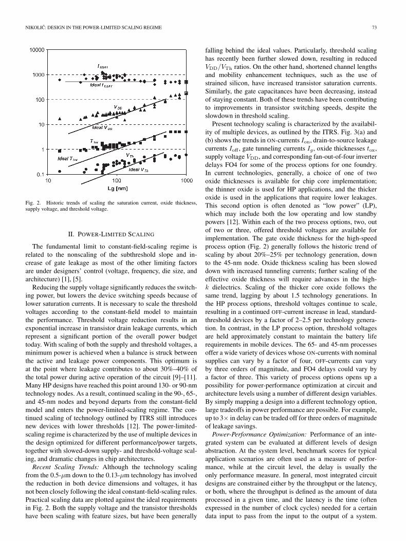
Fig. 2. Historic trends of scaling the saturation current, oxide thickness,supply voltage, and threshold voltage.
II. POWER-LIMITED SCALING
The fundamental limit to constant-field-scaling regime isrelated to the nonscaling of the subthreshold slope and in-crease of gate leakage as most of the other limiting factorsare under designers’ control (voltage, frequency, die size, andarchitecture) [1], [5].
Reducing the supply voltage significantly reduces the switch-ing power, but lowers the device switching speeds because oflower saturation currents. It is necessary to scale the thresholdvoltages according to the constant-field model to maintainthe performance. Threshold voltage reduction results in anexponential increase in transistor drain leakage currents, whichrepresent a significant portion of the overall power budgettoday. With scaling of both the supply and threshold voltages, aminimum power is achieved when a balance is struck betweenthe active and leakage power components. This optimum isat the point where leakage contributes to about 30%–40% ofthe total power during active operation of the circuit [9]–[11].Many HP designs have reached this point around 130- or 90-nmtechnology nodes. As a result, continued scaling in the 90-, 65-,and 45-nm nodes and beyond departs from the constant-fieldmodel and enters the power-limited-scaling regime. The con-tinued scaling of technology outlined by ITRS still introducesnew devices with lower thresholds [12]. The power-limited-scaling regime is characterized by the use of multiple devices inthe design optimized for different performance/power targets,together with slowed-down supply- and threshold-voltage scal-ing, and dramatic changes in chip architectures.Recent Scaling Trends: Although the technology scaling
from the 0.5-µm down to the 0.13-µm technology has involvedthe reduction in both device dimensions and voltages, it hasnot been closely following the ideal constant-field-scaling rules.Practical scaling data are plotted against the ideal requirementsin Fig. 2. Both the supply voltage and the transistor thresholdshave been scaling with feature sizes, but have been generally
falling behind the ideal values. Particularly, threshold scalinghas recently been further slowed down, resulting in reducedVDD/VTh ratios. On the other hand, shortened channel lengthsand mobility enhancement techniques, such as the use ofstrained silicon, have increased transistor saturation currents.Similarly, the gate capacitances have been decreasing, insteadof staying constant. Both of these trends have been contributingto improvements in transistor switching speeds, despite theslowdown in threshold scaling.
Present technology scaling is characterized by the availabil-ity of multiple devices, as outlined by the ITRS. Fig. 3(a) and(b) shows the trends in ON-currents Ion, drain-to-source leakagecurrents Ioff , gate tunneling currents Ig , oxide thicknesses tox,supply voltage VDD, and corresponding fan-out-of-four inverterdelays FO4 for some of the process options for one foundry.In current technologies, generally, a choice of one of twooxide thicknesses is available for chip core implementation;the thinner oxide is used for HP applications, and the thickeroxide is used in the applications that require lower leakages.This second option is often denoted as “low power” (LP),which may include both the low operating and low standbypowers [12]. Within each of the two process options, two, outof two or three, offered threshold voltages are available forimplementation. The gate oxide thickness for the high-speedprocess option (Fig. 2) generally follows the historic trend ofscaling by about 20%–25% per technology generation, downto the 45-nm node. Oxide thickness scaling has been sloweddown with increased tunneling currents; further scaling of theeffective oxide thickness will require advances in the high-k dielectrics. Scaling of the thicker core oxide follows thesame trend, lagging by about 1.5 technology generations. Inthe HP process options, threshold voltages continue to scale,resulting in a continued OFF-current increase in lead, standard-threshold devices by a factor of 2–2.5 per technology genera-tion. In contrast, in the LP process option, threshold voltagesare held approximately constant to maintain the battery liferequirements in mobile devices. The 65- and 45-nm processesoffer a wide variety of devices whose ON-currents with nominalsupplies can vary by a factor of four, OFF-currents can varyby three orders of magnitude, and FO4 delays could vary bya factor of three. This variety of process options opens up apossibility for power-performance optimization at circuit andarchitecture levels using a number of different design variables.By simply mapping a design into a different technology option,large tradeoffs in power performance are possible. For example,up to 3× in delay can be traded off for three orders of magnitudeof leakage savings.Power-Performance Optimization: Performance of an inte-
grated system can be evaluated at different levels of designabstraction. At the system level, benchmark scores for typicalapplication scenarios are often used as a measure of perfor-mance, while at the circuit level, the delay is usually theonly performance measure. In general, most integrated circuitdesigns are constrained either by the throughput or the latency,or both, where the throughput is defined as the amount of dataprocessed in a given time, and the latency is the time (oftenexpressed in the number of clock cycles) needed for a certaindata input to pass from the input to the output of a system.

74 IEEE TRANSACTIONS ON ELECTRON DEVICES, VOL. 55, NO. 1, JANUARY 2008
Fig. 3. (a) Trends in ON-currents Ion, drain-to-source leakage currents Ioff , and gate tunneling currents Ig for foundry deep submicrometer processes.(b) Trends in oxide thicknesses tox, supply voltage VDD, and fan-out-of-four inverter delays FO4. HP represents an HP process option, and LP representsan LP process option.
Similarly, different systems have different priorities for theactive and leakage energy consumptions.
Methods for achieving maximum performance have beenwell explored at all levels of design abstraction. Striking a bal-ance between the energy and performance of a design has beena recent research topic as well. Initially, an optimal system thatbalances both the energy and performance has been searchedfor through minimization of objective functions that combineenergy and performance. For example, minimizing the energy-delay product at the circuit level [9], [10] results in a particulardesign point in the energy-delay space, where 1% of energycan be traded off for 1% of delay. Although this compositemetric can be used for evaluating performance of differentimplementations of one function, it may not correspond to anoptimum design under desired operating conditions. The E ·D2 metric [13] puts more weight on the delay than the energy,and since it is VDD invariant, it presents a good optimization
target for systems that operate with varying supply voltages.It is possible to generalize metrics to the form of Em · Dn;however, designing a system for any particular m and n haslimited applicability since it gives only one (E,D) pair in theenergy-delay space at which the delay D is minimized for afixed energy E. Maximizing the performance under energyconstraints can be formulated as a constrained optimizationproblem and has been studied more recently [14], [15]. Thesystem can be optimized to maximize the performance underenergy constraints or to minimize the energy under performanceconstraints. In our recent work [15], sensitivities have beenused to formalize the tradeoff between energy and performance.Sensitivity has been defined as the absolute gradient of en-ergy to delay with respect to a change in a particular designvariable.
There are several design variables that can be tuned totradeoff energy for performance at various levels of design
NIKOLIC: DESIGN IN THE POWER-LIMITED SCALING REGIME 75
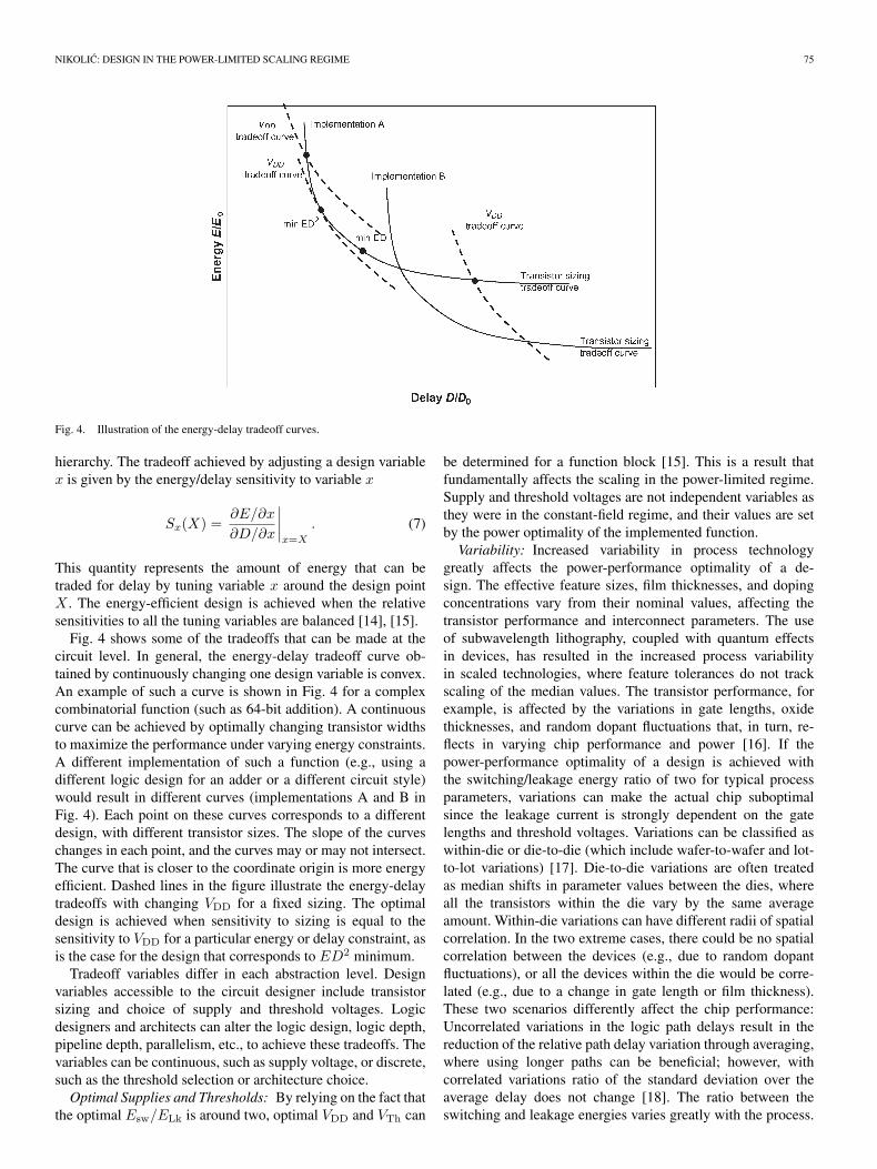
Fig. 4. Illustration of the energy-delay tradeoff curves.
hierarchy. The tradeoff achieved by adjusting a design variablex is given by the energy/delay sensitivity to variable x
Sx(X) =∂E/∂x
∂D/∂x
∣∣∣∣x=X
. (7)
This quantity represents the amount of energy that can betraded for delay by tuning variable x around the design pointX . The energy-efficient design is achieved when the relativesensitivities to all the tuning variables are balanced [14], [15].
Fig. 4 shows some of the tradeoffs that can be made at thecircuit level. In general, the energy-delay tradeoff curve ob-tained by continuously changing one design variable is convex.An example of such a curve is shown in Fig. 4 for a complexcombinatorial function (such as 64-bit addition). A continuouscurve can be achieved by optimally changing transistor widthsto maximize the performance under varying energy constraints.A different implementation of such a function (e.g., using adifferent logic design for an adder or a different circuit style)would result in different curves (implementations A and B inFig. 4). Each point on these curves corresponds to a differentdesign, with different transistor sizes. The slope of the curveschanges in each point, and the curves may or may not intersect.The curve that is closer to the coordinate origin is more energyefficient. Dashed lines in the figure illustrate the energy-delaytradeoffs with changing VDD for a fixed sizing. The optimaldesign is achieved when sensitivity to sizing is equal to thesensitivity to VDD for a particular energy or delay constraint, asis the case for the design that corresponds to ED2 minimum.
Tradeoff variables differ in each abstraction level. Designvariables accessible to the circuit designer include transistorsizing and choice of supply and threshold voltages. Logicdesigners and architects can alter the logic design, logic depth,pipeline depth, parallelism, etc., to achieve these tradeoffs. Thevariables can be continuous, such as supply voltage, or discrete,such as the threshold selection or architecture choice.Optimal Supplies and Thresholds: By relying on the fact that
the optimal Esw/ELk is around two, optimal VDD and VTh can
be determined for a function block [15]. This is a result thatfundamentally affects the scaling in the power-limited regime.Supply and threshold voltages are not independent variables asthey were in the constant-field regime, and their values are setby the power optimality of the implemented function.Variability: Increased variability in process technology
greatly affects the power-performance optimality of a de-sign. The effective feature sizes, film thicknesses, and dopingconcentrations vary from their nominal values, affecting thetransistor performance and interconnect parameters. The useof subwavelength lithography, coupled with quantum effectsin devices, has resulted in the increased process variabilityin scaled technologies, where feature tolerances do not trackscaling of the median values. The transistor performance, forexample, is affected by the variations in gate lengths, oxidethicknesses, and random dopant fluctuations that, in turn, re-flects in varying chip performance and power [16]. If thepower-performance optimality of a design is achieved withthe switching/leakage energy ratio of two for typical processparameters, variations can make the actual chip suboptimalsince the leakage current is strongly dependent on the gatelengths and threshold voltages. Variations can be classified aswithin-die or die-to-die (which include wafer-to-wafer and lot-to-lot variations) [17]. Die-to-die variations are often treatedas median shifts in parameter values between the dies, whereall the transistors within the die vary by the same averageamount. Within-die variations can have different radii of spatialcorrelation. In the two extreme cases, there could be no spatialcorrelation between the devices (e.g., due to random dopantfluctuations), or all the devices within the die would be corre-lated (e.g., due to a change in gate length or film thickness).These two scenarios differently affect the chip performance:Uncorrelated variations in the logic path delays result in thereduction of the relative path delay variation through averaging,where using longer paths can be beneficial; however, withcorrelated variations ratio of the standard deviation over theaverage delay does not change [18]. The ratio between theswitching and leakage energies varies greatly with the process.

76 IEEE TRANSACTIONS ON ELECTRON DEVICES, VOL. 55, NO. 1, JANUARY 2008
Estimating the leakage energy based on the process cornersonly would result in wide upper and lower bounds, separatedby more than an order of magnitude. To correctly center thedesign, it is necessary to include the estimation of distributionsof both die-to-die and within-die parameter variations [19].
Relative contributions of variability components and theirdistributions and correlations are generally unknown in ad-vance. In a 90-nm process, lithography-induced channel-lengthvariations dominate other sources; this, in turn, affects logicdelays and dramatically changes transistor leakage currents[20]. Reduction in device dimensions, along with the use ofrestricted design rules to control lithography-induced varia-tions, will increase the relative contribution of random dopantfluctuations because of smaller total dopant counts and canlikely become the dominant variability component in smalldevices [21]. While these variations will be averaged outin long logic paths, they may jeopardize the future of six-transistor SRAM.
To achieve a high product yield, designers add designmargins to both power and performance to accommodate themaximum process spread. These margins account for the worst-case process and do not distinguish between the die-to-dieand within-die contributions. As a result, the design is oftenpessimistic, with a large power penalty being paid to meet theperformance goals under the worst-case conditions.
In addition to process-induced variability, chip’s operationconditions and environment may vary. Changing input activitychanges the numbers of inactive logic gates, thus changingthe ratio of switching to leakage energy. Temperature dur-ing operation changes dramatically in some application areas,slowing down circuit performance and increasing leakage.Supply voltage noise may change with the environment as well,affecting the margins in the design.
III. EXAMPLES OF ENERGY-PERFORMANCE TRADEOFFS AT
CIRCUIT AND ARCHITECTURE LEVELS
Techniques for trading off energy and performance can bebroadly classified based on the time of their enable time and thetargeted energy components [22].
1) Enable time: some of the energy-performance tradeoffscan be implemented (or enabled) only at the design time,such as transistor sizing or the logic depth. On the otherhand, supply and threshold voltages can be either fixedduring the design phase or varied during run time. In thesleep mode, the performance does not matter (energy-delay sensitivity is zero), and the design variables areadjusted to minimize the energy.
2) Energy components: design techniques can primarilyaddress either dynamic (switching) or static (leakage)component of energy dissipation and trade them off forperformance. Lowering the supply voltage reduces bothswitching and leakage energies, while the adjustmentsin the threshold voltage primarily address the leakageenergy.
Numerous energy-saving techniques have been proposed inthe past. Usually, they are initially presented with the sole
purpose of energy reduction, without much discussion on theimpact on performance. For the purpose of this analysis, theyare classified in the following three categories.
1) Win–win techniques. The best techniques simultaneouslyincrease the performance and lower energy. These tech-niques are generally based on a major architectural oralgorithmic transformation and are often specific to aparticular application.
2) Zero or near-zero performance penalty. There are manytechniques that can lower energy with no impact onperformance. These techniques eliminate excess energyin the system, generally consumed in noncritical or re-dundant operations. Examples include the energy-delaytradeoffs in noncritical paths and clock gating techniques.Some of the techniques that reduce energy in variable-throughput applications are implemented with a verysmall overall performance cost.
3) True energy-performance tradeoffs. Majority of well-known LP techniques reduce the energy dissipation atthe expense of a lower system performance. Examplesof this include simply slowing down the circuits throughdownsizing, reducing the supply, or increasing thethreshold. Most techniques require an implementationoverhead that has to be accounted for in the performanceand energy budget.
Several known energy-saving techniques are evaluated in thissection, according to the classification in Table I, based on theenable time and performance impact, by roughly evaluatingtheir energy-performance sensitivities.
A. Reducing Switching Activity at the Design Time
There is a large body of work on reducing switching ac-tivity or total switched capacitance of circuits. Most notably,techniques include avoidance of unnecessary switching in time-multiplexed resources, exploiting correlation in signal process-ing data, algorithmic transformation, number representations,and reduction of bus activities [23]–[25]. Most of these tech-niques fall into categories 1) and 2). A particular exampleapplies in reducing the switching activity of clocks throughclock gating, which is a technique that deterministically turnsoff the clock to units or blocks that are not being active formultiple clock cycles. These techniques generally fall in thesecond category as their application does not incur any perfor-mance penalty, while the range of actual energy savings varieswith the application. One exception to this rule is the use offine-granularity clock gating, where the clock is automaticallygated by the data for every flip-flop (or a small group offlip-flops). This is implemented by comparing the new inputdatum to a flip-flop to its output; if they are the same, theclock edge is being absorbed [26]. This technique, because ofits fine granularity, has both the energy and the performanceoverhead, but can yield overall energy savings when selec-tively applied [27]. Clock gating and many of other switch-ing activity reduction techniques are well supported by theCAD tools.
NIKOLIC: DESIGN IN THE POWER-LIMITED SCALING REGIME 77
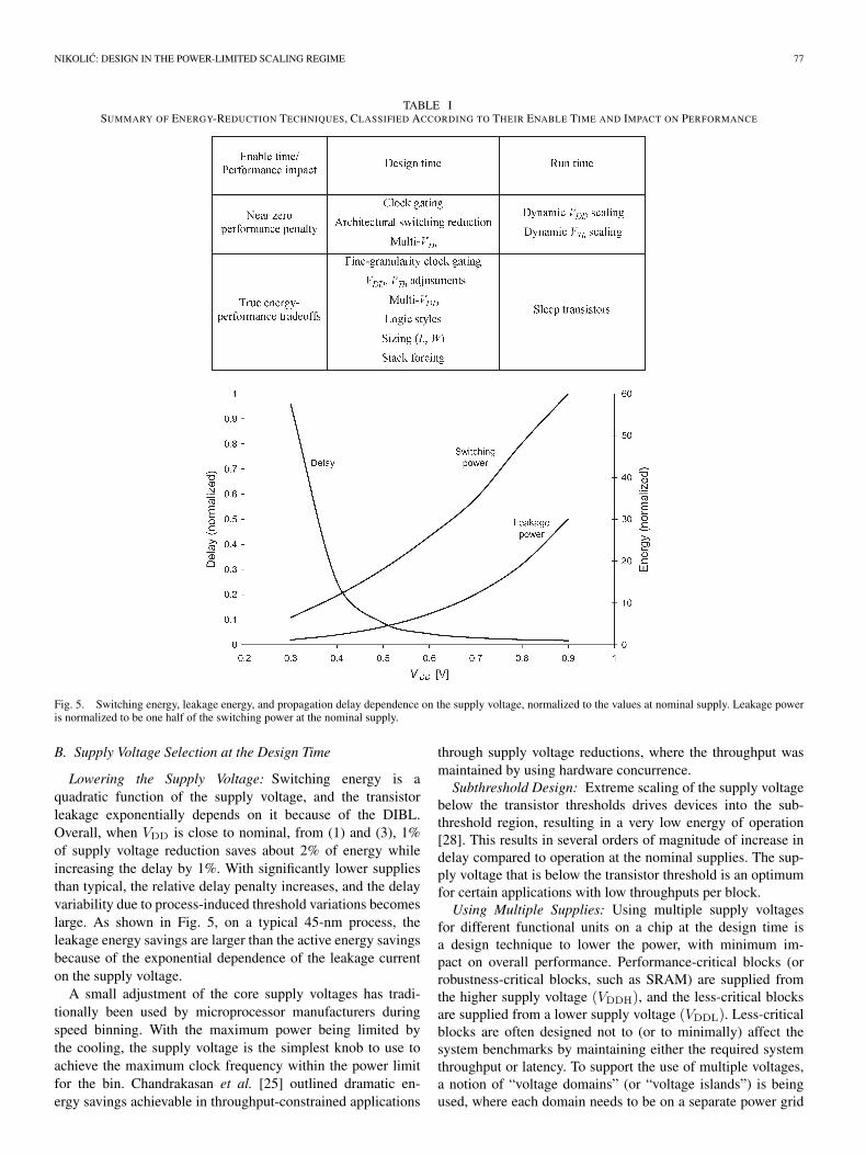
TABLE ISUMMARY OF ENERGY-REDUCTION TECHNIQUES, CLASSIFIED ACCORDING TO THEIR ENABLE TIME AND IMPACT ON PERFORMANCE
Fig. 5. Switching energy, leakage energy, and propagation delay dependence on the supply voltage, normalized to the values at nominal supply. Leakage poweris normalized to be one half of the switching power at the nominal supply.
B. Supply Voltage Selection at the Design Time
Lowering the Supply Voltage: Switching energy is aquadratic function of the supply voltage, and the transistorleakage exponentially depends on it because of the DIBL.Overall, when VDD is close to nominal, from (1) and (3), 1%of supply voltage reduction saves about 2% of energy whileincreasing the delay by 1%. With significantly lower suppliesthan typical, the relative delay penalty increases, and the delayvariability due to process-induced threshold variations becomeslarge. As shown in Fig. 5, on a typical 45-nm process, theleakage energy savings are larger than the active energy savingsbecause of the exponential dependence of the leakage currenton the supply voltage.
A small adjustment of the core supply voltages has tradi-tionally been used by microprocessor manufacturers duringspeed binning. With the maximum power being limited bythe cooling, the supply voltage is the simplest knob to use toachieve the maximum clock frequency within the power limitfor the bin. Chandrakasan et al. [25] outlined dramatic en-ergy savings achievable in throughput-constrained applications
through supply voltage reductions, where the throughput wasmaintained by using hardware concurrence.Subthreshold Design: Extreme scaling of the supply voltage
below the transistor thresholds drives devices into the sub-threshold region, resulting in a very low energy of operation[28]. This results in several orders of magnitude of increase indelay compared to operation at the nominal supplies. The sup-ply voltage that is below the transistor threshold is an optimumfor certain applications with low throughputs per block.Using Multiple Supplies: Using multiple supply voltages
for different functional units on a chip at the design time isa design technique to lower the power, with minimum im-pact on overall performance. Performance-critical blocks (orrobustness-critical blocks, such as SRAM) are supplied fromthe higher supply voltage (VDDH), and the less-critical blocksare supplied from a lower supply voltage (VDDL). Less-criticalblocks are often designed not to (or to minimally) affect thesystem benchmarks by maintaining either the required systemthroughput or latency. To support the use of multiple voltages,a notion of “voltage domains” (or “voltage islands”) is beingused, where each domain needs to be on a separate power grid

78 IEEE TRANSACTIONS ON ELECTRON DEVICES, VOL. 55, NO. 1, JANUARY 2008
Fig. 6. Level shifting from VDDL to VDDH. (a) Inverter-based. (b) Cross-coupled level converter. (c) Level-converting flip-flop.
Fig. 7. Normalized leakage current reduction in a general-purpose 45-nm technology. Sleep transistors reduce leakage by 25×, reverse bias reduces leakageby 3×, lower standby supply reduces leakage by 3–4×, and combined lower supply and reverse bias reduces leakage by 10×.
[29]. In addition, voltage levels of signals that are crossingthe domain boundaries have to be translated. A signal crossingover from a high-voltage domain into a low-voltage island doesnot require level conversion. However, when a signal fromthe low-voltage domain needs to drive a gate placed in thehigh-voltage domain, the pull-down networks in the CMOSgates have a lower overdrive, while the PMOS transistors arenot completely turned off, causing increased leakage in thatgate [Fig. 6(a)]. The signal level needs to be converted to thehigh-voltage level, which can be done using regenerative gates,such as a cross-coupled buffer, shown in Fig. 6(b); their addeddelay is the fundamental performance penalty for using thesecond supply. Because of the nature of the level converterdesign, it manifests higher sensitivity of the delay to processand voltage variations than the VDDL gates. Since the levelconversion can be conveniently performed both logically andphysically at the input of the VDDL block, it can be associated
with the timing boundary and incorporated into a flip-flop, andan example of such a design is shown in Fig. 6(c) [30]. Theuse of voltage domains is well supported in the contemporarydesign flows. Practical limitations in generating and distributingsupply voltages often limit the number of voltages to two.
By taking the idea of using multiple supplies further, it canbe envisioned to use them inside a combinational logic block[31]. To implement this idea, level conversion is necessary forevery crossing of a signal from VDDL to VDDH. To simplifythe implementation and to minimize its delay sensitivity todisturbances, the idea of clustered voltage scaling can be used,where only one transition from VDDH to VDDL is allowedfor each logic path, and the level conversion, if necessary, isperformed in the flip-flops. This requires VDDH gates to beclustered in the beginning of each path and simplifies the supplyassignment task for each gate. However, the use of two sup-ply voltages, whether implemented in custom or standard-cell

NIKOLIC: DESIGN IN THE POWER-LIMITED SCALING REGIME 79
Fig. 8. Impact of a slow down of noncritical paths on the delay distribution ofa logic block.
design methodology, requires changes in placement of gates.Using two power rails within the cell is one way of dis-tributing two supplies. Although this has been demonstratedin a custom datapath [32], it is impractical for standard celldesigns because of the need for well spacing, increased cellheight, and blockages introduced by using low metal layers(M2) for power routing. A practical solution for distribution ofpower supplies in dual supply blocks is by alternating VDDH
and VDDL rows [31]. Overall, the dual supply design saves15%–35% of energy, excluding the cost of supply generationwith minimal delay penalty [30]. Although attractive, thesesavings are not significant enough to promote the commercialuse of this technique because of added design complexity, lackof CAD support, and decreased robustness.
C. Dynamic Energy Management
Dynamic Voltage Scaling (DVS): Most real-time systems aredesigned to meet maximum throughput requirements in theworst case, but their actual computing requirements greatlyvary in time. A general-purpose processor to be used in portableapplications, such as notebook computers, electronic organiz-ers, and mobile phones, executes computational functions thatfall into three major categories: compute-intensive tasks, low-throughput/high-latency functions, and idle-mode operation.Compute-intensive and short-latency tasks need the full com-putational throughput of the processor to achieve real-timeconstraints. MPEG video compression and decompression, orinteractive gaming, are examples of such. Low-throughput andlong-latency tasks, such as text processing or data entry, operateunder far more relaxed completion deadlines and require onlya fraction of the maximum processor’s throughput. There isno reward for finishing the computation early, and if a taskis completed early, it can be considered as a waste of energy.Finally, portable processors spend a large fraction of their timein the idle mode, waiting for a user action or an external event.
Even compute-intensive operations, such as MPEG decod-ing, show variable computational requirements while process-ing a typical stream of data. For example, the number oftimes an MPEG decoder computes an inverse discrete cosinetransform per video frame varies widely depending upon theamount of motion in the video scenes [34].
By simultaneously lowering the operating frequency and thesupply voltage while executing low-throughput/high-latencyload, switching energy is quadratically lowered. In order tomaintain the required throughput for high workloads and min-
imize energy for low workloads, both supply and frequencymust be dynamically varied according to the requirementsapplication that is currently being executed. This techniqueis called the DVS and is implemented such that the func-tion is operated at the lowest supply voltage that meets thetiming constraints [33]–[35]. For successful implementationof this technique, it is necessary to monitor the variation ofthe critical path delay with supply voltage. Various CMOScircuit delays generally track each other with scaling of thesupply voltage [33]. In the simplest implementation, the delayis monitored through a simple ring oscillator that presentsa replica of the critical path, with a sufficient margin [33].Circuits exhibit relative delay variations depending if theyare gate-capacitance dominated, diffusion dominated, and wiredominated. To lower the design margin in monitoring, it isnecessary to observe replicas of different critical paths, whichmight end up reordered in criticality with supply and processvariations [37].
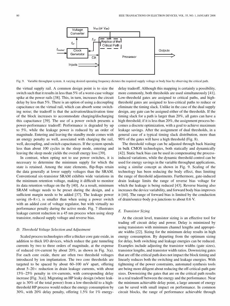
A practical DVS system, shown in Fig. 9, consists of thefollowing components:
1) a circuit block that can operate under a wide variety ofsupply voltages;
2) a supply-regulation loop that sets the minimum voltagenecessary for operation at a desired frequency;
3) an operating system and scheduler that calculates therequired frequencies to meet requested throughputs andtask completion deadlines.
A monitored delay is included in the power-supply controlloop to provide the translation between the supply voltage andthe clock frequency. The operating system digitally sets thedesired operating cycle time, and the current value of the delaymonitor is compared against it. The difference is used as afeedback error. By adjusting the supply voltage, the supplyvoltage loop changes the delay to set this error value to zero,incurring no performance penalty. A small performance hitmay exist during the transition from one mode of operationto another as it may take several clock cycles to ramp up thesupply voltage.Standby Power Management: Many systems spend most of
the time in the standby mode, waiting for an external or internalevent to respond to. In order to save energy, it is desirable tooperate at the minimum possible supply voltage in the standby.Turning off the supply is not always permissible in the system.The state of the block is erased when the supply is OFF, andrestarting the system may take a long time. Furthermore, it isdifficult to implement a perfect electronic in-line CMOS switch,which has zero ON-resistance and OFF-current. In standard tech-nologies, this switch is implemented as a thick-oxide longer-channel-length NMOS or PMOS transistor, with associateddesign tradeoffs. Using higher thresholds and longer channellengths suppresses the leakage currents through the switch [36].To further suppress leakage currents, when a negative supply isavailable, it can be applied to the gate of the switch. The switchneeds to have minimal series resistance; this can be accom-plished by increasing its size, lowering the threshold, or increas-ing the gate voltage if the higher voltage is available. The switchresistance is usually targeted to minimize the voltage noise on
80 IEEE TRANSACTIONS ON ELECTRON DEVICES, VOL. 55, NO. 1, JANUARY 2008
Fig. 9. Variable throughput system. A varying desired operating frequency dictates the required supply voltage or body bias by observing the critical path.
the virtual supply rail. A common design point is to size theswitch such that it results in less than 5% of a worst-case voltagespike at the power rails [38]. This, in turn, increases the circuitdelay by less than 5%. There is an option of using a decouplingcapacitance on the virtual rail, which can absorb some switch-ing noise; the tradeoff is that the activation/deactivation timeof the block increases to accommodate charging/dischargingthis capacitance [39]. The use of a power switch presents apower-performance tradeoff: Performance is degraded by upto 5%, while the leakage power is reduced by an order ofmagnitude. Entering and leaving the standby mode comes withan energy penalty as well, associated with charging the rail,well, decoupling, and switch capacitances. If the system spendsless than about 100 cycles in the sleep mode, entering andleaving the sleep mode yields the overall energy loss [39].
In contrast, when opting not to use power switches, it isnecessary to determine the minimum supply for which thestate is retained. Among the state elements, flip-flops retainthe data generally at lower supply voltages than the SRAM.Conventional six-transistor SRAM exhibits wide variations inthe minimum retention voltage, making it difficult to monitorits data retention voltage on the fly [40]. As a result, minimumSRAM voltage needs to be preset during the design, and asufficient margin needs to be added [37]. The leakage powersaving (6–8×), is smaller than when using a power switchwith an added cost of voltage regulator, but with virtually noperformance penalty during the active mode. Fig. 7 illustratesleakage current reduction in a 45 nm process when using sleeptransistor, reduced supply voltage and reverse bias.
D. Threshold Voltage Selection and Adjustment
Scaled process technologies offer a thicker core gate oxide, inaddition to thick I/O devices, which reduce the gate tunnelingcurrents by two to three orders of magnitude, at the expenseof reduced ON-current by about 20%, as shown in Fig. 3(a).For each core oxide, there are often two threshold voltagesintroduced by ion implantation. The two core thresholds aretargeted to be spaced by about 60–100 mV apart, offeringabout 5–20× reduction in drain leakage currents, with about15%–25% penalty in ON-currents, with corresponding delayincrease [Fig. 3(a)]. Migrating an HP leaky design (where leak-age is 30% of the total power) from a low-threshold to a high-threshold HP process would reduce the energy consumption by30%, with 20% delay penalty, offering 1.5% for 1% energy-
delay tradeoff. Although this mapping is certainly a possibility,more commonly, both thresholds are used simultaneously [41].Low-threshold gates are assigned to critical paths, and high-threshold gates are assigned to less-critical paths to reduce oreliminate the timing slack. Unlike in the case of the dual supplydesign, any gate can be assigned either of the thresholds. If thetiming slack for a path is larger than 20%, all gates can have ahigh threshold; if it is less than 20%, the assignment process be-comes a discrete optimization, with a goal to achieve maximumleakage savings. After the assignment of dual thresholds, in ageneral case of a typical timing slack distribution, more than90% of the gates will have a high threshold (Fig. 8).
The threshold voltage can be adjusted through back biasingin bulk CMOS technologies, both statically and dynamically[42]. Static back bias can be used in compensating the process-induced variations, while the dynamic threshold control can beused for energy savings in the variable throughput applications,using a similar concept as shown in Fig. 9. Scaling of thetechnology has been reducing the body effect, thus limitingthe range of threshold adjustments. Furthermore, gate-induceddrain leakage limits the range of reverse bias voltage forwhich the leakage is being reduced [43]. Reverse biasing alsoincreases the device variability, and forward body bias improvesit [44]. The range of forward bias is limited by the conductionof drain/source-body p-n junctions to about 0.6 V.
E. Transistor Sizing
At the circuit level, transistor sizing is an effective tool fortrading off circuit delay and power. Delay is minimized byusing transistors with minimum channel lengths and appropri-ate widths [22]. Sizing for the minimum delay results in highenergy consumption. By departing from the optimum sizingfor delay, both switching and leakage energies can be reduced.Examples include adjusting the transistor widths (gate sizes),transistor lengths, and transistor width ratios. Downsizing gatesthat are off the critical path does not impact the block timing andlinearly reduces both the switching and leakage energies. Withtightening of the power constraints, automated synthesis toolsare being more diligent about reducing the off-critical-path gatesizes. Downsizing the gates that are on the critical path resultsin a real tradeoff between the energy and the performance. Nearthe minimum achievable delay point, a large amount of energycan be saved with small impact on performance. In commoncircuit blocks, the range of performance achievable through
NIKOLIC: DESIGN IN THE POWER-LIMITED SCALING REGIME 81
sizing is about 2×, where the fastest circuit has about a halfof the delay of a minimum-sized one, while the range of energycould vary widely. The sensitivity varies from a very large valuedown to zero [15].
Increasing the transistor channel lengths reduces the leakage,but increases the gate capacitance, which, in turn, increasesswitching power and impacts the delay. In a general-purpose45-nm process, with standard device thresholds, increasing thegate length from the minimum by 5 nm (which is a commonmanufacturing grid in sub-100-nm technologies) reduces theleakage current by 4–5× across process corners. If the W/Lratio is preserved, the drive current is reduced by 3.6%, andthe input capacitance is increased quadratically (26%), thusslowing down the preceding gate. When placed in a criticalpath and normalized, the transistor length increase of about10% decreases the leakage by 4000%, increases the delay byabout 30%, and increases the active power by about 25%.The overall effectiveness of this technique largely depends onthe fraction of the leakage in the original design. For designswhere the leakage contributes more than 25% of the overallpower budget, there is an overall win in power savings. Forexample, if a design dissipates 30% of leakage power, the netbalance is that 1% of delay penalty saves about 0.7% of theenergy. Assuming that the gate is off the critical path and thatcan be slowed down just by increasing the transistor lengthor decreasing the gate width, adjusting gate lengths becomesmore effective when leakage contributes more than 25% of thetotal power.
Leakage reduction is very steep near the minimum channellength, potentially offering an attractive technique to achievelarge leakage energy savings with linear switching power in-crease, by slightly increasing transistor lengths of gates thatare off the critical path [45]. This cannot be done in thedesign phase as the transistor lengths are usually restrictedto be placed on a manufacturing grid that is 5 nm or more.However, smaller channel-length biases (less than 10%) canbe made directly in the mask layouts, making this approachpossible [46].
F. Transistor Stacks
Stacking transistors is another way of trading off activepower and delay for leakage power savings [47], besides theuse in the sleep mode. For example, a stack of two OFF devicesin 45-nm CMOS leaks about 25× less than a single device.Adding the third OFF-transistor to the stack reduces the leakageby another factor of two, resulting in a net leakage that is 50×smaller than the leakage of a single transistor.
Transistor stacks occur naturally in CMOS logic—a two-input NAND gate has a stack of two NMOS transistors. Toreduce the leakage in the sleep mode, both transistors in thestack should be OFF; however, bringing the logic block intoa state where all the appropriate signals are set for minimumleakage may take several clock cycles.
Stacks can be forced when needed by adding another tran-sistor in the stack [47]. Adding an NMOS transistor to thestack in the inverter reduces the leakage by 25×, and withoutincreasing the transistor width, it doubles the input capacitance
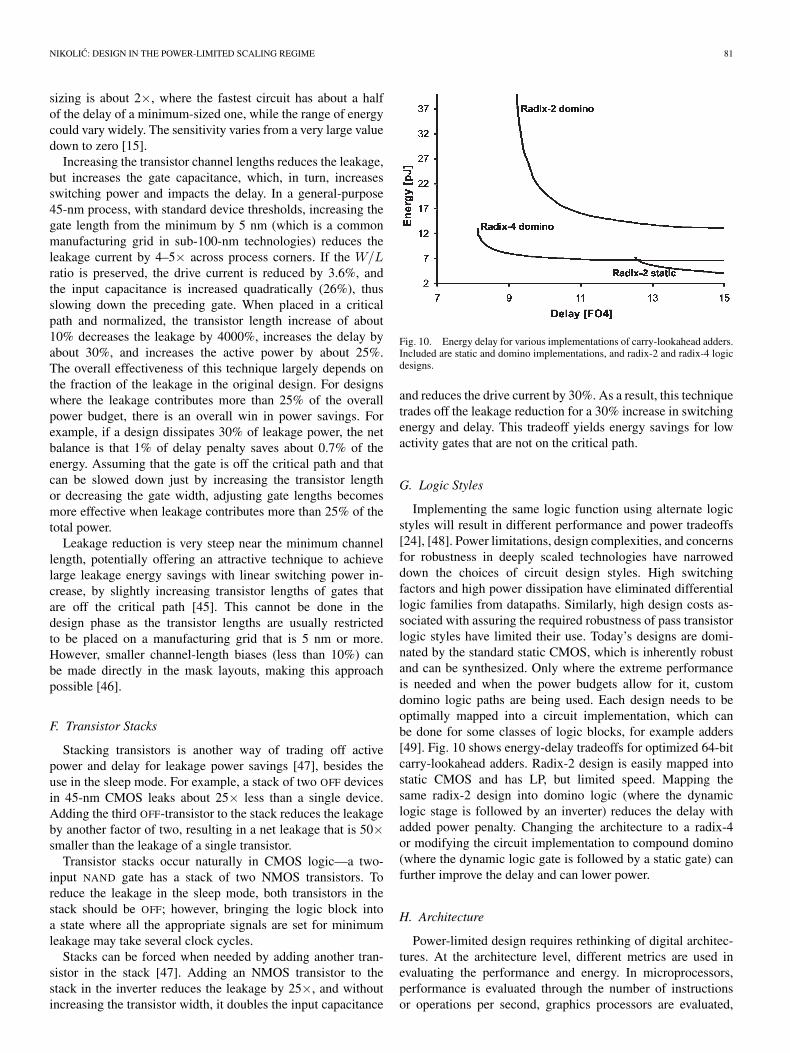
Fig. 10. Energy delay for various implementations of carry-lookahead adders.Included are static and domino implementations, and radix-2 and radix-4 logicdesigns.
and reduces the drive current by 30%. As a result, this techniquetrades off the leakage reduction for a 30% increase in switchingenergy and delay. This tradeoff yields energy savings for lowactivity gates that are not on the critical path.
G. Logic Styles
Implementing the same logic function using alternate logicstyles will result in different performance and power tradeoffs[24], [48]. Power limitations, design complexities, and concernsfor robustness in deeply scaled technologies have narroweddown the choices of circuit design styles. High switchingfactors and high power dissipation have eliminated differentiallogic families from datapaths. Similarly, high design costs as-sociated with assuring the required robustness of pass transistorlogic styles have limited their use. Today’s designs are domi-nated by the standard static CMOS, which is inherently robustand can be synthesized. Only where the extreme performanceis needed and when the power budgets allow for it, customdomino logic paths are being used. Each design needs to beoptimally mapped into a circuit implementation, which canbe done for some classes of logic blocks, for example adders[49]. Fig. 10 shows energy-delay tradeoffs for optimized 64-bitcarry-lookahead adders. Radix-2 design is easily mapped intostatic CMOS and has LP, but limited speed. Mapping thesame radix-2 design into domino logic (where the dynamiclogic stage is followed by an inverter) reduces the delay withadded power penalty. Changing the architecture to a radix-4or modifying the circuit implementation to compound domino(where the dynamic logic gate is followed by a static gate) canfurther improve the delay and can lower power.
H. Architecture
Power-limited design requires rethinking of digital architec-tures. At the architecture level, different metrics are used inevaluating the performance and energy. In microprocessors,performance is evaluated through the number of instructionsor operations per second, graphics processors are evaluated,

82 IEEE TRANSACTIONS ON ELECTRON DEVICES, VOL. 55, NO. 1, JANUARY 2008
e.g., by the number of vertices processed per second, and sig-nal processors have their own application-dependent aggregateperformance metrics. Finally, the system performance is mea-sured by a common benchmark score.
Energy and performance can be effectively traded off atthe system level by increasing the level of concurrency in theexecution, which involves tradeoffs in the number of functionalunits and their organization. Concurrency can also be increasedby increasing the depth of pipelining or parallelism withina functional unit. Increasing concurrency often results in in-creased chip area, thus increasing the system cost. To establishthe relationship between the performance and energy, syntheticmetrics can be used, such as energy and area efficiencies,defined as the number of operations per unit of energy and theunit of area, respectively.
A classical example of an interaction of a higher level ar-chitectural design variable, such as the degree of parallelism orpipelining, with a technology design variable, such as a supplyvoltage, has been studied in [25]. By using parallelism or deeperpipelining, a datapath can have the same throughput at a lowersupply voltage, reducing the active power dissipation. Withoptimized transistor thresholds and supplies, parallelism andpipelining reduce the total power. It is important to point outthat, because of a larger number of inactive circuits in paralleldatapaths, optimal thresholds in parallel datapaths are higherthan in pipelined. The ultimate benefit of increased concurrencyimplemented through parallelism or pipelining is limited bypractical constraints, like the minimum practical supply voltageor logic depth, and on the range of energy-delay tradeoffs forimplementing the desired function.
Architectural changes can have a very large impact on powerdissipation of a system, and power-conscious rearchitecting ofa system might be able to improve the performance. Micro-processors in the past have been increasing the pipeline depthwhile reducing the logic depth to about 10–15 to increasethe performance through increasing the clock frequency, at adramatic cost in power. Power-limited designs prefer somewhatdeeper logic. In an example study, it has been shown that thelogic depth of 22 FO4 inverters is optimal for PowerPC ar-chitecture [50]. Practical trends in mainstream microprocessorshave followed this trend as well. Intel has backed off fromthe Pentium 4 architecture and opted for longer logic pathsin multicore processors. Modern processors utilize multipleprocessor cores and larger cache memories, operating at lowersupplies.
IV. CONCLUSION
Today, power limitations are as important in the design as isthe performance. Design in the power-limited-scaling regimerequires continuous changes in the architectures, circuit im-plementation, and technology choices to maximize the perfor-mance under power constraints. Many techniques for loweringpower consumption are well known, but their implementationoften incurs a performance penalty. An optimum implemen-tation is achieved when the energy/delay sensitivity of thedesign is equal for all the design and technology variables.Implementation of LP techniques increases the design and
verification complexity and often requires special technologyfeatures, which increases the design cost. Ultimately, scalingwill end when the increase in the design cost stops beingmanageable.
ITRS recognizes the emerging device structures as possi-ble candidates in replacing planar CMOS device structures.Double-gate transistors offer better OFF-currents, and if thevelocity enhancement techniques are applied, it offers betterON-currents as well. Their application in circuit design favor-ably shifts the basic energy-performance tradeoff curves (butdoes not fundamentally alter them), which would provide a one-time performance boost/energy reduction at the point of theirintroduction.
ACKNOWLEDGMENT
The author would like to thank the students, faculty,and sponsors of the Berkeley Wireless Research Center fortheir contributions and D. Markovic, V. Stojanovic, andR. Zlatanovici, in collaboration with M. Horowitz andR. Brodersen, for the sensitivity-based optimization.
REFERENCES
[1] R. H. Dennard, F. H. Gaensslen, V. L. Rideout, E. Bassous, andA. R. LeBlanc, “Design of ion-implanted MOSFETs with very smallphysical dimensions,” IEEE J. Solid-State Circuits, vol. SSC-9, no. 5,pp. 256–268, Oct. 1974.
[2] S. Borkar, “Design challenges of technology scaling,” IEEE Micro,vol. 19, no. 4, pp. 23–29, Jul./Aug. 1999.
[3] P. P. Gelsinger, “Microprocessors for the new millennium: Challenges,opportunities and the new frontiers,” in Proc. ISSCC Dig. Tech. Papers,San Francisco, CA, Feb. 5–7, 2001, pp. 22–25.
[4] K. Toh, P. Ko, and R. Meyer, “An engineering model for short-channelMOS devices,” IEEE J. Solid-State Circuits, vol. 23, no. 4, pp. 950–958,Aug. 1988.
[5] Y. Taur and T. H. Ning, Fundamentals of Modern VLSI Devices.Cambridge, U.K.: Cambridge Univ. Press, 1998.
[6] H. J. M. Veendrick, “Short-circuit dissipation of static CMOS circuitryand its impact on the design of buffer circuits,” IEEE J. Solid-StateCircuits, vol. SSC-19, no. 4, pp. 468–473, Aug. 1984.
[7] Intel’s Transistor Technology Breakthrough Represents Biggest Changeto Computer Chips in 40 Years, Jan. 2007. Intel Corp., press release.[Online]. Available: http://www.intel.com/pressroom/archive/releases/20070128comp.htm
[8] IBM Advancement to Spawn New Generation of Chips, Jan. 2007.IBM Corp., press release. [Online]. Available: http://www-03.ibm.com/press/us/en/pressrelease/20980.wss
[9] J. Burr and A. M. Peterson, “Ultra low power CMOS technology,” in Proc.NASA VLSI Des. Symp., Oct. 1991, pp. 4.2.1–4.2.13.
[10] R. Gonzalez, B. Gordon, and M. A. Horowitz, “Supply and thresholdvoltage scaling for low power CMOS,” IEEE J. Solid-State Circuits,vol. 32, no. 8, pp. 1210–1216, Aug. 1997.
[11] K. Nose and T. Sakurai, “Optimization of VDD and VTH for low-powerand high-speed applications,” in Proc. Asia South Pacific Des. Autom.Conf., Jan. 2000, pp. 469–474.
[12] International Technology Roadmap for Semiconductors, 2006. [Online].Available: http://public.itrs.net
[13] A. J. Martin, “Towards an energy complexity of computation,” Inf.Process. Lett., vol. 77, no. 2–4, pp. 181–187, Feb. 2001.
[14] V. Zyuban et al., “Integrated analysis of power and performance forpipelined microprocessors,” IEEE Trans. Comput., vol. 53, no. 8,pp. 1004–1016, Aug. 2004.
[15] D. Markovic, V. Stojanovic, B. Nikolic, M. A. Horowitz, andR. W. Brodersen, “Methods for true energy-performance optimization,”IEEE J. Solid-State Circuits, vol. 39, no. 8, pp. 1282–1293, Aug. 2004.
[16] K. Bernstein et al., “High-performance CMOS variability in the 65-nmregime and beyond,” IBM J. Res. Develop., vol. 50, no. 4/5, pp. 433–450,Jul.–Sep. 2006.

NIKOLIC: DESIGN IN THE POWER-LIMITED SCALING REGIME 83
[17] J. W. Tschanz et al., “Adaptive body bias for reducing impacts of die-to-die and within-die parameter variations on microprocessor frequency andleakage,” IEEE J. Solid-State Circuits, vol. 37, no. 11, pp. 1396–1402,Nov. 2002.
[18] K. A. Bowman, S. G. Duvall, and J. D. Meindl, “Impact of die-to-die andwithin-die parameter fluctuations on the maximum clock frequency dis-tribution for gigascale integration,” IEEE J. Solid-State Circuits, vol. 37,no. 2, pp. 183–190, Feb. 2002.
[19] S. Narendra, V. De, S. Borkar, D. A. Antoniadis, and A. P. Chandrakasan,“Full-chip subthreshold leakage power prediction and reduction tech-niques for sub-0.18-µm CMOS,” IEEE J. Solid-State Circuits, vol. 39,no. 3, p. 510, Mar. 2004.
[20] L. T. Pang and B. Nikolic, “Impact of layout on 90 nm CMOS processparameter fluctuations,” in Proc. Symp. VLSI Circuits, Dig. Tech. Papers,Honolulu, HI, Jun. 15–17, 2006, pp. 84–85.
[21] D. J. Frank, R. H. Dennard, E. Nowak, P. M. Solomon, Y. Taur, andH.-S. P. Wong, “Device scaling limits of Si MOSFETs and theirapplication dependencies,” Proc. IEEE, vol. 89, no. 3, pp. 259–288,Mar. 2001.
[22] J. M. Rabaey, A. Chandrakasan, and B. Nikolic, Digital IntegratedCircuits: A Design Perspective, 2nd ed. Upper Saddle River, NJ:Prentice-Hall, 2003.
[23] A. P. Chandrakasan, M. Potkonjak, R. Mehra, J. Rabaey, andR. W. Brodersen, “Optimizing power using transformations,” IEEE Trans.Comput.-Aided Design Integr. Circuits Syst., vol. 14, no. 1, pp. 12–31,Jan. 1995.
[24] A. P. Chandrakasan and R. W. Brodersen, “Minimizing power consump-tion in digital CMOS circuits,” Proc. IEEE, vol. 83, no. 4, pp. 498–523,Apr. 1995.
[25] A. P. Chandrakasan, S. Sheng, and R. W. Brodersen, “Low-power CMOSdigital design,” IEEE J. Solid-State Circuits, vol. 27, no. 4, pp. 473–484,Apr. 1992.
[26] M. Hamada et al., “Flip-flop selection technique for power-delaytrade-off,” in Proc. IEEE Int. Solid-State Circuits Conf., Dig. Tech.Papers, San Francisco, CA, Feb. 15–17, 1999, pp. 270–271.
[27] D. Markovic, B. Nikolic, and R. W. Brodersen, “Analysis and design oflow-energy flip-flops,” in Proc. ACM/IEEE ISLPED, Huntington Beach,CA, Aug. 6–7, 2001, pp. 52–55.
[28] B. H. Calhoun, A. Wang, and A. Chandrakasan, “Modeling and sizing forminimum energy operation in subthreshold circuits,” IEEE J. Solid-StateCircuits, vol. 40, no. 9, pp. 1778–1786, Sep. 2005.
[29] D. E. Lackey, P. S. Zuchowski, T. R. Bednar, D. W. Stout, S. W. Gould,and J. M Cohn, “Managing power and performance for system-on-chipdesigns using voltage islands,” in Proc. IEEE/ACM ICCAD, San Jose,CA, Nov. 10–14, 2002, pp. 195–202.
[30] F. Ishihara, F. Sheikh, and B. Nikolic, “Level-conversion for dual-supplysystems,” IEEE Trans. Very Large Scale Integr. (VLSI) Syst., vol. 12, no. 2,pp. 185–195, Feb. 2004.
[31] K. Usami and M. Horowitz, “Clustered voltage scaling technique for low-power design,” in Proc. Int. Symp. Low Power Des., Dana Point, CA,Apr. 23–26, 1995, pp. 3–8.
[32] Y. Shimazaki, R. Zlatanovici, and B. Nikolic, “A shared-well dual-supply-voltage 64-bit ALU,” IEEE J. Solid-State Circuits, vol. 39, no. 3, pp. 494–500, Mar. 2004.
[33] T. D. Burd, T. A. Pering, A. J. Stratakos, and R. W. Brodersen, “Adynamic voltage scaled microprocessor system,” IEEE J. Solid-StateCircuits, vol. 35, no. 11, pp. 1571–1580, Nov. 2000.
[34] V. Gutnik and P. Chandrakasan, “Embedded power supply for low-powerDSP,” IEEE Trans. Very Large Scale Integr. (VLSI) Syst., vol. 5, no. 4,pp. 425–435, Dec. 1997.
[35] T. Kuroda et al., “Variable supply-voltage scheme for low-power high-speed CMOS digital design,” IEEE J. Solid-State Circuits, vol. 33, no. 3,pp. 454–462, Mar. 1998.
[36] S. Mutoh, T. Douseki, Y. Matsuya, T. Aoki, S. Shigematsu, andJ. Yamada, “1-V power supply high-speed digital circuit technology withmultithreshold-voltage CMOS,” IEEE J. Solid-State Circuits, vol. 30,no. 8, pp. 847–854, Aug. 1995.
[37] H. Mair, “A 65-nm mobile multimedia applications processor with anadaptive power management scheme to compensate for variations,” inProc. Symp. VLSI Circuits, Honolulu, HI, Jun. 2007, pp. 224–225.
[38] J. Kao, A. Chandrakasan, and D. Antoniadis, “Transistor sizing issues andtool for multi-threshold CMOS technology,” in Proc. 34th Des. Autom.Conf., Jun. 1997, pp. 409–414.
[39] J. W. Tschanz, S. G. Narendra, Y. Ye, B. A. Bloechel, S. Borkar, andV. De, “Dynamic sleep transistor and body bias for active leakage powercontrol of microprocessors,” IEEE J. Solid-State Circuits, vol. 38, no. 11,pp. 1838–1845, Nov. 2003.
[40] H. Qin, Y. Cao, D. Markovic, A. Vladimirescu, and J. Rabaey, “SRAMleakage suppression by minimizing standby supply voltage,” in Proc. 5thInt. Symp. Quality Electron. Des., 2004, pp. 55–60.
[41] L. Wei, Z. Chen, K. Roy, Y. Ye, and V. De, “Mixed-Vth (MVT) CMOScircuit design methodology for low power applications,” in Proc. 36thDes. Autom. Conf., Jun. 1999, pp. 430–435.
[42] T. Kuroda et al., “A 0.9-V, 150-MHz, 10-mW, 4 mm2, 2-D discrete cosinetransform core processor with variable threshold-voltage (VT) scheme,”IEEE J. Solid-State Circuits, vol. 31, no. 11, pp. 1770–1779, Nov. 1996.
[43] A. Keshavarzi, S. Narendra, S. Borkar, C. Hawkins, K. Roy, and V. De,“Technology scaling behavior of optimum reverse body bias for standbyleakage power reduction in CMOS IC’s,” in Proc. Int. Symp. Low PowerElectron. Des., Aug. 1999, pp. 252–254.
[44] J. Tschanz et al., “Adaptive body bias for reducing impacts of die-to-die and within-die parameter variations on microprocessor frequency andleakage,” IEEE J. Solid-State Circuits, vol. 37, no. 11, pp. 1396–1402,Nov. 2002.
[45] S. Rusu et al., “A 65-nm dual-core multithreaded Xeon processor with16-MB L3 cache,” IEEE J. Solid-State Circuits, vol. 42, no. 1, pp. 17–25,Jan. 2007.
[46] P. Gupta, A. B. Kahng, P. Sharma, and D. Sylvester, “Gate-length biasingfor runtime-leakage control,” IEEE Trans. Comput.-Aided Design Integr.Circuits Syst., vol. 25, no. 8, pp. 1475–1485, Aug. 2006.
[47] S. Narendra, S. Borkar, V. De, D. Antoniadis, and A. Chandrakasan,“Scaling of stack effect and its application for leakage reduction,” in Proc.Int. Symp. Low Power Electron. Des., Aug. 2001, pp. 195–200.
[48] S. Kosonocky et al., “Low power circuits and technology for wirelessdigital systems,” IBM J. Res. Develop., vol. 47, no. 2/3, pp. 283–298,Mar.–May 2003.
[49] S. Kao, R. Zlatanovici, and B. Nikolic, “A 250 ps 64-bit carry-lookaheadadder in 90 nm CMOS,” in Proc. IEEE ISSCC, Dig. Tech. Papers, SanFrancisco, CA, Feb. 4–8, 2006, pp. 438–439.
[50] V. Srinivasan et al., “Optimizing pipelines for power and performance,”in Proc. 35th Annu. IEEE/ACM Int. Symp. Microarchitecture, (MICRO),Nov. 2002, pp. 333–344.
Borivoje Nikolic (S’93–M’99–SM’06) received theDipl.Ing. and M.Sc. degrees in electrical engineeringfrom the University of Belgrade, Belgrade, Serbia,in 1992 and 1994, respectively, and the Ph.D. degreefrom the University of California at Davis, Davis,in 1999.
He was with the faculty of the University ofBelgrade from 1992 to 1996. He spent two yearswith Silicon Systems, Inc., Texas Instruments Stor-age Products Group, San Jose, CA, working ondisk-drive signal processing electronics. In 1999,
he joined the Department of Electrical Engineering and Computer Sciences,University of California at Berkeley, Berkeley, where he is now an AssociateProfessor. His research activities include high-speed and low-power digitalintegrated circuits and VLSI implementation of communications and signalprocessing algorithms. He is the coauthor of Digital Integrated Circuits: ADesign Perspective, 2nd ed. (Prentice-Hall, 2003).
Dr. Nikolic received the IBM Faculty Partnership Award in 2005–2007, NSFCAREER award in 2003, College of Engineering Best Doctoral DissertationPrize, and Anil K. Jain Prize for the Best Doctoral Dissertation in Electrical andComputer Engineering, University of California at Davis, in 1999, as well as theCity of Belgrade Award for the Best Diploma Thesis in 1992. For works withhis students and colleagues, he received the Best Paper Award at the ACM/IEEEInternational Symposium of Low-Power Electronics in 2005 and the 2004 JackKilby Award for the Outstanding Student Paper at the IEEE International Solid-State Circuits Conference.