ieee transactions on electron devices, vol. 63, no. 1...
TRANSCRIPT

IEEE TRANSACTIONS ON ELECTRON DEVICES, VOL. 63, NO. 1, JANUARY 2016 223
III–V Nanowire Transistors for Low-Power LogicApplications: A Review and Outlook
Chen Zhang, Member, IEEE, and Xiuling Li, Senior Member, IEEE
(Review Paper)
Abstract— III–V semiconductors, especially InAs, have muchhigher electron mobilities than Si and have been considered aspromising candidates for n-channel materials for post-Si low-power CMOS logic applications. Combined with the inherent3-D structure that enables the gate-all-around (GAA) geometryfor superb gate electrostatic control, III–V nanowire (NW) MOS-FETs are well positioned to extend the scaling beyond Si. Thispaper attempts to provide a review of the growth and fabricationapproaches (both bottom–up and top–down), and the state-of-the-art device performance of III-V NW GAA MOSFETs, as well asan outlook of their scaling potential.
Index Terms— III–V, gate-all-around (GAA), MOSFET,nanowire (NW), scaling.
I. INTRODUCTION
III–V SEMICONDUCTOR materials, especially InAs,are known to have a much higher electron mobil-
ity than Si [1]–[3]. For extremely scaled FETs, the highmobility is translated to high source-side carrier injectionvelocity [3]–[5]. III–V transistors, therefore, have been widelyused for high-speed and RF electronic applications fordecades. Record high-frequency performances have beenachieved using III–V channels [6]–[8]. Recently, attentionhas been drawn on the potential of III–V materials for logicdevice applications [3], [9]–[11], which has historically beenthe territory of Si. The continuous performance improvementof Si CMOS ICs over the past 40 years has been enabledby aggressive downscaling of the transistor size, as well asthe increase of operating frequency, with the enhancement ofpower density as a side effect. However, as the device packingdensity increases drastically, the power dissipation has becomea major obstacle that prevents further scaling and performanceimprovement [12], [13]. Replacing Si with other materialspossessing higher carrier mobilities, such as III–Vs, couldpotentially solve the power issue, because a reduced supplyvoltage (Vdd) may be used to deliver similar or even superior
Manuscript received August 16, 2015; revised October 9, 2015; acceptedNovember 3, 2015. Date of publication December 7, 2015; date of currentversion December 24, 2015. This work was supported by the National ScienceFoundation under Grant ECCS 1001928 and Grant DMR 1508140. The reviewof this paper was arranged by Editor W. Tsai.
C. Zhang was with the Electrical and Computer Engineering Depart-ment, University of Illinois at Urbana–Champaign, Urbana, IL 61801 USA.He is now with IBM Research, Albany, NY 12203 USA (e-mail:[email protected]).
X. Li is with the Electrical and Computer Engineering Department, Uni-versity of Illinois at Urbana–Champaign, Urbana, IL 61801 USA (e-mail:[email protected]).
Color versions of one or more of the figures in this paper are availableonline at http://ieeexplore.ieee.org.
Digital Object Identifier 10.1109/TED.2015.2498923
device performance [3]. Del Alamo [3] and Chau et al. [10]have given detailed discussions of the challenges and oppor-tunities of III–Vs for CMOS applications.
While switching to a new material system is still at theresearch stage, the industry has already made a revolution-ary change in the geometric structure of CMOS channels.Trigate FinFET devices have been adopted by the industryto replace conventional single-gate planar devices. Among allthe different multigate structures, the gate-all-around (GAA)nanowire (NW) structure has the shortest natural length (giventhe same gate oxide thickness and the same lateral dimensions,i.e., the diameter of an NW, the width of a fin, and the thick-ness of an ultrathin body) and, therefore, the best gate-lengthscaling potential [14]. A GAA structure will likely be thesolution for ultimately scaled transistors. In this light, we herereview several important aspects regarding the developmentof III–V NW nMOSFETs. Section II discusses and comparesdifferent growth/fabrication approaches for III–V NW devices.Section III reviews the diameter-dependent band structuresof III–V NWs (mainly on binary InAs) as well as their scalingpotential. The OFF-state performance is reviewed in Section IV,while the NW electron mobility and the ON-state performanceare reviewed and discussed in Section V. Although the scopeof this review is limited to nMOS, it is worth noting thatone type of III–V materials, InGaSb, has very impressivehole mobilities and can be potentially used for pMOSFETapplications [3].
II. GROWTH/FABRICATION OF III–V NW DEVICES
A. Bottom–Up, Vertical Vapor–Liquid–Solid Growth
The bottom–up, vapor–liquid–solid (VLS) method, firstintroduced in [15], is one of the most popular methods forsemiconductor NW synthesis. As shown in Fig. 1(a), it utilizesa metal seed particle, usually made of Au, to catalyze anddirect the NW growth. Different techniques, including metal–organic chemical vapor deposition (MOCVD), chemical beamepitaxy (CBE), and molecular beam epitaxy, have been usedfor VLS growth [16]. At certain growth temperature, theseed particle forms with the elements of a semiconductormaterial (from the vapor phase) a eutectic droplet (liquidphase). As more growth species are introduced, the dropletbecomes supersaturated and then the semiconductor materialprecipitates out in the form of a solid-phase single-crystal NW.In the case of III–V VLS NW growth by MOCVD, trimethyl-gallium, trimethyl-indium, AsH3, and PH3 are most com-monly used precursors. The III–V NWs mostly grow along
0018-9383 © 2015 IEEE. Personal use is permitted, but republication/redistribution requires IEEE permission.See http://www.ieee.org/publications_standards/publications/rights/index.html for more information.

224 IEEE TRANSACTIONS ON ELECTRON DEVICES, VOL. 63, NO. 1, JANUARY 2016
Fig. 1. Schematics of bottom–up and top-down approaches of III–V NWgrowth/fabrication. (a) Vertical VLS growth. (b) SLE—planar VLS growth.(c) SAE. (d) Top–down planar NWs fabricated by etching the sacrificial layer.(e) Top–down vertical NWs by dry etching.
[111]B direction for energetic reasons [16]. Therefore, verti-cally aligned NWs can be achieved if a (111) substrate is used[Fig. 1(a)]. VLS growth usually takes place at a temperaturemuch lower than that of the standard thin-film growth suchthat the thin-film growth, through the vapor–solid (VS) mode,is greatly suppressed. However, the NW growth rate can behigh due to the catalytic effect of the seed dots.
The VLS method, as a bottom–up method, holds severaldistinct advantages. High-aspect ratio NWs with atomicallysmooth sidewalls and uniform diameters along axial directionscan be easily obtained. It is also convenient to scale down thediameter, which is primarily determined by the size of the seeddots. By using colloidal Au dots or metal dots formed throughannealing of a thin metal film, VLS InAs NWs with thediameters of less than 20 nm can be readily obtained [17]–[20].Extremely thin NWs may not grow due to the Gibbs–Thomsoneffect—loss of supersaturation caused by NW surfaceenergy [21]. However, this does not limit us from obtain-ing sub-10-nm VLS NW. Jung et al. [22] have recentlydemonstrated sub-10-nm InAs NWs with a minimum diameterof ∼2 nm from Au seeded growth. Ordered NW arrays can berealized by defining Au dots by a lithographical method. Notethat due to the formation of hemispherical eutectic droplets,the diameter of the VLS NWs is essentially determined bythe volume, instead of the diameter, of the patterned dots(usually having a cylindrical shape) [23]. In this sense, one canreduce the diameter of VLS NWs by only reducing the heightof patterned dots, so the lithographical constraint on achiev-ing thin NWs can be relaxed. In addition, heterostucturesalong either radial or axial direction can be deterministicallyincorporated to control the carrier transport property and
subthreshold characteristics [24]–[26]. Axial heterojunctions,e.g., InAs/InAsP axial NWs by CBE [24], can be realizedby switching ON/OFF growth precursors during VLS growth.Radial junctions usually require a temperature ramp-up inorder to enhance the VS growth [27]. The most attractivepotential offered by the VLS method is probably the directintegration of III–Vs on a lattice-mismatched substrate, suchas silicon. Due to its unique structure, an NW/substrate het-erointerface can accommodate more lattice mismatch whencompared with planar thin-film interfaces. Below certain criti-cal diameter [28], high-quality NWs can be grown epitaxiallyon a foreign substrate without generating axial dislocations.This is particularly attractive considering CMOS requires theintegration of both n-channel and p-channel materials (such asInAs and GaSb) on one substrate. III–V NWs, including InAs,which is of great interest for the CMOS application for itsextremely high electron mobility, have been epitaxially grownon Si (111) [29]. However, the control of growth directionsseems to be still challenging for the direct VLS growth on Si.Since Si has a nonpolar crystal structure with all 〈111〉 direc-tions being equivalent (in contrast to polar III–V compoundsemiconductors where there are 〈111〉A and 〈111〉B [16]),the growth of III–V NWs on Si (111) could happen both thevertical and three slanted 〈111〉 directions [29]. We shouldnote that most VLS studies have been done with Au seeddots, which is not compatible with the Si CMOS technology.CMOS-compatible seeds need to be looked into when weconsider direct integration of VLS NWs with Si. It is alsoworth noting that twinning planes as well as a mix ofwurtzite (WZ) and zinc blende (ZB) phases alternating alongthe axial direction are commonly observed in VLS III–V NWs.The phase purity and the planar defect density can be con-trolled by growth conditions, such as temperature and V/IIIratio [30]–[33].
Early proof-of-concept demonstrations of III–V NW tran-sistors are mostly done with VLS NWs [26], [34]. To fabricatea device, vertical NWs were first broken off from the substrateand then randomly dispersed onto an insulating substrate, suchas SiO2/Si, as shown in Fig. 2(a) adapted from [40]. Althoughimpressive performance was achieved, this method cannot bescaled up for chip-level manufacturing.
A breakthrough was demonstrated by researchers from LundUniversity. They have developed a nontraditional fabricationscheme to make transistors directly on vertical VLS InAs NWarrays, first on InAs native substrates [35], [36], then on Si[37], [38] (with a relatively thick InAs thin-film buffer layerthough). Since the transistor channel is vertical, the key fab-rication step is to form spacer layers that can separate sourceand gate as well as gate and drain. A representative devicestructure is shown in Fig. 2(b), adapted from [35], whereSiOx (formed by angled evaporation) was used as the spacerbetween the source and the gate. The gate length was definedby the thickness of the gate metal which was also deposited byangled evaporation. Before the drain metallization, a polymerspacer was spin-coated and etched back to expose the tip ofthe NW. With this kind of fabrication method, array-basedNW MOSFETs with an NW diameter of sub-30 nm have beenrealized [37].

ZHANG AND LI: III–V NW TRANSISTORS FOR LOW-POWER LOGIC APPLICATIONS: A REVIEW AND OUTLOOK 225
Fig. 2. Different device structures of NW MOSFETs. (a) MOSFET devicewith an InAs NW channel that is broken off from its original substrate and thendispersed onto a foreign substrate (usually SiO2/Si). Adapted with permissionfrom [40]. Copyright [2008] IEEE. (b) Vertical VLS NW MOSFETs fabricatedby using spacer layers for source/gate and drain/gate separation. Adaptedwith permission from [35]. Copyright [2008] IEEE. (c) Top–down planarNW MOSFET with p-type NW channels and n+ implanted S/D. Adaptedwith permission from [57]. Copyright [2011] IEEE.
Vertically aligned NWs have the potential of achieving avery small transistor footprint. As the top contact is completelyisolated from the substrate, the OFF-state leakage currentof a vertical NW transistor could be extremely low [39].The speed performances, however, were shown to be affectedby the parasitic capacitances due to large contact padoverlaps [36], [37], [40]. Substantial improvement of RF per-formance has been shown by using finger contacts to reducethe overlapped area [38]. As the vertical scheme will continueto be developed and assessed by researchers, other challengesinclude formation of self-aligned source/drain (S/D) (usuallyachieved in planar devices by S/D implantation or S/D re-growth with gate serving as the mask) and demonstration ofits compatibility with even thinner and denser NW arrays.In addition, forming a good ohmic contact directly with thetop of the vertical NWs could be challenging as the NWsbecome even thinner [11] unless a regrown contact region canbe developed.
B. Bottom–Up, Selective Lateral Epitaxy
A new, planar type of VLS growth, where the NWs grow inparallel in the plane of the substrate surface, has recently been
discovered in [41]. We call this particular VLS growth selec-tive lateral epitaxy (SLE) where the seed particles provide theselectivity. This is schematically shown in Fig. 1(b). For exam-ple, GaAs planar NWs are self-aligned bidirectionally alongeither [0-11] or [01-1] direction if a (100) substrate is used,while unidirectionally aligned planar NWs can be achievedusing (110) substrates [42]. We have found that the planar NWgrowth directions correspond to the projection of out-of-plane〈111〉B directions (standard VLS directions) on the substratesurface [43] and suggested that this is due to the adhesionbetween liquid-form seed particles and the substrate [44].Homogeneous SLE of GaAs planar NW arrays with perfectyield have been demonstrated by defining the Au seed dotslithographically [44]. Remarkably, it has been shown thatthe planar VLS growth can also be applied to heteroge-neous epitaxy. High crystalline quality InAs planar NWs withsub-30-nm width have been directly grown on GaAs (100)substrates despite a huge, 7% lattice mismatch [44].
As a VLS method, the planar NW technology shares similaradvantages, such as size downscaling, the incorporation ofheterostructures, and the potential for heterogeneous integra-tion. Integrating of n-channel and p-channel NWs can bedone by multiple patterned VLS growths. The NWs of thefirst type can be protected by a growth mask (SiO2 forexample) before the seed particles for the second growth arepatterned. In particular, unlike the vertical NWs, the planarVLS NWs are compatible with the well-established planarprocessing technology. Various types of devices, includingMESFETs, MOSFETs, and HEMTs, have been demonstratedon homogeneous GaAs planar NWs [27], [45]–[47]. DecentRF performances measured from the array-based GaAs planarNW HEMTs have been reported [48]. For those devices basedon homogeneous GaAs planar NWs, the device structureresembles that of a standard planar device except an inherenttrigate structure, including the top and two sidewall facets ofan NW (the bottom is attached to the substrate).
For the heterogeneous InAs planar NWs grown directlyon GaAs, we have developed a method to fabricate GAANW MOSFETs by releasing the NW channel from thesubstrate [49]. Due to the competing VS mode during theVLS NW growth, the as-grown InAs planar NW sample[schematically shown in Fig. 1(b)] could be covered by athin layer of InAs parasitic film across the entire surface. ForGaAs planar NWs, the parasitic growth has been minimizedto practically zero by optimizing the growth conditions [27],while the current stage of InAs planar growth development lefta ∼2-nm-thick parasitic InAs film. In order to performthe undercut etching to release the NW channel, this para-sitic InAs film was precisely removed by the digital etch-ing method, which will be explained in more details inSection II-D. The NW channel was then released by selectivelyetching the exposed GaAs from InAs by a NH4OH:H2O2:H2Osolution. The parasitic film on the S/D region was intentionallykept for improving the contact resistance, which resembleda regrown S/D. The angled sputtering was used to forma conformal gate metal contact. The final device structureis somewhat similar to that of the planar NW MOSFETsfabricated by the top–down etching approach [Fig. 2(c)].

226 IEEE TRANSACTIONS ON ELECTRON DEVICES, VOL. 63, NO. 1, JANUARY 2016
Heterogeneous SLE is a promising technology as it benefitsfrom both bottom–up growth and top–down planar processingtechnology. Yet it still remains to be shown if it can be donedirectly on Si, a more desired platform for device integration.Ternary NWs should also be feasible by SLE, where thechallenge lies in finding a growth condition that favors the in-plane orientation at the same time allows independent controlof the incorporation of two anions or cations. Extensive effortson growth optimization will be required.
C. Bottom–Up, Selective-Area Epitaxy
The selective-area epitaxy (SAE) approach also producesvertically aligned NW arrays. In contrast to VLS method,it does not rely on any metallic seed dots to guide thegrowth. Instead, it uses an amorphous mask, usually madeof SiO2, to prevent nucleation on the unwanted area. Smallpores are opened on the mask by a lithographical method toexpose the surface of the semiconductor substrate underneath,usually of (111) orientation. The vertical NWs grow outof the pores, as shown in Fig. 1(c), and no materials aredeposited on the area protected by the mask. In fact, theSAE method has been a long-standing topic for optoelectronicapplications [50]. Recently, it has been used to produce verticalNWs for transistor applications [51]–[53]. The SAE growthusually happens in an MOCVD system in order to maintaingood growth selectivity and at a growth temperature similarto those of the standard thin-film growth. The diameter ofSAE NWs has been shown to be primarily determined bythe size of the pore [54], for which the scaling is limited bylithography.
As a bottom–up method, SAE growth shares with theVLS method similar challenges, as well as the advantages,including the heterogeneous integration of lattice-mismatchedmaterials and the flexibility in the incorporation of het-erostructures in NWs. In fact, SAE growth of high-In-contentInGaAs NWs directly on Si appears to be more successful.The growth of vertically aligned high-yield In0.7Ga0.3As [51]and InAs NW arrays [55] on Si (111) substrates have beenrealized, demonstrating a significant potential for heteroge-neous integration. The high yield was enabled by formingAs terminated Si3+ surface prior to NW growth. It was foundthat the huge lattice mismatch (11.6% between InAs and Si)was fully accommodated by the misfit dislocations confinedat the heterogeneous interface, resulting in a high-quality,relaxed InAs NW body [55]. In addition, an HEMT-like core–shell structure has been applied to those vertical SAE NWs,leading to a clear improvement of carrier transport character-istics [51]. One important issue of SAE III–V NWs is that theas-grown NWs show strong WZ-ZB polytypism resulting in alarge density of stacking faults, which could act as scatteringcenters. Unlike the VLS method where growth conditionscan be tuned to grow phase-pure NWs, stacking-fault-freeSAE NWs have not been demonstrated.
The fabrication process of the vertical SAE NW transistorsis very similar to that of the VLS NWs. Therefore, the devicestructure is similar to Fig. 2(b). Yet there are a few reportsshowing the growth and devices of sub-50-nm NWs by an
SAE method, presumably limited by the available lithographytechnology in an academic institute.
D. Top–Down Approaches
The top–down approach for fabricating III–V NW structuresusually starts with a multilayer thin-film structure having abottom sacrificial layer, which can be selectively etched awayin order to release the NWs [56]–[59]. Because of the well-established III–V material system, many selective etchantsare known. For example, high Al content AlGaAs can beselectively etched from GaAs by hydrofluoric acid. HCLetches InP but does not attack most other III–V materials, suchas InGaAs. Fig. 1(d) shows a generic fabrication process fortop–down planar III–V NWs, which was first demonstratedin [57] on an InGaAs/InP structure where the InP substrateserved as the sacrificial layer. First, a thin-film heterostructurewith the sacrificial layer at the bottom and the channel layeron the top is epitaxially grown. The substrate itself can bethe sacrificial layer if a selective etchant can be found. Then,finlike structures can be defined as dry etching, and NWsare formed by etching away the supporting sacrificial layer.Note that since the wet etching is usually anisotropic, theNW orientation can be chosen to facilitate the undercut etchingfor NW release [57]. An example of the top–down planarNW device structure is shown in Fig. 2(c), adapted from [57].The InGaAs NWs are p-type doped (during the thin-filmgrowth), whereas the S/D is heavily n-typed doped by ionimplantation. Note that although the gate metal contact appearsto be wide, the real channel length is defined as the gapbetween the implanted source and drain areas.
The top–down approach has the advantage of being readilyapplicable to large-scale manufacturing. Technologies, such asion implantation and S/D regrowth, can be easily applied.Applying strain for mobility enhancement should also bestraightforward. As fabricated from thin films, etched NWsdo not contain twining defects or ZB-WZ polytypism, whichcould be present in bottom–up NWs. In addition, by growingmultiple channel/sacrifice layers, vertically stacked NW arraycould be achieved, creating a new dimension for planarchannel integration [59]. As the top–down approach relies onthe thin-film growth, this could impose a limit on obtainingvery high-In-content InGaAs due to their huge lattice mis-match with the common III–V substrates—GaAs and InP.A thick metamorphic buffer may be used, but it greatly addsthe complexity. It is also not so clear how the top–downNWs can be effectively integrated on Si side-by-side withp-channel devices for CMOS applications. In addition, dry-etching-induced surface damage may degrade the transportproperty.
Recently, top–down chloride-based dry etching was usedto produce vertical InGaAs NWs that are similar to thoseformed by bottom–up growth approaches [60], [61]. NWs asthin as 15 nm have been fabricated by this approach [61].A schematic is shown in Fig. 1(e), and the device structureresembles that of a bottom–up vertical NW device. The so-called digital etching was used to reduce the surface damageinduced by dry etch [60], [61]. The digital etch is a very

ZHANG AND LI: III–V NW TRANSISTORS FOR LOW-POWER LOGIC APPLICATIONS: A REVIEW AND OUTLOOK 227
precise etching method. Each cycle of digital etch consists ofa room-temperature oxidation followed by an oxide removalprocess. The oxidation, which can be done in an oxygenplasma asher [62] or in a UV ozone tool [63] or by H2O2 [64],is a self-limiting process that stops at about 1–1.6 nm beneaththe surface depending on the material. Therefore, each etchingcycle can precisely remove a very thin layer of material.This is potentially very useful for future fabrication of III–Vnanostructures, for example, to precisely thin down the NWs.
III. BAND STRUCTURE AND SCALING POTENTIAL
As the gate length of MOSFETs is scaled below 30 nm [65],the diameter of an NW channel, as required by the scalinglaws, also has to be in nanoscale. The natural length (λ)that characterizes the scaling behavior of a GAA cylindricalNW structure, given by [66], is
λ =√
2εsd2 ln(1 + 2tox/d) + εoxd2
16εox(1)
where εs , εox, tox, and d are the dielectric constant of thesemiconductor NW, the dielectric constant of the oxide, thethickness of the oxide, and the diameter of the semicon-ductor NW, respectively. The short-channel effect will benegligibly small if the gate length, Lg , is more than six timeslarger than λ [14]. If Lg = 20 nm, EOT = 0.6 nm andassuming an InAs channel with εs = 15.1ε0, the diameter ofthe NW needs to be smaller than ∼10 nm in order to ensure agood short-channel performance. It is important to understandhow the band structures change as the diameter enters thesub-10-nm scale as it is directly related to the threshold voltageshift [67]. Within this size range, III–V NWs are supposedto show clear quantum confinement effect due to their smalleffective masses. A minimum tolerable d of In0.53Ga0.47AsNWs is estimated to be 9 nm in [67] by effective massapproximation considering an acceptable threshold voltagevariation of 100 mV induced by the processing variation ofNW diameter. In an NW channel, a simple estimation bythe effective mass approximation of the bandgap increase�Eg due to quantum confinement is [68]
�Eg = Eg(d) − Eg,bulk = 2.34π2
�2
2d2m∗e
(2)
where m∗e is the electron effective mass (0.023m0 for InAs)
and the contribution from the valence band is left out dueto the large heavy hole effective mass in III–Vs (0.41m0for InAs). For InAs NWs, interestingly, both the theoreticalcalculations [20], [69]–[72] and the experimental results [68]have shown that the effective mass approximation greatly over-estimates �Eg for d < 10 nm. This deviation was attributedto the strong conduction band nonparabolicity in InAs.
Fig. 3 summarizes both theoretical and experimental resultson the bandgap of InAs NWs with respect to diameter.As shown in Fig. 3, the effective mass approximation givesa very good estimation of bandgap for d > 15 nm, butfails to follow the results calculated by more advancedab initio and sp3d5s∗ methods. For d < 10 nm,
Fig. 3. Summary of theoretical and experimental results on the bandgap ofInAs NWs as a function of diameter. The Eg value of bulk InAs is 0.354 eV.
Fig. 4. Schematic of a long-channel NW MOSFET with highly doped sourceand drain regions. The channel is undoped or lightly doped. Shown at thebottom is the band diagram along the dashed line drawn on the device diagram.The MOSFET is biased in subthreshold.
dos Santos and Piquini et al. [72] fitted their ab initio dataand the experimental results from [68] to yield
�Eg = 1.94
d0.81 (eV). (3)
Here, the increase in bandgap follows d−0.81 instead of themore aggressive d−2.
Fig. 4 shows the band diagram along the dashed line drawnon the schematic of a long-channel undoped NW MOSFETbiased in the subthreshold regime. Following [67] and [73], thebands are essentially flat inside the channel, and no potentialdrops across the gate oxide, because the mobile chargesare negligible in subthreshold (interface-trap charges are notconsidered). Therefore, the gate voltage Vgs can be written as
Vgs = 1
q(E f,s − E f,g) = φm − χs − �
q(4)

228 IEEE TRANSACTIONS ON ELECTRON DEVICES, VOL. 63, NO. 1, JANUARY 2016
where E f,s and E f,g are the Fermi levels of source andgate, respectively. φm is the gate metal work function, χs isthe electron affinity of the channel semiconductor, and � isthe distance between source Fermi level and the conductionband minimum of the channel. Due to the diameter-dependentquantum confinement effect, χs can be written as
χs = χ0 − δEc(d)
q(5)
where χ0 is the bulk electron affinity and δEc(d) is the dis-placement of the conduction band minimum in an NW, whichis approximately �Eg for III–Vs. Therefore, (4) becomes
Vgs = φm − χ0 − �
q+ δEc(d)
q. (6)
If we define certain � to be the threshold condition, thethreshold voltage increase due to the diameter downscalingis approximately
�Vgs(d) = δEc(d)
q. (7)
Note this is a simplified derivation and the result of the morerigorous charge-based analysis can be found in [67]. However,the difference has a very small effect on the analysis below.
Following [67], we calculate for InAs NWs the minimumallowed d limited by the threshold voltage variation due toprocess variation of d . Similarly as in [67], it is assumed thatd has a process variation of ±10% and a criteria of �Vgs <100 mV. Using (3), we calculate the minimum tolerablediameter, dmin, of InAs NWs is 4.1 nm. If we further assumea 0.6-nm equivalent oxide thickness (EOT) (∼3.85-nm HfO2),the natural length λ is calculated to be 1.55 nm and, therefore,a minimum gate length Lg,min (=6λ) of ∼9 nm for negligibleshort-channel effect. This shows a good scaling potential forsub-10-nm node technologies [65]. Note that if the effectivemass approximation is used for δEc, dmin and Lg,min are larger,being 12.4 and 23.4 nm, respectively. Although the scalinglimit analysis above as proposed in [67] is well accepted, it canpossibly be overcome as the processing technology advances.
IV. SUBTHRESHOLD PERFORMANCE AND
INTERFACE-TRAP DENSITY
A close-to-ideal subthreshold slope (SS =60 mV/decade) is desired for modern MOSFETsto achieve low static power dissipation. However,for III–V materials, the interface-trap density Dit (eV−1cm−2)at the oxide–semiconductor interface is usually very high,and it degrades the subthreshold performance. Because ofthe presence of interface traps, (4) needs to be modified toconsider the potential drop across the oxide due to interfacecharges Qit (C/cm)
Vgs = φm − χs − �
q− Qit
Cox(8)
where Cox (F/cm) is the oxide capacitance per unit lengthalong an NW, which can be written as, for the singe-layeroxide
Cox = 2πεox
ln(1 + 2tox/d). (9)
In the case of multilayer oxides
[Cox,tot]−1
= ln(1 + 2tox,1/d)
2πεox,1+ ln(1 + 2tox,2/(d + 2tox,1))
2πεox,2+ · · · (10)
Since the drain current Ids is proportional to the mobilecharges density, Qn , near the source which equalsq Ncexp(−�/kT ) [74], it is straightforward to concludefrom (8) that, for a long channel device (Lg > 6λ),SS (mV/decade) defined as dVgs/d(log10 Ids) can be written tobe (similarly as in [75] but considering a cylindrical structure)
SS = 60 ·(
1 + 1
Cox
d Qit
d(�/q)
)≈ 60 ·
(1 + qπd Dit
Cox
). (11)
Therefore, (11) provides a convenient way to estimate Dit ina long-channel NW MOSFET. However, we should also notethat the other factors that could affect SS are not consideredin (11). Other method for Dit extraction, such as C–V mea-surements, cannot be easily implemented on an NW device,especially single-NW transistors.
Fig. 5(a) summarizes SS from the III–V NW MOSFETworks [18], [24], [35], [40], [47], [51], [53], [57], [58],[60], [76]–[79]. The SSs are plotted against the ratio betweenthe gate length Lg and the natural length λ, which is calculatedby (1). In the case of multilayer oxide, it can be shown byfollowing the original derivation in [66] that:
λ =√
πεsd2
4Cox,tot+ d2
16. (12)
For devices with the MOSHEMT structure, the barrier semi-conductor layers are also considered in the calculation of Cox.Relative dielectric constants of 8 [80] and 18 [81] are usedfor ALD Al2O3 and HfO2, respectively, to obtain EOT. Thesimulated SS versus Lg/λ taken from [66] (without Dit) is alsoshown in Fig. 5(a) for a comparison with the experimentaldata. As seen from Fig. 5(a), many experimental data donot follow the simulated results, showing a much higher SSdue to high Dit. Al2O3 has been the most popular dielec-tric material for III–V MOS devices after high-performanceMOSFETs were demonstrated [82], [83]. Dit estimatedby (11) for the top–down etched vertical Al2O3/In0.53Ga0.47AsNW devices [60] is 1.9 × 10¹³ eV−1cm−2 · (NH4)2S solutionhas been widely used for III–V MOS device interface passi-vation [84], [85]. With (NH4)2S passivation, Dit is estimatedto be in the middle 1012 eV−1cm−2 range from the top–downplanar InGaAs NW devices [58], [59]. Forming gas annealing,a standard approach used to improve the Si/SiO2 interface, hasalso been shown effective in improving the Al2O3/InGaAsNW interface quality [75]. On InAs bottom–up VLS NWs,both Al2O3 and HfO2 [18], [24], [77], [79] yield a Ditgreat than 2 × 10¹³ eV−1cm−2 based on (11). Interestingly,plasma-enhanced chemical vapor deposited (PECVD) SiNx
seems to form a better interface with InAs NWs with anestimated Dit of 2.5 × 10¹² eV−1cm−2 [78]. Surprisingly,SAE NW devices do not show much degraded Dit (∼4 ×10¹² eV−1cm−2 extracted from [51]) compared with the othertypes of NWs, although SAE NWs do not have a well-defined sidewall facet due to the presence of high-density

ZHANG AND LI: III–V NW TRANSISTORS FOR LOW-POWER LOGIC APPLICATIONS: A REVIEW AND OUTLOOK 229
Fig. 5. (a) Plot of SS versus Lg/λ. SS values are taken from experimentalresults of III–V NW MOSFETs in the literature. Extracted Dit numbersin unit of cm−2eV−1 have been marked next to long-channel data points.Red dashed line: trend for simulated GAA NW transistors taken from [66].(b) Plot of experimental DIBLs of III–V NW MOSFETs versus Lg/λ. Thesymbols in (b) share the same legend as (a). The lines are simulated DIBLdata from [14] and [66].
stacking faults. Nonetheless, all those interface-trap densitiesextracted from NW devices are somewhat larger than thebest results from planar devices where a midgap Dit in themiddle 1011 eV−1cm−2 range can be achieved [80], [86].This is presumably related to the difficulty of simultaneouslypassivating multiple facets that are present in an NW structure.According to [90], the interface properties can be inherentlydifferent for different III–V surface orientations given thesame oxide material. The GaAs (111)A surface, which is thesidewall facet of the bottom–up planar VLS NWs [46], hasbeen shown to be free of Fermi-level pinning and yield the bestMOS interface quality compared with the other surfaces [90].Given a high Dit, EOT needs to be reduced such thatCox is much larger than the capacitance induced by interface
traps to get a close-to-ideal SS (11). For example, assumingDit = 5 × 10¹² eV−1cm−2, an EOT of less than ∼0.8 nm canlead to SS of sub-70 mV/decade for long-channel devices.As seen from Fig. 5(a), devices with thin EOTs generallyfollow the ideal curve more closely.
Two passivation schemes are worth noting here. One is toutilize a radial III–V heterojunction structure. For example,InP, a relatively high-bandgap material in the III–V family,was shown to form a better oxide/semiconductor interfacethan InGaAs [86]. Dit in the low 1011 eV−1cm−2 range hasbeen demonstrated [86]–[88]. By inserting a thin layer of InPbetween the gate oxide and the high-mobility InGaAs, theinterface quality is expected to be improved. This has beenshown in comparative studies on planar devices [89] and alsoon NWs [26]. Note that an epitaxially smooth interface isdesired between InP and InGaAs, so it is preferred that theInP deposition is done monolithically after the NW growth.Bottom–up VLS and SAE technologies are, therefore,better suited for this passivation scheme. Another interest-ing technology is to use a Si interlayer between the oxideand III–Vs to improve the interface quality. This Si interlayerhas been shown to be effective to unpin the GaAs surfaceFermi level on both (100) and (111)B surface [91]–[93]. Theoxide/Si/InGaAs interface also exhibited a low Dit [94]. TheSi interlayer is usually deposited by PECVD and has beenshown to be effective in removing oxygen from the nativeGa2O3 [95], which is believed to be responsible for the Fermi-level pinning in the upper half of the GaAs bandgap [90].This kind of ex situ passivation scheme is attractive due to itssimplicity and potential for cost-efficient large-scale manufac-turing. Although Si interlayer was shown to be effective onGaAs NWs [46], its effectiveness is still to be demonstratedon high-In-content InGaAs NWs.
Fig. 5(b) shows a summary of drain-induced barrierlowering (DIBL) versus Lg/λ in the literature. The sym-bols share the same legend, as shown in Fig. 5(a). HowDit affects DIBL is not so clear as SS and requiressome simulation studies. However, we observe from Fig.5(b) that, in general, a device with low Dit [estimatedfrom Fig. 5(a)] and thin EOT follows the ideal curvebetter.
V. MOBILITY AND ON-STATE PERFORMANCE
As III–Vs are primarily of interest for their high electronmobility, it is, therefore, very important to examine how themobility can be preserved in an NW structure, especially howthe mobility changes as diameter decreases. The low-fieldmobility (will hereafter be referred as just mobility) is notonly interesting for the fundamental transport study, but italso important for predicting the drain current in short-channeldevices. It is directly related to the carrier backscatteringcoefficient, and the higher it is, the closer a MOSFET deviceapproaches its ballistic limit [96]. Most detailed mobilitystudies of III–V NWs are based on a VLS method [19], [26],[97]–[101], due to its convenience for preparing NWs with awide range of diameters and, with several microns in length,which ensures the carrier transport is in the diffusive regime.For the VLS-NW mobility study, back-gated MOSFET devices
230 IEEE TRANSACTIONS ON ELECTRON DEVICES, VOL. 63, NO. 1, JANUARY 2016
with NWs sitting on a SiO2/Si substrate are commonly used.The so-called field-effect mobility (μFE) is often extractedfrom the measured transconductance gm
μFE = gm Lg
VdsCg(13)
where Cg is the total gate capacitance and Vds needs to besmall to ensure a low-field condition. Because the thicknessof SiO2 used for the backgate is commonly more than 50 nmin those works mentioned above, the geometric oxide capaci-tance, Cox, is small compared with the ON-state semiconductorcapacitance, Cs . So Cg is oftentimes approximately replacedby Cox. It is worth noting that Dit is not considered in thoseworks, so the gate capacitance is somewhat overestimatedconsidering that only free carriers can contribute to the current.
The measurements on the VLS InAs NWs showeda trend where μFE decreases as the NW diameter, d ,reduces [19], [97], [99]. A room-temperature peak μFE of∼6000 cm2/V · s was measured for d = 35 nm, and it reducedto ∼2500 cm2/V · s for d = 15 nm [19]. These numbers areto be compared with ∼30 000 cm2/V · s measured from planarAlSb/InAs quantum wells [102]. The decrease was attributedto the surface roughness scattering as any surface effect wouldbe more pronounced for thinner NWs. Similar trend was alsoobserved in In0.7Ga0.3As NWs [98]. Wang et al. [97] alsoobserved a monotonic decrease of peak μFE when d reducedfrom ∼55 nm to ∼22 nm. In addition, they systematicallystudied the surface roughness effect for a fixed diameter. Thesidewall surface rms roughness was measured by atomic forcemicroscopy on NWs that were laid down laterally. It wasshown that for NWs with the diameters of ∼27 nm, room-temperature peak μFE decreases from ∼8200 cm2/V · s withrms ≈ 0.86 nm to ∼1200 cm2/V · s with rms ≈ 1.87 nm. Notethat all the above measurements used as-grown NWs coveredwith a native oxide layer of a couple of nanometers. Gupta etal. [100] observed a similar trend for the diameter-dependentmobility in InAs NWs but claimed that surface state scattering,instead of roughness, dominated in their case.
Interestingly, the diameter-dependent mobility has adifferent trend observed in the well-passivated InGaAsNWs [101], [103]. A high-quality, directly interfaced oxidematerial or other high-bandgap III–Vs can push the peak ofthe carrier concentration away from the interface due to aquantum mechanical effect. This could potentially help themobility improvement. On the other hand, it is questionableif a low-quality native oxide layer could have such an effect.Gu et al. [103] observed an increase of the effective electronmobility in their top–down In0.53Ga0.47As NW MOSFETswhen the NW width decreases from 50 to 30 nm. Theyexplained the result by the carrier volume inversion. Accordingto their simulation, electrons in a 30-nm-thick NW tends toconcentrate more in the center of the NW compared with50-nm NWs, presumably resulting in a reduced surface effect.Van Tilburg et al. [101] also observed an increase of mobilityas d reduced in their InAs NWs passivated by a thin InP shelllayer, which was monolithically grown after the NW growth.A remarkably high μFE of 11 500 cm2/V · s was measuredfrom a similar InAs/InP core/shell structure (d = 25 nm)
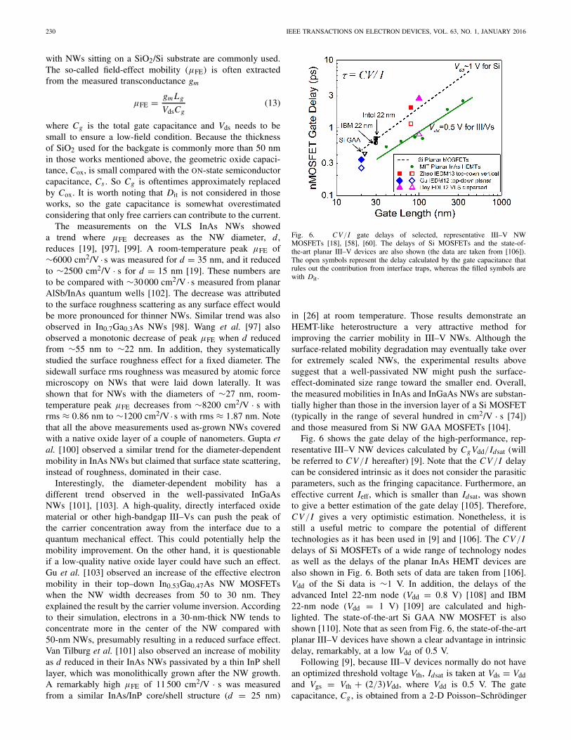
Fig. 6. CV/I gate delays of selected, representative III–V NWMOSFETs [18], [58], [60]. The delays of Si MOSFETs and the state-of-the-art planar III–V devices are also shown (the data are taken from [106]).The open symbols represent the delay calculated by the gate capacitance thatrules out the contribution from interface traps, whereas the filled symbols arewith Dit.
in [26] at room temperature. Those results demonstrate anHEMT-like heterostructure a very attractive method forimproving the carrier mobility in III–V NWs. Although thesurface-related mobility degradation may eventually take overfor extremely scaled NWs, the experimental results abovesuggest that a well-passivated NW might push the surface-effect-dominated size range toward the smaller end. Overall,the measured mobilities in InAs and InGaAs NWs are substan-tially higher than those in the inversion layer of a Si MOSFET(typically in the range of several hundred in cm2/V · s [74])and those measured from Si NW GAA MOSFETs [104].
Fig. 6 shows the gate delay of the high-performance, rep-resentative III–V NW devices calculated by Cg Vdd/Idsat (willbe referred to CV/I hereafter) [9]. Note that the CV/I delaycan be considered intrinsic as it does not consider the parasiticparameters, such as the fringing capacitance. Furthermore, aneffective current Ieff, which is smaller than Idsat, was shownto give a better estimation of the gate delay [105]. Therefore,CV/I gives a very optimistic estimation. Nonetheless, it isstill a useful metric to compare the potential of differenttechnologies as it has been used in [9] and [106]. The CV/Idelays of Si MOSFETs of a wide range of technology nodesas well as the delays of the planar InAs HEMT devices arealso shown in Fig. 6. Both sets of data are taken from [106].Vdd of the Si data is ∼1 V. In addition, the delays of theadvanced Intel 22-nm node (Vdd = 0.8 V) [108] and IBM22-nm node (Vdd = 1 V) [109] are calculated and high-lighted. The state-of-the-art Si GAA NW MOSFET is alsoshown [110]. Note that as seen from Fig. 6, the state-of-the-artplanar III–V devices have shown a clear advantage in intrinsicdelay, remarkably, at a low Vdd of 0.5 V.
Following [9], because III–V devices normally do not havean optimized threshold voltage Vth, Idsat is taken at Vds = Vddand Vgs = Vth + (2/3)Vdd, where Vdd is 0.5 V. The gatecapacitance, Cg , is obtained from a 2-D Poisson–Schrödinger

ZHANG AND LI: III–V NW TRANSISTORS FOR LOW-POWER LOGIC APPLICATIONS: A REVIEW AND OUTLOOK 231
TABLE I
ION COMPARISON BETWEEN III–V AND Si NW DEVICES
coupled simulation of the gate electrostatics at the NW crosssection by Nextnano [107]. Dit, as estimated earlier, is addedto capture the gate voltage stretch-out. Note that two datapoints are shown for each NW device in Fig. 6. The opensymbols represent the delay calculated by the gate capacitancethat rules out the contribution from interface traps, whereas thefilled symbols are with Dit. As we can see, the open symbolsfollow better with the trend of the state-of-the-art planar III–Vdevices (those are HEMT devices that do not have Dit effect)and show advantage over the Si MOSFETs. However, Dit isseen to substantially corrupt the gate delay as it increases thetotal gate capacitance and also degrades current, because asubstantial portion of channel electrons go to interface states,and therefore does not conduct current.
As the CMOS scaling continues, the parasitic and wiringcapacitances have become increasingly significant such thatthe intrinsic gate capacitance is now not dominating. There-fore, it will also be informative to compare ON-state cur-rent at fixed Vdd. Simulation results have shown thatIII–V NW devices (especially InAs) do not outperform Siwhen both operate at their ballistic limit [111]. The reasonis that III–Vs have small electron effective mass leading toreduced density of states and, therefore, reduced gate capac-itance and inversion charge. Nonetheless, the state-of-the-artplanar III–V devices [106], [112] show considerably higherION compared with the advanced Si FinFET technology [113]when ION (at Vdd = 0.5 V and IOFF = 100 nA/μm)is normalized to the actual conducting width. III–V planardevices now operate very close to the ballistic limit [114],while Si devices do not. It is arguable if Si devices caneventually reach the ballistic limit. Those experimental resultsencourage the continuous research on III–V device, includingNWs, for CMOS applications. Table I compares ION of thebest III–V NW MOSFETs to the state-of-the-art Si GAANW device. Currently, for experimental results, III–V NWshave not shown an advantage over Si in terms of drivecurrent. Further enhancement of current would require a sig-nificant improvement of NW/high-k interface quality to bothreduce Dit and increase mobility.
VI. CONCLUSION
In summary, we have reviewed various aspects of the devel-opment of III–V NW transistors. Advantages and challengesof each fabrication approach have been discussed. Althoughthe top–down methods have been prevailing in the industrialmanufacture, the bottom–up methods have been developed to a
point that is worth some seriously considerations for practicaluse, given their potential in the heterogeneous integration andconvenience for in situ passivation through heterostructures.The InAs NWs have been shown to have a very good scalingpotential for beyond-10-nm technology node. Despite so,III–V NW MOSFETs with a sub-10-nm diameter stillremain to be extensively studied by experiment. High oxide–semiconductor interface-trap density, a long-standing historicalproblem for III–Vs, still greatly affects both the OFF-stateand ON-state performance of III–V NW transistors. Surfacepassivation by forming an abrupt heterostructure with someother higher bandgap semiconductors, such InP, is highlightedhere as a very promising technology for both reducing Dit andimproving the carrier transport property.
An NW GAA structure is of interest primarily due to itssuperb gate electrostatics that can allow further gate-lengthscaling. Yet the speed performance could be affected, becausethe NW architecture tends to have an increased ratio betweenthe parasitic capacitance and the useful gate capacitance [104].Note that the parasitic capacitances usually do not scale withthe gate length. New innovations in design and process-ing technologies for maximizing the speed performance ofNW transistors are needed in the future development.
ACKNOWLEDGMENT
X. Li would like to thank Prof. J. del Alamo for hisinsightful comments and critical reading of this paper.
REFERENCES
[1] D. Chattopadhyay, S. K. Sutradhar, and B. R. Nag, “Electron transportin direct-gap III–V ternary alloys,” J. Phys. C, Solid State Phys., vol. 14,no. 6, pp. 891–908, 1981.
[2] T. P. Pearsall and J. P. Hirtz, “The carrier mobilities in Ga0.47In0.53Asgrown by organo-mettalic CVD and liquid-phase epitaxy,” J. CrystalGrowth, vol. 54, no. 1, pp. 127–131, 1981.
[3] J. A. del Alamo, “Nanometre-scale electronics with III–V compoundsemiconductors,” Nature, vol. 479, no. 7373, pp. 317–323, Nov. 2011.
[4] D.-H. Kim, J. A. del Alamo, D. A. Antoniadis, and B. Brar, “Extractionof virtual-source injection velocity in sub-100 nm III–V HFETs,” inIEDM Tech. Dig., 2009, pp. 35.4.1–35.4.4.
[5] T.-W. Kim and J. A. del Alamo, “Injection velocity in thin-channel InAsHEMTs,” in Proc. Compound Semiconductor Week, 23rd Int. Conf.Indium Phosph. Rel. Mater., 2011, pp. 1–4.
[6] D.-H. Kim, J. A. del Alamo, P. Chen, W. Ha, M. Urteaga, and B. Brar,“50-nm E-mode In0.7Ga0.3As PHEMTs on 100-mm InP substrate withfmax > 1 THz,” in IEDM Tech. Dig., 2010, pp. 30.6.1–30.6.4.
[7] E.-Y. Chang, C.-I. Kuo, H.-T. Hsu, C.-Y. Chiang, and Y. Miyamoto,“InAs thin-channel high-electron-mobility transistors with very highcurrent-gain cutoff frequency for emerging submillimeter-wave appli-cations,” Appl. Phys. Exp., vol. 6, no. 3, p. 034001, Mar. 2013.
[8] D.-H. Kim, B. Brar, and J. A. del Alamo, “fT = 688 GHz andfmax = 800 GHz in Lg = 50 nm In0.7Ga0.3As MHEMTs withgm_max > 2.7 mS/μm,” in IEDM Tech. Dig., 2011, pp. 13.6.1–13.6.4.
[9] R. Chau et al., “Benchmarking nanotechnology for high-performance and low-power logic transistor applications,” IEEE Trans.Nanotechnol., vol. 4, no. 2, pp. 153–158, Mar. 2005.
[10] R. Chau, S. Datta, and A. Majumdar, “Opportunities and challenges ofIII–V nanoelectronics for future high-speed, low-power logic applica-tions,” in Proc. IEEE Compound Semiconductor Integr. Circuit Symp.,Oct./Nov. 2005, pp. 17–20.
[11] H. Riel, L.-E. Wernersson, M. Hong, and J. A. del Alamo,“III–V compound semiconductor transistors—From planar to nanowirestructures,” MRS Bull., vol. 39, no. 8, pp. 668–677, 2014.
[12] W. Haensch et al., “Silicon CMOS devices beyond scaling,” IBM J. Res.Develop., vol. 50, nos. 4–5, pp. 339–361, Jul. 2006.

232 IEEE TRANSACTIONS ON ELECTRON DEVICES, VOL. 63, NO. 1, JANUARY 2016
[13] T. N. Theis and P. M. Solomon, “In quest of the ‘next switch’: Prospectsfor greatly reduced power dissipation in a successor to the siliconfield-effect transistor,” Proc. IEEE, vol. 98, no. 12, pp. 2005–2014,Dec. 2010.
[14] I. Ferain, C. A. Colinge, and J.-P. Colinge, “Multigate transistors as thefuture of classical metal–oxide–semiconductor field-effect transistors,”Nature, vol. 479, no. 7373, pp. 310–316, Nov. 2011.
[15] R. S. Wagner and W. C. Ellis, “Vapor-liquid-solid mechanism of singlecrystal growth,” Appl. Phys. Lett., vol. 4, no. 5, p. 89, 1964.
[16] S. A. Fortuna and X. Li, “Metal-catalyzed semiconductor nanowires:A review on the control of growth directions,” Semicond. Sci. Technol.,vol. 25, no. 2, p. 024005, Feb. 2010.
[17] L. E. Fröberg, W. Seifert, and J. Johansson, “Diameter-dependentgrowth rate of InAs nanowires,” Phys. Rev. B, vol. 76, p. 153401,Oct. 2007.
[18] A. W. Dey et al., “High-performance InAs nanowire MOSFETs,” IEEEElectron Device Lett., vol. 33, no. 6, pp. 791–793, Jun. 2012.
[19] A. C. Ford et al., “Diameter-dependent electron mobility of InAsnanowires,” Nano Lett., vol. 9, no. 1, pp. 360–365, 2009.
[20] A. Razavieh et al., “Effect of diameter variation on electrical char-acteristics of Schottky barrier indium arsenide nanowire field-effecttransistors,” ACS Nano, vol. 8, no. 6, pp. 6281–6287, 2014.
[21] E. I. Givargizov, “Fundamental aspects of VLS growth,” J. CrystalGrowth, vol. 31, pp. 20–30, Dec. 1975.
[22] K. Jung, P. K. Mohseni, and X. Li, “Ultrathin InAs nanowire growthby spontaneous Au nanoparticle spreading on indium-rich surfaces,”Nanoscale, vol. 6, no. 24, pp. 15293–15300, 2014.
[23] H. Schmid et al., “Patterned epitaxial vapor-liquid-solid growth ofsilicon nanowires on Si(111) using silane,” J. Appl. Phys., vol. 103,no. 2, p. 024304, 2008.
[24] L. E. Fröberg, C. Rehnstedt, C. Thelander, E. Lind, L.-E. Wernersson,and L. Samuelson, “Heterostructure barriers in wrap gated nanowireFETs,” IEEE Electron Device Lett., vol. 29, no. 9, pp. 981–983,Sep. 2008.
[25] E. Lind, A. I. Persson, L. Samuelson, and L.-E. Wernersson, “Improvedsubthreshold slope in an InAs nanowire heterostructure field-effecttransistor,” Nano Lett., vol. 6, no. 9, pp. 1842–1846, Sep. 2006.
[26] X. Jiang, Q. Xiong, S. Nam, F. Qian, Y. Li, and C. M. Lieber, “InAs/InPradial nanowire heterostructures as high electron mobility devices,”Nano Lett., vol. 7, no. 10, pp. 3214–3218, Oct. 2007.
[27] X. Miao, C. Zhang, and X. Li, “Monolithic barrier-all-around highelectron mobility transistor with planar GaAs nanowire channel,” NanoLett., vol. 13, no. 6, pp. 2548–2552, Jun. 2013.
[28] L. C. Chuang, M. Moewe, C. Chase, N. P. Kobayashi,C. Chang-Hasnain, and S. Crankshaw, “Critical diameter for III–Vnanowires grown on lattice-mismatched substrates,” Appl. Phys. Lett.,vol. 90, no. 4, p. 043115, 2007.
[29] E. P. A. M. Bakkers, M. T. Borgström, and M. A. Verheijen, “Epitaxialgrowth of III–V nanowires on group IV substrates,” MRS Bull., vol. 32,no. 2, pp. 117–122, 2007.
[30] P. Caroff, K. A. Dick, J. Johansson, M. E. Messing, K. Deppert, andL. Samuelson, “Controlled polytypic and twin-plane superlattices inIII–V nanowires,” Nature Nanotechnol., vol. 4, no. 1, pp. 50–55, 2009.
[31] H. J. Joyce et al., “Twin-free uniform epitaxial GaAs nanowires grownby a two-temperature process,” Nano Lett., vol. 7, no. 4, pp. 921–926,2007.
[32] H. J. Joyce, J. Wong-Leung, Q. Gao, H. H. Tan, and C. Jagadish,“Phase perfection in zinc blende and wurtzite III–V nanowires usingbasic growth parameters,” Nano Lett., vol. 10, no. 3, pp. 908–915,2010.
[33] K. A. Dick et al., “Control of III–V nanowire crystal structure bygrowth parameter tuning,” Semicond. Sci. Technol., vol. 25, no. 2,p. 024009, 2010.
[34] Q.-T. Do, K. Blekker, I. Regolin, W. Prost, and F. J. Tegude, “Hightransconductance MISFET with a single InAs nanowire channel,” IEEEElectron Device Lett., vol. 28, no. 8, pp. 682–684, Aug. 2007.
[35] C. Thelander, L. E. Fröberg, C. Rehnstedt, L. Samuelson, andL.-E. Wernersson, “Vertical enhancement-mode InAs nanowire field-effect transistor with 50-nm wrap gate,” IEEE Electron Device Lett.,vol. 29, no. 3, pp. 206–208, Mar. 2008.
[36] M. Egard et al., “Vertical InAs nanowire wrap gate transistors withft > 7 GHz and fmax > 20 GHz,” Nano Lett., vol. 10, no. 3,pp. 809–812, Mar. 2010.
[37] K.-M. Persson et al., “Extrinsic and intrinsic performance of verticalInAs nanowire MOSFETs on Si substrates,” IEEE Trans. ElectronDevices, vol. 60, no. 9, pp. 2761–2767, Sep. 2013.
[38] S. Johansson, E. Memisevic, L.-E. Wernersson, and E. Lind, “High-frequency gate-all-around vertical InAs nanowire MOSFETs on Sisubstrates,” IEEE Electron Device Lett., vol. 35, no. 5, pp. 518–520,May 2014.
[39] J. A. del Alamo, private communication, 2015.[40] C. Thelander et al., “Development of a vertical wrap-gated InAs
FET,” IEEE Trans. Electron Devices, vol. 55, no. 11, pp. 3030–3036,Nov. 2008.
[41] S. A. Fortuna, J. Wen, I. S. Chun, and X. Li, “Planar GaAsnanowires on GaAs (100) substrates: Self-aligned, nearly twin-defectfree, and transfer-printable,” Nano Lett., vol. 8, no. 12, pp. 4421–4427,Dec. 2008.
[42] R. Dowdy, D. A. Walko, S. A. Fortuna, and X. Li, “Realization ofunidirectional planar GaAs nanowires on GaAs (110) substrates,” IEEEElectron Device Lett., vol. 33, no. 4, pp. 522–524, Apr. 2012.
[43] R. S. Dowdy, D. A. Walko, and X. Li, “Relationship betweenplanar GaAs nanowire growth direction and substrate orientation,”Nanotechnology, vol. 24, no. 3, p. 035304, Jan. 2013.
[44] C. Zhang, X. Miao, P. K. Mohseni, W. Choi, and X. Li, “Site-controlledVLS growth of planar nanowires: Yield and mechanism,” Nano Lett.,vol. 14, no. 12, pp. 6836–6841, Dec. 2014.
[45] S. A. Fortuna and X. Li, “GaAs MESFET with a high-mobilityself-assembled planar nanowire channel,” IEEE Electron Device Lett.,vol. 30, no. 6, pp. 593–595, Jun. 2009.
[46] C. Zhang and X. Li, “Planar GaAs nanowire tri-gate MOSFETs byvapor–liquid–solid growth,” Solid-State Electron., vol. 93, pp. 40–42,Mar. 2014.
[47] C. Zhang, R. Dowdy, and X. Li, “High voltage gain MESFET amplifierusing self-aligned MOCVD grown planar GaAs nanowires,” in Proc.Annu. Device Res. Conf. (DRC), Jun. 2013, pp. 63–64.
[48] X. Miao, K. Chabak, C. Zhang, P. K. Mohseni, D. A. Walko, and X. Li,“High-speed planar GaAs nanowire arrays with fmax > 75 GHzby wafer-scale bottom-up growth,” Nano Lett., vol. 15, no. 4,pp. 2780–2786, 2015.
[49] C. Zhang, W. Choi, P. K. Mohseni, and X. Li, “InAs planar nanowiregate-all-around MOSFETs on GaAs substrates by selective lateralepitaxy,” IEEE Electron Device Lett., vol. 36, no. 7, pp. 663–665,Jul. 2015.
[50] J. J. Coleman, R. M. Lammert, M. Osowski, and A. Jones, “Progressin InGaAs-GaAs selective-area MOCVD toward photonic integratedcircuits,” IEEE J. Sel. Topics Quantum Electron., vol. 3, no. 3,pp. 874–884, Jun. 1997.
[51] K. Tomioka, M. Yoshimura, and T. Fukui, “A III–V nanowire channelon silicon for high-performance vertical transistors,” Nature, vol. 488,no. 7410, pp. 189–192, Aug. 2012.
[52] T. Tanaka, K. Tomioka, S. Hara, J. Motohisa, E. Sano, and T. Fukui,“Vertical surrounding gate transistors using single InAs nanowiresgrown on Si substrates,” Appl. Phys. Exp., vol. 3, no. 2, p. 025003,Jan. 2010.
[53] K. Tomioka, M. Yoshimura, E. Nakai, F. Ishizaka, and T. Fukui,“Integration of III-V nanowires on Si: From high-performance ver-tical FET to steep-slope switch,” in IEDM Tech. Dig., Dec. 2013,pp. 4.1.1–4.1.4.
[54] J. Motohisa, J. Noborisaka, J. Takeda, M. Inari, and T. Fukui,“Catalyst-free selective-area MOVPE of semiconductor nanowires on(111)B oriented substrates,” J. Crystal Growth, vol. 272, nos. 1–4,pp. 180–185, Dec. 2004.
[55] K. Tomioka, J. Motohisa, S. Hara, and T. Fukui, “Control of InAsnanowire growth directions on Si,” Nano Lett., vol. 8, no. 10,pp. 3475–3480, Oct. 2008.
[56] Y. Song et al., “III-V junctionless gate-all-around nanowire MOSFETsfor high linearity low power applications,” IEEE Electron Device Lett.,vol. 35, no. 3, pp. 324–326, Mar. 2014.
[57] J. J. Gu, Y. Q. Liu, Y. Q. Wu, R. Colby, R. G. Gordon, andP. D. Ye, “First experimental demonstration of gate-all-around III–VMOSFETs by top-down approach,” in IEDM Tech. Dig., Dec. 2011,pp. 33.2.1–33.2.4.
[58] J. J. Gu et al., “20–80 nm channel length InGaAs gate-all-aroundnanowire MOSFETs with EOT=1.2 nm and lowest SS=63 mV/dec,”in IEDM Tech. Dig., Dec. 2012, pp. 27.6.1–27.6.4.
[59] J. J. Gu et al., “III-V gate-all-around nanowire MOSFET processtechnology: From 3D to 4D,” in IEDM Tech. Dig., Dec. 2012,pp. 23.7.1–23.7.4.
[60] X. Zhao, J. Lin, E. A. Fitzgerald, and J. A. del Alamo, “Verticalnanowire InGaAs MOSFETs fabricated by a top-down approach,” inIEDM Tech. Dig., Dec. 2013, pp. 28.4.1–28.4.4.

ZHANG AND LI: III–V NW TRANSISTORS FOR LOW-POWER LOGIC APPLICATIONS: A REVIEW AND OUTLOOK 233
[61] X. Zhao and J. A. del Alamo, “Nanometer-scale vertical-sidewallreactive ion etching of InGaAs for 3-D III-V MOSFETs,” IEEEElectron Device Lett., vol. 35, no. 5, pp. 521–523, May 2014.
[62] J. Lin, X. Zhao, D. A. Antoniadis, and J. A. del Alamo, “A novel digitaletch technique for deeply scaled III-V MOSFETs,” IEEE ElectronDevice Lett., vol. 35, no. 4, pp. 440–442, Apr. 2014.
[63] S. Lee et al., “Record extrinsic transconductance (2.45 mS/μm atVDS = 0.5 V) InAs/In0.53Ga0.47As channel MOSFETs usingMOCVD source-drain regrowth,” in Proc. Symp. VLSI Technol.,Jun. 2013, pp. T246–T247.
[64] A. Alian, C. Merckling, G. Brammertz, M. Meuris, M. Heyns, andK. D. Meyer, “InGaAs MOS transistors fabricated through a digital-etch gate-recess process and the influence of forming gas anneal ontheir electrical behavior,” ECS J. Solid State Sci. Technol., vol. 1, no. 6,pp. P310–P314, Oct. 2012.
[65] International Technology Roadmap for Semiconductors (ITRS) Report,2013 Edition. [Online]. Available: http://www.itrs.net, accessedJul. 2015.
[66] C. P. Auth and J. D. Plummer, “Scaling theory for cylindrical, fully-depleted, surrounding-gate MOSFET’s,” IEEE Electron Device Lett.,vol. 18, no. 2, pp. 74–76, Feb. 1997.
[67] B. Yu, Y. Yuan, P. M. Asbeck, and Y. Taur, “Scaling ofnanowire transistors,” IEEE Trans. Electron Devices, vol. 55, no. 11,pp. 2846–2858, Nov. 2008.
[68] F. Wang et al., “The scaling of the effective band gaps in indium-arsenide quantum dots and wires,” ACS Nano, vol. 2, no. 9,pp. 1903–1913, 2008.
[69] J. Li and L.-W. Wang, “Band-structure-corrected local density approxi-mation study of semiconductor quantum dots and wires,” Phys. Rev. B,vol. 72, no. 12, p. 125325, Sep. 2005.
[70] E. Lind, M. P. Persson, Y.-M. Niquet, and L.-E. Wernersson,“Band structure effects on the scaling properties of [111] InAsnanowire MOSFETs,” IEEE Trans. Electron Devices, vol. 56, no. 2,pp. 201–205, Feb. 2009.
[71] K. Alam and R. N. Sajjad, “Electronic properties and orientation-dependent performance of InAs nanowire transistors,” IEEE Trans.Electron Devices, vol. 57, no. 11, pp. 2880–2885, Nov. 2010.
[72] C. L. dos Santos and P. Piquini, “Diameter dependence of mechanical,electronic, and structural properties of InAs and InP nanowires: A first-principles study,” Phys. Rev. B, vol. 81, no. 7, p. 075408, Feb. 2010.
[73] Y. Taur, “An analytical solution to a double-gate MOSFET withundoped body,” IEEE Electron Device Lett., vol. 21, no. 5,pp. 245–247, May 2000.
[74] Y. Taur and T. H. Ning, Fundamentals of Modern VLSI Devices.Cambridge, U.K.: Cambridge Univ. Press, 1998.
[75] M. Si et al., “Effects of forming gas anneal on ultrathin InGaAsnanowire metal-oxide-semiconductor field-effect transistors,” Appl.Phys. Lett., vol. 102, no. 9, p. 093505, 2013.
[76] K. Tomioka, M. Yoshimura, and T. Fukui, “Vertical In0.7Ga0.3Asnanowire surrounding-gate transistors with high-k gate dielectric onSi substrate,” in IEDM Tech. Dig., Dec. 2011, pp. 33.3.1–33.3.4.
[77] S. Sasaki et al., “Encapsulated gate-all-around InAs nanowire field-effect transistors,” Appl. Phys. Lett., vol. 103, no. 21, p. 213502, 2013.
[78] T. Bryllert, L.-E. Wernersson, L. E. Fröberg, and L. Samuelson,“Vertical high-mobility wrap-gated InAs nanowire transistor,” IEEEElectron Device Lett., vol. 27, no. 5, pp. 323–325, May 2006.
[79] K.-M. Persson et al., “Vertical InAs nanowire MOSFETs withIDS = 1.34 mA/μm and gm = 1.19 mS/μm at VDS = 0.5 V,” inProc. 70th Annu. Device Res. Conf. (DRC), Jun. 2012, pp. 195–196.
[80] Y. Xuan, H. C. Lin, P. D. Ye, and G. D. Wilk, “Capacitance-voltagestudies on enhancement-mode InGaAs metal-oxide-semiconductorfield-effect transistor using atomic-layer-deposited Al2O3 gatedielectric,” Appl. Phys. Lett., vol. 88, no. 26, p. 263518, 2006.
[81] Y. B. Kim, M. S. Kang, D. K. Choi, T. Lee, and J. Ahn, “Physicaland electrical properties of atomic layer deposited HfO2 for gatedielectric application,” J. Korean Phys. Soc., vol. 42, pp. S1146–S1148,Apr. 2003.
[82] Y. Xuan, Y. Q. Wu, H. C. Lin, T. Shen, and P. D. Ye, “Submicrometerinversion-type enhancement-mode InGaAs MOSFET with atomic-layer-deposited Al2O3 as gate dielectric,” IEEE Electron Device Lett.,vol. 28, no. 11, pp. 935–938, Nov. 2007.
[83] Y. Xuan, T. Shen, M. Xu, Y. Q. Wu, and P. D. Ye, “High-performancesurface channel In-rich In0.75Ga0.25As MOSFETs with ALD high-kas gate dielectric,” in IEDM Tech. Dig., Dec. 2008, pp. 1–4.
[84] P. D. Ye, “Main determinants for III–V metal-oxide-semiconductorfield-effect transistors (invited),” J. Vac. Sci. Technol. A, vol. 26, no. 4,p. 697, 2008.
[85] J. J. Gu, A. T. Neal, and P. D. Ye, “Effects of (NH4)2S passivationon the off-state performance of 3-dimensional InGaAs metal-oxide-semiconductor field-effect transistors,” Appl. Phys. Lett., vol. 99, no. 15,p. 152113, 2011.
[86] M. Radosavljevic et al., “Non-planar, multi-gate InGaAs quantum wellfield effect transistors with high-K gate dielectric and ultra-scaled gate-to-drain/gate-to-source separation for low power logic applications,” inIEDM Tech. Dig., Dec. 2010, pp. 6.1.1–6.1.4.
[87] C. W. Wilmsen, “The MOS/InP interface,” Critical Rev. Solid StateSci., vol. 5, no. 3, pp. 313–317, Oct. 1975.
[88] D. L. Lile and D. A. Collins, “An InP MIS diode,” Appl. Phys. Lett.,vol. 28, no. 9, p. 554, 1976.
[89] S. Kundu, N. N. Halder, D. Biswas, P. Banerji, T. Shripathi, andS. Chakraborty, “Role of ultra thin pseudomorphic InP layer toimprove the high-k dielectric/GaAs interface in realizing metal-oxide-semiconductor capacitor,” J. Appl. Phys., vol. 112, no. 3, p. 034514,2012.
[90] M. Xu et al., “New insight into Fermi-level unpinning on GaAs: Impactof different surface orientations,” in IEDM Tech. Dig., Dec. 2009,pp. 1–4.
[91] D.-G. Park, Z. Chen, A. E. Botchkarev, S. N. Mohammad, andH. Morkoç, “Interface properties of Si3N4/Si/n-GaAs metal-insulator-semiconductor structure using a Si interlayer,” Philos. Mag. B, vol. 74,no. 3, pp. 219–234, Sep. 2006.
[92] S. Tiwari, S. L. Wright, and J. Batey, “Unpinned GaAs MOS capacitorsand transistors,” IEEE Electron Device Lett., vol. 9, no. 9, pp. 490–499,Sep. 1988.
[93] D.-G. Park, D. M. Diatezua, Z. Chen, S. N. Mohammad, andH. Morkoç, “Characteristics of Si3N4/Si/n-GaAs metal-insulator-semiconductor interfaces grown on GaAs(111)B substrate,” Appl. Phys.Lett., vol. 69, no. 20, p. 3025, 1996.
[94] Z. Wang, D. S. L. Mui, A. L. Demirel, D. Biswas, J. Reed, andH. Morkoç, “Gate quality Si3N4/Si/n-In0.53Ga0.47As metal-insulator-semiconductor capacitors,” Appl. Phys. Lett., vol. 61, no. 15, p. 1826,1992.
[95] C. L. Hinkle et al., “Detection of Ga suboxides and their impact onIII–V passivation and Fermi-level pinning,” Appl. Phys. Lett., vol. 94,no. 16, p. 162101, 2009.
[96] M. Lundstrom, “Elementary scattering theory of the Si MOSFET,”IEEE Electron Device Lett., vol. 18, no. 7, pp. 361–363, Jul. 1997.
[97] F. Wang et al., “Surface roughness induced electron mobilitydegradation in InAs nanowires,” Nanotechnology, vol. 24, no. 37,p. 375202, Sep. 2013.
[98] J. J. Hou et al., “Diameter dependence of electron mobility in InGaAsnanowires,” Appl. Phys. Lett., vol. 102, no. 9, p. 093112, 2013.
[99] M. Scheffler, S. Nadj-Perge, L. P. Kouwenhoven, M. T. Borgström,and E. P. A. M. Bakkers, “Diameter-dependent conductance of InAsnanowires,” J. Appl. Phys., vol. 106, no. 12, p. 124303, 2009.
[100] N. Gupta et al., “Temperature-dependent electron mobility in InAsnanowires,” Nanotechnology, vol. 24, no. 22, p. 225202, Jun. 2013.
[101] J. W. W. van Tilburg, R. E. Algra, W. G. G. Immink, M. Verheijen,E. P. A. M. Bakkers, and L. P. Kouwenhoven, “Surface passivatedInAs/InP core/shell nanowires,” Semicond. Sci. Technol., vol. 25, no. 2,p. 024011, Feb. 2010.
[102] C. R. Bolognesi, H. Kroemer, and J. H. English, “Well widthdependence of electron transport in molecular-beam epitaxially grownInAs/AlSb quantum wells,” J. Vac. Sci. Technol. B, vol. 10, no. 2,pp. 877–879, 1992.
[103] J. J. Gu, H. Wu, Y. Liu, A. T. Neal, R. G. Gordon, and P. D. Ye,“Size-dependent-transport study of In0.53Ga0.47As gate-all-aroundnanowire MOSFETs: Impact of quantum confinement and volumeinversion,” IEEE Electron Device Lett., vol. 33, no. 7, pp. 967–969,Jul. 2012.
[104] S. D. Suk et al., “Investigation of nanowire size dependency onTSNWFET,” in IEDM Tech. Dig., Dec. 2007, pp. 891–894.
[105] M.-H. Na, E. J. Nowak, W. Haensch, and J. Cai, “The effectivedrive current in CMOS inverters,” in IEDM Tech. Dig., Dec. 2002,pp. 121–124.
[106] D.-H. Kim and J. A. del Alamo, “Scalability of sub-100 nm InAsHEMTs on InP substrate for future logic applications,” IEEE Trans.Electron Devices, vol. 57, no. 7, pp. 1504–1511, Jul. 2010.
[107] S. Birner et al., “nextnano: General purpose 3-D simulations,” IEEETrans. Electron Devices, vol. 54, no. 9, pp. 2137–2142, Sep. 2007.
[108] C. Auth et al., “A 22 nm high performance and low-power CMOStechnology featuring fully-depleted tri-gate transistors, self-alignedcontacts and high density MIM capacitors,” in Tech. Dig. Symp. VLSITechnol., Jun. 2012, pp. 131–132.

234 IEEE TRANSACTIONS ON ELECTRON DEVICES, VOL. 63, NO. 1, JANUARY 2016
[109] S. Narasimha et al., “22 nm high-performance SOI technologyfeaturing dual-embedded stressors, epi-plate high-K deep-trenchembedded DRAM and self-aligned via 15 LM BEOL,” in IEDM Tech.Dig., Dec. 2012, pp. 3.3.1–3.3.4.
[110] S. Bangsaruntip et al., “Density scaling with gate-all-around siliconnanowire MOSFETs for the 10 nm node and beyond,” in IEDM Tech.Dig., Dec. 2013, pp. 20.2.1–20.2.4.
[111] R. Kim, U. E. Avci, and I. A. Young, “Source/drain doping effects andperformance analysis of ballistic III–V n-MOSFETs,” IEEE J. ElectronDevices Soc., vol. 3, no. 1, pp. 37–43, Jan. 2015.
[112] S. Lee et al., “Record Ion (0.50 mA/μm at VDD = 0.5 Vand Io f f = 100 nA/μm) 25 nm-gate-length ZrO2/InAs/InAlAsMOSFETs,” in Symp. VLSI Technol. Dig. Tech. Papers, Jun. 2014,pp. 1–2.
[113] S. Natarajan et al., “A 14 nm logic technology featuring 2nd-generationFinFET, air-gapped interconnects, self-aligned double patterning anda 0.0588 μm2 SRAM cell size,” in Proc. IEEE IEDM, Dec. 2014,pp. 3.7.1–3.7.3.
[114] N. Kharche, G. Klimeck, D.-H. Kim, J. A. del Alamo, andM. Luisier, “Multiscale metrology and optimization of ultra-scaledInAs quantum well FETs,” IEEE Trans. Electron Devices, vol. 58,no. 7, pp. 1963–1971, Jul. 2011.
Chen Zhang received the B.S. and M.S. degreesin electronic engineering from Tsinghua University,Beijing, China, in 2007 and 2010, respectively, andthe Ph.D. degree in electrical and computer engi-neering from the University of Illinois at Urbana-Champaign, Urbana, IL, USA, in 2015.
He is currently with IBM Research, Albany,NY, USA. His thesis research involves the growthand fabrication of III–V nanowire transistors andMOSFET device physics.
Xiuling Li received the B.S. degree from PekingUniversity, Beijing, China, and the Ph.D. degreefrom the University of California at Los Angeles,Los Angeles, CA, USA.
She joined the University of Illinois at Urbana-Champaign, Urbana, IL, USA, in 2007, and iscurrently a Professor with the Department ofElectrical and Computer Engineering. Her currentresearch interests include nanostructured semicon-ductor materials and devices.