ieee transactions on computers, vol. 58,...
TRANSCRIPT

A Flexible Software-Based Framework forOnline Detection of Hardware Defects
Kypros Constantinides, Student Member, IEEE, Onur Mutlu, Member, IEEE,
Todd Austin, Member, IEEE, and Valeria Bertacco, Member, IEEE
Abstract—This work proposes a new, software-based, defect detection and diagnosis technique. We introduce a novel set of
instructions, called Access-Control Extensions (ACE), that can access and control the microprocessor’s internal state. Special
firmware periodically suspends microprocessor execution and uses the ACE instructions to run directed tests on the hardware. When a
hardware defect is present, these tests can diagnose and locate it, and then activate system repair through resource reconfiguration.
The software nature of our framework makes it flexible: testing techniques can be modified/upgraded in the field to trade-off
performance with reliability without requiring any change to the hardware. We describe and evaluate different execution models for
using the ACE framework. We also describe how the proposed ACE framework can be extended and utilized to improve the quality of
post-silicon debugging and manufacturing testing of modern processors. We evaluated our technique on a commercial chip-
multiprocessor based on Sun’s Niagara and found that it can provide very high coverage, with 99.22 percent of all silicon defects
detected. Moreover, our results show that the average performance overhead of software-based testing is only 5.5 percent. Based on
a detailed register transfer level (RTL) implementation of our technique, we find its area and power consumption overheads to be
modest, with a 5.8 percent increase in total chip area and a 4 percent increase in the chip’s overall power consumption.
Index Terms—Reliability, hardware defects, online defect detection, testing, online self-test, post-silicon debugging, manufacturing
test.
Ç
1 INTRODUCTION
THE impressive growth of the semiconductor industryover the last few decades is fueled by continuous silicon
scaling, which offers smaller, faster, and cheaper transistorswith each new technology generation. However, challengesin producing reliable components in these extremely densetechnologies are growing, with many device expertswarning that continued scaling will inevitably lead tofuture generations of silicon technology being much lessreliable than present ones [4], [53]. Processors manufac-tured in future technologies will likely experience failuresin the field due to silicon defects occurring during systemoperation. In the absence of any viable alternative technol-ogy, the success of the semiconductor industry in the futurewill depend on the creation of cost-effective mechanisms totolerate silicon defects in the field (i.e., during operation).
The challenge—tolerating hardware defects. To toleratepermanent hardware faults (i.e., silicon defects) encounteredduring operation, a reliable system requires the inclusion ofthree critical capabilities: 1) mechanisms for detection anddiagnosis of defects, 2) recovery techniques to restore correctsystem state after a fault is detected, and 3) repair mechan-isms to restore correct system functionality for futurecomputation. Fortunately, research in chip-multiprocessor(CMP) architectures already provides for the latter two
requirements. Researchers have pursued the developmentof global checkpoint and recovery mechanisms; examples ofthese include SafetyNet [52] and ReVive [42], [39]. Theselow-cost checkpointing mechanisms provide the capabilitiesnecessary to implement system recovery. Additionally, thehighly redundant nature of future CMPs will allow low-costrepair through the disabling of defective processing ele-ments [48]. With a sufficient number of processing re-sources, the performance of a future parallel system willgracefully degrade as manifested defects increase.
Given the existence of low-cost mechanisms for systemrecovery and repair, the remaining major challenge in thedesign of a defect-tolerant CMP is the development of low-cost defect detection techniques. Existing online hardware-based defect detection and diagnosis techniques can beclassified into two broad categories: 1) continuous: those thatcontinuously check for execution errors and 2) periodic:those that periodically check the processor’s logic.
Existing defect tolerance techniques and their short-comings. Examples of continuous techniques are DualModular Redundancy (DMR) [51], lockstep systems [27],and DIVA [2]. These techniques detect silicon defects byvalidating the execution through independent redundantcomputation. However, independent redundant computa-tion requires significant hardware cost in terms of siliconarea (100 percent extra hardware in the case of DMR andlockstep systems). Furthermore, continuous checking con-sumes significant energy and requires part of the powerenvelope to be dedicated to it. In contrast, periodictechniques check periodically the integrity of the hardwarewithout requiring redundant execution [50]. These techni-ques rely on checkpointing and recovery mechanisms thatprovide computational epochs and a substrate for spec-ulative unchecked execution. At the end of each computa-tional epoch, the hardware is checked by on-chip testers. If
IEEE TRANSACTIONS ON COMPUTERS, VOL. 58, NO. 8, AUGUST 2009 1063
. K. Constantinides, T. Austin, and V. Bertacco, are with the University ofMichigan, Ann Arbor, 2260 Hayward, 2773 CSE, MI 48109.E-mail: {kypros, austin, valeria}@umich.edu.
. O. Mutlu is with the Carnegie Mellon University, 5000 Forbes Avenue,ECE-HH-A305, Pittsburgh, PA 15213. E-mail: [email protected].
Manuscript received 18 Feb 2008; revised 30 Aug. 2008; accepted 20 Nov.2008; published online 20 Mar. 2009.Recommended for acceptance by C. Bolchini.For information on obtaining reprints of this article, please send e-mail to:[email protected], and reference IEEECS Log Number TC-2008-02-0078.Digital Object Identifier no. 10.1109/TC.2009.52.
0018-9340/09/$25.00 � 2009 IEEE Published by the IEEE Computer Society
Authorized licensed use limited to: University of Michigan Library. Downloaded on May 11,2010 at 14:36:06 UTC from IEEE Xplore. Restrictions apply.

the hardware tests succeed, the results produced during theepoch are committed and execution proceeds to the nextcomputational epoch. Otherwise, the system is deemeddefective and system repair and recovery are required.
The on-chip testers employed by periodic defect tolerancetechniques rely on the same Built-In-Self-Test (BIST) techni-ques that are used predominantly during manufacturing test[7]. BIST techniques use specialized circuitry to generate testpatterns and validate the responses generated by thehardware. There are two main ways to generate test patternson chip: 1) by using pseudorandom test pattern generatorsand 2) by storing on-chip previously generated test vectorsthat are based on a specific fault model. Unfortunately, bothof these approaches have significant drawbacks. The firstapproach does not follow any specific testing strategy(targeted fault model), and therefore, requires extendedtesting times to achieve good fault coverage [7]. The secondapproach not only requires significant hardware overhead[10] to store the test patterns on chip but also binds a specifictesting approach (i.e., fault model) into silicon. On the otherhand, as the nature of wearout-related silicon defects and thetechniques to detect them are under continuous exploration[17], binding specific testing approaches into silicon might bepremature, and therefore, undesirable.
As of today, hardware-based defect tolerance techniqueshave one or both of the following two major disadvantages:
1. Cost: They require significant additional hardware toimplement a specific testing strategy.
2. Inflexibility: They bind specific test patterns and aspecific testing approach (e.g., based on a specificfault model) into silicon. Thus, it is impossible tochange the testing strategy and test patterns after theprocessor is deployed in the field. Flexible defecttolerance solutions that can be upgraded in the fieldare very desirable.
High-level overview of our approach. Our goal in thiswork is to develop a low-cost, flexible defect tolerancetechnique that can be modified and upgraded in the field. Tothis end, we propose to implement hardware defectdetection and diagnosis in software. In our approach, thehardware provides the necessary substrate to facilitatetesting and the software makes use of this substrate toperform the testing. We introduce specialized Access-Control Extension (ACE) instructions that are capable ofaccessing and controlling virtually any portion of themicroprocessor’s internal state. Special firmware periodi-cally suspends microprocessor execution and uses the ACEinstructions to run directed tests on the hardware and detectif any component has become defective.
Fig. 1 shows how the ACE framework fits in thehardware/software stack below the operating system layer.
Our approach provides particularly wide coverage, as it notonly tests the internal processor control and instructionsequencing mechanisms through software functional testing,but it can also check all datapaths, routers, interconnect, andmicroarchitectural components by issuing ACE instructiontest sequences.
2 WHY DOES SILICON FAIL? A BRIEF OVERVIEW
OF SILICON FAILURE MECHANISMS
We first provide a brief overview of the silicon failuremechanisms that motivate the solution we propose in thiswork. The interested reader can refer to [14], [44], [49], [54],[23] for a detailed treatment of these mechanisms.
Time-dependent wearout:
. Electromigration: Due to the momentum transferbetween the current-carrying electrons and the hostmetal lattice, ions in a conductor can move in thedirection of the electron current. This ion movementis called electromigration [14]. Gradually, this ionmovement can cause clustered vacancies that cangrow into voids. These voids can eventually growuntil they block the current flow in the conductor.This leads to increased resistance and propagationdelay, which, in turn, leads to possible device failure.Other effects of electromigration are fractures andshorts in the interconnect. The trend of increasingcurrent densities in future technologies increases theseverity of electromigration, leading to a higherprobability of observing open and short-circuitnodes over time [18].
. Gate Oxide Wearout: Thin gate oxides lead toadditional failure modes as devices become subjectto gate oxide wearout (or Time-Dependent Di-electric Breakdown, TDDB) [14]. Over time, gateoxides can break down and become conductive. Ifenough material in the gate breaks down, aconduction path can form from the transistor gateto the substrate, essentially shorting the transistorand rendering it useless [18], [23]. Fast clocks, hightemperatures, and voltage scaling limitations arewell-established architectural trends that aggravatethis failure mode [54].
. Hot Carrier Degradation (HCD): As carriers movealong the channel of an MOSFET and experienceimpact ionization near the drain end of the device, itis possible that they gain sufficient kinetic energy tobe injected into the gate oxide [14]. This phenomen-on is called Hot Carrier Injection. Hot carriers candegrade the gate dielectric, causing shifts in thresh-old voltage and eventually device failure. HCD ispredicted to worsen for future thinner oxide andshorter channel lengths [23].
Transistor infant mortality. Extreme device scaling alsoexacerbates early transistor failures. Early transistor failuresare caused by weak transistors that escape postmanufactur-ing validation tests. These weak transistors work initially,but they have dimensional and doping deficiencies thatsubject them to much higher stress than robust transistors.Quickly (within days to months), they will break downfrom stress and render the device unusable. Traditionally,early transistor failures have been reduced throughaggressive burn-in testing, where, before being placed inthe field, devices are subjected to high voltage andtemperature testing to accelerate the failure of weak
1064 IEEE TRANSACTIONS ON COMPUTERS, VOL. 58, NO. 8, AUGUST 2009
Fig. 1. The ACE framework fits in the hardware/software stack below the
operating system.
Authorized licensed use limited to: University of Michigan Library. Downloaded on May 11,2010 at 14:36:06 UTC from IEEE Xplore. Restrictions apply.

transistors [7]. Those that survive the burn-in testing arelikely to be robust devices, thereby ensuring a long productlifetime. However, in the deep-submicron regime, burn-inbecomes less effective as devices are subject to thermalrunaway effects, where increased temperature leads toincreased leakage current, which, in turn, leads to evenhigher temperatures [37]. The end result is that aggressiveburn-in of deep-submicron silicon can destroy even robustdevices. Manufacturers are forced to either sacrifice yieldby deploying aggressive burn-in testing or experience morefrequent early failures in the field by using less aggressiveburn-in testing.
Manufacturing defects that escape testing. Opticalproximity effects, airborne impurities, and processingmaterial defects can all lead to the manufacturing of faultytransistors and interconnect [44]. Moreover, deep-submicrongate oxides have become so thin that manufacturingvariation can lead to currents penetrating the gate, renderingit unusable [49]. Even small amounts of manufacturingvariation in the gate oxide could render the device unusable.The problem of manufacturing defects is compounded bythe immense complexity of current designs. Design com-plexity makes it more difficult to test for defects duringmanufacturing. Vendors are forced to either spend moretime with parts on the tester, which reduces profits byincreasing time-to-market, or risk the possibility of untesteddefects escaping to the field. Moreover, in highly complexdesigns, many defects are not testable without additionalhardware support. As a result, even in today’s manufactur-ing environment, untestable defects can escape testing andmanifest themselves later on in the field.
Our goal. To overcome the possible errors caused by theaforementioned silicon failure mechanisms, our goal in thiswork is to develop a flexible, low-cost silicon defect detectionand diagnosis technique. We next describe our technique indetail.
3 SOFTWARE-BASED DEFECT DETECTION
AND DIAGNOSIS
A key challenge in implementing a software-based defectdetection and diagnosis technique is the development ofeffective software routines to check the underlying hard-ware. Commonly, software routines for this task sufferfrom the inherent inability of the software layer to observeand control the underlying hardware, resulting in eitherexcessively long test sequences or poor defect coverage.Current microprocessor designs allow only minimal accessto their internal state by the software layer; often all thatsoftware can access consists of the register file and a fewcontrol registers (such as the program counter (PC), statusregisters, etc.). Although this separation provides protec-tion from malicious software, it also largely limits thedegree to which stock hardware can utilize software to testfor silicon defects.
To overcome this limited accessibility, we proposearchitectural support through an extension to the proces-sor’s ISA. Our extension adds a set of special instructionsenabling full observability and control of the hardware’sinternal state. These ACE instructions are capable of read-ing/writing from/to any part of the microprocessor’sinternal state. ACE instructions make it possible to probeunderlying hardware and systematically and efficientlyassess if any hardware component is defective.
3.1 An ACE-Enhanced Architecture
A microprocessor’s state can be partitioned into two parts:accessible from the software layer (e.g., register file, PC,etc.) or not accessible (e.g., reorder buffer, load/storequeues, etc.). An ACE-enhanced microarchitecture allowsthe software layer to access and control (almost) all of themicroprocessor’s state. This is done by using ACE instruc-tions that copy a value from an architectural register to anyother part of the microprocessor’s state and vice versa.
This approach inherently requires the architecture toaccess the underlying microarchitectural state. To providethis accessibility without a large hardware overhead, weleverage the existing scan chain infrastructure. Most modernprocessor designs employ full hold-scan techniques to aidand automate the manufacturing testing process [30], [62].Fig. 2 shows a typical scan flip-flop design [38], [30]. Thesystem flip-flop is used during the normal operating mode,while the scan portion is used during testing to load thesystem with test patterns and to read out the test responses.Our approach extends the existing scan chain using ahierarchical, tree-structured organization to provide fastsoftware access to different microarchitectural components.
ACE domains and segments. In our ACE extensionimplementation, the microprocessor design is logicallypartitioned into several ACE domains. An ACE domainconsists of the state elements and combinational logicassociated with a specific part of the microprocessor. EachACE domain is further subdivided into ACE segments asshown in Fig. 3a. Each ACE segment includes only a fixednumber of storage bits, which is the same as the width of anarchitectural register (64 bits in our design).
ACE instructions. Using this hierarchical structure, ACEinstructions can read or write any part of the micropro-cessor’s state. Table 1 shows a description of the ACEinstruction set extensions.
CONSTANTINIDES ET AL.: A FLEXIBLE SOFTWARE-BASED FRAMEWORK FOR ONLINE DETECTION OF HARDWARE DEFECTS 1065
Fig. 2. A typical scan flip-flop (adapted from [38]).
Fig. 3. The ACE Architecture: (a) the chip is logically partitioned intomultiple ACE domains. Each ACE domain includes several ACEsegments. The union of all ACE segments comprises the full chip’sstate (excluding SRAM structures). (b) Data are transferred from/to theregister file to/from an ACE segment through the bidirectional ACE tree.
Authorized licensed use limited to: University of Michigan Library. Downloaded on May 11,2010 at 14:36:06 UTC from IEEE Xplore. Restrictions apply.

ACE_set copies a value from an architectural register tothe scan state (scan portion in Fig. 2) of the specified ACEsegment at-speed (i.e., at the processor’s clock frequency).Similarly, ACE_get loads a value from the scan state of thespecified ACE segment to an architectural register at-speed.These two instructions can be used for manipulating thescan state through software-accessible architectural state.The ACE_swap instruction is used for swapping the scanstate with the processor state (system flip-flops) of the ACEsegment by asserting both the UPDATE and the CAPTUREsignals (see Fig. 2).
Finally, ACE_test is a test-specific instruction thatperforms a three-cycle atomic operation for orchestratingthe actual testing of the underlying hardware (see Section 3.2for example).
In order to avoid any malicious use of the ACEinfrastructure, ACE instructions are privileged instructionsthat can be used only by ACE firmware. ACE firmwareroutines are special applications running between theoperating system layer and the hardware in a trustedmode, similarly to other firmware, such as device drivers.
ACE tree. During the execution of an ACE instruction,data need to be transferred from the register file to any partof the chip that contains microarchitectural state. In order toavoid long interconnect, which would require extrarepeaters and buffering circuitry, the data transfer betweenthe register file and the ACE segments is pipelined throughthe ACE tree as shown in Fig. 3b. At the root of the ACE treeis the register file while the ACE segments are its leaves. Ateach intermediate tree level, there is an ACE node that isresponsible for buffering and routing the data based on theexecuted operation. The ACE tree is a bidirectional treeallowing data transfers from the register file to the ACEsegments and back.
Design complexity. We believe that since the ACE Tree isa regular structure that routes data from the register file tothe scan chains and vice versa, its implementation andinsertion into the microprocessor implementation can beautomated by CAD tools, similar to the way that scan chainsare automatically implemented and inserted in currentmicroprocessors today. The main intrusive portion of theACE Tree that needs interaction with existing processorcomponents are the additional read/write ports needed toconnect the root of the ACE Tree to the processor register file.Similarly, the ACE instruction set extensions are likely notintrusive to the microarchitecture since their operations arerelatively simple and their implementation does not affectthe implementation of other instructions in the ISA.
3.2 ACE-Based Online Testing
ACE instruction set extensions make it possible to craftprograms that can efficiently and accurately detect theunderlying hardware defects. The approach taken inbuilding test programs, however, must have high coverage,even in the presence of defects that might affect thecorrectness of ACE instruction execution and test programs.This section describes how test programs are designed.
ACE testing and diagnosis. Special firmware periodi-cally suspends normal processor execution and uses theACE infrastructure to perform high-quality testing of theunderlying hardware. A test program exercises the under-lying hardware with previously generated test patterns andvalidates the test responses. Both the test patterns and theassociated test responses are stored in physical memory.The pseudocode of a firmware code segment that applies atest pattern and validates the test response is shown inFig. 4. First, the test program stops normal execution anduses the ACE_set instruction to load the scan state with atest pattern (Step 1). Once the test pattern is loaded into thescan state, a three-cycle atomic ACE_test instruction isexecuted (Step 2). In the first cycle, the processor state isloaded with the test pattern by swapping the processor statewith the scan state. The next cycle is the actual test cycle,where the combinational logic generates the test response.In the third cycle, by swapping again the processor statewith the scan state, the processor state is restored while thetest response is copied to the scan state for furthervalidation. The final phase (Step 3) of the test routine usesthe ACE_get instruction to read and validate the testresponse from the scan state. If a test pattern fails toproduce the correct response at the end of Step 3, the testprogram indicates which part of the hardware is defective1
and disables it through system reconfiguration [48], [13].Given this software-based testing approach, the firm-
ware designer can easily change the level of defect coverageby varying the number of test patterns. As a test programexecutes more patterns, coverage increases. We use auto-matic test pattern generation (ATPG) tools [7] to generatecompact test pattern sets adhering to specific fault models.
Basic core functional testing. When performing ACEtesting, there is one initial challenge to overcome: ACEtesting firmware relies on the correctness of a set of basic corefunctionalities that loads test patterns, executes ACEinstructions, and validates the test response. If the core hasa defect that prevents the correct execution of the ACEfirmware, then ACE testing cannot be performed reliably. Tobypass this problem, we craft specific programs to test thebasic functionalities of a core before running any ACE testingfirmware. If these programs do not report success in a timelymanner to an independent auditor (e.g., the operatingsystem running on the other cores), then we assume thatan irrecoverable defect has occurred on the core and wepermanently disable it. If the basic core functionalities arefound to be intact, finer grained ACE testing can begin.
1066 IEEE TRANSACTIONS ON COMPUTERS, VOL. 58, NO. 8, AUGUST 2009
TABLE 1The ACE Instruction Set Extensions
1. By interpreting the correspondence between erroneous response bitsand ACE domains.
Fig. 4. ACE firmware: Pseudocode for 1) loading a test pattern,
2) testing, and 3) validating the test response.
Authorized licensed use limited to: University of Michigan Library. Downloaded on May 11,2010 at 14:36:06 UTC from IEEE Xplore. Restrictions apply.

3.3 ACE Testing in a Checkpointingand Recovery Environment
We incorporate the ACE testing framework within amultiprocessor checkpointing and recovery mechanism(e.g., SafetyNet [52] or ReVive [42]) to provide support forsystem-level recovery. When a defect is detected, the systemstate is recovered to the last checkpoint (i.e., correct state)after the system is repaired.
In a checkpoint/recovery system, the release of acheckpoint is an irreversible action. Therefore, the systemmust execute the ACE testing firmware at the end of eachcheckpoint interval to test the integrity of the whole chip. Acheckpoint is released only if ACE testing finds no defects.With this policy, the performance overhead induced byrunning the ACE testing firmware depends directly on thelength of the checkpoint interval, that is, longer intervalslead to lower performance overhead. We explore the trade-off between checkpoint interval size and ACE testingperformance overhead in Section 5.4.
3.4 Algorithmic Flow of ACE-Based Online Testing
Table 2 shows the flow of ACE-Based Online testing in acheckpointing and recovery environment with single-threaded execution. Other execution models are examinedin the next section. Two points are worth noting in thealgorithm. First, a lightweight context switch is performedfrom the application thread to the ACE testing thread at thebeginning of the test and vice versa at the end of the test.Lightweight context switching [1], [28] in a single cycle issupported by many simultaneously multithreaded proces-sors today, including Sun’s UltraSPARC T1. If lightweightcontext switch support is not available, then a pipelineflush is required. Our results show that context switchpenalty, even if it is hundreds of cycles, only negligiblyincreases the overhead of ACE testing. Second, if the basiccore functional test fails, the core is disabled and executiontraps to the system software. If the ACE firmware test fails,the system software performs defect diagnosis to localizethe defect. To do so, the system software maps the ACEsegments that fail to match the expected test response tospecific hardware components (i.e., the combinational logicdriving the flip-flops of the ACE segments). If reconfigur-ability support is provided within those hardware compo-nents, the ACE firmware can pinpoint these components to
be disabled. Since our focus is on flexible defect detection,we leave fault analysis and recovery to future work.
3.5 ACE Testing Execution Models
Single-threaded sequential ACE testing. The simplestexecution model for ACE testing is to implement the ACEtesting process at the end of each checkpoint interval. In thisexecution model, the application runs normally on theprocessor until the buffering resources dedicated to thecheckpoint are full and a new checkpoint needs to be taken.At this point, a context switch between the applicationprocess and the ACE testing process happens. If the ACEtesting routine deems the underlying hardware defect free,a new checkpoint of the processor state is taken and theexecution of the application process is resumed. Otherwise,system repair and recovery are triggered. Fig. 5a illustratesthis single-threaded sequential execution model.
SMT-based ACE testing. In processors that supportsimultaneous multithreading (SMT) execution [47], [21],[59], it is possible for the ACE firmware to run simulta-neously with the application threads running on separateexecution contexts. This execution model is illustrated inFig. 5b and could be higher performance since it overlaps thelatency of ACE testing with actual application execution.
Fortunately, the majority of the instructions used by theACE testing firmware do not entail any synchronizationrequirements between the ACE testing thread and the otherthreads running on the processor. For example, the ACEinstructions used to load a test pattern into the scan state(ACE_set) or read and validate a test response (ACE_get)do not affect the execution of other threads running on theprocessor. The work performed by these instructions can befully overlapped with application execution.
However, the ACE_test instruction momentarilychanges the microarchitectural state of the entire processor,and thus, affects the normal execution of all running threads.To avoid the incorrect execution of other running threadswhen an ACE_test instruction is executed by the ACEtesting thread, all other threads need to pause execution.This is implemented by using simple synchronizationhardware that pauses execution of all other threads (i.e.,stalls their pipelines) when an ACE_test instruction startsexecution and resumes their execution once the test instruc-tion is completed. Note that during testing, the processor’smicroarchitectural state is stored in the scan state. Themicroarchitectural state gets restored right after the test cycle(see Section 3.1) enabling the seamless resumption of normalprocessor execution.
The advantage of the SMT-based ACE testing model isits lower performance overhead compared to single-threaded sequential ACE testing. The disadvantage is thatthis model requires a separate SMT context to be present in
CONSTANTINIDES ET AL.: A FLEXIBLE SOFTWARE-BASED FRAMEWORK FOR ONLINE DETECTION OF HARDWARE DEFECTS 1067
TABLE 2Algorithmic Flow of ACE-Based Testingin a Checkpoint/Recovery Environment
Fig. 5. Different execution models of ACE testing: (a) Illustrates ACEtesting in a single-threaded sequential execution model, where the ACEtesting thread is run exclusively after application execution. (b) The ACEtesting thread runs simultaneously with the application in a 2-way SMTexecution environment. (c) ACE testing is interleaved with applicationexecution and run in the shadow of L2 cache misses.
Authorized licensed use limited to: University of Michigan Library. Downloaded on May 11,2010 at 14:36:06 UTC from IEEE Xplore. Restrictions apply.

the underlying processor. Note that to guarantee correctrecovery, with this execution model, the recovery mechan-ism needs to buffer the last two checkpoints.
Interleaved ACE testing in the shadow of L2 misses.When the ACE testing thread is sharing the processorresources with other critical applications, it is important toavoid penalizing the performance of these critical applica-tions due to hardware testing. Performance penalties can bereduced by allowing the ACE testing thread to execute onlywhen the processor resources are unutilized by the perfor-mance critical threads. An example scenario is to execute theACE testing thread when the processor is stalled waiting foran L2 cache miss to complete, i.e., in the shadow of L2 cachemisses. This execution scenario is illustrated in Fig. 5c.
In the execution model, the processor suspends theexecution of the application and context switches into theACE testing thread when the application incurs anL2 cache miss due to its oldest instruction. The contextswitch is similar to the lightweight context switches used inswitch-on-event multithreading [1], [28]. When the L2 missis fully serviced, the processor context switches back to theapplication and suspends the execution of the ACE thread.Under this execution policy, the ACE testing thread utilizesresources that would otherwise be unutilized. However, itis possible that the full ACE testing might not be completedin the shadow of L2 misses because the application mightnot incur enough L2 cache misses. If that is the case, theremaining portion of the ACE testing thread is executed atthe end of the checkpoint interval.
The advantage of the ACE testing model is that it does notrequire a separate SMT context and can possibly providelower performance overhead than sequential ACE testing.On the other hand, if L2 misses are not common in anapplication, the model can degenerate into single-threadedsequential ACE testing. As with the SMT-based model, toguarantee correct recovery with this execution model, therecovery mechanism needs to buffer the last two checkpoints.
4 EXPERIMENTAL METHODOLOGY
To evaluate our software-based defect detection technique,we used the OpenSPARC T1 architecture, the open sourceversion of the commercial UltraSPARC T1 (Niagara)processor from Sun [55], as our experimental testbed.
First, using the processor’s RTL code, we divided theprocessor into ACE domains. We made the partition basedon functionality, where each domain comprises a basicfunctionality module in the RTL code. When dividing theprocessor into ACE domains, we excluded modules that aredominated by SRAM structures (such as caches) becausesuch modules are already protected with error-codingtechniques such as ECC. Fig. 6 shows the processor modulescovered by the ACE framework (note that the L1 cacheswithin each core are also excluded).
Next, we used the Synopsys Design Compiler to synthe-size each ACE domain using the Artisan IBM 0.13 �mstandard cell library. We used the Synopsys TetraMAXATPG tool to generate the test patterns.
Fault models. In our studies, we explored several single-fault models: stuck-at, N-detect, and path-delay. The stuck-at fault model is the industry standard model for testpattern generation. It assumes that a circuit defect behavesas a node stuck at 0 or 1. However, previous research hasshown that the test pattern sets generated using theN-detect fault model are more effective for both timingand hard failures, and present higher correlation to actual
circuit defects [36], [17]. In the N-detect test pattern sets,each single stuck-at fault is detected by at least N differenttest patterns. In addition to the stuck-at and N-detect faultmodels, we also generate test pattern sets using the path-delay fault model [7]. The path-delay fault model we use isthe built-in path-delay fault model in the SynopsysTetraMAX commercial ATPG tool [56].
Benchmarks. We used a set of benchmarks from theSPEC CPU2000 suite to evaluate the performance overheadand memory logging requirements of ACE testing. Allbenchmarks were run with the reference input set.
Microarchitectural simulation. To evaluate the perfor-mance overhead of ACE testing, we modified the SESCsimulator [45] to simulate a SPARC core enhanced with theACE framework. The simulated SPARC core is a six-stagein-order core (with 16 KB IL1 and 8 KB DL1 caches) runningat 1 GHz [55]. For each simulation run, we skipped the firstbillion instructions and then performed cycle-accuratesimulation for different checkpoint interval lengths (10 M,100 M, and 1 B dynamic instructions). To obtain the numberof clock cycles needed for the ACE testing, we simulated aprocess that was emulating the ACE testing functionality.For the SMT experiments, we use a separate thread thatruns the ACE testing software and we use a round-robinthread fetch policy. For these experiments, the simulationterminates when the ACE thread finishes testing and at leastone of the other threads executes 100 M instructions. Thethread combinations simulated for these experiments weredetermined randomly. Unless otherwise stated, we evaluatethe single-threaded sequential execution model for ACEtesting in our experiments.
Experiments to determine memory logging require-ments. To evaluate the memory logging storage require-ments of coarse-grained checkpointing, we used the Pin x86binary instrumentation tool [35]. We wrote a Pin tool thatmeasures the amount of storage needed to buffer the cachelines written back from L2 cache to main memory during acheckpoint interval, based on the ReVive checkpointingscheme [42]. Benchmarks were run to completion for theseexperiments. Section 5.4 presents the memory loggingoverhead of our technique.
Performance overhead of I/O-intensive applications.An irreversible I/O operation (e.g., sending a packet to anetwork interface) requires the termination of a checkpointbefore it is executed. If such operations occur frequently,they can lead to consistently short checkpoint intervals, and
1068 IEEE TRANSACTIONS ON COMPUTERS, VOL. 58, NO. 8, AUGUST 2009
Fig. 6. ACE coverage of the OpenSPARC T1 processor: Modules that
are dominated by SRAM structures, such as on-chip caches, are not
covered by ACE testing since they are already protected by ECC.
Authorized licensed use limited to: University of Michigan Library. Downloaded on May 11,2010 at 14:36:06 UTC from IEEE Xplore. Restrictions apply.

therefore, high performance overhead for our proposal. Toinvestigate the performance overhead due to such frequentI/O operations, we simulated some I/O-intensive filesys-tem and network processing benchmarks. We evaluatedmicrobenchmarks Bonnie and IOzone to exercise thefilesystem by performing frequent disk read/write opera-tions. We also used NetPerf benchmarks [20] to exercise thenetwork interface by performing very frequent packetsend/receive operations. In addition to the Netperf suite,we evaluated three other benchmarks, NetIO, NetPIPE, andttcp, which are commonly used to measure the networkperformance. In these experiments, the execution of anirrecoverable I/O operation is preceded by a checkpointtermination and the new checkpoint interval begins rightafter the execution of the I/O operation. Section 5.5 presentsour results.
RTL implementation. We implemented the ACE treestructure in RTL using Verilog in order to obtain a detailedand accurate estimate of the area and power consumptionoverheads of the ACE framework. We synthesized ourdesign of the ACE tree using the same tools, cell library,and methodology that we used for synthesizing the Open-SPARC T1 modules, as described earlier in this section.Section 5.6 evaluates and quantifies the area overhead of theACE framework while Section 5.7 evaluates its powerconsumption.
5 EXPERIMENTAL EVALUATION
5.1 Basic Core Functional Testing
Before running the ACE testing firmware, we first run asoftware functional test to check the core for defects thatwould prevent the correct execution of the testing firmware.If this test does not report success in a timely manner to anindependent auditor (i.e., the OS running on other cores),the test is repeated to verify that the failing cause was nottransient. If the test fails again, then an irrecoverable coredefect is assumed, the core is disabled, and the targetedtests are canceled.
The software functional test we used to check the coreconsists of three self-validating phases. The total size of thesoftware functional test is approximately 700 dynamicinstructions. To evaluate the effectiveness of the basic coretest, we performed a stuck-at fault injection campaign onthe gate-level netlist of a synthesized five-stage in-ordercore (similar to the SPARC core with the exception ofmultithreading support). Fig. 7 shows the distribution of the
outcomes of the fault injection campaign. Overall, the basiccore test successfully detected 62.14 percent of the injectedfaults. The remaining 37.86 percent of the injected faults liein parts of the core’s logic that do not affect the core’scapability of executing simple programs such as the basiccore test and the ACE testing firmware. ACE testingfirmware will subsequently test these untested areas ofthe design to provide full core coverage.
5.2 ACE Testing Latency, Coverage,and Storage Requirements
An important metric for measuring the efficiency of ourtechnique is how long it takes to fully check the underlyinghardware for defects. The latency of testing an ACE domaindepends on 1) the number of ACE segments it consists ofand 2) the number of test patterns that need to be applied.In this experiment, we generate test patterns for eachindividual ACE domain in the design using three differentfault models (stuck-at, path-delay, and N-detect) and themethodology described in Section 4. Table 3 lists thenumber of test instructions needed to test each of the majormodules in the design (based on the ACE firmware codeshown in Fig. 4).
For the stuck-at fault model, the most demandingmodule is the SPARC core, requiring about 150 K dynamictest instructions to complete the test. Modules dominatedby combinational logic, such as the SPARC core, the DRAMcontroller, the FPU, and the I/O bridge, are more demand-ing in terms of test instructions. On the other hand, theCPU-cache crossbar, which consists mainly of buffer queuesand interconnect, requires much fewer instructions tocomplete the tests.
For the path-delay fault model, we generate test patternsets for the critical paths that are within 5 percent of theclock period. The required number of test instructions to
CONSTANTINIDES ET AL.: A FLEXIBLE SOFTWARE-BASED FRAMEWORK FOR ONLINE DETECTION OF HARDWARE DEFECTS 1069
Fig. 7. Fault coverage of basic core functional testing: The pie chart on the right shows the distribution of the outcomes of a fault injection campaign
on a five-stage in-order core running the purely software-based preliminary functional tests.
TABLE 3Number of Test Instructions Needed to Test Each
of the Major Modules in the Design
Authorized licensed use limited to: University of Michigan Library. Downloaded on May 11,2010 at 14:36:06 UTC from IEEE Xplore. Restrictions apply.

complete the path-delay tests is usually less than or similarto that required by the stuck-at model.
For the N-detect fault model, the number of testinstructions is significantly more than that needed for thestuck-at model. This is because many more test patterns areneeded to satisfy the N-detect requirement. For values ofN higher than four, we observed that the number of testpatterns generated increases almost linearly with N , anobservation that is aligned with previous studies [36], [17].
Full test coverage. The overall chip test coverage for thestuck-at fault model is 99.22 percent (shown in Table 3). Thetest coverage for the two considered N-detect fault modelsis slightly less than that of the stuck-at model, at98.88 percent and 98.65 percent, respectively, (not shownin Table 3 for simplicity).
Storage requirements for ATPG test patterns/responses.Table 4 shows the storage requirements for the ATPG testpatterns and the associated test responses. The storagerequirements are shown separately for each major modulein the OpenSPARC T1 chip and for each fault modelconsidered in this work. Note that since there is resourcereplication in the OpenSPARC T1 chip (e.g., there are eightSPARC cores and four DRAM controllers on the chip), onlyone set of the test patterns/responses is required to be storedper resource. The least amount of test pattern storage isrequired by the path-delay fault model (1.34 MB) while themost demanding fault model is N-detect, where N ¼ 4,which requires about 5 MB. The overall test pattern/response storage requirement for all modules and all faultmodels is 11.11 MB, which is similar to what is reported inprevious work [34]. In our scheme, the test patterns andresponses are stored in physical memory and loaded into theregister file during the testing phase. Therefore, for physicalmemories of several gigabytes in modern processors, thestorage requirements of 11 MB is considered negligible.
5.3 Full-Chip Distributed Testing
In the OpenSPARC T1 architecture, the hardware testingprocess can be distributed over the chip’s eight SPARC cores.Each core has an ACE tree that spans over the core’sresources and over parts of the surrounding noncoremodules (e.g., the CPU-cache crossbar, the DRAM control-lers etc.). Therefore, each core is assigned to test its resourcesand some parts of the surrounding noncore modules.
We distributed the testing responsibilities of the noncoremodules to the eight SPARC cores based on the physicallocation of the modules on the chip (shown in Fig. 6).Table 5 shows the resulting distribution. The most heavilyloaded pair of cores are cores two and four. Each of thesetwo cores is responsible for testing its own resources, one-eighth of the CPU-cache crossbar, one-half of the DRAM
controller, and one-half of the I/O bridge, for a total of468 K dynamic test instructions (for both stuck-at and path-delay testing). The overall latency required to complete thetesting of the entire chip is driven by these 468 K dynamictest instructions, since all the other cores have shorter testsequences, and will therefore, complete their tests sooner.
5.4 Performance Overhead of ACE Testing
In this section, we evaluate the performance overhead ofACE testing for the execution models described inSection 3.5. For all experiments, we set the checkpointinterval to 100 M instructions.
Single-threaded sequential ACE testing. With thisexecution model, at the end of each checkpoint interval,normal execution is suspended and ACE testing isperformed. In these experiments, the ACE testing firmwareexecutes until it reaches the maximum test coverage. Thefour bars in the graph of Fig. 8 show the performanceoverhead when the fault model used in ACE testing is
1. stuck-at,2. stuck-at and path-delay,3. N-detect (N ¼ 2) and path-delay, and4. N-detect (N ¼ 4) and path-delay.
The minimum average performance overhead of ACEtesting is 5.5 percent and is observed when only theindustry-standard stuck-at fault model is used. When thestuck-at fault model is combined with the path-delay faultmodel to achieve higher testing quality, the averageperformance overhead increases to 9.8 percent. As ex-pected, when test pattern sets are generated using thehigher quality N-detect fault model, the average perfor-mance overhead increases to 15.2 and 25.4 percent for N ¼ 2and N ¼ 4, respectively.
Table 6 shows the trade-off between memory loggingstorage requirements and performance overhead for check-point intervals of 10 M, 100 M, and 1 B dynamic instructions.Both log size and performance overhead are averaged overall evaluated benchmarks. As the checkpoint interval sizeincreases, the required log size increases, but the performance
1070 IEEE TRANSACTIONS ON COMPUTERS, VOL. 58, NO. 8, AUGUST 2009
TABLE 4Test Pattern/Response Storage Requirements
per Fault Model and Design Module
TABLE 5Number of Test Instructions Needed by Each Core Pairin Full-Chip Distributed Testing: The Testing Process Is
Distributed over the Chip’s Eight SPARC Cores
Each core is assigned to test its resources and some parts of thesurrounding noncore modules as shown in this table.
Fig. 8. Performance overhead of ACE testing for a 100 M instruction
checkpoint interval.
Authorized licensed use limited to: University of Michigan Library. Downloaded on May 11,2010 at 14:36:06 UTC from IEEE Xplore. Restrictions apply.
overhead of ACE testing decreases. From this experiment, weconclude that checkpoint intervals in the order of hundreds ofmillions of instructions are sustainable with reasonablestorage overhead, while providing an efficient substrate toperform ACE testing with low performance overhead.
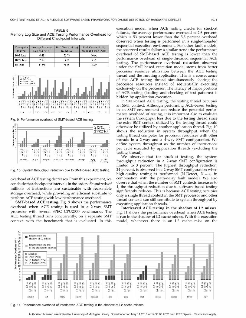
SMT-based ACE testing. Fig. 9 shows the performanceoverhead when ACE testing is used in a 2-way SMTprocessor with several SPEC CPU2000 benchmarks. TheACE testing thread runs concurrently, on a separate SMTcontext, with the benchmark that is evaluated. In this
execution model, when ACE testing checks for stuck-atfailures, the average performance overhead is 2.6 percent,which is 53 percent lower than the 5.5 percent overheadobserved when testing is performed in a single-threadedsequential execution environment. For other fault models,the observed results follow a similar trend: the performanceoverhead of SMT-based ACE testing is lower than theperformance overhead of single-threaded sequential ACEtesting. The performance overhead reduction observedunder the SMT-based execution model stems from betterprocessor resource utilization between the ACE testingthread and the running application. This is a consequenceof the ACE testing thread simultaneously sharing theprocessor resources instead of sequentially executingexclusively on the processor. The latency of major portionsof ACE testing (loading and checking of test patterns) ishidden by application execution.
In SMT-based ACE testing, the testing thread occupiesan SMT context. Although performing ACE-based testingin an SMT environment can reduce the potential perfor-mance overhead of testing, it is important also to evaluatethe system throughput loss due to the testing thread sincethe extra SMT context utilized by the testing thread couldotherwise be utilized by another application thread. Fig. 10shows the reduction in system throughput when thetesting thread competes for processor resources with otherthreads in a 2-way and a 4-way SMT configuration. Wedefine system throughput as the number of instructionsper cycle executed by application threads (excluding thetesting thread).
We observe that for stuck-at testing, the systemthroughput reduction in a 2-way SMT configuration islimited to 3 percent. The highest throughput reduction,24 percent, is observed in a 2-way SMT configuration whenhigh-quality testing is performed (N-Detect, N ¼ 4, incombination with the path-delay fault model). We alsoobserve that when the number of SMT contexts increases to4, the throughput reduction due to software-based testingsignificantly reduces. This is because ACE testing occupiesonly a single thread context in the SMT processor and otherthread contexts can still contribute to system throughput byexecuting application threads.
Interleaved ACE testing in the shadow of L2 misses.Fig. 11 shows the performance overhead when ACE testingis run in the shadow of L2 cache misses. With this executionmodel, whenever there is an L2 cache miss on the
CONSTANTINIDES ET AL.: A FLEXIBLE SOFTWARE-BASED FRAMEWORK FOR ONLINE DETECTION OF HARDWARE DEFECTS 1071
Fig. 9. Performance overhead of SMT-based ACE testing.
Fig. 10. System throughput reduction due to SMT-based ACE testing.
Fig. 11. Performance overhead of interleaved ACE testing in the shadow of L2 cache misses.
TABLE 6Memory Log Size and ACE Testing Performance Overhead for
Different Checkpoint Intervals
Authorized licensed use limited to: University of Michigan Library. Downloaded on May 11,2010 at 14:36:06 UTC from IEEE Xplore. Restrictions apply.

application thread, there is a lightweight context switchwith the ACE testing thread. The application threadresumes execution after the L2 cache miss is served. Inthe case that the checkpoint buffering resources are full(signaling the end of the checkpoint interval) and the ACEtesting is not completed, the ACE testing thread startsrunning exclusively on the processor resources andexecutes the remaining of the ACE testing routine tocompletion. The dark part of each bar in Fig. 11 shows thefraction of ACE testing overhead that is due to testingperformed in the shadow of L2 cache misses, while the graypart shows the fraction of ACE testing overhead that is dueto testing performed at the end of the checkpoint interval.The overhead of testing that is performed in the shadow ofL2 cache misses is caused by the additional time taken toswitch between the application thread and the ACE testingthread, and vice versa.
We observe that for some memory intensive benchmarksthat exhibit a high L2 cache miss rate, such as ammp andmcf, the ACE testing routine was able to run in its entiretyin the shadow of L2 cache misses. For these benchmarks, weobserve an average performance overhead reduction of 57and 43 percent, respectively, compared to single-threadedsequential ACE testing. However, for the rest of thebenchmarks, we noticed that due to the low L2 cache missrate, there were very few opportunities to execute the ACEtesting thread in the shadow of L2 cache misses. Thesebenchmarks, depending on the amount of ACE testingperformed in the shadow of L2 cache misses, exhibit thesame or slightly less performance overhead when com-pared to single-threaded sequential ACE testing.
Based on these experimental results, we conclude thatthe interleaved ACE testing execution model benefits onlybenchmarks that exhibit a high enough L2 cache miss rateand provide enough opportunities for interleaved ACEtesting to utilize the processor resources more efficiently.Different thread interleaving criteria other than L2 cachemisses could lead to higher benefits and affect moreuniformly all benchmarks. However, the overhead ofswitching between the application thread and the ACEtesting thread should be kept low. We leave the design andinvestigation of such criteria and low overhead contextswitching to future work.
5.5 Overhead of ACE Testingin I/O-Intensive Applications
In I/O-intensive applications, frequent I/O operationssignificantly affect the performance overhead of check-point-based system rollback and recovery. Several systemI/O operations are not reversible (e.g., sending a packet to anetwork interface, writing to the display, or writing to thedisk), and thus, cause early checkpoint termination. Conse-quently, frequent I/O operations lead to shorter checkpointintervals and more frequent hardware testing that can havea negative impact on system performance. This sectionevaluates the performance overhead of ACE testing under aheavy I/O usage environment using I/O-intensive filesys-tem and network processing benchmarks.
Fig. 12 shows the execution time overhead of ACEtesting for the stuck-at fault model and the stuck-atcombined with the path-delay fault model. Except forthree of the Netperf benchmarks, all benchmarks exhibit anexecution time overhead that ranges from 4 to 10 percentfor the stuck-at fault model and from 6 to 17 percentwhen combined with the path-delay fault model. Notethat the overheads are very high (greater than 25 percent)
in some Netperf benchmarks because these benchmarks areintentionally designed to stress-test the network interfaceby executing a very tight loop that continuously sends andreceives packets to/from the network interface. Even withthese adversarial benchmarks, the performance overheadof ACE testing is at most 27 percent with the stuck-at faultmodel and 48 percent with the combined stuck-at andpath-delay fault models.
In this experiment, a checkpoint terminates wheneverthere is a write operation to the filesystem or a send/receive operation to the network interface (i.e., an irrecov-erable I/O operation). This assumption is pessimistic. Theexecution time overhead observed in this experiment cansignificantly be reduced with more aggressive and intelli-gent I/O handling techniques like I/O buffering [39] or I/Ospeculation [40], which we do not consider in this work.Furthermore, we note that heavily I/O-intensive applica-tions, such as the Netperf benchmarks, constitute anunfavorable running environment for the ACE testingtechnique due to two reasons. First, if high performanceis desired when running such I/O intensive applications,the system can alternatively reduce the test qualityrequirements of ACE testing (or even completely switch itoff) and trade-off testing quality with performance. Second,we note that such I/O intensive applications have very lowCPU utilization; therefore, there might be little need forhigh-quality, high-coverage ACE testing of the CPU duringtheir execution.
5.6 ACE Tree Implementation and Area Overhead
The area overhead of the ACE framework is dominated bythe ACE tree. In order to evaluate this overhead, weimplemented the ACE tree for the OpenSPARC T1 archi-tecture in Verilog and synthesized it with the SynopsysDesign Compiler. Our ACE tree implementation consists ofdata movement nodes that transfer data from the tree root(the register file) to the tree leaves (ACE segments) and viceversa. In our implementation, each node has four children,and therefore, in an ACE tree that accesses 32 kilobits (about1/8 of the OpenSPARC T1 architecture), there are 42 internaltree nodes and 128 leaf nodes, where each leaf node has four64-bit ACE segments as children. Fig. 13a shows thetopology of the ACE tree configuration, which has theability to directly access any of the 32 kilobits. To cover thewhole OpenSPARC T1 chip with the ACE framework, weused eight such ACE trees, one for each SPARC core. Theoverall area overhead of the ACE framework configuration(for all eight trees) is 18.7 percent of the chip area.
1072 IEEE TRANSACTIONS ON COMPUTERS, VOL. 58, NO. 8, AUGUST 2009
Fig. 12. Execution time overhead of ACE testing on I/O-intensivefilesystem and networking applications.
Authorized licensed use limited to: University of Michigan Library. Downloaded on May 11,2010 at 14:36:06 UTC from IEEE Xplore. Restrictions apply.

In order to contain the area overhead of the ACEframework, we propose a hybrid ACE tree implementationthat combines the direct processor state accessibility of theprevious implementation with the existing scan-chainstructure. In this hybrid approach, we divide the 32 KACE-accessible bits into sixty-four 512-bit scan chains. Eachscan chain has 64 bits that can be directly accessed throughthe ACE tree. The reading/writing to the rest of the bits inthe scan chain is done by shifting the bits to/from the64 directly accessible bits. Fig. 13b shows the topology of thehybrid ACE tree configuration. The overall area overhead ofthe ACE framework when using the hybrid ACE treeconfiguration is 5.8 percent of the chip area.2
5.7 Power Consumption Overheadof the ACE Framework
An important consideration in evaluating the ACE frame-work is the degree to which the extra hardware increasesthe baseline design’s power consumption envelope. Toevaluate this power consumption overhead for our designon Sun’s OpenSPARC T1 chip multiprocessor, we firstestimated the power consumption of the baseline designthat lacks the ACE framework capabilities. We calibratedthe estimated power consumption with actual powerconsumption numbers provided by Sun for each moduleof the chip [32]. After we validated our power estimates forthe baseline OpenSPARC T1 design, we estimated theadditional power required by the ACE framework.
Power estimation methodology. Fig. 14a shows the majordesign components of the OpenSPARC T1 and the metho-dology/tools we used to estimate their power consumption.We estimated the power consumption of the majority ofOpenSPARC T1 modules using the Synopsys PowerCompiler (part of the Synopsys Design Compiler package)and the available RTL code for the design. Each module’sRTL code is synthesized using the Design Compiler. The
resulting gate-level netlist is subsequently analyzed by thePower Compiler to estimate the module’s power consump-tion. To perform the synthesis and power consumptionanalysis, we used the Artisan IBM 130 nm standard celllibrary, characterized at typical conditions of 1.2 V (Vdd)and 25�C average temperature. The average transistorswitching activity factor was set to 0.5.
For modules dominated by SRAM structures, such as theon-chip caches, where logic synthesis and power analysisusing the RTL code is inefficient,3 we used existing toolsdesigned specifically to characterize SRAM modules. Toestimate the power consumption of the L1 and L2 caches,we used the CACTI 4.2 tool [57], a tool with integratedcache performance, area, and power models.
This methodology is sufficient enough to estimate thepower consumption of most of the chip’s logic modules.However, there are parts of the design whose powerconsumption cannot be accurately estimated with thesetools. These include 1) numerous buses, wires, and repeatersdistributed all over the design, which are very hard to modelaccurately using the Design and Power Compilers, unlessthe design is fully placed and routed, 2) I/O pads of the chip.In order to estimate the power consumption of these twoparts, we used values from the reported power envelope ofthe commercial Sun UltraSPARC T1 design [32].
Results. The estimated power envelope for the wholeOpenSPARC T1 chip without the addition of the ACEframework is 56.3 W.4 Fig. 14b shows the power consump-tion for our enhanced OpenSPARC T1 design including theACE framework. The power envelope of the ACE-en-hanced design is 58.5 W, where the power consumption ofthe ACE framework is estimated to be 2.2 W. Thus, theACE framework consumes 4 percent of the design’s totalpower. Our estimation assumes that the ACE framework isenabled all the time while the chip is in operation.However, as illustrated in the previous sections, the ACEframework is actually used during very short testingperiods at the end of each checkpoint interval. Therefore,we expect the actual power consumption and powerenvelope overhead of the ACE framework to be signifi-cantly lower than 4 percent, depending on the frequencyand length of testing (i.e., checkpoint interval size and timespent in testing).
6 OTHER APPLICATIONS OF THE ACE FRAMEWORK
We believe that the ACE framework is a general frameworkthat can be used in several other applications to amortize itshardware cost. We have recently shown that the ACEframework can be utilized for the flexible detection ofhardware design bugs during online operation [11]. In thissection, we describe how the ACE framework can be usedin two other possible applications: post-silicon debuggingand manufacturing testing.
6.1 ACE Framework for Post-silicon Debugging
Post-silicon debugging is an essential and highly resource-demanding phase that is on the critical path of themicroprocessor development cycle. Following producttape-out (i.e., fabrication of the microprocessor design intoa silicon die), the post-silicon debugging phase checks if the
CONSTANTINIDES ET AL.: A FLEXIBLE SOFTWARE-BASED FRAMEWORK FOR ONLINE DETECTION OF HARDWARE DEFECTS 1073
Fig. 14. Power consumption overhead of the ACE framework: (a) Allmajor design components and the methodology/tools used to estimatethe associated power consumption. (b) The power envelope of theOpenSPARC T1 design enhanced with the ACE framework.
3. In logic synthesis, memory elements are synthesized into either latchesor flip-flops. Therefore, SRAM macrocells are implemented using memorycompilers instead of using the conventional logic synthesis flow.
4. Our estimate of the OpenSPARC T1 power is within 12 percent of thereported power consumption of the commercial Sun Niagara design [32].
Fig. 13. ACE tree implementation: (a) Topology of a direct access ACE
tree. (b) Topology of a hybrid (partial direct access, partial scan chain)
ACE tree.
2. We found that the ACE tree’s impact on the processor’s clock cycletime is negligible in both direct access and hybrid implementations.
Authorized licensed use limited to: University of Michigan Library. Downloaded on May 11,2010 at 14:36:06 UTC from IEEE Xplore. Restrictions apply.

actual physical design of the product meets all theperformance and functionality specifications as they weredefined in the design phase. The goal of post-silicondebugging is to find all design errors, also known asdesign bugs, and to eliminate them through design changesor other means before selling the product to the customer[24], [22], [25].
The first phase of post-silicon debugging is to runextended tests to validate the functional and electricaloperation of the design. The validation content commonlyconsists of focused software test programs written toexercise specific functionalities of the design or randomlygenerated tests that exercise different parts of the design.We refer to these test programs as the validation test suite.These tests are applied under different operating conditions(i.e., voltage, clock frequency, and temperature) in order toelectrically characterize the product. When the observedbehavior diverges from the expected prespecified correctbehavior (i.e., when a failure is found), further investigationis required by the post-silicon debugging team. During afailure investigation, the post-silicon debug engineer tries to1) isolate the failure, 2) find the root cause of the failure,and 3) fix the failure, using features hardwired into thedesign to support debugging as well as tools external to thedesign [24].
Motivation. The trends of higher device integration intoa single chip and the high complexity of modern processordesigns make the post-silicon debugging phase a signifi-cantly costly process, both in terms of resources and time.For modern processors, the post-silicon debugging phasecan easily cost $15-20 million and take six months tocomplete [16]. The post-silicon debugging phase is esti-mated to take up to 35 percent of the chip design cycle [8],resulting in a lengthy time-to-market. As the level of deviceintegration continues to rise and the complexity of modernprocessor designs increases [15], this problem will beexacerbated leading to either 1) very expensive and longpost-silicon debugging phases, which would adverselyaffect the processor cost and/or time-to-market or 2) morebuggy designs being released to the customers due to poorpost-silicon debugging [61], [46], which would likelyincrease the fraction of chips that fail in the field.
There are two major challenges in the post-silicondebugging of modern highly integrated processors. First,because the internal signals of the microarchitecture havelimited observability to the testing software, it is difficult toisolate a failure and find its root cause. Second, because thehardware design is not easily or flexibly alterable by thepost-silicon debug engineer, it is difficult to evaluatewhether or not a potential fix to the design eliminates thecause of the failure [25]. Existing techniques that are used toaddress these two challenges are not adequate, as brieflyexplained below.
Traditional techniques used to address the limited signalobservability problem are built-in scan chains [62], [25] andoptical probing tools [63]. Unfortunately, both have sig-nificant shortcomings. The use of built-in scan chains tomonitor internal signals is very slow due to the serial natureof external scan testing [19]. The effectiveness of opticalprobing tools reduces with each technology generation asdirect probing becomes very difficult, if not impossible,with more metal layers and smaller devices [60]. Further-more, it is very hard to integrate these two techniques intoan automated post-silicon debugging environment [60].
The traditional technique used to evaluate design fixesis the Focused Ion Beam (FIB) [24] technique, which
temporarily alters the design by physically changing themetal layers of the chip. Unfortunately, FIB is limited intwo ways. First, FIB typically can only change metal layersof the chip and cannot create any new transistors. There-fore, some potential design fixes are not possible to makeor evaluate using this technology. Second, FIB’s effective-ness is projected to diminish with further technologyscaling as the access to lower metal layers is becomingincreasingly difficult due to the introduction of more metallayers in modern designs [8], [24].
Recently proposed mechanisms try to address thelimitations of these traditional techniques. Specifically,recently proposed solutions suggest the use of reconfigur-able programmable logic cores and flexible on-chip net-works that will improve both signal observability and theability to temporally alter the design [43]. However, thesesolutions have considerable area overheads [43] and still donot provide complete accessibility to all of the processor’sinternal state [43].
Solution—ACE framework for post-silicon debugging.The ACE framework can be an effective low-overheadframework that provides the post-silicon debug engineerswith full accessibility and controllability of the processor’sinternal microarchitectural state at runtime. This capabilitycan be helpful to post-silicon debug engineers in isolatingdesign bugs and finding their root causes. Furthermore, oncea design bug is isolated and its causes have been identified,the ACE framework can be used to dynamically overwritethe microarchitectural state, and thus, emulate a potentialhardware fix. This allows the debug engineer to quicklyobserve the effects of a potential design fix and verify itscorrectness without any physical hardware modification.
Specifically, the event that triggers a failure investigationby a post-silicon debug engineer is an incorrect designoutput during the execution of the validation test suite.However, by just observing the incorrect output, it is veryhard to pinpoint the root cause of the failure. Therefore,further debugging of the failure is required. The first step inthis process is the reproduction of the conditions underwhich the failure occurred. Once the failure is reproduced,debugging tools can be used to analyze the design’s internalstate and pinpoint the design bug. This is where the ACEfirmware could be very useful to a post-silicon debugengineer. The debug engineer can run the ACE firmware asan independent thread (called the ACE debugging thread)that runs in conjunction with the validation test thread toidentify the root cause of the failure and evaluate a potentialdesign fix. We first describe the required extensions to theACE framework to support post-silicon debugging usingthe ACE firmware, then provide a detailed example of howthe debug engineer uses the ACE framework.
ACE instructions for post-silicon debugging. Table 7shows the ACE instruction set extensions that enable thesynchronization between the validation test thread and theACE debugging thread.
The ACE_pause instruction pauses the execution of therunning validation test thread after it is executed for a givennumber of clock cycles and switches execution to the ACEdebugging thread. The execution switch between thevalidation test thread and the ACE debugging thread isscheduled by setting an interrupt counter to the parametervalue of the ACE_pause instruction. This interrupt counterdecrements every clock cycle during the execution of thevalidation test thread. Once the counter becomes zero, theprocessor state and scan state get swapped, thus, taking asnapshot of the running microarchitectural state of the
1074 IEEE TRANSACTIONS ON COMPUTERS, VOL. 58, NO. 8, AUGUST 2009
Authorized licensed use limited to: University of Michigan Library. Downloaded on May 11,2010 at 14:36:06 UTC from IEEE Xplore. Restrictions apply.

validation testing thread into the scan state. In the same clockcycle, execution is switched to the ACE debugging thread.
The ACE_return instruction returns execution fromthe ACE debugging thread to the validation testingthread and swaps the scan state with the processor statein order to restore the microarchitectural state of thevalidation test thread.
Post-silicon debugging example using the ACE frame-work. Fig. 15 shows example of a possible ACE firmwarewritten to perform post-silicon debugging. Suppose thatthe debug engineer runs a validation test program thatfails after 10,000 cycles of execution and the validationengineer suspects that the bug is in the third ACE domainof the core. Fig. 15 shows the pseudocode of the ACEfirmware written to analyze such a failure. The firstportion of the code (Fig. 15-left) pauses the execution ofthe validation test program at the desired clock cycle; thesecond portion (Fig. 15-middle) allows the debug engineerto single-step the execution by one cycle to observe statechanges. Based on the information obtained by runningthese portions of the code, the engineer devises a possiblefix. The third portion of the code (Fig. 15-right) is used bythe engineer to evaluate whether or not the design fixwould result in correct execution. We describe each codeportion of the ACE firmware in detail below.
The debugging process starts with the execution of theACE debugging firmware thread (Fig. 15-left). In thisthread, the first instruction is an ACE_pause instructionthat sets the interrupt counter to the clock cycle in whichdetailed debugging is desired by the post-silicon debugengineer. In the example shown in Fig. 15, the validation testis set to be interrupted at clock cycle 10,000 (assuming thatthis is the phase of the validation test, where the post-silicondebug engineer suspects that the first error occurs). TheACE_pause instruction is followed by an ACE_return
instruction. ACE_return switches execution from the ACEdebugging thread to the validation test thread, and thus, thevalidation test program’s execution begins.
After 10,000 cycles into the execution of the validationtest thread, the validation test thread is interrupted. At thispoint, 1) processor state is swapped with the scan state and2) execution is switched from the validation test thread tothe ACE debugging thread. Once execution is transferredto the ACE debugging thread, the post-silicon engineeruses the ACE framework to investigate the microarchitec-tural state of the validation test thread during clock cycle10,000 (which is stored in the scan state). The examplescenario in Fig. 15 assumes that the suspected bug is in thethird ACE domain of the core. ACE_get instruction readsthe third ACE domain’s microarchitectural state and printsit to the debugging console. We assume that the domain’smicroarchitectural state is checked by the debug engineerand is found to be error free. Therefore, the debugengineer decides to check the domain’s state in the nextclock cycle. In order to step the execution of the validationtest thread for one clock cycle, the interrupt counter is setto one using the ACE_pause instruction, and the valida-tion test thread’s execution is resumed with the executionof the ACE_return instruction (Fig. 15-middle).
After one clock cycle of validation test execution,control is transferred again to the ACE debugging threadand the domain’s new microarchitectural state is checkedby the debug engineer. After inspecting the domain’smicroarchitectural state, the debug engineer finds that thethird bit of the domain’s sixth segment is a control signalthat should be a zero, but instead, it has the value of one.Thus, the engineer pinpoints the root cause of the failure.In order to verify that this is the only design bug thataffects the execution of the validation test thread, and thatfixing the specific control signal does not cause any othererroneous side effects, the debug engineer modifies thedomain’s microarchitectural state and sets the controlsignal to its correct value using the ACE_set instruction(Fig. 15-right). Assuming that the whole validation testtakes 100,000 clock cycles to execute, the debug engineersets the next debugging interrupt to occur after 90,000 clockcycles, which is right after the completion of the validationtest. At this point, the execution is transferred to thevalidation test thread, which runs uninterrupted tocompletion. After completion, the debug engineer checksthe final output to verify that the potential design bug fixled to the correct output and there were not any erroneousside effects due to the introduction of the bug fix. In thecase that the final output is incorrect, a new failureinvestigation starts from the beginning and the debugengineer writes another piece of firmware to investigatethe failure.
We would like to note the analogy between ACEframework-based post-silicon debugging and conventionalsoftware debugging. ACE_pause instruction is analogous tosetting a breakpoint in software debugging. ACE_return isanalogous to the low-level mechanism that allows switchingfrom the debugger to the main program code. Examining thestate of the processor and stepping hardware execution forone cycle are analogous to examining the state of programvariables and single stepping in software debugging.Finally, ACE framework’s ability to modify the state of theprocessor while the test program is running is analogous to asoftware debugger’s ability to modify memory state duringthe execution of a software program that is debugged. Wenote that, similar to a software debugging program, agraphical interface can be designed to encapsulate the post-silicon debugging commands to ease the use of ACEfirmware for post-silicon debugging.
Advantages. The results of the detailed debuggingprocess, demonstrated by the above example, are sometimes
CONSTANTINIDES ET AL.: A FLEXIBLE SOFTWARE-BASED FRAMEWORK FOR ONLINE DETECTION OF HARDWARE DEFECTS 1075
Fig. 15. Example of ACE firmware pseudocode used for post-silicondebugging.
TABLE 7Additional ACE Instruction Set Extensions
for Post-silicon Debugging
Authorized licensed use limited to: University of Michigan Library. Downloaded on May 11,2010 at 14:36:06 UTC from IEEE Xplore. Restrictions apply.

achievable using traditional post-silicon debugging techni-ques that were described previously. However, the use ofthe ACE framework provides a promising post-silicondebugging tool that can ease, shorten, and reduce the costof the post-silicon design process. The main advantages ofACE framework-based post-silicon debugging are thefollowing:
1. It eases the debugging process: ACE framework-based debugging is closer to software, very similarto the software debugging process, and therefore, istrivial to understand and use by the debug engineer.This ease in debugging is achieved by providingcomplete accessibility and controllability of thehardware state to the debug engineer.
2. It can test potential design bug fixes withoutphysically and permanently modifying the under-lying hardware. This reduces both the cost anddifficulty of post-silicon debugging by reducing themanual labor involved in fixing the design bugs.
3. It can accelerate the post-silicon debugging processbecause it does not require very slow proceduressuch as scan-out of the whole microarchitecturalstate or manual modification of the underlyinghardware using the aforementioned FIB techniqueto evaluate potential design fixes.
6.2 ACE Framework for Manufacturing TestingManufacturing testing is the phase that follows chipfabrication and screens out parts with defective or weakdevices. Today, most complex microprocessor designs usescan chains as the fundamental design for test (DFT)methodology. During the manufacturing testing phase,the design’s scan chains are driven by external automatictest equipment (ATE) that applies pregenerated testpatterns to check the chip under test [7]. During themanufacturing testing phase, every single chip has to gothrough this testing process multiple times at differentvoltage, temperature, and frequency levels. Therefore, themanufacturing testing cost for each chip can be as high as25-30 percent of the total manufacturing cost [19].
Motivation. Although this testing methodology servedthe semiconductor industry well for the last few decades, ithas started to face an increasing number of challenges dueto the exponential increase in the complexity of modernmicroprocessors [15], a product of the continuous siliconprocess technology scaling.
Specifically, the external ATE testers have a limitednumber of channels to drive the design’s scan chains dueto package pin limitations [19]. Furthermore, the speed oftest pattern loading is limited by the maximum scanfrequency that is usually much lower than the chip’soperating frequency [19], [7]. The limited throughput of thescan interface between the external tester and the designunder test constitutes the main bottleneck. These limita-tions in combination with the larger set of test patternsrequired for testing modern multimillion gate designs leadto longer time spent on the tester per chip. Even today, theamount of time a chip spends on a tester can be severalseconds [19]. Considering that the amortized testing cost ofhigh-end test equipment is estimated to be at thousands ofdollars per hour [5], [19], the conventional manufacturingtesting process can be very cost-ineffective for micropro-cessor vendors.
Alternative solutions. Logic BIST is a testing methodol-ogy based on pseudorandom test pattern generation andtest response compaction. To speed up manufacturing
testing, logic BIST techniques use the scan infrastructureto apply the on-chip pseudorandomly generated testpatterns and employ specialized hardware to compact thetest responses [7]. Furthermore, the control signals used fortesting are driven by an on-chip test controller. Therefore, aclear advantage of logic BIST over the traditional manu-facturing testing methodology is that it significantly reducesthe amount of data that is communicated between the testerand the chip. This leads to shorter testing times and, as aresult, lower testing cost. Logic BIST also allows themanufacturing test to be performed at-speed (i.e., at thechip’s normal operating frequency rather than the fre-quency of the automatic test equipment), which improvesboth the speed and quality of testing.
Although logic BIST addresses major challenges of thetraditional manufacturing testing methodology, it alsoimposes some new challenges. First, logic BIST requires theon-chip storage of a very large amount of pseudorandomlygenerated test patterns. Second, because logic BIST usespseudorandomly generated test patterns, it often providessignificantly lower fault coverage than that provided by amuch smaller number of high-quality, ATPG-pregeneratedtest patterns [7]. Third, the use of the logic BIST methodologyrequires significantly more stringent design rules thanconventional manufacturing testing [19]. For example, busconflicts must be eliminated and the circuit must be maderandom-pattern testable [19]. Therefore, logic BIST techni-ques significantly increase both the hardware cost and thedesign complexity, while resulting in lower test coverage.
Proposed solution—use of the ACE framework formanufacturing testing. The ACE infrastructure incorpo-rates the advantages of both the scan-based and logic BISTtesting methodologies, while it also can effectively addresstheir limitations. Specifically, the ACE infrastructureprovides two capabilities that are not together present inprevious manufacturing testing techniques. First, the ACEframework is a built-in solution for fast loading of high-quality pregenerated ATPG test patterns into the scan-chain structures through software. This capability caneliminate the need for expensive and slow externalequipment, currently needed for test pattern loading.Second, the ACE framework allows the test patterns to beloaded and applied at-speed at the chip’s normal operatingfrequency rather than the much slower operating fre-quency of the automatic test equipment, which results inhigher quality testing.
With these two capabilities, the ACE framework pro-vides the best of both existing manufacturing testingtechniques: 1) fast loading of test patterns to reduce testingtime, 2) at-speed testing of the chip to improve testingquality as well as to reduce testing time, and 3) testing withATPG-pregenerated test patterns rather than the use ofpseudorandomly generated test patterns, to improve test-ing quality. Thus, if employed by the future integratedcircuit manufacturing testing methodologies, it can greatlyimprove the speed, cost, and test coverage of the costlymanufacturing testing phase of the microprocessor devel-opment cycle.
7 RELATED WORK
Hardware-based reliability techniques. The previouswork most closely related to this work is [50]. In [50],we proposed a hardware-based technique that utilizesmicroarchitectural checkpointing to create epochs ofexecution during which on-chip distributed BIST-liketesters validate the integrity of the underlying hardware.
1076 IEEE TRANSACTIONS ON COMPUTERS, VOL. 58, NO. 8, AUGUST 2009
Authorized licensed use limited to: University of Michigan Library. Downloaded on May 11,2010 at 14:36:06 UTC from IEEE Xplore. Restrictions apply.

To lower silicon cost, the testers were customized to thetested modules. However, this leads to increased designcomplexity because a specialized tester needs to bedesigned for each module.
A traditional defect detection technique that is predomi-nantly used for manufacturing testing is logic BIST [7].Logic BIST incorporates pseudorandom pattern generationand response validation circuitry on the chip. Although on-chip pseudorandom pattern generation removes any needfor pattern storage, such designs require a large number ofrandom patterns and often provide lower fault coveragethan ATPG patterns [7].
This work improves on these previous works due to thefollowing major reasons:
1. It effectively removes the need for on-chip testpattern generation and validation circuitry andmoves this functionality to software;
2. It is not hardwired in the design, and therefore, hasample flexibility to be modified/upgraded in thefield;
3. It has higher test coverage and shorter testing timebecause it uses ATPG instead of pseudorandomlygenerated patterns;
4. In contrast to [50], it can uniformly be applied to anymicroprocessor module with low design complexitybecause it does not require module-specific custo-mizations; and
5. It provides wider coverage across the whole chip,including noncore modules.
Software-based reliability techniques. A very recentapproach proposes the detection of silicon defects byemploying low overhead detection strategies that monitorfor simple software symptoms at the operating system level[33]. These software-based detection techniques rely on thepremise that silicon defects manifested in some microarch-itectural structures have a high probability (�95 percent) topropagate detectable symptoms through the software stackto the operating system [33].
The main differences between [33] and our work are:1) unlike the probabilistic software symptom-based defectdetection, our technique checks the underlying hardware ina deterministic process through a structured high-qualitytest methodology with very high fault coverage (99 percent)and can be executed on demand, 2) software symptom-based defect detection techniques can flag the possibleexistence of a hardware failure, but they do not have thecapability to diagnose which part of the underlying hard-ware is defective. In our technique, by employing ATPG testpatterns, it is trivial to diagnose the defective device at avery fine granularity.
Instruction-based functional testing. A large amount ofwork has been performed in functional testing [6], [26], [31]of microprocessors. The most relevant of these to ourapproach are the instruction-based functional self-testtechniques. In general, these techniques apply randomlygenerated or automatically selected instruction sequencesand/or combinations of instruction sequences and ran-domly or automatically generated operands to test forhardware defects. If the result of the test sequence does notmatch the expected output of the instruction sequence, thena hardware fault is declared.
We briefly describe the state-of-the-art approaches thatwork in this manner: In [58], a self-test program written inprocessor assembly language and the expected results of theprogram are stored in on-chip ROM memory. Wheninvoked, the self-test program performs at-speed functional
testing of the processor. The proposed scheme requires verylittle additional hardware cost. It requires an LFSR forgenerating randomized operands for test instructions and anMISR for generating the result signature. Also, a minormodification of the ISA is required for the test instructions toread/write from the LFSR/MISR. Similarly, Kranitis et al.[29] use the knowledge of the ISA and the RTL-level model ofa processor to select high fault coverage instructions andtheir operands to include in self-test software routines.Batcher and Papachristiou [3] employ instruction randomi-zation hardware to generate randomized instructions to beused in self-test software routines for functional testing.Brahme and Abraham [6] describe how to generate rando-mized instruction sequences to be used in self-test softwareroutines. Building upon these works, Chen and Dey [9]propose a mechanism that generates instruction sequences toexercise structural test patterns designed to test processorcomponents and applies such instruction sequences in thesoftware-based self-test routines to achieve higher coveragethan other approaches that randomly generate instructionsequences.
Our technique is fundamentally different from theseinstruction-based functional testing techniques in that it is astructural testing approach that uses software routines toapply test patterns. We introduce new instructions that arecapable of applying high-quality ATPG-generated structuraltest patterns to every processor segment by exposing the scanchain to the instruction set architecture. Software self-testroutines that use these instructions can therefore directlyapply test patterns to processor structures and read testresponses, which results in the fast and high-coveragestructural testing of each processor component. In contrast,none of the previously proposed instruction-based func-tional testing techniques are capable of directly applying testpatterns to processor components. Instead, they executeexisting ISA instruction sequences to indirectly (functionally)test the hardware for faults. As such, previous instruction-based functional test approaches, in general, lead to highertesting times or lower fault coverage since they rely on(randomized) functional testing.
One recent previous work [41] employed purely soft-ware-based functional testing techniques during the man-ufacturing testing of the Intel Pentium 4 processor. In ourapproach, we use a similar functional testing technique (our“basic core functional test” program) to check the basic corefunctionality before running the ACE firmware to performdirected, high-quality testing. In fact, any of the previouslyproposed instruction-based functional testing approachescan be used as the basic core functional test within the ACEframework.
8 SUMMARY AND CONCLUSIONS
We introduced a novel, flexible software-based technique,ISA extensions, and microarchitecture support to detect anddiagnose hardware defects during online operation of achip-multiprocessor. Our technique uses the Access-ControlExtension (ACE) framework that allows special ISAinstructions to access and control virtually any part of theprocessor’s internal state. Based on this framework, weproposed the use of special firmware that periodicallysuspends the processor’s execution and performs high-quality testing of the underlying hardware to detect defects.We described several execution models for the interactionof the special testing firmware with the applicationsrunning on the processor for both single-threaded andmultithreaded processing cores.
CONSTANTINIDES ET AL.: A FLEXIBLE SOFTWARE-BASED FRAMEWORK FOR ONLINE DETECTION OF HARDWARE DEFECTS 1077
Authorized licensed use limited to: University of Michigan Library. Downloaded on May 11,2010 at 14:36:06 UTC from IEEE Xplore. Restrictions apply.

Using a commercial ATPG tool and three different faultmodels, we experimentally evaluated our ACE testingtechnique on a commercial chip multiprocessor design basedon Sun’s Niagara. Our experimental results showed thatACE testing is capable of performing high-quality hardwaretesting for 99.22 percent of the chip area. Based on ourdetailed RTL implementation, implementing the ACE frame-work requires a 5.8 percent increase in Sun Niagara’s chiparea and a 4 percent increase in its power consumptionenvelope.
We demonstrated how ACE testing can seamlessly becoupled with a coarse-grained checkpointing and recoverymechanism to provide a complete defect tolerance solution.Our evaluation shows that, with coarse-grained checkpointintervals, the average performance overhead of ACE testingis only 5.5 percent. Our results also show that the software-based nature of ACE testing provides ample flexibility todynamically tune the performance-reliability trade-off atruntime based on system requirements.
We also described how the ACE framework can be usedto improve the quality and reduce the cost of two criticalphases of microprocessor development: post-silicon debug-ging and manufacturing testing. Our descriptions showedthat the flexibility provided by the ACE framework cansignificantly ease and accelerate the post-silicon debuggingprocess by making the microarchitecture state easilyaccessible and controllable by the post-silicon debugengineers. Similarly, the flexibility of the ACE frameworkcan eliminate the need for expensive automatic testequipment or costly yet lower coverage hardware changes(e.g., logic BIST) needed for manufacturing testing. Weconclude that the ACE framework is a general frameworkthat can be used for multiple purposes to enhance thereliability and to reduce the design/testing cost of modernmicroprocessors.
ACKNOWLEDGMENTS
The authors thank the anonymous reviewers for theirfeedback. This work was supported by grants from theNational Science Foundation (NSF), SRC, and GSRC, and isan extended and revised version of [12].
REFERENCES
[1] A. Agarwal, B.-H. Lim, D.A. Kranz, and J. Kubiatowicz, “April: AProcessor Architecture for Multiprocessing,” Proc. 17th Ann. Int’lSymp. Computer Architecture (ISCA-17), 1990.
[2] T.M. Austin, “DIVA: A Reliable Substrate for Deep SubmicronMicroarchitecture Design,” Proc. 32nd Ann. Int’l Symp. Micro-architecture (MICRO-32), 1999.
[3] K. Batcher and C. Papachristiou, “Instruction Randomization SelfTest for Processor Cores,” Proc. Very Large Scale Integration (VLSI)Test Symp. (VTS), 1999.
[4] S. Borkar, T. Karnik, and V. De, “Design and ReliabilityChallenges in Nanometer Technologies,” Proc. 41st Ann. Conf.Design Automation (DAC-41), 2004.
[5] B. Bottoms, “The Third Millennium’s Test Dilemma,” IEEE Designand Test of Computers, vol. 15, no. 4, pp. 7-11, Oct.-Dec. 1998.
[6] D. Brahme and J.A. Abraham, “Functional Testing of Micro-processors,” IEEE Trans. Computers, vol. 33, no. 6, pp. 475-485,June 1984.
[7] M.L. Bushnell and V.D. Agrawal, Essentials of Electronic Testing forDigital, Memory and Mixed-Signal VLSI Circuits. Kluwer AcademicPublishers, 2000.
[8] K.-H. Chang, I.L. Markov, and V. Bertacco, “Automating Post-Silicon Debugging and Repair,” Proc. Int’l Conf. Computer-AidedDesign (ICCAD), Nov. 2007.
[9] L. Chen and S. Dey, “Software-Based Self-Testing Methodologyfor Processor Cores,” IEEE Trans. Computer-Aided Design ofIntegrated Circuits and Systems, vol. 20, no. 3, pp. 369-380, Mar. 2001.
[10] K. Constantinides, J. Blome, S. Plaza, B. Zhang, V. Bertacco, S.Mahlke, T. Austin, and M. Orshansky, “BulletProof: A Defect-Tolerant CMP Switch Architecture,” Proc. 12th Int’l Symp. HighPerformance Computer Architecture (HPCA-12), 2006.
[11] K. Constantinides, O. Mutlu, and T. Austin, “Online Design BugDetection: RTL Analysis, Flexible Mechanisms, and Evaluation,”Proc. 41st Ann. Int’l Symp. Microarchitecture (MICRO-41), 2008.
[12] K. Constantinides, O. Mutlu, T. Austin, and V. Bertacco, “Soft-ware-Based Online Detection of Hardware Defects: Mechanisms,Architectural Support, and Evaluation,” Proc. 40th Ann. Int’l Symp.Microarchitecture (MICRO-40), 2007.
[13] W.J. Dally, L.R. Dennison, D. Harris, K. Kan, and T. Xanthopoulos,“The Reliable Router: A Reliable and High-Performance Commu-nication Substrate for Parallel Computers,” Proc. Parallel ComputerRouting and Comm. Workshop (PCRCW), 1994.
[14] N. Durrant and R. Blish, “Semiconductor Device ReliabilityFailure Models,” http://www.sematech.org/, 2000.
[15] M.J. Flynn and P. Hung, “Microprocessor Design Issues: Thoughtson the Road Ahead,” IEEE Micro, vol. 25, no. 3, pp. 16-31, May/June 2005.
[16] R. Goering, “Post-Silicon Debugging Worth a Second Look,”Electronic Eng. Times, Feb. 2007.
[17] R. Guo, S. Mitra, E. Amyeen, J. Lee, S. Sivaraj, and S. Venkatara-man, “Evaluation of Test Metrics: Stuck-At, Bridge CoverageEstimate and Gate Exhaustive,” Proc. Very Large Scale Integration(VLSI) Test Symp. (VTS), 2006.
[18] P. Guptan and A.B. Kahng, “Manufacturing-Aware PhysicalDesign,” Proc. Int’l Conf. Computer-Aided Design (ICCAD), 2003.
[19] G. Hetherington, T. Fryars, N. Tamarapalli, M. Kassab, A. Hassan,and J. Rajski, “Logic BIST for Large Industrial Designs: Real Issuesand Case Studies,” Proc. Int’l Test Conf. (ITC), Sept. 1999.
[20] NetPerf: A Network Performance Benchmark. Hewlett-PackardCompany, 1995.
[21] H. Hirata, K. Kimura, S. Nagamine, Y. Mochizuki, A. Nishimura, Y.Nakase, and T. Nishizawa, “An Elementary Processor Architecturewith Simultaneous Instruction Issuing from Multiple Threads,”Proc. 19th Int’l Symp. Computer Architecture (ISCA-19), 1992.
[22] H. Holzapfel and P. Levin, “Advanced Post-Silicon Verificationand Debug,” EDA Tech Forum, vol. 3, no. 3, Sept. 2006.
[23] A.M. Ionescu, M.J. Declercq, S. Mahapatra, K. Banerjee, and J.Gautier, “Few Electron Devices: Towards Hybrid CMOS-SETIntegrated Circuits,” Proc. Design Automation Conf. (DAC), 2002.
[24] D. Josephson, “The Good, the Bad, and the Ugly of Silicon Debug,”Proc. 43rd Design Automation Conf. (DAC-43), pp. 3-6, 2006.
[25] D. Josephson and B. Gottlieb, “The Crazy Mixed up World ofSilicon Debug,” Proc. IEEE Custom Integrated Circuits Conf.(IEEE-CICC), 2004.
[26] H. Klug, “Microprocessor Testing by Instruction SequencesDerived from Random Patterns,” Proc. Int’l Test Conf. (ITC), 1988.
[27] C. Kong, “A Hardware Overview of the NonStop Himalaya(K10000),” Tandem Systems Overview, vol. 10, no. 1, pp. 4-11, 1994.
[28] P. Kongetira, K. Aingaran, and K. Olukotun, “Niagara: A 32-WayMultithreaded SPARC Processor,” IEEE Micro, vol. 25, no. 2,pp. 21-29, Mar./Apr. 2005.
[29] N. Kranitis, A. Paschalis, D. Gizopoulos, and Y. Zorian, “Instruc-tion-Based Self-Test of Processor Cores,” Proc. Very Large ScaleIntegration (VLSI) Test Symp. (VTS), 2002.
[30] R. Kuppuswamy, P. DesRosier, D. Feltham, R. Sheikh, and P.Thadikaran, “Full Hold-Scan Systems in Microprocessors: Cost/Benefit Analysis,” Intel Technology J., vol. 8, no. 1, pp. 63-72, Feb.2004.
[31] J. Lee and J.H. Patel, “An Instruction Sequence AssemblingMethodology for Testing Microprocessors,” Proc. Int’l (r) Test Conf.(ITC), Sept. 1992.
[32] A.S. Leon, K.W. Tam, J.L. Shin, D. Weisner, and F. Schumacher,“A Power-Efficient High-Throughput 32-Thread SPARC Proces-sor,” IEEE J. Solid-State Circuits, vol. 42, no. 1, pp. 7-16, Jan. 2007.
[33] M.-L. Li, P. Ramachandran, S.K. Sahoo, S.V. Adve, V.S. Adve, andY. Zhou, “Understanding the Propagation of Hard Errors toSoftware and Implications for Resilient System Design,” Proc. 13thInt’l Conf. Architectural Support for Programming Languages andOperating Systems (ASPLOS-XIII), 2008.
1078 IEEE TRANSACTIONS ON COMPUTERS, VOL. 58, NO. 8, AUGUST 2009
Authorized licensed use limited to: University of Michigan Library. Downloaded on May 11,2010 at 14:36:06 UTC from IEEE Xplore. Restrictions apply.

[34] Y. Li, S. Makar, and S. Mitra, “CASP: Concurrent AutonomousChip Self-Test Using Stored Test Patterns,” Proc. Conf. Design,Automation and Test in Europe (DATE), 2008.
[35] C.-K. Luk, R.S. Cohn, R. Muth, H. Patil, A. Klauser, G. Lowney, S.Wallace, V.J. Reddi, and K. Hazelwood, “Pin: Building Custo-mized Program Analysis Tools with Dynamic Instrumentation,”Proc. Conf. Programming Language Design and Implementation(PLDI), 2005.
[36] E.J. McCluskey and C.-W. Tseng, “Stuck-Fault Tests vs. ActualDefects,” Proc. Int’l Test Conf. (ITC), pp. 336-343, Oct. 2000.
[37] M. Meterelliyoz, H. Mahmoodi, and K. Roy, “A Leakage ControlSystem for Thermal Stability during Burn-In Test,” Proc. Int’l TestConf. (ITC), 2005.
[38] S. Mitra, N. Seifert, M. Zhang, Q. Shi, and K.S. Kim, “RobustSystem Design with Built-In Soft-Error Resilience,” Computer,vol. 38, no. 2, pp. 43-52, Feb. 2005.
[39] J. Nakano, P. Montesinos, K. Gharachorloo, and J. Torrellas,“ReViveI/O: Efficient Handling of I/O in Highly-AvailableRollback-Recovery Servers,” Proc. Int’l Symp. High-PerformanceComputer Architecture (HPCA), 2006.
[40] E.B. Nightingale, P.M. Chen, and J. Flinn, “Speculative Executionin a Distributed File System,” ACM Trans. Computer Systems,vol. 24, no. 4, pp. 361-392, Nov. 2006.
[41] P. Parvathala, K. Maneparambil, and W. Lindsay, “FRITS—AMicroprocessor Functional BIST Method,” Proc. Int’l Test Conf.(ITC), 2002.
[42] M. Prvulovic, Z. Zhang, and J. Torrellas, “ReVive: Cost-EffectiveArchitectural Support for Rollback Recovery in Shared-MemoryMultiprocessors,” Proc. 29th Int’l Symp. Computer Architecture(ISCA-29), 2002.
[43] B.R. Quinton and S.J.E. Wilton, “Post-Silicon Debug UsingProgrammable Logic Cores,” Proc. Conf. Field-ProgrammableTechnology (FPT), pp. 241-248, 2005.
[44] J.M. Rabaey, Digital Integrated Circuits: A Design Perspective.Prentice-Hall, Inc., 1996.
[45] J. Renau, B. Fraguela, J. Tuck, W. Liu, M. Privulovic, L. Ceze, S.Sarangi, P. Sack, K. Stauss, and P. Montesinos, “SESC Simulator,”http://sesc.sourceforge.net, 2002.
[46] S. Sarangi, S. Narayanasamy, B. Carneal, A. Tiwari, B. Calder, andJ. Torrellas, “Patching Processor Design Errors with ProgrammableHardware,” IEEE Micro, vol. 27, no. 1, pp. 12-25, Jan./Feb. 2007.
[47] M.J. Serrano, W. Yamamoto, R.C. Wood, and M. Nemirovsky, “AModel for Performance Estimation in a Multistreamed, Super-scalar Processor,” Proc. Seventh Int’l Conf. Modeling Techniques andTools for Computer Performance Evaluation, 1994.
[48] P. Shivakumar, S.W. Keckler, C.R. Moore, and D. Burger,“Exploiting Microarchitectural Redundancy for Defect Tolerance,”Proc. Int’l Conf. Computer Design (ICCD), 2003.
[49] M. Shulz, “The End of the Road for Silicon,” Nature Magazine, June1999.
[50] S. Shyam, K. Constantinides, S. Phadke, V. Bertacco, and T.Austin, “Ultra Low-Cost Defect Protection for MicroprocessorPipelines,” Proc. 12th Int’l Conf. Architectural Support for Program-ming Languages and Operating Systems (ASPLOS-12), pp. 73-82,2006.
[51] D.P. Siewiorek and R.S. Swarz, Reliable Computer Systems: Designand Evaluation, third ed. AK Peters, Ltd., 1998.
[52] D.J. Sorin, M.M.K. Martin, M.D. Hill, and D.A. Wood, “SafetyNet:Improving the Availability of Shared Memory Multiprocessorswith Global Checkpoint/Recovery,” Proc. 29th Int’l Symp. Compu-ter Architecture (ISCA-29), 2002.
[53] J. Srinivasan, S.V. Adve, P. Bose, and J.A. Rivers, “The Impact ofTechnology Scaling on Lifetime Reliability,” Proc. Int’l Conf.Dependable Systems and Networks (DSN-34), 2004.
[54] J.H. Stathis, “Reliability Limits for the Gate Insulator in CMOSTechnology,” IBM J. Research and Development, vol. 46, nos. 2/3,pp. 265-286, 2002.
[55] OpenSPARC T1 Microarchitecture Specification. Sun Microsystems,Inc., Aug. 2006.
[56] TetraMAX ATPG User Guide, version 2002.05. Synopsys, http://www.synopsys.com, 2002.
[57] D. Tarjan, S. Thoziyoor, and N.P. Jouppi, “Cacti 4.0.,” TechnicalReport hpl-2006-86, Hewlett-Packard, 2006.
[58] M.H. Tehranipour, S. Fakhraie, Z. Navabi, and M. Movahedin, “ALow-Cost At-Speed Bist Architecture for Embedded Processorand Sram Cores,” J. Electronic Testing: Theory and Applications,vol. 20, no. 2, pp. 155-168, 2004.
[59] D. Tullsen, S. Eggers, and H. Levy, “Simultaneous Multithreading:Maximizing On-Chip Parallelism,” Proc. 22nd Int’l Symp. ComputerArchitecture (ISCA-22), June 1995.
[60] D.P. Vallett, “Future Challenges in IC Testing and Fault Isolation,”Proc. IEEE Ann. Meeting of Lasers and Electro-Optics Society (LEOS),vol. 2, pp. 539-540, Oct. 2003.
[61] I. Wagner, V. Bertacco, and T. Austin, “Shielding against DesignFlaws with Field Repairable Control Logic,” Proc. 43rd DesignAutomation Conf. (DAC-43), 2006.
[62] T.J. Wood, “The Test and Debug Features of the AMD-K7Microprocessor,” Proc. Int’l Test Conf. (ITC), pp. 130-136, 1999.
[63] W.M. Yee, M. Paniccia, T. Eiles, and V. Rao, “Laser Voltage Probe(LVP): A Novel Optical Probing Technology for Flip-ChipPackaged Microprocessors,” Proc. Int’l Symp. Physical and FailureAnalysis of Integrated Circuits (IPFA-7), 1999.
Kypros Constantinides received the BSdegree in computer science from the Universityof Cyprus, in 2004, and the MS degree inelectrical engineering and computer sciencefrom the University of Michigan, Ann Arbor, in2006. He is currently working toward the PhDdegree in electrical engineering and computerscience at the University of Michigan, Ann Arbor.He is interested in computer architecture re-search with a focus in reliable system design. He
previously worked at Microsoft Research and Intel Corporation. Hereceived the Intel Foundation PhD Fellowship in 2008. He is a studentmember of the IEEE.
Onur Mutlu received the BS degree in computerengineering and psychology from the Universityof Michigan, Ann Arbor, and the MS and PhDdegrees in ECE from the University of Texas atAustin. He is currently an assistant professor ofECE at Carnegie Mellon University. Prior toCarnegie Mellon, he worked at Microsoft Re-search, Intel Corporation, and Advanced MicroDevices. He is interested in computer architec-ture and systems research, especially in the
interactions between languages, operating systems, compilers, andmicroarchitecture. He was a recipient of the Intel PhD Fellowship in2004, the University of Texas George H. Mitchell Award for Excellencein Graduate Research in 2005, the Microsoft Gold Star Award in 2008,and five “Computer Architecture Top Pick” Paper Awards by the IEEEMicro Magazine. He is a member of the IEEE.
Todd Austin received the PhD degree incomputer science from the University of Wis-consin, Madison, in 1996. He is an associateprofessor of electrical engineering and computerscience at the University of Michigan, Ann Arbor.Prior to joining academia, he was a seniorcomputer architect at Intel’s MicroprocessorResearch Labs, a product-oriented researchlaboratory in Hillsboro, Oregon. His researchinterests include computer architecture, compi-
lers, computer system verification, and performance analysis tools andtechniques. He is a member of the IEEE.
Valeria Bertacco received the Laurea degreein computer engineering from the University ofPadova, Italy, and the MS and PhD degrees inelectrical engineering from Stanford Universityin 2003. She is an assistant professor ofelectrical engineering and computer science atthe University of Michigan. She joined thefaculty at Michigan after being at Synopsysfor four years. Her research interests are in theareas of formal and semiformal design verifica-
tion with emphasis on full design validation and digital systemreliability. She is an associate editor of the IEEE Transactions onComputer-Aided Design of Integrated Circuits and Systems and hasserved on the program committees for DAC and ICCAD. She is arecipient of the US National Science Foundation (NSF) CAREERAward and the University of Michigan’s Outstanding AchievementAward. She is a member of the IEEE.
CONSTANTINIDES ET AL.: A FLEXIBLE SOFTWARE-BASED FRAMEWORK FOR ONLINE DETECTION OF HARDWARE DEFECTS 1079
Authorized licensed use limited to: University of Michigan Library. Downloaded on May 11,2010 at 14:36:06 UTC from IEEE Xplore. Restrictions apply.