ieee transactions on biomedical circuits and systems, … · abstract—this paper presents a fully...
TRANSCRIPT

IEEE TRANSACTIONS ON BIOMEDICAL CIRCUITS AND SYSTEMS, VOL. 7, NO. 6, DECEMBER 2013 747
A Fully Intraocular High-Density Self-CalibratingEpiretinal Prosthesis
Manuel Monge, Student Member, IEEE, Mayank Raj, Student Member, IEEE,Meisam Honarvar Nazari, Member, IEEE, Han-Chieh Chang, Member, IEEE, Yu Zhao, Student Member, IEEE,James D. Weiland, Senior Member, IEEE, Mark S. Humayun, Fellow, IEEE, Yu-Chong Tai, Fellow, IEEE, and
Azita Emami, Member, IEEE
Abstract—This paper presents a fully intraocular self-cali-brating epiretinal prosthesis with 512 independent channels in65 nm CMOS. A novel digital calibration technique matchesthe biphasic currents of each channel independently while thecalibration circuitry is shared among every 4 channels. Dual-bandtelemetry for power and data with on-chip rectifier and clockrecovery reduces the number of off-chip components. The rectifierutilizes unidirectional switches to prevent reverse conduction lossin the power transistors and achieves an efficiency . Thedata telemetry implements a phase-shift keying (PSK) modula-tion scheme and supports data rates up to 20 Mb/s. The systemoccupies an area of . It features a pixel size of
and arbitrary waveform generation per channel.In vitro measurements performed on a Pt/Ir concentric bipolarelectrode in phosphate buffered saline (PBS) are presented. Astatistical measurement over 40 channels from 5 different chipsshows a current mismatch with and .The chip is integrated with flexible MEMS origami coils and pary-lene substrate to provide a fully intraocular implant.
Index Terms—Biomedical, calibration, data telemetry, epiretinalprosthesis, implantable biomedical devices, neural interfaces,neural prosthesis, neural stimulator, neurostimulator, powertelemetry, retinal prosthesis, self-calibrating.
I. INTRODUCTION
R ETINAL degenerative diseases such as retinitis pigmen-tosa (RP) and age-related macular degeneration (AMD)
are leading causes of blindness [1], affecting millions world-wide. RP and AMD damage the photoreceptor cells (rods andcones) resulting in profound vision loss, but leave the inner
Manuscript received October 18, 2013; revised December 10, 2013; acceptedDecember 19, 2013. Date of publication January 20, 2014; date of current ver-sion January 28, 2014. This work was supported by NSF Biomimetic Micro-Electronic Systems—Engineering Research Center (BMES-ERC). This paperwas recommended by Associate Editor S. Gambini.M. Monge, M. Raj, M. H. Nazari, H.-C. Chang, Y. Zhao, and A. Emami
are with the Department of Electrical Engineering, California Instituteof Technology, Pasadena, CA 91125 USA (e-mail: [email protected];[email protected]; [email protected]; [email protected]; [email protected]; [email protected]).J. D.Weiland andM. S. Humayun are with the Department of Ophthalmology
and Biomedical Engineering, University of Southern California, Los Angeles,CA 90033 USA (e-mail: [email protected]; [email protected]).Y.-C. Tai is with the Department of Electrical Engineering, California Insti-
tute of Technology, Pasadena, CA 91125 USA, and also with the Departmentof Bioengineering and Mechanical Engineering, California Institute of Tech-nology, Pasadena, CA 91125 USA (e-mail: [email protected]).Color versions of one or more of the figures in this paper are available online
at http://ieeexplore.ieee.org.Digital Object Identifier 10.1109/TBCAS.2014.2298334
Fig. 1. Retinal Prosthesis (Image courtesy of [15]).
retinal cells (bipolar, horizontal and ganglion cells) functional[2]–[4]. Retinal prostheses Fig. 1 aim to restore vision in thesepatients by bypassing the damaged photoreceptors and directlystimulating the remaining healthy neurons. There are three mainapproaches in retinal prostheses which are based on the locationof the electrode array: epiretinal, subretinal and suprachoroidalapproaches. In an epiretinal prosthesis the electrode array isplaced in front of the retina, in a subretinal prosthesis it is placedbetween the retina and the retinal pigment epithelium, and ina suprachoroidal prosthesis it is placed between the choroidaland the sclera. Each method presents different requirements interms of space, medical procedures, and electrode-tissue inter-face [5], and each has its own advantages and disadvantages.Further discussions on these techniques are well summarized in[1], [5]–[20].The prosthesis stimulates the retina using electrical stim-
ulation. Fig. 2(a) shows a model of the stimulator arrayand the electrode-retina interface. This interface presents ahigh impedance as a result of the small size of the electrode
diameter). The stimulator, which can be modeledas a charge-pump, generates a biphasic current waveform tostimulate the retina Fig. 2(b). During the first phase, charge isinjected into the tissue, which changes the membrane potentialof adjacent cells and makes them fire. In the second phase,this charge is removed from the tissue reducing the residualcharge close to zero. This is important because any remaining
1932-4545 © 2014 IEEE. Personal use is permitted, but republication/redistribution requires IEEE permission.See http://www.ieee.org/publications_standards/publications/rights/index.html for more information.

748 IEEE TRANSACTIONS ON BIOMEDICAL CIRCUITS AND SYSTEMS, VOL. 7, NO. 6, DECEMBER 2013
Fig. 2. (a) Model of the stimulator array and electrode-retina interface, whererepresents the double-layer capacitance, the faradaic charge transfer,
and the solution impedance. (b) Stimulation current waveform.
charge beyond tolerable limits can cause electrolysis that mayresult in tissue damage and electrode corrosion. Therefore,charge-balanced stimulation is essential and requires anodicand cathodic currents to be equal. Another significant charac-teristic is the stimulation waveform. The shape and duration ofeach phase, as well as the interphase delay and the period areimportant stimulation parameters. Several studies have shownthat more sophisticated waveforms such as high-frequencypulse trains, asymmetric biphasic pulses, or non-rectangularshapes (Gaussian, linear and exponential), present advantagesover biphasic pulses [21]–[24]. A recent publication [25] hasproved that flexible stimulation such as step-down currentpulse shape can potentially reduce the required voltage compli-ance by 10%-15%. Thus, having a highly flexible stimulationwaveform is desirable and allows further studies in stimulationefficiency, color perception and multi-channel stimulation [5],[24], [26].Recent work on retinal prostheses has shown significant
progress over the past decade. Clinical trials have provento successfully provide visual restoration with an acuity onthe order of 20/1200 to blind patients suffering from retinaldegeneration [1]. Simulation studies in normally sighted sub-jects have predicted that hundreds of channels are needed torestore functional visual perception to a degree that will enabletasks such as reading and face recognition [20]. In recentepiretinal prostheses, the number of electrodes has increasedconsiderably, achieving up to 1024 channels [27] using a 1:4demux scheme and limiting the functionality of the system tobiphasic pulses. However, previous work has used extraocularimplants with a trans-sclera trans-choroid cable to connect theelectrode array to the retina [11], [12], [17], [28]. Although thismethod results in a less invasive surgery [12], this cable cancause infection and low intraocular pressure (hypotony) in thelong term. To avoid the use of such a cable, a fully intraocularimplant is desired. Intraocular coils as well as low power andsmall size electronics are needed. The former requires thedevelopment of high-Q flexible intraocular coils. For the latter,
it is essential to reduce off-chip components such as crystaloscillators and diodes, and to make the chip smaller and lowpower.Initial designs targeted current levels up to 1 mA to ensure
stimulation of retinal cells. For such designs, an output com-pliance of was required [24], [28] due to the highimpedance of the electrode-retina interface Fig. 2(a). Therefore,high-voltage (HV) technologies were used at the expense of areaand power consumption [5], [24], [28]–[30]. Human clinicaltrials have recently shown that implanted electrodes present astimulus threshold as low as for a diameter elec-trode implanted in the macular region [20], [31]. In addition,advances in implant technology promise close placement of theelectrode array and retinal tissue, which can further decrease therequired current. This opens a window for highly scaled tech-nologies to reduce area and power, and to support hundreds offlexible channels for fully intraocular implants.In this work, a fully intraocular high-density self-calibrating
epiretinal prosthesis implemented in 65 nm CMOS is presented.It provides charge-balanced stimulation with highly flexiblewaveforms. It features dual-band telemetry for power anddata, on-chip rectifier and clock recovery, a digital calibrationtechnique to match biphasic stimulation currents, and 512 in-dependent channels capable of arbitrary waveform generation.This paper is organized as follows. Section II describes thesystem architecture. Section III reviews the calibration methodsfor neural stimulators and presents the proposed calibrationscheme. Detailed circuit-level implementation of the proposedself-calibrating stimulator is presented in Section IV. In vitroexperimental results using a Pt/Ir bipolar electrode in PBS andcomparison with the state of the art are presented in Section V.Finally, Section VI summarizes the work presenting the con-clusions.
II. SYSTEM ARCHITECTURE
The system architecture of the fully intraocular implant isshown in Fig. 3. It consists of two intraocular coils, the 65 nmIC, off-chip capacitors, electrode array, and the biocompatibleflexible parylene substrate. Power and data are wirelesslytransmitted to the implant using dual-band telemetry via a pairof inductively coupled coils. The power telemetry operatesat 10 MHz and produces 4 different supplies: forstimulation and for the rest of the system. The datatelemetry recovers the clock from the power signal and pro-duces 160 MHz and 20 MHz clocks. These signals are usedby the phase-shift keying (PSK) receiver to demodulate the20 Mb/s data. The stimulator array presents 512 independentchannels which are grouped into 8 blocks of 16 4-channelstimulators. The global logic receives and demultiplexes thedata to each block, running at 20 MHz.
A. 3-Coil Power Transmission
Fig. 4 shows the 3-coil power transmission scheme [32]. Thetransmitter coil (L1) has an outer diameter (OD) of 42 mm andis placed on external eye-glasses. The buffer coil (L2) is smaller(20 mmOD) and is placed inside contact lenses. The intraocularreceiver coil (L3) is a flexible MEMS origami foil coil. It isplaced in the anterior chamber of the eye after the crystalline

MONGE et al.: A FULLY INTRAOCULAR HIGH-DENSITY SELF-CALIBRATING EPIRETINAL PROSTHESIS 749
Fig. 3. Fully intraocular epiretinal prosthesis system architecture (modified from [26]).
Fig. 4. Three-coil inductive power transmission (modified from [26]).
lens is removed. This imposes hard constrains on its size (OD) and weight ( in saline). The intraocular
coil presents a Q of 24 at 10MHz in air, 10 mg of mass in saline,and a size of 10 mm OD and 1 mm thickness. The distancebetween L1 and L3 and the small size and weight of the latterreduces the coupling coefficient drastically. The insertion ofthe buffer coil enhances coupling coefficients and due toits high Q and close proximity to the eye. This scheme achievesan efficiency of 36% with 1 inch separation in saline, showing a5x improvement over the 2-coil scheme [32]. It is comparable tothe 40% efficiency of the extraocular 2-coil scheme with 18 mmseparation presented in [33]. Capacitors C1, C2 and C3 resonatecoils L1, L2 and L3, respectevely. Further information about the3-coil power transmission scheme can be found in [32].
Fig. 5. Schematic of the power telemetry. DC-DC conversion sequence:, , (modified from [26]).
B. Power Telemetry
The power telemetry Fig. 5 operates at 10 MHz. It consistsof a full-wave rectifier, a positive and a negative bandgap ref-erence, three DC-DC converters and four low-dropout (LDO)regulators. To reduce the number of off-chip components, anon-chip rectifier was implemented to replace the external diodesused in previous designs [5], [11], [17], [28]. It rectifies the in-coming power signal to output which is then used by theDC-DC converters to generate and . These sig-nals are used by the LDO regulators to produce the supplies
and . Reference voltages for the LDO regulatorsare generated by the bandgaps. The rectifier, DC-DC convertersand LDO regulators are optimized for efficiency achieving
, and , respectively, for a total combine effi-ciency of 65%.The schematic of the proposed full-wave rectifier is shown in
Fig. 6(a). In order to increase the efficiency of this stage, twounidirectional switches are used to prevent reverse conductionloss in the power transistors. A comparison between a pass tran-sistor switch and the proposed unidirectional switch Fig. 6(b)shows the advantages of the latter over a traditional implemen-tation. In a pass transistor switch, when ,the transistor M0 is in forward conduction and power is trans-ferred from the input to the output. However, when de-creases lower than while is still low

750 IEEE TRANSACTIONS ON BIOMEDICAL CIRCUITS AND SYSTEMS, VOL. 7, NO. 6, DECEMBER 2013
Fig. 6. (a) Transistor-level schematic of the proposed full-wave rectifier(modified from [26]). (b) Comparison between the pass transistor switch andthe unidirectional switch showing the reduction in reverse conduction loss.
, reverse conduction occurs. This is not desired and re-duces the efficiency of the stage considerably. In the proposedswitch, reverse conduction is minimized by the addition of tran-sistors M1-M3. When , transistors M2 and M3are off and leave transistor M1 on. This transistor shorts thegate of the power transistor M0 to and turns it off. When
, transistors M2 and M3 turn on, turning M0 on byreducing its gate voltage. Therefore, forward conduction occurswhen while reverse conduction is lim-ited to . Simulation results are also shownin Fig. 6(b). A color scheme shows the three regions of opera-tion of the switch: forward conduction, reverse conduction andcut-off. It can be seen that the reverse conduction region is mini-mized when the unidirectional switches are used. This techniqueimproves the efficiency of the stage to more than 80% while de-livering .The DC-DC converters are implemented using charge-pump
circuits. A single stage charge-pump circuit is used to generatewhile two stages of charge-pump are cascaded to gen-
erate and from the output of the rectifier. This lastcharge-pump circuit is shown in Fig. 7(a).The regulator that generates Vdd employs a feed-forward
ripple cancellation scheme and is shown in Fig. 7(b). This tech-nique filters out the input ripples by replicating the same ripples
Fig. 7. Schematics of the (a) charge-pump DC-DC converter that generatesand , (b) feed-forward ripple cancellation LDO regulator that
generates Vdd (modified from [26]), and (c) LDO regulator that generates -Vddand .
at the gate of transistor M1 through the feed-forward path. Re-sistors R1 and R2 set the feed-forward gain to cancel the noisefrom the main signal path. In addition, due to the inherent highbandwidth of the feed-forward configuration, significant PSRRis achieved at high frequencies [34]. To further enhance thePSRR bandwidth, a zero is introduced in the summing ampli-fier to cancel the dominant pole of the system. Three additionalregulators, as shown in Fig. 7(c), are employed to generate -Vddand for the stimulation circuitry.
C. Data Telemetry
The schematic of the data telemetry is shown in Fig. 8(a). Itimplements a pseudo-differential PSK demodulator with gaincontrol and a PLL for clock recovery. The multiplication factorin the PLL allows for the use of the 10 MHz power signal asa reference to generate I/Q 160 MHz clocks for down-conver-sion and a 20 MHz clock for the data slicers. This alleviatesthe need for an external reference which, in previous designs,was provided by an external crystal oscillator [27], [28]. TheLNA Fig. 8(b) is a single-ended cascode amplifier with gaincontrol. The gain control is obtained by a 3-bit programmablebias scheme. These bits modify the transconductance of M1 bychanging its bias voltage and drain current, providing a min-imum gain of 10. The LNA presents a narrow-band inputimpedance at 160MHz set by the capacitor C, the transistor M1,the bias network, and the external coil. The buffer Fig. 8(c) is

MONGE et al.: A FULLY INTRAOCULAR HIGH-DENSITY SELF-CALIBRATING EPIRETINAL PROSTHESIS 751
Fig. 8. Schematic of the (a) data telemetry and clock recovery [26], (b) LNAwith gain control, (c) differential buffer, and (d) passive-mixer.
a hybrid differential common-source/common-drain amplifierwhich improves the voltage-gain to .The output of each buffer is then mixed by a passive-mixerwith the I/Q 160 MHz clocks, respectively. Passive-mixers Fig.8(d) were chosen to reduce power consumption. The size of themixer switches is optimized to minimize the voltage drop andnon-linearity effects. The low-pass filter is added at the outputof the mixer and is implemented by a passive RC-filter. Thelow-power sense amplifier is a standard Strong-Arm latch fol-lowed by a SR latch.Given the following input signals:
(1)
(2)
where A is the amplitude of the received signal and, the datapath produces 2 data streams
(3)
(4)
where . Each data stream supports datarates up to 20Mb/s, for a combine data rate of 40Mb/s, althoughonly 20Mb/s is required for single-chip operation. The datapathand PLL consume 2.3 mA and , respectively.
Fig. 9. (a) Schematic of the global logic and stimulator array showing scanchain connections. (b) Communication protocol for data transmission.
D. Stimulator Array
The stimulator array, shown in Fig. 9(a), is composed of 512independent channels grouped into 8 blocks. Each block con-sists of 16 4-channel stimulators, which are explained in detailin Section III and Section IV. The input of each stimulator is se-rialized and connected to all stimulators in the same block. Thismakes a 256-bit scan chain per block (4-bit per channel). The8 scan chains are connected to the outputs of the global logic.The global logic receives the demodulated data, processes it anddemultiplexes it into 8 bit streams running at 20 MHz. It imple-ments the communication protocol shown in Fig. 9(b). In case ofcommunication error, the whole package is discarded, the scanchains are reset, and all the stimulators receive a zero input.In this work a high resolution current-based stimulation
scheme has been utilized. The voltage-based stimulation tech-nique reported in [35] promises high energy-efficiency, but it ismore suitable for relatively long stimulation pulses (more than8 ms). A global reference current, generated by the bandgap, isdistributed to each stimulator using a tree structure. Cascodecurrent mirrors with transistors biased in strong inversion areused to minimize current variations. Simulation results showedthat the reference current at each 4-channel stimulator has a
while distributing .
E. Multi-Chip Configuration
An additional feature of the system is its capability for 2-chipconfiguration in a Master/Slave fashion. In this case, both coils(power and data) are connected to the master chip which gener-ates the supplies and demodulates the data. In particular, it pro-duces 2 data streams and Fig. 8(a) according to (3)and (4). One of them is used in the master chip while the other issent to the slave chip. The power and data telemetry circuits inthe slave chip are shut down, since it receives the supplies anddata stream from the master chip. Thus, both chips can be inte-grated in parylene to support 1024 independent channels. As thenumber of required electrodes for retinal prosthesis continues toincrease, this technique will allow the use of multiple chips to

752 IEEE TRANSACTIONS ON BIOMEDICAL CIRCUITS AND SYSTEMS, VOL. 7, NO. 6, DECEMBER 2013
configure a network to scale up the number of channels of thedesign with only minor modifications.
III. CALIBRATION METHODS FOR NEURAL STIMULATORS
Matching the current or charge of biphasic stimulation is animportant design consideration in neural implants. Previousstudies in cochlear implants have shown that a residual DCcurrent of more than 100 nA is highly correlated with neuraltissue damage [36] and that this value has been suggested as asafety limit [37]–[39]. However, a safety limit for retinal pros-thesis has not been established yet and it depends on electrodematerial, electrode size and shape, as well as charge density[40], [41].A large DC blocking capacitor in series with the electrode can
reduce the residual DC current to minimal levels [30],but hundreds of capacitors in the nF range are not realizable forretinal prostheses [42]. Simple passive charge-balancing tech-niques rely on shorting the stimulation electrode to the counterelectrode. The effectiveness of this technique depends on theinitial charge imbalance, the time constant associated with theelectrode-tissue interface, and the available time for the dis-charge phase [30]. The charge error after stimulationis caused by the mismatch between anodic and cathodic cur-rents, and the difference between the duration of each phase.For example, a mismatch between stimulation currentsin a 2 ms 100 Hz biphasic pulse with 1 ms duration at eachphase (i.e., pulse duration difference is negligible) generates a
. Assuming there is no interfacedelay, the discharge phase is .For a stimulation period T and a time constant
, where is the shorting switch resistance,is the tissue resistance and represents the double-layer
capacitance of the interface, the net DC current error is definedas
(5)
which is equal to 34.74 nA. Although this value is less than100 nA, for reasons of patient safety, it is desirable to achievea more precise charge balance with a DC current error close tothe level produced by DC blocking capacitors [30]. Therefore, itis important to reduce the initial charge imbalance by matchinganodic and cathodic currents with high precision [5], [24].
A. Previous Work
Several methods to achieve charge-balanced stimulation havebeen reported in the literature. An analog negative feedbacktechnique to sample and hold a correction current to improvecurrent matching has been used in [29]. A similar technique,dynamic current matching, is used in [30]. Here, a single DACgenerates the cathodic current which is sampled by a pmos tran-sistor to produce the anodic current. These schemes require theuse of large capacitors to store the sampled voltage for the dura-tion of both phases. This increases the area of the stimulator con-siderably, making them not suitable for a multi-channel implant.They also need to run for every stimulation which increases the
Fig. 10. Model of the proposed calibration scheme and illustration of the non-ideal initial characteristics of and due to process variation.
power consumption. Furthermore, they rely on constant outputcurrent that limits them to biphasic pulses.Active charge balancers [5], [24] monitor any residual charge
in the tissue after every stimulation and keep this charge withina safety window of . Two different approacheshave been presented: Active charge balancers based on pulseinsertion and based on offset regulation. The former cancels theremaining charge instantaneously via short current pulses [5]while the latter cancels the remaining charge in the long-termby adjusting the offset of the stimulation currents [24], [43]. Theprecision of charge balance in this technique is a function of thecapacitance of the electrode-tissue interface [30]. In addition,this compensation depends on the output waveform and changesfor different wave shapes.In this work, we propose a digital calibration technique to
match anodic and cathodic currents, and to re-duce area and power consumption. The calibration needs to runonly once when the implant is turned on (e.g., daily).
B. Two-Step Digital Calibration Scheme
A model of the stimulator connected to the calibration cir-cuitry is shown in Fig. 10. Two switched resistors are used tosense the output current during calibration. The high re-sistor increases the conversion gain when is low, whilethe low resistor ensures voltage compliance when ishigh. This measured voltage is then compared to toproduce a digital output that is sent to the local logic. Based onthis result, the local logic adjusts two current DACs to calibratethe stimulation currents. As illustrated in the same figure, an-odic and cathodic currents differ from an ideal behavior due toprocess variation. To compensate for this difference, a two-stepdigital calibration scheme is proposed. During the first step, theoffset of , which is the current value at zero input, is can-celled. In the second step, is matched to by reducingtheir difference .1) Step 1: To measure the offset of , is connected
to the output, a zero input is set, and the current sourceis turned on. As a result, the offset of flows to . Thevoltage across this resistor is then compared to .

MONGE et al.: A FULLY INTRAOCULAR HIGH-DENSITY SELF-CALIBRATING EPIRETINAL PROSTHESIS 753
Fig. 11. Conceptual model of the two-step multi-point calibration scheme [26].
Based on this, the calibration current is changed to adjustuntil the comparator switches. Finally, the value of the
calibration DAC is stored in a local register. For this step,is set to to account for the fact that the offset offlows from to the current source making always neg-ative. In order to switch the comparator, is compared to asmall negative voltage so that, when the offset gets reduced, thecomparator switches.2) Step 2: To measure , is connected to the output
and both currents are turned on so that flows to . Usingthe same method as the previous case with set to 0 V (since
can flow in both directions), the calibration current isadjusted to reduce . Then, the calibration value is also storedin a local register.3) Multi-Point Calibration: Since the slope of the two cur-
rents can vary, reducing at one point does not guarantee tomatch them over the entire range. To overcome this issue, theoutput current range is split into regions and a distinct calibra-tion is performed for each region. By increasing the number ofcalibration points, the overall difference of the currents getsreduced over the entire range. In this design, for the target mis-match of that correspond to , a 5-point calibrationscheme was chosen.Fig. 11 illustrates the conceptual model of the calibration
scheme. Simulation results from a Montecarlo simulation areshown in Fig. 12. The calibration scheme was able to adjustthe currents in all cases and achieve significant improvementin matching. The current mismatch after calibration has a mean
of and standard deviation of . Detailsof the implementation and analysis of the effects of process vari-ation in the calibration scheme are explained in Section IV-B.
IV. SELF-CALIBRATING 4-CHANNEL STIMULATOR
The circuit level implementation of the proposed stimulatoris shown in Fig. 13. It consists of 4 independent current drivers,which share calibration circuitry and local logic. Each currentdriver presents a 5 V output stage and produces an arbitraryoutput waveform with 4 bits of resolution at time-steps. A 4-bit input signal determines the input current . Thiscurrent is mirrored to the output stage to produce either the an-odic current or the cathodic current , depending onthe stimulation phase. The local logic controls the stimulationand the calibration. It has a serial interface that enables the use
Fig. 12. Montecarlo simulation of the two-step calibration scheme showing acurrent mismatch with and .
Fig. 13. Detailed schematic of the self-calibrating 4-channel stimulator(modified from [26]).
of simple cascade connections to build the array. It is importantto mention that while the calibration circuitry is shared amongevery 4 channels, each channel is calibrated independently.
A. Current Driver
The schematic of the current driver is shown in Fig. 13. To en-able robust operation with high output voltage, low-headroom
754 IEEE TRANSACTIONS ON BIOMEDICAL CIRCUITS AND SYSTEMS, VOL. 7, NO. 6, DECEMBER 2013
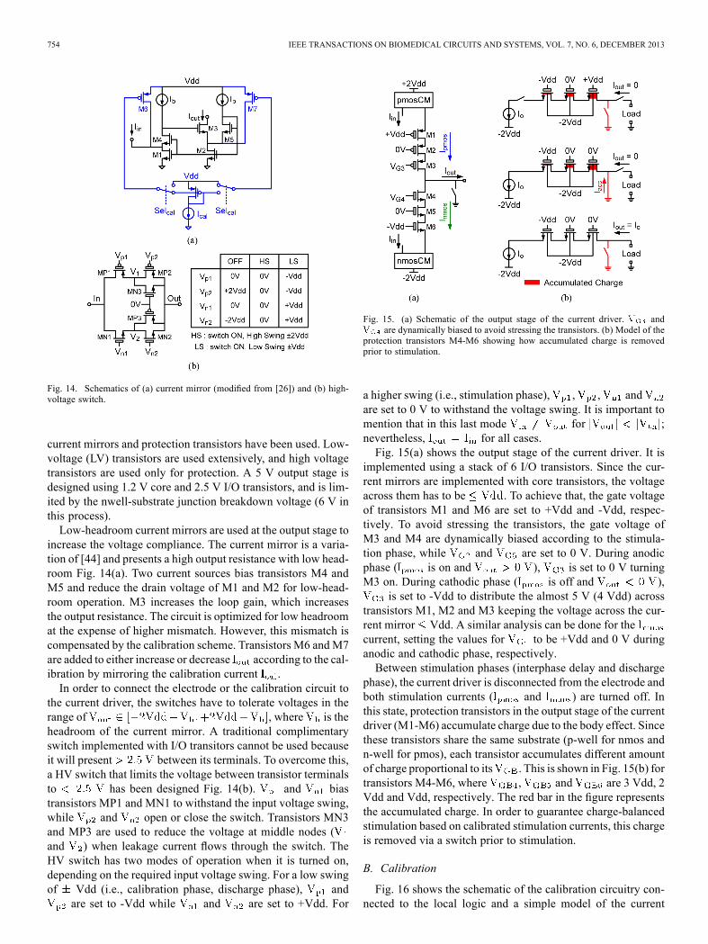
Fig. 14. Schematics of (a) current mirror (modified from [26]) and (b) high-voltage switch.
current mirrors and protection transistors have been used. Low-voltage (LV) transistors are used extensively, and high voltagetransistors are used only for protection. A 5 V output stage isdesigned using 1.2 V core and 2.5 V I/O transistors, and is lim-ited by the nwell-substrate junction breakdown voltage (6 V inthis process).Low-headroom current mirrors are used at the output stage to
increase the voltage compliance. The current mirror is a varia-tion of [44] and presents a high output resistance with low head-room Fig. 14(a). Two current sources bias transistors M4 andM5 and reduce the drain voltage of M1 and M2 for low-head-room operation. M3 increases the loop gain, which increasesthe output resistance. The circuit is optimized for low headroomat the expense of higher mismatch. However, this mismatch iscompensated by the calibration scheme. Transistors M6 and M7are added to either increase or decrease according to the cal-ibration by mirroring the calibration current .In order to connect the electrode or the calibration circuit to
the current driver, the switches have to tolerate voltages in therange of , where is theheadroom of the current mirror. A traditional complimentaryswitch implemented with I/O transitors cannot be used becauseit will present between its terminals. To overcome this,a HV switch that limits the voltage between transistor terminalsto has been designed Fig. 14(b). and biastransistors MP1 and MN1 to withstand the input voltage swing,while and open or close the switch. Transistors MN3and MP3 are used to reduce the voltage at middle nodes (and ) when leakage current flows through the switch. TheHV switch has two modes of operation when it is turned on,depending on the required input voltage swing. For a low swingof Vdd (i.e., calibration phase, discharge phase), and
are set to -Vdd while and are set to +Vdd. For
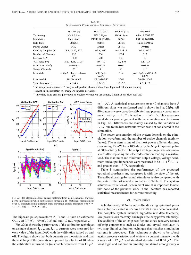
Fig. 15. (a) Schematic of the output stage of the current driver. andare dynamically biased to avoid stressing the transistors. (b) Model of the
protection transistors M4-M6 showing how accumulated charge is removedprior to stimulation.
a higher swing (i.e., stimulation phase), , , andare set to 0 V to withstand the voltage swing. It is important tomention that in this last mode for ;nevertheless, for all cases.Fig. 15(a) shows the output stage of the current driver. It is
implemented using a stack of 6 I/O transistors. Since the cur-rent mirrors are implemented with core transistors, the voltageacross them has to be . To achieve that, the gate voltageof transistors M1 and M6 are set to +Vdd and -Vdd, respec-tively. To avoid stressing the transistors, the gate voltage ofM3 and M4 are dynamically biased according to the stimula-tion phase, while and are set to 0 V. During anodicphase ( is on and ), is set to 0 V turningM3 on. During cathodic phase ( is off and ),
is set to -Vdd to distribute the almost 5 V (4 Vdd) acrosstransistors M1, M2 and M3 keeping the voltage across the cur-rent mirror Vdd. A similar analysis can be done for thecurrent, setting the values for to be +Vdd and 0 V duringanodic and cathodic phase, respectively.Between stimulation phases (interphase delay and discharge
phase), the current driver is disconnected from the electrode andboth stimulation currents ( and ) are turned off. Inthis state, protection transistors in the output stage of the currentdriver (M1-M6) accumulate charge due to the body effect. Sincethese transistors share the same substrate (p-well for nmos andn-well for pmos), each transistor accumulates different amountof charge proportional to its . This is shown in Fig. 15(b) fortransistors M4-M6, where , and are 3 Vdd, 2Vdd and Vdd, respectively. The red bar in the figure representsthe accumulated charge. In order to guarantee charge-balancedstimulation based on calibrated stimulation currents, this chargeis removed via a switch prior to stimulation.
B. Calibration
Fig. 16 shows the schematic of the calibration circuitry con-nected to the local logic and a simple model of the current

MONGE et al.: A FULLY INTRAOCULAR HIGH-DENSITY SELF-CALIBRATING EPIRETINAL PROSTHESIS 755
Fig. 16. Schematic of the calibration circuitry.
Fig. 17. Arbitrary waveform generation.
driver. and sense the output current . A self-bi-ased pmos common-source amplifier with pmos load, imple-mented with I/O transistors, is used as a pre-amplifier to pro-vide gain with good linearity and to bias and protect the com-parator. A strong-arm sense amplifier is used as the calibrationcomparator and is implemented using core transistors. In thisdesign, , , (step 1)or 0 V (step 2), and the calibration DACs have 5-bit resolutionwith set to .The resolution of the calibration is set by the minimum de-
tectable voltage , which is defined as:
(6)
where is the reference current of the calibration DACsand is or , depending on the calibration step. Tomaximize current matching, is designed according to thefollowing expression:
(7)
where
(8)
Thus, the variation of becomes the dominant factor. Thisvariation is minimized by increasing the size of the transistorsin the bias network and by distributing a current that bias these
Fig. 18. Die micrograph of the epiretinal prosthesis, layout of the 4-channelstimulator (4 independent channels sharing local logic and calibration circuitry),and picture of the prototype of the implantable system (modified from [26]).
transistors in strong inversion. The drawback is a slightly higherpower consumption.
C. Local Logic
The local logic controls the calibration and the stimulation,and stores the calibration values. It runs at a low frequency clockof 10 kHz to save power and consumes , which is mostlydue to leakage. It implements six finite state machines (FSM).Four identical FSMs control the current drivers and produce in-dependent channels. A separate FSM controls the calibration ofeach channel which is performed in a serial fashion. Finally, anarbiter controls the global operation of the local logic.Fig. 17 shows how the arbitrary output waveform is gener-
ated. A data sequence with 4 bits of resolution defines the ampli-tude of the waveform every . The first non-zero valuescorrespond to the first phase. Then, a group of zeros sets the in-terphase delay. The next group of non-zero values defines thesecond phase. Finally, after both phases, the last group of zeros(discharge phase) ends the biphasic stimulation and shorts theelectrode to ground. Any remaining charge imbalance is thenremoved during this phase.
V. MEASUREMENT RESULTS
The prototype was fabricated in a 65 nm LP bulk CMOSprocess. The die micrograph and stimulator details are presentedin Fig. 18. The chip occupies an area of , includingthe extra area needed for parylene integration (0.4 mm on thebottom, 0.2 mm on the sides and top). The 4-channel stimulatoroccupies an area of including pads, ESD struc-tures and bypass capacitors, for a pixel size of . Apicture of the prototype of the implantable device is also shownin the same figure.The functionality of the system was verified using a
inner/outer diameter Pt/Ir flat concentricbipolar electrode in 1X PBS solution as a load while the

756 IEEE TRANSACTIONS ON BIOMEDICAL CIRCUITS AND SYSTEMS, VOL. 7, NO. 6, DECEMBER 2013
Fig. 19. Measurement of generated supply voltages.
Fig. 20. (a) Measured data telemetry digital signals at 20 Mb/s. (b) Details ofthe measured signals.
implant receives power and data wirelessly. An arbitrary wave-form generator was used to generate the PSK modulated data,and a signal generator was used to generate the 10 MHz powersignal. The impedance of the electrode-solution interface wasmeasured and fitted to a simple linear model. It shows a solutionresistance of in series with a faraday capacitanceof 160 nF. This impedance is close to the impedance expectedfrom a diameter Pt electrode implanted in the retina,which is 100 nF in series with [45].Fig. 19 shows measurements of power telemetry operating at
10MHz. The rectified voltage and the generated supplieswere measured to be ,
and , respectively. Fig. 20 shows measurements ofdata telemetry. A 20 Mb/s 160 MHz PSK data was sent to thesystem and was correctly demodulated. Fig. 20(a) shows 35 msof the measured transmitted signal (TXdata), received signal
Fig. 21. Measured arbitrary output waveforms using a Pt/Ir flat concentricbipolar electrode in 1X PBS solution as a load while power and data aredelivered wirelessly. (a) Biphasic pulse at 60 Hz with a current mismatch of
. (b) 3 different arbitrary waveforms.
(RXdata) and demultiplexed signal (Demuxed_data, output ofglobal logic). Fig. 20(b) shows details of these signals.Measurements of arbitrary output waveforms are shown in
Fig. 21. The measured voltages show the integrated version ofthe current due to the capacitive effect of the electrode-solutioninterface. First, a biphasic pulse at 60 Hz is generated. Then,three different arbitrary waveforms were sent to the implantusing the same setup. A piecewise-constant pulse (WaveformA), a pseudo-exponential pulse followed by a constant pulse(Waveform B), and an asymmetric biphasic pulse (WaveformC) were tested. Measurements show that the chip is capable ofarbitrary output waveform generation. The charge error afterstimulation has been estimated by calculating the inte-gral of the stimulation current over the duration of the pulse.
MONGE et al.: A FULLY INTRAOCULAR HIGH-DENSITY SELF-CALIBRATING EPIRETINAL PROSTHESIS 757
TABLE IPERFORMANCE COMPARISON — EPIRETINAL PROSTHESIS
Fig. 22. (a) Measurements of current matching from a single channel showinga 10x improvement when calibration is turned on. (b) Statistical measurementover 40 channels from 5 different chips showing a current mismatch with
and [26].
The biphasic pulse, waveform A, B and C have an estimatedof 0.7 nC, 1.09 nC, 0.23 nC and 1.2 nC, respectively.
Fig. 22(a) shows the performance of the calibration techniqueon a single channel. and currents were measured foreach value of the input DAC with the calibration turned on andoff. The figure shows that both currents are monotonic and thatthe matching of the currents is improved by a factor of 10 whenthe calibration is turned on (mismatch decreased from
to ). A statistical measurement over 40 channels from 5different chips was performed and is shown in Fig. 22(b). All40 channels were correctly calibrated and present a current mis-match with and . This measure-ment shows good alignment with the simulation results shownin Fig. 12. Differences are mainly caused by the variation of
due to the bias network, which was not considered in thesimulation.The power consumption of the system depends on the stim-
ulation waveform and the number of active channels (activityfactor). The system is one of the most power efficient designs,consuming 15 mW for a 10% duty cycle, biphasic pulseat 50% activity factor. The output voltage range was also mea-sured after replacing the electrode-solution load by a resistiveload. Themaximum andminimum output voltage, voltage head-room and output impedance were measured to be , 0.1 Vand greater than , respectively.Table I summarizes the performance of the proposed
epiretinal prosthesis and compares it with the state of the art.The self-calibrating 4-channel stimulator is also compared withthe state of the art neural stimulators in Table II. The systemachieves a reduction of 35% in pixel size. It is important to notethat none of the previous work in the literature has reportedstatistical measurements for current matching.
VI. CONCLUSION
A high-density 512-channel self-calibrating epiretinal pros-thesis chip fabricated in 65 nm LP CMOS has been presented.The complete system includes high-data rate data telemetry,low-power clock recovery, and high-efficiency power telemetry.The addition of the on-chip rectifier and clock recovery reduceoff-chip components such as diodes and crystal oscillator. Atwo-step digital calibration technique that matches stimulationcurrents is introduced. This technique is shown to be robustagainst process variation and achieves a current mismatch witha mean of and standard deviation of . Thelocal logic and calibration circuitry are shared among every 4

758 IEEE TRANSACTIONS ON BIOMEDICAL CIRCUITS AND SYSTEMS, VOL. 7, NO. 6, DECEMBER 2013
TABLE IIPERFORMANCE COMPARISON — STIMULATOR IC
channels to reduce power and area. The chip features a pixelsize of resulting in a total area of .It also supports a master/slave configuration which extends thedesign to 1024 channels. The system is integrated with MEMSorigami coils and off-chip capacitors using a biocompatibleflexible parylene substrate. All components fit inside the eyeproviding a fully intraocular implant. In vitro measurementresults conducted on a Pt/Ir concentric bipolar electrode in PBSsolution validated the functionality of the system.
ACKNOWLEDGMENT
The authors acknowledge the contributions of M. Loh andJ. Yoo for insightful technical discussions, A. Wang for assis-tance with the experimental work, and TSMC for chip fabrica-tion.
REFERENCES
[1] K. Mathieson, J. Loudin, G. Goetz, P. Huie, L. Wang, T. Kamins, L.Galambos, R. Smith, J. Harris, A. Sher, and D. Palanker, “Photovoltaicretinal prosthesis with high pixel density,” Nature Photon., vol. 6, no.6, pp. 391–397, May 2012.
[2] S. Y. Kim, S. Sadda, J. Pearlman, M. Humayun, E. d. Juan, B. M.Melia, andW. R. Green, “Morphometric analysis of the macula in eyeswith disciform agerelated macular degeneration,” Retina, vol. 22, pp.471–477, 2002.
[3] F. Mazzoni, E. Novelli, and E. Strettoi, “Retinal ganglion cells surviveand maintain normal dendritic morphology in a mouse model of inher-ited photoreceptor degeneration,” J. Neurosci., vol. 28, pp. 14282–92,2008.
[4] J. L. Stone, W. Barlow, M. Humayun, E. de Juan, and A. Milam, “Mor-phometric analysis of macular photoreceptors and ganglion cells inretinas with retinitis pigmentosa,” Arch. of Ophthalmol., vol. 110, pp.1634–39, 1992.
[5] M. Ortmanns, A. Rocke,M. Gehrke, and H. J. Tiedtke, “A 232-Channelepiretinal stimulator ASIC,” IEEE J. Solid-State Circuits, vol. 42, no.12, pp. 2946–2959, Dec. 2007.
[6] J. Ohta, T. Noda, K. Sasagawa, T. Tokuda, Y. Terasawa, H. Kanda, andT. Fujikado, “A CMOS microchip-based retinal prosthetic device forlarge numbers of stimulation in wide area,” in Proc. IEEE Int. Symp.Circuits and Systems, May 2013, pp. 642–645.
[7] T. Tokuda, Y. Takeuchi, T. Noda, K. Sasagawa, K. Nishida, Y.Kitaguchi, T. Fujikado, Y. Tano, and J. Ohta, “Light-controlled retinalstimulation on rabbit using CMOS-based flexible multi-chip stimu-lator,” in Proc. 31st Annu. Int. Conf. IEEE Engineering in Medicineand Biology Soc., Sep. 2009.
[8] Y. T. Wong, S. C. Chen, Y. A. Kerdraon, P. J. Allen, M. F. Mc-Combe, J. W. Morley, N. H. Lovell, and G. J. Suaning, “Efficacy ofsupra-choroidal, bipolar, electrical stimulation in a vision prosthesis,”in Proc. 30th Annu. Int. Conf. IEEE Engineering in Medicine andBiology Soc., Aug. 2008.
[9] L. H. Jung, N. Shany, T. Lehmann, P. Preston, N. H. Lovell, and G. J.Suaning, “Towards a chip scale neurostimulator: System architectureof a current-driven 98 channel neurostimulator via a two-wire inter-face,” in Proc. 33rd Annu. Int. Conf. IEEE Engineering in Medicineand Biology Soc., 2011.
[10] A. Rothermal, V. Wieczorek, L. Liu, A. Stett, M. Gerhardt, A.Harscher, and S. Kibbel, “A 1600-pixel subretinal chip with DC-freeterminals and supply optimized for long lifetime and highstimulation efficiency,” in Proc. IEEE Int. Solid-State Circuits Conf.Dig. Tech. Papers, Feb. 2008, pp. 144–602.
[11] L. Theogarajan, “A low-power fully implantable 15-Channel retinalstimulator chip,” IEEE J. Solid-State Circuits, vol. 43, no. 10, pp.2322–2337, Oct. 2008.
[12] S. K. Kelly, D. B. Shire, J. Chen, P. Doyle, M. D. Gingerich, S. F.Cogan, W. A. Drohan, S. Behan, L. Theogarajan, J. L. Wyatt, and J.F. Rizzo, “A hermetic wireless subretinal neurostimulator for visionprostheses,” IEEE Trans. Biomed. Eng., vol. 58, no. 11, pp. 3197–3205,Nov. 2011.
[13] H. G. Graf, C. Harendt, T. Engelhardt, C. Scherjon, K. Warkentin, H.Richter, and J. N. Burghartz, “High dynamic range CMOS imager tech-nologies for biomedical applications,” IEEE J. Solid-State Circuits,vol. 44, no. 1, pp. 281–289, Jan. 2009.
[14] J. D. Loudin, S. F. Cogan, K. Mathieson, A. Sher, and D. V. Palanker,“Photodiode circuits for retinal prostheses,” IEEE Trans. Biomed. Cir-cuits Syst., vol. 5, no. 5, pp. 468–480, Oct. 2011.
[15] J. Weiland, W. Liu, and M. Humayun, “Retinal prosthesis,” Annu. Rev.Biomed. Eng., vol. 7, pp. 361–401, 2005.
[16] E. Zrenner, “Will retinal implants restore vision?,” Science, vol. 295,no. 5557, pp. 1022–1025, 2002.
[17] W. Liu and M. Humayun, “Retinal prosthesis,” in Proc. IEEE Int.Solid-State Circuits Conf. Dig. Tech. Papers, Feb. 15–19, 2004, vol.1, pp. 218–219.
[18] J. L. Wyatt, “Engineering development of a subretinal prosthesis,” inProc. 2nd DOE Int. Symp. Artificial Sight, 2005, p. 55.
[19] J. Rizzo, “Retinal prosthesis: An encouraging first decade with majorchallenges ahead,” Ophthalmol., vol. 108, no. 1, pp. 13–14, 2001.
[20] J. Weiland and M. Humayun, “Visual prosthesis,” Proc. IEEE, vol. 96,no. 7, pp. 1076–1084, 2008.
[21] W. M. Grill and J. T. Mortimer, “Stimulus waveforms for selectiveneural stimulation,” IEEE Eng. Med. Biol. Mag., vol. 14, no. 4, pp.375–385, 1995.
[22] A. Wongsarnpigoon, J. P. Woock, and W. M. Grill, “Efficiency anal-ysis of waveform shape for electrical excitation of nerve fibers,” IEEETrans. Neural Syst. Rehabil. Eng., vol. 18, pp. 319–328, Jun. 2010.
[23] M. Sahin and Y. Tie, “Non-rectangular waveforms for neural stimu-lation with practical electrodes,” J. Neural Eng., vol. 4, pp. 227–233,May 2007.

MONGE et al.: A FULLY INTRAOCULAR HIGH-DENSITY SELF-CALIBRATING EPIRETINAL PROSTHESIS 759
[24] E. Noorsal, K. Sooksood, X. Hongcheng, R. Hornig, J. Becker, and M.Ortmanns, “A neural stimulator frontend with high-voltage complianceand programmable pulse shape for epiretinal implants,” IEEE J. Solid-State Circuits, vol. 47, no. 1, pp. 244–256, 2012.
[25] M. E. Halpern and J. Fallon, “Current waveforms for neural stimula-tion-charge delivery with reduced maximum electrode voltage,” IEEETrans. Biomed. Eng., vol. 57, no. 9, pp. 2304–2312, Sep. 2010.
[26] M.Monge,M. Raj, M. H. Nazari, H.-C. Chang, Y. Zhao, J.Weiland,M.Humayun, Y.-C. Tai, and A. Emami-Neyestanak, “A fully intraocular
512-channel self-calibrating epiretinal prosthesisin 65 nm CMOS,” in Proc. IEEE Int. Solid-State Circuits Conf. Dig.Tech. Papers, Feb. 17-21, 2013, pp. 296–297.
[27] K. Chen, Y.-K. Lo, and W. Liu, “A 1024-channel high-compliance-voltage SoC for epiretinal prostheses,” in Proc. IEEE Int.Solid-State Circuits Conf. Dig. Tech. Papers, Feb. 17-21, 2013, pp.294–295.
[28] K. Chen, Z. Yang, L. Hoang, J. Weiland, M. Humayun, and W. Liu,“An integrated 256-Channel epiretinal prosthesis,” IEEE J. Solid-StateCircuits, vol. 45, no. 9, pp. 1946–1956, 2010.
[29] E. K. F. Lee and A. Lam, “A matching technique for biphasic stimula-tion pulse,” in Proc. IEEE Int. Symp. Circuits and Systems, 2007, pp.817–820.
[30] J.-j. Sit and R. Sarpeshkar, “A low-power blocking-capacitor-freecharge-balanced electrode-stimulator chip with less than 6 nA DCerror for 1-mA full-scale stimulation,” IEEE Trans. Biomed. CircuitsSyst., vol. 1, no. 3, pp. 172–183, 2007.
[31] A. Horsager, S. H. Greenwald, J. Weiland, M. Humayun, R. J. Green-berg, M. J. McMahon, G. M. Boynton, and I. Fine, “Predicting visualsensitivity in retinal prosthesis patients,” Invest. Ophthalmol. Vis Sci,vol. 50, pp. 1483–1491, 2009.
[32] Y. Zhao,M. Nandra, C. C. Yu, andY. C. TaI, “High performance 3-Coilwireless power transfer system for the 512-electrode epiretinal pros-thesis,” in Proc. Annu. Int. Conf. IEEE Engineering in Medicine andBiology Soc., 2012, pp. 6583–6586.
[33] K. Chen, Y. K. Lo, Z. Yang, J. Weiland, M. Humayun, and W. Liu,“A system verification platform for high-density epiretinal prostheses,”IEEE Trans. Biomed. Circuits Syst., vol. 7, no. 3, pp. 326–337, Jun.2013.
[34] M. El-Nozahi, A. Amer, J. Torres, K. Entesari, and E. Sanchez-Sinencio, “High PSR low drop-out regulator with feed-forward ripplecancellation technique,” IEEE J. Solid-State Circuits, vol. 45, no. 3,pp. 565–577, Mar. 2010.
[35] S. K. Kelly and J. L. Wyatt, “A power-efficient neural tissue stimulatorwith energy recovery,” IEEE Trans. Biomed. Circuits Syst., vol. 5, no.1, pp. 20–29, Feb. 2011.
[36] R. K. Shepherd, N. Linahan, J. Xu, G.M. Clark, and S. Araki, “Chronicelectrical stimulation of the auditory nerve using noncharge-balancedstimuli,” Acta Otolaryngologica, vol. 119, pp. 674–684, 1999.
[37] R. Shepherd, B. Franz, and G. Clark, “The biocompatibility and safetyof cochlear prostheses,” Cochlear Prostheses, pp. 69–98, 1990.
[38] J. Xu, R. K. Sheperd, R. E. Millard, and G. M. Clark, “Chronic elec-trical stimulation of the auditory nerve at high stimulus rates: a phys-iological and histopathological study,” Hear. Res., vol. 105, no. 1, pp.1–29, 1997.
[39] C. Q. Huang, P. M. Carter, and R. K. Shepherd, “Stimulus inducedph changes in cochlear implants: An in vitro and in vivo study,” Ann.Biomed. Eng., vol. 29, no. 9, pp. 791–802, 2001.
[40] S. F. Cogan, “Neural stimulation and recording electrodes,” Annu. Rev.Biomed. Eng., vol. 10, pp. 275–309, 2008.
[41] S. Negi, R. Bhandari, L. Rieth, R. V. Wagenen, and F. Solzbacher,“Neural electrode degradation from continuous electrical stimulation:Comparison of sputtered and activated iridium oxide,” J. Neurosci.Methods, vol. 186, no. 1, pp. 8–17, 2010.
[42] G. J. Suaning and N. H. Lovell, “CMOS neurostimulation asic with100 channels, scalable output, and bidirectional radio-frequencytelemetry,” IEEE Trans. Biomed. Eng., vol. 48, no. 2, pp. 248–260,Feb. 2001.
[43] K. Sooksood, T. Stieglitz, and M. Ortmanns, “An active approach forcharge balancing in functional electrical stimulation,” IEEE Trans.Biomed. Circuits Syst., vol. 4, no. 3, pp. 162–170, Jun. 2011.
[44] L. F. Tanguay, M. Sawan, and Y. Savaria, “A very-high outputimpedance current mirror for very-low voltage biomedical analogcircuits,” in Proc. IEEE Asia Pacific Conf. Circuits and Systems, 2008,pp. 642–645.
[45] S. Shah, A. Hines, D. Zhou, R. J. Greenberg, M. Humayun, and J. Wei-land, “Electrical properties of retinal-electrode interface,” J. NeuralEng., vol. 4, pp. S24–9, Mar. 2007.
[46] N. Tran, E. Skafidas, J. Yang, S. Bai, M. Fu, D. Ng, M. Halpern, and I.Mareels, “A prototype 64-electrode stimulator in 65 nmCMOS processtowards a high density epi-retinal prosthesis,” in Proc. Annu. Int. Conf.IEEE Engineering inMedicine and Biology Soc., 2011, pp. 6729–6732.
[47] H. Chun, Y. Yang, and T. Lehmann, “Safety ensuring retinal prosthesiswith precise charge balance and low power consumption,” IEEE Trans.Biomed. Circuits Syst., 2013, IEEE Early Access article.
Manuel Monge (S’09) received the B.S. degree(with honors) in electrical engineering from thePontifical Catholic University of Peru (PUCP),Lima, Peru, and the M.S. degree in electrical engi-neering from the California Institute of Technology(Caltech), Pasadena, CA, USA, in 2008 and 2010,respectively.Currently, he is working toward the Ph.D. degree
in electrical engineering at Caltech. His researchinterests are analog and mixed-signal circuits andsystems, with focus on process variation correction,
biomedical circuits and neural interfaces. He spent the summer of 2013 atSamsung Display America Laboratory (SDAL) working on on-chip channelmonitoring circuits for high-speed links.Mr. Monge received the 2008 PUCP Best Student Award and 2008 Fulbright
PeruOpportunity Grant Scholarship. He is recipient of the 2009 Caltech AtwoodFellowship and third place winner of the 2013 Broadcom Foundation UniversityResearch Competition.
Mayank Raj (S’08) received the B.Tech. degreefrom the Indian Institute of Technology (IIT),Kanpur, India, and the M.S. degree in electrical engi-neering from the California Institute of Technology(Caltech), Pasadena, CA, USA, in 2008 and 2009,respectively.Currently, he is working toward the Ph.D. degree at
Caltech. The focus of his current research is high-per-formance mixed-signal integrated circuits for high-speed and low-power optical and electrical intercon-nects. He spent the summer of 2012 at Xilinx Inc.
working on on-chip noise monitoring circuits.Mr. Raj was the recipient of the 2008 Caltech Atwood Fellowship and 2012
Patent Achievement Award from Xilinx Inc.
Meisam Honarvar Nazari (S’08–M’13) receivedthe B.Sc. degree from the University of Tehran,Tehran, Iran, in 2005, the M.A.Sc. degree from theUniversity of Toronto, Toronto, ON, Canada, in2008, and the M.S. and Ph.D. degrees in electricalengineering from the California Institute of Tech-nology (Caltech), Pasadena, CA, USA, in 2009 and2013, respectively.Currently, he is a Postdoctoral Sscholar at Caltech.
The focus of his current research is biomedical mi-crosystems for health care monitoring. He spent the
summer of 2011 at Rambus Inc., where he worked on new equalization tech-niques for high data rate communication links.Mr. Nazari received the University of Toronto Fellowship for Fall 2006 and
an Atwood fellowship for Fall 2008. He was the corecipient of 2008 BrianL. Barge Award for excellence in microsystems integration, 2010 AMD/CICCStudent Scholarship Award, the 2012 Solid-State Circuits Society Award, andthe 2012 Circuits and Systems Society predoctoral scholarship. He was also anNVIDIA 2012 graduate fellowship finalist.
Han-Chieh Chang (S’04–M’13) was born in Taipei,Taiwan, in 1982. He received the B.S. degree inmechanical engineering from National TaiwanUniversity (NTU), Taiwan, and the Ph.D. degree inelectrical engineering from the California Instituteof Technology (Caltech), in 2004 and 2013, respec-tively.He has authored papers in more than 15 tech-
nical publications and has five pending U.S. patentapplications. While pursuing the Ph.D. degree, hewas funded by the National Science Foundation
(NSF), working on the Biomimetic MicroElectronic Systems (BMES) project

760 IEEE TRANSACTIONS ON BIOMEDICAL CIRCUITS AND SYSTEMS, VOL. 7, NO. 6, DECEMBER 2013
collaborated with the University of Southern California, Los Angeles, CA,USA, with emphasis on retinal prosthesis. Since September 2013, he hasheld a postdoctoral position with the Department of Electrical Engineering atCaltech.. His research interests focus on developing innovative MEMS devicesfor medical application using semiconductor processing.
Yu Zhao (S’07) received the B.S. degree (withhonors) in microelectronics from Peking University,Beijing, China, and the M.S. degree in electricalengineering from the California Institute of Tech-nology (Caltech), Pasadena, CA, USA, in 2008 and2009 respectively.While pursuing the Ph.D. degree at Caltech, she
has been working on the wireless power transferscheme for intraocular retinal prostheses, wireless in-traocular pressure sensor, catheter-based impedancesensor for intravascular plaque, and wireless ECG
recording implant for zebra fish. Her research interests focus on developingmicro implants for biomedical applications, which involves front-end sensorfabrication, flexible circuitry design, and assemble wireless power and datatelemetries.
James D.Weiland (SM’08) received the B.S. degreein 1988, M.S. degrees in biomedical engineeringin 1993 and electrical engineering in 1995, and thePh.D. degree in 1997, all from the University ofMichigan, Ann Arbor, MI, USA.After receiving the B.S. degree, he worked four
years in industry with Pratt & Whitney Aircraft En-gines. He joined the Wilmer Ophthalmological In-stitute at The Johns Hopkins University, Baltimore,MD, USA, in 1997 as a Postdoctoral Fellow and, in1999, was appointed an Assistant Professor of Oph-
thalmology at Johns Hopkins. He was appointed Assistant Professor at the Do-heny Eye Institute at the University of Southern California (USC), Los An-geles, CA, USA, in 2001. Currently, he is a Professor of Ophthalmology andBiomedical Engineering at USC. He is Deputy Director of the Biomimetic Mi-croelectronic Systems Engineering Research Center. His research interests in-clude retinal prostheses, neural prostheses, electrode technology, visual evokedresponses, implantable electrical systems, and wearable visual aids for the blind.Dr. Weiland is a Senior Member of the IEEE Engineering in Medicine and
Biology Society, the Biomedical Engineering Society, Sigma Xi, and the Asso-ciation for Research in Vision and Ophthalmology.
Mark S. Humayun (M’97–SM’10–F’12) receivedthe B.S. degree from Georgetown University,Washington, DC, USA, the M.D. degree from DukeUniversity, Durham, NC, USA, and the Ph.D. degreefrom the University of North Carolina, Chapel Hill,NC, USA, in 1984, 1989, and 1994, respectively.He is the Director of the University of Southern
California (USC), Los Angeles, CA, USA, EyeInstitute and the USC Sensory Science Institute,Interim Chair of the Department of Ophthalmologyof USC, current holder of the Cornelius J. Pings
Chair in Biomedical Sciences, and Professor of Ophthalmology and BiomedicalEngineering at USC. His research focuses at the intersection of engineering andmedicine on the development of biomimetic bioelectronics for medical appli-cations with a special focus on ophthalmological and neurological diseases. Heis the founding director of the NSF ERC Biomimetic Microelectronic SystemsEngineering Research Center. He has more than 150 peer-reviewed publica-tions, authored more than 20 book chapters and is listed as an inventor on morethan 100 patents/patents applications. His work has led to the formation ofmultiple start-up companies. He is recognized internationally as the inventorof an artificial bioelectronic retina to restore sight to the blind. The artificialretina called Argus II was recently approved by FDA as the first bioelectronicsretinal implant to restore sight to certain blind patients.Dr. Humayun is a member of the National Academies of Engineering and
the National Academies Institute of Medicine. He was named inventor of theyear by R&D Magazine in 2005. U.S. News and World Report listed him in thetop one percent of ophthalmologists in 2011.
Yu-Chong Tai (M’97–SM’03–F’06) received theB.S. degree in electrical engineering from NationalTaiwan University, Taipei, Taiwan, and the M.S.and Ph.D. degrees in electrical engineering from theUniversity of California, Berkeley, Berkeley, CA,USA, in 1982, 1986, and 1989, respectively.He is currently a Professor of electrical engi-
neering, mechanical engineering, and bioengineeringat the California Institute of Technology (Caltech),Pasadena, CA, USA. He developed the first electri-cally spun polysilicon micromotor at the University
of California, Berkeley. At Caltech, his main research interest is MEMS forbiomedical applications, including lab-on-a-chip and microimplants. He hasauthored more than 300 technical articles in the field of MEMS.Dr. Tai was the recipient of the IBM Fellowship, Ross Tucker Award, Best
Thesis Award (at Berkeley), Presidential Young Investigator Award, PackardAward, and ALA Achievement Award.
Azita Emami (S’97–M’04) received the B.S. degree(with honors) from Sharif University of Technology,Tehran, Iran, and the M.S. and Ph.D. degrees inelectrical engineering from Stanford University,Stanford, CA, USA, in 1996, 1999 and 2004, respec-tively.Currently, she is a Professor of Electrical Engi-
neering at the California Institute of Technology(Caltech), Pasadena, CA, USA. From July 2006 toAugust 2007 she was with Columbia University,New York, NY, USA, as an Assistant Professor in
the Department of Electrical Engineering. She also worked as a ResearchStaff Member at IBM T. J. Watson Research Center, Yorktown Heights, NY,USA, from 2004 to 2006. Her current research areas are high-performancemixed-signal integrated circuits and VLSI systems, with focus on high-speedand low-power optical and electrical interconnects, clocking circuits, biomed-ical implants and sensors, drug delivery systems, and compressed sensing.