ieee transactions on biomedical circuits and systems 1 noise analysis...
TRANSCRIPT

This article has been accepted for inclusion in a future issue of this journal. Content is final as presented, with the exception of pagination.
IEEE TRANSACTIONS ON BIOMEDICAL CIRCUITS AND SYSTEMS 1
Noise Analysis and Performance Comparisonof Low Current Measurement Systems for
Biomedical ApplicationsDongsoo Kim, Member, IEEE, Brian Goldstein, Graduate Student Member, IEEE, Wei Tang, Student Member, IEEE,
Fred J. Sigworth, and Eugenio Culurciello, Senior Member, IEEE
Abstract—In this paper, we report on the noise analysis oflow current measurement systems for biomedical applicationsand their fundamental limits. We analyzed resistive feedback,capacitive feedback and current amplifier circuits for low cur-rent measurement systems. Detailed noise analysis for differentbiomedical applications are presented and matched with mea-surement data using a 0.5- � fabrication process. Based on thetheoretical analysis and the corresponding measurement results,the capacitive feedback system provides better noise performancefor the measurement of low current than the others. The capacitivefeedback circuit is capable of measuring 750 fA RMS at a 10 kHzsampling rate, whereas the resistive feedback provides 4 pA andthe current conveyor provides 600 pA at the same bandwidth. Thispaper provides design guidelines to maximize the performanceof low current measuring system for biomedical instrumentationand to provide the best performance available with CMOS tech-nologies.
Index Terms—Biomedical measurements, capacitive feedback,current conveyor, current measurement, integrator, low currentmeasurement system (LCMS), low noise circuit, noise analysis, re-sistive feedback.
I. INTRODUCTION
I NTEGRATED current measurement systems are becomingextremely important integrated circuit components to in-
terface and study physical phenomena at the sub-micro-scaleand also for biological research and instrumentation [1]. All ofthese current measurements require a compact instrumentationhead-stage with very low input current noise. For example, tomeasure ion channel and membrane protein currents as shownin Fig. 1, an integrated low current measurement system with
Manuscript received July 08, 2011; revised October 18, 2011; accepted March16, 2012. This work was supported by the IEEE, and in part by NSF Award0622133, ONR Award N000140811014, and Peregrine Semiconductors. Thispaper was recommended by Associate Editor M. Stanacevic.
D. Kim was with the Department of Electrical Engineering, Yale University,New Haven, CT 06520 USA. He is now with Aptina Imaging, San Jose, CA95134 USA (e-mail: [email protected]).
B. Goldstein and W. Tang are with the Department of Electrical Engineering,Yale University, New Haven, CT 06520 USA (e-mail: [email protected]; [email protected]).
F. Sigworth is with the Department of Biomedical Engineering, Yale Univer-sity, New Haven, CT 06520 USA (e-mail: [email protected]).
E. Culurciello is with the Department of Biomedical Engineering, PurdueUniversity, West Lafayette, IN 47907 USA (e-mail: [email protected]).
Color versions of one or more of the figures in this paper are available onlineat http://ieeexplore.ieee.org.
Digital Object Identifier 10.1109/TBCAS.2012.2192273
Fig. 1. Examples of biomedical applications include DNA sequencingand patch-clamping using low current measurement systems. All of theseapplications, together with nanoscience large-scale arrays, need to record��� ��� �� currents at 10 kHz or more.
pico-ampere resolution is required, such as commercial patch-clamp amplifiers which can measure a cell membrane’s conduc-tance and are normally used to study the effect of drugs and med-ical treatments on ion channel dynamics. In individual ion-chan-nels, currents of are typical. Patch-clamp experimentsrequire recording bandwidths of 1 to 10 kHz. Another exampleof a low current measurement system (LCMS) is one used inDNA sequencing with a nanopore [2], [3]. When the nanoporeis immersed in a conducting fluid and a potential difference isapplied across it, the conduction of ions through the nanoporegenerates an electric current. When individual DNA bases, de-livered by an enzyme, pass through the nanopore, they modulatethe current through the nanopore, with a range of 10–50 pA.These currents are usually recorded at 10 kHz. Another ap-plication where a LCMS is used is in large-scale nanosensingdevices [4], where low chemical and biological concentrationstranslate in pico-ampere to tens of nano-ampere level currentsthat need to be measured at high rates. The 10 kHz bandwidthmentioned is a lower-bound compromise in order to achieveless noise in the measurement, as more bandwidth is always de-sired when possible. Several low current measurement systemshave been implemented and published in the literature [5]–[13].Low current measurements can be performed with passive com-ponents in shunt or feedback configuration with respect to anactive amplifier. For practical reasons, low current measure-ments can be conducted with capacitors or resistors as passive
1932-4545/$31.00 © 2012 IEEE

This article has been accepted for inclusion in a future issue of this journal. Content is final as presented, with the exception of pagination.
2 IEEE TRANSACTIONS ON BIOMEDICAL CIRCUITS AND SYSTEMS
sensing elements. Inductors can also be used for large AC cur-rents, but are not generally employed in biosensor interfaces fortheir size and the small currents involved [14]. Although theshunt structures provide a simple implementation, they cause ahigh offset voltage error and can not provide a clamping voltage.Therefore, typical systems use an operational amplifier with ca-pacitive [12], [13] or resistive feedback [1] as a head-stage.Another approach is using a current amplifier to amplify theinput current eliminating the noise sources from the followingstages [9], [10], [15]. An ideal low-current measurement systemprovides the following features: measures low-current with themaximum bandwidth and sensitivity available, allows measure-ment of bidirectional currents (sinking/sourcing), and allowscontrol of the voltage at the input node (voltage clamping). Notethat there is always a tradeoff between noise performance andbandwidth [16].
This paper provides an extensive circuits and systems reviewof LCMSs and also summarizes a detailed theoretical analysis oftheir noise performance. The purpose of this paper is to illustratethe proper low-noise design methodology for a state-of-the-artLCMS implemented using current CMOS technologies. We an-alyze and compare three different kinds of integrated low-cur-rent measurement systems: a resistive feedback system, a capac-itive feedback system, and a current amplifier system. Section IIdescribes fundamentals of noise analysis and characteristics ofthe input equivalent circuits used in the previously mentionedapplications. Detailed noise analysis of the resistive feedback,capacitive feedback and current amplifier LCMSs will be dis-cussed in Section III. The noise performance comparison andthe measurement results of the fabricated LCMSs are presentedin Section IV. Finally, the conclusion is provided.
II. NOISE ANALYSIS OF INPUT EQUIVALENT CIRCUITS
A. Conventions on Noise Analysis
In electronic circuits, there are a variety of noise sources thatdegrade the system performance including thermal noise, shotnoise, flicker noise, and environmental noises. Here, we summa-rize our conventions on equations and formulas used throughoutthe paper to model noise in LCMSs. We use conventional for-mulas for shot, flicker and thermal noise found in reference [17].
A high-performance operational amplifier (op-amp) is thefundamental building block for a voltage-clamping currentmeasurement system. The role of the op-amp as a transcon-ductor makes its noise performance critical for the overallnoise performance of the system. An op-amp can be modeledas an input-referred voltage noise source, and a noiselessop-amp. The noise model of the op-amp used in this analysisis given in (1)
(1)
However, the noise model in (1) is complicated by the amountof free parameters and is too difficult to be used for the basic
Fig. 2. Schematic diagram of the equivalent input circuit and the electricalvalues of the equivalent circuit parameters for various biomedical application ofthe low current measurement systems. Cell+Pipette: whole-cell recording usinga micropipette [20], [21], Patch+Pipette: patch-clamp recording using a stan-dard glass micropipette [20], [21], Cell+Planar: whole-cell planar patch-clamprecoding [22], DNA: DNA nanopore sequencing [2], [23]. Current ranges andthe sampling frequencies can be different by systems and specified materialsto be measured, lower current range and higher sampling frequency are alwaysunder research.
equation of more complicated circuits. Therefore, we use thesimplified as follows:
(2)
where is the summed coefficient of the thermal noises,and is the summed coefficient of the flicker noisesin the op-amp. This simplified equation is used for noiseanalysis throughout the rest of this paper. From the exper-imental result with the fabricated op-amp, the coefficients,
can be calculated based on Silicon-on-Sapphire (SOS)process which is used for different systems to be compared inthis paper.
B. Equivalent Input Circuit
LCMSs are designed to measure an input current, , withminimum readout current noise. The equivalent input circuitmodel widely used in biological measurement from cell mem-branes or nanopores is given in Fig. 2. As can be seen in Fig. 2,a complex impedance model is always present between andthe measurement system. This is the impedance of the biolog-ical preparation, solutions and measuring electrodes. This inputcircuit can not only generate considerable input noise, but alsochanges the overall system performance of the LCMS which af-fects the noise performance of the system, therefore it is impor-tant to analyze it together with the entire measurement system.Typically, an electrode is used to access the electrical measure-ment from cells or tissue, and therefore an access series resis-tance, , and parasitic capacitance of the electrode at the inputnode of the LCMS, , are presented in the electrical equiva-lent input model. In parallel to , a cell or tissue capacitance,
, is present. In addition, a shunt resistance, , is the off re-sistance of the cell or tissue. directly affects the minimumcurrent measurable, as it produces a leak shunt current. Morecomplex models targeted to limitations of biosensors in aqueous

This article has been accepted for inclusion in a future issue of this journal. Content is final as presented, with the exception of pagination.
KIM et al.: NOISE ANALYSIS AND PERFORMANCE COMPARISON OF LOW CURRENT MEASUREMENT SYSTEMS 3
Fig. 3. Electrical characteristic of various cells, membranes and electrodes:Noise spectral density function of the input equivalent circuits.
solutions are available in the literature [18], [19], but are not rel-evant here, because the complex electrode model is too compli-cated when it is combined with measurement system analysis.Therefore the simple models provided here capture all essentialnoise components for this paper and analysis.
Typical electrical parameter values of the equivalent elec-trical input circuit for common biomedical applications suchas whole-cell recording using a micropipette, patch-clamprecording using a micropipette, whole-cell planar patchrecording, and DNA nanopore sequencing are given in the tableof Fig. 2.
The equivalent impedance of the equivalent input circuit,is defined as
(3)
where is ignored in DNA the nanopore case.The power spectral density (PSD) of the current noise at ,
can be calculated as
(4)
We have analyzed the magnitude of the admittance ofthe input equivalent circuits for various cell membranesand nanopores. The noise spectral density of their compleximpedance are presented in Fig. 3. The input equivalent circuitnot only generates considerable noise, but also modifies thefrequency response of the input-referred noise source of theop-amp, , by the admittance. The cell capacitance, ,and the parasitic capacitance, , increase the magnitude ofthe admittance at higher frequencies. Thus, the multiplicationof the admittance and the input referred noise of the op-ampresults in an overall input-impedance current noise which has tobe much smaller than the input current . The DNA nanoporecase is the most challenging application analyzed here, due tothe large cell membrane capacitance.
Fig. 4. Schematic of the low current measurement circuit with resistive feed-back.� is the equivalent input impedance described in Section II-B.
III. DETAILED NOISE ANALYSIS OF VARIOUS LOW CURRENT
MEASUREMENT SYSTEMS
In this section we will analyze three different low-currentmeasurement systems, based on different headstage circuits. InSection III-A we will present a low-current measurement systemwith resistive feedback, in Section III-B with capacitive feed-back, and in Section III-C a system with a current conveyor as aheadstage. In all of these systems, we assume that the goal is tomeasure an input current, , and also provide a voltage con-trol, , to the input current terminal. We also take into accountthe input impedance model described in Section II-B.
A. Low-Current Measurement With Resistive Feedback
The most typical continuous-time current-mode interface is aresistive feedback trans-impedance amplifier (TIA) based on anoperational amplifier headstage [24]–[26]. The resistive feed-back TIA is presented in Fig. 4 together with the input equiva-lent circuit. The operational amplifier input configuration allowsto concomitantly record input currents and also clamp the inputvoltage, . The input is provided through the negative opera-tional amplifier terminal and the voltage-clamp is provided bythe virtual short between the two input terminals of the opera-tional amplifier in this configuration. The offset voltage causedby the op-amp itself can be considered part of the offset of theclamping voltage, , and it can be removed by offset subtrac-tion. However the change of the clamping voltage due to thefinite gain of the op-amp affects the measurement and it is diffi-cult to remove. The resistive feedback TIA output can measurethe input current by means of the relation
(5)
The noise model for the low current measurement systemwith resistive feedback is presented in Fig. 5 [26]. The noisesources of the resistive feedback system are the feedback re-sistor and the transistors in the op-amp, and the input impedancepresented in the previous section. The output power spectraldensity, , of the current measuring TIA is given by the equa-tion below
(6)
where is the input referred noise of the op-amp including thethermal and flicker noises, is the thermal noise of the feed-back resistor, , and is the admittance of the equivalentinput circuit (cells, membranes and tissues). Note that in this

This article has been accepted for inclusion in a future issue of this journal. Content is final as presented, with the exception of pagination.
4 IEEE TRANSACTIONS ON BIOMEDICAL CIRCUITS AND SYSTEMS
Fig. 5. Noise model for the resistive feedback system.
Fig. 6. Current noise spectral density caused by the feedback resistor and theintrinsic op-amp noise in the resistive feedback system for the application inDNA nanopore sequencing.
theoretical analysis we neglect to include the shot noise contri-bution of the input current to only focus on computing the addednoise from electrodes and circuits. We will add shot noise con-tributions to the model to match with real-case measurements inSection IV.
From the above equations, the power spectral density of theinput referred current noise, , can be obtained (7), dividing
by
(7)
Fig. 6 presents the power spectral response (7) from aLCMS system used for patch-clamp experiments and with a
feedback resistor [25]. The dominant noise sourceat lower frequencies is the thermal noise of the feedback resistorand the input referred op-amp noise reflected in the admittanceof the equivalent input circuit. Notice that this is the highestnoise component above 10 kHz. The total input-referred cur-rent noise of the low-current measurement system with resistivefeedback in Fig. 6 includes the equivalent input circuit of theDNA nanopore (4), and the feedback resistor and the op-ampintrinsic noise (7).
The noise model of the resistive feedback system is matchedwith the experimental results as follows Fig. 7 (the solid linein Fig. 4 is the dotted line in Fig. 7 as theoretical input re-ferred current noise). This data was collected by a resistive trans-
Fig. 7. Current noise spectral density or a resistive feedback LCMS. The theo-retical analysis matches the measured results from a fabricated prototype [26],[27] with � � � �� and � � �� ��.
Fig. 8. Schematic of the low current measurement circuit with capacitive feed-back.
impedance amplifier previously published [27], and an input cir-cuit with and .
B. Low-Current Measurement With Capacitive Feedback
A current integrator circuit can be used for low-current in-tegrated measurement systems with larger bandwidth, becausethe resistive feedback system has a limited bandwidth due tothe big feedback resistor which is one of the dominant noisesources. Several implementations of current integrators havebeen proposed as potentiostats [6], [8], [28]–[30], but none ofthese provided matching measured noise results to confirm thenoise models. This is one of the goals of this paper. Reference[8] provides a noise model that is similar to what is providedhere.
The integrator, portrayed in Fig. 8, is a high gain amplifierwith a shunt integrating capacitor, , between its input andoutput terminals. The output voltage of the current integrator isproportional to the integration time and the input current.
Every time the capacitive feedback system is sampled, its op-eration can be divided in two phases: the andphases. In order to analyze in detail the noise performance ofthe capacitive feedback LCMS we need to separately calculatethe noise for both of these operation phases. Here we ignore theswitching noise of the feedback capacitor ( noise) and as-sume this is canceled by correlated double sampling (CDS). Butnotice that the use of CDS will double the reset thermal noiseand any integration thermal noise.

This article has been accepted for inclusion in a future issue of this journal. Content is final as presented, with the exception of pagination.
KIM et al.: NOISE ANALYSIS AND PERFORMANCE COMPARISON OF LOW CURRENT MEASUREMENT SYSTEMS 5
Fig. 9. Noise model for the capacitive feedback system during the reset phaseand the integration phase. (a) Reset phase. (b) Integration phase.
During the phase, the feedback capacitor’s terminalsare shorted, configuring the op-amp as a voltage follower, asshown in Fig. 9. Thus, the only noise source is the operationalamplifier . In this phase, the voltage power spectral densityof the output equivalent voltage noise, is calculated as
(8)
where is the input referred noise of the op-amp. The equiva-lent input referred current noise, related with the feedbackcapacitance and the integration time can be obtained as
(9)
After reset, the feedback capacitor initial charge is zero.During the phase, the feedback capacitor inte-grates the input current, and the integrated output voltage duringan integration time, , can be represented by a convolutionwith the current and a rectangular time pulse.
The Laplace transform of can be obtained as
(10)
where .The frequency response of the capacitive integrator during an
integration time is shown in Fig. 10. The response duringthe finite time is the combination of two terms: the current in-tegration on the capacitor assuming infinite time (1/s) and the(1—exponential) term. The plot shows both the 1/s term andalso the second term with two values of : 1 ms and .The final frequency response (solid trace with )is similar to a single-pole low-pass-filter.
From (10), the power spectral density of the output, , iscalculated as
(11)
where is the admittance of the equivalent input circuit, .From the above equations, the input referred current noise
during integration, , is
Fig. 10. Frequency response of the capacitive integrator � ��� during an in-tegration time, � (solid trace with � � ��� ��). The response duringthe finite time is the combination of two terms: the current integration on the ca-pacitor assuming infinite time (1/s) and the 1—exponential term, here presentedwith two values of � : 1 ms and ��� ��.
Fig. 11. Current noise spectral density of the integration phase for capacitivefeedback system with different sampling frequencies, � .
(12)
The input referred current noise during integration, ,is plotted in Fig. 11 for a sampling frequency, , of 100 Hz,1 kHz, 10 kHz and 100 kHz.
The total input referred noise, of the capacitive feedbackmeasurement system is approximated as the sum of the noisecurrent power spectral densities of the reset phase and the inte-gration phase including the noise of the input equivalent circuit:
. The noise components and the totalnoise is plotted in Fig. 12.
When a integrated system is implemented with a switch ca-pacitor circuit, the performance is degraded by switching ef-fects including clock feedthrough, charge injection, and KT/Cnoise. The correlated double sampling can eliminate effectivelythe degradation caused by the offsets (clock feedthrough, signalindependent charge injection and KT/C) and the low frequencynoises. A common CDS circuit is presented in Fig. 13(a), it isconnected with the integrator. In high phase of p1 signal, theCDS circuit samples the reset output voltage of the integrator.The integrated signal is subtracted with the stored reset value

This article has been accepted for inclusion in a future issue of this journal. Content is final as presented, with the exception of pagination.
6 IEEE TRANSACTIONS ON BIOMEDICAL CIRCUITS AND SYSTEMS
Fig. 12. Total current noise spectral density for capacitive feedback systemwith � � ��� ��.
Fig. 13. Schematic diagram of a CDS circuit and waveforms. (a) Schematic ofa Correlated Double Sampling (CDS) Circuit. (b) Waveform.
to get the pure integrated signal in the next phase. The outputsignal of the integrator (input of CDS circuit), includesthe noiseless signal and a noise signal . When thereset voltage is sampled in the capacitor in the very short phaseof the sampling, the stored noise voltage of the sampling capac-itor, can be represented as
(13)
where is the unit step function. When the only noise com-ponent of the signal, after CDS is defined as , canbe presented as
(14)
The Fourier Transform, of and are and, respectively. Equation (14) is calculated as follows:
(15)
Fig. 14. Schematic of low current measurement circuit with current conveyor.
Based on the properties of the Fourier Transform [31], (15)can be calculated as
(16)
(17)
where
ifif
When CDS is applied with the capacitive feedback system,the low frequency noise (flicker noise) is reduced by the subtrac-tion operation. Whereas the effect of the flicker noise is dramat-ically reduced by CDS, the thermal noise is increased becausethe thermal noise is not correlated and the noise is doubled bythe subtraction. Therefore, it is important to design the op-ampto have low noise at high frequencies by reducing the thermalnoise of the transistors in order to implement an LCMS that hashigh performance.
C. Low-Current Measurement With Current Conveyor
A current conveyor circuit can amplify low current while ap-plying voltage biases for biosensor interfaces [7], [32]. Fig. 14presents a schematic of a typical current conveyor used for mea-suring small currents without the use of operational amplifiers.
The current conveyor circuit performs decoupling and linearoperations in current mode in the same way that the operationalamplifier performs in voltage mode. The conveyor can decouplethe input current and give current amplification, allowing de-signers to relax both the noise and performance specifications ofthe following measuring stages. Because the potential of node Xis the same with that of node Y, the current conveyor can apply aclamping voltage as is necessary to measure low currents [33].Notice that the output is a current instead of a voltage, unlikeresistive or capacitive feedback systems. Alternatively, if a cur-rent mode analog-to-digital convertor (ADC) is used, the currentconveyor can perform low-current measurements without addi-tional circuits.
A schematic of the current conveyor circuit is given inFig. 15. For simplicity all devices have the same size: W, L(width, length) in the input stage and , L in the outputstage. If a potential is applied to terminal X, the same potentialappears on terminal Y. The current following into terminal X

This article has been accepted for inclusion in a future issue of this journal. Content is final as presented, with the exception of pagination.
KIM et al.: NOISE ANALYSIS AND PERFORMANCE COMPARISON OF LOW CURRENT MEASUREMENT SYSTEMS 7
Fig. 15. Schematic circuit of a current conveyor. The input stage implementstwo latched current mirrors both with PMOS and NMOS transistors. The outputstage can provide amplification if the transistor widths are larger than the inputones.
will be conveyed into terminal Z with high output impedance.The potential at X is independent of the current flowing and anycurrent flowing into X will flow into Y as well. By inspectingFig. 15 one can easily determine that all of the above conditionsare satisfied by the nature of the input stage and its currentmirrors.
The circuit is operated with X as the input port and Z as theoutput port. Z will act as a current source mirroring the valueof the current into X. The output current from Z can be mea-sured by means of the integrative or continuous head stages.Notice that the input current can be amplified using this circuitby making the output stage transistors (right-most transistors inFig. 15) a factor times wider than the input stage transistors:
. Multiple current mirror stages can also be cascadedto obtain large amplifications of the input current.
Since the input and output of the current conveyor are cur-rents, the input referred current noise can be calculated as
(18)
(19)
where is transconductance of transistors in the input stageis current amplification factor.
We have fabricated a current conveyor circuit in asilicon-on-sapphire (SOS) technology. Fig. 16 presents thematching results between the theoretical analysis and measuredresult. The device reported an rms current noise of 750 pA witha bandwidth of 10 kHz. All parameters in (19) were extractedfrom the SOS process manual and simulator [14]. This result issimilar to the data reported with a lower-noise current conveyor
Fig. 16. Current noise spectral density of the current conveyor LCMS. The the-oretical noise analysis matches the measured results from an fabricated devicein a SOS ��� �� process.
circuit based on operational amplifiers [7]. In the current con-veyors, the input signal current from the sensor is merged withthe bias current of the conveyor itself. At this point the noise isthe overall noise resulting from the sum of the sensor currentplus conveyor bias current. Therefore the total noise is hugecompared to the resistive or capacitive feedback system whichhave noise from the sensor alone. For this reason this circuit isnot generally used in very low-current measurement systems.
IV. NOISE PERFORMANCE COMPARISON OF THE LOW-CURRENT
MEASUREMENT SYSTEMS AND THEIR MEASURED RESULTS
We have fabricated and tested all three different low-currentmeasurement systems presented in Sections III-A–III-C. Low-current measurement systems with resistive feedback [24], [25],capacitive feedback [34]–[37], and a current conveyor [14] werefabricated and tested, and the noise performance of each wasreported.
Fig. 17 reports the comparison of the theoretical noise per-formance of low-current measurement systems for the applica-tions presented in Section II-B. Fig. 17(a) is for whole-cell (nAlevel currents) patch-clamping using a pipette electrode [20],[21], Fig. 17(b) is for patch-clamping with a pipette and pico-ampere level currents [20], [21], Fig. 17(c) is for whole-cellpatch-clamping with a planar low-noise electrode [22], and Fig.17(d) is for the DNA nanopore sequencing applications withpico-ampere current levels [2]. As can be seen in Fig. 17, thedifferent characteristics of the input equivalent circuit generatedifferent noise responses for each LCMS. The most importantresult of this paper is that, overall, the current conveyor showsthe worst performance across all applications, while the resis-tive and capacitive feedback case provide state-of-the-art perfor-mance, with the capacitive system being slightly better in eachcase. When used in patch-clamp recording and DNA sequencingapplications, both requiring pico-ampere level measurements,the capacitive feedback system is better than the resistive feed-back system. Moreover, the capacitive feedback system is muchbetter when used for whole-cell planar patch-clamping, due tothe reduced noise of the input admittance in this input config-uration. For whole-cell patch-clamping, the performance of thecapacitive feedback and the resistive feedback are similar when

This article has been accepted for inclusion in a future issue of this journal. Content is final as presented, with the exception of pagination.
8 IEEE TRANSACTIONS ON BIOMEDICAL CIRCUITS AND SYSTEMS
Fig. 17. Current noise spectral density comparison for resistive feedback, capacitive feedback (using CDS), and current conveyor system on various applica-tions, based on the low noise op-amp with the thermal noise level of about � ���
���. (a) Whole Cell Recording (Cell+Pipette). (b) Patch-Clamp Recording
(Patch+Pipette). (c) Whole cell planar recording (Cell+Planar). (d) DNA sequencing (DNA napore).
high sampling rates are desired, because the high frequencynoise is the dominant component of the overall RMS noise cur-rent. As reported in Section II-B, the input equivalent circuitof a whole cell measurement generates the highest noise in thefrequency range of 1 kHz to 10 kHz. This can also be seen inFig. 3. We remind the reader that the input parasitic and cell ca-pacitances increase the noise spectral density in the higher fre-quency as seen in Fig. 3. The thermal noise at the input of theheadstage is reflected in this input circuit admittance. The head-stage noise is higher in a resistive feedback headstage, since thedominant noise of the resistive feedback system is the thermalnoise of the feedback resistor. Note that the input headstagenoise of the capacitive feedback headstage is lower, especiallywhen CDS is employed. The large noise added from the inputequivalent circuit is the reason why the capacitive feedback andthe resistive feedback systems have a similar performance inthe higher frequencies. Fig. 18 reports the noise analysis com-parison for LCMSs matched with measurement results fromthe fabricated systems. The measured noise spectral densitiesof the resistive feedback and the current conveyor are around
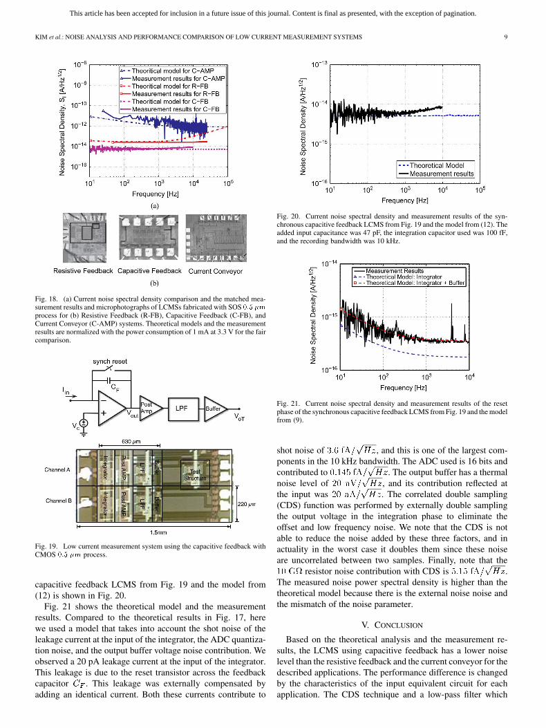
and at the maximum band-width frequency of 10 kHz, respectively. However, the analysisof capacitive feedback system shows the noise spectral densityof . From the measurement results, we seethe measured RMS noise of the capacitive feedback system is110 fA RMS (calculated) and 750 fA RMS (measured) at a10 kHz sampling rate, whereas the measured RMS noises of the
resistive feedback and the current conveyor are 4 pA and 600 pAwith a bandwidth of 10 kHz, respectively. Since the dominantnoise source of the resistive feedback is the thermal noise of thefeedback resistor, the measured results matched well with thenoise analysis. However, the measured RMS noises are slightlyhigher than the theoretical analysis values due to the signal de-pendent switching effect and the mismatch of noise parametersin the cases of the capacitive feedback and current conveyor sys-tems. Nevertheless, the noise analysis presented here gives verygood matching results.
Recently, we have fabricated an optimized synchronousLCMS with capacitive feedback based on the noise analysiscomparison reported in this paper. The optimized LCMS usingcapacitive feedback was designed and fabricated in a CMOS
process, since the SOS process has higher low fre-quency noise (flicker noise) than the CMOS process. The circuitand layout of this system are shown in Fig. 19. The fabricatedLCMS has two channels, a selectable 100 fF or 1 pF feedbackcapacitor, and each channel occupies . TheLCMS noise performance was tested using precisely knowncurrents by applying voltage over a resistor using aKeithley 236 Source Measure Unit. For this test we used a100 fF integration cap, a 10 kHz sampling rate, and we didnot filter the output voltage (worst case scenario). The inputcapacitance of the system packaged in a circuit board and withthe resistor was estimated to be 8 pF. The current noisespectral density and measurement results of the synchronous
This article has been accepted for inclusion in a future issue of this journal. Content is final as presented, with the exception of pagination.
KIM et al.: NOISE ANALYSIS AND PERFORMANCE COMPARISON OF LOW CURRENT MEASUREMENT SYSTEMS 9
Fig. 18. (a) Current noise spectral density comparison and the matched mea-surement results and microphotographs of LCMSs fabricated with SOS �����process for (b) Resistive Feedback (R-FB), Capacitive Feedback (C-FB), andCurrent Conveyor (C-AMP) systems. Theoretical models and the measurementresults are normalized with the power consumption of 1 mA at 3.3 V for the faircomparison.
Fig. 19. Low current measurement system using the capacitive feedback withCMOS ��� �� process.
capacitive feedback LCMS from Fig. 19 and the model from(12) is shown in Fig. 20.
Fig. 21 shows the theoretical model and the measurementresults. Compared to the theoretical results in Fig. 17, herewe used a model that takes into account the shot noise of theleakage current at the input of the integrator, the ADC quantiza-tion noise, and the output buffer voltage noise contribution. Weobserved a 20 pA leakage current at the input of the integrator.This leakage is due to the reset transistor across the feedbackcapacitor . This leakage was externally compensated byadding an identical current. Both these currents contribute to
Fig. 20. Current noise spectral density and measurement results of the syn-chronous capacitive feedback LCMS from Fig. 19 and the model from (12). Theadded input capacitance was 47 pF, the integration capacitor used was 100 fF,and the recording bandwidth was 10 kHz.
Fig. 21. Current noise spectral density and measurement results of the resetphase of the synchronous capacitive feedback LCMS from Fig. 19 and the modelfrom (9).
shot noise of , and this is one of the largest com-ponents in the 10 kHz bandwidth. The ADC used is 16 bits andcontributed to . The output buffer has a thermalnoise level of , and its contribution reflected atthe input was . The correlated double sampling(CDS) function was performed by externally double samplingthe output voltage in the integration phase to eliminate theoffset and low frequency noise. We note that the CDS is notable to reduce the noise added by these three factors, and inactuality in the worst case it doubles them since these noiseare uncorrelated between two samples. Finally, note that the
resistor noise contribution with CDS is .The measured noise power spectral density is higher than thetheoretical model because there is the external noise noise andthe mismatch of the noise parameter.
V. CONCLUSION
Based on the theoretical analysis and the measurement re-sults, the LCMS using capacitive feedback has a lower noiselevel than the resistive feedback and the current conveyor for thedescribed applications. The performance difference is changedby the characteristics of the input equivalent circuit for eachapplication. The CDS technique and a low-pass filter which

This article has been accepted for inclusion in a future issue of this journal. Content is final as presented, with the exception of pagination.
10 IEEE TRANSACTIONS ON BIOMEDICAL CIRCUITS AND SYSTEMS
has a bandwidth which can be changed depending on the inputsignal frequency can increase the noise performance of the syn-chronous capacitive feedback LCMS. This paper also presentsa comprehensive analysis of low-current measurement systemsand helps technical personnel, scientists and engineers to designthe lowest noise system for biomedical and nano-science appli-cations.
REFERENCES
[1] F. Sigworth and K. Klemic, “Microchip technology in ion-channel re-search,” IEEE Trans. Nanobiosci., vol. 4, pp. 121–127, 2005.
[2] D. Branton et al., “The potential and challenges of nanopore se-quencing,” Nature Biotechnol., vol. 26, pp. 1146–1153, 2008.
[3] E. Katz and I. Willner, “Probing biomolecular interactions at con-ductive and semiconductive surfaces by impedance spectroscopy:Routes to impedimetric immunosensors, dna-sensors, and enzymebiosensors,” Electroanal., vol. 15, no. 11, pp. 913–947, 2003.
[4] E. Stern, J. Klemic, D. Routenberg, P. Wyrembak, D. Turner-Evans, A.Hamilton, D. LaVan, T. Fahmy, and M. Reed, “Label-free immunode-tection with CMOS-compatible semiconducting nanowires,” Nature,vol. 05498, no. 445, 2007.
[5] R. J. Reay, S. P. Kounaves, and G. T. Kovacs, “An integrated CMOSpotentiostat for miniaturized electroanalytical instrumentation,” inProc. IEEE Int. Solid-State Circuits Conf., Feb. 1994, pp. 162–163.
[6] K. Murari, N. Thakor, M. Stanacevic, and G. Cauwenberghs,“Wide-range, picoampere-sensitivity multichannel VLSI potentiostatfor neurotransmitter sensing,” in Proc. 26th Annu. Int. Conf. IEEEEngineering in Medicine and Biology Society, San Francisco, CA,Sep. 2004.
[7] R. Genov, M. Stanacevic, M. Naware, G. Cauwenberghs, and N.Thakor, “16-channel integrated potentiostat for distributed neuro-chemical sensing,” IEEE Trans. Circuits Syst. I, Reg. Papers, vol. 53,no. 11, pp. 2371–2376, 2006.
[8] A. Gore, S. Chakrabartty, and E. Alocilja, “A multichannel femtoam-pere-sensitivity potentiostat array for biosensing applications,” IEEETrans. Circuits Syst. I, Reg. Papers, vol. 53, no. 11, pp. 2357–2363,2006.
[9] G. Ferrari, F. Gozzini, and M. Sampietro, “Very high sensitivity CMOScircuit to track fast biological current signals,” in Proc. IEEE Biomed-ical Circuits and Systems Conf., 2006, pp. 53–56.
[10] G. Ferrari, F. Gozzini, and M. Sampietro, “A current-sensitivefront-end amplifier for nano-biosensors with a 2 MHz BW,” in Proc.IEEE Int. Solid-State Circuits Conf., Dig. Tech. Papers, 2007, pp.164–165.
[11] M. Stanacevic, K. Murari, A. Rege, G. Cauwenberghs, and N. Thakor,“VLSI potentiostat array with oversampling gain modulation for wide-range neurotransmitter sensing,” IEEE Trans. Biomed. Circuits Syst.,vol. 1, no. 1, pp. 63–72, 2007.
[12] A. Yang, S. R. Jadhav, R. M. Worden, and A. J. Mason, “Compact low-power impedance-to-digital converter for sensor array microsystems,”IEEE J. Solid-State Circuits, vol. 44, no. 10, pp. 2844–2855, 2009.
[13] G. Ferrari, F. Gozzini, A. Molari, and M. Sampietro, “Transimpedanceamplifier for high sensitivity current measurements on nanodevices,”IEEE J. Solid-State Circuits, vol. 44, no. 5, pp. 1609–1616, May 2009.
[14] E. Culurciello, Silicon-on-Sapphire Circuits and Systems, Sensor andBiosensor Interfaces. New York: McGraw-Hill, 2009.
[15] G. Ferrari, M. Farina, F. Guagliardo, M. Carminati, and M. Sampietro,“Ultra-low-noise CMOS current preamplifier from dc to 1 MHz,” Elec-tron. Lett., vol. 45, p. 1278, 2009.
[16] D. Kim, W. Tang, B. Goldstein, P. Weerakoon, and E. Culurciello,“Performance comparison of low current measurement systems forbiomedical applications,” in Proc. IEEE Int. Symp. Circuits andSystems, Paris, France, May 2010.
[17] B. Razavi, Design of Analog CMOS Integrated Circuits. New York:McGraw-Hill, 2000.
[18] A. Hassibi, R. Navid, R. Dutton, and T. Lee, “Comprehensive study ofnoise processes in electrode electrolyte interfaces,” J. Appl. Phys., vol.96, p. 1074, 2004.
[19] A. Hassibi, H. Vikalo, and A. Hajimiri, “On noise processes andlimits of performance in biosensors,” J. Appl. Phys., vol. 102, no. 1, p.014909, 2007.
[20] O. Hamill, A. Marty, E. Neher, B. Sakmann, and F. Sigworth, “Im-proved patch-clamp technique for high-resolution current recordingfrom cells and cell-free membrane patches,” Eur. J. Phys., vol. 391,pp. 85–100, 1981.
[21] R. Levi and J. Rae, “Technology of patch-clamp electrodes,” Patch-Clamp Anal., pp. 1–34, 2007.
[22] N. Fertig, R. Blick, and J. Behrends, “Whole cell patch clamprecording performed on a planar glass chip,” Biophys. J., vol. 82, no.6, pp. 3056–3062, 2002.
[23] S. M. Iqbal, Nanopores: Sensing and Fundamental Biological Interac-tions. Berlin, Germany: Springer, 2011.
[24] P. Weerakoon, E. Culurciello, Y. Yang, J. Santos-Sacchi, P. Kindl-mann, and F. Sigworth, “Patch-clamp amplifiers on a chip,” J. Neu-rosci. Methods, vol. 192, pp. 187–192, Oct. 2010.
[25] P. Weerakoon, F. Sigworth, P. Kindlmann, J. Santos-Sacchi, Y. Yang,and E. Culurciello, “An integrated patch-clamp system with dualinput,” in Proc. IEEE Int. Symp. Circuits and Systems, Paris, France,May 2010.
[26] P. Weerakoon, K. Klemic, F. Sigworth, and E. Culurciello, “An inte-grated patch-clamp potentiostat with electrode compensation,” IEEETrans. Biomed. Circuits Syst., vol. 3, no. 2, pp. 117–125, 2009.
[27] P. Weerakoon, K. Klemic, F. Sigworth, and E. Culurciello, “Integratedpatch-clamp biosensor for high-density screening of cell conductance,”Electron. Lett., vol. 44, no. 2, pp. 81–82, Jan. 2008.
[28] R. G. Kakerow, H. Kappert, E. Spiegel, and Y. Manoli, “Low powersingle chip CMOS potentiostat,” in Proc. 8th Int. Conf. Solid-State Sen-sors and Actuators, Jun. 1995, pp. 142–145.
[29] A. Bandyopadhyay, G. Mulliken, G. Cauwenberghs, and N. Thakor,“VLSI potentiostat array for distributed electrochemical neuralrecording,” in Proc. IEEE Int. Symp. Circuits and Systems, Phoenix,AZ, May 2002, pp. II-740–II-743.
[30] H. Narula and J. Harris, “A time-based vlsi potentiostat for ion currentmeasurements,” IEEE Sensors J., vol. 6, no. 2, pp. 239–247, Apr. 2006.
[31] R. Bracewell, “The Fourier transform,” Sci. Amer., vol. 260, no. 6, pp.86–95, 1989.
[32] R. F. Turner, D. J. Harrison, and H. P. Baltes, “A CMOS potentiostatfor amperometric chemical sensors,” IEEE J. Solid State Circuits, vol.22, pp. 473–478, May 1987.
[33] E. Bruun, “Analysis of the noise characteristics of cmos current con-veyors,” Analog Integr. Circuits Signal Process., vol. 12, no. 1, pp.71–78, Jan. 1997.
[34] F. Laiwalla, K. Klemic, F. Sigworth, and E. Culurciello, “An inte-grated patch-clamp amplifier in silicon-on-Sapphire CMOS,” IEEETrans. Circuits Syst., vol. 53, no. 11, pp. 2364–2370, Nov. 2006.
[35] F. Laiwalla, K. Klemic, F. Sigworth, and E. Culurciello, “An integratedsilicon-on-sapphire patch-clamp amplifier,” in Proc. IEEE/NLM LifeScience Systems and Application Workshop, Bethesda, MD, Jul. 2006.
[36] F. Laiwalla, K. Klemic, F. Sigworth, and E. Culurciello, “An inte-grated patch-clamp amplifier in silicon-on-sapphire CMOS,” in Proc.IEEE Int. Symp. Circuits and Systems, Kos, Greece, May 2006, pp.4054–4057.
[37] E. Culurciello, H. Montanaro, and D. Kim, “Ultra-low current mea-surements with silicon-on-sapphire integrator circuits,” IEEE ElectronDevice Lett., vol. 30, no. 3, pp. 258–260, Mar. 2009.
Dongsoo Kim (M’02) received the M.S. and Ph.D.degrees in electrical and electronics engineering fromYonsei University, Seoul, Korea, in 2004 and 2008,respectively
Currently, he works as a Senior Analog DesignEngineer at Aptina Imaging, San Jose, CA. From2008 to 2010, he was a Postdoctoral Associate in theDepartment of Electrical Engineering, Yale Univer-sity, New Haven, CT. His research interests includeCMOS image sensors, smart sensors, low-noisecircuit design, and biomedical instrumentation.
This article has been accepted for inclusion in a future issue of this journal. Content is final as presented, with the exception of pagination.
KIM et al.: NOISE ANALYSIS AND PERFORMANCE COMPARISON OF LOW CURRENT MEASUREMENT SYSTEMS 11
Brian Goldstein (GS’08) received the B.S. degreein computer and systems engineering and computerscience from Rensselaer Polytechnic Institute, Troy,NY, in 2006, and the M.S. and M.Phil. degrees inelectrical engineering from Yale University, NewHaven, CT, in 2010 and 2011, respectively.
Currently, he is working toward the Ph.D. degreeat Yale University. From 2006 to 2008, he workedon embedded systems at Goodrich Pump and EngineControl Systems, N.A., West Hartford, CT. His re-search interests include analog and mixed-signal in-
tegrated circuits, low-noise circuit design, and systems engineering for biomed-ical applications.
Wei Tang (S’06) received the B.S. degree in micro-electronics from Peking University, Peking, China, in2006.
Currently, he is working toward the Ph.D. degree atYale University, New Haven, CT. In 2007, he becamea Research Assistant in the Yale E-Lab. His researchinterests are analog/mixed-signal and low-power cir-cuit design, as well as RF/wireless communicationcircuits and systems design and testing for biomed-ical applications.
Fred J. Sigworth received the B.S. degree in appliedphysics from the California Institute of Technology,Pasadena, in 1974, and the Ph.D. degree in physi-ology from Yale University, New Haven, CT, in 1979.
He has worked in the laboratory of C. F. Stevensat Yale University. He was a Postdoctoral Fellow inthe laboratory of E. Neher in Göttingen, Germany.Since 1984, he has been a Faculty Member in the De-partment of Cellular and Molecular Physiology at theYale School of Medicine, and holds a joint appoint-ment in the Department of Biomedical Engineering.
His research group studies the function and structure of ion-channel proteins.
Eugenio Culurciello (S’97–M’99–SM’11) re-ceived the Ph.D. degree in electrical and computerengineering from The Johns Hopkins University,Baltimore, MD, in 2004.
He is an Associate Professor in the Weldon Schoolof Biomedical Engineering, Purdue University, WestLafayette, IN, where he directs the e-Lab laboratory.His research interests include analog and mixedmodeintegrated circuits for biomedical instrumentation,synthetic vision, bio-inspired sensory systems andnetworks, biological sensors, and silicon-on-insu-
lator design. He was the recipient of The Presidential Early Career Award forScientists and Engineers (PECASE) and Young Investigator Program fromONR, the Distinguished Lecturer of the IEEE (CASS), and is the author ofSilicon-on-Sapphire Circuits and Systems, Sensor and Biosensor Interfaces(McGraw-Hill: New York) in 2009.