ieee transactions on biomedical circuits and...
TRANSCRIPT
IEEE TRANSACTIONS ON BIOMEDICAL CIRCUITS AND SYSTEMS, VOL. 2, NO. 3, SEPTEMBER 2008 231
An Integrated Implantable Stimulator That isFail-Safe Without Off-Chip Blocking-Capacitors
Xiao Liu, Student Member, IEEE, Andreas Demosthenous, Senior Member, IEEE, and Nick Donaldson
Abstract—We present a neural stimulator chip with an outputstage (electrode driving circuit) that is fail-safe under single-faultconditions without the need for off-chip blocking-capacitors. Tominiaturize the stimulator output stage two novel techniquesare introduced. The first technique is a new current generatorcircuit reducing to a single step the translation of the digital inputbits into the stimulus current, thus minimizing silicon area andpower consumption compared to previous works. The currentgenerator uses voltage-controlled resistors implemented by MOStransistors in the deep triode region. The second technique is anew stimulator output stage circuit with blocking-capacitor safetyprotection using a high-frequency current-switching (HFCS)technique. Unlike conventional stimulator output stage circuitsfor implantable functional electrical stimulation (FES) systemswhich require blocking-capacitors in the microfarad range, ourproposed approach allows capacitance reduction to the picofaradrange, thus the blocking-capacitors can be integrated on-chip.The prototype four-channel neural stimulator chip was fabricatedin XFAB’s 1- m silicon-on-insulator CMOS technology and canoperate from a power supply between 5–18 V. The stimulus cur-rent is generated by active charging and passive discharging. Weobtained recordings of action potentials and a strength-durationcurve from the sciatic nerve of a frog with the stimulator chipwhich demonstrate the HFCS technique. The average powerconsumption for a typical 1-mA 20-Hz single-channel stimulationusing a book electrode, is 200 W from a 6 V power supply. Thesilicon area occupation is 0.38 mm� per channel.
Index Terms—Action potential, biomedical circuits, blocking-ca-pacitor, capacitance reduction, current generator, fail-safe, func-tional electrical stimulation (FES), implanted device, neural stim-ulator.
I. INTRODUCTION
F OR a patient suffering from spinal cord injury, the normaldirect control of the lower limbs by the brain is lost.
However, most of the nerves and muscles below the injury arenot affected and can be used if artificially stimulated by meansof functional electrical stimulation (FES) [1]. For example, ithas been demonstrated that leg muscle function [2], [3] andbladder-emptying [4] can be restored by applying trains of
Manuscript received June 24, 2008; revised January 22, 2008 and April 09,2008. Current version published October 24, 2008. This work was funded bythe European Commission under IMANE project IST-026602. This paper wasrecommended by Associate Editor K. Chakrabarty.
X. Liu and A. Demosthenous are with the Electrical and Electronic Engi-neering Department, University College London, London, WC1E 7JE U.K.(e-mail: [email protected], [email protected]).
N. Donaldson is with the Department of Medical Physics and Bioengineering,University College London, Malet Place, London WC1E 6BT, U.K. (e-mail:[email protected]).
Color versions of one or more of the figures in this paper are available onlineat http://ieeexplore.ieee.org.
Digital Object Identifier 10.1109/TBCAS.2008.2003199
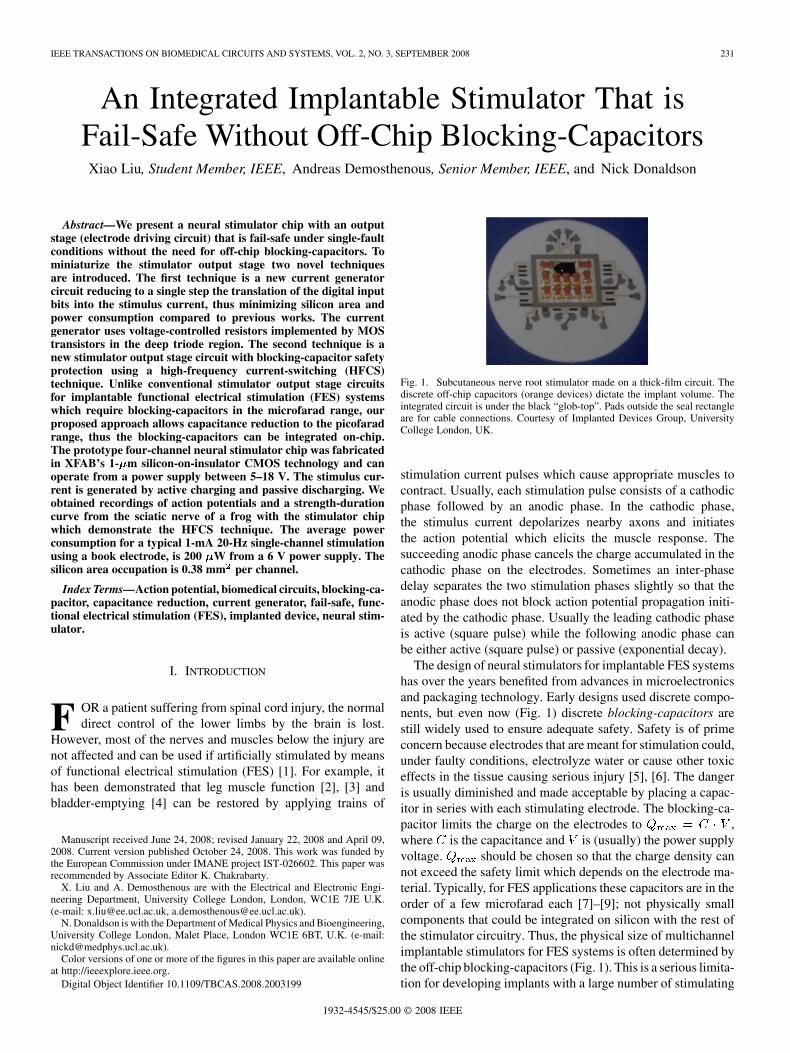
Fig. 1. Subcutaneous nerve root stimulator made on a thick-film circuit. Thediscrete off-chip capacitors (orange devices) dictate the implant volume. Theintegrated circuit is under the black “glob-top”. Pads outside the seal rectangleare for cable connections. Courtesy of Implanted Devices Group, UniversityCollege London, UK.
stimulation current pulses which cause appropriate muscles tocontract. Usually, each stimulation pulse consists of a cathodicphase followed by an anodic phase. In the cathodic phase,the stimulus current depolarizes nearby axons and initiatesthe action potential which elicits the muscle response. Thesucceeding anodic phase cancels the charge accumulated in thecathodic phase on the electrodes. Sometimes an inter-phasedelay separates the two stimulation phases slightly so that theanodic phase does not block action potential propagation initi-ated by the cathodic phase. Usually the leading cathodic phaseis active (square pulse) while the following anodic phase canbe either active (square pulse) or passive (exponential decay).
The design of neural stimulators for implantable FES systemshas over the years benefited from advances in microelectronicsand packaging technology. Early designs used discrete compo-nents, but even now (Fig. 1) discrete blocking-capacitors arestill widely used to ensure adequate safety. Safety is of primeconcern because electrodes that are meant for stimulation could,under faulty conditions, electrolyze water or cause other toxiceffects in the tissue causing serious injury [5], [6]. The dangeris usually diminished and made acceptable by placing a capac-itor in series with each stimulating electrode. The blocking-ca-pacitor limits the charge on the electrodes to ,where is the capacitance and is (usually) the power supplyvoltage. should be chosen so that the charge density cannot exceed the safety limit which depends on the electrode ma-terial. Typically, for FES applications these capacitors are in theorder of a few microfarad each [7]–[9]; not physically smallcomponents that could be integrated on silicon with the rest ofthe stimulator circuitry. Thus, the physical size of multichannelimplantable stimulators for FES systems is often determined bythe off-chip blocking-capacitors (Fig. 1). This is a serious limita-tion for developing implants with a large number of stimulating
1932-4545/$25.00 © 2008 IEEE
232 IEEE TRANSACTIONS ON BIOMEDICAL CIRCUITS AND SYSTEMS, VOL. 2, NO. 3, SEPTEMBER 2008
channels for finer interaction with the nervous system. Suchstimulators would allow selective stimulation of smaller nervefibre groups in, for example, the lower motor nerves, whichcould lead to more natural control of movement of paralyzedmuscles [10].
Apart from protection against electrolysis following semicon-ductor failure, the use of blocking-capacitors provides a simplesolution to maintaining charge-balance during normal stimu-lation [11], [12]. However, this can also be achieved by re-lying on the capacitive property of polarizable electrodes suchas porous platinum (Pt) or iridium oxide [13]–[15] with pas-sive discharging. This method is utilized in the stimulator outputstage circuit presented in this paper. A recent paper has reporteda blocking-capacitor-free stimulator that achieves very precisecharge-balanced active biphasic stimulation implemented in astandard CMOS technology [16]. However, unlike the stimu-lator chip described in this paper, the stimulator chip in [16]cannot be guaranteed fail-safe under single-fault conditions.
There are other methods of protection that do not utilizeblocking-capacitors, including continuous monitoring of theelectrode-tissue impedance [17], [18], the stimulus current level[19] or the electrode voltage [20], [21]. The recorded valuesare continuously compared with a predefined reference, whichwhen exceeded, inhibits the stimulator output stage to preventnerve damage. The advantage of this approach is volumesaving because the monitoring circuit can be integrated withthe stimulator output stage circuit. However, the monitoringcircuit increases the stimulator output stage complexity, whichitself increases the likelihood of semiconductor failure.
It should be noted that electrostatic discharge (ESD) protec-tion at all I/O pads of the stimulator chip is an important require-ment for safe handling and is especially necessary for the padsconnecting to the stimulating electrodes. Usually, the standardI/O pads from the technology provider can be used, as was thecase for the stimulator chip in this paper. However, for appli-cations requiring many stimulating channels, e.g., retinal pros-thesis, the area of the standard I/O pads may be too large tomeet the constraints of the available physical space. A compactcustom-made ESD cell can be found in [21].
In this paper, we present a neural stimulator with an outputstage (electrode driving circuit) that is fail-safe under single-fault conditions without the need for off-chip blocking-capac-itors. In order to miniaturize the stimulator output stage twonovel techniques are introduced. The first technique is a newcurrent generator circuit that reduces to a single step the trans-lation of the digital input bits into the stimulus current, thusminimizing silicon area and power consumption compared toprevious works. The current generator uses voltage-controlledMOS resistors in the deep triode region and features high lin-earity, small voltage compliance1 and high output impedance.It is also more compact than previous current generator circuitsused in implantable neural stimulators and its linearity perfor-mance is not affected by mobility reduction. The second tech-nique is a new stimulator output stage circuit with blocking-ca-pacitor safety protection that utilizes our high-frequency cur-
1We define voltage compliance as the minimum output voltage at which thecurrent generator still provides a high output resistance [22].
rent-switching (HFCS) technique [23], [24] and passive dis-charging. Unlike conventional stimulator output stage circuitsfor implantable FES systems which require blocking-capacitorsin the microfarad range, our proposed approach enables capac-itance reduction to the picofarad range pF . Hence, thecomplete stimulator can be integrated on a single silicon chipand still be fail-safe. The prototype four-channel neural stimu-lator chip was fabricated in XFAB’s 1- m silicon-on-insulator(SOI) CMOS technology. We obtained successful recordings ofaction potentials and a strength-duration curve from the sciaticnerve of a frog with our stimulator which demonstrate the prac-ticality of stimulating real nerve by the HFCS technique.
The remaining sections of the paper are organized as follows.Section II describes three conventional stimulator output stagecircuits with blocking-capacitors and presents an overview ofprevious work on the design of current generator circuits forimplantable neural stimulation. Section III describes the newcurrent generator circuit (for a 4-bit implementation) and Sec-tion IV explains the HFCS technique and presents the new stim-ulator output stage circuit. The architecture of the fabricatedstimulator including measured results and the in vitro experi-ments are presented in Section V. Finally, Section VI concludesthe paper by summarizing our contributions.
II. OVERVIEW OF STIMULATOR OUTPUT STAGE DESIGNS AND
CURRENT GENERATOR CIRCUITS
A. Stimulator Output Stages Utilizing Blocking-Capacitors
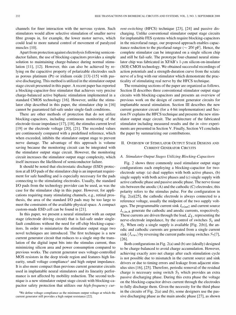
Fig. 2 shows three commonly used stimulator output stageconfigurations each employing a blocking-capacitor for two-electrode setup: (a) dual supplies with both active phases, (b)single supply with both active phases and (c) single supply withactive cathodic phase and passive anodic phase. The nerve tissuesits between the anodic (A) and the cathodic (C) electrodes; thispolarity refers to the stimulus pulse. For the configuration inFig. 2(a)[25], the cathodic electrode is always connected to areference voltage, usually the midpoint of the two supply volt-ages. The programmable current sink and current source
generate the cathodic and anodic currents, respectively.These currents are driven through the load, , representing thenerve-electrode impedance, by the control of switches and
. When only a single supply is available [Fig. 2(b)], the an-odic and cathodic currents are generated from a single currentsink by reversing the current paths using switches [7],[26].
Both configurations in Fig. 2(a) and (b) are (ideally) designedto be charge-balanced to avoid charge accumulation. However,achieving exactly zero net charge after each stimulation cycleis not possible due to mismatch in the current source and sinkdrivers or due to timing errors and leakage from adjacent stim-ulus sites [16], [25]. Therefore, periodic removal of the residualcharge is necessary using switch which provides an extrapassive discharging phase. During this extra phase the voltageon the blocking-capacitor drives current through the electrodesto fully discharge them. Given the necessity for the third phasein the circuits of Fig. 2(a) and (b), some designers use the pas-sive discharging phase as the main anodic phase [27], as shown
LIU et al.: AN INTEGRATED IMPLANTABLE STIMULATOR THAT IS FAIL-SAFE WITHOUT OFF-CHIP BLOCKING-CAPACITORS 233
Fig. 2. Conventional stimulator output stage configurations for two-electrode setup. (a) Dual supplies with active cathodic and active anodic phases. (b) Singesupply with active cathodic and active anodic phases. (c) Single supply with active cathodic phase and passive anodic phase.
in the circuit of Fig. 2(c). Passive discharging is easily imple-mented but the discharging phase must be long enough.
As mentioned in Section I, the voltage on the electrode capac-itance can also drive the passive discharging current. However,blocking-capacitors may still be considered necessary to en-sure that direct current cannot flow if the electrodes are chargedbeyond their capacitive range (“water window”) due to semi-conductor or other fault. Various mechanisms of semiconductorfailure in stimulators either implanted or under accelerated testshave been reported. These include short-circuit due to mois-ture penetration into the glass seal of the silicon package [28],[29], gate-oxide breakdown [30] and change of device param-eters after implantation, for example, due to ionizing radiation[31].
B. Current Generator Circuits
Several current generator circuits for implantable neural stim-ulators have been reported in the literature. The full-scale outputcurrent varies from about 100 A to 16 mA and the resolutionfrom 3 to 8 bits, depending on the application. Desirable fea-tures for a current generator circuit for use in this applicationare small voltage compliance, high output impedance, good lin-earity, low power consumption and small silicon area.
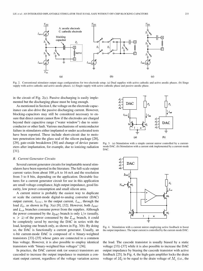
A current mirror is probably the easiest way to duplicateor scale the current-mode digital-to-analog converter (DAC)output current, , to the output current, , through theload , as shown in Fig. 3(a) [9], [32]. However, bothand branches consume power from the supplies. Althoughthe power consumed by the branch is only (usually,
) of the power consumed by the branch, it couldbe completely saved by moving the DAC in series with theload, keeping one branch only, as shown in Fig. 3(b). By doingso, the DAC is functionally a current generator. Usually, an
-bit current-mode DAC is composed of binary-weightedtransistors [33]–[35] whose gates are connected to a commonbias voltage. However, it is also possible to employ identicaltransistors with “binary-weighted bias voltages” [36].
In practice, the DAC current sink (or source) transistors arecascoded to increase the output impedance to maintain a con-stant output current, regardless of the voltage variation across
Fig. 3. (a) Stimulation with a simple current mirror controlled by a current-mode DAC. (b) Stimulation with a current sink implemented by a current-modeDAC.
Fig. 4. Stimulation with a current mirror employing active feedback to boostthe output impedance. The input current is controlled by the current-mode DAC.
the load. The cascode transistor is usually biased by a staticvoltage [33]–[37] while it is also possible to increase the DACoutput impedance by biasing the cascode transistor with activefeedback [25]. In Fig. 4, the high-gain amplifier locks the drainvoltage of to be equal to the drain voltage of (i.e., the
234 IEEE TRANSACTIONS ON BIOMEDICAL CIRCUITS AND SYSTEMS, VOL. 2, NO. 3, SEPTEMBER 2008
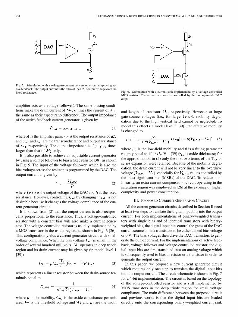
Fig. 5. Stimulation with a voltage-to-current conversion circuit employing ac-tive feedback. The output current is the ratio of the DAC output voltage over thefixed resistance.
amplifier acts as a voltage follower). The same biasing condi-tions make the drain current of , times the current of ,the same as their aspect ratio difference. The output impedanceof the active feedback current generator is given by
(1)
where is the amplifier gain, is the output resistance ofand and are the transconductance and output resistanceof , respectively. The output impedance is timeslarger than that of only.
It is also possible to achieve an adjustable current generatorby using a voltage follower to bias a fixed resistor [38], as shownin Fig. 5. The input of the voltage follower, which is also thebias voltage across the resistor, is programmed by the DAC. Theoutput current is given by
(2)
where is the output voltage of the DAC and is the fixedresistance. However, controlling by changing is notdesirable because it changes the voltage compliance of the cur-rent generator circuit.
It is known from (2) that the output current is also recipro-cally proportional to the resistance. Thus, a voltage-controlledresistor with a constant bias will also make a current gener-ator. The voltage-controlled resistor is usually implemented bya MOS transistor in the triode region, as shown in Fig. 6 [26].This configuration yields a current generator circuit with smallvoltage compliance. When the bias voltage is small, in theorder of several hundred millivolts, operates in deep trioderegion and its drain current may be given by (in model level 1[39])
(3)
which represents a linear resistor between the drain-source ter-minals equal to
(4)
where is the mobility, is the oxide capacitance per unitarea, is the threshold voltage and and are the width
Fig. 6. Stimulation with a current sink implemented by a voltage-controlledMOS resistor. The active resistance is controlled by the voltage-mode DACoutput.
and length of transistor , respectively. However, at largegate-source voltages (i.e., for large ), mobility degra-dation due to the high vertical field cannot be neglected. Tomodel this effect (in model level 3 [39]), the effective mobilityis changed to
(5)
where is the low-field mobility and is a fitting parameterroughly equal to V [39] ( is oxide thickness); forthe approximation in (5) only the first two terms of the Taylorseries expansion were retained. Because of the mobility degra-dation, the drain current will not be very linear to the overdrivevoltage , especially for values controlled bythe most significant bits (MSBs) of the DAC. To reduce non-linearity, an extra current compensation circuit operating in thesaturation region was employed in [26] at the expense of highercomplexity and power consumption.
III. PROPOSED CURRENT GENERATOR CIRCUIT
All the current generator circuits described in Section II needat least two steps to translate the digital input bits into the outputcurrent. For both implementations of binary-weighted transis-tors with single bias and of identical transistors with binary-weighted bias, the digital input bits control the gates of the DACcurrent source or sink transistors to be either a fixed bias voltageor 0 V. The bias voltages then drive the DAC transistors to gen-erate the output current. For the implementations of active feed-back, voltage follower and voltage-controlled resistor, the dig-ital input bits are first translated into an analog voltage whichis subsequently used to bias a resistor or a transistor in order togenerate the output current.
In this paper, we propose a new current generator circuitwhich requires only one step to translate the digital input bitsinto the output current. The circuit schematic is shown in Fig. 7for a 4-bit implementation. The circuit is based on the topologyof the voltage-controlled resistor and is still implemented byMOS transistors in the deep triode region for small voltagecompliance. The main difference between the proposed circuitand previous works is that the digital input bits are loadeddirectly onto the corresponding binary-weighted current sink
LIU et al.: AN INTEGRATED IMPLANTABLE STIMULATOR THAT IS FAIL-SAFE WITHOUT OFF-CHIP BLOCKING-CAPACITORS 235
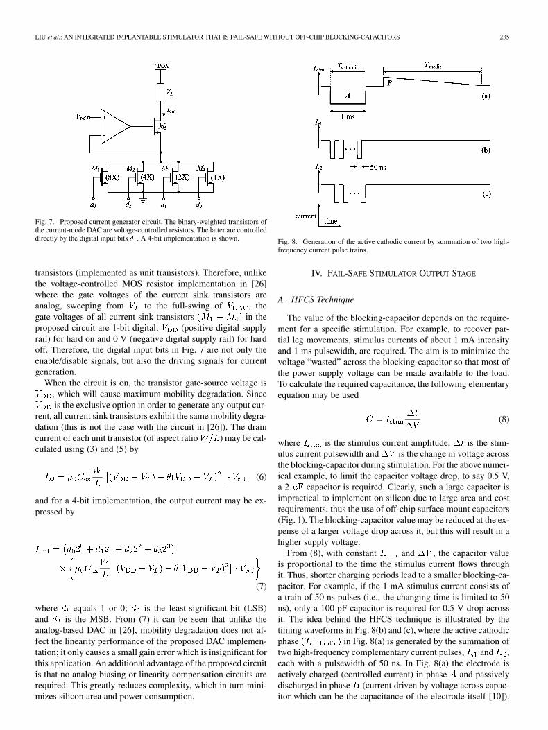
Fig. 7. Proposed current generator circuit. The binary-weighted transistors ofthe current-mode DAC are voltage-controlled resistors. The latter are controlleddirectly by the digital input bits � . A 4-bit implementation is shown.
transistors (implemented as unit transistors). Therefore, unlikethe voltage-controlled MOS resistor implementation in [26]where the gate voltages of the current sink transistors areanalog, sweeping from to the full-swing of , thegate voltages of all current sink transistors in theproposed circuit are 1-bit digital; (positive digital supplyrail) for hard on and 0 V (negative digital supply rail) for hardoff. Therefore, the digital input bits in Fig. 7 are not only theenable/disable signals, but also the driving signals for currentgeneration.
When the circuit is on, the transistor gate-source voltage is, which will cause maximum mobility degradation. Sinceis the exclusive option in order to generate any output cur-
rent, all current sink transistors exhibit the same mobility degra-dation (this is not the case with the circuit in [26]). The draincurrent of each unit transistor (of aspect ratio ) may be cal-culated using (3) and (5) by
(6)
and for a 4-bit implementation, the output current may be ex-pressed by
(7)
where equals 1 or 0; is the least-significant-bit (LSB)and is the MSB. From (7) it can be seen that unlike theanalog-based DAC in [26], mobility degradation does not af-fect the linearity performance of the proposed DAC implemen-tation; it only causes a small gain error which is insignificant forthis application. An additional advantage of the proposed circuitis that no analog biasing or linearity compensation circuits arerequired. This greatly reduces complexity, which in turn mini-mizes silicon area and power consumption.
Fig. 8. Generation of the active cathodic current by summation of two high-frequency current pulse trains.
IV. FAIL-SAFE STIMULATOR OUTPUT STAGE
A. HFCS Technique
The value of the blocking-capacitor depends on the require-ment for a specific stimulation. For example, to recover par-tial leg movements, stimulus currents of about 1 mA intensityand 1 ms pulsewidth, are required. The aim is to minimize thevoltage “wasted” across the blocking-capacitor so that most ofthe power supply voltage can be made available to the load.To calculate the required capacitance, the following elementaryequation may be used
(8)
where is the stimulus current amplitude, is the stim-ulus current pulsewidth and is the change in voltage acrossthe blocking-capacitor during stimulation. For the above numer-ical example, to limit the capacitor voltage drop, to say 0.5 V,a 2 capacitor is required. Clearly, such a large capacitor isimpractical to implement on silicon due to large area and costrequirements, thus the use of off-chip surface mount capacitors(Fig. 1). The blocking-capacitor value may be reduced at the ex-pense of a larger voltage drop across it, but this will result in ahigher supply voltage.
From (8), with constant and , the capacitor valueis proportional to the time the stimulus current flows throughit. Thus, shorter charging periods lead to a smaller blocking-ca-pacitor. For example, if the 1 mA stimulus current consists ofa train of 50 ns pulses (i.e., the changing time is limited to 50ns), only a 100 pF capacitor is required for 0.5 V drop acrossit. The idea behind the HFCS technique is illustrated by thetiming waveforms in Fig. 8(b) and (c), where the active cathodicphase in Fig. 8(a) is generated by the summation oftwo high-frequency complementary current pulses, and ,each with a pulsewidth of 50 ns. In Fig. 8(a) the electrode isactively charged (controlled current) in phase and passivelydischarged in phase (current driven by voltage across capac-itor which can be the capacitance of the electrode itself [10]).

236 IEEE TRANSACTIONS ON BIOMEDICAL CIRCUITS AND SYSTEMS, VOL. 2, NO. 3, SEPTEMBER 2008
Fig. 9. (a) Proposed stimulator output stage utilizing the HFCS technique andpassive discharge. (b) Timing waveforms.
For charge-balance, the areas under and must be equal andthis is achieved by making the passive anodic phasemuch longer than .
B. Proposed Output Stage
Fig. 9 shows the simplified schematic of the proposedstimulator output stage circuit utilizing HFCS and passivedischarging. The circuit uses two small blocking-capacitors( and ), one for the current branch and the other for the
current branch. The timing waveforms in the same figurecontrol switches and .
The operation of the circuit is as follows. During clock phase, for the branch, is closed and is open. The load
switch is also open. In this phase, diode is reverse-bi-ased and diode is forward-biased. The constant current(generated by the programmable current generator circuit inFig. 7) flows through (charging it up) and , forming cur-rent through the load. In the same phase, for the currentbranch, is open and , and form a closed path whichdischarges to one diode drop voltage. During clock phase
, for the branch, is closed, is open, is reverse-bi-ased and is forward-biased. Current flows through(charging it up) and , forming current through the load.In the same phase, for the current branch, is open and
, and form a closed path which discharges to onediode drop voltage. The alternating charging and discharging of
TABLE ISUMMARY OF CIRCUIT BEHAVIOR UNDER SINGLE-FAULT CONDITIONS
the two blocking-capacitors continues in this manner for the en-tire length of the cathodic phase and the summationof the high-frequency currents and results in the longcathodic current through the load [see Fig. 8(a)]. During clockphase , the load switch is closed (all other switches areopen) and the load is passively discharged. Switches andmay be implemented with nMOS transistors while switches ,
and with pMOS transistors.Implanted devices for chronic use in patients should be fail-
safe under single-fault conditions; it is considered extremely un-likely that more than one device failure will occur at one time(provided faults are independent) [40]. The proposed outputstage circuit conforms to this requirement provided that it is im-plemented in a technology which supports fully floating diodesand capacitors and isolated transistors. This is possible in a deeptrench isolated SOI CMOS technology. Under single-fault con-ditions (assuming SOI CMOS implementation), Table I summa-rizes the outcome if a circuit component fails as a short or opencircuit. A component failure would render the output stage lessfunctional for stimulation purposes. However, the importancehere is that a single component failure cannot cause prolongeddirect current flow to the stimulation load, so that electrolysiscannot happen. Note that in the proposed circuit, the load isdc-connected to a single voltage ( ; positive analog supplyrail) only. Hence, in the event of either or or orfailing, no prolonged direct current can flow to the load becauseof the absence of a complete dc path. It should be noted thatany failure in the circuit section before the blocking-capacitors[grey area in Fig. 9(a)] is not dangerous because of and .
Switch should be realized as multiple isolated transistorsin parallel for ample redundancy. In addition, the gates of thesemultiple transistors must be ac-coupled from the driver circuitto cater for the unlikely event of gate-oxide breakdown whichwould short the gates to the dc supply rails.2 The deep trenchisolated SOI CMOS technology we used for this work is ideal
2The thickness of the gate-oxide layer in a transistor is much smaller than thedielectric thickness between the plates of a linear integrated capacitor. In thechosen XFAB 1-�m SOI CMOS technology, the transistor gate-oxide thick-ness is 25 nm while the capacitor dielectric thickness is 550 nm. In addition, atransistor is a much more complex structure than an integrated passive device(i.e., capacitor, resistor, diode, all of which do not rely on active bias or controlto function). As a result, the mean-time-between-failure of transistors is consid-ered to be less than that of integrated passive devices [41], [42]. Hence, the needto ac-couple the load discharging switch driver for extra reliability.
LIU et al.: AN INTEGRATED IMPLANTABLE STIMULATOR THAT IS FAIL-SAFE WITHOUT OFF-CHIP BLOCKING-CAPACITORS 237
Fig. 10. Circuit schematic of the proposed ac-coupled load discharging switch.
Fig. 11. Block diagram of the stimulator architecture.
for realizing fully-isolated, passive and active devices that arealso isolated from the substrate by a thick buried oxide layer.Hence, in the event of one device failing, it is very unlikely thatthis will trigger the failure of other devices as a chain reaction.
Fig. 10 shows the proposed ac-coupled arrangement forswitch . When the load is being stimulated (active cathodicphase) clock signal is sitting at 5 V (positive digital supplyrail). When the load discharging is initiated, becomes anoscillating signal operating between 0 and 5 V (digital supply).When is 5 V the voltage at is the analog because ofresistor . When suddenly becomes 0 V, the current flowsin the direction of and the voltage at
, initially drops down to approximately V( is the threshold voltage of the forward biased diode )and to V ( is the thresholdvoltage of the forward biased diode ). Transistor beginsto conduct because of a source-gate voltage larger than
( is the threshold voltage of ). However, theof decreases with time, preventing from further
conducting. The voltage at will finally reach againby the path provided by . The recovery time is governedby the time-constant . In order to maintain a lowvoltage level at , needs to absorb more energy fromthan that consumed by . Thus, the period of the oscillating
has to be smaller than the time-constant (in a time intervalof , 10% of the voltage across is recovered by ). Itis important that at the end of each driving pulse, theis still larger than in order to maintain the conduction of
. In Fig. 10, k , and .
V. MEASURED RESULTS
A four-channel stimulator employing the 4-bit current gen-erator and the output stage circuit described respectively inSection III and Section IV-B, was fabricated in the XFAB’s
Fig. 12. Chip microphotograph.
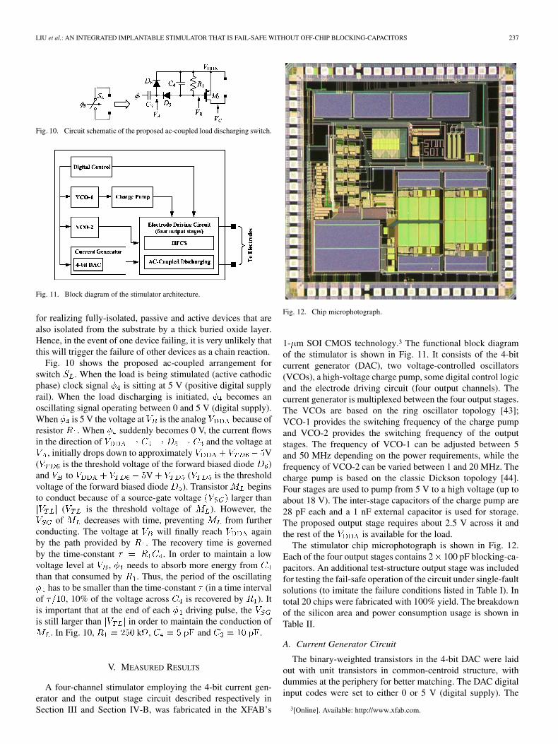
1- m SOI CMOS technology.3 The functional block diagramof the stimulator is shown in Fig. 11. It consists of the 4-bitcurrent generator (DAC), two voltage-controlled oscillators(VCOs), a high-voltage charge pump, some digital control logicand the electrode driving circuit (four output channels). Thecurrent generator is multiplexed between the four output stages.The VCOs are based on the ring oscillator topology [43];VCO-1 provides the switching frequency of the charge pumpand VCO-2 provides the switching frequency of the outputstages. The frequency of VCO-1 can be adjusted between 5and 50 MHz depending on the power requirements, while thefrequency of VCO-2 can be varied between 1 and 20 MHz. Thecharge pump is based on the classic Dickson topology [44].Four stages are used to pump from 5 V to a high voltage (up toabout 18 V). The inter-stage capacitors of the charge pump are28 pF each and a 1 nF external capacitor is used for storage.The proposed output stage requires about 2.5 V across it andthe rest of the is available for the load.
The stimulator chip microphotograph is shown in Fig. 12.Each of the four output stages contains 2 100 pF blocking-ca-pacitors. An additional test-structure output stage was includedfor testing the fail-safe operation of the circuit under single-faultsolutions (to imitate the failure conditions listed in Table I). Intotal 20 chips were fabricated with 100% yield. The breakdownof the silicon area and power consumption usage is shown inTable II.
A. Current Generator Circuit
The binary-weighted transistors in the 4-bit DAC were laidout with unit transistors in common-centroid structure, withdummies at the periphery for better matching. The DAC digitalinput codes were set to either 0 or 5 V (digital supply). The
3[Online]. Available: http://www.xfab.com.
238 IEEE TRANSACTIONS ON BIOMEDICAL CIRCUITS AND SYSTEMS, VOL. 2, NO. 3, SEPTEMBER 2008
TABLE IIBREAKDOWN OF AREA AND POWER USAGE
Fig. 13. Measured output current versus DAC digital input code for three �settings.
amplifier in Fig. 7 was a pMOS-input folded cascode amplifier[39] with a dc gain of 72 dB, a unity gain bandwidth of 9 MHzand a slew-rate of 8.33 V s. The amplifier was compensatedby a 4 pF capacitor at its output node and was stable for allvalues of the stimulating current. The area of the 4-bit DAC asnoted in Table II is 0.09 mm , 83% of which is occupied by theamplifier.
The bias voltage was not included in the prototype chipand was provided externally. However, a supply-independentand temperature-independent bias circuit can be easily designed[39]. With a of 176 mV at the noninverting input of theamplifier, the measured drain-source resistance of theunity transistors is in the range of 2.59-2.71 k across all chips.Fig. 13 shows the 4-bit current generator output current versusDAC digital input for three settings. The integral nonlin-earity (INL) and differential nonlinearity (DNL) of the DACfor the case of 1 mA full-scale current, is shown in Fig. 14.The maximum INL error is only 0.065 LSB while the max-imum DNL error is only 0.032 LSB. It is also possible to changethe output current by keeping the digital input constant andchanging . Fig. 15 shows the output current versus forthe digital input code 1111. The nonlinearity, calculated by themethod described in [45], is only 1.25% over the entire range.
The output characteristic of the current generator is shown inFig. 16 for the DAC input codes 0011, 0111 and 1111 (all for
mV). The curves show that the circuit requires only
Fig. 14. Measured DNL and INL for 1 mA full-scale current.
Fig. 15. Measured output current versus bias voltage � . The digital inputcode is set to 1111.
0.22 V, 0.28 V and 0.41 V across its output to respectively main-tain constant currents of 200 A, 466.7 A and 1 mA. The cir-cuit in [26] requires about 0.7 V to maintain a constant currentof 200 A. This demonstrates that the proposed current gener-ator circuit has indeed very small voltage compliance even forcurrents in the milliampere range. The output impedance of thecircuit is above the accuracy of the measurement equipment. Ca-dence Spectre simulations indicate that the output impedance isapproximately 100 M at 1 mA and remains greater than 40M for an output voltage as low as 0.6 V.
The temperature coefficient of the output current (for 1 mAfull-scale current) in simulation is 4.4 A C. However, tem-perature effects are less important for an implanted device dueto the stable temperature conditions in the body [21]. The pro-posed current generator circuit requires a well regulated digitalsupply voltage for driving the gates of the DAC transis-tors. The sensitivity of the output current to variation (for1 mA full-scale current) in simulation is about 150 nA/mV. For
, all fabricated samples showed no more than 1%
LIU et al.: AN INTEGRATED IMPLANTABLE STIMULATOR THAT IS FAIL-SAFE WITHOUT OFF-CHIP BLOCKING-CAPACITORS 239
TABLE IIICOMPARISON OF VARIOUS CURRENT GENERATOR CIRCUITS FOR IMPLANTABLE NEURAL STIMULATORS
Fig. 16. Measured output characteristic curves showing the large outputvoltage compliance of the current generator circuit.
deviation from the nominal 1 mA full-scale output current. Al-though analog mismatch, temperature and digital supply varia-tions cause some deviation of the output current from its nom-inal value, this is not important because in our application (stim-ulation of the lumbo-sacral nerve roots which can be used torestore lower-body function to paraplegics after spinal cord in-jury) we can compensate for it by fine control of the pulsewidth(in 10 s steps) of the active cathodic current.
Since the proposed current generator circuit achieves high lin-earity without any biasing or compensation circuits, it is veryarea-efficient. Table III compares the performance of variousneural stimulator current generator circuits (assuming 4-bit im-plementation) in terms of linearity, voltage compliance, outputimpedance and silicon area. The proposed circuit is the best op-tion where high linearity, small voltage compliance and smallsilicon area are of prime importance.
B. Output Stage With HFCS
The output stage was first tested with various RC load com-binations with impedances between 1 and 10 k . For the largerloads, the internal charge pump was used to provide the analogpower supply . Fig. 17 shows the measured current andvoltage waveforms for a series RC load (8 k ) for twocomplete stimulation cycles. The repetition rate was 25 Hz with1 ms active cathodic phase, 1 ms inter-phase delay (between thecathodic phase and the anodic phase) and 37 ms passive anodicphase. The current from the current generator was set to 1 mA.For this measurement the output of the charge pump was about15 V.
Fig. 17. Measured current and voltage waveforms. (a). Stimulus currentthrough the RC load; (b) Voltage across the RC load.
Fig. 18. Measured voltage for 100%, 40%, and 20% discharging current.
As another illustration, Fig. 18 shows the measured voltageacross a series 500 load (the impedance of this combi-nation is similar to that of a book electrode [46]). An external 6V power supply (i.e., V) was used for this measure-ment since using the internal 4-stage charge pump for smallerthan 10 V was not efficient. The timing profile was kept thesame as that in Fig. 17. The amplitude of the active cathodiccurrent was kept at 1 mA while the amplitude of the initial pas-sive anodic current was limited to 100%, 40%, and 20% of the

240 IEEE TRANSACTIONS ON BIOMEDICAL CIRCUITS AND SYSTEMS, VOL. 2, NO. 3, SEPTEMBER 2008
Fig. 19. Measured voltages of � and � for Fig. 10.
amplitude of the cathodic current, respectively, by appropriatedimensioning of the discharging transistor or by an ex-ternal resistor (of an appropriate value) in series with the dis-charging transistor. A small discharging current would be thecase in practice to ensure that stimulation does not occur inthe second phase. As shown in the figure, the smaller the dis-charging current, the longer it takes to discharge.
Fig. 19 shows the operation of the proposed ac-coupled tech-nique for the load discharging switch. For testing, a 10 k re-sistor was connected at node in Fig. 10. The other end of theresistor was connected to the negative supply (0 V). The voltagewaveforms and are shown, respectively, in Fig. 18 (for
). When the 1 MHz oscillating signal is applied at, transistor conducts. Thus, the ON level of is close
to [see Fig. 18(b)]. The slight difference is caused by thedrain-source voltage drop of . Each output stage circuit (con-sists of HFCS stage and ac-coupled discharging circuit) occu-pies an area of 0.38 mm .
Fig. 20 shows the measured voltage waveforms across theblocking-capacitor ( or in Fig. 9) for different switchingfrequencies at 0.5 mA stimulation. These waveforms wereobtained using on-chip buffers. The voltage drop across eachblocking-capacitor is proportional to the period of the high-fre-quency signal and is independent of the duration of the completeactive cathodic phase. As seen in the figure, 20 MHz results inapproximately 3 times less voltage drop across the blocking-ca-pacitor than 7 MHz. However, it can be shown that there is anoptimized switching frequency for minimal power consumptiondue to the energy used to charge and discharge the two smallblocking-capacitors and the dynamic power of the switching ac-tion of the four switches ( in Fig. 9). The optimizedfrequency to achieve minimum power consumption in the stim-ulation phase (assuming ideal diodes with no stray capacitance)is given by
(9)
Fig. 20. Showing measured voltage waveform across the blocking-capacitorfor different switching frequencies.
where is the small blocking-capacitor ( or ) and andare respectively the total capacitance and the voltage pulse
amplitute at the gates of the four switches in Fig. 9. Inthe fabricated stimulator, , (480 fFper switch) and and so for mA, theusing (9) is 10.2 MHz.
C. Testing of Single-Fault Failures
The fail-safe operation of the stimulator output stage undersingle-fault conditions has been both simulated and measuredwith an on-chip test structure in which extra switches have beenadded in series and in parallel with the components listed inTable IV. Because of the symmetrical structure of the proposedoutput stage circuit, only failures in the left branch are pre-sented. As shown in Table IV, for all failures the output currentis never more than the current in normal operation. The mea-sured current is higher than the estimation when it is expectedto be 50% due to the limited slew-rate of the current generatoramplifier which is not able to fully switch on and off at thisspeed. As a result, the current generator pushes more than halfthe proper current into the load when only one half of the circuitis functional.
D. Measurement of Direct Current in Vitro
Fig. 21 shows the setup used to measure the direct currentflowing from the stimulator through a dipole book electrode ina saline bath (0.9% saline). The method was adopted from [11].In the figure, , , and are off-chip compo-nents added for the test. is an external resistance box usedto adjust the amplitude of the initial current in the passive dis-charging phase to some ratio of the amplitude of the current inthe active cathodic phase. The voltage across (100 ) is usedto monitor the biphasic current through the electrodes. is a70 low-leakage polyester capacitor, is a high-precision

LIU et al.: AN INTEGRATED IMPLANTABLE STIMULATOR THAT IS FAIL-SAFE WITHOUT OFF-CHIP BLOCKING-CAPACITORS 241
TABLE IVSIMULATED AND MEASURED OUTPUT CURRENT FOR DIFFERENT FAILURE
CONDITIONS
Fig. 21. Direct current measurement setup.
107 k resistor and the voltmeter is an HP 34401A 6-digit mul-timeter which has 10 M input resistance. The current wave-form is low-pass filtered by the combined resistance and capac-itance (time constant 7.4 s) and the direct current is the measuredvoltage divided by 105.9 k . Each of the two U-shaped Pt elec-trodes in the book had an area of about 7 mm . A Pt electrodehas a maximum charge density of 0.15 mC/cm [47]. The chargedensity in the experiment was only about 10% of the maximumvalue.
To be consistent with the previous specification, the leadingcathodic current pulse was always 1 mA and 1 ms while theinter-phase delay and the inter-cycle delay (between anodicphase and next cycle’s cathodic phase) were always kept at 1ms. Table V shows the measured direct current for differentstimulation rates and amplitudes of the initial current in thepassive anodic phase. As shown, the direct current increaseswith increasing stimulation rate and decreasing amplitudeof the initial current in the passive cathodic phase, but arenever higher than 12.2 nA. To our knowledge, FES never usesfrequencies higher than 50 Hz [48] so this is a worst-case condi-tion and corresponds to leakage of 0.024% of the charge in the
TABLE VMEASURED DIRECT CURRENT FOR DIFFERENT STIMULATION RATES AND
DISCHARGING CURRENTS
Fig. 22. Tank experimental setup.
stimulation pulse. This result shows that passive dischargingwithout any large blocking-capacitors but relying only on thecapacitance of the Pt electrodes can give satisfactory results.With a 30 polyester blocking-capacitor added in the testcircuit, the measured direct current was reduced to about 2 nA.
E. Stimulation of Frog Nerve in Vitro
Finally, to verify the practical working of our HFCS stim-ulator chip, we performed an in vitro experiment on the sci-atic nerve of a frog in Ringer’s solution. The stimulating elec-trode used was a tripolar book electrode,4 configured as a dipole,while the recording electrode was a dipole hook electrode (in-house made). The recording amplifier was an ISO-DAM8A byWorld Precision Instruments. For these experiments the stimu-lator analog power supply was set to 6 V. The tank setup for thisexperiment is shown in Fig. 22 where we can see the frog nervein the middle, the book electrode on the left and the recordinghook electrode on the right.
Fig. 23 shows an example of the action potential recorded atthe output of the recording amplifier (amplifier gain of 10). Forthis recording, the stimulus pulse generated by our stimulatorchip was a 1 ms, 1 mA stimulation phase and 10 ms recuperationphase, separated by 1 ms inter-phase delay. The stimulation ranat 20 Hz. The HFCS switching signal and the ac-coupled oscil-lating discharging signal were 10 and 1 MHz, respectively. Themeasured average power consumption of the stimulator outputstage was 200 W (using an external power supply), a fifth ofwhich was due to the HFCS switching and ac-coupled oscilla-tion. The average power at the stimulation load was measuredto be 72 W. Hence, for this stimulation the power efficiency
4Made by Finetech Medical Ltd, Welwyn Garden City, Herts, UK.

242 IEEE TRANSACTIONS ON BIOMEDICAL CIRCUITS AND SYSTEMS, VOL. 2, NO. 3, SEPTEMBER 2008
Fig. 23. Recorded action potential from the frog nerve initiated by the stimu-lator chip.
Fig. 24. Strength-duration curve obtained from the in vitro experiment.
was 36%. Fig. 24 shows the strength-duration5 curve obtainedusing our stimulator chip. We noted no appreciable differencebetween the nerve stimulation thresholds obtained using ourHFCS stimulator chip and using a conventional stimulator witha large off-chip blocking-capacitor.
VI. CONCLUSION
We have introduced two circuit techniques to miniaturize theoutput stage of implantable neural stimulators. The first tech-nique is a new current generator circuit with major advantagesover previous works. The circuit utilizes MOS transistors inthe deep triode region as linearized voltage-controlled resistorsand features high linearity, small voltage compliance, highoutput impedance and small implementation area. The secondtechnique is a new stimulator output stage circuit with on-chipblocking-capacitor protection. The circuit utilizes the HFCStechnique which allows the physical size of the stimulator im-plant to be dramatically reduced and still be fail-safe. To verify
5A graph relating the intensity of an electrical stimulus to the length of timeit must flow to be effective.
the circuit ideas we have implemented a four-channel stimulatorchip in XFAB’s 1- m SOI CMOS technology and tested it invitro. The benefits of miniaturization offered by the proposedtechniques are a major step towards developing a high-densityneural stimulation interface for the lumbro-sacral spinal roots.It is hoped that this will restore many more functions to peoplewith spinal cord injury than is currently possible.
ACKNOWLEDGMENT
The authors would like to thank Dr. A. Vanhoest for helpingwith the in vitro experiment and P. Langlois for helpful discus-sions regarding the circuit design. They also wish to acknowl-edge the anonymous reviewers as their detailed and thoroughreview helped to significantly improve the content and qualityof the manuscript.
REFERENCES
[1] P. P. H. Peckham and J. S. Knutson, “Functional electrical stimulationfor neuromuscular applications,” Annu. Rev. Biomed. Eng., vol. 7, pp.327–360, Aug. 2005.
[2] N. Donaldson, D. Rushton, and T. Tromans, “Neuroprostheses forleg function after spinal-cord injury,” Lancet, vol. 350, no. 9079, pp.711–712, Sep. 1997.
[3] T. A. Perkins, N. Donaldson, N. A. C. Hatcher, I. D. Swain, and D. E.Wood, “Control of leg-powered paraplegic cycling using stimulation ofthe lumbo-sacral anterior spinal nerve roots,” IEEE Trans. Neural Syst.Rehabil. Eng., vol. 10, no. 3, pp. 158–164, Sep. 2002.
[4] N. J. M. Rijkhoff, J. Holsheimer, E. L. Koldewijn, J. J. Struijk, P. E. V.v. Kerrebroeck, F. M. J. Debruyne, and H. Wijkstra, “Selective stim-ulation of sacral nerve roots for bladder control: A study by computermodeling,” IEEE Trans. Biomed. Eng., vol. 41, no. 5, pp. 413–424, May1994.
[5] N. de N.Donaldson and P. E. K. Donaldson, “When are actively bal-anced biphasic (‘Lilly’) stimulating pulses necessary in a neurologicalprosthesis? II. pH changes; noxious products; electrode corrosion; dis-cussion,” Med. Biol. Eng. Comput., vol. 24, no. 1, pp. 50–56, Jan. 1986.
[6] C. Huang, P. Carter, and R. Shepherd, “Stimulus induced pH changesin cochlear implants: An in vitro and in vivo study,” Annals Biomed.Eng., vol. 29, no. 9, pp. 791–802, Sep. 2001.
[7] C. M. Zierhofer, I. J. H.-Desoyer, and E. S. Hochmair, “Electronic de-sign of a cochlear implant for multichannel high-rate pulsatile stimu-lation strategies,” IEEE Trans. Neural Syst. Rehabil. Eng, vol. 3, no. 1,pp. 112–116, Mar. 1995.
[8] M. Bugbee, N. de N.Donalsdon, A. Lickel, N. J. Rijkhoff, and J. Taylor,“An implant for chronic selective stimulation of nerves,” Med. Eng.Phys., vol. 23, no. 1, pp. 29–36, Jan. 2001.
[9] J. D. Techer, S. Bernard, Y. Bertrand, G. Cathebras, and D. Guiraud,“New implantable stimulator for the FES of paralyzed muscles,” inProc. 30th Eur. Solid-State Circuits Conf. (ESSCIRC’04), Leuven, Bel-gium, 2004, pp. 455–458.
[10] P. R. Troyk and N. de N.Donaldson, “Implantable FES systems: Whatis needed?,” Neuromodulation, vol. 4, no. 4, pp. 196–204, Oct. 2001.
[11] C. Q. Huang, R. K. Shepherd, P. M. Center, P. M. Seligman, and B.Tabor, “Electrical stimulation of the auditory nerve: Direct currentmeasurement in vivo,” IEEE Trans. Biomed. Eng., vol. 46, no. 4, pp.461–469, Apr. 1999.
[12] G. J. Suaning and N. H. Lovell, “CMOS neurostimulation ASIC with100 channels, scaleable output, and bidirectional radio-frequencytelemetry,” IEEE Trans. Biomed. Eng., vol. 48, no. 2, pp. 248–260,Feb. 2001.
[13] N. Donaldson and P. Donaldson, “When are actively balanced biphasic(‘Lilly’) stimulation pulses necessary in a neurological prosthesis? Ihistorical background; Pt resting potential; Q studies,” Med. Biol. Eng.Comput., vol. 24, pp. 41–49, Jan. 1986.
[14] S. B. Brummer and M. J. Turner, “Electrochemical considerations forsafe electrical stimulation of the nervous system with platinum elec-trodes,” IEEE Trans. Biomed. Eng., vol. BME-24, no. 1, pp. 59–63,Jan. 1977.
[15] L. S. Robblee, J. L. Lefko, and S. B. Brummer, “Activated Ir: An elec-trode suitable for reversible charge injection in saline solution,” J. Elec-trochem. Soc., vol. 130, no. 3, pp. 731–733, Mar. 1983.

LIU et al.: AN INTEGRATED IMPLANTABLE STIMULATOR THAT IS FAIL-SAFE WITHOUT OFF-CHIP BLOCKING-CAPACITORS 243
[16] J.-J. Sit and R. Sarpeshkar, “A low-power blocking-capacitor-freecharge-balanced electrode-stimulator chip with less than 6 nA DCerror for 1-mA full-scale stimulation,” IEEE Trans. Biomed. CircuitsSyst., vol. 1, no. 3, pp. 172–183, Sep. 2007.
[17] M. Ghovanloo and K. Najafi, “A wireless implantable multichannelmicrostimulating system-on-a-chip with modular architecture,” IEEETrans. Neural Syst. Rehab. Eng., vol. 15, no. 3, pp. 449–457, Sep. 2007.
[18] C. Donfack, M. Sawan, and Y. Savaria, “Implantable measurementtechnique dedicated to the monitoring of electrode-nerve contact inbladder stimulators,” Med. Biol. Eng. Comput., vol. 38, no. 4, pp.465–468, Jul. 2000.
[19] D. Hou, A. Asres, Z. Zhou, and Z. Zhu, “Stimulator for real time con-trol of paralyzed muscles during functional electrical stimulation,” inProc. 3rd IEEE Int. Conf. Electron. Circuits Syst. (ICECS ’96), Rodos,Greece, 1996, vol. 2, pp. 1096–1099.
[20] H. McDermott, “An advanced multiple channel cochlear implant,”IEEE Trans. Biomed. Eng., vol. 36, pp. 789–797, Jul. 1989.
[21] M. Ortmanns, A. Rocke, M. Gehrke, and H. Tiedtke, “A 232-channelepiretinal stimulator ASIC,” IEEE J. Solid-State Circuits, vol. 42, no.12, pp. 2946–2959, Dec. 2007.
[22] K. R. Laker and W. M. C. Sansen, Design of Analog Integrated Circuitsand Systems. New York: McGraw-Hill, 1994, pp. 380–380.
[23] X. Liu, A. Demosthenous, and N. Donaldson, “A stimulator outputstage with capacitor reduction and failure-checking techniques,” inProc. 2006 IEEE Int. Symp. Circuits Syst. (ISCAS’06), Kos Island,Greece, May 2006, pp. 641–644.
[24] X. Liu, A. Demosthenous, and N. Donaldson, “A fully integrated fail-safe stimulator output stage dedicated to FES stimulation,” in Proc.2007 IEEE Int. Symp. Circuits Syst. (ISCAS’07), New Orleans, LA,May 2007, pp. 2076–2079.
[25] M. Sivaprakasam, L. Wentai, M. S. Humayun, and J. D. Weiland, “Avariable range bi-phasic current stimulus driver circuitry for an im-plantable retinal prosthetic device,” IEEE J. Solid-State Circuits, vol.40, no. 3, pp. 763–771, Mar. 2005.
[26] M. Ghovanloo and K. Najafi, “A compact large voltage-compliancehigh output-impedance programmable current source for implantablemicrostimulators,” IEEE Trans. Biomed. Eng., vol. 52, no. 1, pp.97–105, Jan. 2005.
[27] M. B. Bugbee, “An Implantable Stimulator for Selective Stimulation ofNerves,” Ph.D. dissertation, University College London, London, UK,2001.
[28] T. Cameron, T. L. Liinamaa, G. E. Loeb, and F. J. R. Richmond, “Long-term biocompatibility of a miniature stimulator implanted in felinehind limb muscles,” IEEE Trans. Biomed. Eng., vol. 45, no. 8, pp.1024–1035, Aug. 1998.
[29] G. E. Loeb and F. J. R. Richmond, BION Implants for Therapeutic andFunctional Electrical Stimulation, J. K. Chapin, K. A. Moxon, and G.Gaal, Eds. Boca Raton, FL: CRC Press, 2000, ch. Neural Prosthesesfor Restoration of Sensor and Motor Function, pp. 75–99.
[30] P. R. Singh, “Micro-Stimulator Design for Retinal Prostheses,” M.Sc.thesis, North Carolina State Univ., Raleigh, 2002.
[31] T. Klenzner, F. Knapp, F. Rohner, E. von Wallenberg, H. Mauch, P.Pedersen, A. Aschendorff, R. Laszig, and J. Lutterbach, “Influence ofionizing radiation on nucleus 24 cochlear implants,” Otol. Neurotol.,vol. 26, no. 4, pp. 661–667, Jul. 2005.
[32] B. Ziaie, M. D. Nardin, A. R. Coghlan, and K. Najafi, “A single-channelimplantable microstimulator for functional neuromuscular stimula-tion,” IEEE Trans. Biomed. Eng., vol. 44, no. 10, pp. 909–920, Oct.1997.
[33] M. Sivaprakasam, L. Wentai, W. Guoxing, J. D. Weiland, and M. S.Humayun, “Architecture tradeoffs in high-density microstimulators forretinal prosthesis,” IEEE Trans. Circuits Syst. I: Reg. Papers, vol. 52,no. 12, pp. 2629–2641, Dec. 2005.
[34] W. Liu, K. Vichienchom, M. Clements, S. C. DeMarco, C. Hughes, E.McGucken, M. S. Humayun, E. D. Juan, J. D. Weiland, and R. Green-berg, “A neuro-stimulus chip with telemetry unit for retinal prostheticdevice,” IEEE J. Solid-State Circuits, vol. 35, no. 10, pp. 1487–1497,Oct. 2000.
[35] K. Arabi and M. A. Sawan, “Electronic design of a multichannel pro-grammable implant for neuromuscular electrical stimulation,” IEEETrans. Neural Syst. Rehab. Eng., vol. 7, no. 2, pp. 204–214, Jun. 1999.
[36] S. C. DeMarco, L. Wentai, P. R. Singh, G. Lazzi, M. S. Humayun, andJ. D. Weiland, “An arbitrary waveform stimulus circuit for visual pros-theses using a low-area multibias DAC,” IEEE J. Solid-State Circuits,vol. 38, no. 10, pp. 1679–1690, Oct. 2003.
[37] K. E. Jones and R. A. Normann, “An advanced demultiplexing systemfor physiological stimulation,” IEEE Trans. Biomed. Eng., vol. 44, no.12, pp. 1210–1220, Dec. 1997.
[38] S. Boyer, M. Sawan, M. Abdel-Gawad, S. Robin, and M. M. Elhilali,“Implantable selective stimulator to improve bladder voiding: Designand chronic experiments in dogs,” IEEE Trans. Neural Syst. Rehab.Eng., vol. 8, no. 4, pp. 464–470, Dec. 2000.
[39] B. Razavi, Design of Analog CMOS Integrated Circuits. New York:McGraw-Hill, 2000.
[40] M. Schaldach, “Present state and future trends in electrical heart stim-ulation,” Med. Progr. Technol., vol. 13, no. 2, pp. 85–1002, 1987.
[41] Private Communication With X-FAB Semiconductor Foundries AG,Germany, 2006.
[42] Integrated Passive Component Technology, R. K. Ulrich and L. W.Schaper, Eds. Hoboken, NJ: Wiley-IEEE Press, 2003.
[43] R. J. Baker, CMOS: Circuit Design, Layout, and Simulation, 2nd ed.Hoboken, NJ: Wiley-Interscience, 2005.
[44] J. F. Dickson, “On-chip high-voltage generation in nMOS integratedcircuits using an improved voltage multiplier technique,” IEEE J. Solid-State Circuits, vol. SC-11, no. 3, pp. 374–378, Jun. 1976.
[45] S. L. Garverick and C. G. Sodini, “Large-signal linearity of scaledMOS transistors,” IEEE J. Solid-State Circuits, vol. SC-22, no. 4, pp.282–286, Apr. 1987.
[46] I. Pachnis, A. Demosthenous, and N. Donaldson, “Passive neutraliza-tion of myoelectric interference from neural recording tripoles,” IEEETrans. Biomed. Eng., vol. 54, no. 6, pp. 1067–1074, Jun. 2007.
[47] , B. He, Ed., Neural Engineering. Norwell, MA: Kluwer, 2005, pp.8–8.
[48] A. Kralj and T. Bajd, Functional Electrical Stimulation: Standing andWalking After Spinal Cord Injury. Boca Raton, FL: CRC Press, 1989.
Xiao Liu (S’05) was born in Chengdu, China, in1981. He received the B.Eng. degree in informa-tion engineering from Xi’an Jiaotong University(XJTU), Xi’an, China, in 2003, the M.Sc. degreein microelectronics systems design from Universityof Southampton, Southampton, U.K., in 2004, andis currently working towards the Ph.D. degree atUniversity College London (UCL), London, U.K.
Since 2006, he has been a Research Assistant in theDepartment of Electronic and Electrical Engineering,UCL. His main research interests include analog in-
tegrated circuit design and biomedical electronics for implanted devices, espe-cially for functional electrical stimulation applications.
Andreas Demosthenous (S’94–M’99–SM’05) wasborn in Nicosia, Cyprus, in 1969. He received theB.Eng. degree in electrical and electronic engineeringfrom the University of Leicester, Leicester, U.K., in1992, the M.Sc. degree in telecommunications tech-nology from Aston University, Birmingham, U.K., in1994, and the Ph.D. degree in electronic and elec-trical engineering from University College London(UCL), London, U.K., in 1998.
From 1998 to 2000, he held a Postdoctoral Re-search Fellow position with the Department of Elec-
tronic and Electrical Engineering, UCL. In 2000, he was appointed to the aca-demic faculty of the same department, where he is currently a Reader and headsthe Analog and Biomedical Electronics Research Group. His main area of re-search is analog and mixed-signal integrated circuits for biomedical, commu-nication, sensor and signal processing applications. He has published over 90articles in journals and international conference proceedings.
Dr. Demosthenous is a member of the Analog Signal Processing TechnicalCommittee (ASPTC) and the Biomedical Circuits and Systems (BioCAS)Technical Committee of the IEEE Circuits and Systems (CAS) Society. Heis also a member of the U.K. Engineering and Physical Sciences ResearchCouncil (EPSRC) Peer Review College. He is an Associate Editor for the IEEETRANSACTIONS ON CIRCUITS AND SYSTEMS I: REGULAR PAPERS and an Asso-ciate Editor for the IEEE CAS Society Newsletter. He is on the InternationalAdvisory Board for Physiological Measurement. In 2006 and 2007, he was anAssociate Editor for the IEEE TRANSACTIONS ON CIRCUITS AND SYSTEMS II:EXPRESS BRIEFS.

244 IEEE TRANSACTIONS ON BIOMEDICAL CIRCUITS AND SYSTEMS, VOL. 2, NO. 3, SEPTEMBER 2008
Nick Donaldson received the M.A. degree in engi-neering and electrical sciences at Cambridge Univer-sity, Cambridge, U.K.
From 1977 to 1992, he worked for the MedicalResearch Council, Neurological Prostheses Unit,London, U.K., under the direction of Prof. G. bS.Brindley. In that period, his main field of researchwas the technology and use of implanted device forthe restoration of useful leg function to paraplegics.Since 1992, he has been Head of the Implanted De-vices Group at University College London, London,
U.K. He has been Principal Investigator for many projects related to implanteddevices and functional electrical stimulation. He is also a Professor in theUniversity. His research interests now includes the development of implanteddevices that use natural nerve signals as inputs, especially for preventingincontinence; stimulators of nerve roots; the use of electrical stimulation forrecreational exercise of paralyzed legs; and methods to encourage functionalneurological recovery after injury.