ieee journal of solid-state circuits, vol. 45, no. 4
TRANSCRIPT

IEEE JOURNAL OF SOLID-STATE CIRCUITS, VOL. 45, NO. 4, APRIL 2010 899
A 0.6 mW/Gb/s, 6.4–7.2 Gb/s Serial Link ReceiverUsing Local Injection-Locked Ring Oscillators
in 90 nm CMOSKangmin Hu, Student Member, IEEE, Tao Jiang, Student Member, IEEE, Jingguang Wang,
Frank O’Mahony, Member, IEEE, and Patrick Yin Chiang, Member, IEEE
Abstract—This paper describes a quad-lane, 6.4–7.2 Gb/s seriallink receiver prototype using a forwarded clock architecture. Anovel phase deskew scheme using injection-locked ring oscillators(ILRO) is proposed that achieves greater than one UI of phase shiftfor multiple clock phases, eliminating phase rotation and interpo-lation required in conventional architectures. Each receiver, opti-mized for power efficiency, consists of a low-power linear equalizer,four offset-cancelled quantizers for 1:4 demultiplexing, and an in-jection-locked ring oscillator coupled to a low-voltage swing, globalclock distribution. Measurement results show a 6.4–7.2 Gb/s datarate with BER 10 �� across 14 cm of PCB, and also an 8.0 Gb/sdata rate through 4 cm of PCB. Designed in a 1.2 V, 90 nm CMOSprocess, the ILRO achieves a wide tuning range from 1.6–2.6 GHz.The total area of each receiver is 0.0174 mm�, resulting in a mea-sured power efficiency of 0.6 mW/Gb/s.
Index Terms—Injection-locked oscillator, receiver, serial link.
I. INTRODUCTION
T HE demand for massively parallel, high speed serial linkshas recently intensified due to the large amount of off-chip
bandwidth required for future multi-core processing and net-working applications [1]–[3]. For example, microprocessor in-dustry standards such as Hyper Transport [4] and Quick Path[5] require tens of high-speed serial links with a combined band-width greater than 200 Gb/s. In addition, recent chipsets for net-working switches require off-chip I/O bandwidths of 2.4 Tb/s[3]. Due to the continual scaling of transistors in future CMOSprocesses, today’s state-of-the art serial links can achieve tensof Gb/s per pin [6]–[8]. While such bandwidth/pin is an impor-tant consideration for these next generation applications, energyefficiency per link is the critical metric as there may exist tensto hundreds of these links on a single chip [1], [10].
In contrast to legacy backplane applications that exhibitchannel losses greater than 20 dB at Nyquist frequencies [11],
Manuscript received August 27, 2009; revised November 19, 2009. Currentversion published March 24, 2010. This paper was approved by Guest EditorMasayuki Mizuno. This work was supported by Intel Corporation.
K. Hu, T. Jiang, and P. Y. Chiang are with the School of Electrical Engi-neering and Computer Science, Oregon State University, Corvallis, OR 97331USA (e-mail: [email protected]; [email protected]).
J. Wang was with the School of Electrical Engineering and Computer Science,Oregon State University. He is now with Broadcom Corporation, Irvine, CA92618 USA.
F. O’Mahony is with Intel Corporation, Hillsboro, OR 97124 USA.Color versions of one or more of the figures in this paper are available online
at http://ieeexplore.ieee.org.Digital Object Identifier 10.1109/JSSC.2010.2040116
these future applications may optimize transmission line char-acteristics for better signal integrity (i.e. better connectors andshorter distances), such that channel losses are moderate andtherefore do not require complex equalization [9]. Therefore,the goal for these short-haul, highly parallelized, chip-to-chipsignaling is to achieve high power efficiency (mW/Gb/s) whilerequiring only minimal equalization power.
Recent serial link receivers have shown significant improve-ments in power efficiency by focusing on reducing dynamicclock power using resonantly-tuned LC oscillators, both inglobal clock distribution [9], [12] and local clock demulti-plexing [8], [13]. In this paper, we present a multi-channelserial link receiver architecture that exhibits further improve-ments in dynamic clock power consumption by implementinga low-voltage swing, global clock distribution to multiple linklocations, where locally-tapped, injection-locked ring oscilla-tors (ILRO) are used to generate tunable quadrature samplingclocks for receiver demultiplexing [14].
The overview of this paper is as follows. Section II describesthe architectural considerations for receiver clocking and datarecovery (CDR). Next, in Section III, while most previousanalyses of injection-locked oscillator are only applicable toLC oscillators [15]–[18], we propose new analytical equationsthat enable the understanding of injection-locked, nonharmonicring oscillators, including the locking range, phase deskewability, and jitter performance. Details of the receiver circuitimplementation are described in Section IV. Section V pro-vides the measurement results of the test chip, ending with theconclusion in Section VI.
II. RECEIVER ARCHITECTURE OVERVIEW
Embedded clock and forwarded clock architectures are thetwo major CDR architectures for multi-Gb/s transceivers. In em-bedded clock architecture, the clock is directly recovered fromthe incoming data such that no extra clocking channel is re-quired. Therefore, the jitter of the recovered clock will track thatof the data within the CDR loop bandwidth. If there are multipleembedded clock serial links, each can work independently fromseparate frequency references. However, recovering clock fromthe data typically requires 2 oversampling, resulting in con-siderable overhead in power consumption [19].
Compared with the embedded clock architecture, forwardedclock architectures [20] reduce the power of clock recovery atthe expense of an additional forwarded link to deliver the trans-mitted mesochronous clock. However, if the chip I/O interface
0018-9200/$26.00 © 2010 IEEE
Authorized licensed use limited to: Texas A M University. Downloaded on April 02,2010 at 08:57:04 EDT from IEEE Xplore. Restrictions apply.

900 IEEE JOURNAL OF SOLID-STATE CIRCUITS, VOL. 45, NO. 4, APRIL 2010
Fig. 1. (a) Conventional forwarded clock receiver architecture and (b) proposedarchitecture using ILRO for multiple serial links.
requires many parallel serial lanes, the power and pin overheadof the additional forwarded clock can be amortized among allthe data links.
A conventional, forwarded clock receiver architecture [21] isshown in Fig. 1(a), which consists of the global clock distribu-tion, as well as the local delay/phase locked loop (DLL/PLL)to generate multiple time-interleaved phases. The proceedingphase rotator use these phases to interpolate the appropriatephase position for the receiver to sample the incoming data.In this architecture, significant power is spent in the receiverclocking and phase generation as each link needs a local, phaserotator-based PLL to deskew the clock phase for recovery of thedata [22]. For example, phase rotation alone occupies almosthalf the total receiver power in [9].
As an alternative to the phase rotator, injection-locked LC os-cillators (IL-LCO) can enable clock deskew ability with lesspower and a lower voltage swing for the global clock. Hence,injection-locking has recently been proposed for both clock dis-tribution [12], [23] and serial link receivers [8], [24]. As shownfrom the phase vector diagram in Fig. 2(a), when the frequencyof the injection signal is different from the free-runningfrequency of the signal in the LC tank, e(x), a phase deskew
will be generated between the resulting outputs and. The value depends on the frequency difference and
locking range, given by Alder’s equation [15]:
(1)
where is the phase difference between the resultant outputclock and the injection input clock, is the phase difference
Fig. 2. (a) Phase vector diagram (injection signal � ���, free-running tanksignal e(x) and resultant output � ���). (b) Deskew with different injectionstrength k, based on Adler’s equation.
between the free-running frequency and the resultant output,is the single-sided locking range, k is the injection strength
defined as the ratio of the injection current and the oscillator cur-rent, and is the frequency difference between and theinjection clock. Fig. 2(b) plots an example of the deskew phaseshift along the normalized frequency difference under three in-jection strength values.
Monolithic LC oscillators typically have better phase noiseand jitter performance than their ring oscillator counterpartsdue to the band-pass nature of LC tank resonators, rejectingout-of-band frequencies and filtering power supply inducednoise [25]. However, for highly-parallel serial link applications,per-channel, injection-locked LC oscillators are not desirable,as each receiver would require an individual on-chip inductor,resulting in significant area penalty. In addition, LC-basedoscillators exhibit very limited tuning range, may exhibitoscillator pulling due to magnetic coupling from adjacent LCoscillators [26], and do not scale well with continued tech-nology scaling.
Although the jitter performance of free-running ring oscil-lators is typically worse than LC oscillators, the large jittertransfer bandwidth of injection locking can suppress andhigh-pass filter a large amount of oscillator phase noise, as willbe described in Section III. Therefore, this work proposes a newforwarded clock receiver architecture using injection-lockedring oscillators (ILRO), as shown in Fig. 1(b), to deskew theclock used to sample the incoming data.
Compared with the conventional receiver architecture, theILRO can achieve large phase deskew ability without the poweroverhead required for the combined DLL, PLL and phase inter-polation. Second, it can lock to relatively small voltage swingsof the injected global clock, saving power in the clock distri-bution. Third, the ILRO can achieve faster phase locking than a
Authorized licensed use limited to: Texas A M University. Downloaded on April 02,2010 at 08:57:04 EDT from IEEE Xplore. Restrictions apply.

HU et al.: SERIAL LINK RECEIVER USING LOCAL INJECTION-LOCKED RING OSCILLATORS IN 90 nm CMOS 901
conventional PLL because while the loop bandwidth of a PLL islimited to approximately 1/10 of the reference clock [26], injec-tion-locking exhibits non-linear loop bandwidth characteristics.
Unfortunately, as shown in Fig. 2(b), nonlinearity can be ob-served in the deskew steps at the edge of locking range, when
reaches around . However, the linear deskew regioncan be increased as the injection strength k increases. To furtheravoid the use of the nonlinear deskew region, each receiver uses1:4 demultiplexing, implemented with four quantizers clockedby quadrature sampling. Therefore, only phase deskewrange of the ring oscillator is required to enable each quadraturephase to achieve full UI range, limiting the deskew to only thelinear region.
Compared with the IL-LCO, ILRO consumes less siliconarea, larger tuning range, inherent multi-phase generation,and scalability to future CMOS processes. However, becauseprevious analysis on the injection-locking phenomenon is ap-plicable only to tank-based oscillators, new analysis is neededto further understand the behavior of the proposed ILRO.
III. ANALYSIS ON INJECTION-LOCKING RING OSCILLATORS
A. Previous Approaches
Several methods have been proposed in previous worksto analyze injection locking in oscillators including: thephasor-based Adler’s equation, the perturbation-based projec-tion vector (PPV) method, and the waveform-based time-do-main derivation.
The classic Adler’s equation [15] expresses the oscillator be-havior under injection locking by using a phasor vector diagram,as shown in (1) and Fig. 2. Various time-domain solutions toAdler’s equation are discussed in [16]–[18]. However, two mainfactors prevent this approach from being applicable to ring os-cillators. First, the output waveform of ring oscillators usuallydoes not exhibit sine wave behavior; however, the adoption of avector-based analysis relies on the assumption that there existsonly a single dominant frequency component [28]. Second, it isrequired to know the quality factor Q in order to solve in(1), which is not well defined for nonharmonic ring oscillators.
The PPV [27] and the transient waveform-based methods [28]are capable of analyzing both LC and ring oscillators. How-ever, the PPV method requires a full circuit description at boththe transistor and numerical levels, and only the expression forlocking range is derived [27]. The analysis in [28] providesgood insight into analyzing injection locking in the time do-main. However, neither of these two methods gives an analyt-ical expression for evaluating the jitter performance of injec-tion-locked oscillators.
B. Proposed Approach for ILRO Analysis
Since Adler’s equation is still quite simple and is provenuseful for capturing the LC oscillator behavior in both the fre-quency and time domains, this work presents an expansion toAdler’s equation that overcomes the two limitations mentionedabove, making it suitable for injection-locked ring oscillators.
Fig. 3. Superposition of waveforms.
By revisiting the process of Adler’s derivation [15], it can beobserved:
(2)
Note that (2) is held for both LC and ring oscillators, as nei-ther the assumption of Q nor a vector diagram approach has beenapplied yet. Next, alternative methods for finding as wellas the relationship between and are presented.
First, can be solved directly from the small signalmodel of each delay cell. Assuming each delay cell contributesone dominant 3 dB pole, the loop transfer function H of anN-stage ring oscillator is
(3)
such that its phase and derivative are
(4)
(5)
Equation (5) is obtained by noting that each delay stage ex-hibits a phase shift equal to . Similaranalysis can lead to an equivalent definition of Q for ring oscil-lators as shown in [29].
Second, the phase relationship can be obtained by superposi-tion of waveforms in the time-domain rather than using a vectordiagram; this enables a general analysis for any arbitrary wave-form. As shown in Fig. 3, the proposed derivation assumes thatthe small-swing injection clock remains like a sine-wave,but the waveform shape of the free-running ring oscillator e(x)resembles a trapezoid. Hence, this trapezoidal model reflects theactual waveform of a nonharmonic ring oscillator with equal riseand fall times, where the slope is . Signal is the resultingsuperposition waveform of both the injection and the ring oscil-lator signals, and is the phase difference between ande(x), which is equal to . Other symbols remain unchanged.The amplitude is normalized to the amplitude of the free-run-ning oscillator, and the time axis x is normalized to . Duringthe rising edge of the oscillator waveform (in the dashed box ofFig. 3), it is observed that due to superposition:
(6)
Authorized licensed use limited to: Texas A M University. Downloaded on April 02,2010 at 08:57:04 EDT from IEEE Xplore. Restrictions apply.
902 IEEE JOURNAL OF SOLID-STATE CIRCUITS, VOL. 45, NO. 4, APRIL 2010
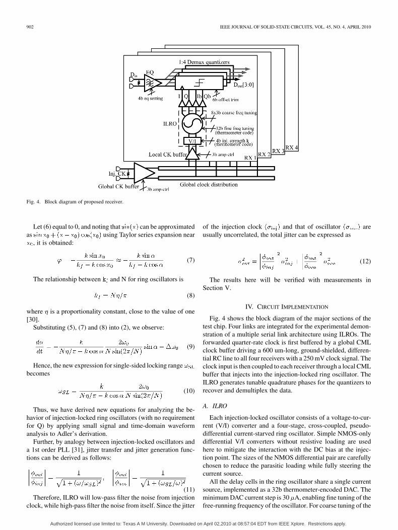
Fig. 4. Block diagram of proposed receiver.
Let (6) equal to 0, and noting that can be approximatedas using Taylor series expansion near
, it is obtained:
(7)
The relationship between and N for ring oscillators is
(8)
where is a proportionality constant, close to the value of one[30].
Substituting (5), (7) and (8) into (2), we observe:
(9)
Hence, the new expression for single-sided locking rangebecomes
(10)
Thus, we have derived new equations for analyzing the be-havior of injection-locked ring oscillators (with no requirementfor Q) by applying small signal and time-domain waveformanalysis to Adler’s derivation.
Further, by analogy between injection-locked oscillators anda 1st order PLL [31], jitter transfer and jitter generation func-tions can be derived as follows:
(11)Therefore, ILRO will low-pass filter the noise from injection
clock, while high-pass filter the noise from itself. Since the jitter
of the injection clock and that of oscillator areusually uncorrelated, the total jitter can be expressed as
(12)
The results here will be verified with measurements inSection V.
IV. CIRCUIT IMPLEMENTATION
Fig. 4 shows the block diagram of the major sections of thetest chip. Four links are integrated for the experimental demon-stration of a multiple serial link architecture using ILROs. Theforwarded quarter-rate clock is first buffered by a global CMLclock buffer driving a 600 um-long, ground-shielded, differen-tial RC line to all four receivers with a 250 mV clock signal. Theclock input is then coupled to each receiver through a local CMLbuffer that injects into the injection-locked ring oscillator. TheILRO generates tunable quadrature phases for the quantizers torecover and demultiplex the data.
A. ILRO
Each injection-locked oscillator consists of a voltage-to-cur-rent (V/I) converter and a four-stage, cross-coupled, pseudo-differential current-starved ring oscillator. Simple NMOS-onlydifferential V/I converters without resistive loading are usedhere to mitigate the interaction with the DC bias at the injec-tion point. The sizes of the NMOS differential pair are carefullychosen to reduce the parasitic loading while fully steering thecurrent source.
All the delay cells in the ring oscillator share a single currentsource, implemented as a 32b thermometer-encoded DAC. Theminimum DAC current step is 30 A, enabling fine tuning of thefree-running frequency of the oscillator. For coarse tuning of the
Authorized licensed use limited to: Texas A M University. Downloaded on April 02,2010 at 08:57:04 EDT from IEEE Xplore. Restrictions apply.

HU et al.: SERIAL LINK RECEIVER USING LOCAL INJECTION-LOCKED RING OSCILLATORS IN 90 nm CMOS 903
Fig. 5. Schematic of ILRO.
free-running VCO frequency, either the supply can be reducedor a 3b switched capacitor array can be utilized.
Injection-locking will cause adjacent time-interleaved phasesof the oscillator to be unevenly spaced. For example, the in-jection nodes CK135 and CK315 exhibit significant phaseasymmetry from the other six phases, as these nodes arethe summing nodes from the injection-locking interpolation.However, once the differential clocks are propagated to CK0and CK180, they are decoupled from the injection-point phaseasymmetry, and now exhibit conventional inverter loading anddelay. Hence, the four alternating phases (every two inverterstages) CK180, CK270, CK0, CK90 maintain adequate quadra-ture accuracy (less than 4.5 ), both in the simulated as well asin the experimental results. Each of the eight multi-phases isloaded with the same inverter buffering, to maintain the samecapacitive loading. Further phase symmetry is obtained byusing small cross-coupled inverters between complementaryphases, as well as using a 3b binary capacitor bank on eachoutput clock phase to individually trim the phase imbalancesthat arise due to process variations or layout mismatch. Inaddition, for a typical application (not implemented here), anoffline, static phase calibration of multiple, time-interleavedphases at reset time would be included to resolve maximumphase mismatch to several picoseconds [32], [33].
B. Linear Equalizer
The front-end receiver equalizer is the analog componentthat works at the highest frequency of all the receiver blocks.A source-degenerated, linear equalizer similar to [9] is imple-mented, as shown in Fig. 6(a). Its voltage gain can be written as
(13)
Fig. 6. (a) Schematic of RX EQ. (b) quantizer with offset control.
where , ,and output pole . Therefore, and C intro-duce a zero before the pole . If the output pole isalso designed to be larger than the zero, gain will be boostedbetween and the smaller one of and . By switchingthe value of the degenerated resistor , the DC gain will changeas shown in Fig. 7, resulting in an effective high-pass filteringeffect.
C. Other Building Blocks
Each quantizer of the 1:4 demuxplexing is implementedusing a two-stage sense amplifier [34] and SR latch, as shownin Fig. 6(b). A 6b binary current source can be injected to nodes
and in order to cancel the quantizer offset by current-im-balancing.
Authorized licensed use limited to: Texas A M University. Downloaded on April 02,2010 at 08:57:04 EDT from IEEE Xplore. Restrictions apply.

904 IEEE JOURNAL OF SOLID-STATE CIRCUITS, VOL. 45, NO. 4, APRIL 2010
Fig. 7. Simulated AC response of RX EQ under different settings.
Fig. 8. Die photo and layout screen capture.
V. EXPERIMENTAL RESULTS
The 1 mm test chip has been fabricated in a 90 nm, 1.2 VCMOS process and tested in a chip-on-board assembly. Asshown in Fig. 8, it integrates four receivers, the global clockdistribution network, a digital scan chain, test output buffers anda stand-alone ILRO for test purposes. Each receiver occupies0.0174 mm . Due to the limitation in pad area, only near-end(RX1) and far-end (RX4) I/Os are measured. In each receiver,the four-way, demultiplexed output data can be individuallyselected to drive the output pads.
A. ILRO
In this subsection, the analytical equations derived inSection III will be examined and compared with measurementdata. Note that the stage number and assumes .The ILRO can tune from 1.6 GHz to 2.6 GHz by coarse tuningits supply, while turning on all switches in the digital switchcapacitor bank can provide an additional 250–300 MHz fre-quency range. Hence, this large and fine tuning range can beused to compensate possible variations. Note that a shared,frequency-locked loop (not implemented in this work) initiatedat reset time, can be used at startup to calibrate and compensatefor initial oscillation frequency variations [35].
Fig. 9(a) shows both the measured deskew under different in-jection strength and the analytical model predicted from (9).In this measurement, the injection clock was kept constant at2.5 GHz and the current-DAC, fine tuning control was swept
Fig. 9. (a) Deskew of ILRO; (b) overlaid waveforms by sweeping phase set-tings (vertical scale � 25 mV/div, horizontal scale � 10 ps/div).
until the oscillator operated beyond its locking range. The mea-sured phase shift confirms the same deskew characteristics asthe simulated ILRO shown previously in Fig. 2(b). The mea-sured results also show that the ILRO can achieve greater than
linear deskew range. Fig. 9(b) plots the correspondingoutput waveforms of the ILRO, overlaid on oscilloscope, givingan intuitive viewpoint of the fine interpolation steps of ILRO.The measured injection-locking ranges for injection strength
0.03, 0.06, 0.09, and 0.12 are 65, 115, 167, and 203 MHz,respectively.
The jitter performance was measured by keeping the free-run-ning frequency fixed at round 2.5 GHz and sweeping the fre-quency of the injection clock. Fig. 10 shows that the jitter ofILRO will first get slightly worse as the frequency of injectionclock moves away from the free-running frequency, and thenget dramatically worse at the edge of locking range. By sub-stituting measured RMS jitters of injection clock and free-run-ning ring oscillator into (12), we can successfully predict thejitter degradation when the injection clock is near the free-run-ning frequency. This is because will reduce slightly due to
Authorized licensed use limited to: Texas A M University. Downloaded on April 02,2010 at 08:57:04 EDT from IEEE Xplore. Restrictions apply.

HU et al.: SERIAL LINK RECEIVER USING LOCAL INJECTION-LOCKED RING OSCILLATORS IN 90 nm CMOS 905
Fig. 10. Jitter performance of ILRO.
Fig. 11. Measured phase noise performance of ILRO.
the change of from (10), such that more noise of the oscil-lator will pass through to the output. At the edge of the lockingrange, the jitter worsens because the oscillator is on the cuspof losing phase lock. However, across the linear deskew range,the jitter stays sufficiently low (below 1.5 ps RMS jitter when
) such that the jitter degradation will not affect thenormal operation of the ILRO. Corresponding measurements ofthe phase noise shows a similar tendency in the performancedegradation, as shown in Fig. 11.
The 3 dB bandwidth at 0.03, 0.06, 0.09, and 0.12 are31, 55, 80, and 100 MHz, respectively, as shown in Fig. 12. Thismeasurement is done directly by injecting a stressed input clockwith 5% UI of sine jitter generated by a BertScope 12500B. Toverify the phase symmetry, quadrature output waveforms of theILRO are overlaid in Fig. 13. Measurement across the lineardeskew range shows a maximum I/Q phase and amplitude im-balance of 4.5 and 7 mV, respectively.
B. Entire Receiver
Experimental measurements are obtained from testing thefar-end receiver (RX4). RX4 exhibits the longest clock distri-bution distance among the four receivers, and therefore showsthe worse case performance of the four lanes. The results aremeasured from 6.4 Gb/s to 8 Gb/s with a 400 mV swing PRBS7 data sequence generated by the BertScope under two channelconditions: 1) chip-on-board bond-wire with a 4 cm PCB traceon the test board plus two SMA connectors and cables, and
Fig. 12. Measured jitter transfer of ILRO.
Fig. 13. Phase spacing when injecting 2.5 GHz clock: (a) � � 2.49 GHz,(b) � � 2.58 GHz (vertical scale � 25 mV/div, horizontal scale � 50 ps/div).
2) uses both 1) and an additional 10 cm of FR4 PCB trace. Theyare denoted as 4 cm trace and 14 cm trace in this paper, and ex-hibit approximately 1 dB and 5 dB loss at 4 GHz, respectively.
The receiver consumes 3.84 mW, 4.3 mW and 4.8 mW1 atinput data rates of 6.4 Gb/s, 7.2 Gb/s, and 8 Gb/s, respectively.Fig. 14 shows the breakdown of the power for the receiver. TheILRO occupies 23% of the total power consumption, which is
1We do not implement an on-chip regulator in this design. Supply noise wasmitigated by using large decoupling capacitors both on-chip and off-chip andtesting with an off-chip, precision digital voltage generator. Power of test buffersis not included.
Authorized licensed use limited to: Texas A M University. Downloaded on April 02,2010 at 08:57:04 EDT from IEEE Xplore. Restrictions apply.

906 IEEE JOURNAL OF SOLID-STATE CIRCUITS, VOL. 45, NO. 4, APRIL 2010
Fig. 14. Receiver power breakdown.
Fig. 15. Eye diagrams of recovered data under (a) 4 cm trace and (b) 14 cmtrace (input data rate� 7.2 Gb/s, vertical scale� 155 mV/div, horizontal scale� 111 ps/div).
about half the ratio of a phase rotator within a conventional linkreceiver, as in [9]. Therefore the clock related power is reducedto about 53% of the total receiver power.
Eye diagrams of one stream of recovered 1.8 Gb/s data fromthe 7.2 Gb/s input are shown in Fig. 15. There exists a slightlybimodal eye diagram when the 14 cm PCB trace is used. Due to asub-optimal design of the equalizer where the peak is placed 2lower than desired for this PCB Nyquist bandwidth, the channel
Fig. 16. BER measurements (a) by sweeping the delay in BERT and (b) bysweeping the phase setting of ILRO.
TABLE IPERFORMANCE SUMMARY
plus component assembly results in more loss and reflectionthan expected, such that the equalization is not enough to com-pensate for the channel losses at higher data rate. Fig. 16 plotsthe measured BER bathtub curves for the two channel condi-tions, with the measured performance summarized in Table I.Table II compares the performance with prior state-of-the-art,energy-efficient serial links.
VI. CONCLUSION
A four-lane, 6.4–7.2 Gb/s per link, parallel serial link receiverdesign has been presented. The proposed forwarded clock ar-
Authorized licensed use limited to: Texas A M University. Downloaded on April 02,2010 at 08:57:04 EDT from IEEE Xplore. Restrictions apply.

HU et al.: SERIAL LINK RECEIVER USING LOCAL INJECTION-LOCKED RING OSCILLATORS IN 90 nm CMOS 907
TABLE IICOMPARISON WITH RECENT DESIGNS
chitecture using ILROs allows the test chip to obtain full UIdeskew while achieving only 0.6 mW/Gb/s under moderatechannel losses. The use of ILROs also exhibits other bene-fits including inherent multiphase generation and large jittertransfer bandwidth. Methods to avoid the nonlinearity of ILROsare also discussed. Simple analytical equations are derived tounderstand both the injection locking and jitter performance ofILROs and are verified with experimental measurements. Themethods presented provide new insights into low power seriallink design for future multi-Gb/s I/O interfaces.
ACKNOWLEDGMENT
The authors would like to thank Brent Close, Charlie Zhongand Freeman Zhong of LSI, for generous support of lab andequipment measurement time, Intel for funding support, andMOSIS for help in chip fabrication.
REFERENCES
[1] M. Tremblay and S. Chaudhry, “A third-generation 65 nm 16-core32-thread plus 32-scout-thread CMT SPARC processor,” in IEEEISSCC Dig. Tech. Papers, Feb. 2008, pp. 82–83.
[2] S. Bell, B. Edwards, and J. Amann et al., “TILE64TM processor: A64-core SoC with mesh interconnect,” in IEEE ISSCC Dig. Tech. Pa-pers, Feb. 2008, pp. 88–89.
[3] S. Scott, D. Abts, J. Kim, and W. J. Dally, “The BlackWidow high-radix Clos network,” in Proc. ISCA ’06, Jun. 2006, pp. 16–28.
[4] HyperTransport I/O Technology Overview [Online]. Available: http://www.hypertransport.org/docs/wp/HT_Overview.pdf
[5] An Introduction to the Intel QuickPath Interconnect [Online]. Avail-able: www.intel.com/technology/quickpath/introduction.pdf
[6] L. Rodoni, G. von Buren, A. Huber, M. Schmatz, and H. Jackel, “A5.75 to 44 Gb/s quarter rate CDR with data rate selection in 90 nm bulkCMOS,” IEEE J. Solid-State Circuits, vol. 44, no. 7, pp. 1927–1941,July 2009.
[7] Y. Amamiya, S. Kaeriyama, and H. Noguchi et al., “A 40 Gb/s multi-data-rate CMOS transceiver chipset with SFI-5 interface for opticaltransmission systems,” in IEEE ISSCC Dig. Tech. Papers, Feb. 2009,pp. 358–359.
[8] F. O’Mahony, S. Shekhar, and M. Mansuri et al., “A 27 Gb/s for-warded-clock I/O receiver using an injection-locked LC-DCO in 45 nmCMOS,” in IEEE ISSCC Dig. Tech. Papers, Feb. 2008, pp. 452–453.
[9] J. Poulton, R. Palmer, and A. M. Fuller et al., “A 14-mW 6.25-Gb/stransceiver in 90-nm CMOS,” IEEE J. Solid-State Circuits, vol. 42, no.12, pp. 2745–2757, Dec. 2007.
[10] H. Lee, K.-Y. K. Chang, and J.-H. Chun et al., “A 16 Gb/s/link, 64GB/s bidirectional asymmetric memory interface,” IEEE J. Solid-StateCircuits, vol. 44, no. 4, pp. 1235–1247, Apr. 2009.
[11] M. Pozzoni, S. Erba, and P. Viola et al., “A multi-standard 1.5 to 10Gb/s latch-based 3-tap DFE receiver with a SSC tolerant CDR for serialbackplane communication,” IEEE J. Solid-State Circuits, vol. 44, no.4, pp. 1306–1315, Apr. 2009.
[12] L. Zhang, B. Ciftcioglu, M. Huang, and W. Hui, “Injection-lockedclocking: A new GHz clock distribution scheme,” in IEEE Proc. CICC,Sep. 2006, pp. 785–788.
[13] P. Chiang, W. J. Dally, and M.-J. E. Lee et al., “A 20 Gb/s 0.13 umCMOS serial link transmitter using an LC-PLL to directly drive theoutput multiplexer,” IEEE J. Solid-State Circuits, vol. 40, no. 4, pp.1004–1011, Apr. 2005.
[14] K. Hu, T. Jiang, J. Wang, F. O’Mahony, and P. Y. Chiang, “A0.6 mW/Gbps, 6.4-8.0 Gbps serial link receiver using local injec-tion-locked ring oscillators in 90 nm CMOS,” in Symp. VLSI CircuitsDig., Jun. 2009, pp. 46–47.
[15] R. Alder, “A study of locking phenomena in oscillators,” Proc. IRE,vol. 34, pp. 351–356, Jun. 1946, reprinted in Proc. IEEE, vol. 61, pp.1380–1385, Oct. 1973.
[16] L. J. Paciorek, “Injection locking of oscillators,” Proc. IEEE, vol. 53,no. 11, pp. 1723–1728, Nov. 1965.
[17] B. Razavi, “A study of injection locking and pulling in oscillators,”IEEE J. Solid-State Circuits, vol. 39, no. 9, pp. 1415–1424, Sep. 2004.
[18] N. Lanka, S. Patnaik, and R. Harjani, “Understanding the behavior ofinjection locked LC oscillators,” in IEEE Proc. CICC, Sep. 2007, pp.667–670.
[19] J. Jaussi, B. Casper, and M. Mansuri et al., “A 20 Gb/s embedded clocktransceiver in 90 nm CMOS,” in IEEE ISSCC Dig. Tech. Papers, Feb.2006, pp. 340–341.
[20] B. Casper, J. Jaussi, and F. O’Mahony et al., “A 20 Gb/s forwardedclock transceiver in 90 nm CMOS,” in IEEE ISSCC Dig. Tech. Papers,Feb. 2006, pp. 90–91.
[21] B. Casper and F. O’Mahony, “Clocking analysis, implementation andmeasurement techniques for high-speed data links—A tutorial,” IEEETrans. Circuits Syst. I, Reg. Papers, vol. 56, no. 1, pp. 17–39, Jan.2009.
[22] A. Agrawal, P. K. Hanumolu, and G.-Y. Wei, “A 8 � 5 Gb/s source-synchronous receiver with clock generator phase error correction,” inIEEE Proc. CICC, Sep. 2008, pp. 459–462.
[23] Z. Xu and K. L. Shepard, “Low-jitter active deskewing through injec-tion-locked resonant clocking,” in IEEE Proc. CICC, Sep. 2007, pp.9–12.
[24] M. Hossain and A. C. Carusone, “CMOS oscillators for clock distri-bution and injection-locked deskew,” IEEE J. Solid-State Circuits, vol.44, no. 8, pp. 2138–2153, Aug. 2009.
[25] T. H. Lee and A. Hajimiri, “Oscillator phase noise: A tutorial,” IEEEJ. Solid-State Circuits, vol. 35, no. 3, pp. 326–336, Mar. 2004.
[26] B. Razavi, RF Microelectronics. Englewood Cliffs, NJ: Pren-tice-Hall, 1998, ch. 7–8.
[27] X. Lai and J. Roychowdhury, “Analytical equations for predicting in-jection locking in LC and ring oscillators,” in IEEE Proc. CICC, Sep.2005, pp. 461–464.
[28] G. R. Gangasani and P. R. Kinget, “Time-domain model for injectionlocking in nonharmonic oscillators,” IEEE Trans. Circuits Syst. I, Reg.Papers, vol. 55, no. 6, pp. 1648–1658, July 2008.
[29] B. Razavi, “A study of phase noise in CMOS oscillators,” IEEE J.Solid-State Circuits, vol. 31, no. 3, pp. 331–343, March 1996.
[30] A. Hajimiri, S. Limotyrakis, and T. H. Lee, “Jitter and phase noisein ring oscillators,” IEEE J. Solid-State Circuits, vol. 34, no. 6, pp.790–804, June 1999.
[31] V. F. Kroupa, Phase Lock Loops and Frequency Synthesis. NewYork: Wiley, 2003, ch. 1.
[32] L. Lee, D. Weinlader, and C.-K. K. Yang, “A sub-10-ps multiphasesampling system using redundancy,” IEEE J. Solid-State Circuits, vol.41, no. 1, pp. 265–273, Jan. 2006.
[33] J. Wang, “Techniques for improving timing accuracy of multi-gigahertztrack/hold circuits,” M.S. thesis, Dept. Elect. Eng., Oregon State Univ.,Corvallis, OR, 2008.
[34] D. Schinkel, E. Mensink, E. Klumperink, E. van Tuijl, and B. Nauta,“A double-tail latch-type voltage sense amplifier with 18 ps setup+holdtime,” in IEEE ISSCC Dig. Tech. Papers, Feb. 2007, pp. 314–315.
[35] J. Kim and M. A. Horowitz, “Adaptive supply serial links with sub-1-Voperation and per-pin clock recovery,” IEEE J. Solid-State Circuits, vol.37, no. 11, pp. 1403–1413, Nov. 2002.
Authorized licensed use limited to: Texas A M University. Downloaded on April 02,2010 at 08:57:04 EDT from IEEE Xplore. Restrictions apply.

908 IEEE JOURNAL OF SOLID-STATE CIRCUITS, VOL. 45, NO. 4, APRIL 2010
Kangmin Hu (S’08) received the B.S. degree in elec-trical engineering from Shanghai Jiao Tong Univer-sity, Shanghai, China, in 2004 and the M.S. degree inmicroelectronics from Fudan University, Shanghai,China, in 2007. He is currently working toward thePh.D. degree in electrical engineering at Oregon StateUniversity, Corvallis, OR.
During the spring of 2007, he interned at IntelFlash Products Group in Shanghai, China. In 2009,he was a summer intern at Montage Technology,Shanghai, China. His current research interests
include system analysis and circuit design on low power multi-Gb/s wirelinetransceivers.
Tao Jiang (S’08) received the B.E. degree inelectronic information and engineering in 2004,and the M.S.E.E. degree in electronic science andtechnology in 2007, both from Tsinghua University,Beijing, China. He is currently working toward thePh.D. degree at Oregon State University, Corvallis,OR.
He was an intern at LSI Corporation, Milpitas, CA,from September to December 2008, where he was in-volved with the research on the high-speed ADC de-sign. His current technical and research interests in-
clude low-power, high-speed ADC and serial link design.
Jingguang Wang received the B.Sc. and M.Sc.degrees in microelectronics from Fudan University,Shanghai, China, in 2003 and 2006, respectively,and the M.Sc. degree in electronic engineering fromOregon State University, Corvallis, OR, in 2008.
From 2006 to 2007, he was an RF/Analog DesignEngineer with RDA microelectronics, Shanghai,China, where he worked on the satellite TV tunerdesign. During the summer of 2008, he internedat Telegent Systems in Sunnyvale, CA, designinga SAR ADC for tuner product. In 2008, he joined
Broadcom Corporation, Irvine, CA, working on the analog front-end forEthernet products.
Frank O’Mahony (S’99–M’03) received the B.S.,M.S., and Ph.D. degrees in electrical engineeringfrom Stanford University, Stanford, CA, in 1997,2000, and 2004, respectively. His doctoral researchfocused on resonant clock distribution techniquesfor high-performance microprocessors.
Since 2003, he has been with Intel’s Circuit Re-search Lab in Hillsboro, OR. His research interestsinclude high-speed and low-power data links, clockgeneration and distribution, and design techniquesfor low-noise, variation-tolerant clocking and sig-
naling circuits.Dr. O’Mahony received the 2003 Jack Kilby Award for Outstanding Student
Paper at ISSCC.
Patrick Yin Chiang (S’99–M’06) received theB.S. degree in electrical engineering and computersciences from the University of California, Berkeley,in 1998, and the M.S. and Ph.D. degrees in electricalengineering from Stanford University, Stanford, CA,in 2001 and 2007.
He is currently an Assistant Professor of electricaland computer engineering at Oregon State Univer-sity, Corvallis, OR. In 1998, he was with DatapathSystems (now LSI Logic), working on analog front-ends for DSL chipsets. In 2002, he was a research
intern at Velio Communications (now Rambus) working on 10 GHz clock syn-thesis architectures. In 2004, he was a consultant at startup Telegent Systems,evaluating low phase noise VCOs for CMOS mobile TV tuners. In 2006, hewas a Visiting NSF Postdoctoral Researcher at Tsinghua University, China, in-vestigating low-power, low-voltage RF transceivers. In summer 2007, he was aVisiting Professor at the Institute of Computing Technology, Chinese Academyof Sciences, where he collaborated on the design of multi-gigahertz ADCs andhigh-speed serial links. In December 2009, he was a Senior Visiting Researcherat Fudan University, Shanghai, China, researching mixed-signal circuits andsystems in the State Key Lab of ASIC and System. His interests are energy-ef-ficient VLSI interconnect and energy-constrained medical sensors.
Authorized licensed use limited to: Texas A M University. Downloaded on April 02,2010 at 08:57:04 EDT from IEEE Xplore. Restrictions apply.