ieee emc society distinguished lecturer...
TRANSCRIPT

IEEE EMC Society Distinguished Lecturer Seminar:IEEE EMC Society Distinguished Lecturer Seminar:IEEE EMC Society Distinguished Lecturer Seminar:Power Integrity of SiP (System In Package)
IEEE EMC Society Distinguished Lecturer Seminar:Power Integrity of SiP (System In Package)
July 21 2010July 21, 2010Joungho Kim at KAIST
joungho@ee kaist ac [email protected]://tera.kaist.ac.kr
Terahertz Interconnection and Package LaboratoryTERATerahertz Interconnection and Package Laboratory
1

Contents
I. Needs of SiP
II. Power Integrity of SiP
III PDN D i Ch ll i SiPIII. PDN Design Challenges in SiP
IV. Embedded decoupling capacitor and EBG structures
V. PDN Isolation in SiP design
VI PDN i li ff t Mi LNA d O AVI. PDN noise coupling effects on Mixer, LNA, and OpAmp
VI. SSN Free 3D Clock Distribution Network
VII. Power Integrity of TSV based 3D SiP
Terahertz Interconnection and Package LaboratoryTERATerahertz Interconnection and Package Laboratory
2
VIII. Conclusion
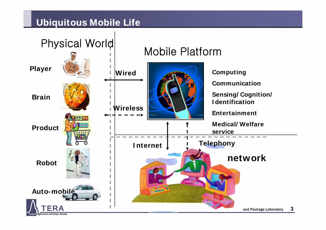
Ubiquitous Mobile LifeUbiquitous Mobile Life
Physical WorldMobile Platform
Player Wired Computing
Communication
BrainWireless
Sensing/Cognition/Identification
Entertainment
T l h
Product
Entertainment
Medical/Welfare service
network
Telephony Internet
Robot
Auto-mobile
Terahertz Interconnection and Package LaboratoryTERATerahertz Interconnection and Package Laboratory
3
Auto mobile

3D Convergence System In Package3D Convergence System In Package
3D Memory Multi-core3D MemoryStack
Multi-coreProcessor
RFTransmitter/Receiver
Filter Antenna
SRAMDRAMFlash
Receiver
Embeddedde-cap
TerminationResistor
EBGStructure
Terahertz Interconnection and Package LaboratoryTERATerahertz Interconnection and Package Laboratory
4

Advantages of SiP approachAdvantages of SiP approach
Small form factor
Fast time to market
Inhomogeneous device integration g g
Integration of passive devices, filters, and antenna
Suitable for RF mobile communication systems
Low cost
Terahertz Interconnection and Package LaboratoryTERATerahertz Interconnection and Package Laboratory
55

Power Supply Current PathPower Supply Current Path
Chip Ball Grid Array Package
Low Inductance Capacitor on PackageDiscrete Decoupling Capacitor on PCB
Bulk CapacitorBall Bonding
VRM Ground
Power
Wi B llP k PCBWireBonding
BallBonding
PackageP/G Network
PCBP/G NetworkChip VRMΔI
Decoupling CapacitorOn Package
Decoupling CapacitorOn PCB
Bulk CapacitorNear VRM
Decoupling CapacitorOn Chip
Low impedance path of current-flow at high frequency.
Screen out large inductance.
Terahertz Interconnection and Package LaboratoryTERATerahertz Interconnection and Package Laboratory
6

Simultaneous Switching Noise (SSN)Simultaneous Switching Noise (SSN)
ΔI=ΔI1+ ΔΙ2+ ΔIn
V=VCC+ΔV
ΔI1 ΔI2 ΔIn
ΔI=ΔI1+ ΔΙ2+ …ΔIn
L
Common Power Supply
H
L
H
L
H
L1 2 n
L
Parasitic Inductance(due to Pins, Bond-wire, etc.)
Common GroundChip
Simultaneous Switching Noise (SSN) : ΔV = LΔIΔt
Increase of Maximum Power (Current)
Increase of Clock Frequency
SSN caused by simultaneous switching output buffers
Terahertz Interconnection and Package LaboratoryTERATerahertz Interconnection and Package Laboratory
7

Problems caused by SSN
- Voltage margin reduction
- Logic failure
N i li t iti i it (RF d l i it )- Noise coupling to sensitive circuits (RF and analog circuits)
- Circuit reliability degradation (S/N, sensitivity)
- Signal integrity degradation ( eye, jitter)
El t ti di ti- Electromagnetic radiation
Terahertz Interconnection and Package LaboratoryTERATerahertz Interconnection and Package Laboratory
8

Inductive Impedance of PDN in SiPInductive Impedance of PDN in SiP
LPKG,wireLPKG,traceLPKG,via
LPCB,decap
SG
PKG,viaLPKG,ball
G
P
LP/G planeLPCB,via
S
LLtotlal = LPKG,wire+ LPKG,trace+ LPKG,via+ LPKG,ball+ LPCB,via+ LP/G plane+ LPCB,decap
Terahertz Interconnection and Package LaboratoryTERATerahertz Interconnection and Package Laboratory
9

Reduction of PDN Inductance
- Locate as close as possible
- Reduce length of interconnectg
- Wider, planar interconnect
- Ground/return current path as close as possible, minimal loop size
- Choose low ESL decoupling capacitorsChoose low ESL decoupling capacitors
- On chip decap > on-package decap > on-PCB decap
- Thinner PCB and package substrate
- Provide multiple paths (via pin wire decoupling capacitors)Provide multiple paths (via, pin, wire, decoupling capacitors)
- Choose advanced package
Terahertz Interconnection and Package LaboratoryTERATerahertz Interconnection and Package Laboratory
10- Cost balance needed

Power/Ground Network ImpedancePower/Ground Network Impedance
Actual
peda
nce
ActualImpedance
P/G
Imp
IdealImpedance
Frequency [log]kHz MHz GHz THz
Terahertz Interconnection and Package LaboratoryTERATerahertz Interconnection and Package Laboratory
11

Frequency Dependent Functions of Discrete Decoupling CapacitorFrequency Dependent Functions of Discrete Decoupling Capacitor
e
Chip Decoupling Capacitor
VRMjLjjLj ω<ω
mpe
danc
e
Power
Ground DECAPDECAP
VRMVRM C
LjC
Ljω
−ω<ω
−ω
Net
wor
k I
Capacitance given byDiscrete Decoupling Capacitors
Capacitance byPower/Ground Plane
r/G
roun
d N
Pow
er
Inductance byVRM or
Inductance given by• ESL of Discrete Capacitor Inductance by
Power/Ground Plane
MH GHzFrequency
ESL of Bulk Capacitor • Mount Pad• Power/Ground Traces• Power/Ground Via
Power/Ground Plane
KH
Terahertz Interconnection and Package LaboratoryTERATerahertz Interconnection and Package Laboratory
12
MHz GHzKHz
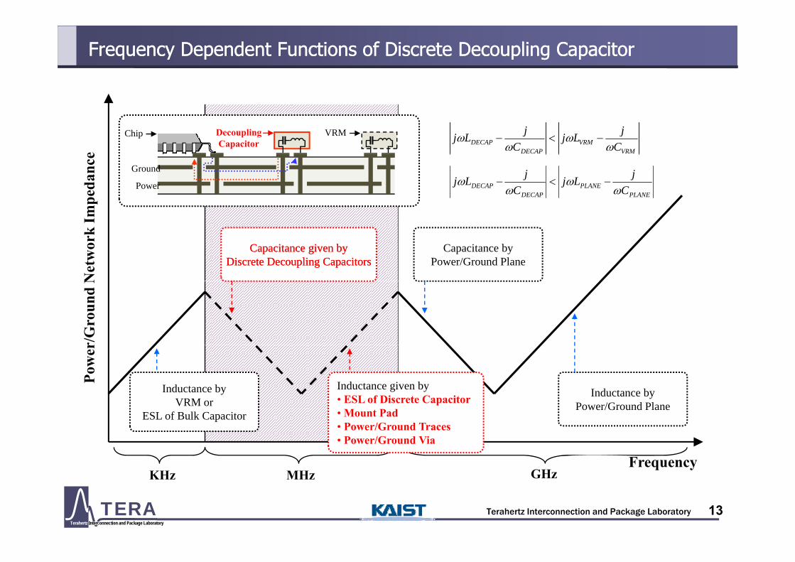
Frequency Dependent Functions of Discrete Decoupling CapacitorFrequency Dependent Functions of Discrete Decoupling Capacitor
e VRMVRM
DECAPDECAP C
jLjC
jLjω
ωω
ω −<−Chip Decoupling Capacitor
VRM
mpe
danc
e VC
PLANEPLANE
DECAPDECAP C
jLjC
jLjω
ωω
ω −<−Power
Ground
Net
wor
k I
Capacitance given byCapacitance given byDiscrete Decoupling CapacitorsDiscrete Decoupling Capacitors
Capacitance byPower/Ground Plane
r/G
roun
d N
Pow
er
Inductance byVRM or
Inductance given by• ESL of Discrete Capacitor Inductance by
Power/Ground Plane
MH GHzFrequency
ESL of Bulk Capacitor • Mount Pad• Power/Ground Traces• Power/Ground Via
Power/Ground Plane
KH
Terahertz Interconnection and Package LaboratoryTERATerahertz Interconnection and Package Laboratory
13
MHz GHzKHz

Good Power Distribution NetworkGood Power Distribution Network
Decoupling Capacitor
Battery
p
Voltage regulator
PowerPower plane on PCB
PackageDevice
Power trace on PCB
Wire-bond
Terahertz Interconnection and Package LaboratoryTERATerahertz Interconnection and Package Laboratory
14
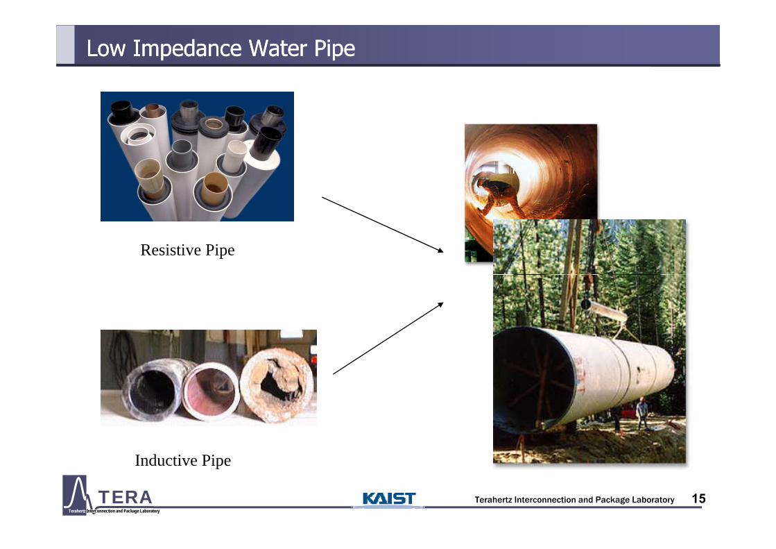
Low Impedance Water PipeLow Impedance Water Pipe
Resistive Pipe
Inductive Pipe
Terahertz Interconnection and Package LaboratoryTERATerahertz Interconnection and Package Laboratory
15
Inductive Pipe

What happens if power distribution network is bad?What happens if power distribution network is bad?
Terahertz Interconnection and Package LaboratoryTERATerahertz Interconnection and Package Laboratory
16
What happens if power distribution network is Good?What happens if power distribution network is Good?
Terahertz Interconnection and Package LaboratoryTERATerahertz Interconnection and Package Laboratory
17

Impedance Property of Chip-Package-PCB Hierarchical PDNImpedance Property of Chip-Package-PCB Hierarchical PDNth
m) Interaction Interaction
nce
(Log
ari
Impe
dan
Frequency (Logarithm)10MHz 100MHz 1GHz 10GHz
Advantage and application of PDN analysis in frequency domainAdvantage and application of PDN analysis in frequency domain
- Intuitive analysis
- Easy to control impedance property
Need for hierarchical PDN simulation
Terahertz Interconnection and Package LaboratoryTERATerahertz Interconnection and Package Laboratory
18- Interactions between different level PDNs generate high impedance peak.
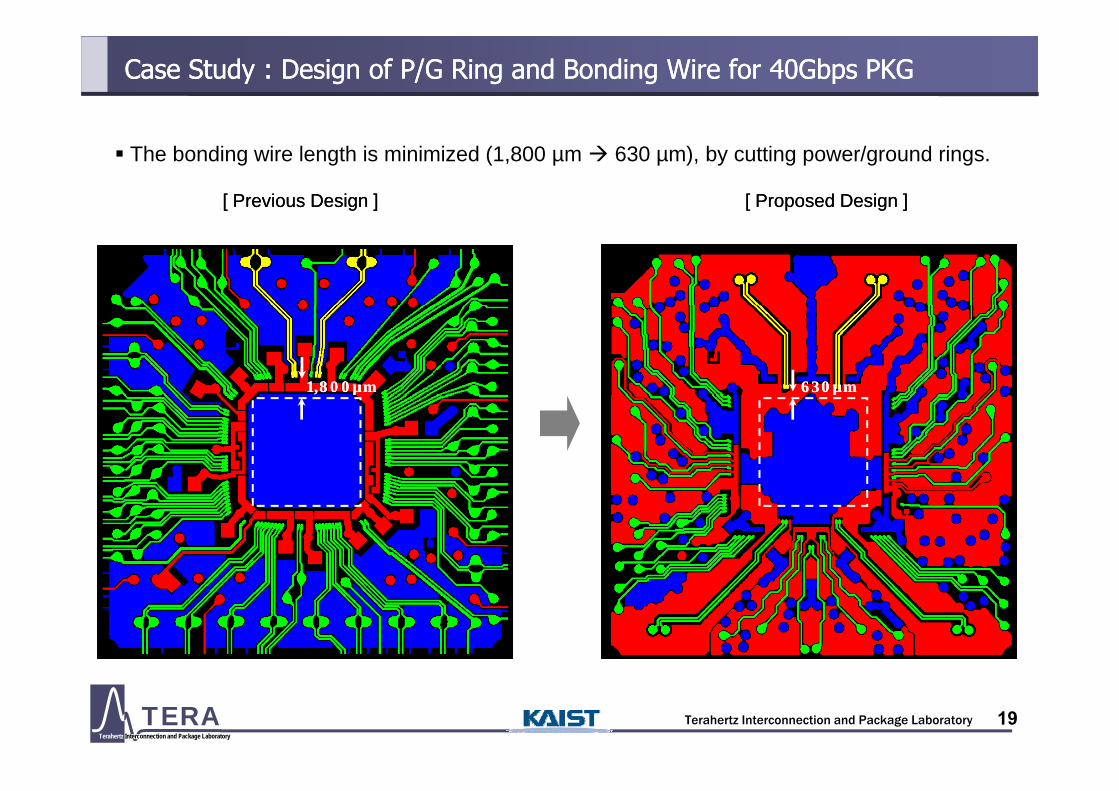
Case Study : Design of P/G Ring and Bonding Wire for 40Gbps PKG Case Study : Design of P/G Ring and Bonding Wire for 40Gbps PKG
The bonding wire length is minimized (1,800 µm 630 µm), by cutting power/ground rings.
[ Previous Design ][ Previous Design ] [ Proposed Design ][ Proposed Design ]
630µm630µm1,800µm1,800µm
Terahertz Interconnection and Package LaboratoryTERATerahertz Interconnection and Package Laboratory
19
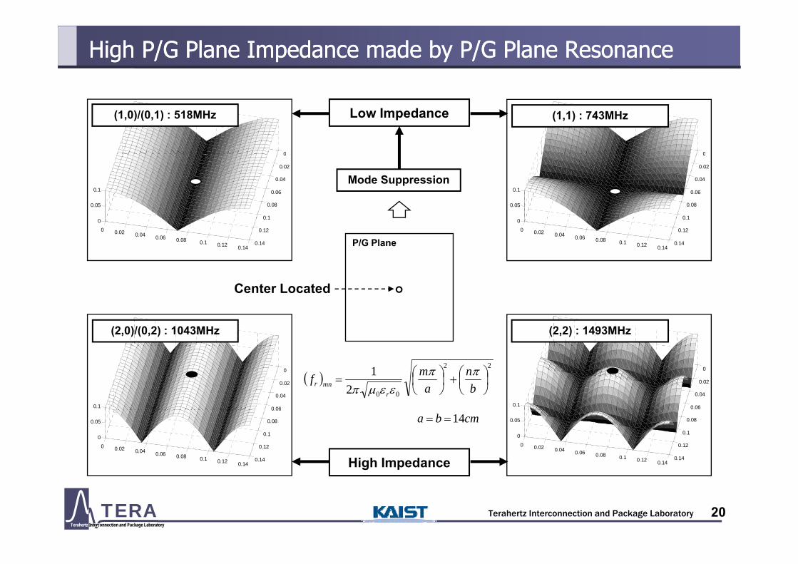
High P/G Plane Impedance made by P/G Plane ResonanceHigh P/G Plane Impedance made by P/G Plane Resonance
00
(1,0)/(0,1) : 518MHz (1,1) : 743MHzLow Impedance
0
0.02
0.04
0.06
0.08
0 1
0.05
0.1
0
0.02
0.04
0.06
0.08
0 1
0.05
0.1Mode Suppression
0.1
0.12
0.14
0 0.02 0.04 0.06 0.08 0.1 0.12 0.14
00.1
0.12
0.14
0 0.02 0.04 0.06 0.08 0.1 0.12 0.14
0
P/G Plane
Center Located
(2,0)/(0,2) : 1043MHz (2,2) : 1493MHz
0
0.02
0.04
0.060.1
0
0.02
0.04
0.060.1
( )22
0021
⎟⎠⎞
⎜⎝⎛+⎟
⎠⎞
⎜⎝⎛=
bn
amf
rmnr
ππεεμπ
0.08
0.1
0.12
0.14
0 0.02 0.04 0.06 0.08 0.1 0.12 0.14
0
0.05
0.06
0.08
0.1
0.12
0.14
0 0.02 0.04 0.06 0.08 0.1 0.12 0.14
0
0.05
High Impedance
cmba 14==
Terahertz Interconnection and Package LaboratoryTERATerahertz Interconnection and Package Laboratory
20

Spectrum Analyzer Measurement of P/G Plane Edge Radiation Spectrum Analyzer Measurement of P/G Plane Edge Radiation
500 MHz CLK10B
m] 0
100
TV2 SA Measurement TV2 P/G Plane Impedance
1478
-10
PP
G) [
dB
10
100 P/G
Pla
3rd- 30
n (S
A-P 1
ane Imp0.1
- 50
Rad
iatio
edance
0.01
(7cm 7cm)TV2
- 70
Edg
e R [Ω
]
(7cm,7cm)
14cm
Frequency [GHz]
0 0.5 1 1.5 2 2.5 3
Frequency [GHz] 14cm
Short Via
Terahertz Interconnection and Package LaboratoryTERATerahertz Interconnection and Package Laboratory
21
q y [ ]q y [ ]

plane cavity resonance modes
Power/Ground Network Impedance Power/Ground Network Impedance
20l |Z | (2,0)
plane cavity resonance modes
20log|ZPDN|
(1/4,0)(1,0)
(1,1)(2,0)
Parallel circuit resonance
PKG-level PDN
(1/4,0)-20dB/dec
lines Chip-level PDN
Cdecap2L decap2
Cdecap1
ωLTotal_Loop3
ωLTotal_Loop1
ωLTotal_Loop2
Series circuit resonance20dB/dec
plane cavity resonance modes
20dB/dec lines
Terahertz Interconnection and Package LaboratoryTERATerahertz Interconnection and Package Laboratory
22log f
plane cavity resonance modes
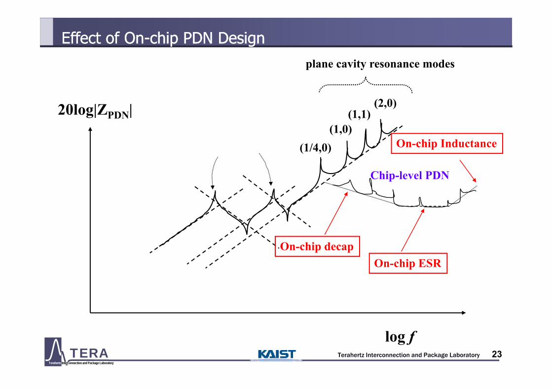
Effect of On-chip PDN DesignEffect of On-chip PDN Design
20l |Z | (2,0)
plane cavity resonance modes
20log|ZPDN|
(1/4,0)(1,0)
(1,1)(2,0)
On-chip Inductance(1/4,0)
Chip-level PDN
On-chip decapOn-chip ESR
Terahertz Interconnection and Package LaboratoryTERATerahertz Interconnection and Package Laboratory
23log f
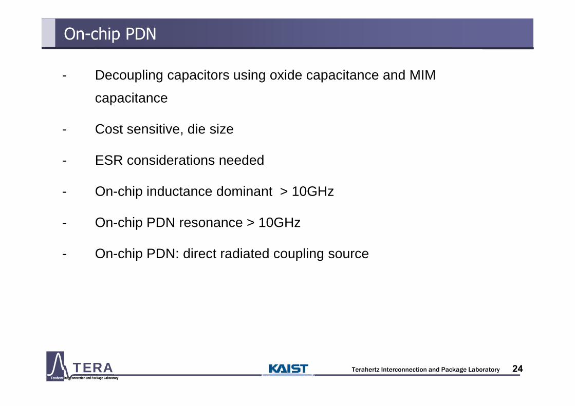
On-chip PDN
- Decoupling capacitors using oxide capacitance and MIM
capacitance
- Cost sensitive, die size
ESR id ti d d- ESR considerations needed
- On-chip inductance dominant > 10GHz
- On-chip PDN resonance > 10GHz
O hi PDN di t di t d li- On-chip PDN: direct radiated coupling source
Terahertz Interconnection and Package LaboratoryTERATerahertz Interconnection and Package Laboratory
24

Motivation –Cross-sectional View of Embedded Film CapacitorMotivation –Cross-sectional View of Embedded Film Capacitor
1 Removal of SMD Passive Componen
GND to Chip VDD to Chip
1. Removal of SMD Passive Componen(Enhanced Routibility)
Embedded Film Capacitor
2. Short Via Length(Low Via Inductance)
3. Small Thickness(Low Inductance)High Dielectric Material
Terahertz Interconnection and Package LaboratoryTERATerahertz Interconnection and Package Laboratory
2525
g(High Capacitance)

Fabricated Test Vehicles (with Thin Film Embedded Capacitor)Fabricated Test Vehicles (with Thin Film Embedded Capacitor)
A
VehicleCode Dielectric Thickness Dielectric Constant (DK)
50 μm 4.6
Capacitance/cm2
81.46 pF
Total Capacitance(5cm x 5cm with 2 pairs)
4.07 nF
B
C
25 μm
12 μm
4.6
4.6
162.91 pF
339.40 pF
8.15 nF
16.97 nF
D
E
10 μm
10 μm
16
25
1416.64 pF
2213.50 pF
70.83 nF
110.68 nF
25μm50μm 12μm
“A” with x50 “A” with x100 “A” with x500 “B” with x500 “C” with x500
Terahertz Interconnection and Package LaboratoryTERATerahertz Interconnection and Package Laboratory
26
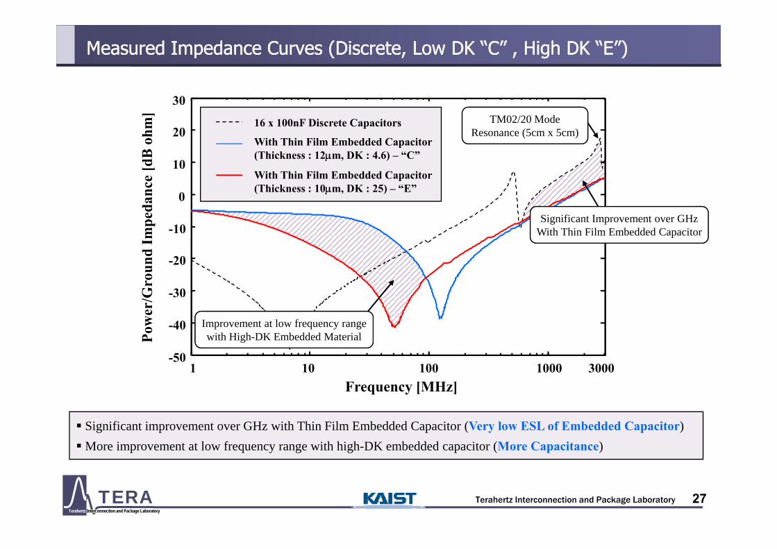
Measured Impedance Curves (Discrete, Low DK “C” , High DK “E”)Measured Impedance Curves (Discrete, Low DK “C” , High DK “E”)
20
30
B o
hm]
With Thin Film Embedded Capacitor
16 x 100nF Discrete Capacitors TM02/20 ModeResonance (5cm x 5cm)
0
10da
nce
[dB (Thickness : 12μm, DK : 4.6) – “C”
With Thin Film Embedded Capacitor(Thickness : 10μm, DK : 25) – “E”
-20
-10
ound
Impe Significant Improvement over GHz
With Thin Film Embedded Capacitor
-40
-30
Pow
er/G
ro
Improvement at low frequency rangewith High DK Embedded Material
-501 10 100 1000 3000
Frequency [MHz]
P with High-DK Embedded Material
Significant improvement over GHz with Thin Film Embedded Capacitor (Very low ESL of Embedded Capacitor)More improvement at low frequency range with high-DK embedded capacitor (More Capacitance)
Terahertz Interconnection and Package LaboratoryTERATerahertz Interconnection and Package Laboratory
27

Measured SSN (No De-Cap. Vs. Discrete De-Cap.)Measured SSN (No De-Cap. Vs. Discrete De-Cap.)
3.5
SSN
[V]
Vp-p : 370.2 mV
No Decoupling Capacitor
3.1
3.3M
easu
red
S
0 4 8 12 16 20Time [nsec]
M]
3 3
3.5
ed S
SN [V
]
Vp-p : 123.8 mV
16 x 100nF Discrete Capacitors High-frequency harmonic wasamplified with discrete capacitors
3.1
3.3
Mea
sure
0 4 8 12 16 20Time [nsec]
High frequency harmonic was amplified with discrete decoupling capacitors (as expected with impedance curve)
Terahertz Interconnection and Package LaboratoryTERATerahertz Interconnection and Package Laboratory
28

Measured SSN (Discrete, Low DK “C” , High DK “E”)Measured SSN (Discrete, Low DK “C” , High DK “E”)
3.5
SSN
[V] With Thin Film Embedded Capacitor
(Thickness : 12μm, DK : 4.6) – “C”Low-Frequency Harmonic was appeared
with Low DK Embedded Capacitor
3.1
3.3M
easu
red
S
Vp-p : 49.4 mV
0 4 8 12 16 20Time [nsec]
M]
3 3
3.5
ed S
SN [V
] With Thin Film Embedded Capacitor(Thickness : 10μm, DK : 25) – “E”
3.1
3.3
Mea
sure
Vp-p : 10.6 mV
SSN was almost suppressed with High-DK thin film embedded capacitor
0 4 8 12 16 20Time [nsec]
Terahertz Interconnection and Package LaboratoryTERATerahertz Interconnection and Package Laboratory
29

PDN Design Methods
- Frequency dependent capacitance and inductance control
- Increase of decoupling Capacitance depending frequency range- Increase of decoupling Capacitance depending frequency range
(on-chip, on-package, on-PCB, lumped, embedded)
- Decrease of Inductance (line, plane, via, wire, bonds, decoupling
capacitors )
- Control resonances (lumped, planar cavity, on-chip, inter-level):
avoid overlap with clock and harmonic frequencies
- Control ESR to reduce peak resonance impedance
- Evaluate dc ESR for dc voltage drop estimation
Terahertz Interconnection and Package LaboratoryTERATerahertz Interconnection and Package Laboratory
30

Proposed Modeling Method for Chip-Package-PCB Hierarchical PDNProposed Modeling Method for Chip-Package-PCB Hierarchical PDNx
f
y
f
Bond-wire4
1
Chip-level PDN1
8
Chip-level PDN
Package le el PDN2 P k l l
Bond-wire4
1
Fringing Field
9
Fringing Field 8
Package-level PDN
BallInter-level Coupling
75
2 Package-level PDN2
Fringing
9
9
PCB-level PDNVia
3
Vi
6
Inter-level
7
CouplingBall
5
Field
GroundPower
S t tiPCB-level
Via6
Coupling
Considering all parts in hierarchical PDN and merging them into one using
Ground Segmentation Method
PDN3
Terahertz Interconnection and Package LaboratoryTERATerahertz Interconnection and Package Laboratory
31
segmentation method

Analysis of Impedance of Test Vehicle at Package SideAnalysis of Impedance of Test Vehicle at Package SidePCB Mode (1 0)&(0 1)
PKG Mode (1 0)&(0 1)
PKG Mode (2 1)&(1 2)
100
(1,0)&(0,1)
PCB Mode (2,0)&(0,2)
PCB Mode (2,1)&(1,2)
(1,0)&(0,1)
PKG Mode (1,1)&(1,1)
PKG Mode
(2,1)&(1,2)
Adjacent PKG&Chip Effect
100
hm)
C kCPkg+CInt+CChip
PKG Mode (2,0)&(0,2)
10
edan
ce (o
h
CPkg+CIntCPkg
CPCB+CPkg+CInt+CChipLPkg+Via
1Impe
LChip+BondwireLPkg+Via+LInt//Ball
LPCB+Via+LPkg+Via+LInt//Ball
0.1
LPCB+Via LPkg+Via LInt//Ball
Frequency (GHz)0.1 1 10 20
A quite complicated impedance characteristic composed of chip-package-PCB
Terahertz Interconnection and Package LaboratoryTERATerahertz Interconnection and Package Laboratory
32
qu te co p cated peda ce c a acte st c co posed o c p pac age Chierarchical PDN is fully analyzed.

Verification of Proposed Modeling Method (Corner on Chip)Verification of Proposed Modeling Method (Corner on Chip)1000
100
1000MeasurementProposed Model
Chip (1,0)&(0,1)
Chip
ce (o
hm)
100
10
CPkg+CInt+CChip CPkg+CChip LPkg+Via+Bondwire+LChip
LChipCChip
Package
Impe
danc 10
1
LPCB+Via+LPkg+Via+Bondwire+LInt//Ball+LChip
LPkg+Via+Bondwire+LInt//Ball+LChip
C C C C
PCB
1 CPCB+CPkg+CInt+CChip
0.10.1 1 10 20
Frequency (GHz)The impedances at corner probe pad on chip
Frequency : 100MHz to 20GHz
5 high impedance peaks
4 peaks interactions
Terahertz Interconnection and Package LaboratoryTERATerahertz Interconnection and Package Laboratory
33
p
1 peak mode resonance of chip

Need for Estimation of High Impedance Peak in Hierarchical PDNNeed for Estimation of High Impedance Peak in Hierarchical PDN
Hi h i d i hi hi l PDN f i i bl f f d d i
EMIPower/Ground Noise
High impedances in hierarchical PDN from interactions generate problems of system performance degradation.
current
nce
VSSN=ZPDN × ICircuit
Impe
dan
Signal Degradation
RF /Analog
RF SensitivityFrequency
Digital
RF /Analog
Terahertz Interconnection and Package LaboratoryTERATerahertz Interconnection and Package Laboratory
34
A precise simulation and analysis of hierarchical PDN is needed.

PDN Noise Coupling Paths in chip and package
- Adjacent interconnections: line, pin, wire
- Via and planesp
- Conductive substrates
- Common power line, plane
- Common decoupling capacitorsCommon decoupling capacitors
- Common return current paths
- Isolation techniques needed: Cost, size increase
Terahertz Interconnection and Package LaboratoryTERATerahertz Interconnection and Package Laboratory
35
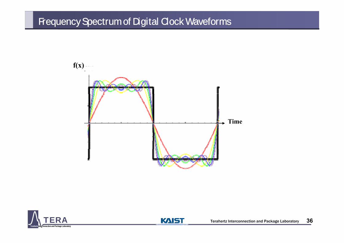
Frequency Spectrum of Digital Clock WaveformsFrequency Spectrum of Digital Clock Waveforms
f(x)f(x)
TimeTime
Terahertz Interconnection and Package LaboratoryTERATerahertz Interconnection and Package Laboratory
36

Waveform and Spectrum of Clock SignalWaveform and Spectrum of Clock Signal
100
150
0
20
100MHz200MHzFundamental : 100MHzOdd harmonicsEven harmonics
Fundamental : 200MHz
0
50
tude
(mV) 10ns
-20
er [d
Bm
]5ns
-100
-50
Mag
ni
-60
-40
Pow
e0 5 10 15 20-200
-150
Time (ns)0 500 1000 1500 2000 2500 3000
-80
Frequency [MHz]
100MHz200MHz
Terahertz Interconnection and Package LaboratoryTERATerahertz Interconnection and Package Laboratory
37
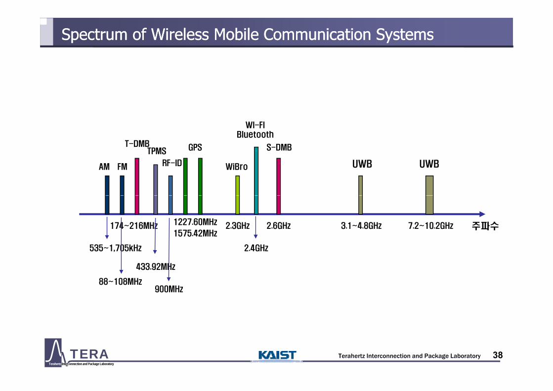
Spectrum of Wireless Mobile Communication SystemsSpectrum of Wireless Mobile Communication Systems
S-DMBT-DMB GPS
WI-FIBluetooth
TPMS
AM FM WiBro UWB UWB
TPMS
RF-ID
주파수174~216MHz 2.6GHz1227.60MHz
1575.42MHz2.3GHz 3.1~4.8GHz 7.2~10.2GHz
535~1,705kHz 2.4GHz
433.92MHz
88~108MHz900MHz
88 108MHz
Terahertz Interconnection and Package LaboratoryTERATerahertz Interconnection and Package Laboratory
38

Setup for AnalysisSetup for Analysis
Pulse Pattern Generator (PPG)
LO Signal
Observation Factors : 1. Transfer Impedance ( 1 , 2 ) 2. Noise Coupling Ratio ( 1 , 3 )3 Output Waveform ( 3 )
이미지를 표시할 수 없습니다 . 컴퓨터 메모리가 부족하여 이미지를 열 수 없거나 이미지가 손상되었습니다 . 컴퓨터를 다시 시작한 후 파일을 다시 여십시오 . 여전히 빨간색 x가 나타나면 이미지를 삭제한 다음 다시 삽입해야 합니다 .
• LO Frequency : 915.5MHz• LO Voltage : 400mV Pulse
LO Signal 3. Output Waveform ( 3 )
Output SignalPort2Port3
• Frequency : 500kHz• Power : -2dBm• Voltage : 250mV• Voltage Gain : 12dB
p g
Port1
Combine
Signal Generator (SG)
Balun
DC 2.5V• Frequency : 915MHz
14
RF Signal
r
• Frequency : 40kHz , 150MHz, 900MHz• Voltage : 80mV Pulse
P/G Noise
Balun• Power : -14dBm • Voltage : 60mV Sine Wave
Terahertz Interconnection and Package LaboratoryTERATerahertz Interconnection and Package Laboratory
3939/41

Basic Performance of Designed MixerBasic Performance of Designed Mixer
VDD
Double Balanced Mixer
Out+ Out-TSMC 0.25um Process
Target Frequency : 860 ~ 960 MHz
LO + LO +
Gain : 10 ~ 12 dB
P1dB : - 5dBm
RF Isolation : -30dBLO -
RF+
RF Isolation : -30dB
LO Isolation : -25dB
Direct Conversion Frequency : 500kHz
biasRF-
500kHz
Terahertz Interconnection and Package LaboratoryTERATerahertz Interconnection and Package Laboratory
40

On-chip Decap. Effect : Transfer Impedance ( Simulation )On-chip Decap. Effect : Transfer Impedance ( Simulation )
900MHz900MHz(1,0)
(1,1)(λ/4)
Without On-Chip Decap. VS With On-Chip Decap.
20
30
dB )
900MHz900MHz(0,1)
( , )
0
10
20
peda
nce
( d
Wirebond+On-chip Decap. Capacitance
-20
-10
ansf
er Im
p
On-chip Decap Effect (112pF).
-40
-30Without On-chip decap.With On-chip decap.
Tra
10M 100M 1GFrequency ( Hz )
• When on-chip decoupling capacitor is designed , transfer impedance decreases more than the case without on-chip decoupling capacitor over 600MHz
- > Transfer impedance decreases when design on-chip decoupling capacitor in 900MHz.
Terahertz Interconnection and Package LaboratoryTERATerahertz Interconnection and Package Laboratory
41
s e ped ce dec e ses w e des g o c p decoup g c p c o 900 .
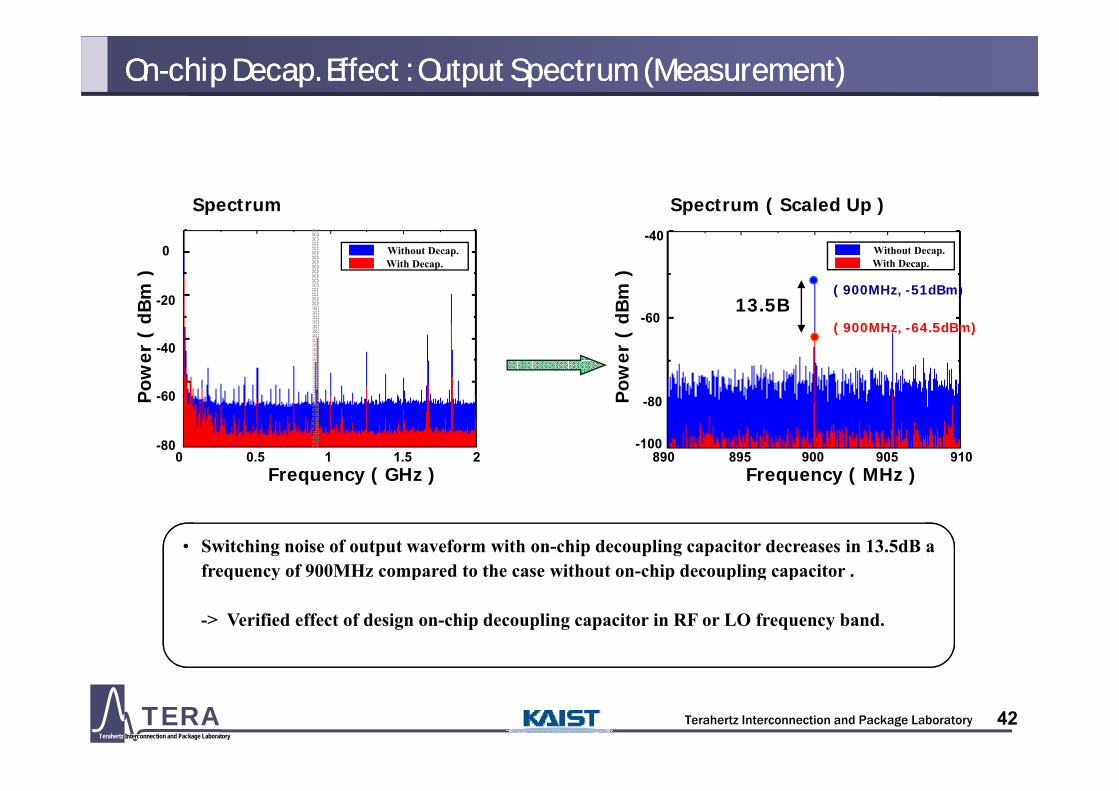
On-chip Decap. Effect : Output Spectrum (Measurement)On-chip Decap. Effect : Output Spectrum (Measurement)
Spectrum Spectrum ( Scaled Up )
13 5B( 900MHz, -51dBm)
Bm
)
Bm
)
-20
0-40
Without Decap.With Decap.
Without Decap.With Decap.
13.5B( 900MHz, -64.5dBm)
Pow
er (
dB
Pow
er (
dB
60
-40
-60
Frequency ( MHz )
P
Frequency ( GHz )
P
0 0.5 1 1.5 2-80
-60 -80
-100890 895 900 905 910
• Switching noise of output waveform with on-chip decoupling capacitor decreases in 13.5dB a frequency of 900MHz compared to the case without on-chip decoupling capacitor .frequency of 900MHz compared to the case without on chip decoupling capacitor .
-> Verified effect of design on-chip decoupling capacitor in RF or LO frequency band.
Terahertz Interconnection and Package LaboratoryTERATerahertz Interconnection and Package Laboratory
42

Off-chip Decap. Effect : Transfer Impedance (Simulation)Off-chip Decap. Effect : Transfer Impedance (Simulation)
150MHz
Without Off-Chip Decap. VS With Off-Chip Decap.
dB )
20
30
Off-chip Decap.
Off-Chip Capacitor :
L1= 540pH C1=101nF R1 =17mΩpeda
nce
( d10
20 p pEffect
L1= 540pH , C1=101nF , R1 =17mΩ
ansf
er Im
p
-10
0
Capacitance InductanceTra
-30
-20Without Off-chip decap.With Off-chip decap.
10k 100k 1M 10M 100M 1GFrequency ( Hz )
• When additional off-chip decoupling capacitor is designed , transfer impedance decreases more than the case without additional off-chip decoupling capacitor from 2MHz to 200MHz
Terahertz Interconnection and Package LaboratoryTERATerahertz Interconnection and Package Laboratory
43
- > Transfer impedance decreases when design on-chip decoupling capacitor in 150MHz.
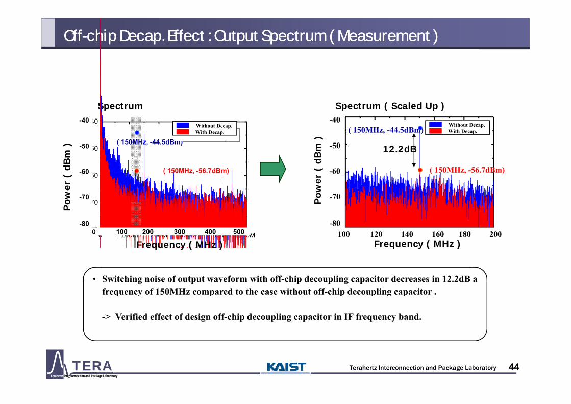
Off-chip Decap. Effect : Output Spectrum ( Measurement )Off-chip Decap. Effect : Output Spectrum ( Measurement )
Spectrum Spectrum ( Scaled Up )
-50
-40
Without Decap. With Decap.( 150MHz, -44.5dBm)
( 150MHz, -44.5dBm)
p p ( p )
Bm
)
m ) -50
-40
12.2dB-50
-40Without Decap.With Decap.
Without Decap.With Decap.
70
-60
( 150MHz, -56.7dBm)
Pow
er (
dB
ower
( d
Bm
-60
-70
( 150MHz, -56.7dBm)-60
-70
0 100M 200M 300M 400M 500M-80
-70
Frequency ( MHz )
P
Frequency ( MHz )
Po
100 200 300 400 500 120 140 160 180 200-80
100-80
0
q y ( )eque cy ( )
• Switching noise of output waveform with off-chip decoupling capacitor decreases in 12.2dB a frequency of 150MHz compared to the case without off-chip decoupling capacitor .frequency of 150MHz compared to the case without off chip decoupling capacitor .
-> Verified effect of design off-chip decoupling capacitor in IF frequency band.
Terahertz Interconnection and Package LaboratoryTERATerahertz Interconnection and Package Laboratory
44
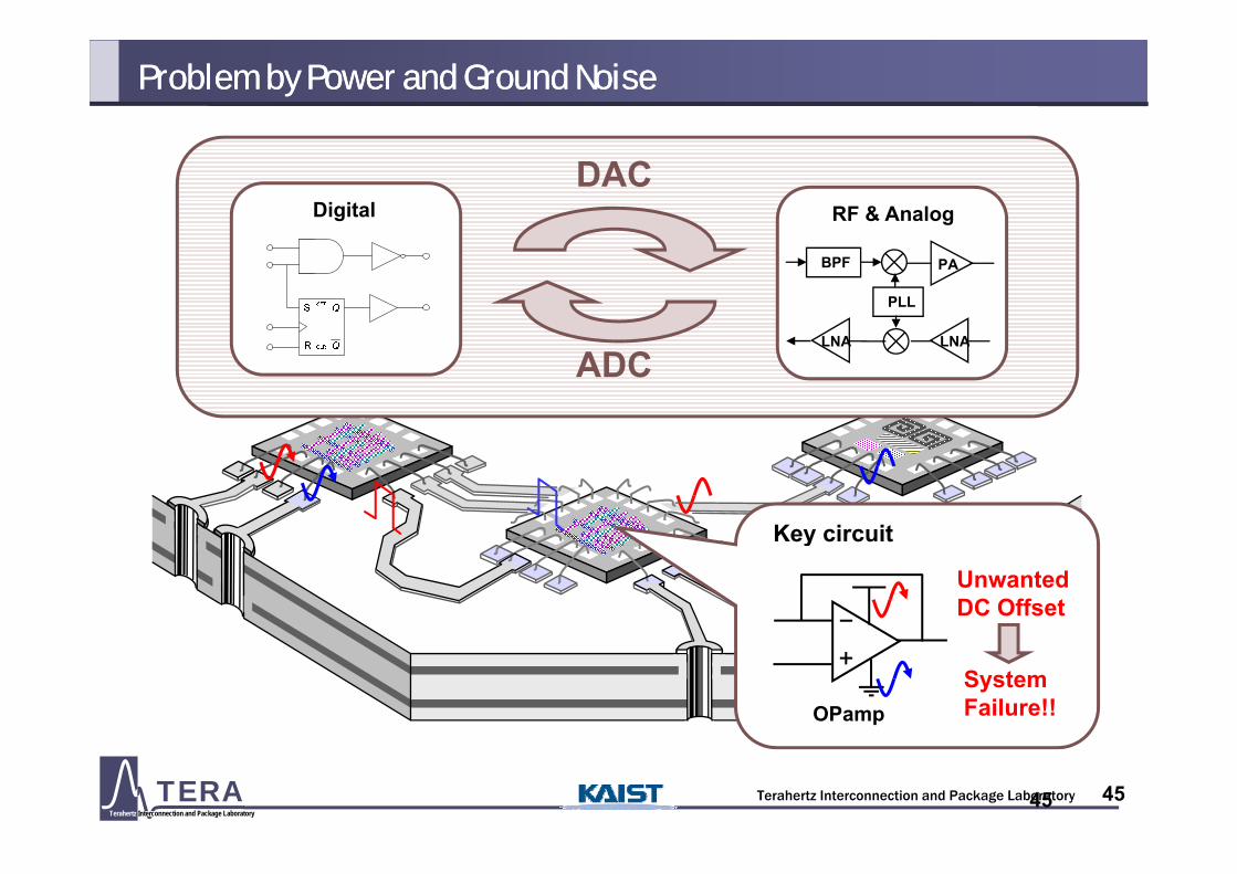
Problem by Power and Ground NoiseProblem by Power and Ground Noise
Digital RF & AnalogDAC
PA
LNA
PLL
BPF
LNA LNALNA
ADC
Key circuitKey circuit
Unwanted DC Offset
SystemFailure!!OPamp
Terahertz Interconnection and Package LaboratoryTERATerahertz Interconnection and Package Laboratory
4545

DC Output Offset with Proposed and Conventional AnalysisDC Output Offset with Proposed and Conventional Analysis
PDigital OP amp
P
DC Output Offset with Conventional Analysis
DigitalP
OP ampP
DC Output Offset with Proposed Analysis
100mV 100mV 100mV
60
_+
G GG
BondingWire
_+
G
Package PDN
ChipPDN
50
t (m
V)
Conventional analysisProposed analysis
30
40
utp
ut
Off
se
10
20DC
O
0 0.2 0.4 0.6 0.8 1 1.2 1.4 1.6 1.8 20
Frequency (GHz)C id bl Di i i b DC O Off
Terahertz Interconnection and Package LaboratoryTERATerahertz Interconnection and Package Laboratory
46
Considerable Distinction between DC Output Offsetwith and without Consideration of PDN
SSN Sensitive Circuits in IC
- VCO: Voltage Controlled Oscillator
- LNA: Low Noise Amplifier
PLL Ph L k d L- PLL: Phase Locked Loop
- ADC: Analog to Digital Converter
- DAC: Digital to Analog Converter
Terahertz Interconnection and Package LaboratoryTERATerahertz Interconnection and Package Laboratory
47
SSN Isolation Methods
- DecouplingDecoupling
- Filtering
- Slot
- SplitSplit
- Shielding
- EBG strictures
- Separated power supply/decoupling/return current pathSeparated power supply/decoupling/return current path
- Separated interconnections: lines, pins, pads, vias
- Separated planes, layers
- Increased separation distance
Terahertz Interconnection and Package LaboratoryTERATerahertz Interconnection and Package Laboratory
48
- Increased separation distance

PDN Noise Isolation MethodsPDN Noise Isolation Methods
Chip
Digital PDN Analog/RF PDN
PCBPackage
Ch
A
B
Chip Level Package/PCB LevelA Bp- Split On-chip Metal PDN Bus- Guard Ring (P+/ N+/ Deep-Nwell type)- On-chip Decoupling Capacitor
Internal Voltage Regulator
g- Split Power/Ground Planes- On-Package/PCB Decoupling Capacitor
(Discrete type, Embedded type)Electromagnetic Band Gap (EBG)- Internal Voltage Regulator - Electromagnetic Band Gap (EBG)
Frequency dependency of noise isolationZ21 l i i th f d i
Terahertz Interconnection and Package LaboratoryTERATerahertz Interconnection and Package Laboratory
49
Z21 analysis in the frequency domain
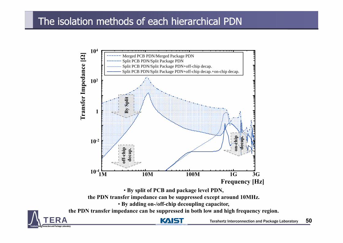
The isolation methods of each hierarchical PDNThe isolation methods of each hierarchical PDN
e [Ω
] 104
Split PCB PDN/Split Package PDNMerged PCB PDN/Merged Package PDN
Split PCB PDN/Split Package PDN+off chip decap
Impe
danc
102
Split PCB PDN/Split Package PDN+off-chip decap.Split PCB PDN/Split Package PDN+off-chip decap.+on-chip decap.
Tran
sfer
I
1 By
Split
10-2
p . on-c
hip
deca
p.
1M 10M 100M 1G 3G10-4
off-
chip
deca
p o d
Frequency [Hz]• By split of PCB and package level PDN,
the PDN transfer impedance can be suppressed except around 10MHz.• By adding on-/off-chip decoupling capacitor
Terahertz Interconnection and Package LaboratoryTERATerahertz Interconnection and Package Laboratory
50
• By adding on-/off-chip decoupling capacitor, the PDN transfer impedance can be suppressed in both low and high frequency region.
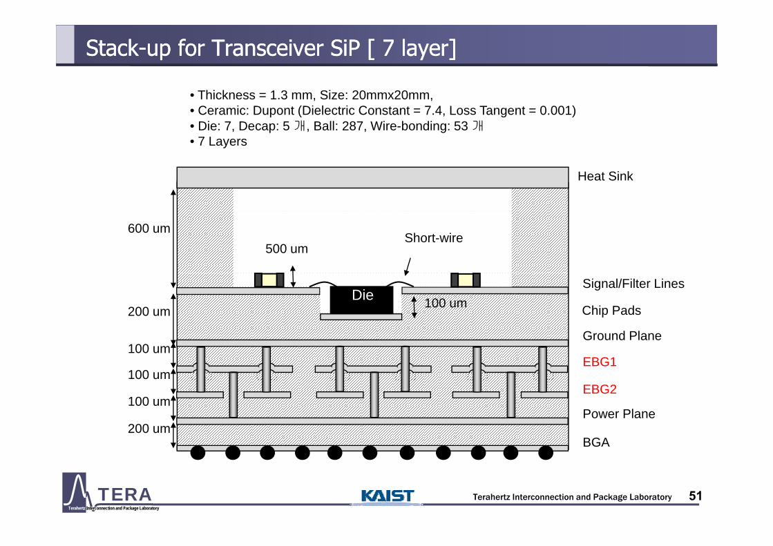
Stack-up for Transceiver SiP [ 7 layer]Stack-up for Transceiver SiP [ 7 layer]
• Thickness = 1.3 mm, Size: 20mmx20mm,• Ceramic: Dupont (Dielectric Constant = 7.4, Loss Tangent = 0.001)• Die: 7, Decap: 5 개, Ball: 287, Wire-bonding: 53 개• 7 Layers
Heat Sink
600 um500 um
Short-wire
Signal/Filter Lines
Ground Plane
Chip PadsDie
200 um 100 um
EBG1
EBG2
Ground Plane
100
100 um
100 um
Power Plane
BGA200 um
100 um
Terahertz Interconnection and Package LaboratoryTERATerahertz Interconnection and Package Laboratory
51

Transceiver without DS-EBGTransceiver without DS-EBG
12 17 dB 12 33 dB-12.17 dBmat 9 GHz
-12.33 dBmat 9GHz
-43 dBm8 999997 GHat 8.999997 GHz
< Without Power/Ground Noise > < With Power/Ground Noise >
Po er/Gro nd noise generates a 43 dBm of n antedPower/Ground noise generates a -43 dBm of unwanted
signal near the output signal.
Terahertz Interconnection and Package LaboratoryTERATerahertz Interconnection and Package Laboratory
52

Transceiver with DS-EBGTransceiver with DS-EBG
12 17 dB 12 33 dB-12.17 dBmat 9 GHz
-12.33 dBmat 9GHz
-64 dBmat 8.999997 GHz
21 dB Suppression
< Without Power/Ground Noise > < With Power/Ground Noise >
DS EBG s ccessf ll s ppresses the n anted signal b 21DS-EBG successfully suppresses the unwanted signal by 21
dB.
Terahertz Interconnection and Package LaboratoryTERATerahertz Interconnection and Package Laboratory
53

Proposed On-Interposer EBG StructureProposed On-Interposer EBG Structure
Capacitive P/G mesh
Width: 80um
Space: 120umW Space: 120umWS
Inductive P/G meshInductive P/G mesh
Width: 40um
Space: 360um
W
SS
Terahertz Interconnection and Package LaboratoryTERATerahertz Interconnection and Package Laboratory
54
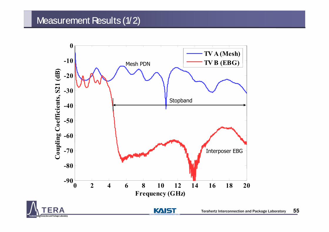
Measurement Results (1/2)Measurement Results (1/2)
-10
0TV A (Mesh)TV B (EBG)Mesh PDN
30
-20
21 (d
B)TV B (EBG)Mesh PDN
-40
-30
ficie
nts,
S
Stopband
-60
-50
ing
Coe
ff
-80
-70
Cou
pl
Interposer EBG
0 2 4 6 8 10 12 14 16 18 20-90
Frequency (GHz)
Terahertz Interconnection and Package LaboratoryTERATerahertz Interconnection and Package Laboratory
55
Frequency (GHz)

Measurement Results (2/2)Measurement Results (2/2)
- Switching noise input at port 1 using 500mVpp clock signal
C l d i t b d t t 2
-10TV A (M h)
-10TV A (M h)
- Coupled noise spectrum probed at port 2
-30
-20
um (d
Bm)
TV A (Mesh)TV B (EBG)
-30
-20
um (d
Bm)
TV A (Mesh)TV B (EBG)
500MHz 1GHz
-50
-40
ed N
oise
Spe
ctru
-50
-40
ed N
oise
Spe
ctru
0 2 4 6 8 10 12 14 16 18 20-70
-60Cou
ple
0 2 4 6 8 10 12 14 16 18 20-70
-60Cou
ple
0 2 4 6 8 10 12 14 16 18 20Frequency (GHz)
0 2 4 6 8 10 12 14 16 18 20Frequency (GHz)
Terahertz Interconnection and Package LaboratoryTERATerahertz Interconnection and Package Laboratory
56

Proposed 3D Clock Distribution SchemeProposed 3D Clock Distribution Scheme
3-D Stacked Chip Star-wiring I/O Clock Distribution for Low Jitter, Skew, and Delay
lossless of bonding-wire & padfree from on both on chip and package power supply noise
Clock Distribution Path using Bonding Wire DLL Output Driver
DLL Replica Path
Star-wiring
DLL
DLL Chip
Stacked Chip
I/O Buffer DLL Chip
Ball Grid Array Package
I/O Buffer
Terahertz Interconnection and Package LaboratoryTERATerahertz Interconnection and Package Laboratory
57

Enhanced Clock Jitter Performance of the Proposed SchemeEnhanced Clock Jitter Performance of the Proposed Scheme
Conventional On-chip I/O Clock Distribution Scheme
3D Stacked Chip Star-wiring I/O Clock Distribution Scheme
300m
V/d
iv]
300m
V/d
iv] 500MHz Clock500MHz Clock
Volta
ge [3
Volta
ge [3
• Peak-to-Peak Jitter : 146ps • Peak-to-Peak Jitter : 34pspRMS Jitter : 22ps
Time[100ps/div]
• Peak-to-Peak Jitter : 34ps RMS Jitter : 5ps
Time[100ps/div]
3D-stacked chip star-wiring clock scheme provides low clock jitter compared with on-chip clock scheme (77% jitter reduction)
It is devised to enable the clock signal delivery to be free from on-chip digital
Terahertz Interconnection and Package LaboratoryTERATerahertz Interconnection and Package Laboratory
58
It is devised to enable the clock signal delivery to be free from on chip digital switching noise and package power/ground cavity noise coupling.

Advantages of Proposed PCR CDN for 3D Stacked Chip PackageAdvantages of Proposed PCR CDN for 3D Stacked Chip Package
Clock path
HRMF/F
Wire-bond as an inductiveterminationDLL
Clock
Data I/O
Synchronous digital chip Quarter-wavelength resonatorJitter is
filteredData I/O
Package sub.
LTCC interposerfiltered
Package ballPackage-level implementation One planar cavity resonator (not grid connected)p y ( g )
• Jitter is filtered by high-Q bandpass filter utilizing a package level quarter-wavelength planar cavity resonator
• Reduction of the number of cascaded repeaters
Terahertz Interconnection and Package LaboratoryTERATerahertz Interconnection and Package Laboratory
5959
• Reduction of the number of cascaded repeaters

Originalities of Proposed PCR CDN for 3D Stacked Chip PackageOriginalities of Proposed PCR CDN for 3D Stacked Chip Package
Wire-bond Standing wave
voltage amplitudesPlanar cavityas an inductivetermination
(V)
voltage amplitudesPlanar cavity
I/Obuffer
I/Obuffer Min.
Max.
• Uniform phase and uniform amplitude standing wave is used for clock distribution
Terahertz Interconnection and Package LaboratoryTERATerahertz Interconnection and Package Laboratory
6060

Quarter-wavelength Resonator with Inductive TerminationQuarter-wavelength Resonator with Inductive Termination
open open open Inductivetermination
Voltage Voltage
Incidentwave
λ/2 λ/4
l
open short
VoltageVoltage
λ/4
Terahertz Interconnection and Package LaboratoryTERATerahertz Interconnection and Package Laboratory
6161

Measure Eyd-diagram of PCR CDN with NoiseMeasure Eyd-diagram of PCR CDN with Noise
1 2
Clock source before distribution Distrbuted clock at planar cavity resonator output
1 2
(V)
1.2
Pk-to-pk jitter= 98 ps Pk-to-pk jitter
= 28 ps
(V)
1.2
Volta
ge
0 Eye-opening= 920mV
Eye-opening= 1720mV
Volta
ge
0
0-1.2
100 200 400300Time (psec)
0 100 200 400300Time (psec)
-1.2
(p ) (p )
Source clock Distrbuted clock• Clock frequnecy : 1.55 GHz
Pk-to-pk jitter 98 ps 28 ps
Eye-opening 920 mV 1720 mV
• Clock magnitude : 1 Vp-p• Switching noise : 300 mV
Terahertz Interconnection and Package LaboratoryTERATerahertz Interconnection and Package Laboratory
6262

Unique Research FocusUnique Research Focus
High-performance Mixed Mode System
System on Chip(On Chip Level) Signal Integrity(On-Chip Level)
System in Package
Signal Integrity
Low Noise and High-Integration y g
(On-Package Level) Co-Design
ElectromagneticI t fP I t it
High-Integration Design
Module, PCB, Cabling(System Level)
InterferencePower Integrity
Improvement of Reliability Performance Design Cycle Cost
Terahertz Interconnection and Package LaboratoryTERATerahertz Interconnection and Package Laboratory
63
Improvement of Reliability, Performance, Design Cycle, Cost

ConclusionConclusion
- Significant noise coupling occurs from digital PDN to noise sensitive RF and analog circuits on a same SiP.
- The clock frequencies and harmonic frequencies should beThe clock frequencies and harmonic frequencies should be placed away from the RF carrier frequencies.
- Low PDN impedance should be maintained.- PDN resonance frequencies should be placed away not only from
the clock frequencies, and their harmonic frequencies, but also from RF carrier frequencies.q
- Via and wire are a major noise coupling path from digital PDN to noise sensitive circuits.Noise coupling reduction methods including using PDN design- Noise coupling reduction methods including using PDN design, frequency control, filtering, separation/isolation, decoupling, shielding, and grounding techniques.
- Case studies: LNA, Clock distribution network- Chip-package co-design can provide optimal and cost-effective
solutions
Terahertz Interconnection and Package LaboratoryTERATerahertz Interconnection and Package Laboratory
64
solutions.