ieee antennas and wireless propagation letters 1...
TRANSCRIPT
1536-1225 (c) 2015 IEEE. Personal use is permitted, but republication/redistribution requires IEEE permission. See http://www.ieee.org/publications_standards/publications/rights/index.html for more information.
This article has been accepted for publication in a future issue of this journal, but has not been fully edited. Content may change prior to final publication. Citation information: DOI 10.1109/LAWP.2016.2539348, IEEEAntennas and Wireless Propagation Letters
IEEE ANTENNAS AND WIRELESS PROPAGATION LETTERS 1
Millimeter-wave IC-Antenna Cointegration forIntegrated Transmitters and Receivers
Yao Liu, Student Member, IEEE, Abhishek Agrawal, Student Member, IEEE, and Arun Natarajan Member, IEEE
Abstract—Advances in CMOS and SiGe technologies havemade mm-wave multi-element arrays with complex architectures,high yields and good inter-element matching feasible. However,Antenna-in-Package approach is challenging with larger numberof array elements due to the increase in mm-wave I/O, the needfor impedance-controlled via/routing symmetry. In this work, wedescribe an antenna-IC co-integration approach that relies onaperture coupling between on-chip feed/ground-plane slot and anantenna-on-substrate to simultaneously achieve wide bandwidthand high efficiency. The proposed approach is validated througha 60-GHz packaged prototype in which a 60-GHz quadruplerand aperture-coupled antenna feed fabricated in a 0.18-µm SiGetechnology is co-integrated with a 60-GHz patch antenna on a100-µm LCP substrate. Measured E-plane and H-plane antennapatterns show 0 dB gain at 61 GHz (corresponding to 40% ef-ficiency) and cross-polarization ratio of ∼10 dB demonstratingthe feasibility of the proposed approach.
Index Terms—On-chip antenna, Aperture-coupled, antenna,co-integration, mm-wave, CMOS, BiCMOS, transceivers, LCP
I. INTRODUCTION
Integrated mm-wave transmit and receive arrays have beendemonstrated in SiGe BiCMOS and CMOS, demonstrating thefeasibility of low-cost multi-functional arrays for communica-tion/imaging applications [1]–[3]. Silicon integration results inexcellent yields and gain/phase matching for complex arrays.This has led to increasing interest in scalable, large-scalearrays with hundreds of elements built using multi-elementunit-cells tiled in X and Y dimensions [1], [2]. While siliconICs can achieve high yields, the mm-wave interface betweenthe IC and the package is challenging for large numberof mm-wave IO. Antenna-in-package (AiP) approaches havebeen investigated for multi-element mm-wave ICs using low-temperature co-fired ceramics (LTCC) and multi-layer organiclaminates (MLO) [4]. However, large number of impedance-controlled lines being routed in a compact area on a packageleads to element-to-element mismatches, need for impedance-controlled vias, and significant routing losses. For example,>1.5-dB interconnect loss in [4] reduces overall efficiency to63% even if 90% antennas efficiency is assumed.
On-chip antennas are attractive for such mm-wave arrays ifcomparable system performance can be achieved. However,silicon substrate has high dielectric constant (∼ 11.7) andoften low resistivity (∼ 10Ω-cm), leading to low efficiencyif EM energy is confined inside the substrate by the antenna.
Yao Liu, Abhishek Agrawal and Arun Natarajan are withthe School of Electrical Engineering and Computer Science,Oregon State University, Corvallis, Oregon, USA 97330 e-mail:(liuyao,agrawala,nataraja)@eecs.oregonstate.edu
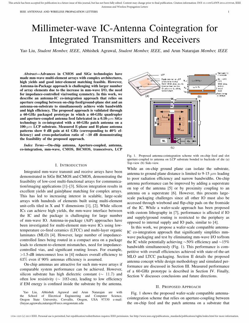
Fig. 1. Proposed antenna-cointegration scheme with on-chip feed and slotaperture-coupled to antenna on LCP substrate bonded to backside of die (a)Top-view (b) Side-view.
While an on-chip ground plane can isolate the substrate,antenna to ground plane distance is limited to 9-15 µm leadingto poor radiation efficiency and narrow bandwidths. On-chipantenna performance can be improved by adding a superstrateon top of the antenna [5] or by proximity coupling to anantenna on a superstrate [6]. However, this presents large-scale packaging challenges since all other IO must also beaccessed through wirebond and flip-chip pads on the frontsideof the IC. While a wafer-scale approach has been proposedwith custom lithography in [7], performance is affected if IOand supply/ground routing is restricted to the periphery asopposed to internal supply and IO pads, similar to [4].
In this work, we propose a wafer-scale compatible antenna-IC co-integration approach that significantly simplifies mm-wave packaging and test by eliminating mm-wave I/O to/fromthe IC while potentially achieving ∼50% efficiency and ∼15%bandwidth simultaneously (Fig. 1). This performance is com-petitive with overall efficiencies achieved with state-of-the-artMLO and LTCC packaging. Section II details the proposedantenna concept while design methodology and simulated per-formance are discussed in Section III. Measured performanceof a 60-GHz prototype is described in Section IV. Finally,Section V discusses conclusions and future directions.
II. PROPOSED APPROACH
Fig. 1 shows the proposed wafer-scale compatible antenna-cointegration scheme that relies on aperture-coupling betweenthe on-chip feed and the patch antenna on a substrate that
1536-1225 (c) 2015 IEEE. Personal use is permitted, but republication/redistribution requires IEEE permission. See http://www.ieee.org/publications_standards/publications/rights/index.html for more information.
This article has been accepted for publication in a future issue of this journal, but has not been fully edited. Content may change prior to final publication. Citation information: DOI 10.1109/LAWP.2016.2539348, IEEEAntennas and Wireless Propagation Letters
IEEE ANTENNAS AND WIRELESS PROPAGATION LETTERS 2
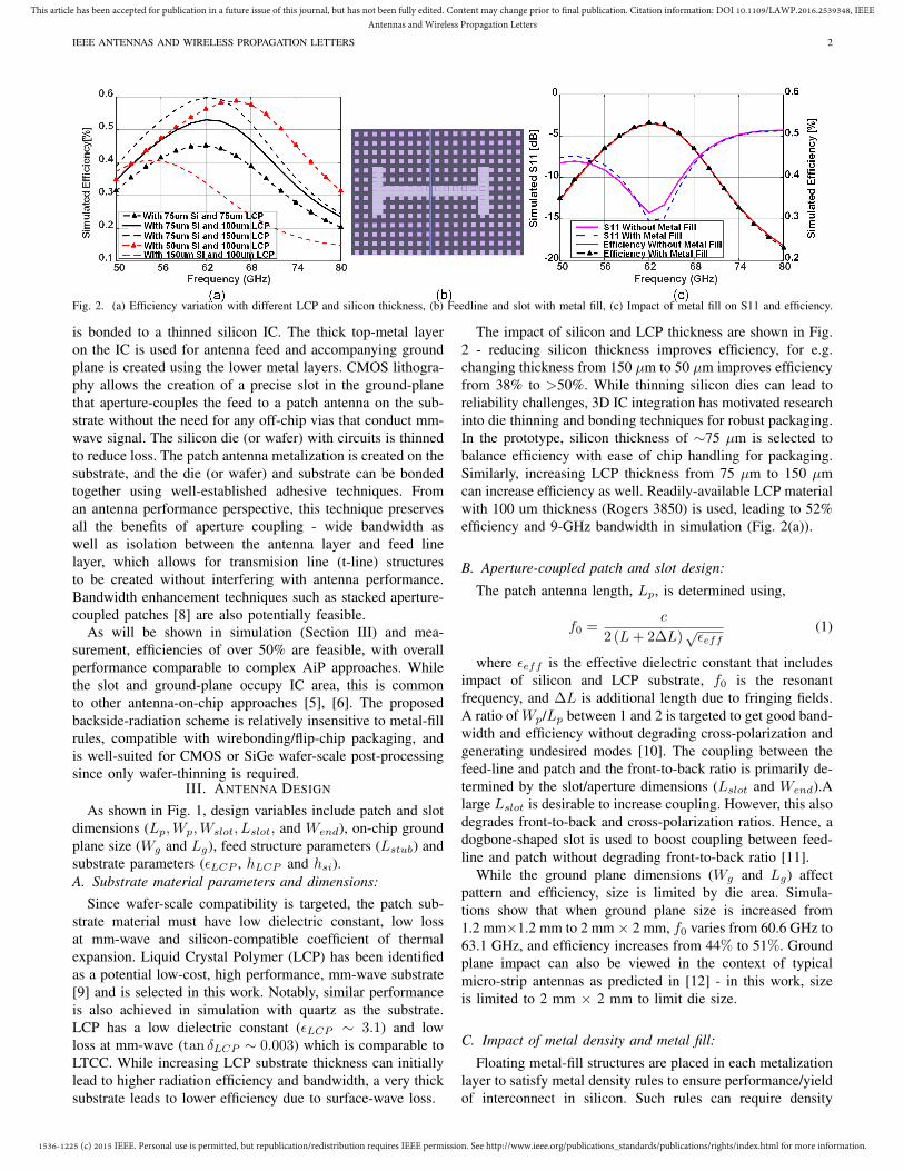
Fig. 2. (a) Efficiency variation with different LCP and silicon thickness, (b) Feedline and slot with metal fill, (c) Impact of metal fill on S11 and efficiency.
is bonded to a thinned silicon IC. The thick top-metal layeron the IC is used for antenna feed and accompanying groundplane is created using the lower metal layers. CMOS lithogra-phy allows the creation of a precise slot in the ground-planethat aperture-couples the feed to a patch antenna on the sub-strate without the need for any off-chip vias that conduct mm-wave signal. The silicon die (or wafer) with circuits is thinnedto reduce loss. The patch antenna metalization is created on thesubstrate, and the die (or wafer) and substrate can be bondedtogether using well-established adhesive techniques. Froman antenna performance perspective, this technique preservesall the benefits of aperture coupling - wide bandwidth aswell as isolation between the antenna layer and feed linelayer, which allows for transmision line (t-line) structuresto be created without interfering with antenna performance.Bandwidth enhancement techniques such as stacked aperture-coupled patches [8] are also potentially feasible.
As will be shown in simulation (Section III) and mea-surement, efficiencies of over 50% are feasible, with overallperformance comparable to complex AiP approaches. Whilethe slot and ground-plane occupy IC area, this is commonto other antenna-on-chip approaches [5], [6]. The proposedbackside-radiation scheme is relatively insensitive to metal-fillrules, compatible with wirebonding/flip-chip packaging, andis well-suited for CMOS or SiGe wafer-scale post-processingsince only wafer-thinning is required.
III. ANTENNA DESIGN
As shown in Fig. 1, design variables include patch and slotdimensions (Lp,Wp,Wslot, Lslot, and Wend), on-chip groundplane size (Wg and Lg), feed structure parameters (Lstub) andsubstrate parameters (εLCP , hLCP and hsi).A. Substrate material parameters and dimensions:
Since wafer-scale compatibility is targeted, the patch sub-strate material must have low dielectric constant, low lossat mm-wave and silicon-compatible coefficient of thermalexpansion. Liquid Crystal Polymer (LCP) has been identifiedas a potential low-cost, high performance, mm-wave substrate[9] and is selected in this work. Notably, similar performanceis also achieved in simulation with quartz as the substrate.LCP has a low dielectric constant (εLCP ∼ 3.1) and lowloss at mm-wave (tan δLCP ∼ 0.003) which is comparable toLTCC. While increasing LCP substrate thickness can initiallylead to higher radiation efficiency and bandwidth, a very thicksubstrate leads to lower efficiency due to surface-wave loss.
The impact of silicon and LCP thickness are shown in Fig.2 - reducing silicon thickness improves efficiency, for e.g.changing thickness from 150 µm to 50 µm improves efficiencyfrom 38% to >50%. While thinning silicon dies can lead toreliability challenges, 3D IC integration has motivated researchinto die thinning and bonding techniques for robust packaging.In the prototype, silicon thickness of ∼75 µm is selected tobalance efficiency with ease of chip handling for packaging.Similarly, increasing LCP thickness from 75 µm to 150 µmcan increase efficiency as well. Readily-available LCP materialwith 100 um thickness (Rogers 3850) is used, leading to 52%efficiency and 9-GHz bandwidth in simulation (Fig. 2(a)).
B. Aperture-coupled patch and slot design:
The patch antenna length, Lp, is determined using,
f0 =c
2 (L+ 2∆L)√εeff
(1)
where εeff is the effective dielectric constant that includesimpact of silicon and LCP substrate, f0 is the resonantfrequency, and ∆L is additional length due to fringing fields.A ratio of Wp/Lp between 1 and 2 is targeted to get good band-width and efficiency without degrading cross-polarization andgenerating undesired modes [10]. The coupling between thefeed-line and patch and the front-to-back ratio is primarily de-termined by the slot/aperture dimensions (Lslot and Wend).Alarge Lslot is desirable to increase coupling. However, this alsodegrades front-to-back and cross-polarization ratios. Hence, adogbone-shaped slot is used to boost coupling between feed-line and patch without degrading front-to-back ratio [11].
While the ground plane dimensions (Wg and Lg) affectpattern and efficiency, size is limited by die area. Simula-tions show that when ground plane size is increased from1.2 mm×1.2 mm to 2 mm× 2 mm, f0 varies from 60.6 GHz to63.1 GHz, and efficiency increases from 44% to 51%. Groundplane impact can also be viewed in the context of typicalmicro-strip antennas as predicted in [12] - in this work, sizeis limited to 2 mm × 2 mm to limit die size.
C. Impact of metal density and metal fill:
Floating metal-fill structures are placed in each metalizationlayer to satisfy metal density rules to ensure performance/yieldof interconnect in silicon. Such rules can require density
1536-1225 (c) 2015 IEEE. Personal use is permitted, but republication/redistribution requires IEEE permission. See http://www.ieee.org/publications_standards/publications/rights/index.html for more information.
This article has been accepted for publication in a future issue of this journal, but has not been fully edited. Content may change prior to final publication. Citation information: DOI 10.1109/LAWP.2016.2539348, IEEEAntennas and Wireless Propagation Letters
IEEE ANTENNAS AND WIRELESS PROPAGATION LETTERS 3
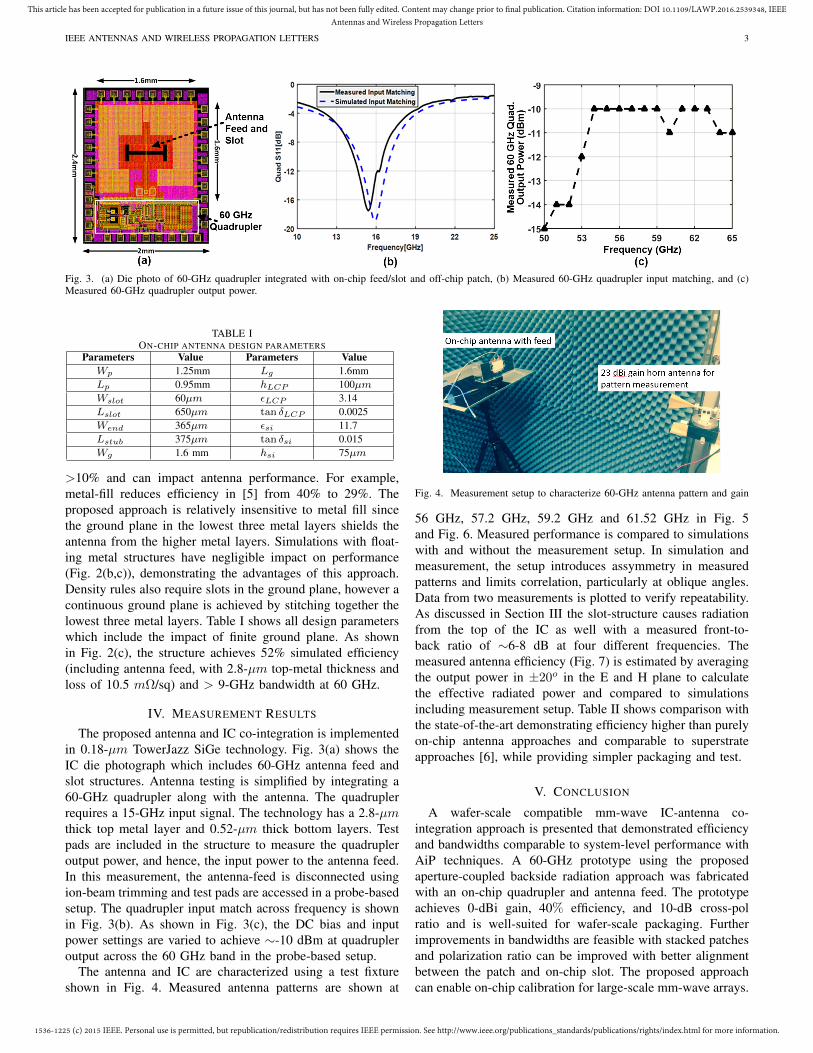
Fig. 3. (a) Die photo of 60-GHz quadrupler integrated with on-chip feed/slot and off-chip patch, (b) Measured 60-GHz quadrupler input matching, and (c)Measured 60-GHz quadrupler output power.
TABLE ION-CHIP ANTENNA DESIGN PARAMETERS
Parameters Value Parameters ValueWp 1.25mm Lg 1.6mmLp 0.95mm hLCP 100µmWslot 60µm εLCP 3.14Lslot 650µm tan δLCP 0.0025Wend 365µm εsi 11.7Lstub 375µm tan δsi 0.015Wg 1.6 mm hsi 75µm
>10% and can impact antenna performance. For example,metal-fill reduces efficiency in [5] from 40% to 29%. Theproposed approach is relatively insensitive to metal fill sincethe ground plane in the lowest three metal layers shields theantenna from the higher metal layers. Simulations with float-ing metal structures have negligible impact on performance(Fig. 2(b,c)), demonstrating the advantages of this approach.Density rules also require slots in the ground plane, however acontinuous ground plane is achieved by stitching together thelowest three metal layers. Table I shows all design parameterswhich include the impact of finite ground plane. As shownin Fig. 2(c), the structure achieves 52% simulated efficiency(including antenna feed, with 2.8-µm top-metal thickness andloss of 10.5 mΩ/sq) and > 9-GHz bandwidth at 60 GHz.
IV. MEASUREMENT RESULTS
The proposed antenna and IC co-integration is implementedin 0.18-µm TowerJazz SiGe technology. Fig. 3(a) shows theIC die photograph which includes 60-GHz antenna feed andslot structures. Antenna testing is simplified by integrating a60-GHz quadrupler along with the antenna. The quadruplerrequires a 15-GHz input signal. The technology has a 2.8-µmthick top metal layer and 0.52-µm thick bottom layers. Testpads are included in the structure to measure the quadrupleroutput power, and hence, the input power to the antenna feed.In this measurement, the antenna-feed is disconnected usingion-beam trimming and test pads are accessed in a probe-basedsetup. The quadrupler input match across frequency is shownin Fig. 3(b). As shown in Fig. 3(c), the DC bias and inputpower settings are varied to achieve ∼-10 dBm at quadrupleroutput across the 60 GHz band in the probe-based setup.
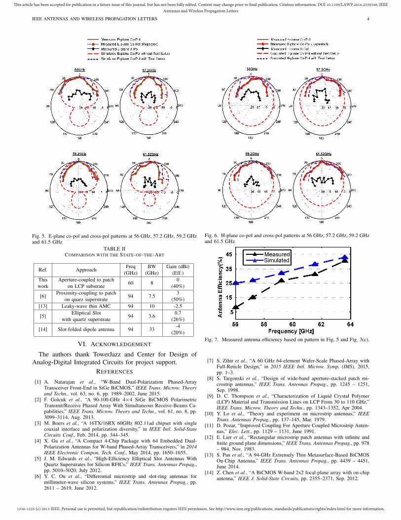
The antenna and IC are characterized using a test fixtureshown in Fig. 4. Measured antenna patterns are shown at
Fig. 4. Measurement setup to characterize 60-GHz antenna pattern and gain
56 GHz, 57.2 GHz, 59.2 GHz and 61.52 GHz in Fig. 5and Fig. 6. Measured performance is compared to simulationswith and without the measurement setup. In simulation andmeasurement, the setup introduces assymmetry in measuredpatterns and limits correlation, particularly at oblique angles.Data from two measurements is plotted to verify repeatability.As discussed in Section III the slot-structure causes radiationfrom the top of the IC as well with a measured front-to-back ratio of ∼6-8 dB at four different frequencies. Themeasured antenna efficiency (Fig. 7) is estimated by averagingthe output power in ±20o in the E and H plane to calculatethe effective radiated power and compared to simulationsincluding measurement setup. Table II shows comparison withthe state-of-the-art demonstrating efficiency higher than purelyon-chip antenna approaches and comparable to superstrateapproaches [6], while providing simpler packaging and test.
V. CONCLUSION
A wafer-scale compatible mm-wave IC-antenna co-integration approach is presented that demonstrated efficiencyand bandwidths comparable to system-level performance withAiP techniques. A 60-GHz prototype using the proposedaperture-coupled backside radiation approach was fabricatedwith an on-chip quadrupler and antenna feed. The prototypeachieves 0-dBi gain, 40% efficiency, and 10-dB cross-polratio and is well-suited for wafer-scale packaging. Furtherimprovements in bandwidths are feasible with stacked patchesand polarization ratio can be improved with better alignmentbetween the patch and on-chip slot. The proposed approachcan enable on-chip calibration for large-scale mm-wave arrays.
1536-1225 (c) 2015 IEEE. Personal use is permitted, but republication/redistribution requires IEEE permission. See http://www.ieee.org/publications_standards/publications/rights/index.html for more information.
This article has been accepted for publication in a future issue of this journal, but has not been fully edited. Content may change prior to final publication. Citation information: DOI 10.1109/LAWP.2016.2539348, IEEEAntennas and Wireless Propagation Letters
IEEE ANTENNAS AND WIRELESS PROPAGATION LETTERS 4
Fig. 5. E-plane co-pol and cross-pol patterns at 56 GHz, 57.2 GHz, 59.2 GHzand 61.5 GHz
TABLE IICOMPARISON WITH THE STATE-OF-THE-ART
Ref. ApproachFreq
(GHz)BW
(GHz)Gain (dBi)
(Eff.)Thiswork
Aperture-coupled to patchon LCP substrate
60 80
(40%)
[6]Proximity-coupling to patch
on quarz superstrate94 7.5
3(50%)
[13] Leaky-wave thin AMC 94 10 -2.5
[5]Elliptical Slot
with quartz superstrate94 3.6
0.7(26%)
[14] Slot-folded dipole antenna 94 33-4
(20%)
VI. ACKNOWLEDGEMENT
The authors thank TowerJazz and Center for Design ofAnalog-Digital Integrated Circuits for project support.
REFERENCES
[1] A. Natarajan et al., “W-Band Dual-Polarization Phased-ArrayTransceiver Front-End in SiGe BiCMOS,” IEEE Trans. Microw. Theoryand Techn., vol. 63, no. 6, pp. 1989–2002, June 2015.
[2] F. Golcuk et al., “A 90-100-GHz 4×4 SiGe BiCMOS PolarimetricTransmit/Receive Phased Array With Simultaneous Receive-Beams Ca-pabilities,” IEEE Trans. Microw. Theory and Techn., vol. 61, no. 8, pp.3099–3114, Aug. 2013.
[3] M. Boers et al., “A 16TX/16RX 60GHz 802.11ad chipset with singlecoaxial interface and polarization diversity,” in IEEE Intl. Solid-StateCircuits Conf., Feb. 2014, pp. 344–345.
[4] X. Gu et al., “A Compact 4-Chip Package with 64 Embedded Dual-Polarization Antennas for W-band Phased-Array Transceivers,” in 2014IEEE Electronic Compon. Tech. Conf., May 2014, pp. 1650–1655.
[5] J. M. Edwards et al., “High-Efficiency Elliptical Slot Antennas WithQuartz Superstrates for Silicon RFICs,” IEEE Trans. Antennas Propag.,pp. 5010–5020, July 2012.
[6] Y. C. Ou et al., “Differential microstrip and slot-ring antennas formillimeter-wave silicon systems,” IEEE Trans. Antennas Propag., pp.2611 – 2619, June 2012.
Fig. 6. H-plane co-pol and cross-pol patterns at 56 GHz, 57.2 GHz, 59.2 GHzand 61.5 GHz
Fig. 7. Measured antenna efficiency based on pattern in Fig. 5 and Fig. 3(c).
[7] S. Zihir et al., “A 60 GHz 64-element Wafer-Scale Phased-Array withFull-Reticle Design,” in 2015 IEEE Intl. Microw. Symp. (IMS), 2015,pp. 1–3.
[8] S. Targonski et al., “Design of wide-band aperture-stacked patch mi-crostrip antennas,” IEEE Trans. Antennas Propag., pp. 1245 – 1251,Sep. 1998.
[9] D. C. Thompson et al., “Characterization of Liquid Crystal Polymer(LCP) Material and Transmission Lines on LCP From 30 to 110 GHz,”IEEE Trans. Microw. Theory and Techn., pp. 1343–1352, Apr 2004.
[10] Y. Lo et al., “Theory and experiment on microstrip antennas,” IEEETrans. Antennas Propag., pp. 137–145, Mar. 1979.
[11] D. Pozar, “Improved Coupling For Aperture Coupled Microstrip Anten-nas,” Elec. Lett., pp. 1129 – 1131, June 1991.
[12] E. Lier et al., “Rectangular microstrip patch antennas with infinite andfinite ground plane dimensions,” IEEE Trans. Antennas Propag., pp. 978– 984, Nov. 1983.
[13] S. Pan et al., “A 94-GHz Extremely Thin Metasurface-Based BiCMOSOn-Chip Antenna,” IEEE Trans. Antennas Propag., pp. 4439 – 4451,June 2014.
[14] Z. Chen et al., “A BiCMOS W-band 2x2 focal-plane array with on-chipantenna,” IEEE J. Solid-State Circuits, pp. 2355–2371, Sep. 2012.