identification cards — integrated circuit cardsidentification cards — integrated circuit cards...
TRANSCRIPT
Reference numberISO/IEC 7816-3:2006(E)
© ISO/IEC 2006
INTERNATIONAL STANDARD
ISO/IEC7816-3
Third edition2006-11-01
Identification cards — Integrated circuit cards — Part 3: Cards with contacts — Electrical interface and transmission protocols
Cartes d'identification — Cartes à circuit intégré —
Partie 3: Cartes à contacts — Interface électrique et protocoles de transmission
ISO/IEC 7816-3:2006(E)
PDF disclaimer This PDF file may contain embedded typefaces. In accordance with Adobe's licensing policy, this file may be printed or viewed but shall not be edited unless the typefaces which are embedded are licensed to and installed on the computer performing the editing. In downloading this file, parties accept therein the responsibility of not infringing Adobe's licensing policy. The ISO Central Secretariat accepts no liability in this area.
Adobe is a trademark of Adobe Systems Incorporated.
Details of the software products used to create this PDF file can be found in the General Info relative to the file; the PDF-creation parameters were optimized for printing. Every care has been taken to ensure that the file is suitable for use by ISO member bodies. In the unlikely event that a problem relating to it is found, please inform the Central Secretariat at the address given below.
© ISO/IEC 2006 All rights reserved. Unless otherwise specified, no part of this publication may be reproduced or utilized in any form or by any means, electronic or mechanical, including photocopying and microfilm, without permission in writing from either ISO at the address below or ISO's member body in the country of the requester.
ISO copyright office Case postale 56 • CH-1211 Geneva 20 Tel. + 41 22 749 01 11 Fax + 41 22 749 09 47 E-mail [email protected] Web www.iso.org
Published in Switzerland
ii © ISO/IEC 2006 – All rights reserved
ISO/IEC 7816-3:2006(E)
© ISO/IEC 2006 – All rights reserved iii
Contents Page
Foreword............................................................................................................................................................ iv Introduction ........................................................................................................................................................ v 1 Scope ..................................................................................................................................................... 1 2 Normative references ........................................................................................................................... 1 3 Terms and definitions........................................................................................................................... 1 4 Symbols and abbreviated terms ......................................................................................................... 3 5 Electrical characteristics ..................................................................................................................... 5 5.1 General................................................................................................................................................... 5 5.2 Contacts................................................................................................................................................. 6 6 Card operating procedure.................................................................................................................... 9 6.1 Principles............................................................................................................................................... 9 6.2 Activation, resets and class selection................................................................................................ 9 6.3 Information exchange......................................................................................................................... 11 6.4 Deactivation......................................................................................................................................... 12 7 Asynchronous character ................................................................................................................... 13 7.1 Elementary time unit........................................................................................................................... 13 7.2 Character frame .................................................................................................................................. 13 7.3 Error signal and character repetition................................................................................................ 14 8 Answer to reset ................................................................................................................................... 15 8.1 Characters and coding conventions................................................................................................. 15 8.2 Answer-to-Reset ................................................................................................................................. 16 8.3 Global interface bytes ........................................................................................................................ 18 9 Protocol and parameters selection................................................................................................... 20 9.1 PPS exchange ..................................................................................................................................... 20 9.2 PPS request and response ................................................................................................................ 20 9.3 Successful PPS exchange ................................................................................................................. 21 10 Protocol T=0, half-duplex transmission of characters ................................................................... 22 10.1 Scope ................................................................................................................................................... 22 10.2 Character level .................................................................................................................................... 22 10.3 Structure and processing of commands.......................................................................................... 22 11 Protocol T=1, half-duplex transmission of blocks .......................................................................... 24 11.1 Scope and principles.......................................................................................................................... 24 11.2 Character frame .................................................................................................................................. 24 11.3 Block frame ......................................................................................................................................... 24 11.4 Protocol parameters ........................................................................................................................... 27 11.5 Character component operation at data link layer.......................................................................... 28 11.6 Block component operation at data link layer................................................................................. 28 12 Transmission of command-response pairs ..................................................................................... 32 12.1 Application protocol data units......................................................................................................... 32 12.2 Command-response pair transmission by T=0 ............................................................................... 34 12.3 Command-response pair transmission by T=1 ............................................................................... 40 Annex A (informative) Scenarios for T=1....................................................................................................... 42 Bibliography ..................................................................................................................................................... 50

ISO/IEC 7816-3:2006(E)
iv © ISO/IEC 2006 – All rights reserved
Foreword
ISO (the International Organization for Standardization) and IEC (the International Electrotechnical Commission) form the specialized system for worldwide standardization. National bodies that are members of ISO or IEC participate in the development of International Standards through technical committees established by the respective organization to deal with particular fields of technical activity. ISO and IEC technical committees collaborate in fields of mutual interest. Other international organizations, governmental and non-governmental, in liaison with ISO and IEC, also take part in the work. In the field of information technology, ISO and IEC have established a joint technical committee, ISO/IEC JTC 1.
International Standards are drafted in accordance with the rules given in the ISO/IEC Directives, Part 2.
The main task of the joint technical committee is to prepare International Standards. Draft International Standards adopted by the joint technical committee are circulated to national bodies for voting. Publication as an International Standard requires approval by at least 75 % of the national bodies casting a vote.
ISO/IEC 7816-3 was prepared by Joint Technical Committee ISO/IEC JTC 1, Information technology, Subcommittee SC 17, Cards and personal identification.
This third edition cancels and replaces the second edition (ISO/IEC 7816-3:1997), which has been technically revised. It also incorporates the Amendment ISO/IEC 7816-3:1997/Amd.1:2002.
In addition, it incorporates material extracted from the first edition of Part 4 (ISO/IEC 7816-4:1995), so that the transmission protocols are no longer present in the second edition of Part 4 (ISO/IEC 7816-4:2005).
ISO/IEC 7816 consists of the following parts, under the general title Identification cards — Integrated circuit cards:
⎯ Part 1: Cards with contacts — Physical characteristics
⎯ Part 2: Cards with contacts — Dimensions and location of the contacts
⎯ Part 3: Cards with contacts — Electrical interface and transmission protocols
⎯ Part 4: Organization, security and commands for interchange
⎯ Part 5: Registration of application providers
⎯ Part 6: Interindustry data elements for interchange
⎯ Part 7: Interindustry commands for Structured Card Query Language (SCQL)
⎯ Part 8: Commands for security operations
⎯ Part 9: Commands for card management
⎯ Part 10: Cards with contacts — Electronic signals and answer to reset for synchronous cards
⎯ Part 11: Personal verification through biometric methods
⎯ Part 12: Cards with contacts — USB electrical interface and operating procedures
⎯ Part 13: Commands for application management in multi-application environment
⎯ Part 15: Cryptographic information application
ISO/IEC 7816-3:2006(E)
© ISO/IEC 2006 – All rights reserved v
Introduction
ISO/IEC 7816 is a series of standards specifying integrated circuit cards and the use of such cards for interchange. These cards are identification cards intended for information exchange negotiated between the outside world and the integrated circuit in the card. As a result of an information exchange, the card delivers information (computation result, stored data), and/or modifies its content (data storage, event memorization).
Five parts are specific to cards with galvanic contacts and three of them specify electrical interfaces.
⎯ ISO/IEC 7816-1 specifies physical characteristics for cards with contacts.
⎯ ISO/IEC 7816-2 specifies dimensions and location of the contacts.
⎯ ISO/IEC 7816-3 specifies electrical interface and transmission protocols for asynchronous cards.
NOTE The first and second editions of ISO/IEC 7816-3 specified an optional use of contact C6 to provide the card with programming power required to write or to erase internal non-volatile memory. As every card manufactured since 1990 internally generates programming power, this third edition deprecates this use, as well as the related indications in the Answer-to-Reset and the related controls in each transmission protocol.
⎯ ISO/IEC 7816-10 specifies electrical interface and answer to reset for synchronous cards.
⎯ ISO/IEC 7816-12 specifies electrical interface and operating procedures for USB cards.
All the other parts are independent of the physical interface technology. They apply to cards accessed by one or more of the following methods: contacts, close coupling and radio frequency.
⎯ ISO/IEC 7816-4 specifies organization, security and commands for interchange.
⎯ ISO/IEC 7816-5 specifies registration of application providers.
⎯ ISO/IEC 7816-6 specifies interindustry data elements for interchange.
⎯ ISO/IEC 7816-7 specifies commands for structured card query language.
⎯ ISO/IEC 7816-8 specifies commands for security operations.
⎯ ISO/IEC 7816-9 specifies commands for card management.
⎯ ISO/IEC 7816-11 specifies personal verification through biometric methods.
⎯ ISO/IEC 7816-13 specifies commands for application management in multi-application environment.
⎯ ISO/IEC 7816-15 specifies cryptographic information application.
ISO/IEC 10536[3] specifies access by close coupling. ISO/IEC 14443[5] and ISO/IEC 15693[6] specify access by radio frequency. Such cards are also known as contactless cards.
ISO/IEC 7816-3:2006(E)
vi © ISO/IEC 2006 – All rights reserved
ISO and IEC draw attention to the fact that it is claimed that compliance with this document may involve the use of patents.
ISO and IEC take no position concerning the evidence, validity and scope of these patent rights.
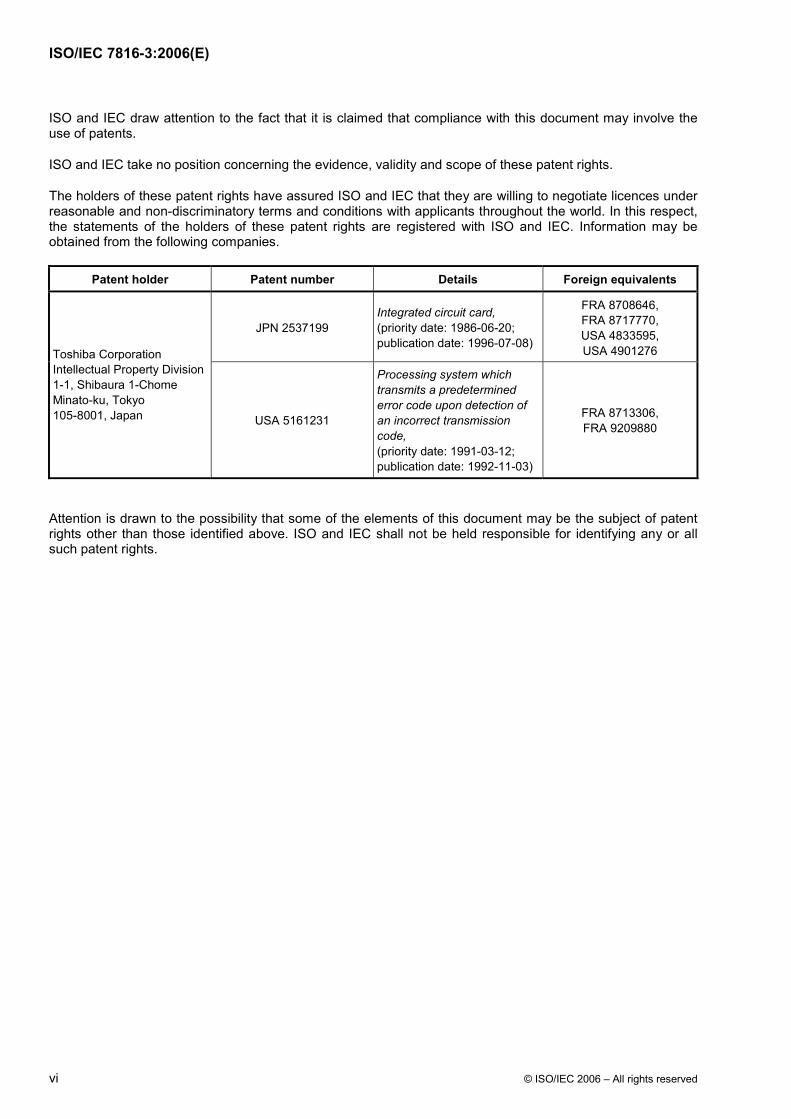
The holders of these patent rights have assured ISO and IEC that they are willing to negotiate licences under reasonable and non-discriminatory terms and conditions with applicants throughout the world. In this respect, the statements of the holders of these patent rights are registered with ISO and IEC. Information may be obtained from the following companies.
Patent holder Patent number Details Foreign equivalents
JPN 2537199 Integrated circuit card, (priority date: 1986-06-20; publication date: 1996-07-08)
FRA 8708646, FRA 8717770, USA 4833595, USA 4901276 Toshiba Corporation
Intellectual Property Division 1-1, Shibaura 1-Chome Minato-ku, Tokyo 105-8001, Japan USA 5161231
Processing system which transmits a predetermined error code upon detection of an incorrect transmission code, (priority date: 1991-03-12; publication date: 1992-11-03)
FRA 8713306, FRA 9209880
Attention is drawn to the possibility that some of the elements of this document may be the subject of patent rights other than those identified above. ISO and IEC shall not be held responsible for identifying any or all such patent rights.
INTERNATIONAL STANDARD ISO/IEC 7816-3:2006(E)
© ISO/IEC 2006 – All rights reserved 1
Identification cards — Integrated circuit cards —
Part 3: Cards with contacts — Electrical interface and transmission protocols
1 Scope
This part of ISO/IEC 7816 specifies the power and signal structures, and information exchange between an integrated circuit card and an interface device such as a terminal.
It also covers signal rates, voltage levels, current values, parity convention, operating procedure, transmission mechanisms and communication with the card.
It does not cover information and instruction content, such as identification of issuers and users, services and limits, security features, journaling and instruction definitions.
2 Normative references
The following referenced documents are indispensable for the application of this document. For dated references, only the edition cited applies. For undated references, the latest edition of the referenced document (including any amendments) applies.
ISO/IEC 7816-2, Identification cards — Integrated circuit cards — Part 2: Cards with contacts — Dimensions and location of the contacts
ISO/IEC 7816-4, Identification cards — Integrated circuit cards — Part 4: Organization, security and commands for interchange
3 Terms and definitions
For the purposes of this document, the following terms and definitions apply.
3.1 block byte string comprising two or three fields defined as prologue field, information field and epilogue field
3.2 class of operating conditions set of values for voltage and current
3.3 cold reset first reset occurring after activation
3.4 destination node address portion of the node address byte, identifying the intended receiver of the block
--`,``,``,,,`,```,`,`,,`,,`,,``-`-`,,`,,`,`,,`---
ISO/IEC 7816-3:2006(E)
2 © ISO/IEC 2006 – All rights reserved
3.5 elementary time unit nominal duration of a moment within an asynchronous character
3.6 epilogue field final field of a block, conveying the error detection code
3.7 identification card card identifying its holder and issuer, which may carry data required as input for the intended use of the card and for transactions based thereon
[ISO/IEC 7810[2]]
3.8 information block block whose primary purpose is to convey application layer information
3.9 information field field of a block, conveying data, generally application data
3.10 interface device terminal, communication device or machine to which the card is electrically connected during operation
3.11 length byte portion of the prologue field, encoding the number of bytes in the information field of the block
3.12 node address byte portion of the prologue field, indicating both destination and source addresses of the block
3.13 operating card card that can correctly carry out all its functions
3.14 procedure byte byte transmitted by the card for indicating the progression of a T=0 command and controlling the exchange of data bytes
3.15 prologue field first field of a block, consisting of three bytes defined as node address, protocol control and length
3.16 protocol control byte portion of the prologue field, encoding transmission control information
3.17 receive ready block block conveying the send-sequence number of the expected I-block, used as a positive or negative acknowledgment
3.18 redundancy code content of the epilogue field, computed from all the bytes in the prologue field and in the information field
ISO/IEC 7816-3:2006(E)
© ISO/IEC 2006 – All rights reserved 3
3.19 source node address portion of the node address byte, identifying the transmitter of the block
3.20 supervisory block block conveying transmission control information
3.21 transmission control function used to control the data transmission between the interface device and the card, including block transmission with sequence control, synchronization and recovery of transmission errors
3.22 warm reset any reset that is not a cold reset
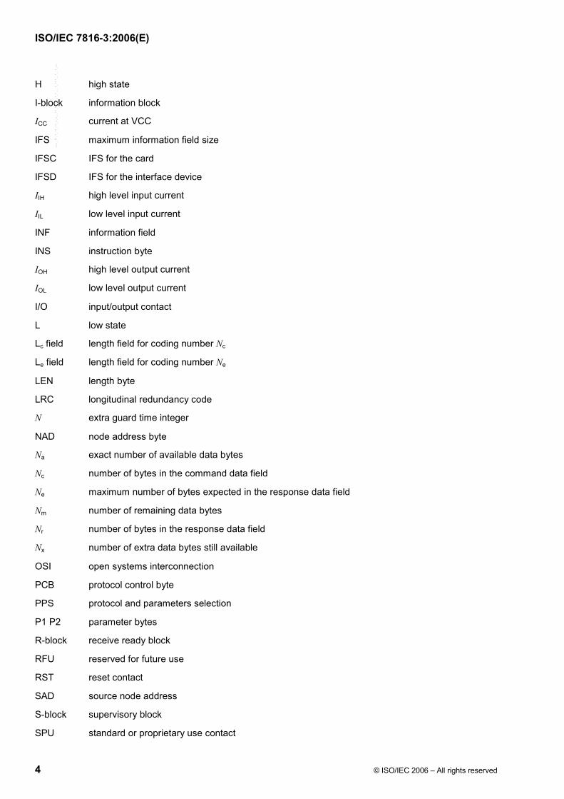
4 Symbols and abbreviated terms
For the purposes of this document, the following symbols and abbreviated terms apply.
A, B, C classes of operating conditions
APDU application protocol data unit
BGT block guard time
BWI block waiting time integer
BWT block waiting time
CGT character guard time
CIN input capacitance
CLA class byte
CLK clock contact
COUT output capacitance
CRC cyclic redundancy code
CWI character waiting time integer
CWT character waiting time
(C(6) C(7)) value of the concatenation of bytes C(6) and C(7) (the first byte is the most significant byte)
D baud rate adjustment integer
DAD destination node address
Dd, Di, Dn default values, indicated values and negotiated values of D
etu elementary time unit
F clock rate conversion integer
f frequency value of the clock signal provided to the card by the interface device
Fd, Fi, Fn default values, indicated values and negotiated values of F
GND ground contact
GT guard time
--`,``,``,,,`,```,`,`,,`,,`,,``-`-`,,`,,`,`,,`---
ISO/IEC 7816-3:2006(E)
4 © ISO/IEC 2006 – All rights reserved
H high state
I-block information block
ICC current at VCC
IFS maximum information field size
IFSC IFS for the card
IFSD IFS for the interface device
IIH high level input current
IIL low level input current
INF information field
INS instruction byte
IOH high level output current
IOL low level output current
I/O input/output contact
L low state
Lc field length field for coding number Nc
Le field length field for coding number Ne
LEN length byte
LRC longitudinal redundancy code
N extra guard time integer
NAD node address byte
Na exact number of available data bytes
Nc number of bytes in the command data field
Ne maximum number of bytes expected in the response data field
Nm number of remaining data bytes
Nr number of bytes in the response data field
Nx number of extra data bytes still available
OSI open systems interconnection
PCB protocol control byte
PPS protocol and parameters selection
P1 P2 parameter bytes
R-block receive ready block
RFU reserved for future use
RST reset contact
SAD source node address
S-block supervisory block
SPU standard or proprietary use contact
--`,``,``,,,`,```,`,`,,`,,`,,``-`-`,,`,,`,`,,`---
ISO/IEC 7816-3:2006(E)
© ISO/IEC 2006 – All rights reserved 5
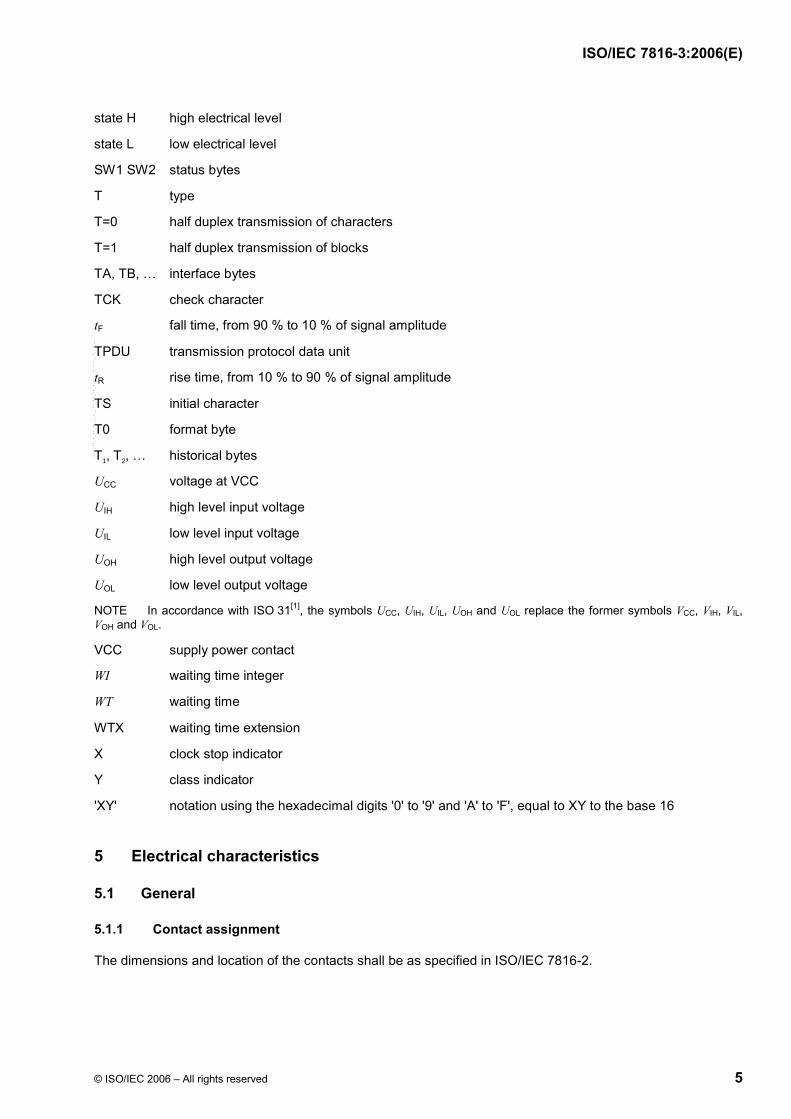
state H high electrical level
state L low electrical level
SW1 SW2 status bytes
T type
T=0 half duplex transmission of characters
T=1 half duplex transmission of blocks
TA, TB, … interface bytes
TCK check character
tF fall time, from 90 % to 10 % of signal amplitude
TPDU transmission protocol data unit
tR rise time, from 10 % to 90 % of signal amplitude
TS initial character
T0 format byte
T1, T2, … historical bytes
UCC voltage at VCC
UIH high level input voltage
UIL low level input voltage
UOH high level output voltage
UOL low level output voltage
NOTE In accordance with ISO 31[1], the symbols UCC, UIH, UIL, UOH and UOL replace the former symbols VCC, VIH, VIL, VOH and VOL.
VCC supply power contact
WI waiting time integer
WT waiting time
WTX waiting time extension
X clock stop indicator
Y class indicator
'XY' notation using the hexadecimal digits '0' to '9' and 'A' to 'F', equal to XY to the base 16
5 Electrical characteristics
5.1 General
5.1.1 Contact assignment
The dimensions and location of the contacts shall be as specified in ISO/IEC 7816-2.
--`,``,``,,,`,```,`,`,,`,,`,,``-`-`,,`,,`,`,,`---
ISO/IEC 7816-3:2006(E)
6 © ISO/IEC 2006 – All rights reserved
This part of ISO/IEC 7816 supports at least the following contacts.
⎯ C1: supply power input (VCC, see 5.2.1).
⎯ C2: reset signal input (RST, see 5.2.2).
⎯ C3: clock signal input (CLK, see 5.2.3).
⎯ C5: ground (GND, reference voltage).
⎯ C6: standard or proprietary use (SPU, see 5.2.4).
⎯ C7: input/output for serial data (I/O, see 5.2.5).
NOTE This document deprecates the use of contact C6 to provide the card with programming power because every card manufactured since 1990 internally generates programming power.
5.1.2 Measurement conventions
By definition, when a card and an interface device are mechanically connected, each contact of the card and the corresponding contact of the interface device together form an “electrical circuit”.
All measurements on an electrical circuit are defined with respect to GND and in an ambient temperature range 0° C to 50° C. All currents flowing into the card are considered positive. All timings shall be measured with respect to the appropriate threshold levels.
By definition, an electrical circuit is “not active” when the voltage with respect to GND remains between 0 V and 0,4 V for currents less than 1 mA flowing into the interface device.
5.1.3 Classes of operating conditions
This document defines three classes of operating conditions, based on the nominal supply voltage provided to the card by the interface device through VCC.
⎯ 5 V for class A.
⎯ 3 V for class B.
⎯ 1,8 V for class C.
The card shall support one or more classes. If the interface device applies a class supported by the card, then the card shall operate as specified.
⎯ If the card supports more than one class, those classes shall be consecutive.
⎯ If the interface device offers more than one class, the order in which those classes are applied is not within the scope of this document.
No card shall be damaged when the interface device applies a class not supported by the card (by definition, a damaged card no longer operates as specified or contains corrupt data).
5.2 Contacts
5.2.1 VCC (C1)
This contact is used to supply the card with power.
ISO/IEC 7816-3:2006(E)
© ISO/IEC 2006 – All rights reserved 7
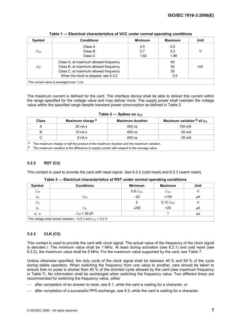
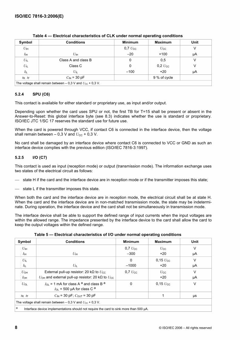
Table 1 — Electrical characteristics of VCC under normal operating conditions Symbol Conditions Minimum Maximum Unit
UCC
Class A Class B Class C
4,5 2,7
1,62
5,5 3,3
1,98
V
ICC
Class A, at maximum allowed frequency Class B, at maximum allowed frequency Class C, at maximum allowed frequency
When the clock is stopped, see 6.3.2
60 50 30
0,5
mA
The current value is averaged over 1 ms.
The maximum current is defined for the card. The interface device shall be able to deliver this current within the range specified for the voltage value and may deliver more. The supply power shall maintain the voltage value within the specified range despite transient power consumption as defined in Table 2.
Table 2 — Spikes on ICC Class Maximum charge a Maximum duration Maximum variation b of ICC
A 20 nA.s 400 ns 100 mA B 10 nA.s 400 ns 50 mA C 6 nA.s 400 ns 30 mA
a The maximum charge is half the product of the maximum duration and the maximum variation. b The maximum variation is the difference in supply current with respect to the average value.
5.2.2 RST (C2)
This contact is used to provide the card with reset signal. See 6.2.2 (cold reset) and 6.2.3 (warm reset).
Table 3 — Electrical characteristics of RST under normal operating conditions Symbol Conditions Minimum Maximum Unit
UIH 0,8 UCC UCC V IIH UIH –20 +150 µA UIL 0 0,12 UCC V IIL UIL –200 +20 µA
tR tF CIN = 30 pF 1 µs The voltage shall remain between – 0,3 V and UCC + 0,3 V.
5.2.3 CLK (C3)
This contact is used to provide the card with clock signal. The actual value of the frequency of the clock signal is denoted f. The minimum value shall be 1 MHz. At least during activation (see 6.2.1) and cold reset (see 6.2.2), the maximum value shall be 5 MHz. For the maximum value supported by the card, see Table 7.
Unless otherwise specified, the duty cycle of the clock signal shall be between 40 % and 60 % of the cycle during stable operation. When switching the frequency from one value to another, care should be taken to ensure that no pulse is shorter than 40 % of the shortest cycle allowed by the card (see maximum frequency in Table 7). No information shall be exchanged when switching the frequency value. Two different times are recommended for switching the frequency value, either ⎯ after completion of an answer to reset, see 8.1, while the card is waiting for a character, or ⎯ after completion of a successful PPS exchange, see 9.3, while the card is waiting for a character.
ISO/IEC 7816-3:2006(E)
8 © ISO/IEC 2006 – All rights reserved
Table 4 — Electrical characteristics of CLK under normal operating conditions Symbol Conditions Minimum Maximum Unit
UIH 0,7 UCC UCC V IIH UIH –20 +100 µA UIL Class A and class B 0 0,5 V UIL Class C 0 0,2 UCC V IIL UIL –100 +20 µA
tR tF CIN = 30 pF 9 % of cycle The voltage shall remain between – 0,3 V and UCC + 0,3 V.
5.2.4 SPU (C6)
This contact is available for either standard or proprietary use, as input and/or output.
Depending upon whether the card uses SPU or not, the first TB for T=15 shall be present or absent in the Answer-to-Reset: this global interface byte (see 8.3) indicates whether the use is standard or proprietary. ISO/IEC JTC 1/SC 17 reserves the standard use for future use.
When the card is powered through VCC, if contact C6 is connected in the interface device, then the voltage shall remain between – 0,3 V and UCC + 0,3 V.
No card shall be damaged by an interface device where contact C6 is connected to VCC or GND as such an interface device complies with the previous edition (ISO/IEC 7816-3:1997).
5.2.5 I/O (C7)
This contact is used as input (reception mode) or output (transmission mode). The information exchange uses two states of the electrical circuit as follows:
⎯ state H if the card and the interface device are in reception mode or if the transmitter imposes this state;
⎯ state L if the transmitter imposes this state.
When both the card and the interface device are in reception mode, the electrical circuit shall be at state H. When the card and the interface device are in non-matched transmission mode, the state may be indetermi-nate. During operation, the interface device and the card shall not be simultaneously in transmission mode.
The interface device shall be able to support the defined range of input currents when the input voltages are within the allowed range. The impedance presented by the interface device to the card shall allow the card to keep the output voltages within the defined range.
Table 5 — Electrical characteristics of I/O under normal operating conditions
Symbol Conditions Minimum Maximum Unit
UIH 0,7 UCC UCC V IIH UIH –300 +20 µA
UIL 0 0,15 UCC V IIL UIL –1000 +20 µA
UOH External pull-up resistor: 20 kΩ to UCC 0,7 UCC UCC V IOH UOH and external pull-up resistor: 20 kΩ to UCC +20 µA
UOL IOL = 1 mA for class A a and class B a IOL = 500 µA for class C a
0 0,15 UCC V
tR tF CIN = 30 pF; COUT = 30 pF 1 µs
The voltage shall remain between – 0,3 V and UCC + 0,3 V.
a Interface device implementations should not require the card to sink more than 500 µA.
--`,``,``,,,`,```,`,`,,`,,`,,``-`-`,,`,,`,`,,`---
ISO/IEC 7816-3:2006(E)
© ISO/IEC 2006 – All rights reserved 9
6 Card operating procedure
6.1 Principles
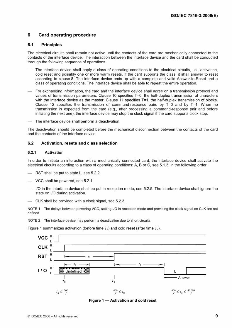
The electrical circuits shall remain not active until the contacts of the card are mechanically connected to the contacts of the interface device. The interaction between the interface device and the card shall be conducted through the following sequence of operations.
⎯ The interface device shall apply a class of operating conditions to the electrical circuits, i.e., activation, cold reset and possibly one or more warm resets. If the card supports the class, it shall answer to reset according to clause 8. The interface device ends up with a complete and valid Answer-to-Reset and a class of operating conditions. The interface device shall be able to repeat the entire operation.
⎯ For exchanging information, the card and the interface device shall agree on a transmission protocol and values of transmission parameters. Clause 10 specifies T=0, the half-duplex transmission of characters with the interface device as the master. Clause 11 specifies T=1, the half-duplex transmission of blocks. Clause 12 specifies the transmission of command-response pairs by T=0 and by T=1. When no transmission is expected from the card (e.g., after processing a command-response pair and before initiating the next one), the interface device may stop the clock signal if the card supports clock stop.
⎯ The interface device shall perform a deactivation.
The deactivation should be completed before the mechanical disconnection between the contacts of the card and the contacts of the interface device.
6.2 Activation, resets and class selection
6.2.1 Activation
In order to initiate an interaction with a mechanically connected card, the interface device shall activate the electrical circuits according to a class of operating conditions: A, B or C, see 5.1.3, in the following order.
⎯ RST shall be put to state L, see 5.2.2.
⎯ VCC shall be powered, see 5.2.1.
⎯ I/O in the interface device shall be put in reception mode, see 5.2.5. The interface device shall ignore the state on I/O during activation.
⎯ CLK shall be provided with a clock signal, see 5.2.3.
NOTE 1 The delays between powering VCC, setting I/O in reception mode and providing the clock signal on CLK are not defined.
NOTE 2 The interface device may perform a deactivation due to short circuits.
Figure 1 summarizes activation (before time Ta) and cold reset (after time Ta).
H L
RST
H L
CLK
H L
VCC
H L I / O Undefined
tb
ta tc
Answer Ta Tb
L
ft 200a ≤ b
400 tf ≤ ff t 000 40c
400 ≤≤
Figure 1 — Activation and cold reset
ISO/IEC 7816-3:2006(E)
10 © ISO/IEC 2006 – All rights reserved
6.2.2 Cold reset
By the end of activation (RST in state L, VCC powered, I/O in reception mode in the interface device, CLK provided with a suitable and stable clock signal), the card is ready for a cold reset. The internal state of the card is not defined before a cold reset.
According to Figure 1, the clock signal is applied to CLK at time Ta. The card shall set I/O to state H within 200 clock cycles (delay ta) after the clock signal is applied to CLK (at time Ta + ta). The cold reset results from maintaining RST at state L for at least 400 clock cycles (delay tb) after the clock signal is applied to CLK (at time Ta + tb). The interface device shall ignore the state on I/O while RST is at state L.
At time Tb, RST is put to state H. The answer on I/O shall begin between 400 and 40 000 clock cycles (delay tc) after the rising edge of the signal on RST (at time Tb + tc). If the answer does not begin within 40 000 clock cycles with RST at state H, the interface device shall perform a deactivation.
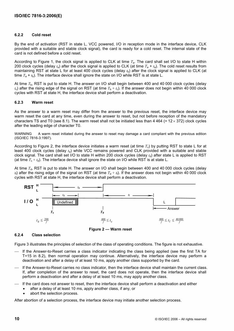
6.2.3 Warm reset
As the answer to a warm reset may differ from the answer to the previous reset, the interface device may warm reset the card at any time, even during the answer to reset, but not before reception of the mandatory characters TS and T0 (see 8.1). The warm reset shall not be initiated less than 4 464 (= 12 × 372) clock cycles after the leading edge of character T0.
WARNING A warm reset initiated during the answer to reset may damage a card compliant with the previous edition (ISO/IEC 7816-3:1997).
According to Figure 2, the interface device initiates a warm reset (at time Tc) by putting RST to state L for at least 400 clock cycles (delay te) while VCC remains powered and CLK provided with a suitable and stable clock signal. The card shall set I/O to state H within 200 clock cycles (delay td) after state L is applied to RST (at time Tc + td). The interface device shall ignore the state on I/O while RST is at state L.
At time Td, RST is put to state H. The answer on I/O shall begin between 400 and 40 000 clock cycles (delay tf) after the rising edge of the signal on RST (at time Td + tf). If the answer does not begin within 40 000 clock cycles with RST at state H, the interface device shall perform a deactivation.
H L
RST
H L
I / O Undefined
te
td tf
Answer Tc Td
L
ft 200d ≤ e
400 tf ≤ ff t 000 40f
400 ≤≤
Figure 2 — Warm reset 6.2.4 Class selection
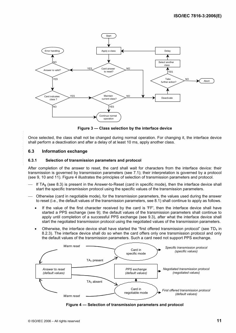
Figure 3 illustrates the principles of selection of the class of operating conditions. The figure is not exhaustive.
⎯ If the Answer-to-Reset carries a class indicator indicating the class being applied (see the first TA for T=15 in 8.2), then normal operation may continue. Alternatively, the interface device may perform a deactivation and after a delay of at least 10 ms, apply another class supported by the card.
⎯ If the Answer-to-Reset carries no class indicator, then the interface device shall maintain the current class. If, after completion of the answer to reset, the card does not operate, then the interface device shall perform a deactivation and after a delay of at least 10 ms, may apply another class.
⎯ If the card does not answer to reset, then the interface device shall perform a deactivation and either • after a delay of at least 10 ms, apply another class, if any, or • abort the selection process.
After abortion of a selection process, the interface device may initiate another selection process.
ISO/IEC 7816-3:2006(E)
© ISO/IEC 2006 – All rights reserved 11
YES
YES
YES
YES
YES
NO
NO
NO
NO
NO
Error handling
Take further action?
Answer is valid?
Card indicates class ?
Card answer to reset?
Maintaincurrent class?
Select another class
Apply a class Delay
Deactivate
Start
Abort
Continue normal operation
Figure 3 — Class selection by the interface device
Once selected, the class shall not be changed during normal operation. For changing it, the interface device shall perform a deactivation and after a delay of at least 10 ms, apply another class.
6.3 Information exchange
6.3.1 Selection of transmission parameters and protocol
After completion of the answer to reset, the card shall wait for characters from the interface device: their transmission is governed by transmission parameters (see 7.1); their interpretation is governed by a protocol (see 9, 10 and 11). Figure 4 illustrates the principles of selection of transmission parameters and protocol.
⎯ If TA2 (see 8.3) is present in the Answer-to-Reset (card in specific mode), then the interface device shall start the specific transmission protocol using the specific values of the transmission parameters.
⎯ Otherwise (card in negotiable mode), for the transmission parameters, the values used during the answer to reset (i.e., the default values of the transmission parameters, see 8.1) shall continue to apply as follows.
• If the value of the first character received by the card is 'FF', then the interface device shall have started a PPS exchange (see 9); the default values of the transmission parameters shall continue to apply until completion of a successful PPS exchange (see 9.3), after what the interface device shall start the negotiated transmission protocol using the negotiated values of the transmission parameters.
• Otherwise, the interface device shall have started the “first offered transmission protocol” (see TD1 in 8.2.3). The interface device shall do so when the card offers only one transmission protocol and only the default values of the transmission parameters. Such a card need not support PPS exchange.
Specific transmission protocol (specific values)
First offered transmission protocol (default values)
Negotiated transmission protocol (negotiated values)
Answer to reset (default values)
Card in negotiable mode
Card in specific mode
Warm reset
Warm reset
TA2 present
TA2 absent
PPS exchange (default values)
Figure 4 — Selection of transmission parameters and protocol
--`,``,``,,,`,```,`,`,,`,,`,,``-`-`,,`,,`,`,,`---
ISO/IEC 7816-3:2006(E)
12 © ISO/IEC 2006 – All rights reserved
NOTE 1 The value of PPSS ('FF', see 9.2) is invalid for CLA (T=0, see 10.3.2) and for NAD (T=1, see 11.3.2.1).
NOTE 2 In a multi-protocol card offering T=0 in negotiable mode, only T=0 can be “implicitly” selected.
NOTE 3 An interface device facing a card in negotiable mode and supporting neither PPS exchange nor the “first offered transmission protocol” can perform either a warm reset or a deactivation.
NOTE 4 A card transmitting character TA2 to an interface device not aware of the existence of specific mode cannot rely on a warm reset to switch the mode.
NOTE 5 An interface device having detected character TA2 should not initiate a warm reset before it detects either an unsupported value in the received characters, or an overrun of WT (see 7.2).
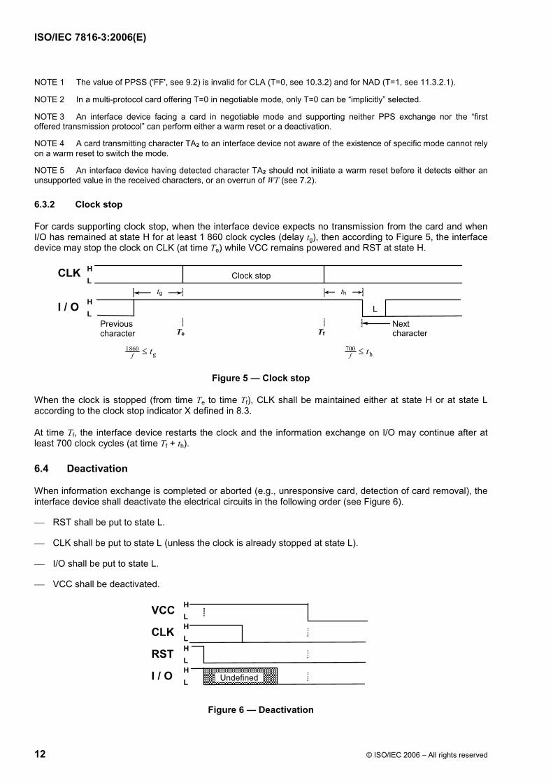
6.3.2 Clock stop
For cards supporting clock stop, when the interface device expects no transmission from the card and when I/O has remained at state H for at least 1 860 clock cycles (delay tg), then according to Figure 5, the interface device may stop the clock on CLK (at time Te) while VCC remains powered and RST at state H.
H L
CLK
H L
I / O tg th
Next character Te Tf
Clock stop
Previous character
L
g860 1 tf ≤ h
700 tf ≤
Figure 5 — Clock stop
When the clock is stopped (from time Te to time Tf), CLK shall be maintained either at state H or at state L according to the clock stop indicator X defined in 8.3.
At time Tf, the interface device restarts the clock and the information exchange on I/O may continue after at least 700 clock cycles (at time Tf + th).
6.4 Deactivation
When information exchange is completed or aborted (e.g., unresponsive card, detection of card removal), the interface device shall deactivate the electrical circuits in the following order (see Figure 6).
⎯ RST shall be put to state L.
⎯ CLK shall be put to state L (unless the clock is already stopped at state L).
⎯ I/O shall be put to state L.
⎯ VCC shall be deactivated.
H L
RST
H L
CLK
H L
VCC
H L
I / O Undefined
Figure 6 — Deactivation
ISO/IEC 7816-3:2006(E)
© ISO/IEC 2006 – All rights reserved 13
7 Asynchronous character
7.1 Elementary time unit
The nominal duration of one moment on the electrical circuit I/O is named “elementary time unit” and denoted etu. The etu shall be equal to F / D clock cycles on the electrical circuit CLK where F and D are the transmission parameters: F is the clock rate conversion integer and D the baud rate adjustment integer.
fDF 1etu 1 ×=
The values of the transmission parameters shall be as specified in 6.3.1.
7.2 Character frame
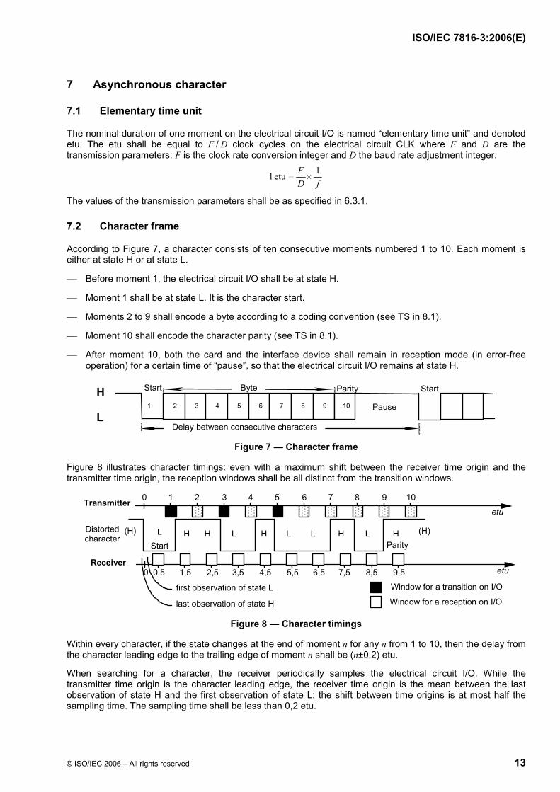
According to Figure 7, a character consists of ten consecutive moments numbered 1 to 10. Each moment is either at state H or at state L.
⎯ Before moment 1, the electrical circuit I/O shall be at state H.
⎯ Moment 1 shall be at state L. It is the character start.
⎯ Moments 2 to 9 shall encode a byte according to a coding convention (see TS in 8.1).
⎯ Moment 10 shall encode the character parity (see TS in 8.1).
⎯ After moment 10, both the card and the interface device shall remain in reception mode (in error-free operation) for a certain time of “pause”, so that the electrical circuit I/O remains at state H.
Parity Start Start H Byte
L 2 103 4 5 6 7 8 91 Pause
Delay between consecutive characters Figure 7 — Character frame
Figure 8 illustrates character timings: even with a maximum shift between the receiver time origin and the transmitter time origin, the reception windows shall be all distinct from the transition windows.
0 1 2 3 4 5 6 7 8 9 10 etu
Start L L L L L H HHH H
0 1,5 2,5 3,5 4,5 5,5 6,5 7,5 8,5 9,5 etu0,5
Transmitter
last observation of state H
first observation of state L Window for a transition on I/O
Window for a reception on I/O
(H)
Receiver
Distorted character
Parity (H)
Figure 8 — Character timings
Within every character, if the state changes at the end of moment n for any n from 1 to 10, then the delay from the character leading edge to the trailing edge of moment n shall be (n±0,2) etu.
When searching for a character, the receiver periodically samples the electrical circuit I/O. While the transmitter time origin is the character leading edge, the receiver time origin is the mean between the last observation of state H and the first observation of state L: the shift between time origins is at most half the sampling time. The sampling time shall be less than 0,2 etu.
ISO/IEC 7816-3:2006(E)
14 © ISO/IEC 2006 – All rights reserved
The receiver shall confirm the start moment before 0,7 etu (in receiver time). The receiver shall read the second moment at (1,5±0,2) etu, the third moment at (2,5±0,2) etu, ... the ninth moment at (8,5±0,2) etu and the parity moment at (9,5±0,2) etu. Character parity is checked on the fly.
The minimum delay between the leading edges of two consecutive characters is named “guard time” and denoted GT.
The maximum delay between the leading edge of a character transmitted by the card and the leading edge of the previous character (transmitted by the card or the interface device) is named “waiting time” and denoted WT. It allows detecting, e.g., an unresponsive card.
NOTE Throughout this document, the guard/waiting times are minimum/maximum delays between the leading edges of consecutive characters.
7.3 Error signal and character repetition
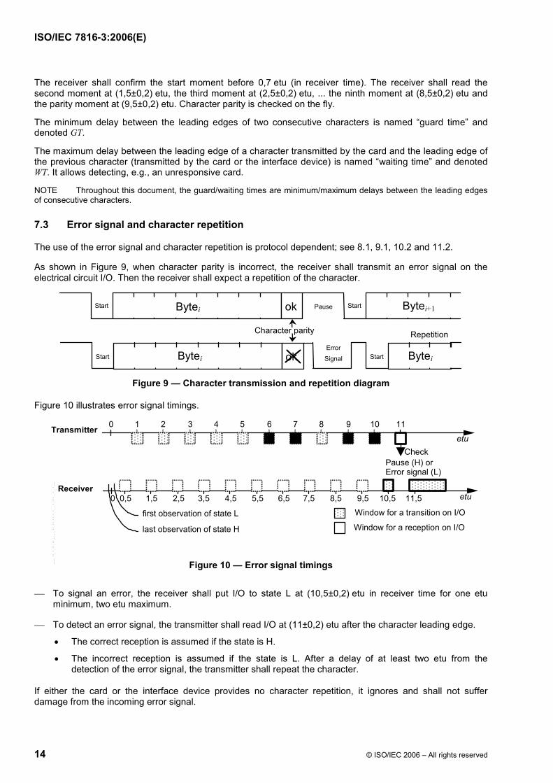
The use of the error signal and character repetition is protocol dependent; see 8.1, 9.1, 10.2 and 11.2.
As shown in Figure 9, when character parity is incorrect, the receiver shall transmit an error signal on the electrical circuit I/O. Then the receiver shall expect a repetition of the character.
Bytei ok
ok
Character parity
Error
Signal
Repetition
Pause Start
StartStart
Start
Bytei Bytei
Bytei+1
Figure 9 — Character transmission and repetition diagram
Figure 10 illustrates error signal timings.
0 1 2 3 4 5 6 7 8 9 10 11 etu
Check
0 1,5 2,5 3,5 4,5 5,5 6,5 7,5 8,5 9,5 10,5 11,5 etu0,5
Transmitter
last observation of state H first observation of state L Window for a transition on I/O
Window for a reception on I/O
Receiver
Pause (H) or Error signal (L)
Figure 10 — Error signal timings
⎯ To signal an error, the receiver shall put I/O to state L at (10,5±0,2) etu in receiver time for one etu minimum, two etu maximum.
⎯ To detect an error signal, the transmitter shall read I/O at (11±0,2) etu after the character leading edge.
• The correct reception is assumed if the state is H.
• The incorrect reception is assumed if the state is L. After a delay of at least two etu from the detection of the error signal, the transmitter shall repeat the character.
If either the card or the interface device provides no character repetition, it ignores and shall not suffer damage from the incoming error signal.
--`,``,``,,,`,```,`,`,,`,,`,,``-`-`,,`,,`,`,,`---
ISO/IEC 7816-3:2006(E)
© ISO/IEC 2006 – All rights reserved 15
8 Answer to reset
8.1 Characters and coding conventions
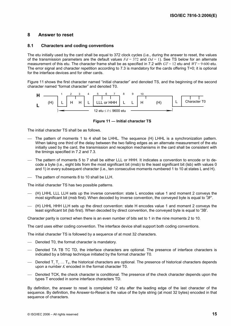
The etu initially used by the card shall be equal to 372 clock cycles (i.e., during the answer to reset, the values of the transmission parameters are the default values Fd = 372 and Dd = 1). See TS below for an alternate measurement of this etu. The character frame shall be as specified in 7.2 with GT = 12 etu and WT = 9 600 etu. The error signal and character repetition according to 7.3 is mandatory for the cards offering T=0; it is optional for the interface devices and for other cards.
Figure 11 shows the first character named “initial character” and denoted TS, and the beginning of the second character named “format character” and denoted T0.
H
L 12 etu ≤ t ≤ 9600 etu
2 3 4 5 6 7 8 9
(H) L H H L LLL or HHH L L H (H)
1 10
L Character T0
Figure 11 — Initial character TS
The initial character TS shall be as follows.
⎯ The pattern of moments 1 to 4 shall be LHHL. The sequence (H) LHHL is a synchronization pattern. When taking one third of the delay between the two falling edges as an alternate measurement of the etu initially used by the card, the transmission and reception mechanisms in the card shall be consistent with the timings specified in 7.2 and 7.3.
⎯ The pattern of moments 5 to 7 shall be either LLL or HHH. It indicates a convention to encode or to de-code a byte (i.e., eight bits from the most significant bit (msb) to the least significant bit (lsb) with values 0 and 1) in every subsequent character (i.e., ten consecutive moments numbered 1 to 10 at states L and H).
⎯ The pattern of moments 8 to 10 shall be LLH.
The initial character TS has two possible patterns.
⎯ (H) LHHL LLL LLH sets up the inverse convention: state L encodes value 1 and moment 2 conveys the most significant bit (msb first). When decoded by inverse convention, the conveyed byte is equal to '3F'.
⎯ (H) LHHL HHH LLH sets up the direct convention: state H encodes value 1 and moment 2 conveys the least significant bit (lsb first). When decoded by direct convention, the conveyed byte is equal to '3B'.
Character parity is correct when there is an even number of bits set to 1 in the nine moments 2 to 10.
The card uses either coding convention. The interface device shall support both coding conventions.
The initial character TS is followed by a sequence of at most 32 characters.
⎯ Denoted T0, the format character is mandatory.
⎯ Denoted TA TB TC TD, the interface characters are optional. The presence of interface characters is indicated by a bitmap technique initiated by the format character T0.
⎯ Denoted T1 T2 … TK, the historical characters are optional. The presence of historical characters depends upon a number K encoded in the format character T0.
⎯ Denoted TCK, the check character is conditional. The presence of the check character depends upon the types T encoded in some interface characters TD.
By definition, the answer to reset is completed 12 etu after the leading edge of the last character of the sequence. By definition, the Answer-to-Reset is the value of the byte string (at most 32 bytes) encoded in that sequence of characters.
ISO/IEC 7816-3:2006(E)
16 © ISO/IEC 2006 – All rights reserved
8.2 Answer-to-Reset
8.2.1 General configuration
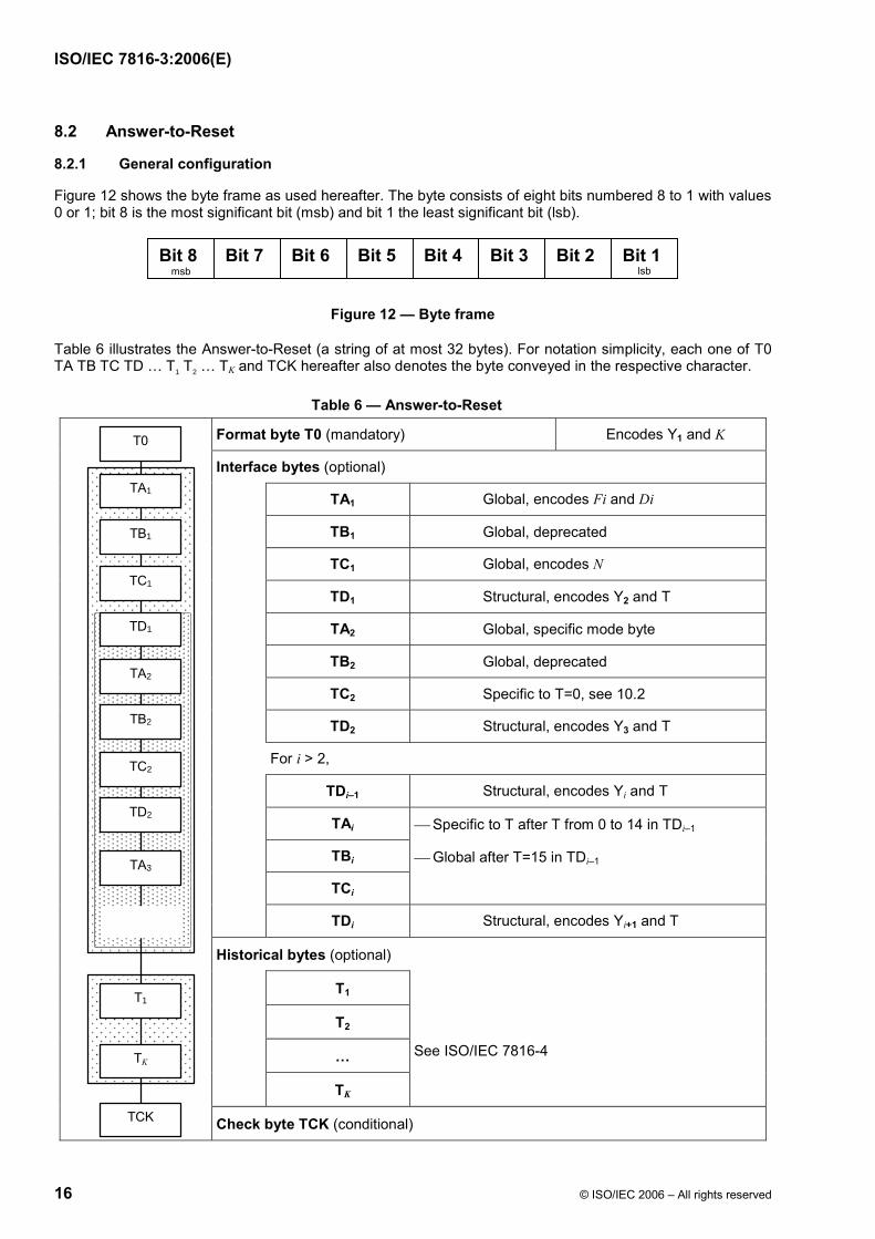
Figure 12 shows the byte frame as used hereafter. The byte consists of eight bits numbered 8 to 1 with values 0 or 1; bit 8 is the most significant bit (msb) and bit 1 the least significant bit (lsb).
Bit 8 msb
Bit 7 Bit 6 Bit 5 Bit 4 Bit 3 Bit 2 Bit 1 lsb
Figure 12 — Byte frame
Table 6 illustrates the Answer-to-Reset (a string of at most 32 bytes). For notation simplicity, each one of T0 TA TB TC TD … T1 T2 … TK and TCK hereafter also denotes the byte conveyed in the respective character.
Table 6 — Answer-to-Reset
Format byte T0 (mandatory) Encodes Y1 and K
Interface bytes (optional)
TA1 Global, encodes Fi and Di
TB1 Global, deprecated
TC1 Global, encodes N
TD1 Structural, encodes Y2 and T
TA2 Global, specific mode byte
TB2 Global, deprecated
TC2 Specific to T=0, see 10.2
TD2 Structural, encodes Y3 and T
For i > 2,
TDi–1 Structural, encodes Yi and T
TAi
TBi
TCi
⎯ Specific to T after T from 0 to 14 in TDi–1
⎯ Global after T=15 in TDi–1
TDi Structural, encodes Yi+1 and T
Historical bytes (optional)
T1
T2
…
TK
See ISO/IEC 7816-4
T0
TA1
TB1
TC1
TD1
TA2
TB2
TC2
TD2
TA3
TCK
T1
TK
Check byte TCK (conditional)
ISO/IEC 7816-3:2006(E)
© ISO/IEC 2006 – All rights reserved 17
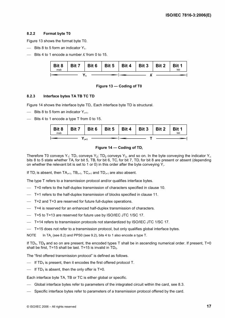
8.2.2 Format byte T0
Figure 13 shows the format byte T0.
⎯ Bits 8 to 5 form an indicator Y1.
⎯ Bits 4 to 1 encode a number K from 0 to 15.
Bit 8 msb
Bit 7 Bit 6 Bit 5 Bit 4 Bit 3 Bit 2 Bit 1 lsb
K Y1
Figure 13 — Coding of T0
8.2.3 Interface bytes TA TB TC TD
Figure 14 shows the interface byte TDi. Each interface byte TD is structural.
⎯ Bits 8 to 5 form an indicator Yi+1.
⎯ Bits 4 to 1 encode a type T from 0 to 15.
Bit 8 msb
Bit 7 Bit 6 Bit 5 Bit 4 Bit 3 Bit 2 Bit 1 lsb
T Yi+1
Figure 14 — Coding of TDi
Therefore T0 conveys Y1; TD1 conveys Y2; TD2 conveys Y3, and so on. In the byte conveying the indicator Yi, bits 8 to 5 state whether TAi for bit 5, TBi for bit 6, TCi for bit 7, TDi for bit 8 are present or absent (depending on whether the relevant bit is set to 1 or 0) in this order after the byte conveying Yi.
If TDi is absent, then TAi+1, TBi+1, TCi+1 and TDi+1 are also absent.
The type T refers to a transmission protocol and/or qualifies interface bytes.
⎯ T=0 refers to the half-duplex transmission of characters specified in clause 10.
⎯ T=1 refers to the half-duplex transmission of blocks specified in clause 11.
⎯ T=2 and T=3 are reserved for future full-duplex operations.
⎯ T=4 is reserved for an enhanced half-duplex transmission of characters.
⎯ T=5 to T=13 are reserved for future use by ISO/IEC JTC 1/SC 17.
⎯ T=14 refers to transmission protocols not standardized by ISO/IEC JTC 1/SC 17.
⎯ T=15 does not refer to a transmission protocol, but only qualifies global interface bytes. NOTE In TA2 (see 8.2) and PPS0 (see 9.2), bits 4 to 1 also encode a type T.
If TD1, TD2 and so on are present, the encoded types T shall be in ascending numerical order. If present, T=0 shall be first, T=15 shall be last. T=15 is invalid in TD1.
The “first offered transmission protocol” is defined as follows.
⎯ If TD1 is present, then it encodes the first offered protocol T.
⎯ If TD1 is absent, then the only offer is T=0.
Each interface byte TA, TB or TC is either global or specific.
⎯ Global interface bytes refer to parameters of the integrated circuit within the card, see 8.3.
⎯ Specific interface bytes refer to parameters of a transmission protocol offered by the card.
ISO/IEC 7816-3:2006(E)
18 © ISO/IEC 2006 – All rights reserved
TA1, TB1, TC1, TA2 and TB2 are global. TC2 is specific to T=0, see 10.2.
The interpretation of TAi TBi TCi for i > 2 depends on the type T encoded in TDi–1.
⎯ After T from 0 to 14, TAi TBi and TCi are specific to the transmission protocol T.
⎯ After T=15, TAi TBi and TCi are global.
If more than three interface bytes TAi TBi TCi TAi+1 TBi+1 TCi+1 … are defined for the same type T, then each one is unambiguously identified by its position after the first, the second … occurrence of T in TDi–1 for i > 2. Consequently, for each type T, the first TA TB TC, the second TA TB TC, and so on, are available.
NOTE The combination of the type T with the bitmap technique allows transmitting only useful interface bytes and when needed, to use default values for parameters corresponding to absent interface bytes.
For example, clause 11.4 specifies three interface bytes specific to T=1, namely the first TA, TB and TC for T=1. If needed, such a byte shall be transmitted respectively as TA3 TB3 and TC3 after TD2 indicating T=1. Depending on whether the card also offers T=0 or not, TD1 shall indicate either T=0 or T=1.
8.2.4 Historical bytes T1 T2 … TK
The historical bytes describe operating characteristics of the card. Their structure and content shall be as specified in ISO/IEC 7816-4.
If K is not zero, then the Answer-to-Reset continues on K (at most 15) historical bytes T1 T2 … TK.
8.2.5 Check byte TCK
If only T=0 is indicated, possibly by default, then TCK shall be absent. If T=0 and T=15 are present and in all the other cases, TCK shall be present. When TCK is present, exclusive-oring all the bytes T0 to TCK inclusive shall give '00'. Any other value is invalid.
8.3 Global interface bytes
This clause specifies the content of the global interface bytes TA1, TB1, TC1, TA2, TB2, the first TA for T=15 and the first TB for T=15.
⎯ If present, such a byte shall be interpreted in order to process correctly any transmission protocol.
⎯ If such a byte is absent, then when needed, default values shall be used for the relevant parameters.
ISO/IEC JTC 1/SC 17 reserves for future use all the global interface bytes not defined in this clause and all the unused values of the global interface bytes defined in this clause.
TA1 encodes the indicated value of the clock rate conversion integer (Fi), the indicated value of the baud rate adjustment integer (Di) and the maximum value of the frequency supported by the card (f (max.)). The default values are Fi = 372, Di = 1 and f (max.) = 5 MHz. For the use of Fi and Di, see 7.1, TC1 and TA2 below, 9.2 and 10.2. For the use of f (max.), see 5.2.3.
⎯ According to Table 7, bits 8 to 5 encode Fi and f (max.).
Table 7 — Fi and f (max.) Bits 8 to 5 0000 0001 0010 0011 0100 0101 0110 0111
Fi 372 372 558 744 1116 1488 1860 RFU
f (max.) MHz 4 5 6 8 12 16 20 —
Bits 8 to 5 1000 1001 1010 1011 1100 1101 1110 1111
Fi RFU 512 768 1024 1536 2048 RFU RFU
f (max.) MHz — 5 7,5 10 15 20 — —
ISO/IEC 7816-3:2006(E)
© ISO/IEC 2006 – All rights reserved 19
⎯ According to Table 8, bits 4 to 1 encode Di.
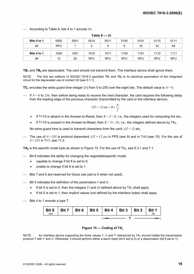
Table 8 — Di Bits 4 to 1 0000 0001 0010 0011 0100 0101 0110 0111
Di RFU 1 2 4 8 16 32 64
Bits 4 to 1 1000 1001 1010 1011 1100 1101 1110 1111
Di 12 20 RFU RFU RFU RFU RFU RFU
TB1 and TB2 are deprecated. The card should not transmit them. The interface device shall ignore them.
NOTE The first two editions of ISO/IEC 7816-3 specified TB1 and TB2 to fix electrical parameters of the integrated circuit for the deprecated use of contact C6 (see 5.1.1).
TC1 encodes the extra guard time integer (N) from 0 to 255 over the eight bits. The default value is N = 0.
⎯ If N = 0 to 254, then before being ready to receive the next character, the card requires the following delay from the leading edge of the previous character (transmitted by the card or the interface device).
GT = fNR ×+etu 12
• If T=15 is absent in the Answer-to-Reset, then R = F / D, i.e., the integers used for computing the etu.
• If T=15 is present in the Answer-to-Reset, then R = Fi / Di, i.e., the integers defined above by TA1.
No extra guard time is used to transmit characters from the card: GT = 12 etu.
⎯ The use of N = 255 is protocol dependent: GT = 12 etu in PPS (see 9) and in T=0 (see 10). For the use of N = 255 in T=1, see 11.2.
TA2 is the specific mode byte as shown in Figure 15. For the use of TA2, see 6.3.1 and 7.1.
⎯ Bit 8 indicates the ability for changing the negotiable/specific mode: • capable to change if bit 8 is set to 0; • unable to change if bit 8 is set to 1.
⎯ Bits 7 and 6 are reserved for future use (set to 0 when not used).
⎯ Bit 5 indicates the definition of the parameters F and D. • If bit 5 is set to 0, then the integers Fi and Di defined above by TA1 shall apply. • If bit 5 is set to 1, then implicit values (not defined by the interface bytes) shall apply.
⎯ Bits 4 to 1 encode a type T.
Bit 8 msb
Bit 7 Bit 6 Bit 5 Bit 4 Bit 3 Bit 2 Bit 1 lsb
T
Figure 15 — Coding of TA2
NOTE An interface device supporting the three values F, D and T referenced by TA2 should initiate the transmission protocol T with F and D. Otherwise, it should perform either a warm reset (bit 8 set to 0) or a deactivation (bit 8 set to 1).
ISO/IEC 7816-3:2006(E)
20 © ISO/IEC 2006 – All rights reserved
The first TA for T=15 encodes the clock stop indicator (X) and the class indicator (Y). The default values are X = “clock stop not supported” and Y = “only class A supported”. For the use of clock stop, see 6.3.2. For the use of the classes of operating conditions, see 6.2.1 and 6.2.4.
⎯ According to Table 9, bits 8 and 7 indicate whether the card supports clock stop (≠ 00) or not (= 00) and, when supported, which state is preferred on the electrical circuit CLK when the clock is stopped.
Table 9 — X
Bits 8 and 7 00 01 10 11 X Clock stop not supported State L State H No preference
⎯ According to Table 10, bits 6 to 1 indicate the classes of operating conditions accepted by the card. Each bit represents a class: bit 1 for class A, bit 2 for class B and bit 3 for class C (see 5.1.3).
Table 10 — Y
Bits 6 to 1 00 0001 00 0010 00 0100 00 0011 00 0110 00 0111 Any other value Y A only B only C only A and B B and C A, B and C RFU
The first TB for T=15 indicates the use of SPU by the card (see 5.2.4). The default value is “SPU not used”.
Coded over bits 7 to 1, the use is either standard (bit 8 set to 0), or proprietary (bit 8 set to 1). The value '00' indicates that the card does not use SPU. ISO/IEC JTC 1/SC 17 reserves for future use any other value where bit 8 is set to 0.
9 Protocol and parameters selection
9.1 PPS exchange
The PPS exchange shall start as specified in 6.3.1. The character frame shall be as specified in 7.1 and 7.2, using the coding convention fixed by TS (see 8.1), with GT as specified in 8.3 and WT = 9 600 etu. The error signal and character repetition according to 7.3 is mandatory for the cards offering T=0; it is optional for the interface devices and for other cards.
Only the interface device is permitted to start the PPS exchange.
⎯ The interface device shall transmit a PPS request to the card.
⎯ If the card receives an erroneous PPS request, it shall not transmit any response.
⎯ If the card receives a correct PPS request, it shall transmit a PPS response, if implemented, or WT will be exceeded.
⎯ In the following three cases: overrun of WT, erroneous PPS response, unsuccessful PPS exchange, the interface device shall perform a deactivation.
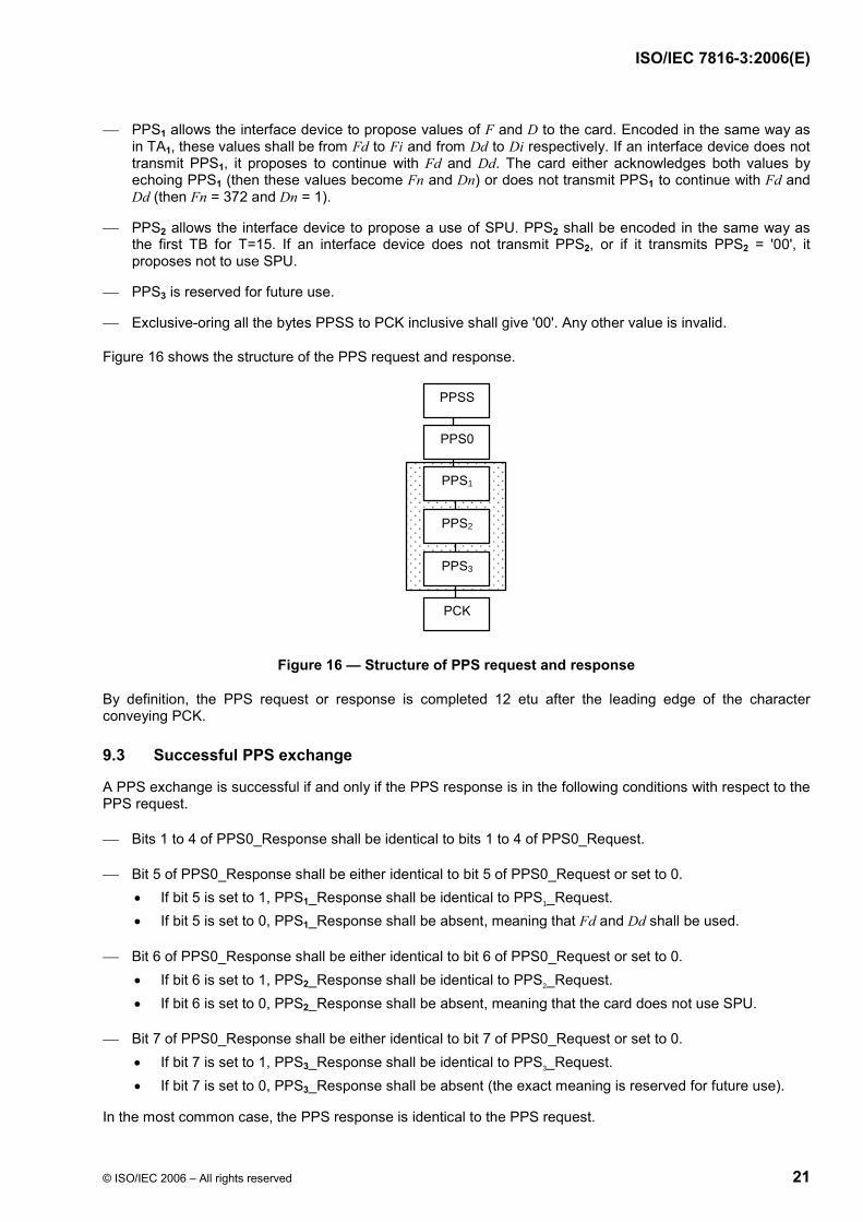
9.2 PPS request and response
The PPS request and PPS response each consist of an initial byte PPSS, followed by a format byte PPS0, three optional parameter bytes PPS1, PPS2, PPS3 and a check byte PCK as the last byte.
⎯ PPSS identifies the PPS request or response and is set to 'FF'.
⎯ In PPS0, each bit 5, 6 or 7 set to 1 indicates the presence of an optional byte PPS1, PPS2, PPS3, respectively. Bits 4 to 1 encode a type T to propose a transmission protocol. Bit 8 is reserved for future use and shall be set to 0.
ISO/IEC 7816-3:2006(E)
© ISO/IEC 2006 – All rights reserved 21
⎯ PPS1 allows the interface device to propose values of F and D to the card. Encoded in the same way as in TA1, these values shall be from Fd to Fi and from Dd to Di respectively. If an interface device does not transmit PPS1, it proposes to continue with Fd and Dd. The card either acknowledges both values by echoing PPS1 (then these values become Fn and Dn) or does not transmit PPS1 to continue with Fd and Dd (then Fn = 372 and Dn = 1).
⎯ PPS2 allows the interface device to propose a use of SPU. PPS2 shall be encoded in the same way as the first TB for T=15. If an interface device does not transmit PPS2, or if it transmits PPS2 = '00', it proposes not to use SPU.
⎯ PPS3 is reserved for future use.
⎯ Exclusive-oring all the bytes PPSS to PCK inclusive shall give '00'. Any other value is invalid.
Figure 16 shows the structure of the PPS request and response.
PPS1
PPS2
PPS3
PPSS
PPS0
PCK
Figure 16 — Structure of PPS request and response
By definition, the PPS request or response is completed 12 etu after the leading edge of the character conveying PCK.
9.3 Successful PPS exchange
A PPS exchange is successful if and only if the PPS response is in the following conditions with respect to the PPS request.
⎯ Bits 1 to 4 of PPS0_Response shall be identical to bits 1 to 4 of PPS0_Request.
⎯ Bit 5 of PPS0_Response shall be either identical to bit 5 of PPS0_Request or set to 0. • If bit 5 is set to 1, PPS1_Response shall be identical to PPS1_Request. • If bit 5 is set to 0, PPS1_Response shall be absent, meaning that Fd and Dd shall be used.
⎯ Bit 6 of PPS0_Response shall be either identical to bit 6 of PPS0_Request or set to 0. • If bit 6 is set to 1, PPS2_Response shall be identical to PPS2_Request. • If bit 6 is set to 0, PPS2_Response shall be absent, meaning that the card does not use SPU.
⎯ Bit 7 of PPS0_Response shall be either identical to bit 7 of PPS0_Request or set to 0. • If bit 7 is set to 1, PPS3_Response shall be identical to PPS3_Request. • If bit 7 is set to 0, PPS3_Response shall be absent (the exact meaning is reserved for future use).
In the most common case, the PPS response is identical to the PPS request.
ISO/IEC 7816-3:2006(E)
22 © ISO/IEC 2006 – All rights reserved
10 Protocol T=0, half-duplex transmission of characters
10.1 Scope
This clause defines the structure and processing of commands in a half-duplex transmission of characters. The interface device initiates these commands. This clause covers transmission control.
10.2 Character level
The transmission protocol shall start as specified in 6.3.1. The character frame shall be as specified in 7.1 and 7.2, using the coding convention fixed by TS (see 8.1), with GT as specified in 8.3. Both the card and the interface device shall use the error signal and character repetition according to 7.3.
When using D = 64, the interface device shall ensure a delay of at least 16 etu between the leading edge of the last received character and the leading edge of the character transmitted for initiating a command.
If present in the Answer-to-Reset, the interface byte TC2 encodes the waiting time integer WI over the eight bits, except the value '00' reserved for future use. If TC2 is absent, then the default value is WI = 10.
The “waiting time” (see 7.2) shall be: f
FiWIWT ××= 960
10.3 Structure and processing of commands
10.3.1 Principles
The interface device initiates every command by transmitting a five-byte header that tells the card what to do. The command processing continues with the transfer of a variable number of data bytes in one direction under the control of procedure bytes transmitted by the card.
It is assumed that the card and the interface device know a priori the direction of transfer, in order to distinguish
⎯ commands for incoming data transfer where the data bytes enter the card while processing, and
⎯ commands for outgoing data transfer where the data bytes leave the card while processing.
10.3.2 Command header
The header consists of five bytes denoted CLA, INS, P1, P2 and P3. The values of CLA, INS, P1 and P2 shall be as specified in ISO/IEC 7816-4.
⎯ CLA denotes a class of commands. The value 'FF' is invalid (reserved for PPSS, see 6.3.1 and 9.2).
NOTE ISO/IEC 7816-4 enforces 'FF' as invalid value of CLA.
⎯ INS denotes an instruction code. The values '6X' and '9X' are invalid.
NOTE ISO/IEC 7816-4 enforces '6X' and '9X' as invalid values of INS.
⎯ P1 P2 denotes an instruction parameter, e.g., a reference completing the instruction code.
⎯ P3 encodes the number of data bytes denoted D1 to Dn to be transferred during the command. • In an outgoing data transfer command, P3='00' introduces a 256-byte data transfer from the card. • In an incoming data transfer command, P3='00' introduces no data transfer.
ISO/IEC 7816-3:2006(E)
© ISO/IEC 2006 – All rights reserved 23
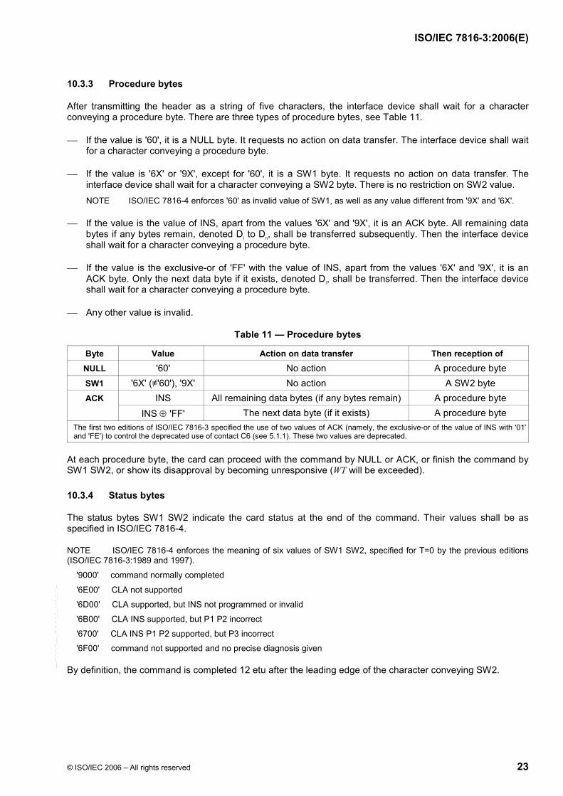
10.3.3 Procedure bytes
After transmitting the header as a string of five characters, the interface device shall wait for a character conveying a procedure byte. There are three types of procedure bytes, see Table 11.
⎯ If the value is '60', it is a NULL byte. It requests no action on data transfer. The interface device shall wait for a character conveying a procedure byte.
⎯ If the value is '6X' or '9X', except for '60', it is a SW1 byte. It requests no action on data transfer. The interface device shall wait for a character conveying a SW2 byte. There is no restriction on SW2 value.
NOTE ISO/IEC 7816-4 enforces '60' as invalid value of SW1, as well as any value different from '9X' and '6X'.
⎯ If the value is the value of INS, apart from the values '6X' and '9X', it is an ACK byte. All remaining data bytes if any bytes remain, denoted Di to Dn, shall be transferred subsequently. Then the interface device shall wait for a character conveying a procedure byte.
⎯ If the value is the exclusive-or of 'FF' with the value of INS, apart from the values '6X' and '9X', it is an ACK byte. Only the next data byte if it exists, denoted Di, shall be transferred. Then the interface device shall wait for a character conveying a procedure byte.
⎯ Any other value is invalid.
Table 11 — Procedure bytes
Byte Value Action on data transfer Then reception of
NULL '60' No action A procedure byte SW1 '6X' (≠'60'), '9X' No action A SW2 byte ACK INS All remaining data bytes (if any bytes remain) A procedure byte
INS ⊕ 'FF' The next data byte (if it exists) A procedure byte The first two editions of ISO/IEC 7816-3 specified the use of two values of ACK (namely, the exclusive-or of the value of INS with '01' and 'FE') to control the deprecated use of contact C6 (see 5.1.1). These two values are deprecated.
At each procedure byte, the card can proceed with the command by NULL or ACK, or finish the command by SW1 SW2, or show its disapproval by becoming unresponsive (WT will be exceeded).
10.3.4 Status bytes
The status bytes SW1 SW2 indicate the card status at the end of the command. Their values shall be as specified in ISO/IEC 7816-4.
NOTE ISO/IEC 7816-4 enforces the meaning of six values of SW1 SW2, specified for T=0 by the previous editions (ISO/IEC 7816-3:1989 and 1997).
'9000' command normally completed
'6E00' CLA not supported
'6D00' CLA supported, but INS not programmed or invalid
'6B00' CLA INS supported, but P1 P2 incorrect
'6700' CLA INS P1 P2 supported, but P3 incorrect
'6F00' command not supported and no precise diagnosis given
By definition, the command is completed 12 etu after the leading edge of the character conveying SW2.
--`,``,``,,,`,```,`,`,,`,,`,,``-`-`,,`,,`,`,,`---
ISO/IEC 7816-3:2006(E)
24 © ISO/IEC 2006 – All rights reserved
11 Protocol T=1, half-duplex transmission of blocks
11.1 Scope and principles
This clause defines the structure and processing of commands in a half-duplex transmission of blocks. A block is a byte string conveyed in asynchronous characters. The interface device and the card may initiate these commands. This clause covers data transmission control such as flow control, block chaining and error correction.
The main characteristics of the transmission protocol are the following.
⎯ The transmission protocol starts with a first block transmitted by the interface device; it continues with alternating the right to transmit a block.
⎯ A block is the smallest data unit that can be exchanged. A block may be used to convey • application data transparent to the transmission protocol, • transmission control data including transmission error handling.
⎯ The block structure allows checking the received block before processing the conveyed data.
The transmission protocol applies the principle of the OSI reference model. Three layers are defined.
⎯ The physical layer transmits moments organized in asynchronous characters according to 11.2.
⎯ The data link layer includes a character component and a block component. • The character component recognizes the beginning and the end of a block according to 11.5. • The block component exchanges blocks according to 11.6.
⎯ The application layer processes commands, which involves the exchange of at least one block or chain of blocks in each direction.
11.2 Character frame
The transmission protocol shall start as specified in 6.3.1. The character frame shall be as specified in 7.1 and 7.2, using the coding convention fixed by TS (see 8.1). The error signal and character repetition according to 7.3 shall not be used. There are two guard times.
⎯ Denoted CGT, the “character guard time” is the minimum delay between the leading edges of two consecutive characters in the same direction of transmission. If N = 0 to 254, CGT = GT as specified in 8.3. If N = 255, CGT = 11 etu in both directions of transmission.
⎯ Denoted BGT, the “block guard time” is the minimum delay between the leading edges of two consecutive characters in opposite directions. BGT = 22 etu.
Character parity allows checking a block in addition to the error detection code (see 11.3.4 and 11.4.4).
11.3 Block frame
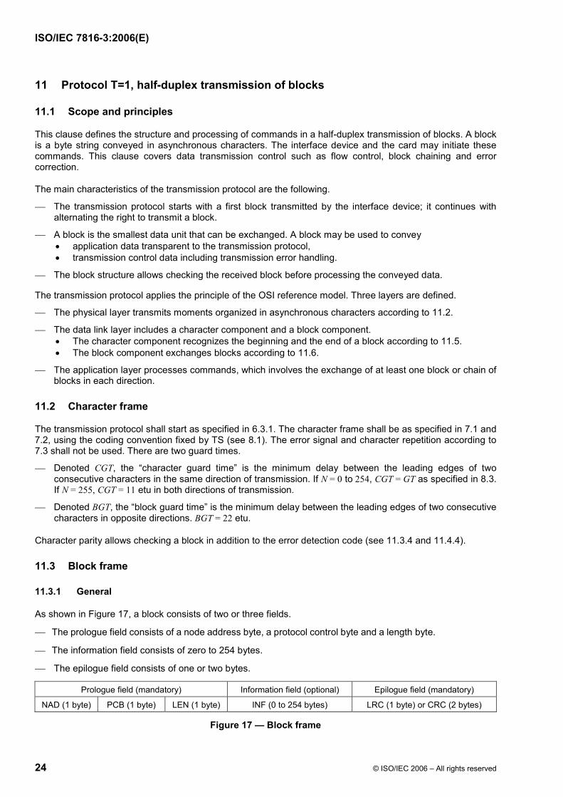
11.3.1 General
As shown in Figure 17, a block consists of two or three fields.
⎯ The prologue field consists of a node address byte, a protocol control byte and a length byte.
⎯ The information field consists of zero to 254 bytes.
⎯ The epilogue field consists of one or two bytes.
Prologue field (mandatory) Information field (optional) Epilogue field (mandatory)
NAD (1 byte) PCB (1 byte) LEN (1 byte) INF (0 to 254 bytes) LRC (1 byte) or CRC (2 bytes)
Figure 17 — Block frame
ISO/IEC 7816-3:2006(E)
© ISO/IEC 2006 – All rights reserved 25
The transmission protocol defines three types of blocks.
⎯ An information block (I-block) is used to convey information for use by the application layer. In addition, it conveys a positive or negative acknowledgment.
⎯ A receive ready block (R-block) is used to convey a positive or negative acknowledgment. Its information field shall be absent.
⎯ A supervisory block (S-block) is used to exchange control information between the interface device and the card. Its information field may be present depending on its controlling function.
NOTE This separation allows the design of the protocol control and the application portions of the device micro code to be relatively independent of each other.
11.3.2 Prologue field
11.3.2.1 Node address byte
The node address byte (NAD) allows identifying the source and the intended destination of the block; it may be used to distinguish between multiple logical connections when they coexist. The value 'FF' is invalid. It is reserved for PPSS (see 6.3.1 and 9.2). Bits 1 to 3 are the source node address denoted SAD and bits 5 to 7 the destination node address denoted DAD. Bits 4 and 8 are deprecated. The card should set them to 00. The interface device shall ignore them.
NOTE The first two editions of ISO/IEC 7816-3 specified bits 4 and 8 to control the deprecated use of contact C6 (see 5.1.1).
When the addressing is not used, the values of SAD and DAD shall be set to 000. Any other value of NAD where SAD and DAD are identical is reserved for future use.
In the first block transmitted by the interface device, NAD shall set up a logical connection by associating the addresses SAD and DAD. Subsequent blocks in which NAD contains the same pair of addresses SAD and DAD are associated with the same logical connection. During information exchange, other pairs of addresses SAD and DAD may set up other logical connections.
NOTE For example, blocks transmitted by the interface device with the values x for SAD and y for DAD and blocks transmitted by the card with the values y for SAD and x for DAD belong to a logical connection denoted (x, y), whereas blocks transmitted by the interface device with the values v for SAD and w for DAD and blocks transmitted by the card with the values w for SAD and v for DAD belong to another logical connection (v, w).
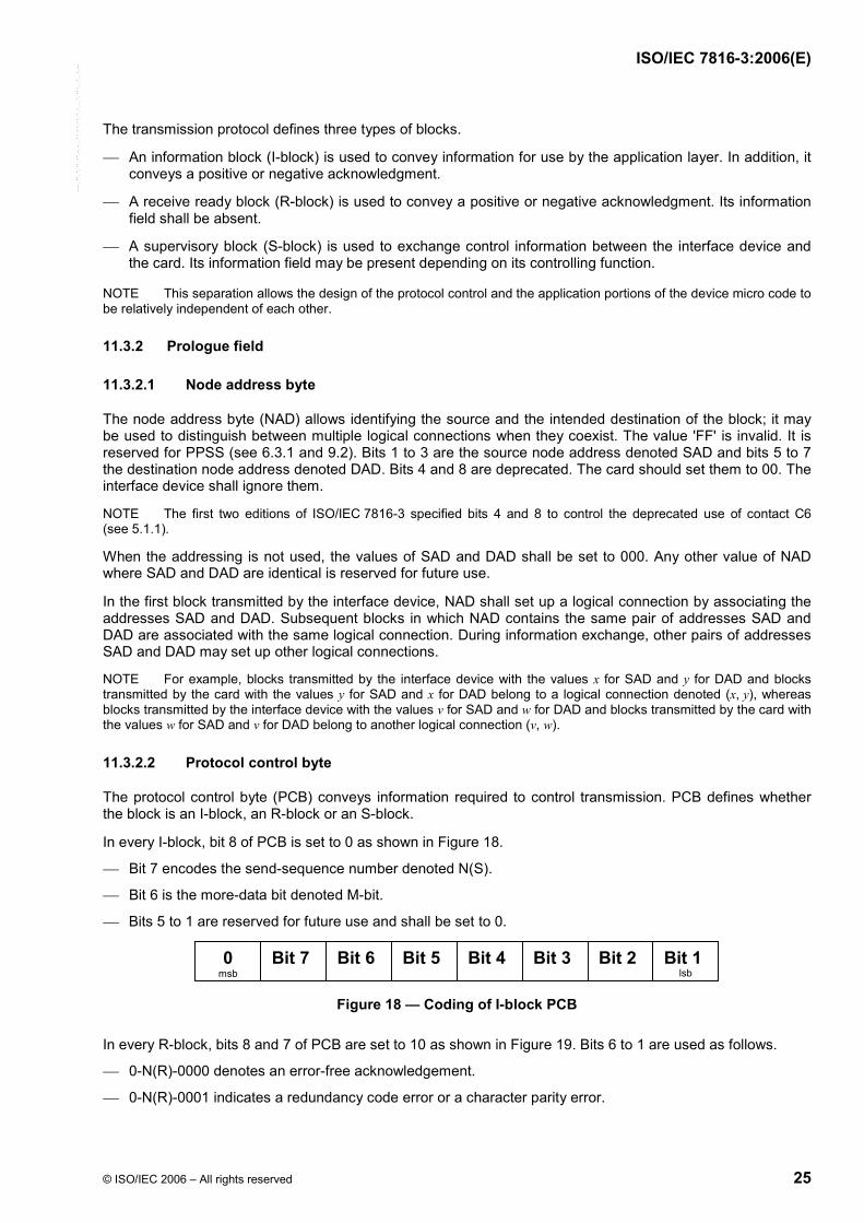
11.3.2.2 Protocol control byte
The protocol control byte (PCB) conveys information required to control transmission. PCB defines whether the block is an I-block, an R-block or an S-block.
In every I-block, bit 8 of PCB is set to 0 as shown in Figure 18.
⎯ Bit 7 encodes the send-sequence number denoted N(S).
⎯ Bit 6 is the more-data bit denoted M-bit.
⎯ Bits 5 to 1 are reserved for future use and shall be set to 0.
0 msb
Bit 7 Bit 6 Bit 5 Bit 4 Bit 3 Bit 2 Bit 1 lsb
Figure 18 — Coding of I-block PCB
In every R-block, bits 8 and 7 of PCB are set to 10 as shown in Figure 19. Bits 6 to 1 are used as follows.
⎯ 0-N(R)-0000 denotes an error-free acknowledgement.
⎯ 0-N(R)-0001 indicates a redundancy code error or a character parity error.
--`,``,``,,,`,```,`,`,,`,,`,,``-`-`,,`,,`,`,,`---
ISO/IEC 7816-3:2006(E)
26 © ISO/IEC 2006 – All rights reserved
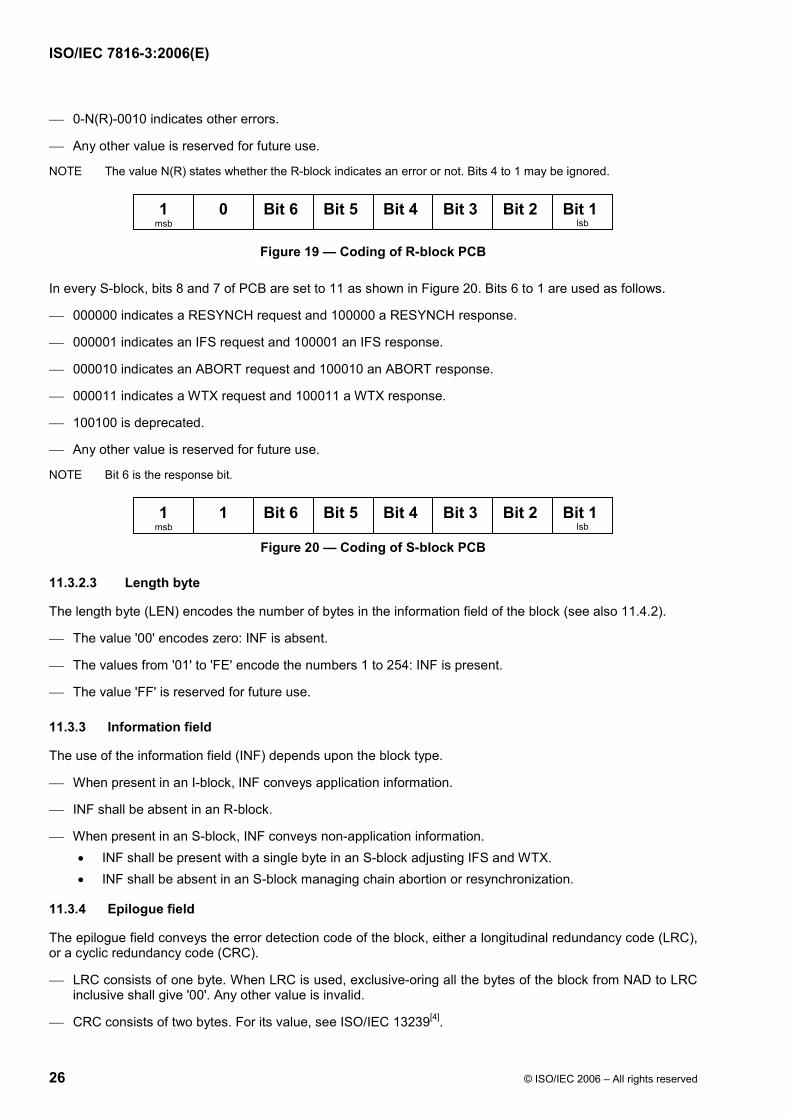
⎯ 0-N(R)-0010 indicates other errors.
⎯ Any other value is reserved for future use.
NOTE The value N(R) states whether the R-block indicates an error or not. Bits 4 to 1 may be ignored.
1 msb
0 Bit 6 Bit 5 Bit 4 Bit 3 Bit 2 Bit 1 lsb
Figure 19 — Coding of R-block PCB
In every S-block, bits 8 and 7 of PCB are set to 11 as shown in Figure 20. Bits 6 to 1 are used as follows.
⎯ 000000 indicates a RESYNCH request and 100000 a RESYNCH response.
⎯ 000001 indicates an IFS request and 100001 an IFS response.
⎯ 000010 indicates an ABORT request and 100010 an ABORT response.
⎯ 000011 indicates a WTX request and 100011 a WTX response.
⎯ 100100 is deprecated.
⎯ Any other value is reserved for future use.
NOTE Bit 6 is the response bit.
1 msb
1 Bit 6 Bit 5 Bit 4 Bit 3 Bit 2 Bit 1 lsb
Figure 20 — Coding of S-block PCB
11.3.2.3 Length byte
The length byte (LEN) encodes the number of bytes in the information field of the block (see also 11.4.2).
⎯ The value '00' encodes zero: INF is absent.
⎯ The values from '01' to 'FE' encode the numbers 1 to 254: INF is present.
⎯ The value 'FF' is reserved for future use.
11.3.3 Information field
The use of the information field (INF) depends upon the block type.
⎯ When present in an I-block, INF conveys application information.
⎯ INF shall be absent in an R-block.
⎯ When present in an S-block, INF conveys non-application information. • INF shall be present with a single byte in an S-block adjusting IFS and WTX. • INF shall be absent in an S-block managing chain abortion or resynchronization.
11.3.4 Epilogue field
The epilogue field conveys the error detection code of the block, either a longitudinal redundancy code (LRC), or a cyclic redundancy code (CRC).
⎯ LRC consists of one byte. When LRC is used, exclusive-oring all the bytes of the block from NAD to LRC inclusive shall give '00'. Any other value is invalid.
⎯ CRC consists of two bytes. For its value, see ISO/IEC 13239[4].
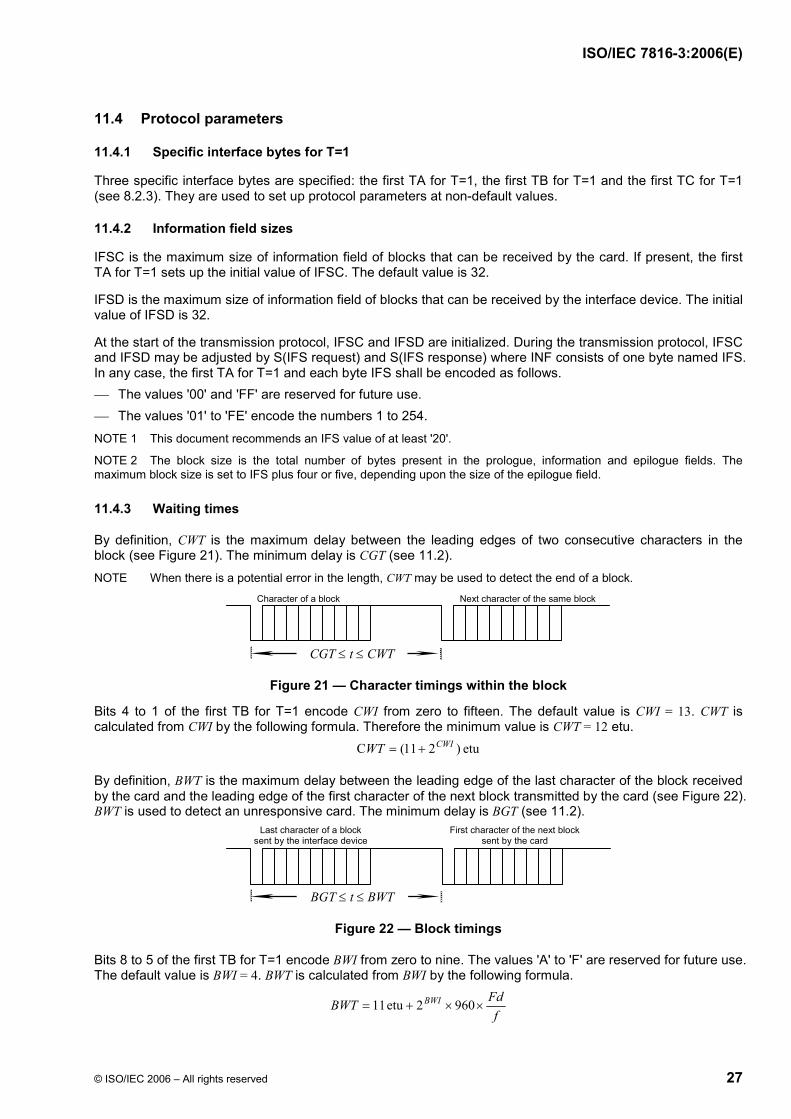
ISO/IEC 7816-3:2006(E)
© ISO/IEC 2006 – All rights reserved 27
11.4 Protocol parameters
11.4.1 Specific interface bytes for T=1
Three specific interface bytes are specified: the first TA for T=1, the first TB for T=1 and the first TC for T=1 (see 8.2.3). They are used to set up protocol parameters at non-default values.
11.4.2 Information field sizes
IFSC is the maximum size of information field of blocks that can be received by the card. If present, the first TA for T=1 sets up the initial value of IFSC. The default value is 32.
IFSD is the maximum size of information field of blocks that can be received by the interface device. The initial value of IFSD is 32.
At the start of the transmission protocol, IFSC and IFSD are initialized. During the transmission protocol, IFSC and IFSD may be adjusted by S(IFS request) and S(IFS response) where INF consists of one byte named IFS. In any case, the first TA for T=1 and each byte IFS shall be encoded as follows. ⎯ The values '00' and 'FF' are reserved for future use. ⎯ The values '01' to 'FE' encode the numbers 1 to 254.
NOTE 1 This document recommends an IFS value of at least '20'.
NOTE 2 The block size is the total number of bytes present in the prologue, information and epilogue fields. The maximum block size is set to IFS plus four or five, depending upon the size of the epilogue field.
11.4.3 Waiting times
By definition, CWT is the maximum delay between the leading edges of two consecutive characters in the block (see Figure 21). The minimum delay is CGT (see 11.2).
NOTE When there is a potential error in the length, CWT may be used to detect the end of a block.
Character of a block Next character of the same block
CGT ≤ t ≤ CWT
Figure 21 — Character timings within the block
Bits 4 to 1 of the first TB for T=1 encode CWI from zero to fifteen. The default value is CWI = 13. CWT is calculated from CWI by the following formula. Therefore the minimum value is CWT = 12 etu.
etu )211(C CWIWT +=
By definition, BWT is the maximum delay between the leading edge of the last character of the block received by the card and the leading edge of the first character of the next block transmitted by the card (see Figure 22). BWT is used to detect an unresponsive card. The minimum delay is BGT (see 11.2).
Last character of a block sent by the interface device
First character of the next block sent by the card
BGT ≤ t ≤ BWT
Figure 22 — Block timings
Bits 8 to 5 of the first TB for T=1 encode BWI from zero to nine. The values 'A' to 'F' are reserved for future use. The default value is BWI = 4. BWT is calculated from BWI by the following formula.
fFdBWT BWI ××+= 9602etu 11
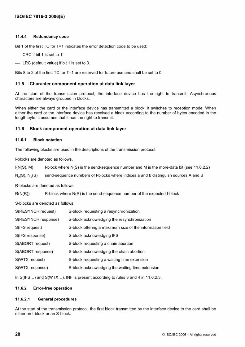
ISO/IEC 7816-3:2006(E)
28 © ISO/IEC 2006 – All rights reserved
11.4.4 Redundancy code
Bit 1 of the first TC for T=1 indicates the error detection code to be used:
⎯ CRC if bit 1 is set to 1;
⎯ LRC (default value) if bit 1 is set to 0.
Bits 8 to 2 of the first TC for T=1 are reserved for future use and shall be set to 0.
11.5 Character component operation at data link layer
At the start of the transmission protocol, the interface device has the right to transmit. Asynchronous characters are always grouped in blocks.
When either the card or the interface device has transmitted a block, it switches to reception mode. When either the card or the interface device has received a block according to the number of bytes encoded in the length byte, it assumes that it has the right to transmit.
11.6 Block component operation at data link layer
11.6.1 Block notation
The following blocks are used in the descriptions of the transmission protocol.
I-blocks are denoted as follows.
I(N(S), M) I-block where N(S) is the send-sequence number and M is the more-data bit (see 11.6.2.2)
Na(S), Nb(S) send-sequence numbers of I-blocks where indices a and b distinguish sources A and B
R-blocks are denoted as follows.
R(N(R)) R-block where N(R) is the send-sequence number of the expected I-block
S-blocks are denoted as follows.
S(RESYNCH request) S-block requesting a resynchronization
S(RESYNCH response) S-block acknowledging the resynchronization
S(IFS request) S-block offering a maximum size of the information field
S(IFS response) S-block acknowledging IFS
S(ABORT request) S-block requesting a chain abortion
S(ABORT response) S-block acknowledging the chain abortion
S(WTX request) S-block requesting a waiting time extension
S(WTX response) S-block acknowledging the waiting time extension
In S(IFS…) and S(WTX…), INF is present according to rules 3 and 4 in 11.6.2.3.
11.6.2 Error-free operation
11.6.2.1 General procedures
At the start of the transmission protocol, the first block transmitted by the interface device to the card shall be either an I-block or an S-block.
--`,``,``,,,`,```,`,`,,`,,`,,``-`-`,,`,,`,`,,`---
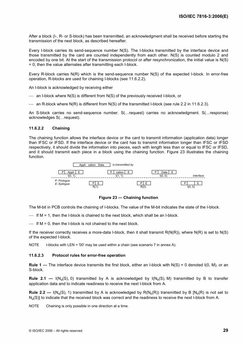
ISO/IEC 7816-3:2006(E)
© ISO/IEC 2006 – All rights reserved 29
After a block (I-, R- or S-block) has been transmitted, an acknowledgment shall be received before starting the transmission of the next block, as described hereafter.
Every I-block carries its send-sequence number N(S). The I-blocks transmitted by the interface device and those transmitted by the card are counted independently from each other. N(S) is counted modulo 2 and encoded by one bit. At the start of the transmission protocol or after resynchronization, the initial value is N(S) = 0; then the value alternates after transmitting each I-block.
Every R-block carries N(R) which is the send-sequence number N(S) of the expected I-block. In error-free operation, R-blocks are used for chaining I-blocks (see 11.6.2.2).
An I-block is acknowledged by receiving either
⎯ an I-block where N(S) is different from N(S) of the previously received I-block, or
⎯ an R-block where N(R) is different from N(S) of the transmitted I-block (see rule 2.2 in 11.6.2.3).
An S-block carries no send-sequence number. S(…request) carries no acknowledgment. S(…response) acknowledges S(…request).
11.6.2.2 Chaining
The chaining function allows the interface device or the card to transmit information (application data) longer than IFSC or IFSD. If the interface device or the card has to transmit information longer than IFSC or IFSD respectively, it should divide the information into pieces, each with length less than or equal to IFSC or IFSD, and it should transmit each piece in a block using the chaining function. Figure 23 illustrates the chaining function.
Appli cation Data is transmitted by
P Appli E P cation E P Data E Interface
P E R(1)
P ER(0)
P E I(0, 0)
I(0, 0)I(1, 1)I(0, 1)
P: Prologue E: Epilogue
Figure 23 — Chaining function
The M-bit in PCB controls the chaining of I-blocks. The value of the M-bit indicates the state of the I-block.
⎯ If M = 1, then the I-block is chained to the next block, which shall be an I-block.
⎯ If M = 0, then the I-block is not chained to the next block.
If the receiver correctly receives a more-data I-block, then it shall transmit R(N(R)), where N(R) is set to N(S) of the expected I-block.
NOTE I-blocks with LEN = '00' may be used within a chain (see scenario 7 in annex A).
11.6.2.3 Protocol rules for error-free operation
Rule 1 — The interface device transmits the first block, either an I-block with N(S) = 0 denoted I(0, M), or an S-block.
Rule 2.1 — I(Na(S), 0) transmitted by A is acknowledged by I(Nb(S), M) transmitted by B to transfer application data and to indicate readiness to receive the next I-block from A.
Rule 2.2 — I(Na(S), 1) transmitted by A is acknowledged by R(Nb(R)) transmitted by B [Nb(R) is not set to Na(S)] to indicate that the received block was correct and the readiness to receive the next I-block from A.
NOTE Chaining is only possible in one direction at a time.
ISO/IEC 7816-3:2006(E)
30 © ISO/IEC 2006 – All rights reserved
Rule 3 — If the card requires more than BWT to process the previously received I-block, it transmits S(WTX request) where INF conveys one byte encoding an integer multiplier of the BWT value. The interface device shall acknowledge by S(WTX response) with the same INF.
The time allocated starts at the leading edge of the last character of S(WTX response).
Rule 4 — The card transmits S(IFS request) to indicate a new IFSC it can support. The interface device shall acknowledge by S(IFS response) with the same INF. The interface device assumes the new IFSC is valid as long as no other IFSC is indicated by another S(IFS request).
The interface device transmits S(IFS request) to indicate a new IFSD it can support. The card shall acknowledge by S(IFS response) with the same INF. The card assumes the new IFSD is valid as long as no other IFSD is indicated by another S(IFS request).
For the encoding of IFSC and IFSD in INF, see 11.4.2.
Rule 5 — Chaining is indicated by the M-bit, where I(N(S), 0) is a non-chained block or the last block of a chain. I(N(S), 1) is a part of a chain and shall be followed by at least one chained block.
R(N(R)) requests transmission of the next chained I-block I(N(S) = N(R), …) and acknowledges the received chained I-block I(NOT N(R), 1).
11.6.3 Error-handling
11.6.3.1 Errors detected by the receiver
The tasks of the block layer are to transmit blocks, to detect transmission and sequence errors, to handle such errors and to resynchronize the transmission protocol. Therefore the block component of the data link layer should be able to handle the following errors.
⎯ BWT time-out — The card did not transmit any character within the specified delay.
⎯ Reception of an invalid block — Examples are
• character parity error(s),
• redundancy code error,
• invalid PCB (due to unknown encoding),
• invalid LEN (transmission error or incompatibility with the block type or with IFSC or IFSD),
• loss of synchronization because the block size and the number encoded by LEN are inconsistent,
• failure to receive the relevant S(… response) after having transmitted S(… request).
Resynchronization of the transmission protocol may be attempted at three consecutive levels. If one level is unsuccessful, then the next level is tried.
⎯ For the interface device, the three levels are
• retransmission of blocks,
• use of S(RESYNCH request),
• warm reset or deactivation.
⎯ For the card, the three levels are
• retransmission of blocks,
• use of S(RESYNCH response),
• without action by the interface device, the card becomes unresponsive.
--`,``,``,,,`,```,`,`,,`,,`,,``-`-`,,`,,`,`,,`---
ISO/IEC 7816-3:2006(E)
© ISO/IEC 2006 – All rights reserved 31
11.6.3.2 Protocol rules for error-handling
Rule 6 — S(RESYNCH request) may be transmitted only by the interface device to reach resynchronization and to initiate resetting the communication parameters of the transmission protocol to its initial values.
Rule 6.1 — If the receiver detects a loss of synchronization, it gets back the right to transmit after a silence on the electrical circuit I/O greater than the larger of CWT or BGT.
Rule 6.2 — S(RESYNCH request) shall be responded to by S(RESYNCH response) from the card.
Rule 6.3 — After the interface device has received S(RESYNCH response), the transmission protocol is initiated.
Rule 6.4 — After the interface device has failed a maximum of three times in succession to reach the intended resynchronization by transmitting S(RESYNCH request), it performs either a warm reset or a deactivation.
Rule 6.5 — When S(RESYNCH request) is received, the previously transmitted block is assumed not to have been received.
Rule 7.1 — When an I-block was transmitted and an invalid block is received or a BWT time-out (with the interface device) occurs, an R-block is transmitted, which requests with its N(R) for the expected I-block with N(S) = N(R).
Rule 7.2 — When an R-block was transmitted and an invalid block is received or a BWT time-out (with the interface device) occurs, this R-block is retransmitted.
Rule 7.3 — When S(… request) was transmitted and the received response is not S(… response) or a BWT time-out occurs (only with the interface device), S(… request) is retransmitted.
When S(… response) was transmitted and an invalid block is received or a BWT time-out occurs (only with the interface device), an R-block is transmitted.
Rule 7.4.1 — After failing to receive an error-free block at the start of the transmission protocol, the interface device makes a maximum of two further attempts in succession before performing either a warm reset or a deactivation.
Rule 7.4.2 — During the transmission protocol, if the interface device fails to receive an error-free block, it makes a maximum of two further attempts in succession before transmitting S(RESYNCH request).
Rule 7.4.3 — If the card fails to receive an error-free block after a second attempt in succession, it remains in reception mode.
Rule 7.5 — On receiving an invalid first block, the card reacts by transmitting R(0).
Rule 7.6 — If the first block transmitted by the interface device is not responded to within BWT, the interface device transmits R(0).
Rule 8 — When the card transmits S(IFS request) and receives an invalid block, it retransmits a maximum of one more S(IFS request) in order to elicit an S(IFS response). After the second failure, it remains in reception mode.
Rule 9 — The abortion of a chain can be initiated by either the transmitter or receiver of a chain transmitting S(ABORT request) which shall be answered by S(ABORT response), after what an R-block may be transmitted depending on whether it is necessary to give back the right to transmit.
NOTE Abortion of chaining may be due to physical errors in the card, such as memory error.
--`,``,``,,,`,```,`,`,,`,,`,,``-`-`,,`,,`,`,,`---
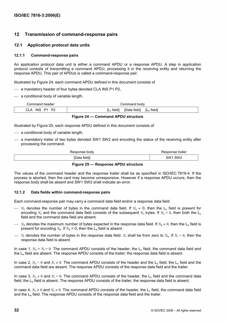
ISO/IEC 7816-3:2006(E)
32 © ISO/IEC 2006 – All rights reserved
12 Transmission of command-response pairs
12.1 Application protocol data units
12.1.1 Command-response pairs
An application protocol data unit is either a command APDU or a response APDU. A step in application protocol consists of transmitting a command APDU, processing it in the receiving entity and returning the response APDU. This pair of APDUs is called a command-response pair.
Illustrated by Figure 24, each command APDU defined in this document consists of
⎯ a mandatory header of four bytes denoted CLA INS P1 P2,
⎯ a conditional body of variable length.
Command header Command body
CLA INS P1 P2 [Lc field] [Data field] [Le field]
Figure 24 — Command APDU structure
Illustrated by Figure 25, each response APDU defined in this document consists of
⎯ a conditional body of variable length,
⎯ a mandatory trailer of two bytes denoted SW1 SW2 and encoding the status of the receiving entity after processing the command.
Response body Response trailer
[Data field] SW1 SW2
Figure 25 — Response APDU structure
The values of the command header and the response trailer shall be as specified in ISO/IEC 7816-4. If the process is aborted, then the card may become unresponsive. However if a response APDU occurs, then the response body shall be absent and SW1 SW2 shall indicate an error.
12.1.2 Data fields within command-response pairs
Each command-response pair may carry a command data field and/or a response data field.
⎯ Nc denotes the number of bytes in the command data field. If Nc ≠ 0, then the Lc field is present for encoding Nc and the command data field consists of the subsequent Nc bytes. If Nc = 0, then both the Lc field and the command data field are absent.
⎯ Ne denotes the maximum number of bytes expected in the response data field. If Ne ≠ 0, then the Le field is present for encoding Ne. If Ne = 0, then the Le field is absent.
⎯ Nr denotes the number of bytes in the response data field. Nr shall be from zero to Ne. If Nr = 0, then the response data field is absent.
In case 1, Nc = Nr = 0. The command APDU consists of the header; the Lc field, the command data field and the Le field are absent. The response APDU consists of the trailer; the response data field is absent.
In case 2, Nc = 0 and Nr ≠ 0. The command APDU consists of the header and the Le field; the Lc field and the command data field are absent. The response APDU consists of the response data field and the trailer.
In case 3, Nc ≠ 0 and Nr = 0. The command APDU consists of the header, the Lc field and the command data field; the Le field is absent. The response APDU consists of the trailer; the response data field is absent.
In case 4, Nc ≠ 0 and Nr ≠ 0. The command APDU consists of the header, the Lc field, the command data field and the Le field. The response APDU consists of the response data field and the trailer.
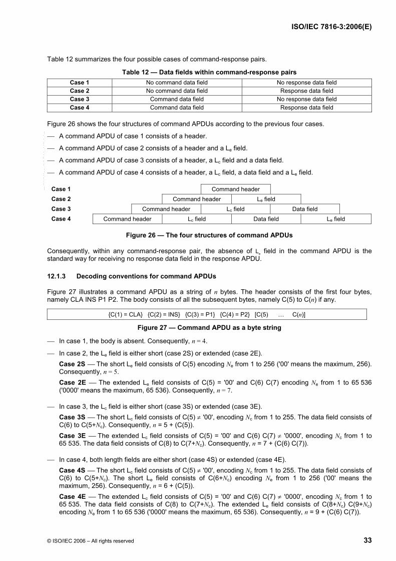
ISO/IEC 7816-3:2006(E)
© ISO/IEC 2006 – All rights reserved 33
Table 12 summarizes the four possible cases of command-response pairs.
Table 12 — Data fields within command-response pairs Case 1 No command data field No response data field Case 2 No command data field Response data field Case 3 Command data field No response data field Case 4 Command data field Response data field
Figure 26 shows the four structures of command APDUs according to the previous four cases.
⎯ A command APDU of case 1 consists of a header.
⎯ A command APDU of case 2 consists of a header and a Le field.
⎯ A command APDU of case 3 consists of a header, a Lc field and a data field.
⎯ A command APDU of case 4 consists of a header, a Lc field, a data field and a Le field.
Case 1 Command header Case 2 Command header Le field Case 3 Command header Lc field Data field Case 4 Command header Lc field Data field Le field
Figure 26 — The four structures of command APDUs
Consequently, within any command-response pair, the absence of Le field in the command APDU is the standard way for receiving no response data field in the response APDU.
12.1.3 Decoding conventions for command APDUs
Figure 27 illustrates a command APDU as a string of n bytes. The header consists of the first four bytes, namely CLA INS P1 P2. The body consists of all the subsequent bytes, namely C(5) to C(n) if any.
C(1) = CLA C(2) = INS C(3) = P1 C(4) = P2 [C(5) … C(n)]
Figure 27 — Command APDU as a byte string
⎯ In case 1, the body is absent. Consequently, n = 4.
⎯ In case 2, the Le field is either short (case 2S) or extended (case 2E). Case 2S ⎯ The short Le field consists of C(5) encoding Ne from 1 to 256 ('00' means the maximum, 256). Consequently, n = 5. Case 2E ⎯ The extended Le field consists of C(5) = '00' and C(6) C(7) encoding Ne from 1 to 65 536 ('0000' means the maximum, 65 536). Consequently, n = 7.
⎯ In case 3, the Lc field is either short (case 3S) or extended (case 3E). Case 3S ⎯ The short Lc field consists of C(5) ≠ '00', encoding Nc from 1 to 255. The data field consists of C(6) to C(5+Nc). Consequently, n = 5 + (C(5)). Case 3E ⎯ The extended Lc field consists of C(5) = '00' and C(6) C(7) ≠ '0000', encoding Nc from 1 to 65 535. The data field consists of C(8) to C(7+Nc). Consequently, n = 7 + (C(6) C(7)).
⎯ In case 4, both length fields are either short (case 4S) or extended (case 4E). Case 4S ⎯ The short Lc field consists of C(5) ≠ '00', encoding Nc from 1 to 255. The data field consists of C(6) to C(5+Nc). The short Le field consists of C(6+Nc) encoding Ne from 1 to 256 ('00' means the maximum, 256). Consequently, n = 6 + (C(5)). Case 4E ⎯ The extended Lc field consists of C(5) = '00' and C(6) C(7) ≠ '0000', encoding Nc from 1 to 65 535. The data field consists of C(8) to C(7+Nc). The extended Le field consists of C(8+Nc) C(9+Nc) encoding Ne from 1 to 65 536 ('0000' means the maximum, 65 536). Consequently, n = 9 + (C(6) C(7)).
--`,``,``,,,`,```,`,`,,`,,`,,``-`-`,,`,,`,`,,`---
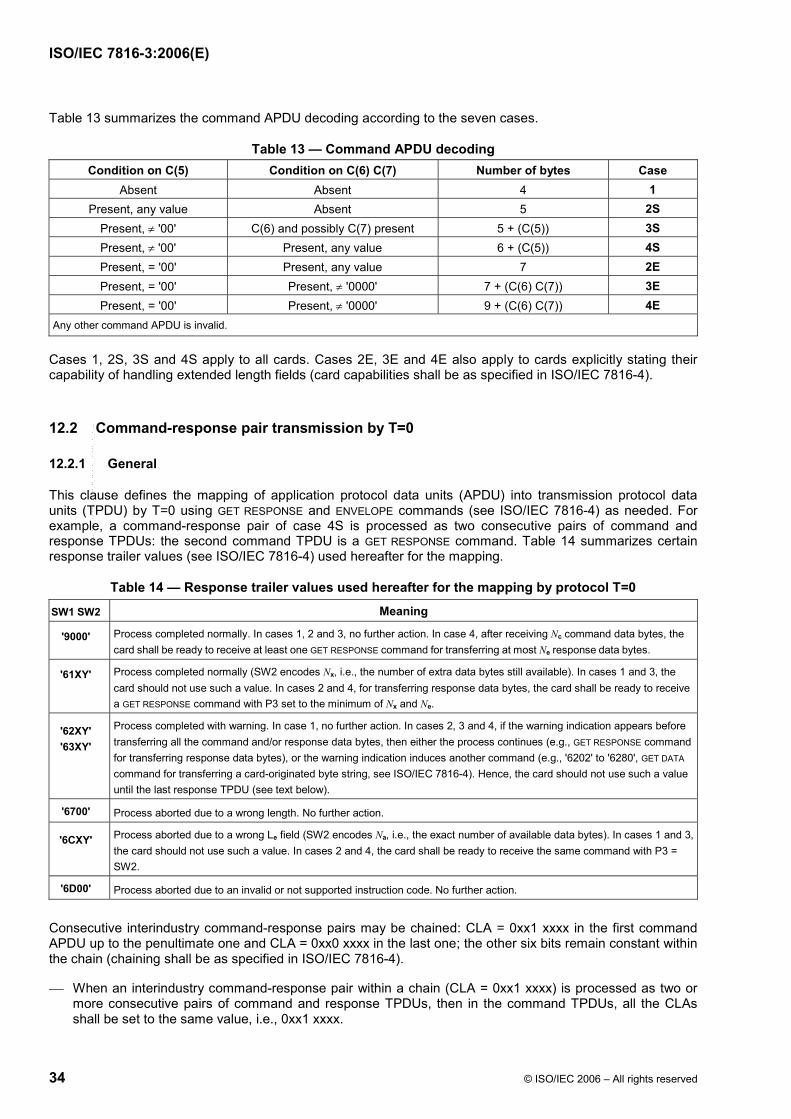
ISO/IEC 7816-3:2006(E)
34 © ISO/IEC 2006 – All rights reserved
Table 13 summarizes the command APDU decoding according to the seven cases.
Table 13 — Command APDU decoding Condition on C(5) Condition on C(6) C(7) Number of bytes Case
Absent Absent 4 1 Present, any value Absent 5 2S
Present, ≠ '00' C(6) and possibly C(7) present 5 + (C(5)) 3S Present, ≠ '00' Present, any value 6 + (C(5)) 4S Present, = '00' Present, any value 7 2E Present, = '00' Present, ≠ '0000' 7 + (C(6) C(7)) 3E Present, = '00' Present, ≠ '0000' 9 + (C(6) C(7)) 4E
Any other command APDU is invalid. Cases 1, 2S, 3S and 4S apply to all cards. Cases 2E, 3E and 4E also apply to cards explicitly stating their capability of handling extended length fields (card capabilities shall be as specified in ISO/IEC 7816-4).
12.2 Command-response pair transmission by T=0
12.2.1 General
This clause defines the mapping of application protocol data units (APDU) into transmission protocol data units (TPDU) by T=0 using GET RESPONSE and ENVELOPE commands (see ISO/IEC 7816-4) as needed. For example, a command-response pair of case 4S is processed as two consecutive pairs of command and response TPDUs: the second command TPDU is a GET RESPONSE command. Table 14 summarizes certain response trailer values (see ISO/IEC 7816-4) used hereafter for the mapping.
Table 14 — Response trailer values used hereafter for the mapping by protocol T=0
SW1 SW2 Meaning
'9000' Process completed normally. In cases 1, 2 and 3, no further action. In case 4, after receiving Nc command data bytes, the
card shall be ready to receive at least one GET RESPONSE command for transferring at most Ne response data bytes.
'61XY' Process completed normally (SW2 encodes Nx, i.e., the number of extra data bytes still available). In cases 1 and 3, the card should not use such a value. In cases 2 and 4, for transferring response data bytes, the card shall be ready to receive a GET RESPONSE command with P3 set to the minimum of Nx and Ne.
'62XY' '63XY'
Process completed with warning. In case 1, no further action. In cases 2, 3 and 4, if the warning indication appears before transferring all the command and/or response data bytes, then either the process continues (e.g., GET RESPONSE command for transferring response data bytes), or the warning indication induces another command (e.g., '6202' to '6280', GET DATA command for transferring a card-originated byte string, see ISO/IEC 7816-4). Hence, the card should not use such a value until the last response TPDU (see text below).
'6700' Process aborted due to a wrong length. No further action.
'6CXY' Process aborted due to a wrong Le field (SW2 encodes Na, i.e., the exact number of available data bytes). In cases 1 and 3, the card should not use such a value. In cases 2 and 4, the card shall be ready to receive the same command with P3 = SW2.
'6D00' Process aborted due to an invalid or not supported instruction code. No further action.
Consecutive interindustry command-response pairs may be chained: CLA = 0xx1 xxxx in the first command APDU up to the penultimate one and CLA = 0xx0 xxxx in the last one; the other six bits remain constant within the chain (chaining shall be as specified in ISO/IEC 7816-4).
⎯ When an interindustry command-response pair within a chain (CLA = 0xx1 xxxx) is processed as two or more consecutive pairs of command and response TPDUs, then in the command TPDUs, all the CLAs shall be set to the same value, i.e., 0xx1 xxxx.
--`,``,``,,,`,```,`,`,,`,,`,,``-`-`,,`,,`,`,,`---
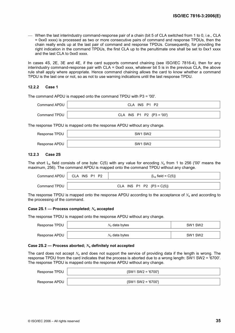
ISO/IEC 7816-3:2006(E)
© ISO/IEC 2006 – All rights reserved 35
⎯ When the last interindustry command-response pair of a chain (bit 5 of CLA switched from 1 to 0, i.e., CLA = 0xx0 xxxx) is processed as two or more consecutive pairs of command and response TPDUs, then the chain really ends up at the last pair of command and response TPDUs. Consequently, for providing the right indication in the command TPDUs, the first CLA up to the penultimate one shall be set to 0xx1 xxxx and the last CLA to 0xx0 xxxx.
In cases 4S, 2E, 3E and 4E, if the card supports command chaining (see ISO/IEC 7816-4), then for any interindustry command-response pair with CLA = 0xx0 xxxx, whatever bit 5 is in the previous CLA, the above rule shall apply where appropriate. Hence command chaining allows the card to know whether a command TPDU is the last one or not, so as not to use warning indications until the last response TPDU.
12.2.2 Case 1
The command APDU is mapped onto the command TPDU with P3 = '00'.
Command APDU CLA INS P1 P2
Command TPDU CLA INS P1 P2 P3 = '00'
The response TPDU is mapped onto the response APDU without any change.
Response TPDU SW1 SW2
Response APDU SW1 SW2
12.2.3 Case 2S
The short Le field consists of one byte: C(5) with any value for encoding Ne from 1 to 256 ('00' means the maximum, 256). The command APDU is mapped onto the command TPDU without any change.
Command APDU CLA INS P1 P2 Le field = C(5)
Command TPDU CLA INS P1 P2 P3 = C(5)
The response TPDU is mapped onto the response APDU according to the acceptance of Ne and according to the processing of the command.
Case 2S.1 — Process completed; Ne accepted
The response TPDU is mapped onto the response APDU without any change.
Response TPDU Ne data bytes SW1 SW2
Response APDU Ne data bytes SW1 SW2
Case 2S.2 — Process aborted; Ne definitely not accepted
The card does not accept Ne and does not support the service of providing data if the length is wrong. The response TPDU from the card indicates that the process is aborted due to a wrong length: SW1 SW2 = '6700'. The response TPDU is mapped onto the response APDU without any change.
Response TPDU SW1 SW2 = '6700'
Response APDU SW1 SW2 = '6700'
ISO/IEC 7816-3:2006(E)
36 © ISO/IEC 2006 – All rights reserved
Case 2S.3 — Process aborted; Ne not accepted, Na indicated
The card does not accept Ne and the response TPDU from the card indicates that the process is aborted: SW1 = '6C' (wrong length) and SW2 with any value for encoding Na from 1 to 256 ('00' means 256), namely, the exact number of available data bytes.
Response TPDU SW1 = '6C' SW2
The card shall be ready to receive the same command TPDU with P3 = SW2.
Command TPDU CLA INS P1 P2 P3 = SW2
The response TPDU consists of Na data bytes followed by SW1 SW2.
Response TPDU Na data bytes SW1 SW2
⎯ If Na≤ Ne, then the response TPDU is mapped onto the response APDU without any change.
Response APDU Na (≤ Ne) data bytes SW1 SW2
⎯ If Na > Ne, then the response TPDU is mapped onto the response APDU by keeping only the first Ne bytes of the response APDU and the two status bytes SW1 SW2.
Response APDU Ne (< Na) data bytes SW1 SW2
Case 2S.4 — SW1 SW2 = '9XYZ', except for '9000'
The response TPDU is mapped onto the response APDU without any change.
12.2.4 Case 3S
The short Lc field consists of one byte: C(5) ≠ '00' for encoding Nc from 1 to 255. The command APDU is mapped onto the command TPDU without any change.
Command APDU CLA INS P1 P2 Lc field = C(5) Nc data bytes
Command TPDU CLA INS P1 P2 P3 = C(5) Nc data bytes
The response TPDU is mapped onto the response APDU without any change.
Response TPDU SW1 SW2
Response APDU SW1 SW2
12.2.5 Case 4S
The short Lc field consists of one byte: C(5) ≠ '00' for encoding Nc from 1 to 255. The short Le field consists of one byte: C(n) with any value for encoding Ne from 1 to 256 ('00' means the maximum, 256). The command APDU is mapped onto the command TPDU by cutting off the Le field, i.e., C(n).
Command APDU CLA INS P1 P2 Lc field = C(5) Nc data bytes Le field = C(n)
Command TPDU CLA INS P1 P2 P3 = C(5) Nc data bytes
--`,``,``,,,`,```,`,`,,`,,`,,``-`-`,,`,,`,`,,`---
ISO/IEC 7816-3:2006(E)
© ISO/IEC 2006 – All rights reserved 37
Case 4S.1 — Process aborted
The first response TPDU from the card indicates that the process is aborted: SW1 = '6X', except for '61', '62' and '63'. The response TPDU is mapped onto the response APDU without any change.
Response TPDU SW1 = '6X' except for '61', '62' and '63' SW2
Response APDU SW1 = '6X' except for '61', '62' and '63' SW2 Case 4S.2 — Process completed
The first response TPDU from the card indicates that the process is completed: SW1 SW2 = '9000'. The card shall be ready to receive a GET RESPONSE command TPDU with P3 = C(n).
Command TPDU CLA INS = GET RESPONSE P1 P2 P3 = C(n)
Depending on the second response TPDU from the card, the process shall continue according to cases 2S.1, 2S.2, 2S.3 and 2S.4 above.
Case 4S.3 — Process completed with information added
The first response TPDU from the card indicates that the process is completed and the card gives information: SW1 = '61' and SW2 with any value for encoding Nx from 1 to 256 ('00' means 256), namely, the number of extra data bytes still available. The card shall be ready to receive a GET RESPONSE command TPDU with P3 set to the minimum of Nx and Ne.
Command TPDU CLA INS = GET RESPONSE P1 P2 P3 = min(Ne, Nx)
The second response TPDU is mapped onto the response APDU without any change.
Response TPDU P3 data bytes SW1 SW2
Response APDU P3 data bytes SW1 SW2
Case 4S.4 — SW1 SW2 = either '62XY' or '63XY' or '9XYZ', except for '9000'
The response TPDU is mapped onto the response APDU without any change.
NOTE In case 4S, the use of '62XY' and '63XY' is not recommended in the first response TPDU.
12.2.6 Case 2E
The extended Le field consists of three bytes: C(5) C(6) C(7); C(5) = '00' and C(6) C(7) has any value for encoding Ne from 1 to 65 536 ('0000' means the maximum, 65 536).
Command APDU CLA INS P1 P2 Le field = C(5) C(6) C(7)
Case 2E.1 — Ne ≤ 256, C(5) = '00', C(6) C(7) from '0001' to '0100'
As Ne is from 1 to 256, the command APDU shall be mapped onto the command TPDU with P3 = C(7). The process shall continue according to case 2S.
Command TPDU CLA INS P1 P2 P3 = C(7)
Case 2E.2 — Ne > 256, C(5) = '00', C(6) C(7) = either '0000' or from '0101' to 'FFFF'
As Ne > 256, the command APDU shall be mapped onto the command TPDU with P3 = '00'.
Command TPDU CLA INS P1 P2 P3 = '00'
--`,``,``,,,`,```,`,`,,`,,`,,``-`-`,,`,,`,`,,`---
ISO/IEC 7816-3:2006(E)
38 © ISO/IEC 2006 – All rights reserved
a) If the first response TPDU from the card indicates that the process is aborted due to a wrong length (SW1 SW2 = '6700'), then the response TPDU shall be mapped onto the response APDU without any change.
Response TPDU SW1 SW2 = '6700'
Response APDU SW1 SW2 = '6700'
b) If the first response TPDU from the card indicates that the process is aborted due to a wrong length and the card gives information: SW1 = '6C' and SW2 with any value for encoding Na from 1 to 256 ('00' means 256), namely, the exact number of available data bytes, then the process shall be completed as described in case 2S.3.
c) If the first response TPDU is 256 data bytes followed by SW1 SW2 = '9000', this means that the card has no more than 256 data bytes, and/or does not support the GET RESPONSE command. The response TPDU shall then be mapped onto the response APDU without any change.
Response TPDU 256 data bytes SW1 SW2 = '9000'
Response APDU 256 data bytes SW1 SW2 = '9000'
d) If the first or subsequent response TPDU from the card is SW1 = '61', then SW2 with any value encodes Nx from 1 to 256 ('00' means 256), namely, the number of extra data bytes still available. The number of remaining data bytes to be retrieved from the card is Nm = Ne minus the number of data bytes received in the previous response TPDUs.
• If Nm = 0, then the response APDU shall be the concatenation of the data bytes of all received response TPDUs together with the trailer of the last received response TPDU.
• If Nm > 0, then the card shall be ready receive a GET RESPONSE command TPDU with P3 set to the minimum of Nx and Nm. The corresponding response TPDU from the card shall be processed
— according to case d), if SW1 = '61', — as above when Nm is zero, if SW1 SW2 = '9000'.
12.2.7 Case 3E
The extended Lc field consists of three bytes: C(5) C(6) C(7); C(5) = '00' and C(6) C(7) ≠ '0000' for encoding Nc from 1 to 65 535.
Command APDU CLA INS P1 P2 Lc field = C(5) C(6) C(7) Nc data bytes
Case 3E.1 — Nc from 1 to 255, C(5) C(6) = '0000', C(7) ≠ '00'
As Nc is from 1 to 255, the command APDU is mapped onto the command TPDU with P3 = C(7).
Command TPDU CLA INS P1 P2 P3 = C(7) Nc data bytes
The response TPDU is mapped onto the response APDU without any change.
Response TPDU SW1 SW2
Response APDU SW1 SW2
Case 3E.2 — Nc > 255, C(5) = '00', C(6) ≠ '00', C(7) any value
The command APDU shall be split into consecutive segments of less than 256 bytes transmitted into the data bytes of consecutive ENVELOPE command TPDUs. The absence of data bytes means “end of data string”.
Command TPDU CLA INS = ENVELOPE P1 P2 P3 P3 bytes
ISO/IEC 7816-3:2006(E)
© ISO/IEC 2006 – All rights reserved 39
⎯ If the first response TPDU from the card indicates that the card does not support the ENVELOPE command (SW1 SW2 = '6D00'), the TPDU shall be mapped onto the response APDU without any change.
Response TPDU SW1 SW2 = '6D00'
Response APDU SW1 SW2 = '6D00'
⎯ If the first response TPDU from the card indicates that the card does support the ENVELOPE command (SW1 SW2 = '9000'), then the card shall be ready to receive further ENVELOPE commands as needed.
Response TPDU SW1 SW2 = '9000'
Command TPDU CLA INS = ENVELOPE P1 P2 P3 P3 bytes
⎯ The response TPDU corresponding to the last ENVELOPE command is mapped onto the response APDU without any change.
Response TPDU SW1 SW2
Response APDU SW1 SW2
12.2.8 Case 4E
The extended Lc field consists of three bytes: C(5) C(6) C(7); C(5) = '00' and C(6) C(7) ≠ '0000' for encoding Nc from 1 to 65 535. The extended Le field consists of two bytes: C(n–1) C(n) with any value for encoding Ne from 1 to 65 536 ('0000' means the maximum, 65 536).
Command APDU CLA INS P1 P2 Lc field = C(5) C(6) C(7) Nc data bytes Le field = C(n−1) C(n)
Case 4E.1 — Nc < 256, C(5) C(6) = '0000', C(7) ≠ '00'
As Nc is from 1 to 255, the command APDU is mapped onto the command TPDU with P3 = C(7) and by appending the Nc data bytes. The Le field, i.e., C(n–1) C(n), is cut off.
Command TPDU CLA INS P1 P2 P3 = C(7) Nc data bytes
a) If SW1 = '6X' except for '61', '62' or '63' in the first response TPDU from the card, then the response TPDU is mapped onto the response APDU without any change.
Response TPDU SW1 = '6X' except for '61', '62' or '63' SW2
Response APDU SW1 = '6X' except for '61', '62' or '63' SW2
b) If SW1 SW2 = '9000' in the first response TPDU from the card, then
• If Ne ≤ 256, i.e., C(n–1) C(n) from '0001' to '0100', then the card shall be ready to receive a GET RESPONSE command TPDU with P3 = C(n). The subsequent process shall be according to cases 2S.1, 2S.2, 2S.3 and 2S.4 above.
• If Ne > 256, i.e., C(n–1) C(n) = either '0000' or > '0100', then the card shall be ready to receive a GET RESPONSE command TPDU with P3 = '00'. The subsequent process shall be according to case 2E.2 above.
c) If SW1 = '61' in the first response TPDU from the card, then the process shall continue according to case 2E.2 d) above.
d) If SW1 SW2 = '62XY' or '63XY' or '9XYZ', except for '9000', in the first response TPDU from the card, then the response TPDU is mapped onto the response APDU without any change.
NOTE In case 4E, the use of '62XY' and '63XY' is not recommended until the last response TPDU.
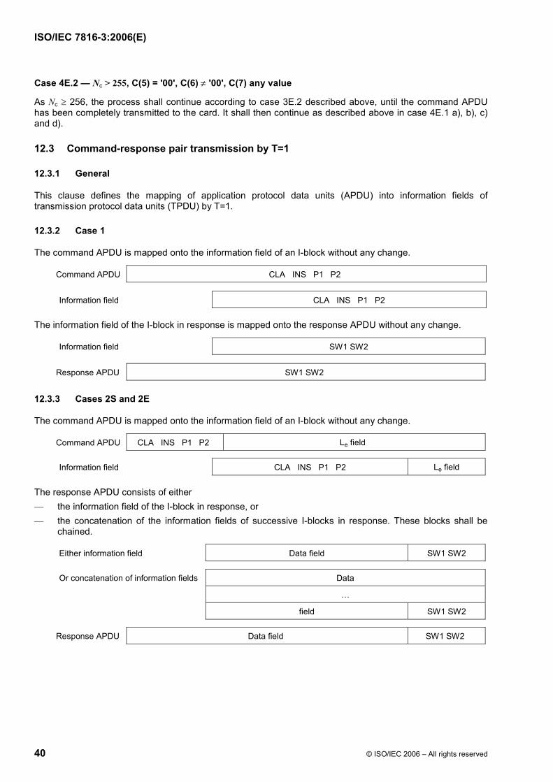
ISO/IEC 7816-3:2006(E)
40 © ISO/IEC 2006 – All rights reserved
Case 4E.2 — Nc > 255, C(5) = '00', C(6) ≠ '00', C(7) any value
As Nc ≥ 256, the process shall continue according to case 3E.2 described above, until the command APDU has been completely transmitted to the card. It shall then continue as described above in case 4E.1 a), b), c) and d).
12.3 Command-response pair transmission by T=1
12.3.1 General
This clause defines the mapping of application protocol data units (APDU) into information fields of transmission protocol data units (TPDU) by T=1.
12.3.2 Case 1
The command APDU is mapped onto the information field of an I-block without any change.
Command APDU CLA INS P1 P2
Information field CLA INS P1 P2
The information field of the I-block in response is mapped onto the response APDU without any change.
Information field SW1 SW2
Response APDU SW1 SW2
12.3.3 Cases 2S and 2E
The command APDU is mapped onto the information field of an I-block without any change.
Command APDU CLA INS P1 P2 Le field
Information field CLA INS P1 P2 Le field
The response APDU consists of either — the information field of the I-block in response, or — the concatenation of the information fields of successive I-blocks in response. These blocks shall be
chained.
Either information field Data field SW1 SW2
Or concatenation of information fields Data
…
field SW1 SW2
Response APDU Data field SW1 SW2
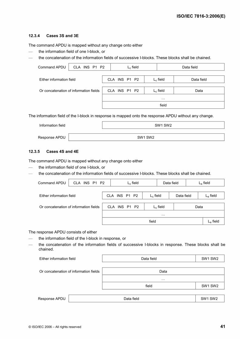
ISO/IEC 7816-3:2006(E)
© ISO/IEC 2006 – All rights reserved 41
12.3.4 Cases 3S and 3E
The command APDU is mapped without any change onto either — the information field of one I-block, or — the concatenation of the information fields of successive I-blocks. These blocks shall be chained.
Command APDU CLA INS P1 P2 Lc field Data field
Either information field CLA INS P1 P2 Lc field Data field
Or concatenation of information fields CLA INS P1 P2 Lc field Data
…
field
The information field of the I-block in response is mapped onto the response APDU without any change.
Information field SW1 SW2
Response APDU SW1 SW2
12.3.5 Cases 4S and 4E
The command APDU is mapped without any change onto either — the information field of one I-block, or — the concatenation of the information fields of successive I-blocks. These blocks shall be chained.
Command APDU CLA INS P1 P2 Lc field Data field Le field
Either information field CLA INS P1 P2 Lc field Data field Le field
Or concatenation of information fields CLA INS P1 P2 Lc field Data
…
field Le field
The response APDU consists of either — the information field of the I-block in response, or — the concatenation of the information fields of successive I-blocks in response. These blocks shall be
chained.
Either information field Data field SW1 SW2
Or concatenation of information fields Data
…
field SW1 SW2
Response APDU Data field SW1 SW2
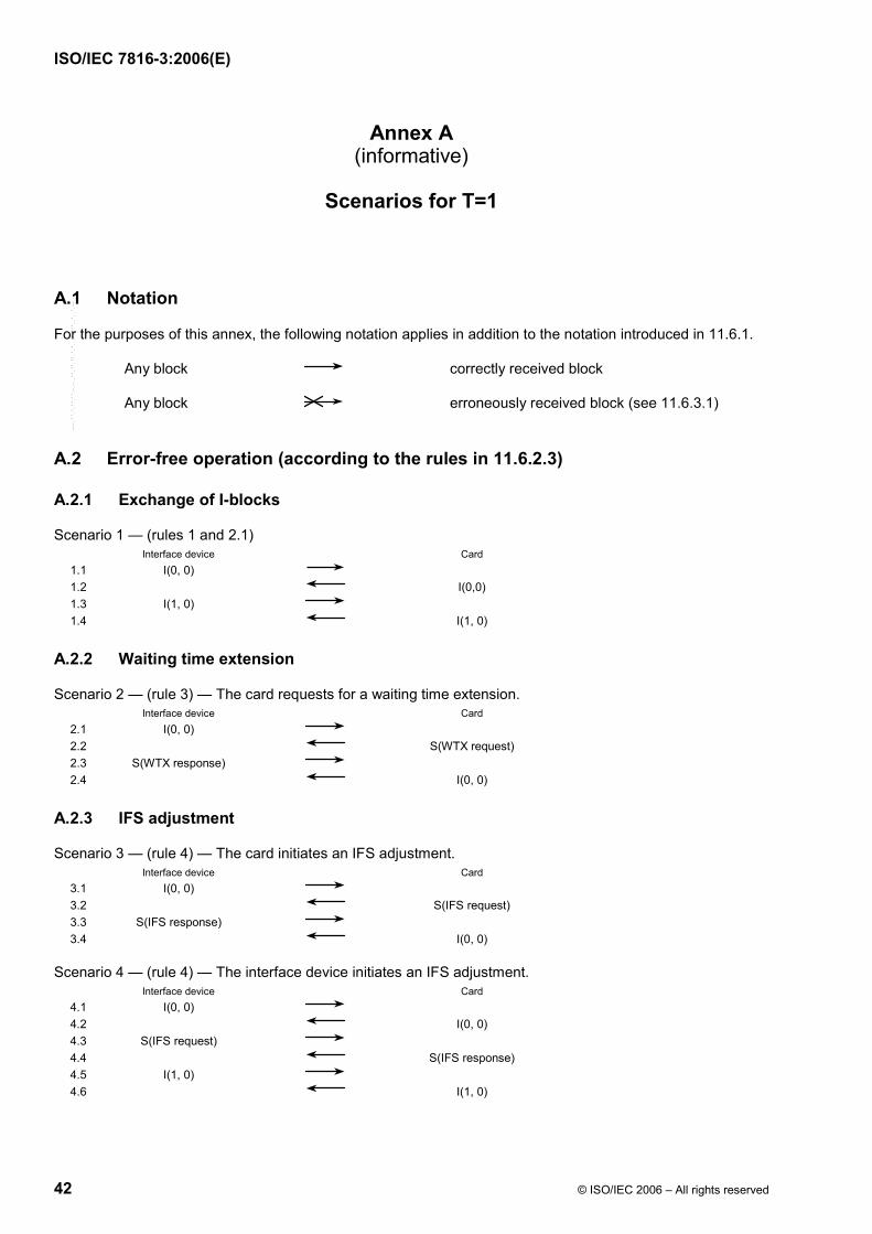
ISO/IEC 7816-3:2006(E)
42 © ISO/IEC 2006 – All rights reserved
Annex A (informative)
Scenarios for T=1
A.1 Notation
For the purposes of this annex, the following notation applies in addition to the notation introduced in 11.6.1.
Any block correctly received block
Any block erroneously received block (see 11.6.3.1)
A.2 Error-free operation (according to the rules in 11.6.2.3)
A.2.1 Exchange of I-blocks
Scenario 1 — (rules 1 and 2.1) Interface device Card 1.1 I(0, 0) 1.2 I(0,0) 1.3 I(1, 0) 1.4 I(1, 0)
A.2.2 Waiting time extension
Scenario 2 — (rule 3) — The card requests for a waiting time extension. Interface device Card 2.1 I(0, 0) 2.2 S(WTX request) 2.3 S(WTX response) 2.4 I(0, 0)
A.2.3 IFS adjustment
Scenario 3 — (rule 4) — The card initiates an IFS adjustment. Interface device Card 3.1 I(0, 0) 3.2 S(IFS request) 3.3 S(IFS response) 3.4 I(0, 0)
Scenario 4 — (rule 4) — The interface device initiates an IFS adjustment. Interface device Card 4.1 I(0, 0) 4.2 I(0, 0) 4.3 S(IFS request) 4.4 S(IFS response) 4.5 I(1, 0) 4.6 I(1, 0)
--`,``,``,,,`,```,`,`,,`,,`,,``-`-`,,`,,`,`,,`---
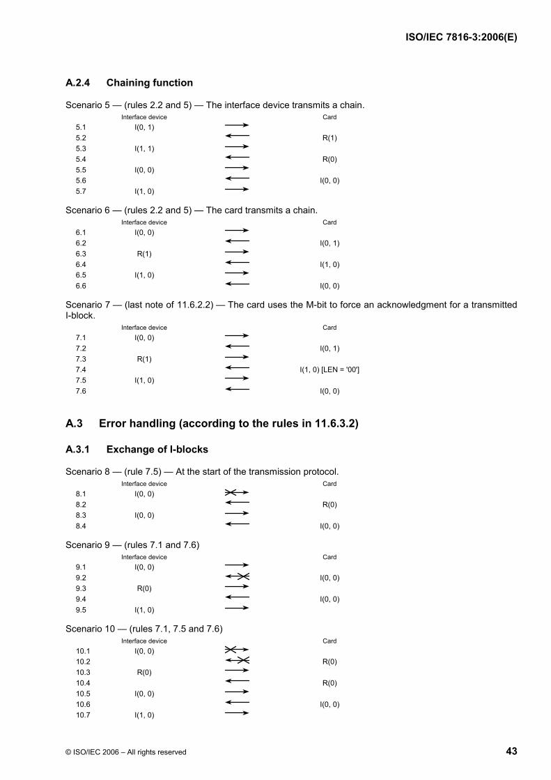
ISO/IEC 7816-3:2006(E)
© ISO/IEC 2006 – All rights reserved 43
A.2.4 Chaining function
Scenario 5 — (rules 2.2 and 5) — The interface device transmits a chain. Interface device Card 5.1 I(0, 1) 5.2 R(1) 5.3 I(1, 1) 5.4 R(0) 5.5 I(0, 0) 5.6 I(0, 0) 5.7 I(1, 0)
Scenario 6 — (rules 2.2 and 5) — The card transmits a chain. Interface device Card 6.1 I(0, 0) 6.2 I(0, 1) 6.3 R(1) 6.4 I(1, 0) 6.5 I(1, 0) 6.6 I(0, 0)
Scenario 7 — (last note of 11.6.2.2) — The card uses the M-bit to force an acknowledgment for a transmitted I-block. Interface device Card 7.1 I(0, 0) 7.2 I(0, 1) 7.3 R(1) 7.4 I(1, 0) [LEN = '00'] 7.5 I(1, 0) 7.6 I(0, 0)
A.3 Error handling (according to the rules in 11.6.3.2)
A.3.1 Exchange of I-blocks
Scenario 8 — (rule 7.5) — At the start of the transmission protocol. Interface device Card 8.1 I(0, 0) 8.2 R(0) 8.3 I(0, 0) 8.4 I(0, 0)
Scenario 9 — (rules 7.1 and 7.6) Interface device Card 9.1 I(0, 0) 9.2 I(0, 0) 9.3 R(0) 9.4 I(0, 0) 9.5 I(1, 0)
Scenario 10 — (rules 7.1, 7.5 and 7.6) Interface device Card 10.1 I(0, 0) 10.2 R(0) 10.3 R(0) 10.4 R(0) 10.5 I(0, 0) 10.6 I(0, 0) 10.7 I(1, 0)
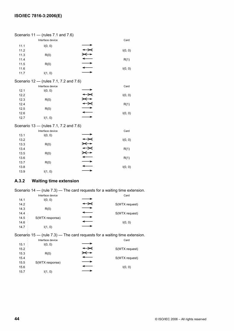
ISO/IEC 7816-3:2006(E)
44 © ISO/IEC 2006 – All rights reserved
Scenario 11 — (rules 7.1 and 7.6) Interface device Card
11.1 I(0, 0) 11.2 I(0, 0) 11.3 R(0) 11.4 R(1) 11.5 R(0) 11.6 I(0, 0) 11.7 I(1, 0)
Scenario 12 — (rules 7.1, 7.2 and 7.6) Interface device Card 12.1 I(0, 0) 12.2 I(0, 0) 12.3 R(0) 12.4 R(1) 12.5 R(0) 12.6 I(0, 0) 12.7 I(1, 0)
Scenario 13 — (rules 7.1, 7.2 and 7.6) Interface device Card 13.1 I(0, 0) 13.2 I(0, 0) 13.3 R(0) 13.4 R(1) 13.5 R(0) 13.6 R(1) 13.7 R(0) 13.8 I(0, 0) 13.9 I(1, 0)
A.3.2 Waiting time extension
Scenario 14 — (rule 7.3) — The card requests for a waiting time extension. Interface device Card 14.1 I(0, 0) 14.2 S(WTX request) 14.3 R(0) 14.4 S(WTX request) 14.5 S(WTX response) 14.6 I(0, 0) 14.7 I(1, 0)
Scenario 15 — (rule 7.3) — The card requests for a waiting time extension. Interface device Card 15.1 I(0, 0) 15.2 S(WTX request) 15.3 R(0) 15.4 S(WTX request) 15.5 S(WTX response) 15.6 I(0, 0) 15.7 I(1, 0)
--`,``,``,,,`,```,`,`,,`,,`,,``-`-`,,`,,`,`,,`---
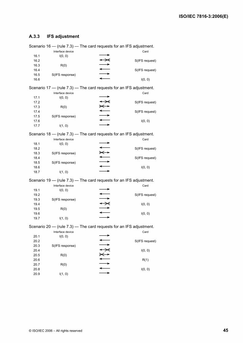
ISO/IEC 7816-3:2006(E)
© ISO/IEC 2006 – All rights reserved 45
A.3.3 IFS adjustment
Scenario 16 — (rule 7.3) — The card requests for an IFS adjustment. Interface device Card 16.1 I(0, 0) 16.2 S(IFS request) 16.3 R(0) 16.4 S(IFS request) 16.5 S(IFS response) 16.6 I(0, 0)
Scenario 17 — (rule 7.3) — The card requests for an IFS adjustment. Interface device Card 17.1 I(0, 0) 17.2 S(IFS request) 17.3 R(0) 17.4 S(IFS request) 17.5 S(IFS response) 17.6 I(0, 0) 17.7 I(1, 0)
Scenario 18 — (rule 7.3) — The card requests for an IFS adjustment. Interface device Card 18.1 I(0, 0) 18.2 S(IFS request) 18.3 S(IFS response) 18.4 S(IFS request) 18.5 S(IFS response) 18.6 I(0, 0) 18.7 I(1, 0)
Scenario 19 — (rule 7.3) — The card requests for an IFS adjustment. Interface device Card 19.1 I(0, 0) 19.2 S(IFS request) 19.3 S(IFS response) 19.4 I(0, 0) 19.5 R(0) 19.6 I(0, 0) 19.7 I(1, 0)
Scenario 20 — (rule 7.3) — The card requests for an IFS adjustment. Interface device Card 20.1 I(0, 0) 20.2 S(IFS request) 20.3 S(IFS response) 20.4 I(0, 0) 20.5 R(0) 20.6 R(1) 20.7 R(0) 20.8 I(0, 0) 20.9 I(1, 0)
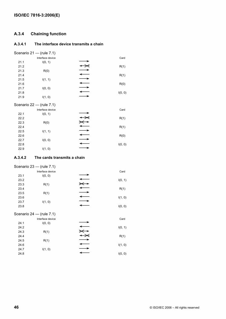
ISO/IEC 7816-3:2006(E)
46 © ISO/IEC 2006 – All rights reserved
A.3.4 Chaining function
A.3.4.1 The interface device transmits a chain
Scenario 21 — (rule 7.1) Interface device Card 21.1 I(0, 1) 21.2 R(1) 21.3 R(0) 21.4 R(1) 21.5 I(1, 1) 21.6 R(0) 21.7 I(0, 0) 21.8 I(0, 0) 21.9 I(1, 0)
Scenario 22 — (rule 7.1) Interface device Card 22.1 I(0, 1) 22.2 R(1) 22.3 R(0) 22.4 R(1) 22.5 I(1, 1) 22.6 R(0) 22.7 I(0, 0) 22.8 I(0, 0) 22.9 I(1, 0)
A.3.4.2 The cards transmits a chain
Scenario 23 — (rule 7.1) Interface device Card 23.1 I(0, 0) 23.2 I(0, 1) 23.3 R(1) 23.4 R(1) 23.5 R(1) 23.6 I(1, 0) 23.7 I(1, 0) 23.8 I(0, 0)
Scenario 24 — (rule 7.1) Interface device Card 24.1 I(0, 0) 24.2 I(0, 1) 24.3 R(1) 24.4 R(1) 24.5 R(1) 24.6 I(1, 0) 24.7 I(1, 0) 24.8 I(0, 0)
--`,``,``,,,`,```,`,`,,`,,`,,``-`-`,,`,,`,`,,`---
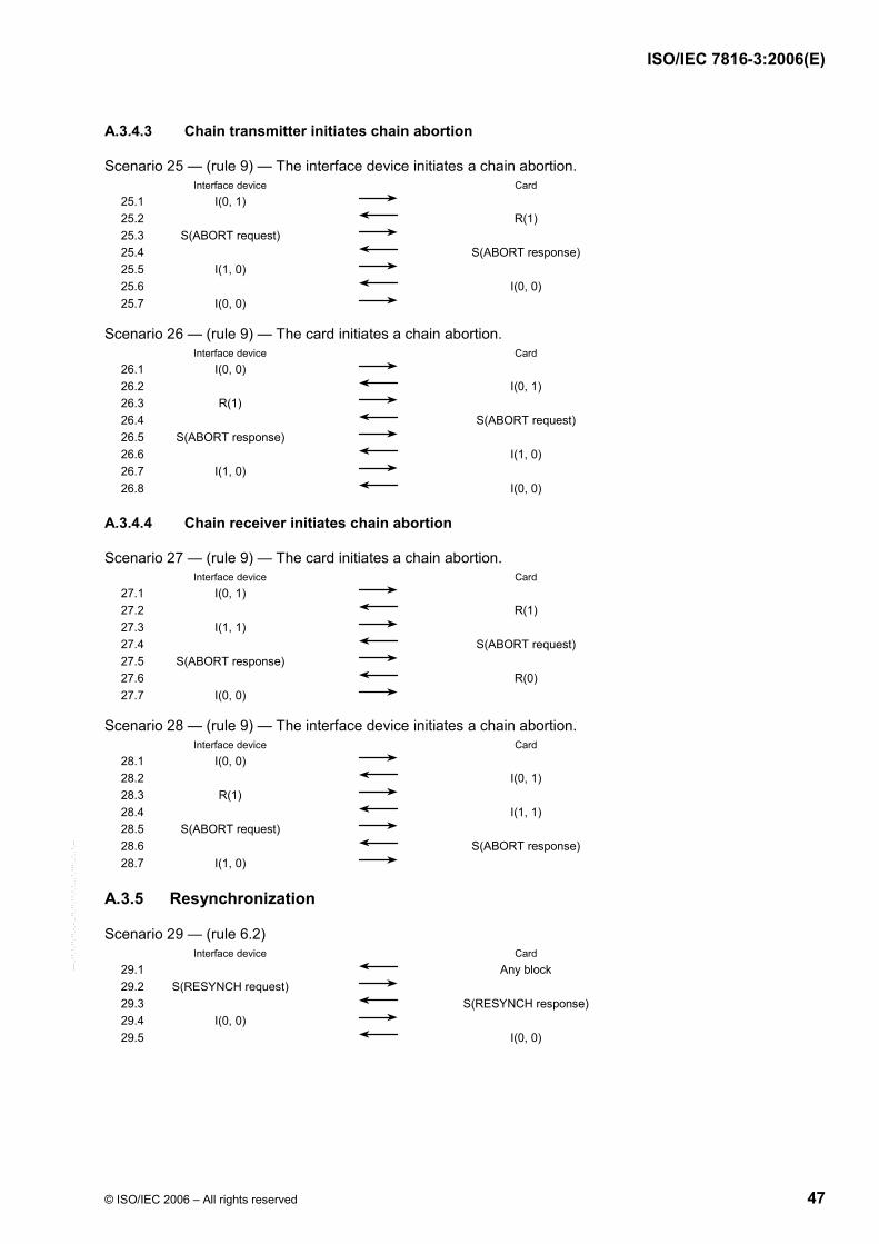
ISO/IEC 7816-3:2006(E)
© ISO/IEC 2006 – All rights reserved 47
A.3.4.3 Chain transmitter initiates chain abortion
Scenario 25 — (rule 9) — The interface device initiates a chain abortion. Interface device Card 25.1 I(0, 1) 25.2 R(1) 25.3 S(ABORT request) 25.4 S(ABORT response) 25.5 I(1, 0) 25.6 I(0, 0) 25.7 I(0, 0)
Scenario 26 — (rule 9) — The card initiates a chain abortion. Interface device Card 26.1 I(0, 0) 26.2 I(0, 1) 26.3 R(1) 26.4 S(ABORT request) 26.5 S(ABORT response) 26.6 I(1, 0) 26.7 I(1, 0) 26.8 I(0, 0)
A.3.4.4 Chain receiver initiates chain abortion
Scenario 27 — (rule 9) — The card initiates a chain abortion. Interface device Card 27.1 I(0, 1) 27.2 R(1) 27.3 I(1, 1) 27.4 S(ABORT request) 27.5 S(ABORT response) 27.6 R(0) 27.7 I(0, 0)
Scenario 28 — (rule 9) — The interface device initiates a chain abortion. Interface device Card 28.1 I(0, 0) 28.2 I(0, 1) 28.3 R(1) 28.4 I(1, 1) 28.5 S(ABORT request) 28.6 S(ABORT response) 28.7 I(1, 0)
A.3.5 Resynchronization
Scenario 29 — (rule 6.2) Interface device Card 29.1 Any block 29.2 S(RESYNCH request) 29.3 S(RESYNCH response) 29.4 I(0, 0) 29.5 I(0, 0)
--`,``,``,,,`,```,`,`,,`,,`,,``-`-`,,`,,`,`,,`---
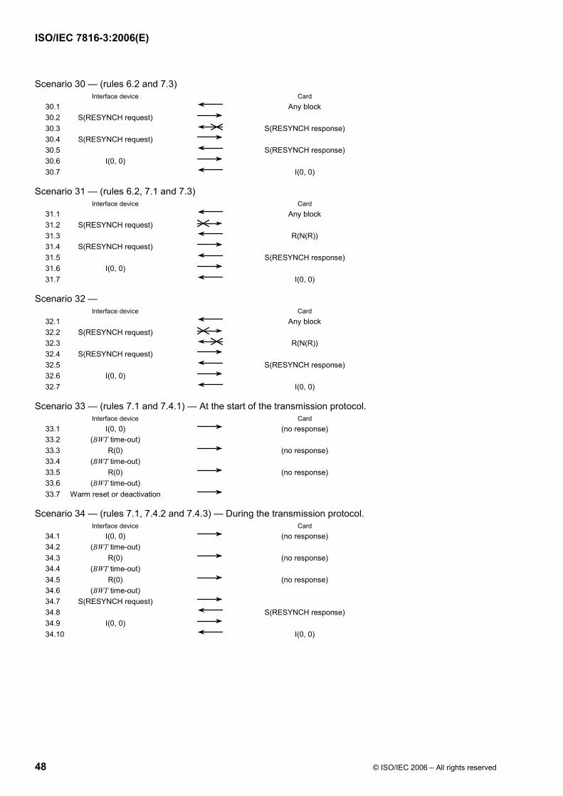
ISO/IEC 7816-3:2006(E)
48 © ISO/IEC 2006 – All rights reserved
Scenario 30 — (rules 6.2 and 7.3) Interface device Card 30.1 Any block 30.2 S(RESYNCH request) 30.3 S(RESYNCH response) 30.4 S(RESYNCH request) 30.5 S(RESYNCH response) 30.6 I(0, 0) 30.7 I(0, 0)
Scenario 31 — (rules 6.2, 7.1 and 7.3) Interface device Card 31.1 Any block 31.2 S(RESYNCH request) 31.3 R(N(R)) 31.4 S(RESYNCH request) 31.5 S(RESYNCH response) 31.6 I(0, 0) 31.7 I(0, 0)
Scenario 32 — Interface device Card 32.1 Any block 32.2 S(RESYNCH request) 32.3 R(N(R)) 32.4 S(RESYNCH request) 32.5 S(RESYNCH response) 32.6 I(0, 0) 32.7 I(0, 0)
Scenario 33 — (rules 7.1 and 7.4.1) — At the start of the transmission protocol. Interface device Card 33.1 I(0, 0) (no response) 33.2 (BWT time-out) 33.3 R(0) (no response) 33.4 (BWT time-out) 33.5 R(0) (no response) 33.6 (BWT time-out) 33.7 Warm reset or deactivation
Scenario 34 — (rules 7.1, 7.4.2 and 7.4.3) — During the transmission protocol. Interface device Card 34.1 I(0, 0) (no response) 34.2 (BWT time-out) 34.3 R(0) (no response) 34.4 (BWT time-out) 34.5 R(0) (no response) 34.6 (BWT time-out) 34.7 S(RESYNCH request) 34.8 S(RESYNCH response) 34.9 I(0, 0) 34.10 I(0, 0)
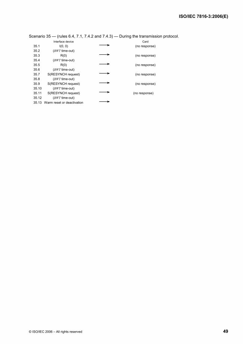
ISO/IEC 7816-3:2006(E)
© ISO/IEC 2006 – All rights reserved 49
Scenario 35 — (rules 6.4, 7.1, 7.4.2 and 7.4.3) — During the transmission protocol. Interface device Card 35.1 I(0, 0) (no response) 35.2 (BWT time-out) 35.3 R(0) (no response) 35.4 (BWT time-out) 35.5 R(0) (no response) 35.6 (BWT time-out) 35.7 S(RESYNCH request) (no response) 35.8 (BWT time-out) 35.9 S(RESYNCH request) (no response) 35.10 (BWT time-out) 35.11 S(RESYNCH request) (no response) 35.12 (BWT time-out) 35.13 Warm reset or deactivation
ISO/IEC 7816-3:2006(E)
50 © ISO/IEC 2006 – All rights reserved
Bibliography
[1] ISO 31 (all parts), Quantities and units 1)
[2] ISO/IEC 7810:2003, Identification cards — Physical characteristics
[3] ISO/IEC 10536 (all parts), Identification cards — Contactless integrated circuit(s) cards — Close-coupled cards
[4] ISO/IEC 13239:2002, Information technology — Telecommunications and information exchange between systems — High-level data link control (HDLC) procedures
[5] ISO/IEC 14443 (all parts), Identification cards — Contactless integrated circuit(s) cards — Proximity cards
[6] ISO/IEC 15693 (all parts), Identification cards — Contactless integrated circuit(s) cards — Vicinity cards
1) Published as a compilation in ISO Standards Handbook, Quantities and units.
--`,``,``,,,`,```,`,`,,`,,`,,``-`-`,,`,,`,`,,`---


ISO/IEC 7816-3:2006(E)
ICS 35.240.15 Price based on 50 pages
© ISO/IEC 2006 – All rights reserved