ideal tx-line fundamentals -...
TRANSCRIPT

Ideal Tx-Line Fundamentals
吳瑞北
Rm. 340, Department of Electrical Engineering
E-mail: [email protected]
google: RBWu
S. H. Hall et al., High-Speed Digital Design, Sec. 3.1-3.41

R. B. Wu
What will you learn
• How signal propagates along interconnects?
• What kinds of structures form Tx-line?
• How to derive Telegrapher eq. from Maxwell eq.?
What’s relation between v(z,t), i(z,t) and E, H?
• What is exact sol. of Telegrapher eq?
How to derive it?
• How to calculate Tx-line capacitance? Can you solve
PDE to obtain capacitance of microstrip line?
• How to estimate major freq. content of digital signal?
2

R. B. Wu
Contents
• Telegrapher’s Equation and Solution
• Tx-Line Parameters Extraction
• Eq. Circuit Modeling
3

Telegrapher Equations & Solutions
4

R. B. Wu
2nd Grand Unification in Physics
0
t
BE
D
H J
B
“The dynamic Theory of
the Electromagnetic
Field,” 1865.
James Clerk Maxwell
(1831-79)
t
D
5

R. B. Wu
Transmission Line Zo
h
w
Coplanar WG
w1
w2
e r
Twisted-pair
Coaxial
b
aStripline
b
w
Common Transmission Lines
(Buried microstrip, if tx-line is
embedded into the dielectric)
Microstrip
6

R. B. Wu
Transmission Lines in PCB
Integrated Circuit
Microstrip
Stripline
Via
Cross section view taken here
PCB substrate
T
W
Cross Section of Above PCB
T
Signal (microstrip)
Ground/Power
Signal (stripline)
Signal (stripline)
Ground/Power
Signal (microstrip)
Copper Trace
Copper Plane
FR4 Dielectric
W
Microstrip
Stripline
7

R. B. Wu
Wave Equations in EM Fields
• Maxwell’s equation in free space:
BE
t
DH J
t
2=
E E
BE
t
2
2
2
22
2i.e., 0
EE J E
t t
EE
t
e e
e
2
2
2Similarly, 0
HH
te
8
R. B. Wu
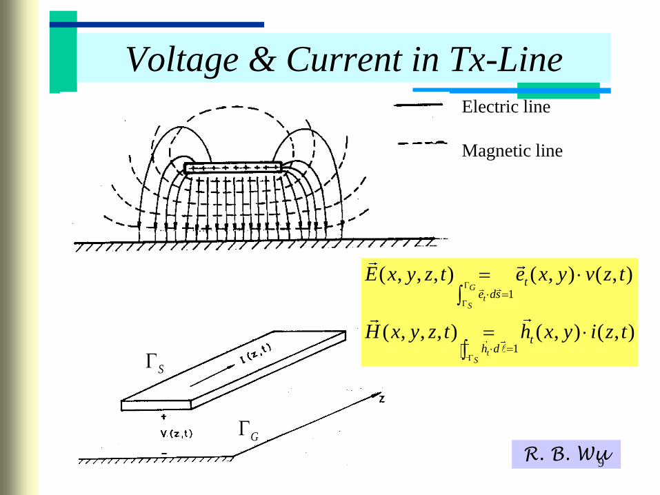
Voltage & Current in Tx-Line
1
1
( , , , ) ( , ) ( , )
( , , , ) ( , ) ( , )
G
tS
tS
te ds
th d
E x y z t e x y v z t
H x y z t h x y i z t
Electric line
Magnetic line
S
G
9

R. B. Wu
Derivation from Maxwell Equations
2
2
( , )( , ) ( , )
ABCDABCDA S
D
D
dE d B dS
dt
di z tv z z t v z t L z
dt
v iL
z t
2
2
( , )( , ) ( , )
ABCDABCDA S
D
D
dE d B dS
dt
di z tv z z t v z t L z
dt
v iL
z t
2
( , ) ( , ) ;
( , )z
d
d DS V
i z t i z z t i
d d di D dS dv C z v z t
dt dt dt
A B
CD
zSz z z
DH
t
dH d H d D dS
dt
2D
i vC
z t
Ampere’s Law
10

R. B. Wu
Derivation from Maxwell Equations
2
2
( , )( , ) ( , )
ABCDABCDA S
D
D
dE d B dS
dt
di z tv z z t v z t L z
dt
v iL
z t
2
2
( , )( , ) ( , )
ABCDABCDA S
D
D
dE d B dS
dt
di z tv z z t v z t L z
dt
v iL
z t
A B
CD
ABCDABCDA S
BE
t
dE d B dS
dt
2
( , )( , ) ( , ) D
di z tv z z t v z t L z
dt
2D
v iL
z t
Faraday’s Law
11
Suitable if simulation
2 2
1
2 D D
fL zC z

R. B. Wu
2 2, versus ,D DL C e
2ˆ
ˆ
G
S
G
S
S
D t
t
t
L h z ds
h z ds
h d
2ˆ
ˆ
S
S
G
S
D t
t
t
C e z d
z e d
e ds
e
e
ˆTEM wave t th z e
2 2D DL C e
2 2
2 22 2( , ) and ( , ) satisfy 0;D D
u uv z t i z t L C
z t
12

R. B. Wu
Solution of Wave Eq. in Phasor Form
• Wave Equation (P.D.E.)
• Wave eq. in freq. domain
2 2
2 2 2
2 2
1( , ) satisfies 0; p
p D D
v vv z t v
z v t L C
2 2
2 2
( )Phasor ( ) satisfies 0;
d V jV z V
dz c
( , ) Re ( ) j tv z t V z e
22
2
Propagation constant
0 ( ) ;
p
j z j z
v
d VV V z V e V e
dz
2 can be found since D
dVI j L I
dz
13

R. B. Wu
Wave Solution in Time Domain
20
0 2
( ; ) ( ) ( ) ; = /
1( ; ) ( ) ( ) ;
j z j z
p
j z j z D
D
V z V e V e v
LI z V e V e Z
Z C
( ) ( ); ( ) ( ) jaf t F f t a F e F F
0
( , ) ( ) ( )
1( , ) ( ) ( )
p p
p p
z zv v
z zv v
V z t V t V t
I z t V t V tZ
Solution in frequency domain
Fourier transform identity
Solution in time domain
14

Tx-Line Parameters Extraction
17

R. B. Wu
• Pure TEM does not exist
• Approximate TEM wave
– Calculation of C2D
– Calculate C0,2D: p.u.l. capacitance
with all dielectrics replaced by
free space
– Determine L2D by L2D C0,2D = 0e0
Tx-Line Parameters
D
r
DDDD
DD
D
D
rD
D
DDDD
p
cCCCcCC
CL
C
LZ
c
C
C
CLCLv
22,022,02
2,02
2
20
2
2,0
2,0222
eff
eff
1
11
e
e
D
Dr
C
C
2,0
2
effe
microstrip line
18

R. B. Wu
Determination of Line Parameters
• Analytical Tech. 1 – Conformal Mapping
– Closed-form solution of Laplace’s equation
– Applicable for several types of lines only
• Analytic Tech. 2 – Eigenfunction Expansion
• Graphical Techniques
– Very rough, but can yield intuitive feeling
• Numerical Techniques
– Calls for numerical techniques
• Empirical Formulas
– Deduce from vast measurement or simulation results
19

R. B. Wu
Analytic Techniques – by conformal mapping
)(2
ABC D
e
'ln'ln2
ABC D
e
Coaxial cable )'/'ln(
22
ABC D
e
AB eAeB ' ;'
Note: pul capacitance keeps invariant in scaling
Theory: pul capacitance keeps invariant in conformal mapping
20

R. B. Wu
Parallel Wire Capacitance
Ref: R. W. Churchill & J. W. Brown, Complex Variable & Applications,
McGraw-Hill, 1984, p.32921

R. B. Wu
Twisted Line Capacitance
1 2
2 21, 1
d dx x
r r
r
2d
1
2d/r
Scaling
22 1
2
1ln coshln 1
D
o
Cd
d dR r
r r
e e e
e e
22

R. B. Wu
Wire above Ground
122 2
lnDC
d
r
e
r
d
DC2 DC2
2
2
2;
2ln
2ln
2
D
D
Cd
r
dL
r
e
DC221
23

R. B. Wu
Analytic Tech.: Governing Eq.
• Field expression:
• Field equation:
• Stored charge:
( , , , ) ( , ) ( , ); where ( , ) satisfies:
( , ) 0
( , ) 1g
s
E x y z t e x y V z t e x y
e x y
e x y ds
ˆ ˆ( , ) ( , ) (F/m)s s
n Ed Q z t n e x y d Ce e
2
( , ) ( , )
1 on 0; ( , )
0 on
s
g
e x y x y
x y
n̂
24

R. B. Wu
Ex: Coaxial Cable
• Laplace eq.
• Sol.:
• Charge:
2
( , ) ( )
1 PDE: 0 for
BC: 1 when ; 0 when
r r
r a r br r r
r a r b
1 1 2 PDE ; ( ) ln
ln BC
ln
r C r C r Cr
b r
b a
2
0
1ˆ ˆ
ln
1 2ˆ
ln lns
e r rr r b a
C n ed ada b a b a
ee e
0
1
ab
0
1
r
r
e e e
25

R. B. Wu
Finte Difference Method
1
4 0 2
3
6
9 5 7
8
26
• Laplace eq.
• FD formula:
• Solve 122 simultaneous equations
10 1 2 3 44
( ) inside material
BC: =0 on ground
=1 on strip
2 22
2 2PDE: 0
x y
1 15 6 8 7 92(1 ) 4
( ) ( ) on material interfacer re
e
re
=0
=1
( )x y

R. B. Wu
Ex. Microstrip Line
• Assume: field can be confined with two side walls
• Laplace eq.
• Appro. Capacitance:
2 22
2 2PDE: 0 unless on metal strip
x y
BC on ground: =0
BC on metal strip:
(i) is continuous;
(ii) ( )y h
y y hxe
/2
/2
(0, )
w
y hwdxQ
CV h
27

R. B. Wu
Ex. Microstrip Line (Cont’)
• PDE + BC(ground) + BC(strip, i):
• BC(strip, ii),
• Solution by Fourier cosine series:
( )
1,3,5,...
cos sinh ; for ; , is odd
cos sinh ; for n
n n n
ny h
n n n n
A x y y h nn
A x h e y h d
Assume ( ) 1 when 2; =0 elsewherex x w
0
1,3,5,...
cos cosh sinh ( )y h
n n n r n ny y hn
A x h h xe e e
1,3,5,...
4sin 2( ) cos n
n n n
n n
wx a x a
d
0
1,3,5,...
... sinh
nn
n n n
n
a wA C
A he
?
28

R. B. Wu
Charge near Conductor Edge
• Laplace eq.
• Solution by separation of variables
• Charge distribution
22
2 2
1 1PDE: 0
BC: (i) on = & =0
rr r r r
V
1
( , ) ( ) ( );
sinn n
n n nn
r R r Y
V a r b r
2
( ) sin ;
( ') ' 0 n n
n n
n n n
Y n
r rR R R a r b r
1 1
0 1
1ˆ n n
n n nnn E E a r b r
r
e e e e
29

R. B. Wu
Charge near Conductor Edge
• Finite charge:
• Near edge (small r):
• A better charge model on microstrip
1 1
0 1on strip: n n
n n nna r b r
e
0finite 0
a
nr
Q dr b
1
13
12
11 11 1
if 3 2 (90 wedge)
if 2 (thin strip)
o
aa r r
r
r
e e
2 2
( )2
Qx
w x
Note: the singularity
is integrable30

R. B. Wu
Graphical Technique
n
j C
n
j
n
j
QQQ
V
n
mD
m
i
ij
n
ijViQmi
j
VVV
QQQ
V
QC
1
1
1
1
1
21
212
11
2
111
0
if curvilinear square
, , ij
m nC C Z
n m
ee
j
iij
V
QC
0
e.g., 26 4
0.154 377
m , n
Z
2D
QC
V
31

R. B. Wu
Parameter Estimation
• Change in orientation of electric flux line
• Effective dielectric constant
• Capacitance
9 27(1) (4) 3.25
9 27 9 27effe
0
143.25 8.85 80.5
5
p
eff
s
nC pF m
ne e
1 2
1 2
tan tan
e e
32

R. B. Wu
Numerical Tech.: Integral Eq.
0
0
Solution :
( , ) ( , ; ', ') ( ', ') '
0; 0
Integral equation:
( , ; ', ') ( ', ') ' ; ( , )
S
y r
S
x y G x y x y x y d
G x y x y x y d V x y S
2
0 r
Green's function: field at ( , ) due to point source at ( ', ')
1DE: ( , ; ', ') ( ') ( ')
BC: G 0 , G 0
t
y
x y x y
G x y x y x x y y e
2 21
In free space: ( , ; ', ') ln ' ' Const.2
G x y x y x x y ye
0
numerical method ( ', ') Q
x y Q ds CV
33

R. B. Wu
Ex: Microstrip Line
+ +
_2 2
2 2
( , ; ', ) ( , ; ', ) ( , ; ', )
( ') ( )1 ln
2 ( ') ( )
newG x y x h G x y x h G x y x h
x x y h
x x y he
( , ; ', )newG x y x h
2 2/2
/2
( ') 4( ')Integral eq.: 1 ln '
2 ' 2
w
w
x x hx wdx x
x x
e
1
Method of moments 1 for 1,2,..., ;
where ( , ; , ) ,
& analytic formula required for
N
mn n
n
mn m n
mm
G m N
G G x h x h x
G
( , ; ', )newG x y x h
34

R. B. Wu
Numerical Techniques
CAP1 CAP2 - microstrip
CAP3 – triplate
Geometry of lines:
width, separation,thickness, height,
substrate, etc.
C2D
Electrical parameters:
capacitance matrix [C]
Inductance matrix [L]
• Based on integral equation formulation
and method of moments
• Employ exact integration formulae
• Four versions are available
W. T. Weeks, “Calculation of coefficients of capacitance of multiconductor
transmission lines in the presence of a dielectric interface,” IEEE Trans.
Microwave Theory Tech., vol. 18, pp. 35-43, Jan. 1970.
CAP4 – e.g. CPW
35

R. B. Wu
CAP2 Example
36

R. B. Wu
Empirical Formula: Commercial Tool
http://web.appwave.com/Products/Microwave_Office/Feature_Guide.php?bullet_id=9 37

R. B. Wu
Simple Microstrip Formula• Parallel Plate Assumptions +
– Large ground plane with zero
thickness
• To accurately predict microstrip
impedance, you must calculate the
effective dielectric constant.
TD
TC
e
WC
From Hall, Hall & McCall:
087 5.98
ln0.81.41r
Zw te
1 1
0.217 12 122 1
r re r
tF
ww
e ee e
2
0.02 1 1 ; for 1
0 ; for 1
r w wF
w
e
Valid when:
0.1 < w < 2.0 and 1 < er < 15
You can’t beat
a field solver
C D
C D
w W T
t T T
38
Various empirical formulae are available, e.g., (3.35) & (3.36b) in textbook.

R. B. Wu
Microstrip Z0 (Rule of Thumb)
• FR4 (Er~4):
50 Ohm line in FR4 has w:h=2:1
• Al2O3氧化鋁(Er~9.9):
50 Ohm line in Al2O3 has w:h=1:1
• GaAs砷化鎵(Er~12.9):
50 Ohm line in GaAs has w:h=0.7:1
W
h
W
h
W
h
http://www.rogerscorporation.com/mwu/mwi_java/Mwij_vp.html
39

R. B. Wu
Simple Stripline Formulas
• Same assumptions as used
for microstrip apply hereTD2
TCe
WCTD1
From Hall, Hall & McCall:
)8.0(67.0
)(4ln
60 110
CC
DD
r
sym
TW
TTZ
e
Symmetric (balanced) Stripline Case TD1 = TD2
),,,2(),,,2(
),,,2(),,,2(2
00
000
rCCsymrCCsym
rCCsymrCCsymoffset
TWBZTWAZ
TWBZTWAZZ
ee
ee
Offset (unbalanced) Stripline Case TD1 > TD2
Valid when WC/(TD1+TD2) < 0.35 and TC/(TD1+TD2) < 0.25
You can’t beat a
field solver
40
Various empirical formulae are available, e.g., (3.36c) & (3.36d) in textbook.

R. B. Wu
PCB Z0 (Rule of Thumb)
• Microstrip:
50 Ohm line in FR4 has w:h=2:1
• Stripline
50 Ohm line in FR4 has w:b=1:2
• Asymmetric Stripline:
50 Ohm line in FR4 has w:h1=1.25:1, h2=2 h1
W
h
W
W
b
h2
h1
41

R. B. Wu
The “Big Four ” Tx-line Properties
There are four properties affect the performance
of most digital transmission lines:
• Impedance: reflection/distortion
• Time Delay: tx-line concern
• High-Frequency Loss: limit signal bandwidth
and transmission distance
• Crosstalk: coupling
42
Eq. Circuit Modeling
43

R. B. Wu
Transmission Line Concept
PowerPlant
ConsumerHome
Power Frequency (f) is @ 60 HzWavelength (l) is 5 106 m
( Over 3,100 Miles)
44

R. B. Wu
T Line Rules of Thumb
Td < .1 Tx
Td < .4 Tx
May treat as lumped Capacitance
Use this 10:1 ratio for accurate modeling of
transmission lines
May treat as RC on-chip, and treat as LC for PC
board interconnect
So, what are the rules of thumb to use?
45
In PCB, signal frequency (f) is approaching 10 GHz. Wavelength (l) is 1.5 cm ( 0.6 inches)

R. B. Wu
Short Lines & Tx-Lines
46

R. B. Wu
Rise Time vs. Bandwidth
%10~%90
%90~%10
fromtimefallt
fromtimeriset
f
r
r
H
H
fr
tf
ftt
35.0
35.0
fH : upper cutoff frequency
fallrise
dBt
bandwidth/
3
35.0
Max. slope
= v/T10-90
47

R. B. Wu
Myth of fH = 0.35/tr
3
1( )
1
1
2dB
Hj RC
BWRC
0
0
( ) (1 )
( ) (0.1 0.9)
( ln 0.1 ln 0.9)
2.2
t RC
r
v t V e
v t V
t RC
RC
3
2.2 0.35
2dB
r r
BWt t
Rem.: it is nothing with
the major freq. contents of
the trapezoidal pulse!
t
vi(t)
48

R. B. Wu
Spectrum of Trapezoidal Pulse
0
1
sin sin 2( ) 1 2 cos ;
,
W w r
n w r
Ww r
T
T T
T nx nx ntv t V
T nx nx T
x x
0.44 (3dB)
f0.32
0.32
WT
0.32
49

R. B. Wu
PRBS Power Spectrum
50
2.5 Gb/sec
UI = 400 ps, Tr = 50 ps
Take 28-1 periods
Similar to single pulse response
0 1 2 3 4 5 6 7 8 9 10
UI
-0.5
0
0.5
1
1.5
Vo
ltag
e (
V)
PRBS Pattern
Expect noise level to be lower if resonance occurs at the null
point of power spectrum
0 1 2 3 4 5 6 7 8 9 10 11 12 13
Freq (GHz)
-60
-50
-40
-30
-20
-10
0
No
rma
lize
d P
ow
er
Den
sit
y (
dB
)
PRBS Power Spectrum
PRBS
Pulse

R. B. Wu
Tr and BW
for Ideal Square Wave
f0.32
rt
0.32
WT
spec
trum
• It is suggested to consider significant bandwidth = 1/tr. Then,
as compared with ideal square wave, the neglected part is
even smaller by at least 20log(1/0.32) = 10dB.
• Typical example, clock freq. =1/TW, tr = 0.1TW. Then, the
neglected part is smaller than dc part by at least
20log(1/0.032)+10 = 40dB
Rise Time Bandwidth
10 nsec 100 MHz1 nsec 1 GHz100 psec 10 GHz50 psec 20 GHz
52

R. B. Wu
Did you learn
• How to derive Telegrapher eq. from Maxwell eq.?
What’s relation between v(z,t), i(z,t) and E, H?
• What is the exact solution of Telegrapher eq? How
to derive it?
• How to calculate Tx-line capacitance? Can you
solve PDE to obtain capacitance of microstrip line?
• What is the meaning of 0.35/tr? How to estimate the
major freq. content of a digital signal?
53

R. B. Wu
References & Further Reading
• W. T. Weeks, “Calculation of coefficients of capacitance of multi-conductor transmission lines in the presence of a dielectric interface,” IEEE Trans. Microwave Theory Tech., vol.18, pp. 35-43, Jan. 1970.
54