icestick evaluation kit user’s guide - lattice...
TRANSCRIPT

August 2013EB82_01.0
iCEstick Evaluation KitUser’s Guide
2
iCEstick Evaluation Kit
IntroductionThank you for choosing the Lattice Semiconductor iCEstick™ Evaluation Kit.
This guide describes how to start using the iCEstick Evaluation Kit, an easy-to-use USB form factor board for rap-idly prototyping designs using the iCE40 FPGA. Along with the evaluation board, this kit includes a pre-loaded design that demonstrates basic board functionality.
The contents of this user’s guide include demo operations, descriptions of the various portions of the evaluation board, descriptions of the on-board connectors, a complete set of schematics and bill of materials for the iCEstick Evaluation Board.
FeaturesThe iCEstick Evaluation Kit includes:
• iCEstick Evaluation Board – features the following on-board components– High-performance, low-power iCE40HX1K FPGA– FTDI 2232H USB device allows iCE device programming and UART interface to a PC– Vishay TFDU4101 IrDA transceiver– Five user LEDs– 2 x 6 position Diligent PmodTM compatible connector enables many other peripheral connections– Discera 12Mhz MEMS oscillator– Micron 32Mbit N25Q32 SPI flash– Supported by Lattice iCEcube2™ design software– USB connector provides the power supply– 16 LVCMOS/LVTTL (3.3V) digital I/O connections on 0.1” through-hole connections
• Pre-loaded demo design – the kit includes the pre-loaded demo design that flashes the on-board LEDs in a clockwise pattern.
• USB connector – provides a communication and debug port via a USB-to-RS-232 physical channel and pro-gramming interface to the PC.
Figure 1. iCEstick Evaluation Board
USBConnector
FTDI2232H
LatticeiCE40-1KHX
PrototypingHoles
IrDATransceiver
PmodConnector
SPIFlash

3
iCEstick Evaluation Kit
Figure 2. iCEstick Functional Block Diagram
USB Type A Male
Pmod
IrDA
iCE40HX1K
144TQFP
SPI
LDO
FT2232H
Pwr LED I/O LEDs
I/O Access
~4 in.
4
iCEstick Evaluation Kit
Software RequirementsBefore using the iCEstick board, download and install the latest version of Lattice iCEcube2™ and Diamond Pro-grammer. Make sure you log in to the Lattice website, otherwise these software downloads will not be visible. These are available at http://www.latticesemi.com/Products/DesignSoftwareAndIP.aspx. If you install Diamond Programmer 2.2, you will require a software patch. This software patch is available at http://www.lattice-semi.com/icestick. Go to the Downloads tab and install the appropriate patch. This patch is not required with Dia-mond Programmer 3.0 or higher.
Figure 3. Software Downloads
Download iCEcube2for HDL development
Download DiamondProgrammer for physically configuring the device
5
iCEstick Evaluation Kit
Communication Between the PC and iCEstickCommunication between the iCEstick Board and a PC is via the FTDI 2232H USB device. To enable this connec-tion the installation of the FTDI chip USB hardware drivers is needed. This driver is installed when Diamond Pro-grammer was installed. These drivers enable the computer to recognize and program the iCEstick board. In addition these drivers allow communication between the PC and the iCEstick board to enable further demonstra-tions.
Connecting the iCEstick Evaluation BoardInsert the iCEstick evaluation board to an open USB slot in a PC. The default bitstream in the SPI flash loads the iCE40HX-1k device on the iCEstick board. One should see the green LED on the board light up and continue to be lit.
Preprogrammed Design and Board LEDsThere are a total of 5 LEDs on the iCEstick board. All are controlled by I/Os of the iCE40HX-1k device. The default bitstream loads the iCE40HX-1k device and the green LED lights up signifying that the device has loaded correctly and power is good. The other four red LEDs arranged in a diamond pattern begins to flash in a clockwise direction. This is the intended function of the default bitstream.
Table 1. User I/O and LEDs
Download Demo DesignsThe above demo is pre-programmed into the iCEstick board. Other than the default design, Lattice also distributes source and programming files for demonstration designs compatible with this board. To download the demo designs:
1. Browse to www.latticesemi.com/icestick and click on the Downloads tab to view other design files and capabil-ities that the iCEstick board could implement. Various demo designs are available and can be download.
2. Extract the contents of zip files to a local hard drive.
Lattice provides the following demos based on iCEstick board:
• UART over IrDA. In this demo design, the iCEstick device communicates with a laptop or PC through UART over USB. Then, the payload is transmitted through Vishay IrDA device. This data can be locally looped back or another iCEstick board could receive the data via it’s IrDA receiver.
• Diligent Pmod Accelerometer. The demo makes use of Digilent PmodAcl module which is plugged into iCEstick board. In this demo design, the accelerometer setting and reading is done by the on-board iCE device and the direction of movement is displayed with the diamond pattern LEDs.
LED location CPLD pin (All in Bank 1) CPLD I/O LED color
D1 99 PIO1_14 Red
D2 98 PIO1_13 Red
D3 97 PIO1_12 Red
D4 96 PIO1_11 Red
D5 95 PIO1_10 Green
6
iCEstick Evaluation Kit
IrDA Functionality and DemoThe iCEstick board has a Vishay TFDU4101 IrDA transceiver on it. This device allows transmit and receive of infra-red data up to 115kbps.
Table 2. IrDA Pin Description
There are two possible configurations for the IrDA demo design: IrDA TX and IrDA RX. For an end to end complete IrDA link demo, two iCEstick boards are needed, however using just the IrDA Tx design can support a demo. The IrDA TX design transfers the data from the PC keyboard input in a terminal window to the IrDA Vishay device TXD. While the data is transmitted via infrared, it is also by default looped back to the receive channel of the IrDA device. In this demo the looped back data is received and before it is transmitted to the PC window the text is converted from lower case to upper case. This is the signal flow for the stand alone demo.
Figure 4. IrDA TX on iCEstick
Laptop or PC
iCE40
IrDA TXUART
via USB
The IrDA RX design receives infrared data from the Vishay IrDA Tx device. After the IrDA data is wirelessly received it is then sent to the iCE40 device. The iCE40 then send the character information to the open window on the PC. Thus whatever is typed in the TX terminal window is displayed in the Rx terminal window.
Figure 5. IrDA RX on iCEstick
Laptop or PC
iCE40 Vishay IrDAUART
OverUSB
This demo requires a terminal program on PC to communicate with the iCEstick board. The following instructions describe the setup for IrDA TX stand alone demo using the Tera Term terminal emulator program on Windows 7.
IrDA function CPLD pin CPLD I/O Comment
RXD 106 PIO1_19 Receive data pin
TXD 105 PIO1_18 Transmit data pin
SD 107 PIO1_20 Shut down

7
iCEstick Evaluation Kit
Setting Up for the IrDA TX Stand Alone DemoTo set up for the IrDA TX demo:
1. Program the iCE device with IrDA TX bitstream.2. Plug iCEstick into a PC USB port. 3. Check if the USB driver is installed correctly.
Go to Start, right-click Computer and select Properties. The System window is shown.Click Device Manager.
Figure 6. System Window
4. If the driver is installed correctly, the device is listed without an error tag under Ports (COM & LPT) as shown in Figure 7. Proceed to the next step.
Figure 7. Device Manager

8
iCEstick Evaluation Kit
If the driver is not installed correctly, the device is tagged with a yellow exclamation point as shown in Figure 8. You need to install the driver. To do this, right-click the device and select Update Driver Software.
Figure 8. Device Manager with Driver Error
Request Windows to search the web for the driver. After Windows locates the FTDI driver, install it and proceed to the next step.
5. Install Tera Term software. The installer can be downloaded from http://download.cnet.com/Tera-Term/3000-20432_4-75766675.html.
6. Open Tera Term. 7. In the New connection dialog box, click Serial.8. On the Port menu, click COMxx: USB Serial Port (COMxx). If there are two or more options, select the last
COM port on the list. Click OK.Figure 9. New Connection Dialog Box
9. The selected COM port/default baud rate appear in the Tera Term VT window title bar as shown in Figure 10. On the Setup menu, click Serial port.

9
iCEstick Evaluation Kit
Figure 10. Tera Term VT Window with Selected COM Port /Default Baud Rate
10. The Serial port setup dialog box opens. In the Baud rate menu, click 115200. Leave other options with default settings. Click OK.
Figure 11. Serial Port Setup Dialog Box
11. The selected COM port/115200 baud rate appear in the Tera Term VT window title bar as shown in Figure 12.
On the Setup menu, click Terminal.

10
iCEstick Evaluation Kit
Figure 12. Tera Term VT Window with Selected COM Port /Baud Rate
12. The Terminal setup dialog box opens. Select Local echo. Leave other options with default value. Click OK.
Figure 13. Terminal Setup Dialog Box
When you type in the Tera Term VT window using the TX design, a lower case character is echoed with a capital character from the iCE device as shown in the Figure 14.

11
iCEstick Evaluation Kit
Figure 14. Tera Term VT Window Using TX Design
For IrDA RX, the above Tera Term setting is the same but the bitstream for the iCE device is different. With a setup of two iCEstick boards facing each other, one programmed with IrDA TX and the other programmed with IrDA RX, the character typed in IrDA TX PC is transferred to and displayed on IrDA RX PC monitor. You can change the angle of the TX board facing the RX board to see when the IrDA link would break.

12
iCEstick Evaluation Kit
Diligent Pmod Connector and Accelerometer DemoOn the iCEstick board, location J2 is a 2x6 position Pmod (Peripheral MODule) Digilent connector. The iCEstick board supports a variety of Pmod peripheral modules for easy I/O expansion. Figure 3 lists the 0.1” through-hole headers on the iCEstick board that support Pmod modules. Pmod modules come in different form factors, and each Pmod header includes power and ground supplies. The easiest way to support a Pmod module is to add the appropriate female socket. Straight-through or right-angle connectors can be used. Male headers are an alternate solution when using the interface cable provided with most Pmod modules.
Table 3. Diligent Pmod Compatible Connector Description
The Accelerometer demo makes use of the Digilent PmodAcl accelerometer module from Diligent. The PmodAcl module needs to be plugged into J2 on the iCEstick board through the cable that comes with this module. The four LEDs D1, D2, D3 and D4 in the north, south, east and west pattern are configured to represent X+, Z+, X-, Z- of accelerometer movement direction respectively. When the accelerometer module is moved around, the diamond pattern LEDs on the iCEstick board goes on/off corresponding to the direction of the movement and orientation of the module. If all these LEDs light up at the same time (indicating a balance point), The D5 LED also lights up.
Figure 15. Accelerometer Demo on iCEstick
Accelerometer Demo on iCEstick
iCE40 LEDAcl Module
Connection Left Row pins Right Row pins Connection
PIO1_02 1 7 PIO1_06
PIO1_03 2 8 PIO1_07
PIO1_04 3 9 PIO1_08
PIO1_05 4 10 PIO1_09
Ground 5 11 Ground
3.3v 6 12 3.3v

Programming Demo Designs with Lattice ProgrammerTo program a bitstream file to iCE device:
1. Plug the iCEstick board to a USB port on a host PC with Programmer installed.2. Run Programmer. The Diamond Programmer Getting Started window opens. Under Select an Action, click
Create a new Blank Project. Click OK. If you try to create a new project from a scan, you will receive an error. Please select Create a new Blank Project.
Figure 16. Diamond Programmer Getting Started Window
3. The Diamond Programmer interface opens. Under Cable Settings, in the Cable menu, click USB2. In the Port menu, click FTUSB-0. You can also click Detect Cable to set the correct cable and port.
Figure 17. Cable and Port Settings
4. Select the Enable check box.5. Double-click the cell under Device Family and click iCE40.

Figure 18. Device Family Options
6. Double-click the cell under Device and click iCE40HX1K.Figure 19. Device Options
7. Double-click the cell under Operation. The Device Properties dialog box opens as shown in Figure 20. On the Access Mode menu, click SPI Flash Programming. Click OK.Warning: NVCM Programming is NOT recommended. NVCM Programming is one time programming. If you use NVCM Programming to program iCE device, the iCE device can no longer be reprogrammed.

Figure 20. Device Properties Dialog Box
8. Select the SPI flash part number. For the iCEstick, this is Micron SPI-N25Q032 8-pin VDFPN8 package. Also make sure to select the programming file. Once done, click OK.
Figure 21. Select Serial SPI Flash
9. On the Programmer toolbar, click the Program button to initiate the download. The bitstream starts download-ing to the iCE device. This takes a few seconds to complete.

Expansion I/O ConnectionsThe iCEstick board contains two unpopulated 0.1” headers for users to implement their own connections. Connec-tors J1 and J3 each consist of 10 positions for a total of 20 connections. Two of these are tied to 3.3v and two are tied to ground. This leaves 16 general purpose I/Os that connect to the iCE40HX-1k device for user I/O.
Table 4. Expansion I/O Connections
Test PointsThere are three unpopulated test points. TP1 is tied to 3.3v, TP2 is tied to 1.2v and TP3 is connected to ground.
Lattice Demonstration Bitstreams All demonstration bitstreams and Design files are available at www.latticesemi.com/icestick.
Technical Support Assistancee-mail: [email protected]
Internet: www.latticesemi.com
Revision HistoryDate Version Change Summary
August 2013 01.0 Initial release.
© 2013 Lattice Semiconductor Corp. All Lattice trademarks, registered trademarks, patents, and disclaimers are as listed at www.latticesemi.com/legal. All other brand or product names are trademarks or registered trademarks of their respective holders. The specifications and information herein are subject to change without notice.
J1 Connector J3 Connector
Pin CPLD I/O Bank 0 CPLD Pin Pin CPLD I/O Bank 2 CPLD Pin
1 3.3v - 1 3.3v -
2 Ground - 2 Ground -
3 PIO0_02 112 3 PIO2_17 62
4 PIO0_03 113 4 PIO2_16 61
5 PIO0_04 114 5 PIO2_15 60
6 PIO0_05 115 6 PIO2_14 56
7 PIO0_06 116 7 PIO2_13 48
8 PIO0_07 117 8 PIO2_12 47
9 PIO0_08 118 9 PIO2_11 45
10 PIO0_09 119 10 PIO2_10 44

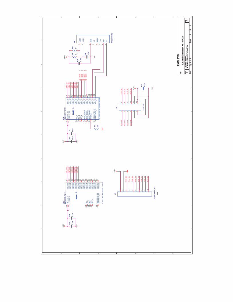
Appendix A. Schematic Diagrams
5 5
4 4
3 3
2 2
1 1
DD
CC
BB
AA
FPGA
Power from USB 5V
BANK 3
BANK 1
BANK 0
BANK 2
iCE40-HX1K-TQ144
HEADER HEADER
HEADER
I/Os
I/Os
I/Os
HEADER
I/Os
RS232
USB
CONNECTOR
USB to
SPI / RS232
LEDS
SPI
Title
veR
rebmu
N tnemuco
DeziS
teehS:eta
Dof
AXE
LSYS
ICE
40H
X1K
-STI
CK
-EV
NA
iCE
stic
k E
valu
atio
n K
it - B
lock
Dia
gram
B
15
Apr 1
2, 2
013
Title
veR
rebmu
N tnemuco
DeziS
teehS:eta
Dof
AXE
LSYS
ICE
40H
X1K
-STI
CK
-EV
NA
iCE
stic
k E
valu
atio
n K
it - B
lock
Dia
gram
B
15
Apr 1
2, 2
013
Title
veR
rebmu
N tnemuco
DeziS
teehS:eta
Dof
AXE
LSYS
ICE
40H
X1K
-STI
CK
-EV
NA
iCE
stic
k E
valu
atio
n K
it - B
lock
Dia
gram
B
15
Apr 1
2, 2
013

5 5
4 4
3 3
2 2
1 1
DD
CC
BB
AA
SCK
SI SO
FT_E
ECS
FT_E
ECLK
FT_E
EDAT
A
SS
+3.3
V
VCC
1_8F
T
VCC
1_8F
T
+3.3
V
+3.3
V+3
.3V
+3.3
V
+3.3
V
+3.3
V
+3.3
V
iCE_
SCK
4iC
E_M
OSI
4iC
E_M
ISO
4
iCE_
SS_B
4
DM
5D
P5
RS2
32_R
x_TT
L4
RS2
32_T
x_TT
L4
RTS
n4
DTR
n4
CTS
n4
DSR
n4
DC
Dn
4
iCE_
CLK
4
iCE_
CD
ON
E4
iCE_
CR
EST
4
Title
veR
rebmu
N tnemuco
DeziS
teehS:eta
Dof
AXE
LSYS
ICE
40H
X1K
-STI
CK
-EV
NA
iCE
stic
k E
valu
atio
n K
it - U
SB
to S
PI/R
S23
2
B
25
Apr 1
2, 2
013
Title
veR
rebmu
N tnemuco
DeziS
teehS:eta
Dof
AXE
LSYS
ICE
40H
X1K
-STI
CK
-EV
NA
iCE
stic
k E
valu
atio
n K
it - U
SB
to S
PI/R
S23
2
B
25
Apr 1
2, 2
013
Title
veR
rebmu
N tnemuco
DeziS
teehS:eta
Dof
AXE
LSYS
ICE
40H
X1K
-STI
CK
-EV
NA
iCE
stic
k E
valu
atio
n K
it - U
SB
to S
PI/R
S23
2
B
25
Apr 1
2, 2
013
R44
0R
440
C13
0.1u
F
C13
0.1u
F
C4
0.1u
F
C4
0.1u
F
R4
0R
40
C12
0.1u
F
C12
0.1u
F
R6
12K
R6
12K
R9
10K
R9
10K
C7
0.1u
F
C7
0.1u
F
X1
12.0
000M
HZ
X1
12.0
000M
HZVD
D4
STAN
DBY
#1
GN
D2
OU
TPU
T3
R7
10K
R7
10K
R12
0R
120
R10
0R
100
R17
0R
170
R3
0R
30
C11
0.1u
F
C11
0.1u
F
R14
0R
140
R15
2.2K
R15
2.2K
R18
0R18
0
R5
2.2K
R5
2.2K
C6
0.1u
F
C6
0.1u
F
C3
4.7u
F
C3
4.7u
F
C9
0.1u
F
C9
0.1u
F
R2
0R
20
C2
0.1u
F
C2
0.1u
F
R8
10K
R8
10K
C10
10uF
C10
10uF
R13
0R
130
C8
0.1u
F
C8
0.1u
F
FTDI
Hig
h-Sp
eed
USB
F
T223
2H
FT22
32H
LU
1
FTDI
Hig
h-Sp
eed
USB
F
T223
2H
FT22
32H
LU
1
VREG
IN50
VREG
OU
T49
DM
7
DP
8
REF
6
RES
ET#
14
EEC
S63
EEC
LK62
EED
ATA
61
OSC
I2
OSC
O3
TEST
13
ADBU
S016
ADBU
S117
ADBU
S218
ADBU
S319
VPHY4
VPLL9
VCORE12
VCORE37
VCORE64
VCCIO20
VCCIO31
VCCIO42
VCCIO56
AGND10
GND1
GND5
GND11
GND15
GND25
GND35
GND47
GND51PW
REN
#60
SUSP
END
#36
ADBU
S421
ADBU
S522
ADBU
S623
ADBU
S724
ACBU
S026
ACBU
S127
ACBU
S228
ACBU
S329
ACBU
S430
ACBU
S532
ACBU
S633
ACBU
S734
BDBU
S038
BDBU
S139
BDBU
S240
BDBU
S341
BDBU
S443
BDBU
S544
BDBU
S645
BDBU
S746
BCBU
S048
BCBU
S152
BCBU
S253
BCBU
S354
BCBU
S455
BCBU
S557
BCBU
S658
BCBU
S759
R11
0R
110
R45
0R
450
R16
0R
160
R1
0R
10
C5
0.1u
F
C5
0.1u
F
C1
4.7u
F
C1
4.7u
F
93LC
56-S
O8
U2
93LC
56-S
O8
U2
CS
1
CLK
2
DI
3
DO
4VS
S5
OR
G6
NU
7VC
C8
5 5
4 4
3 3
2 2
1 1
DD
CC
BB
AA
PIO
1_02
PIO
1_03
PIO
1_04
PIO
1_05
PIO
1_06
PIO
1_07
PIO
1_08
PIO
1_09
PIO
1_02
PIO
1_03
PIO
1_04
PIO
1_05
PIO
1_06
PIO
1_07
PIO
1_08
PIO
1_09
PIO
0_02
PIO
0_03
PIO
0_04
PIO
0_05
PIO
0_06
PIO
0_07
PIO
0_08
PIO
0_09
PIO
0_02
PIO
0_03
PIO
0_04
PIO
0_05
PIO
0_06
PIO
0_07
PIO
0_08
PIO
0_09
+3.3
V
+3.3
V+3
.3V
+3.3
V
+3.3
V
LED
45
LED
35
LED
25
LED
15
LED
05
Title
veR
rebmu
N tnemuco
DeziS
teehS:eta
Dof
AXE
LSYS
ICE
40H
X1K
-STI
CK
-EV
NA
iCE
stic
k E
valu
atio
n K
it - F
PG
A
B
35
Apr 1
2, 2
013
Title
veR
rebmu
N tnemuco
DeziS
teehS:eta
Dof
AXE
LSYS
ICE
40H
X1K
-STI
CK
-EV
NA
iCE
stic
k E
valu
atio
n K
it - F
PG
A
B
35
Apr 1
2, 2
013
Title
veR
rebmu
N tnemuco
DeziS
teehS:eta
Dof
AXE
LSYS
ICE
40H
X1K
-STI
CK
-EV
NA
iCE
stic
k E
valu
atio
n K
it - F
PG
A
B
35
Apr 1
2, 2
013
R19
47R19
47
J1
Fem
ale
head
er 1
x10
DN
I
J1
Fem
ale
head
er 1
x10
DN
I
82 4 6 7531 109
C16
0.1u
F
C16
0.1u
F
C19
4.7u
F
C19
4.7u
F
C17
0.1u
F
C17
0.1u
F
R21
10K
R21
10K
C15
0.1u
F
C15
0.1u
F
BANK 0
NC p
ins
may
be r
oute
d th
roug
h
iCE4
0HX1
K-TQ
144
U3A
BANK 0
NC p
ins
may
be r
oute
d th
roug
h
iCE4
0HX1
K-TQ
144
U3A G
BIN
0/PI
O0_
0012
9
GBI
N1/
PIO
0_01
128
NC
_111
0
NC
_212
4
NC
_312
5
NC
_413
0
VCC
IO0_
0113
3
VCC
IO0_
0212
3
NC
_19
131
PIO
0_02
112
PIO
0_03
113
PIO
0_04
114
PIO
0_05
115
PIO
0_06
116
PIO
0_07
117
PIO
0_08
118
PIO
0_09
119
PIO
0_10
120
PIO
0_11
121
PIO
0_12
122
PIO
0_13
134
PIO
0_14
135
PIO
0_15
136
PIO
0_16
137
PIO
0_17
138
PIO
0_18
139
PIO
0_19
141
PIO
0_20
142
PIO
0_21
143
PIO
0_22
144
R20
47R20
47U
4
TFD
U41
01-T
R3
U4
TFD
U41
01-T
R3
GN
D8
IRED
C2
RXD
4TX
D3
SD5
VCC
16
NC
7
VCC
21
NC p
ins
may
be r
oute
d th
roug
h
BANK 1
iCE4
0HX1
K-TQ
144
U3B
NC p
ins
may
be r
oute
d th
roug
h
BANK 1
iCE4
0HX1
K-TQ
144
U3B G
BIN
2/PI
O1_
0094
GBI
N3/
PIO
1_01
93
NC
_582
NC
_683
NC
_784
NC
_885
PIO
1_21
/TC
K75
PIO
1_22
/TD
I73
PIO
1_23
/TD
O76
PIO
1_24
/TM
S74
TRST
_B77
VCC
IO1_
0189
VCC
IO1_
0210
0PI
O1_
0278
PIO
1_03
79
PIO
1_04
80
PIO
1_05
81
PIO
1_06
87
PIO
1_07
88
PIO
1_08
90
PIO
1_09
91
PIO
1_10
95
PIO
1_11
96
PIO
1_12
97
PIO
1_13
98
PIO
1_14
99
PIO
1_15
101
PIO
1_16
102
PIO
1_17
104
PIO
1_18
105
PIO
1_19
106
PIO
1_20
107
J2J2
Pmod
2x6
82 4 6
7
531
109 1211
C20
0.1u
F
C20
0.1u
F
C18
0.1u
F
C18
0.1u
F
C14
0.1u
F
C14
0.1u
F

5 5
4 4
3 3
2 2
1 1
DD
CC
BB
AA
PIO
2_17
PIO
2_16
PIO
2_15
PIO
2_14
PIO
2_13
PIO
2_12
PIO
2_11
PIO
2_10
PIO
2_10
PIO
2_11
PIO
2_12
PIO
2_13
PIO
2_14
PIO
2_15
PIO
2_16
PIO
2_17
+3.3
V
+3.3
V
+3.3
V
+3.3
V
+3.3
V
iCE_
CLK
2
RS2
32_T
x_TT
L2
RS2
32_R
x_TT
L2
DSR
n2
RTS
n2
DTR
n2
DC
Dn
2
iCE_
MO
SI2
iCE_
SCK
2
iCE_
SS_B
2
CTS
n2
iCE_
MIS
O2
iCE_
CD
ON
E2
iCE_
CR
EST
2
Title
veR
rebmu
N tnemuco
DeziS
teehS:eta
Dof
AXE
LSYS
ICE
40H
X1K
-STI
CK
-EV
NA
iCE
stic
k E
valu
atio
n K
it - F
PG
A
B
45
Apr 1
6, 2
013
Title
veR
rebmu
N tnemuco
DeziS
teehS:eta
Dof
AXE
LSYS
ICE
40H
X1K
-STI
CK
-EV
NA
iCE
stic
k E
valu
atio
n K
it - F
PG
A
B
45
Apr 1
6, 2
013
Title
veR
rebmu
N tnemuco
DeziS
teehS:eta
Dof
AXE
LSYS
ICE
40H
X1K
-STI
CK
-EV
NA
iCE
stic
k E
valu
atio
n K
it - F
PG
A
B
45
Apr 1
6, 2
013
C24
0.1u
F
C24
0.1u
F
C23
0.1u
F
C23
0.1u
F
C26
0.1u
F
C26
0.1u
F
NC p
ins
may
be r
oute
d th
roug
h
BANK 3
iCE4
0HX1
K-TQ
144
U3D
NC p
ins
may
be r
oute
d th
roug
h
BANK 3
iCE4
0HX1
K-TQ
144
U3D G
BIN
6/PI
O3_
00/D
P08A
21
GBI
N7/
PIO
3_01
/DP0
7B20
NC
_10
15
NC
_11
16
NC
_12
17
NC
_13
18
VCC
IO3_
016
VCC
IO3_
0230
PIO
3_02
/DP0
0A1
PIO
3_03
/DP0
0B2
PIO
3_04
/DP0
1A3
PIO
3_05
/DP0
1B4
PIO
3_06
/DP0
2A7
PIO
3_07
/DP0
2B8
PIO
3_08
/DP0
3A9
PIO
3_09
/DP0
3B10
PIO
3_10
/DP0
4A11
PIO
3_11
/DP0
4B12
PIO
3_12
/DP0
7A19
PIO
3_13
/DP0
8B22
PIO
3_14
/DP0
9A23
PIO
3_15
/DP0
9B24
PIO
3_16
/DP1
0A25
PIO
3_17
/DP1
0B26
PIO
3_18
/DP1
1A28
PIO
3_19
/DP1
1B29
PIO
3_20
/DP1
2A31
PIO
3_21
/DP1
2B32
PIO
3_22
/DP1
3A33
PIO
3_23
/DP1
3B34
C22
0.1u
F
C22
0.1u
F
J3
Fem
ale
head
er 1
x10
DN
I
J3
Fem
ale
head
er 1
x10
DN
I
82 4 6 7531 109
R46
10K
R46
10K
R27
10K
R27
10K
C25
0.1u
F
C25
0.1u
F
C21
0.1u
F
C21
0.1u
F
R22
10K
R22
10K
BANK 2
NC p
ins
may
be r
oute
d th
roug
h
iCE4
0HX1
K-TQ
144
U3C
BANK 2
NC p
ins
may
be r
oute
d th
roug
h
iCE4
0HX1
K-TQ
144
U3C C
DO
NE
65
CR
ESET
_B66
GBI
N5/
PIO
2_01
49G
BIN
4/PI
O2_
0250
NC
_955
PIO
2_18
/CBS
EL0
63
PIO
2_19
/CBS
EL1
64
VCC
IO2_
0146
VCC
IO2_
0257
PIO
2_00
52
PIO
2_03
58
PIO
2_04
37
PIO
2_05
38
PIO
2_06
39
PIO
2_07
41
PIO
2_08
42
PIO
2_09
43
PIO
2_10
44
PIO
2_11
45
PIO
2_12
47
PIO
2_13
48
PIO
2_14
56
PIO
2_15
60
PIO
2_16
61
PIO
2_17
62
R23
0 DN
I
R23
0 DN
I
SPI
iCE4
0HX1
K-TQ
144
U3E SPI
iCE4
0HX1
K-TQ
144
U3E SP
I_VC
C72
PIO
S_00
/SPI
_SC
K70
PIO
S_01
/SPI
_SI
68
PIO
S_02
/SPI
_SO
67
PIO
S_03
/SPI
_SS_
B71
R26
10K
R26
10K
U5
N25
Q03
2A13
ESC
40F
U5
N25
Q03
2A13
ESC
40F
CS
1
SDI
5
SCK
6
WP
3
HO
LD7
VCC8
GND4
SDO
2
R24
10K
R24
10K
R25
10K
R25
10K

5 5
4 4
3 3
2 2
1 1
DD
CC
BB
AA
LEDs
+3.3
V
VBU
S_5V
+1.2
V
+3.3
V+1
.2V
+1.2
V
+3.3
V
+1.2
V
VBU
S_5V
+3.3
V+3
.31V
+1.2
2V+1
.2V
DM
2D
P2
LED
03
LED
13
LED
23
LED
33
LED
43
Title
veR
rebmu
N tnemuco
DeziS
teehS:eta
Dof
AXE
LSYS
ICE
40H
X1K
-STI
CK
-EV
NA
iCE
stic
k E
valu
atio
n K
it - P
ower
, LE
Ds
B
55
Apr 1
2, 2
013
Title
veR
rebmu
N tnemuco
DeziS
teehS:eta
Dof
AXE
LSYS
ICE
40H
X1K
-STI
CK
-EV
NA
iCE
stic
k E
valu
atio
n K
it - P
ower
, LE
Ds
B
55
Apr 1
2, 2
013
Title
veR
rebmu
N tnemuco
DeziS
teehS:eta
Dof
AXE
LSYS
ICE
40H
X1K
-STI
CK
-EV
NA
iCE
stic
k E
valu
atio
n K
it - P
ower
, LE
Ds
B
55
Apr 1
2, 2
013
C44
10uF
C44
10uF
D4
Red
D4
Red
1 2
TP2
DN
I
TP2
DN
I 1
R37
1KR37
1K
C40
0.01
uF
C40
0.01
uF
C35
1uF
C35
1uF
C43
0.1u
F
C43
0.1u
F
R41
1KR41
1K
R35
100
R35
100
R38
1KR38
1K
R34
0.1
R34
0.1
U6
LT30
30EF
E#TR
PBF
U6
LT30
30EF
E#TR
PBF
GND35
IN1_
118
SHD
N2
11
GND215
PWR
GD
119
IN1_
217
IN2_
114
PWR
GD
212
GND46
IN2_
213
SHD
N1
20
GND116
OU
T1_1
3
OU
T1_2
4
BYP1
2
ADJ1
1
OU
T2_1
7
OU
T2_2
8
BYP2
9
ADJ2
10TH
ERM
PAD
21
R43
100
R43
100
C34
10uF
C34
10uF
C33
0.01
uF
C33
0.01
uF
D3
Red
D3
Red
1 2
C41
4.7u
F
C41
4.7u
F
R32
1MR32
1M
C31
0.1u
F
C31
0.1u
F
C29
0.1u
F
C29
0.1u
F
TP3
DN
I
TP3
DN
I 1
D5
Gre
enD
5G
reen
1 2TP1
DN
I
TP1
DN
I 1
D2
Red
D2
Red
1 2
C39
10uF
C39
10uF
POWER
iCE4
0HX1
K-TQ
144
U3F POWER
iCE4
0HX1
K-TQ
144
U3F G
ND
_01
5
GN
D_0
213
GN
D_0
314
GN
D_0
459
GN
D_0
569
GN
D_0
686
GN
D_0
710
3
GN
D_0
813
2
GN
D_0
914
0
PLLG
ND
35PL
LVC
C36
NC
_14
127
NC
_15
53N
C_1
612
6N
C_1
754
NC
_18
40
VCC
_01
51
VCC
_02
27
VCC
_03
92
VCC
_04
111
VPP_
2V5
108
VPP_
FAST
109
C42
0.01
uF
C42
0.01
uF
R33
210K
R33
210K
R40
1KR40
1K
C28
1uF
C28
1uF
R39
1KR39
1K
R30
100
R30
100
C27
10uF
C27
10uF
D1
Red
D1
Red
1 2
C38
10uF
C38
10uF
C37
0.01
uF
C37
0.01
uF
R31
1MR31
1M
C36
0.1u
F
C36
0.1u
F
C32
0.1u
F
C32
0.1u
F
J4
USB
AM
90
J4
USB
AM
90
VCC
1
D-
2
D+
3
GN
D4
R29
357K
R29
357K
R28
0.1
R28
0.1
C30
0.1u
F
C30
0.1u
F
C45
0.1u
F
C45
0.1u
F
D6
CD
BU05
20
D6
CD
BU05
20
12