ic-ht dual cw laser diode driver · pdf filedual cw laser diode driver ic-ht can operate two...
TRANSCRIPT
preliminary
preliminary iC-HTDUAL CW LASER DIODE DRIVER
Rev B1, Page 1/45
FEATURES
♦ Dual channel CW operation with up to 750 mA per channel
♦ Up to 1500 mA with both channels combined
♦ 2.8 V to 11 V power supply
♦ Operation with or without µController
♦ Individual enable input per channel
♦ Control loop accuracy better than 1%
♦ Internal programmable logarithmic monitor resistor
♦ Operating point setup with 10 bit logarithmic resolution
♦ ACC or APC mode individually configurable for each channel
♦ A/D converters for analog monitoring
♦ Serial programming interface (SPI or I2C compliant)
♦ Configuration content verification and validation
♦ Programmable laser overcurrent protection
♦ Optimized for N-type laser diodes
♦ Low drop linear regulator for 3.3 V
♦ Low current standby mode
♦ Temperature monitor
♦ Temperature range -40 . . . 85 °C
APPLICATIONS
♦ Laser diode and LED modules
♦ CW N-/M-type laser diode
drivers
♦ Embedded laser diode
controllers
♦ Structured-light 3D illuminations
♦ Multiple laser diode control
♦ Optical amplification/pumping
♦ Safety related laser controllers
PACKAGES
QFN28 5 mm x 5 mm
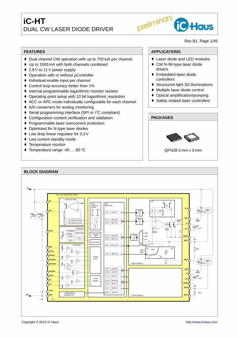
BLOCK DIAGRAM
CHECK
VB UNDERVOLTAGE
VDD UNDERVOLTAGE
RAM
PODO
RM2MONITOR 8 Bit
A
8 Bit
0x18 REF2(9:8)
0x17 RMD2(7:0)
INTEGRITY
1μF
0x14
CFGTIMOWATCHDOG WATCHDOG
TIMER
OSCILLATOR
LASER
CONTROL
0x13 REF1(9:8)
RMD1(7:0)
D
REGISTERS
SPI/I2C 2550
RM1
0x03 ADC1(9:8)
..10 nF..
0x10
10 Bit
D
8 Bit
A
IO DRIVERS
A
10 Bit
ACC
SLAVE
RAM
ILIM2(7:0)
0x11 ILIM1(7:0)
0x05 ADC2(9:8)
0x06 ADC2(7:0)
LASER CHANNEL 1
DOVC
MEMERR
0x19 REF2(7:0)
APC
REF1(7:0)
OVT 0x04 ADC1(7:0)
0x10
0x1F
0x30
0x3F
0x16
LASER CHANNEL 2
VDD REGULATOR
TEMPERATURE
..10 nF..
R
0x02
0x12
1μF
ADCC1(2:0)
DUAL CW LASER DIODE DRIVER
I LDK1
TEMP(7:0)
=1
+
-
N
+
-
I LDK2
N
CI1
CI2
CVB CVDD
LDK1
EMC
T.PAD
GND
VDD
VBREF
ADSNF1
EACC1
OVC1
DISP1
EMC
MDA1
LDK1
CIL1
AGND1
VB
LDK2
CI2
AGND2
MDA2
CIL2
MRL2
MRL1
CI1CI
ECIE1
DCO
GND
Check
NCHK
EC1
NSTBY
INS/WKR
MISO/SDA
SCLK/SCL
MOSI/A0
NCS/A1
EC2
VDD
VB
=1
I LDK1
I LDK2
N
CI1
NCVB CVDD
CI2
Copyright © 2015 iC-Haus http://www.ichaus.com

preliminary
preliminary iC-HTDUAL CW LASER DIODE DRIVER
Rev B1, Page 2/45
DESCRIPTION
Dual CW laser diode driver iC-HT can operate two in-
dividual laser diodes with up to 750 mA laser current
depending on the heat dissipation. Each channel can
be enabled independently. The laser diode driver can
be controlled by an external microcontroller (MCU
mode) or operate stand alone with pin/resistor config-
uration (iC-WK mode). In MCU mode, both channels
can be combined for driving up to 1500 mA.
Each channel can be operated individually either in
automatic current control (ACC) or automatic power
control (APC). All parameters including the internal
reference voltages are set via serial communication
(I2C or SPI). A 10 bit resolution D/A converter with
logarithmic characteristic is used for setting the oper-
ating point. This allows an operating point resolution
better than 1%.
In APC control, the monitor diode photocurrent is
used to track the optically emitted power of the laser
diode. The feedback for the laser diode driver is the
voltage of the photocurrent at a monitor resistor. An 8
bit internal programmable logarithmic monitor resis-
tor (PLR) or an external monitor resistor can be se-
lected for closing the control loop. The PLR ranges
from 100Ω to 500 kΩ with a step width less than 5%.
In ACC control, the laser diode current can be set
directly. Two current ranges are selectable.
iC-HT allows disabling the laser channels when an
overcurrent threshold has been exceeded. The over-
current threshold of each channel has 2 ranges and
is programmable through an 8 bit linear D/A con-
verter.
The temperature monitor measures the internal chip
temperature. iC-HT disables the laser channels
when overtemperature is detected.
A variety of voltages can be measured with a 10 bit
A/D converter. The following voltages can be mea-
sured:
• V(LDKx)
• V(VDD)
• V(VB)
• V(MDAx)
• V(PLRx)
The DCO current output pin can control an external
DC/DC converter. Controlling the DC/DC output volt-
age can optimize the power dissipation of the whole
system e.g. to extend battery life.
iC-HT in standby mode has a very low current con-
sumption (< 10 µA) and does retain its configuration.
The device features for safe operation:
• Configuration verification
• Tri-state configuration pins
• Write protection in operating mode
• Safe default/startup state

preliminary
preliminary iC-HTDUAL CW LASER DIODE DRIVER
Rev B1, Page 3/45
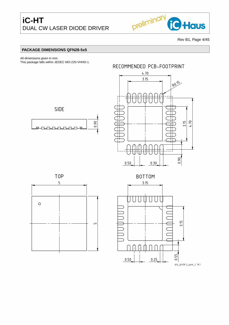
PACKAGING INFORMATION QFN28 5 mm x 5 mm to JEDEC
PIN CONFIGURATION QFN28 5 mm x 5 mm
(topview)
1
2
3
4
5
6
7
8 9 10 11 12 13 14
15
16
17
18
19
20
21
22232425262728
PIN FUNCTIONS
No. Name Function
1 LDK1 Laser Diode Cathode for channel 1
2 LDK1 Laser Diode Cathode for channel 1
3 AGND1 Analog Ground for channel 1
4 CI1 Integration Capacitor for channel 1
5 CIL1 Integration Capacitor for channel 1,
low side
6 MDA1 Monitor Diode Anode for channel 1
7 MRL1 Monitor Resistor for channel 1, low
side
8 EMC Enable Microcontroller input
9 SCLK/SCL SPI Clock / I2C Clock
10 MISO/SDA SPI Master In Slave OUT / I2C Data
11 MOSI/A0 SPI Master Out Slave In / I2C Ad-
dress Bit 0
12 NCS/A1 Chip Select, active low / I2C Ad-
dress bit 1
13 EC1 Enable Channel 1 input
14 EC2 Enable Channel 2 input
15 MRL2 Monitor Resistor for channel 2, low
side
16 MDA2 Monitor Diode Anode for channel 2
17 CIL2 Integration Capacitor for channel 2,
low side
18 CI2 Integration Capacitor for channel 2
19 AGND2 Analog Ground for channel 2
20 LDK2 Laser Diode Cathode for channel 2
21 LDK2 Laser Diode Cathode for channel 2
22 GND Ground
23 DCO Digital Current Output
24 INS/WKR I2C or SPI selection input / Refer-
ence voltage selection in iC-WK
mode
25 VDD 3.3 V output supply
26 VB Power supply
27 NCHK Error output, active low
28 NSTBY Standby input, active low
TP Thermal Pad (GND)
The Thermal Pad is to be connected to a Ground Plane (GND, AGND1. . . 2) on the PCB.
Only pin 1 marking on top or bottom defines the package orientation ( HT label and coding is subject
to change).
preliminary
preliminary iC-HTDUAL CW LASER DIODE DRIVER
Rev B1, Page 4/45
PACKAGE DIMENSIONS QFN28-5x5
All dimensions given in mm.
This package falls within JEDEC MO-220-VHHD-1.
5
5
TOP
0.250.50
3.153.15
0.55
BOTTOM
0.90
SIDE
4.70
3.15
4.70
0.50
R0.15
3.15
0.90
0.30
RECOMMENDED PCB-FOOTPRINT
drb_qfn28-2_pack_1, 10:1

preliminary
preliminary iC-HTDUAL CW LASER DIODE DRIVER
Rev B1, Page 5/45
ABSOLUTE MAXIMUM RATINGS
These ratings do not imply permissible operating conditions; functional operation is not guaranteed. Exceeding these ratings may damage
the device.
Item Symbol Parameter Conditions UnitNo. Min. Max.
G001 VB Voltage at VB -0.3 11 V
G002 I(VB) Current in VB -20 50 mA
G003 VDD Voltage at VDD -0.3 5.5 V
G004 I(VDD) Current in VDD -20 1 mA
G005 V() Voltage at CI1, CI2, EC1, EC2, MDA1,
MDA2, EMC, SCLK/SCL, MISO/SDA,
MOSI/A0, NCS/A1, DCO, INS/WKR,
NCHK
-0.3 5.5 V
G006 I() Current in CI1, CI2, EC1, EC2, MDA1,
MDA2, EMC, SCLK/SCL, MISO/SDA,
MOSI/A0, NCS/A1, DCO, INS/WKR,
NCHK, NSTBY, CIL1, CIL2, MRL1,
MRL2
-20 20 mA
G007 I(LDK) Current in LDK1, LDK2 DC current -20 900 mA
G008 V() Voltage at LDK1, LDK2, NSTBY -0.3 11 V
G009 V() Voltage at AGND1, AGND2 -0.3 1 V
G010 I(AGND) Current in AGND1, AGND2 DC current -900 1 mA
G011 Vd() ESD Susceptibility at all pins HBM 100 pF discharged through 1.5 kΩ 2 kV
G012 Tj Operating Junction Temperature -40 125 °C
G013 Ts Storage Temperature Range -40 150 °C
THERMAL DATA
Operating Conditions: VB = 2.8 . . . 11 V (referenced to GND)
Item Symbol Parameter Conditions UnitNo. Min. Typ. Max.
T01 Ta Operating Ambient Temperature Range -40 85 °C
T02 Rthja Thermal Resistance Chip/Ambient Mounted on PCB 25 K/W
T03 RthjTP Thermal Resistance Chip/Thermal Pad 4 K/W
All voltages are referenced to ground unless otherwise stated.
All currents flowing into the device pins are positive; all currents flowing out of the device pins are negative.
preliminary
preliminary iC-HTDUAL CW LASER DIODE DRIVER
Rev B1, Page 6/45
ELECTRICAL CHARACTERISTICS
Operating Conditions: VB = 2.8 . . . 11 V (referenced to GND), Tj = -40 . . . 125 °C unless otherwise stated
Item Symbol Parameter Conditions UnitNo. Min. Typ. Max.
Total Device
Functionality and parameters beyond the operating conditions (with reference to independent voltage supplies, for instance) are to be
verified within the individual application using FMEA methods.
001 VB Permissible Supply Voltage Referenced to GND 2.8 11 V
002 I(VB) Standby Current at VB V(NSTBY) ≤ 0.4 V 10 µA
003 I(VB) Supply Current at VB No load, EC1, EC2, NSTBY = hi 5 mA
004 V(VB)on Turn-on threshold Increasing VB 1.7 2.7 V
005 V(VB)off Turn-off threshold Decreasing VB 1.6 2.6 V
006 V(VB)Hys Power-on hysteresis 20 250 mV
007 V(VDD)on Turn-on threshold Increasing VDD 1.7 2.4 V
008 V(VDD)off Turn-off threshold Decreasing VDD 1.6 2.3 V
009 V(VDD)Hys Power-on hysteresis 20 250 mV
010 V(VB)INITR RAM memory reset during
Stand-By
NSTBY = lo 0.85 1.4 V
011 Rgnd() Resistor to GND at MRL1, MRL2 20 Ω
012 Ragnd() Resistor to AGNDx at CILx 20 Ω
013 Vc()lo Clamp Voltage lo at VB,
VDD, NCHK, EMC, NCS/A1,
MISO/SDA, MOSI/A0,
SCLK/SCL, INS/WKR, NSTBY,
EC1, EC2, DCO, LDK1, LDK2,
CI1, CIL1, CI2, CIL2, AGND1,
AGND2, MDA1, MDA2
I() = -10 mA -1.6 -0.3 V
Laser Driver LDKx, CIx, MDAx
101 Vs(LDK)lo Saturation Voltage lo at LDK I(LDKx) = 750 mA 0.7 V
102 V(LDKSAT) LDKx saturation detection
thresholdRLDKSx = 00 0.35 0.5 0.65 VRLDKSx = 01 0.55 0.7 0.85 VRLDKSx = 10 0.85 1 1.15 VRLDKSx = 11 1.05 1.2 1.35 V
103 Idc(LDK) Permissible DC Current at LDKx 750 mA
104 Ileak(LDK) LDKx leakage current V(LDKx) = 11 V 10 µA
105 C(CI) Possible capacitor at CI1, CI2 ECIE = 0, EMC = hi 0 µF
106 I(CI) Charge Current at CI1, CI2 V(CI) = 0 V, EC1, EC2 = hi, ECIEx = 1 -220 -30 µACOMP = 111
107 I(LDK)max Laser overcurrent shutdown
thresholdV(LDKx) = 0.7 V . . . VB - 1.5 VILIMx(7:0) = 0x00, RACCx = 0 0 25 mAILIMx(7:0) = 0xFF, RACCx = 0 750 1400 mAILIMx(7:0) = 0x00, RACCx = 1 0 3.2 mAILIMx(7:0) = 0xFF, RACCx = 1 80 175 mA
108 ∆ I(LDK) Shutdown threshold resolution RACCx = 0 2.8 4 5.2 mARACCx = 1 0.3 0.5 0.8 mA
109 tovc Time to overcurrent shutdown Laser current decreased 10% 1 5 µs
110 V(MDA) Voltage at MDA1, MDA2 Closed control loopEC1, EC2 = hiEMC = lo, INS/WKR = lo 225 250 275 mVEMC = lo, INS/WKR = hi 455 500 545 mV
111 Ten Time to laser enabled NSTBY lo→ hi, no load at VDD, 1.3 msV(VDD) 0 to 90 %,CVDD = 1 µF, EMC = lo
112 Tci Time to light NSTBY = hi, ECIE = 0, COMP = 010,
light off to 80 % target value
300 µs
113 Tcio Time to target light Light from 80 % to 99 % target value 4700 µs
preliminary
preliminary iC-HTDUAL CW LASER DIODE DRIVER
Rev B1, Page 7/45
ELECTRICAL CHARACTERISTICS
Operating Conditions: VB = 2.8 . . . 11 V (referenced to GND), Tj = -40 . . . 125 °C unless otherwise stated
Item Symbol Parameter Conditions UnitNo. Min. Typ. Max.
114 Idc(LDK) LDKx ACC mode current EC1, EC2, EMC = hi, EACCx = 1,
V(LDKx) = 0.7 V . . . VB - 1.5 VREFx(9:0) = 0x000, RACCx = 0 50 82 120 mAREFx(9:0) = 0x3FF, RACCx = 0 650 750 1400 mAREFx(9:0) = 0x000, RACCx = 1 5 10 15 mAREFx(9:0) = 0x3FF, RACCx = 1 70 113 160 mA
115 Tk Temperature coefficient ACC
mode
-1500 -500 0 ppm/K
Programmable Resistor
201 Rmda Resistor at MDAx pin RMDx(7:0) = 0xF0 . . . 0xFF, DISPx = 0 350 500 650 kΩRMDx(7:0) = 0x00 . . . 0x0F, DISPx = 0 0.154 0.220 0.286 kΩ
202 Tk Temperature coefficient -1500 -500 0 ppm/K
203 ∆R Resistor increment ∆R =R(n+1)−R(n)
R(n)2 3.3 5 %
204 Ileak(MDA) MDAx leakage current DISPx = 1 -1 1 µA
D/A Converter
301 R(DAC) D/A Converter Resolution 10 bit
302 ∆V Percentual voltage increments ∆V =V (n+1)−V (n)
V (n)0.1 0.235 0.5 %
303 V(DAC) D/A Converter REFx(9:0) = 0x000 lowest value 0.09 0.10 0.12 VREFx(9:0) = 0x3FF highest value 1.00 1.10 1.25 V
Check Output NCHK
401 Vs()lo Saturation Voltage lo at NCHK I(NCHK) = 1.0 mA 0.4 V
402 Isc()lo Short Circuit Current lo at NCHK V(NCHK) = 0.4 . . . 3.3 V 9 33 mA
403 Ilk() Leakage Current at NCHK NCHK = 1;V(NCHK) = 0 . . . 5.5 V -1 1 µA
Series Regulator Output VDD
501 V(VDD) Regulated output voltage VB = 3.7 . . . 8 V, I(VDD) = -10 . . . 0 mA
NSTBY = hi
3 3.5 V
502 V(VB,VDD) Voltage Drop between VB and
VDD
VDD unregulated, I(VDD) = -10 . . . 0 mA
NSTBY = hi
100 400 mV
503 C(VOUT) Capacitor at VDD Ri(C) < 1Ω 1 3.3 µF
504 Tvdd Settling time VDD NSTBY lo→ hi, no load at VDD,
V(VDD) 0 to 90 %
CVDD = 1 µF
1 ms
Digital inputs
601 Vt()hi Input Threshold Voltage hi at
EMC, NCS/A1, MISO/SDA,
MOSI/A0, SCLK/SCL, INS/WKR,
NSTBY, EC1, EC2
2 V
602 Vt()lo Input Threshold Voltage lo at
EMC, NCS/A1, MISO/SDA,
MOSI/A0, SCLK/SCL, INS/WKR,
NSTBY, EC1, EC2
VB > 3 V 0.7 VVB = 2.8 V 0.6 V
603 Vt()hys Hysteresis at EMC, NCS/A1,
MISO/SDA, MOSI/A0,
SCLK/SCL, INS/WKR, NSTBY,
EC1, EC2
Vt()hys = Vt()hi - Vt()lo 100 mV
604 Ipd() Pull-Down Current at MOSI/A0,
EC1, EC2
V() = 0.4 V . . . VDD 1 50 µA
605 Ipd() Pull-Down Current at NSTBY V() = 0.4 V . . . VB 1 50 µA
606 Rpu() Pull-Up Resistor at SCLK/SCL,
NCS/A1
80 150 260 kΩ
607 Rpu() Pull-Up Resistor at MISO/SDA EMC = hi, INS/WKR = lo 8 20 50 kΩEMC = hi, INS/WKR = hi 53 100 174 kΩ
608 Er() Safe enable threshold voltage at
EMC, INS/WKRRising 52 54 56 % VDDFalling 30 32 34 % VDD

preliminary
preliminary iC-HTDUAL CW LASER DIODE DRIVER
Rev B1, Page 8/45
ELECTRICAL CHARACTERISTICS
Operating Conditions: VB = 2.8 . . . 11 V (referenced to GND), Tj = -40 . . . 125 °C unless otherwise stated
Item Symbol Parameter Conditions UnitNo. Min. Typ. Max.
609 Voc() Open Circuit Voltage at EMC,
INS/WKR
39 41 43 % VDD
610 Ri() Internal Resistance at EMC,
INS/WKR
170 250 330 kΩ
611 Isc()lo Short Circuit current lo at
MISO/SDA
INS/WKR = lo, V(MISO/SDA) = 5.5 V -40 -4 mA
612 Vs()lo Saturation Voltage lo at
MISO/SDA
INS/WKR = lo, I(MISO/SDA) = 2 mA 0.4 V
A/D Converter
701 Ton Converter initialization time ADCCx(2) changes from 0 to 1 500 µsLDKx, VDD or VB measurements
702 Tconv Conversion time 140 µs
703 R(ADC) A/D Converter Resolution 10 bit
704 RAC Relative Accuracy -1 +1 LSB
705 VZS() Zero Scale Voltage ADCx(9:0) = 000h 0 V
706 VFS() Full Scale Voltage ADCx(9:0) = 3FFh 1.0 1.1 1.2 V
707 MDAM MDAx Measurement MDAx = 0.5 V, ADCCx(2:0) = 100, ADSNFx = 0 372 465 558 LSB
708 VDDM VDD Measurement VDD = 3.3 V, ADCCx(2:0) = 110 312 390 468 LSB
709 VBM VB Measurement VB = 8 V, ADCCx(2:0) = 101 744 930 1023 LSB
710 LDKM LDKx Measurement LDKx = 8 V, ADCCx(2:0) = 111 744 930 1023 LSB
Overtemperature
B01 Toff Overtemperature Shutdown Rising temperature 130 170 °C
B02 Ton Overtemperature Release Falling temperature 120 165 °C
B03 Thys Hysteresis Toff − Ton 3 °C
Temperature Monitor
C01 Trange Temperature Measurement
Range
-40 125 °C
C02 Tresol Temperature Measurement Reso-
lution
1 °C
C03 Reading Temperature Value Ranges Tj = 125 °C 160 190 digitsTj = -40 °C 0 15 digits
DCO Output
D01 Isc()hi DCO Output Current V(VDD) = 3...3.5 V, V(DCO) < 1.4 V,
RDCO = 0x3F
-175 -130 -85 µA
D02 Ileak Leakage Current at DCO RDCO = 0x00 or NSTBY = lo,
V(DCO) = 0 . . . 5.5 V
-1 1 µA
D03 I(DCO)LSB I(DCO) Resolution V(DCO) < 1.4 V 1.3 2 2.7 µA
Oscillator
E01 Fosc Oscillator Frequency NSTBY = hi 100 200 400 kHz
E02 T(cfgtimo) Configuration Mode Timeout MODE(1:0) = 10 40 82 164 ms
E03 tWDT Watchdog Timeout NSTBY = hi 20 120 µs

preliminary
preliminary iC-HTDUAL CW LASER DIODE DRIVER
Rev B1, Page 9/45
OPERATING REQUIREMENTS: SPI and I2C Interface
Operating Conditions: VB = 2.8 . . . 11 V , Tj = -40 . . . 125 °C
Item Symbol Parameter Conditions UnitNo. Min. Max.
SPI / I2C Interface Timing
I001 tsCCL Setup Time:
NCS/A1 hi→ lo before SCLK lo→ hi
INS/WKR = lo 20 ns
I002 tsDCL Setup Time:
MOSI/A0 stable before SCLK/SCL lo
→ hi
INS/WKR = lo 20 ns
I003 thDCL Hold Time:
MOSI/A0 stable after SCLK/SCL lo→hi
INS/WKR = lo 20 ns
I004 tCLh Signal Duration SCLK/SCL hi INS/WKR = lo 50 ns
I005 tCLI Signal Duration SCLK/SCL lo INS/WKR = lo 50 ns
I006 thCLC Hold Time: NCS/A1 lo after SCLK/SCL
hi→ lo
INS/WKR = lo 20 ns
I007 tCSh Signal Duration NCS/A1 hi INS/WKR = lo 50 ns
I008 tpCLD Propagation Delay:
MISO/SDA stable after SCLK/SCL hi
→ lo
INS/WKR = lo, V(VDD) > 3 V, Cload = 10 pF, no
external pull-up
0 30 ns
I009 tHIZ MISO to HIZ delay INS/WKR = lo 0 25 ns
I010 f(SCLK) SPI clock frequency 10 MHz
I011 f(SCL) I2C clock frequency 400 kHz
tCSHtCLL thCLC
SCLK/SCL
tsCCL
MOSI/A0
tsDCL thDCL
tpCLDtHIZ
MISO/SDA
NCS/A1
tCLH
Figure 1: SPI interface timing

preliminary
preliminary iC-HTDUAL CW LASER DIODE DRIVER
Rev B1, Page 10/45
OPERATING AND STANDBY MODES
iC-HT operating modes are selected by the pins EMC
and INS. These pins are intended to be static and
should not be changed during operation to avoid mis-
configuration or unintended operation. It is recom-
mended to tie the pins EMC and INS to VDD or GND.
Floating pins EMC and INS/WKR are detected as
faulty configuration and signaled at NCHK.
iC-WK mode
In iC-WK mode the iC-HT operates as an Automatic
Power Control (APC) laser controller, similar to iC-
Haus iC-WK/iC-WKL , iC-WKM and iC-WKN. iC-WK
mode is set by pin configuration and the external mon-
itor resistor. Pin EMC is set to lo and pin INS/WKR
selects the reference voltage:
• INS/WKR = hi for 0.5 V reference voltage, similar to
iC-WK, iC-WKL, iC-WKN.
• INS/WKR = lo for 0.25 V reference voltage, similar to
iC-WM.
Floating pins EMC and INS/WKR are detected as
faulty configuration and signaled at NCHK.
MCU mode
In microcontroller unit (MCU) mode, iC-HT features
two control modes: automatic power control (APC) and
automatic current control (ACC). Pin EMC is set to hi
and pin INS/WKR selects the serial communication in-
terface protocol. Selection of the communication pro-
tocol is achieved through pin INS/WKR:
• INS/WKR = hi for I2C.
• INS/WKR = lo for SPI.
Floating pins EMC and INS/WKR are detected as
faulty configuration and signaled at pin NCHK. Any in-
put interface could be enabled if EMC or INS pins are
open. Comunication with the chip might be possible
but laser cannot be switched on. This situation is only
signaled at pin NCHK, which would remain low as long
as any of the EMC or INS pins are unconnected. MCU
must monitor the status of the pin NCHK to get all the
status information of the chip.
Standby Mode
iC-HT in standby mode has a very low current con-
sumption (< 10 µA) and does retain its configuration.
Standby mode will not reset the internal RAM.
In order to exit standby mode, pin NSTBY must be set
to hi (e.g. VB). VDD is switched off in standby mode
and can not be used to exit standby mode.
VB, NSTBY and LDKx withstand voltages up to 11 V,
whereas the remaining input pins operate up to 5.5 V
and do have high impedance at standby mode.
Information on timing after waking up from standby
mode can be found on page 36.

preliminary
preliminary iC-HTDUAL CW LASER DIODE DRIVER
Rev B1, Page 11/45
LASER DIODE/LED TYPES AND OPERATION MODES
For APC operation a monitor diode is required. This
operation is possible in microcontroller unit (MCU)
mode and in the iC-WK mode.
iC-HT can operate in APC two types of laser
diodes/LEDs with monitor diodes:
• N-Type laser diodes
• M-Type laser diodes
In automatic current control (ACC) operation there is
no monitor diode and any diode can be operated in
microcontroller unit (MCU) mode.
All operations are possible with laser diodes (LDs) or
light emitting diodes (LEDs). In the following text we do
not differ between laser diodes (LDs) and light emitting
diodes (LEDs).
N
D
..10 nF..
APC
PLR1
RM1
0 255
R8 Bit
LASER CHANNEL 1
10 Bit
AD
8 Bit
A
CI1
+
-
I LDK
CIL1
CI1
LDK1
DCO
ECIE1
AGND1
MDA1
EMC
DISP1
MRL1
I LDK
CI1
N
Figure 2: iC-HT with N-type laser diode
M
RM1
0 255
R8 Bit
LASER CHANNEL 1
10 Bit
AD
8 Bit
AD
PLR1
APC
..10 nF..
CI1
+
-
I LDK
CIL1
CI1
LDK1
DCO
ECIE1
AGND1
MDA1
EMC
DISP1
MRL1
I LDK
CI1
M
Figure 3: iC-HT with M-type laser diode
preliminary
preliminary iC-HTDUAL CW LASER DIODE DRIVER
Rev B1, Page 12/45
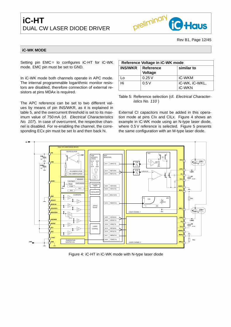
iC-WK MODE
Setting pin EMC = lo configures iC-HT for iC-WK
mode. EMC pin must be set to GND.
In iC-WK mode both channels operate in APC mode.
The internal programmable logarithmic monitor resis-
tors are disabled, therefore connection of external re-
sistors at pins MDAx is required.
The APC reference can be set to two different val-
ues by means of pin INS/WKR, as it is explained in
table 5, and the overcurrent threshold is set to its max-
imum value of 750 mA (cf. Electrical Characteristics
No. 107). In case of overcurrent, the respective chan-
nel is disabled. For re-enabling the channel, the corre-
sponding ECx pin must be set lo and then back hi.
Reference Voltage in iC-WK mode
INS/WKR Reference
Voltage
similar to
Lo 0.25 V iC-WKM
Hi 0.5 V iC-WK, iC-WKL,
iC-WKN
Table 5: Reference selection (cf. Electrical Character-
istics No. 110 )
External CI capacitors must be added in this opera-
tion mode at pins CIx and CILx. Figure 4 shows an
example in iC-WK mode using an N-type laser diode,
where 0.5 V reference is selected. Figure 5 presents
the same configuration with an M-type laser diode.
ADC2(7:0)
ADCC1(2:0)
0x10
0x1F
0x30
0x3F1μF
..10 nF..
VDD REGULATOR
TIMER
OSCILLATOR
LASER
RMD1(7:0)
0x16 ILIM2(7:0)
0x18 REF2(9:8)
0x19
0 255
PLR
CONTROL
0.25V/0.5V
0x17 RMD2(7:0)
INTEGRITYRAM
0x13
ILIM1(7:0)
R
OVT
MEMERR
IO DRIVERS
CFGTIMO
1μF
0x10
0x03 ADC1(9:8)
0x04
REGISTERS
ADC1(7:0)
0x05 ADC2(9:8)
0x06
MONITOR 8 Bit
CHECK
VB UNDERVOLTAGE
VDD UNDERVOLTAGE
OVC
PODO
SPI/I2CSLAVE
RAM
LASER CHANNEL 2
DUAL CW LASER DIODE DRIVER
RM1
RM2
ACC
APC
REF2(7:0)
WATCHDOG WATCHDOG
10 Bit
AD
8 Bit
AD
0x02 TEMP(7:0)
0x11
LASER CHANNEL 1
REF1(9:8)
0x14 REF1(7:0)
0x12
8 Bit
..10 nF..
TEMPERATURE
+
-
CI2
I LDK1
CI1
N
I LDK2
=1
+
-
NCVDD
CVB
OVC
AGND1
GND
VB
SCLK/SCL
LDK1
CIL1
VDD
GND
REF
NCHK
Check
VB
MRL2
MDA2
AGND2
CIL2
CI2
LDK2
DCO
EC2
EMC
NCS/A1
MOSI/A0
MISO/SDA
INS/WKR
NSTBY
EC1
T.PAD
CI1
MDA1
MRL1
=1
N
I LDK1
CI1
N
I LDK2
CI2
CVDD
CVB
Figure 4: iC-HT in iC-WK mode with N-type laser diode

preliminary
preliminary iC-HTDUAL CW LASER DIODE DRIVER
Rev B1, Page 13/45
IO DRIVERS
REGISTERS
REF2(9:8)
0x19
WATCHDOGTIMER
OSCILLATOR
LASER
CONTROL
0.25V/0.5V
APC
ACC
0x06 ADC2(7:0)
ADCC1(2:0)
0x10
..10 nF..
VDD REGULATOR
LASER CHANNEL 1
0x30
0x3F1μF
1μF
CFGTIMOWATCHDOG
0x17 RMD2(7:0)
INTEGRITYRAM
8 Bit
CHECK
0x14
ADC1(7:0)
LASER CHANNEL 2
DUAL CW LASER DIODE DRIVER
A
RM1
RM2
VB UNDERVOLTAGE
VDD UNDERVOLTAGE
OVC
PODOOVT
MEMERR
0x10
0x03 ADC1(9:8)
0x04
0x05 ADC2(9:8)
D
0x02 TEMP(7:0)
0x11 ILIM1(7:0)
0x13 REF1(9:8)
PLR
REF1(7:0)
0x12 RMD1(7:0)
0x16 ILIM2(7:0)
0x18
0x1F
REF2(7:0)
SPI/I2CSLAVE
RAM
10 Bit
AD
8 Bit
0 255
R
..10 nF..
TEMPERATUREMONITOR 8 Bit
CVDD
CVB
I LDK1
M
I LDK2
M
+
-
CI1
CI2
+
-=1
VDD
CIL1
MDA1
AGND1
LDK1
GND
VB
OVC
T.PAD
EC1
NSTBY
INS/WKR
MISO/SDA
SCLK/SCL
MOSI/A0
NCS/A1
EMC
EC2
DCO
CI1
LDK2
CI2
CIL2
AGND2
MDA2
MRL2
VB
Check
NCHK
MRL1
REF
GND
CI2
I LDK1
M
I LDK2
M
CVDD
CVB
CI1=1
Figure 5: iC-HT in iC-WK mode with M-type laser diode
In the configuration from figures 4 and 5 pin NSTBY is
connected to VB. This is required to force iC-HT leav-
ing standby mode and starting normal operation, as
the pin includes an internal pull-down resistor.
Laser channel enabling
Setting pins EC1, EC2 to hi enables the corresponding
channels. In order to ensure safe operation of iC-HT,
several events automatically disable both output chan-
nels:
• Pins INS/WKR or EMC left unconnected (IN-
SOPEN, EMCOPEN), iC-HT enters error mode
and the laser channels cannot be enabled.
• Supply power-down either at VB (PDOVB) or
VDD (PDOVDD), the laser channels are uncon-
ditionally disabled during the power down event.
• Overcurrent (OVC) or overtemperature (OVT),
laser channels are switched off. Cycling pins
EC1, EC2 or a power-up is required to switch on
the laser again.
preliminary
preliminary iC-HTDUAL CW LASER DIODE DRIVER
Rev B1, Page 14/45
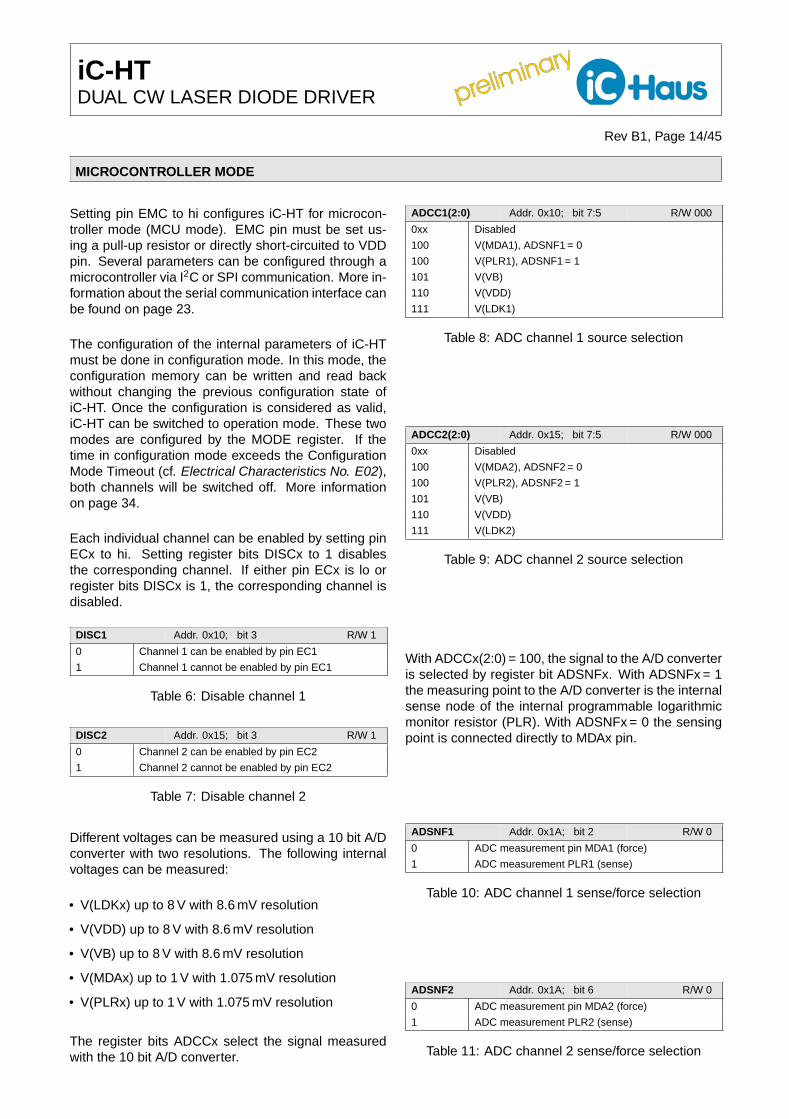
MICROCONTROLLER MODE
Setting pin EMC to hi configures iC-HT for microcon-
troller mode (MCU mode). EMC pin must be set us-
ing a pull-up resistor or directly short-circuited to VDD
pin. Several parameters can be configured through a
microcontroller via I2C or SPI communication. More in-
formation about the serial communication interface can
be found on page 23.
The configuration of the internal parameters of iC-HT
must be done in configuration mode. In this mode, the
configuration memory can be written and read back
without changing the previous configuration state of
iC-HT. Once the configuration is considered as valid,
iC-HT can be switched to operation mode. These two
modes are configured by the MODE register. If the
time in configuration mode exceeds the Configuration
Mode Timeout (cf. Electrical Characteristics No. E02),
both channels will be switched off. More information
on page 34.
Each individual channel can be enabled by setting pin
ECx to hi. Setting register bits DISCx to 1 disables
the corresponding channel. If either pin ECx is lo or
register bits DISCx is 1, the corresponding channel is
disabled.
DISC1 Addr. 0x10; bit 3 R/W 1
0 Channel 1 can be enabled by pin EC1
1 Channel 1 cannot be enabled by pin EC1
Table 6: Disable channel 1
DISC2 Addr. 0x15; bit 3 R/W 1
0 Channel 2 can be enabled by pin EC2
1 Channel 2 cannot be enabled by pin EC2
Table 7: Disable channel 2
Different voltages can be measured using a 10 bit A/D
converter with two resolutions. The following internal
voltages can be measured:
• V(LDKx) up to 8 V with 8.6 mV resolution
• V(VDD) up to 8 V with 8.6 mV resolution
• V(VB) up to 8 V with 8.6 mV resolution
• V(MDAx) up to 1 V with 1.075 mV resolution
• V(PLRx) up to 1 V with 1.075 mV resolution
The register bits ADCCx select the signal measured
with the 10 bit A/D converter.
ADCC1(2:0) Addr. 0x10; bit 7:5 R/W 000
0xx Disabled
100 V(MDA1), ADSNF1 = 0
100 V(PLR1), ADSNF1 = 1
101 V(VB)
110 V(VDD)
111 V(LDK1)
Table 8: ADC channel 1 source selection
ADCC2(2:0) Addr. 0x15; bit 7:5 R/W 000
0xx Disabled
100 V(MDA2), ADSNF2 = 0
100 V(PLR2), ADSNF2 = 1
101 V(VB)
110 V(VDD)
111 V(LDK2)
Table 9: ADC channel 2 source selection
With ADCCx(2:0) = 100, the signal to the A/D converter
is selected by register bit ADSNFx. With ADSNFx = 1
the measuring point to the A/D converter is the internal
sense node of the internal programmable logarithmic
monitor resistor (PLR). With ADSNFx = 0 the sensing
point is connected directly to MDAx pin.
ADSNF1 Addr. 0x1A; bit 2 R/W 0
0 ADC measurement pin MDA1 (force)
1 ADC measurement PLR1 (sense)
Table 10: ADC channel 1 sense/force selection
ADSNF2 Addr. 0x1A; bit 6 R/W 0
0 ADC measurement pin MDA2 (force)
1 ADC measurement PLR2 (sense)
Table 11: ADC channel 2 sense/force selection
preliminary
preliminary iC-HTDUAL CW LASER DIODE DRIVER
Rev B1, Page 15/45
0 255
R8 Bit
LASER CHANNEL 1
10 Bit
AD
8 Bit
AD
10 BitA
D
ACC
APC
RACC
RM1
PLR
..10 nF..
N
I LDK
CI1
MRL1
MDA1
AGND1
CIL1
CI1
LDK1
DCO
ECIE1
VB
VDD
LDK1
ADSNF1
OVC
DISP1
EMC
EACC1
+
-
N
I LDK
CI1
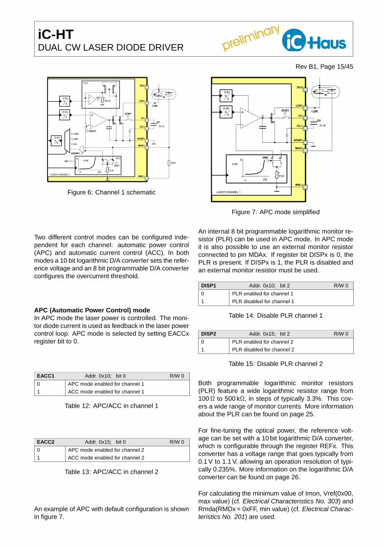
Figure 6: Channel 1 schematic
Two different control modes can be configured inde-
pendent for each channel: automatic power control
(APC) and automatic current control (ACC). In both
modes a 10 bit logarithmic D/A converter sets the refer-
ence voltage and an 8 bit programmable D/A converter
configures the overcurrent threshold.
APC (Automatic Power Control) mode
In APC mode the laser power is controlled. The moni-
tor diode current is used as feedback in the laser power
control loop. APC mode is selected by setting EACCx
register bit to 0.
EACC1 Addr. 0x10; bit 0 R/W 0
0 APC mode enabled for channel 1
1 ACC mode enabled for channel 1
Table 12: APC/ACC in channel 1
EACC2 Addr. 0x15; bit 0 R/W 0
0 APC mode enabled for channel 2
1 ACC mode enabled for channel 2
Table 13: APC/ACC in channel 2
An example of APC with default configuration is shown
in figure 7.
0 255
R8 Bit
8 Bit
10 Bit
LASER CHANNEL 1
A
..10 nF..
AD
D
PLR
CI1
+
-
I LDK
N
LDK1
CIL1
AGND1
MRL1
CI1CI
ECIE1
DCO
MDA1
EMC
I LDK
N
CI1
Figure 7: APC mode simplified
An internal 8 bit programmable logarithmic monitor re-
sistor (PLR) can be used in APC mode. In APC mode
it is also possible to use an external monitor resistor
connected to pin MDAx. If register bit DISPx is 0, the
PLR is present. If DISPx is 1, the PLR is disabled and
an external monitor resistor must be used.
DISP1 Addr. 0x10; bit 2 R/W 0
0 PLR enabled for channel 1
1 PLR disabled for channel 1
Table 14: Disable PLR channel 1
DISP2 Addr. 0x15; bit 2 R/W 0
0 PLR enabled for channel 2
1 PLR disabled for channel 2
Table 15: Disable PLR channel 2
Both programmable logarithmic monitor resistors
(PLR) feature a wide logarithmic resistor range from
100Ω to 500 kΩ, in steps of typically 3.3%. This cov-
ers a wide range of monitor currents. More information
about the PLR can be found on page 25.
For fine-tuning the optical power, the reference volt-
age can be set with a 10 bit logarithmic D/A converter,
which is configurable through the register REFx. This
converter has a voltage range that goes typically from
0.1 V to 1.1 V, allowing an operation resolution of typi-
cally 0.235%. More information on the logarithmic D/A
converter can be found on page 26.
For calculating the minimum value of Imon, Vref(0x00,
max value) (cf. Electrical Characteristics No. 303) and
Rmda(RMDx = 0xFF, min value) (cf. Electrical Charac-
teristics No. 201) are used.

preliminary
preliminary iC-HTDUAL CW LASER DIODE DRIVER
Rev B1, Page 16/45
Imon(min) = Vref (0x000,max)Rmda(RMDx =0xFF ,min)
= 0.11350000
= 0.31 uA
It is not recommended to configure iC-HT to have such
small Imon values, otherwise the leakage current at
MDAx may have an influence (cf. Electrical Charac-
teristics No. 204), especially at high temperatures. To
avoid this, Imon should be much greater than the leak-
age current.
For calculating the maximum value of Imon,
Vref(0x3FF, min value) (cf. Electrical Characteris-
tics No. 303) and Rmda(RMDx = 0x00, max vaule)
(cf. Electrical Characteristics No. 201) are used.
The following formula can to be used for calculating
Rmda(RMDx = 0x00, max value):
Rmd = Rmd0(1 + ∆ Rmd(%)100
)n+1, n from 0 to 255
Rmda(RMDx = 0x00, max) = Rmd0(1 + ∆ Rmd(%)100
)16
286 = Rmd0(1 + 3.3100
)16
Rmd0 = 170Ω
Therefore:
Imon(max) = Vref (0x3FF ,min)Rmd0
= 1.00170
= 5.88 mA
Any other Imon value can be calculated using Rmd for-
mula above. Due to its logarithmic characteristic, the
steps between two consecutive values is kept within
3.3 % typical value.
The programmable overcurrent shutdown can be set
to protect the laser by disabling the channel. The
overcurrent threshold is configurable in two different
ranges. The range is selected through register bit
RACCx. If RACCx = 1, the overcurrent threshold is in
the low range, up to 90 mA. If RACCx = 0, the overcur-
rent threshold is in the high range, up to 750 mA (cf.
Electrical Characteristics No. 107 ).
RACC1 Addr. 0x1A; bit 0 R/W 0
0 Current range high for channel 1
1 Current range low for channel 1
Table 16: RACC1 current range configuration channel
1
RACC2 Addr. 0x1A; bit 4 R/W 0
0 Current range high for channel 2
1 Current range low for channel 2
Table 17: RACC2 current range configuration channel
2
In each range, the particular overcurrent threshold
value can be set in register ILIMx. The regulator does
not differ the two current ranges in APC.
ILIM1 Addr. 0x11; bit 7:0 R/W 0xFF
0x0A Channel 1 overcurrent threshold set to minimum
current
. . . Channel 1 overcurrent threshold set to
Ilim = (∆I(LDK ) · n), n from 10 to 255
0xFF Channel 1 overcurrent threshold set to maximum
current
Table 18: Overcurrent threshold configuration channel
1
ILIM2 Addr. 0x16; bit 7:0 R/W 0xFF
0x0A Channel 2 overcurrent threshold set to minimum
current
. . . Channel 2 overcurrent threshold set to
Ilim = (∆I(LDK ) · n), n from 10 to 255
0xFF Channel 2 overcurrent threshold set to maximum
current
Table 19: Overcurrent threshold configuration channel
2
An overcurrent event can be simulated using SOVCx.
If SOVCx = 1, the corresponding overcurrent error bit
OVCx will be set to 1, the error will be signaled at
NCHK and the corresponding laser channel will be dis-
abled. The overcurrent error will remain forced until
SOVCx = 0.
SOVC1 Addr. 0x1D; bit 5 R/W 0
0 No Overcurrent event at channel 1 is simulated.
1 Overcurrent event at channel 1 simulated.
Table 20: Simulate overcurrent channel 1
SOVC2 Addr. 0x1D; bit 6 R/W 0
0 No overcurrent event at channel 2 is simulated.
1 Overcurrent event at channel 2 simulated.
Table 21: Simulate overcurrent channel 2

preliminary
preliminary iC-HTDUAL CW LASER DIODE DRIVER
Rev B1, Page 17/45
ACC (Automatic Current Control) mode
In this mode, the laser diode current is controlled and
no monitor diode is required. ACC mode is selected
setting EACCx register bit to 1.
EACC1 Addr. 0x10; bit 0 R/W 0
0 APC mode enabled for channel 1
1 ACC mode enabled for channel 1
Table 22: APC/ACC in channel 1
EACC2 Addr. 0x15; bit 0 R/W 0
0 APC mode enabled for channel 2
1 ACC mode enabled for channel 2
Table 23: APC/ACC in channel 2
In ACC mode the internal programmable logarithmic
monitor resistor (PLR) is not used. Instead the inter-
nal RACCx resistor is used to set the current. For
fine-tuning the regulated current, the reference volt-
age can be set with a 10 bit logarithmic D/A converter,
which is configurable through the register REFx. This
converter has a voltage range that goes typically from
0.1 V to 1.1 V, allowing an operation resolution of typi-
cally 0.235%. More information on the logarithmic D/A
converter can be found on page 26. Figure 8 shows an
example of this configuration.
Two different current ranges can be set through reg-
ister bit RACCx, with RACCx = 1 for up to 75 mA and
with RACCx = 0 for up to 650 mA. The programmable
overcurrent shutdown protects against over regula-
tions during the laser power-on. Table 44 shows some
typical current settings. For detailed limits, please refer
to Electrical Characteristics No. 114
ACC typical current settings
REFx RACCx=0 RACCx=1
0x000 77.0 mA 9.06 mA
0x001 77.2 mA 9.08 mA
0x010 77.4 mA 9.10 mA
... ... ...
0x200 256.2 mA 30.14 mA
0x201 256.8 mA 30.21 mA
0x202 257.4 mA 30.28 mA
... ... ...
0x3FD 846.0 mA 99.53 mA
0x3FE 848.0 mA 99.77 mA
0x3FF 850.0 mA 100 mA
Table 24: ACC typical current settings
ACC
APC
RACC
PLR1
..10 nF..
0 255
R8 Bit
LASER CHANNEL 1
10 Bit
AD
8 Bit
AD
10 BitA
D
+
-
I LDK
CI1
MRL1
MDA1
AGND1
CIL1
CI1
LDK1
DCO
ECIE1
VB
VDD
LDK1
ADSNF1
OVC
DISP1
EMC
I LDK
CI1
Figure 8: ACC mode simplified
RACC1 Addr. 0x1A; bit 0 R/W 0
0 Current range high for channel 1
1 Current range low for channel 1
Table 25: RACC1 configuration
RACC2 Addr. 0x1A; bit 4 R/W 0
0 Current range high for channel 2
1 Current range low for channel 2
Table 26: RACC2 configuration
In each range, the particular overcurrent threshold
value can be set in register ILIMx. The regulator does
differ the two current ranges in ACC.
ILIM1 Addr. 0x11; bit 7:0 R/W 0xFF
0x0A Channel 1 overcurrent threshold set to minimum
current
. . . Channel 1 overcurrent threshold set to
Ilim = (∆I(LDK ) · n), n from 10 to 255
0xFF Channel 1 overcurrent threshold set to maximum
current
Table 27: Overcurrent threshold configuration channel
1
ILIM2 Addr. 0x16; bit 7:0 R/W 0xFF
0x0A Channel 2 overcurrent threshold set to minimum
current
. . . Channel 2 overcurrent threshold set to
Ilim = (∆I(LDK ) · n), n from 10 to 255
0xFF Channel 2 overcurrent threshold set to maximum
current
Table 28: Overcurrent threshold configuration channel
2
An overcurrent event can be simulated using bit
SOVCx. If SOVCx = 1, the corresponding overcurrent

preliminary
preliminary iC-HTDUAL CW LASER DIODE DRIVER
Rev B1, Page 18/45
error bit OVCx will be set to 1, the error will be signaled
through NCHK and the corresponding laser channel
will be disabled. The overcurrent error will remain
forced until SOVCx = 0.
SOVC1 Addr. 0x1D; bit 5 R/W 0
0 No overcurrent event at channel 1 is simulated.
1 Overcurrent event at channel 1 simulated.
Table 29: Simulate overcurrent channel 1
SOVC2 Addr. 0x1D; bit 6 R/W 0
0 No overcurrent event at channel 2 is simulated.
1 Overcurrent event at channel 2 simulated.
Table 30: Simulate overcurrent channel 2
An external capacitor can be added in ACC mode in
order to avoid oscillations as it is shown in figure 8.
The external CIx must be enabled setting the ECIEx
bit (Tables 93 and 106).
In ACC mode, the MDAx pin can be monitored through
a 10 bit A/D converter. This can be used for measur-
ing the laser light power, if a photodiode is connected
to pin MDAx, as it is shown in figure 9. This allows ad-
justing the voltage reference in order to set the laser
current and obtain the desired laser light power.
The internal programmable logarithmic monitor Resis-
tor (PLR), if enabled (DISPx = 0), gives feedback for
the current control through the 10 bit A/D converter.
Register bit ADSNFx must be set to 1 in order to mea-
sure the internal sense node. An external monitor
resistor can be used to measure the optical power,
achieved by setting DISPx to 1. Therefore register bit
ADSNFx must be set to 0 in order to measure directly
at pin MDAx.
AD
10 BitA
D
ACC
APC
RACC1
..10 nF..
0 255 PLR1
R8 Bit
LASER CHANNEL 1
10 Bit
AD
8 Bit
+
-CI1
I LDK
N
MRL1
MDA1
AGND1
CIL1
CI1
LDK1
DCO
ECIE1
VB
VDD
LDK1
ADSNF1
OVC1
DISP1
EMC
N
CI1
I LDK
Figure 9: ACC with monitor photodiode
ACC mode permits to combine both channels in one
iC-HT (see chapter COMBINING BOTH CHANNELS)
and several iC-HT in parallel. When both channels are
combined the programmable overcurrent shutdown is
by channel. Another option is to connect the LDK
together when both channels are configured in ACC
mode and the channel 1 with high current range con-
figuration and the channel 2 with low current range
configuration. With this pre-sets there is a granularity
about 0.2% using the channel 1 steps regulation and
about 0.03% using the channel 2 in the regulation.
The Regulator
In MCU mode the control can be carried out without
the need of external capacitor. This allows a fast re-
sponse of the regulator. The speed of the regulator’s
response and stability can be configured using three
bits (COMPx), providing a compensation factor.
COMP1 Addr. 0x13; bit 6:4 R/W 011
000 Minimum compensation for the channel 1 regulator,
slower response of regulator
. . .
111 Maximum compensation for the channel 1
regulator, faster response of regulator
Table 31: Regulator delay compensation channel 1
COMP2 Addr. 0x18; bit 6:4 R/W 011
000 Minimum compensation for the channel 2 regulator,
slower response of regulator
. . .
111 Maximum compensation for the channel 2
regulator, faster response of regulator
Table 32: Regulator delay compensation channel 2
Alternatively it is possible to use external capacitors
connected to pins CIx and CILx. In this case, register
bit ECIEx should be set to 1 and COMPx to its highest
value, "111".
ECIE1 Addr. 0x10; bit 1 R/W 0
0 External CI capacitor for channel 1 disconnected
1 External CI capacitor for channel 1 connected
Table 33: Enable external capacitor channel 1
ECIE2 Addr. 0x15; bit 1 R/W 0
0 External CI capacitor for channel 2 disconnected
1 External CI capacitor for channel 2 connected
Table 34: Enable external capacitor channel 2
The regulator is offset compensated in order to pre-
vent optical power drifts. Offset compensation can be
disabled by setting register bit EOCx to 0.
preliminary
preliminary iC-HTDUAL CW LASER DIODE DRIVER
Rev B1, Page 19/45
EOC1 Addr. 0x10; bit 4 R/W 1
0 Channel 1 regulator offset compensation disabled
1 Channel 1 regulator offset compensation enabled
Table 35: Enable offset compensation channel 1
EOC2 Addr. 0x15; bit 4 R/W 1
0 Channel 2 regulator offset compensation disabled
1 Channel 2 regulator offset compensation enabled
Table 36: Enable offset compensation channel 2
An internal oscillator is used for the offset compensa-
tion. A watchdog timer (WDT) is included in order to
monitor proper function of the oscillator. If an error
is detected by the WDT, the laser channels are dis-
abled, OSCERR error bit is set in STATUS0 register
and the error event is signaled at pin NCHK. This error
signaling can be suppressed using the mask register
bit MOSCERR (set to 1).
MOSCERR Addr. 0x1D; bit 0 R/W 0
0 Oscillator error (watchdog) will be signaled at
NCHK
1 Oscillator error (watchdog) will not be signaled at
NCHK
Table 37: Oscillator error mask
iC-HT monitors the saturation voltage of the regula-
tor´s output transistor at pin LDKx. The LDK satura-
tion threshold can be configured through register bits
RLDKSx.
RLDKS1 Addr. 0x13; bit 3:2 R/W 00
00 V(LDK1) < 0.5 V sets the LDKSAT1 alarm bit
01 V(LDK1) < 0.8 V sets the LDKSAT1 alarm bit
10 V(LDK1) < 1.0 V sets the LDKSAT1 alarm bit
11 V(LDK1) < 1.2 V sets the LDKSAT1 alarm bit
Table 38: LDK saturation threshold selection channel
1
RLDKS2 Addr. 0x18; bit 3:2 R/W 00
00 V(LDK2) < 0.5 V sets the LDKSAT2 alarm bit
01 V(LDK2) < 0.8 V sets the LDKSAT2 alarm bit
10 V(LDK2) < 1.0 V sets the LDKSAT2 alarm bit
11 V(LDK2) < 1.2 V sets the LDKSAT2 alarm bit
Table 39: LDK saturation threshold selection channel
2
If the LDKx voltage falls below the LDK saturation
threshold the LDKSATx error bit in STATUS1 register
will be set and it will be signaled through output pin
NCHK. Setting the mask register bit MLDKSATx to 1
suppresses the signaling at NCHK.
MLDKSAT1 Addr. 0x1D; bit 2 R/W 1
0 LDKSAT1 event will be signaled at NCHK
1 LDKSAT1 event will not be signaled at NCHK
Table 40: LDK saturation mask channel 1
MLDKSAT2 Addr. 0x1D; bit 3 R/W 1
0 LDKSAT2 event will be signaled at NCHK
1 LDKSAT2 event will not be signaled at NCHK
Table 41: LDK saturation mask channel 2
Laser channel enabling and error handling
With pin INS/WKR or EMC unconnected, a corre-
sponding error signal will be generated (INSOPEN,
EMCOPEN) and will disable the laser channels. Any
input interface could be enabled if EMC or INS pins
are open. Comunication with the chip might be possi-
ble but laser cannot be switched on. This situation is
only signaled at the MCU interruption pin NCHK, which
would remain low as long as any of the EMC or INS
pins are unconnected. MCU must monitor the status
of the NCHK pin to get all the status information of the
chip
Setting DISC1 and DISC2 to 1(default) disables the
corresponding channel.
The errors in STATUS0 and STATUS1 registers disable
the laser channels. Every change in the STATUS reg-
isters is signaled at pin NCHK, unless the error event
is masked by the corresponding error mask bit.

preliminary
preliminary iC-HTDUAL CW LASER DIODE DRIVER
Rev B1, Page 20/45
Register Address Bits Default Description
INITRAM 0x00 0 R/O RAM initialized.
PDOVDD 0x00 1 R/O Power down event at VDD
MEMERR 0x00 2 R/O RAM memory validation error
OVT 0x00 3 R/O Overtemperature event
OVC2 0x00 4 R/O Overcurrent at channel 2
OVC1 0x00 5 R/O Overcurrent at channel 1
OSCERR 0x00 6 R/O Oscillator error (watchdog set)
CFGTIMO 0x00 7 R/O Configuration mode timeout event
MAPC1 0x01 0 R/O Channel 1 current state (on or off)
MONC1 0x01 1 R/O Monitor channel 1 enabled at least once (latched)
LDKSAT1 0x01 2 R/O Channel 1 LDK saturation event
MAPC2 0x01 4 R/O Channel 2 current state (on or off)
MONC2 0x01 5 R/O Monitor channel 2 enabled at least once (latched)
LDKSAT2 0x01 6 R/O Channel 2 LDK saturation event
Table 42: Status registers overview
In order to enable the channels, the error events must
be acknowledged. Acknowledging an error is accom-
plished by reading the STATUS register. After a power-
on PDVDD and INITRAM errors will be set, therefore
it is required to read STATUS0 and STATUS1 registers
after each power-on.
Exiting standby mode will not reset the RAM but will
set the PDOVDD status bit. Therefore STATUS0 must
be read once after each standby to re-enable the laser
channels.
In case of an overcurrent (OVC) or an overtemperature
(OVT) event, laser channels are disabled.
A memory error event and a configuration timeout er-
ror event will also disable the laser channels. More
information about the memory error on page 34. The
conditions to enable each laser channel are shown in
figure 10.
2
7
56
1
4
STATUS0 (Addr. 0x00)
0PDOVDDMEMERR
(Addr. 0x10 )
1
Pin
OVC2
CFGTIMO
(Addr. 0x15 )
Pin
3
INITRAM
OVT
OVC1
1
1
&
DISC2
INSOPENEMCOPEN
EC2
MAPC1
DISC1
EC1
MAPC2
&
1
&
1
1
1
&
1
Figure 10: Laser control logic in MCU mode
preliminary
preliminary iC-HTDUAL CW LASER DIODE DRIVER
Rev B1, Page 21/45
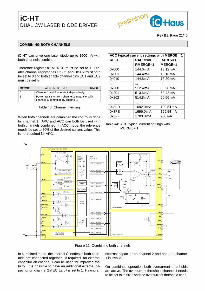
COMBINING BOTH CHANNELS
iC-HT can drive one laser diode up to 1500 mA with
both channels combined.
Therefore register bit MERGE must be set to 1. Dis-
able channel register bits DISC1 and DISC2 must both
be set to 0 and both enable channel pins EC1 and EC2
must be set hi.
MERGE Addr. 0x1B; bit 6 R/W 0
0 Channel 1 and 2 operate independently
1 Power transistor from channel 2 in parallel with
channel 1, controlled by channel 1
Table 43: Channel merging
When both channels are combined the control is done
by channel 1. APC and ACC can both be used with
both channels combined. In ACC mode, the reference
needs be set to 50% of the desired current value. This
is not required for APC.
ACC typical current settings with MERGE = 1
REF1 RACCx=0 RACCx=1
RMERGE=1 MERGE=1
0x000 144.0 mA 18.12 mA
0x001 144.4 mA 18.16 mA
0x010 144.8 mA 18.20 mA
... ... ...
0x200 512.4 mA 60.28 mA
0x201 513.6 mA 60.42 mA
0x202 514.8 mA 60.56 mA
... ... ...
0x3FD 1692.0 mA 199.54 mA
0x3FE 1696.0 mA 199.54 mA
0x3FF 1700.0 mA 200 mA
Table 44: ACC typical current settings with
MERGE = 1
REF2(7:0)
PLR1
DA
A
10 Bit
ADCC1(2:0)
DUAL CW LASER DIODE DRIVER
0x14
CFGTIMOWATCHDOG WATCHDOG
TIMER
OSCILLATOR
LASER
CONTROL
0x13 REF1(9:8)
RMD1(7:0)
D
REGISTERS
SPI/I2C
TEMP(7:0)
0x11 ILIM1(7:0)
0x05 ADC2(9:8)
0x06 ADC2(7:0)
RAM
LASER CHANNEL 1
R
DA
8 Bit
OVC
MEMERR
0x19
RMD2(7:0)
INTEGRITY
OVT 0x04 ADC1(7:0)
0x10
0x1F
0x30
0x3F
0x16
LASER CHANNEL 2
VDD REGULATOR
TEMPERATURE 0x02
1μF
2550
RM1
0x03 ADC1(9:8)
..10 nF..
0x10
10 Bit
APC
8 Bit
ACC
IO DRIVERS
SLAVE
RAM
REF1(7:0)
0x12
1μF
ILIM2(7:0)
CHECK
VB UNDERVOLTAGE
VDD UNDERVOLTAGE
PODO
MONITOR 8 Bit
0x18 REF2(9:8)
0x17
=1
I LDK
N
+
-CI1
CVB CVDD
+
-
GND
VDD
VBREF
ADSNF1
EACC1
OVC1
DISP1
EMC
MDA1
AGND2
LDK2
CI
VB
LDK1
CIL1
AGND1
CI2
MDA2
CIL2
MRL2
MRL1
CI1
CI ECIE1
DCO
GND
Check
NCHK
EC1
NSTBY
INS/WKR
MISO/SDA
SCLK/SCL
MOSI/A0
NCS/A1
EC2
VDD
VB
LDK1
EMC
T.PAD
=1
I LDK
NCVB CVDD
CI1
Figure 11: Combining both channels
In combined mode, the internal CI nodes of both chan-
nels are connected together. If required, an external
capacitor on channel 1 can be used for improved sta-
bility. It is possible to have an additional external ca-
pacitor on channel 2 if ECIE2 bit is set to 1. Having an
external capacitor on channel 2 and none on channel
1 is invalid.
On combined operation both overcurrent thresholds
are active. The overcurrent threshold channel 1 needs
to be set to to 50% and the overcurrent threshold chan-

preliminary
preliminary iC-HTDUAL CW LASER DIODE DRIVER
Rev B1, Page 22/45
nel 2 should be disabled by setting it to its maximum
value (0xFF). An overcurrent will only be detected on
channel 1.
ILIM1 Addr. 0x11; bit 7:0 R/W 0xFF
0x0A Channel 1 overcurrent threshold: 80 mA,
MERGE=1
. . . Channel 1 overcurrent threshold set to
Ilim = (2 ∗∆I(LDK ) · n), n from 10 to 255,
MERGE=1
0xFF Channel 1 overcurrent threshold: 2040 mA,
MERGE=1
Table 45: Overcurrent threshold configuration channel
1 with MERGE = 1
It is possible to use a second photodiode connected
to channel 2 (e.g. as a safety supervisor). The ADC
on channel 2 can be used to monitor the voltage at pin
MDA2, as it is shown in figure 12.
ADC1(7:0)
0x05 ADC2(9:8)
0x06 ADC2(7:0)
1μF
CFGTIMOWATCHDOG WATCHDOG
TIMER
0x16 ILIM2(7:0)
0x18
0 255
OSCILLATOR
LASER
CONTROL
ACC
APC
PLR1
REF2(9:8)
0x19 REF2(7:0)
0x17 RMD2(7:0)
INTEGRITYRAM
CHECK
VB UNDERVOLTAGE
VDD UNDERVOLTAGE
OVC
PODOOVT
MEMERR
10 BitA
D
0x10
0x03 ADC1(9:8)
0x04
VDD REGULATOR
LASER CHANNEL 1
LASER CHANNEL 2
DUAL CW LASER DIODE DRIVER
RM1
ADCC1(2:0)
0x10
0x1F
0x30
0x3F1μF
IO DRIVERS
REGISTERS
SPI/I2CSLAVE
RAM
10 Bit
AD
8 Bit
AD
0x02 TEMP(7:0)
0x11 ILIM1(7:0)
0x13 REF1(9:8)
0x14 REF1(7:0)
0x12 RMD1(7:0)
R8 Bit
..10 nF..
TEMPERATUREMONITOR 8 Bit
+
-
CVB CVDD
+
-
N
I LDK
CI1=1
INS/WKR
NSTBY
EC1
VB
VDD
LDK1
GND
T.PAD
EACC1
ADSNF1
OVC1
DISP1
EMC
CI
AGND1
CILDK1
VB
CIL1
VDD
GND
REF
MRL1
NCHK
Check
VB
MRL2
MDA2
AGND2
CIL2
CI2
LDK2
MDA1
CI1
ECIE1
DCO
EC2
EMC
NCS/A1
MOSI/A0
SCLK/SCL
MISO/SDA
CVDDCVBN
I LDK
CI1=1
Figure 12: Additional photodiode in combined configuration
preliminary
preliminary iC-HTDUAL CW LASER DIODE DRIVER
Rev B1, Page 23/45
SERIAL COMMUNICATION INTERFACES
SPI slave interface
The SPI slave interface is enabled by setting pin
INS/WKR to lo and uses pins NCS/A1, SCLK/SCL,
MISO/SDA and MOSI/A0. Pin NCS/A1 is the chip se-
lect pin and must be set lo by the SPI master in order
to start communication. Pins MISO/SDA and MOSI/A0
are the data communication lines and pin SCLK/SCL
is the clock line generated by the SPI master (e.g. mi-
crocontroller). The SPI protocol frames are shown in
figure 13.
A communication frame consists of one address byte
and at least one data byte. Bits 7:6 of the address byte
is the opcode used for selecting a read operation (set
to "10") or a write (set to "01") operation. The remain-
ing 6 bits are used for register addressing.
It is possible to transmit several bytes consecutively,
if the NCS signal is not reset and SCLK/SCL keeps
clocking, as it is shown in figure 13. The address is in-
ternally incremented after each transmitted byte. Once
the address reaches the last register (0x3F), it is reset
back to 0x00.
13 14 15
MOSI
SPI READ COMMAND FRAME. OPCODE = 10, POLARITY = 0, PHASE = 0
SPI WRITE COMMAND FRAME. OPCODE = 01, POLARITY = 0, PHASE = 0
NCS
Don't care
16 17
Data n HIZMISO HIZ (Pull-Up) Don't care Data 1 MSB first Data 2
Init Addr.(5:0) MSB first
SCLK 0 1 2 3 4 5 6 7 8 9 10 11 12 13 14 15
MOSI
0 1SCLK
Data 1 MSB first Data 2
16 17
Data n Don't care
MISO HIZ (Pull-Up) Don't care
NCS
2
Init Addr.(5:0) MSB first
3 4 5 6 7 8 9 10 11 12
Figure 13: SPI read and write commands
I2C slave interface
The I2C slave interface is enabled by setting pin
INS/WKR to hi and uses pins NCS/A1, SCLK/SCL,
MISO/SDA and MOSI/A0. The protocol frames are
shown in figure 14.
A communication frame consists of one slave address
byte, one register address byte and at least one data
byte. Bits 7:1 of the slave address byte form the slave
identification code (ID) and bit 0 is used for specifica-
tion of the data direction (0 for write, 1 for read). The
slave ID consists of 7 bits. The five most significant bits
are fixed by default to value 0b11000. Pins MOSI/A0
and NCS/A1 are used to set the remaining slave ID
bits (see table 46 and 47).
Action b7 b6 b5 b4 b3 b2 b1 b0
Write to slave 1 1 0 0 0 A1 A0 0
Read from slave 1 1 0 0 0 A1 A0 1
Table 46: I2C write/read byte
Action A1 A0 Slave ID Address byte
Write to slave 0 lo lo 0x60 0xC0
Read from slave 0 lo lo 0x60 0xC1
Write to slave 1 lo hi 0x61 0xC2
Read from slave 1 lo hi 0x61 0xC3
Write to slave 2 hi lo 0x62 0xC4
Read from slave 2 hi lo 0x62 0xC5
Write to slave 3 hi hi 0x63 0xC6
Read from slave 3 hi hi 0x63 0xC7
Table 47: I2C write/read address

preliminary
preliminary iC-HTDUAL CW LASER DIODE DRIVER
Rev B1, Page 24/45
37
Data 2
38
Stop
Data n
A1:A0
0 4 5 6 7 8 9 10 11
A1:A0
Slave ACKWR='0'
Addr. MSB first
Start
0 1 2 3
WR='0' Repeated Start
4 5 6 7 8 9 10 11 12 13 14 15
SDA
16
Slave ACK
2120
Data 1 Data 2
28
17
I2C READ COMMAND FRAME.
1
Addr. MSB first
Start
SCL
Slave ACK
Data 1
34 35
Master ACK
36
2
Slave ACK
I2C WRITE COMMAND FRAME.
3 12 13 14 15
SDA
16 17
18
25 26 27
A1:A0
RD='1'
Data 1
28
Slave ACK
18
Stop
Data 1
19
.
SCL 19
Data n
25 26 27
Slave ACK
Figure 14: I2C read and write commands

preliminary
preliminary iC-HTDUAL CW LASER DIODE DRIVER
Rev B1, Page 25/45
8 BIT INTERNAL PROGRAMMABLE LOGARITHMIC MONITOR RESISTORS
In MCU mode internal 8 bit programmable logarithmic
monitor resistors (PLRx) are provided for APC.
The resistor value can be selected from 256 values,
ranging from 100Ω to 500 kΩ, following logarithmic in-
crements with a typical step width of 3.3%. The resis-
tors are configured with registers RMDx(7:0).
RMD1 Addr. 0x12; bit 7:0 R/W 0xFF
0x00 PLR1 set to the minimum resistance
. . . PLR1 set to
Rmd = Rmd0(1 +∆ Rmd(%)
100)n+1, n from 0 to 255
0xFF PLR1 resistor set to the maximum resistance
Table 48: MDA resistor channel 1
RMD2 Addr. 0x17; bit 7:0 R/W 0xFF
0x00 PLR2 resistor set to the minimum resistance
. . . PLR2 set to
Rmd = Rmd0(1 +∆ Rmd(%)
100)n+1, n from 0 to 255
0xFF PLR2 resistor set to the maximum resistance
Table 49: MDA resistor channel 2
The following formula calculates the register RMDx in
order to set the desired resistor value:
Rmd = Rmd0(1 + ∆ Rmd(%)100
)n+1, n from 0 to 255
Where Rmd0 is the minimum resistor value (typically
100Ω), ∆Rmd(%) is the step between two consecu-
tive resistor values (typically 3.3%) and n is the value
of RMDx register in decimal.
In APC mode the regulation node is the internal con-
nection to PLR, it is not MDAx pin. Voltage present at
pin MDAx may differ from the internal regulation node.
This regulation node can be sensed through the 10 bit
A/D converter and read at register ADCx. Register bit
ADSNFx must be set to 1 for this purpose. If ADSNFx
is set to 0, MDAx pin will be the input of the A/D con-
verter.
At pin MDAx only the 4 MSB of the RMDx configu-
ration from PLRx are measurable. The 8 bits of the
PLRx configuration RMDx can be measured with the
A/D converter setting ADSNFx to 1.
The PLRx can be disabled using register bit DISPx.
With DISPx = 0 the PLRx is enabled and DISPx = 1
disables the PLRx.
DISP1 Addr. 0x10; bit 2 R/W 0
0 PLR enabled for channel 1
1 PLR disabled for channel 1
Table 50: Disable PLR channel 1
DISP2 Addr. 0x15; bit 2 R/W 0
0 PLR enabled for channel 2
1 PLR disabled for channel 2
Table 51: Disable PLR channel 2
R8 Bit
LASER CHANNEL 1
10 Bit
AD
8 Bit
AD
10 Bit
PLR1
APC
..10 nF..
AD
N
I LDK
+
-
0 255
CI1
MRL1
MDA1
CIL1
CI1
LDK1
DCO
ECIE1
VB
VDD
LDK1
ADSNF1
DISP1
EMC
AGND1
N
I LDK
CI1
Figure 15: PLR in APC
In ACC mode the PLR is not used in the control cir-
cuit. Instead, the internal RACCx resistor is used in
the control loop.
Even though the PLR is not in the control circuit, it
can be enabled (DISPx = 0) in order to give feedback
through the 10 bit A/D converter for the controlling light
power if a monitor diode is connected.
Register bit ADSNF is set to 1 to measure the internal
sense node. Alternatively, an external monitor resistor
can be used to measure the optical power, by setting
DISPx to 1. Then register bit ADSNF must be set to 0
in order to measure directly at pin MDAx.

preliminary
preliminary iC-HTDUAL CW LASER DIODE DRIVER
Rev B1, Page 26/45
AD
10 BitA
D
ACC
APC
RACC1
..10 nF..
0 255 PLR1
R8 Bit
LASER CHANNEL 1
10 Bit
AD
8 Bit
+
-CI1
I LDK
N
MRL1
MDA1
AGND1
CIL1
CI1
LDK1
DCO
ECIE1
VB
VDD
LDK1
ADSNF1
OVC1
DISP1
EMC
N
CI1
I LDK
Figure 16: ACC with monitor photodiode
10 BIT LOGARITHMIC D/A CONVERTER
The 10 bit logarithmic D/A converter is used for set-
ting the regulator´s voltage reference. The D/A con-
verter is active in all operating modes. In iC-WK mode
only two values are available: 0.25 V (setting INS/WKR
pin lo) and 0.5 V (setting INS/WKR pin hi). In MCU
mode both APC and ACC use the D/A converter. With
a range from 0.1 V to 1.1 V and the typical step width
is 0.235%.
The D/A converter is configured through register
REFx(9:0). With REFx(9:0) = 0x000, D/A output value
is set to 0.1 V, and for REFx(9:0) = 0x3FF, D/A output
is configured to 1.1 V.
REF1 Addr. 0x13/14; bit 9:0 R/W 0x000
0x000 Channel 1 regulator reference voltage set to
minimum voltage
. . . Channel 1 regulator reference voltage set to
Vref = Vref0(1 +∆ Vref (%)
100)n+1, n from 0 to 1023
0x3FF Channel 1 regulator reference voltage set to
maximum voltage
Table 52: Channel 1 regulator voltage reference
REF2 Addr. 0x18/19; bit 9:0 R/W 0x000
0x000 Channel 2 regulator reference voltage set to
minimum voltage
. . . Channel 2 regulator reference voltage set to
Vref = Vref0(1 +∆ Vref (%)
100)n+1, n from 0 to 1023
0x3FF Channel 2 regulator reference voltage set to
maximum voltage
Table 53: Channel 2 regulator voltage reference
To calculate the D/A converter value for each REFx
value, use the following formula:
Vref = Vref0(1 + ∆ Vref (%)100
)n+1, n from 0 to 1023
Where Vref0 is the minimum value (typically 0.1 V),
∆Vref (%) is the step value (typically 0.235 %) and n
is the value of REFx register in decimal.
preliminary
preliminary iC-HTDUAL CW LASER DIODE DRIVER
Rev B1, Page 27/45
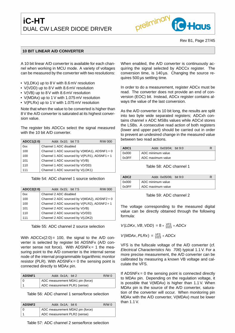
10 BIT LINEAR A/D CONVERTER
A 10 bit linear A/D converter is available for each chan-
nel when working in MCU mode. A variety of voltages
can be measured by the converter with two resolutions:
• V(LDKx) up to 8 V with 8.6 mV resolution
• V(VDD) up to 8 V with 8.6 mV resolution
• V(VB) up to 8 V with 8.6 mV resolution
• V(MDAx) up to 1 V with 1.075 mV resolution
• V(PLRx) up to 1 V with 1.075 mV resolution
Note that when the value to be converted is higher than
8 V the A/D converter is saturated at its highest conver-
sion value.
The register bits ADCCx select the signal measured
with the 10 bit A/D converter.
ADCC1(2:0) Addr. 0x10; bit 7:5 R/W 000
0xx Channel 1 ADC disabled
100 Channel 1 ADC sourced by V(MDA1), ADSNF1 = 0
100 Channel 1 ADC sourced by V(PLR1), ADSNF1 = 1
101 Channel 1 ADC sourced by V(VB)
110 Channel 1 ADC sourced by V(VDD)
111 Channel 1 ADC sourced by V(LDK1)
Table 54: ADC channel 1 source selection
ADCC2(2:0) Addr. 0x15; bit 7:5 R/W 000
0xx Channel 2 ADC disabled
100 Channel 2 ADC sourced by V(MDA2), ADSNF2 = 0
100 Channel 2 ADC sourced by V(PLR2), ADSNF2 = 1
101 Channel 2 ADC sourced by V(VB)
110 Channel 2 ADC sourced by V(VDD)
111 Channel 2 ADC sourced by V(LDK2)
Table 55: ADC channel 2 source selection
With ADCCx(2:0) = 100, the signal to the A/D con-
verter is selected by register bit ADSNFx (A/D con-
verter sense not force). With ADSNFx = 1 the mea-
suring point to the A/D converter is the internal sense
node of the internal programmable logarithmic monitor
resistor (PLR). With ADSNFx = 0 the sensing point is
connected directly to MDAx pin.
ADSNF1 Addr. 0x1A; bit 2 R/W 0
0 ADC measurement MDA1 pin (force)
1 ADC measurement PLR1 (sense)
Table 56: ADC channel 1 sense/force selection
ADSNF2 Addr. 0x1A; bit 6 R/W 0
0 ADC measurement MDA2 pin (force)
1 ADC measurement PLR2 (sense)
Table 57: ADC channel 2 sense/force selection
When enabled, the A/D converter is continuously ac-
quiring the signal selected by ADCCx register. The
conversion time, is 140 µs. Changing the source re-
quires 500 µs settling time.
In order to do a measurement, register ADCx must be
read. The converter does not provide an end of con-
version (EOC) bit. Instead, ADCx register contains al-
ways the value of the last conversion.
As the A/D converter is 10 bit long, the results are split
into two byte wide separated registers; ADCxh con-
tains channel x ADC MSBs values while ADCxl stores
the LSBs. A consecutive read action of both registers
(lower and upper part) should be carried out in order
to prevent an undesired change in the measured value
between two read actions.
ADC1 Addr. 0x03/04; bit 9:0 R
0x000 ADC minimum value
0x3FF ADC maximum value
Table 58: ADC channel 1
ADC2 Addr. 0x05/06; bit 9:0 R
0x000 ADC minimum value
0x3FF ADC maximum value
Table 59: ADC channel 2
The voltage corresponding to the measured digital
value can be directly obtained through the following
formula:
V (LDKx , VB, VDD) = 8 ∗ VFS1023
∗ ADCx
V (MDAx , PLRx) = VFS1023
∗ ADCx
VFS is the fullscale voltage of the A/D converter (cf.
Electrical Characteristics No. 706) typical 1.1 V. For a
more precise measurement, the A/D converter can be
calibrated by measuring a known VB voltage and cal-
culate the VFS.
If ADSNFx = 0 the sensing point is connected directly
to MDAx pin. Depending on the regulation voltage, it
is possible that V(MDAx) is higher than 1.1 V. When
MDAx pin is the source of the A/D converter, satura-
tion of the converter will occur. When monitoring pin
MDAx with the A/D converter, V(MDAx) must be lower
than 1.1 V.

preliminary
preliminary iC-HTDUAL CW LASER DIODE DRIVER
Rev B1, Page 28/45
DC/DC CONVERTER OPTIMIZATION
iC-HT provides a 6 bit configurable current at pin DCO
that can be used to trim the output voltage of a DC/DC
converter.
Possible application benefits with using DCO:
• DC/DC step down operation: regulation at voltages
lower than power supply
• DC/DC step up operation: regulation at voltages
higher than power supply
• Efficiency enhancement
RDCO Addr. 0x1B; bit 5:0 R/W 0x02
0x00 No current
. . .
0x3F 130 µA typ (cf. Electrical Characteristics No. D01)
Table 60: Digital current output register
The proposed applications can be demonstrated with
a standard DC/DC converter e.g. TPS63060DSC from
Texas Instruments. This converter allows an input volt-
age ranging from 2.5 V to 12 V and offers an output
voltages from 2.5 V to 8 V. It is capable of delivering up
to 2 A current, depending on the output voltage. Figure
17 shows a possible configuration.
R1
R2
TPS63060
2x10μF 0.1μF
3x22μF
R31MEG
C1 C3
C2
L1
VIN
EN
VAUX
PS/SYNC
GND
L2
VOUT
FB
PG
PGND
2.5...12VVin
Vout
1μH
L1L1
1μH
C1 C3
C21MEGR3
Figure 17: TPS63063 DC/DC converter from TI
DC/DC step down operation:
regulation at voltages lower than power supply
The resistors R1 and R2 in the feedback path allow
setting the desired output value Vout. The DC/DC con-
verter drives Vout pin in order to yield 0.5 V at feed-
back pin FB. The DCO output signal from iC-HT is
connected to FB pin. The Vout is controlled with the
internal register RDCO from iC-HT.
The DCO current into FB node controls the voltages
of the divider R1 and R2 and Vout changes in order to
maintain 0.5 V at FB pin. Selecting R1 and R2 needs
to consider:
• Resistors values:
R1 = R2( VoutVfb
− 1)
• Current of the voltage divider should be high enough,
in comparism to the current from the pin DCO, to of-
fer acceptable resolution. The programmable current
resolution from register RDCO is 2 µA.
• DCO current into the voltage divider will lower Vout
voltage, Vout is 8 V when no current is present at
DCO.
Choosing R1 to 100 kΩ, the value of R2 can be calcu-
lated:
R2 = R1VoutVfb
−1= 100k
80.5
−1= 6.7kΩ
With this configuration the current through the voltage
divider is 75 µA at 8 V . The resolution of each RDCO
step is then 200 mV.

preliminary
preliminary iC-HTDUAL CW LASER DIODE DRIVER
Rev B1, Page 29/45
The value in RDCO register needed in order to have
the desired output voltage can be calculated using the
following formula:
RDCO = Idco2uA
= IR2−IR12uA
=0.5
6.7k− Vout−0.5
100k
2uA
The resulting value will vary slightly depending on the
tolerances of the selected resistors and DCO current.
The voltage is reduced from 8 V (RDCO = 0) to 2.5 V,
when RDCO = 27.
DC/DC step up operation: regulation at voltages
higher than power supply
A practical application of the present case is the con-
trol of blue lasers. This type of laser present a forward
voltage around 5 V, which demands an LDA voltage of
about 6 V. If the system is supplied with a 3 V LiPo bat-
tery, it is necessary to use a the DC/DC in order to step
up and drive the laser diode and driver with a sufficient
voltage. Figure 18 shows this application:
0.1μF
3x22μF
R1 R3
R2
100k
6.7k
1MEG
0x19 REF2(7:0)
0x17 RMD2(7:0)
INTEGRITY
OVT 0x04 ADC1(7:0)
0x10
0x1F
0x30
0x3F
0x16
LASER CHANNEL 2
VDD REGULATOR
TEMPERATURE
REF1(9:8)
RMD1(7:0)
0x02
2550
MEMERR
0x03 ADC1(9:8)
0x10
10 Bit
D
8 Bit
A
IO DRIVERS
A
PLR1
D
REGISTERS
SPI/I2C
TEMP(7:0)
0x11 ILIM1(7:0)
0x05 ADC2(9:8)
0x06 ADC2(7:0)
LASER CHANNEL 1
DOVC
10 Bit
APC
ACC
SLAVE
RAM
2x10μF
ILIM2(7:0)
CHECK
VB UNDERVOLTAGE
VDD UNDERVOLTAGE
RAM
PODO
0x13
MONITOR 8 Bit
A
8 Bit
0x18 REF2(9:8)
R
REF1(7:0)
0x12
1μF
ADCC1(2:0)
DUAL CW LASER DIODE DRIVER
0x14
CFGTIMOWATCHDOG WATCHDOG
TIMER
OSCILLATOR
LASER
CONTROL
TPS63060
1μF
+
-
N
CVB
CVDD
+
-
20μA
=1
C2
C3
1μH
L1
C1
GND
3VVB
VDD
VBREF
ADSNF1
OVC1
DISP1
EMC
MDA1
MISO/SDA
SCLK/SCL
GND
PS/SYNC
VAUX
PG
VIN
L1
EN
FB
PGND
L2
VOUT6V
LDK1
CIL1
AGND1
LDK2
CI2
AGND2
MDA2
CIL2
MRL2
MRL1
CI1CI
ECIE1
DCO
GND
Check
NCHK
EC1
NSTBY
INS/WKR
MOSI/A0
NCS/A1
EC2
VDD
VB
LDK1
EMC
T.PAD
CVB
CVDDN
20μA
=1
L1
1μH
C1
C2
C3
Figure 18: Regulation at voltage greater than power supply
Setting register RDCO to 10 it delivers 20 µA and 6 V
are obtained at Vout.
Extension of system working voltage range
iC-HT must be supplied by a voltage within the thresh-
old values of 2.8 V and 8 V. It is possible to control the
DC/DC output in a voltage range of 2.5 V - 12 V if the
DC/DC converter, controlled by DCO output signal, is
included in the system, as it is shown in figure 19:
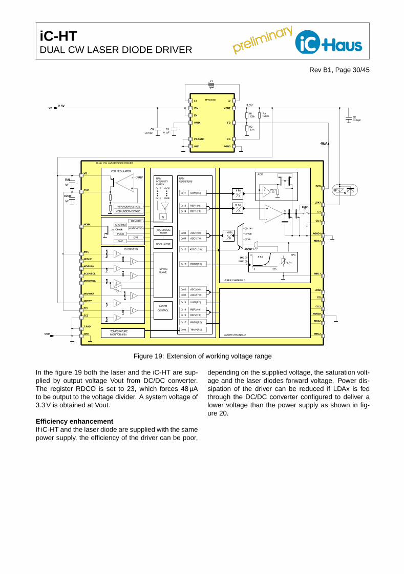
preliminary
preliminary iC-HTDUAL CW LASER DIODE DRIVER
Rev B1, Page 30/45
VB UNDERVOLTAGE
VDD UNDERVOLTAGE
RAM
PODO
0x13
MONITOR 8 Bit
A
8 Bit
0x18 REF2(9:8)
R
REF1(7:0)
0x12
1μF
ADCC1(2:0)
DUAL CW LASER DIODE DRIVER
0x14
CFGTIMOWATCHDOG WATCHDOG
TIMER
OSCILLATOR
LASER
CONTROL
TPS63060
1μF
0
0x03 ADC1(9:8)
0x10
10 Bit
D
8 Bit
A
IO DRIVERS
A
PLR1
D
REGISTERS
SPI/I2C
TEMP(7:0)
0x11 ILIM1(7:0)
0x05 ADC2(9:8)
0x06 ADC2(7:0)
LASER CHANNEL 1
DOVC
10 Bit
APC
ACC
SLAVE
RAM
2x10μF
ILIM2(7:0)
0.1μF
CHECK
3x22μF
R1 R3
R2
100k
6.7k
1MEG
0x19 REF2(7:0)
0x17 RMD2(7:0)
INTEGRITY
OVT 0x04 ADC1(7:0)
0x10
0x1F
0x30
0x3F
0x16
LASER CHANNEL 2
VDD REGULATOR
TEMPERATURE
REF1(9:8)
RMD1(7:0)
0x02
255
MEMERR
C3
L1
1μH
C1
C2
=1
+
-
48μA
+
-
N
CVB
CVDD
GND
VB2.5V 3.3V
VDD
VBREF
ADSNF1
OVC1
DISP1
EMC
MDA1
MISO/SDA
SCLK/SCL
GND
PS/SYNC
VAUX
PG
VIN
L1
EN
FB
PGND
L2
VOUT
LDK1
CIL1
AGND1
LDK2
CI2
AGND2
MDA2
CIL2
MRL2
MRL1
CI1CI
ECIE1
DCO
GND
Check
NCHK
EC1
NSTBY
INS/WKR
MOSI/A0
NCS/A1
EC2
VDD
VB
LDK1
EMC
T.PAD
1μH
L1
C1
C2
C3
=1
48μA
CVB
CVDDN
Figure 19: Extension of working voltage range
In the figure 19 both the laser and the iC-HT are sup-
plied by output voltage Vout from DC/DC converter.
The register RDCO is set to 23, which forces 48 µA
to be output to the voltage divider. A system voltage of
3.3 V is obtained at Vout.
Efficiency enhancement
If iC-HT and the laser diode are supplied with the same
power supply, the efficiency of the driver can be poor,
depending on the supplied voltage, the saturation volt-
age and the laser diodes forward voltage. Power dis-
sipation of the driver can be reduced if LDAx is fed
through the DC/DC converter configured to deliver a
lower voltage than the power supply as shown in fig-
ure 20.

preliminary
preliminary iC-HTDUAL CW LASER DIODE DRIVER
Rev B1, Page 31/45
R1 R3
R2
100k
6.7k
1MEG
0x19 REF2(7:0)
0x17 RMD2(7:0)
INTEGRITY
OVT 0x04 ADC1(7:0)
0x10
0x1F
0x30
0x3F
0x16
LASER CHANNEL 2
VDD REGULATOR
TEMPERATURE
REF1(9:8)
RMD1(7:0)
0x02
255
MEMERR
ADC1(9:8)
0x10
10 Bit
D
8 Bit
A
IO DRIVERS
A
PLR1
D
REGISTERS
SPI/I2C
TEMP(7:0)
0x11 ILIM1(7:0)
0x05 ADC2(9:8)
0x06 ADC2(7:0)
LASER CHANNEL 1
DOVC
10 Bit
APC
ACC
SLAVE
RAM
2x10μF
ILIM2(7:0)
0.1μF
CHECK
3x22μF
VB UNDERVOLTAGE
VDD UNDERVOLTAGE
RAM
PODO
0x13
MONITOR 8 Bit
A
8 Bit
0x18 REF2(9:8)
R
REF1(7:0)
0x12
1μF
ADCC1(2:0)
DUAL CW LASER DIODE DRIVER
0x14
CFGTIMOWATCHDOG WATCHDOG
TIMER
OSCILLATOR
LASER
CONTROL
TPS63060
1μF
0
0x03
+
-
CVDDN
CVB
+
-
48μA
=1
C3
1μH
L1
C1
C2
GND
5VVB
3.3V
VDD
VBREF
ADSNF1
OVC1
DISP1
EMC
MDA1
MISO/SDA
SCLK/SCL
GND
PS/SYNC
VAUX
PG
VIN
L1
EN
FB
PGND
L2
VOUT
LDK1
CIL1
AGND1
LDK2
CI2
AGND2
MDA2
CIL2
MRL2
MRL1
CI1CI
ECIE1
DCO
GND
Check
NCHK
EC1
NSTBY
INS/WKR
MOSI/A0
NCS/A1
EC2
VDD
VB
LDK1
EMC
T.PAD
CVB
CVDDN
48μA
=1
L1
1μH
C1
C2
C3
Figure 20: System efficiency enhancement
The register RDCO is set to 23 to provide a laser diode
supply voltage of 3.3 V at Vout.

preliminary
preliminary iC-HTDUAL CW LASER DIODE DRIVER
Rev B1, Page 32/45
WATCHDOG TIMER
The internal 200 kHz oscillator is monitored with the
Watchdog Timer (WDT).
If the oscillator remains longer than the maximum time
of tWDT (cf. Electrical Characteristics No. E03) with-
out activity an oscillator error is triggered. An oscillator
error sets OSCERR error bit to 1. The automatic offset
compensation of the laser control requires the oscilla-
tor.
The state of OSCERR is signaled at pin NCHK. The
signaling of OSCERR state can be masked with bit
MOSCERR. Setting MOSCERR to 1 masks the oscil-
lator error and OSCERR will not be signaled at NCHK.
It is possible to simulate an error of the oscillator us-
ing SOSCERR bit. If SOSCERR = 1, the oscillator er-
ror is forced. When OSCERR is set to 1 the error will
be signaled through NCHK, depending on the state of
MOSCERR.
OSCERR Addr. 0x00; bit 6 R
0 Oscillator operates OK
1 Watchdog timeout set, oscillator fail. Cleared on
read
Table 61: Oscillator error
MOSCERR Addr. 0x1D; bit 0 R/W 0
0 Oscillator error (watchdog) will be signaled at
NCHK
1 Oscillator error (watchdog) will not be signaled at
NCHK
Table 62: Oscillator error mask
SOSCERR Addr. 0x1D; bit 7 R/W 0
0 No oscillator error simulated.
1 Oscillator error simulated (watchdog timeout).
Table 63: Simulate oscillator error

preliminary
preliminary iC-HTDUAL CW LASER DIODE DRIVER
Rev B1, Page 33/45
TEMPERATURE MONITOR AND PROTECTION
iC-HT includes an 8 bit temperature monitor that al-
lows to measure the internal chip temperature going
from -40 °C to 125 °C. The resolution is 1 °C/LSB. The
internal temperature can be obtained by reading TEMP
register. The TEMP register is a read-only register.
TEMP Addr. 0x02; bit 7:0 R
0x00 Minimum temperature
. . .
0xFF Maximum temperature
Table 64: Chip temperature
Absolute read values may differ from one chip to an-
other. An individual initial calibration of the temper-
ature monitor is recommended. The TEMP register
must be read at a known temperature. Using the reso-
lution value of 1 °C/LSB, the internal temperature can
be calculated.
The temperature monitor can be used to compensate
temperature effects on the laser diode. The microcon-
troller can use a laser diode characteristic formula or
a look-up table combined with the temperature value
measured through TEMP register. The reference volt-
age can be configured accordingly in order to compen-
sate temperature effects.
iC-HT is protected against overtemperature. In iC-
WK mode, if the internal temperature value exceeds
the overtemperature threshold an OVT error event will
be triggered and signaled through pin NCHK. Both
laser channels will be disabled. Pin NCHK will keep
signaling the error although the internal temperature
goes down to a safe value below the overtemperature
threshold value. If the temperature has exceeded the
overtemperature threshold value, pins EC1 and EC2
have to be pulled lo in order to stop signaling the error.
Setting pin ECx back hi will re-enable the correspond-
ing channel.
In microcontroller mode, if the internal temperature
exceeds a safety value an overtemperature error bit
(OVT) will be set to 1. If OVT = 1, both channels will be
disabled and the error event will be signaled through
NCHK pin. If the internal temperature goes down to a
safe value below the overtemperature threshold value,
OVT will remain at value 1. Reading the OVT bit stop
signaling error through pin NCHK. Reading OVT bit will
set it back to 0. Setting ECx pin lo and then back hi will
allow re-enabling the corresponding channel.
The overtemperature threshold value can not be con-
figured.
OVT Addr. 0x00; bit 3 R
0 No overtemperature event has occurred since last
read
1 Overtemperature event has occurred. Cleared on
read
Table 65: Overtemperature detection
In microcontroller mode it is possible to simulate an
overtemperature event using SOVT bit. Setting SOVT
to 1, the overtemperature error flag OVT will be set to
1. iC-HT will remain in error state until SOVT is set
back to 0.
SOVT Addr. 0x1D; bit 4 R/W 0
0 No overtemperature event is simulated.
1 Overtemperature event simulated.
Table 66: Simulate overtemperature

preliminary
preliminary iC-HTDUAL CW LASER DIODE DRIVER
Rev B1, Page 34/45
DIGITAL INTERFACE AND MEMORY INTEGRITY MONITOR
iC-HT provides a microcontroller slave interface by se-
lection on the EMC pin. iC-HT support the interfaces
SPI or I2C that are selected by the INS/WKR pin.
EMC Addr. Pin;
lo iC-WK-mode, digital interfaces disabled
Open Not allowed, error signaled
hi MCU mode, interface selected by INS/WKR
enabled
Table 67: Enable microcontroller
INS/WKR Addr. Pin;
lo SPI interface selected
Open Not allowed, error signaled.
hi I2C interface selected
Table 68: Interface selection I2C or SPI
The configuration memory is integrity monitored and
atomic executable (all at once: changes of the config-
urations without any direct effects, the changes are ex-
ecuted at once by command ) to the functional blocks
of iC-HT.
Integrity monitoring is implemented by a duplication of
the configuration registers into a validation page (see
description below) where the register are automatically
copied with inverted value. Every register bit is com-
pared with its validation copy and in case of difference,
a memory error is generated and both laser channels
are switched off.
Atomic appliance is achieved by latching the configu-
ration registers. This permits a full configuration (differ-
ent registers) to be made prior to apply it to the laser
channels. iC-HT has two different modes selectable by
the MODE(1:0) register (address 0x1C).
MODE(1:0) Addr. 0x1C; bit 1:0 R/W 01
00 Invalid parameter
01 Operation mode
10 Configuration mode
11 Invalid parameter
Table 69: Configuration and operation mode
In Configuration mode, the configuration memory
(address 0x10 to 0x1F) can be written and read back
to check a correct communication without changing the
present configured operation state of the iC-HT. In this
mode, the memory integrity check is disabled.
iC-HT will monitor the time elapsed in configuration
mode and automatically switch the laser off if it ex-
ceeds a configuration mode timeout. The time in con-
figuration mode must less than 40 ms for ensuring that
no configuration timeout occurs during configuration
(cf. Electrical Characteristics No. E02). The timeout
can be up to 164 ms.
When writing the configuration is completed, iC-HT is
switched to operation mode by writing "10" into the
MODE register (address 0x1C). In operation mode
the configuration is applied to the iC-HT and the mem-
ory integrity check activated. In this mode configura-
tion registers can only be read (except MODE(1:0) reg-
ister, which is always accessible). Figure 21 shows the
interface to memory structure.
RNW
RNW_RAM
MEMERR
LATCH
CFG(127:0)
CHECKERROR
DB(7:0)
RAM
Addr. Decoder
RNW_VAL
VALIDATION
SPI / I2C
Addr. 0x1C
0x10
0x1F
MODE
0x30
0x3F
ADR(6:0)
&&
Figure 21: Interface, RAM integrity monitoring and configuration latching

preliminary
preliminary iC-HTDUAL CW LASER DIODE DRIVER
Rev B1, Page 35/45
Register map description
The register map consists of 64 addresses subdivided
in three different pages:
• Read-only page, address 0x00 to 0x0F: iC-HT
status, ADC readouts, thermometer readout and
chip revision.
• Configuration page (integrity monitored), read-
write registers, address 0x10 to 0x1F.
• Validation page, read-write registers, address
0x30 to 0x3F.
Read-only registers
Read-only registers are sub-divided as well into sta-
tus registers (address 0x00 to 0x01) and measurement
registers. Status registers are normally latched to 1 on
events and cleared on read (see individual register de-
scription). Measurement registers are dual-port and
can be accessed simultaneously with the measure-
ments in progress. ADC1(address 0x03 to 0x04) and
ADC2 (address 0x05 to 0x06) are 10 bit registers split
into two 8 bit registers each and must be accessed in
block mode (automatic address increment) to ensure
data not changing during the read.
Configuration page (integrity monitored)
The configuration page (address 0x10 to 0x1F) con-
tains the registers that control the driver. Every write
operation to any of the registers of this page will be
internally duplicated to the correspondent register at
the validation page. After the write operation, the cor-
respondent validation register will contain the inverted
value of the configuration register.
Validation page
The validation page (address 0x30 to 0x3F) can be
read or written normally. Only when a write procedure
is made to any of the configuration registers the corre-
spondent validation pair will be written with the inverted
value of the configuration register as well.
Both the configuration and validation pages are initial-
ized during power-up. This event is signaled at the
STATUS0 register (bit 0, INITRAM). In standby mode
(NSTBY = lo) the RAM is not reset if any write com-
mand has been executed and therefore, configuration
and validation pages keep the stored information and
INITRAM remains unset. Entering standby mode af-
ter power-up without any write command, the RAM will
be initialized again and the INITRAM bit will be set to
1 again. Any VDD power-down event signaled at the
STATUS0 register outside the standby mode (NSTBY =
hi) requires a RAM content check regardless of the
state of the INITRAM bit to ensure data is not cor-
rupted.
Possible start-up sequence:
1. iC-HT starts in operation mode with default con-
figuration. INITRAM and PDOVDD error bits
must be set in STATUS0, DISC1 (address 0x10,
bit 3) and DISC2 (address 0x15, bit 3) are set to
1.
2. Write MODE(1:0) = "10" register (Addr. 0x1C) to
enable the configuration mode.
3. Configure the laser channels.
4. Read back to verify a correct data transfer.
5. Set the DISC1, DISC2 bits to 0 on used chan-
nels.
6. Read the status registers(address 0x00, 0x01,
0x02) to detect possible errors and validate sta-
tus. If any error exist, read again to ensure its
validation.
7. Write MODE(1:0) = "01" register (address 0x1C)
to apply the configuration and enable the mem-
ory integrity check.
8. During operation: monitor the status registers
checking for errors. The NCHK pin signals any
set status bit if not masked. This pin can be used
to trigger an microcontroller interrupt line.

preliminary
preliminary iC-HTDUAL CW LASER DIODE DRIVER
Rev B1, Page 36/45
START-UP
Setting pin NSTBY to lo iC-HT enters standby mode.
In stand by mode and with no supply voltage at pin
VDD and the current consumption on VB is reduced to
less than 10 µA (cf. Electrical Characteristics No. 002).
After wake-up (pin NSTBY rising edge), the internal
regulated supply VDD is generated again. The re-
quired time Tvdd depends on the capacitor connected
to the VDD pin (cf. Electrical Characteristics No. 504).
Once the VDD voltage level is correct, iC-HT enters an
offset compensation procedure regardless of the state
of the laser enable pins (EC1, EC2). During this time
(Ten), EC1 and EC2 are ignored and laser cannot be
switched on (cf. Electrical Characteristics No. 111). Af-
ter this time (Ten), laser channels can be switched on.
The switch-on procedure needs an initial time (Tci) to
reach the 80 % of the target light power (in APC mode)
or laser current (in ACC mode) (cf. Electrical Char-
acteristics No. 112) and an additional time (Tcio) to
reach the 99 % of the value (cf. Electrical Characteris-
tics No. 113 ). Figure 22 illustrates an startup example
for channel 1 in iC-WK mode.
NSTBY
VDDOK
EC1
I(LDK1)
VDD
Tci TcioTen
TVdd
Figure 22: Startup timing diagram
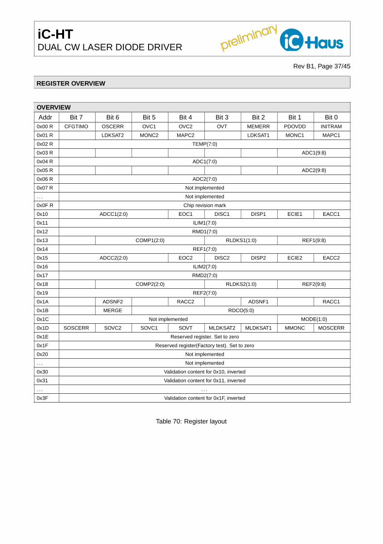
preliminary
preliminary iC-HTDUAL CW LASER DIODE DRIVER
Rev B1, Page 37/45
REGISTER OVERVIEW
OVERVIEW
Addr Bit 7 Bit 6 Bit 5 Bit 4 Bit 3 Bit 2 Bit 1 Bit 0
0x00 R CFGTIMO OSCERR OVC1 OVC2 OVT MEMERR PDOVDD INITRAM
0x01 R LDKSAT2 MONC2 MAPC2 LDKSAT1 MONC1 MAPC1
0x02 R TEMP(7:0)
0x03 R ADC1(9:8)
0x04 R ADC1(7:0)
0x05 R ADC2(9:8)
0x06 R ADC2(7:0)
0x07 R Not implemented
. . . Not implemented
0x0F R Chip revision mark
0x10 ADCC1(2:0) EOC1 DISC1 DISP1 ECIE1 EACC1
0x11 ILIM1(7:0)
0x12 RMD1(7:0)
0x13 COMP1(2:0) RLDKS1(1:0) REF1(9:8)
0x14 REF1(7:0)
0x15 ADCC2(2:0) EOC2 DISC2 DISP2 ECIE2 EACC2
0x16 ILIM2(7:0)
0x17 RMD2(7:0)
0x18 COMP2(2:0) RLDKS2(1:0) REF2(9:8)
0x19 REF2(7:0)
0x1A ADSNF2 RACC2 ADSNF1 RACC1
0x1B MERGE RDCO(5:0)
0x1C Not implemented MODE(1:0)
0x1D SOSCERR SOVC2 SOVC1 SOVT MLDKSAT2 MLDKSAT1 MMONC MOSCERR
0x1E Reserved register. Set to zero
0x1F Reserved register(Factory test). Set to zero
0x20 Not implemented
. . . Not implemented
0x30 Validation content for 0x10, inverted
0x31 Validation content for 0x11, inverted
. . . . . .
0x3F Validation content for 0x1F, inverted
Table 70: Register layout
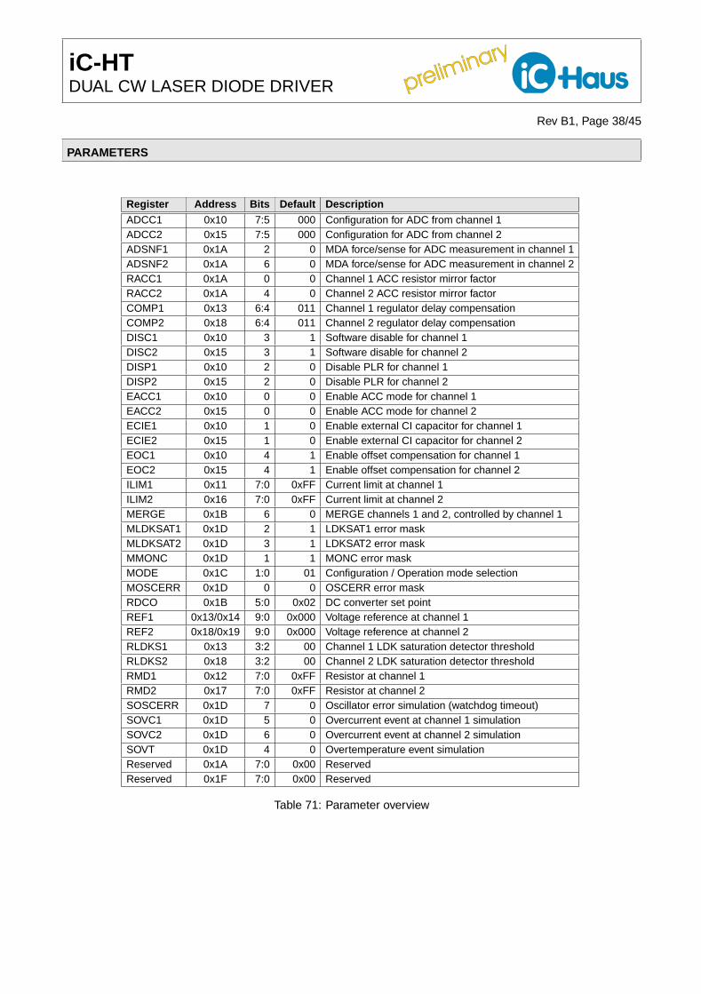
preliminary
preliminary iC-HTDUAL CW LASER DIODE DRIVER
Rev B1, Page 38/45
PARAMETERS
Register Address Bits Default Description
ADCC1 0x10 7:5 000 Configuration for ADC from channel 1
ADCC2 0x15 7:5 000 Configuration for ADC from channel 2
ADSNF1 0x1A 2 0 MDA force/sense for ADC measurement in channel 1
ADSNF2 0x1A 6 0 MDA force/sense for ADC measurement in channel 2
RACC1 0x1A 0 0 Channel 1 ACC resistor mirror factor
RACC2 0x1A 4 0 Channel 2 ACC resistor mirror factor
COMP1 0x13 6:4 011 Channel 1 regulator delay compensation
COMP2 0x18 6:4 011 Channel 2 regulator delay compensation
DISC1 0x10 3 1 Software disable for channel 1
DISC2 0x15 3 1 Software disable for channel 2
DISP1 0x10 2 0 Disable PLR for channel 1
DISP2 0x15 2 0 Disable PLR for channel 2
EACC1 0x10 0 0 Enable ACC mode for channel 1
EACC2 0x15 0 0 Enable ACC mode for channel 2
ECIE1 0x10 1 0 Enable external CI capacitor for channel 1
ECIE2 0x15 1 0 Enable external CI capacitor for channel 2
EOC1 0x10 4 1 Enable offset compensation for channel 1
EOC2 0x15 4 1 Enable offset compensation for channel 2
ILIM1 0x11 7:0 0xFF Current limit at channel 1
ILIM2 0x16 7:0 0xFF Current limit at channel 2
MERGE 0x1B 6 0 MERGE channels 1 and 2, controlled by channel 1
MLDKSAT1 0x1D 2 1 LDKSAT1 error mask
MLDKSAT2 0x1D 3 1 LDKSAT2 error mask
MMONC 0x1D 1 1 MONC error mask
MODE 0x1C 1:0 01 Configuration / Operation mode selection
MOSCERR 0x1D 0 0 OSCERR error mask
RDCO 0x1B 5:0 0x02 DC converter set point
REF1 0x13/0x14 9:0 0x000 Voltage reference at channel 1
REF2 0x18/0x19 9:0 0x000 Voltage reference at channel 2
RLDKS1 0x13 3:2 00 Channel 1 LDK saturation detector threshold
RLDKS2 0x18 3:2 00 Channel 2 LDK saturation detector threshold
RMD1 0x12 7:0 0xFF Resistor at channel 1
RMD2 0x17 7:0 0xFF Resistor at channel 2
SOSCERR 0x1D 7 0 Oscillator error simulation (watchdog timeout)
SOVC1 0x1D 5 0 Overcurrent event at channel 1 simulation
SOVC2 0x1D 6 0 Overcurrent event at channel 2 simulation
SOVT 0x1D 4 0 Overtemperature event simulation
Reserved 0x1A 7:0 0x00 Reserved
Reserved 0x1F 7:0 0x00 Reserved
Table 71: Parameter overview

preliminary
preliminary iC-HTDUAL CW LASER DIODE DRIVER
Rev B1, Page 39/45
Register Address Bits Default Description
INITRAM 0x00 0 R/O RAM initialized.
PDOVDD 0x00 1 R/O Power-down event at VDD
MEMERR 0x00 2 R/O RAM memory validation error
OVT 0x00 3 R/O Overtemperature event
OVC2 0x00 4 R/O Overcurrent at channel 2
OVC1 0x00 5 R/O Overcurrent at channel 1
OSCERR 0x00 6 R/O Oscillator error (watchdog set)
CFGTIMO 0x00 7 R/O Configuration mode timeout event
MAPC1 0x01 0 R/O Channel 1 current state
MONC1 0x01 1 R/O Monitor channel 1 enabled at least once (latched)
LDKSAT1 0x01 2 R/O Channel 1 LDK saturation event
MAPC2 0x01 4 R/O Channel 2 current state
MONC2 0x01 5 R/O Monitor channel 2 enabled at least once (latched)
LDKSAT2 0x01 6 R/O Channel 2 LDK saturation event
Table 72: Status overview
Register Address Bits Default Description
TEMP 0x02 7:0 R/O Chip temperature measurement
ADC1h 0x03 1:0 R/O Channel 1 ADC 9:8 readout
ADC1l 0x04 7:0 R/O Channel 1 ADC 7:0 readout
ADC2h 0x05 1:0 R/O Channel 2 ADC 9:8 readout
ADC2l 0x06 7:0 R/O Channel 2 ADC 7:0 readout
CHIPREV 0x0F 7:0 R/O Chip revision identification
Table 73: Measurement overview
Device identification
CHIPREV Addr. 0x0F; bit 7:0 R
0x00 Initial version iC-HT
0x01 iC-HT_1
0x02 iC-HT_Z
0x08 Reserved
Table 74: Device identification
Status
INITRAM Addr. 0x00; bit 0 R
0 RAM not initialized since last read
1 RAM initialized. Cleared on read
Table 75: RAM initialization
PDOVDD Addr. 0x00; bit 1 R
0 VDD power down not occurred since last read
1 VDD power down event has occurred. Cleared on
read
Table 76: VDD power down
MEMERR Addr. 0x00; bit 2 R
0 RAM has not been changed since last validation
1 RAM has changed and has not been validated
Table 77: Memory validation
OVT Addr. 0x00; bit 3 R
0 No overtemperature event has occurred since last
read
1 Overtemperature event has occurred. Cleared on
read
Table 78: Overtemperature
OVC2 Addr. 0x00; bit 4 R
0 No overcurrent event at channel 2 has occurred
since last read
1 Overcurrent event at channel 2 has occurred.
Cleared on read
Table 79: Overcurrent channel 2

preliminary
preliminary iC-HTDUAL CW LASER DIODE DRIVER
Rev B1, Page 40/45
OVC1 Addr. 0x00; bit 5 R
0 No overcurrent event at channel 1 has occurred
since last read
1 Overcurrent event at channel 1 has occurred.
Cleared on read
Table 80: Overcurrent channel 1
OSCERR Addr. 0x00; bit 6 R
0 Oscillator functioning OK
1 Watchdog timeout set on oscillator failure.
Cleared on read
Table 81: Oscillator watchdog
CFGTIMO Addr. 0x00; bit 7 R
0 iC-HT not in Configuration Mode or Timeout did not
happened till now
1 iC-HT in Configuration Mode and Timeout
happened. Laser switched off.
Table 82: Configuration timeout
MAPC1 Addr. 0x01; bit 0 R
0 Channel 1 is off at the precise reading moment
1 Channel 1 is on at the precise reading moment
Table 83: EC1 pin state
MONC1 Addr. 0x01; bit 1 R
0 Channel 1 has not been switched on since last read
1 Channel 1 has been switched on at least once.
Cleared on read
Table 84: Monitor channel 1
LDKSAT1 Addr. 0x01; bit 2 R
0 Channel 1 LDK saturation voltage not reached.
1 Channel 1 LDK saturation voltage reached at least
once, cleared on read
Table 85: LDK1 saturation
MAPC2 Addr. 0x01; bit 4 R
0 Channel 1 is off at the precise reading moment
1 Channel 1 is on at the precise reading moment
Table 86: EC2 pin state
MONC2 Addr. 0x01; bit 5 R
0 Channel 2 has not been switched on since last read
1 Channel 2 has not been switched on since last read
Table 87: Monitor channel 2
LDKSAT2 Addr. 0x01; bit 6 R
0 Channel 2 LDK saturation voltage not reached.
1 Channel 2 LDK saturation voltage reached at least
once, Cleared on read
Table 88: LDK2 saturation
Measurement registers
TEMP Addr. 0x02; bit 7:0 R
0x00 Minimum temperature
0xFF Maximum temperature
Table 89: Chip temperature
ADC1 Addr. 0x03/04; bit 9:0 R
0x000 ADC minimum value
0x3FF ADC maximum value
Table 90: ADC channel 1
ADC2 Addr. 0x05/06; bit 9:0 R
0x000 ADC minimum value
0x3FF ADC maximum value
Table 91: ADC channel 2
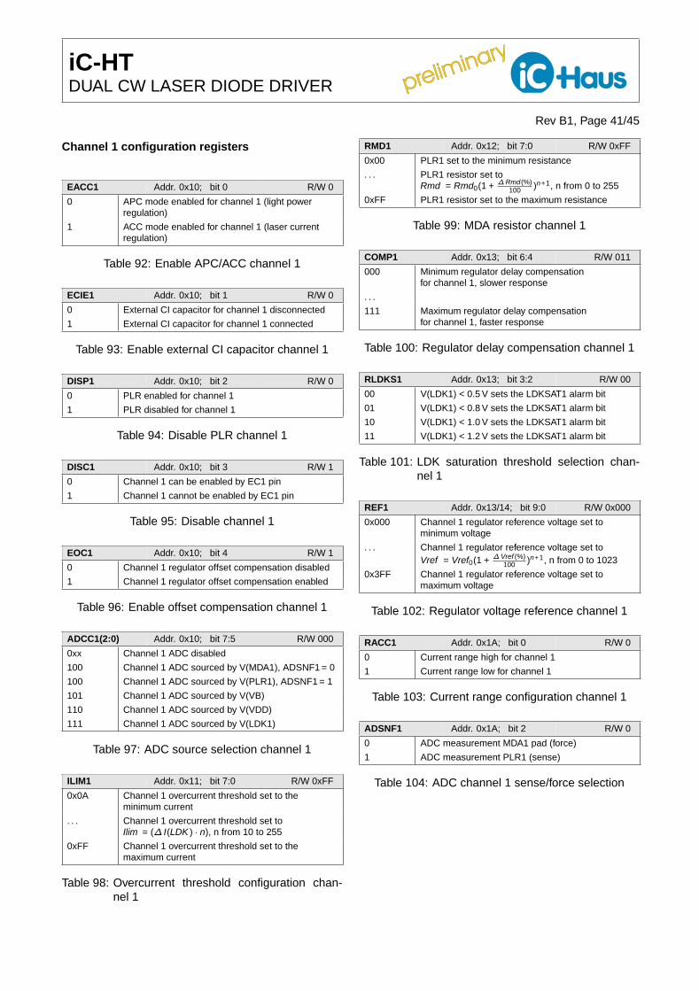
preliminary
preliminary iC-HTDUAL CW LASER DIODE DRIVER
Rev B1, Page 41/45
Channel 1 configuration registers
EACC1 Addr. 0x10; bit 0 R/W 0
0 APC mode enabled for channel 1 (light power
regulation)
1 ACC mode enabled for channel 1 (laser current
regulation)
Table 92: Enable APC/ACC channel 1
ECIE1 Addr. 0x10; bit 1 R/W 0
0 External CI capacitor for channel 1 disconnected
1 External CI capacitor for channel 1 connected
Table 93: Enable external CI capacitor channel 1
DISP1 Addr. 0x10; bit 2 R/W 0
0 PLR enabled for channel 1
1 PLR disabled for channel 1
Table 94: Disable PLR channel 1
DISC1 Addr. 0x10; bit 3 R/W 1
0 Channel 1 can be enabled by EC1 pin
1 Channel 1 cannot be enabled by EC1 pin
Table 95: Disable channel 1
EOC1 Addr. 0x10; bit 4 R/W 1
0 Channel 1 regulator offset compensation disabled
1 Channel 1 regulator offset compensation enabled
Table 96: Enable offset compensation channel 1
ADCC1(2:0) Addr. 0x10; bit 7:5 R/W 000
0xx Channel 1 ADC disabled
100 Channel 1 ADC sourced by V(MDA1), ADSNF1 = 0
100 Channel 1 ADC sourced by V(PLR1), ADSNF1 = 1
101 Channel 1 ADC sourced by V(VB)
110 Channel 1 ADC sourced by V(VDD)
111 Channel 1 ADC sourced by V(LDK1)
Table 97: ADC source selection channel 1
ILIM1 Addr. 0x11; bit 7:0 R/W 0xFF
0x0A Channel 1 overcurrent threshold set to the
minimum current
. . . Channel 1 overcurrent threshold set to
Ilim = (∆ I(LDK ) · n), n from 10 to 255
0xFF Channel 1 overcurrent threshold set to the
maximum current
Table 98: Overcurrent threshold configuration chan-
nel 1
RMD1 Addr. 0x12; bit 7:0 R/W 0xFF
0x00 PLR1 set to the minimum resistance
. . . PLR1 resistor set to
Rmd = Rmd0(1 +∆ Rmd(%)
100)n+1, n from 0 to 255
0xFF PLR1 resistor set to the maximum resistance
Table 99: MDA resistor channel 1
COMP1 Addr. 0x13; bit 6:4 R/W 011
000 Minimum regulator delay compensation
for channel 1, slower response
. . .
111 Maximum regulator delay compensation
for channel 1, faster response
Table 100: Regulator delay compensation channel 1
RLDKS1 Addr. 0x13; bit 3:2 R/W 00
00 V(LDK1) < 0.5 V sets the LDKSAT1 alarm bit
01 V(LDK1) < 0.8 V sets the LDKSAT1 alarm bit
10 V(LDK1) < 1.0 V sets the LDKSAT1 alarm bit
11 V(LDK1) < 1.2 V sets the LDKSAT1 alarm bit
Table 101: LDK saturation threshold selection chan-
nel 1
REF1 Addr. 0x13/14; bit 9:0 R/W 0x000
0x000 Channel 1 regulator reference voltage set to
minimum voltage
. . . Channel 1 regulator reference voltage set to
Vref = Vref0(1 +∆ Vref (%)
100)n+1, n from 0 to 1023
0x3FF Channel 1 regulator reference voltage set to
maximum voltage
Table 102: Regulator voltage reference channel 1
RACC1 Addr. 0x1A; bit 0 R/W 0
0 Current range high for channel 1
1 Current range low for channel 1
Table 103: Current range configuration channel 1
ADSNF1 Addr. 0x1A; bit 2 R/W 0
0 ADC measurement MDA1 pad (force)
1 ADC measurement PLR1 (sense)
Table 104: ADC channel 1 sense/force selection
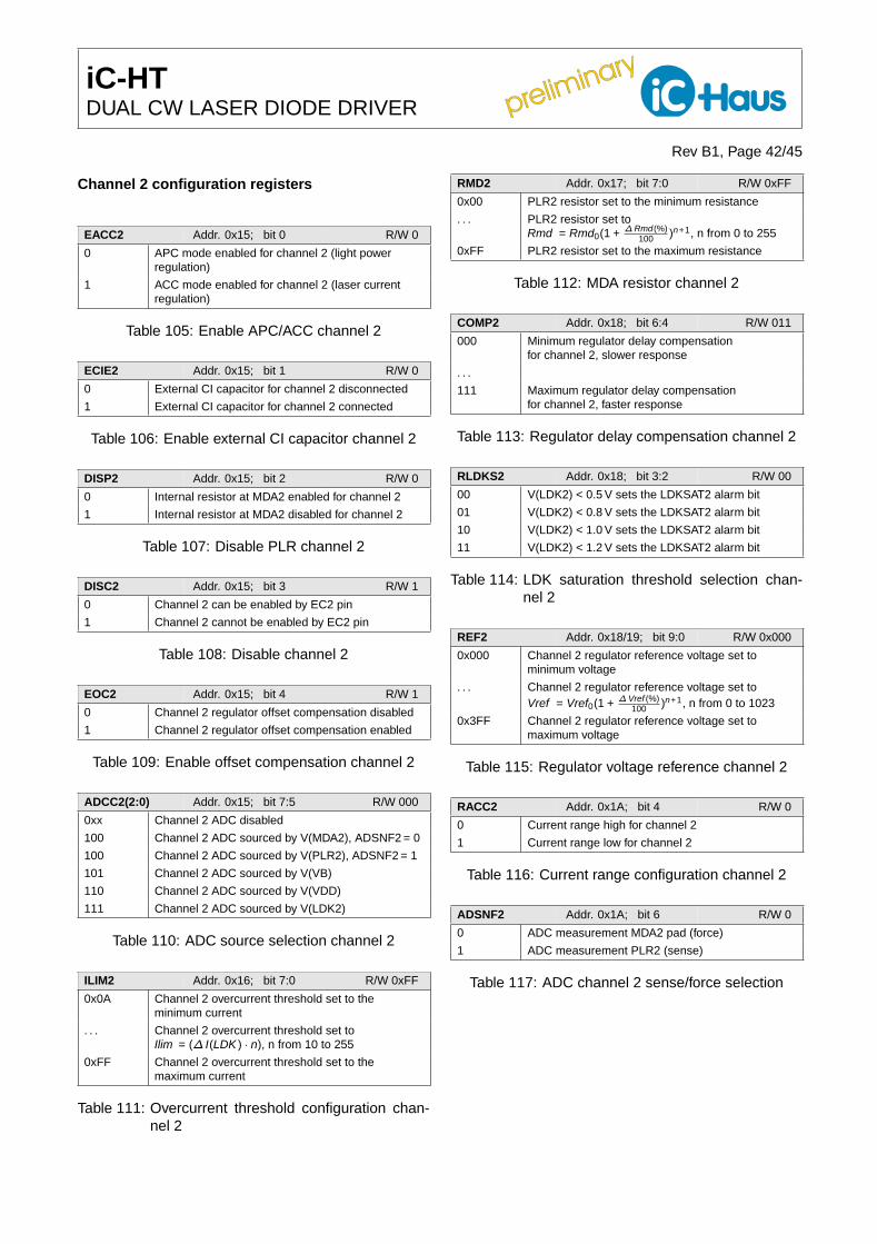
preliminary
preliminary iC-HTDUAL CW LASER DIODE DRIVER
Rev B1, Page 42/45
Channel 2 configuration registers
EACC2 Addr. 0x15; bit 0 R/W 0
0 APC mode enabled for channel 2 (light power
regulation)
1 ACC mode enabled for channel 2 (laser current
regulation)
Table 105: Enable APC/ACC channel 2
ECIE2 Addr. 0x15; bit 1 R/W 0
0 External CI capacitor for channel 2 disconnected
1 External CI capacitor for channel 2 connected
Table 106: Enable external CI capacitor channel 2
DISP2 Addr. 0x15; bit 2 R/W 0
0 Internal resistor at MDA2 enabled for channel 2
1 Internal resistor at MDA2 disabled for channel 2
Table 107: Disable PLR channel 2
DISC2 Addr. 0x15; bit 3 R/W 1
0 Channel 2 can be enabled by EC2 pin
1 Channel 2 cannot be enabled by EC2 pin
Table 108: Disable channel 2
EOC2 Addr. 0x15; bit 4 R/W 1
0 Channel 2 regulator offset compensation disabled
1 Channel 2 regulator offset compensation enabled
Table 109: Enable offset compensation channel 2
ADCC2(2:0) Addr. 0x15; bit 7:5 R/W 000
0xx Channel 2 ADC disabled
100 Channel 2 ADC sourced by V(MDA2), ADSNF2 = 0
100 Channel 2 ADC sourced by V(PLR2), ADSNF2 = 1
101 Channel 2 ADC sourced by V(VB)
110 Channel 2 ADC sourced by V(VDD)
111 Channel 2 ADC sourced by V(LDK2)
Table 110: ADC source selection channel 2
ILIM2 Addr. 0x16; bit 7:0 R/W 0xFF
0x0A Channel 2 overcurrent threshold set to the
minimum current
. . . Channel 2 overcurrent threshold set to
Ilim = (∆ I(LDK ) · n), n from 10 to 255
0xFF Channel 2 overcurrent threshold set to the
maximum current
Table 111: Overcurrent threshold configuration chan-
nel 2
RMD2 Addr. 0x17; bit 7:0 R/W 0xFF
0x00 PLR2 resistor set to the minimum resistance
. . . PLR2 resistor set to
Rmd = Rmd0(1 +∆ Rmd(%)
100)n+1, n from 0 to 255
0xFF PLR2 resistor set to the maximum resistance
Table 112: MDA resistor channel 2
COMP2 Addr. 0x18; bit 6:4 R/W 011
000 Minimum regulator delay compensation
for channel 2, slower response
. . .
111 Maximum regulator delay compensation
for channel 2, faster response
Table 113: Regulator delay compensation channel 2
RLDKS2 Addr. 0x18; bit 3:2 R/W 00
00 V(LDK2) < 0.5 V sets the LDKSAT2 alarm bit
01 V(LDK2) < 0.8 V sets the LDKSAT2 alarm bit
10 V(LDK2) < 1.0 V sets the LDKSAT2 alarm bit
11 V(LDK2) < 1.2 V sets the LDKSAT2 alarm bit
Table 114: LDK saturation threshold selection chan-
nel 2
REF2 Addr. 0x18/19; bit 9:0 R/W 0x000
0x000 Channel 2 regulator reference voltage set to
minimum voltage
. . . Channel 2 regulator reference voltage set to
Vref = Vref0(1 +∆ Vref (%)
100)n+1, n from 0 to 1023
0x3FF Channel 2 regulator reference voltage set to
maximum voltage
Table 115: Regulator voltage reference channel 2
RACC2 Addr. 0x1A; bit 4 R/W 0
0 Current range high for channel 2
1 Current range low for channel 2
Table 116: Current range configuration channel 2
ADSNF2 Addr. 0x1A; bit 6 R/W 0
0 ADC measurement MDA2 pad (force)
1 ADC measurement PLR2 (sense)
Table 117: ADC channel 2 sense/force selection

preliminary
preliminary iC-HTDUAL CW LASER DIODE DRIVER
Rev B1, Page 43/45
General configuration registers
RDCO Addr. 0x1B; bit 5:0 R/W 0x02
0x00 No current
. . .
0x3F 140 µA Typ (see spec point D01)
Table 118: DCO current control
MERGE Addr. 0x1B; bit 6 R/W 0
0 Channel 1 and 2 operate independently
1 Power transistor from channel 2 usable in parallel
with channel 1, regulation made by channel 1.
Table 119: Channel combination
MODE(1:0) Addr. 0x1C; bit 1:0 R/W 01
00 Not allowed, signaled as memory error
01 Chip set in operation mode
(apply configuration, latch transparent)
10 Chip set in configuration mode
(hold previous configuration)
11 Not allowed, signaled as memory error
Table 120: Configuration and operation mode
MOSCERR Addr. 0x1D; bit 0 R/W 0
0 Oscillator error (watchdog) will be signaled at
NCHK
1 Oscillator error (watchdog) will not be signaled at
NCHK
Table 121: Oscillator watchdog error mask
MMONC Addr. 0x1D; bit 1 R/W 1
0 MONC1 and MONC2 event
will be signaled at NCHK
1 MONC1 and MONC2 event
will not be signaled at NCHK
Table 122: Monitor channel 1 and 2 event mask
MLDKSAT1 Addr. 0x1D; bit 2 R/W 1
0 LDKSAT1 event will be signaled at NCHK
1 LDKSAT1 event will not be signaled at NCHK
Table 123: LDK saturation error mask channel 1
MLDKSAT2 Addr. 0x1D; bit 3 R/W 1
0 LDKSAT2 event will be signaled at NCHK
1 LDKSAT2 event will not be signaled at NCHK
Table 124: LDK saturation error mask channel 2
SOVT Addr. 0x1D; bit 4 R/W 0
0 No overtemperature event is simulated.
1 Overtemperature event simulated.
Table 125: Simulate overtemperature
SOVC1 Addr. 0x1D; bit 5 R/W 0
0 No Overcurrent event at channel 1 is simulated.
1 Overcurrent event at channel 1 simulated.
Table 126: Simulate overcurrent channel 1
SOVC2 Addr. 0x1D; bit 6 R/W 0
0 No overcurrent event at channel 2 is simulated.
1 Overcurrent event at channel 2 simulated.
Table 127: Simulate overcurrent channel 2
SOSCERR Addr. 0x1D; bit 7 R/W 0
0 No oscillator error simulated.
1 Oscillator error simulated (watchdog timeout).
Table 128: Simulate oscillator error
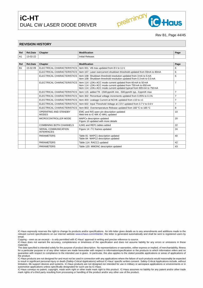
preliminary
preliminary iC-HTDUAL CW LASER DIODE DRIVER
Rev B1, Page 44/45
REVISION HISTORY
Rel Rel.Date Chapter Modification Page
A1 13-02-22 Initial Release.
Rel Rel.Date Chapter Modification Page
B1 15-02-09 ELECTRICAL CHARACTERISTICS Item 001: VB max updated from 8 V to 11 V. 6
ELECTRICAL CHARACTERISTICS Item 107: Laser overcurrent shutdown threshold updated from 93mA to 80mA 6
ELECTRICAL CHARACTERISTICS Item 108: Shutdown threshold resolution updated from 3 mA to 5 mAItem 108: Shutdown threshold resolution updated from 0.3 mA to 0.5 mA
6
ELECTRICAL CHARACTERISTICS Item 114: LDKx ACC mode current updated from 60 mA to 50 mAItem 114: LDKx ACC mode current updated from 750 mA to 650 mAItem 114: LDKx ACC mode current updated typical from 905 mA to 750 mA
7
ELECTRICAL CHARACTERISTICS Item 115: added TK -1500 ppm/K min, -500 ppm/K typ., 0 ppm/K max 7
ELECTRICAL CHARACTERISTICS Item 302: Percentual voltage increments updated from 0.05% to 0.1% 7
ELECTRICAL CHARACTERISTICS Item 403: Leakage Current at NCHK updated from ±10 to ±1 7
ELECTRICAL CHARACTERISTICS Item 602: Input Threshold Voltage at 2.8 V updated from 0.7 V to 0.6 V 7
ELECTRICAL CHARACTERISTICS Item B02: Overtemperature Release updated from 160 °C to 165 °C 8
OPERATING AND STANDBYMODES
EMC and INS open pin description updatedWeb link to iC-WK iC-WKL updated
10
MICROCONTROLLER MODE MAPCx description updatedFigure 10 updated with more details
20
COMBINING BOTH CHANNELS ILIM1 and REF1 tables added 22
SERIAL COMMUNICATIONINTERFACES
Figure 14: I2C frames updated 24
PARAMETERS Table 81: MAPC1 description updatedTable 84: MAPC2 description updated
40
PARAMETERS Table 114: RACC2 updated 42
PARAMETERS Table 120: MMONC description updated 43
iC-Haus expressly reserves the right to change its products and/or specifications. An info letter gives details as to any amendments and additions made to therelevant current specifications on our internet website www.ichaus.com/infoletter; this letter is generated automatically and shall be sent to registered users byemail.Copying – even as an excerpt – is only permitted with iC-Haus’ approval in writing and precise reference to source.iC-Haus does not warrant the accuracy, completeness or timeliness of the specification and does not assume liability for any errors or omissions in thesematerials.The data specified is intended solely for the purpose of product description. No representations or warranties, either express or implied, of merchantability, fitnessfor a particular purpose or of any other nature are made hereunder with respect to information/specification or the products to which information refers and noguarantee with respect to compliance to the intended use is given. In particular, this also applies to the stated possible applications or areas of applications ofthe product.iC-Haus products are not designed for and must not be used in connection with any applications where the failure of such products would reasonably be expectedto result in significant personal injury or death (Safety-Critical Applications) without iC-Haus’ specific written consent. Safety-Critical Applications include, withoutlimitation, life support devices and systems. iC-Haus products are not designed nor intended for use in military or aerospace applications or environments or inautomotive applications unless specifically designated for such use by iC-Haus.iC-Haus conveys no patent, copyright, mask work right or other trade mark right to this product. iC-Haus assumes no liability for any patent and/or other trademark rights of a third party resulting from processing or handling of the product and/or any other use of the product.

preliminary
preliminary iC-HTDUAL CW LASER DIODE DRIVER
Rev B1, Page 45/45
ORDERING INFORMATION
Type Package Order Designation
iC-HT QFN28 5 mm x 5 mm iC-HT QFN28-5x5
Evaluation
Board
100 mm x 80 mm eval board iC-HT EVAL HT1D
For technical support, information about prices and terms of delivery please contact:
iC-Haus GmbH Tel.: +49 (0) 61 35 - 92 92 - 0
Am Kuemmerling 18 Fax: +49 (0) 61 35 - 92 92 - 192
D-55294 Bodenheim Web: http://www.ichaus.com
GERMANY E-Mail: [email protected]
Appointed local distributors: http://www.ichaus.com/sales_partners