i2s audio i/o card - silicon labs · i2s audio i/o card rev. 0.1 3 3. hardware setup refer to...
TRANSCRIPT
Rev. 0.1 7/12 Copyright © 2012 by Silicon Laboratories UPIO-USB-AUDIO
I2S Audio I /O Card
I2S AUDIO I /O CARD USER’S GUIDE
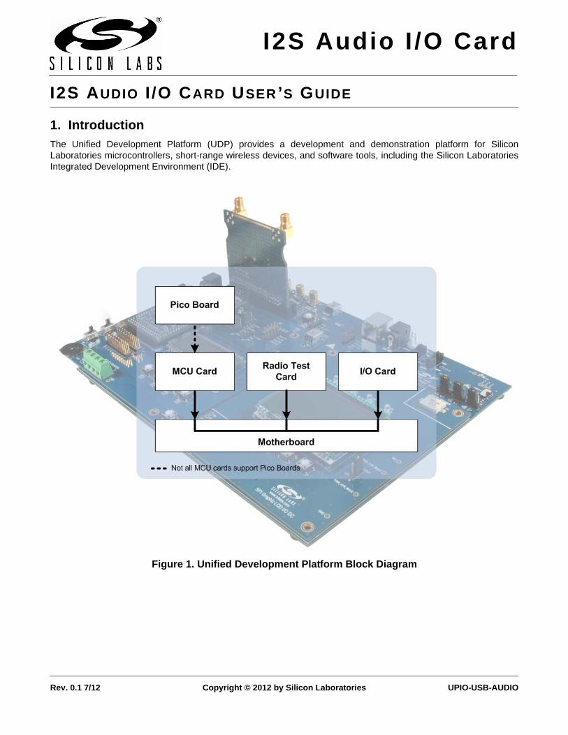
1. IntroductionThe Unified Development Platform (UDP) provides a development and demonstration platform for SiliconLaboratories microcontrollers, short-range wireless devices, and software tools, including the Silicon LaboratoriesIntegrated Development Environment (IDE).
Figure 1. Unified Development Platform Block Diagram

I2S Audio I /O Card
2 Rev. 0.1
2. Relevant Documents
This document provides a hardware overview for the Unified Development Platform (UDP) system USB Audio I/Ocard. Additional information on the UDP system can be found in the documents listed in this section.
2.1. Motherboard User’s GuideThe UDP Motherboard User’s Guide contains information on the motherboard features and can be found atwww.silabs.com/udp.
2.2. Card User’s GuidesThe UDP MCU, I/O, and radio test card User’s Guides can be found at www.silabs.com/udp.
2.3. ExamplesThe Precision32™ Software Development Kit (SDK) includes example firmware using this board. More details onthe use of the board can be found in the example documentation. The SDK can be downloaded from the websiteas part of the Precision32 package at www.silabs.com/32bit-software.
I2S Audio I /O Card
Rev. 0.1 3
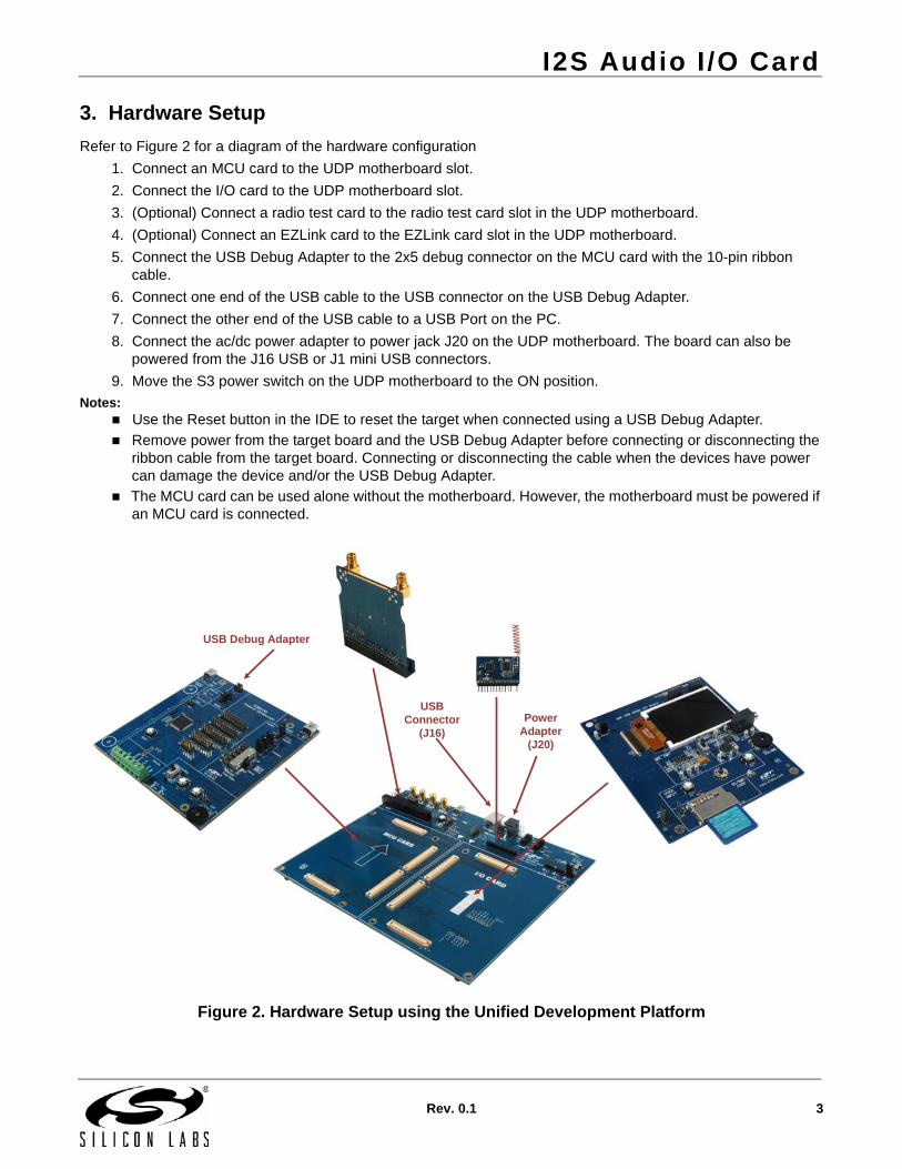
3. Hardware Setup
Refer to Figure 2 for a diagram of the hardware configuration
1. Connect an MCU card to the UDP motherboard slot.
2. Connect the I/O card to the UDP motherboard slot.
3. (Optional) Connect a radio test card to the radio test card slot in the UDP motherboard.
4. (Optional) Connect an EZLink card to the EZLink card slot in the UDP motherboard.
5. Connect the USB Debug Adapter to the 2x5 debug connector on the MCU card with the 10-pin ribbon cable.
6. Connect one end of the USB cable to the USB connector on the USB Debug Adapter.
7. Connect the other end of the USB cable to a USB Port on the PC.
8. Connect the ac/dc power adapter to power jack J20 on the UDP motherboard. The board can also be powered from the J16 USB or J1 mini USB connectors.
9. Move the S3 power switch on the UDP motherboard to the ON position.
Notes:Use the Reset button in the IDE to reset the target when connected using a USB Debug Adapter.
Remove power from the target board and the USB Debug Adapter before connecting or disconnecting the ribbon cable from the target board. Connecting or disconnecting the cable when the devices have power can damage the device and/or the USB Debug Adapter.
The MCU card can be used alone without the motherboard. However, the motherboard must be powered if an MCU card is connected.
Figure 2. Hardware Setup using the Unified Development Platform
USB Debug Adapter
Power Adapter
(J20)
USB Connector
(J16)

I2S Audio I /O Card
4 Rev. 0.1
4. UPIO-USB-AUDIO I/O Card Overview
The USB Audio I/O card adds a microphone, codec, and headphone jack for audio development and an SD cardconnector. The card connects to the I/O Card expansion slot on the UDP motherboard and provides completeaccess to the MCU resources. Each expansion board has a unique ID that can be read out of an EEPROM or MCUon the board, which enables software tools to recognize the connected hardware and automatically select theappropriate firmware image.
Figure 3 shows the USB Audio I/O card.
Figure 3. UPIO-USB-AUDIO I/O Card
Figure 4 and Figure 5 highlight some of the features of the USB Audio I/O card.

I2S Audio I /O Card
Rev. 0.1 5
Figure 4. UPIO-USB-AUDIO I/O Card Features (Front)
Push-ButtonSwitches
LEDs
Headphone Jack
SD Card Connector
Joystick Switch
Graphic QVGA LCD
Potentiometer for Volume Control
Microphone Input Path
Codec

I2S Audio I /O Card
6 Rev. 0.1
Figure 5. UPIO-USB-AUDIO I/O Card Features (Back)
4.1. Microphone InputThe microphone input system on the board consists of two input paths. When SW1 is in the upper position markedwith codec, the microphone connects to the codec (U14). When SW1 is in the lower position, the microphoneconnects to the ADC_IN1 UDP signal through a filter and gain circuit. This filter and gain circuit is biased with theADC_VREF UDP signal.
4.2. Codec (U14) and Headphone Jack (J9)This codec accepts register writes over I2C using the I2C_SDA_EZR and I2C_SCL_EZR signals. TheTIMER_EX_A signal provides the clock, and I2SRX_DOUT_A and I2STX_DOUT_A are the digital audio data inputand output signals. The I2S word sync (WS) and clock (SCK) signals can source from either the I2S receiver or I2Stransmitter on the MCU card. The capacitors, resistors, microphone, and headphone jack connections surroundingthe codec are based on the manufacturer’s recommendations. Table 1 summarizes the codec connections.
Table 1. Codec Connections
Codec Signal UDP SignalCommand I2C data I2C_SDA_EZR
Command I2C clock I2C_SCL_EZR
External clock TIMER_EX_A
I2S word sync (WS) I2STX_DFS_A and I2SRX_DFS_A
I2S clock (SCK) I2STX_CLK_A and I2SRX_CLK_A
I2S input (to codec) data (SD) (DACDAT pin) I2SOUT_DOUT_A
I2S output (from codec) data (SD) (ADCDAT pin) I2SIN_DOUT_A
LCD and Joystick MCUEBID MCU
I2S Audio I /O Card
Rev. 0.1 7
4.3. Potentiometer (R68)The potentiometer connects to the ADC_IN0 signal and can be used for volume control. The MCU card mustimplement firmware to modulate the volume as the potentiometer value changes.
4.4. Switches and LEDsThe I/O card has two push-button switches (S2 and S4) and two LEDs (D1 and D2). The switches are normallyopen and pull the signal voltage to ground when pressed. Table 2 shows the UDP signal connections for theseswitches and LEDs.
4.5. Co-processor MCU (U7)The I/O card has a C8051F380 co-processor MCU (U7) that controls the Graphic QVGA LCD (LCD1) and readsthe five-direction joystick switch (S1). This co-processor enables stand-alone demos that do not require a PC whenconnected with an MCU card through the UDP motherboard.
4.5.1. Graphic QVGA LCD (LCD1)
The graphic QVGA LCD (LCD1) connects to the co-processor C8051F380 MCU EMIF through the J6 connector.This color LCD (SDT022ATFT by Displaytech Ltd.) has a resolution of 320 x 240 resolution. The powerconsumption of the LCD can be measured using the J8 header. Table 3 show the co-processor port pinconnections to the LCD.
Table 2. Switch and LED Connections
SW or LED UDP SignalPush-Button Switch (S4) GPIO00
Push-Button Switch (S2) GPIO01
Blue LED (D2) PWR_3.3_BULK
Red LED (D1) GPIO02
Table 3. Joystick Switch Connections
LCD SignalCo-processor Pin or
UDP SignalIM0 PWR_3.3_BULK
IM3
LEDA
VCC
DB10 P4.0
DB11 P4.1
DB12 P4.2
DB13 P4.3
DB14 P4.4
DB15 P4.5
DB16 P4.6
DB17 P4.7
RD P1.6
RS/SCL P3.0
WR P1.7
LCD_RESET P1.1

I2S Audio I /O Card
8 Rev. 0.1
4.5.2. Joystick Switch
The I/O card has a five-position joystick switch (S1) that connects to the co-processor C8051F380 MCU. Thejoystick is normally open and pulls a signal voltage to ground when the joystick is placed in one of the fivepositions. Table 4 show the co-processor port pin connections to the joystick.
4.6. SD Card Connector (U10)The SD card connector (U10) connects to any standard SD card. The card power from PWR_3.3_BULK can beenabled or disabled by the SPI_PWR signal connected to GPIO03.
The connector includes two mechanical switches: one detects if a card is inserted, and one indicates the writeprotection status of the card. The card detection switch connects to the GPIO04 signal. The JP3 header providesaccess to both the switch signals.
4.7. EBID MCU (U11)The I/O card has a unique ID that can be read out from the Silicon Labs C8051F990 MCU (U11). This MCUenables software tools to recognize the connected hardware and automatically select the appropriate firmwareimage.
Table 4. Joystick Switch Connections
Joystick Position Co-processor PinCenter P0.6
Up P0.2
Down P0.3
Left P0.4
Right P0.5

I2S Audio I /O Card
Rev. 0.1 9
5. Using the I/O Card with the UDP Motherboard
5.1. Current MeasurementThe power measurement circuitry on the UDP motherboard consists of a Silicon Labs C8051F351 8051 MCU thatmeasures both input voltage and current consumption of the MCU card, I/O expander, and radio test card. Whenusing the I/O card, install a shorting block on the UDP Motherboard J15 and J13 connecting the two left pinstogether.
Figure 6. Power Measurement Diagram
5.2. I/O Card Header ConnectionsThe I/O card has four connectors with 100 pins each. These 400 pins are directly tied to the UDP motherboard andMCU cards. These signals are named and designed to support a wide variety of features and applications, and theUPIO-USB-AUDIO card implements a subset of these connections.
The MCU cards and I/O cards are designed so that a maximum number of functions are shared between eachcard. This allows a particular type of I/O card to be shared amongst all MCU cards that connect to the samesignals.
The I/O card slot includes the following components:
H1 I/O card connector H1H2 I/O card connector H2H3 I/O card connector H3H4 I/O card connector H4
The UPIO-USB-AUDIO card implements the signals described in Table 6, Table 7, and Table 8, Table 9 in theAppendix.
UDP motherboard power
to VIOpower
VIO IN power
to Radio card power
Radio card IN power
to VDDpower
VDD IN powerJ15 J14 J13
C8051F351
JP3 JP2 JP1R24 R15 R6

I2S Audio I /O Card
10 Rev. 0.1
5.3. Shorting Blocks: Factory DefaultsThe UPIO-USB-AUDIO I/O Card has a factory pre-installed shorting blocks on JP4, JP3, and J8. Figure 7 showsthe position of the factory default shorting blocks.
Figure 7. Shorting Blocks: Factory Defaults

I2S Audio I /O Card
Rev. 0.1 11
6. Schematics5 5
4 4
3 3
2 2
1 1
D C B A
Tied to Gnd with 0 Ohm Resistor
(in AUDIO_PATH)
HEADPHONE JACK
MIC AMP
AUDIO CODEC
A_G
ND
A_G
ND
PWR
_3.3
_BU
LK
A_G
ND
PWR
_3.3
_BU
LK
A_G
ND
A_G
ND
A_G
ND
PWR
_3.3
_BU
LKPW
R_5
.0_B
ULK
PWR
_5.0
_BU
LK
PWR
_3.3
_BU
LK
PWR
_3.3
_BU
LKPW
R_3
.3_B
ULK
A_G
ND
A_G
ND
A_G
ND
A_G
ND
A_G
ND
A_G
ND
A_G
ND
A_G
ND
I2ST
X_W
S_A
I2SR
X_W
S_A
I2ST
X_SC
K_A
I2SR
X_SC
K_A
I2SR
X_SD
_A
TIM
ER_E
X_A
I2ST
X_SD
_AI2
C_S
DA_
EZR
VMID
HP_
RIG
HT
I2C
_SC
L_EZ
R
HP_
LEFT
HP_
LEFT
HP_
RIG
HT
VMID
MIC
-
ADC
_VR
EF
ADC
_IN
1
MIC
+
MIC
-
MIC
+
Title
Size
Doc
umen
t Num
ber
Rev
Dat
e:Sh
eet
of
400
W C
esar
Cha
vez
Aust
in, T
X 7
8701
UPI
O-U
SB-A
UD
IO1.
0
I2S
AUD
IO I/
O C
ARD
- AU
DIO
PAT
H
B
15
Frid
ay, M
ay 0
4, 2
012
Title
Size
Doc
umen
t Num
ber
Rev
Dat
e:Sh
eet
of
400
W C
esar
Cha
vez
Aust
in, T
X 7
8701
UPI
O-U
SB-A
UD
IO1.
0
I2S
AUD
IO I/
O C
ARD
- AU
DIO
PAT
H
B
15
Frid
ay, M
ay 0
4, 2
012
Title
Size
Doc
umen
t Num
ber
Rev
Dat
e:Sh
eet
of
400
W C
esar
Cha
vez
Aust
in, T
X 7
8701
UPI
O-U
SB-A
UD
IO1.
0
I2S
AUD
IO I/
O C
ARD
- AU
DIO
PAT
H
B
15
Frid
ay, M
ay 0
4, 2
012
C62
0.1u
F
C58
0.1u
F
C46
1uF
+ -
V+ V-
U15
AM
C33
204
3 21
114
R60
4.99
K
C40
1uF
R66
100K
C54
0.1u
F
R43
1.5k
TP3
HP_
LEFT
R40
0
C36
0.1u
F
C59
1uF
+
-
U15
CM
C33
204
10
98
TP12
MIC
+
WM
8976
U14 LI
P1
LIN
2
L2/G
PIO
23
DN
C4
DN
C5
DN
C6
LRC
7
BCLK
8S
DIN
17M
OD
E18
AUXL
19AU
XR20
OU
T421
OU
T322
RO
UT2
23S
PK
GN
D24
LOUT225
VMID27 AGND28 ROUT129 LOUT130 AVDD31 MICBIAS32
ADCDAT9
DACDAT10
MCLK11
GND12
DCVDD13
DBVDD14
CSB/GPIO115
SCLK16
EPAD33
SPKVDD26
R61
154K
C43
0.1u
F
C47
10uF
MK2
MIC
RO
PHO
NE
1 2
R44
1.5k
TP13
LP1
+
-
U15
DM
C33
204
12
1314
TP11
MIC
-
R63
4.99
K
C61
2700
pF
C41
0.1u
F
TP4
HP_
RIG
HT
C55
6.8p
F
R41
4.7K
R67
0N
I
JP4
VAM
P Im
easu
re
C37
0.1u
F
C48
10uF
R56
2K
TP14
LP2
R64
133K
C44
0.1u
F
+C
5610
uF
R57
100K
C42
0.1u
F
TP2
SPK_
NEG
R42
681
R65
9.76
K
C33
0.1u
F
SW1
SW_S
LID
E_2P
OS1 2 3
R45
0
C57
0.1u
F
+ -
U15
B
MC
3320
45 6
7
R58
5.1M
C45
1uF
JS3
Jum
per S
hunt
C60
1uF
J9AU
DIO
JAC
K
1342
R62
4.22
K
TP1
SPK_
POS
R59
154K
C34
220p
F
C35
0.1u
F
C39
1uF
C53
8.2n
F
Fig
ure
8.U
PIO
-US
B-A
UD
IO I/
O C
ard
Sch
emat
ic (
1 o
f 5)

I2S Audio I /O Card
12 Rev. 0.1
5 5
4 4
3 3
2 2
1 1
D C B A
Ground Access
User Input
User Feedback
SD/MMC Card
Electronic Board Identification (EBID)
PWR
_3.3
_BU
LK
PWR
_3.3
_BU
LK
PWR
_3.3
_BU
LK
PWR
_3.3
_BU
LKPW
R_3
.3_B
ULK
PWR
_3.3
_BU
LK
A_G
ND
PWR
_SYS
_BU
LK
PWR
_SYS
_BU
LK
UD
PBU
S_SC
L_A
UD
PBU
S_SD
A_A
C2_
DAT
_DC
2_C
LK_D
C2_
CLK
_D
C2_
DAT
_D
GPI
O01
ADC
_IN
0
GPI
O02
GPI
O00
SD_S
W
SPI_
NSS
0_EZ
RSP
I_M
OSI
_EZR
SPI_
SCK_
EZR
SPI_
MIS
O_E
ZRSP
I_PW
R
Title
Size
Doc
umen
t Num
ber
Rev
Dat
e:Sh
eet
of
400
W C
esar
Cha
vez
Aust
in, T
X 7
8701
UPI
O-U
SB-A
UD
IO1.
0
I2S
AUD
IO I/
O C
ARD
- I/O
B
25
Frid
ay, M
ay 0
4, 2
012
Title
Size
Doc
umen
t Num
ber
Rev
Dat
e:Sh
eet
of
400
W C
esar
Cha
vez
Aust
in, T
X 7
8701
UPI
O-U
SB-A
UD
IO1.
0
I2S
AUD
IO I/
O C
ARD
- I/O
B
25
Frid
ay, M
ay 0
4, 2
012
Title
Size
Doc
umen
t Num
ber
Rev
Dat
e:Sh
eet
of
400
W C
esar
Cha
vez
Aust
in, T
X 7
8701
UPI
O-U
SB-A
UD
IO1.
0
I2S
AUD
IO I/
O C
ARD
- I/O
B
25
Frid
ay, M
ay 0
4, 2
012
R55
1K
R50
4.7K
TP9 G
ND
BLU
E
R54
0N
I
R51
330
JS2
Jum
per S
hunt
TP10 A_
GN
D
BLU
EU
10 SD/M
MC
CAR
D
DAT
3/C
S1
CM
D/M
OSI
2
GND3
VDD
4
CLK
/SC
LK5
GND6
DA
T0/M
ISO
7
DAT
18
DAT
29
SW
10
WP
11
CASE12
CASE13
C49
0.1u
F
JP2
CO
NN
SO
CKE
T 4X
1
JP3
JUM
PER
S4G
PIO
0
R69
100
R47
100K
R68
10K
13
2
U11
C80
51F9
90
P0.
1_A
GN
D1
GND3
VDD4
RST
_C2C
K5
P2.
7_C
2D6
P1.
77
P1.
68
P0.
220
P1.
1_C
PO
-13
P1.
0_C
PO
+14
P1.
310
P1.
59
P1.
211
P0.
319
P0.
7_IR
EF
15P
0.6_
CO
NV
VS
TR16
P0.
0_V
RE
F2
RX_
P0.
517
TX_P
0.4
18
GNDEPADGND
12
D1
RED
GPI
O2
D2
Blue
R48
4.7K
C50
0.1u
F
C51
1uF
U9
SN74
LVC
1G66
DC
K
IN1
OU
T2
GND3
C4
VCC5
R53
0N
I
R49
100K
C52
0.1u
F
TP8 G
ND
BLU
E
S2G
PIO
1
Fig
ure
9.U
PIO
-US
B-A
UD
IO I/
O C
ard
Sch
emat
ic (
2 o
f 5)

I2S Audio I /O Card
Rev. 0.1 13
PW
R_3
.3_B
ULK
PW
R_3
.3_B
ULK
PW
R_3
.3_B
ULK
PW
R_S
YS
_BU
LK
PW
R_3
.3_B
ULK
PW
R_3
.3_B
ULK
PW
R_S
YS
_BU
LK
EM
IF_D
7
EM
IF_D
6
EM
IF_D
5
EM
IF_D
4
EM
IF_D
3
EM
IF_D
2
EM
IF_D
1
EM
IF_D
0
LCD
_RE
SE
T
SW
_U SW
_C
SW
_L
C2_
DA
T_E
C2_
CLK
_E
SW
_CLCD
_RE
SE
T
SW
_RS
W_L
SW
_DS
W_U
UD
PB
US
_SC
L_A
UD
PB
US
_SD
A_A
C2_
CLK
_E
C2_
DA
T_E
EM
IF_O
EB
EM
IF_W
RB
EM
IF_A
0
EM
IF_D
0
EM
IF_D
1
EM
IF_D
2
EM
IF_D
3
EM
IF_D
4
EM
IF_D
5
EM
IF_D
6
EM
IF_D
7
SW
_R SW
_D
EM
IF_A
0
EM
IF_O
EB
EM
IF_W
RB
Title
Siz
eD
ocum
ent N
umbe
rR
ev
Dat
e:S
heet
of
400
W C
esar
Cha
vez
Aus
tin, T
X 7
8701
UP
IO-U
SB
-AU
DIO
1.0
I2S
AU
DIO
I/O
CA
RD
- D
EM
O S
UP
PO
RT
B
35
Frid
ay, M
ay 0
4, 2
012
Title
Siz
eD
ocum
ent N
umbe
rR
ev
Dat
e:S
heet
of
400
W C
esar
Cha
vez
Aus
tin, T
X 7
8701
UP
IO-U
SB
-AU
DIO
1.0
I2S
AU
DIO
I/O
CA
RD
- D
EM
O S
UP
PO
RT
B
35
Frid
ay, M
ay 0
4, 2
012
Title
Siz
eD
ocum
ent N
umbe
rR
ev
Dat
e:S
heet
of
400
W C
esar
Cha
vez
Aus
tin, T
X 7
8701
UP
IO-U
SB
-AU
DIO
1.0
I2S
AU
DIO
I/O
CA
RD
- D
EM
O S
UP
PO
RT
B
35
Frid
ay, M
ay 0
4, 2
012
CTR
S1
JOY
STI
CK
EV
Q-Q
7GA
50
A1
E2
B3
COM4
D5
CO
M6
C7
COM8
GND9
GND10
JP1
CO
NN
SO
CK
ET
4X1
R38
100K
R39
4.75
K
R26
100K
C4
0.1u
F
R33
4.75
K
JS1
Jum
per
Shu
nt
C5
0.1u
F
R27
100K
LCD
1LC
D M
OD
ULE
C19
0.1u
F
R28
4.75
K
R35
100K
C32
1uF
R30
100K
C20
4.7u
F
R36
4.75
K
U7
C80
51F3
80
P0.
51
P0.
42
P0.
33
P0.
24
P0.
15
P0.
06
GN
D7
D+
8
D-
9
VD
D10
RE
GIN
11
VB
US
12
RST/C2CK13
C2D14
P4.715
P4.616
P4.517
P4.418
P4.319
P4.220
P4.121
P4.022
P3.723
P3.624
P3.
525
P3.
426
P3.
327
P3.
228
P3.
129
P3.
030
P2.
731
P2.
632
P2.
533
P2.
434
P2.
335
P2.
236
P2.137 P2.038 P1.739 P1.640 P1.541 P1.442 P1.343 P1.244 P1.145 P1.046 P0.747 P.0648
J6 FH19
SC
-45S
-0.5
SH
(05)
NC
1
IM0
2
IM1
3
IM2
4
IM3
5
RE
SE
T6
VS
YN
C7
HS
YN
C8
DO
TCLK
9
EN
AB
LE10
DB
1711
DB
1612
DB
1513
DB
1414
DB
1315
DB
1216
DB
1117
DB
1018
DB
919
DB
820
DB
721
DB
622
DB
523
DB
424
DB
325
DB
226
DB
127
DB
028
SD
O29
SD
I30
RD
31R
S/S
CL
32W
R33
CS
34FM
AR
K35
VC
C36
GN
D37
LED
A38
LED
K1
39LE
DK
240
LED
K3
41Y
D(N
C)
42X
R(N
C)
43Y
U(N
C)
44X
L(N
C)
45
C16
0.1u
F
J8 JUM
PE
RIm
easu
re
R16
1K
C17
0.1u
F
C18
0.1u
FR
704.
75K
Fig
ure
10.U
PIO
-US
B-A
UD
IO I/
O C
ard
Sch
emat
ic (
3 o
f 5)

I2S Audio I /O Card
14 Rev. 0.1
SD_S
WSP
I_PW
RG
PIO
02G
PIO
01G
PIO
00
I2SR
X_SD
_AI2
SRX_
SCK_
AI2
SRX_
WS_
A
SPI_
NSS
0_EZ
RSP
I_M
OSI
_EZR
SPI_
MIS
O_E
ZRSP
I_SC
K_EZ
R
TIM
ER_E
X_A
I2C
_SC
L_EZ
RI2
C_S
DA_
EZR
I2ST
X_SD
_AI2
STX_
SCK_
AI2
STX_
WS_
A
UD
PBU
S_SC
L_A
UD
PBU
S_SD
A_A
Title
Size
Doc
umen
t Num
ber
Dat
e:Sh
eet
400
W C
esar
Cha
vez
Aust
in, T
X 7
8701
UPI
O-U
SB-A
UD
IO
I2S
AUD
IO I/
O C
ARD
- U
DP1
B
Frid
ay,M
ay04
,201
2
Title
Size
Doc
umen
t Num
ber
Dat
e:Sh
eet
400
W C
esar
Cha
vez
Aust
in, T
X 7
8701
UPI
O-U
SB-A
UD
IO
I2S
AUD
IO I/
O C
ARD
- U
DP1
B
Frid
ay,M
ay04
,201
2
Title
Size
Doc
umen
t Num
ber
Dat
e:Sh
eet
400
W C
esar
Cha
vez
Aust
in, T
X 7
8701
UPI
O-U
SB-A
UD
IO
I2S
AUD
IO I/
O C
ARD
- U
DP1
B
Frid
ay,M
ay04
,201
2
H1
CO
NN
_UD
P_IO
_H1
GN
D51
UAR
T_TX
_SYS
52
UAR
T_C
TS_A
53
UAR
T_R
TS_A
54
UAR
T_R
X_A
55
UAR
T_TX
_A56
TIM
ER
_EX_
B57
TIM
ER
_CT_
B58
TIM
ER
_EX_
A59
TIM
ER
_CT_
A60
I2C
_SC
L_E
ZR61
I2C
_SD
A_E
ZR62
I2SO
UT_
DO
UT_
A63
I2S
OU
T_C
LK_A
64
I2S
OU
T_D
FS_A
65
PCA_
CH
1_B
66
PCA_
CH
0_B
67
PC
A_E
CI_
B68
PCA_
CH
1_A
69
PCA_
CH
0_A
70
PC
A_E
CI_
A71
LIN
_RX_
A72
LIN
_TX_
A73
EPC
A_C
H5_
A74
EPC
A_C
H4_
A75
EPC
A_C
H3_
A76
EPC
A_C
H2_
A77
EPC
A_C
H1_
A78
EPC
A_C
H0_
A79
EP
CA
_EC
I_A
80
USA
RT_
UC
LK_B
81
USA
RT_
CTS
_B82
USA
RT_
RTS
_B83
USA
RT_
RX_
B84
US
AR
T_TX
_B85
SP
I_N
SS
3_A
86
SP
I_N
SS
2_A
87
SP
I_N
SS
1_A
88
SP
I_N
SS
0_A
89
SP
I_M
OS
I_A
90
SP
I_M
ISO
_A91
SP
I_S
CK
_A92
CAN
_RX_
B93
CAN
_TX_
B94
USA
RT_
UC
LK_A
95
USA
RT_
CTS
_A96
USA
RT_
RTS
_A97
USA
RT_
RX_
A98
US
AR
T_TX
_A99
GN
D10
0
LPTI
ME
R_O
UT_
A1
LPTI
ME
R_I
N_A
2
LIN
_RX_
B3
LIN
_TX_
B4
CAN
_RX_
A5
CAN
_TX_
A6
EXT
_DM
A_T
RIG
17
EXT
_DM
A_T
RIG
08
EXT_
DAC
_TR
IG1
9
EXT_
DAC
_TR
IG0
10
EXT
_AD
C_T
RIG
111
EXT
_AD
C_T
RIG
012
EXT
_IN
T113
EXT
_IN
T014
WA
KE
UP
115
WA
KE
UP
016
POR
T_M
ATC
H1
17
POR
T_M
ATC
H0
18
GP
IO15
19
GP
IO14
20
GP
IO13
21
GP
IO12
22
GP
IO11
23
GP
IO10
24
GP
IO09
25
GP
IO08
26
GP
IO07
27
GP
IO06
28
GP
IO05
29
GP
IO04
30
GP
IO03
31
GP
IO02
32
GP
IO01
33
GP
IO00
34
CLK
OU
T035
I2SI
N_D
OU
T_A
36
I2SI
N_C
LK_A
37
I2SI
N_D
FS_A
38
I2C
_SC
L_B
39
I2C
_SD
A_B
40
SP
I_N
SS
3_E
ZR41
SP
I_N
SS
2_E
ZR42
SP
I_N
SS
1_E
ZR43
SP
I_N
SS
0_E
ZR44
SP
I_M
OS
I_E
ZR45
SP
I_M
ISO
_EZR
46
SP
I_S
CK
_EZR
47
UAR
T_C
TS_S
YS48
UAR
T_R
TS_S
YS49
UAR
T_R
X_SY
S50
H2
CO
NN
_UD
P_IO
_H2
GN
D51
EM
IF_B
E0B
52
EM
IF_C
S1B
53
EM
IF_B
E1B
54
EM
IF_C
S0B
55
EM
IF_A
LE56
EM
IF_O
EB
57
EM
IF_W
RB
58
EM
IF_A
059
EM
IF_A
160
EM
IF_A
261
EM
IF_A
362
EM
IF_A
463
EM
IF_A
564
EM
IF_A
665
EM
IF_A
766
EM
IF_A
867
EM
IF_A
968
EM
IF_A
1069
EM
IF_A
1170
EM
IF_A
1271
EM
IF_A
1372
EM
IF_A
1473
EM
IF_A
1574
EM
IF_A
1675
EM
IF_A
1776
EM
IF_A
1877
EM
IF_A
1978
EM
IF_A
2079
EM
IF_A
2180
EM
IF_A
2281
EM
IF_A
2382
HVG
PIO
783
HVG
PIO
684
HVG
PIO
585
HVG
PIO
486
HVG
PIO
387
HVG
PIO
288
HVG
PIO
189
HVG
PIO
090
EPC
A_C
H5_
MO
TOR
91
EPC
A_C
H4_
MO
TOR
92
EPC
A_C
H3_
MO
TOR
93
EPC
A_C
H2_
MO
TOR
94
EPC
A_C
H1_
MO
TOR
95
EPC
A_C
H0_
MO
TOR
96
EP
CA
_EC
I_M
OTO
R97
UD
PBU
S_SC
L_A
98
UD
PB
US
_SD
A_A
99
GN
D10
0
CM
OS
CLK
_XTA
L2_A
1
CM
OS
CLK
_XTA
L1_A
2
LCD
_CO
M7_
A3
LCD
_CO
M6_
A4
LCD
_CO
M5_
A5
LCD
_CO
M4_
A6
LCD
_CO
M3_
A7
LCD
_CO
M2_
A8
LCD
_CO
M1_
A9
LCD
_CO
M0_
A10
LCD
_SE
G39
_A11
LCD
_SE
G38
_A12
LCD
_SE
G37
_A13
LCD
_SE
G36
_A14
LCD
_SE
G35
_A15
LCD
_SE
G34
_A16
LCD
_SE
G33
_A17
LCD
_SE
G32
_A18
LCD
_SE
G31
_A19
LCD
_SE
G30
_A20
LCD
_SE
G29
_A21
LCD
_SE
G28
_A22
LCD
_SE
G27
_A23
LCD
_SE
G26
_A24
LCD
_SE
G25
_A25
LCD
_SE
G24
_A26
LCD
_SE
G23
_A27
LCD
_SE
G22
_A28
LCD
_SE
G21
_A29
LCD
_SE
G20
_A30
LCD
_SE
G19
_A31
LCD
_SE
G18
_A32
LCD
_SE
G17
_A33
LCD
_SE
G16
_A34
LCD
_SE
G15
_A35
LCD
_SE
G14
_A36
LCD
_SE
G13
_A37
LCD
_SE
G12
_A38
LCD
_SE
G11
_A39
LCD
_SE
G10
_A40
LCD
_SE
G09
_A41
LCD
_SE
G08
_A42
LCD
_SE
G07
_A43
LCD
_SE
G06
_A44
LCD
_SE
G05
_A45
LCD
_SE
G04
_A46
LCD
_SE
G03
_A47
LCD
_SE
G02
_A48
LCD
_SE
G01
_A49
LCD
_SE
G00
_A50
Fig
ure
11.U
PIO
-US
B-A
UD
IO I/
O C
ard
Sch
emat
ic (
4 o
f 5)

I2S Audio I /O Card
Rev. 0.1 15
54
32
PWR
_3.3
_BU
LK
PWR
_5.0
_BU
LK
PWR
_SYS
_BU
LK
C2_
DAT
_EC
2_C
LK_E
C2_
DAT
_DC
2_C
LK_D
ADC
_IN
1AD
C_I
N0
ADC
_VR
EF
Title
400
W C
esar
Cha
vez
Aust
in, T
X 7
8701
Title
400
W C
esar
Cha
vez
Aust
in, T
X 7
8701
Title
400
W C
esar
Cha
vez
Aust
in, T
X 7
8701
H3
CO
NN
_UD
P_IO
_H3
GN
D51
NC
52
C2_
DAT
_E53
C2_
CLK
_E54
C2_
DAT
_D55
C2_
CLK
_D56
C2_
DAT
_C57
C2_
CLK
_C58
C2_
DAT
_B59
C2_
CLK
_B60
C2_
DAT
_A61
C2_
CLK
_A62
EBID
_NSS
63
EB
ID_M
ISO
64
EB
ID_M
OS
I65
EBID
_SC
K66
GN
D67
PW
R_S
YS_B
ULK
68
PW
R_S
YS_B
ULK
69
PW
R_3
.3V
_BU
LK70
PW
R_3
.3V
_BU
LK71
PW
R_3
.3V
_BU
LK72
PW
R_3
.3V
_BU
LK73
PW
R_5
.0V
_BU
LK74
PW
R_5
.0V
_BU
LK75
PW
R_5
.0V
_BU
LK76
PW
R_5
.0V
_BU
LK77
PW
R_V
PP
_BU
LK78
PW
R_V
PP
_BU
LK79
PWR
_HV2
_BU
S80
PWR
_HV2
_BU
S81
PWR
_HV1
_BU
S82
PWR
_HV1
_BU
S83
PWR
_AU
X_BU
S84
PWR
_AU
X_BU
S85
PWR
_IO
_BU
S86
PWR
_IO
_BU
S87
PWR
_IO
_OU
T88
PWR
_IO
_OU
T89
PWR
_IO
_IN
90
PWR
_IO
_IN
91
PWR
_RAD
IO_O
UT
92
PWR
_RAD
IO_O
UT
93
PWR
_RAD
IO_I
N94
PWR
_RAD
IO_I
N95
PWR
_VD
D_O
UT
96
PWR
_VD
D_O
UT
97
PWR
_VD
D_I
N98
PWR
_VD
D_I
N99
GN
D10
0
NC
1
NC
2
NC
3
NC
4
NC
5
NC
6
NC
7
NC
8
NC
9
NC
10
NC
11
NC
12
NC
13
NC
14
NC
15
NC
16
NC
17
NC
18
NC
19
NC
20
NC
21
NC
22
NC
23
NC
24
NC
25
NC
26
NC
27
NC
28
NC
29
NC
30
NC
31
NC
32
NC
33
NC
34
NC
35
NC
36
NC
37
NC
38
NC
39
NC
40
NC
41
NC
42
NC
43
NC
44
NC
45
NC
46
NC
47
NC
48
JTA
G_T
DI_
A49
JTA
G_T
DO
_A50
H4
CO
NN
_UD
P_IO
_H4
IDAC
_B51
IDAC
_A52
GN
D53
DAC
_OU
T354
DAC
_OU
T255
DAC
_OU
T156
DAC
_OU
T057
DAC
_VR
EFG
ND
58
DAC
_VR
EF59
GN
D60
ADC
_IN
361
ADC
_IN
262
ADC
_IN
163
ADC
_IN
064
AD
C_V
RE
FGN
D65
ADC
_VR
EF66
GN
D67
C2D
_RX1
5_A
68
C2D
_RX1
4_A
69
C2D
_RX1
3_A
70
C2D
_RX1
2_A
71
C2D
_RX1
1_A
72
C2D
_RX1
0_A
73
C2D
_RX0
9_A
74
C2D
_RX0
8_A
75
C2D
_RX0
7_A
76
C2D
_RX0
6_A
77
C2D
_RX0
5_A
78
C2D
_RX0
4_A
79
C2D
_RX0
3_A
80
C2D
_RX0
2_A
81
C2D
_RX0
1_A
82
C2D
_RX0
0_A
83
C2D
_TX1
5_A
84
C2D
_TX1
4_A
85
C2D
_TX1
3_A
86
C2D
_TX1
2_A
87
C2D
_TX1
1_A
88
C2D
_TX1
0_A
89
C2D
_TX0
9_A
90
C2D
_TX0
8_A
91
C2D
_TX0
7_A
92
C2D
_TX0
6_A
93
C2D
_TX0
5_A
94
C2D
_TX0
4_A
95
C2D
_TX0
3_A
96
C2D
_TX0
2_A
97
C2D
_TX0
1_A
98
C2D
_TX0
0_A
99
GN
D10
0
GN
D1
NC
2
NC
3
NC
4
ITM
_CLK
5
ITM
_DA
T36
ITM
_DA
T27
ITM
_DA
T18
ITM
_DA
T09
NC
10
EZR
_GP
IO4
11
EZR
_GP
IO3
12
EZR
_GP
IO2
13
EZR
_GP
IO1
14
EZR
_GP
IO0
15
EZR
_VD
I16
EZR
_AR
SS
I17
EZR
_RE
SE
T18
EZR
_SI1
00X_
RX
19
EZR
_EFI
T20
EZR
_DTO
21
EZR
_SI1
00X_
TX22
EZR
_NFF
S23
EZR
P_N
IRQ
24
EZR
P_S
DN
25
GN
D26
EZR
P_R
X_D
ATA
_OU
T27
EZR
P_R
X_C
LK_O
UT
28
EZR
P_T
X_D
ATA
_IN
29
GN
D30
EZR
P_C
LK_I
N31
GN
D32
EXT
RE
G_B
D_A
33
EXT
RE
G_O
UT_
A34
EXT
RE
G_S
N_A
35
EXT
RE
G_S
P_A
36
I2V_
INN
_A37
I2V
_IN
P_A
38
GN
D39
HVD
A_IN
N_B
40
HVD
A_IN
P_B
41
HVD
A_IN
N_A
42
HVD
A_IN
P_A
43
GN
D44
CP_
NEG
_B45
CP
_PO
S_B
46
CP_
NEG
_A47
CP
_PO
S_A
48
CP_
OU
TA_A
49
CP_
OU
T_A
50
Fig
ure
12.U
PIO
-US
B-A
UD
IO I/
O C
ard
Sch
emat
ic (
5 o
f 5)
I2S Audio I /O Card
16 Rev. 0.1
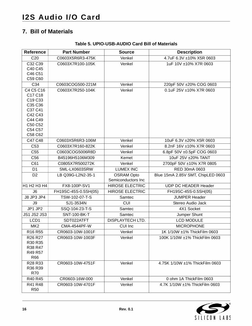
7. Bill of Materials
Table 5. UPIO-USB-AUDIO Card Bill of Materials
Reference Part Number Source DescriptionC20 C0603X5R6R3-475K Venkel 4.7uF 6.3V ±10% X5R 0603
C32 C39 C40 C45 C46 C51 C59 C60
C0603X7R100-105K Venkel 1uF 10V ±10% X7R 0603
C34 C0603COG500-221M Venkel 220pF 50V ±20% COG 0603
C4 C5 C16 C17 C18 C19 C33 C35 C36 C37 C41 C42 C43 C44 C49 C50 C52 C54 C57 C58 C62
C0603X7R250-104K Venkel 0.1uF 25V ±10% X7R 0603
C47 C48 C0603X5R6R3-106M Venkel 10uF 6.3V ±20% X5R 0603
C53 C0603X7R160-822K Venkel 8.2nF 16V ±10% X7R 0603
C55 C0603COG5006R8D Venkel 6.8pF 50V ±0.5pF COG 0603
C56 B45196H5106M309 Kemet 10uF 25V ±20% TANT
C61 C0805X7R500272K Venkel 2700pF 50V ±10% X7R 0805
D1 SML-LX0603SRW LUMEX INC RED 30mA 0603
D2 LB Q39G-L2N2-35-1 OSRAM OptoSemiconductors Inc
Blue 15mA 2.85V SMT, ChipLED 0603
H1 H2 H3 H4 FX8-100P-SV1 HIROSE ELECTRIC UDP DC HEADER Header
J6 FH19SC-45S-0.5SH(05) HIROSE ELECTRIC FH19SC-45S-0.5SH(05)
J8 JP3 JP4 TSW-102-07-T-S Samtec JUMPER Header
J9 SJ1-3534N CUI Stereo Audio Jack
JP1 JP2 SSQ-104-23-T-S Samtec 4X1 Socket
JS1 JS2 JS3 SNT-100-BK-T Samtec Jumper Shunt
LCD1 SDT022ATFT DISPLAYTECH LTD. LCD MODULE
MK2 CMA-4544PF-W CUI Inc MICROPHONE
R16 R55 CR0603-10W-1001F Venkel 1K 1/10W ±1% ThickFilm 0603
R26 R27 R30 R35 R38 R47 R49 R57
R66
CR0603-10W-1003F Venkel 100K 1/10W ±1% ThickFilm 0603
R28 R33 R36 R39
R70
CR0603-10W-4751F Venkel 4.75K 1/10W ±1% ThickFilm 0603
R40 R45 CR0603-16W-000 Venkel 0 ohm 1A ThickFilm 0603
R41 R48 R50
CR0603-10W-4701F Venkel 4.7K 1/10W ±1% ThickFilm 0603

I2S Audio I /O Card
Rev. 0.1 17
R42 CR0603-10W-6810F Venkel 681 1/10W ±1% ThickFilm 0603
R43 R44 CR0603-16W-152J Venkel 1.5k 1/16W ±5% ThickFilm 0603
R51 CR0603-16W-3300F Venkel 330 1/16W ±1% ThickFilm 0603
R56 CR0603-10W-2001F Venkel 2K 1/10W ±1% ThickFilm 0603
R58 CR0805-8W-515J Venkel 5.1M 1/8W ±5% ThickFilm 0805
R59 R61 RC0603-16W-1543F Venkel 154K 1/8W ±1% ThickFilm 0603
R60 R63 CR0603-16W-4991F Venkel 4.99K 1/16W ±1% ThickFilm 0603
R62 CR0603-10W-4221F Venkel 4.22K 1/10W ±1% ThickFilm 0603
R64 CR0603-10W-1333F Venkel 133K 1/10W ±1% ThickFilm 0603
R65 CR0805-10W-9761 Venkel 9.76K 1/10W ±1% ThickFilm 0805
R68 RV100F-30-4K1B-B10K-B301
Alpha (Taiwan) 10K 0.03W 30% Thumbwheel 10MM
R69 CR0603-10W-1000F Venkel 100 1/10W ±1% ThickFilm 0603
S1 EVQ-Q7GA50 PANASONIC CORP JOYSTICK SW 5POS
S2 S4 EVQ-PAD04M PANASONIC CORP MOMENTARY tactile switch 6.5X4.5
SW1 OS102011MS2QN1 C&K SW SLIDE 2POS .1A @ 12V
U10 101-00708-64 Amphenol Commercial Products
SD/MMC CARD MEM
U11 C8051F990-GM Silicon Labs C8051F990 MCU QFN20 3X3
U14 WM8976GEFL/V Wolfson WM8976 3.3V CODEC QFN32 5X5
U15 MC33204DR2 ONSEMICONDUCTOR
MC33204 QUAD op-amp SO14
U7 C8051F380-GQ Silicon Labs C8051F380 MCU QFP48 9X9
U9 SN74LVC1G66DCK TI SN74LVC1G66DCK SINGLE
R53 R54 CR0603-16W-000 Venkel 0 ohm 1A ThickFilm 0603 NI (not installed)
R67 CR0402-16W-000 Venkel 0 ohm 1A ThickFilm 0402 NI (not installed)
Table 5. UPIO-USB-AUDIO Card Bill of Materials
Reference Part Number Source Description
I2S Audio I /O Card
18 Rev. 0.1
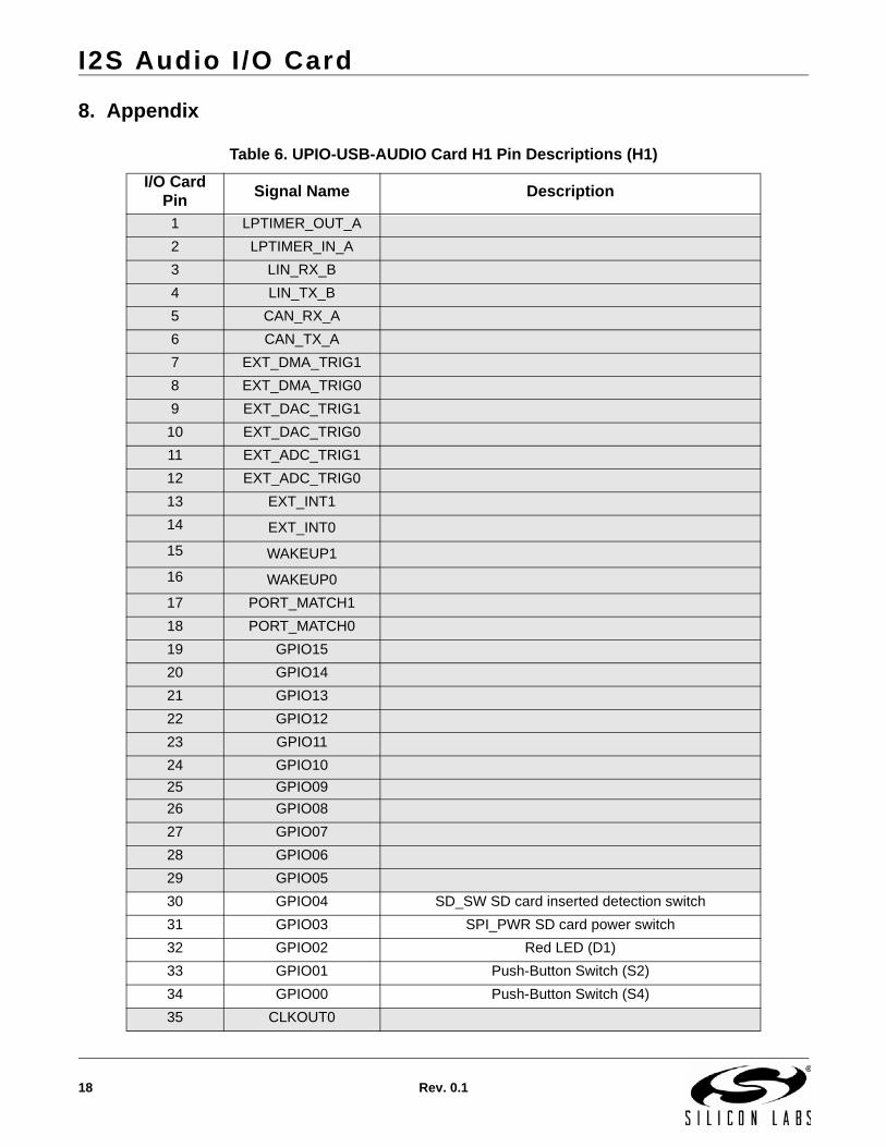
8. Appendix
Table 6. UPIO-USB-AUDIO Card H1 Pin Descriptions (H1)
I/O CardPin
Signal Name Description
1 LPTIMER_OUT_A
2 LPTIMER_IN_A
3 LIN_RX_B
4 LIN_TX_B
5 CAN_RX_A
6 CAN_TX_A
7 EXT_DMA_TRIG1
8 EXT_DMA_TRIG0
9 EXT_DAC_TRIG1
10 EXT_DAC_TRIG0
11 EXT_ADC_TRIG1
12 EXT_ADC_TRIG0
13 EXT_INT1
14 EXT_INT0
15 WAKEUP1
16 WAKEUP0
17 PORT_MATCH1
18 PORT_MATCH0
19 GPIO15
20 GPIO14
21 GPIO13
22 GPIO12
23 GPIO11
24 GPIO10
25 GPIO09
26 GPIO08
27 GPIO07
28 GPIO06
29 GPIO05
30 GPIO04 SD_SW SD card inserted detection switch
31 GPIO03 SPI_PWR SD card power switch
32 GPIO02 Red LED (D1)
33 GPIO01 Push-Button Switch (S2)
34 GPIO00 Push-Button Switch (S4)
35 CLKOUT0

I2S Audio I /O Card
Rev. 0.1 19
36 I2SIN_DOUT_A Codec I2S output (from codec) data (SD) (ADCDAT pin)
37 I2SIN_CLK_A Codec I2S clock (SCK)
38 I2SIN_DFS_A Codec I2S word sync (WS)
39 I2C_SCL_B
40 I2C_SDA_B
41 SPI_NSS3_EZR
42 SPI_NSS2_EZR
43 SPI_NSS1_EZR
44 SPI_NSS0_EZR SD Card DAT3/CS pin
45 SPI_MOSI_EZR SD Card CMD/MOSI pin
46 SPI_MISO_EZR SD Card DAT0/MISO pin
47 SPI_SCK_EZR SD Card CLK/SCLK pin
48 UART_CTS_SYS
49 UART_RTS_SYS
50 UART_RX_SYS
51 GND
52 UART_TX_SYS
53 UART_CTS_A
54 UART_RTS_A
55 UART_RX_A
56 UART_TX_A
57 TIMER_EX_B
58 TIMER_CT_B
59 TIMER_EX_A Codec external clock
60 TIMER_CT_A
61 I2C_SCL_EZR Codec command I2C clock
62 I2C_SDA_EZR Codec command I2C data
63 I2SOUT_DOUT_A I2S input (to codec) data (SD) (DACDAT pin)
64 I2SOUT_CLK_A Codec I2S clock (SCK)
65 I2SOUT_DFS_A Codec I2S word sync (WS)
66 PCA_CH1_B
67 PCA_CH0_B
68 PCA_ECI_B
69 PCA_CH1_A
70 PCA_CH0_A
71 PCA_ECI_A
72 LIN_RX_A
Table 6. UPIO-USB-AUDIO Card H1 Pin Descriptions (H1)
I/O CardPin
Signal Name Description

I2S Audio I /O Card
20 Rev. 0.1
73 LIN_TX_A
74 EPCA_CH5_A
75 EPCA_CH4_A
76 EPCA_CH3_A
77 EPCA_CH2_A
78 EPCA_CH1_A
79 EPCA_CH0_A
80 EPCA_ECI_A
81 USART_UCLK_B
82 USART_CTS_B
83 USART_RTS_B
84 USART_RX_B
85 USART_TX_B
86 SPI_NSS3_A
87 SPI_NSS2_A
88 SPI_NSS1_A
89 SPI_NSS0_A
90 SPI_MOSI_A
91 SPI_MISO_A
92 SPI_SCK_A
93 CAN_RX_B
94 CAN_TX_B
95 USART_UCLK_A
96 USART_CTS_A
P USART_RTS_A
98 USART_RX_A
99 USART_TX_A
100 GND
Table 6. UPIO-USB-AUDIO Card H1 Pin Descriptions (H1)
I/O CardPin
Signal Name Description

I2S Audio I /O Card
Rev. 0.1 21
Table 7. UPIO-USB-AUDIO Card H2 Pin Descriptions (H2)
I/O CardPin
Signal Name Description
1 CMOSCLK_XTAL2_A
2 CMOSCLK_XTAL1_A
3 LCD_COM7_A
4 LCD_COM6_A
5 LCD_COM5_A
6 LCD_COM4_A
7 LCD_COM3_A
8 LCD_COM2_A
9 LCD_COM1_A
10 LCD_COM0_A
11 LCD_SEG39_A
12 LCD_SEG38_A
13 LCD_SEG37_A
14 LCD_SEG36_A
15 LCD_SEG35_A
16 LCD_SEG34_A
17 LCD_SEG33_A
18 LCD_SEG32_A
19 LCD_SEG31_A
20 LCD_SEG30_A
21 LCD_SEG29_A
22 LCD_SEG28_A
23 LCD_SEG27_A
24 LCD_SEG26_A
25 LCD_SEG25_A
26 LCD_SEG24_A
27 LCD_SEG23_A
28 LCD_SEG22_A
29 LCD_SEG21_A
30 LCD_SEG20_A
31 LCD_SEG19_A
32 LCD_SEG18_A
33 LCD_SEG17_A
34 LCD_SEG16_A
35 LCD_SEG15_A
36 LCD_SEG14_A
37 LCD_SEG13_A

I2S Audio I /O Card
22 Rev. 0.1
38 LCD_SEG12_A
39 LCD_SEG11_A
40 LCD_SEG10_A
41 LCD_SEG09_A
42 LCD_SEG08_A
43 LCD_SEG07_A
44 LCD_SEG06_A
45 LCD_SEG05_A
46 LCD_SEG04_A
47 LCD_SEG03_A
48 LCD_SEG02_A
49 LCD_SEG01_A
50 LCD_SEG00_A
51 GND
52 EMIF_BE0B
53 EMIF_CS1B
54 EMIF_BE1B
55 EMIF_CS0B
56 EMIF_ALE
57 EMIF_OEB
58 EMIF_WRB
59 EMIF_A0
60 EMIF_A1
61 EMIF_A2
62 EMIF_A3
63 EMIF_A4
64 EMIF_A5
65 EMIF_A6
66 EMIF_A7
67 EMIF_A8
68 EMIF_A9
69 EMIF_A10
70 EMIF_A11
71 EMIF_A12
72 EMIF_A13
73 EMIF_A14
74 EMIF_A15
Table 7. UPIO-USB-AUDIO Card H2 Pin Descriptions (H2)
I/O CardPin
Signal Name Description

I2S Audio I /O Card
Rev. 0.1 23
75 EMIF_A16
76 EMIF_A17
77 EMIF_A18
78 EMIF_A19
79 EMIF_A20
80 EMIF_A21
81 EMIF_A22
82 EMIF_A23
83 HVGPIO7
84 HVGPIO6
85 HVGPIO5
86 HVGPIO4
87 HVGPIO3
88 HVGPIO2
89 HVGPIO1
90 HVGPIO0
91 EPCA_CH5_MOTOR
92 EPCA_CH4_MOTOR
93 EPCA_CH3_MOTOR
94 EPCA_CH2_MOTOR
95 EPCA_CH1_MOTOR
96 EPCA_CH0_MOTOR
97 EPCA_ECI_MOTOR
98 UDPBUS_SCL_A EBID SCL (C8051F990)
99 UDPBUS_SDA_A EBID SDA (C8051F990)
100 GND
Table 7. UPIO-USB-AUDIO Card H2 Pin Descriptions (H2)
I/O CardPin
Signal Name Description

I2S Audio I /O Card
24 Rev. 0.1
Table 8. UPIO-USB-AUDIO Card H3 Pin Descriptions (H3)
I/O CardPin
Signal Name Description
1 H3_100
2 H3_99
3 H3_98
4 H3_97
5 H3_96
6 H3_95
7 H3_94
8 H3_93
9 H3_92
10 H3_91
11 H3_90
12 H3_89
13 H3_88
14 H3_87
15 H3_86
16 H3_85
17 H3_84
18 H3_83
19 H3_82
20 H3_81
21 H3_80
22 H3_79
23 H3_78
24 H3_77
25 H3_76
26 H3_75
27 H3_74
28 H3_73
29 H3_72
30 H3_71
31 H3_70
32 H3_69
33 H3_68
34 H3_67
35 H3_66
36 H3_65

I2S Audio I /O Card
Rev. 0.1 25
37 H3_64
38 H3_63
39 H3_62
40 H3_61
41 H3_60
42 H3_59
43 H3_58
44 H3_57
45 H3_56
46 H3_55
47 H3_54
48 H3_53
49 JTAG_TDI_A
50 JTAG_TDO_A
51 GND
52 nc
53 C2_DAT_E C8051F380 co-processor C2D debugging data
54 C2_CLK_E C8051F380 co-processor C2CK debugging clock
55 C2_DAT_D C8051F990 EBID C2D debugging data
56 C2_CLK_D C8051F990 EBID C2CK debugging clock
57 C2_DAT_C
58 C2_CLK_C
59 C2_DAT_B
60 C2_CLK_B
61 C2_DAT_A
62 C2_CLK_A
63 EBID_NSS
64 EBID_MISO
65 EBID_MOSI
66 EBID_SCK
67 GND
68 PWR_SYS_BULK 3.3 V power supply for the EBID andco-processor devices69 PWR_SYS_BULK
70 PWR_3.3V_BULK PWR_3.3_BULK3.3 V supply used through the I/O board71 PWR_3.3V_BULK
72 PWR_3.3V_BULK
73 PWR_3.3V_BULK
Table 8. UPIO-USB-AUDIO Card H3 Pin Descriptions (H3)
I/O CardPin
Signal Name Description

I2S Audio I /O Card
26 Rev. 0.1
74 PWR_5.0_BULK 5.0 V power from the UDP motherboard
75 PWR_5.0_BULK
76 PWR_5.0_BULK
77 PWR_5.0_BULK
78 PWR_VPP_BULK
79 PWR_VPP_BULK
80 PWR_HV2_BUS
81 PWR_HV2_BUS
82 PWR_HV1_BUS
83 PWR_HV1_BUS
84 PWR_AUX_BUS
85 PWR_AUX_BUS
86 PWR_IO_BUS
87 PWR_IO_BUS
88 PWR_IO_OUT
89 PWR_IO_OUT
90 PWR_IO_IN
91 PWR_IO_IN
92 PWR_RADIO_OUT
93 PWR_RADIO_OUT
94 PWR_RADIO_IN
95 PWR_RADIO_IN
96 PWR_VDD_OUT
97 PWR_VDD_OUT
98 PWR_VDD_IN
99 PWR_VDD_IN
100 GND
Table 8. UPIO-USB-AUDIO Card H3 Pin Descriptions (H3)
I/O CardPin
Signal Name Description

I2S Audio I /O Card
Rev. 0.1 27
Table 9. UPIO-USB-AUDIO Card H4 Pin Descriptions (H4)
I/O CardPin
Signal Name Description
1 GND
2 H4_99
3 H4_98
4 H4_97
5 ITM_CLK
6 ITM_DAT3
7 ITM_DAT2
8 ITM_DAT1
9 ITM_DAT0
10 H4_91
11 EZR_GPIO4
12 EZR_GPIO3
13 EZR_GPIO2
14 EZR_GPIO1
15 EZR_GPIO0
16 EZR_VDI
17 EZR_ARSSI
18 EZR_RESET
19 EZR_SI100X_RX
20 EZR_FFIT
21 EZR_DTO
22 EZR_SI100X_TX
23 EZR_NFFS
24 EZRP_NIRQ
25 EZRP_SDN
26 GND
27 EZRP_RX_DATA_OUT
28 EZRO_RX_CLK_OUT
29 EZRP_TX_DATA_IN
30 GND
31 EZRP_CLK_IN
32 GND
33 EXTREG_BD_A
34 EXTREG_OUT_A
35 EXTREG_SN_A
36 EXTREG_SP_A

I2S Audio I /O Card
28 Rev. 0.1
37 I2V_INN_A
38 I2V_INP_A
39 GND
40 HVDA_INN_B
41 HVDA_INP_B
42 HVDA_INN_A
43 HVDA_INP_A
44 GND
45 CP_NEG_B
46 CP_POS_B
47 CP_NEG_A
48 CP_POS_A
49 CP_OUTA_A
50 CP_OUT_A
51 IDAC_B
52 IDAC_A
53 GND
54 DAC_OUT3
55 DAC_OUT2
56 DAC_OUT1
57 DAC_OUT0
58 DAC_VREFGND
59 DAC_VREF
60 GND
61 ADC_IN3
62 ADC_IN2
63 ADC_IN1 Microphone ADC input
64 ADC_IN0 Potentiometer
65 ADC_VREFGND board ground
66 ADC_VREF Microphone ADC input bias
67 GND
68 C2D_RX15_A
69 C2D_RX14_A
70 C2D_RX13_A
71 C2D_RX12_A
72 C2D_RX11_A
73 C2D_RX10_A
Table 9. UPIO-USB-AUDIO Card H4 Pin Descriptions (H4)
I/O CardPin
Signal Name Description

I2S Audio I /O Card
Rev. 0.1 29
74 C2D_RX09_A
75 C2D_RX08_A
76 C2D_RX07_A
77 C2D_RX06_A
78 C2D_RX05_A
79 C2D_RX04_A
80 C2D_RX03_A
81 C2D_RX02_A
82 C2D_RX01_A
83 C2D_RX00_A
84 C2D_TX15_A
85 C2D_TX14_A
86 C2D_TX13_A
87 C2D_TX12_A
88 C2D_TX11_A
89 C2D_TX10_A
90 C2D_TX09_A
91 C2D_TX08_A
92 C2D_TX07_A
93 C2D_TX06_A
94 C2D_TX05_A
95 C2D_TX04_A
96 C2D_TX03_A
97 C2D_TX02_A
98 C2D_TX01_A
99 C2D_TX00_A
100 GND
Table 9. UPIO-USB-AUDIO Card H4 Pin Descriptions (H4)
I/O CardPin
Signal Name Description

I2S Audio I /O Card
30 Rev. 0.1
CONTACT INFORMATIONSilicon Laboratories Inc.400 West Cesar ChavezAustin, TX 78701Please visit the Silicon Labs Technical Support web page:http://www.silabs.com/supportand register to submit a technical support request.
Silicon Laboratories and Silicon Labs are trademarks of Silicon Laboratories Inc.
Other products or brandnames mentioned herein are trademarks or registered trademarks of their respective holders.
The information in this document is believed to be accurate in all respects at the time of publication but is subject to change without notice. Silicon Laboratories assumes no responsibility for errors and omissions, and disclaims responsibility for any consequences resulting from the use of information included herein. Additionally, Silicon Laboratories assumes no responsibility for the functioning of undescribed features or parameters. Silicon Laboratories reserves the right to make changes without further notice. Silicon Laboratories makes no warranty, rep-resentation or guarantee regarding the suitability of its products for any particular purpose, nor does Silicon Laboratories assume any liability arising out of the application or use of any product or circuit, and specifically disclaims any and all liability, including without limitation conse-quential or incidental damages. Silicon Laboratories products are not designed, intended, or authorized for use in applications intended to support or sustain life, or for any other application in which the failure of the Silicon Laboratories product could create a situation where per-sonal injury or death may occur. Should Buyer purchase or use Silicon Laboratories products for any such unintended or unauthorized ap-plication, Buyer shall indemnify and hold Silicon Laboratories harmless against all claims and damages.