i n v dft-3d: what it means to “design for 3dic test”? e n ... · 32nm 22nm more than moore:...
TRANSCRIPT

I N V
E N
T I
V E
Sanjiv Taneja Vice President, R&D Silicon Realization Group
DFT-3D: What it means to “Design For 3DIC Test”?

Moore’s Law & More : Tall And Thin M
oore
’s L
aw:
Scal
ing
Bas
elin
e C
MO
S: C
PU, M
emor
y, L
ogic
130nm
90nm
65nm
45nm
32nm
22nm
More than Moore: Diversification
Analog/RF Passives HV Power Sensors Actuators Biochips
Information Processing
Digital content System-on-Chip
(SoC)
• Interacting with people and environment
• Non-digital content SoC & System-in-Package (SiP)
16nm
Source : ITRS
TSV (Through Silicon Vias) enables stacking of heterogeneous ICs in a single package
• Co-design & test across digital, analog, package
September 18, 2012 Cadence Design Systems: All Rights reserved
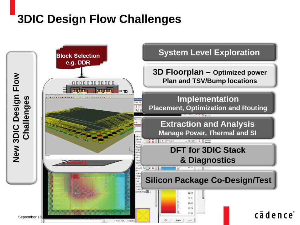
3DIC Design Flow Challenges
3D Floorplan – Optimized power Plan and TSV/Bump locations
System Level Exploration
New
3D
IC D
esig
n Fl
ow
Cha
lleng
es
Implementation Placement, Optimization and Routing
Extraction and Analysis Manage Power, Thermal and SI
DFT for 3DIC Stack & Diagnostics
Silicon Package Co-Design/Test
September 18, 2012 Cadence Design Systems: All Rights reserved

So what changes with 3DIC in EDA tools? Revamped EDA requirements
New Layout Rules (e.g. alignments)
New Layout Layer (e.g. Back Side RDL)
Thermal & mechanical
New Models, Rules
New Layout/Electrical Feature (TSV)
New Floorplanning/blockage rules
Courtesy : Qualcomm
New level of design/test integration
New level of co-design and test
3D DFT Architecture
3D Test & DFT Standardization September 18, 2012 Cadence Design Systems: All Rights reserved

New level of integration and co-design Multiple interacting requirements and features
Logic Synthesis Timing opt.
Clock gating/MSV
Analog Test Testability Analysis
ATPG/Diagnostics
Power Analysis
DFT Synthesis
September 18, 2012 Cadence Design Systems: All Rights reserved
From ‘Design-For-Test’ ‘Design-With-Test’
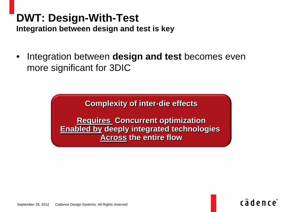
DWT: Design-With-Test Integration between design and test is key
• Integration between design and test becomes even more significant for 3DIC
Complexity of inter-die effects
Requires Concurrent optimization Enabled by deeply integrated technologies
Across the entire flow
September 18, 2012 Cadence Design Systems: All Rights reserved
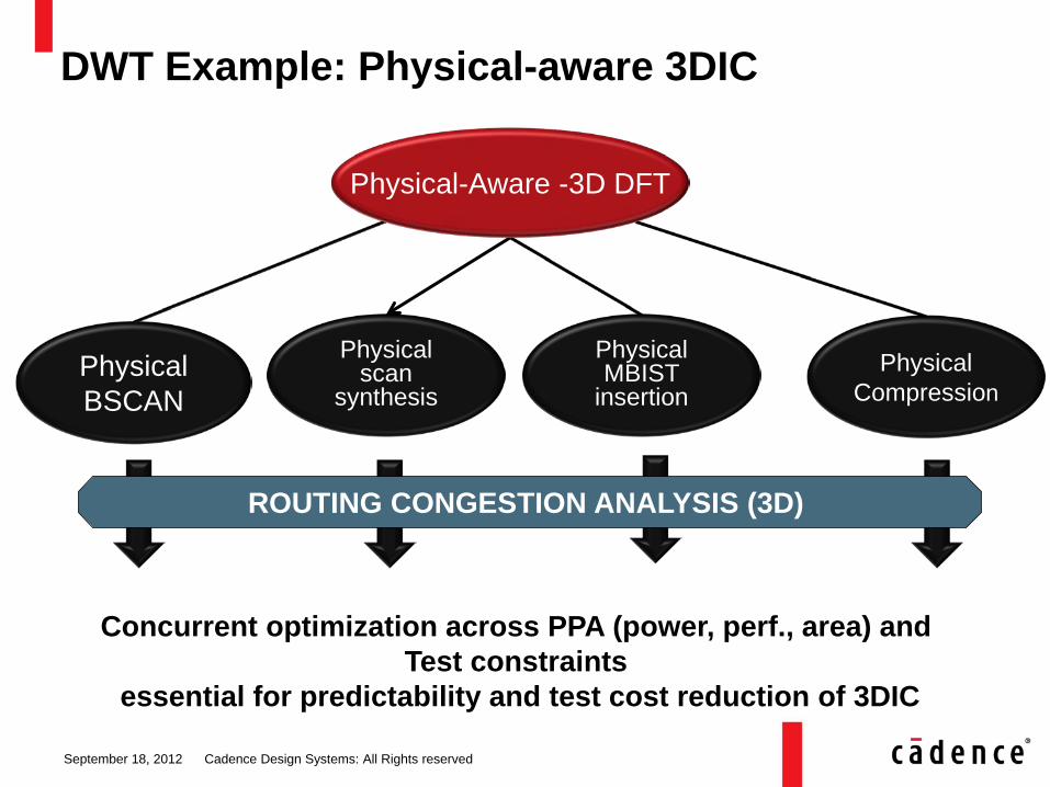
DWT Example: Physical-aware 3DIC
Physical BSCAN
Physical scan
synthesis
Physical MBIST
insertion
Physical
Compression
Physical-Aware -3D DFT
ROUTING CONGESTION ANALYSIS (3D)
Concurrent optimization across PPA (power, perf., area) and Test constraints
essential for predictability and test cost reduction of 3DIC
September 18, 2012 Cadence Design Systems: All Rights reserved

Physical-Aware Compression
8
Clumped logic causes congestion Challenges:
• Due to dense connectivity standard placement algorithms can “clump” compression logic causing local congestion Routing congestion
Solution: • Specialized DFT
aware congestion driven placement algorithms can mitigate congestion without disturbing signal path placement September 18, 2012 Cadence Design Systems: All Rights reserved

3D Test requirements drive DFT architecture
• Limited test access with challenges similar to SiP • New defect types (defects due to thinning, TSVs) • TSV Interconnect defects • Redundancy and repair of TSVs • Key Technical Requirements
– Ultra-low pin count compression – Reduced Pin Count Test – Pattern Fault model – 1149.1/1500 support – Creation of KGD after wafer test – A means to test the TSV interconnect between stacked die – A means to test inside the die of the stack
September 18, 2012 Cadence Design Systems: All Rights reserved

© 2010 Cadence Design Systems, Inc. All rights reserved.
Existing Design-for-Test • Core: internal scan, TDC, LBIST, MBIST, IEEE 1500 wrappers, TAMs • Stack product: IEEE Std 1149.1
3D DfT Architecture Test wrapper per die • Based on IEEE 1149.1 or 1500 • Two entry/exit points per die:
1. Pre-bond : extra probe pads 2. Post-bond : extra TSVs
10
DFT Architecture for 3D-IC Leverage existing (and emerging) standards: 1149.1/.6, 1500, P1687 (iJTAG)
Board
Die 1
Die 2
Die 3 Core 3
Core 2.1
Core 1.1 Core 1.2 Core 1.3
Core 2.2
BIS
T TD
C
TDC
TDC
TDC
IEEE 1500 IEEE 1500 IEEE 1500
IEEE 1500
IEEE 1500
IEEE 1500
TSV
TSV
TSV
TSV
TSV
TSV
TSV
TSV
TSV
TSV
TSV
TSV
TSV
TSV
TSV
TSV
pin pin pin pin pin pin
TSV
TSV
TSV
TSV
TSV
TSV
TSV
TSV pad
pad
pad
pad
IEEE 1149.1 Boundary Scan
[Marinissen et al. – VTS’10 / 3DIC’10]
Functional Design • ≥2 stacked dies, possibly core-based • Inter-connect: TSVs • Extra-connect: pins

© 2010 Cadence Design Systems, Inc. All rights reserved. 11
Test Generation for 3D-IC Supports Silicon Interposer Flow
3D DFT on Die-Level • Insertion of 3D wrapper • Creating Test patterns • Verification and Simulation
Testing Die Interconnects • ATPG for die interconnects
Testing Die in a stack • Modular Test approach • ATPG-on-top test approach

3-D Test and DFT Standardization
• 59 participants from companies/institutes around the globe – Chair: Erik Jan Marinissen (IMEC)
Source: Erik Jan Marinessen (IMEC)
September 18, 2012 Cadence Design Systems: All Rights reserved

Cadence Silicon-Proven 3D-IC Solution Plan Implement Test Verify
• Allows heterogeneous integration to offer power, performance in smallest form factor
• Cadence is technology leader providing
Complete & Integrated 3D-IC solution • Plan->Implement->Test->Verify • 1st to market wide I/O memory controller
• Developed in close partner-collaboration for past 3 years with Leading foundries and customers
• Multiple 3D-IC tapeouts
• Multiple test chips: Memory over logic (28 nm), logic over analog, logic over Logic, 3-stack dies
• Production design tape-out in mid-2010 Riko Radojcic, Qualcomm
September 18, 2012 Cadence Design Systems: All Rights reserved
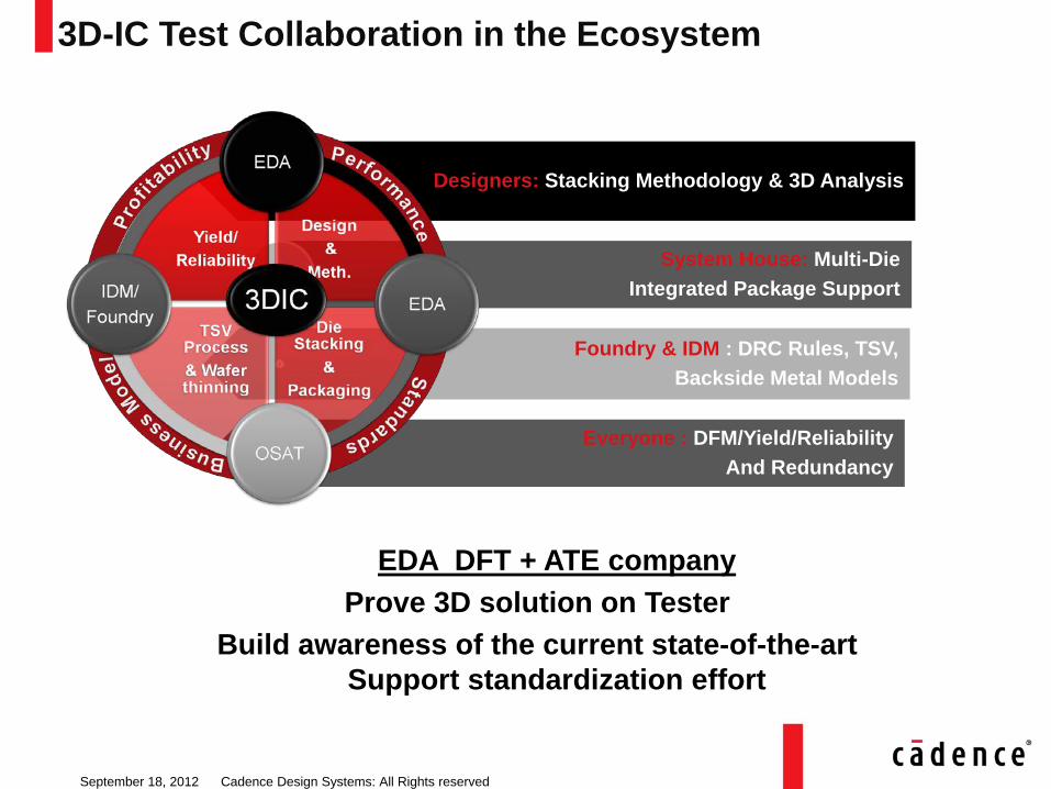
Designers: Stacking Methodology & 3D Analysis
System House: Multi-Die Integrated Package Support
Foundry & IDM : DRC Rules, TSV, Backside Metal Models
Everyone : DFM/Yield/Reliability And Redundancy
3D-IC Test Collaboration in the Ecosystem
September 18, 2012 Cadence Design Systems: All Rights reserved
EDA DFT + ATE company Prove 3D solution on Tester
Build awareness of the current state-of-the-art Support standardization effort
Questions to ponder ?
New failure mode with TSV Failures due to Thermal and Mechanical stress
Cost Management of 3D-IC system Lowest cost point : additional silicon area for DFT
versus tester time
Over heating or failed IC : Parallel testing, High-speed testing
How to avoid costly failures 15