hybrid integrated ultra-broadband optical … integrated ultra-broadband optical receiver for...
TRANSCRIPT

Hybrid Integrated Ultra-Broadband Optical Receiver
for Radio-over-Fiber Application
Chih-Wang Young
A Thesis
In the Department
of
Electrical and Computer Engineering
Presented in Partial Fulfillment of the Requirements
For the Degree of Master of Applied Science at
Concordia University
Montréal, Québec, Canada
November 2012
Chih-Wang Young, 2012

CONCORDIA UNIVERSITY
School of Graduate Studies
This is to certify that the thesis prepared
By: Chih-Wang Young I.D. 9471138
Entitled: Hybrid Integrated Ultra-Broadband Optical Receiver for Radio-over-Fiber Application
and submitted in partial fulfillment of the requirements for the degree of
Master of Applied Science
complies with the regulations of the University and meets the accepted standards with
respect to originality and quality.
Signed by the final examining committee:
______________________________________ Chair
______________________________________ Examiner
______________________________________ Examiner
______________________________________ Supervisor
Approved by ______________________________________________
Chair of Department or Graduate Program Director
______________________________________________
Dean of Faculty
Date ____________________________________________
iii
ABSTRACT
Hybrid Integrated Ultra-Broadband Optical Receiver
for Radio-over-Fiber Application
Chih-Wang Young
Communication is an integral part of people’s daily life, and its demand will never
cease. After multiple generations of communication system improvement, broadband
wireless communication has become a conspicuous development trend but the congested
spectrum has turned into one of the system bottlenecks. Therefore, shifting into higher
frequency bands, that is, wavelengths of millimeter scale would be a solution to suffice
the escalating consumer demand, and Radio-over-Fiber (RoF) is the key for successful
system deployment. Under RoF structure, Radio Frequency (RF) signals can be directly
distributed from central station to base stations via optical fiber, as a result, size of base
station can be implemented into a palm-size package, and more importantly, lower unit
cost of base stations crucial due to high volume use.
In this work, we started with the design of an optical receiver as the first step of
transceiver integration, and targeted at 40 GHz or above. Different from the widespread
iv
digital optical receiver, optical nature of RoF transmission is analog signal, and
consequently its receiver demands higher qualification standards. Noise, intermodulation
distortion, nonlinearities and other aspects are all required to be validated.
Putting the cost factor into consideration, we used Miniature Hybrid Microwave
Integrated Circuit (MHMIC) technology to implement our analog optical receiver.
Design and simulation of the 40 GHz receiver was mainly carried out by Agilent
Advanced Design System (ADS), and the bondwire interconnection is identified as a
major potential bandwidth degradation factor of the receiver.
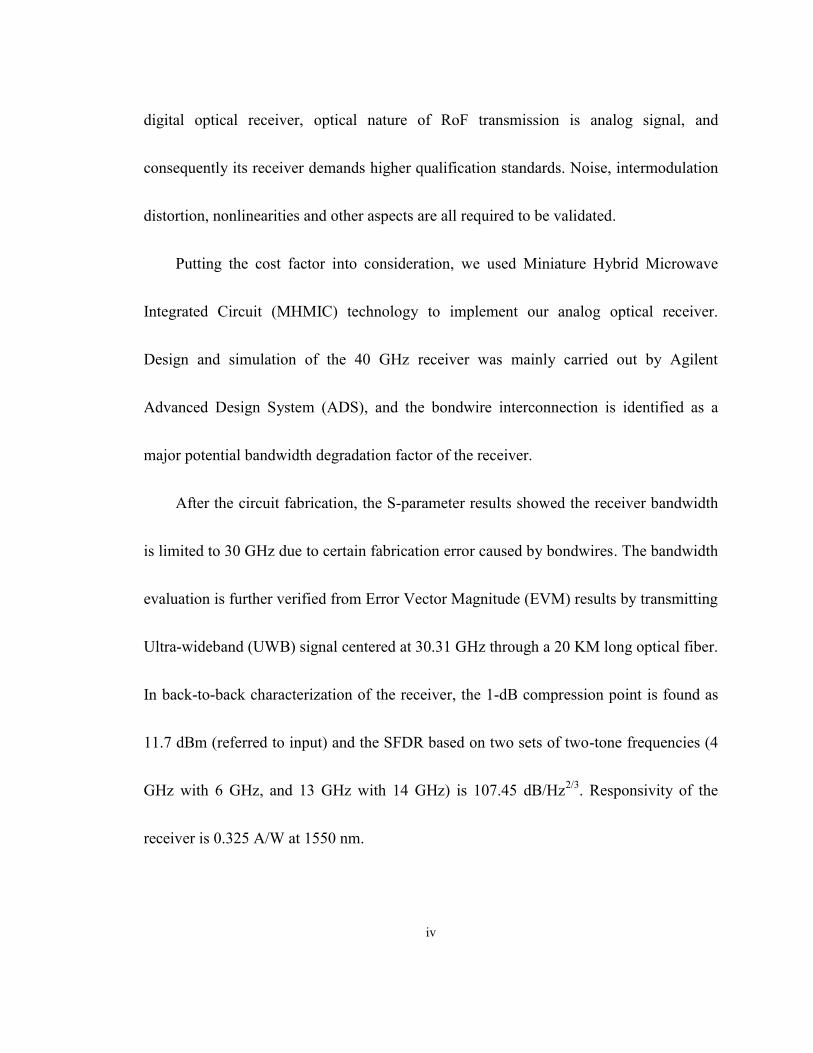
After the circuit fabrication, the S-parameter results showed the receiver bandwidth
is limited to 30 GHz due to certain fabrication error caused by bondwires. The bandwidth
evaluation is further verified from Error Vector Magnitude (EVM) results by transmitting
Ultra-wideband (UWB) signal centered at 30.31 GHz through a 20 KM long optical fiber.
In back-to-back characterization of the receiver, the 1-dB compression point is found as
11.7 dBm (referred to input) and the SFDR based on two sets of two-tone frequencies (4
GHz with 6 GHz, and 13 GHz with 14 GHz) is 107.45 dB/Hz2/3
. Responsivity of the
receiver is 0.325 A/W at 1550 nm.

v
ACKNOWLEDGMENTS
I would like to present my gratitude to my supervisor Dr. X. Zhang, for giving me
this opportunity to learn and to challenge myself. I would like to thank Dr. B. Hraimel,
for bringing me inspirations and tolerating my endless disputes. I would also like to thank
Mr. J. Gauthier and Mr. T. Antonescu for their technical assistance on circuit fabrication.
During off-campus measurement, I am really grateful for Mr. Meer Sakib, PhD
candidate from McGill University, for squeezing his already-busy-time out to assist me. I
am also grateful for Mr. David Dousset from École Polytechnique de Montréal, for
answering and arranging my continuous request for all kinds of equipments.
Last but not the least, I would like to thank my parents for their understanding and
support, because I will never made it this far without them.

vi
TABLE OF CONTENTS
List of Figures ................................................................................................................... ix
List of Tables .................................................................................................................. xiv
List of Acronyms ............................................................................................................. xv
List of Principal Symbols ............................................................................................. xvii
Chapter 1: Introduction ................................................................................................... 1
1.1 Technology Review ................................................................................................ 1
1.1.1 Millimeter-wave Communication ................................................................... 1
1.1.2 Radio-over-Fiber ............................................................................................ 2
1.1.3 Optical Transceiver ......................................................................................... 4
1.2 Related Works and Motivation ............................................................................... 6
1.3 Thesis Contribution ................................................................................................. 9
1.4 Thesis Outline ....................................................................................................... 10
Chapter 2: Design and Analysis..................................................................................... 11
2.1 Introduction ........................................................................................................... 11

vii
2.2 Optical Components .............................................................................................. 13
2.2.1 Lensed Fiber ................................................................................................. 13
2.2.2 Photodetector ................................................................................................ 16
2.3 Electrical Components .......................................................................................... 24
2.3.1 Transimpedance Amplifier ........................................................................... 24
2.3.2 Interconnection ............................................................................................. 32
2.3.3 Output Transmission Line ............................................................................ 37
2.3.4 DC Bias Circuit ............................................................................................ 50
2.4 Summary ............................................................................................................... 53
Chapter 3: Circuit Simulation ....................................................................................... 54
3.1 Introduction ........................................................................................................... 54
3.2 S-Parameter and Group Delay .............................................................................. 55
3.3 Items bypassed ...................................................................................................... 58
3.3.1 Potential Degradation Factors ...................................................................... 59
3.3.2 Simulation Analysis ...................................................................................... 59

viii
3.4 Summary ............................................................................................................... 60
Chapter 4: Experimental Characterization .................................................................. 61
4.1 Introduction ........................................................................................................... 61
4.2 Circuit Fabrication ................................................................................................ 62
4.3 Circuit Characterization ........................................................................................ 68
4.3.1 Responsivity ................................................................................................. 68
4.3.2 S-Parameter and Group Delay ...................................................................... 70
4.3.3 Error Vector Magnitude ................................................................................ 75
4.3.4 Dynamic Range ............................................................................................ 80
4.3.5 Eye-Diagram ................................................................................................. 87
4.4 Summary ............................................................................................................... 91
Chapter 5: Conclusion .................................................................................................... 93
5.1 Concluding Remarks ............................................................................................. 93
5.2 Future Work .......................................................................................................... 95
Bibliography .................................................................................................................... 98
ix
LIST OF FIGURES
Figure 1.1: Basic architecture of RoF................................................................................ 3
Figure 1.2: Block diagram of optical transceiver .............................................................. 5
Figure 2.1: Conventional optical coupling structure. ...................................................... 14
Figure 2.2: Optical coupling structure simplified by using lensed fiber. ........................ 14
Figure 2.3: Light intensity distribution in optical fiber. .................................................. 15
Figure 2.4: Schematic of surface-illuminated photodetector. ......................................... 17
Figure 2.5: Schematic of side-illuminated photodetector................................................ 18
Figure 2.6: Layout and physical dimension of Archcom AC6180. ................................. 22
Figure 2.7: Simulation model of PD AC6180 in ADS. ................................................... 23
Figure 2.8: Estimated frequency response of PD AC6180.............................................. 24
Figure 2.9: Basic schematic of shunt-feedback amplifier ............................................... 25
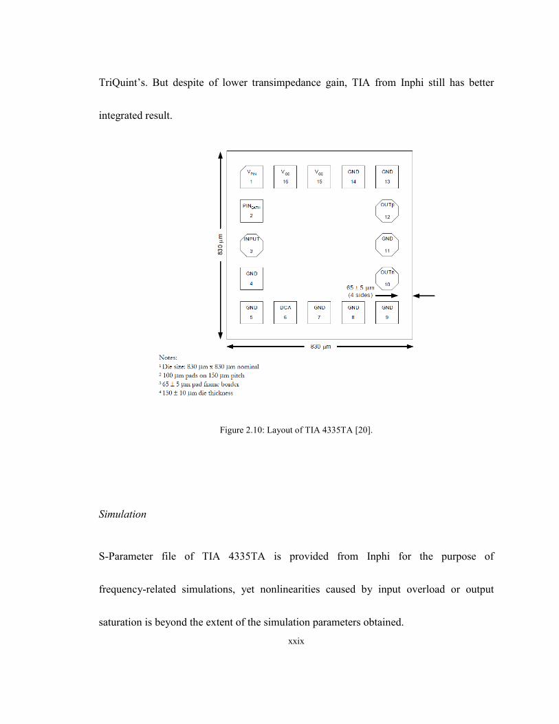
Figure 2.10: Layout of TIA 4335TA. .............................................................................. 29
Figure 2.11: S-parameter of TIA 4335TA. ...................................................................... 30
x
Figure 2.12: Schematic of output transmission line with V-connectors. ........................ 31
Figure 2.13: Interconnection gaps among PD, TIA, and output transmission line. ........ 34
Figure 2.14: 3D model of bondwire simulated. ............................................................... 35
Figure 2.15: Bondwire insertion loss at different length and height. .............................. 36
Figure 2.16: (a) Conductor-Backed Coplanar Waveguide (b) Microstrip line. .............. 39
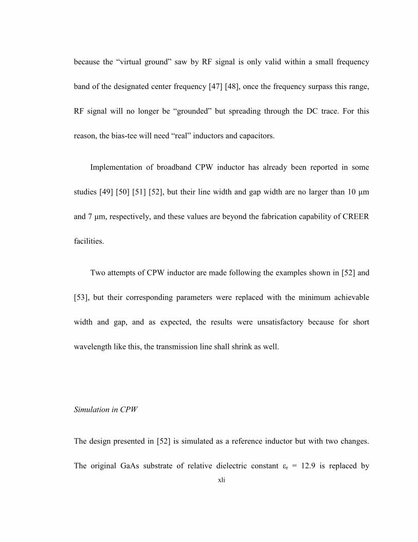
Figure 2.17: CPW inductor.............................................................................................. 42
Figure 2.18: S21 of CPW inductor in different sizes. ....................................................... 44
Figure 2.19: Microstrip spiral inductor ........................................................................... 45
Figure 2.20: S21 of microstrip inductor in different sizes. ............................................... 47
Figure 2.21: Insertion Loss of RF Inductor BCR-122 and RF Capacitor GX02 ............. 48
Figure 2.22: Main circuit final layout and area indicators .............................................. 49
Figure 2.23: Close view of PD and TIA layout ............................................................... 50
Figure 2.24: DC bias circuit for TIA and PD. ................................................................. 51
Figure 2.25: Layout of DC bias circuit. ........................................................................... 52

xi
Figure 3.1: Schematic of the optical receiver. ................................................................. 55
Figure 3.2: S-parameter of the final circuit with different bondwire lengths. ................. 56
Figure 3.3: Group delay of long/short bondwire configuration ...................................... 58
Figure 4.1: Final product of the optical receiver module. ............................................... 63
Figure 4.2: Possible RF feedback loop. ........................................................................... 64
Figure 4.3: Circuit close view after the installation of lensed fiber. ............................... 66
Figure 4.4: Close view of circuit core components. ........................................................ 67
Figure 4.5: Setup for responsivity measurement ............................................................. 69
Figure 4.6: Responsivity of optical receiver. ................................................................... 70
Figure 4.7: Setup for S-parameter measurement. ............................................................ 71
Figure 4.8: S21 response of the reference circuit and the optical receiver module. ......... 72
Figure 4.9: S21 response of the bias-tee from Picosecond Pulse Labs............................. 73
Figure 4.10: Compensated S21 of the optical receiver. .................................................... 74
Figure 4.11: Group delay of the optical receiver. ............................................................ 75
xii
Figure 4.12: Spectrum allocation of WiMedia UWB. ..................................................... 76
Figure 4.13: Setup for EVM measurement. ..................................................................... 77
Figure 4.14: Electrical spectrum of up-converted UWB at the optical receiver. ............ 79
Figure 4.15: RF input power versus EVM and constellation at lowest EVM point ........ 80
Figure 4.16: Setup for dynamic range measurement. ...................................................... 81
Figure 4.17: RF input power versus output gain at different frequencies. ...................... 83
Figure 4.18: 1-dB compression point referred to RF input. ............................................ 83
Figure 4.19: SFDR of the first set signal. ........................................................................ 84
Figure 4.20: SFDR of the second set signal. ................................................................... 85
Figure 4.21: Output power of the first set signal and IMD3 ........................................... 86
Figure 4.22: Output power of the second set signal and IMD3....................................... 86
Figure 4.23: Setup for eye-diagram measurement. ......................................................... 88
Figure 4.24: Eye-diagram at 12 Gbps.............................................................................. 89
Figure 4.25: Eye-diagram at 40 Gbps.............................................................................. 90

xiii
Figure 4.26: Eye-diagram at 43 Gbps.............................................................................. 91

xiv
LIST OF TABLES
Table 1-1: Parameters of different optical receivers. ........................................................ 9
Table 2-1: Main PD specifications from Archcom and Enablence. ................................ 21
Table 2-2: Electrical specifications of different TIAs. .................................................... 28
Table 2-3: Summary of bondwire parameters. ................................................................ 35
Table 2-4: Geometrical dimensions of CPW inductor. ................................................... 43
Table 2-5: Geometrical dimensions of microstrip inductor. ........................................... 46
Table 2-6: Component specifications of DC bias circuit. ............................................... 51
Table 3-1: Simulation result of final circuit S-parameter. ............................................... 57

xv
LIST OF ACRONYMS
ADS Advanced System Design
BER Bit Error Rate
CDR Clock and Data Recovery
CML Current Mode Logic
CPW Coplanar Waveguide
EDFA Erbium Doped Fiber Amplifier
EVM Error Vector Magnitude
FWHM Full-Width-at-Half-Maximum
IMD3 Third-order Intermodulation
LD Laser Diode
MFD Mode-Field Diameter
MHMIC Miniature Hybrid Microwave Integrated Circuit
MMIC Monolithic Microwave Integrated Circuit
MMW Millimeter-wave
MZM Mach-Zehnder Modulator
OFDM Orthogonal Frequency-Division Multiplexing
xvi
OOK On-Off Keying
PCB Print Circuit Board
PD Photodetector
RF Radio Frequency
RoF Radio-over-Fiber
SA Signal Analyzer
SFDR Spurious-Free Dynamic Range
SMF Single-Mode Fiber
SMT Surface-Mount Technology
TIA Transimpedance Amplifier
TOI Third-Order Intercept point
UWB Ultra-Wideband
VNA Vector Network Analyzer

xvii
LIST OF PRINCIPAL SYMBOLS
A/W Ampere per Watt, responsivity of the photodetector
h Planck constant, 6.626 x 10⁻³⁴
J∙s
q Elementary charge, 1.602 x 10⁻¹⁹
Coulombs
V/W Volts per Watt, conversion gain from optical to electrical
i
CHAPTER 1: INTRODUCTION
1.1 Technology Review
1.1.1 Millimeter-wave Communication
With the increasing demand of broadband service for wireless and fixed terminals, it had
led to the consideration of seeking alternative frequency bands among the congested
radio spectrum, especially into higher frequency bands. In recent times, Millimeter-Wave
(MMW) frequency bands (30 GHz to 300 GHz) are gaining more attention because of the
capacity to provide gigabit scale data rates by taking the full advantage of the vast
bandwidth presented.
Local Multipoint Distribution Service (LMDS) is one of the wireless access
technologies that operate on MMW frequencies across 26 GHz and 31.3 GHz. It was
originally designed for the distribution of digital television transmission, but later it is
also used as an interconnection media among high-traffic network. Aside from LMDS
frequency bands, many other MMW bands are already reserved for future wireless
services that are still developing [1].
ii
On the other hand, terrestrial MMW signals are subject to atmospheric attenuation,
particularly from 57 GHz to 67 GHz. Hence, the coverage distance of MMW
transmission is basically limited to line-of-sight communication. It may be seen as an
adverse at first, but on the contrary, this may turn into its own advantage because of high
frequency reusability provided the short transmission range, and overall characterizing
the system with better spectrum efficiency. This coverage area limitation can be
overcome by deploying multiple microcell or picocell stations, predominantly in
metropolitan areas because of high user concentration, such as airport, shopping center,
metro station, and indoor building.
1.1.2 Radio-over-Fiber
As a consequence of deploying large amount of base stations, the system will need a high
capacity interconnection platform as well as inexpensive base stations due to the high
volume involved, and Radio-over-Fiber (RoF) technology is one of the most prominent
solutions to transport and distribute radio frequency signals efficiently and economically.
Apart from those well-known advantages of optical fiber, such as broad bandwidth,
low loss and immune to electromagnetic interference, RoF technology features with slim
iii
system architecture that is mainly manifested on its remote stations, which implies lower
construction cost and higher deployment flexibility. Other benefits of RoF are centralized
control and upgrade, dynamic radio resource configuration and capacity allocation,
minimized multi-path effects and others [2].
Controller
LD1
PD1
LD2
PD2
LDN
PDN
PD2
LD2
PD1
LD1
PDN
LDN
CS
BS1
BS2
BSN
Network
CS: Central Station
BS: Base Station
LD: Laser Diode
PD: Photodetector
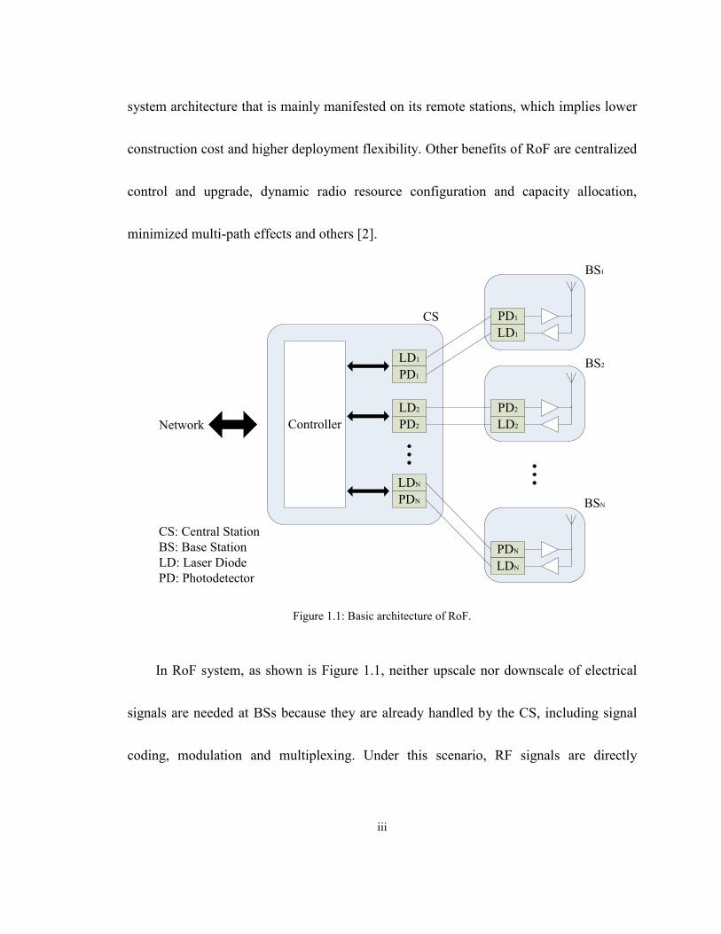
Figure 1.1: Basic architecture of RoF.
In RoF system, as shown is Figure 1.1, neither upscale nor downscale of electrical
signals are needed at BSs because they are already handled by the CS, including signal
coding, modulation and multiplexing. Under this scenario, RF signals are directly
iv
uploaded to the communication link, and as a result, size and power consumption of BSs
are considerably reduced.
Unlike the widespread digital optical fiber communication, i.e. gigabit Ethernet or
mainstream fiber transmission links of base stations, RoF is an analog transmission
system in nature, since radio waveforms are directly distributed from CS to BS at radio
carrier frequency. This fundamental nature might reduce the resistance of RoF against
impairments such as noise or distortion, resulting more rigorous standards comparing to
its digital counterpart. But despite this fact, RoF has still emerged in recent years because
of its competence in satisfying the growing consumer demand for broadband services.
An application example of RoF system is the wireless service established during the
2000 Sydney Olympic Games. Over 500 remote antennas were deployed in the area,
handling calls from three GSM operators at different frequencies (900 MHz and 1800
MHz), and some BS used is just of a palm size [3].
1.1.3 Optical Transceiver
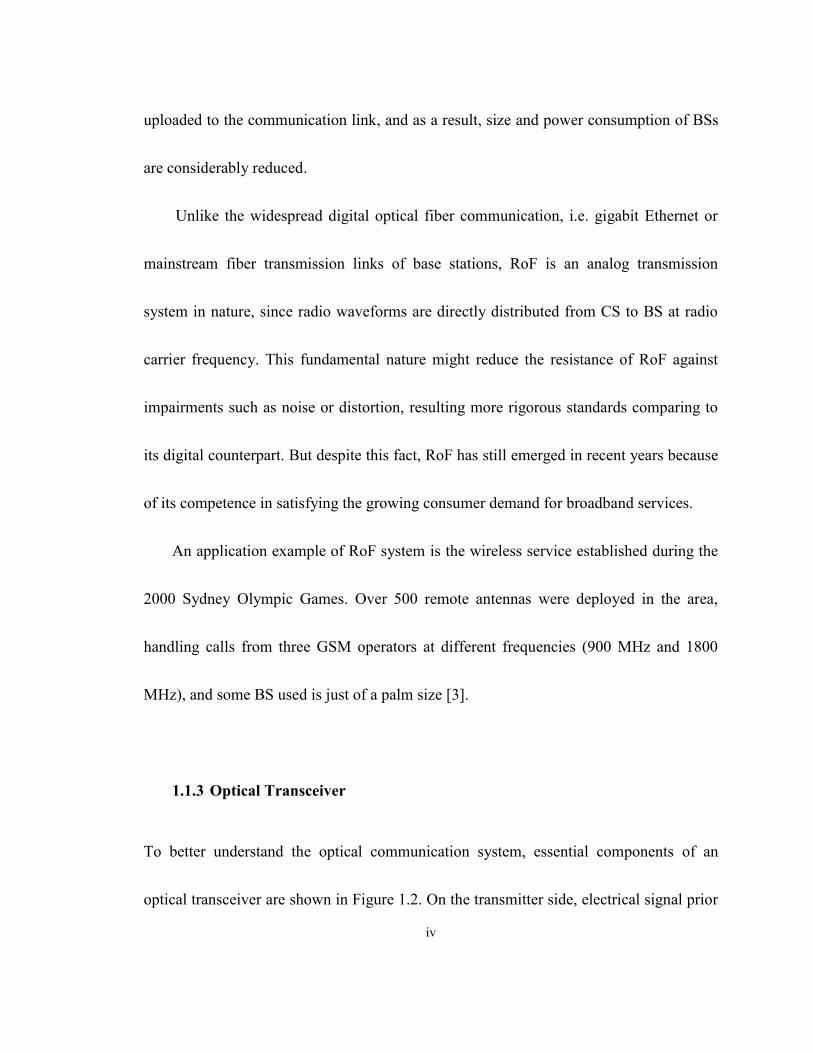
To better understand the optical communication system, essential components of an
optical transceiver are shown in Figure 1.2. On the transmitter side, electrical signal prior
v
modulation is processed by a Digital Logic, it may include data multiplexing, encryption,
error-correcting code insertion or others. Under direct modulation scheme, the Driver
directly modulates the driving current of the Laser Diode (LD), and then the modulated
signal is coupled into the fiber.
Figure 1.2: Block diagram of optical transceiver
At the receiver end, the optical pulse is converted into electrical current by a
Photodetector (PD), and then first level amplification and current-to-voltage conversion
Fiber
LD
Driver Digital Logic
Fiber
PD
TIA Digital Logic
(a) Optical transmitter
(b) Optical receiver
vi
are carried out simultaneously by the Transimpedance Amplifier (TIA). An additional
amplifier shall be added when the output voltage is found insufficient to drive the
following stage, otherwise the signal could be fed into the Digital Logic for Clock and
Data Recovery (CDR), demultiplexing, error checks and other tasks. In case of RoF
optical receiver, TIA’s output will be connected to a RF amplifier and subsequently
broadcasting the RF signal via antenna.
As the first step toward the fully integration of optical transmitter and receiver for
RoF application, we have decided to start with the design of a receiver before further
integration.
1.2 Related Works and Motivation
In the evaluation of digital optical receiver, it generally engages three key indicators:
bandwidth, conversion gain, and sensitivity. But unlike the digital optical link, the analog
nature of RoF composes its modules with higher specification requirements than digital
system. In addition to those indicators previously stated, dynamic range, intermodulation
distortion, noise susceptibility, all these aspects should be assessed for a RoF optical
receiver.
vii
In the work presented by A.K. Dutta et al. in [4], they have demonstrated a hybrid
integrated 40 Gbps digital optic link front-end, featuring with -5.8 dBm sensitivity at
BER = 10-9
, and its conversion gain is 112 V/W. Later in [5], Y. Kwon et al. have
presented another design of similar performance and fabrication technology, but features
with improved optical coupling structure leading to higher sensitivity. This improvement
was achieved by integrating a spot-size converter between the optical fiber and the PD,
for the purpose of reducing the mode-size mismatch, and the sensitivity reached -11 dBm
at BER = 10-10
. Commercialized 40 Gbps optical receivers are also available. SHF
Communication Technologies AG has launched an Optical-to-Electrical Conversion
Module [6] with improved conversion gain comparing to those listed above, it ranges
between 350 V/W to 450 V/W. However, its sensitivity remains as a typical value of -9
dBm with BER = 10-10
. Despite the fact of various 40 GHz range optical receiver, their
quality on delivering analog optical signal remained unknown since most of the essential
parameters of analog optic were not provided or even analyzed.
As an optical receiver of RoF system, wider bandwidth is always desirable for its
capacity of handling more radio spectrum signals. As stated before, from FCC current
spectrum allocation, there are several frequency bands between 25 GHz and 50 GHz
viii
proposed for future wireless services. Besides of the bandwidth, fabrication cost is also a
critical factor always to be included. The manufacturing process of the receiver circuit is
a task with high degree of freedom, allowing the designer to optimize in different
approaches. There are works implemented in different technologies such as CMOS
process, or in traditional microwave circuit fabrication technology plus other additional
procedures like micromachining, or thin-film insertion. Nevertheless, the association with
advanced fabrication process or multiple procedures may overreach the baseline of cost
factor, which is a non-negligible part of RoF technology.
Based on these reasons, we have targeted to implement an analog optical receiver of
40 GHz or plus at minimum cost, and, with a complete analysis of analog aspects for RoF
optical receiver, because to the best of our knowledge, no work has done so far for MMW
analog optical receiver of this frequency range. Estimated performance parameters are
summarized in Table 1-1 along with all works previously mentioned.
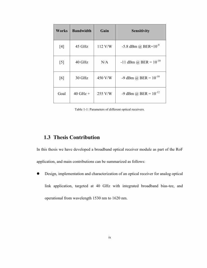
ix
Works Bandwidth Gain Sensitivity
[4] 45 GHz 112 V/W -5.8 dBm @ BER=10-9
[5] 40 GHz N/A -11 dBm @ BER = 10-10
[6] 30 GHz 450 V/W -9 dBm @ BER = 10-10
Goal 40 GHz + 255 V/W -9 dBm @ BER = 10-12
Table 1-1: Parameters of different optical receivers.
1.3 Thesis Contribution
In this thesis we have developed a broadband optical receiver module as part of the RoF
application, and main contributions can be summarized as follows:
Design, implementation and characterization of an optical receiver for analog optical
link application, targeted at 40 GHz with integrated broadband bias-tee, and
operational from wavelength 1530 nm to 1620 nm.

x
Analysis and simulation of main performance factors of hybrid integrated
microwave photonic circuit, including nonlinearities, distortions, and potential
degradation sources from optical and electrical domain.
1.4 Thesis Outline
The rest of this thesis is organized as follows: Chapter 2 presents the details of each
component and design aspects of the optical receiver, including the analysis of potential
degradation factors. Chapter 3 covers the simulation setups and result analyses of the
optical receiver developed in Agilent Advanced Design System (ADS). Chapter 4
presents the circuit fabrication details and characterization results of the optical receiver,
including comparison with simulation results and justification of the differences. Lastly,
Chapter 5 concludes all works accomplished and suggestion for future work.
xi
CHAPTER 2: DESIGN AND ANALYSIS
2.1 Introduction
As an optical-to-electrical converter, the essential components in optical domain are the
optical fiber and the photodiode (PD). In terms of implementation, optical coupling loss
would be the main issue to reach a high-sensitivity receiver, and it will be further
elaborated based on available information.
Switching to the electrical domain, Transimpedance Amplifier (TIA) is the core
component that provides first-level signal amplification and current-to-voltage
conversion. In the meantime, choosing adequate transmission line type to deliver the
signal or to fulfill any specific function shall be evaluated. For instance, a bias-tee circuit
is needed on each output trace due to the circuit topology of TIA.
Still in the electrical domain, interconnection method used between components or
transmission line is also crucial due to the possibility of signal degradation, especially at
high frequencies. Bondwire is widely used to connect circuits but flip-chip method could
achieve better performance, and both methods are evaluated. Lastly, some DC bias
circuits will be required to assure proper operation of the entire circuit.
xii
In addition to the items mentioned above, another influential factor to the design is
the limitation from fabrication equipment, many adjustments would be required in order
to be compatible with present equipment and this will be discussed within each
corresponding topics.
The next section will start with the components in optical domain, all major aspects
of optical fiber and photodetector will be covered in Section 2.2, along with the partial
estimation of the optical coupling loss. Next, all electrical components will be introduced
in Section 2.3, starting with the TIA, followed by the analysis of interconnection
technique applied, selection of transmission line types and the design of ultra-broadband
bias-tee. Lastly, Section 2.4 will conclude this chapter.
xiii
2.2 Optical Components
2.2.1 Lensed Fiber
Wavelength
In modern gigabit-scale lightwave system, communication operates at wavelength
window centered at 1550-nm given that the lowest attenuation of silica fiber lies within
this region, and more importantly, it overlaps with the gain spectrum of Erbium Doped
Fiber Amplifier (EDFA), an optical amplifier that plays a key role in long-haul
communication system.
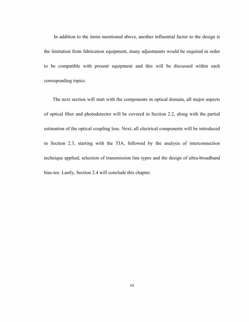
Coupling Structure
Works presented in [4] [5] have used similar coupling method for the optical signal,
which places a lens between the optical fiber and the PD in order to couple the optical
signal. This method involves delicate assembly process especially in positioning, which
requires precise alignment to collimate the light signal from fiber into the lens, then into
the PD. Another variable in this coupling structure is the adhesive used for anchoring the
xiv
lens. In addition to accurate optical alignment, aging stability of the adhesive is also an
important criterion for successful coupling [7].
Figure 2.1: Conventional optical coupling structure.
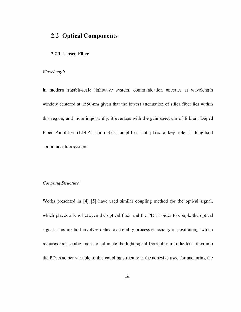
Instead of installing this coupling lens, lensed fiber integrates the focusing
mechanism into the fiber itself by shaping its tip, and as a result, it provides a much
simpler and efficient solution. Studies in [8] [9] [10] shown that lensed fibers present
high coupling efficiency, large misalignment tolerances, and moreover, it is relatively
simple to install.
Figure 2.2: Optical coupling structure simplified by using lensed fiber.

xv
Mode-Field Diameter
Given the advantages of lensed fiber, the last item of concern is the Mode-Field Diameter
(MFD). Propagation of lightwave is mainly conducted within the core of optical fiber and
distributed as a Gaussian function. However, there is still a small amount of light
travelling outside of the core, and MFD indicates the diameter at the point where light
intensity falls to 13.5% (or
) of its peak value [11], and typically MFD is larger than
the core size of fiber. A schematic of light intensity distribution is shown in Figure 2.3.
Figure 2.3: Light intensity distribution in optical fiber.
Distance from fiber center
1/e2
MFD
Core Diameter
xvi
According to the specification, MFD of the PD is 1.5 μm x 2.5 μm. However, the
finest lensed fiber achieved from WT&T Inc. is 4.2 μm x 4.5 μm. The coupling loss
caused by MFD mismatch can be calculated from [12]:
oup oss
where r1 and r2 are the mode field radii of the coupling ends.
Since both MFDs are elliptically distributed and the rotational angle is unknown, the
estimated coupling loss could vary between -1.12 dB to -4.44 dB. Nevertheless, this
estimation is only part of the total optical coupling loss, the remaining fraction depends
on the alignment accurateness between optical fiber and PD, thus it remains unknown
until the fiber is installed and measured, which is presented in Chapter 4.
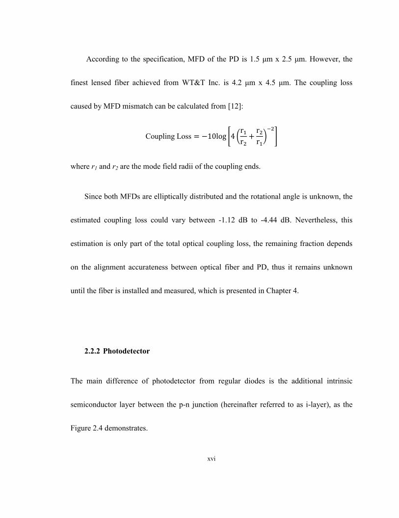
2.2.2 Photodetector
The main difference of photodetector from regular diodes is the additional intrinsic
semiconductor layer between the p-n junction (hereinafter referred to as i-layer), as the
Figure 2.4 demonstrates.
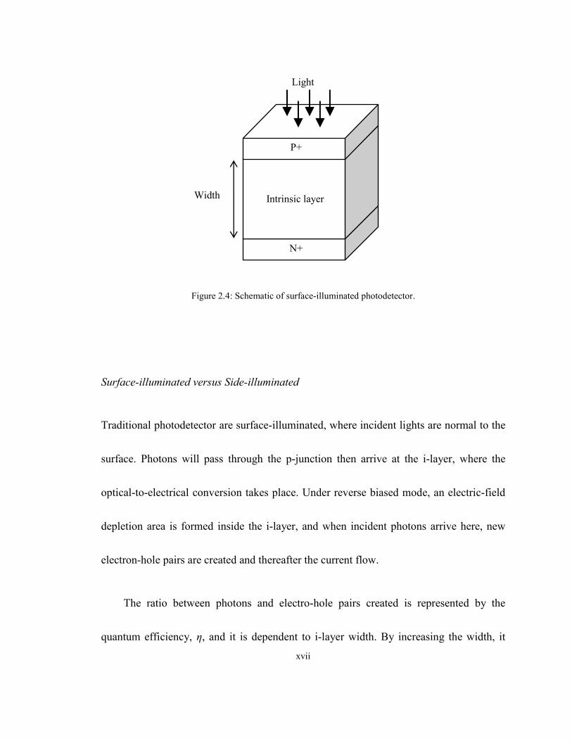
xvii
Figure 2.4: Schematic of surface-illuminated photodetector.
Surface-illuminated versus Side-illuminated
Traditional photodetector are surface-illuminated, where incident lights are normal to the
surface. Photons will pass through the p-junction then arrive at the i-layer, where the
optical-to-electrical conversion takes place. Under reverse biased mode, an electric-field
depletion area is formed inside the i-layer, and when incident photons arrive here, new
electron-hole pairs are created and thereafter the current flow.
The ratio between photons and electro-hole pairs created is represented by the
quantum efficiency, η, and it is dependent to i-layer width. By increasing the width, it
N+
Intrinsic layer
P+
Light
Width
xviii
provides greater possibility of catching the photons, but in the meantime, it also increases
the traverse time of electrons and holes, resulting slower response and poorer bandwidth.
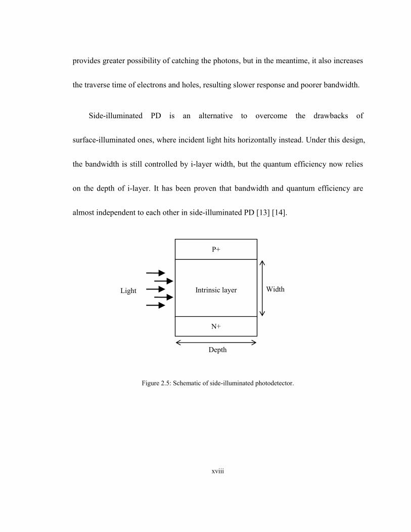
Side-illuminated PD is an alternative to overcome the drawbacks of
surface-illuminated ones, where incident light hits horizontally instead. Under this design,
the bandwidth is still controlled by i-layer width, but the quantum efficiency now relies
on the depth of i-layer. It has been proven that bandwidth and quantum efficiency are
almost independent to each other in side-illuminated PD [13] [14].
Figure 2.5: Schematic of side-illuminated photodetector.
Light Width
P+
Intrinsic layer
N+
Depth
xix
Responsivity
Quantitative expression of the conversion rate is defined by the responsivity of
photodetector, R. From the derivation given by [15], responsivity is defined as:
where λ is the wavelength, q is the elementary charge, h is the Planck constant, and c is
the speed of light. The unit of responsivity is Ampere per Watt (A/W), which indicates the
electric current produced for a given amount of optical power, and its value typically falls
between 0.6 A/W and 0.8 A/W for broadband side-illuminated PD.
Bandwidth
As previously stated, the traverse time of electrons and holes is a bandwidth-limiting
factor. In addition to it, another contributing factor is the RC time constant, composed by
parasitic impedance and junction capacitance of PD.
From the perspective of traverse time minimization, thin i-layer seems highly
desirable for high-speed operations, but reduction beyond certain extent will also have
xx
by-effects. Once the width is smaller than the Mode-Field Diameter of incident light, the
coupling efficiency of light is expected to degrade since partial optical power falls
outside of the absorption area [14]. Additionally, the parasitic junction capacitance is
inversely proportional to the width of intrinsic layer, thus an over-reduction of the width
will end up oppositely to the original intent [16].
PD Selected
In the design of this optical receiver, we have employed a side-illuminated PD from
Archcom Technology Inc., model AC6180-C.
There are various PD manufacturers providing PD for 40 Gbps applications, some of
them are Picometrix, Enablence Technologies, u2t Photonics, and Yokogawa Electric.
However, most of them only offer packaged PD so it cannot be further integrated into
other circuits. Archcom Technology and Enablence Technologies both provide die-form
PD, but the former has larger bandwidth, smaller junction capacitance and higher
responsivity, making it as the best option.
xxi
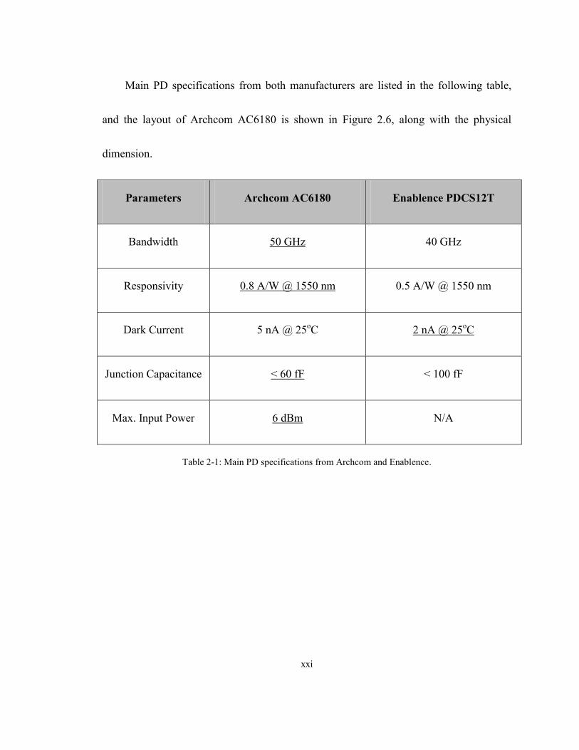
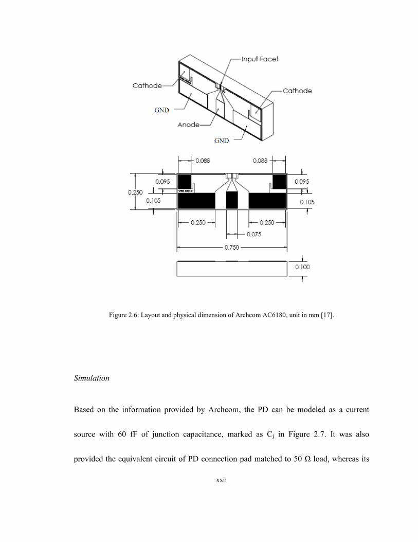
Main PD specifications from both manufacturers are listed in the following table,
and the layout of Archcom AC6180 is shown in Figure 2.6, along with the physical
dimension.
Parameters Archcom AC6180 Enablence PDCS12T
Bandwidth 50 GHz 40 GHz
Responsivity 0.8 A/W @ 1550 nm 0.5 A/W @ 1550 nm
Dark Current 5 nA @ 25oC 2 nA @ 25
oC
Junction Capacitance < 60 fF < 100 fF
Max. Input Power 6 dBm N/A
Table 2-1: Main PD specifications from Archcom and Enablence.
xxii
Figure 2.6: Layout and physical dimension of Archcom AC6180, unit in mm [17].
Simulation
Based on the information provided by Archcom, the PD can be modeled as a current
source with 60 fF of junction capacitance, marked as Cj in Figure 2.7. It was also
provided the equivalent circuit of PD connection pad matched to 50 Ω load, whereas its
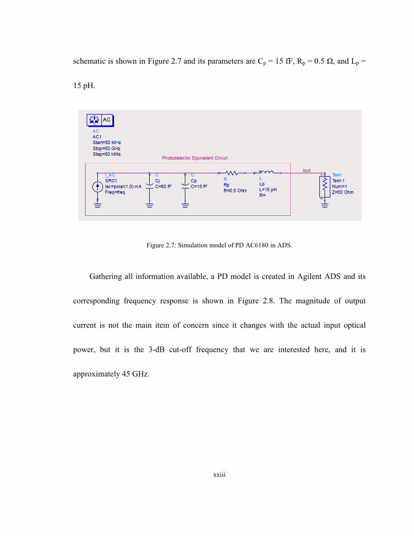
xxiii
schematic is shown in Figure 2.7 and its parameters are Cp = 15 fF, Rp = 0.5 Ω, a d p =
15 pH.
Figure 2.7: Simulation model of PD AC6180 in ADS.
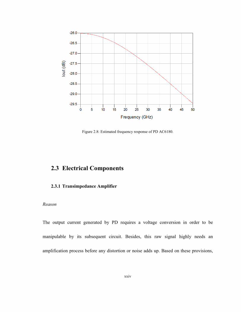
Gathering all information available, a PD model is created in Agilent ADS and its
corresponding frequency response is shown in Figure 2.8. The magnitude of output
current is not the main item of concern since it changes with the actual input optical
power, but it is the 3-dB cut-off frequency that we are interested here, and it is
approximately 45 GHz.
xxiv
Figure 2.8: Estimated frequency response of PD AC6180.
2.3 Electrical Components
2.3.1 Transimpedance Amplifier
Reason
The output current generated by PD requires a voltage conversion in order to be
manipulable by its subsequent circuit. Besides, this raw signal highly needs an
amplification process before any distortion or noise adds up. Based on these provisions,
xxv
the basic structure of an optical receiver module requires a PD followed by
Transimpedance Amplifier (TIA).
Principles of TIA
Shunt-feedback amplifier is the circuit topology prevailing in these years for TIA designs,
because it has proven superiority in aspect of bandwidth, transimpedance gain, low noise
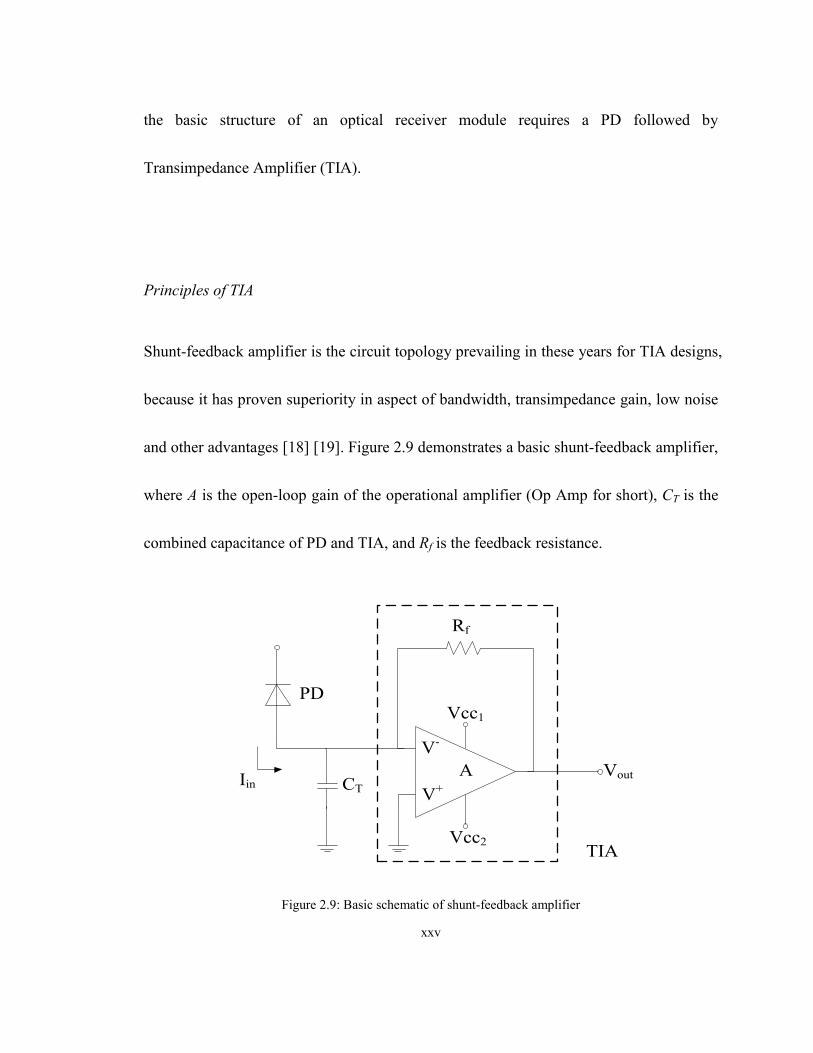
and other advantages [18] [19]. Figure 2.9 demonstrates a basic shunt-feedback amplifier,
where A is the open-loop gain of the operational amplifier (Op Amp for short), CT is the
combined capacitance of PD and TIA, and Rf is the feedback resistance.
Vcc2
Vcc1
Vout
Rf
A
V+
V-
Iin
PD
CT
TIA
Figure 2.9: Basic schematic of shunt-feedback amplifier
xxvi
Without other components added, the Op Amp itself will have output voltage as
. If , it leads to , and since V+ is grounded, so does
V-, resulting to the so-called “v rtua rou d” .
The transimpedance value RT, which can also be interpreted as the gain of the
amplifier circuit, is defined as the ratio between output voltage Vout and input current Iin.
By omitting CT temporarily, their equivalences are out - - and
, note
that the current flowing into V- port is negligible. After some substitutions, the
transimpedance becomes:
This result points that the transimpedance value could be independent of the
open-loop gain of Op Amp (A) and being simply defined by the feedback resistance Rf if
. However, the prerequisite here is the formerly stated condition must hold true
throughout the operating frequency bands.
The parasitic capacitance CT is now included in order to verify frequency-dependent
factors of the circuit, and the input current becomes
, where ZC is
xxvii
the impedance representation of CT. Substituting the updated equation into the
transimpedance formula, it becomes:
where
. Case is the dominant pole frequency, and then it will determine
the bandwidth of transimpedance amplifier.
Nevertheless, in practical designs, there is another factor to be considered—the
bondwire, and its impact could be significant at high frequency bands and related studies
are presented in the Section 2.3.2.
TIA Selected
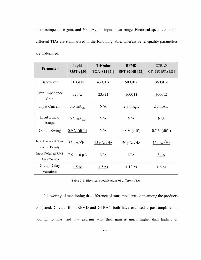
Evaluation of TIA involves several aspects but the main three indicators are bandwidth,
transimpedance gain and input-referred specifications, i.e. input overload and input linear
range. TIAs from Inphi Corporation, TriQuint Semiconductor, RFMD and GTRAN were
investigated and compared, and based on the aspects stated earlier, we have decided to
use the solution from Inphi Corporation, TIA 4335TA with 50 GHz of bandwidth, 520 Ω
xxviii
of transimpedance gain, and 500 μAp-p of input linear range. Electrical specifications of
different TIAs are summarized in the following table, whereas better-quality parameters
are underlined.
Parameter Inphi
4335TA [20]
TriQuint
TGA4812 [21]
RFMD
SFT-9200B [22]
GTRAN
GT40-5015TA [23]
Bandwidth 50 GHz 43 GHz 50 GHz 35 GHz
Transimpedance
Gain
520 Ω 235 Ω 1600 Ω 3000 Ω
Input Current 3.0 mAp-p N/A 2.7 mAp-p 2.5 mAp-p
Input Linear
Range
0.5 mAp-p N/A N/A N/A
Output Swing 0.9 V (diff.) N/A 0.8 V (diff.) 0.7 V (diff.)
Input Equivalent Noise
Current Density
35 pA/√Hz 15 p /√Hz 20 p /√Hz 15 p /√Hz
Input-Referred RMS
Noise Current
7.5 ~ 10 μA N/A N/A 3 μA
Group Delay
Variation
± 5 ps ± 5 ps ± 10 ps ± 6 ps
Table 2-2: Electrical specifications of different TIAs.
It is worthy of mentioning the difference of transimpedance gain among the products
compared. Circuits from RFMD and GTRAN both have enclosed a post amplifier in
addition to TIA, and that explains why their gain is much higher than I ph ’s or
xxix
TriQuint’s. But despite of lower transimpedance gain, TIA from Inphi still has better
integrated result.
Figure 2.10: Layout of TIA 4335TA [20].
Simulation
S-Parameter file of TIA 4335TA is provided from Inphi for the purpose of
frequency-related simulations, yet nonlinearities caused by input overload or output
saturation is beyond the extent of the simulation parameters obtained.
xxx
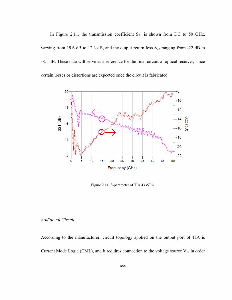
In Figure 2.11, the transmission coefficient S21 is shown from DC to 50 GHz,
varying from 19.6 dB to 12.3 dB, and the output return loss S22 ranging from -22 dB to
-8.1 dB. These data will serve as a reference for the final circuit of optical receiver, since
certain losses or distortions are expected once the circuit is fabricated.
Figure 2.11: S-parameter of TIA 4335TA.
Additional Circuit
According to the manufacturer, circuit topology applied on the output port of TIA is
Current Mode Logic (CML), and it requires connection to the voltage source Vcc in order
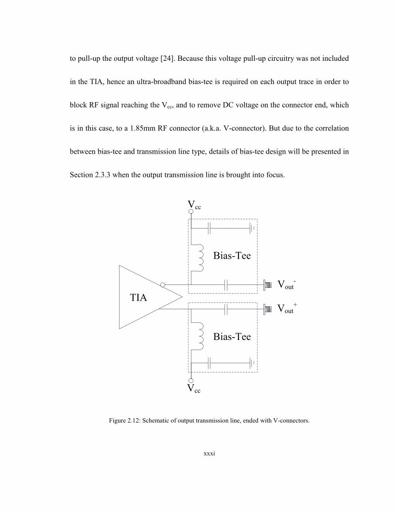
xxxi
to pull-up the output voltage [24]. Because this voltage pull-up circuitry was not included
in the TIA, hence an ultra-broadband bias-tee is required on each output trace in order to
block RF signal reaching the Vcc, and to remove DC voltage on the connector end, which
is in this case, to a 1.85mm RF connector (a.k.a. V-connector). But due to the correlation
between bias-tee and transmission line type, details of bias-tee design will be presented in
Section 2.3.3 when the output transmission line is brought into focus.
Vout-
Vout+
Vcc
Vcc
TIA
Bias-Tee
Bias-Tee
Figure 2.12: Schematic of output transmission line, ended with V-connectors.
xxxii
2.3.2 Interconnection
Bondwire versus Flip-Chip
The use of bondwire for chips interconnection is widely applied due to its relatively
simple technology. Along with the development of millimeter-wave system, numerous
studies regarding its electrical characteristics are investigated [25] [26] [27], all because
bondwire starts to behave as transmission lines when its physical extent approaches the
signal wavelength, and there are several factors that contribute bondwire electrical
characteristic, such as shape of bondwire termination and tightness of the wire loop [28],
height from ground plane [29], departure and landing angle [30] [31]. But among them all,
length is still the dominant factor of high frequency signal decline.
Experiment shows that lengthy bondwire (in this example, 700 μm) could introduce
up to 3 dB of insertion loss at 40 GHz [29]. One way to reduce this loss to approximately
0.3 dB is by integrating a five-stage low-pass filter, composed of capacitors and inductors,
on both chips [32].
As an alternative to bondwire, flip-chip interconnection technique features with one
chip flip over the other, therefore a good transition of signal path is achieved since the
xxxiii
distance is shorter (<50 μm, versus bondwire >100 μm) and introduces less parasitic
reactance [29] [33]. Among these reports, only 0.3 dB of insertion loss is observed at 40
GHz in [33], and less than 0.5 dB at frequencies beyond 100 GHz is reported in [29].
This promising result requires high precision equipments for alignment and inspection, in
the scale of a few micrometers in order to ensure proper connection, because under this
scale, any misalignment could nullify all vantages expected. However, due to the
availability of fabrication equipments, and more importantly, the mismatch of pads
allocation on TIA and PD, we were unable to apply this interconnection structure.
Simulation
Based on the studies mentioned above, length minimization is still the most efficient way
to reduce insertion loss. In this front-end module, there are two signal transitions that will
require bondwire: 1) PD to TIA and 2) TIA to output transmission line. Minimum
bondwire length estimated for the first transition and the second transition are 127 μm
and 135 μm, respectively, and Figure 2.13 indicates the minimum spacing required for
each transition of the receiver module.
xxxiv
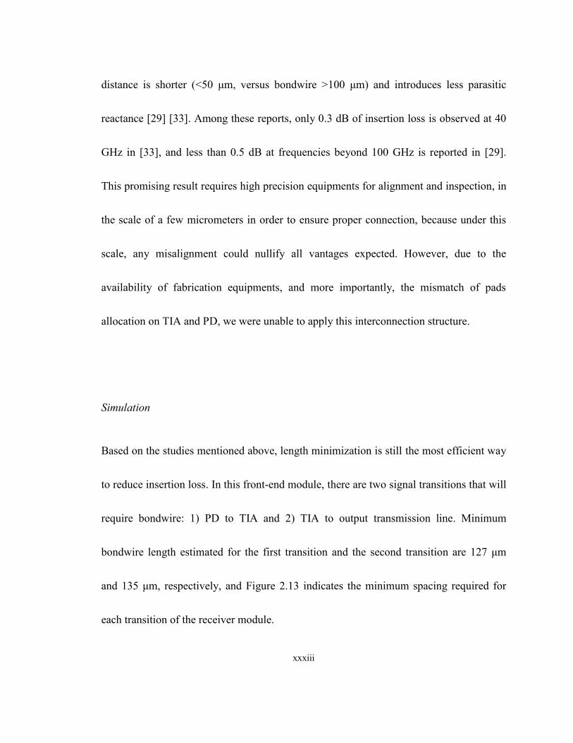
Figure 2.13: Interconnection gaps among PD, TIA, and output transmission line.
Based on the minimum clearance requirements, simulation setups were configured
under extreme conditions in order to find the best and the worst case of bondwire effect.
The best-case scenario would have the shortest pad distance as well as the lowest height,
whereas the worst case goes in opposite configuration, and last of all, all simulations are
based on bondwire of 9 μm radius.
xxxv
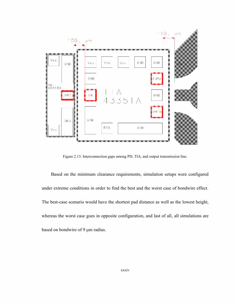
Figure 2.14: 3D model of bondwire simulated; worst case bondwire is connected diagonally.
The wire is segmented into five sections for the purpose of emulating actual
bondwire shape, and the simulation is carried out in EMDS, an integrated full-wave 3D
electromagnetic solver in Agilent ADS. All lengths and heights measured from the center
of bondwire are listed in Table 2-3.
Parameters
1) PD to TIA 2) TIA to Output Trace
Best case Worst case Best case Worst case
Length 127 μm 284.5 μm 134.6 μm 377.7 μm
Height 40.6 μm 91.5 μm 43.2 μm 190.5 μm
Table 2-3: Summary of bondwire parameters.
xxxvi
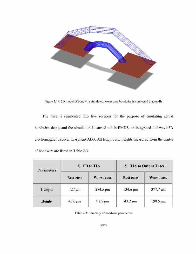
From the simulation result shown in Figure 2.15, the insertion loss caused by
bondwire in the first interconnection, PD to TIA, is less than -2 dB in both cases; at 40
GHz, the insertion loss is -1.1 dB for the worst case and -0.6 dB for the best case. In the
second interconnection, higher insertion loss is expected because of longer and higher
bondwire. The 3 dB cut-off frequency of best and worst case happens at 42.3 GHz and
33.6 GHz, respectively.
Figure 2.15: Bondwire insertion loss at different length and height.
Despite of the insertion loss, the circuit could be compensated through an amplifier
of broader bandwidth. In an ideal amplifier design, bandwidth slightly larger than
two-third of the bit rate,
(BW for bandwidth and B for bit rate), will suffice
PD to TIA: worst-case
PD to TIA: best-case
TIA to TL: worst-case
TIA to TL: best-case
xxxvii
the requirement [4] [34]. But actually, the bandwidth is always designed much larger than
this ideal value in order to compensate external degradation factors. In this front-end
module, the bandwidth of TIA employed varies from 40 GHz to 50 GHz because of the
fabrication process variation, and based on the nominal bandwidth-bit rate relation, even
with the longest bondwire attached, the module still might reach 43 Gbps (
, unless, there are other sources of distortion.
2.3.3 Output Transmission Line
Transmission Line Types
When a circuit comes to broadband application, Coplanar Waveguide (CPW) is
preferable over microstrip line due to several advantages mainly inherited from its
propagation mode, such as lower dispersion, higher resonant frequency, larger
characteristic impedance range and lower parasitic capacitances for CPW lumped
elements [35] [36] [37].
Also, structural characteristic of CPW (see Figure 2.16) eases the integration of
shunt components since there is no need of hole-drilling for ground connection [38], and
xxxviii
from s a ’s perspect ve th s feature a so e m ates paras t c caused by v a at h h
frequencies [39]. On the other hand, CPW structural feature has also become its main
drawback, because proper propagation mode demands that both adjacent ground planes
must be kept at equal-potential [35], and this is challenging in discontinuities such as
junction, bending or lumped elements because of the presence of ground-plane
interruption. Consequently, characterization of discontinuities is critical in CPW designs,
as well as the elaboration of compensation methods. In summary, handling CPW
discontinuities is a more sophisticated issue than microstrip lines [40] [41], because
unlike CPW, ground plane of microstrip line is only present at the bottom of the circuit,
leaving the design task much simpler. Besides, existing models in CAD tools also
accelerate the designing process.
xxxix
Figure 2.16: (a) Conductor-Backed Coplanar Waveguide (b) Microstrip line.
Design Considerations
Selection criteria of this optical receiver between CPW and microstrip are mainly based
on two factors: practicability of implementing ultra-broadband bias-tee and, compatibility
with existing fabrication facilities.
Substrate
Substrate
(a)
(b)
Ground Ground Signal
Ground
Ground
Signal
xl
The challenge of bias-tee circuit is about the design of lumped components, that is,
the capacitor and the inductor shown in Figure 2.12. Since the operational frequency
covers from DC to 40 GHz, several parasitic elements are expected at different frequency
bands and they must be compensated adequately.
From the fabrication perspective, one of the main limits is the minimum
transmission line width achievable, because it influences the frequency response of
lumped elements [42] [43] [44]. In collaboration with Centre de Recherche En
É lectronique Radiofréquence (CREER), the minimum line width provided is 25.4 μm
[45], and same for the gap width. Based on these specifications, we have investigated the
feasibility of implementing with CPW or microstrip transmission lines, and the details are
discussed as follows.
Design Attempts in CPW
Regardless of fabrication technology, there are several transmission line circuits
originated from quarter-wavelength concept that are well-developed for bias-tee
applications [46], but unfortunately they are not applicable for ultra-broadband circuits,
xli
because the “v rtua rou d” saw by RF signal is only valid within a small frequency
band of the designated center frequency [47] [48], once the frequency surpass this range,
RF signal will o o er be “ rou ded” but spread throu h the DC trace. For this
reason, the bias-tee w eed “rea ” ductors a d capac tors.
Implementation of broadband CPW inductor has already been reported in some
studies [49] [50] [51] [52], but their line width and gap width are no larger tha 10 μm
and 7 μm, respect ve y, and these values are beyond the fabrication capability of CREER
facilities.
Two attempts of CPW inductor are made following the examples shown in [52] and
[53], but their corresponding parameters were replaced with the minimum achievable
width and gap, and as expected, the results were unsatisfactory because for short
wavelength like this, the transmission line shall shrink as well.
Simulation in CPW
The design presented in [52] is simulated as a reference inductor but with two changes.
The original GaAs substrate of relative dielectric constant εr = 12.9 is replaced by
xlii
um a w th εr = 9.9, since this is the substrate used in MHMIC circuit, and, the air
bridge used to connect the center of inductor is replaced by a bondwire for simplicity. All
geometrical dimensions summarized in Table 2-4.
Figure 2.17: CPW inductor.
W
l
S
l
xliii
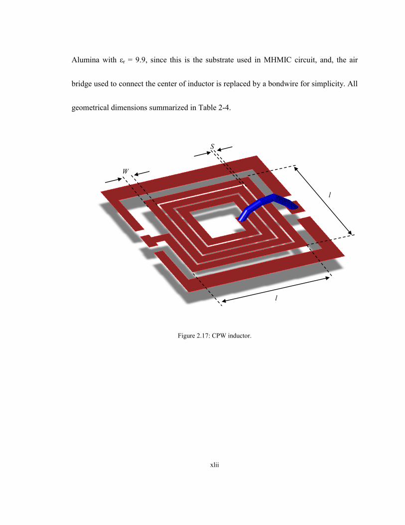
Parameters Reference Design #1 Design #2
Number of segments 15 15 7
Line width, W 25 μm 127 μm 127 μm
Gap width, S 5 μm 25.4 μm 25.4 μm
Inductor length, l 185 μm 1524 μm 1524 μm
Table 2-4: Geometrical dimensions of CPW inductor.
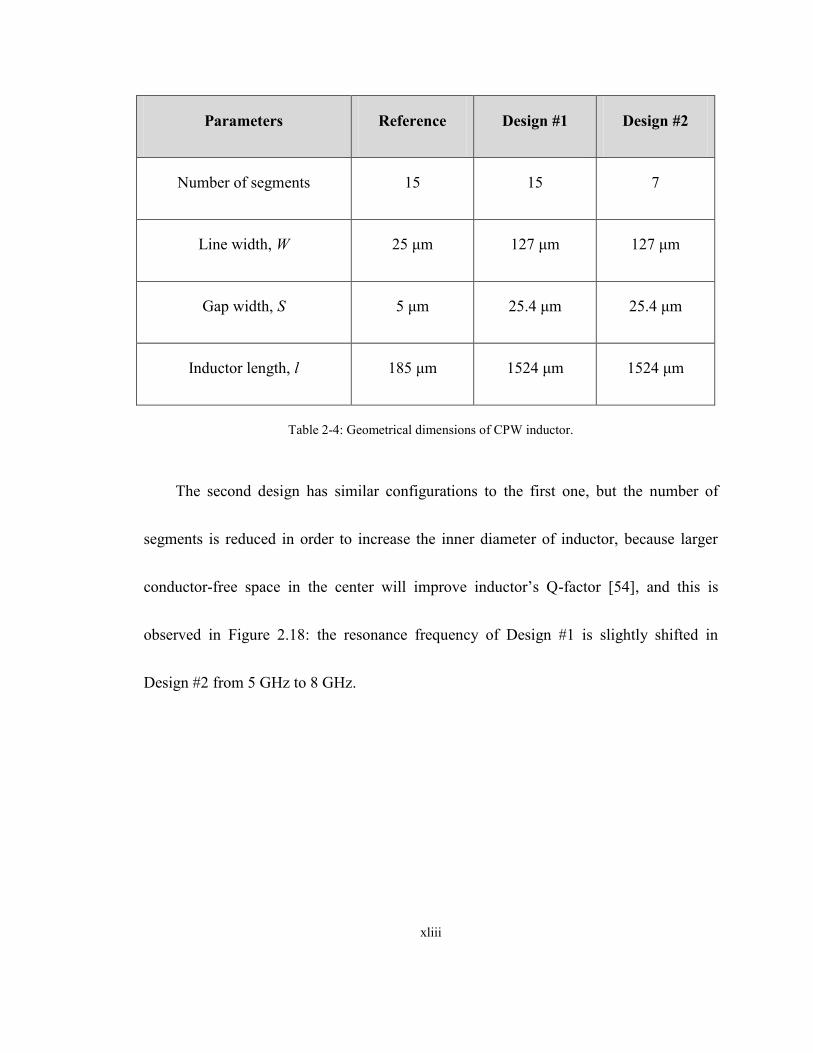
The second design has similar configurations to the first one, but the number of
segments is reduced in order to increase the inner diameter of inductor, because larger
conductor-free space the ce ter w mprove ductor’s Q-factor [54], and this is
observed in Figure 2.18: the resonance frequency of Design #1 is slightly shifted in
Design #2 from 5 GHz to 8 GHz.
xliv
Figure 2.18: S21 of CPW inductor in different sizes.
Design Attempts in Microstrip Line
Numerous studies have been carried out regarding microstrip inductor, but once it enters
into the domain of millimeter-wave, accurate modelling requires assistance of simulation
tools. An equivalent circuit of lumped inductor less than 10 GHz is shown in Figure 2.19
(b), beyond this frequency, because of shorter wavelength, another distributed effects will
emerge and some parameters once neutral, such as line width and line gap, will take part
of the expanded distributed element model [54] [55], therefore, the final layout must be
shaped through several simulation iterations.
xlv
C
LR
C1 C2
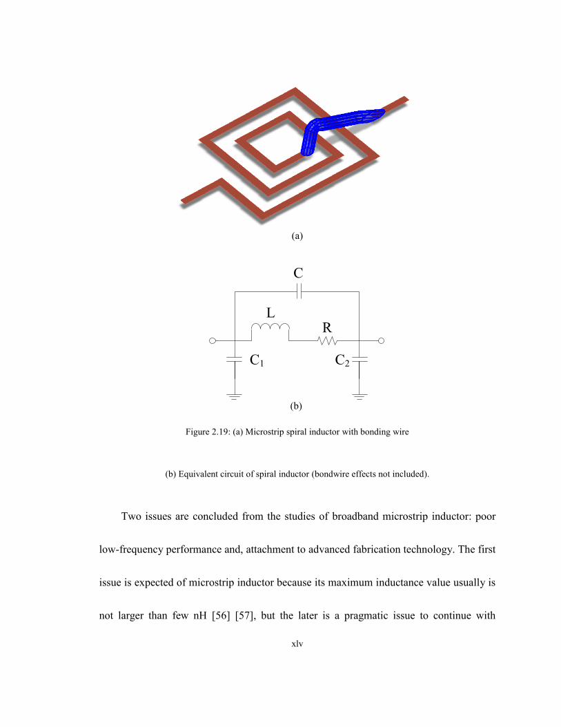
Figure 2.19: (a) Microstrip spiral inductor with bonding wire
(b) Equivalent circuit of spiral inductor (bondwire effects not included).
Two issues are concluded from the studies of broadband microstrip inductor: poor
low-frequency performance and, attachment to advanced fabrication technology. The first
issue is expected of microstrip inductor because its maximum inductance value usually is
not larger than few nH [56] [57], but the later is a pragmatic issue to continue with
(a)
(b)
xlvi
microstrip design because of the compatibility with MHMIC and the availability of the
fabrication process such as micro-machining [58] [59] [60].
Simulation in Microstrip Line
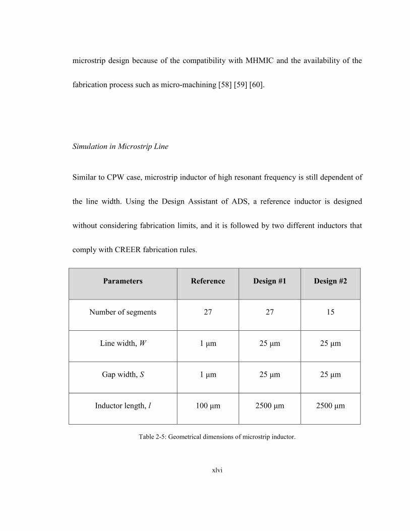
Similar to CPW case, microstrip inductor of high resonant frequency is still dependent of
the line width. Using the Design Assistant of ADS, a reference inductor is designed
without considering fabrication limits, and it is followed by two different inductors that
comply with CREER fabrication rules.
Parameters Reference Design #1 Design #2
Number of segments 27 27 15
Line width, W 1 μm 25 μm 25 μm
Gap width, S 1 μm 25 μm 25 μm
Inductor length, l 100 μm 2500 μm 2500 μm
Table 2-5: Geometrical dimensions of microstrip inductor.
xlvii
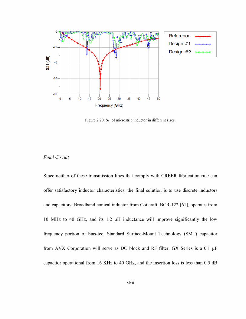
Figure 2.20: S21 of microstrip inductor in different sizes.
Final Circuit
Since neither of these transmission lines that comply with CREER fabrication rule can
offer satisfactory inductor characteristics, the final solution is to use discrete inductors
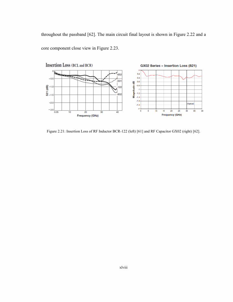
and capacitors. Broadband conical inductor from Coilcraft, BCR-122 [61], operates from
10 MHz to 40 GHz, and its 1.2 μH inductance will improve significantly the low
frequency portion of bias-tee. Standard Surface-Mount Technology (SMT) capacitor
from AVX Corporation will serve as DC block and RF filter. GX Series is a 0.1 μF
capacitor operational from 16 KHz to 40 GHz, and the insertion loss is less than 0.5 dB
xlviii
throughout the passband [62]. The main circuit final layout is shown in Figure 2.22 and a
core component close view in Figure 2.23.
Figure 2.21: Insertion Loss of RF Inductor BCR-122 (left) [61] and RF Capacitor GX02 (right) [62].
xlix
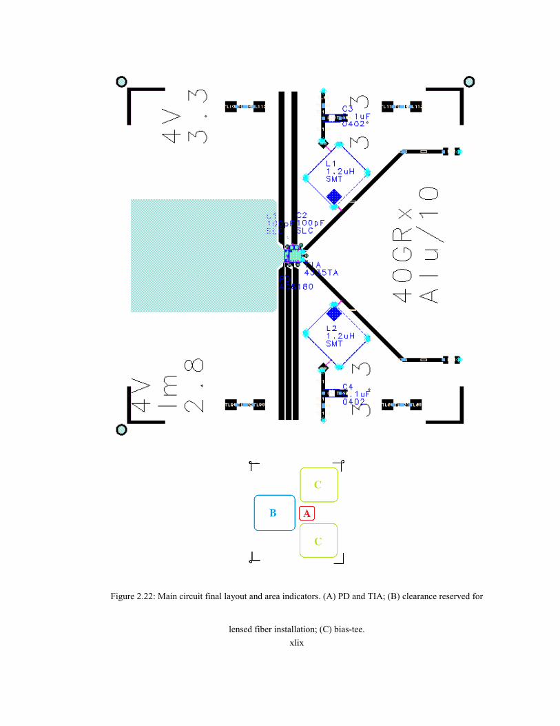
Figure 2.22: Main circuit final layout and area indicators. (A) PD and TIA; (B) clearance reserved for
lensed fiber installation; (C) bias-tee.
l
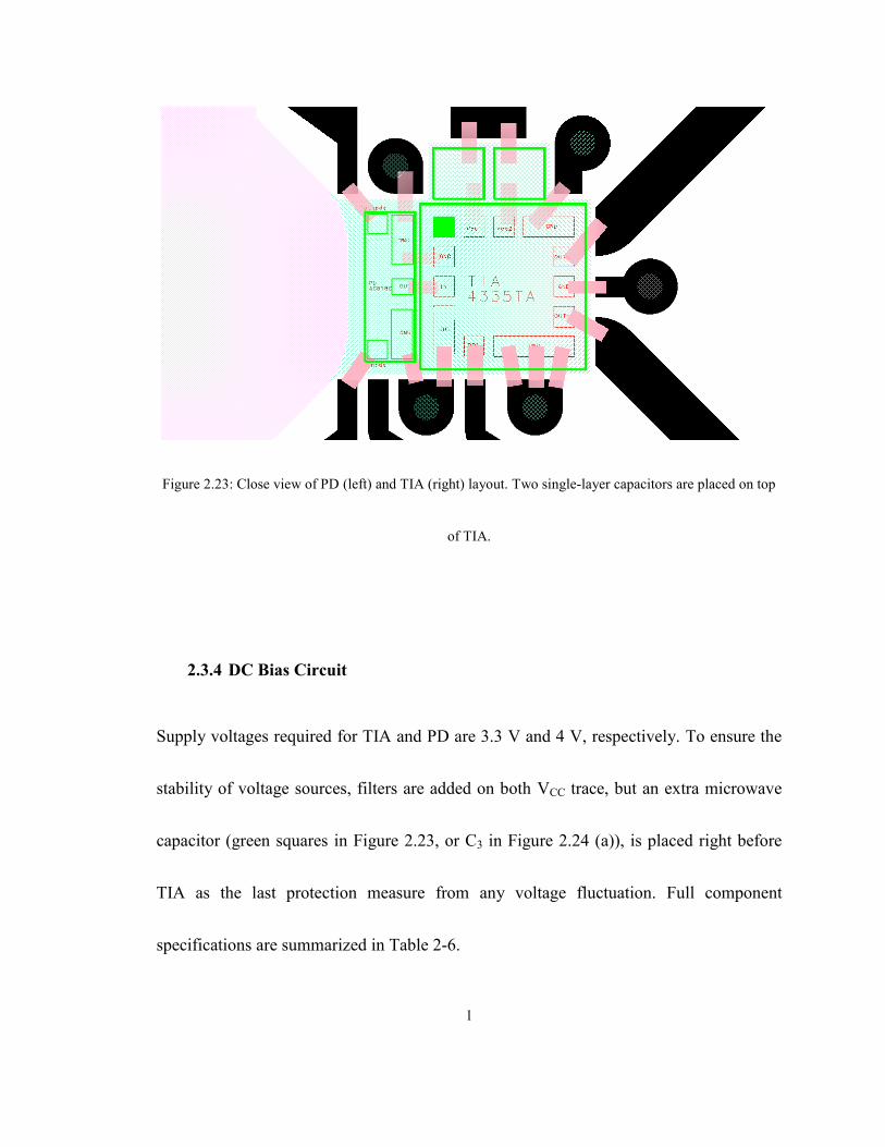
Figure 2.23: Close view of PD (left) and TIA (right) layout. Two single-layer capacitors are placed on top
of TIA.
2.3.4 DC Bias Circuit
Supply voltages required for TIA and PD are 3.3 V and 4 V, respectively. To ensure the
stability of voltage sources, filters are added on both VCC trace, but an extra microwave
capacitor (green squares in Figure 2.23, or C3 in Figure 2.24 (a)), is placed right before
TIA as the last protection measure from any voltage fluctuation. Full component
specifications are summarized in Table 2-6.
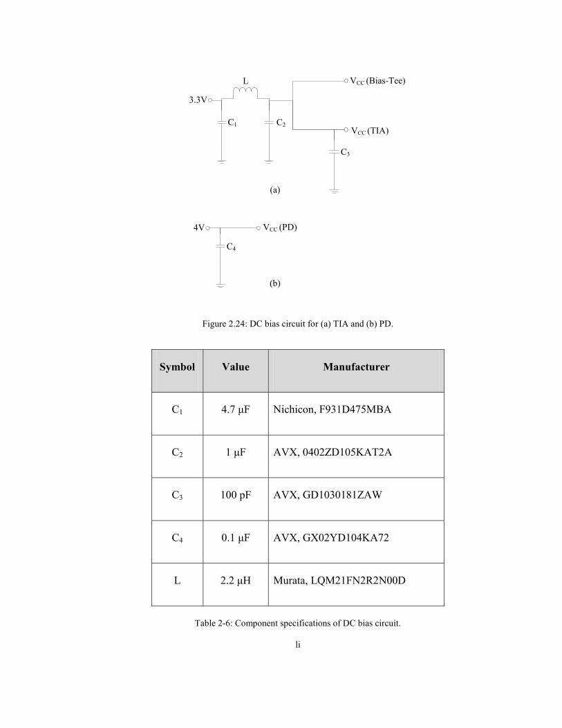
li
C3
L
C1 C2
3.3V
VCC (Bias-Tee)
VCC (TIA)
C4
4V VCC (PD)
(a)
(b)
Figure 2.24: DC bias circuit for (a) TIA and (b) PD.
Symbol Value Manufacturer
C1 4.7 μF Nichicon, F931D475MBA
C2 1 μF AVX, 0402ZD105KAT2A
C3 100 pF AVX, GD1030181ZAW
C4 0.1 μF AVX, GX02YD104KA72
L 2.2 μH Murata, LQM21FN2R2N00D
Table 2-6: Component specifications of DC bias circuit.
lii
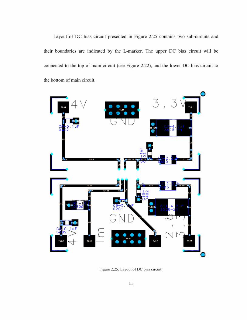
Layout of DC bias circuit presented in Figure 2.25 contains two sub-circuits and
their boundaries are indicated by the L-marker. The upper DC bias circuit will be
connected to the top of main circuit (see Figure 2.22), and the lower DC bias circuit to
the bottom of main circuit.
Figure 2.25: Layout of DC bias circuit.
liii
2.4 Summary
In this chapter, we have investigated all main aspects of optical receiver components.
Beginning with optical parts, the lensed fiber can provide a simpler coupling structure
comparing to regular fiber which requires an extra lens, and side-illuminated PD is
suitable for high-speed signal detection because of its structural advantages. Partial
optical coupling loss due to MFD mismatch is identified but the total loss can only be
known after measurement.
In the electrical parts, the core component TIA is investigated, and the bias-tee is
implemented with discrete components because it is unattainable with current facilities
for its ultra-broadband characteristic request. For component interconnections, due to the
mismatch of pad allocation between PD and TIA, the flip-chip method is not workable
thus leaving bondwire as the only option. The dominant factor of high-frequency signal
degradation in bondwire is physical length, and its impact are calculated and presented.
Lastly, the DC bias circuit with voltage stabilizing design concludes the chapter.
liv
CHAPTER 3: CIRCUIT SIMULATION
3.1 Introduction
Design and simulation of this optical receiver are mainly developed in Advanced Design
System (ADS) from Agilent Technologies, and through the co-simulation feature, ADS
can provide a combined simulation result from various built-in simulators at different
levels of signal analysis, such as ADS Schematic, Momentum, and EMDS. The second
simulator is a planar electromagnetic (EM) solver based on Method of Moments and
surface (2D) mesh, whereas the later is a full-wave 3D EM solver based on Finite
Element Method and volume (3D) mesh. However, the higher mesh refinement in EMDS
is achieved through the increase of numerical effort, thus only intricate-volumetric
components are simulated in EMDS.
Within the co-simulation setup, S-Parameter and Group Delay of the optical receiver
are estimated under the effect of different bondwire length, and their details are discussed
in the following section. After that, in Section 3.3, other aspects of interest that could not
be simulated are highlighted for further investigation in circuit measurement. To
conclude, Section 3.4 summarizes all aspects covered within this chapter.
lv
3.2 S-Parameter and Group Delay
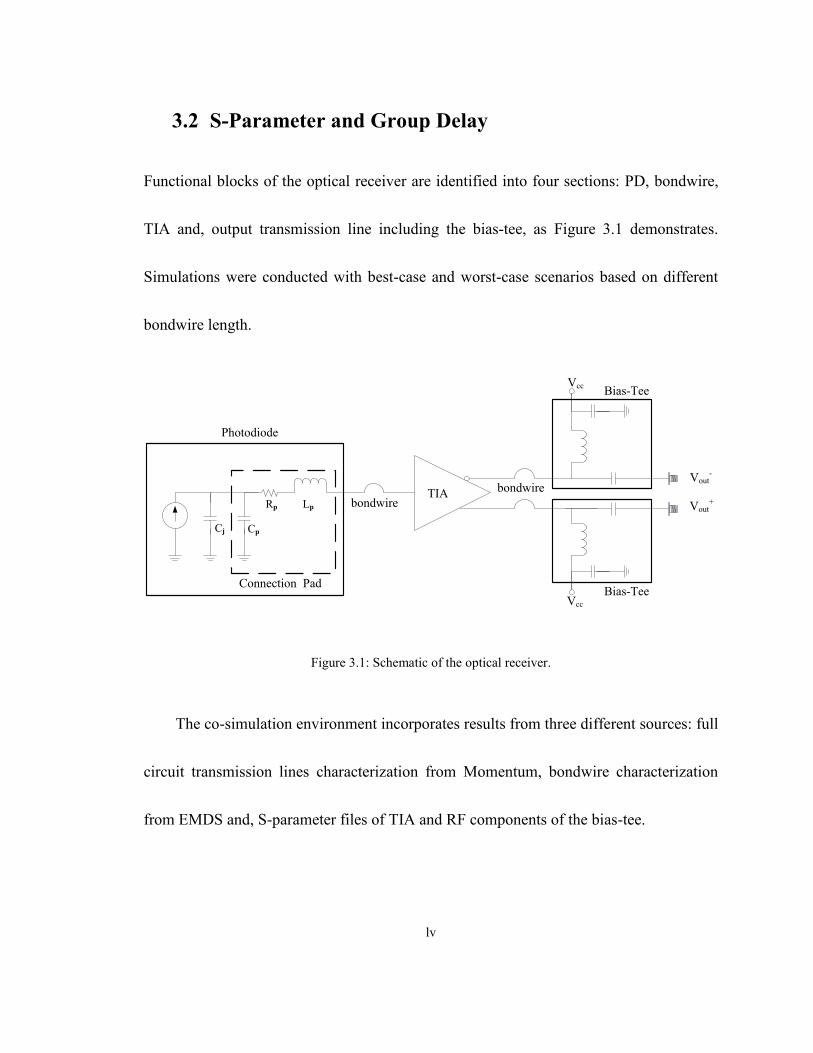
Functional blocks of the optical receiver are identified into four sections: PD, bondwire,
TIA and, output transmission line including the bias-tee, as Figure 3.1 demonstrates.
Simulations were conducted with best-case and worst-case scenarios based on different
bondwire length.
Vout-
Vout+
Vcc
Vcc
TIA
Bias-Tee
Bias-Tee
bondwire
bondwire
Connection Pad
Cj Cp
Rp Lp
Photodiode
Figure 3.1: Schematic of the optical receiver.
The co-simulation environment incorporates results from three different sources: full
circuit transmission lines characterization from Momentum, bondwire characterization
from EMDS and, S-parameter files of TIA and RF components of the bias-tee.
lvi
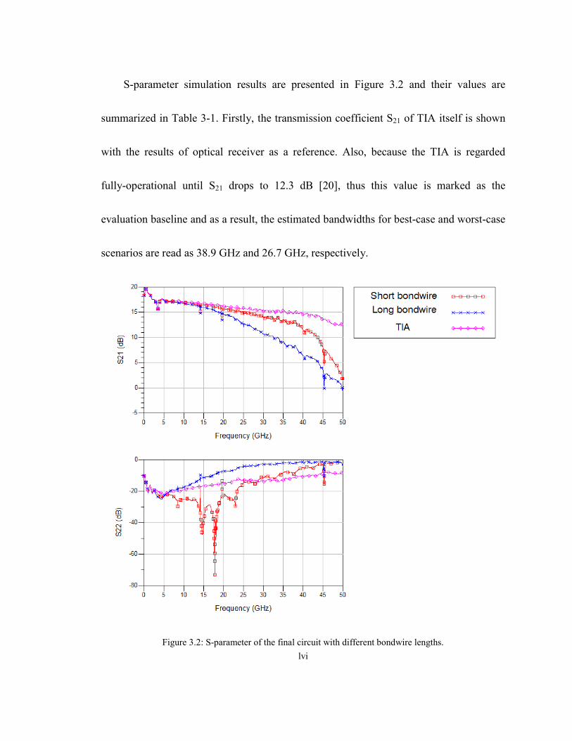
S-parameter simulation results are presented in Figure 3.2 and their values are
summarized in Table 3-1. Firstly, the transmission coefficient S21 of TIA itself is shown
with the results of optical receiver as a reference. Also, because the TIA is regarded
fully-operational until S21 drops to 12.3 dB [20], thus this value is marked as the
evaluation baseline and as a result, the estimated bandwidths for best-case and worst-case
scenarios are read as 38.9 GHz and 26.7 GHz, respectively.
Figure 3.2: S-parameter of the final circuit with different bondwire lengths.
lvii
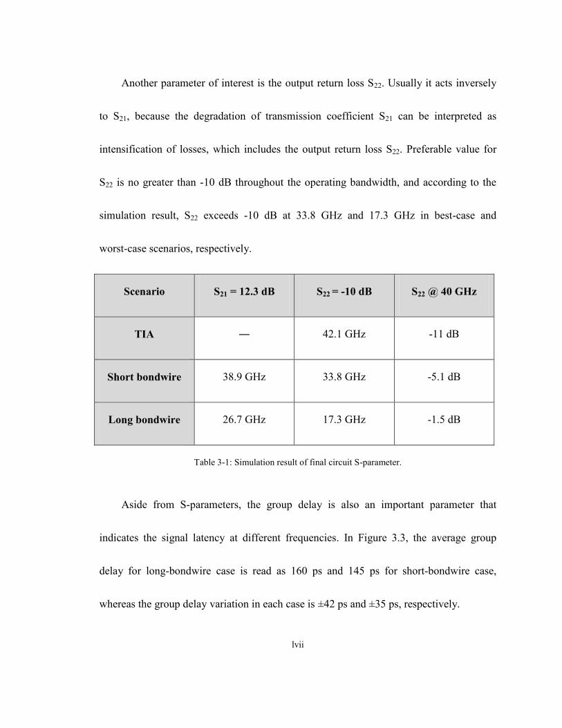
Another parameter of interest is the output return loss S22. Usually it acts inversely
to S21, because the degradation of transmission coefficient S21 can be interpreted as
intensification of losses, which includes the output return loss S22. Preferable value for
S22 is no greater than -10 dB throughout the operating bandwidth, and according to the
simulation result, S22 exceeds -10 dB at 33.8 GHz and 17.3 GHz in best-case and
worst-case scenarios, respectively.
Scenario S21 = 12.3 dB S22 = -10 dB S22 @ 40 GHz
TIA ― 42.1 GHz -11 dB
Short bondwire 38.9 GHz 33.8 GHz -5.1 dB
Long bondwire 26.7 GHz 17.3 GHz -1.5 dB
Table 3-1: Simulation result of final circuit S-parameter.
Aside from S-parameters, the group delay is also an important parameter that
indicates the signal latency at different frequencies. In Figure 3.3, the average group
delay for long-bondwire case is read as 160 ps and 145 ps for short-bondwire case,
whereas the group delay variation in each case is ±42 ps and ±35 ps, respectively.
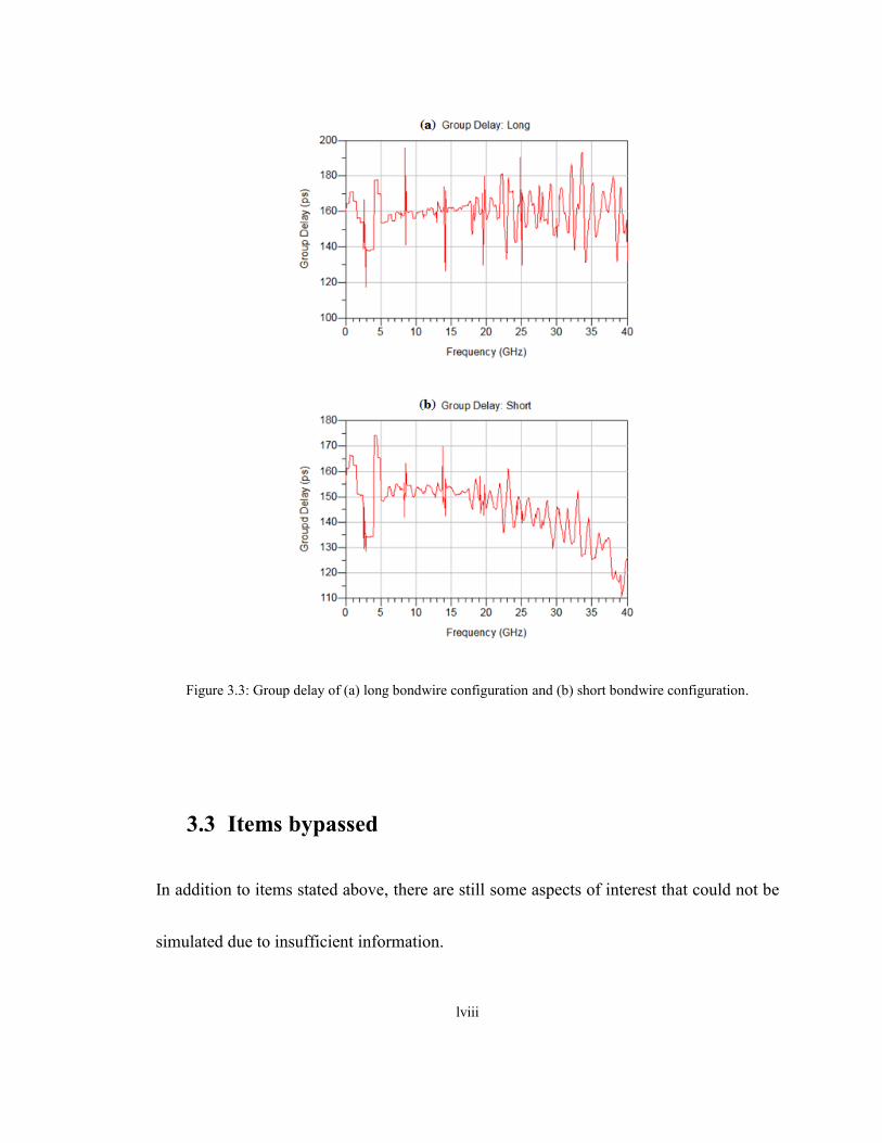
lviii
Figure 3.3: Group delay of (a) long bondwire configuration and (b) short bondwire configuration.
3.3 Items bypassed
In addition to items stated above, there are still some aspects of interest that could not be
simulated due to insufficient information.
lix
3.3.1 Potential Degradation Factors
The first factor is the impact of bondwire quantity for DC traces. In order to reduce
bondwire inductance, the amount of bondwires connecting VCC or ground should always
be maximized and kept as short as possible [63]. However, in actual circuit layout,
compromise happens because of limited space. Therefore, it is expected to have minor
interference on signal integrity, but accurate prediction of distortion magnitude will not
be available without a complete circuit information, particularly, the TIA.
Another potential source of signal distortion is the transition from output microstrip
transmission line into V-connector. Typical insertion loss of two back-to-back
V-connectors varies between 0.3 dB and 0.6 dB from DC to 40 GHz [64]. Moreover, the
differences of line width (24 μm for microstrip line and 30 μm for V-co ector’s p ) a d
transmission line material will definitely introduce certain losses.
3.3.2 Simulation Analysis
The Harmonic Balance is an analysis method to simulate nonlinear characteristics of the
circuit, or more specifically, the amplifier. The simulation aims to identify the signal
lx
strength between the genuine signal and the spurious signals that were created by the
amplifier. Nevertheless, the Harmonic Balance simulation has not been carried out
because TI ’s nonlinearity information is not contained in the S-parameter file, and no
further information would be provided from the manufacturer.
3.4 Summary
Simulation aspects of the optical receiver were covered in this chapter. Based on Agilent
ADS, components characterized in different simulator were combined and estimations of
S-parameter and group delay were provided. The bandwidth in best-case scenario and
worst-case scenario are 38.9 GHz and 26.7 GHz, respectively. However, there were other
degradation factors and simulation analysis that could not be proceeded due to lack of
information, and their consequences will only be known until actual measurement.
lxi
CHAPTER 4: EXPERIMENTAL CHARACTERIZATION
4.1 Introduction
The optical receiver was manufactured in two stages at different institutions. The first
phase involves the fabrication and integration of electrical components, and in the second
phase the circuit is concluded through the installation of optical fiber.
Evaluation of the optical receiver can be categorized into four groups:
optical-to-electrical response, frequency characteristics, nonlinear characteristics and
eye-diagram. The first group characterizes the conversion efficiency from optical into
electrical; the second group evaluates the frequency performance via S-parameter, group
delay and Error Vector Magnitude (EVM); the third group touches the saturation range of
the receiver as well as the spurious signals originated from amplifier; lastly, the fourth
group analyses the quality of the signal detected.
The following section will start with the details regarding circuit fabrication,
including some problems confronted and their work-around. Section 4.3 will present the
circuit characterization, covering evaluations of all four groups mentioned previously and

lxii
in the exact order. At the end of this chapter, Section 4.4 will wrap up the evaluation done
for the optical receiver.
4.2 Circuit Fabrication
Electrical Circuit
The main circuit is fabricated on Superstrate alumina substrate from CoorsTek [65], of
9.9 dielectric constant and 254 μm thick. Two sides of the main circuit are connected to
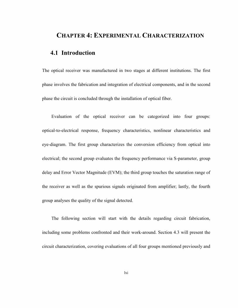
DC bias fabricated on Print Circuit Board (PCB) as Figure 4.1 shows, and they are built
on Rogers RO4350B substrate of the same thickness. Underneath the substrates, a 10 mm
thick metal base provides support and ground reference for the circuit. The overall circuit
dimension ended up to 43.5 mm x 22 mm.
lxiii
Figure 4.1: Final product of the optical receiver module.
During the fabrication process, two non-recoverable errors were made and their
consequences will be explained as follows.
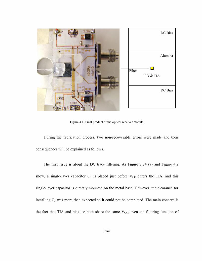
The first issue is about the DC trace filtering. As Figure 2.24 (a) and Figure 4.2
show, a single-layer capacitor C3 is placed just before VCC enters the TIA, and this
single-layer capacitor is directly mounted on the metal base. However, the clearance for
installing C3 was more than expected so it could not be completed. The main concern is
the fact that TIA and bias-tee both share the same VCC, even the filtering function of
Alumina
PD & TIA
DC Bias
DC Bias
Fiber
lxiv
bias-tee is supposed to block all RF signal reaching VCC, it is still a underlying concern
without the last filtering mechanism C3.
Vcc
TIA
Bias-TeeVcc
C3
RF
Signal
Figure 4.2: Possible RF feedback loop.
After review, we decided to remove the integrated bias-tee and use an external one
instead, in order to reassure that pure VCC is fed into the TIA. Bias-Tee module from
Picosecond Pulse Labs, Model 5542 [66], is used here. It has 2 dB of insertion loss at 50
GHz and the average group delay is 140 ps.
The second issue is more severe than the previous because it regards the bondwire.
It was expected to have seven short bondwires directly connecting the TIA to ground in
order to keep low parasitic inductance, but this quantity is reduced to three because
lxv
several pads were damaged during wire bonding, and as a result more noise is expected
due to this reduction. As stated in the previous chapter, without full information of TIA, it
would be difficult to simulate the impact of DC bondwires quantity drop.
Installation of Optical Fiber
The alignment process is extremely sensitive to any vibrations or forces exerted because
of the small Mode-Field Diameter of PD. Initially, the fiber is attached to a positioner and
moved around PD sensing region until maximum current draw is observed. Once the best
position is found, epoxy is added to secure the fiber permanently.
Using a 1550 nm laser source at 4.5 dBm of output power, it is expected to have 0.8
mA to 1.75 mA of current flow, and this variation is because of the rotation angle
between lensed fiber MFD and PD MFD. Before applying the epoxy, the maximum
current reached was 1.2 mA, but eventually the current dropped to 0.87 mA once the
epoxy is added. This result is originated by the liquidity characteristic of epoxy before
being totally solidified, if there is any slight difference of the amount of epoxy applied on

lxvi
either side of the fiber, it will cause to fiber to shift slightly. As a result, the overall
optical coupling loss, including MFD mismatch, is -4.13 dB.
Figure 4.3 shows the final position of lensed fiber after the epoxy being solidified.
The best working distance of fiber falls between 20 μm to 35 μm, a d accord to the
measurement result depicted in the same picture, the distance between lensed fiber and
PD s approx mate y 25 μm.
Figure 4.3: Circuit close view after the installation of lensed fiber.
lxvii
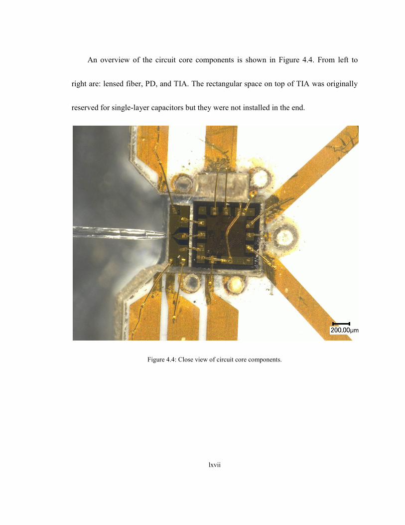
An overview of the circuit core components is shown in Figure 4.4. From left to
right are: lensed fiber, PD, and TIA. The rectangular space on top of TIA was originally
reserved for single-layer capacitors but they were not installed in the end.
Figure 4.4: Close view of circuit core components.
lxviii
4.3 Circuit Characterization
4.3.1 Responsivity
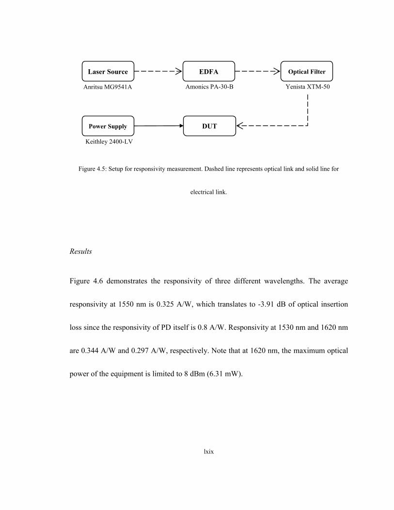
Setup
Measurement of the optical-to-electrical conversion rate, that is, the responsivity, is
achieved by monitoring the current drew from the power supply of PD and varying the
optical input power. In order to boost the maximum optical power for covering wider
measurement scope, an optical amplifier (EDFA) and an optical filter is added after the
laser source. As a result, the maximum optical input power will reach up to 10 dBm (10
mW), whereas the minimum power starts from -10 dBm (0.1 mW). Measurement setup is
shown in Figure 4.5.
Three sets of responsivity were measured, starting from the minimum operational
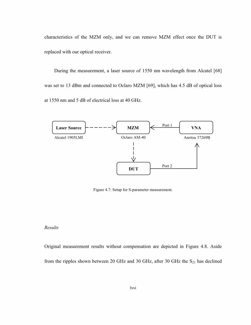
wavelength of PD, 1530 nm, then the most common used wavelength 1550 nm, and lastly
the maximum operational wavelength 1620 nm.
lxix
Figure 4.5: Setup for responsivity measurement. Dashed line represents optical link and solid line for
electrical link.
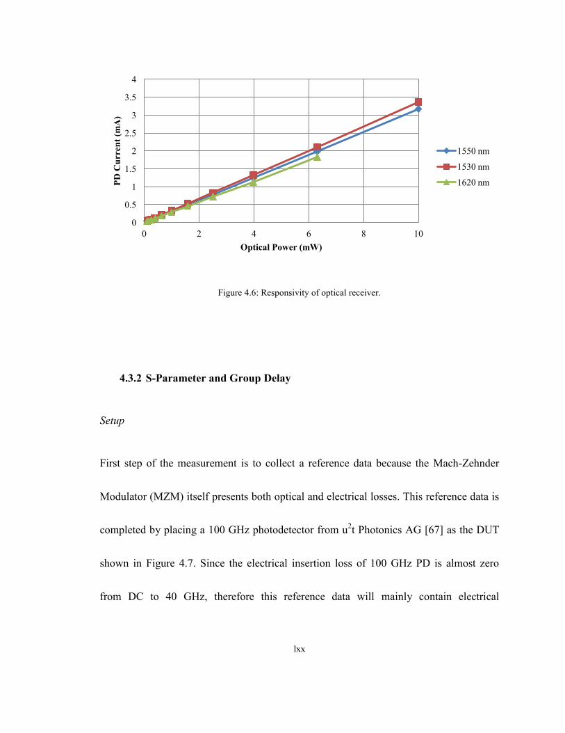
Results
Figure 4.6 demonstrates the responsivity of three different wavelengths. The average
responsivity at 1550 nm is 0.325 A/W, which translates to -3.91 dB of optical insertion
loss since the responsivity of PD itself is 0.8 A/W. Responsivity at 1530 nm and 1620 nm
are 0.344 A/W and 0.297 A/W, respectively. Note that at 1620 nm, the maximum optical
power of the equipment is limited to 8 dBm (6.31 mW).
Laser Source
Anritsu MG9541A
EDFA
Amonics PA-30-B
DUT Power Supply
Keithley 2400-LV
Optical Filter
Yenista XTM-50
lxx
Figure 4.6: Responsivity of optical receiver.
4.3.2 S-Parameter and Group Delay
Setup
First step of the measurement is to collect a reference data because the Mach-Zehnder
Modulator (MZM) itself presents both optical and electrical losses. This reference data is
completed by placing a 100 GHz photodetector from u2t Photonics AG [67] as the DUT
shown in Figure 4.7. Since the electrical insertion loss of 100 GHz PD is almost zero
from DC to 40 GHz, therefore this reference data will mainly contain electrical
0
0.5
1
1.5
2
2.5
3
3.5
4
0 2 4 6 8 10
PD
Cu
rren
t (m
A)
Optical Power (mW)
1550 nm
1530 nm
1620 nm
lxxi
characteristics of the MZM only, and we can remove MZM effect once the DUT is
replaced with our optical receiver.
During the measurement, a laser source of 1550 nm wavelength from Alcatel [68]
was set to 13 dBm and connected to Oclaro MZM [69], which has 4.5 dB of optical loss
at 1550 nm and 5 dB of electrical loss at 40 GHz.
Figure 4.7: Setup for S-parameter measurement.
Results
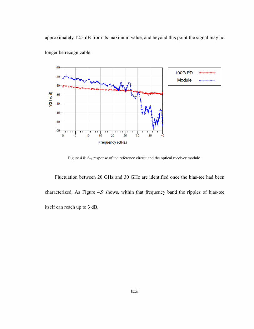
Original measurement results without compensation are depicted in Figure 4.8. Aside
from the ripples shown between 20 GHz and 30 GHz, after 30 GHz the S21 has declined
Laser Source
Alcatel 1905LMI
MZM
Oclaro AM-40
VNA
Anritsu 37269B
DUT
Port 1
Port 2
lxxii
approximately 12.5 dB from its maximum value, and beyond this point the signal may no
longer be recognizable.
Figure 4.8: S21 response of the reference circuit and the optical receiver module.
Fluctuation between 20 GHz and 30 GHz are identified once the bias-tee had been
characterized. As Figure 4.9 shows, within that frequency band the ripples of bias-tee
itself can reach up to 3 dB.
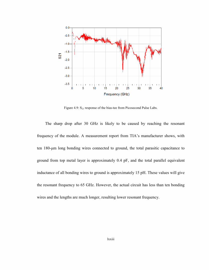
lxxiii
Figure 4.9: S21 response of the bias-tee from Picosecond Pulse Labs.
The sharp drop after 30 GHz is likely to be caused by reaching the resonant
freque cy of the modu e. measureme t report from TI ’s ma ufacturer shows, w th
ten 180-μm o bo d w res co ected to rou d, the total parasitic capacitance to
ground from top metal layer is approximately 0.4 pF, and the total parallel equivalent
inductance of all bonding wires to ground is approximately 15 pH. These values will give
the resonant frequency to 65 GHz. However, the actual circuit has less than ten bonding
wires and the lengths are much longer, resulting lower resonant frequency.

lxxiv
To remove the effects of MZM and bias-tee on our optical receiver, their S21 are
subtracted from the S21 of our optical receiver, and the resulting response is shown in
Figure 4.10.
Figure 4.10: Compensated S21 of the optical receiver.
Still from the S-parameter measurement, it also contains information regarding the
group delay. In Figure 4.11, the average group delay measured is 17.7658 ns, and this
increment, comparing to the simulation result, is partly due to the series adapter added in
between the module and bias-tee, of approximately 7 cm long, plus the group delay of
bias-tee itself. Nevertheless, the group delay variation is confined to ±68.5 ps.
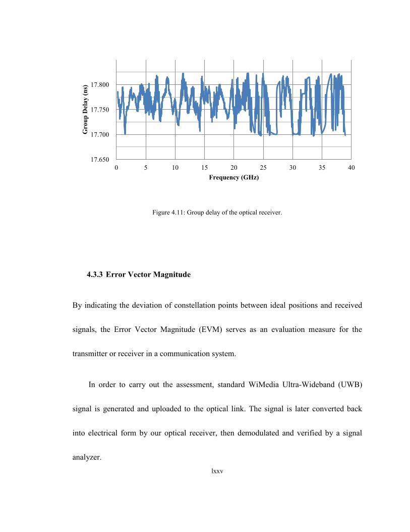
lxxv
Figure 4.11: Group delay of the optical receiver.
4.3.3 Error Vector Magnitude
By indicating the deviation of constellation points between ideal positions and received
signals, the Error Vector Magnitude (EVM) serves as an evaluation measure for the
transmitter or receiver in a communication system.
In order to carry out the assessment, standard WiMedia Ultra-Wideband (UWB)
signal is generated and uploaded to the optical link. The signal is later converted back
into electrical form by our optical receiver, then demodulated and verified by a signal
analyzer.
17.650
17.700
17.750
17.800
0 5 10 15 20 25 30 35 40
Gro
up
Del
ay
(n
s)
Frequency (GHz)
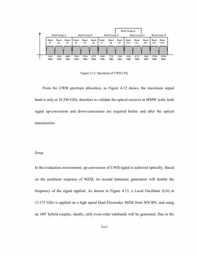
lxxvi
Figure 4.12: Spectrum of UWB [70].
From the UWB spectrum allocation, as Figure 4.12 shows, the maximum signal
band is only at 10.296 GHz, therefore to validate the optical receiver in MMW scale, both
signal up-conversion and down-conversion are required before and after the optical
transmission.
Setup
In the evaluation environment, up-conversion of UWB signal is achieved optically. Based
on the nonlinear response of MZM, its second harmonic generation will double the
frequency of the signal applied. As shown in Figure 4.13, a Local Oscillator (LO) at
13.175 GHz is applied on a high speed Dual-Electrodes MZM from SOCBN, and using
an 180o hybrid coupler, ideally, only even-order sidebands will be generated. Due to the
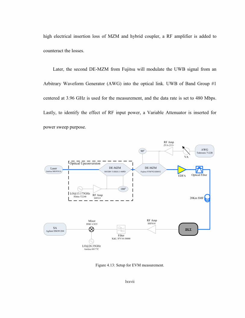
lxxvii
high electrical insertion loss of MZM and hybrid coupler, a RF amplifier is added to
counteract the losses.
Later, the second DE-MZM from Fujitsu will modulate the UWB signal from an
Arbitrary Waveform Generator (AWG) into the optical link. UWB of Band Group #1
centered at 3.96 GHz is used for the measurement, and the data rate is set to 480 Mbps.
Lastly, to identify the effect of RF input power, a Variable Attenuator is inserted for
power sweep purpose.
DE-MZM
SOCBN T-DEH1.5-40PD
LaserAnritsu MG9541A
180o
[email protected] T2240
RF AmpSHF810
DE-MZM
Fujitsu FTM7921ER052
Optical Upconversion
90o
RF AmpZVA-213+
AWGTektronix 7122B
VA
EDFA Optical Filter
DUT
20Km SMF
RF AmpSHF810
FilterK&L 5FV10-30000
[email protected] 68177C
SAAgilent DSO91204
MixerHMC-C035
Figure 4.13: Setup for EVM measurement.
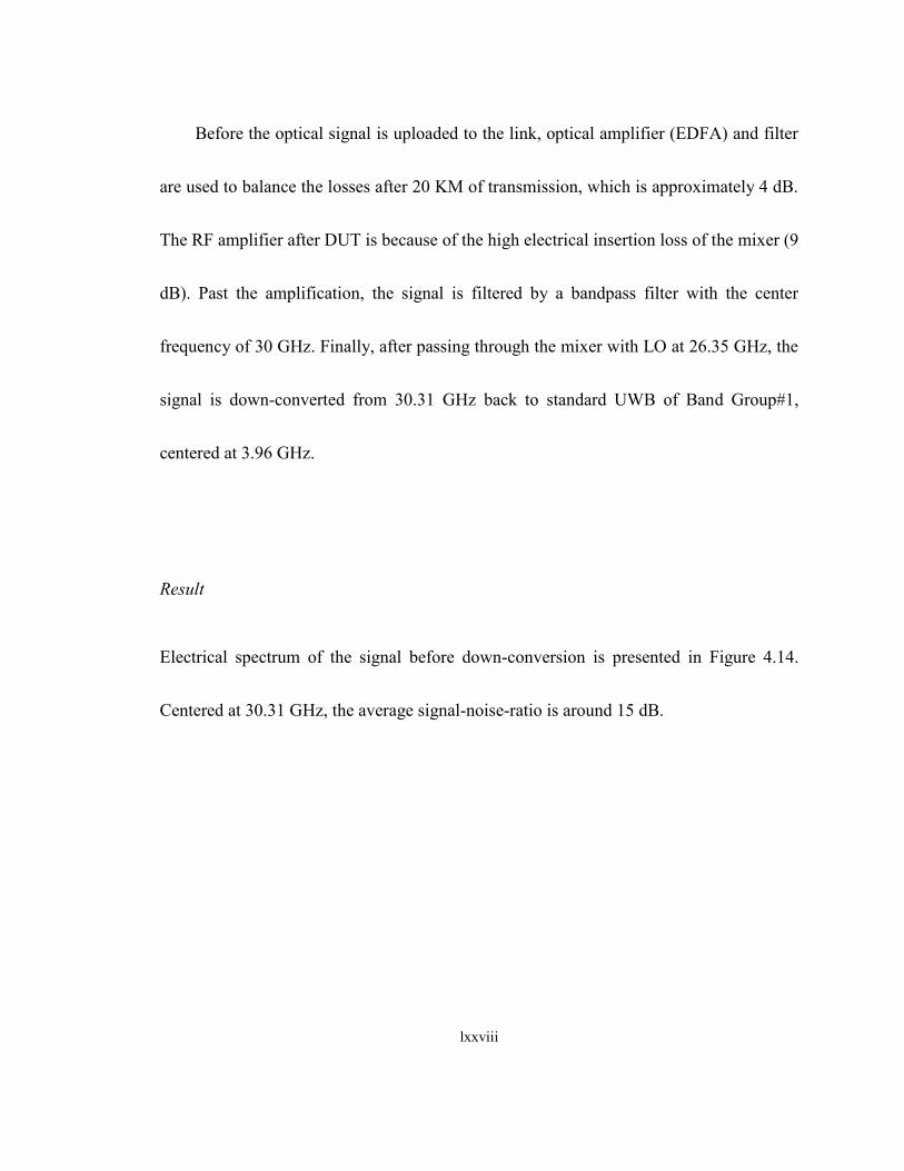
lxxviii
Before the optical signal is uploaded to the link, optical amplifier (EDFA) and filter
are used to balance the losses after 20 KM of transmission, which is approximately 4 dB.
The RF amplifier after DUT is because of the high electrical insertion loss of the mixer (9
dB). Past the amplification, the signal is filtered by a bandpass filter with the center
frequency of 30 GHz. Finally, after passing through the mixer with LO at 26.35 GHz, the
signal is down-converted from 30.31 GHz back to standard UWB of Band Group#1,
centered at 3.96 GHz.
Result
Electrical spectrum of the signal before down-conversion is presented in Figure 4.14.
Centered at 30.31 GHz, the average signal-noise-ratio is around 15 dB.
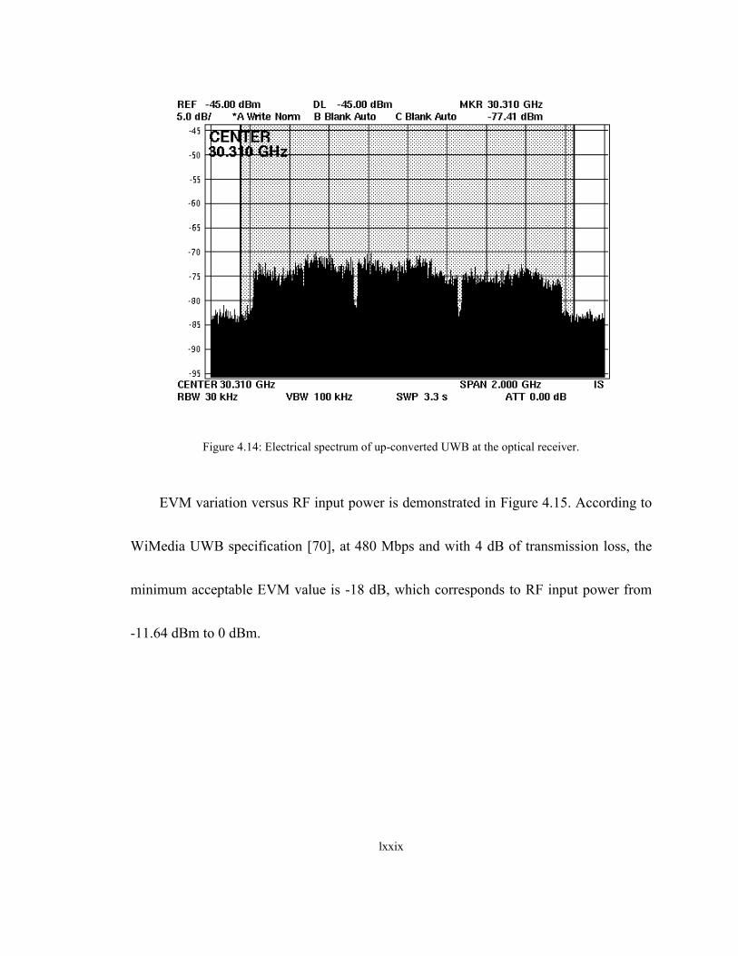
lxxix
Figure 4.14: Electrical spectrum of up-converted UWB at the optical receiver.
EVM variation versus RF input power is demonstrated in Figure 4.15. According to
WiMedia UWB specification [70], at 480 Mbps and with 4 dB of transmission loss, the
minimum acceptable EVM value is -18 dB, which corresponds to RF input power from
-11.64 dBm to 0 dBm.
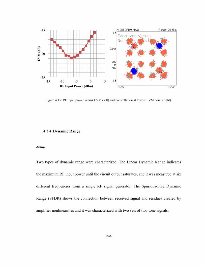
lxxx
Figure 4.15: RF input power versus EVM (left) and constellation at lowest EVM point (right).
4.3.4 Dynamic Range
Setup
Two types of dynamic range were characterized. The Linear Dynamic Range indicates
the maximum RF input power until the circuit output saturates, and it was measured at six
different frequencies from a single RF signal generator. The Spurious-Free Dynamic
Range (SFDR) shows the connection between received signal and residues created by
amplifier nonlinearities and it was characterized with two sets of two-tone signals.
-25
-20
-15
-15 -10 -5 0 5
EV
M (
dB
)
RF Input Power (dBm)
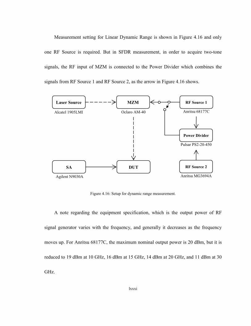
lxxxi
Measurement setting for Linear Dynamic Range is shown in Figure 4.16 and only
one RF Source is required. But in SFDR measurement, in order to acquire two-tone
signals, the RF input of MZM is connected to the Power Divider which combines the
signals from RF Source 1 and RF Source 2, as the arrow in Figure 4.16 shows.
Figure 4.16: Setup for dynamic range measurement.
A note regarding the equipment specification, which is the output power of RF
signal generator varies with the frequency, and generally it decreases as the frequency
moves up. For Anritsu 68177C, the maximum nominal output power is 20 dBm, but it is
reduced to 19 dBm at 10 GHz, 16 dBm at 15 GHz, 14 dBm at 20 GHz, and 11 dBm at 30
GHz.
Laser Source
Alcatel 1905LMI
MZM
Oclaro AM-40
DUT SA
Agilent N9030A
RF Source 1
Anritsu 68177C
RF Source 2
Anritsu MG3694A
Power Divider
Pulsar PS2-20-450
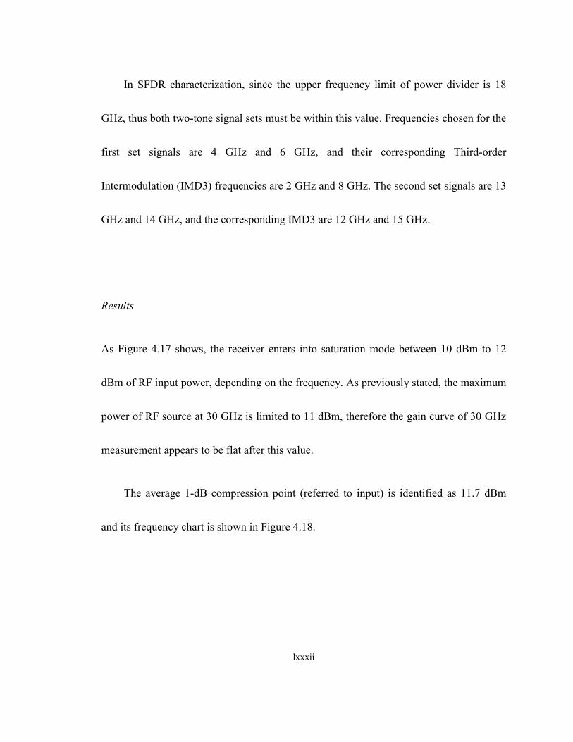
lxxxii
In SFDR characterization, since the upper frequency limit of power divider is 18
GHz, thus both two-tone signal sets must be within this value. Frequencies chosen for the
first set signals are 4 GHz and 6 GHz, and their corresponding Third-order
Intermodulation (IMD3) frequencies are 2 GHz and 8 GHz. The second set signals are 13
GHz and 14 GHz, and the corresponding IMD3 are 12 GHz and 15 GHz.
Results
As Figure 4.17 shows, the receiver enters into saturation mode between 10 dBm to 12
dBm of RF input power, depending on the frequency. As previously stated, the maximum
power of RF source at 30 GHz is limited to 11 dBm, therefore the gain curve of 30 GHz
measurement appears to be flat after this value.
The average 1-dB compression point (referred to input) is identified as 11.7 dBm
and its frequency chart is shown in Figure 4.18.

lxxxiii
Figure 4.17: RF input power versus output gain at different frequencies.
Figure 4.18: 1-dB compression point referred to RF input.
0
5
10
15
20
0 5 10 15 20
Ga
in (
dB
)
RF Input Power (dBm)
1 GHz
2.5 GHz
10 GHz
15 GHz
20 GHz
30 GHz
10
11
12
13
14
0 5 10 15 20 25 30
P1
dB
(d
Bm
)
Frequency (GHz)
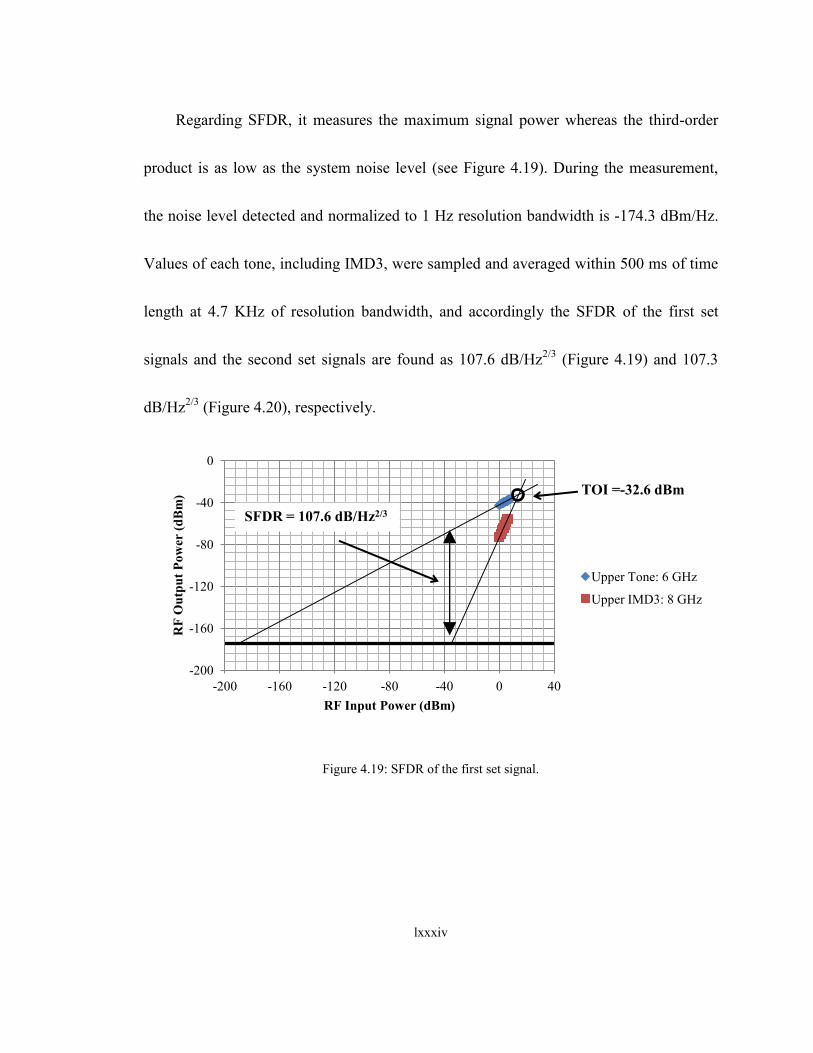
lxxxiv
Regarding SFDR, it measures the maximum signal power whereas the third-order
product is as low as the system noise level (see Figure 4.19). During the measurement,
the noise level detected and normalized to 1 Hz resolution bandwidth is -174.3 dBm/Hz.
Values of each tone, including IMD3, were sampled and averaged within 500 ms of time
length at 4.7 KHz of resolution bandwidth, and accordingly the SFDR of the first set
signals and the second set signals are found as 107.6 dB/Hz2/3
(Figure 4.19) and 107.3
dB/Hz2/3
(Figure 4.20), respectively.
Figure 4.19: SFDR of the first set signal.
-200
-160
-120
-80
-40
0
-200 -160 -120 -80 -40 0 40
RF
Ou
tpu
t P
ow
er (
dB
m)
RF Input Power (dBm)
Upper Tone: 6 GHz
Upper IMD3: 8 GHz
SFDR = 107.6 dB/Hz2/3
TOI =-32.6 dBm
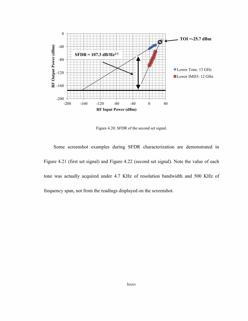
lxxxv
Figure 4.20: SFDR of the second set signal.
Some screenshot examples during SFDR characterization are demonstrated in
Figure 4.21 (first set signal) and Figure 4.22 (second set signal). Note the value of each
tone was actually acquired under 4.7 KHz of resolution bandwidth and 500 KHz of
frequency span, not from the readings displayed on the screenshot.
-200
-160
-120
-80
-40
0
-200 -160 -120 -80 -40 0 40
RF
Ou
tpu
t P
ow
er (
dB
m)
RF Input Power (dBm)
Lower Tone: 13 GHz
Lower IMD3: 12 GHz
SFDR = 107.3 dB/Hz2/3
TOI =-25.7 dBm
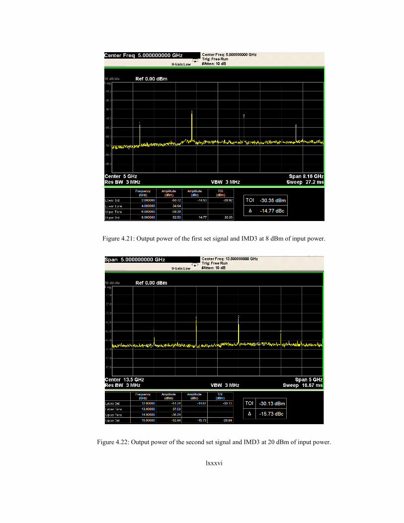
lxxxvi
Figure 4.21: Output power of the first set signal and IMD3 at 8 dBm of input power.
Figure 4.22: Output power of the second set signal and IMD3 at 20 dBm of input power.
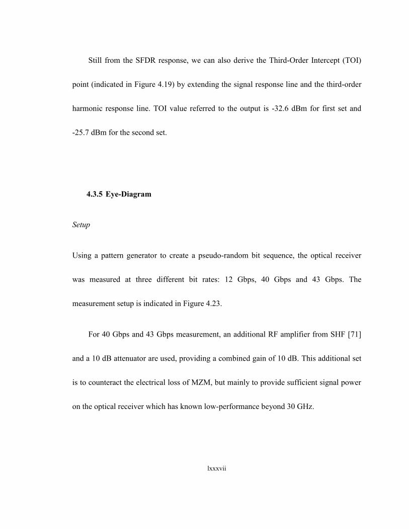
lxxxvii
Still from the SFDR response, we can also derive the Third-Order Intercept (TOI)
point (indicated in Figure 4.19) by extending the signal response line and the third-order
harmonic response line. TOI value referred to the output is -32.6 dBm for first set and
-25.7 dBm for the second set.
4.3.5 Eye-Diagram
Setup
Using a pattern generator to create a pseudo-random bit sequence, the optical receiver
was measured at three different bit rates: 12 Gbps, 40 Gbps and 43 Gbps. The
measurement setup is indicated in Figure 4.23.
For 40 Gbps and 43 Gbps measurement, an additional RF amplifier from SHF [71]
and a 10 dB attenuator are used, providing a combined gain of 10 dB. This additional set
is to counteract the electrical loss of MZM, but mainly to provide sufficient signal power
on the optical receiver which has known low-performance beyond 30 GHz.
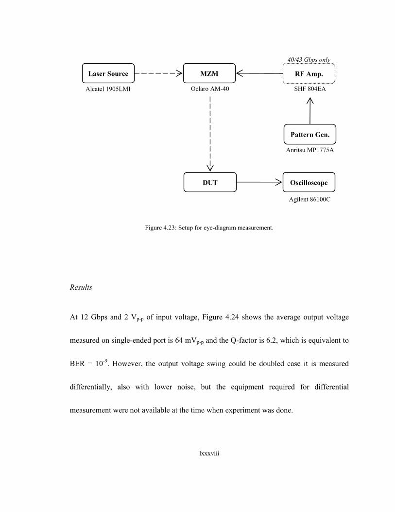
lxxxviii
Figure 4.23: Setup for eye-diagram measurement.
Results
At 12 Gbps and 2 Vp-p of input voltage, Figure 4.24 shows the average output voltage
measured on single-ended port is 64 mVp-p and the Q-factor is 6.2, which is equivalent to
BER = 10-9
. However, the output voltage swing could be doubled case it is measured
differentially, also with lower noise, but the equipment required for differential
measurement were not available at the time when experiment was done.
Laser Source
Alcatel 1905LMI
MZM
Oclaro AM-40
Pattern Gen.
Anritsu MP1775A
DUT Oscilloscope
Agilent 86100C
RF Amp.
SHF 804EA
40/43 Gbps only
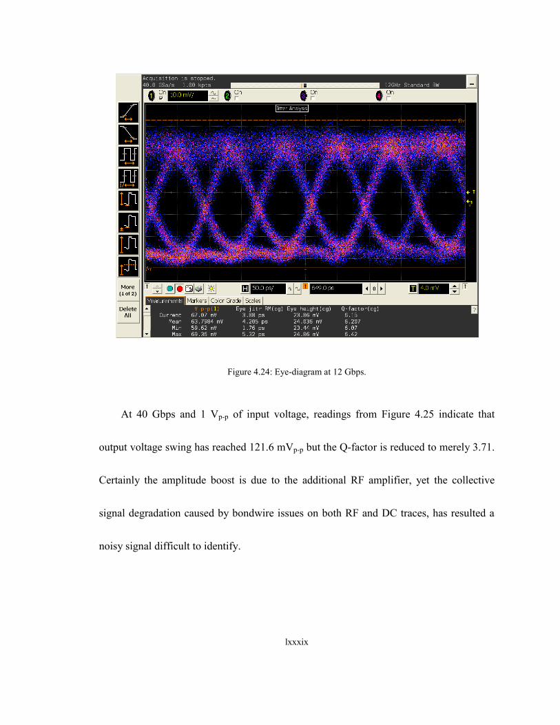
lxxxix
Figure 4.24: Eye-diagram at 12 Gbps.
At 40 Gbps and 1 Vp-p of input voltage, readings from Figure 4.25 indicate that
output voltage swing has reached 121.6 mVp-p but the Q-factor is reduced to merely 3.71.
Certainly the amplitude boost is due to the additional RF amplifier, yet the collective
signal degradation caused by bondwire issues on both RF and DC traces, has resulted a
noisy signal difficult to identify.
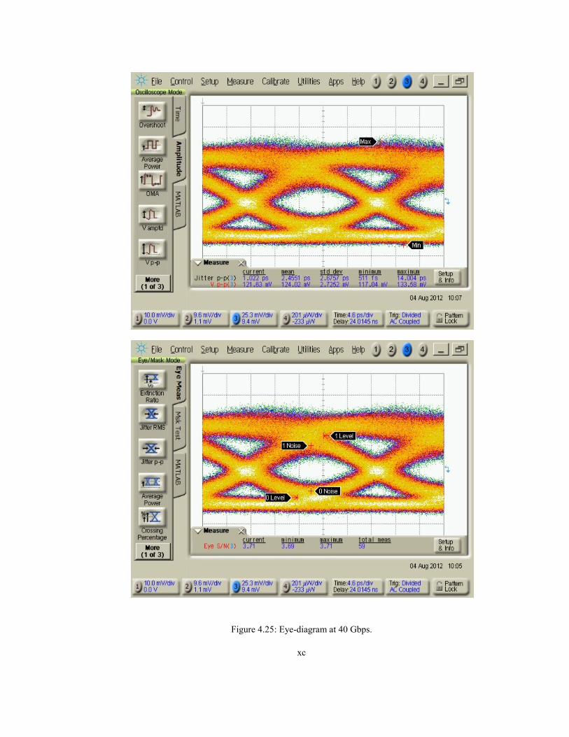
xc
Figure 4.25: Eye-diagram at 40 Gbps.
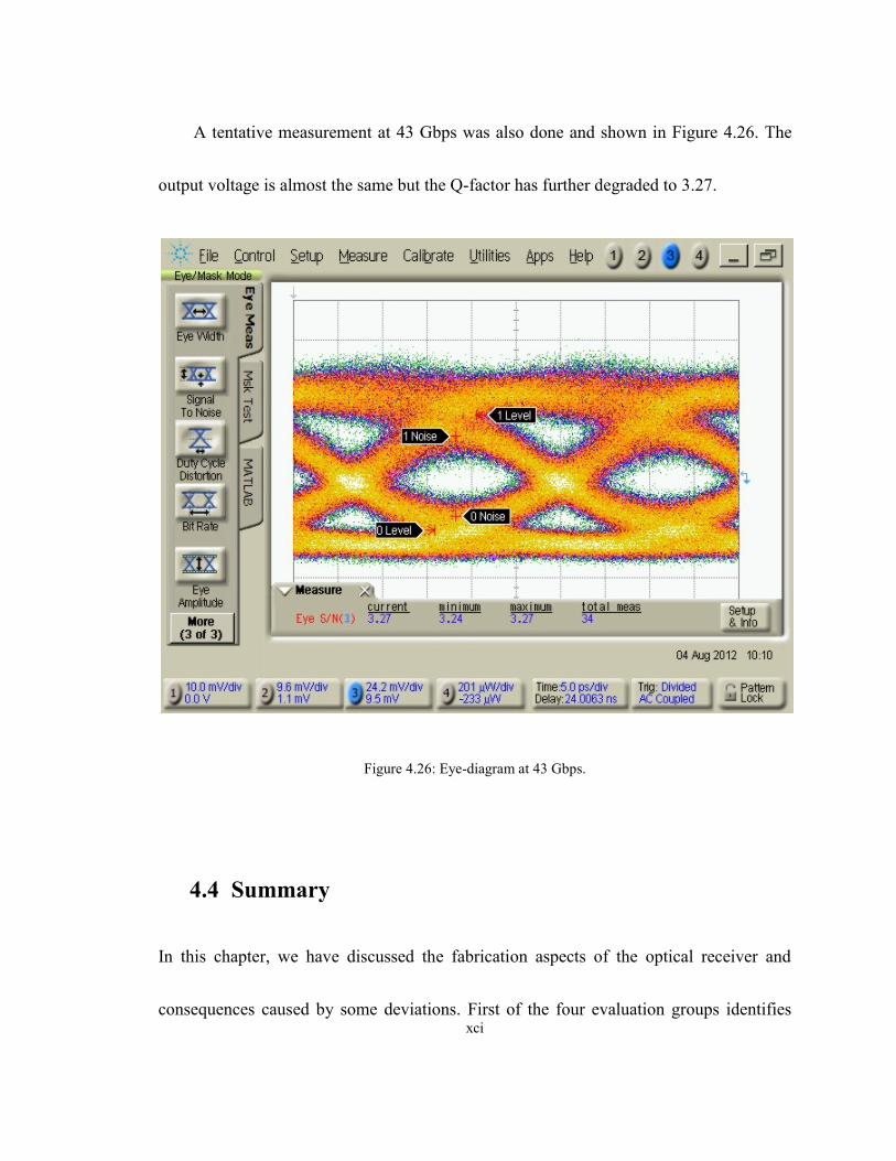
xci
A tentative measurement at 43 Gbps was also done and shown in Figure 4.26. The
output voltage is almost the same but the Q-factor has further degraded to 3.27.
Figure 4.26: Eye-diagram at 43 Gbps.
4.4 Summary
In this chapter, we have discussed the fabrication aspects of the optical receiver and
consequences caused by some deviations. First of the four evaluation groups identifies
xcii
the responsivity of optical receiver at 1550 nm is 0.325 A/W. Regarding frequency
evaluation, the transmission coefficient S21 has dropped significantly after 30 GHz and
basically the receiver bandwidth is regarded as this value. Bandwidth of 30 GHz is
further confirmed by the EVM evaluation, in which a UWB signal is transmitted at 30.31
GHz and processed by our optical receiver. In nonlinearity evaluation, the SFDR of two
sets of two-tone signals are found as 107.6 dB/Hz2/3
and 107.3 dB/Hz2/3
. Lastly, in
eye-diagram evaluation, the outcome of bondwire effects has also manifested on the
signal quality; the Q-factor measured at 12 Gbps is 6.2, equivalent to BER = 10-9
, but the
receiver has become noisy at 40 Gbps or above, resulting Q-factor no more than 3.7.
xciii
CHAPTER 5: CONCLUSION
5.1 Concluding Remarks
The primary goal of this thesis is to implement an ultra-broadband optical receiver for
RoF applications, aimed to cover frequency bands from 100 MHz to 50 GHz. The
receiver is built in hybrid integrated way which includes a lensed fiber, a photodetector
(PD), a transimpedance amplifier (TIA), two bias-tee circuits but later removed, and DC
bias circuit.
Unlike most optical receivers, we have used a lensed fiber to replace the
conventional fiber-lens method, leading to a much simpler coupling structure. Due to the
MFD mismatch between PD and lensed fiber, it is expected to have certain coupling loss
even perfect alignment is achieved. Once the optical signal is converted into electrical,
the TIA provides current-to-voltage conversion as well as signal amplification. Also,
there is a specific demand from TIA which requires bias-tee circuit on each output trace,
and this circuit is accomplished with discrete RF components.
Two issues that may impact the receiver performance are mentioned during the
design process and simulation, and then verified once the circuit is fabricated. The first
problem relates to the optical coupling loss. Loss introduced by MFD mismatch is
xciv
already known, but the final result still depends on the alignment precision between fiber
and PD. Measurement has shown the total optical coupling loss is -3.91 dB, partly
contributed by the epoxy because it has caused the fiber to shift before it being solidified.
The second problem involves the bondwires, since their transmission line effects at high
frequencies could be significant. For RF signal connections, bondwires were simulated
and the result shown they could degrade the overall bandwidth to 26.7 GHz in the worst
case. However, this result does not include the effect of bondwire on DC traces, because
insufficient bondwires and lengthy connections will add noise to the circuit.
During the back-to-back characterization of optical receiver, average 1-dB
compression point sampled at different frequencies is found as 11.7 dBm (referred to
input), and the average SFDR based on two sets of two-tone frequencies (4 GHz with 6
GHz, and 13 GHz with 14 GHz) is 107.45 dB/Hz2/3
. Bandwidth of the optical receiver is
identified from S-parameter and EVM measurement, with proven performance of 30 GHz
bandwidth. However, due to bondwire effects, operation at 43 Gbps is too noisy
according to industrial standards. Therefore, refinement of bondwire implementing
method or alternative interconnect solution is expected to be the next step for
advancement works. Regarding the optical-to-electrical conversion rate, the receiver
xcv
responsivity is found as 0.325 A/W at 1550 nm, which is lower than the nominal PD
value 0.8 A/W, because of the MFD mismatch and fiber alignment precision, as stated
earlier. This result also points out another possible direction for future work, involving
the coupling technique of optical components.
5.2 Future Work
Future works of this thesis can be categorized into three subjects: signal quality, optical
coupling technique, and functional upgrades.
Signal Quality
The issue of signal quality starts with the optical insertion loss caused by MFD mismatch.
Lensed fiber with smaller MFD is achievable but it was simply unavailable from all
companies inquired at the time of circuit fabrication. At least 1 dB of optical loss could
be removed if the MFD of lensed fiber and PD are totally matched.
On the electrical side, bondwire is certainly the main problem. Accurate and short
bondwire is practicable with higher precision facilities, but unless precise bondwire can

xcvi
be assured, otherwise flip-chip mounting will be the best solution to avoid signal
degradation.
Optical Coupling Technique
The fiber installation process is an interesting subject to be reviewed. In fact, processing
details are typically regarded as business confidential, and each company has developed
its own technology for maximum coupling efficiency and streamline assembly process.
According to a generic report, the use of metalized lensed fiber plus laser welding
technique could provide higher-accuracy and more robust attachment comparing to the
epoxy that we have used, but it still require further studies to reveal the details. In this
work, at least 2.9 dB of optical insertion loss was caused by the fiber-drift after applying
the epoxy.
Another topic under this subject is the alignment method. Automatic fiber alignment
process would be an interesting target, because conventional methods are inefficient and
costly. The basic principle of fiber alignment is to find the best position in
three-dimensional space in which the photodetector produces maximum current. It has
been reported in [72] the use of dynamic comb-drive actuators integrated in front of the

xcvii
photodetector receptacle, with a control circuit that adjusts the comb-drive position
basing on PD output current, the alignment process is almost automatically completed.
But this integration of comb-drive actuators still has some technical difficulties and
compatibility issues with the fabrication process, thus structural simplification and less
dependent to the fabrication process could be a potential solution to be investigated.
Functional Upgrade
Upgrading the receiver into balanced-photodiode structure will expand its functionality
and performance, because this structure will lead to better optical sensitivity, higher
dynamic range, and lower noise.
xcviii
BIBLIOGRAPHY
[1] U.S. Department of Commerce, "United States Frequency Allocations," Oct 2003.
[Online]. Available:
http://www.ntia.doc.gov/files/ntia/publications/2003-allochrt.pdf. [Accessed Sep
2012].
[2] H. Al-Raweshidy and S. Komaki, Radio over Fiber Technologies for Mobile
Communications Networks, Artech House, 2002.
[3] N. Anscombe, "Demand for indoor coverage drives radio-over-fibre, wireless
europe," Feb/Mar 2005. [Online]. Available:
http://www.nadya-anscombe.com/downloadlibrary/radio%20over%20fibre.pdf.
[Accessed 17 Sep 2012].
[4] A. K. Dutta, M. Takechi, R. S. Virk, M. Kobayashi, K. Araki, K. Sata, M. Gentrup
and R. Ragle, "40 Gb/s Postamplifier and PIN/Preamplifier Modules for Next
Generation Optical Front-End System," Journal of Lightwave Technology, Vol.20,
No.12, pp. 2229-2238, December 2002.
[5] Y.-H. Kwon, J.-S. Choe, J. Kim, K. Kim, K.-S. Choi, B.-S. Choi and H.-G. Yun,
"Fabrication of 40 Gb/s Front-End Optical Receivers Using Spot-Size Converter
Integrated Waveguide Photodiodes," ETRI Journal, Volume 27, Number 5, pp.
484-489, October 2005.
[6] SHF Communication Technologies AG, "Datasheet: SHF 47100 A, O/E
Conversion Module," [Online]. Available:
http://www.shf.de/fileadmin/download/47100a.pdf. [Accessed 2 2012].
xcix
[7] F. Y. Xu, "High Precision Adhesives for Free Space Micro-Optics Applications,"
in Electronic Components and Technology Conference, 2003.
[8] H. Tsunetsugu, K. Katsura, T. Hayashi, F. Ishitsuka and S. Hata, "A New
Packaging Technology Using Microsolfer Bumps for High-Speed Photoreceivers,"
IEEE Transactions on Components, Hybrids, and Manufacturing Technology, Vol.
15, No. 4, pp. 578-582, 1992.
[9] J. H. Song, H. N. J. Fernando, B. Roycroft, B. Corbett and F. H. Peters, "Practical
Design of Lensed Fibers for Semiconductor Laser Packaging Using Laser Welding
Technique," Journal of Lightwave Technology, Vol. 27, No. 11, pp. 1533-1538, 1
June 2009.
[10] J. Chandrappan, Z. Jing, R. V. Mohan, P. O. Gomez, T. A. Aung, Y. Xiao, P. V.
Ramana, J. H. Lau and D. L. Kwong, "Optical Coupling Methods for
Cost-Effective Polymer Optical Fiber Communication," IEEE Transactions on
Components and Packaging Technologies, Vol. 32, No. 3, pp. 593-599, September
2009.
[11] Corning Incorporated, "Mode-Field Diameter, Measurement Method," August
2001. [Online]. Available:
http://www.corning.com/docs/opticalfiber/mm16_08-01.pdf. [Accessed February
2012].
[12] J. D. Gibson, "Fiber Optic Connectors and Splices," in The Communications
Handbook, 2nd Edition, CRC Press, 2002, pp. 49-4, 49-5.
[13] D. Wake, T. P. Spooner, S. D. Perrin and I. D. Henning, "50 GHz InGaAs
Edge-Coupled pin Photodetector," Electronics Letters, Vol. 27, No. 12, pp.
1073-1075, June 1991.
[14] K. Kato, S. Hata, K. Kawano, J. Yoshida and A. Kozen, "High-Efficieny 50 GHz
c
InGaAs Multimode Waveguide Photodetector," IEEE Journal of Quantum
Electronics, Vol. 28, Issue 12, pp. 2728-2735, Dec 1992.
[15] E. Sackinger, "P-I-N Photodetector," in Broadband Circuits for Optical Fiber
Communication, John Wiley & Sons, 2005, pp. 26-27.
[16] J. E. Bowers and J. C. A. Burrus, "Ultrawide-Band Long-Wavelength p-i-n
Photodetectors," Journal of Lightwave Technologies, Vol. 5, Issue 10, pp.
1339-1350, October 1987.
[17] Archcom Technology Inc., "AC6180-C 40 Gbps Waveguide InP Photodetector,"
Archcom Technology Inc., Azusa, CA, USA.
[18] A. S. Sedra and K. C. Smith, "Feedback," in Microelectronic Circuits, Oxford
Press, 2010, pp. 804-890.
[19] E. Sackinger, "Shunt Feedback TIA," in Broadband Circuits for Optical Fiber
Communication, John Wiley & Sons, 2005, pp. 113-121.
[20] Inphi Corporation, "4335TA - Inphi," [Online]. Available:
http://www.inphi.com/products-technology/networking-communications-products/
transimpedance-amplifiers/4335ta.php. [Accessed 7 2011].
[21] TriQuint Semiconductor, "TGA4812: 40G Transimpedance Amplifier," TriQuint
Semiconductor, May 2009.
[22] RFMD, "SFT-9200B: 50 GHz Transimpedance Amplifier," [Online]. Available:
http://www.rfmd.com/CS/Documents/SFT-9200BDS.pdf. [Accessed 4 Sep 2012].
[23] GTRAN, "GTRAN 43 Gbps Transimpedance Amplifier: GT40-5015TA,"
GTRAN, Camarillo, CA, USA, 2010.
[24] Texas Instruments, "Interfacing Between LVPECL, VML, CML, and LVDS

ci
Levels," December 2002. [Online]. Available:
http://www.ti.com/lit/an/slla120/slla120.pdf. [Accessed 19 April 2012].
[25] R. H. Caverly, "Characteristic Impedance of Integrated Circuit Bond Wires," in
IEEE Trans. Microwave Theory Tech., Vol. 34, pp. 982-984, 1986.
[26] F. Alimenti, U. Goebel and R. Sorrentino, "Quasi Static Analysis of Microstrip
Bondwire Interconnections," in Proc. IEEE MTT-Symp, pp. 679-682, Orlando, FL,
1995.
[27] T. Krems, W. Haydl, L. Verweyen, M. Schlechtweg, H. Massler and J. Rudiger,
"Coplanar Bond Wire Interconnections for Millimeterwave Applications," in
Electrical Performance of Electronic Packaging, pp. 178-180, 1995.
[28] A. Sutono, N. G. Cafaro, J. Laskar and E. Tentzeris, "Experimental Study and
Modeling of Microwave Bond Wire Interconnects," in IEEE Antennas and
Propagation Society International Symposium, Vol. 4, pp. 2020-2023, Atlanta,
GA, 2000.
[29] T. Krems, W. Haydl, H. Massler and J. Rudiger, "Millimeter-wave Performance of
Chip Interconnections Using Wire Bonding and Flip Chip," in IEEE MTT-S
Microwave Symposium Digest, Vol. 1, pp. 247-250, 1996.
[30] K. Mouthaan, "Microwave Modeling and Measurement of the Self- and Mutual
Inductance of Coupled Bondwires," in Bipolar/BiCMOS Circuits and Technology
Meeting, pp. 166-169, 1997.
[31] A. O. Harm, K. Mouthaan, E. Aziz and M. Versleijen, "Modeling and Simulation
of Hybrid RF Circtuis Using a Versatile Compact Bondwire Model," in 28th
European Microwave Conference, Vol. 2, pp. 529-534, 1998.
[32] T. P. Budka, "Wide-Bandwidth Millimeter-Wave Bond-Wire Interconnects," IEEE
cii
Transactions on Microwave Theory and Techniques, pp. 715-718, Apr 2001.
[33] Y. Miyamoto, M. Yoneyama, Y. Imai, K. Kato and H. Tsunetsugu, "40 Gbit/s
Optical Receiver Module Using a Flip-Chip Bonding Technique for Device
Interconnection," Electronics Letters, Vol. 34, Issue 5, pp. 493-494, 5 May 1998.
[34] E. Camargo, R. S. Virk, R. Haiji, S. Parker, S. Notomi and H. Ohnishi, "Design of
broadband amplifier for high speed applications," in European Microwave
Conference, 2002.
[35] I. Wolff, Coplanar Microwave Integrated Circuits, John Wiley & Sons, 2006.
[36] R. N. Simons, Coplanar Waveguide Circuits, Components, and Systems, John
Wiley & Sons, 2001.
[37] S. Marsh, Practical MMIC Design, Artech House, 2006.
[38] M. Houdart, "Coplanar Lines: Application to Lumped and Semi-Lumped
Microwave Integrated Circuits," in 7th European Microwave Conference,
pp.450-454, 1977.
[39] R. Sorrentino and G. Bianchi, "Basic MMIC elements," in Microwave and RF
Engineering, John Wiley & Sons, 2010, pp. 640-641.
[40] T. Becks and I. Wolff, "Full-Wave Analysis of Various Coplanar Bends and
T-Juntions with Respect to Different Types of Air-Bridges," in Microwave
Symposium Digest, Vol.2, pp.697-700, 1993.
[41] H. Kim and R. Franklin-Drayton, "Wire-Bond Free Technique for Right-Angle
Coplanar Waveguide Bend Structures," IEEE Transactions on Microwave Theory
and Techniques, Vol.57, No. 2, pp. 442-448, February 2009.
[42] K. C. Gupta, R. Garg, I. Bahl and P. Bhartia, "Microstrip Applications," in
ciii
Microstrip Lines and Slotlines, Artech House, 1996, pp. 122-152.
[43] B. C. Wadell, "Inductors & Capacitors," in Transmission Line Design Handbook,
Artech House, 1991, pp. 379-431.
[44] I. Wolff, "Coplanar Lumped Elements," in Coplanar Microwave Integrated
Circuits, John Wiley & Sons, 2006, pp. 249-304.
[45] Poly-GRAMES Research Center, "RF Circuit Fabrication Rules," [Online].
Available: http://132.207.65.61/pcb-process/RF_circuit_fabrication_rules.pdf.
[Accessed Feb 2012].
[46] "Bias Network," in Practical Microstrip Design and Applications, Artech House,
2005, pp. 288-291.
[47] R. K. Joshi, "Characteristics of a Rotated Butterfly Radial Stub," in Microwave
Symposium Digest, IEEE MTT-S, pp.1165-1168, 2006.
[48] M. S. Razalli, "Compact "Butterfly" Microwave Ultra-Wideband Filter," in
Asia-Pacific Conference on Applied Electromagnetics, pp.1-5, 2007.
[49] D. Zhihong, "A 40GHz Amplifier Design Using CPW," in International
Symposium on Electromagnetic Compatibility, pp.337-340, 2007.
[50] K.-S. Choi, Y.-H. Kwon, J.-S. Choe, Y.-D. Chung, Y.-S. Kang, J. Kim, B.-T. Ahn
and J.-T. Moon, "Development of Packaging Technologies for High-Speed
(>40Gb/s) Optical Modules," IEEE Journal of Selected Topics in Quantum
Electronics, Vol.12, Issue 5, pp. 1017-1024, 2006.
[51] H.-G. Yun, K.-S. Choi, Y.-H. Kwon, J.-S. Choe and J.-T. Moon, "Integration and
Characteristics of 40-Gb/s Electroabsorption Modulator Integrated Laser Module
with a Driver Amplifier and Bias Tees," IEEE Transactions on Advanced
civ
Packaging, Vol.31, Issue 4, pp. 855-860, Nov 2008.
[52] R. N. Simons, "Coplanar Waveguide Spiral Inductor," in Coplanar Waveguide
Circuits, Components, and Systems, John Wiley & Sons, 2001, pp. 262-266.
[53] I. Wolff, "The Coplanar Spiral Inductor," in Coplanar Microwave Integrated
Circuits, John Wiley & Sons, 2006, pp. 276-295.
[54] N. Kinayman and M. I. Aksun, "Microwave Lumped Elements," in Modern
Microwave Circuits, Artech House, 2005, pp. 533-544.
[55] N. Masoumi, S. Safavi-Naeini and M. Elmasry, "An Efficient and Accurate Model
for RF/Microwave Spiral Inductors Using Microstrip Lines Theory," in
International Conference on Computer Design, pp.127-132, 2000.
[56] J. Y. Hasani, M. Kamarei and F. Ndagijimana, "Inductor Design and Optimization
for Millimeter Wave Integrated Circuit Applications," in IEEE 18th International
Symposium on Personal, Indoor and Mobile Radio Communications, pp.1-4, 2007.
[57] J. Brinkhoff, K. Koh, K. Kang and F. Lin, "Scalable Transmission Line and
Inductor Models for CMOS Millimeter-Wave Design," in IEEE Transactions on
Microwave Theory and Techniques, Vol. 56, Issue 12, pp.2954-2962, 2008.
[58] D. Dubuc, T. Tournier, I. Telliez, T. Parra, C. Boulanger and J. Graffeuil, "High
Quality Factor and High Self-Resonant Frequency Monolithic Inductor for
Millimeter-Wave Si-based IC's," in IEEE MTT-S International Microwave
Symposium Digest, Vol.1, pp.193-196, 2002.
[59] J. Shi, K. Kang, Y. Z. Xiong, J. Brinkoff, F. Lin and X.-J. Yuan,
"Millimeter-Wave Passives in 45-nm Digital CMOS," IEEE Electron Device
Letters, Vol. 31, Issue 10, pp. 1080-1082, 2010.

cv
[60] C.-Y. Chi and G. M. Rebeiz, "Planar millimeter-wave microstrip lumped elements
using micro-machining techniques," in IEEE MTT-S, International Microwave
Symposium Digest, Vol.2, pp.657-660, 1994.
[61] Coilcraft Inc., "Coilcraft: Rugged, Surface Mount Broadband Conical Inductors,"
[Online]. Available: http://www.coilcraft.com/pdfs/bcr.pdf. [Accessed May 2012].
[62] AVX Corporation, "AVX: GX02 Series FFVS Data Sheet," [Online]. Available:
www.avx.com/docs/catalogs/gx.pdf. [Accessed May 2012].
[63] H. Patterson, "Analysis of ground bond wire arrays for RFICs," in IEEE MTT-S
International Microwave Symposium Digest, Tempe, AZ, 1997.
[64] SHF Communication Technologies AG, "Precision Coaxial Connectors," [Online].
Available:
http://www.shf.de/fileadmin/download/Connectors_and_Cables/kmco_complete_v
004.pdf. [Accessed 19 June 2012].
[65] Coorstek Inc., "Thin Film Substrates," [Online]. Available:
http://www.coorstek.com/resources/8510-1164ThinFilm.pdf. [Accessed 29 June
2012].
[66] Picosecond Pulse Labs, "Bias Tees: Model 5542," [Online]. Available:
http://www.picosecond.com/product/product.asp?prod_id=27. [Accessed 7 Aug
2012].
[67] u2t Photonics AG, "XPDV4120R," [Online]. Available:
http://www.u2t.com/index.php/products/photodetectors/item/xpdv4120r?category_
id=2. [Accessed 8 Aug 2012].
[68] Alcatel Optronics, "Alcatel 1905 LMI," 2002. [Online]. Available:
http://pdf.dzsc.com/autoupload/230600db-8d02-444f-b336-ca659ebba386.pdf.
cvi
[Accessed 5 Aug 2012].
[69] Oclaro, "PowerLog AM-40," 2009. [Online]. Available:
http://www.oclaro.com/datasheets/Oclaro_PowerLog_AM2040_v1_1.pdf.
[Accessed 5 Aug 2012].
[70] WiMedia Alliance, "WiMedia SER PHY Specification," WiMedia Alliance, 2005.
[71] SHF Communication Technologies AG, "Datasheet: SHF 804 EA Broadband
Amplifier," 24 Mar 2004. [Online]. Available:
http://www.shf.de/fileadmin/download/804ea.pdf. [Accessed 11 Sep 2012].
[72] B. Morgan, J. McGee and R. Ghodssi, "Automated Two-Axes Optical Fiber
Alignment Using Grayscale Technology," Journal of Microelectromechanical
Systems, Vol. 16, No. 1, pp. 102-110, Feb 2007.