htg-v6hxt-x16pcie user manual - xilinx · htg-v6hxt-x16pcie user manual 7 2.3) fpga bank assignment...
TRANSCRIPT

HTG-V6HXT-X16PCIE User Manual
www.HiTechGlobal.com
1
HiTech Global Virtex-6HXT X16 PCI Express Ethernet Networking Development Platform
HTG-V6HXT-X16PCIE User Manual
Version 1.1 June 2011
Copyright © HiTech Global 2002-2011

HTG-V6HXT-X16PCIE User Manual
www.HiTechGlobal.com
2
Disclaimer
HiTech Global does not assume any liability arising out of the application or use of any product described or shown herein; nor does it convey any license under its patents, copyrights, or mask work rights or any rights of others. HiTech Global reserves the right to make changes, at any time, in order to improve reliability and functionality of this product. HiTech Global will not assume responsibility for the use of any circuitry described herein other than circuitry entirely embodied in its products. HiTech Global provides any design, code, or information shown or described herein "as is." By providing the design, code, or information as one possible implementation of a feature, application, or standard, HiTech Global makes no representation that such implementation is free from any claims of infringement. End users are responsible for obtaining any rights they may require for their implementation. HiTech Global expressly disclaims any warranty whatsoever with respect to the adequacy of any such implementation, including but not limited to any warranties or representations that the implementation is free from claims of infringement, as well as any implied warranties of merchantability or fitness for a particular purpose.
HiTech Global will not assume any liability for the accuracy or correctness of any engineering or software support or assistance provided to a user. HiTech Global products are not intended for use in life support appliances, devices, or systems. Use of a HiTech Global product in such applications without the written consent of the appropriate HiTech Global officer is prohibited. The contents of this manual are owned and copyrighted by HiTech Global Copyright 2002-2007 HiTech Global All Rights Reserved. Except as stated herein, none of the material may be copied, reproduced, distributed, republished, downloaded, displayed, posted, or transmitted in any form or by any means including, but not limited to, electronic, mechanical, photocopying, recording, or otherwise, without the prior written consent of HiTech Global. Any unauthorized use of any material contained in this manual may violate copyright laws, trademark laws, the laws of privacy and publicity, and communications regulations and statutes. Revision History
Date Version Notes 5/15/2011 1.0 Preliminary 6/1/2011 1.1

HTG-V6HXT-X16PCIE User Manual
www.HiTechGlobal.com
3
Table Of Contents
Chapter 1 - Introduction to Virtex-6 HXT 4 1.1) Summary of Virtex-6 HXT FPGA Features 4 1.2) Virtex-6 HXT Family Serial I/O Protocol Support 4 Chapter 2 – Development Platform Introduction 6 2.1) Introduction 6 2.2) Features & Block Diagram 6 2.3) FPGA Bank Assignment 7 2.4) Clock Distribution 8 2.5) PCI Express 9 2.6) DDR III Memory 12 2.7) QDR-II Interface 18 2.8) 10G/40F SFP+/QSFP+ Interfaces 21 2.8.1) QSFP+ port with EDC and CDR support 21 2.8.2) QSFP+ port with direct FPGA interface 24 2.8.3) SFP+ ports with direct FPGA interface 25 2.9) FPGA Mezzanine Card Interfaces 26 2.9.1) FMC “A” (11.18Gbps) 27 2.9.2) FMC “A” (6.6Gbps) 34 2.10) USB To UART Bridge 39 2.11) LEDs, GPIO Headers & Pushbuttons 40 2.12) Configuration 42 Chapter 3 – FMC Modules

HTG-V6HXT-X16PCIE User Manual
www.HiTechGlobal.com
4
Chapter 1: Introduction to Xilinx Virtex-6 HXT 1.1) Overview
The Virtex®-6 FPGAs are the programmable silicon foundation for Targeted Design Platforms that deliver integrated software and hardware components to enable designers to focus on innovation as soon as their development cycle begins. Optimized for applications that require ultra high-speed serial connectivity, Virtex®-6 HXT FPGAs offer the industry’s highest serial bandwidth through a combination of 6.6Gbps GTX transceivers and 11.18Gbps GTH transceivers to enable next-generation packet and transport, switch fabric, video switching, and imaging equipment.
Table (1) illustrates key features of the Virtex-6 HXT family.
Features HXT380/HX565 40nm ExpressFabric™ architecture with 6-input LUTs 600MHz clock management tiles (2 MMCM) 18
600MHz block RAM (1,000Kbits) 18.1 - 32.8 1.40Gbps SelectIO™ with ChipSync™ technology 6.6Gbps GTX transceivers 48 11.18Gbps GTH transceivers 24 PCI Express ( PCIe ) Endpoint/Root Port blocks 4 Ethernet Media Access Controller blocks 4 600MHz DSP48E1 slices 864 System monitor and analog-to-digital converter Third-generation sparse chevron packaging technology Enhanced configuration and bitstream protection
Table (1) Summary of Virtex-6 HXT FPGA Features
1.2) Virtex-6 HXT Family Serial I/O Protocol Support GTX (6.6Gbps) and GTH (11.18Gbps) serial transceivers of the Virtex-6 HXT devices support different ranges of serial protocol standards. Table (2) illustrates these supported standards and protocols.
Serial I/O Protocol Line Rate (Gbps) Transceiver Type PCI-Express® 5.0, 2.5 GTX
XAUI 3.125 GTX 10G Ethernet 10.3125 GTH OIF CEI-6G 6.25 GTX Interlaken 4.976, 6.25 GTX
Gigabit Ethernet 1.25 GTX Hi-Gig 6.5625, 3.75 GTX
OC-192 9.953 GTH OC-48 2.488 GTX OC-12 0.622 GTX OC-3 0.155 GTX
OTU-1 2.677 GTX OTU2 10.7 GTH

HTG-V6HXT-X16PCIE User Manual
www.HiTechGlobal.com
5
OUT-4 11.18 GTH Serial RapidIO 6.25, 3.125 GTX
CPRI 9G 9.8 GTH CPRI 0.614, 1.228, 2.457, 3.072, 4.912, 6,144 GTX
OBSAI 0.768, 1.536, 3.072 GTX HD-SDI 1.485 GTX 3G SDI 2.97 GTX
DisplayPort 2.7 GTX Serial ATA 6.0, 3.0, 1.5 GTX
Fibre Channel 4.25, 2.0625, 1.0625 GTX SAS 6.0, 3.0, 1.5 GTX
Infiniband 2.5 GTX GPON 1.244 GTX
10G BASE KR 10.3125 GTH CEI-11 11.1 GTH SFP+ 10.3125 GTH
Table (2) Virtex-6 HXT Supported Serial Protocols

HTG-V6HXT-X16PCIE User Manual
www.HiTechGlobal.com
6
Chapter 2:Development Platform Introduction
◙ 2.1) Introduction
Powered by Xilinx Virtex-6 HX380T or HX565T FPGA, the X16-PCIE Ethernet network card provides access to sixteen lanes of PCI Express Gen 2 (64 Gbps raw data throughput), ten SFP+ optical connectors (100 Gbps), up to 16 GB of DDR3 SO-DIMM, QDR II, ten 11.18 Gbps and ten 6.6Gbps serial ports. The on-board FPGA Mezzanine Connectors (FMC) along with off-the-shelf FMC modules, expend the functionality of the board for variety of different applications
◙ 2.2) Features
▪ Xilinx HX380T or HX565T FPGA ▪ X16 PCI Express Edge Connector ▪ X1 QSFP+ port with EDC support through external PHY chips ▪ X1 QSFP+ port with direct interface to the on-board FPGA's GTH (10G) serial transceivers ▪ X2 SFP+ ports with direct interface to the on-board FPGA's GTH (10G) serial transceivers ▪ X2 DDR-3 SODIMM ▪ X3 QDR-II Components ▪ X1 SMA Port (10G) ▪ X2 FPGA Mezzanine Connectors (FMC) - FMC #B: 34 LVDS IOs and 10 GTX (6.6 Gbps) Serial IOs - FMC #A: 9 LVDS IOs and 10 GTH (11.18 Gbps) Serial IOs ▪ Configuration through JTAG , Micron G18 flash, or CPLD+ Xilinx Flash ▪ USB to UART ▪ ATX and DC power supplies for PCI Express and stand alone operations ▪ LEDs & Pushbuttons ▪ Size: 9.5" x 4.25"
Figure (1) Block Diagram & Placement

HTG-V6HXT-X16PCIE User Manual
www.HiTechGlobal.com
7
◙ 2.3) FPGA Bank Assignment
Common footprint of the HX380T and HX565T in FFG1923 package allows usage of one PCB for both devices. FPGA bank allocation for each interface is illustrated by figure (2).
Figure (2): FPGA Bank Assignment

HTG-V6HXT-X16PCIE User Manual
www.HiTechGlobal.com
8
◙ 2.4) Clock Distribution For effective utilization of the FPGA resources, the HTG-V6HXT-X16PCIE board is supported by different low-jitter crystal oscillators. Figure (3) illustrates the entire board’s clock diagram.
Figure (3): Clock Diagram

HTG-V6HXT-X16PCIE User Manual
www.HiTechGlobal.com
9
◙ 2.5) PCI Express The HTG-V6HXT-X16PCIE provides 16 lanes of PCI Express Gen2 interface (16x5Gbps) through two FPGA embedded PCI Express controllers and one PLX (part number PEX8632) external switch as shown by figure (4).
Figure (4): PCI Express Gen 2 Switch Diagram
The interface provides data throughput of approximately about 64Gbps from a host PC to the FPGA and vice versa. The lane configuration is selected through setting of the J8 jumper header. The factory default setting is for the x16 configuration. Table (3) illustrates FPGA pins assignment for PCI Express signals.
PCI Express Signal Name FPGA Signal Name FPGA Pin # PEX_TX[15]_P MGTTXP0_112 AN3 PEX_TX[15]_N MGTTXN0_112 AN4 PEX_TX[14]_P MGTTXP1_112 AM1 PEX_TX[14]_N MGTTXN1_112 AM2 PEX_TX[13]_P MGTTXP2_112 A3 PEX_TX[13]_N MGTTXN2_112 A4 PEX_TX[12]_P MGTTXP3_112 AK1 PEX_TX[12]_N MGTTXN3_112 AK2
PEX_RX[15]_P MGTRXP0_112 AL7 PEX_RX[15]_N MGTRXN0_112 AL8 PEX_RX[14]_P MGTRXP1_112 AM5 PEX_RX[14]_N MGTRXN1_112 AM6 PEX_RX[13]_P MGTRXP2_112 AJ7 PEX_RX[13]_N MGTRXN2_112 AJ8 PEX_RX[12]_P MGTRXP3_112 AK5

HTG-V6HXT-X16PCIE User Manual
www.HiTechGlobal.com
10
PEX_RX[12]_N MGTRXN3_112 AK6
PCIE_CLK_112_P MGTREFCLK0P_112 AN8 #250MHz PCIE_CLK_112_N MGTREFCLK0N_112 AN7 #250MHz
PEX_TX[11]_P MGTTXP0_113 AJ3 PEX_TX[11]_N MGTTXN0_113 AJ4 PEX_TX[10]_P MGTTXP1_113 AH1 PEX_TX[10]_N MGTTXN1_113 AH2 PEX_TX[9]_P MGTTXP2_113 AG3 PEX_TX[9]_N MGTTXN2_113 AG4 PEX_TX[8]_P MGTTXP3_113 AF1 PEX_TX[8]_N MGTTXN3_113 AF2
PEX_RX[11]_P MGTRXP0_113 AH5 PEX_RX[11]_N MGTRXN0_113 AH6 PEX_RX[10]_P MGTRXP1_113 AG7 PEX_RX[10]_N MGTRXN1_113 AG8 PEX_RX[9]_P MGTRXP2_113 AF5 PEX_RX[9]_N MGTRXN2_113 AF6 PEX_RX[8]_P MGTRXP3_113 AE7 PEX_RX[8]_N MGTRXN3_113 AE8
PCIE_CLK_113_P MGTREFCLK0P AF10 #100MHz PCIE_CLK_113_N MGTREFCLK0N AF9 #100MHz
PEX_TX[7]_P MGTTXP0_114 AE3 PEX_TX[7]_N MGTTXN0_114 AE4 PEX_TX[6]_P MGTTXP1_114 AD1 PEX_TX[6]_N MGTTXN1_114 AD2 PEX_TX[5]_P MGTTXP2_114 AC3 PEX_TX[5]_N MGTTXN2_114 AC4 PEX_TX[4]_P MGTTXP3_114 AB1 PEX_TX[4]_N MGTTXN3_114 AB2
PEX_RX[7]_P MGTRXP0_114 AD5 PEX_RX[7]_N MGTRXN0_114 AD6 PEX_RX[6]_P MGTRXP1_114 AC7 PEX_RX[6]_N MGTRXN1_114 AC8 PEX_RX[5]_P MGTRXP2_114 AB5 PEX_RX[5]_N MGTRXN2_114 AB6

HTG-V6HXT-X16PCIE User Manual
www.HiTechGlobal.com
11
PEX_RX[4]_P MGTRXP3_114 AA7 PEX_RX[4]_N MGTRXN3_114 AA8
PCIE_CLK_114_P MGTREFCLK0P_114 AB10 #250MHz PCIE_CLK_114_N MGTREFCLK0N_114 AB9 #250MHz
PEX_TX[3]_P MGTTXP0_115 AA3 PEX_TX[3]_N MGTTXN0_115 AA4 PEX_TX[2]_P MGTTXP1_115 Y1 PEX_TX[2]_N MGTTXN1_115 Y2 PEX_TX[1]_P MGTTXP2_115 W3 PEX_TX[1]_N MGTTXN2_115 W4 PEX_TX[0]_P MGTTXP3_115 V1 PEX_TX[0]_N MGTTXN3_115 V2
PEX_RX[3]_P MGTRXP0_115 Y5 PEX_RX[3]_N MGTRXN0_115 Y6 PEX_RX[2]_P MGTRXP1_115 W7 PEX_RX[2]_N MGTRXN1_115 W8 PEX_RX[1]_P MGTRXP2_115 V5 PEX_RX[1]_N MGTRXN2_115 V6 PEX_RX[0]_P MGTRXP3_115 U7 PEX_RX[0]_N MGTRXN3_115 U8
PCIE_CLK_115_P MGTREFCLK0P_115 V10 # 100MHz PCIE_CLK_115_N MGTREFCLK0P_115 V9 # 100MHz
PCIE_WAKE_F_N E12 PCIE_PERST_F_N D11
Table (3) PCI Express FPGA Pin Assignments

HTG-V6HXT-X16PCIE User Manual
www.HiTechGlobal.com
12
2.5.1) PCI Express Clock Figure (5) illustrates clock circuit of the PCI Express components,
Figure (5): PCI Express Clock Circuit
Xilinx Virtex 6 GTX transceivers Wizard should be used for clock selection of the 100MHz or 250MHz option through software.
◙ 2.6) DDR-III Interface The HTG-V6HXT-X16PCIE platform is populated with two 204-pin DDR3 SODIMMs (J10 and J16) each supporting up to 8 GB of density. Each SODIMM operates independently with dedicated data and address lines. Table (4) illustrates FPGA pin assignment for the DDR3_A (J10) interface.
SODIMM Connector Pin # (J10) DDR3 “A” Signal Name FPGA Pin Number 5 DDR3_A_dq[0] AY32 7 DDR3_A_dq[1] BB32
15 DDR3_A_dq[2] BD31 17 DDR3_A_dq[3] BB30 4 DDR3_A_dq[4] BA32 6 DDR3_A_dq[5] AY31
16 DDR3_A_dq[6] BD30 18 DDR3_A_dq[7] AY30 21 DDR3_A_dq[8] AP30 23 DDR3_A_dq[9] AR31 33 DDR3_A_dq[10] AT30 35 DDR3_A_dq[11] AR30

HTG-V6HXT-X16PCIE User Manual
www.HiTechGlobal.com
13
22 DDR3_A_dq[12] AT32 24 DDR3_A_dq[13] AU32 34 DDR3_A_dq[14] AV31 36 DDR3_A_dq[15] AW30 39 DDR3_A_dq[16] AK30 41 DDR3_A_dq[17] AK31 51 DDR3_A_dq[18] AM30 53 DDR3_A_dq[19] AL30 40 DDR3_A_dq[20] AL32 42 DDR3_A_dq[21] AN32 50 DDR3_A_dq[22] AL29 52 DDR3_A_dq[23] AM29 57 DDR3_A_dq[24] AK15 59 DDR3_A_dq[25] AJ15 67 DDR3_A_dq[26] AK17 69 DDR3_A_dq[27] AJ16 56 DDR3_A_dq[28] AM14 58 DDR3_A_dq[29] AL14 68 DDR3_A_dq[30] AL15 70 DDR3_A_dq[31] AM15
129 DDR3_A_dq[32] AN13 131 DDR3_A_dq[33] AR12 141 DDR3_A_dq[34] AR11 143 DDR3_A_dq[35] AU10 130 DDR3_A_dq[36] AP14 132 DDR3_A_dq[37] AR13 140 DDR3_A_dq[38] AU9 142 DDR3_A_dq[39] AP11 147 DDR3_A_dq[40] AV12 149 DDR3_A_dq[41] AW8 157 DDR3_A_dq[42] AV6 159 DDR3_A_dq[43] AU7 146 DDR3_A_dq[44] AW11 148 DDR3_A_dq[45] AV11 158 DDR3_A_dq[46] AW9 160 DDR3_A_dq[47] AY8 163 DDR3_A_dq[48] BA7 165 DDR3_A_dq[49] BB6 175 DDR3_A_dq[50] BC4 177 DDR3_A_dq[51] BB5 164 DDR3_A_dq[52] BC7 166 DDR3_A_dq[53] BB7 174 DDR3_A_dq[54] BD5 176 DDR3_A_dq[55] BD4 181 DDR3_A_dq[56] BD3 183 DDR3_A_dq[57] BC3 191 DDR3_A_dq[58] BA2 193 DDR3_A_dq[59] AY1 180 DDR3_A_dq[60] BB4 182 DDR3_A_dq[61] BA4 192 DDR3_A_dq[62] BB2 194 DDR3_A_dq[63] AY2 98 DDR3_A_addr[0] BB29

HTG-V6HXT-X16PCIE User Manual
www.HiTechGlobal.com
14
97 DDR3_A_addr[1] AW28 96 DDR3_A_addr[2] AW29 95 DDR3_A_addr[3] AY27 92 DDR3_A_addr[4] AV29 91 DDR3_A_addr[5] BA27 90 DDR3_A_addr[6] AU29 86 DDR3_A_addr[7] AT29 89 DDR3_A_addr[8] BB27 85 DDR3_A_addr[9] BA28
107 DDR3_A_addr[10] AR28 84 DDR3_A_addr[11] AN29 83 DDR3_A_addr[12] BD28
119 DDR3_A_addr[13] AL27 78 DDR3_A_addr[14] AK28 80 DDR3_A_addr[15] AP29
109 DDR3_A_ba[0] AR27 108 DDR3_A_ba[1] BC29 79 DDR3_A_ba[2] BC27
110 DDR3_A_ras_n AT27 115 DDR3_A_cas_n AL28 113 DDR3_A_we_n AN28 30 DDR3_A_RST_n BA29 73 DDR3_A_cke[0] BC28 74 DDR3_A_cke[1] AJ28
116 DDR3_A_odt[0] AN27 120 DDR3_A_odt[1] AM27 114 DDR3_A_cs_n[0] AP28 121 DDR3_A_cs_n[1] AK25 11 DDR3_A_dm[0] AW31 28 DDR3_A_dm[1] AV32 46 DDR3_A_dm[2] AN31 63 DDR3_A_dm[3] AK16
136 DDR3_A_dm[4] AN14 153 DDR3_A_dm[5] AW6 170 DDR3_A_dm[6] BD6 187 DDR3_A_dm[7] BB1
CLK_DDR3_200_P AL13 CLK_DDR3_200_N AL12
200 DDR3_AB_I2C_SDA B16 202 DDR3_AB_I2C_SCL G15 198 DDR3_A_EVENT_N G15 12 DDR3_A_dqs_p[0] BB31 10 DDR3_A_dqs_n[0] BC31 29 DDR3_A_dqs_p[1] AP31 27 DDR3_A_dqs_n[1] AR32 47 DDR3_A_dqs_p[2] AJ30 45 DDR3_A_dqs_n[2] AJ31 64 DDR3_A_dqs_p[3] AL17 62 DDR3_A_dqs_n[3] AM16
137 DDR3_A_dqs_p[4] AT12 135 DDR3_A_dqs_n[4] AU12 154 DDR3_A_dqs_p[5] AY7 152 DDR3_A_dqs_n[5] AY6

HTG-V6HXT-X16PCIE User Manual
www.HiTechGlobal.com
15
171 DDR3_A_dqs_p[6] AW5 169 DDR3_A_dqs_n[6] AY5 188 DDR3_A_dqs_p[7] AY3 186 DDR3_A_dqs_n[7] BA3 101 DDR3_A_ck_p[0] AJ26 103 DDR3_A_ck_n[0] AK27 102 DDR3_A_ck_p[1] AU27 104 DDR3_A_ck_n[1] AV27
Table (4) DDR3 “A” SODIMM FPGA Pin Assignment Table (5) illustrates FPGA pin assignment for the DDR3_B (J16) interface.
SODIMM Connector Pin # (J16) DDR3 “B” Signal Name FPGA Pin Number 5 DDR3_B_dq[0] BA24 7 DDR3_B_dq[1] BB24
15 DDR3_B_dq[2] BC24 17 DDR3_B_dq[3] BA25 4 DDR3_B_dq[4] BD24 6 DDR3_B_dq[5] BC26
16 DDR3_B_dq[6] AY26 18 DDR3_B_dq[7] AW26 21 DDR3_B_dq[8] AU24 23 DDR3_B_dq[9] AP24 33 DDR3_B_dq[10] AT24 35 DDR3_B_dq[11] AU26 22 DDR3_B_dq[12] AT25 24 DDR3_B_dq[13] AW24 34 DDR3_B_dq[14] AV26 36 DDR3_B_dq[15] AR26 39 DDR3_B_dq[16] AN26 41 DDR3_B_dq[17] AL25 51 DDR3_B_dq[18] AJ23 53 DDR3_B_dq[19] AK23 40 DDR3_B_dq[20] AM26 42 DDR3_B_dq[21] AM25 50 DDR3_B_dq[22] AL23 52 DDR3_B_dq[23] AM22 57 DDR3_B_dq[24] AY18 59 DDR3_B_dq[25] BA17 67 DDR3_B_dq[26] AU17 69 DDR3_B_dq[27] AR18 56 DDR3_B_dq[28] AR20 58 DDR3_B_dq[29] AT19 68 DDR3_B_dq[30] AU19 70 DDR3_B_dq[31] AT18
129 DDR3_B_dq[32] BD18 131 DDR3_B_dq[33] BD16 141 DDR3_B_dq[34] BC12 143 DDR3_B_dq[35] BD14 130 DDR3_B_dq[36] BC18 132 DDR3_B_dq[37] BC17 140 DDR3_B_dq[38] BB14

HTG-V6HXT-X16PCIE User Manual
www.HiTechGlobal.com
16
142 DDR3_B_dq[39] BB15 147 DDR3_B_dq[40] BA14 149 DDR3_B_dq[41] AY15 157 DDR3_B_dq[42] AW13 159 DDR3_B_dq[43] AV14 146 DDR3_B_dq[44] BA13 148 DDR3_B_dq[45] BA15 158 DDR3_B_dq[46] AU14 160 DDR3_B_dq[47] AT13 163 DDR3_B_dq[48] AN21 165 DDR3_B_dq[49] AP18 175 DDR3_B_dq[50] AP15 177 DDR3_B_dq[51] AN16 164 DDR3_B_dq[52] AR17 166 DDR3_B_dq[53] AT15 174 DDR3_B_dq[54] AN19 176 DDR3_B_dq[55] AN18 181 DDR3_B_dq[56] AK18 183 DDR3_B_dq[57] AM17 191 DDR3_B_dq[58] AJ18 193 DDR3_B_dq[59] AJ21 180 DDR3_B_dq[60] AM19 182 DDR3_B_dq[61] AL18 192 DDR3_B_dq[62] AM21 194 DDR3_B_dq[63] AJ19 98 DDR3_B_addr[0] BD19 97 DDR3_B_addr[1] BB20 96 DDR3_B_addr[2] BA20 95 DDR3_B_addr[3] AW21 92 DDR3_B_addr[4] BD20 91 DDR3_B_addr[5] BD21 90 DDR3_B_addr[6] AY21 86 DDR3_B_addr[7] BC21 89 DDR3_B_addr[8] BB21 85 DDR3_B_addr[9] AV22
107 DDR3_B_addr[10] BC19 84 DDR3_B_addr[11] BC22 83 DDR3_B_addr[12] AV23
119 DDR3_B_addr[13] AV19 78 DDR3_B_addr[14] AW23 80 DDR3_B_addr[15] AY23
109 DDR3_B_ba[0] BB19 108 DDR3_B_ba[1] AY20 79 DDR3_B_ba[2] BC23
110 DDR3_B_ras_n BA19 115 DDR3_B_cas_n AW19 113 DDR3_B_we_n AW20 30 DDR3_B_RST_n AN23 73 DDR3_B_cke[0] AR23 74 DDR3_B_cke[1] AT23
116 DDR3_B_odt[0] AU21 120 DDR3_B_odt[1] AT22 114 DDR3_B_cs_n[0] AV21

HTG-V6HXT-X16PCIE User Manual
www.HiTechGlobal.com
17
121 DDR3_B_cs_n[1] AN22 11 DDR3_B_dm[0] BD25 28 DDR3_B_dm[1] AU25 46 DDR3_B_dm[2] AN24 63 DDR3_B_dm[3] AV17
136 DDR3_B_dm[4] BC14 153 DDR3_B_dm[5] AY13 170 DDR3_B_dm[6] AR15 187 DDR3_B_dm[7] AK21
CLK_DDR3_200_P AL13 CLK_DDR3_200_N AL12
200 DDR3_AB_I2C_SDA B16 202 DDR3_AB_I2C_SCL G15 198 DDR3_B_EVENT_N G15 12 DDR3_B_dqs_p[0] AW25 10 DDR3_B_dqs_n[0] AY25 29 DDR3_B_dqs_p[1] AP25 27 DDR3_B_dqs_n[1] AR25 47 DDR3_B_dqs_p[2] AL24 45 DDR3_B_dqs_n[2] AM24 64 DDR3_B_dqs_p[3] AV18 62 DDR3_B_dqs_n[3] AW18
137 DDR3_B_dqs_p[4] BC16 135 DDR3_B_dqs_n[4] BD15 154 DDR3_B_dqs_p[5] AW15 152 DDR3_B_dqs_n[5] AW14 171 DDR3_B_dqs_p[6] AP16 169 DDR3_B_dqs_n[6] AR16 188 DDR3_B_dqs_p[7] AL20 186 DDR3_B_dqs_n[7] AM20 101 DDR3_B_ck_p[0] AY22 103 DDR3_B_ck_n[0] BA22 102 DDR3_B_ck_p[1] AR22 104 DDR3_B_ck_n[1] AR21
Table (5) DDR3 “B” SODIMM FPGA Pin Assignment
2.6.1) DDR3 Clock As illustrated by figure (), the DDR3 clock for both SODIMMs is generated by high-performance low-jitter SI570 programmable crystal Although the default frequency value is set to 200MHz, this crystal can be controlled by FPGA through I2C interface for different clock values.
Figure (6): DDR3 Clock Circuit

HTG-V6HXT-X16PCIE User Manual
www.HiTechGlobal.com
18
The Si570 XO utilizes Silicon Laboratories’ advanced DSPLL® circuitry to provide a low-jitter clock at any frequency. The Si570 is user-programmable to any output frequency from 10 to 945 MHz with <1 ppb resolution. The device is programmed via an I2C serial interface connected to the onboard FPGA. Unlike traditional XO where a different crystal is required for each output frequency, the Si57x uses one fixed frequency crystal and a DSPLL clock synthesis IC to provide any-frequency operation. This IC-based approach allows the crystal resonator to provide exceptional frequency stability and reliability. In addition, DSPLL clock synthesis provides superior supply noise rejection, simplifying the task of generating low-jitter clocks in noisy environments typically found in communication systems. Additional product information is available at http://www.silabs.com/Support%20Documents/TechnicalDocs/si570.pdf
◙ 2.7) QDRII Memory The HTG-V6HXT-X16PCIE board is supported by two independent 4MX18 (72Mbit) Cypress QDRII SRAM components (CY7C2563KV18). Each component is connected to the onboard Virtex 6HXT FPGA via separate address and data lines. The CY7C2563KV18 is a synchronous pipelined Burst SRAMs equipped with a read port and a write port. The read port is dedicated to read operations and the write port is dedicated to write operations. Data flows into the SRAM through the write port and flows out through the read port. These devices multiplex the address inputs to minimize the number of address pins required. By having separate read and write ports, the QDR II+ completely eliminates the need to “turn-around” the data bus and avoids any possible data contention, thereby simplifying system design. Each access consists of four 18-bit data transfers in two clock cycles. This device operate with a read latency of two and half cycles when DOFF pin is tied HIGH. When DOFF pin is set LOW or connected to VSS then device behaves in QDR I mode with a read latency of one clock cycle. Accesses for both ports are initiated on the positive input clock (K). All synchronous input and output timing are referenced from the rising edge of the input clocks (K and K). All synchronous data inputs (D[x:0]) pass through input registers controlled by the input clocks (K and K). All synchronous data outputs (Q[x:0]) outputs pass through output registers controlled by the rising edge of the input clocks (K and K) as well. All synchronous control (RPS, WPS, NWS[x:0], BWS[x:0]) inputs pass through input registers controlled by the rising edge of the input clocks (K and K). Additional product information is available at http://www.cypress.com/?docID=24339 Table (6) and (7) illustrate pin assignment for each QDR-II SRAM component.
QDRII “A” Pin Number (U8) Signal Name FPGA Pin Number P10 QDRII_A_D[0] A20 N11 QDRII_A_D[1] A19 M11 QDRII_A_D[2] B20 K10 QDRII_A_D[3] B19 J11 QDRII_A_D[4] D20 G11 QDRII_A_D[5] G20 E10 QDRII_A_D[6] G21 D11 QDRII_A_D[7] F20 C11 QDRII_A_D[8] E20 B3 QDRII_A_D[9] E21 C3 QDRII_A_D[10] E22 D2 QDRII_A_D[11] F22 F3 QDRII_A_D[12] D21 G2 QDRII_A_D[13] C22 J3 QDRII_A_D[14] C21 L3 QDRII_A_D[15] B22

HTG-V6HXT-X16PCIE User Manual
www.HiTechGlobal.com
19
M3 QDRII_A_D[16] A22 N2 QDRII_A_D[17] B21 P11 QDRII_A_Q[0] D18 M10 QDRII_A_Q[1] E18 L11 QDRII_A_Q[2] F18 K11 QDRII_A_Q[3] F17 J10 QDRII_A_Q[4] R20 F11 QDRII_A_Q[5] R21 E11 QDRII_A_Q[6] R22 C10 QDRII_A_Q[7] P20 B11 QDRII_A_Q[8] P21 B2 QDRII_A_Q[9] R23 D3 QDRII_A_Q[10] M22 E3 QDRII_A_Q[11] L22 F2 QDRII_A_Q[12] K22 G3 QDRII_A_Q[13] L20 K3 QDRII_A_Q[14] J21 L2 QDRII_A_Q[15] K21 N3 QDRII_A_Q[16] M21 P3 QDRII_A_Q[17] M20 R9 QDRII_A_A[0] K16 R8 QDRII_A_A[1] K17 B4 QDRII_A_A[2] J19 B8 QDRII_A_A[3] K18 C5 QDRII_A_A[4] F19 C7 QDRII_A_A[5] H17 N5 QDRII_A_A[6] D19 N6 QDRII_A_A[7] H18 N7 QDRII_A_A[8] G16 P4 QDRII_A_A[9] L19 P5 QDRII_A_A[10] J18 P7 QDRII_A_A[11] G17 P8 QDRII_A_A[12] J16 R3 QDRII_A_A[13] N19 R4 QDRII_A_A[14] G19 R5 QDRII_A_A[15] C19 R7 QDRII_A_A[16] C17 A9 QDRII_A_A[17] P18 A3 QDRII_A_A[18] M19
A10 QDRII_A_A[19] R18 A4 QDRII_A_WSP H19 A8 QDRII_A_RPS L18 H1 QDRII_A_DOFF P19 B7 QDRII_A_BWS0 H21 A5 QDRII_A_BWS1 G22
A11 QDRII_A_CQ_P N22 A1 QDRII_A_CQ_N H22 R6 QDRII_A_ODT C18 P6 QDRII_A_QVLD N21 B6 QDRII_A_K_P T17 A6 QDRII_A_K_N R17
Table (6) QDRII “A” FPGA Pin Assignment

HTG-V6HXT-X16PCIE User Manual
www.HiTechGlobal.com
20
QDRII “B” Pin Number (U7) Signal Name FPGA Pin Number P10 QDRII_B_D[0] H23 N11 QDRII_B_D[1] J23 M11 QDRII_B_D[2] G24 K10 QDRII_B_D[3] H24 J11 QDRII_B_D[4] J24 G11 QDRII_B_D[5] K23 E10 QDRII_B_D[6] E26 D11 QDRII_B_D[7] G25 C11 QDRII_B_D[8] F25 B3 QDRII_B_D[9] L25 C3 QDRII_B_D[10] P23 D2 QDRII_B_D[11] P24 F3 QDRII_B_D[12] M25 G2 QDRII_B_D[13] N24 J3 QDRII_B_D[14] K25 L3 QDRII_B_D[15] L24 M3 QDRII_B_D[16] J25 N2 QDRII_B_D[17] J26 P11 QDRII_B_Q[0] A23 M10 QDRII_B_Q[1] C23 L11 QDRII_B_Q[2] B24 K11 QDRII_B_Q[3] A24 J10 QDRII_B_Q[4] D23 F11 QDRII_B_Q[5] E23 E11 QDRII_B_Q[6] A25 C10 QDRII_B_Q[7] B25 B11 QDRII_B_Q[8] D24 B2 QDRII_B_Q[9] A29 D3 QDRII_B_Q[10] D26 E3 QDRII_B_Q[11] F23 F2 QDRII_B_Q[12] F24 G3 QDRII_B_Q[13] C26 K3 QDRII_B_Q[14] A28 L2 QDRII_B_Q[15] D25 N3 QDRII_B_Q[16] B27 P3 QDRII_B_Q[17] A27 R9 QDRII_B_A[0] M26 R8 QDRII_B_A[1] L27 B4 QDRII_B_A[2] J28 B8 QDRII_B_A[3] C27 C5 QDRII_B_A[4] F28 C7 QDRII_B_A[5] F27 N5 QDRII_B_A[6] L28 N6 QDRII_B_A[7] H28 N7 QDRII_B_A[8] G27 P4 QDRII_B_A[9] H29 P5 QDRII_B_A[10] E28 P7 QDRII_B_A[11] H27 P8 QDRII_B_A[12] K27 R3 QDRII_B_A[13] L29 R4 QDRII_B_A[14] J29 R5 QDRII_B_A[15] D29

HTG-V6HXT-X16PCIE User Manual
www.HiTechGlobal.com
21
R7 QDRII_B_A[16] K26 A9 QDRII_B_A[17] C28 A3 QDRII_B_A[18] G29
A10 QDRII_B_A[19] D28 A4 QDRII_B_WSP F29 A8 QDRII_B_RPS B29 H1 QDRII_B_DOFF R27 B7 QDRII_B_BWS0 L23 A5 QDRII_B_BWS1 N23
A11 QDRII_B_CQ_P M24 A1 QDRII_B_CQ_N E25 R6 QDRII_B_ODT C29 P6 QDRII_B_QVLD B26 B6 QDRII_B_K_P P28 A6 QDRII_B_K_N N28
Table (7) QDRII “B” FPGA Pin Assignment
◙ 2.8) 10G/40G SFP+/QSFP+ Interfaces As shown by figure (7), the HTG-V6HXT-X16PCIE board is supported by two QSFP+ (40Gbps each) and two SFP+ (10Gbps each) connectors.
Figure (7): 10G/40G SFP+/QSFP+ Interface
2.8.1) QSFP+ port with EDC and CDR support (J17)
SFP+ modules are designed to support data communication in short-reach (SR), long-reach (LR), long-reach multimode fiber (LRM), and direct-attach copper cable applications. SFP+ modules for SR and LR applications are based on a limiting receive path, whereas modules for LRM and direct-attach copper cables are based on a linear-mode receive path. Per IEEE 802.3aq , 10GBase-LRM SFP+ LRM modules must equalize the modal dispersion encountered over 220 m of FDDI-grade multimode fiber (MMF). They also must overcome signal losses and reflections due to SFP+ connector and copper trace runs of up to 8 inches of FR4.
A CDR device with advanced EDC can meet these requirements. QSFP+ port (0) of the per IEEE 802.3aq 10GBase-LRM is supported by such device (Netlogic AEL2006).

HTG-V6HXT-X16PCIE User Manual
www.HiTechGlobal.com
22
The AEL2006 is a bidirectional dual-channel 10 Gigabit Ethernet/10 Fibre Channel transceiver containing integrated EDC circuits targeted for 10Gbps SFP+ applications. The device also has a special SGMII mode which allows 1Gbps operation with SFP modules. The consolidation of two receiver and transmitters on a single chip is combined with the integration of an EDC block, integrated clock drivers, multiple loopback features and PRBS for both the line side and the system side. The high speeds and high integration of the AEL2006 make it the optimal choice for the SFP+ device in XFI-based system designs. A flexible on-chip clock synthesis capability enables operation from a standard 156.25 MHz or 159.275 MHz crystal oscillator or a CMOS clock source. The CML serial interface supports a data rate of 10.3125 Gbps for datacom applications and 10.51875 for storage applications.
The AEL2006 device is compliant with the following industry specifications:
• IEEE 802.3ae 10 Gigabit Ethernet • IEEE 802.3aq 10 GBASE-LRM • INCITS T11 10 Gigabit Fibre Channel • SFP+ MSA, Draft Revision 4.1 • XFP MSA, Revision 4.5
Figure (8) illustrates the general interfaces of the device. The high-speed data path, including the 10 Gbps interface to the optical device and the XFI MAC interface, are shown at the top of the drawing above the dotted line. The clocking, control, and configuration interfaces are shown below the dotted line. Additional details regarding each pin are available in Section 10 of the device user manual (available through NetLogic)
Figure (8): External PHY General Interface

HTG-V6HXT-X16PCIE User Manual
www.HiTechGlobal.com
23
For creating a 40Gbps interface for QSFP+ port 0 (J17), two AEL2006 devices are used in parallel. Each device is connected to two GTH transceivers on the FPGA side. The entire interface uses total of four GTH transceivers.
The AEL2006 registers must be programmed and initialized through the MDIO interface. The initialization codes are provided on the CDROM shipped with the board.
The HTG-V6HXT-X16PCIE board is shipped with different Ethernet reference demos as illustrated by figure (9).
Figure (9): 10G/40G Reference Demo Block Diagram
Table (8) illustrates FPGA pin assignment for the QSFP+ port 0.
Signal Name (U57 & U3) FPGA Signal Name FPGA Pin Number AEL0_GTH_RX1_P MGTRXP0_118_G8 G8 AEL0_GTH_RX1_N MGTRXN0_118_G7 G7 AEL0_GTH_TX1_P MGTTXP0_118_F2 F2 AEL0_GTH_TX1_N MGTTXN0_118_F1 F1
AEL0_GTH_RX2_P MGTRXP1_118_F6 F6 AEL0_GTH_RX2_N MGTRXN1_118_F5 F5 AEL0_GTH_TX2_P MGTTXP1_118_D2 D2 AEL0_GTH_TX2_N MGTTXN1_118_D1 D1
AEL1_GTH_RX3_P MGTRXP2_118_B6 B6 AEL1_GTH_RX3_N MGTRXN2_118_B5 B5 AEL1_GTH_TX3_P MGTTXP2_118_A4 A4 AEL1_GTH_TX3_N MGTTXN2_118_A3 A3
AEL1_GTH_RX4_P MGTRXP3_118_D6 D6

HTG-V6HXT-X16PCIE User Manual
www.HiTechGlobal.com
24
AEL1_GTH_RX4_N MGTRXN3_118_D5 D5 AEL1_GTH_TX4_P MGTTXP3_118_C4 C4 AEL1_GTH_TX4_N MGTTXN3_118_C3 C3
CLK_GTH_118_P MGTREFCLKP_118_E4 E4 CLK_GTH_118_n MGTREFCLKN_118_E3 E3
Table (8) QSFP+ Port (0) FPGA Pin Assignment
2.8.2) QSFP+ port with direct FPGA interface (J18) The second QSFP+ (port 1) is directly connected to four GTH serial transceivers of the on-board Virtex-6 HXT FPGA providing the second 40GIG interface for the platform. This allows simpler interface for applications which don’t require EDC and CDR functions.
Table (9) illustrates FPGA pin assignment for the QSFP+ port 1.
Signal Name FPGA Signal Name FPGA Pin Number QSFP1_GTH_TX1_P MGTTXP0_117 L4 QSFP1_GTH_TX1_N MGTTXN0_117 L3 QSFP1_GTH_RX1_P MGTRXP0_117 K6 QSFP1_GTH_RX1_N MGTRXN0_117 K5
QSFP1_GTH_TX2_P MGTTXP1_117 K2 QSFP1_GTH_TX2_N MGTTXN1_117 K1 QSFP1_GTH_RX2_P MGTRXP1_117 L8 QSFP1_GTH_RX2_N MGTRXN1_117 L7
QSFP1_GTH_TX3_P MGTTXP2_117 G4 QSFP1_GTH_TX3_N MGTTXN2_117 G3 QSFP1_GTH_RX3_p MGTRXP2_117 H6 QSFP1_GTH_RX3_N MGTRXN2_117 H5
QSFP1_GTH_TX4_P MGTTXP3_117 H2 QSFP1_GTH_TX4_N MGTTXN3_117 H1 QSFP1_GTH_RX4_p MGTRXP3_117 J8 QSFP1_GTH_RX4_N MGTRXN3_117 J7
CLK_GTH_117_P MGTREFCLKP_117 J4 CLK_GTH_117_N MGTREFCLKN_117 J3
Table (9) QSFP+ Port (1) FPGA Pin Assignment

HTG-V6HXT-X16PCIE User Manual
www.HiTechGlobal.com
25
2.8.3) SFP+ ports with direct FPGA interface (J4 & J5) The two SFP+ ports (0 & 1)are connected to two GTH serial transceivers of the on-board Virtex-6 HXT FPGA each providing 10GIG interface for the platform. This allows simpler interface for applications which don’t require EDC and CDR functions.
Table (10) illustrates FPGA pin assignment for the SFP+ port 0 and 1.
Signal Name FPGA Signal Name FPGA Pin Number SFP0_GTH_TX_P MGTTXP2_116 M2 SFP0_GTH_TX_N MGTTXN2_116 M1 SFP0_GTH_RX_P MGTRXP2_116 N8 SFP0_GTH_RX_N MGTRXN2_116 N7
SFP1_GTH_TX_P MGTTXP3_116 N4 SFP1_GTH_TX_N MGTTXN3_116 N3 SFP1_GTH_RX_P MGTRXP3_116 M6 SFP1_GTH_RX_N MGTRXN3_116 M5
CLK_GTH_116_P MGTREFCLKP_116 R4 CLK_GTH_116_N MGTREFCLKN_116 R3
Table (10) SFP+ Port (0) & (1) FPGA Pin Assignment
2.8.4) QSFP+/SFP+ Clocks Reference clocks for all GTH serial transceivers conned to the external 10G PHY (QSFP+ (0)), QSFP+(1) and SFP+ ports and a the external PHY are provided either through the mounted low-jitter 156.25MHz crystal oscillator (U10) or the X9/X10 SMAs (external clock). The clock selection is provided through the JP2 jumper – inserting a shunt select clocking through an external source. Figure (10) illustrates the clock structure in details.
Figure (10): QSFP+/SFP+ Clock Diagram

HTG-V6HXT-X16PCIE User Manual
www.HiTechGlobal.com
26
◙ 2.9) FPGA Mezzanine Card Interfaces The HTG-V6HX-X16PCIE- development platform is populated with two 400-pin Samtec connectors for High Pin Count (HPC) implementation of Vita 57 FPGA Mezzanine Card (FMC) interface. The Vita57 calls for fixed location of IOs, Power, Clocks, and Jtag signals so any compliant module can easily be pluggable into any compliant carrier card. The HPC FMC “A” connector (J7- located on the left side of the board) provides access to LVDS IOs, 10 GTH (11.18Gbps) Serial Transceivers , 9 LVDS pairs, JTAG signals, 12V/3.3V/2.5VAdjustable supplies, I2C signals, and multiple differential clocks. The FMC “B” connector (J9 – located on the right side) provides access to 10 GTX (6.6Gbps) Serial Transceivers , 34 LVDS pairs, JTAG signals, 12V/3.3V/2.5VAdjustable supplies, I2C signals, and multiple differential clocks.) HiTech Global provides the following add-on FMC modules with CX4, SFP, SFP+, SATA, SMA, RJ45, PCI Express Root, AD/DA, and high-end processor.
▪ x4 SFP/x4 SATA FMC Module (Part #: HTG-FMC-X4SFP-X4SATA) ▪ x8 SMA FMC Module Part #: HTG-FMC-X8SMA) ▪ x8 SMA/x33 LVDS FMC Module Part #: HTG-FMC-SMA-LVDS) ▪ x2 SFP+ FMC Module (Part #: HTG-FMC-SFP-PLUS) ▪ x1 PCIE Root FMC Module (Part #: HTG-FMC-PCIE-RC) ▪ x4 RJ45 FMC Module (Part #: HTG-FMC-SGMII) ▪ x2 CX4 FMC Module (Part #: HTG-FMC-2CX4) ▪ x1 QSFP+/x2 SFP+ FMC Module (Part #: HTG-FMC-SFP-OC) ▪ 16-bit AD/DA FMC Module connectors (Part #: HTG-FMC-ADDA)
Additional information for the HiTech Global’s FMC modules is available at: http://www.hitechglobal.com/Accessories/FMC_Modules.htm Figure (11) illustrates carrier card connector (Samtec Part # ASP-134486-01) grid labeling (used on the HTG-V6HXT-X16PCIE board)
Figure (11): Carrier Card Connector Grid Labeling
HTG-V6HXT-X16PCIE User Manual
www.HiTechGlobal.com
27
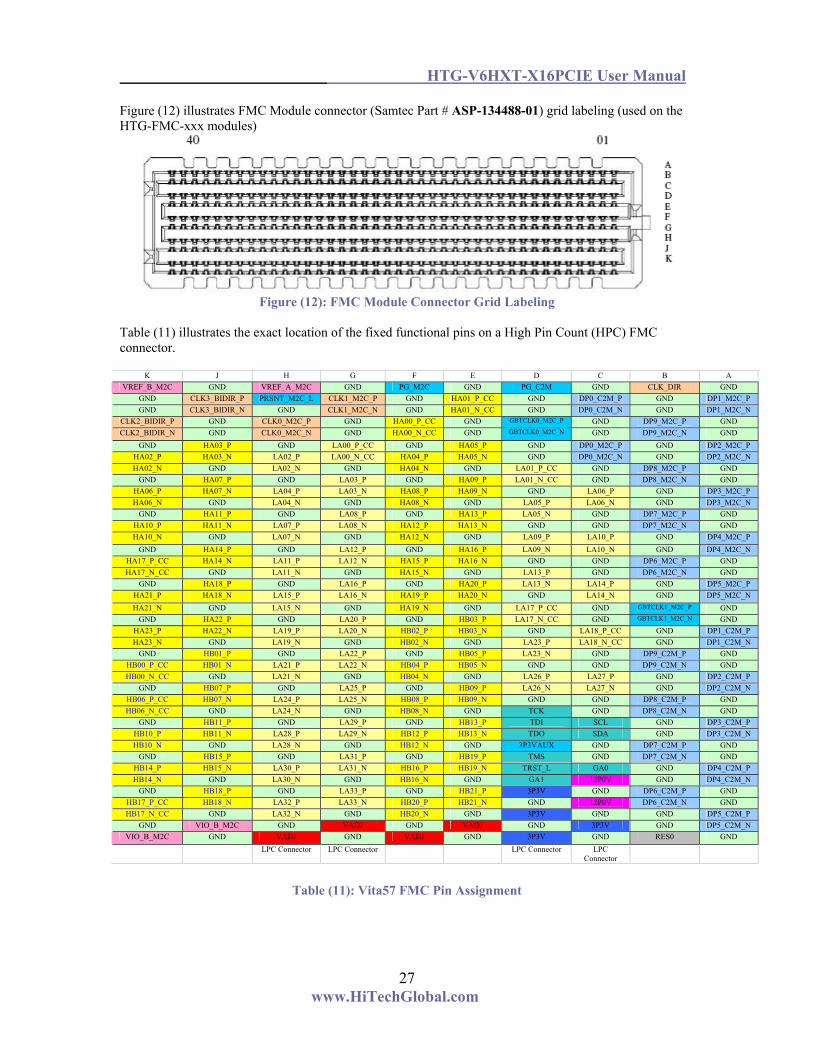
Figure (12) illustrates FMC Module connector (Samtec Part # ASP-134488-01) grid labeling (used on the HTG-FMC-xxx modules)
Figure (12): FMC Module Connector Grid Labeling
Table (11) illustrates the exact location of the fixed functional pins on a High Pin Count (HPC) FMC connector.
K J H G F E D C B A VREF_B_M2C GND VREF_A_M2C GND PG_M2C GND PG_C2M GND CLK_DIR GND
GND CLK3_BIDIR_P PRSNT_M2C_L CLK1_M2C_P GND HA01_P_CC GND DP0_C2M_P GND DP1_M2C_P GND CLK3_BIDIR_N GND CLK1_M2C_N GND HA01_N_CC GND DP0_C2M_N GND DP1_M2C_N
CLK2_BIDIR_P GND CLK0_M2C_P GND HA00_P_CC GND GBTCLK0_M2C_P GND DP9_M2C_P GND CLK2_BIDIR_N GND CLK0_M2C_N GND HA00_N_CC GND GBTCLK0_M2C_N GND DP9_M2C_N GND
GND HA03_P GND LA00_P_CC GND HA05_P GND DP0_M2C_P GND DP2_M2C_P HA02_P HA03_N LA02_P LA00_N_CC HA04_P HA05_N GND DP0_M2C_N GND DP2_M2C_N HA02_N GND LA02_N GND HA04_N GND LA01_P_CC GND DP8_M2C_P GND
GND HA07_P GND LA03_P GND HA09_P LA01_N_CC GND DP8_M2C_N GND HA06_P HA07_N LA04_P LA03_N HA08_P HA09_N GND LA06_P GND DP3_M2C_P HA06_N GND LA04_N GND HA08_N GND LA05_P LA06_N GND DP3_M2C_N
GND HA11_P GND LA08_P GND HA13_P LA05_N GND DP7_M2C_P GND HA10_P HA11_N LA07_P LA08_N HA12_P HA13_N GND GND DP7_M2C_N GND HA10_N GND LA07_N GND HA12_N GND LA09_P LA10_P GND DP4_M2C_P
GND HA14_P GND LA12_P GND HA16_P LA09_N LA10_N GND DP4_M2C_N HA17_P_CC HA14_N LA11_P LA12_N HA15_P HA16_N GND GND DP6_M2C_P GND HA17_N_CC GND LA11_N GND HA15_N GND LA13_P GND DP6_M2C_N GND
GND HA18_P GND LA16_P GND HA20_P LA13_N LA14_P GND DP5_M2C_P HA21_P HA18_N LA15_P LA16_N HA19_P HA20_N GND LA14_N GND DP5_M2C_N HA21_N GND LA15_N GND HA19_N GND LA17_P_CC GND GBTCLK1_M2C_P GND
GND HA22_P GND LA20_P GND HB03_P LA17_N_CC GND GBTCLK1_M2C_N GND HA23_P HA22_N LA19_P LA20_N HB02_P HB03_N GND LA18_P_CC GND DP1_C2M_P HA23_N GND LA19_N GND HB02_N GND LA23_P LA18_N_CC GND DP1_C2M_N
GND HB01_P GND LA22_P GND HB05_P LA23_N GND DP9_C2M_P GND HB00_P_CC HB01_N LA21_P LA22_N HB04_P HB05_N GND GND DP9_C2M_N GND HB00_N_CC GND LA21_N GND HB04_N GND LA26_P LA27_P GND DP2_C2M_P
GND HB07_P GND LA25_P GND HB09_P LA26_N LA27_N GND DP2_C2M_N HB06_P_CC HB07_N LA24_P LA25_N HB08_P HB09_N GND GND DP8_C2M_P GND HB06_N_CC GND LA24_N GND HB08_N GND TCK GND DP8_C2M_N GND
GND HB11_P GND LA29_P GND HB13_P TDI SCL GND DP3_C2M_P HB10_P HB11_N LA28_P LA29_N HB12_P HB13_N TDO SDA GND DP3_C2M_N HB10_N GND LA28_N GND HB12_N GND 3P3VAUX GND DP7_C2M_P GND
GND HB15_P GND LA31_P GND HB19_P TMS GND DP7_C2M_N GND HB14_P HB15_N LA30_P LA31_N HB16_P HB19_N TRST_L GA0 GND DP4_C2M_P HB14_N GND LA30_N GND HB16_N GND GA1 12P0V GND DP4_C2M_N
GND HB18_P GND LA33_P GND HB21_P 3P3V GND DP6_C2M_P GND HB17_P_CC HB18_N LA32_P LA33_N HB20_P HB21_N GND 12P0V DP6_C2M_N GND HB17_N_CC GND LA32_N GND HB20_N GND 3P3V GND GND DP5_C2M_P
GND VIO_B_M2C GND VADJ GND VADJ GND 3P3V GND DP5_C2M_N VIO_B_M2C GND VADJ GND VADJ GND 3P3V GND RES0 GND
LPC Connector LPC Connector LPC Connector LPC Connector
Table (11): Vita57 FMC Pin Assignment

HTG-V6HXT-X16PCIE User Manual
www.HiTechGlobal.com
28
2.9.1 FMC “A” Table (12) illustrates FPGA pin assignment for the FMC “A” (J7 –located on the left side of the board)
Column “B” Column “A”
FMC Pin Name Pin Description FPGA Pin #
FMC Pin Name Pin Description FPGA
Pin # 1 CLK_DIR FMC_A_CLK_SEL C14 1 GND GND
2 GND GND 2 DP1_M2C_P MGTRXP1_106 T39
3 GND GND 3 DP1_M2C_N MGTRXN1_106 T40
4 DP9_M2C_P MGTRXP0_108_ G37 4 GND GND
5 DP9_M2C_N MGTRXN0_108_ G38 5 GND GND
6 GND GND 6 DP2_M2C_P MGTRXP3_106_ M39
7 GND GND 7 DP2_M2C_N MGTRXN3_106_ M40
8 DP8_M2C_P MGTRXP1_108_ F39 8 GND GND
9 DP8_M2C_N MGTRXN1_108_ F40 9 GND GND
10 GND GND 10 DP3_M2C_P MGTRXP2_106_ N37
11 GND GND 11 DP3_M2C_N MGTRXN2_106_ N38
12 DP7_M2C_P MGTRXP0_107_ K39 12 GND GND
13 DP7_M2C_N MGTRXN0_107_ K40 13 GND GND
14 GND GND 14 DP4_M2C_P MGTRXP1_107_ L37
15 GND GND 15 DP4_M2C_N MGTRXN1_107_ L38
16 DP6_M2C_P MGTRXP3_107_ J37 16 GND GND
17 DP6_M2C_N MGTRXN3_107_ J38 17 GND GND
18 GND GND 18 DP5_M2C_P MGTRXP2_107_ H39
18 GND GND 18 DP5_M2C_N MGTRXN2_107_ H40
20 GBTCLK1_M2C_P MGTREFCLKP_107_ J41 20 GND GND
21 GBTCLK1_M2C_N MGTREFCLKN_107_ J42 21 GND GND
22 GND GND 22 DP1_C2M_P MGTTXP1_106_ P43
23 GND GND 23 DP1_C2M_N MGTTXN1_106_ P44
24 DP9_C2M_P MGTTXP0_108_ F43 24 GND GND
25 DP9_C2M_N MGTTXN0_108_ F44 25 GND GND
26 GND GND 26 DP2_C2M_P MGTTXP3_106_ N41
27 GND GND 27 DP2_C2M_N MGTTXN3_106_ N42
28 DP8_C2M_P MGTTXP1_108_ D43 28 GND GND
29 DP8_C2M_N MGTTXN1_108_ D44 29 GND GND
30 GND GND 30 DP3_C2M_P MGTTXP2_106_ M43
31 GND GND 31 DP3_C2M_N MGTTXN2_106_ M44
32 DP7_C2M_P MGTTXP0_107_ L41 32 GND GND
33 DP7_C2M_N MGTTXN0_107_ L42 33 GND GND
34 GND GND 34 DP4_C2M_P MGTTXP1_107_ K43
35 GND GND 35 DP4_C2M_N MGTTXN1_107_ K44
36 DP6_C2M_P MGTTXP3_107_ H43 36 GND GND
37 DP6_C2M_N MGTTXN3_107_ H44 37 GND GND
38 GND GND 38 DP5_C2M_P MGTTXP2_107_ G41
39 GND GND 39 DP5_C2M_N MGTTXN2_107_ G42
40 RES0 40 GND GND

HTG-V6HXT-X16PCIE User Manual
www.HiTechGlobal.com
29
Column “D” Column “ C”
FMC Pin Name Pin Description FPGA Pin #
FMC Pin Name Pin Description FPGA
Pin # 1 PG_C2M Power Good E10 1 GND NC
2 GND GND 2 DP0_C2M_P MGTTXP0_106_ T43
3 GND GND 3 DP0_C2M_N MGTTXN0_106_ T44
4 GBTCLK0_M2C_P MGTREFCLKP_106_ R41 4 GND GND
5 GBTCLK0_M2C_N MGTREFCLKN_106_ R42 5 GND GND
6 GND GND 6 DP0_M2C_P MGTRXP0_106_ U41
7 GND GND 7 DP0_M2C_N MGTRXN0_106_ U42
8 LA01_P_CC User defined signal E15 8 GND GND
9 LA01_N_CC User defined signal D15 9 GND GND
10 GND GND 10 LA06_P User defined signal K15
11 LA05_P User defined signal T15 11 LA06_N User defined signal J15
12 LA05_N User defined signal R15 12 GND GND
13 GND GND 13 GND GND
14 LA09_P User defined signal NC 14 LA10_P User defined signal NC
15 LA09_N User defined signal NC 15 LA10_N User defined signal NC
16 GND GND 16 GND GND
17 LA13_P User defined signal NC 17 GND GND
18 LA13_N User defined signal NC 18 LA14_P User defined signal NC
18 GND GND 18 LA14_N User defined signal NC
20 LA17_P_CC User defined signal NC 20 GND GND
21 LA17_N_CC User defined signal NC 21 GND GND
22 GND GND 22 LA18_P_CC User defined signal NC
23 LA23_P User defined signal NC 23 LA18_N_CC User defined signal NC
24 LA23_N User defined signal NC 24 GND GND
25 GND GND 25 GND GND
26 LA26_P User defined signal NC 26 LA27_P User defined signal NC
27 LA26_N User defined signal NC 27 LA27_N User defined signal NC
28 GND GND 28 GND GND
29 TCK JTAG 29 GND GND
30 TDI JTAG 30 SCL I2C serial clock. H11
31 TDO JTAG 31 SDA I2C serial data. B12
32 3P3VAUX 3.3V Aux. Supply 32 GND GND
33 TMS JTAG 33 GND GND
34 TRST_L Asynch. Init. 34 GA0 Geographical address
35 GA1 Geographical address 35 12P0V 12V Supply
36 3P3V 3.3V Supply 36 GND GND
37 GND GND 37 12P0V 12V Supply
38 3P3V 3.3V Supply 38 GND GND
39 GND GND 39 3P3V 3.3V Supply
40 3P3V 3.3V Supply 40 GND GND

HTG-V6HXT-X16PCIE User Manual
www.HiTechGlobal.com
30
Column “F” Column “E”
FMC Pin Name Pin Description FPGA Pin #
FMC Pin Name Pin Description FPGA
Pin # 1 PG_M2C Power Good F10 1 GND GND
2 GND GND GND 2 HA01_P_CC User defined signal NC
3 GND GND GND 3 HA01_N_CC User defined signal NC
4 HA00_P_CC User defined signal NC 4 GND GND GND
5 HA00_N_CC User defined signal NC 5 GND GND GND
6 GND GND GND 6 HA05_P User defined signal NC
7 HA04_P User defined signal NC 7 HA05_N User defined signal NC
8 HA04_N User defined signal NC 8 GND GND GND
9 GND GND GND 9 HA09_P User defined signal NC
10 HA08_P User defined signal NC 10 HA09_N User defined signal NC
11 HA08_N User defined signal NC 11 GND GND GND
12 GND GND GND 12 HA13_P User defined signal NC
13 HA12_P User defined signal NC 13 HA13_N User defined signal NC
14 HA12_N User defined signal NC 14 GND GND GND
15 GND GND GND 15 HA16_P User defined signal NC
16 HA15_P User defined signal NC 16 HA16_N User defined signal NC
17 HA15_N User defined signal NC 17 GND GND GND
18 GND GND GND 18 HA20_P User defined signal NC
18 HA19_P User defined signal NC 18 HA20_N User defined signal NC
20 HA19_N User defined signal NC 20 GND GND GND
21 GND GND GND 21 HB03_P User defined signal NC
22 HB02_P User defined signal NC 22 HB03_N User defined signal NC
23 HB02_N User defined signal NC 23 GND GND GND
24 GND GND GND 24 HB05_P User defined signal NC
25 HB04_P User defined signal NC 25 HB05_N User defined signal NC
26 HB04_N User defined signal NC 26 GND GND GND
27 GND GND GND 27 HB09_P User defined signal NC
28 HB08_P User defined signal NC 28 HB09_N User defined signal NC
29 HB08_N User defined signal NC 29 GND GND GND
30 GND GND GND 30 HB13_P User defined signal NC
31 HB12_P User defined signal NC 31 HB13_N User defined signal NC
32 HB12_N User defined signal NC 32 GND GND GND
33 GND GND GND 33 HB19_P User defined signal NC
34 HB16_P User defined signal NC 34 HB19_N User defined signal NC
35 HB16_N User defined signal NC 35 GND GND GND
36 GND GND GND 36 HB21_P User defined signal NC
37 HB20_P User defined signal NC 37 HB21_N User defined signal NC
38 HB20_N User defined signal NC 38 GND GND GND
39 GND GND GND 39 VADJ Adjustable Voltage
40 VADJ Adjustable Voltage 40 GND GND GND

HTG-V6HXT-X16PCIE User Manual
www.HiTechGlobal.com
31
Column “H” Column “G”
FMC Pin Name Pin Description FPGA Pin #
FMC Pin Name Pin Description FPGA
Pin # 1 VREF_A_M2C Reference voltage 1 GND GND
2 PRSNT_M2C_L Present Signal E30 2 CLK1_M2C_P Differential Clock NC
3 GND GND 3 CLK1_M2C_N Differential Clock NC
4 CLK0_M2C_P Differential Clock N11 4 GND GND
5 CLK0_M2C_N Differential Clock M10 5 GND GND
6 GND GND 6 LA00_P_CC User defined signal P13
7 LA02_P User defined signal E13 7 LA00_N_CC User defined signal N13
8 LA02_N User defined signal D13 8 GND GND
9 GND GND 9 LA03_P User defined signal H14
10 LA04_P User defined signal M15 10 LA03_N User defined signal G14
11 LA04_N User defined signal L15 11 GND GND
12 GND GND 12 LA08_P User defined signal K13
13 LA07_P User defined signal L14 13 LA08_N User defined signal J13
14 LA07_N User defined signal L13 14 GND GND
15 GND GND 15 LA12_P User defined signal NC
16 LA11_P User defined signal NC 16 LA12_N User defined signal NC
17 LA11_N User defined signal NC 17 GND GND
18 GND GND 18 LA16_P User defined signal NC
18 LA15_P User defined signal NC 18 LA16_N User defined signal NC
20 LA15_N User defined signal NC 20 GND GND
21 GND GND 21 LA20_P User defined signal NC
22 LA19_P User defined signal NC 22 LA20_N User defined signal NC
23 LA19_N User defined signal NC 23 GND GND
24 GND GND 24 LA22_P User defined signal NC
25 LA21_P User defined signal NC 25 LA22_N User defined signal NC
26 LA21_N User defined signal NC 26 GND GND
27 GND GND 27 LA25_P User defined signal NC
28 LA24_P User defined signal NC 28 LA25_N User defined signal NC
29 LA24_N User defined signal NC 29 GND GND
30 GND GND 30 LA29_P User defined signal NC
31 LA28_P User defined signal NC 31 LA29_N User defined signal NC
32 LA28_N User defined signal NC 32 GND GND
33 GND 33 LA31_P User defined signal NC
34 LA30_P User defined signal NC 34 LA31_N User defined signal NC
35 LA30_N User defined signal NC 35 GND GND
36 GND 36 LA33_P User defined signal NC
37 LA32_P User defined signal NC 37 LA33_N User defined signal NC
38 LA32_N User defined signal NC 38 GND GND
39 GND GND 39 VADJ Adjustable Voltage
40 VADJ Adjustable Voltage 40 GND GND

HTG-V6HXT-X16PCIE User Manual
www.HiTechGlobal.com
32
Column “K” Column “J”
FMC Pin Name Pin Description FPGA Pin #
FMC Pin Name Pin Description FPGA
Pin # 1 VREF_B_M2C Reference voltage 1 GND GND
2 GND GND 2 CLK3_M2C_P Differential Clock NC
3 GND GND 3 CLK3_M2C_N Differential Clock NC
4 CLK2_M2C_P FMC_A_CLK[2]_BI_P 4 GND GND
5 CLK2_M2C_N FMC_A_CLK[2]_BI_N 5 GND GND
6 GND GND 6 HA03_P User defined signal NC
7 HA02_P User defined signal NC 7 HA03_N User defined signal NC
8 HA02_N User defined signal NC 8 GND GND
9 GND GND 9 HA07_P User defined signal NC
10 HA06_P User defined signal NC 10 HA07_N User defined signal NC
11 HA06_N User defined signal NC 11 GND GND
12 GND GND 12 HA11_P User defined signal NC
13 HA10_P User defined signal NC 13 HA11_N User defined signal NC
14 HA10_N User defined signal NC 14 GND GND
15 GND GND 15 HA14_P User defined signal NC
16 HA17_P_CC User defined signal NC 16 HA14_N User defined signal NC
17 HA17_N_CC User defined signal NC 17 GND GND
18 GND GND 18 HA18_P User defined signal NC
18 HA21_P User defined signal NC 18 HA18_N User defined signal NC
20 HA21_N User defined signal NC 20 GND GND
21 GND GND 21 HA22_P User defined signal NC
22 HA23_P User defined signal NC 22 HA22_N User defined signal NC
23 HA23_N User defined signal NC 23 GND GND
24 GND GND 24 HB01_P User defined signal NC
25 HB00_P_CC User defined signal NC 25 HB01_N User defined signal NC
26 HB00_N_CC User defined signal NC 26 GND GND
27 GND GND 27 HB07_P User defined signal NC
28 HB06_P_CC User defined signal NC 28 HB07_N User defined signal NC
29 HB06_N_CC User defined signal NC 29 GND GND
30 GND GND 30 HB11_P User defined signal NC
31 HB10_P User defined signal NC 31 HB11_N User defined signal NC
32 HB10_N User defined signal NC 32 GND GND
33 GND GND 33 HB15_P User defined signal NC
34 HB14_P User defined signal NC 34 HB15_N User defined signal NC
35 HB14_N User defined signal NC 35 GND GND
36 GND GND 36 HB18_P User defined signal NC
37 HB17_P_CC User defined signal NC 37 HB18_N User defined signal NC
38 HB17_N_CC User defined signal NC 38 GND GND
39 GND GND 39 VIO_B_M2C IO Bank Voltage
40 VIO_B_M2C IO Bank Voltage 40 GND GND
Table (12): FPGA Mezzanine Connector (FMC “A”) pin assignment

HTG-V6HXT-X16PCIE User Manual
www.HiTechGlobal.com
33
2.9.1.1 FMC “A” Clock Generation Clock (selectable LVDS or LVPECL) for the GTH transceivers (GTH106, 107, and 108) on the FMC “A” is either provided through an add-on FMC module or the on-board SMA connectors X6 and X7 (external clock). The clock selection is controlled by the “S1” switch as follows: S1= 00 Clock supplied by the FMC_A_GBTCLK[0] S1= 01 Clock supplied by the FMC_A_GBTCLK[1] S1= 10 Clock supplied an external clock generator 2.9.1.2) V_adjust As illustrated by figure(13), V_adjust for the FMC “A” is set to 2.5V by default (R393=0 Ohm). By un-populating the R293 and populating either the R394 or R395with a “0” Ohm resistor changes the V_adjust voltage to 1.8V or 1.5V subsequently.
Figure (13): V_Adjust Configuration for FMC “A”

HTG-V6HXT-X16PCIE User Manual
www.HiTechGlobal.com
34
2.9.2) FMC “B” Table (13) illustrates FPGA pin assignment for the FMC “B” (J9 –located on the right side of the board)
Column “B” Column “A”
FMC Pin Name Pin Description FPGA Pin #
FMC Pin Name Pin Description FPGA
Pin # 1 CLK_DIR CLK_DIR P15 1 GND GND -
2 GND GND 2 DP1_M2C_P MGTRXP1_100_ BC42
3 GND GND 3 DP1_M2C_N MGTRXN1_100_ BC41
4 DP9_M2C_P MGTRXP1_102_ AM40 4 GND GND
5 DP9_M2C_N MGTRXN1_102_ AM39 5 GND GND
6 GND GND 6 DP2_M2C_P MGTRXP2_100_ BB40
7 GND GND 7 DP2_M2C_N MGTRXN2_100_ BB39
8 DP8_M2C_P MGTRXP0_102_ AL38 8 GND GND
9 DP8_M2C_N MGTRXN0_102_ AL37 9 GND GND
10 GND GND 10 DP3_M2C_P MGTRXP3_100_ BA42
11 GND GND 11 DP3_M2C_N MGTRXN3_100_ BA41
12 DP7_M2C_P MGTRXP0_101_ AY40 12 GND GND
13 DP7_M2C_N MGTRXN0_101_ AY39 13 GND GND
14 GND GND 14 DP4_M2C_P MGTRXP1_101_ AV40
15 GND GND 15 DP4_M2C_N MGTRXN1_101_ AV39
16 DP6_M2C_P MGTRXP2_101_ AT40 16 GND GND
17 DP6_M2C_N MGTRXN2_101_ AT39 17 GND GND
18 GND GND 18 DP5_M2C_P MGTRXP3_101_ AP40
18 GND GND 18 DP5_M2C_N MGTRXN3_101_ AP39
20 GBTCLK1_M2C_P MGTREFCLK0P_101_ AU37 20 GND GND
21 GBTCLK1_M2C_N MGTREFCLK0N_101_ AU38 21 GND GND
22 GND GND 22 DP1_C2M_P MGTTXP1_100_ AY44
23 GND GND 23 DP1_C2M_N MGTTXN1_100_ AY43
24 DP9_C2M_P MGTTXP1_102_ AM44 24 GND GND
25 DP9_C2M_N MGTTXN1_102_ AM43 25 GND GND
26 GND GND 26 DP2_C2M_P MGTTXP2_100_ AW42
27 GND GND 27 DP2_C2M_N MGTTXN2_100_ AW41
28 DP8_C2M_P MGTTXP0_102_ AN42 28 GND GND
29 DP8_C2M_N MGTTXN0_102_ AN41 29 GND GND
30 GND GND 30 DP3_C2M_P MGTTXP3_100_ AV44
31 GND GND 31 DP3_C2M_N MGTTXN3_100_ AV43
32 DP7_C2M_P MGTTXP0_101_ AU42 32 GND GND
33 DP7_C2M_N MGTTXN0_101_ AU41 33 GND GND
34 GND GND 34 DP4_C2M_P MGTTXP1_101_ AT44
35 GND GND 35 DP4_C2M_N MGTTXN1_101_ AT43
36 DP6_C2M_P MGTTXP2_101_ AR42 36 GND GND
37 DP6_C2M_N MGTTXN2_101_ AR41 37 GND GND
38 GND GND 38 DP5_C2M_P MGTTXP3_101_ AP44
39 GND GND 39 DP5_C2M_N MGTTXN3_101_ AP43
40 RES0 NC 40 GND GND

HTG-V6HXT-X16PCIE User Manual
www.HiTechGlobal.com
35
Column “D” Column “ C”
FMC Pin Name Pin Description FPGA
Pin # FMC Pin
Name Pin Description FPGA Pin #
1 PG_C2M Power Good 1 GND GND
2 GND GND 2 DP0_C2M_P MGTTXP0_100_ BB34
3 GND GND 3 DP0_C2M_N MGTTXN0_100_ BB43
4 GBTCLK0_M2C_P MGTREFCLK0P_100_ BA37 4 GND GND
5 GBTCLK0_M2C_N MGTREFCLK0N_100_ BA38 5 GND GND
6 GND GND 6 DP0_M2C_P MGTRXP0_100_ BD40
7 GND GND 7 DP0_M2C_N MGTRXN0_100_ BD39
8 LA01_P_CC User defined signal M35 8 GND GND
9 LA01_N_CC User defined signal L35 9 GND GND
10 GND GND 10 LA06_P User defined signal B37
11 LA05_P User defined signal E35 11 LA06_N User defined signal A37
12 LA05_N User defined signal D35 12 GND GND
13 GND GND 13 GND GND
14 LA09_P User defined signal D33 14 LA10_P User defined signal B35
15 LA09_N User defined signal D34 15 LA10_N User defined signal B36
16 GND GND 16 GND GND
17 LA13_P User defined signal A34 17 GND GND
18 LA13_N User defined signal A35 18 LA14_P User defined signal C34
18 GND GND 18 LA14_N User defined signal B34
20 LA17_P_CC User defined signal J31 20 GND GND
21 LA17_N_CC User defined signal H32 21 GND GND
22 GND GND 22 LA18_P_CC User defined signal R28
23 LA23_P User defined signal R30 23 LA18_N_CC User defined signal P29
24 LA23_N User defined signal P30 24 GND GND
25 GND GND 25 GND GND
26 LA26_P User defined signal T29 26 LA27_P User defined signal C32
27 LA26_N User defined signal T30 27 LA27_N User defined signal C33
28 GND GND 28 GND GND
29 TCK JTAG 29 GND GND
30 TDI JTAG 30 SCL I2C serial clock.
31 TDO JTAG 31 SDA I2C serial data.
32 3P3VAUX 3.3V Aux. Supply 32 GND GND -
33 TMS JTAG 33 GND GND -
34 TRST_L Asynch. Init. 34 GA0 Geographical address
35 GA1 Geographical
address 35 12P0V 12V Supply
36 3P3V 3.3V Supply 36 GND GND
37 GND GND 37 12P0V 12V Supply
38 3P3V 3.3V Supply 38 GND GND
39 GND GND 39 3P3V 3.3V Supply
40 3P3V 3.3V Supply 40 GND GND

HTG-V6HXT-X16PCIE User Manual
www.HiTechGlobal.com
36
Column “F” Column “E”
FMC Pin Name Pin Description FPGA
Pin # FMC Pin
Name Pin Description FPGA Pin #
1 PG_M2C Power Good M31 1 GND
2 GND 2 HA01_P_CC User defined signal NC
3 GND 3 HA01_N_CC User defined signal NC
4 HA00_P_CC User defined signal NC 4 GND
5 HA00_N_CC User defined signal NC 5 GND
6 GND 6 HA05_P User defined signal NC
7 HA04_P User defined signal NC 7 HA05_N User defined signal NC
8 HA04_N User defined signal NC 8 GND
9 GND 9 HA09_P User defined signal NC
10 HA08_P User defined signal NC 10 HA09_N User defined signal NC
11 HA08_N User defined signal NC 11 GND
12 GND 12 HA13_P User defined signal NC
13 HA12_P User defined signal NC 13 HA13_N User defined signal NC
14 HA12_N User defined signal NC 14 GND
15 GND 15 HA16_P User defined signal NC
16 HA15_P User defined signal NC 16 HA16_N User defined signal NC
17 HA15_N User defined signal NC 17 GND
18 GND 18 HA20_P User defined signal NC
18 HA19_P User defined signal NC 18 HA20_N User defined signal NC
20 HA19_N User defined signal NC 20 GND
21 GND 21 HB03_P User defined signal NC
22 HB02_P User defined signal NC 22 HB03_N User defined signal NC
23 HB02_N User defined signal NC 23 GND
24 GND 24 HB05_P User defined signal NC
25 HB04_P User defined signal NC 25 HB05_N User defined signal NC
26 HB04_N User defined signal NC 26 GND
27 GND 27 HB09_P User defined signal NC
28 HB08_P User defined signal NC 28 HB09_N User defined signal NC
29 HB08_N User defined signal NC 29 GND
30 GND 30 HB13_P User defined signal NC
31 HB12_P User defined signal NC 31 HB13_N User defined signal NC
32 HB12_N User defined signal NC 32 GND
33 GND 33 HB19_P User defined signal NC
34 HB16_P User defined signal NC 34 HB19_N User defined signal NC
35 HB16_N User defined signal NC 35 GND
36 GND 36 HB21_P User defined signal NC
37 HB20_P User defined signal NC 37 HB21_N User defined signal NC
38 HB20_N User defined signal NC 38 GND
39 GND 39 VADJ Adjustable Voltage
40 VADJ Adjustable Voltage 40 GND

HTG-V6HXT-X16PCIE User Manual
www.HiTechGlobal.com
37
Column “H” Column “G”
FMC Pin Name Pin Description FPGA Pin #
FMC Pin Name Pin Description FPGA
Pin # 1 VREF_A_M2C Reference voltage D30 1 GND GND
2 PRSNT_M2C_L Present Signal L30 2 CLK1_M2C_P Differential Clock NC
3 GND GND 3 CLK1_M2C_N Differential Clock NC
4 CLK0_M2C_P Differential Clock AN33 4 GND GND
5 CLK0_M2C_N Differential Clock AP34 5 GND GND
6 GND GND 6 LA00_P_CC User defined signal N33
7 LA02_P User defined signal G35 7 LA00_N_CC User defined signal N34
8 LA02_N User defined signal F35 8 GND GND
9 GND GND 9 LA03_P User defined signal K35
10 LA04_P User defined signal J33 10 LA03_N User defined signal J35
11 LA04_N User defined signal H33 11 GND GND
12 GND GND 12 LA08_P User defined signal F33
13 LA07_P User defined signal J34 13 LA08_N User defined signal E33
14 LA07_N User defined signal H34 14 GND GND
15 GND GND 15 LA12_P User defined signal L33
16 LA11_P User defined signal R33 16 LA12_N User defined signal K33
17 LA11_N User defined signal P33 17 GND GND
18 GND GND 18 LA16_P User defined signal P31
18 LA15_P User defined signal R31 18 LA16_N User defined signal N32
20 LA15_N User defined signal R32 20 GND GND
21 GND GND 21 LA20_P User defined signal G31
22 LA19_P User defined signal H31 22 LA20_N User defined signal F32
23 LA19_N User defined signal G32 23 GND GND
24 GND GND 24 LA22_P User defined signal B30
25 LA21_P User defined signal G30 25 LA22_N User defined signal A30
26 LA21_N User defined signal F30 26 GND GND
27 GND GND 27 LA25_P User defined signal K30
28 LA24_P User defined signal L32 28 LA25_N User defined signal J30
29 LA24_N User defined signal K32 29 GND GND
30 GND GND 30 LA29_P User defined signal B32
31 LA28_P User defined signal M30 31 LA29_N User defined signal A33
32 LA28_N User defined signal M31 32 GND GND
33 GND GND 33 LA31_P User defined signal E31
34 LA30_P User defined signal N29 34 LA31_N User defined signal E32
35 LA30_N User defined signal M29 35 GND GND
36 GND GND 36 LA33_P User defined signal B31
37 LA32_P User defined signal D31 37 LA33_N User defined signal A32
38 LA32_N User defined signal C31 38 GND GND
39 GND GND 39 VADJ Adjustable Voltage
40 VADJ Adjustable Voltage 40 GND GND

HTG-V6HXT-X16PCIE User Manual
www.HiTechGlobal.com
38
Column “K” Column “J”
FMC Pin Name Pin Description FPGA Pin #
FMC Pin Name Pin Description FPGA
Pin # 1 VREF_B_M2C Reference voltage 1 GND
2 GND 2 CLK3_M2C_P Differential Clock NC
3 GND 3 CLK3_M2C_N Differential Clock NC
4 CLK2_M2C_P Differential Clock NC 4 GND
5 CLK2_M2C_N Differential Clock NC 5 GND
6 GND 6 HA03_P User defined signal NC
7 HA02_P User defined signal NC 7 HA03_N User defined signal NC
8 HA02_N User defined signal NC 8 GND
9 GND 9 HA07_P User defined signal NC
10 HA06_P User defined signal NC 10 HA07_N User defined signal NC
11 HA06_N User defined signal NC 11 GND
12 GND 12 HA11_P User defined signal NC
13 HA10_P User defined signal NC 13 HA11_N User defined signal NC
14 HA10_N User defined signal NC 14 GND
15 GND 15 HA14_P User defined signal NC
16 HA17_P_CC User defined signal NC 16 HA14_N User defined signal NC
17 HA17_N_CC User defined signal NC 17 GND
18 GND 18 HA18_P User defined signal NC
18 HA21_P User defined signal NC 18 HA18_N User defined signal NC
20 HA21_N User defined signal NC 20 GND
21 GND 21 HA22_P User defined signal NC
22 HA23_P User defined signal NC 22 HA22_N User defined signal NC
23 HA23_N User defined signal NC 23 GND
24 GND 24 HB01_P User defined signal NC
25 HB00_P_CC User defined signal NC 25 HB01_N User defined signal NC
26 HB00_N_CC User defined signal NC 26 GND
27 GND 27 HB07_P User defined signal NC
28 HB06_P_CC User defined signal NC 28 HB07_N User defined signal NC
29 HB06_N_CC User defined signal NC 29 GND
30 GND 30 HB11_P User defined signal NC
31 HB10_P User defined signal NC 31 HB11_N User defined signal NC
32 HB10_N User defined signal NC 32 GND
33 GND 33 HB15_P User defined signal NC
34 HB14_P User defined signal NC 34 HB15_N User defined signal NC
35 HB14_N User defined signal NC 35 GND
36 GND 36 HB18_P User defined signal NC
37 HB17_P_CC User defined signal NC 37 HB18_N User defined signal NC
38 HB17_N_CC User defined signal NC 38 GND
39 GND 39 VIO_B_M2C IO Bank Voltage
40 VIO_B_M2C IO Bank Voltage 40 GND
Table (13): FPGA Mezzanine Connector (FMC “B”) pin assignment

HTG-V6HXT-X16PCIE User Manual
www.HiTechGlobal.com
39
◙ 2.10) USB To UART Bridge
The HTG-V6HXT-X16PCIE board provides one UART port through a peripheral USB connector. The port is supported by the Silicon labs CP2102 USB to UART controller chip. The CP2102 is a highly-integrated USB-to-UART Bridge Controller providing a simple solution for updating RS-232 designs to USB using a minimum of components and PCB space. The CP2102 includes a USB 2.0 full-speed function controller, USB transceiver, oscillator, EEPROM, and asynchronous serial data bus (UART) with full modem control signals in a compact 5 x 5 mm QFN-28 package. No other external USB components are required. The on-chip EEPROM may be used to customize the USB Vendor ID, Product ID, Product Description String, Power Descriptor, Device Release Number, and Device Serial Number as desired for OEM applications. The EEPROM is programmed on-board via the USB, allowing the programming step to be easily integrated into the product manufacturing and testing process. Virtual COM Port (VCP) device drivers provided by Silicon Laboratories allow a CP2102-based product to appear as a COM port to PC applications. The CP2102 UART interface implements all RS-232 signals, including control and handshaking signals, so existing system firmware does not need to be modified. In many existing RS-232 designs, all that is required to update the design from RS-232 to USB is to replace the RS-232 level-translator with the CP2102. Direct access driver support is available through the Silicon Laboratories USBXpress driver set. There are two sets of device drivers available for the CP2102 devices: the Virtual COM Port (VCP) drivers and the USBXpress Direct Access drivers. Only one set of drivers is necessary to interface with the device. The latest drivers are available at: http://www.silabs.com/products/mcu/pages/usbtouartbridgevcpdrivers.aspx Additional device information is available at http://www.silabs.com/Support%20Documents/TechnicalDocs/cp2102.pdf Table (14) illustrates FPGA pin assignment for the USB-TO-UART interface:
UART/USB Bridge (U4) Signal Name FPGA (2U8) Pin # USB_PERI_PWR C12
UART_RST C11 UART_SUSPEND A13
UART_RI A12 UART_DCD B11 UART_DTR A10 UART_DSR R13 UART_RXD R12 UART_TXD A9 UART_RTS B9 UART_CTS C13
Table (14): USB To UART FPGA pin assignment

HTG-V6HXT-X16PCIE User Manual
www.HiTechGlobal.com
40
◙ 2.11) LEDs, GPIO Headers & Pushbuttons The HTG-V6HXT-X16PCIE provides user LEDs, Jumpers, and Push Buttons.
Signal Name Reference Designator FPGA/CPLD Pin # FPGA_USER_LED0 D26 AV33 FPGA_USER_LED1 D25 AW34 FPGA_USER_LED2 D24 AK35 FPGA_USER_LED3 D23 AL35 FPGA_USER_LED4 D29 E16 FPGA_USER_LED5 D30 D16 FPGA_USER_LED6 D28 J14 FPGA_USER_LED7 D27 H13 CPLD_USER_LED0 D34 G5 CPLD_USER_LED1 D35 H5 FPGA_USER_IO0 J13 (PIN 1) AW33 FPGA_USER_IO1 J13 (PIN 3) AY33 FPGA_USER_IO2 J13 (PIN 5) AW35 FPGA_USER_IO3 J13 (PIN 7) AY35 FPGA_USER_IO4 J13 (PIN 9) B14 FPGA_USER_IO5 J13 (PIN 11) A14 FPGA_USER_IO6 J13 (PIN 13) F14 FPGA_USER_IO7 J13 (PIN 15) F13 FPGA_USER_SW0 S2 (1) A17 FPGA_USER_SW1 S2 (2) B15 CPLD_USER_SW0 S2 (3) G4 CPLD_USER_SW1 S2 (4) G3 FPGA_USER_PB S3 B17
Table (15): User Interface FPGA pin assignment
◙ 2.12) Configuration Xilinx FPGAs are CMOS configurable latch (CCL) based and must be configured at power-up from a non-volatile source. FPGA configuration is traditionally accomplished with a JTAG interface, a microprocessor, or the Xilinx PROMs (Platform Flash PROMs). The following configuration options are available for the HTG-V6HXT-X16PCIE platform:
1) Direct FPGA configuration through the onboard JTAG header (J12) 2) CPLD and two Xilinx PlatformXL flash devices (meets PCI Express link training time) 3) Micron G18 Embedded high-speed flash (meets PCI Express link training time)
Upon successful configuration D13 (DONE) LED illuminates and stays ON. Additional information is available at : http://www.xilinx.com/support/documentation/application_notes/xapp973.pdf

HTG-V6HXT-X16PCIE User Manual
www.HiTechGlobal.com
41
2.12.1) Jumper Setting: Table (16) illustrates jumper setting for devices in the JTAG chain .
Device in chain JP3 JP4 JP5 JP6
FPGA Only Shunt on Pin 1 &2
Shunt on Pin 2 &3
Shunt on Pin 2 &3
Shunt on Pin 2 &3
FPGA + CPLD Shunt on Pin 1 &2
Shunt on Pin 1 &2
Shunt on Pin 2 &3
Shunt on Pin 2 &3
FPGA + CPLD +FMC “A” Shunt on Pin 1 &2
Shunt on Pin 1 &2
Shunt on Pin 1 &2
Shunt on Pin 2 &3
FPGA + CPLD +FMC “A” + +FMC “B”
Shunt on Pin 1 &2
Shunt on Pin 1 &2
Shunt on Pin 1 &2
Shunt on Pin 1 &2
Table (16): JTAG Chain Configuration

HTG-V6HXT-X16PCIE User Manual
www.HiTechGlobal.com
42
Chapter 3:Mezannine Cards Vita 57 provides a mechanical standard for I/O mezzanine modules. This standard introduces a methodology that shall allow the front panel IO of IEEE 1101 form factor cards to be configured via mezzanine boards. Vita 57 modules have fixed locations for serial/parallel IOs, clocks, Jtag signals, VCC, and GND. HiTech Global's Vita 57 modules work with any Vita 57 compliant carrier boards. The FMC standard specifies Samtec’s SEARAY™ connector set. The VITA 57 SEAM/SEAF Series system provides 400 I/Os in a 40 x 10 configuration or 160 I/Os in a selectively loaded 40 x 10 configuration, in 8.5mm and 10mm stack heights. HiTech Global offers a wide range of FMC daughter cards which can be used for expanding functionality of the main board.
◙ 3.1) Dual SFP+
The Dual SFP+ FMC daughter card provides access to two SFP+ ports (10Gbps each) interfacing to total of 8 serial transceivers (XUAI).
The onboard 10Gig PHY device is a physical layer transceiver with an integrated Electronic Dispersion Compensation (EDC) engine - compliant with IEEE802.3aq specifications. The device integrates industry-leading SerDes/PHY technology with low-power EDC engine with up to 5db of margin over the symmetric stress test pulse sensitivity specifications defined in the 10GASE-LRM standard.
Each PHY device provides full PCS, PMA, and XGXS sub-layer functionality through the consolidation of the receiver and transmitter PHY functions on a single chip along with the integration of encode/decode/alignment logic, FIFOs, on-chip clock drivers, multiple loop-back features and PRBS & Ethernet frame generation & verification for both the line side and the system side.
More information is available at http://www.hitechglobal.com/FMCModules/FMC_SFP+.htm
◙ 3.2) Dual CX4
The dual CX4 FMC daughter card provides access to two CX4 ports (10Gbps) interfacing to total of 8 serial transceivers (XUAI). More information is available at http://www.hitechglobal.com/FMCModules/FMC_Dual_CX4.htm
◙ 3.3) CX4/SATA/SMA Serial Connectivity
The Serial Connectivity FMC daughter card provides access to one CX4, two SATA, and two SMA ports (interfacing to total of 8 serial transceivers). Each port has its own on-board dedicated clock for maximum flexibility and ease of use. More information is available at http://www.hitechglobal.com/FMCModules/FMC_CX4-SMA-SATA.htm
◙ 3.4) PCI Express Root Complex
The PCI Express Root FMC daughter card provides access to 8 lanes of PCI Express Gen 1 and port. The module is supported by 100MHz and 250MHz low-jitter clocks.

HTG-V6HXT-X16PCIE User Manual
www.HiTechGlobal.com
43
More information is available at http://www.hitechglobal.com/FMCModules/FMC_PCIExpress.htm
◙ 3..5) 8-Port SMA
The 8-Port SMA FMC daughter card provides access to 32 SMA connecters providing access to 8 Serial Transceivers. The module is supported by on-board and external clocks.
More information is available at http://www.hitechglobal.com/FMCModules/FMC_SMA.htm
◙ 3..6) Quad SFP/SATA The Quad SFP/SATA FMC daughter card provides access to four SFP and four SATA connectors. Each interface is supported by its own independent clock. More information is available at http://www.hitechglobal.com/FMCModules/FMC_x4SFP_x4SATA.htm
◙ 3.7) 16-bit Dual Channel DA/AD Conversion
The AD-DA FMC module plugs in to FMC HPC slot in a typical FMC based FPGA development board and provides dual 16 bit ADC and dual 16 bit DAC interfaces. This module has an interface where a RF card can be plugged in to provide up converter and down converter functionalities for any wireless band of interest. This module can be used for developing wireless PHY and MAC IP for the emerging wireless standards like LTE and WIMAX. The Gigabit serial IO can be used to connect to another similar system to provide MIMO functionality required for any new standards. More information is available at http://www.hitechglobal.com/FMCModules/16-bit_AD-DA.htm
Technical Support:
Technical support can be provided by contacting [email protected] Support requests are responded in less than 24 hours. Sales Support: Sales support can be provided by contacting [email protected] or +1 408 781-7778 (8:00 AM – 6:00 PM Pacific Standard Time)